WO2017064848A1 - Electric power conversion device and power conditioner using same - Google Patents
Electric power conversion device and power conditioner using sameDownload PDFInfo
- Publication number
- WO2017064848A1 WO2017064848A1PCT/JP2016/004484JP2016004484WWO2017064848A1WO 2017064848 A1WO2017064848 A1WO 2017064848A1JP 2016004484 WJP2016004484 WJP 2016004484WWO 2017064848 A1WO2017064848 A1WO 2017064848A1
- Authority
- WO
- WIPO (PCT)
- Prior art keywords
- switching element
- point
- output
- connection point
- capacitor
- Prior art date
- Legal status (The legal status is an assumption and is not a legal conclusion. Google has not performed a legal analysis and makes no representation as to the accuracy of the status listed.)
- Ceased
Links
Images


Classifications
- H—ELECTRICITY
- H02—GENERATION; CONVERSION OR DISTRIBUTION OF ELECTRIC POWER
- H02M—APPARATUS FOR CONVERSION BETWEEN AC AND AC, BETWEEN AC AND DC, OR BETWEEN DC AND DC, AND FOR USE WITH MAINS OR SIMILAR POWER SUPPLY SYSTEMS; CONVERSION OF DC OR AC INPUT POWER INTO SURGE OUTPUT POWER; CONTROL OR REGULATION THEREOF
- H02M7/00—Conversion of AC power input into DC power output; Conversion of DC power input into AC power output
- H02M7/42—Conversion of DC power input into AC power output without possibility of reversal
- H02M7/44—Conversion of DC power input into AC power output without possibility of reversal by static converters
- H02M7/48—Conversion of DC power input into AC power output without possibility of reversal by static converters using discharge tubes with control electrode or semiconductor devices with control electrode
- H02M7/483—Converters with outputs that each can have more than two voltages levels
Definitions
- the present inventionrelates to a power conversion device and a power conditioner using the same.
- Patent Documents 1 and 2disclose a power converter that generates an AC output converted from a DC voltage source into a plurality of voltage levels (“Multi-level power converter” in Patent Document 1 and “Converter Circuit” in Patent Document 2). Is disclosed.
- the power conversion deviceis a 5-level inverter that outputs a 5-level voltage, and includes two DC capacitors, two flying capacitors, and 10 switching elements. ing.
- the voltage of each DC capacitorbecomes E / 2 and the voltage of each flying capacitor becomes E / 4.
- the switching elementBy controlling the switching element, a five-level voltage is output.
- Japanese Patent Laying-Open No. 2014-64431paragraphs [0002] to [0006], FIGS. 16 and 17
- Japanese Patent No. 4369425Japanese Patent No. 4369425
- the present inventionhas been made in view of the above reasons, and an object thereof is to provide a power conversion device capable of further improving the power conversion efficiency and a power conditioner using the power conversion device.
- a power conversion deviceincludes a first conversion circuit and a second conversion circuit, and includes a first bidirectional switch, a second bidirectional switch, and first to fourth protection diodes. It has more.
- the first conversion circuit and the second conversion circuitare electrically in parallel between a first input point on the high potential side of the DC power supply and a second input point on the low potential side of the DC power supply. It is connected.
- the first conversion circuitincludes first to fourth switching elements and a first capacitor.
- the first to fourth switching elementsinclude a first switching element, a second switching element, and a third switching element from the first input point side between the first input point and the second input point. In this order, the fourth switching elements are electrically connected in series.
- the first capacitoris electrically connected in parallel with a series circuit of the second switching element and the third switching element.
- the first conversion circuituses a connection point between the second switching element and the third switching element as a first output point.
- the second conversion circuitincludes fifth to eighth switching elements and a second capacitor.
- the fifth to eighth switching elementsinclude a fifth switching element, a sixth switching element, and a seventh switching element from the first input point side between the first input point and the second input point. In this order, the eighth switching elements are electrically connected in series.
- the second capacitoris electrically connected in parallel with a series circuit of the sixth switching element and the seventh switching element.
- the second conversion circuituses a connection point between the sixth switching element and the seventh switching element as a second output point.
- the first bidirectional switchis a connection point between a first connection point, which is a connection point between the first switching element and the second switching element, and a connection point between the seventh switching element and the eighth switching element.
- the second connection pointis electrically connected.
- the second bidirectional switchis a connection point of a third connection point that is a connection point of the third switching element and the fourth switching element, and a connection point of the fifth switching element and the sixth switching element. It is electrically connected to the fourth connection point.
- the first protection diodeis electrically connected in parallel with a series circuit of the first switching element and the second switching element between the first input point and the first output point, A current flowing from the first output point to the first input point is passed.
- the second protection diodeis electrically connected in parallel with a series circuit of the third switching element and the fourth switching element between the second input point and the first output point, A current flowing from the second input point to the first output point is passed.
- the third protection diodeis electrically connected in parallel with a series circuit of the fifth switching element and the sixth switching element between the first input point and the second output point, A current flowing from the second output point to the first input point is passed.
- the fourth protection diodeis electrically connected in parallel with a series circuit of the seventh switching element and the eighth switching element between the second input point and the second output point. A current flowing from the second input point to the second output point is passed.
- the power converteris configured to generate an output voltage between the first output point and the second output point.
- a power conditionerincludes the power conversion device described above and a disconnector electrically connected between the first output point and the second output point and a system power supply.
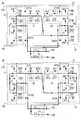
- FIG. 1is a circuit diagram illustrating a configuration of a power conversion device according to an embodiment.
- FIG. 2Ais an explanatory diagram of a first mode of the power conversion device according to the embodiment
- FIG. 2Bis an explanatory diagram of a second mode of the power conversion device according to the embodiment.
- FIG. 3Ais an explanatory diagram of a third mode of the power conversion device according to the embodiment
- FIG. 3Bis an explanatory diagram of a fourth mode of the power conversion device according to the embodiment.
- 4Ais an explanatory diagram of a fifth mode of the power conversion device according to the embodiment
- FIG. 4Bis an explanatory diagram of a sixth mode of the power conversion device according to the embodiment.
- FIG. 2Ais an explanatory diagram of a first mode of the power conversion device according to the embodiment
- FIG. 2Bis an explanatory diagram of a second mode of the power conversion device according to the embodiment.
- FIG. 3Ais an explanatory diagram of a third mode of the power
- FIG. 5Ais an explanatory diagram of a seventh mode of the power conversion device according to the embodiment
- FIG. 5Bis an explanatory diagram of an eighth mode of the power conversion device according to the embodiment
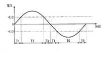
- FIG. 6is a waveform diagram of an output voltage of the power conversion device according to the embodiment.
- FIG. 7is a schematic diagram illustrating a configuration of a power conditioner according to the embodiment.
- FIG. 8is a waveform diagram showing the relationship between the output voltage and the output current of the power converter according to the embodiment.
- 9Ais an explanatory diagram of a dead time between the first and second modes of the power conversion device according to the embodiment
- FIG. 9Bis an explanatory diagram of a dead time between the first and third modes of the power conversion device according to the embodiment. is there.
- FIG. 10Ais an explanatory diagram of a dead time between the second and fourth modes of the power conversion device according to the embodiment
- FIG. 10Bis an explanatory diagram of a dead time between the third and fourth modes of the power conversion device according to the embodiment. is there.
- FIG. 11Ais an explanatory diagram of a dead time between the first and third modes of the power converter of the comparative example
- FIG. 11Bis an explanatory diagram of a third mode of the power converter of the comparative example.
- 12Ais an explanatory diagram of a dead time between the first and second modes of the power conversion device according to the embodiment
- FIG. 12Bis an explanatory diagram of a dead time between the first and third modes of the power conversion device according to the embodiment. is there.
- FIG. 11Ais an explanatory diagram of a dead time between the first and third modes of the power converter of the comparative example
- FIG. 12Bis an explanatory diagram of a dead time between the first and third modes of the power conversion device according to the
- FIG. 13Ais an explanatory diagram of a dead time between the second and fourth modes of the power conversion device according to the embodiment
- FIG. 13Bis an explanatory diagram of a dead time between the third and fourth modes of the power conversion device according to the embodiment. is there.
- the following embodimentsrelate to a power converter and a power conditioner using the power converter, and more particularly to a power converter that converts power from a DC power source and a power conditioner using the power converter.
- the power conversion device 1includes a first conversion circuit 11 and a second conversion circuit 12, and includes a first bidirectional switch 13 and a second bidirectional circuit. And a switch 14.
- the power conversion device 1further includes first to fourth protection diodes D101 to D104.
- the first conversion circuit 11 and the second conversion circuit 12are electrically connected between a first input point 101 on the high potential side of the DC power supply 100 and a second input point 102 on the low potential side of the DC power supply 100. Connected in parallel.
- the first conversion circuit 11includes first to fourth switching elements Q1 to Q4 and a first capacitor C1.
- the first conversion circuit 11sets a connection point between the second switching element Q ⁇ b> 2 and the third switching element Q ⁇ b> 3 as the first output point 103.
- the first to fourth switching elements Q1 to Q4are electrically connected in series between the first input point 101 and the second input point 102.
- the first to fourth switching elements Q1 to Q4are arranged in the order of the first switching element Q1, the second switching element Q2, the third switching element Q3, and the fourth switching element Q4 from the first input point 101 side. Connected in series.
- the first capacitor C1is electrically connected in parallel with the series circuit of the second switching element Q2 and the third switching element Q3.
- the second conversion circuit 12has fifth to eighth switching elements Q5 to Q8 and a second capacitor C2.
- the second conversion circuit 12sets a connection point between the sixth switching element Q6 and the seventh switching element Q7 as the second output point 104.
- the fifth to eighth switching elements Q5 to Q8are electrically connected in series between the first input point 101 and the second input point 102.
- the fifth to eighth switching elements Q5 to Q8are arranged in the order of the fifth switching element Q5, the sixth switching element Q6, the seventh switching element Q7, and the eighth switching element Q8 from the first input point 101 side. Connected in series.
- the second capacitor C2is electrically connected in parallel with the series circuit of the sixth switching element Q6 and the seventh switching element Q7.
- the first bidirectional switch 13is a connection point between a first connection point 201 that is a connection point between the first switching element Q1 and the second switching element Q2, and a connection point between the seventh switching element Q7 and the eighth switching element Q8. It is electrically connected to a certain second connection point 202.
- the second bidirectional switch 14is a connection point between the third switching element Q3 and the fourth switching element Q4, the third connection point 203 and the fifth switching element Q5 and the sixth switching element Q6. It is electrically connected to a certain fourth connection point 204.
- the first protection diode D101is electrically connected in parallel with the series circuit of the first switching element Q1 and the second switching element Q2 between the first input point 101 and the first output point 103. .
- the first protection diode D101allows a current flowing from the first output point 103 to the first input point 101 to pass therethrough.
- the second protection diode D102is electrically connected in parallel with the series circuit of the third switching element Q3 and the fourth switching element Q4 between the second input point 102 and the first output point 103. .
- the second protection diode D102allows a current flowing from the second input point 102 to the first output point 103 to pass therethrough.
- the third protection diode D103is electrically connected in parallel with the series circuit of the fifth switching element Q5 and the sixth switching element Q6 between the first input point 101 and the second output point 104. .
- the third protection diode D103allows a current flowing from the second output point 104 to the first input point 101 to pass therethrough.
- the fourth protection diode D104is electrically connected in parallel with the series circuit of the seventh switching element Q7 and the eighth switching element Q8 between the second input point 102 and the second output point 104. .
- the fourth protection diode D104allows a current flowing from the second input point 102 to the second output point 104 to pass therethrough.
- the power converter 1is configured to generate an output voltage between the first output point 103 and the second output point 104.
- the power conditioner 20is a residential power conditioner that is used by being electrically connected to a photovoltaic power generation device serving as the DC power source 100 is exemplified.
- the use of the power conditioner 20is illustrated. It is not intended to limit.
- the power conditioner 20may be used by being electrically connected to a DC power source 100 other than a solar power generation device, such as a household fuel cell or a power storage device.
- the power conditioner 20may be used in a non-residential such as a store, a factory, or an office.
- the power converter 1is not intended to limit the application to the power conditioner 20, and the power converter 1 may be used other than the power conditioner 20.
- the power converter 1 of the present embodimentis electrically connected to a DC power source 100 as shown in FIG.
- the power converter 1is connected to the DC power source 100 via a connection box.
- the power conversion device 1 of this embodimentincludes a conversion circuit 10 and a control unit 6. Further, the power conversion device 1 further includes a filter circuit 5.
- the conversion circuit 10includes a first conversion circuit 11, a second conversion circuit 12, a first bidirectional switch 13, a second bidirectional switch 14, and first to fourth protection diodes D101 to D104.
- the first input point 101 and the second input point 102correspond to a pair of input terminals in the power conversion device 1.
- a DC power source 100is electrically connected between the pair of input terminals (the first input point 101 and the second input point 102).
- the first output point 103 of the first conversion circuit 11 and the second output point 104 of the second conversion circuit 12are electrically connected to the third output point 105 and the fourth output point 106 through the filter circuit 5, respectively.
- the third output point 105 and the fourth output point 106correspond to a pair of output terminals in the power conversion device 1.
- the output voltage of the power converter 1is an AC voltage
- the third output point 105 and the fourth output point 106are electrically connected to the system power source (commercial power system) 7.
- a load 8 that operates by receiving supply of AC poweris electrically connected to the third output point 105 and the fourth output point 106.
- the pair of output terminals of the power conversion device 1are connected to the load 8 and the system power supply 7 by being electrically connected to an interconnection breaker provided in the distribution board. That is, the power conversion device 1 converts the DC power input from the DC power source 100 into AC power, and the AC power is transferred from the pair of output terminals (the third output point 105 and the fourth output point 106) to the load 8 and the system. Output to power supply 7.
- the system power supply 7is a single-phase three-wire system having a U-phase and a W-phase, but is not limited to this example, and the system power supply 7 may be a single-phase two-wire system.
- the power conversion apparatus 1uses the input terminal on the high potential (positive electrode) side of the DC power supply 100 among the pair of input terminals connected to the DC power supply 100 as the first input point 101, and the low potential (negative electrode) of the DC power supply 100.
- the input terminal on the sideis the second input point 102. Therefore, a DC voltage output from the DC power supply 100 is applied as an input voltage between the first input point 101 and the second input point 102.
- the input terminal (second input point 102) on the low potential side of the DC power supply 100is the circuit ground of the power converter 1, and the potential thereof is 0 [V]. Then, using the output voltage E [V] of the DC power supply 100, the potential of the first input point 101 is represented by E [V].
- the first conversion circuit 11includes the first to fourth switching elements Q1 to Q4 connected in series between the first input point 101 and the second input point 102, and the first capacitor C1. is doing.
- a depletion type n-channel MOSFETMetal-Oxide-Semiconductor-Field-Effect-Transistor
- each of the first to fourth switching elements Q1-Q4is used here as each of the first to fourth switching elements Q1-Q4.
- the drain of the first switching element Q1is electrically connected to the first input point 101.
- the drain of the second switching element Q2is electrically connected to the source of the first switching element Q1.
- the drain of the third switching element Q3is electrically connected to the source of the second switching element Q2.
- the drain of the fourth switching element Q4is electrically connected to the source of the third switching element Q3. Further, the source of the fourth switching element Q 4 is electrically connected to the second input point 102.
- connection point between the source of the second switching element Q 2 and the drain of the third switching element Q 3corresponds to the first output point 103. Further, the connection point between the source of the first switching element Q1 and the drain of the second switching element Q2 corresponds to the first connection point 201, and the source of the third switching element Q3 and the drain of the fourth switching element Q4. The connection point to corresponds to the third connection point 203.
- first capacitor C1One end of the first capacitor C1 is electrically connected to the drain (first connection point 201) of the second switching element Q2, and the other end is electrically connected to the source (third connection point 203) of the third switching element Q3. Connected.
- the first capacitor C1has one end electrically connected to the first input point 101 via the first switching element Q1 and the other end connected to the second input point 102 via the fourth switching element Q4. Electrically connected.
- the second conversion circuit 12includes the fifth to eighth switching elements Q5 to Q8 connected in series between the first input point 101 and the second input point 102, and the second capacitor C2. is doing.
- the second conversion circuit 12has basically the same configuration as the first conversion circuit 11, and the fifth to eighth switching elements Q5 to Q8 are replaced with the first to fourth switching elements Q1 to Q4, respectively.
- the second capacitor C2corresponds to the first capacitor C1.
- a depletion type n-channel MOSFETis used in the same manner as each of the first to fourth switching elements Q1 to Q4.
- the drain of the fifth switching element Q5is electrically connected to the first input point 101.
- the drain of the sixth switching element Q6is electrically connected to the source of the fifth switching element Q5.
- the drain of the seventh switching element Q7is electrically connected to the source of the sixth switching element Q6.
- the drain of the eighth switching element Q8is electrically connected to the source of the seventh switching element Q7. Further, the source of the eighth switching element Q8 is electrically connected to the second input point 102.
- connection point between the source of the sixth switching element Q6 and the drain of the seventh switching element Q7corresponds to the second output point 104. Further, the connection point between the source of the fifth switching element Q5 and the drain of the sixth switching element Q6 corresponds to the fourth connection point 204, and the source of the seventh switching element Q7 and the drain of the eighth switching element Q8.
- the connection pointis equivalent to the second connection point 202.
- the second capacitor C2has one end electrically connected to the drain (fourth connection point 204) of the sixth switching element Q6 and the other end electrically connected to the source (second connection point 202) of the seventh switching element Q7. Connected. In other words, the second capacitor C2 has one end electrically connected to the first input point 101 via the fifth switching element Q5 and the other end connected to the second input point 102 via the eighth switching element Q8. Electrically connected.
- the circuit constant (capacitance) of the second capacitor C2 and the circuit constant (capacitance) of the first capacitor C1are the same value.
- the first to eighth switching elements Q1 to Q8are connected to the first to eighth diodes D1 to D8 in a one-to-one manner and in antiparallel.
- These first to eighth diodes D1 to D8are parasitic diodes of the first to eighth switching elements Q1 to Q8, respectively. That is, the parasitic diode of the first switching element Q1 constitutes the first diode D1, and similarly, the parasitic diodes of the second, third,... Switching elements Q2, Q3,. D3...
- the first diode D1is connected in such a direction that the drain side of the first switching element Q1 is a cathode and the source side is an anode.
- the first conversion circuit 11 and the second conversion circuit 12 configured as described aboveare electrically connected in parallel between the first input point 101 and the second input point 102. That is, the first conversion circuit 11 and the second conversion circuit 12 are connected in parallel between both ends of the DC power supply 100.
- the first bidirectional switch 13is electrically connected between the first connection point 201 and the second connection point 202. That is, the first connection point 201 of the first conversion circuit 11 is electrically connected to the second connection point 202 of the second conversion circuit 12 via the first bidirectional switch 13.
- the first bidirectional switch 13includes a ninth switching element Q9 and a tenth switching element Q10 electrically connected in series between the first connection point 201 and the second connection point 202. have.
- the ninth switching element Q9 and the tenth switching element Q10are connected in the order of the ninth switching element Q9 and the tenth switching element Q10 from the first connection point 201 side.
- each of the ninth and tenth switching elements Q9 and Q10is a depletion type n-channel MOSFET, like each of the first to eighth switching elements Q1 to Q8.
- the source of the ninth switching element Q9is connected to the first connection point 201, and the drain of the ninth switching element Q9 is connected to the drain of the tenth switching element Q10.
- the source of the tenth switching element Q ⁇ b> 10is connected to the second connection point 202.
- the ninth switching element Q9 and the tenth switching element Q10are connected in anti-series between the first connection point 201 and the second connection point 202 so that the drains are connected to each other. .
- the second bidirectional switch 14is electrically connected between the third connection point 203 and the fourth connection point 204. That is, the third connection point 203 of the first conversion circuit 11 is electrically connected to the fourth connection point 204 of the second conversion circuit 12 via the second bidirectional switch 14.
- the second bidirectional switch 14includes the twelfth switching element Q12 and the eleventh switching element Q11 electrically connected in series between the third connection point 203 and the fourth connection point 204. have.
- the eleventh switching element Q11 and the twelfth switching element Q12are connected in order of the twelfth switching element Q12 and the eleventh switching element Q11 from the third connection point 203 side.
- each of the eleventh and twelfth switching elements Q11 and Q12is a depletion type n-channel MOSFET, similar to each of the first to eighth switching elements Q1 to Q8.
- the source of the eleventh switching element Q11is connected to the fourth connection point 204, and the drain of the eleventh switching element Q11 is connected to the drain of the twelfth switching element Q12.
- the source of the twelfth switching element Q12is connected to the third connection point 203.
- the eleventh switching element Q11 and the twelfth switching element Q12are connected in anti-series between the third connection point 203 and the fourth connection point 204 so that the drains are connected to each other. .
- ninth to twelfth diodes D9 to D12are connected in antiparallel to the ninth to twelfth switching elements Q9 to Q12, respectively.
- the ninth to twelfth diodes D9 to D12are parasitic diodes of the ninth to twelfth switching elements Q9 to Q12, respectively. That is, the parasitic diode of the ninth switching element Q9 forms a ninth diode D9, and similarly, the parasitic diodes of the tenth, eleventh and twelfth switching elements Q10, Q11 and Q12 are the tenth, eleventh and twelfth parasitic diodes, respectively.
- Diodes D10, D11, and D12are configured.
- the ninth diode D9is connected in such a direction that the drain side of the ninth switching element Q9 is a cathode and the source side is an anode.
- the first bidirectional switch 13is configured to be able to switch between an operation state including an all-off state and an all-on state.
- the all-off state of the first bidirectional switch 13is a state in which a bidirectional current is interrupted between the first connection point 201 and the second connection point 202.
- the all-on state of the first bidirectional switch 13is a state in which bidirectional current passes between the first connection point 201 and the second connection point 202.
- the second bidirectional switch 14is configured to be able to switch the operation state including the all-off state and the all-on state.
- the all-off state of the second bidirectional switch 14is a state in which bidirectional current is interrupted between the third connection point 203 and the fourth connection point 204.
- the all-on state of the second bidirectional switch 14is a state in which bidirectional current passes between the third connection point 203 and the fourth connection point 204.
- the operating state of the first bidirectional switch 13blocks the current flowing from the second connection point 202 to the first connection point 201, and from the first connection point 201 to the second connection point 202. It further includes a half-on state for passing a flowing current.
- the operating state of the second bidirectional switch 14is a half-on state that interrupts the current flowing from the third connection point 203 to the fourth connection point 204 and passes the current flowing from the fourth connection point 204 to the third connection point 203. It further includes a state.
- bidirectional currentcan pass between the first connection point 201 and the second connection point 202 by setting the first bidirectional switch 13 to the all-on state. Can create a unique state.
- the power converter device 1 of this embodimentcan pass a bidirectional
- the first bidirectional switch 13is turned off when the ninth and tenth switching elements Q9 and Q10 are both off, and the ninth and tenth switching elements Q9 and Q10 are both on. All are turned on. Further, in the first bidirectional switch 13, when the tenth switching element Q10 is on and the ninth switching element Q9 is off, the direction of the current is limited to one direction by the ninth diode D9. Semi-on state.
- the second bidirectional switch 14is fully turned off when the eleventh and twelfth switching elements Q11 and Q12 are both off, and the eleventh and twelfth switching elements Q11 and Q12 are both on. All are turned on. Furthermore, in the second bidirectional switch 14, when the twelfth switching element Q12 is on and the eleventh switching element Q11 is off, the direction of the current is limited to one direction by the eleventh diode D11. Semi-on state.
- the bidirectional switch in the present embodiment(each of the first bidirectional switch 13 and the second bidirectional switch 14) has three operation states consisting of a full-off state, a full-on state, and a half-on state. Can be switched.
- the first bidirectional switch 13is electrically connected between the positive terminal of the first capacitor C1 and the negative terminal of the second capacitor C2.
- the second bidirectional switch 14is electrically connected between the negative terminal of the first capacitor C1 and the positive terminal of the second capacitor C2.
- the first capacitor C1 of the first conversion circuit 11 and the second capacitor C2 of the second conversion circuit 12are connected in a crossed manner via the first bidirectional switch 13 and the second bidirectional switch 14. Has been.
- the first protection diode D101 and the second protection diode D102are electrically connected in parallel with the first conversion circuit 11 between the first input point 101 and the second input point 102.
- the first protection diode D101 and the second protection diode D102are connected in order of the first protection diode D101 and the second protection diode D102 from the first input point 101 side.
- the cathode of the first protection diode D101is connected to the first input point 101
- the anode of the first protection diode D101is connected to the cathode of the second protection diode D102.
- the anode of the second protection diode D102is connected to the second input point 102.
- a connection point between the first protection diode D101 and the second protection diode D102is connected to the first output point 103.
- the first protection diode D101is electrically connected to the series circuit of the first switching element Q1 and the second switching element Q2 so as to pass a current flowing from the first output point 103 to the first input point 101.
- the second protection diode D102is electrically in parallel with the series circuit of the third switching element Q3 and the fourth switching element Q4 so as to pass the current flowing from the second input point 102 to the first output point 103. It is connected.
- the third protection diode D103 and the fourth protection diode D104are electrically connected in parallel with the second conversion circuit 12 between the first input point 101 and the second input point 102.
- the third protection diode D103 and the fourth protection diode D104are connected in order of the third protection diode D103 and the fourth protection diode D104 from the first input point 101 side.
- the cathode of the third protection diode D103is connected to the first input point 101
- the anode of the third protection diode D103is connected to the cathode of the fourth protection diode D104.
- the anode of the fourth protection diode D104is connected to the second input point.
- a connection point between the third protection diode D 103 and the fourth protection diode D 104is connected to the second output point 104.
- the third protection diode D103is electrically connected to the series circuit of the fifth switching element Q5 and the sixth switching element Q6 so as to pass the current flowing from the second output point 104 to the first input point 101. Connected in parallel.
- the fourth protection diode D104is electrically in parallel with the series circuit of the seventh switching element Q7 and the eighth switching element Q8 so as to pass the current flowing from the second input point 102 to the second output point 104. It is connected.
- the fast recovery diodeis a diode having a recovery characteristic (reverse recovery characteristic) superior to a general rectifying diode.
- the recovery characteristichere is a characteristic of the diode when the bias applied to the diode is changed from the forward bias to the reverse bias, and the reverse recovery current (Irr), the reverse recovery time (trr), or the reverse recovery charge. (Qrr) or the like.
- the reverse recovery currentis a current that flows through the diode in the reverse direction (from the cathode to the anode) when the bias changes from the forward bias to the reverse bias.
- the reverse recovery timeis the time required for the diode to turn off when the bias changes from the forward bias to the reverse bias, that is, the time required for the current flowing through the diode (reverse current) to reach a predetermined value.
- the reverse recovery chargeis a time integral value of the reverse recovery current. The smaller the (or shorter) reverse recovery current, reverse recovery time, and reverse recovery charge, the better the recovery characteristics.
- each of the first, fourth, fifth, and eighth switching elements Q1, Q4, Q5, and Q8is required to have a particularly high breakdown voltage and a low on-resistance. Therefore, in this embodiment, a trench gate type MOSFET is used for each of the first, fourth, fifth, and eighth switching elements Q1, Q4, Q5, and Q8.
- a trench gate type MOSFETis used for each of the first, fourth, fifth, and eighth switching elements Q1, Q4, Q5, and Q8.
- the recovery characteristic of the parasitic diodeis worse than that of a general MOSFET. That is, the recovery characteristics of the first, fourth, fifth, and eighth diodes D1, D4, D5, and D8 are relatively poor.
- each of the first to fourth protection diodes D101 to D104has at least a better recovery characteristic than each of the first, fourth, fifth, and eighth diodes D1, D4, D5, and D8.
- each of the first to fourth protection diodes D101 to D104is about 1/10 to 1 / 100th of each of the first, fourth, fifth, and eighth diodes D1, D4, D5, and D8. It is. Further, in the present embodiment, each of the first to fourth protection diodes D101 to D104 has better recovery characteristics than each of the second, third, sixth, and seventh diodes D2, D3, D6, and D7.
- the gates of the first to eighth switching elements Q1 to Q8 and the ninth to twelfth switching elements Q9 to Q12are electrically connected to the control unit 6.
- the control unit 6can individually switch on / off the first to fourth switching elements Q1 to Q4, and thereby controls the first conversion circuit 11.
- the control unit 6can individually switch on / off the fifth to eighth switching elements Q5 to Q8, thereby controlling the second conversion circuit 12.
- the controller 6can individually switch on / off the ninth and tenth switching elements Q9 and Q10, and thereby controls the first bidirectional switch 13.
- the controller 6can individually switch on / off the eleventh and twelfth switching elements Q11 and Q12, and thereby controls the second bidirectional switch 14.
- the control unit 6may be provided for each of the first conversion circuit 11, the second conversion circuit 12, the first bidirectional switch 13, and the second bidirectional switch 14.
- control unit 6includes a drive circuit 61 that supplies drive signals to the first to twelfth switching elements Q1 to Q12, a microcomputer 62 that supplies signals to the drive circuit 61, and a detection circuit 63.
- drive circuit 61that supplies drive signals to the first to twelfth switching elements Q1 to Q12
- microcomputer 62that supplies signals to the drive circuit 61
- the drive circuit 61is configured to drive (control) each element by giving a drive signal to each control terminal (gate) of each of the first to twelfth switching elements Q1 to Q12.
- the microcomputer 62is configured to control the drive circuit 61 by giving a PWM (Pulse Width Modulation) signal to the drive circuit 61. That is, the control unit 6 individually controls the first to twelfth switching elements Q1 to Q12 by a drive signal generated by the drive circuit 61 in response to an instruction from the microcomputer 62.
- the detection circuit 63is configured to detect the magnitude of the voltage across the first capacitor C1 and the voltage across the second capacitor C2. The operation of the control unit 6 using the detection result of the detection circuit 63 will be described later.
- the drive circuit 61also has a function as a short-circuit prevention circuit that prevents two or more switching elements from being simultaneously turned on to prevent a short-circuit current from flowing. That is, when switching elements of a specific combination are simultaneously turned on, for example, the first input point 101 and the second input point 102 may be short-circuited, and the current from the DC power supply 100 may flow as a short-circuit current to the switching element. There is. Therefore, it is preferable that the drive circuit 61 is configured such that such specific combination of switching elements does not turn on at the same time.
- the drive circuit 61is specified by forcibly dropping the drive signal to the L level (Low Level) when the drive signals input to the gates of the switching elements of the specific combination simultaneously become the H level (High Level).
- the switching elements of the combinationare configured so as not to be turned on simultaneously.
- the filter circuit 5has a pair of inductors L1 and L2 and a third capacitor C3.
- One inductor L ⁇ b> 1is electrically connected between the first output point 103 and the third output point 105.
- the other inductor L 2is electrically connected between the second output point 104 and the fourth output point 106.
- the inductors L1 and L2are electrically connected between at least one of the first output point 103 and the second output point 104 and the output terminal (the third output point 105 and the fourth output point 106). Any one of the inductors L1 and L2 may be omitted. That is, the inductor L1 is only electrically connected between the first output point 103 and the third output point 105, or the inductor L2 is electrically connected between the second output point 104 and the fourth output point 106. It may be only connected to.
- the third capacitor C3is electrically connected between the third output point 105 and the fourth output point 106.
- the filter circuit 5is a series circuit of an inductor L1, a third capacitor C3, and an inductor L2, which are electrically connected between the first output point 103 and the second output point 104.
- the basic operation of the power conversion device 1is the operation of the power conversion device 1 after the start-up period has elapsed.
- the starting period hereis a period from when the supply of power from the DC power supply 100 is started until both the first capacitor C1 and the second capacitor C2 are charged to the reference voltage. That is, the operation of the power conversion device 1 from a state where both the first capacitor C1 and the second capacitor C2 are charged to the reference voltage is defined as a basic operation of the power conversion device 1.
- the reference voltage for the first capacitor C1is a voltage that is 1/4 of the applied voltage applied from the DC power supply 100 between the first input point 101 and the second input point 102.
- the reference voltage for the second capacitor C ⁇ b> 2is a voltage that is 1 ⁇ 4 of the applied voltage applied between the first input point 101 and the second input point 102 from the DC power supply 100.
- the output voltage of the DC power supply 100is E [V]
- the potential of the first input point 101is E [V]
- the potential of the second input point 102is 0 [V].
- the voltage across each of the first capacitor C1 and the second capacitor C2 charged to the reference voltageis E / 4 [V].
- the potential difference between the first output point 103 and the second output point 104that is, the voltage generated between the first output point 103 and the second output point 104 will be described as the output voltage V2 of the power converter 1.
- the output voltage V2 generated between the first output point 103 and the second output point 104is also referred to as “second output voltage V2”.
- the output voltage V1 generated between the points 106is equal to the output voltage of the system power supply 7.
- the potential difference between the first output point 103 and the third output point 105 and the potential difference between the second output point 104 and the fourth output point 106are absorbed by the filter circuit 5.
- the output voltage V1 generated between the third output point 105 and the fourth output point 106is also referred to as “first output voltage V1”.
- the operation mode of the power conversion device 1includes the first to eighth modes.
- the power conversion device 1converts the DC voltage (E [V]) applied between the first input point 101 and the second input point 102 into an AC voltage, and the first output point 103 and the first input point 103 An output voltage V2 is generated between the two output points 104.
- E [V]DC voltage
- V2an output voltage
- the first to twelfth switching elements Q1 to Q12are assumed to be in the “off” state when the on / off state is not mentioned.
- control unit 6controls each of the first to twelfth switching elements Q1 to Q12 according to the following two conditions.
- the first conditionis that a one-to-one pair is set between the first to fourth switching elements Q1 to Q4 of the first conversion circuit 11 and the fifth to eighth switching elements Q5 to Q8 of the second conversion circuit 12. On / off is switched for each pair.
- the first and eighth switching elements Q1, Q8are paired
- the second, seventh switching elements Q2, Q7are paired
- the third, sixth switching elements Q3, Q6are paired
- the fourth, fifth Switching elements Q4 and Q5form a pair.
- the second conditionis that the second switching element Q2 and the third switching element Q3 are not simultaneously turned on or off. Further, in the first to fourth modes, the first switching element Q1 and the eleventh switching element Q11 are used. In the fifth to eighth modes, the fourth switching element Q4 and the ninth switching element Q9 are set. Are not simultaneously turned on or off. The condition that the two conditions are not turned off at the same time is applied except for the dead time described in “(2.4.2) Dead time”.
- the first and second switching elements Q1 and Q2, the seventh and eighth switching elements Q7 and Q8, and the twelfth switching element Q12are on. . That is, the second bidirectional switch 14 is in a half-on state.
- the first input point 101is electrically connected to the first output point 103 via the first switching element Q1 and the second switching element Q2.
- the second input point 102is electrically connected to the second output point 104 via the eighth switching element Q8 and the seventh switching element Q7.
- switching elementsdiodes
- there are four elementsi.e., first, second, seventh, and eighth switching elements Q1, Q2, Q7, and Q8, and the twelfth switching element Q12. There is no current flowing through.
- the first output point 103is at the same potential (E [V]) as the first input point 101
- the potential of the third output point 105becomes a potential obtained by subtracting the voltage across the inductor L1 from the potential of the first output point 103, and the potential of the fourth output point 106 becomes the potential of the second output point 104 to the inductor.
- the potentialis the sum of the voltages at both ends of L2.
- the first and third switching elements Q1 and Q3, the sixth and eighth switching elements Q6 and Q8, and the twelfth switching element Q12are turned on. is there. That is, the second bidirectional switch 14 is in a half-on state.
- the first input point 101is electrically connected to the first output point 103 via the first switching element Q1, the first capacitor C1, and the third switching element Q3. Is done.
- the second input point 102is electrically connected to the second output point 104 via the eighth switching element Q8, the second capacitor C2, and the sixth switching element Q6.
- switching elementsdiodes
- the semiconductor elementsswitching elements, diodes
- the potential of the third output point 105becomes a potential obtained by subtracting the voltage across the inductor L1 from the potential of the first output point 103, and the potential of the fourth output point 106 becomes the potential of the second output point 104 to the inductor.
- the potentialis the sum of the voltages at both ends of L2.
- the second switching element Q2, the seventh switching element Q7, and the eleventh and twelfth switching elements Q11 and Q12are in an on state, respectively. That is, the second bidirectional switch 14 is in an all-on state.
- the second output point 104passes through the seventh switching element Q7, the second capacitor C2, the eleventh switching element Q11, the twelfth switching element Q12, the first capacitor C1, and the second switching element Q2. And electrically connected to the first output point 103.
- the semiconductor elementsswitching elements, diodes
- the third switching element Q3, the sixth switching element Q6, and the eleventh and twelfth switching elements Q11 and Q12are in an ON state. That is, the second bidirectional switch 14 is in an all-on state. In this state, the second output point 104 is electrically connected to the first output point 103 via the sixth switching element Q6, the eleventh switching element Q11, the twelfth switching element Q12, and the third switching element Q3. Connected to. At this time, among the semiconductor elements (switching elements, diodes), there are a total of four elements, ie, third, sixth, eleventh, and twelfth switching elements Q3, Q6, Q11, and Q12.
- the potential at the first output point 103is the same as that at the second output point 104. Therefore, the output voltage V2 of the power conversion device 1 generated between the first output point 103 and the second output point 104 is 0 [V]. Further, at this time, the potential of the third output point 105 becomes a potential obtained by subtracting the voltage across the inductor L1 from the potential of the first output point 103, and the potential of the fourth output point 106 becomes the potential of the second output point 104 to the inductor. The potential is the sum of the voltages at both ends of L2. In this state, since the second bidirectional switch 14 is fully on, the conversion circuit 10 can cause a bidirectional current to flow between the first output point 103 and the second output point 104. it can.
- the power conversion device 1switches the operation between the first conversion circuit 11 and the second conversion circuit 12 on the basis of the first to fourth modes, and
- the bi-directional switch 13 and the second bi-directional switch 14perform operations that are interchanged. That is, in the fifth to eighth modes and the first to fourth modes, the operation of the conversion circuit 10 is performed by both the first conversion circuit 11 and the first bidirectional switch 13 and the second conversion circuit 12 and the second mode.
- the direction switch 14is replaced with a symmetrical operation.
- the operation of the conversion circuit 10is symmetrical to the fourth mode. Therefore, in the fifth mode, the second switching element Q2, the seventh switching element Q7, and the ninth and tenth switching elements Q9 and Q10 are in the ON state. That is, the first bidirectional switch 13 is fully turned on. In this state, as shown in FIG. 4A, the first output point 103 passes through the second switching element Q2, the ninth switching element Q9, the tenth switching element Q10, and the seventh switching element Q7. The two output points 104 are electrically connected. At this time, among the semiconductor elements (switching elements, diodes), there are a total of four elements, ie, the second, seventh, ninth, and tenth switching elements Q2, Q7, Q9, and Q10.
- the potential at the first output point 103is the same as that at the second output point 104. Therefore, the output voltage V2 of the power conversion device 1 generated between the first output point 103 and the second output point 104 is 0 [V]. Further, at this time, the potential at the third output point 105 is a potential obtained by adding the voltage across the inductor L1 to the potential at the first output point 103, and the potential at the fourth output point 106 is changed from the potential at the second output point 104 to the inductor. The potential is obtained by subtracting the voltage across L2. In this state, since the first bidirectional switch 13 is fully on, the conversion circuit 10 can cause a bidirectional current to flow between the first output point 103 and the second output point 104. it can.
- the operation of the conversion circuit 10is symmetric to the third mode. Therefore, in the sixth mode, the third switching element Q3, the sixth switching element Q6, and the ninth and tenth switching elements Q9 and Q10 are in the ON state. That is, the first bidirectional switch 13 is fully turned on. In this state, the first output point 103 includes the third switching element Q3, the first capacitor C1, the ninth switching element Q9, the tenth switching element Q10, the second capacitor C2, and the sixth switching element Q6. And is electrically connected to the second output point 104. At this time, among the semiconductor elements (switching elements, diodes), there are a total of four elements, that is, third, sixth, ninth, and tenth switching elements Q3, Q6, Q9, and Q10.
- the operation of the conversion circuit 10is symmetric to the second mode. Therefore, in the seventh mode, the second and fourth switching elements Q2 and Q4, the fifth and seventh switching elements Q5 and Q7, and the tenth switching element Q10 are in an ON state. That is, the first bidirectional switch 13 is in a half-on state. In this state, as shown in FIG. 5A, the first input point 101 is electrically connected to the second output point 104 via the fifth switching element Q5, the second capacitor C2, and the seventh switching element Q7. Is done. The second input point 102 is electrically connected to the first output point 103 via the fourth switching element Q4, the first capacitor C1, and the second switching element Q2.
- switching elementsdiodes
- the potential at the third output point 105is a potential obtained by adding the voltage across the inductor L1 to the potential at the first output point 103, and the potential at the fourth output point 106 is changed from the potential at the second output point 104 to the inductor.
- the potentialis obtained by subtracting the voltage across L2.
- the operation of the conversion circuit 10is symmetrical to the first mode. Therefore, in the eighth mode, the third and fourth switching elements Q3 and Q4, the fifth and sixth switching elements Q5 and Q6, and the tenth switching element Q10 are in an ON state. That is, the first bidirectional switch 13 is in a half-on state. In this state, as shown in FIG. 5B, the first input point 101 is electrically connected to the second output point 104 via the fifth switching element Q5 and the sixth switching element Q6. The second input point 102 is electrically connected to the first output point 103 via the fourth switching element Q4 and the third switching element Q3.
- switching elementsdiodes
- the first output point 103has the same potential (0 [V]) as the second input point 102
- the potential at the third output point 105is a potential obtained by adding the voltage across the inductor L1 to the potential at the first output point 103, and the potential at the fourth output point 106 is changed from the potential at the second output point 104 to the inductor. The potential is obtained by subtracting the voltage across L2.
- the power conversion device 1changes the output voltage V2 generated between the first output point 103 and the second output point 104 in a plurality of stages by switching the first to eighth modes.
- the first conversion circuit 11uses the first capacitor C1 as a flying capacitor and switches each of the first to fourth, ninth to twelfth switching elements Q1 to Q4 and Q9 to Q12 on / off.
- the potential at the first output point 103is switched.
- the first capacitor C1is charged in the second and seventh modes and discharged in the third and sixth modes.
- the first capacitor C1is in the basic operation.
- the voltage across one capacitor C1can be regarded as substantially constant (E / 4 [V]).
- the second conversion circuit 12uses the second capacitor C2 as a flying capacitor, and switches the potential of the second output point 104 by switching each of the fifth to twelfth switching elements Q5 to Q12 on / off.
- the second capacitor C2is charged in the second and seventh modes and discharged in the third and sixth modes. If the first to eighth modes are switched at a relatively high frequency, the second capacitor C2 is charged in the basic operation.
- the voltage across the two capacitors C2can be regarded as substantially constant (E / 4 [V]).
- control unit 6charges and discharges the capacitor by switching a pair of modes in which the output voltage V2 is the same and the directions of the currents flowing through the capacitors (the first capacitor C1 and the second capacitor C2) are reversed. And switching.
- the control unit 6switches the second mode and the third mode as a pair of modes so that the capacitor (the first capacitor C1 and second capacitor C2) are switched between charging and discharging.
- the control unit 6switches the seventh mode and the sixth mode as a pair of modes, so that the capacitors (first capacitor C1 and Switching between charging and discharging of the second capacitor C2).
- the second mode and the seventh modeare hereinafter referred to as “charging mode”. Call. Since each of the first capacitor C1 and the second capacitor C2 is discharged in the third and sixth modes in principle, the third mode and the sixth mode are also referred to as “discharge modes” below.
- the control unit 6outputs a “charge command” when selecting the charge mode, and outputs a “discharge command” when selecting the discharge mode.
- the control unit 6when the output voltage V2 is set to E / 2 [V], the control unit 6 outputs a charge command when charging the capacitors (the first capacitor C1 and the second capacitor C2), and is in the charging mode. 2 mode is selected.
- the controller 6When the output voltage V2 is set to E / 2 [V], the controller 6 outputs a discharge command when discharging the capacitors (the first capacitor C1 and the second capacitor C2), and the third mode is the discharge mode. Select a mode.
- the control unit 6when charging the capacitors (first capacitor C1 and second capacitor C2) when the output voltage V2 is set to ⁇ E / 2 [V], the control unit 6 outputs a charging command and performs charging in the charging mode. A certain seventh mode is selected. When the output voltage V2 is set to -E / 2 [V], the control unit 6 outputs a discharge command when discharging the capacitors (the first capacitor C1 and the second capacitor C2), and is in the discharge mode. Select the mode.
- the control unit 6switches between the charging mode and the discharging mode in which the output voltage V2 is the same and the direction of the current flowing through the capacitor is reversed as a pair of modes, thereby charging and discharging the capacitor.
- the capacitoris charged in the charge mode and the capacitor is discharged in the discharge mode because the forward current described in the column “(2.4.1) Forward current and reverse current” is applied to the conversion circuit 10. Limited to flowing conditions.
- the reverse current described in the column “(2.4.1) Forward current and reverse current”flows through the conversion circuit 10
- the capacitoris discharged in the charge mode and the capacitor is charged in the discharge mode. The This point will be described later.
- the descriptionwill be made assuming that the current flowing through the conversion circuit 10 is a forward current unless otherwise specified.
- the power conversion apparatus 1outputs the voltage having the first output point 103 as the high potential side and the second output point 104 as the low potential side as the output voltage V2. Will do.
- the power conversion apparatus 1converts the output voltage V2 generated between the first output point 103 and the second output point 104 to E [V] (first mode), E / Switching is performed in three stages of 2 [V] (second and third modes) and 0 [V] (fourth mode).
- the power conversion device 1sets the output voltage V2 generated between the first output point 103 and the second output point 104 to 0 [V] (fifth mode), ⁇ E / Switching is performed in three stages: 2 [V] (sixth and seventh modes) and -E [V] (eighth mode).
- the power conversion device 1switches the output mode V2 to E [V], E / 2 [V], 0 [V], -E / 2 [V] by switching the first to eighth modes. ] And -E [V].
- the power conversion apparatus 1generates the first output voltage V1 that is an AC voltage between the third output point 105 and the fourth output point 106 by appropriately switching the five-stage second output voltage V2.
- the output voltage V1is equal to the output voltage of the system power supply 7, and has a sinusoidal waveform as shown in FIG.
- the horizontal axisrepresents the time axis and the vertical axis represents the voltage value.
- the power converter 1Switches between the first to fourth modes.
- the power converter 1switches between 8 modes.
- Table 1summarizes the first to eighth modes described above.
- control unit 6switches on / off each of the first to twelfth switching elements Q1 to Q12 by the PWM signal to realize the first to eighth modes.
- the control unit 6performs the operation of switching the second to fourth modes. repeat.
- the controller 6balances the discharge and charge of the first capacitor C1 and the second capacitor C2 by adjusting the time length in the second mode and the third mode.
- the control unit 6repeats the operation of switching the first to third modes.
- the controller 6balances the discharge and charge of the first capacitor C1 and the second capacitor C2 by adjusting the time length in the second mode and the third mode.
- control unit 6repeats the operation of switching the fifth to seventh modes during the periods T4 and T6 in which the output voltage V1 varies in the range of 0 [V] to ⁇ E / 2 [V].
- the control unit 6balances the discharge and charging of the first capacitor C1 and the second capacitor C2 by adjusting the time length in the sixth mode and the seventh mode.
- the control unit 6repeats the operation of switching the sixth to eighth modes.
- the control unit 6balances the discharge and charging of the first capacitor C1 and the second capacitor C2 by adjusting the time length in the sixth mode and the seventh mode.
- the control unit 6switches the first to eighth modes described above while changing the duty ratio of the PWM signal, so that the waveform of the output voltage V1 approximates a sine wave.
- the output voltage V2 generated between the output point 103 and the second output point 104is controlled.
- the power conversion device 1changes the output voltage V2 generated between the first output point 103 and the second output point 104 in five steps by the control unit 6 to thereby generate a sinusoidal AC voltage (output voltage V1). ) Occurs between the third output point 105 and the fourth output point 106.
- the fourth mode and the fifth modeare both modes in which the output voltage V2 is 0 [V] and do not contribute to the discharging and charging of the first capacitor C1 and the second capacitor C2. For this reason, it is conceivable to omit either the fourth mode or the fifth mode, but the power conversion device 1 is configured as the fourth mode in consideration of the positive / negative balance of the output voltage V1. By dividing the fifth mode, the switching loss can be reduced and the efficiency is improved.
- the number of elements through which a current flows(hereinafter referred to as “the number of passing elements”) among the semiconductor elements (switching elements, diodes) In this mode, it is “4” or less.
- the number of passing elementsis “ 4 ".
- the number of passing elements in the third to sixth modesis “3”.
- the control unit 6determines whether to charge or discharge the first capacitor C1 and the second capacitor C2 according to the detection result of the detection circuit 63.
- the detection circuit 63is included in the control unit 6, and the detection result of the detection circuit 63 is output to the microcomputer 62.
- the detection circuit 63individually detects the voltage across the first capacitor C1 and the voltage across the second capacitor C2, and outputs an average value Vc of these two voltages to the microcomputer 62 as a detection result.
- the microcomputer 62is configured to select whether to charge or discharge the capacitor according to the detection result of the detection circuit 63.
- the control unit 6repeats the operation of switching the first to fourth modes.
- the microcomputer 62determines whether to select the second mode (charge mode) or the third mode (discharge mode) according to the detection result of the detection circuit 63. To decide. That is, the microcomputer 62 compares the detection result (average value Vc) of the detection circuit 63 with the target voltage, and either the second mode (charge mode) or the third mode (discharge mode) is determined according to the comparison result. Select.
- the microcomputer 62selects the third mode, which is the discharge mode, if the detection result of the detection circuit 63 is greater than the target voltage, and the charge mode, if the detection result of the detection circuit 63 is smaller than the target voltage. 2 mode is selected.
- the target voltageis the same value as the reference voltage (E / 4 [V]).
- the control unit 6repeats the operation of switching the fifth to eighth modes.
- the microcomputer 62determines whether to select the sixth mode (discharge mode) or the seventh mode (charge mode) according to the detection result of the detection circuit 63. To decide. That is, the microcomputer 62 compares the detection result (average value Vc) of the detection circuit 63 with the target voltage (E / 4 [V]), and the seventh mode (charging mode) and the sixth mode are compared according to the comparison result. (Discharge mode) is selected.
- the microcomputer 62selects the sixth mode that is the discharge mode if the detection result of the detection circuit 63 is larger than the target voltage, and the charge mode if the detection result of the detection circuit 63 is smaller than the target voltage. 7 mode is selected.
- control unit 6switches between charging and discharging of the capacitors (the first capacitor C1 and the second capacitor C2) at a predetermined switching cycle.
- the switching periodhere is set in accordance with, for example, the period of the PWM signal.
- the power conditioner 20includes the power conversion device 1 and the disconnector 9.
- the disconnector 9is electrically connected between the first output point 103 (see FIG. 1) and the second output point 104 (see FIG. 1) and the system power supply 7.
- the disconnector 9is electrically connected between the third output point 105 and the fourth output point 106 and the system power supply 7.
- the resolver 9is connected to the first output point 103 and the second output point 104 via the filter circuit 5 (see FIG. 1).
- the disconnector 9may be located between the first output point 103 and the second output point 104 and the system power supply 7, and is required to be directly connected to the first output point 103 and the second output point 104. Instead, it may be connected to the subsequent stage of the filter circuit 5 as in this embodiment.
- the circuit breaker 9is electrically connected between the first contact point 91 electrically connected between the third output point 105 and the system power supply 7, and between the fourth output point 106 and the system power supply 7. And a second contact portion 92 connected to the.
- the circuit breaker 9only needs to be electrically connected between at least one of the third output point 105 and the fourth output point 106 and the system power supply 7, and the first contact portion 91 and the second contact portion are required. Any of 92 may be omitted.
- the power conditioner 20performs grid connection operation in a steady state, converts DC power input from the DC power supply 100 into AC power by the power converter 1, and outputs the AC power to the system power supply 7 and the load 8. Although detailed description is omitted, the power conditioner 20 performs a self-sustained operation in which the disconnector 9 is opened and AC power is output in a state disconnected from the system power supply 7 in the event of an abnormality such as a power failure of the system power supply 7. It is configured as follows.
- the first converter circuit 11 and the second converter circuit 12can be electrically disconnected from the system power supply 7 by opening the disconnector 9 (disconnecting). Therefore, the power conditioner 20 opens the disconnector 9 during the start-up period after the power is turned on and before the power converter 1 starts the basic operation described above, so that the first output point 103 and the second output point are opened.
- a current path including the filter circuit 5can be formed between the terminal 104 and the terminal 104.
- the current pathis a current path including the inductor L1, the third capacitor C3, and the inductor L2 constituting the filter circuit 5.
- the power conversion device 1uses the current path as a charging path, so that even if the third output point 105 and the fourth output point 106 are electrically insulated, the first capacitor C1 and the second capacitor C2 can be charged.
- the power conversion device 1can charge the first capacitor C1 and the second capacitor C2 even if the third output point 105 and the fourth output point 106 are not connected to the system power supply 7. In other words, the power conversion device 1 operates in a steady state even when no load is connected between the pair of output terminals (the third output point 105 and the fourth output point 106) (no load state). Necessary capacitors (first capacitor C1 and second capacitor C2) can be charged.
- the steady operation hereis an operation of the power conversion device 1 after the start-up period has elapsed, that is, after each of the first capacitor C1 and the second capacitor C2 is charged to the reference voltage (E / 4 [V]). Therefore, it is synonymous with the basic operation described above.
- the power converter 1 of the present embodimenthas the second bidirectional switch 14 in the third and fourth modes.
- the first bidirectional switch 13is in the fully on state. That is, in any of the first to eighth modes, the element through which a current flows among the semiconductor elements (switching elements, diodes) is any one of the first to twelfth switching elements Q1 to Q12, and the diode (first to eighth modes). No current flows through the twelve diodes D1 to D12). Therefore, the power conversion device 1 can pass a bidirectional current between the first output point 103 and the second output point 104 in any of the first to eighth modes.
- the current flowing through the conversion circuit 10 in the direction indicated by the thick arrow in FIGS. 2A, 2B, 3A, 3B, 4A, 4B, 5A, and 5Bis referred to as “forward current” and is opposite to the forward current.
- the current flowing through the conversion circuit 10is referred to as “reverse current”. That is, in the first to fourth modes in which the output voltage V1 varies in the range of 0 [V] to E [V], the current from the first output point 103 to the third output point 105 is the forward current. In the fifth to eighth modes in which the output voltage V1 varies in the range of 0 [V] to -E [V], the current from the second output point 104 to the fourth output point 106 is the forward current.
- the power conversion device 1is configured so that the conversion circuit 10 supports bidirectional current, so that the output current I1 that flows between the third output point 105 and the fourth output point 106, the third output point 105, A phase difference can be set between the output voltage V ⁇ b> 1 generated between the fourth output points 106. If there is a phase difference between the output current I1 and the output voltage V1, as shown in FIG. 8, the output current I1 is different from the output voltage V1 (for example, the output voltage V1 is positive and the output current I1 is negative). A period will arise.
- V1shows the first output voltage V1 generated between the third output point 105 and the fourth output point 106 and the output current I1 flowing through the third output point 105 or the fourth output point 106 with the horizontal axis as the time axis. Is shown.
- the output current I1is delayed with respect to the output voltage V1
- the output current I1 and the output voltage V1have different signs in the periods T11 and T13
- V1has the same sign.
- the current flowing in the conversion circuit 10is a forward current, but the period T11 in which the output current I1 and the output voltage V1 have different signs. , T13, the current flowing through the conversion circuit 10 is a reverse current. Therefore, when the power converter 1 sets a phase difference between the output current I1 and the output voltage V1, the conversion circuit 10 needs to support bidirectional current as in the present embodiment.
- the power conversion device 1when the power conversion device 1 is used for the power conditioner 20 (see FIG. 7) for the solar power generation device, the power conversion device is used for the purpose of detecting the isolated operation and suppressing the voltage rise of the system power supply 7. 1 may set a phase difference between the output current I1 and the output voltage V1. Moreover, when the power converter 1 is used for the power conditioner for the power storage device, the power converter 1 is supplied with power by setting a phase difference between the output current I1 and the output voltage V1. And switching between charging and discharging of the power storage device. The power converter 1 of this embodiment can respond to such a use because the conversion circuit 10 supports bidirectional current.
- the first capacitor C1 and the first capacitor C1 and the second capacitor C2depend on whether the current flowing through the first capacitor C1 and the second capacitor C2 is forward current or reverse current.
- the charging and discharging of the second capacitor C2may be interchanged. That is, when forward current flows through the conversion circuit 10, the first capacitor C1 and the second capacitor C2 are charged in the second and seventh modes and discharged in the third and sixth modes, as a rule.
- the first capacitor C1 and the second capacitor C2are discharged in the second and seventh modes and charged in the third and sixth modes. Will be.
- Dead timeWhen switching between the first to eighth modes, the power converter 1 turns off all of the specific combination of switching elements so that the specific combination of switching elements does not turn on at the same time. There is a dead time. That is, in the power conversion device 1, the first to eighth modes are switched after a period (dead time) in which the ON / OFF state of the switching element is different from any of the first to eighth modes.
- operationmovement of the power converter device 1 in a dead time is demonstrated with reference to FIG. 9A, 9B, 10A, 10B.
- a thick line arrowrepresents a current path
- a switching element with a dotted circlerepresents an on-state element.
- the second, third, sixth, and seventh switching elements Q2, Q3, Q6 , Q7are all set to a dead time. That is, only the first, eighth, and twelfth switching elements Q1, Q8, and Q12 are turned on during the dead time when switching between the first mode and the second mode. In this state, the return currents of the inductors L1 and L2 flow through the sixth diode D6, the second capacitor C2, the eighth switching element Q8, the first switching element Q1, the first capacitor C1, and the third diode D3. .
- the first, eighth, and eleventh switching elements Q1, Q8, and Q11are all.
- the return currents of the inductors L1 and L2pass through the seventh switching element Q7, the second capacitor C2, the eleventh diode D11, the twelfth switching element Q12, the first capacitor C1, and the second switching element Q2. Flowing.
- the first, eighth, and eleventh switching elements Q1, Q8, and Q11are all.
- the return currents of the inductors L1 and L2flow through the sixth switching element Q6, the eleventh diode D11, the twelfth switching element Q12, and the third switching element Q3.
- the second, third, sixth and seventh switching elements Q2, Q3, Q6. , Q7are all set to a dead time. That is, only the eleventh and twelfth switching elements Q11 and Q12 are turned on in the dead time when switching between the third mode and the fourth mode. In this state, the return currents of the inductors L1 and L2 flow through the sixth diode D6, the eleventh switching element Q11, the twelfth switching element Q12, and the third diode D3.
- the dead time when the first to fourth modes are switchedhas been described, but the same dead time is set when the fifth to eighth modes are switched.
- setting the dead timeprevents a specific combination of switching elements from being turned on simultaneously. Thereby, for example, it is possible to prevent a short circuit path from being formed between the first input point 101 and the second input point 102.
- FIGS. 11A and 11Bshow an operation in a state where a reverse current flows through the conversion circuit 10A in the power conversion device 1A of the comparative example.
- a thick line arrowrepresents a current path
- a switching element with a dotted circlerepresents an on-state element.
- FIG. 11Ashows the dead time
- FIG. 11Bshows the third mode. Show. That is, in FIG. 11A, the on / off state of the switching element is the same as in the example of FIG. 9B, the direction of the current flowing through the conversion circuit 10A is different from the example of FIG. 9B, and the reverse current flows through the conversion circuit 10A. Is shown.
- FIG. 11Bshows a state where the on / off state of the switching element is the same as in the example of FIG. 3A and the direction of the current flowing through the conversion circuit 10A is different from the example of FIG. ing.
- the return currents of the inductors L1 and L2flow as reverse currents.
- the reverse currentflows through the second switching element Q2, the first diode D1, the eighth diode D8, and the seventh switching element Q7. That is, the first and eighth switching elements Q1 and Q8 are in an off state, but current flows through the respective parasitic diodes (first and eighth diodes D1 and D8).
- the eleventh switching element Q11When the dead time ends and the mode shifts to the third mode, as shown in FIG. 11B, the eleventh switching element Q11 is turned on to change the path through which the reverse current flows. In this state, the reverse current flows through the second switching element Q2, the first capacitor C1, the twelfth switching element Q12, the eleventh switching element Q11, the second capacitor C2, and the seventh switching element Q7. At this time, if the recovery characteristics of the parasitic diodes (first and eighth diodes D1 and D8) are poor, the on states of the first and eighth diodes D1 and D8 may continue. That is, in the power conversion device 1A, since the recovery currents of the first and eighth diodes D1 and D8 continue to flow even after the dead time ends, the first and eighth diodes D1 and D8 are not immediately turned off. May remain on.
- the recovery currents of the first and eighth diodes D1 and D8flow between the first input point 101 and the second input point 102 along a path indicated by a dotted arrow in FIG. 11B. That is, the recovery current flows through the first diode D1, the first capacitor C1, the twelfth switching element Q12, the eleventh switching element Q11, the second capacitor C2, and the eighth diode D8. Therefore, a short-circuit current flows between the first input point 101 and the second input point 102. When the short-circuit current flows, the current flowing through the conversion circuit 10A rises sharply, so that a surge voltage is generated due to the parasitic inductance of the conversion circuit 10A. As a result, stress may be applied to the components of the power conversion device 1A.
- first to fourth protection diodes D101 to D104are provided. That is, the first to fourth protection diodes D101 to D104 have a function of protecting the power conversion device 1 from a short-circuit current.
- FIGS. 12A, 12B, 13A, and 13Bshow an operation in a state where a reverse current flows through the conversion circuit 10 in the power conversion device 1 of the present embodiment.
- a thick line arrowrepresents a current path
- a switching element with a dotted circlerepresents an on-state element.
- the return currents of the inductors L1 and L2flow as reverse currents.
- the reverse currentflows through the first protection diode D101 and the fourth protection diode D104. That is, at least a part of the reverse current is replaced with a path including parasitic diodes (second and seventh diodes D2 and D7) as shown by dotted arrows in FIG. 12A, and the first and fourth protection diodes D101 and D104. Will flow. Therefore, when the dead time ends, the first and fourth protection diodes D101 and D104 having excellent recovery characteristics are turned off relatively quickly, and a short-circuit current is suppressed from flowing due to the influence of the recovery current.
- the return currents of the inductors L1 and L2flow as reverse currents.
- the reverse currentflows through the first protection diode D101 and the fourth protection diode D104. That is, at least a part of the reverse current is replaced with a path including parasitic diodes (first and eighth diodes D1 and D8) as shown by dotted arrows in FIG. 12B, and the first and fourth protection diodes D101 and D104. Will flow. Therefore, when the dead time ends, the first and fourth protection diodes D101 and D104 having excellent recovery characteristics are turned off relatively quickly, and a short-circuit current is suppressed from flowing due to the influence of the recovery current.
- the return currents of the inductors L1 and L2flow as reverse currents.
- the reverse currentflows through the first protection diode D101 and the fourth protection diode D104. That is, at least a part of the reverse current is replaced with a path including parasitic diodes (first and eighth diodes D1 and D8) as shown by dotted arrows in FIG. 13A, and the first and fourth protection diodes D101 and D104. Will flow. Therefore, when the dead time ends, the first and fourth protection diodes D101 and D104 having excellent recovery characteristics are turned off relatively quickly, and a short-circuit current is suppressed from flowing due to the influence of the recovery current.
- the return currents of the inductors L1 and L2flow as reverse currents.
- the reverse currentflows through the second diode D2, the first capacitor C1, the twelfth switching element Q12, the eleventh switching element Q11, the second capacitor C2, and the seventh diode D7. That is, the reverse current flows through a path including parasitic diodes (second and seventh diodes D2 and D7).
- the third switching element Q3 and the sixth switching element Q6are turned on by shifting to the fourth mode, a short-circuit current may be generated in each of the first capacitor C1 and the second capacitor C2.
- the recovery current of the second diode D2may flow as a short-circuit current of the first capacitor C1 through the third switching element Q3.
- the recovery current of the seventh diode D7may flow as a short-circuit current of the second capacitor C2 through the sixth switching element Q6.
- each of the second, third, sixth, and seventh switching elements Q2, Q3, Q6, and Q7has a lower withstand voltage than the first, fourth, fifth, and eighth switching elements Q1, Q4, Q5, and Q8. Therefore, the recovery characteristics of the parasitic diode can be improved. Therefore, the influence of the recovery current generated when the dead time between the third mode and the fourth mode ends on the components of the power conversion device 1 is suppressed to a small level.
- the dead time when the first to fourth modes are switchedhas been described.
- the dead time when the fifth to eighth modes are switchedis also affected by the recovery current of the parasitic diode as described above. Is suppressed from flowing.
- a part of the reverse currentflows through the second protection diode D102 and the third protection diode D103 among the first to fourth protection diodes D101 to D104. It will be.
- the power conversion device 1 of the present embodimentimproves the recovery characteristics by flowing current to the first to fourth protection diodes D101 to D104 instead of the parasitic diodes (first to eighth diodes D1 to D8). ing. Thereby, the power converter device 1 of this embodiment can suppress that a short circuit current flows under the influence of the recovery current of a parasitic diode.
- the ratio of the current flowing through each of the first to fourth protection diodes D101 to D104 and the current flowing through the parasitic diode (each of the first to eighth diodes D1 to D8)is determined by the impedance on the current path.
- the path in parallel with each of the first to fourth protection diodes D101 to D104includes at least one parasitic diode and one switching element. Therefore, even if each of the first to fourth protection diodes D101 to D104 and each of the first to eighth diodes D1 to D8 have the same forward voltage, the first resistance diode D101 to D104 has the same value as the ON resistance of the switching element. A current easily flows through the protection diodes D101 to D104 of 1 to 4.
- the first conversion circuit 11 and the second conversion circuit 12that are connected in parallel between both ends of the DC power supply 100 are provided.
- the circuit 12is connected to the first bidirectional switch 13 and the second bidirectional switch 14.
- the first conversion circuit 11has four switching elements (first to fourth switching elements Q1 to Q4) and one capacitor (first capacitor C1).
- the second conversion circuit 12includes four switching elements (fifth to eighth switching elements Q5 to Q8) and one capacitor (second capacitor C2).
- the current input from the DC power supply 100 to the power converter 1is one of ten switching elements (first to eighth switching elements Q1 to Q8 and first and second bidirectional switches 13 and 14). It passes through at most four elements. Therefore, this power conversion device 1 has the advantage that the sum of the conduction loss (loss) of the switching elements is relatively small, and the power conversion efficiency can be further improved.
- the power conversion device 1generally requires a large heat dissipation device (an air cooling device such as a heat sink or a fan) because the heat generation amount increases as the conduction loss increases.
- the power conversion device 1 of the present embodimentcan be expected to reduce the size of the heat dissipation device by suppressing conduction loss.
- the power conversion device 1 of the present embodimenthas an advantage that the entire device can be downsized by the amount that does not require a voltage dividing capacitor.
- the power conversion device described in Patent Document 1divides the DC voltage E by E / 2 by applying the DC voltage E to a series circuit of two DC capacitors.
- the capacitoris an essential configuration.
- the entire devicecan be reduced in size accordingly.
- the power conversion device 1further includes first to fourth protection diodes D101 to D104. Therefore, the power conversion device 1 of the present embodiment allows the current to flow through the first to fourth protection diodes D101 to D104 instead of the parasitic diodes (first to eighth diodes D1 to D8). It is possible to improve the recovery characteristics. Therefore, the power conversion device 1 of the present embodiment can suppress the short circuit current from flowing due to the influence of the recovery current of the parasitic diode.
- each of the first to fourth protection diodes D101 to D104is preferably a fast recovery diode.
- each of the first to fourth protection diodes D101 to D104has an excellent recovery characteristic as compared with a general rectifying diode, and further improves the recovery characteristic as the conversion circuit 10. be able to. Therefore, the power conversion device 1 can further suppress the short circuit current from flowing due to the influence of the recovery current of the parasitic diode.
- the fact that each of the first to fourth protection diodes D101 to D104 is a fast recovery diodeis not an essential configuration for the power converter 1, and each of the first to fourth protection diodes D101 to D104 is a fast recovery diode. Not necessarily.
- the first bidirectional switch 13is configured to be able to switch between operating states including an all-off state and an all-on state
- the second bidirectional switchis configured to switch between an all-off state and an all-off state. It is preferable that the operation state including the on state is switchable.
- the all-off state of the first bidirectional switch 13is a state in which a bidirectional current is interrupted between the first connection point 201 and the second connection point 202.
- the all-on state of the first bidirectional switch 13is a state in which bidirectional current passes between the first connection point 201 and the second connection point 202.
- the all-off state of the second bidirectional switch 14is a state in which bidirectional current is interrupted between the third connection point 203 and the fourth connection point 204.
- the all-on state of the second bidirectional switch 14is a state in which bidirectional current passes between the third connection point 203 and the fourth connection point 204.
- the power conversion device 1allows the bidirectional current to pass between the first connection point 201 and the second connection point 202 by turning on the first bidirectional switch 13 fully. Can create a unique state.
- the power conversion device 1creates a state in which bidirectional current can pass between the third connection point 203 and the fourth connection point 204 by turning on the second bidirectional switch 14. be able to. Therefore, the power conversion device 1 is, for example, between the output current I1 flowing between the third output point 105 and the fourth output point 106 and the output voltage V1 generated between the third output point 105 and the fourth output point 106. Phase difference can be set.
- the operating state of the first bidirectional switch 13is such that the current flowing from the second connection point 202 to the first connection point 201 is cut off, and the first connection point 201 to the second connection point. It is preferable to further include a half-on state in which the current flowing to 202 is passed. In this case, the operation state of the second bidirectional switch 14 cuts off the current flowing from the third connection point 203 to the fourth connection point 204 and passes the current flowing from the fourth connection point 204 to the third connection point 203. It is preferable to further include a half-on state.
- the first bidirectional switch 13is half-on in a mode in which the current flowing from the first connection point 201 to the second connection point 202 does not need to be interrupted as in the seventh and eighth modes.
- the stateis fine. Therefore, the control unit 6 can continue to turn on the tenth switching element Q10 in the period (period T4 to T6) in which the operation for switching the fifth to seventh modes or the sixth to eighth modes is repeated.
- the first bidirectional switch 13is fully turned on and the tenth switching element Q10 is turned on. Therefore, every time the mode is switched to the seventh or eighth mode, the tenth switching element.
- a switching lossmay occur in the tenth switching element Q10.
- the power conversion device 1 of the present embodimentallows the first bidirectional switch 13 to keep the tenth switching element Q10 on when the fifth to seventh modes or the sixth to eighth modes are switched. The generated switching loss can be reduced.
- the second bidirectional switch 14may be in a half-on state. Therefore, the power conversion device 1 of the present embodiment allows the second bidirectional switch to be turned on when the twelfth switching element Q12 is kept on when the first to third modes or the second to fourth modes are switched. 14 can reduce the switching loss.
- the power converter 1includes the first to fourth switching elements Q1 to Q4, the fifth to eighth switching elements Q5 to Q8, the first bidirectional switch 13, and the second bidirectional switch. It is preferable to further include a control unit 6 that controls the switch 14. In this case, the control unit 6 controls the control target so that an output voltage is generated between the first output point 103 and the second output point 104. According to this configuration, the power converter 1 controls the desired output by controlling the control target (the first to eighth switching elements Q1 to Q8, the first and second bidirectional switches 13 and 14) in the control unit 6. It is possible to output a voltage. It is not essential that the power conversion device 1 includes the control unit 6, and the control unit 6 may be omitted.
- the power conditioner 20includes the power conversion device 1 and a disconnector 9 that is electrically connected between the first output point 103 and the second output point 104 and the system power supply 7. I have.
- the first converter circuit 11 and the second converter circuit 12 and the system power supply 7can be electrically disconnected by opening (disconnecting) the disconnector 9. Therefore, the power conditioner 20 performs grid connection operation in a steady state, and when the system power supply 7 is abnormal, such as a power failure, opens the disconnector 9 and outputs AC power in a state disconnected from the system power supply 7. You can perform autonomous operation.
- the bidirectional switch(each of the first bidirectional switch 13 and the second bidirectional switch 14) may not include the all-on state in the operation state.
- the bidirectional switch(each of the first bidirectional switch 13 and the second bidirectional switch 14) is a switch that passes current in at least one direction when turned on and cuts off current in either direction when turned off. I just need it.
- the ninth switching element Q9 and the eleventh switching element Q11are omitted from the configuration shown in FIG. 1 while leaving the ninth diode D9 and the eleventh diode D11.
- the ninth diode D9 and the tenth switching element Q10are electrically connected in series between the first connection point 201 and the second connection point 202.
- the twelfth switching element Q12 and the eleventh diode D11are electrically connected in series between the third connection point 203 and the fourth connection point 204.
- the first bidirectional switch 13when the tenth switching element Q10 is turned off, the first bidirectional switch 13 is fully turned off. When the tenth switching element Q10 is on, the first bidirectional switch 13 is in a half-on state. Further, when the twelfth switching element Q12 is turned off, the second bidirectional switch 14 is fully turned off. When the twelfth switching element Q12 is on, the second bidirectional switch 14 is in a half-on state.
- the power conversion device 1is not limited to the configuration in which the conversion circuit 10 includes the first conversion circuit 11 and the second conversion circuit 12, the first bidirectional switch 13, and the second bidirectional switch 14. These can be changed as appropriate.
- the number of switching elementsis not limited to twelve of the first to twelfth switching elements Q1 to Q12, and can be changed as appropriate.
- the first to eighth switching elements Q1 to Q8 and the ninth to twelfth switching elements Q9 to Q12are not limited to depletion type n-channel MOSFETs, and other semiconductor switches may be used.
- a power semiconductor device using a wide band gap semiconductor materialsuch as IGBT (Insulated Gate Bipolar Transistor) or GaN (gallium nitride) is used.
- each of the first to eighth switching elements Q1 to Q8is an IGBT
- a free wheel diodeFWD: Free Wheeling Diode
- the first to fourth protection diodes D101 to D104function instead of the freewheeling diode, it is not necessary to use an IGBT of a type that includes the freewheeling diode. If each of the first to eighth switching elements Q1 to Q8 is provided with a free-wheeling diode, eight diodes are required. However, by replacing the first to fourth protection diodes D101 to D104, four diodes are sufficient.
- the bidirectional switchmay be a bidirectional gate (dual gate) structure bidirectional switch using a wide band gap semiconductor material such as GaN (gallium nitride).
Landscapes
- Engineering & Computer Science (AREA)
- Power Engineering (AREA)
- Inverter Devices (AREA)
Abstract
Description
Translated fromJapanese本発明は、電力変換装置、及びそれを用いたパワーコンディショナに関する。The present invention relates to a power conversion device and a power conditioner using the same.
近年、住宅用の太陽光発電装置や燃料電池、蓄電装置などの普及に伴い、これらの直流電源の出力を交流に変換する電力変換装置として、多様な回路が提案され、提供されている。例えば特許文献1,2には、直流電圧源から複数の電圧レベルに変換した交流出力を生成する電力変換装置(特許文献1では「マルチレベル電力変換装置」、特許文献2では「コンバータ回路」)が開示されている。In recent years, with the spread of residential solar power generation devices, fuel cells, power storage devices, and the like, various circuits have been proposed and provided as power conversion devices that convert the output of these DC power sources into AC. For example,
特許文献1の記載によれば、電力変換装置は、5レベルの電圧を出力する5レベルインバータであって、2個の直流キャパシタと、2個のフライングキャパシタと、10個のスイッチング素子とを備えている。この電力変換装置は、2個の直流キャパシタの直列回路に直流電圧Eが印加された状態で、各直流キャパシタの電圧がE/2となり、各フライングキャパシタの電圧がE/4となるように各スイッチング素子を制御することで、5レベルの電圧を出力する。According to the description of
ところで、上述した特許文献1,2に記載の電力変換装置では、上述したように5レベル(5段階)の電圧を出力する際、直流電圧源から入力される電流は、10個のスイッチング素子のうち6個もの素子を通過することになる。したがって、この電力変換装置では、スイッチング素子の導通損失(ロス)の和が比較的大きく、電力変換効率のさらなる向上が望まれている。By the way, in the power converters described in
本発明は上記事由に鑑みてなされており、電力変換効率のさらなる向上を図ることができる電力変換装置、及びそれを用いたパワーコンディショナを提供することを目的とする。The present invention has been made in view of the above reasons, and an object thereof is to provide a power conversion device capable of further improving the power conversion efficiency and a power conditioner using the power conversion device.
本発明の一態様に係る電力変換装置は、第1変換回路と第2変換回路とを備え、第1の双方向スイッチと、第2の双方向スイッチと、第1~4の保護ダイオードとをさらに備えている。前記第1変換回路と前記第2変換回路とは、直流電源の高電位側にある第1入力点と前記直流電源の低電位側にある第2入力点との間に、電気的に並列に接続されている。前記第1変換回路は、第1~4のスイッチング素子と、第1キャパシタとを有している。前記第1~4のスイッチング素子は、前記第1入力点と前記第2入力点との間において、前記第1入力点側から第1のスイッチング素子、第2のスイッチング素子、第3のスイッチング素子、第4のスイッチング素子の順で、電気的に直列に接続されている。前記第1キャパシタは、前記第2のスイッチング素子及び前記第3のスイッチング素子の直列回路と電気的に並列に接続されている。前記第1変換回路は、前記第2のスイッチング素子と前記第3のスイッチング素子との接続点を第1出力点とする。前記第2変換回路は、第5~8のスイッチング素子と、第2キャパシタとを有している。前記第5~8のスイッチング素子は、前記第1入力点と前記第2入力点との間において、前記第1入力点側から第5のスイッチング素子、第6のスイッチング素子、第7のスイッチング素子、第8のスイッチング素子の順で、電気的に直列に接続されている。前記第2キャパシタは、前記第6のスイッチング素子及び前記第7のスイッチング素子の直列回路と電気的に並列に接続されている。前記第2変換回路は、前記第6のスイッチング素子と前記第7のスイッチング素子との接続点を第2出力点とする。前記第1の双方向スイッチは、前記第1のスイッチング素子及び前記第2のスイッチング素子の接続点である第1接続点と前記第7のスイッチング素子及び前記第8のスイッチング素子の接続点である第2接続点との間に電気的に接続されている。前記第2の双方向スイッチは、前記第3のスイッチング素子及び前記第4のスイッチング素子の接続点である第3接続点と前記第5のスイッチング素子及び前記第6のスイッチング素子の接続点である第4接続点との間に電気的に接続されている。前記第1の保護ダイオードは、前記第1入力点と前記第1出力点との間において、前記第1のスイッチング素子及び前記第2のスイッチング素子の直列回路と電気的に並列に接続され、前記第1出力点から前記第1入力点へ流れる電流を通過させる。前記第2の保護ダイオードは、前記第2入力点と前記第1出力点との間において、前記第3のスイッチング素子及び前記第4のスイッチング素子の直列回路と電気的に並列に接続され、前記第2入力点から前記第1出力点へ流れる電流を通過させる。前記第3の保護ダイオードは、前記第1入力点と前記第2出力点との間において、前記第5のスイッチング素子及び前記第6のスイッチング素子の直列回路と電気的に並列に接続され、前記第2出力点から前記第1入力点へ流れる電流を通過させる。前記第4の保護ダイオードは、前記第2入力点と前記第2出力点との間において、前記第7のスイッチング素子及び前記第8のスイッチング素子の直列回路と電気的に並列に接続され、前記第2入力点から前記第2出力点へ流れる電流を通過させる。前記電力変換装置は、前記第1出力点と前記第2出力点との間に出力電圧を生じるように構成される。A power conversion device according to an aspect of the present invention includes a first conversion circuit and a second conversion circuit, and includes a first bidirectional switch, a second bidirectional switch, and first to fourth protection diodes. It has more. The first conversion circuit and the second conversion circuit are electrically in parallel between a first input point on the high potential side of the DC power supply and a second input point on the low potential side of the DC power supply. It is connected. The first conversion circuit includes first to fourth switching elements and a first capacitor. The first to fourth switching elements include a first switching element, a second switching element, and a third switching element from the first input point side between the first input point and the second input point. In this order, the fourth switching elements are electrically connected in series. The first capacitor is electrically connected in parallel with a series circuit of the second switching element and the third switching element. The first conversion circuit uses a connection point between the second switching element and the third switching element as a first output point. The second conversion circuit includes fifth to eighth switching elements and a second capacitor. The fifth to eighth switching elements include a fifth switching element, a sixth switching element, and a seventh switching element from the first input point side between the first input point and the second input point. In this order, the eighth switching elements are electrically connected in series. The second capacitor is electrically connected in parallel with a series circuit of the sixth switching element and the seventh switching element. The second conversion circuit uses a connection point between the sixth switching element and the seventh switching element as a second output point. The first bidirectional switch is a connection point between a first connection point, which is a connection point between the first switching element and the second switching element, and a connection point between the seventh switching element and the eighth switching element. The second connection point is electrically connected. The second bidirectional switch is a connection point of a third connection point that is a connection point of the third switching element and the fourth switching element, and a connection point of the fifth switching element and the sixth switching element. It is electrically connected to the fourth connection point. The first protection diode is electrically connected in parallel with a series circuit of the first switching element and the second switching element between the first input point and the first output point, A current flowing from the first output point to the first input point is passed. The second protection diode is electrically connected in parallel with a series circuit of the third switching element and the fourth switching element between the second input point and the first output point, A current flowing from the second input point to the first output point is passed. The third protection diode is electrically connected in parallel with a series circuit of the fifth switching element and the sixth switching element between the first input point and the second output point, A current flowing from the second output point to the first input point is passed. The fourth protection diode is electrically connected in parallel with a series circuit of the seventh switching element and the eighth switching element between the second input point and the second output point. A current flowing from the second input point to the second output point is passed. The power converter is configured to generate an output voltage between the first output point and the second output point.
本発明の一態様に係るパワーコンディショナは、上記の電力変換装置と、前記第1出力点及び前記第2出力点と系統電源との間に電気的に接続される解列器とを備える。A power conditioner according to an aspect of the present invention includes the power conversion device described above and a disconnector electrically connected between the first output point and the second output point and a system power supply.
以下の実施形態は、電力変換装置、及びそれを用いたパワーコンディショナに関し、とくに直流電源からの電力を変換する電力変換装置、及びそれを用いたパワーコンディショナに関する。The following embodiments relate to a power converter and a power conditioner using the power converter, and more particularly to a power converter that converts power from a DC power source and a power conditioner using the power converter.
(1)概要
本実施形態に係る電力変換装置1は、図1に示すように、第1変換回路11と第2変換回路12とを備え、第1の双方向スイッチ13と第2の双方向スイッチ14とをさらに備えている。また、電力変換装置1は、第1~4の保護ダイオードD101~D104をさらに備えている。(1) Outline As shown in FIG. 1, the
第1変換回路11と第2変換回路12とは、直流電源100の高電位側にある第1入力点101と直流電源100の低電位側にある第2入力点102との間に、電気的に並列に接続されている。The
第1変換回路11は、第1~4のスイッチング素子Q1~Q4と、第1キャパシタC1とを有している。ここで、第1変換回路11は、第2のスイッチング素子Q2と第3のスイッチング素子Q3との接続点を第1出力点103とする。The
第1~4のスイッチング素子Q1~Q4は、第1入力点101と第2入力点102との間において、電気的に直列に接続されている。第1~4のスイッチング素子Q1~Q4は、第1入力点101側から第1のスイッチング素子Q1、第2のスイッチング素子Q2、第3のスイッチング素子Q3、第4のスイッチング素子Q4の順で、直列に接続されている。第1キャパシタC1は、第2のスイッチング素子Q2及び第3のスイッチング素子Q3の直列回路と、電気的に並列に接続されている。The first to fourth switching elements Q1 to Q4 are electrically connected in series between the
第2変換回路12は、第5~8のスイッチング素子Q5~Q8と、第2キャパシタC2とを有している。ここで、第2変換回路12は、第6のスイッチング素子Q6と第7のスイッチング素子Q7との接続点を第2出力点104とする。The
第5~8のスイッチング素子Q5~Q8は、第1入力点101と第2入力点102との間において、電気的に直列に接続されている。第5~8のスイッチング素子Q5~Q8は、第1入力点101側から第5のスイッチング素子Q5、第6のスイッチング素子Q6、第7のスイッチング素子Q7、第8のスイッチング素子Q8の順で、直列に接続されている。第2キャパシタC2は、第6のスイッチング素子Q6及び第7のスイッチング素子Q7の直列回路と、電気的に並列に接続されている。The fifth to eighth switching elements Q5 to Q8 are electrically connected in series between the
第1の双方向スイッチ13は、第1のスイッチング素子Q1及び第2のスイッチング素子Q2の接続点である第1接続点201と第7のスイッチング素子Q7及び第8のスイッチング素子Q8の接続点である第2接続点202との間に電気的に接続されている。The first
第2の双方向スイッチ14は、第3のスイッチング素子Q3及び第4のスイッチング素子Q4の接続点である第3接続点203と第5のスイッチング素子Q5及び第6のスイッチング素子Q6の接続点である第4接続点204との間に電気的に接続されている。The second
第1の保護ダイオードD101は、第1入力点101と第1出力点103との間において、第1のスイッチング素子Q1及び第2のスイッチング素子Q2の直列回路と電気的に並列に接続されている。第1の保護ダイオードD101は、第1出力点103から第1入力点101へ流れる電流を通過させる。The first protection diode D101 is electrically connected in parallel with the series circuit of the first switching element Q1 and the second switching element Q2 between the
第2の保護ダイオードD102は、第2入力点102と第1出力点103との間において、第3のスイッチング素子Q3及び第4のスイッチング素子Q4の直列回路と電気的に並列に接続されている。第2の保護ダイオードD102は、第2入力点102から第1出力点103へ流れる電流を通過させる。The second protection diode D102 is electrically connected in parallel with the series circuit of the third switching element Q3 and the fourth switching element Q4 between the
第3の保護ダイオードD103は、第1入力点101と第2出力点104との間において、第5のスイッチング素子Q5及び第6のスイッチング素子Q6の直列回路と電気的に並列に接続されている。第3の保護ダイオードD103は、第2出力点104から第1入力点101へ流れる電流を通過させる。The third protection diode D103 is electrically connected in parallel with the series circuit of the fifth switching element Q5 and the sixth switching element Q6 between the
第4の保護ダイオードD104は、第2入力点102と第2出力点104との間において、第7のスイッチング素子Q7及び第8のスイッチング素子Q8の直列回路と電気的に並列に接続されている。第4の保護ダイオードD104は、第2入力点102から第2出力点104へ流れる電流を通過させる。The fourth protection diode D104 is electrically connected in parallel with the series circuit of the seventh switching element Q7 and the eighth switching element Q8 between the
そして、電力変換装置1は、第1出力点103と第2出力点104との間に出力電圧を生じるように構成される。The
(2)詳細
以下、本実施形態に係る電力変換装置1、及びそれを用いたパワーコンディショナ20(図7参照)について詳しく説明する。ただし、以下に説明する構成は、本発明の一例に過ぎず、本発明は、下記実施形態に限定されることはなく、この実施形態以外であっても、本発明に係る技術的思想を逸脱しない範囲であれば、設計等に応じて種々の変更が可能である。(2) Details Hereinafter, the
本実施形態では、パワーコンディショナ20が、直流電源100としての太陽光発電装置に電気的に接続して使用される住宅用のパワーコンディショナである場合を例示するが、パワーコンディショナ20の用途を限定する趣旨ではない。パワーコンディショナ20は、例えば家庭用燃料電池、蓄電装置など、太陽光発電装置以外の直流電源100に電気的に接続して使用されてもよい。また、例えば店舗、工場、又は事務所などの非住宅にパワーコンディショナ20が用いられてもよい。さらに、電力変換装置1についても、その用途をパワーコンディショナ20に限定する趣旨ではなく、電力変換装置1は、パワーコンディショナ20以外に用いられてもよい。In the present embodiment, the case where the
(2.1)電力変換装置の構成
本実施形態の電力変換装置1は、図1に示すように、直流電源100に電気的に接続される。ここでは電力変換装置1は接続箱を介して直流電源100に接続される。(2.1) Configuration of Power Converter The
本実施形態の電力変換装置1は、変換回路10と、制御部6とを備えている。また、電力変換装置1は、フィルタ回路5をさらに備えている。The
変換回路10は、第1変換回路11、第2変換回路12、第1の双方向スイッチ13、第2の双方向スイッチ14、及び第1~4の保護ダイオードD101~D104を含んでいる。The
第1入力点101及び第2入力点102は電力変換装置1における一対の入力端子に相当する。一対の入力端子(第1入力点101及び第2入力点102)間には直流電源100が電気的に接続される。The
また、第1変換回路11の第1出力点103及び第2変換回路12の第2出力点104は、それぞれフィルタ回路5を介して第3出力点105及び第4出力点106に電気的に接続されている。本実施形態では、これら第3出力点105及び第4出力点106が電力変換装置1における一対の出力端子に相当する。The
本実施形態において、電力変換装置1の出力電圧は交流電圧であり、第3出力点105及び第4出力点106は、系統電源(商用電力系統)7に電気的に接続される。さらに、第3出力点105及び第4出力点106には、交流電力の供給を受けて動作する負荷8が電気的に接続される。In the present embodiment, the output voltage of the
具体的には、電力変換装置1の一対の出力端子は、分電盤に設けられた連系ブレーカに電気的に接続されることにより、負荷8及び系統電源7に接続される。すなわち、電力変換装置1は、直流電源100から入力される直流電力を交流電力に変換し、該交流電力を一対の出力端子(第3出力点105及び第4出力点106)から負荷8及び系統電源7へ出力する。図1において、系統電源7はU相、W相を持つ単相3線式であるが、この例に限らず系統電源7は単相2線式であってもよい。Specifically, the pair of output terminals of the
次に、電力変換装置1の各部の構成について詳しく説明する。Next, the configuration of each part of the
電力変換装置1は、直流電源100に接続された一対の入力端子のうち、直流電源100の高電位(正極)側の入力端子を第1入力点101とし、直流電源100の低電位(負極)側の入力端子を第2入力点102とする。そのため、第1入力点101と第2入力点102との間には、直流電源100から出力される直流電圧が、入力電圧として印加されることになる。The
ここで、直流電源100の低電位側の入力端子(第2入力点102)は、電力変換装置1の回路グランドであって、その電位は0〔V〕であると仮定する。そうすると、直流電源100の出力電圧E〔V〕を用いて、第1入力点101の電位はE〔V〕で表されることになる。Here, it is assumed that the input terminal (second input point 102) on the low potential side of the
第1変換回路11は、上述したように第1入力点101と第2入力点102との間に直列に接続された第1~4のスイッチング素子Q1~Q4と、第1キャパシタC1とを有している。第1~4のスイッチング素子Q1~Q4の各々は、ここでは一例としてデプレッション型のnチャネルMOSFET(Metal-Oxide-Semiconductor Field Effect Transistor)が用いられている。As described above, the
第1のスイッチング素子Q1のドレインは第1入力点101に電気的に接続されている。第2のスイッチング素子Q2のドレインは第1のスイッチング素子Q1のソースに電気的に接続されている。第3のスイッチング素子Q3のドレインは第2のスイッチング素子Q2のソースに電気的に接続されている。第4のスイッチング素子Q4のドレインは第3のスイッチング素子Q3のソースに電気的に接続されている。さらに第4のスイッチング素子Q4のソースは、第2入力点102に電気的に接続されている。The drain of the first switching element Q1 is electrically connected to the
ここで、第2のスイッチング素子Q2のソースと第3のスイッチング素子Q3のドレインとの接続点は第1出力点103に相当する。さらに、第1のスイッチング素子Q1のソースと第2のスイッチング素子Q2のドレインとの接続点は第1接続点201に相当し、第3のスイッチング素子Q3のソースと第4のスイッチング素子Q4のドレインとの接続点は第3接続点203に相当する。Here, the connection point between the source of the second
第1キャパシタC1は、一端が第2のスイッチング素子Q2のドレイン(第1接続点201)に電気的に接続され、他端が第3のスイッチング素子Q3のソース(第3接続点203)に電気的に接続されている。言い換えれば、第1キャパシタC1は、一端が第1のスイッチング素子Q1を介して第1入力点101に電気的に接続され、他端が第4のスイッチング素子Q4を介して第2入力点102に電気的に接続されている。One end of the first capacitor C1 is electrically connected to the drain (first connection point 201) of the second switching element Q2, and the other end is electrically connected to the source (third connection point 203) of the third switching element Q3. Connected. In other words, the first capacitor C1 has one end electrically connected to the
第2変換回路12は、上述したように第1入力点101と第2入力点102との間に直列に接続された第5~8のスイッチング素子Q5~Q8と、第2キャパシタC2とを有している。ここで、第2変換回路12は、基本的には第1変換回路11と同様の構成であって、第5~8のスイッチング素子Q5~Q8がそれぞれ第1~4のスイッチング素子Q1~Q4に相当し、第2キャパシタC2が第1キャパシタC1に相当する。第5~8のスイッチング素子Q5~Q8の各々は、第1~4のスイッチング素子Q1~Q4の各々と同様にデプレッション型のnチャネルMOSFETが用いられている。As described above, the
すなわち、第5のスイッチング素子Q5のドレインは第1入力点101に電気的に接続されている。第6のスイッチング素子Q6のドレインは第5のスイッチング素子Q5のソースに電気的に接続されている。第7のスイッチング素子Q7のドレインは第6のスイッチング素子Q6のソースに電気的に接続されている。第8のスイッチング素子Q8のドレインは第7のスイッチング素子Q7のソースに電気的に接続されている。さらに第8のスイッチング素子Q8のソースは、第2入力点102に電気的に接続されている。That is, the drain of the fifth switching element Q5 is electrically connected to the
ここで、第6のスイッチング素子Q6のソースと第7のスイッチング素子Q7のドレインとの接続点は第2出力点104に相当する。さらに、第5のスイッチング素子Q5のソースと第6のスイッチング素子Q6のドレインとの接続点は第4接続点204に相当し、第7のスイッチング素子Q7のソースと第8のスイッチング素子Q8のドレインとの接続点は第2接続点202に相当する。Here, the connection point between the source of the sixth switching element Q6 and the drain of the seventh switching element Q7 corresponds to the
第2キャパシタC2は、一端が第6のスイッチング素子Q6のドレイン(第4接続点204)に電気的に接続され、他端が第7のスイッチング素子Q7のソース(第2接続点202)に電気的に接続されている。言い換えれば、第2キャパシタC2は、一端が第5のスイッチング素子Q5を介して第1入力点101に電気的に接続され、他端が第8のスイッチング素子Q8を介して第2入力点102に電気的に接続されている。The second capacitor C2 has one end electrically connected to the drain (fourth connection point 204) of the sixth switching element Q6 and the other end electrically connected to the source (second connection point 202) of the seventh switching element Q7. Connected. In other words, the second capacitor C2 has one end electrically connected to the
第2キャパシタC2の回路定数(キャパシタンス)と第1キャパシタC1の回路定数(キャパシタンス)とは同値である。The circuit constant (capacitance) of the second capacitor C2 and the circuit constant (capacitance) of the first capacitor C1 are the same value.
また、図1において、第1~8のスイッチング素子Q1~Q8には第1~8のダイオードD1~D8がそれぞれ一対一で逆並列に接続されている。これら第1~8のダイオードD1~D8は、それぞれ第1~8のスイッチング素子Q1~Q8の寄生ダイオードである。つまり、第1のスイッチング素子Q1の寄生ダイオードは第1のダイオードD1を構成し、同様に、第2,3…のスイッチング素子Q2,Q3…の寄生ダイオードはそれぞれ第2,3…のダイオードD2,D3…を構成する。例えば第1のダイオードD1は、第1のスイッチング素子Q1のドレイン側をカソード、ソース側をアノードとする向きに接続されている。In FIG. 1, the first to eighth switching elements Q1 to Q8 are connected to the first to eighth diodes D1 to D8 in a one-to-one manner and in antiparallel. These first to eighth diodes D1 to D8 are parasitic diodes of the first to eighth switching elements Q1 to Q8, respectively. That is, the parasitic diode of the first switching element Q1 constitutes the first diode D1, and similarly, the parasitic diodes of the second, third,... Switching elements Q2, Q3,. D3... For example, the first diode D1 is connected in such a direction that the drain side of the first switching element Q1 is a cathode and the source side is an anode.
このように構成される第1変換回路11と第2変換回路12とは、第1入力点101と第2入力点102との間において、電気的に並列に接続されている。つまり、第1変換回路11と第2変換回路12とは、直流電源100の両端間に並列に接続されている。The
第1の双方向スイッチ13は、第1接続点201と第2接続点202との間に電気的に接続されている。つまり、第1変換回路11の第1接続点201は、第1の双方向スイッチ13を介して第2変換回路12の第2接続点202に電気的に接続されている。ここでは、第1の双方向スイッチ13は、第1接続点201と第2接続点202との間において、電気的に直列に接続された第9のスイッチング素子Q9と第10のスイッチング素子Q10とを有している。第9のスイッチング素子Q9及び第10のスイッチング素子Q10は、第1接続点201側から第9のスイッチング素子Q9、第10のスイッチング素子Q10の順に接続されている。The first
具体的に説明すると、第9,10のスイッチング素子Q9,Q10の各々は、第1~8のスイッチング素子Q1~Q8の各々と同様にデプレッション型のnチャネルMOSFETが用いられている。第9のスイッチング素子Q9のソースは第1接続点201に接続され、第9のスイッチング素子Q9のドレインは第10のスイッチング素子Q10のドレインに接続されている。第10のスイッチング素子Q10のソースは第2接続点202に接続されている。要するに、第9のスイッチング素子Q9と第10のスイッチング素子Q10とは、ドレイン同士が互いに接続されるように、第1接続点201と第2接続点202との間において逆直列に接続されている。More specifically, each of the ninth and tenth switching elements Q9 and Q10 is a depletion type n-channel MOSFET, like each of the first to eighth switching elements Q1 to Q8. The source of the ninth switching element Q9 is connected to the
第2の双方向スイッチ14は、第3接続点203と第4接続点204との間に電気的に接続されている。つまり、第1変換回路11の第3接続点203は、第2の双方向スイッチ14を介して第2変換回路12の第4接続点204に電気的に接続されている。ここでは、第2の双方向スイッチ14は、第3接続点203と第4接続点204との間において、電気的に直列に接続された第12のスイッチング素子Q12と第11のスイッチング素子Q11とを有している。第11のスイッチング素子Q11及び第12のスイッチング素子Q12は、第3接続点203側から第12のスイッチング素子Q12、第11のスイッチング素子Q11の順に接続されている。The second
具体的に説明すると、第11,12のスイッチング素子Q11,Q12の各々は、第1~8のスイッチング素子Q1~Q8の各々と同様にデプレッション型のnチャネルMOSFETが用いられている。第11のスイッチング素子Q11のソースは第4接続点204に接続され、第11のスイッチング素子Q11のドレインは第12のスイッチング素子Q12のドレインに接続されている。第12のスイッチング素子Q12のソースは第3接続点203に接続されている。要するに、第11のスイッチング素子Q11と第12のスイッチング素子Q12とは、ドレイン同士が互いに接続されるように、第3接続点203と第4接続点204との間において逆直列に接続されている。More specifically, each of the eleventh and twelfth switching elements Q11 and Q12 is a depletion type n-channel MOSFET, similar to each of the first to eighth switching elements Q1 to Q8. The source of the eleventh switching element Q11 is connected to the
また、第9~12のスイッチング素子Q9~Q12には、第9~12のダイオードD9~D12がそれぞれ逆並列に接続されている。これら第9~12のダイオードD9~D12は、それぞれ第9~12のスイッチング素子Q9~Q12の寄生ダイオードである。つまり、第9のスイッチング素子Q9の寄生ダイオードは第9のダイオードD9を構成し、同様に、第10,11,12のスイッチング素子Q10,Q11,Q12の寄生ダイオードはそれぞれ第10,11,12のダイオードD10,D11,D12を構成する。例えば第9のダイオードD9は、第9のスイッチング素子Q9のドレイン側をカソード、ソース側をアノードとする向きに接続されている。Also, ninth to twelfth diodes D9 to D12 are connected in antiparallel to the ninth to twelfth switching elements Q9 to Q12, respectively. The ninth to twelfth diodes D9 to D12 are parasitic diodes of the ninth to twelfth switching elements Q9 to Q12, respectively. That is, the parasitic diode of the ninth switching element Q9 forms a ninth diode D9, and similarly, the parasitic diodes of the tenth, eleventh and twelfth switching elements Q10, Q11 and Q12 are the tenth, eleventh and twelfth parasitic diodes, respectively. Diodes D10, D11, and D12 are configured. For example, the ninth diode D9 is connected in such a direction that the drain side of the ninth switching element Q9 is a cathode and the source side is an anode.
本実施形態においては、第1の双方向スイッチ13は、全オフ状態と全オン状態とを含む動作状態を切替可能に構成されている。第1の双方向スイッチ13の全オフ状態は、第1接続点201と第2接続点202との間で双方向の電流を遮断する状態である。第1の双方向スイッチ13の全オン状態は、第1接続点201と第2接続点202との間で双方向の電流を通過させる状態である。第2の双方向スイッチ14も同様に、全オフ状態と全オン状態とを含む動作状態を切替可能に構成されている。第2の双方向スイッチ14の全オフ状態は、第3接続点203と第4接続点204との間で双方向の電流を遮断する状態である。第2の双方向スイッチ14の全オン状態は、第3接続点203と第4接続点204との間で双方向の電流を通過させる状態である。In the present embodiment, the first
また、本実施形態では、第1の双方向スイッチ13の動作状態は、第2接続点202から第1接続点201へ流れる電流を遮断し、かつ第1接続点201から第2接続点202へ流れる電流を通過させる半オン状態をさらに含んでいる。第2の双方向スイッチ14の動作状態は、第3接続点203から第4接続点204へ流れる電流を遮断し、かつ第4接続点204から第3接続点203へ流れる電流を通過させる半オン状態をさらに含んでいる。In the present embodiment, the operating state of the first
そのため、本実施形態の電力変換装置1は、第1の双方向スイッチ13を全オン状態とすることにより、第1接続点201と第2接続点202との間を双方向の電流が通過可能な状態を作り出すことができる。また、本実施形態の電力変換装置1は、第2の双方向スイッチ14を全オン状態とすることにより、第3接続点203と第4接続点204との間を双方向の電流が通過可能な状態を作り出すことができる。Therefore, in the
すなわち、第1の双方向スイッチ13は、第9,10のスイッチング素子Q9,Q10がいずれもオフの状態で全オフ状態となり、第9,10のスイッチング素子Q9,Q10がいずれもオンの状態で全オン状態となる。さらに、第1の双方向スイッチ13は、第10のスイッチング素子Q10がオンでかつ第9のスイッチング素子Q9がオフの状態には、第9のダイオードD9によって電流の向きが一方向に制限される半オン状態となる。That is, the first
また、第2の双方向スイッチ14は、第11,12のスイッチング素子Q11,Q12がいずれもオフの状態で全オフ状態となり、第11,12のスイッチング素子Q11,Q12がいずれもオンの状態で全オン状態となる。さらに、第2の双方向スイッチ14は、第12のスイッチング素子Q12がオンでかつ第11のスイッチング素子Q11がオフの状態には、第11のダイオードD11によって電流の向きが一方向に制限される半オン状態となる。Further, the second
このように、本実施形態における双方向スイッチ(第1の双方向スイッチ13及び第2の双方向スイッチ14のそれぞれ)は、全オフ状態、全オン状態、及び半オン状態からなる3つの動作状態を切替可能である。As described above, the bidirectional switch in the present embodiment (each of the first
上記構成を言い換えれば、第1の双方向スイッチ13は、第1キャパシタC1の正極側の端子と第2キャパシタC2の負極側の端子との間に電気的に接続されている。第2の双方向スイッチ14は、第1キャパシタC1の負極側の端子と第2キャパシタC2の正極側の端子との間に電気的に接続されている。つまり、第1変換回路11の第1キャパシタC1と第2変換回路12の第2キャパシタC2とは、第1の双方向スイッチ13及び第2の双方向スイッチ14を介して、たすき掛け状に接続されている。In other words, the first
第1の保護ダイオードD101及び第2の保護ダイオードD102は、第1入力点101と第2入力点102との間において、第1変換回路11と電気的に並列に接続されている。第1の保護ダイオードD101及び第2の保護ダイオードD102は、第1入力点101側から第1の保護ダイオードD101、第2の保護ダイオードD102の順に接続されている。第1の保護ダイオードD101のカソードは第1入力点101に接続され、第1の保護ダイオードD101のアノードは第2の保護ダイオードD102のカソードに接続されている。第2の保護ダイオードD102のアノードは第2入力点102に接続されている。第1の保護ダイオードD101と第2の保護ダイオードD102との接続点は、第1出力点103に接続されている。The first protection diode D101 and the second protection diode D102 are electrically connected in parallel with the
要するに、第1の保護ダイオードD101は、第1出力点103から第1入力点101へ流れる電流を通過させるように、第1のスイッチング素子Q1及び第2のスイッチング素子Q2の直列回路と電気的に並列に接続されている。第2の保護ダイオードD102は、第2入力点102から第1出力点103へ流れる電流を通過させるように、第3のスイッチング素子Q3及び第4のスイッチング素子Q4の直列回路と電気的に並列に接続されている。In short, the first protection diode D101 is electrically connected to the series circuit of the first switching element Q1 and the second switching element Q2 so as to pass a current flowing from the
また、第3の保護ダイオードD103及び第4の保護ダイオードD104は、第1入力点101と第2入力点102との間において、第2変換回路12と電気的に並列に接続されている。第3の保護ダイオードD103及び第4の保護ダイオードD104は、第1入力点101側から第3の保護ダイオードD103、第4の保護ダイオードD104の順に接続されている。第3の保護ダイオードD103のカソードは第1入力点101に接続され、第3の保護ダイオードD103のアノードは第4の保護ダイオードD104のカソードに接続されている。第4の保護ダイオードD104のアノードは第2入力点102に接続されている。第3の保護ダイオードD103と第4の保護ダイオードD104との接続点は、第2出力点104に接続されている。Also, the third protection diode D103 and the fourth protection diode D104 are electrically connected in parallel with the
要するに、第3の保護ダイオードD103は、第2出力点104から第1入力点101へ流れる電流を通過させるように、第5のスイッチング素子Q5及び第6のスイッチング素子Q6の直列回路と電気的に並列に接続されている。第4の保護ダイオードD104は、第2入力点102から第2出力点104へ流れる電流を通過させるように、第7のスイッチング素子Q7及び第8のスイッチング素子Q8の直列回路と電気的に並列に接続されている。In short, the third protection diode D103 is electrically connected to the series circuit of the fifth switching element Q5 and the sixth switching element Q6 so as to pass the current flowing from the
第1~4の保護ダイオードD101~D104の各々は、ファストリカバリダイオード(FRD:Fast Recovery Diode)である。ファストリカバリダイオードは、一般的な整流用ダイオードに比べて優れたリカバリ特性(逆回復特性)を持つダイオードである。ここでいうリカバリ特性は、ダイオードに与えられるバイアスが順方向バイアスから逆方向バイアスに変化した際のダイオードの特性であって、逆回復電流(Irr)、逆回復時間(trr)、又は逆回復電荷(Qrr)などで表される。逆回復電流は、バイアスが順方向バイアスから逆方向バイアスに変化したときに、ダイオードを逆方向に(カソードからアノードへ)流れる電流である。逆回復時間は、バイアスが順方向バイアスから逆方向バイアスに変化したときに、ダイオードがオフするのに要する時間、つまりダイオードを流れる電流(逆方向電流)が所定値に達するのに要する時間である。逆回復電荷は、逆回復電流の時間積分値である。そして、逆回復電流、逆回復時間、及び逆回復電荷が小さい(又は短い)程、リカバリ特性は良くなる。Each of the first to fourth protection diodes D101 to D104 is a fast recovery diode (FRD). The fast recovery diode is a diode having a recovery characteristic (reverse recovery characteristic) superior to a general rectifying diode. The recovery characteristic here is a characteristic of the diode when the bias applied to the diode is changed from the forward bias to the reverse bias, and the reverse recovery current (Irr), the reverse recovery time (trr), or the reverse recovery charge. (Qrr) or the like. The reverse recovery current is a current that flows through the diode in the reverse direction (from the cathode to the anode) when the bias changes from the forward bias to the reverse bias. The reverse recovery time is the time required for the diode to turn off when the bias changes from the forward bias to the reverse bias, that is, the time required for the current flowing through the diode (reverse current) to reach a predetermined value. . The reverse recovery charge is a time integral value of the reverse recovery current. The smaller the (or shorter) reverse recovery current, reverse recovery time, and reverse recovery charge, the better the recovery characteristics.
ところで、上記構成の変換回路10においては、第1,4,5,8のスイッチング素子Q1,Q4、Q5,Q8の各々には、とくに高耐圧かつ低オン抵抗であることが求められる。そこで、本実施形態では、トレンチゲート型のMOSFETが第1,4,5,8のスイッチング素子Q1,Q4,Q5,Q8の各々に用いられている。この種のMOSFETにおいては、寄生ダイオードのリカバリ特性が、一般的なMOSFETに比べて悪くなる。つまり、第1,4,5,8のダイオードD1,D4,D5,D8の各々のリカバリ特性は比較的悪くなる。By the way, in the
本実施形態では、第1~4の保護ダイオードD101~D104の各々は、少なくとも第1,4,5,8のダイオードD1,D4,D5,D8の各々よりもリカバリ特性が良い。例えばリカバリ時間については、第1~4の保護ダイオードD101~D104の各々は、第1,4,5,8のダイオードD1,D4,D5,D8の各々の10分の1~100分の1程度である。さらに本実施形態では、第1~4の保護ダイオードD101~D104の各々は、第2,3,6,7のダイオードD2,D3,D6,D7の各々よりもリカバリ特性が良い。In this embodiment, each of the first to fourth protection diodes D101 to D104 has at least a better recovery characteristic than each of the first, fourth, fifth, and eighth diodes D1, D4, D5, and D8. For example, regarding the recovery time, each of the first to fourth protection diodes D101 to D104 is about 1/10 to 1 / 100th of each of the first, fourth, fifth, and eighth diodes D1, D4, D5, and D8. It is. Further, in the present embodiment, each of the first to fourth protection diodes D101 to D104 has better recovery characteristics than each of the second, third, sixth, and seventh diodes D2, D3, D6, and D7.
第1~8のスイッチング素子Q1~Q8、及び第9~12のスイッチング素子Q9~Q12の各々のゲートは、制御部6に電気的に接続されている。制御部6は、第1~4のスイッチング素子Q1~Q4のオン/オフを個別に切り替え可能であって、これにより第1変換回路11を制御する。また、制御部6は、第5~8のスイッチング素子Q5~Q8のオン/オフを個別に切り替え可能であって、これにより第2変換回路12を制御する。また、制御部6は、第9,10のスイッチング素子Q9,Q10のオン/オフを個別に切り替え可能であって、これにより第1の双方向スイッチ13を制御する。また、制御部6は、第11,12のスイッチング素子Q11,Q12のオン/オフを個別に切り替え可能であって、これにより第2の双方向スイッチ14を制御する。The gates of the first to eighth switching elements Q1 to Q8 and the ninth to twelfth switching elements Q9 to Q12 are electrically connected to the
制御部6は、第1変換回路11、第2変換回路12、第1の双方向スイッチ13、及び第2の双方向スイッチ14のそれぞれについて設けられていてもよい。The
本実施形態では、制御部6は、第1~12のスイッチング素子Q1~Q12に駆動信号を与えるドライブ回路61と、ドライブ回路61に信号を与えるマイクロコンピュータ(マイコン)62と、検出回路63とを有している。In the present embodiment, the
ドライブ回路61は、第1~12のスイッチング素子Q1~Q12の各々の制御端子(ゲート)に対して駆動信号を与えることにより、各素子を駆動(制御)するように構成されている。マイクロコンピュータ62は、ドライブ回路61にPWM(Pulse Width Modulation)信号を与えることにより、ドライブ回路61を制御するように構成されている。すなわち、制御部6は、マイクロコンピュータ62からの指示に応じてドライブ回路61が生成する駆動信号によって、第1~12のスイッチング素子Q1~Q12を個別に制御する。The
検出回路63は、第1キャパシタC1の両端電圧及び第2キャパシタC2の両端電圧の大きさを検出するように構成されている。検出回路63の検出結果を用いた制御部6の動作については後述する。The
ここにおいて、ドライブ回路61は、2つ以上のスイッチング素子が同時にオンして、短絡電流が流れることを防止する短絡防止回路としての機能を兼ね備えていることが好ましい。すなわち、特定の組み合わせのスイッチング素子が同時にオンすると、例えば第1入力点101と第2入力点102との間が短絡し、直流電源100からの電流が短絡電流となってスイッチング素子に流れる可能性がある。そこで、ドライブ回路61は、このような特定の組み合わせのスイッチング素子が同時にオンしないように構成されることが好ましい。例えば、ドライブ回路61は、特定の組み合わせのスイッチング素子のゲートに入力される駆動信号が同時にHレベル(High Level)になると、駆動信号を強制的にLレベル(Low Level)に落とすことにより、特定の組み合わせのスイッチング素子を同時にオンさせないように構成される。Here, it is preferable that the
フィルタ回路5は、図1に示すように、一対のインダクタL1,L2と、第3キャパシタC3とを有している。一方のインダクタL1は、第1出力点103と第3出力点105との間に電気的に接続されている。他方のインダクタL2は、第2出力点104と第4出力点106との間に電気的に接続されている。ただし、インダクタL1,L2は、第1出力点103及び第2出力点104の少なくとも一方と出力端子(第3出力点105、第4出力点106)との間に電気的に接続されていればよく、インダクタL1,L2のいずれかは省略されていてもよい。つまり、インダクタL1が第1出力点103と第3出力点105との間に電気的に接続されているのみか、インダクタL2が第2出力点104と第4出力点106との間に電気的に接続されているのみでもよい。As shown in FIG. 1, the
第3キャパシタC3は、第3出力点105と第4出力点106との間に電気的に接続されている。言い換えれば、フィルタ回路5は、第1出力点103と第2出力点104との間に電気的に接続された、インダクタL1、第3キャパシタC3、及びインダクタL2の直列回路である。The third capacitor C3 is electrically connected between the
(2.2)電力変換装置の基本動作
上述した構成の電力変換装置1の基本動作について、図2A,2B,3A,3B,4A,4B,5A,5Bを参照して簡単に説明する。図中、太線矢印は電流経路を表し、点線の丸印が付されたスイッチング素子はオン状態の素子を表している。(2.2) Basic Operation of Power Converter The basic operation of the
ここでいう電力変換装置1の基本動作とは、始動期間が経過した後の電力変換装置1の動作である。ここでいう始動期間は、直流電源100より電力の供給が開始してから第1キャパシタC1及び第2キャパシタC2の両方が基準電圧に充電されるまでの期間である。つまり、第1キャパシタC1及び第2キャパシタC2の両方が基準電圧に充電された状態からの電力変換装置1の動作を、電力変換装置1の基本動作とする。Here, the basic operation of the
第1キャパシタC1についての基準電圧は、直流電源100から第1入力点101と第2入力点102との間に印加される印加電圧の1/4の大きさの電圧である。第2キャパシタC2についての基準電圧も、同様に直流電源100から第1入力点101と第2入力点102との間に印加される印加電圧の1/4の大きさの電圧である。The reference voltage for the first capacitor C1 is a voltage that is 1/4 of the applied voltage applied from the
以下では、直流電源100の出力電圧がE〔V〕であって、第1入力点101の電位はE〔V〕、第2入力点102の電位は0〔V〕であると仮定する。ここで、基準電圧に充電された第1キャパシタC1と第2キャパシタC2との各々の両端電圧はE/4〔V〕となる。以下では、第1出力点103と第2出力点104との電位差、つまり第1出力点103-第2出力点104間に生じる電圧を、電力変換装置1の出力電圧V2として説明する。第1出力点103と第2出力点104との間に発生する出力電圧V2を、「第2出力電圧V2」ともいう。Hereinafter, it is assumed that the output voltage of the
第3出力点105及び第4出力点106は系統電源7に電気的に接続されているため、第3出力点105と第4出力点106との電位差、つまり第3出力点105-第4出力点106間に生じる出力電圧V1は、系統電源7の出力電圧に等しくなる。第1出力点103と第3出力点105との電位差、及び第2出力点104と第4出力点106との間の電位差は、フィルタ回路5にて吸収されることになる。第3出力点105と第4出力点106との間に発生する出力電圧V1を、「第1出力電圧V1」ともいう。Since the
電力変換装置1の動作モードは、第1~8の8つのモードを含んでいる。これにより、電力変換装置1は、第1入力点101と第2入力点102との間に印加される直流電圧(E〔V〕)を交流電圧に変換して、第1出力点103と第2出力点104との間に出力電圧V2を発生する。以下の説明では、第1~12のスイッチング素子Q1~Q12に関し、それぞれオン/オフの状態について言及していない場合には「オフ」の状態にあることとする。また、第1~12のスイッチング素子Q1~Q12での電圧降下、第1~12のダイオードD1~D12、及び第1~4の保護ダイオードD101~D104の各々での電圧降下は無視できる程度と仮定する。The operation mode of the
ここにおいて、制御部6は、以下の2つの条件に従って、第1~12のスイッチング素子Q1~Q12の各々を制御する。Here, the
1つ目の条件は、第1変換回路11の第1~4のスイッチング素子Q1~Q4と、第2変換回路12の第5~8のスイッチング素子Q5~Q8とで一対一のペアを設定し、ペアごとにオン/オフが切り替わることである。ここでは、第1,8のスイッチング素子Q1,Q8がペアとなり、第2,7のスイッチング素子Q2,Q7がペアとなり、第3,6のスイッチング素子Q3,Q6がペアとなり、第4,5のスイッチング素子Q4,Q5がペアとなる。The first condition is that a one-to-one pair is set between the first to fourth switching elements Q1 to Q4 of the
2つ目の条件は、第2のスイッチング素子Q2と第3のスイッチング素子Q3とが、同時にオン又はオフにならないことである。さらに、第1~4のモードにおいては第1のスイッチング素子Q1と第11のスイッチング素子Q11とが、また、第5~8のモードにおいては第4のスイッチング素子Q4と第9のスイッチング素子Q9とが、それぞれ同時にオン又はオフにならないことである。2つ目の条件でいう、同時にオフにならない、という条件は、「(2.4.2)デッドタイム」で説明するデッドタイムを除いて適用される。The second condition is that the second switching element Q2 and the third switching element Q3 are not simultaneously turned on or off. Further, in the first to fourth modes, the first switching element Q1 and the eleventh switching element Q11 are used. In the fifth to eighth modes, the fourth switching element Q4 and the ninth switching element Q9 are set. Are not simultaneously turned on or off. The condition that the two conditions are not turned off at the same time is applied except for the dead time described in “(2.4.2) Dead time”.
まず、図2Aに示す第1のモードでは、第1,2のスイッチング素子Q1,Q2と、第7,8のスイッチング素子Q7,Q8と、第12のスイッチング素子Q12とがそれぞれオンの状態にある。つまり、第2の双方向スイッチ14は半オン状態にある。この状態では、図2Aに示すように、第1入力点101は、第1のスイッチング素子Q1、及び第2のスイッチング素子Q2を介して第1出力点103に電気的に接続される。また、第2入力点102は、第8のスイッチング素子Q8、及び第7のスイッチング素子Q7を介して第2出力点104に電気的に接続される。このとき、半導体素子(スイッチング素子、ダイオード)のうち電流が流れる素子は第1,2,7,8のスイッチング素子Q1,Q2,Q7,Q8の計4つであって、第12のスイッチング素子Q12には電流は流れない。First, in the first mode shown in FIG. 2A, the first and second switching elements Q1 and Q2, the seventh and eighth switching elements Q7 and Q8, and the twelfth switching element Q12 are on. . That is, the second
したがって、第1出力点103は第1入力点101と同電位(E〔V〕)になり、第2出力点104は第2入力点102と同電位(0〔V〕)になる。そのため、第1出力点103と第2出力点104との間に生じる電力変換装置1の出力電圧V2は、E(=E-0)〔V〕になる。さらにこのとき、第3出力点105の電位は、第1出力点103の電位からインダクタL1の両端電圧を差し引いた電位となり、第4出力点106の電位は、第2出力点104の電位にインダクタL2の両端電圧を加えた電位となる。Therefore, the
次に、図2Bに示す第2のモードでは、第1,3のスイッチング素子Q1,Q3と、第6,8のスイッチング素子Q6,Q8と、第12のスイッチング素子Q12とがそれぞれオンの状態にある。つまり、第2の双方向スイッチ14は半オン状態にある。この状態では、図2Bに示すように、第1入力点101は、第1のスイッチング素子Q1、第1キャパシタC1、及び第3のスイッチング素子Q3を介して第1出力点103に電気的に接続される。また、第2入力点102は、第8のスイッチング素子Q8、第2キャパシタC2、及び第6のスイッチング素子Q6を介して第2出力点104に電気的に接続される。このとき、半導体素子(スイッチング素子、ダイオード)のうち電流が流れる素子は第1,3,6,8のスイッチング素子Q1,Q3,Q6,Q8の計4つであって、第12のスイッチング素子Q12には電流は流れない。Next, in the second mode shown in FIG. 2B, the first and third switching elements Q1 and Q3, the sixth and eighth switching elements Q6 and Q8, and the twelfth switching element Q12 are turned on. is there. That is, the second
したがって、第1出力点103の電位は、第1入力点101の電位(E〔V〕)より第1キャパシタC1の両端電圧(E/4〔V〕)分だけ低い電位、つまり3E/4(=E-E/4)〔V〕となる。また、第2出力点104の電位は、第2入力点102の電位(0〔V〕)より第2キャパシタC2の両端電圧(E/4〔V〕)分だけ高い電位、つまりE/4(=0+E/4)〔V〕となる。そのため、第1出力点103と第2出力点104との間に生じる電力変換装置1の出力電圧V2は、E/2(=3E/4-E/4)〔V〕になる。さらにこのとき、第3出力点105の電位は、第1出力点103の電位からインダクタL1の両端電圧を差し引いた電位となり、第4出力点106の電位は、第2出力点104の電位にインダクタL2の両端電圧を加えた電位となる。Therefore, the potential of the
次に、図3Aに示す第3のモードでは、第2のスイッチング素子Q2と、第7のスイッチング素子Q7と、第11,12のスイッチング素子Q11,Q12とがそれぞれオンの状態にある。つまり、第2の双方向スイッチ14は全オン状態にある。このとき、第2出力点104は、第7のスイッチング素子Q7、第2キャパシタC2、第11のスイッチング素子Q11、第12のスイッチング素子Q12、第1キャパシタC1、及び第2のスイッチング素子Q2を介して第1出力点103に電気的に接続される。このとき、半導体素子(スイッチング素子、ダイオード)のうち電流が流れる素子は第2,7,11,12のスイッチング素子Q2,Q7,Q11,Q12の計4つである。Next, in the third mode shown in FIG. 3A, the second switching element Q2, the seventh switching element Q7, and the eleventh and twelfth switching elements Q11 and Q12 are in an on state, respectively. That is, the second
したがって、第1出力点103の電位は、第2出力点104の電位より、第1キャパシタC1の両端電圧(E/4〔V〕)と第2キャパシタC2の両端電圧(E/4〔V〕)との和の分だけ高い電位となる。そのため、第1出力点103と第2出力点104との間に生じる電力変換装置1の出力電圧V2は、E/2(=E/4+E/4)〔V〕になる。さらにこのとき、第3出力点105の電位は、第1出力点103の電位からインダクタL1の両端電圧を差し引いた電位となり、第4出力点106の電位は、第2出力点104の電位にインダクタL2の両端電圧を加えた電位となる。また、この状態においては、第2の双方向スイッチ14が全オン状態にあるため、変換回路10は、第1出力点103と第2出力点104との間に双方向の電流を流すことができる。Accordingly, the potential at the
次に、図3Bに示す第4のモードでは、第3のスイッチング素子Q3と、第6のスイッチング素子Q6と、第11,12のスイッチング素子Q11,Q12とがそれぞれオンの状態にある。つまり、第2の双方向スイッチ14は全オン状態にある。この状態では、第2出力点104は、第6のスイッチング素子Q6、第11のスイッチング素子Q11、第12のスイッチング素子Q12、及び第3のスイッチング素子Q3を介して第1出力点103に電気的に接続される。このとき、半導体素子(スイッチング素子、ダイオード)のうち電流が流れる素子は第3,6,11,12のスイッチング素子Q3,Q6,Q11,Q12の計4つである。Next, in the fourth mode shown in FIG. 3B, the third switching element Q3, the sixth switching element Q6, and the eleventh and twelfth switching elements Q11 and Q12 are in an ON state. That is, the second
したがって、第1出力点103の電位は第2出力点104と同電位になる。そのため、第1出力点103と第2出力点104との間に生じる電力変換装置1の出力電圧V2は、0〔V〕になる。さらにこのとき、第3出力点105の電位は、第1出力点103の電位からインダクタL1の両端電圧を差し引いた電位となり、第4出力点106の電位は、第2出力点104の電位にインダクタL2の両端電圧を加えた電位となる。また、この状態においては、第2の双方向スイッチ14が全オン状態にあるため、変換回路10は、第1出力点103と第2出力点104との間に双方向の電流を流すことができる。Therefore, the potential at the
一方、第5~8のモードにおいては、電力変換装置1は、上記第1~4のモードを基準にして、第1変換回路11と第2変換回路12とで動作を入れ替え、かつ第1の双方向スイッチ13と第2の双方向スイッチ14とで動作を入れ替えたような動作を行う。つまり、第5~8のモードと第1~4のモードとでは、変換回路10の動作は、第1変換回路11及び第1の双方向スイッチ13と、第2変換回路12及び第2の双方向スイッチ14とが入れ替わった対称な動作となる。On the other hand, in the fifth to eighth modes, the
すなわち、図4Aに示す第5のモードでは、変換回路10の動作は、上記第4のモードと対称な動作となる。そのため、第5のモードでは、第2のスイッチング素子Q2と、第7のスイッチング素子Q7と、第9,10のスイッチング素子Q9,Q10とがそれぞれオンの状態にある。つまり、第1の双方向スイッチ13は全オン状態にある。この状態では、図4Aに示すように、第1出力点103は、第2のスイッチング素子Q2、第9のスイッチング素子Q9、第10のスイッチング素子Q10、及び第7のスイッチング素子Q7を介して第2出力点104に電気的に接続される。このとき、半導体素子(スイッチング素子、ダイオード)のうち電流が流れる素子は第2,7,9,10のスイッチング素子Q2,Q7,Q9,Q10の計4つである。That is, in the fifth mode shown in FIG. 4A, the operation of the
したがって、第1出力点103の電位は第2出力点104と同電位になる。そのため、第1出力点103と第2出力点104との間に生じる電力変換装置1の出力電圧V2は、0〔V〕になる。さらにこのとき、第3出力点105の電位は、第1出力点103の電位にインダクタL1の両端電圧を加えた電位となり、第4出力点106の電位は、第2出力点104の電位からインダクタL2の両端電圧を差し引いた電位となる。また、この状態においては、第1の双方向スイッチ13が全オン状態にあるため、変換回路10は、第1出力点103と第2出力点104との間に双方向の電流を流すことができる。Therefore, the potential at the
次に、図4Bに示す第6のモードでは、変換回路10の動作は、上記第3のモードと対称な動作となる。そのため、第6のモードでは、第3のスイッチング素子Q3と、第6のスイッチング素子Q6と、第9,10のスイッチング素子Q9,Q10とがそれぞれオンの状態にある。つまり、第1の双方向スイッチ13は全オン状態にある。この状態では、第1出力点103は、第3のスイッチング素子Q3、第1キャパシタC1、第9のスイッチング素子Q9、第10のスイッチング素子Q10、第2キャパシタC2、及び第6のスイッチング素子Q6を介して第2出力点104に電気的に接続される。このとき、半導体素子(スイッチング素子、ダイオード)のうち電流が流れる素子は第3,6,9,10のスイッチング素子Q3,Q6,Q9,Q10の計4つである。Next, in the sixth mode shown in FIG. 4B, the operation of the
したがって、第1出力点103の電位は、第2出力点104の電位より、第1キャパシタC1の両端電圧(E/4〔V〕)と第2キャパシタC2の両端電圧(E/4〔V〕)との和の分だけ低い電位となる。そのため、第1出力点103と第2出力点104との間に生じる電力変換装置1の出力電圧V2は、-E/2(=-E/4-E/4)〔V〕になる。さらにこのとき、第3出力点105の電位は、第1出力点103の電位にインダクタL1の両端電圧を加えた電位となり、第4出力点106の電位は、第2出力点104の電位からインダクタL2の両端電圧を差し引いた電位となる。また、この状態においては、第1の双方向スイッチ13が全オン状態にあるため、変換回路10は、第1出力点103と第2出力点104との間に双方向の電流を流すことができる。Accordingly, the potential at the
次に、図5Aに示す第7のモードでは、変換回路10の動作は、上記第2のモードと対称な動作となる。そのため、第7のモードでは、第2,4のスイッチング素子Q2,Q4と、第5,7のスイッチング素子Q5,Q7と、第10のスイッチング素子Q10とがそれぞれオンの状態にある。つまり、第1の双方向スイッチ13は半オン状態にある。この状態では、図5Aに示すように、第1入力点101は、第5のスイッチング素子Q5、第2キャパシタC2、及び第7のスイッチング素子Q7を介して第2出力点104に電気的に接続される。また、第2入力点102は、第4のスイッチング素子Q4、第1キャパシタC1、及び第2のスイッチング素子Q2を介して第1出力点103に電気的に接続される。このとき、半導体素子(スイッチング素子、ダイオード)のうち電流が流れる素子は第2,4,5,7のスイッチング素子Q2,Q4,Q5,Q7の計4つであって、第10のスイッチング素子Q10には電流は流れない。Next, in the seventh mode shown in FIG. 5A, the operation of the
したがって、第1出力点103の電位は、第2入力点102の電位(0〔V〕)より第1キャパシタC1の両端電圧(E/4〔V〕)分だけ高い電位、つまりE/4(=0+E/4)〔V〕となる。また、第2出力点104の電位は、第1入力点101の電位(E〔V〕)より第2キャパシタC2の両端電圧(E/4〔V〕)分だけ低い電位、つまり3E/4(=E-E/4)〔V〕となる。そのため、第1出力点103と第2出力点104との間に生じる電力変換装置1の出力電圧V2は、-E/2(=E/4-3E/4)〔V〕になる。さらにこのとき、第3出力点105の電位は、第1出力点103の電位にインダクタL1の両端電圧を加えた電位となり、第4出力点106の電位は、第2出力点104の電位からインダクタL2の両端電圧を差し引いた電位となる。Therefore, the potential of the
次に、図5Bに示す第8のモードでは、変換回路10の動作は、上記第1のモードと対称な動作となる。そのため、第8のモードでは、第3,4のスイッチング素子Q3,Q4と、第5,6のスイッチング素子Q5,Q6と、第10のスイッチング素子Q10とがそれぞれオンの状態にある。つまり、第1の双方向スイッチ13は半オン状態にある。この状態では、図5Bに示すように、第1入力点101は、第5のスイッチング素子Q5、及び第6のスイッチング素子Q6を介して第2出力点104に電気的に接続される。また、第2入力点102は、第4のスイッチング素子Q4、及び第3のスイッチング素子Q3を介して第1出力点103に電気的に接続される。このとき、半導体素子(スイッチング素子、ダイオード)のうち電流が流れる素子は第3,4,5,6のスイッチング素子Q3,Q4,Q5,Q6の計4つであって、第10のスイッチング素子Q10には電流は流れない。Next, in the eighth mode shown in FIG. 5B, the operation of the
したがって、第1出力点103は第2入力点102と同電位(0〔V〕)になり、第2出力点104は第1入力点101と同電位(E〔V〕)になる。そのため、第1出力点103と第2出力点104との間に生じる電力変換装置1の出力電圧V2は、-E(=0-E)〔V〕になる。さらにこのとき、第3出力点105の電位は、第1出力点103の電位にインダクタL1の両端電圧を加えた電位となり、第4出力点106の電位は、第2出力点104の電位からインダクタL2の両端電圧を差し引いた電位となる。Therefore, the
要するに、電力変換装置1は、上記第1~8のモードを切り替えることにより、第1出力点103と第2出力点104との間に生じる出力電圧V2を、複数段階に変化させる。In short, the
さらに詳しく説明すると、第1変換回路11は、第1キャパシタC1をフライングキャパシタとして用い、第1~4,9~12のスイッチング素子Q1~Q4,Q9~Q12の各々のオン/オフを切り替えることにより、第1出力点103の電位を切り替える。第1キャパシタC1は、原則、第2,7のモードで充電され、第3,6のモードで放電されるが、比較的高い周波数で第1~8のモードを切り替えれば、基本動作時における第1キャパシタC1の両端電圧は略一定(E/4〔V〕)とみなすことができる。More specifically, the
また、第2変換回路12は、第2キャパシタC2をフライングキャパシタとして用い、第5~12のスイッチング素子Q5~Q12の各々のオン/オフを切り替えることにより、第2出力点104の電位を切り替える。第2キャパシタC2は、原則、第2,7のモードで充電され、第3,6のモードで放電されるが、比較的高い周波数で第1~8のモードを切り替えれば、基本動作時における第2キャパシタC2の両端電圧は略一定(E/4〔V〕)とみなすことができる。Further, the
要するに、制御部6は、出力電圧V2が同じであってかつキャパシタ(第1キャパシタC1及び第2キャパシタC2)を流れる電流の向きが逆になる一対のモードを切り替えることにより、キャパシタの充電と放電とを切り替えている。In short, the
具体的には、制御部6は、出力電圧V2をE/2〔V〕とする場合には、第2のモードと第3のモードとを一対のモードとして切り替えることにより、キャパシタ(第1キャパシタC1及び第2キャパシタC2)の充電と放電とを切り替える。また、制御部6は、出力電圧V2を-E/2〔V〕とする場合には、第7のモードと第6のモードとを一対のモードとして切り替えることにより、キャパシタ(第1キャパシタC1及び第2キャパシタC2)の充電と放電とを切り替える。Specifically, when the output voltage V2 is set to E / 2 [V], the
ここで、第1キャパシタC1及び第2キャパシタC2の各々が充電されるのは、原則、第2,7のモードであるから、以下では第2のモード及び第7のモードを「充電モード」とも呼ぶ。第1キャパシタC1及び第2キャパシタC2の各々が放電されるのは、原則、第3,6のモードであるから、以下では第3のモード及び第6のモードを「放電モード」とも呼ぶ。また、以下では、制御部6は、充電モードを選択するときに「充電指令」を出力することとし、放電モードを選択するときには「放電指令」を出力することとする。Here, since each of the first capacitor C1 and the second capacitor C2 is charged in the second and seventh modes in principle, the second mode and the seventh mode are hereinafter referred to as “charging mode”. Call. Since each of the first capacitor C1 and the second capacitor C2 is discharged in the third and sixth modes in principle, the third mode and the sixth mode are also referred to as “discharge modes” below. In the following description, the
すなわち、制御部6は、出力電圧V2をE/2〔V〕とする場合において、キャパシタ(第1キャパシタC1及び第2キャパシタC2)を充電するときには、充電指令を出力し、充電モードである第2のモードを選択する。制御部6は、出力電圧V2をE/2〔V〕とする場合において、キャパシタ(第1キャパシタC1及び第2キャパシタC2)を放電するときには、放電指令を出力し、放電モードである第3のモードを選択する。That is, when the output voltage V2 is set to E / 2 [V], the
同様に、制御部6は、出力電圧V2を-E/2〔V〕とする場合において、キャパシタ(第1キャパシタC1及び第2キャパシタC2)を充電するときには、充電指令を出力し、充電モードである第7のモードを選択する。制御部6は、出力電圧V2を-E/2〔V〕とする場合において、キャパシタ(第1キャパシタC1及び第2キャパシタC2)を放電するときには、放電指令を出力し、放電モードである第6のモードを選択する。Similarly, when charging the capacitors (first capacitor C1 and second capacitor C2) when the output voltage V2 is set to −E / 2 [V], the
このように、制御部6は、出力電圧V2が同じであってかつキャパシタを流れる電流の向きが逆になる充電モードと放電モードとを、一対のモードとして切り替えることにより、キャパシタの充電と放電とを切り替える。ただし、充電モードでキャパシタが充電され、放電モードでキャパシタが放電されるのは、「(2.4.1)順方向電流、逆方向電流」の欄で説明する順方向電流が変換回路10に流れている状態に限られる。「(2.4.1)順方向電流、逆方向電流」の欄で説明する逆方向電流が変換回路10に流れている状態では、充電モードでキャパシタが放電され、放電モードでキャパシタが充電される。この点については後述する。以下、とくに断りがない限り、変換回路10を流れる電流は順方向電流であると仮定して説明する。In this way, the
以上説明したように、上記第1~8のモードにおいては、電力変換装置1は、第1出力点103を高電位側、第2出力点104を低電位側とする電圧を出力電圧V2として出力することになる。そして、電力変換装置1は、第1~4のモードにおいて、第1出力点103と第2出力点104との間に生じる出力電圧V2を、E〔V〕(第1のモード)、E/2〔V〕(第2,3のモード)、及び0〔V〕(第4のモード)の3段階で切り替えることになる。第5~8のモードにおいては、電力変換装置1は、第1出力点103と第2出力点104との間に生じる出力電圧V2を、0〔V〕(第5のモード)、-E/2〔V〕(第6,7のモード)、及び-E〔V〕(第8のモード)の3段階で切り替えることになる。As described above, in the first to eighth modes, the
したがって、電力変換装置1は、上記第1~8の計8つのモードを切り替えることにより、出力電圧V2をE〔V〕、E/2〔V〕、0〔V〕、-E/2〔V〕、及び-E〔V〕の5段階で切り替えることができる。電力変換装置1は、これら5段階の第2出力電圧V2を適宜切り替えることにより、第3出力点105と第4出力点106との間に交流電圧である第1出力電圧V1を発生する。Therefore, the
ここで、出力電圧V1は、系統電源7の出力電圧に等しく、図6に示すように正弦波状の波形となる。図6では、横軸が時間軸、縦軸が電圧値を表している。ここで、出力電圧V1が0〔V〕~E〔V〕の範囲で変動する期間(つまり正弦波における正極性側の半波に相当する期間)T1~T3においては、電力変換装置1は、第1~4のモードを切り替える。出力電圧V1が0〔V〕~-E〔V〕の範囲で変動する期間(つまり正弦波における負極性側の半波に相当する期間)T4~T6においては、電力変換装置1は、第5~8のモードを切り替える。Here, the output voltage V1 is equal to the output voltage of the
以上説明した第1~8のモードをまとめると、表1のようになる。Table 1 summarizes the first to eighth modes described above.

ここにおいて、制御部6は、PWM信号により、第1~12のスイッチング素子Q1~Q12の各々のオン/オフを切り替え、上記第1~8のモードを実現する。Here, the
さらに詳しく説明すると、図6において出力電圧V1が0〔V〕~E/2〔V〕の範囲で変動する期間T1,T3には、制御部6は、第2~4のモードを切り替える動作を繰り返す。ここで、制御部6は、第2のモードと第3のモードとで時間長さを調整することで、第1キャパシタC1及び第2キャパシタC2の放電と充電とのバランスをとる。More specifically, in the period T1 and T3 when the output voltage V1 varies in the range of 0 [V] to E / 2 [V] in FIG. 6, the
さらに、図6において出力電圧V1がE/2〔V〕~E〔V〕の範囲で変動する期間T2には、制御部6は、第1~3のモードを切り替える動作を繰り返す。ここで、制御部6は、第2のモードと第3のモードとで時間長さを調整することで、第1キャパシタC1及び第2キャパシタC2の放電と充電とのバランスをとる。Furthermore, in the period T2 in which the output voltage V1 varies in the range of E / 2 [V] to E [V] in FIG. 6, the
また、図6において出力電圧V1が0〔V〕~-E/2〔V〕の範囲で変動する期間T4,T6には、制御部6は、第5~7のモードを切り替える動作を繰り返す。ここで、制御部6は、第6のモードと第7のモードとで時間長さを調整することで、第1キャパシタC1及び第2キャパシタC2の放電と充電とのバランスをとる。In FIG. 6, the
さらに、図6において出力電圧V1が-E/2〔V〕~-E〔V〕の範囲で変動する期間T5には、制御部6は、第6~8のモードを切り替える動作を繰り返す。ここで、制御部6は、第6のモードと第7のモードとで時間長さを調整することで、第1キャパシタC1及び第2キャパシタC2の放電と充電とのバランスをとる。Further, in the period T5 in which the output voltage V1 varies in the range of −E / 2 [V] to −E [V] in FIG. 6, the
本実施形態において、制御部6は、PWM信号のデューティ比を変化させながら上述した第1~8のモードの切り替えを行うことで、出力電圧V1の波形が正弦波に近似するように、第1出力点103と第2出力点104との間に生じる出力電圧V2を制御する。要するに、電力変換装置1は、第1出力点103と第2出力点104との間に生じる出力電圧V2を制御部6にて5段階で変化させることにより、正弦波状の交流電圧(出力電圧V1)を第3出力点105と第4出力点106との間に発生する。In the present embodiment, the
第4のモードと第5のモードとは、いずれも出力電圧V2が0〔V〕であって、かつ第1キャパシタC1及び第2キャパシタC2の放電及び充電には寄与しないモードである。そのため、第4のモードと第5のモードとのいずれか一方を省略することも考えられるが、出力電圧V1の正・負のバランスを考慮すれば、電力変換装置1は、第4のモードと第5のモードとを分けた方が、スイッチングロスを小さくできて効率がよくなる。The fourth mode and the fifth mode are both modes in which the output voltage V2 is 0 [V] and do not contribute to the discharging and charging of the first capacitor C1 and the second capacitor C2. For this reason, it is conceivable to omit either the fourth mode or the fifth mode, but the
本実施形態の電力変換装置1によれば、半導体素子(スイッチング素子、ダイオード)のうち電流が流れる素子の数(以下、「通過素子数」という)は、上述したように第1~8のいずれのモードにおいても「4」以下である。According to the
とくに、第2の双方向スイッチ14が全オン状態となる第3,4のモードにおいては、第11のスイッチング素子Q11と第12のスイッチング素子Q12とを別素子として数えても通過素子数は「4」である。同様に、第1の双方向スイッチ13が全オン状態となる第5,6のモードにおいては、第9のスイッチング素子Q9と第10のスイッチング素子Q10とを別素子として数えても通過素子数は「4」である。したがって、第1,2の双方向スイッチ13,14がそれぞれ1素子で構成されている場合には、第3~6のモードにおける通過素子数は「3」になる。In particular, in the third and fourth modes in which the second
ところで、制御部6は、第1キャパシタC1及び第2キャパシタC2を充電するか放電するかを、検出回路63の検出結果に応じて決定することが好ましい。本実施形態では、検出回路63は制御部6に含まれており、検出回路63の検出結果はマイクロコンピュータ62に出力されている。検出回路63は、第1キャパシタC1の両端電圧及び第2キャパシタC2の両端電圧を個別に検出し、これら2つの電圧の平均値Vcを検出結果としてマイクロコンピュータ62に出力する。マイクロコンピュータ62は、キャパシタを充電するか放電するかを、検出回路63の検出結果に応じて選択するように構成されている。Incidentally, it is preferable that the
さらに詳しく説明すると、例えば出力電圧V1が0〔V〕~E〔V〕の範囲で変動する期間T1~T3には、制御部6は、第1~4のモードを切り替える動作を繰り返している。これらの場合(期間T1~T3)において、マイクロコンピュータ62は、第2のモード(充電モード)と第3のモード(放電モード)とのいずれを選択するかを、検出回路63の検出結果に応じて決定する。つまり、マイクロコンピュータ62は、検出回路63の検出結果(平均値Vc)と目標電圧とを比較し、比較結果によって第2のモード(充電モード)と第3のモード(放電モード)とのいずれかを選択する。マイクロコンピュータ62は、検出回路63の検出結果が目標電圧よりも大きければ、放電モードである第3のモードを選択し、検出回路63の検出結果が目標電圧よりも小さければ、充電モードである第2のモードを選択する。ここで、目標電圧は基準電圧(E/4〔V〕)と同値である。More specifically, for example, during the period T1 to T3 in which the output voltage V1 varies in the range of 0 [V] to E [V], the
同様に、出力電圧V1が0〔V〕~-E〔V〕の範囲で変動する期間T4~T6には、制御部6は、第5~8のモードを切り替える動作を繰り返す。これらの場合(期間T4~T6)において、マイクロコンピュータ62は、第6のモード(放電モード)と第7のモード(充電モード)とのいずれを選択するかを、検出回路63の検出結果に応じて決定する。つまり、マイクロコンピュータ62は、検出回路63の検出結果(平均値Vc)と目標電圧(E/4〔V〕)とを比較し、比較結果によって第7のモード(充電モード)と第6のモード(放電モード)とのいずれかを選択する。マイクロコンピュータ62は、検出回路63の検出結果が目標電圧よりも大きければ、放電モードである第6のモードを選択し、検出回路63の検出結果が目標電圧よりも小さければ、充電モードである第7のモードを選択する。Similarly, during the period T4 to T6 in which the output voltage V1 varies in the range of 0 [V] to -E [V], the
これにより、基本動作時における第1キャパシタC1の両端電圧及び第2キャパシタC2の両端電圧は、それぞれ基準電圧(E/4〔V〕)に維持される。Thereby, the both-ends voltage of the first capacitor C1 and the both-ends voltage of the second capacitor C2 during the basic operation are maintained at the reference voltage (E / 4 [V]).
また、制御部6は、所定のスイッチング周期でキャパシタ(第1キャパシタC1及び第2キャパシタC2)の充電と放電とを切り替えることが好ましい。ここでいうスイッチング周期は、例えばPWM信号の周期に合わせて設定される。Moreover, it is preferable that the
(2.3)パワーコンディショナの構成
本実施形態に係るパワーコンディショナ20は、図7に示すように、上記の電力変換装置1と、解列器9とを備えている。解列器9は、第1出力点103(図1参照)及び第2出力点104(図1参照)と、系統電源7との間に電気的に接続されている。図7の例では、解列器9は、第3出力点105及び第4出力点106と、系統電源7との間に電気的に接続されている。言い換えれば、解列器9は、フィルタ回路5(図1参照)を介して第1出力点103及び第2出力点104に接続されている。解列器9は、第1出力点103及び第2出力点104と、系統電源7との間にあればよく、第1出力点103及び第2出力点104に直接接続されていることは必須でなく、本実施形態のようにフィルタ回路5の後段に接続されていてもよい。(2.3) Configuration of Power Conditioner As shown in FIG. 7, the
ここで、解列器9は、第3出力点105と系統電源7との間に電気的に接続された第1接点部91と、第4出力点106と系統電源7との間に電気的に接続された第2接点部92とを有している。ただし、解列器9は、第3出力点105及び第4出力点106の少なくとも一方と系統電源7との間に電気的に接続されていればよく、第1接点部91及び第2接点部92のいずれかは省略されていてもよい。Here, the
このパワーコンディショナ20は、定常時、系統連系運転を行い、直流電源100から入力される直流電力を電力変換装置1で交流電力に変換し、系統電源7及び負荷8へ出力する。詳しい説明は省略するが、パワーコンディショナ20は、系統電源7の停電等の異常時には、解列器9を開放し、系統電源7から解列された状態で交流電力を出力する自立運転を行うように構成されている。The
このパワーコンディショナ20によれば、解列器9を開放(解列)することにより、第1変換回路11及び第2変換回路12と系統電源7との間を電気的に切り離すことができる。そのため、パワーコンディショナ20は、電源投入後、電力変換装置1が上述した基本動作を開始する前の始動期間に、解列器9を開放することで、第1出力点103と第2出力点104との間に、フィルタ回路5を含む電流経路を構成することができる。According to the
ここでいう電流経路は、フィルタ回路5を構成するインダクタL1、第3キャパシタC3、及びインダクタL2を含む電流経路である。電力変換装置1は、この電流経路を充電用の経路として用いることにより、第3出力点105と第4出力点106との間が電気的に絶縁されていても第1キャパシタC1及び第2キャパシタC2を充電できる。Here, the current path is a current path including the inductor L1, the third capacitor C3, and the inductor L2 constituting the
したがって、電力変換装置1は、第3出力点105及び第4出力点106が系統電源7に接続されていなくても、第1キャパシタC1及び第2キャパシタC2を充電することが可能である。言い換えれば、電力変換装置1は、一対の出力端子(第3出力点105、第4出力点106)間に何の負荷も接続されていない状態(無負荷状態)であっても、定常動作に必要なキャパシタ(第1キャパシタC1及び第2キャパシタC2)を充電できる。ここでいう定常動作とは、始動期間の経過後、つまり第1キャパシタC1及び第2キャパシタC2の各々が基準電圧(E/4〔V〕)に充電された後の電力変換装置1の動作であって、上述した基本動作と同義である。Therefore, the
(2.4)詳細動作
(2.4.1)順方向電流、逆方向電流
本実施形態の電力変換装置1は、上述のように第3,4のモードにおいて第2の双方向スイッチ14が全オン状態であり、第5,6のモードにおいて第1の双方向スイッチ13が全オン状態である。つまり、第1~8のいずれのモードにおいても、半導体素子(スイッチング素子、ダイオード)のうち電流が流れる素子は第1~12のスイッチング素子Q1~Q12のいずれかであって、ダイオード(第1~12のダイオードD1~D12)に電流は流れない。そのため、電力変換装置1は、第1~8のいずれのモードにおいても、第1出力点103と第2出力点104との間に双方向の電流を流すことができる。(2.4) Detailed operation (2.4.1) Forward current and reverse current As described above, the
本実施形態では、図2A,2B,3A,3B,4A,4B,5A,5Bに太線矢印で示す向きに変換回路10を流れる電流を「順方向電流」と呼び、順方向電流とは逆向きに変換回路10を流れる電流を「逆方向電流」と呼ぶ。すなわち、出力電圧V1が0〔V〕~E〔V〕の範囲で変動する第1~4のモードにおいては、第1出力点103から第3出力点105へ向かう電流が順方向電流となる。出力電圧V1が0〔V〕~-E〔V〕の範囲で変動する第5~8のモードにおいては、第2出力点104から第4出力点106へ向かう電流が順方向電流となる。In the present embodiment, the current flowing through the
電力変換装置1は、このように変換回路10が双方向の電流に対応していることにより、第3出力点105及び第4出力点106間に流す出力電流I1と、第3出力点105及び第4出力点106間に生じる出力電圧V1との間に位相差を設定できる。出力電流I1と出力電圧V1との間に位相差があると、図8に示すように、出力電流I1が出力電圧V1と異符号(例えば出力電圧V1が正で出力電流I1が負など)になる期間が生じる。図8は、横軸を時間軸として、第3出力点105と第4出力点106との間に生じる第1出力電圧V1、及び第3出力点105又は第4出力点106を流れる出力電流I1を示している。図8の例では、出力電流I1は出力電圧V1に対して遅相であり、期間T11,T13に出力電流I1と出力電圧V1とが異符号となり、期間T12,T14に出力電流I1と出力電圧V1とが同符号となっている。In this way, the
ここで、出力電流I1と出力電圧V1とが同符号の期間T12,T14には、変換回路10を流れる電流は順方向電流であるが、出力電流I1と出力電圧V1とが異符号の期間T11,T13には、変換回路10を流れる電流は逆方向電流となる。そのため、電力変換装置1は、出力電流I1と出力電圧V1との間に位相差を設定する場合、本実施形態のように変換回路10が双方向の電流に対応している必要がある。Here, in the periods T12 and T14 in which the output current I1 and the output voltage V1 have the same sign, the current flowing in the
とくに、太陽光発電装置用のパワーコンディショナ20(図7参照)に電力変換装置1が用いられる場合には、単独運転の検出や、系統電源7の電圧上昇を抑制する目的で、電力変換装置1は、出力電流I1と出力電圧V1との間に位相差を設定する場合がある。また、蓄電装置用のパワーコンディショナに電力変換装置1が用いられる場合には、出力電流I1と出力電圧V1との間に位相差を設定することで、電力変換装置1は、電力が供給される向きを制御し、蓄電装置の充電と放電とを切り替える。本実施形態の電力変換装置1は、変換回路10が双方向の電流に対応していることで、このような用途に対応できる。In particular, when the
双方向の電流に対応した電力変換装置1は、同じモードで動作していても、第1キャパシタC1及び第2キャパシタC2を流れる電流が順方向電流か逆方向電流かによって、第1キャパシタC1及び第2キャパシタC2の充電と放電とが入れ替わることがある。つまり、変換回路10に順方向電流が流れている場合には、第1キャパシタC1及び第2キャパシタC2は、原則通り、第2,7のモードで充電され、第3,6のモードで放電される。これに対して、変換回路10に逆方向電流が流れている場合には、第1キャパシタC1及び第2キャパシタC2は、第2,7のモードで放電され、第3,6のモードで充電されることになる。Even if the
(2.4.2)デッドタイム
電力変換装置1は、第1~8のモードを切り替える際に、特定の組み合わせのスイッチング素子が同時にオンしないように、特定の組み合わせのスイッチング素子が全てオフになるデッドタイムを設けている。つまり、電力変換装置1は、スイッチング素子のオン/オフの状態が第1~8のモードのいずれとも異なる期間(デッドタイム)を経て、第1~8のモードが切り替わる。以下に、デッドタイムにおける電力変換装置1の動作について、図9A,9B,10A,10Bを参照して説明する。図中、太線矢印は電流経路を表し、点線の丸印が付されたスイッチング素子はオン状態の素子を表している。(2.4.2) Dead time When switching between the first to eighth modes, the
例えば、第1のモード(図2A参照)と第2のモード(図2B参照)との間には、図9Aに示すように、第2,3,6,7のスイッチング素子Q2,Q3,Q6,Q7が全てオフになるデッドタイムが設定される。つまり、第1のモードと第2のモードとの切替時のデッドタイムには、第1,8,12のスイッチング素子Q1,Q8,Q12のみがオンになる。この状態では、第6のダイオードD6、第2キャパシタC2、第8のスイッチング素子Q8、第1のスイッチング素子Q1、第1キャパシタC1、及び第3のダイオードD3を通してインダクタL1,L2の還流電流が流れる。For example, between the first mode (see FIG. 2A) and the second mode (see FIG. 2B), as shown in FIG. 9A, the second, third, sixth, and seventh switching elements Q2, Q3, Q6 , Q7 are all set to a dead time. That is, only the first, eighth, and twelfth switching elements Q1, Q8, and Q12 are turned on during the dead time when switching between the first mode and the second mode. In this state, the return currents of the inductors L1 and L2 flow through the sixth diode D6, the second capacitor C2, the eighth switching element Q8, the first switching element Q1, the first capacitor C1, and the third diode D3. .
また、第1のモード(図2A参照)と第3のモード(図3A参照)との間には、図9Bに示すように、第1,8,11のスイッチング素子Q1,Q8,Q11が全てオフになるデッドタイムが設定される。つまり、第1のモードと第3のモードとの切替時のデッドタイムには、第2,7,12のスイッチング素子Q2,Q7,Q12のみがオンになる。この状態では、第7のスイッチング素子Q7、第2キャパシタC2、第11のダイオードD11、第12のスイッチング素子Q12、第1キャパシタC1、及び第2のスイッチング素子Q2を通してインダクタL1,L2の還流電流が流れる。Also, between the first mode (see FIG. 2A) and the third mode (see FIG. 3A), as shown in FIG. 9B, the first, eighth, and eleventh switching elements Q1, Q8, and Q11 are all. Set the dead time to turn off. That is, only the second, seventh, and twelfth switching elements Q2, Q7, and Q12 are turned on in the dead time when switching between the first mode and the third mode. In this state, the return currents of the inductors L1 and L2 pass through the seventh switching element Q7, the second capacitor C2, the eleventh diode D11, the twelfth switching element Q12, the first capacitor C1, and the second switching element Q2. Flowing.
また、第2のモード(図2B参照)と第4のモード(図3B参照)との間には、図10Aに示すように、第1,8,11のスイッチング素子Q1,Q8,Q11が全てオフになるデッドタイムが設定される。つまり、第2のモードと第4のモードとの切替時のデッドタイムには、第3,6,12のスイッチング素子Q3,Q6,Q12のみがオンになる。この状態では、第6のスイッチング素子Q6、第11のダイオードD11、第12のスイッチング素子Q12、及び第3のスイッチング素子Q3を通してインダクタL1,L2の還流電流が流れる。Further, between the second mode (see FIG. 2B) and the fourth mode (see FIG. 3B), as shown in FIG. 10A, the first, eighth, and eleventh switching elements Q1, Q8, and Q11 are all. Set the dead time to turn off. That is, only the third, sixth, and twelfth switching elements Q3, Q6, and Q12 are turned on during the dead time when switching between the second mode and the fourth mode. In this state, the return currents of the inductors L1 and L2 flow through the sixth switching element Q6, the eleventh diode D11, the twelfth switching element Q12, and the third switching element Q3.
また、第3のモード(図3A参照)と第4のモード(図3B参照)との間には、図10Bに示すように、第2,3,6,7のスイッチング素子Q2,Q3,Q6,Q7が全てオフになるデッドタイムが設定される。つまり、第3のモードと第4のモードとの切替時のデッドタイムには、第11,12のスイッチング素子Q11,Q12のみがオンになる。この状態では、第6のダイオードD6、第11のスイッチング素子Q11、第12のスイッチング素子Q12、及び第3のダイオードD3を通してインダクタL1,L2の還流電流が流れる。Further, between the third mode (see FIG. 3A) and the fourth mode (see FIG. 3B), as shown in FIG. 10B, the second, third, sixth and seventh switching elements Q2, Q3, Q6. , Q7 are all set to a dead time. That is, only the eleventh and twelfth switching elements Q11 and Q12 are turned on in the dead time when switching between the third mode and the fourth mode. In this state, the return currents of the inductors L1 and L2 flow through the sixth diode D6, the eleventh switching element Q11, the twelfth switching element Q12, and the third diode D3.
ここでは、第1~4のモードが切り替わる際のデッドタイムについてのみ説明したが、第5~8のモードが切り替わる際にも、同様のデッドタイムが設定される。このように、デッドタイムが設定されることで、特定の組み合わせのスイッチング素子が同時にオンすることが防止される。これにより、例えば第1入力点101と第2入力点102との間に短絡経路が形成されることを防止できる。Here, only the dead time when the first to fourth modes are switched has been described, but the same dead time is set when the fifth to eighth modes are switched. Thus, setting the dead time prevents a specific combination of switching elements from being turned on simultaneously. Thereby, for example, it is possible to prevent a short circuit path from being formed between the
(2.4.3)リカバリ電流
以下、寄生ダイオード(第1~8のダイオードD1~D8)のリカバリ電流について説明する。ここでは、説明のための比較例として、本実施形態の電力変換装置1から第1~4の保護ダイオードD101~D104が省略された電力変換装置1Aを例示する。比較例の電力変換装置1Aは、図11Aに示すように、変換回路10Aに第1~4の保護ダイオードD101~D104が無い点を除き、本実施形態の電力変換装置1と同様の構成である。(2.4.3) Recovery Current Hereinafter, the recovery current of the parasitic diode (first to eighth diodes D1 to D8) will be described. Here, as a comparative example for explanation, a
比較例の電力変換装置1Aでは、寄生ダイオード(第1~8のダイオードD1~D8)のリカバリ電流の影響で、第1入力点101と第2入力点102との間に短絡電流が流れる可能性がある。以下、この点について図11A,11Bを参照して説明する。図11A,11Bは、比較例の電力変換装置1Aにおいて、変換回路10Aに逆方向電流が流れている状態の動作を示している。図中、太線矢印は電流経路を表し、点線の丸印が付されたスイッチング素子はオン状態の素子を表している。In the
ここでは、電力変換装置1Aが第1のモード(図2A参照)から第3のモード(図3A参照)に切り替わる際の動作を例示し、図11Aはデッドタイム、図11Bは第3のモードを示している。すなわち、図11Aでは、スイッチング素子のオン/オフの状態が図9Bの例と同じで、変換回路10Aを流れる電流の向きが図9Bの例とは異なり、変換回路10Aを逆方向電流が流れる状態を示している。図11Bでは、スイッチング素子のオン/オフの状態が図3Aの例と同じで、変換回路10Aを流れる電流の向きが図3Aの例とは異なり、変換回路10Aを逆方向電流が流れる状態を示している。Here, the operation when the
第1のモードと第3のモードとの間のデッドタイムでは、図11Aに示すように、インダクタL1,L2の還流電流が逆方向電流となって流れる。この状態では、逆方向電流は、第2のスイッチング素子Q2、第1のダイオードD1、第8のダイオードD8、及び第7のスイッチング素子Q7を流れる。つまり、第1,8のスイッチング素子Q1,Q8はオフの状態にあるが、それぞれの寄生ダイオード(第1,8のダイオードD1,D8)には電流が流れることになる。In the dead time between the first mode and the third mode, as shown in FIG. 11A, the return currents of the inductors L1 and L2 flow as reverse currents. In this state, the reverse current flows through the second switching element Q2, the first diode D1, the eighth diode D8, and the seventh switching element Q7. That is, the first and eighth switching elements Q1 and Q8 are in an off state, but current flows through the respective parasitic diodes (first and eighth diodes D1 and D8).
そして、デッドタイムが終了して第3のモードへ移行すると、図11Bに示すように、第11のスイッチング素子Q11がオンすることで、逆方向電流が流れる経路が変化する。この状態では、逆方向電流は、第2のスイッチング素子Q2、第1キャパシタC1、第12のスイッチング素子Q12、第11のスイッチング素子Q11、第2キャパシタC2、及び第7のスイッチング素子Q7を流れる。このとき、寄生ダイオード(第1,8のダイオードD1,D8)のリカバリ特性が悪ければ、第1,8のダイオードD1,D8のオン状態が継続することがある。つまり、電力変換装置1Aは、デッドタイムが終了しても、第1,8のダイオードD1,D8のリカバリ電流が流れ続けるため、第1,8のダイオードD1,D8はすぐにはオフせず、オンの状態を継続する場合がある。When the dead time ends and the mode shifts to the third mode, as shown in FIG. 11B, the eleventh switching element Q11 is turned on to change the path through which the reverse current flows. In this state, the reverse current flows through the second switching element Q2, the first capacitor C1, the twelfth switching element Q12, the eleventh switching element Q11, the second capacitor C2, and the seventh switching element Q7. At this time, if the recovery characteristics of the parasitic diodes (first and eighth diodes D1 and D8) are poor, the on states of the first and eighth diodes D1 and D8 may continue. That is, in the
この場合、第1入力点101と第2入力点102との間には、図11Bに点線矢印で示すような経路で、第1,8のダイオードD1,D8のリカバリ電流が流れることになる。つまり、リカバリ電流は、第1のダイオードD1、第1キャパシタC1、第12のスイッチング素子Q12、第11のスイッチング素子Q11、第2キャパシタC2、及び第8のダイオードD8を流れる。したがって、第1入力点101と第2入力点102との間には短絡電流が流れることになる。短絡電流が流れると、変換回路10Aを流れる電流が急峻に立ち上がることになるため、変換回路10Aの寄生インダクタンスによりサージ電圧が生じる。その結果、電力変換装置1Aの構成部品に対してストレスが掛かる可能性がある。In this case, the recovery currents of the first and eighth diodes D1 and D8 flow between the
(2.4.4)保護ダイオードの機能
本実施形態の電力変換装置1は、上記比較例のように寄生ダイオード(第1~8のダイオードD1~D8)のリカバリ電流の影響で短絡電流が流れることへの対策として、第1~4の保護ダイオードD101~D104を備えている。つまり、第1~4の保護ダイオードD101~D104は、短絡電流から電力変換装置1を保護する機能を有している。以下、この点について図12A,12B,13A,13Bを参照して説明する。図12A,12B,13A,13Bは、本実施形態の電力変換装置1において、変換回路10に逆方向電流が流れている状態の動作を示している。図中、太線矢印は電流経路を表し、点線の丸印が付されたスイッチング素子はオン状態の素子を表している。(2.4.4) Function of Protection Diode In the
例えば、第1のモードと第2のモードとの間のデッドタイムでは、図12Aに示すように、インダクタL1,L2の還流電流が逆方向電流となって流れる。この状態では、逆方向電流は、第1の保護ダイオードD101及び第4の保護ダイオードD104を流れる。つまり、逆方向電流の少なくとも一部は、図12Aに点線矢印で示すように寄生ダイオード(第2,7のダイオードD2,D7)を含む経路に代えて、第1,4の保護ダイオードD101,D104を流れることになる。したがって、デッドタイムが終了すると、リカバリ特性に優れた第1,4の保護ダイオードD101,D104が比較的速やかにオフし、リカバリ電流の影響で短絡電流が流れることが抑制される。For example, in the dead time between the first mode and the second mode, as shown in FIG. 12A, the return currents of the inductors L1 and L2 flow as reverse currents. In this state, the reverse current flows through the first protection diode D101 and the fourth protection diode D104. That is, at least a part of the reverse current is replaced with a path including parasitic diodes (second and seventh diodes D2 and D7) as shown by dotted arrows in FIG. 12A, and the first and fourth protection diodes D101 and D104. Will flow. Therefore, when the dead time ends, the first and fourth protection diodes D101 and D104 having excellent recovery characteristics are turned off relatively quickly, and a short-circuit current is suppressed from flowing due to the influence of the recovery current.
また、第1のモードと第3のモードとの間のデッドタイムでは、図12Bに示すように、インダクタL1,L2の還流電流が逆方向電流となって流れる。この状態では、逆方向電流は、第1の保護ダイオードD101及び第4の保護ダイオードD104を流れる。つまり、逆方向電流の少なくとも一部は、図12Bに点線矢印で示すように寄生ダイオード(第1,8のダイオードD1,D8)を含む経路に代えて、第1,4の保護ダイオードD101,D104を流れることになる。したがって、デッドタイムが終了すると、リカバリ特性に優れた第1,4の保護ダイオードD101,D104が比較的速やかにオフし、リカバリ電流の影響で短絡電流が流れることが抑制される。Further, in the dead time between the first mode and the third mode, as shown in FIG. 12B, the return currents of the inductors L1 and L2 flow as reverse currents. In this state, the reverse current flows through the first protection diode D101 and the fourth protection diode D104. That is, at least a part of the reverse current is replaced with a path including parasitic diodes (first and eighth diodes D1 and D8) as shown by dotted arrows in FIG. 12B, and the first and fourth protection diodes D101 and D104. Will flow. Therefore, when the dead time ends, the first and fourth protection diodes D101 and D104 having excellent recovery characteristics are turned off relatively quickly, and a short-circuit current is suppressed from flowing due to the influence of the recovery current.
また、第2のモードと第4のモードとの間のデッドタイムでは、図13Aに示すように、インダクタL1,L2の還流電流が逆方向電流となって流れる。この状態では、逆方向電流は、第1の保護ダイオードD101及び第4の保護ダイオードD104を流れる。つまり、逆方向電流の少なくとも一部は、図13Aに点線矢印で示すように寄生ダイオード(第1,8のダイオードD1,D8)を含む経路に代えて、第1,4の保護ダイオードD101,D104を流れることになる。したがって、デッドタイムが終了すると、リカバリ特性に優れた第1,4の保護ダイオードD101,D104が比較的速やかにオフし、リカバリ電流の影響で短絡電流が流れることが抑制される。Further, in the dead time between the second mode and the fourth mode, as shown in FIG. 13A, the return currents of the inductors L1 and L2 flow as reverse currents. In this state, the reverse current flows through the first protection diode D101 and the fourth protection diode D104. That is, at least a part of the reverse current is replaced with a path including parasitic diodes (first and eighth diodes D1 and D8) as shown by dotted arrows in FIG. 13A, and the first and fourth protection diodes D101 and D104. Will flow. Therefore, when the dead time ends, the first and fourth protection diodes D101 and D104 having excellent recovery characteristics are turned off relatively quickly, and a short-circuit current is suppressed from flowing due to the influence of the recovery current.
また、第3のモードと第4のモードとの間のデッドタイムでは、図13Bに示すように、インダクタL1,L2の還流電流が逆方向電流となって流れる。この状態では、逆方向電流は、第2のダイオードD2、第1キャパシタC1、第12のスイッチング素子Q12、第11のスイッチング素子Q11、第2キャパシタC2、及び第7のダイオードD7を流れる。つまり、逆方向電流は、寄生ダイオード(第2,7のダイオードD2,D7)を含む経路を流れることになる。この状態から、第4のモードに移行して第3のスイッチング素子Q3及び第6のスイッチング素子Q6がオンすると、第1キャパシタC1及び第2キャパシタC2の各々に短絡電流が生じることがある。つまり、第2のダイオードD2のリカバリ電流が、第3のスイッチング素子Q3を通して第1キャパシタC1の短絡電流として流れることがある。同様に、第7のダイオードD7のリカバリ電流が、第6のスイッチング素子Q6を通して第2キャパシタC2の短絡電流として流れることがある。In the dead time between the third mode and the fourth mode, as shown in FIG. 13B, the return currents of the inductors L1 and L2 flow as reverse currents. In this state, the reverse current flows through the second diode D2, the first capacitor C1, the twelfth switching element Q12, the eleventh switching element Q11, the second capacitor C2, and the seventh diode D7. That is, the reverse current flows through a path including parasitic diodes (second and seventh diodes D2 and D7). From this state, when the third switching element Q3 and the sixth switching element Q6 are turned on by shifting to the fourth mode, a short-circuit current may be generated in each of the first capacitor C1 and the second capacitor C2. That is, the recovery current of the second diode D2 may flow as a short-circuit current of the first capacitor C1 through the third switching element Q3. Similarly, the recovery current of the seventh diode D7 may flow as a short-circuit current of the second capacitor C2 through the sixth switching element Q6.
ただし、第1キャパシタC1及び第2キャパシタC2の各々の両端電圧は、直流電源100の出力電圧の1/4である。そのため、第1キャパシタC1及び第2キャパシタC2の各々の短絡電流は、第1入力点101と第2入力点102との間に流れる直流電源100の短絡電流の約1/4になる。さらに、第2,3,6,7のスイッチング素子Q2,Q3,Q6,Q7の各々は、第1,4,5,8のスイッチング素子Q1,Q4,Q5,Q8に比べると、耐圧が低くてよいため寄生ダイオードのリカバリ特性を良くできる。したがって、第3のモードと第4のモードとの間のデッドタイムが終了したときに生じるリカバリ電流の電力変換装置1の構成部品への影響は、小さく抑えられる。However, the voltage across each of the first capacitor C1 and the second capacitor C2 is ¼ of the output voltage of the
ここでは、第1~4のモードが切り替わる際のデッドタイムについてのみ説明したが、第5~8のモードが切り替わる際のデッドタイムでも、上記と同様に、寄生ダイオードのリカバリ電流の影響で短絡電流が流れることが抑制される。第5~8のモードが切り替わる際のデッドタイムでは、逆方向電流の一部は、第1~4の保護ダイオードD101~D104のうち、第2の保護ダイオードD102及び第3の保護ダイオードD103を流れることになる。Here, only the dead time when the first to fourth modes are switched has been described. However, the dead time when the fifth to eighth modes are switched is also affected by the recovery current of the parasitic diode as described above. Is suppressed from flowing. In the dead time when the fifth to eighth modes are switched, a part of the reverse current flows through the second protection diode D102 and the third protection diode D103 among the first to fourth protection diodes D101 to D104. It will be.
要するに、本実施形態の電力変換装置1は、寄生ダイオード(第1~8のダイオードD1~D8)の代わりに第1~4の保護ダイオードD101~D104に電流を流すことで、リカバリ特性を改善している。これにより、本実施形態の電力変換装置1は、寄生ダイオードのリカバリ電流の影響で短絡電流が流れることを抑制可能である。In short, the
ところで、第1~4の保護ダイオードD101~D104の各々を流れる電流と、寄生ダイオード(第1~8のダイオードD1~D8の各々)を流れる電流との比率は、電流経路上のインピーダンスによって決まる。ここにおいて、第1~4の保護ダイオードD101~D104の各々と並列の関係にある経路は、少なくとも寄生ダイオードとスイッチング素子とを1つずつ含んでいる。そのため、仮に、第1~4の保護ダイオードD101~D104の各々と第1~8のダイオードD1~D8の各々とで順方向電圧が同値であるとしても、スイッチング素子のオン抵抗の分だけ、第1~4の保護ダイオードD101~D104に電流が流れやすい。Incidentally, the ratio of the current flowing through each of the first to fourth protection diodes D101 to D104 and the current flowing through the parasitic diode (each of the first to eighth diodes D1 to D8) is determined by the impedance on the current path. Here, the path in parallel with each of the first to fourth protection diodes D101 to D104 includes at least one parasitic diode and one switching element. Therefore, even if each of the first to fourth protection diodes D101 to D104 and each of the first to eighth diodes D1 to D8 have the same forward voltage, the first resistance diode D101 to D104 has the same value as the ON resistance of the switching element. A current easily flows through the protection diodes D101 to D104 of 1 to 4.
(3)効果
本実施形態の電力変換装置1によれば、直流電源100の両端間に並列接続された第1変換回路11及び第2変換回路12を備え、第1変換回路11と第2変換回路12との間を第1の双方向スイッチ13及び第2の双方向スイッチ14で接続している。ここで、第1変換回路11は、4つのスイッチング素子(第1~4のスイッチング素子Q1~Q4)及び1つのキャパシタ(第1キャパシタC1)を有している。同様に、第2変換回路12は、4つのスイッチング素子(第5~8のスイッチング素子Q5~Q8)及び1つのキャパシタ(第2キャパシタC2)を有している。(3) Effect According to the
この構成において、直流電源100から電力変換装置1に入力される電流は、10個のスイッチング素子(第1~8のスイッチング素子Q1~Q8及び第1,2の双方向スイッチ13,14)のうち多くても4個の素子を通過するだけである。したがって、この電力変換装置1では、スイッチング素子の導通損失(ロス)の和が比較的小さく、電力変換効率のさらなる向上を図ることができる、という利点がある。In this configuration, the current input from the
さらに、電力変換装置1は、一般的に、導通損失が大きくなるほど発熱量が増えるため大型の放熱装置(ヒートシンクやファン等の空冷装置)が必要になる。本実施形態の電力変換装置1は、導通損失を小さく抑えることで放熱装置の小型化も期待できる。Furthermore, the
また、特許文献1に記載の構成と比較すると、本実施形態の電力変換装置1は、分圧用のキャパシタが必要ない分だけ、装置全体の小型化を図ることができるという利点もある。すなわち、特許文献1に記載の電力変換装置は、2個の直流キャパシタの直列回路に直流電圧Eを印加することで、直流電圧EをE/2ずつに分圧しているので、2個の直流キャパシタは必須の構成である。これに対して、本実施形態の電力変換装置1は、分圧用のキャパシタが必要ないので、その分、装置全体の小型化を図ることが可能である。Further, compared with the configuration described in
しかも、電力変換装置1は、第1~4の保護ダイオードD101~D104をさらに備えている。そのため、本実施形態の電力変換装置1は、寄生ダイオード(第1~8のダイオードD1~D8)の代わりに第1~4の保護ダイオードD101~D104に電流を流すことで、変換回路10としてのリカバリ特性を改善することが可能である。したがって、本実施形態の電力変換装置1は、寄生ダイオードのリカバリ電流の影響で短絡電流が流れることを抑制可能である。Moreover, the
また、本実施形態のように、第1~4の保護ダイオードD101~D104の各々は、ファストリカバリダイオードであることが好ましい。この構成によれば、第1~4の保護ダイオードD101~D104の各々は、一般的な整流用ダイオードに比べて優れたリカバリ特性を持つことになり、変換回路10としてのリカバリ特性をより向上させることができる。したがって、電力変換装置1は、寄生ダイオードのリカバリ電流の影響で短絡電流が流れることを、より抑制可能である。ただし、第1~4の保護ダイオードD101~D104の各々がファストリカバリダイオードであることは、電力変換装置1に必須の構成ではなく、第1~4の保護ダイオードD101~D104の各々はファストリカバリダイオードでなくてもよい。Further, as in the present embodiment, each of the first to fourth protection diodes D101 to D104 is preferably a fast recovery diode. According to this configuration, each of the first to fourth protection diodes D101 to D104 has an excellent recovery characteristic as compared with a general rectifying diode, and further improves the recovery characteristic as the
また、本実施形態のように、第1の双方向スイッチ13は、全オフ状態と全オン状態とを含む動作状態を切替可能に構成され、第2の双方向スイッチは、全オフ状態と全オン状態とを含む動作状態を切替可能に構成されていることが好ましい。第1の双方向スイッチ13の全オフ状態は、第1接続点201と第2接続点202との間で双方向の電流を遮断する状態である。第1の双方向スイッチ13の全オン状態は、第1接続点201と第2接続点202との間で双方向の電流を通過させる状態である。第2の双方向スイッチ14の全オフ状態は、第3接続点203と第4接続点204との間で双方向の電流を遮断する状態である。第2の双方向スイッチ14の全オン状態は、第3接続点203と第4接続点204との間で双方向の電流を通過させる状態である。Further, as in the present embodiment, the first
この構成によれば、電力変換装置1は、第1の双方向スイッチ13を全オン状態とすることにより、第1接続点201と第2接続点202との間を双方向の電流が通過可能な状態を作り出すことができる。また、電力変換装置1は、第2の双方向スイッチ14を全オン状態とすることにより、第3接続点203と第4接続点204との間を双方向の電流が通過可能な状態を作り出すことができる。したがって、電力変換装置1は、例えば第3出力点105及び第4出力点106間に流す出力電流I1と、第3出力点105及び第4出力点106間に生じる出力電圧V1との間に位相差を設定することができる。According to this configuration, the
また、本実施形態のように、第1の双方向スイッチ13の動作状態は、第2接続点202から第1接続点201へ流れる電流を遮断し、かつ第1接続点201から第2接続点202へ流れる電流を通過させる半オン状態をさらに含んでいることが好ましい。この場合、第2の双方向スイッチ14の動作状態は、第3接続点203から第4接続点204へ流れる電流を遮断し、かつ第4接続点204から第3接続点203へ流れる電流を通過させる半オン状態をさらに含んでいることが好ましい。Further, as in the present embodiment, the operating state of the first
この構成によれば、第7,8のモードのように、第1接続点201から第2接続点202へ流れる電流を遮断する必要がないモードにおいては、第1の双方向スイッチ13は半オン状態でよい。したがって、制御部6は、第5~7のモード、又は第6~8のモードを切り替える動作を繰り返す期間(期間T4~T6)においては、第10のスイッチング素子Q10をオンし続けることができる。つまり、第5,6のモードでは第1の双方向スイッチ13は全オン状態であり第10のスイッチング素子Q10はオンしているので、第7,8のモードに切り替わる度に第10のスイッチング素子Q10がオフすると、第10のスイッチング素子Q10でスイッチングロスが生じる可能性がある。本実施形態の電力変換装置1は、第5~7のモード、あるいは第6~8のモードが切り替わる際に、第10のスイッチング素子Q10がオンし続けることで、第1の双方向スイッチ13で生じるスイッチングロスを低減できる。According to this configuration, the first
同様に、第1,2のモードのように、第4接続点204から第3接続点203へ流れる電流を遮断する必要がないモードにおいては、第2の双方向スイッチ14は半オン状態でよい。したがって、本実施形態の電力変換装置1は、第1~3のモード、又は第2~4のモードが切り替わる際に、第12のスイッチング素子Q12がオンし続けることで、第2の双方向スイッチ14で生じるスイッチングロスを低減できる。Similarly, in the mode in which the current flowing from the
また、本実施形態のように、電力変換装置1は、第1~4のスイッチング素子Q1~Q4と第5~8のスイッチング素子Q5~Q8と第1の双方向スイッチ13と第2の双方向スイッチ14とを制御対象にする制御部6をさらに備えることが好ましい。この場合、制御部6は、第1出力点103と第2出力点104との間に出力電圧が生じるように、上記制御対象を制御する。この構成によれば、電力変換装置1は、制御部6での制御対象(第1~8のスイッチング素子Q1~Q8、第1,2の双方向スイッチ13,14)の制御により、所望の出力電圧を出力することが可能である。電力変換装置1が制御部6を備えることは必須の構成ではなく、制御部6は省略されていてもよい。Further, as in the present embodiment, the
また、本実施形態に係るパワーコンディショナ20は、電力変換装置1と、第1出力点103及び第2出力点104と系統電源7との間に電気的に接続される解列器9とを備えている。この構成によれば、解列器9を開放(解列)することにより、第1変換回路11及び第2変換回路12と系統電源7との間を電気的に切り離すことができる。したがって、パワーコンディショナ20は、定常時、系統連系運転を行い、系統電源7の停電等の異常時には、解列器9を開放し、系統電源7から解列された状態で交流電力を出力する自立運転を行うことができる。In addition, the
(4)変形例
本実施形態の変形例として、双方向スイッチ(第1の双方向スイッチ13及び第2の双方向スイッチ14のそれぞれ)は、動作状態に全オン状態を含まなくてもよい。つまり、双方向スイッチ(第1の双方向スイッチ13及び第2の双方向スイッチ14のそれぞれ)は、オン時には少なくとも一方向の電流を通過させ、オフ時にはいずれの向きの電流についても遮断するスイッチであればよい。具体的には、図1に示す構成から、第9のダイオードD9及び第11のダイオードD11を残しつつ、第9のスイッチング素子Q9及び第11のスイッチング素子Q11を省略した構成となる。すなわち、第1の双方向スイッチ13においては、第1接続点201と第2接続点202との間に、第9のダイオードD9と第10のスイッチング素子Q10とが電気的に直列に接続される。第2の双方向スイッチ14においては、第3接続点203と第4接続点204との間に、第12のスイッチング素子Q12と第11のダイオードD11とが電気的に直列に接続される。(4) Modified Example As a modified example of the present embodiment, the bidirectional switch (each of the first
本変形例では、第10のスイッチング素子Q10のオフ時には、第1の双方向スイッチ13は全オフ状態となる。第10のスイッチング素子Q10のオン時には、第1の双方向スイッチ13は半オン状態となる。また、第12のスイッチング素子Q12のオフ時には、第2の双方向スイッチ14は全オフ状態となる。第12のスイッチング素子Q12のオン時には、第2の双方向スイッチ14は半オン状態となる。In the present modification, when the tenth switching element Q10 is turned off, the first
以下、本実施形態の他の変形例を列挙する。Hereinafter, other modified examples of the present embodiment will be listed.
電力変換装置1は、上述したように変換回路10が第1変換回路11及び第2変換回路12と、第1の双方向スイッチ13及び第2の双方向スイッチ14とを備えた構成に限らず、適宜変更可能である。スイッチング素子の数についても、第1~12のスイッチング素子Q1~Q12の12個に限らず、適宜変更可能である。As described above, the
また、第1~8のスイッチング素子Q1~Q8、及び第9~12のスイッチング素子Q9~Q12としては、デプレッション型のnチャネルMOSFETに限らず、その他の半導体スイッチが用いられていてもよい。例えばIGBT(Insulated Gate Bipolar Transistor)や、GaN(窒化ガリウム)などのワイドバンドギャップの半導体材料を用いたパワー半導体デバイスが用いられる。The first to eighth switching elements Q1 to Q8 and the ninth to twelfth switching elements Q9 to Q12 are not limited to depletion type n-channel MOSFETs, and other semiconductor switches may be used. For example, a power semiconductor device using a wide band gap semiconductor material such as IGBT (Insulated Gate Bipolar Transistor) or GaN (gallium nitride) is used.
電力変換装置1では、第1~8のスイッチング素子Q1~Q8の各々がIGBTである場合に、負荷電流を還流させるための還流ダイオード(FWD:Free Wheeling Diode)が不要になるという利点もある。すなわち、IGBTには、逆並列に接続された還流ダイオードが内蔵されたタイプのIGBTがある。電力変換装置1では、還流ダイオードの代わりに第1~4の保護ダイオードD101~D104が機能するため、還流ダイオードが内蔵されたタイプのIGBTを用いる必要がない。第1~8のスイッチング素子Q1~Q8の各々に還流ダイオードを設けると、ダイオードは8つ必要になるが、第1~4の保護ダイオードD101~D104に置き換えることで、ダイオードは4つでよい。In the
また、双方向スイッチ(第1の双方向スイッチ13及び第2の双方向スイッチ14のそれぞれ)の具体的な構成についても、上述した構成に限らない。双方向スイッチは、例えばGaN(窒化ガリウム)などのワイドバンドギャップの半導体材料を用いたダブルゲート(デュアルゲート)構造の双方向スイッチであってもよい。Further, the specific configuration of the bidirectional switch (each of the first
1 電力変換装置
10 変換回路
11 第1変換回路
12 第2変換回路
13 第1の双方向スイッチ
14 第2の双方向スイッチ
6 制御部
7 系統電源
9 解列器
20 パワーコンディショナ
100 直流電源
101 第1入力点
102 第2入力点
103 第1出力点
104 第2出力点
201 第1接続点
202 第2接続点
203 第3接続点
204 第4接続点
C1 第1キャパシタ
C2 第2キャパシタ
D101~D104 第1~4の保護ダイオード
Q1~Q8 第1~8のスイッチング素子
V1 (第1)出力電圧DESCRIPTION OF
Claims (6)
Translated fromJapanese前記第1変換回路は、前記第1入力点と前記第2入力点との間において、前記第1入力点側から第1のスイッチング素子、第2のスイッチング素子、第3のスイッチング素子、第4のスイッチング素子の順で、電気的に直列に接続された第1~4のスイッチング素子と、前記第2のスイッチング素子及び前記第3のスイッチング素子の直列回路と電気的に並列に接続された第1キャパシタとを有しており、前記第2のスイッチング素子と前記第3のスイッチング素子との接続点を第1出力点とし、
前記第2変換回路は、前記第1入力点と前記第2入力点との間において、前記第1入力点側から第5のスイッチング素子、第6のスイッチング素子、第7のスイッチング素子、第8のスイッチング素子の順で、電気的に直列に接続された第5~8のスイッチング素子と、前記第6のスイッチング素子及び前記第7のスイッチング素子の直列回路と電気的に並列に接続された第2キャパシタとを有しており、前記第6のスイッチング素子と前記第7のスイッチング素子との接続点を第2出力点とし、
前記第1のスイッチング素子及び前記第2のスイッチング素子の接続点である第1接続点と前記第7のスイッチング素子及び前記第8のスイッチング素子の接続点である第2接続点との間に電気的に接続された第1の双方向スイッチと、
前記第3のスイッチング素子及び前記第4のスイッチング素子の接続点である第3接続点と前記第5のスイッチング素子及び前記第6のスイッチング素子の接続点である第4接続点との間に電気的に接続された第2の双方向スイッチと、
前記第1入力点と前記第1出力点との間において、前記第1のスイッチング素子及び前記第2のスイッチング素子の直列回路と電気的に並列に接続され、前記第1出力点から前記第1入力点へ流れる電流を通過させる第1の保護ダイオードと、
前記第2入力点と前記第1出力点との間において、前記第3のスイッチング素子及び前記第4のスイッチング素子の直列回路と電気的に並列に接続され、前記第2入力点から前記第1出力点へ流れる電流を通過させる第2の保護ダイオードと、
前記第1入力点と前記第2出力点との間において、前記第5のスイッチング素子及び前記第6のスイッチング素子の直列回路と電気的に並列に接続され、前記第2出力点から前記第1入力点へ流れる電流を通過させる第3の保護ダイオードと、
前記第2入力点と前記第2出力点との間において、前記第7のスイッチング素子及び前記第8のスイッチング素子の直列回路と電気的に並列に接続され、前記第2入力点から前記第2出力点へ流れる電流を通過させる第4の保護ダイオードとをさらに備え、
前記第1出力点と前記第2出力点との間に出力電圧を生じるように構成される
ことを特徴とする電力変換装置。A first conversion circuit and a second conversion circuit electrically connected in parallel between a first input point on the high potential side of the DC power supply and a second input point on the low potential side of the DC power supply. Prepared,
The first conversion circuit includes a first switching element, a second switching element, a third switching element, a fourth switching element from the first input point side between the first input point and the second input point. First to fourth switching elements electrically connected in series in the order of the switching elements, and a second circuit electrically connected in parallel to the series circuit of the second switching element and the third switching element. 1 capacitor, and a connection point between the second switching element and the third switching element is a first output point,
The second conversion circuit includes a fifth switching element, a sixth switching element, a seventh switching element, an eighth switching element from the first input point side between the first input point and the second input point. In the order of the switching elements, the fifth to eighth switching elements electrically connected in series, and the sixth switching element and the seventh switching element connected in series are electrically connected in parallel. A second output point is a connection point between the sixth switching element and the seventh switching element,
Electrical connection between a first connection point that is a connection point of the first switching element and the second switching element and a second connection point that is a connection point of the seventh switching element and the eighth switching element. A first bidirectional switch connected electrically,
Electrical connection between a third connection point that is a connection point of the third switching element and the fourth switching element and a fourth connection point that is a connection point of the fifth switching element and the sixth switching element. A second bidirectionally connected switch;
Between the first input point and the first output point, the first switching element and the second switching element are electrically connected in parallel with each other, and the first output point to the first output point A first protection diode that passes current flowing to the input point;
Between the second input point and the first output point, the third switching element and the fourth switching element are electrically connected in parallel with the first input point to the first input point. A second protection diode for passing current flowing to the output point;
Between the first input point and the second output point, the fifth switching element and the sixth switching element are electrically connected in parallel, and from the second output point to the first A third protection diode that passes current flowing to the input point;
Between the second input point and the second output point, the seventh switching element and the eighth switching element are electrically connected in parallel with each other, and the second input point to the second input point And a fourth protection diode that allows a current flowing to the output point to pass therethrough,
A power conversion device configured to generate an output voltage between the first output point and the second output point.
ことを特徴とする請求項1に記載の電力変換装置。The power conversion device according to claim 1, wherein each of the first to fourth protection diodes is a fast recovery diode.
前記第2の双方向スイッチは、前記第3接続点と前記第4接続点との間で双方向の電流を遮断する全オフ状態と、前記第3接続点と前記第4接続点との間で双方向の電流を通過させる全オン状態とを含む動作状態を切替可能に構成されている
ことを特徴とする請求項1又は2に記載の電力変換装置。The first bidirectional switch is between an all-off state that interrupts bidirectional current between the first connection point and the second connection point, and between the first connection point and the second connection point. It is configured to be able to switch between operating states including all on states that allow bidirectional current to pass through,
The second bidirectional switch includes a fully off state in which a bidirectional current is interrupted between the third connection point and the fourth connection point, and between the third connection point and the fourth connection point. The power conversion device according to claim 1, wherein the power conversion device is configured to be able to switch an operation state including an all-on state that allows a bidirectional current to pass therethrough.
前記第2の双方向スイッチの動作状態は、前記第3接続点から前記第4接続点へ流れる電流を遮断し、かつ前記第4接続点から前記第3接続点へ流れる電流を通過させる半オン状態をさらに含んでいる
ことを特徴とする請求項3に記載の電力変換装置。The operating state of the first bidirectional switch is a half-on state in which a current flowing from the second connection point to the first connection point is interrupted and a current flowing from the first connection point to the second connection point is allowed to pass. Including further states,
The operating state of the second bidirectional switch is a half-on state in which a current flowing from the third connection point to the fourth connection point is interrupted and a current flowing from the fourth connection point to the third connection point is allowed to pass. The power converter according to claim 3, further comprising a state.
ことを特徴とする請求項1~4のいずれか1項に記載の電力変換装置。The first output point and the second output are controlled by the first to fourth switching elements, the fifth to eighth switching elements, the first bidirectional switch, and the second bidirectional switch. The power converter according to any one of claims 1 to 4, further comprising a control unit that controls the control target so that the output voltage is generated between the points.
前記第1出力点及び前記第2出力点と系統電源との間に電気的に接続される解列器とを備える
ことを特徴とするパワーコンディショナ。The power conversion device according to any one of claims 1 to 5,
A power conditioner comprising: a disconnector electrically connected between the first output point and the second output point and a system power supply.
Priority Applications (1)
| Application Number | Priority Date | Filing Date | Title |
|---|---|---|---|
| JP2017545089AJP6455793B2 (en) | 2015-10-13 | 2016-10-05 | Power converter and power conditioner using the same |
Applications Claiming Priority (2)
| Application Number | Priority Date | Filing Date | Title |
|---|---|---|---|
| JP2015201924 | 2015-10-13 | ||
| JP2015-201924 | 2015-10-13 |
Publications (1)
| Publication Number | Publication Date |
|---|---|
| WO2017064848A1true WO2017064848A1 (en) | 2017-04-20 |
Family
ID=58518071
Family Applications (1)
| Application Number | Title | Priority Date | Filing Date |
|---|---|---|---|
| PCT/JP2016/004484CeasedWO2017064848A1 (en) | 2015-10-13 | 2016-10-05 | Electric power conversion device and power conditioner using same |
Country Status (2)
| Country | Link |
|---|---|
| JP (1) | JP6455793B2 (en) |
| WO (1) | WO2017064848A1 (en) |
Cited By (2)
| Publication number | Priority date | Publication date | Assignee | Title |
|---|---|---|---|---|
| WO2019111497A1 (en)* | 2017-12-05 | 2019-06-13 | パナソニックIpマネジメント株式会社 | Electric power conversion device |
| WO2020263288A1 (en)* | 2019-06-24 | 2020-12-30 | General Electric Company | Short-circuit protection systems and methods for flying capacitor based buck-boost converters |
Citations (2)
| Publication number | Priority date | Publication date | Assignee | Title |
|---|---|---|---|---|
| WO2015030152A1 (en)* | 2013-09-02 | 2015-03-05 | 株式会社村田製作所 | Inverter device |
| US20150280608A1 (en)* | 2014-03-26 | 2015-10-01 | Solaredge Technologies, Ltd | Multi-level inverter |
- 2016
- 2016-10-05WOPCT/JP2016/004484patent/WO2017064848A1/ennot_activeCeased
- 2016-10-05JPJP2017545089Apatent/JP6455793B2/enactiveActive
Patent Citations (2)
| Publication number | Priority date | Publication date | Assignee | Title |
|---|---|---|---|---|
| WO2015030152A1 (en)* | 2013-09-02 | 2015-03-05 | 株式会社村田製作所 | Inverter device |
| US20150280608A1 (en)* | 2014-03-26 | 2015-10-01 | Solaredge Technologies, Ltd | Multi-level inverter |
Cited By (4)
| Publication number | Priority date | Publication date | Assignee | Title |
|---|---|---|---|---|
| WO2019111497A1 (en)* | 2017-12-05 | 2019-06-13 | パナソニックIpマネジメント株式会社 | Electric power conversion device |
| JP2019103313A (en)* | 2017-12-05 | 2019-06-24 | パナソニックIpマネジメント株式会社 | Power converter |
| WO2020263288A1 (en)* | 2019-06-24 | 2020-12-30 | General Electric Company | Short-circuit protection systems and methods for flying capacitor based buck-boost converters |
| US11881764B2 (en) | 2019-06-24 | 2024-01-23 | General Electric Company | Short-circuit protection systems and methods for flying capacitor based buck-boost converters |
Also Published As
| Publication number | Publication date |
|---|---|
| JP6455793B2 (en) | 2019-01-23 |
| JPWO2017064848A1 (en) | 2018-06-21 |
Similar Documents
| Publication | Publication Date | Title |
|---|---|---|
| JP6191965B2 (en) | Power converter and power conditioner using the same | |
| JP6454936B2 (en) | Power converter and power conditioner using the same | |
| US9705313B2 (en) | Three-level inverter employing a bidirectional switch, and modular structure therefor | |
| US9083274B2 (en) | Power stage precharging and dynamic braking apparatus for multilevel inverter | |
| JP6025128B2 (en) | Multilevel power conversion circuit and apparatus | |
| US20170294850A1 (en) | Multilevel converter | |
| JP6195202B2 (en) | Power converter and power conditioner using the same | |
| JP6337397B2 (en) | Power converter and power conditioner using the same | |
| US8908405B2 (en) | Snubber circuit and inverter with the same | |
| JP6454939B2 (en) | Power converter and power conditioner using the same | |
| US9385624B2 (en) | Rectifier circuit | |
| US9800175B2 (en) | Five-level converting device | |
| EP3029821B1 (en) | Semiconductor device and power conversion device | |
| US20200119658A1 (en) | Bridge circuit for inverter or rectifier | |
| JP6327563B2 (en) | Power converter and power conditioner using the same | |
| JP6455793B2 (en) | Power converter and power conditioner using the same | |
| JP6447944B2 (en) | Power converter and power conditioner using the same | |
| JP2016092848A (en) | Power converter and power conditioner using the same | |
| JP7008495B2 (en) | Power converter | |
| CN108141129B (en) | Power converter configured to limit switching overvoltage | |
| JP7008494B2 (en) | Power converter | |
| JP2019187101A (en) | Multilevel power conversion device |
Legal Events
| Date | Code | Title | Description |
|---|---|---|---|
| 121 | Ep: the epo has been informed by wipo that ep was designated in this application | Ref document number:16855102 Country of ref document:EP Kind code of ref document:A1 | |
| ENP | Entry into the national phase | Ref document number:2017545089 Country of ref document:JP Kind code of ref document:A | |
| NENP | Non-entry into the national phase | Ref country code:DE | |
| 122 | Ep: pct application non-entry in european phase | Ref document number:16855102 Country of ref document:EP Kind code of ref document:A1 |