WO2017010227A1 - Communication device, communication method, and communication system - Google Patents
Communication device, communication method, and communication systemDownload PDFInfo
- Publication number
- WO2017010227A1 WO2017010227A1PCT/JP2016/068062JP2016068062WWO2017010227A1WO 2017010227 A1WO2017010227 A1WO 2017010227A1JP 2016068062 WJP2016068062 WJP 2016068062WWO 2017010227 A1WO2017010227 A1WO 2017010227A1
- Authority
- WO
- WIPO (PCT)
- Prior art keywords
- signal
- communication device
- communication
- modulation
- unit
- Prior art date
- Legal status (The legal status is an assumption and is not a legal conclusion. Google has not performed a legal analysis and makes no representation as to the accuracy of the status listed.)
- Ceased
Links
Images


Classifications
- H—ELECTRICITY
- H04—ELECTRIC COMMUNICATION TECHNIQUE
- H04B—TRANSMISSION
- H04B10/00—Transmission systems employing electromagnetic waves other than radio-waves, e.g. infrared, visible or ultraviolet light, or employing corpuscular radiation, e.g. quantum communication
- H04B10/50—Transmitters
- H04B10/516—Details of coding or modulation
- H04B10/548—Phase or frequency modulation
- H04B10/556—Digital modulation, e.g. differential phase shift keying [DPSK] or frequency shift keying [FSK]
- H04B10/5563—Digital frequency modulation
- H—ELECTRICITY
- H04—ELECTRIC COMMUNICATION TECHNIQUE
- H04B—TRANSMISSION
- H04B5/00—Near-field transmission systems, e.g. inductive or capacitive transmission systems
- H04B5/20—Near-field transmission systems, e.g. inductive or capacitive transmission systems characterised by the transmission technique; characterised by the transmission medium
- H04B5/24—Inductive coupling
- H04B5/26—Inductive coupling using coils
- H04B5/266—One coil at each side, e.g. with primary and secondary coils
- H—ELECTRICITY
- H04—ELECTRIC COMMUNICATION TECHNIQUE
- H04B—TRANSMISSION
- H04B5/00—Near-field transmission systems, e.g. inductive or capacitive transmission systems
- H04B5/40—Near-field transmission systems, e.g. inductive or capacitive transmission systems characterised by components specially adapted for near-field transmission
- H04B5/45—Transponders
- H—ELECTRICITY
- H04—ELECTRIC COMMUNICATION TECHNIQUE
- H04W—WIRELESS COMMUNICATION NETWORKS
- H04W52/00—Power management, e.g. Transmission Power Control [TPC] or power classes
- H04W52/04—Transmission power control [TPC]
- H04W52/06—TPC algorithms
- H04W52/08—Closed loop power control
- H—ELECTRICITY
- H04—ELECTRIC COMMUNICATION TECHNIQUE
- H04W—WIRELESS COMMUNICATION NETWORKS
- H04W52/00—Power management, e.g. Transmission Power Control [TPC] or power classes
- H04W52/04—Transmission power control [TPC]
- H04W52/06—TPC algorithms
- H04W52/10—Open loop power control
- H—ELECTRICITY
- H04—ELECTRIC COMMUNICATION TECHNIQUE
- H04W—WIRELESS COMMUNICATION NETWORKS
- H04W52/00—Power management, e.g. Transmission Power Control [TPC] or power classes
- H04W52/04—Transmission power control [TPC]
- H04W52/38—TPC being performed in particular situations
- H04W52/42—TPC being performed in particular situations in systems with time, space, frequency or polarisation diversity
- H—ELECTRICITY
- H04—ELECTRIC COMMUNICATION TECHNIQUE
- H04W—WIRELESS COMMUNICATION NETWORKS
- H04W88/00—Devices specially adapted for wireless communication networks, e.g. terminals, base stations or access point devices
- H04W88/02—Terminal devices
- H04W88/021—Terminal devices adapted for Wireless Local Loop operation
- H—ELECTRICITY
- H04—ELECTRIC COMMUNICATION TECHNIQUE
- H04B—TRANSMISSION
- H04B5/00—Near-field transmission systems, e.g. inductive or capacitive transmission systems
- H04B5/20—Near-field transmission systems, e.g. inductive or capacitive transmission systems characterised by the transmission technique; characterised by the transmission medium
- H04B5/24—Inductive coupling
- H04B5/26—Inductive coupling using coils
Definitions
- the present disclosurerelates to a communication device used in near field communication (NFC), a communication method used in such a communication device, and a communication system including such a communication device.
- NFCnear field communication
- NFCShort-range wireless communication standards
- NFC standardshave compatibility as a so-called upward compatibility with various standards such as Type A standards, Type B standards, FeliCa (registered trademark) standards, and ISO 15693 standards. . That is, for example, a reader / writer or card that conforms to the NFC standard also conforms to all these standards.
- the reader / writertransmits data to the card by ASK (Amplitude Shift Keying) modulation, and the card transmits data to the reader / writer by load modulation.
- ASKAmplitude Shift Keying
- Patent Documents 1 and 2disclose a communication device that can perform communication by load modulation (passive load modulation).
- PLLphase locked loop
- the communication deviceincludes a phase synchronization unit, a modulation unit, and a control unit.
- the phase synchronization unitgenerates a second signal based on a first signal received from a communication partner by selectively performing a closed loop operation or an open loop operation.
- the modulation unitis configured to be able to modulate the first signal based on the second signal.
- the control unitcontrols operations of the phase synchronization unit and the modulation unit.
- the second signalis generated based on the first signal received from the communication partner by selectively causing the phase synchronization unit to perform the closed-loop operation or the open-loop operation.
- the modulation unitmodulates the first signal based on the second signal.
- the communication systemincludes a first communication device and a second communication device.
- the first communication devicetransmits the first signal.
- the second communication deviceincludes a phase synchronization unit, a modulation unit, and a control unit.
- the phase synchronization unitgenerates a second signal based on the first signal received from the first communication device by selectively performing a closed loop operation or an open loop operation.
- the modulation unitis configured to be able to modulate the first signal based on the second signal.
- the control unitcontrols operations of the phase synchronization unit and the modulation unit.
- the phase synchronization unitIn the communication device, the communication method, and the communication system according to the embodiment of the present disclosure, the phase synchronization unit generates the second signal based on the first signal received from the communication partner. Based on the second signal, the first signal is modulated. In the phase synchronization unit, a closed loop operation or an open loop operation is selectively performed.
- the phase synchronization unitselectively performs the closed loop operation or the open loop operation, so that the communication quality can be improved.
- the effect described hereis not necessarily limited, and there may be any effect described in the present disclosure.
- FIG. 1is a block diagram illustrating a configuration example of a communication system according to an embodiment of the present disclosure.
- FIG. 2is a block diagram illustrating a configuration example of a phase synchronization unit illustrated in FIG. 1.
- FIG. 6is a timing waveform diagram illustrating an operation example of the signal generation unit according to the first embodiment. It is a schematic diagram for demonstrating the concept of active load modulation.
- FIG. 6is a timing waveform diagram illustrating an operation example of the communication system according to the first embodiment.
- FIG. 10is a timing waveform chart illustrating another operation example of the communication system according to the first embodiment.
- FIG. 2is a characteristic diagram illustrating a characteristic example of the communication system illustrated in FIG. 1.
- FIG. 1is a block diagram illustrating a configuration example of a communication system according to an embodiment of the present disclosure.
- FIG. 2is a block diagram illustrating a configuration example of a phase synchronization unit illustrated in FIG. 1.
- FIG. 6is a timing waveform diagram illustrating
- FIG. 10is a timing waveform diagram illustrating an operation example of a signal generation unit according to a modification of the first embodiment. It is a block diagram showing the example of 1 structure of the communication system which concerns on the other modification of 1st Embodiment. It is a flowchart showing the operation example of the communication system which concerns on the other modification of 1st Embodiment. It is a flowchart showing the operation example of the communication system which concerns on the other modification of 1st Embodiment. It is a block diagram showing the example of 1 structure of the communication system which concerns on the other modification of 1st Embodiment. It is a flowchart showing the operation example of the communication system which concerns on the other modification of 1st Embodiment.
- FIG. 10is a timing waveform diagram illustrating an operation example of a signal generation unit according to a modification of the second embodiment.
- FIG. 1illustrates a configuration example of a communication system 1 including a communication device according to the first embodiment.
- the communication system 1performs communication by short-range wireless communication.
- the communication method according to the embodiment of the present disclosureis embodied by the present embodiment, and will be described together.
- the communication system 1includes a communication device 10 and a communication device 20.
- the communication device 10 and the communication device 20communicate with each other via a magnetic field.
- a coil 15 (described later) of the communication device 10 and a coil 21 (described later) of the communication device 20are coupled via a magnetic field, so that data is transmitted and received by electromagnetic induction. ing.
- the communication device 10transmits data to the communication device 20 by ASK modulation, and the communication device 20 transmits data to the communication device 10 by so-called active load modulation.
- the communication apparatus 10is applied to a reader / writer, for example, and conforms to any one of various standards such as Type A standard, Type B standard, FeliCa standard, and ISO 15693 standard.
- the communication device 20is applied to, for example, a card and conforms to the NFC standard that is upward compatible with these standards.
- the communication device 10includes a carrier signal generation unit 11, a data generation unit 12, a modulation unit 13, an amplifier 14, a coil 15, a capacitor 16, and a demodulation unit 17.
- the carrier signal generator 11generates a carrier signal.
- the frequency of the carrier signalis, for example, 13.56 MHz.
- the data generation unit 12generates data D1 to be transmitted.
- the modulating unit 13generates a signal SIG11 by modulating the carrier signal by ASK modulation using the data D1.
- the amplifier 14generates a signal SIG12 based on the signal SIG11, and outputs the signal SIG12 as a signal between the first output terminal and the second output terminal.
- a first output terminal of the amplifier 14is connected to one end of the coil 15 and one end of the capacitor 16.
- the second output terminal of the amplifier 14is connected to the other end of the coil 15 and the other end of the capacitor 16.
- the coil 15generates a magnetic field based on the signal SIG12, and is coupled to a coil 21 (described later) of the communication device 20 via a magnetic field.
- One end of the coil 15is connected to the first output terminal of the amplifier 14 and one end of the capacitor 16, and the other end is connected to the second output terminal of the amplifier 14 and the other end of the capacitor 16.
- One end of the capacitor 16is connected to one end of the coil 15 and the first output terminal of the amplifier 14, and the other end is connected to the other end of the coil 15 and the second output terminal of the amplifier 14.
- the demodulator 17receives the data D2 transmitted from the communication device 20 by performing a demodulation operation based on the signal at the other end of the coil 15, for example, so-called I / Q (In-phase / Quadrature). It is configured using a demodulator.
- the communication device 20performs communication by load modulation when transmitting data to the communication device 10. Specifically, during a period in which the communication device 10 is transmitting a carrier signal to the communication device 20, the communication control unit 28 (described later) of the communication device 20 determines the communication device 10 according to the data D2 to be transmitted. Change the load as seen. This change in load appears as a change in the amplitude or phase of the voltage signal at the other end of the coil 15 in the communication device 10, for example.
- the demodulator 17receives the data D2 transmitted from the communication device 20 by detecting the amplitude and phase of the voltage signal at the other end of the coil 15. The demodulator 17 supplies the data D2 to other blocks in the communication device 10.
- the demodulator 17is operated based on the signal at the other end of the coil 15, but is not limited to this.
- the demodulator 17may operate based on a signal at one end of the coil 15 or may operate based on a signal between both ends of the coil 15.
- the communication device 20includes a coil 21, a capacitor 22, a phase synchronization unit 30, amplifiers 24A and 24B, switches 23A and 23B, a data generation unit 27, a communication control unit 28, a signal generation unit 29, and a demodulation. Part 26.
- the coil 21is coupled to the coil 15 of the communication device 10 via a magnetic field, and generates a signal SIG21 corresponding to the signal SIG12 in the communication device 10 by electromagnetic induction.
- One end of the coil 21is connected to one end of the capacitor 22 and one end of the switch 23A, and the other end is connected to the other end of the capacitor 22 and one end of the switch 23B.
- One end of the capacitor 22is connected to one end of the coil 21 and one end of the switch 23A, and the other end is connected to the other end of the coil 21 and one end of the switch 23B.
- the phase synchronization unit 30generates the signal SIG30 based on the signal Sin at the other end of the coil 21, and is configured using a PLL (Phase Locked Loop).
- PLLPhase Locked Loop
- FIG. 2shows a configuration example of the phase synchronization unit 30.
- the phase synchronization unit 30includes a PFD (Phase Frequency Detector) 31, a charge pump 32, a switch 33, a loop filter 34, and a VCO (VoltageCOControlled Oscillator) 35.
- PFDPhase Frequency Detector
- VCOVoltageCOControlled Oscillator
- the PFD 31compares the phase of the signal Sin with the phase of the signal SIG30 output from the VCO 35.
- the charge pump 32selectively supplies current to the loop filter 34 or sinks current from the loop filter 34 based on the comparison result in the PFD 31.
- the output terminal of the charge pump 32is connected to the input terminal of the loop filter 34 via the switch 33.
- the switch 33is connected to the output terminal of the charge pump 32 and the input terminal of the loop filter 34 when turned on, and is turned on / off based on the loop control signal CT2.
- the loop filter 34is for determining a loop response characteristic in the phase synchronization unit 30, an input terminal is connected to the output terminal of the charge pump 32 via the switch 33, and an output terminal is connected to the input terminal of the VCO 35.
- the VCO 35generates a signal SIG30 by oscillating at a frequency corresponding to the output voltage of the loop filter 34.
- the phase synchronization unit 30generates the signal SIG30 based on the signal Sin. At that time, the phase synchronization unit 30 can selectively perform an open loop operation or a closed loop operation based on the loop control signal CTL2.
- the amplifier 24A(FIG. 1) amplifies the signal SIG30 and outputs the amplified signal.
- the amplifier 24Binverts and amplifies the signal SIG30 and outputs an inverted and amplified signal.
- One end of the switch 23Ais connected to one end of the coil 21 and one end of the capacitor 22, and the other end is connected to the output terminal of the amplifier 24A.
- One end of the switch 23Bis connected to the other end of the coil 21 and the other end of the capacitor 22, and the other end is connected to the output terminal of the amplifier 24B.
- the switches 23A and 23Bare turned on / off based on the modulation control signal CTL1.
- the communication device 20performs active load modulation by turning on and off the switches 23A and 23B based on the modulation control signal CTL1.
- the data generation unit 27generates data D2 to be transmitted and supplies the data D2 to the communication control unit 28.
- the communication control unit 28generates a modulation control signal CTL1 based on the data D2, supplies the modulation control signal CTL1 to the switches 23A and 23B, and supplies it to the signal generation unit 29.
- the signal generation unit 29generates a loop control signal CTL2 based on the modulation control signal CTL1, and supplies the loop control signal CTL2 to the phase synchronization unit 30.
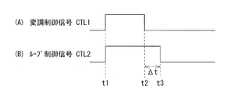
- FIG. 3shows an operation example of the signal generation unit 29, where (A) shows the waveform of the modulation control signal CTL1, and (B) shows the waveform of the loop control signal CTL2.
- the switches 23A and 23Bare turned off during a period in which the modulation control signal CTL1 is at a low level, and turned on in a period in which the modulation control signal CTL1 is at a high level.
- the phase synchronization unit 30performs a closed loop operation during a period in which the loop control signal CTL2 is at a low level, and performs an open loop operation in a period in which the loop control signal CTL2 is at a high level.
- the signal generation unit 29changes the loop control signal CTL2 from the low level to the high level in response to the rise.
- the signal generation unit 29sets the loop control signal CTL2 to the high level at the timing t3 when a predetermined time has elapsed from the falling timing t2 in response to the falling. From low to low.
- the signal generation unit 29generates the loop control signal CTL2 having a pulse width longer than that of the modulation control signal CTL1 by delaying the falling timing of the modulation control signal CTL1 by the shift amount ⁇ t.
- the phase synchronization unit 30performs an open loop operation in a period (period t1 to t3) corresponding to the period t1 to t2 in which the switches 23A and 23B are turned on.
- the rising timing of the loop control signal CTL2is equal to the rising timing of the modulation control signal CTL1, but the present invention is not limited to this.
- the rising timing of the loop control signal CTL2may be delayed by a circuit delay from the rising timing of the modulation control signal CTL1.
- the rising timing of the loop control signal CTL2is the modulation control signal CTL1 only for the time required for circuit operation such as the setup time. It may be later than the rise timing.
- the demodulator 26receives data D1 transmitted from the communication device 10 by performing a demodulation operation based on the signal Sin at the other end of the coil 21, and is configured using an ASK demodulator. Is.
- the demodulator 26supplies the data D1 to other blocks in the communication device 20.
- phase synchronizer 30 and the demodulator 26are operated based on the signal Sin at the other end of the coil 21, but the present invention is not limited to this.
- the phase synchronization unit 30 and the demodulation unit 26may be operated based on a signal at one end of the coil 21 or may be operated based on a signal between both ends of the coil 21.
- the communication device 20corresponds to a specific example of “communication device” in the present disclosure.
- the amplifiers 24A and 24B and the switches 23A and 23Bcorrespond to a specific example of “modulation unit” in the present disclosure.
- the communication control unit 28 and the signal generation unit 29correspond to a specific example of “control unit” in the present disclosure.
- the communication device 10transmits data D1 to the communication device 20 by ASK modulation. Specifically, in the communication device 10, first, the carrier signal generation unit 11 generates a carrier signal, and the data generation unit 12 generates data D1 to be transmitted.
- the modulation unit 13generates a signal SIG11 by modulating the carrier signal by ASK modulation using the data D1.
- the amplifier 14generates a signal SIG12 based on the signal SIG11.
- the coil 15generates a magnetic field based on the signal SIG12.
- the coil 21generates a signal SIG21 based on the magnetic field generated by the coil 15.
- the demodulator 26receives the data D1 transmitted from the communication device 10 by performing a demodulation operation based on the signal Sin at the other end of the coil 21.
- the communication device 20transmits data D2 to the communication device 10 by active load modulation. Specifically, first, during a period in which the communication device 10 transmits a carrier signal to the communication device 20, the communication control unit 28 generates the modulation control signal CTL1 based on the data D2. The signal generator 29 generates a loop control signal CTL2 based on the modulation control signal CTL1. The phase synchronization unit 30 selectively performs an open loop operation or a closed loop operation based on the loop control signal CTL2, and generates a signal SIG30 based on the signal Sin. The amplifier 24A amplifies the output signal SIG30 of the phase synchronization unit 30 and outputs the amplified signal.
- the amplifier 24Binverts and amplifies the output signal SIG30 of the phase synchronization unit 30, and outputs an inverted and amplified signal.
- the switches 23A and 23Bare turned on / off based on the modulation control signal CTL1. Thereby, the load seen from the communication apparatus 10 changes according to the data D2.
- the demodulator 17 of the communication device 10receives the data D2 transmitted from the communication device 20 by performing a demodulation operation based on the signal at the other end of the coil 15.
- the communication device 20transmits data D2 to the communication device 10 by so-called active load modulation.
- active load modulationwill be described in detail.
- the communication control unit 28turns on and off the switches 23A and 23B according to the data D2 during a period in which the communication device 10 transmits a carrier signal to the communication device 20.
- the switches 23A and 23Bare turned on, the output signal of the amplifier 24A is supplied to one end of the coil 21 and the output signal of the amplifier 24B is supplied to the other end of the coil 21.
- the coil 21generates a magnetic field.
- the coil 21 of the communication device 20generates a magnetic field during the period in which the communication device 10 transmits a carrier signal to the communication device 20, thereby greatly changing the magnetic field.
- the load viewed from the communication device 10can be greatly changed.
- the demodulator 17 of the communication device 10receives the data D2 transmitted from the communication device 20 by performing a demodulation operation based on the load change.
- the communication distancecan be extended, or the antennas (coils 15, 21) can be downsized.
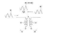
- FIG. 3schematically shows the operation of active load modulation.
- the coil 15 of the communication device 10generates a magnetic field based on the carrier signal W1
- the coil 21 of the communication device 20generates a magnetic field based on the signal W2 synchronized with the carrier signal in a period in which the switches 23A and 23B are turned on. Is generated.
- the demodulation unit 17 of the communication device 10performs a demodulation operation based on the combined signal W3 of the carrier signal W1 and the signal W2.
- This combined signal W3can be expressed as follows.
- the first term on the left siderepresents the carrier signal W1
- the second term on the left siderepresents the signal W2.
- the synthesized signal W3can be expressed using a sine wave synthesis theorem.
- the amplitude of this combined signal W3varies depending on the amplitude A of the carrier signal W1, the amplitude B of the signal W2, and the phase ⁇ . Therefore, depending on the situation, the amplitude of the synthesized signal W3 may be extremely small.
- the amplitude of the signal Sin at the other end of the coil 21is also reduced.
- the phase synchronization unit 30performs an open loop operation in a period (an open loop operation period P2 described later) corresponding to a period during which active load modulation is performed (a modulation period P1 described later). To control. Thereby, in the communication apparatus 20, even when the amplitude of the signal Sin becomes small due to the active load modulation, the possibility that the phase synchronization unit 30 malfunctions can be reduced.
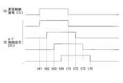
- FIG. 5shows an operation example of the communication system 1, (A) shows the waveform of the modulation control signal CTL1, (B) shows the waveform of the loop control signal CTL2, and (C) shows the signal Sin. Waveform is shown.
- the communication device 20performs active load modulation in the modulation period P1.
- the phase synchronization unit 30performs an open loop operation in the open loop operation period P2 corresponding to the modulation period P1. This operation will be described in detail below.
- the communication control unit 28 of the communication device 20sets the modulation control signal CTL1 to a low level (FIG. 5A). Thereby, the switches 23A and 23B are turned off. Therefore, the signal Sin corresponding to the carrier signal transmitted by the communication device 10 appears at the other end of the coil 21 (FIG. 5C). Further, the signal generator 29 sets the loop control signal CTL2 to a low level based on the modulation control signal CTL1 (FIG. 5B). Accordingly, the phase synchronization unit 30 performs a closed loop operation. That is, the phase synchronization unit 30 generates a signal SIG30 synchronized with the signal Sin based on the signal Sin.
- the communication control unit 28changes the modulation control signal CTL1 from the low level to the high level at the timing t11 (FIG. 5A).
- the switches 23A and 23Bare turned on, and the communication device 20 starts active load modulation.
- the signal generation unit 29changes the loop control signal CTL2 from the low level to the high level based on the modulation control signal CTL1 (FIG. 5B).
- the phase synchronization unit 30starts an open loop operation.
- the switch 33is turned off.
- the loop filter 34maintains the output voltage, the frequency of the output signal SIG30 of the phase synchronization unit 30 is maintained.
- the communication control unit 28changes the modulation control signal CTL1 from the high level to the low level at timing t12 (FIG. 5A).
- the switches 23A and 23Bare turned off.
- the amplitude of the signal Sinincreases with a predetermined time constant and approaches the amplitude before the timing t11 (FIG. 5C).
- the signal generation unit 29changes the loop control signal CTL2 from the high level to the low level at timing t13 when the time corresponding to the shift amount ⁇ t has elapsed from timing t12 (FIG. 5B).
- the phase synchronization unit 30starts a closed loop operation.
- the communication device 20transmits data D2 to the communication device 10 by repeating such an operation.
- phase synchronization unit 30since the phase synchronization unit 30 performs the open loop operation in the open loop operation period P2 corresponding to the modulation period P1, the possibility that the phase synchronization unit 30 malfunctions can be reduced. it can.
- the phase synchronization unit 30may malfunction if the amplitude of the signal Sin decreases during the modulation period P1. Specifically, when the amplitude of the signal Sin is extremely small, the PFD 31 of the phase synchronization unit 30 cannot detect the transition of the signal Sin, and thus cannot perform the phase comparison operation. As a result, the output voltage of the loop filter 34 gradually departs from the desired voltage, and as a result, the frequency of the signal SIG30 deviates from the desired frequency.
- the phase synchronization unit 30may not be able to return the frequency of the signal SIG30 to a desired frequency even when the modulation period P1 ends and the amplitude of the signal Sin increases. Further, when the frequency is shifted in this manner, the frequency of the radio signal to be used may be out of the frequency band that can be used in short-range wireless communication, and the standard for short-range wireless communication may not be satisfied.
- the phase synchronization unit 30performs the open loop operation in the open loop operation period P2 corresponding to the modulation period P1.
- the output voltage of the loop filter 34is maintained because the switch 33 of the phase synchronization unit 30 is in the OFF state.
- the frequency of the signal SIG30is maintained. Therefore, after that, when the phase synchronization unit 30 starts the closed loop operation, the phase synchronization unit 30 can more reliably synchronize the signal SIG30 with the signal Sin.
- the possibility that the phase synchronization unit 30 malfunctionscan be reduced. As a result, communication quality can be improved in the communication system 1.
- the phase synchronization unit 30when the signal generation unit 29 is not provided and the phase synchronization unit 30 is configured to selectively perform an open loop operation or a closed loop operation based on the modulation control signal CTL1, Closed loop operation is started at t12. At this time, since the amplitude of the signal Sin is still small immediately after the timing t12, the phase synchronization unit 30 may malfunction.
- the end timing of the open loop operation period P2is made later than the end timing of the modulation period P1.
- the signal generation unit 29generates the loop control signal CTL2 by delaying the falling timing of the modulation control signal CTL1 by the shift amount ⁇ t.
- the phase synchronization unit 30starts the closed loop operation at the timing t13 when the amplitude of the signal Sin increases, so that the possibility that the phase synchronization unit 30 malfunctions can be reduced. As a result, communication quality can be improved in the communication system 1.
- FIG. 6shows another example of the operation of the communication system 1.
- Ashows the waveform of the modulation control signal CTL1
- Bshows the waveform of the loop control signal CTL2
- Cshows the signal Sin. The waveform is shown.
- the communication control unit 28 of the communication device 20sets the modulation control signal CTL1 to a low level (FIG. 6A), and the signal generation unit 29 performs loop control.
- the signal CTL2is set to a low level (FIG. 6B).
- a signal Sin corresponding to the carrier signal transmitted by the communication device 10appears at the other end of the coil 21 (FIG. 6C).
- the communication control unit 28changes the modulation control signal CTL1 from the low level to the high level at the timing t21 (FIG. 6A). Thereby, the switches 23A and 23B are turned on, and the communication device 20 starts active load modulation. At the same time, the signal generation unit 29 changes the loop control signal CTL2 from the low level to the high level based on the modulation control signal CTL1 (FIG. 6B). As a result, the phase synchronization unit 30 starts an open loop operation. In this example, when the switches 23A and 23B are turned on, the carrier signal transmitted by the communication device 10 and the signal SIG30 are combined, and the amplitude of the signal Sin increases with a predetermined time constant (FIG. 6 ( C)). Then, the amplitude of the signal Sin is kept large until the timing t22.
- the communication control unit 28changes the modulation control signal CTL1 from the high level to the low level at timing t22 (FIG. 6A).
- the switches 23A and 23Bare turned off.
- the amplitude of the signal Sindecreases with a predetermined time constant (FIG. 6C).
- the amplitude of the signal Sinbecomes extremely small transiently as shown in the waveform W1, and then gradually increases and approaches the amplitude before the timing t21.
- the signal generation unit 29changes the loop control signal CTL2 from the high level to the low level at timing t23 when the time corresponding to the shift amount ⁇ t has elapsed from timing t22 (FIG. 6B).
- the phase synchronization unit 30starts a closed loop operation.
- the communication device 20transmits data D2 to the communication device 10 by repeating such an operation.
- the amplitude of the signal Sinincreases during the modulation period P1, and decreases after the modulation period P1 ends.
- the amplitude of the signal Sinbecomes transiently extremely small.
- the end timing of the open loop operation period P2is set to timing t23 after the waveform W1 appears.
- the phase synchronization unit 30does not perform a closed-loop operation during a period in which the amplitude of the signal Sin is extremely small, so that the possibility of malfunctioning can be reduced.
- communication qualitycan be improved in the communication system 1.
- the signal generation unit 29generates the loop control signal CTL2 by delaying the falling timing of the modulation control signal CTL1 by the shift amount ⁇ t.
- the communication distancecan be extended by increasing the shift amount ⁇ t.
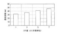
- FIG. 7shows the communication characteristics of the communication system 1.
- the horizontal axisindicates the shift amount ⁇ t, and the vertical axis indicates the communication distance.
- the amplitude A of the carrier signal W1 shown in FIG. 4is small. Therefore, the amplitude of the composite signal W3 changes according to the communication distance.
- the possibility that the phase synchronization unit 30 malfunctionscan be reduced by increasing the shift amount ⁇ t.
- the communication distancecan be extended by increasing the shift amount ⁇ t.
- phase synchronization unitsince the phase synchronization unit performs the open loop operation in the open loop operation period corresponding to the load modulation, it is possible to reduce the possibility that the phase synchronization unit malfunctions. Communication quality can be improved.
- the end timing of the open loop operation periodis made later than the end timing of the modulation period, so that the possibility that the phase synchronization unit malfunctions can be reduced, so that the communication quality can be improved.
- the communication distancecan be extended by reducing the possibility that the phase synchronization unit malfunctions in this way.
- the signal generation unit 29generates the loop control signal CTL2 by delaying the falling timing of the modulation control signal CTL1 by the shift amount ⁇ t.
- the shift amount ⁇ tmay be configured to be changeable as shown in FIG.
- the signal generation unit 29A according to this modificationcan set the falling timing of the loop control signal CTL2 to any one of timings t31 to t38.
- the falling timing of the loop control signal CTL2can be set to eight ways, but is not limited to this, and may be seven or less, or nine or more.
- the shift amount ⁇ tis fixed.
- the shift amount ⁇ tis not limited to this.
- the shift amount ⁇ tmay be changed according to the communication state. Below, this modification is demonstrated in detail.
- FIG. 9illustrates a configuration example of the communication system 1B according to the present modification.
- the communication system 1Bincludes a communication device 20B.
- the communication device 20Bincludes a demodulator 26B and a signal generator 29B.
- the demodulator 26Bperforms a demodulation operation based on the signal Sin at the other end of the coil 21, and determines a standard (communication standard SP) to which the communication device 10 complies.
- a standardcommunication standard SP
- the modulation degree of the signal transmitted from the communication device 10can be used. That is, as described above, the communication device 10 conforms to any one of various standards such as Type A standard, Type B standard, FeliCa standard, ISO 15693 standard, and the modulation unit 13 of the communication device 10 ASK modulation is performed with a modulation degree corresponding to the standard that is compliant. Therefore, the demodulator 26B can determine the standard (communication standard SP) to which the communication device 10 is based on the modulation degree of the signal transmitted from the communication device 10.
- the demodulator 26Bmay determine the communication standard SP based on other characteristics of the signal (coding, bit rate, subcarrier), and the like. For example, when the data D1 transmitted by the communication device 10 includes information according to the communication standard SP, the demodulation unit 26B may determine the communication standard SP based on the information.
- the signal generation unit 29Bis configured to be able to change the shift amount ⁇ t, and sets the shift amount ⁇ t based on the communication standard SP. is there.
- FIG. 14shows an operation example of the communication system 2B.
- the communication device 10transmits data D1 to the communication device 20B.
- the communication device 20Bresponds by transmitting the data D2 to the communication device 10. This operation will be described in detail below.
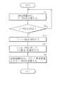
- the communication device 10transmits data D1 to the communication device 20B by ASK modulation (step S1).
- the demodulation unit 26B of the communication device 20Bconfirms whether or not the data D1 has been received (step S2).
- the data generator 27 of the communication device 20Bgenerates data D2 for responding to the communication device 10, and proceeds to step S3. If the demodulator 26B cannot receive the data D1, the process returns to step S1, and steps S1 and S2 are repeated until the data is received.
- the demodulator 27B of the communication device 20Bdetermines the communication standard SP (step S3). Then, the signal generation unit 29B of the communication device 20B sets the shift amount ⁇ t based on the communication standard SP determined in step S3 (step S4). Next, the communication device 20B transmits data D2 to the communication device 10 by active load modulation (step S5).
- the shift amount ⁇ tis set based on the communication standard SP, the degree of freedom in setting the shift amount ⁇ t can be increased.
- the communication standard SPis a standard used for an application with a long communication distance
- the shift amount ⁇ tcan be set to a large value so that the communicable distance becomes long.
- communication qualitycan be improved in the communication system 2B.
- the shift amount ⁇ tis set based on the communication standard SP, but the present invention is not limited to this.
- the shift amount ⁇ tmay be set based on the bit rate BR.
- the communication system 1Cincludes a communication device 20C.
- the communication device 20Cincludes a demodulation unit 26C and a signal generation unit 29C.
- the demodulator 26Cperforms a demodulating operation based on the signal Sin at the other end of the coil 21, and determines the bit rate BR when performing communication between the communication device 10 and the communication device 20C.
- the bit rate BRcan be acquired by detecting the frequency of the signal transmitted from the communication device 10 as the determination method.
- the demodulator 26Cmay determine the bit rate BR based on the information.
- the signal generation unit 29Csets the shift amount ⁇ t based on the bit rate BR.
- FIG. 11shows an operation example of the communication system 1C.
- the communication device 10transmits data D1 to the communication device 20C by ASK modulation (step S1), and the demodulation unit 26C of the communication device 20C It is confirmed whether or not the data D1 has been received (step S2).
- the demodulator 26C of the communication device 20Cdetermines the bit rate BR (step S13).
- the signal generation unit 29C of the communication device 20Csets the shift amount ⁇ t based on the bit rate BR determined in step S13 (step S14).
- the communication device 20Ctransmits data D2 to the communication device 10 by active load modulation as in the communication system 1B (FIG. 10) (step S5).
- the degree of freedom in setting the shift amount ⁇ tcan be increased. Specifically, for example, when the bit rate BR is high, the time corresponding to each transmission symbol is shortened, so it is desirable to set the shift amount ⁇ t to a small value. As a result, communication quality can be improved in the communication system 2C.
- the shift amount ⁇ tis set based on the bit rate BR, but the present invention is not limited to this.
- the shift amount ⁇ tmay be set based on the voltage amplitude of the signal Sin.
- FIG. 12shows a configuration example of the communication system 1D.
- the communication system 1Dincludes a communication device 20D.
- the communication device 20Dincludes an amplitude detection unit 25D and a signal generation unit 29D.
- the amplitude detector 25Ddetects the amplitude value Vsw of the signal Sin based on the signal Sin.
- the signal generation unit 29Dsets the shift amount ⁇ t based on the amplitude value Vsw.
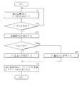
- FIG. 13shows an operation example of the communication system 1D.
- the communication device 10transmits data D1 to the communication device 20D by ASK modulation (step S1), and the demodulation unit 26 of the communication device 20D It is confirmed whether or not the data D1 has been received (step S2).
- the amplitude detector 25D of the communication device 20Ddetects the amplitude value Vsw of the signal Sin (step S23).
- the signal generation unit 29D of the communication device 20Dcompares the amplitude value Vsw detected in step S23 with a predetermined threshold value Vth (step S24).
- the signal generation unit 29Dsets the shift amount ⁇ t to the shift amount ⁇ t1 (step S25).
- the signal generation unit 29Dsets the shift amount ⁇ t to the shift amount ⁇ t2 (step S26).
- the communication device 20Dtransmits data D2 to the communication device 10 by active load modulation (step S5).
- the degree of freedom in setting the shift amount ⁇ tcan be increased.
- the amplitude value Vsw of the signal Sinis small, it is desirable to set the shift amount ⁇ t to a large value because the communication distance between the communication device 10 and the communication device 20D is long. As a result, communication quality can be improved in the communication system 2D.
- the amplitude value Vsw of the signal Sinis compared with one threshold value Vth.
- the present inventionis not limited to this, and may be compared with a plurality of threshold values. Thereby, the shift amount ⁇ t can be set more finely. Further, when the amplitude value Vsw of the signal Sin is sufficiently large, the shift amount ⁇ t may be set to 0 (zero).
- the shift amount ⁇ tmay be set based on two or more of the communication standard SP, the bit rate BR, and the amplitude value Vsw of the signal Sin.
- the communication system 2includes a communication device 40.
- the communication device 40has a signal generation unit 49.
- the signal generation unit 49generates a loop control signal CTL2 based on the modulation control signal CTL1, and supplies the loop control signal CTL2 to the phase synchronization unit 30.
- FIG. 14shows an example of the operation of the signal generator 49, (A) shows the waveform of the modulation control signal CTL1, and (B) shows the waveform of the loop control signal CTL2.
- the signal generation unit 49changes the loop control signal CTL2 from the low level to the high level at the timing t42 when a predetermined time has elapsed from the rising timing t41.
- the signal generation unit 49sets the loop control signal CTL2 to the high level at the timing t44 when a predetermined time has elapsed from the falling timing t43 in response to the falling. From low to low. In other words, the signal generation unit 49 generates the loop control signal CTL2 by delaying the rising timing and falling timing of the modulation control signal CTL1 by the shift amount ⁇ t.
- FIG. 15illustrates an operation example of the communication system 2, in which (A) shows the waveform of the modulation control signal CTL1, (B) shows the waveform of the loop control signal CTL2, and (C) shows the signal Sin. Waveform is shown.
- FIG. 15corresponds to Operation Example 1 (FIG. 5) according to the first embodiment.
- the communication control unit 28changes the modulation control signal CTL1 from the low level to the high level at the timing t51 (FIG. 15A). Thereby, the switches 23A and 23B are turned on, and the communication device 40 starts active load modulation. As a result, the carrier signal transmitted by the communication device 10 and the signal SIG30 are combined, and the amplitude of the signal Sin decreases with a predetermined time constant (FIG. 15C). The amplitude of this signal Sin is kept small until timing t53.
- the signal generation unit 49changes the loop control signal CTL2 from the low level to the high level at the timing t52 when the time corresponding to the shift amount ⁇ t has elapsed from the timing t51 (FIG. 15B).
- the phase synchronization unit 30starts an open loop operation.
- the switch 33is turned off.
- the loop filter 34maintains the output voltage, the frequency of the output signal SIG30 of the phase synchronization unit 30 is maintained.
- the communication control unit 28changes the modulation control signal CTL1 from the high level to the low level at timing t53 (FIG. 15A).
- the switches 23A and 23Bare turned off.
- the amplitude of the signal Sinincreases with a predetermined time constant and approaches the amplitude before the timing t51 (FIG. 15C).
- the signal generation unit 49changes the loop control signal CTL2 from the high level to the low level at timing t54 when the time corresponding to the shift amount ⁇ t has elapsed from timing t53 (FIG. 15B). As a result, the phase synchronization unit 30 starts a closed loop operation.
- the communication device 40transmits data D2 to the communication device 10 by repeating such an operation.
- the start timing of the open loop operation period P2is made later than the start timing of the modulation period P1.
- the phase synchronization unit 30can perform a closed-loop operation in the period from the timing t51 to t52. That is, during this period, the amplitude of the signal Sin gradually decreases, but the amplitude is an amplitude with which the phase synchronization unit 30 can perform a closed loop operation. Therefore, in the communication system 2, the phase synchronization unit 30 is operated during this period. Thereby, since the period for which the phase synchronization unit 30 performs the closed loop operation can be extended, the signal SIG30 can be more reliably synchronized with the signal Sin. As a result, communication quality can be improved in the communication system 2.
- the start timing of the open loop operation periodis delayed from the start timing of the modulation period, it is possible to extend the period during which the phase synchronization unit performs the closed loop operation, thereby improving communication quality. be able to.
- Other effectsare the same as in the case of the first embodiment.
- the signal generation unit 49generates the loop control signal CTL2 by delaying the rising timing and falling timing of the modulation control signal CTL1 by the shift amount ⁇ t.
- This shift amount ⁇ tmay be configured to be changeable as shown in FIG.
- the signal generation unit 49Asets the rising timing of the loop control signal CTL2 to any one of timings t61 to 64, and sets the falling timing of the loop control signal CTL2 to any one of timings t71 to t74. It can be set.
- the rising timing and falling timing of the loop control signal CTL2can be set in four ways. However, the present invention is not limited to this and may be three or less, or may be five or more.
- the signal generation unit 48generates the loop control signal CTL2 by delaying the rising timing and the falling timing of the modulation control signal CTL1 by the shift amount ⁇ t.
- the present inventionis not limited to this. Is not to be done.
- the loop control signal CTL2may be generated by delaying the rising timing of the modulation control signal CTL1 by the shift amount ⁇ ta and delaying the falling timing by the shift amount ⁇ tb.
- the degree of freedom of operationcan be increased by making the shift amount ⁇ ta at the time of rising different from the shift amount ⁇ tb at the time of falling.
- phase synchronization unitthat generates a second signal based on a first signal received from a communication partner by selectively performing a closed-loop operation or an open-loop operation;
- a modulatorconfigured to be capable of modulating the first signal based on the second signal;
- a control unitthat controls operations of the phase synchronization unit and the modulation unit.
- the control unitcauses the modulation unit to modulate the first signal in a modulation period, and performs an open loop operation on the phase synchronization unit in an open loop operation period corresponding to the modulation period.
- the communication device according to (1)wherein operation is performed.
- the control unitgenerates a modulation control signal that becomes a first logic level in the modulation period and becomes a second logic level in a period other than the modulation period, and based on the modulation control signal, Generating a loop control signal that is at a third logic level during the open loop operation period and that is at a fourth logic level during a period other than the open loop operation period;
- the modulation unitmodulates the first signal based on the modulation control signal,
- the communication deviceaccording to (2) or (3), wherein the phase synchronization unit selectively performs the closed loop operation or the open loop operation based on the loop control signal.
- the control unitgenerates the loop control signal by delaying a first transition timing of the modulation control signal from the first logic level to the second logic level.
- the communication device described. (6)The communication device according to (5), wherein the control unit determines an amount by which the first transition timing is delayed based on a communication method with the communication partner. (7) The communication device according to (5) or (6), wherein the control unit determines an amount of delaying the first transition timing based on a communication rate in communication with the communication partner. (8) The communication device according to any one of (5) to (7), wherein the control unit determines an amount by which the first transition timing is delayed based on a signal amplitude of the first signal. (9) The control unit further generates the loop control signal by delaying a second transition timing of the modulation control signal from the second logic level to the first logic level. ) To (8).
- the modulation unitincludes a switch, The phase synchronization unit receives the first signal from the communication partner via a coil, The communication device according to any one of (1) to (9), wherein the switch supplies the second signal to the coil by being turned on. (11) By causing the phase synchronization unit to selectively perform a closed loop operation or an open loop operation, the second signal is generated based on the first signal received from the communication partner, A communication method in which a modulation unit modulates the first signal based on the second signal.
- a first communication devicethat transmits a first signal
- a second communication deviceThe second communication device is: A phase synchronization unit that generates a second signal based on the first signal received from the first communication device by selectively performing a closed-loop operation or an open-loop operation; A modulator configured to be capable of modulating the first signal based on the second signal; And a control unit that controls operations of the phase synchronization unit and the modulation unit.
Landscapes
- Engineering & Computer Science (AREA)
- Computer Networks & Wireless Communication (AREA)
- Signal Processing (AREA)
- Physics & Mathematics (AREA)
- Electromagnetism (AREA)
- Near-Field Transmission Systems (AREA)
Abstract
Description
Translated fromJapanese本開示は、近距離無線通信(NFC;Near Field Communication)において用いられる通信装置、およびそのような通信装置に用いられる通信方法、ならびにそのような通信装置を備えた通信システムに関する。The present disclosure relates to a communication device used in near field communication (NFC), a communication method used in such a communication device, and a communication system including such a communication device.
近距離無線通信は、交通系や課金、認証等でアジア圏を中心に普及が進んでいる技術であり、国際標準規格として承認された技術である。近距離無線通信の規格(以下NFC規格ともいう)は、例えばTypeA規格、TypeB規格、FeliCa(登録商標)規格、ISO15693規格などの様々な規格と、いわゆる上位互換としての互換性を有している。すなわち、例えば、NFC規格に準拠しているリーダライタやカードは、これらの全ての規格にも準拠することとなる。Near field communication is a technology that is spreading mainly in Asia due to transportation, billing, authentication, etc., and is a technology approved as an international standard. Short-range wireless communication standards (hereinafter also referred to as NFC standards) have compatibility as a so-called upward compatibility with various standards such as Type A standards, Type B standards, FeliCa (registered trademark) standards, and ISO 15693 standards. . That is, for example, a reader / writer or card that conforms to the NFC standard also conforms to all these standards.
近距離無線通信では、例えば、リーダライタは、カードに対してASK(Amplitude Shift Keying)変調によりデータを送信し、カードは、リーダライタに対して、負荷変調によりデータを送信する。例えば、特許文献1,2には、負荷変調(パッシブ負荷変調)により通信を行うことができる通信装置が開示されている。In short-range wireless communication, for example, the reader / writer transmits data to the card by ASK (Amplitude Shift Keying) modulation, and the card transmits data to the reader / writer by load modulation. For example,
ところで、電子回路では、例えば特許文献3に示したように、位相同期回路(PLL;Phase Locked Loop)がしばしば用いられる。By the way, in an electronic circuit, as shown in
ところで、一般に、通信においては、通信品質を高めることが望まれており、通信品質のさらなる向上が期待されている。Incidentally, in general, in communication, it is desired to improve communication quality, and further improvement in communication quality is expected.
通信品質を高めることができる通信装置、通信方法、および通信システムを提供することが望ましい。It is desirable to provide a communication device, a communication method, and a communication system that can improve communication quality.
本開示の一実施の形態における通信装置は、位相同期部と、変調部と、制御部とを備えている。位相同期部は、閉ループ動作または開ループ動作を選択的に行うことにより、通信相手から受け取った第1の信号に基づいて第2の信号を生成するものである。変調部は、第2の信号に基づいて第1の信号を変調可能に構成されたものである。制御部は、位相同期部および変調部の動作を制御するものである。The communication device according to an embodiment of the present disclosure includes a phase synchronization unit, a modulation unit, and a control unit. The phase synchronization unit generates a second signal based on a first signal received from a communication partner by selectively performing a closed loop operation or an open loop operation. The modulation unit is configured to be able to modulate the first signal based on the second signal. The control unit controls operations of the phase synchronization unit and the modulation unit.
本開示の一実施の形態における通信方法は、位相同期部に対して、閉ループ動作または開ループ動作を選択的に行わせることにより、通信相手から受け取った第1の信号に基づいて第2の信号を生成させ、変調部に対して、第2の信号に基づいて第1の信号を変調させるものである。In the communication method according to the embodiment of the present disclosure, the second signal is generated based on the first signal received from the communication partner by selectively causing the phase synchronization unit to perform the closed-loop operation or the open-loop operation. And the modulation unit modulates the first signal based on the second signal.
本開示の一実施の形態における通信システムは、第1の通信装置と、第2の通信装置とを備えている。第1の通信装置は、第1の信号を送信するものである。第2の通信装置は、位相同期部と、変調部と、制御部とを有している。位相同期部は、閉ループ動作または開ループ動作を選択的に行うことにより、第1の通信装置から受け取った第1の信号に基づいて第2の信号を生成するものである。変調部は、第2の信号に基づいて第1の信号を変調可能に構成されたものである。制御部は、位相同期部および変調部の動作を制御するものである。The communication system according to an embodiment of the present disclosure includes a first communication device and a second communication device. The first communication device transmits the first signal. The second communication device includes a phase synchronization unit, a modulation unit, and a control unit. The phase synchronization unit generates a second signal based on the first signal received from the first communication device by selectively performing a closed loop operation or an open loop operation. The modulation unit is configured to be able to modulate the first signal based on the second signal. The control unit controls operations of the phase synchronization unit and the modulation unit.
本開示の一実施の形態における通信装置、通信方法、および通信システムでは、通信相手から受け取った第1の信号に基づいて、位相同期部により第2の信号が生成される。そして、この第2の信号に基づいて、第1の信号が変調される。上記位相同期部では、閉ループ動作または開ループ動作が選択的に行われる。In the communication device, the communication method, and the communication system according to the embodiment of the present disclosure, the phase synchronization unit generates the second signal based on the first signal received from the communication partner. Based on the second signal, the first signal is modulated. In the phase synchronization unit, a closed loop operation or an open loop operation is selectively performed.
本開示の一実施の形態における通信装置、通信方法、および通信システムによれば、位相同期部が、閉ループ動作または開ループ動作を選択的に行うようにしたので、通信品質を高めることができる。なお、ここに記載された効果は必ずしも限定されるものではなく、本開示中に記載されたいずれの効果があってもよい。According to the communication device, the communication method, and the communication system according to the embodiment of the present disclosure, the phase synchronization unit selectively performs the closed loop operation or the open loop operation, so that the communication quality can be improved. In addition, the effect described here is not necessarily limited, and there may be any effect described in the present disclosure.
以下、本開示の実施の形態について、図面を参照して詳細に説明する。なお、説明は以下の順序で行う。
1.第1の実施の形態
2.第2の実施の形態Hereinafter, embodiments of the present disclosure will be described in detail with reference to the drawings. The description will be given in the following order.
1.
<1.第1の実施の形態>
[構成例]
図1は、第1の実施の形態に係る通信装置を備えた通信システム1の一構成例を表すものである。通信システム1は、近距離無線通信により通信を行うものである。なお、本開示の実施の形態に係る通信方法は、本実施の形態により具現化されるので、併せて説明する。通信システム1は、通信装置10と、通信装置20とを備えている。<1. First Embodiment>
[Configuration example]
FIG. 1 illustrates a configuration example of a
通信装置10および通信装置20は、磁界を介して互いに通信を行うものである。具体的には、通信システム1では、通信装置10のコイル15(後述)と通信装置20のコイル21(後述)とが磁界を介して結合することにより、電磁誘導によりデータを送受信するようになっている。その際、通信装置10は、ASK変調により、通信装置20に対してデータを送信し、通信装置20は、いわゆるアクティブ負荷変調により、通信装置10に対してデータを送信するようになっている。通信装置10は、例えばリーダライタに適用されるものであり、TypeA規格、TypeB規格、FeliCa規格、ISO15693規格などの様々な規格のうちのいずれか一つに準拠している。通信装置20は、例えばカードに適用されるものであり、これらの規格の上位互換であるNFC規格に準拠している。The
通信装置10は、キャリア信号生成部11と、データ生成部12と、変調部13と、アンプ14と、コイル15と、キャパシタ16と、復調部17とを有している。The
キャリア信号生成部11は、キャリア信号を生成するものである。キャリア信号の周波数は、例えば、13.56MHzである。データ生成部12は、送信すべきデータD1を生成するものである。The
変調部13は、キャリア信号をデータD1を用いてASK変調により変調することにより、信号SIG11を生成するものである。The modulating
アンプ14は、信号SIG11に基づいて信号SIG12を生成し、その信号SIG12を第1の出力端子および第2の出力端子の端子間信号として出力するものである。アンプ14の第1の出力端子は、コイル15の一端およびキャパシタ16の一端に接続されている。アンプ14の第2の出力端子は、コイル15の他端およびキャパシタ16の他端に接続されている。The
コイル15は、信号SIG12に基づいて磁界を発生させるものであり、通信装置20のコイル21(後述)と磁界を介して結合するものである。コイル15の一端は、アンプ14の第1の出力端子およびキャパシタ16の一端に接続され、他端は、アンプ14の第2の出力端子およびキャパシタ16の他端に接続されている。キャパシタ16の一端は、コイル15の一端およびアンプ14の第1の出力端子に接続され、他端は、コイル15の他端およびアンプ14の第2の出力端子に接続されている。The
復調部17は、コイル15の他端における信号に基づいて復調動作を行うことにより、通信装置20から送信されたデータD2を受け取るものであり、例えば、いわゆるI/Q(In-phase/Quadrature)復調器を用いて構成されるものである。通信システム1では、通信装置20は、通信装置10にデータを送信する際、負荷変調により通信を行う。具体的には、通信装置10が通信装置20に対してキャリア信号を送信している期間において、通信装置20の通信制御部28(後述)が、送信すべきデータD2に応じて、通信装置10からみた負荷を変化させる。この負荷の変化は、通信装置10において、例えば、コイル15の他端における電圧信号の振幅や位相の変化として現れる。復調部17は、コイル15の他端における電圧信号の振幅や位相を検出することにより、通信装置20から送信されたデータD2を受け取る。そして、復調部17は、このデータD2を、通信装置10内の他のブロックに供給するようになっている。The
なお、この例では、復調部17は、コイル15の他端における信号に基づいて動作するようにしたが、これに限定されるものではない。例えば、復調部17は、コイル15の一端における信号に基づいて動作するようにしてもよいし、コイル15の両端間の信号に基づいて動作するようにしてもよい。In this example, the
通信装置20は、コイル21と、キャパシタ22と、位相同期部30と、アンプ24A,24Bと、スイッチ23A,23Bと、データ生成部27と、通信制御部28と、信号生成部29と、復調部26とを有している。The
コイル21は、通信装置10のコイル15と磁界を介して結合するものであり、電磁誘導により、通信装置10における信号SIG12に対応する信号SIG21を生成するものである。コイル21の一端は、キャパシタ22の一端およびスイッチ23Aの一端に接続され、他端は、キャパシタ22の他端およびスイッチ23Bの一端に接続されている。キャパシタ22の一端は、コイル21の一端およびスイッチ23Aの一端に接続され、他端は、コイル21の他端およびスイッチ23Bの一端に接続されているThe
位相同期部30は、コイル21の他端における信号Sinに基づいて、信号SIG30を生成するものであり、PLL(Phase Locked Loop)を用いて構成されるものである。The
図2は、位相同期部30の一構成例を表すものである。位相同期部30は、PFD(Phase Frequency Detector)31と、チャージポンプ32と、スイッチ33と、ループフィルタ34と、VCO(Voltage Controlled Oscillator)35とを有している。FIG. 2 shows a configuration example of the
PFD31は、信号Sinの位相と、VCO35から出力された信号SIG30の位相とを比較するものである。チャージポンプ32は、PFD31における比較結果に基づいて、選択的に、ループフィルタ34に対して電流を流し、またはループフィルタ34から電流をシンクするものである。チャージポンプ32の出力端子は、スイッチ33を介してループフィルタ34の入力端子に接続されている。スイッチ33は、オン状態になることによりチャージポンプ32の出力端子とループフィルタ34の入力端子とを互いに接続するものであり、ループ制御信号CT2に基づいてオンオフするものである。ループフィルタ34は、位相同期部30におけるループ応答特性を定めるためのものであり、入力端子は、スイッチ33を介してチャージポンプ32の出力端子に接続され、出力端子は、VCO35の入力端子に接続されている。VCO35は、ループフィルタ34の出力電圧に応じた周波数で発振することにより、信号SIG30を生成するものである。The
この構成により、位相同期部30は、信号Sinに基づいて、信号SIG30を生成する。その際、位相同期部30は、ループ制御信号CTL2に基づいて、開ループ動作または閉ループ動作を選択的に行うことができるようになっている。With this configuration, the
アンプ24A(図1)は、信号SIG30を増幅し、増幅した信号を出力するものである。アンプ24Bは、信号SIG30を反転増幅し、反転増幅した信号を出力するものである。The
スイッチ23Aの一端は、コイル21の一端およびキャパシタ22の一端に接続され、他端はアンプ24Aの出力端子に接続されている。スイッチ23Bの一端は、コイル21の他端およびキャパシタ22の他端に接続され、他端はアンプ24Bの出力端子に接続されている。スイッチ23A,23Bは、変調制御信号CTL1に基づいてオンオフするようになっている。One end of the
この構成により、通信装置20では、変調制御信号CTL1に基づいてスイッチ23A,23Bをオンオフさせることにより、アクティブ負荷変調を行うようになっている。With this configuration, the
データ生成部27は、送信すべきデータD2を生成し、そのデータD2を通信制御部28に供給するものである。通信制御部28は、データD2に基づいて、変調制御信号CTL1を生成し、その変調制御信号CTL1をスイッチ23A,23Bに供給するとともに、信号生成部29に供給するものである。The
信号生成部29は、変調制御信号CTL1に基づいてループ制御信号CTL2を生成し、そのループ制御信号CTL2を位相同期部30に供給するものである。The
図3は、信号生成部29の一動作例を表すものであり、(A)は変調制御信号CTL1の波形を示し、(B)はループ制御信号CTL2の波形を示す。この例では、スイッチ23A,23Bは、変調制御信号CTL1が低レベルである期間においてオフ状態になり、変調制御信号CTL1が高レベルである期間においてオン状態になる。また、位相同期部30は、ループ制御信号CTL2が低レベルである期間において閉ループ動作を行い、ループ制御信号CTL2が高レベルである期間において開ループ動作を行う。FIG. 3 shows an operation example of the
タイミングt1において変調制御信号CTL1が立ち上がると、信号生成部29は、この立ち上がりに応じて、ループ制御信号CTL2を低レベルから高レベルに変化させる。そして、タイミングt2において変調制御信号CTL1が立ち下がると、信号生成部29は、この立ち下がりに応じて、その立ち下がりタイミングt2から所定の時間が経過したタイミングt3において、ループ制御信号CTL2を高レベルから低レベルに変化させる。言い換えれば、信号生成部29は、変調制御信号CTL1の立ち下がりタイミングをシフト量Δt分だけ遅らせることにより、変調制御信号CTL1よりもパルス幅が長いループ制御信号CTL2を生成する。これにより、位相同期部30は、スイッチ23A,23Bがオン状態になるタイミングt1~t2の期間に対応する期間(タイミングt1~t3の期間)において、開ループ動作を行うようになっている。When the modulation control signal CTL1 rises at timing t1, the
なお、この例では、ループ制御信号CTL2の立ち上がりタイミングは、変調制御信号CTL1の立ち上がりタイミングと等しくしたが、これに限定されるものではない。例えば、例えば、ループ制御信号CTL2の立ち上がりタイミングは、変調制御信号CTL1の立ち上がりタイミングよりも、回路遅延分だけ遅くてもよい。また、例えば、信号生成部29を、図示しないクロック信号により動作するように構成した場合には、ループ制御信号CTL2の立ち上がりタイミングは、セットアップタイムなどの回路動作に必要な時間だけ、変調制御信号CTL1の立ち上がりタイミングよりも遅くてもよい。In this example, the rising timing of the loop control signal CTL2 is equal to the rising timing of the modulation control signal CTL1, but the present invention is not limited to this. For example, for example, the rising timing of the loop control signal CTL2 may be delayed by a circuit delay from the rising timing of the modulation control signal CTL1. Further, for example, when the
復調部26(図1)は、コイル21の他端における信号Sinに基づいて復調動作を行うことにより、通信装置10から送信されたデータD1を受け取るものであり、ASK復調器を用いて構成されるものである。そして、復調部26は、このデータD1を、通信装置20内の他のブロックに供給するようになっている。The demodulator 26 (FIG. 1) receives data D1 transmitted from the
なお、この例では、位相同期部30および復調部26は、コイル21の他端における信号Sinに基づいて動作するようにしたが、これに限定されるものではない。例えば、位相同期部30および復調部26は、コイル21の一端における信号に基づいて動作するようにしてもよいし、コイル21の両端間の信号に基づいて動作するようにしてもよい。In this example, the
ここで、通信装置20は、本開示における「通信装置」の一具体例に対応する。アンプ24A,24B、およびスイッチ23A,23Bは、本開示における「変調部」の一具体例に対応する。通信制御部28および信号生成部29は、本開示における「制御部」の一具体例に対応する。Here, the
[動作および作用]
続いて、本実施の形態の通信システム1の動作および作用について説明する。[Operation and Action]
Next, the operation and action of the
(全体動作概要)
まず、図1を参照して、通信システム1の全体動作概要を説明する。(Overview of overall operation)
First, an overall operation overview of the
通信装置10は、ASK変調により、通信装置20に対してデータD1を送信する。具体的には、まず、通信装置10では、キャリア信号生成部11がキャリア信号を生成し、データ生成部12が送信すべきデータD1を生成する。変調部13は、キャリア信号を、データD1を用いてASK変調により変調することにより、信号SIG11を生成する。アンプ14は、信号SIG11に基づいて信号SIG12を生成する。コイル15は、信号SIG12に基づいて磁界を発生させる。通信装置20では、コイル21が、コイル15が生成した磁界に基づいて信号SIG21を生成する。復調部26は、コイル21の他端における信号Sinに基づいて復調動作を行うことにより、通信装置10から送信されたデータD1を受け取る。The
通信装置20は、アクティブ負荷変調により、通信装置10に対してデータD2を送信する。具体的には、まず、通信装置10が通信装置20に対してキャリア信号を送信している期間において、通信制御部28は、データD2に基づいて、変調制御信号CTL1を生成する。信号生成部29は、この変調制御信号CTL1に基づいてループ制御信号CTL2を生成する。位相同期部30は、ループ制御信号CTL2に基づいて開ループ動作または閉ループ動作を選択的に行い、信号Sinに基づいて信号SIG30を生成する。アンプ24Aは、位相同期部30の出力信号SIG30を増幅し、増幅した信号を出力する。アンプ24Bは、位相同期部30の出力信号SIG30を反転増幅し、反転増幅した信号を出力する。スイッチ23A,23Bは、変調制御信号CTL1に基づいてオンオフする。これにより、通信装置10からみた負荷がデータD2に応じて変化する。通信装置10の復調部17は、コイル15の他端における信号に基づいて復調動作を行うことにより、通信装置20から送信されたデータD2を受け取る。The
(アクティブ負荷変調について)
通信装置20は、いわゆるアクティブ負荷変調により、通信装置10に対してデータD2を送信する。以下に、アクティブ負荷変調について詳細に説明する。(About active load modulation)
The
アクティブ負荷変調では、通信装置10が通信装置20に対してキャリア信号を送信している期間において、通信制御部28が、データD2に応じて、スイッチ23A,23Bをオンオフする。スイッチ23A,23Bがオン状態になると、アンプ24Aの出力信号がコイル21の一端に供給されるとともに、アンプ24Bの出力信号がコイル21の他端に供給される。これにより、コイル21は、磁界を発生させる。このように、アクティブ負荷変調では、通信装置10が通信装置20に対してキャリア信号を送信している期間において、通信装置20のコイル21が磁界を発生させることにより、磁界を大きく変化させることができ、通信装置10からみた負荷を大きく変化させることができる。通信装置10の復調部17は、この負荷の変化に基づいて、復調動作を行うことにより、通信装置20から送信されたデータD2を受け取る。これにより、通信システム1では、例えば、通信距離を延ばすことができ、あるいはアンテナ(コイル15,21)を小型化することができる。In active load modulation, the
図3は、アクティブ負荷変調の動作を模式的に表すものである。通信装置10のコイル15は、キャリア信号W1に基づいて磁界を生成し、通信装置20のコイル21は、スイッチ23A,23Bがオン状態になる期間において、キャリア信号に同期した信号W2に基づいて磁界を生成する。そして、通信装置10の復調部17は、キャリア信号W1および信号W2の合成信号W3に基づいて、復調動作を行う。この合成信号W3は、以下のように表すことができる。
(動作例1)
図5は、通信システム1の一動作例を表すものであり、(A)は変調制御信号CTL1の波形を示し、(B)はループ制御信号CTL2の波形を示し、(C)は信号Sinの波形を示す。この例では、通信装置20は、変調期間P1においてアクティブ負荷変調を行う。その際、位相同期部30は、この変調期間P1に対応した開ループ動作期間P2において、開ループ動作を行う。以下に、この動作について詳細に説明する。(Operation example 1)
FIG. 5 shows an operation example of the
タイミングt11以前において、通信装置20の通信制御部28は、変調制御信号CTL1を低レベルにする(図5(A))。これにより、スイッチ23A,23Bはオフ状態になる。よって、コイル21の他端には、通信装置10が送信するキャリア信号に対応する信号Sinが現れる(図5(C))。また、信号生成部29は、変調制御信号CTL1に基づいて、ループ制御信号CTL2を低レベルにする(図5(B))。これにより、位相同期部30は、閉ループ動作を行う。すなわち、位相同期部30は、信号Sinに基づいて、この信号Sinに同期した信号SIG30を生成する。Before timing t11, the
次に、通信制御部28は、タイミングt11において、変調制御信号CTL1を低レベルから高レベルに変化させる(図5(A))。これにより、スイッチ23A,23Bはオン状態に変化し、通信装置20はアクティブ負荷変調を開始する。また、これと同時に、信号生成部29は、変調制御信号CTL1に基づいて、ループ制御信号CTL2を低レベルから高レベルに変化させる(図5(B))。これにより、位相同期部30は、開ループ動作を開始する。位相同期部30では、スイッチ33がオフ状態になる。このとき、ループフィルタ34は、出力電圧を維持するため、位相同期部30の出力信号SIG30の周波数は維持される。この例では、スイッチ23A,23Bがオン状態になることにより、通信装置10が送信するキャリア信号と信号SIG30とが合成され、信号Sinの振幅が所定の時定数で小さくなっていく(図5(C))。そして、この信号Sinの振幅は、タイミングt12まで、小さいまま維持される。Next, the
次に、通信制御部28は、タイミングt12において、変調制御信号CTL1を高レベルから低レベルに変化させる(図5(A))。これにより、スイッチ23A,23Bはオフ状態に変化する。その結果、信号Sinの振幅は、所定の時定数で大きくなっていき、タイミングt11前の振幅に近づいていく(図5(C))。Next, the
次に、信号生成部29は、タイミングt12からシフト量Δtに対応する時間が経過したタイミングt13において、ループ制御信号CTL2を高レベルから低レベルに変化させる(図5(B))。これにより、位相同期部30は、閉ループ動作を開始する。Next, the
通信システム1では、このような動作を繰り返すことにより、通信装置20が、通信装置10に対してデータD2を送信する。In the
このように、通信システム1では、変調期間P1に対応する開ループ動作期間P2において、位相同期部30が開ループ動作を行うようにしたので、位相同期部30が誤動作するおそれを低減することができる。Thus, in the
すなわち、例えば、位相同期部30が常に閉ループ動作を行うように構成した場合には、変調期間P1において信号Sinの振幅が小さくなると、位相同期部30は、誤動作するおそれがある。具体的には、信号Sinの振幅が極めて小さい場合には、位相同期部30のPFD31は、信号Sinの遷移を検出することができないため、位相比較動作を行うことができない。これにより、ループフィルタ34の出力電圧は、所望の電圧から徐々に離れ、その結果、信号SIG30の周波数が所望の周波数からずれてしまう。このような場合には、位相同期部30は、変調期間P1が終了して信号Sinの振幅が大きくなっても、信号SIG30の周波数を所望の周波数に戻すことができないおそれがある。また、このように周波数がずれることにより、使用する無線信号の周波数が近距離無線通信で使用することができる周波数帯域から外れてしまい、近距離無線通信の規格を満たさなくなるおそれがある。That is, for example, when the
一方、通信システム1では、変調期間P1に対応する開ループ動作期間P2において、位相同期部30が開ループ動作を行うようにした。これにより、図5に示したように、アクティブ負荷変調により信号Sinの振幅が小さくなった場合でも、位相同期部30のスイッチ33はオフ状態であるため、ループフィルタ34の出力電圧は維持され、その結果、信号SIG30の周波数は維持される。よって、その後に、位相同期部30が閉ループ動作を開始すると、位相同期部30は、より確実に信号SIG30を信号Sinに同期させることができる。このように、通信装置20では、位相同期部30が誤動作するおそれを低減することができる。その結果、通信システム1では、通信品質を高めることができる。On the other hand, in the
また、通信システム1では、開ループ動作期間P2の終了タイミングを、変調期間P1の終了タイミングよりも遅くしたので、位相同期部30が誤動作するおそれを低減することができる。Further, in the
すなわち、例えば、信号生成部29を設けず、位相同期部30が変調制御信号CTL1に基づいて開ループ動作または閉ループ動作を選択的に行うように構成した場合には、位相同期部30は、タイミングt12において閉ループ動作を開始する。このとき、信号Sinの振幅は、このタイミングt12の直後ではまだ小さいので、位相同期部30が誤動作するおそれがある。That is, for example, when the
一方、通信システム1では、開ループ動作期間P2の終了タイミングを、変調期間P1の終了タイミングよりも遅くした。言い換えれば、信号生成部29は、変調制御信号CTL1の立ち下がりタイミングをシフト量Δt分だけ遅らせることによりループ制御信号CTL2を生成した。これにより、通信システム1では、信号Sinの振幅が大きくなったタイミングt13において位相同期部30が閉ループ動作を開始するため、位相同期部30が誤動作するおそれを低減することができる。その結果、通信システム1では、通信品質を高めることができる。On the other hand, in the
(動作例2)
図6は、通信システム1の他の動作例を表すものであり、(A)は変調制御信号CTL1の波形を示し、(B)はループ制御信号CTL2の波形を示し、(C)は信号Sinの波形を示す。(Operation example 2)
FIG. 6 shows another example of the operation of the
動作例1(図5)と同様に、タイミングt21以前において、通信装置20の通信制御部28は、変調制御信号CTL1を低レベルにし(図6(A))、信号生成部29は、ループ制御信号CTL2を低レベルにする(図6(B))。そして、コイル21の他端には、通信装置10が送信するキャリア信号に対応する信号Sinが現れる(図6(C))。Similar to the operation example 1 (FIG. 5), before the timing t21, the
通信制御部28は、タイミングt21において、変調制御信号CTL1を低レベルから高レベルに変化させる(図6(A))。これにより、スイッチ23A,23Bはオン状態に変化し、通信装置20はアクティブ負荷変調を開始する。また、これと同時に、信号生成部29は、変調制御信号CTL1に基づいて、ループ制御信号CTL2を低レベルから高レベルに変化させる(図6(B))。これにより、位相同期部30は、開ループ動作を開始する。この例では、スイッチ23A,23Bがオン状態になることにより、通信装置10が送信するキャリア信号と信号SIG30とが合成され、信号Sinの振幅が所定の時定数で大きくなっていく(図6(C))。そして、この信号Sinの振幅は、タイミングt22まで、大きいまま維持される。The
次に、通信制御部28は、タイミングt22において、変調制御信号CTL1を高レベルから低レベルに変化させる(図6(A))。これにより、スイッチ23A,23Bはオフ状態に変化する。その結果、信号Sinの振幅は所定の時定数で小さくなっていく(図6(C))。その際、信号Sinの振幅は、波形W1に示したように過渡的に極めて小さくなり、その後に、徐々に大きくなっていき、タイミングt21前の振幅に近づいていく。Next, the
次に、信号生成部29は、タイミングt22からシフト量Δtに対応する時間が経過したタイミングt23において、ループ制御信号CTL2を高レベルから低レベルに変化させる(図6(B))。これにより、位相同期部30は、閉ループ動作を開始する。Next, the
通信システム1では、このような動作を繰り返すことにより、通信装置20が、通信装置10に対してデータD2を送信する。In the
この例では、信号Sinの振幅は、変調期間P1において大きくなり、変調期間P1が終了した後に小さくなる。その際、波形W1に示したように、変調期間P1が終了した後に、信号Sinの振幅が過渡的に極めて小さくなってしまう。通信システム1では、開ループ動作期間P2の終了タイミングを、この波形W1が現れた後のタイミングt23にした。これにより、位相同期部30は、信号Sinの振幅が極めて小さい期間に閉ループ動作を行わないため、誤動作するおそれを低減することができる。その結果、通信システム1では、通信品質を高めることができる。In this example, the amplitude of the signal Sin increases during the modulation period P1, and decreases after the modulation period P1 ends. At that time, as shown by the waveform W1, after the modulation period P1 ends, the amplitude of the signal Sin becomes transiently extremely small. In the
(通信距離について)
このように、通信システム1では、信号生成部29が、変調制御信号CTL1の立ち下がりタイミングをシフト量Δt分だけ遅らせることにより、ループ制御信号CTL2を生成した。通信システム1では、以下に示すように、このシフト量Δtを大きくすることにより、通信距離を延ばすことができる。(About communication distance)
Thus, in the
図7は、通信システム1の通信特性を表すものであり、横軸はシフト量Δtを示し、縦軸は通信距離を示す。通信距離が長い場合には、図4に示したキャリア信号W1の振幅Aが小さくなる。よって、通信距離に応じて、合成信号W3の振幅が変化する。このように通信距離が長い場合には、シフト量Δtを大きくすることにより、位相同期部30が誤動作するおそれを低減することができる。このように、通信システム1では、シフト量Δtを大きくすることにより、通信距離を延ばすことができる。FIG. 7 shows the communication characteristics of the
[効果]
以上のように本実施の形態では、負荷変調に対応する開ループ動作期間において、位相同期部が開ループ動作を行うようにしたので、位相同期部が誤動作するおそれを低減することができるため、通信品質を高めることができる。[effect]
As described above, in the present embodiment, since the phase synchronization unit performs the open loop operation in the open loop operation period corresponding to the load modulation, it is possible to reduce the possibility that the phase synchronization unit malfunctions. Communication quality can be improved.
本実施の形態では、開ループ動作期間の終了タイミングを、変調期間の終了タイミングよりも遅くしたので、位相同期部が誤動作するおそれを低減することができるため、通信品質を高めることができる。In the present embodiment, since the end timing of the open loop operation period is made later than the end timing of the modulation period, the possibility that the phase synchronization unit malfunctions can be reduced, so that the communication quality can be improved.
本実施の形態では、このように、位相同期部が誤動作するおそれを低減することにより、通信距離を延ばすことができる。In this embodiment, the communication distance can be extended by reducing the possibility that the phase synchronization unit malfunctions in this way.
[変形例1-1]
上記実施の形態では、信号生成部29は、変調制御信号CTL1の立ち下がりタイミングをシフト量Δt分だけ遅らせることにより、ループ制御信号CTL2を生成した。このシフト量Δtは、図8に示すように、変更可能に構成してもよい。本変形例に係る信号生成部29Aは、ループ制御信号CTL2の立ち下がりタイミングを、タイミングt31~t38のいずれかに設定できるようにしている。なお、この例では、ループ制御信号CTL2の立ち下がりタイミングを8通りに設定できるようにしたが、これに限定されるものではなく7通り以下でもよいし、9通り以上でもよい。[Modification 1-1]
In the above embodiment, the
[変形例1-2]
上記実施の形態では、シフト量Δtを固定したが、これに限定されるものではなく、これに代えて、例えば、通信状態などに応じて変化させるようにしてもよい。以下に、本変形例について詳細に説明する。[Modification 1-2]
In the above embodiment, the shift amount Δt is fixed. However, the shift amount Δt is not limited to this. For example, the shift amount Δt may be changed according to the communication state. Below, this modification is demonstrated in detail.
図9は、本変形例に係る通信システム1Bの一構成例を表すものである。通信システム1Bは、通信装置20Bを備えている。通信装置20Bは、復調部26Bと、信号生成部29Bとを有している。FIG. 9 illustrates a configuration example of the
復調部26Bは、コイル21の他端における信号Sinに基づいて復調動作を行うとともに、通信装置10が準拠する規格(通信規格SP)を判別するものである。その判別方法としては、例えば、通信装置10から送信された信号の変調度を用いることができる。すなわち、上述したように、通信装置10は、TypeA規格、TypeB規格、FeliCa規格、ISO15693規格などの様々な規格のうちのいずれか一つに準拠しており、通信装置10の変調部13は、準拠している規格に対応した変調度でASK変調を行う。よって、復調部26Bは、通信装置10から送信された信号の変調度に基づいて、通信装置10が準拠する規格(通信規格SP)を判別することができる。なお、これに限定されるものではなく、復調部26Bは、信号のその他の特徴(コーディング、ビットレート、サブキャリア)などに基づいて通信規格SPを判別してもよい。また、復調部26Bは、例えば、通信装置10が送信するデータD1に、通信規格SPに応じた情報が含まれている場合には、その情報に基づいて通信規格SPを判別してもよい。The
信号生成部29Bは、上記変形例1-1に係る信号生成部29Aと同様に、シフト量Δtを変更可能に構成されたものであり、通信規格SPに基づいてシフト量Δtを設定するものである。Similarly to the signal generation unit 29A according to Modification 1-1, the
図14は、通信システム2Bの一動作例を表すものである。通信システム2Bでは、まず、通信装置10が、データD1を通信装置20Bに対して送信する。そして、通信装置20Bは、データD2を通信装置10に対して送信することにより応答する。以下に、この動作について詳細に説明する。FIG. 14 shows an operation example of the communication system 2B. In the communication system 2B, first, the
まず、通信装置10が、ASK変調により、データD1を通信装置20Bに対して送信する(ステップS1)。First, the
次に、通信装置20Bの復調部26Bが、データD1を受信したか否かを確認する(ステップS2)。復調部26BがデータD1を受信した場合には、通信装置20Bのデータ生成部27は、通信装置10に応答するためのデータD2を生成し、ステップS3に進む。また、復調部26BがそのデータD1を受信できなかった場合には、ステップS1に戻り、受信するまでステップS1,S2を繰り返す。Next, the
次に、通信装置20Bの復調部27Bが、通信規格SPを判別する(ステップS3)。そして、通信装置20Bの信号生成部29Bは、ステップS3において判別した通信規格SPに基づいて、シフト量Δtを設定する(ステップS4)。次に、通信装置20Bは、アクティブ負荷変調により、データD2を通信装置10に対して送信する(ステップS5)。Next, the demodulator 27B of the
以上でこのフローは終了する。This is the end of this flow.
このように、通信システム2Bでは、通信規格SPに基づいて、シフト量Δtを設定するようにしたので、シフト量Δtを設定する際の自由度を高めることができる。具体的には、例えば、通信規格SPが、通信距離が長い用途に用いられる規格である場合には、通信可能な距離が長くなるように、シフト量Δtを大きい値に設定することができる。その結果、通信システム2Bでは、通信品質を高めることができる。Thus, in the communication system 2B, since the shift amount Δt is set based on the communication standard SP, the degree of freedom in setting the shift amount Δt can be increased. Specifically, for example, when the communication standard SP is a standard used for an application with a long communication distance, the shift amount Δt can be set to a large value so that the communicable distance becomes long. As a result, communication quality can be improved in the communication system 2B.
以上では、通信規格SPに基づいてシフト量Δtを設定したが、これに限定されるものではない。例えば、ビットレートBRに基づいてシフト量Δtを設定してもよい。次に、本変形例に係る通信システム1Cについて説明する。In the above, the shift amount Δt is set based on the communication standard SP, but the present invention is not limited to this. For example, the shift amount Δt may be set based on the bit rate BR. Next, a
図9に示したように、通信システム1Cは、通信装置20Cを備えている。通信装置20Cは、復調部26Cと、信号生成部29Cとを有している。復調部26Cは、コイル21の他端における信号Sinに基づいて復調動作を行うとともに、通信装置10と通信装置20Cとの間で通信を行う際のビットレートBRを判別するものである。その判別方法としては、例えば、通信装置10から送信された信号の周波数を検出することにより、ビットレートBRを取得することができる。また、復調部26Cは、例えば、通信装置10が送信するデータD1に、ビットレートBRに応じた情報が含まれている場合には、その情報に基づいてビットレートBRを判別してもよい。信号生成部29Cは、ビットレートBRに基づいてシフト量Δtを設定するものである。As shown in FIG. 9, the
図11は、通信システム1Cの一動作例を表すものである。まず、通信システム1Bの場合(図10)と同様に、通信装置10が、ASK変調により、データD1を通信装置20Cに対して送信し(ステップS1)、通信装置20Cの復調部26Cが、そのデータD1を受信したか否かを確認する(ステップS2)。次に、通信装置20Cの復調部26Cが、ビットレートBRを判別する(ステップS13)。そして、通信装置20Cの信号生成部29Cは、ステップS13において判別したビットレートBRに基づいて、シフト量Δtを設定する(ステップS14)。次に、通信装置20Cは、通信システム1Bの場合(図10)と同様に、アクティブ負荷変調により、データD2を通信装置10に対して送信する(ステップS5)。FIG. 11 shows an operation example of the
このように、通信システム2Cでは、ビットレートBRに基づいて、シフト量Δtを設定するようにしたので、シフト量Δtを設定する際の自由度を高めることができる。具体的には、例えば、ビットレートBRが高い場合には、各送信シンボルに対応する時間が短くなるので、シフト量Δtを小さい値に設定することが望ましい。その結果、通信システム2Cでは、通信品質を高めることができる。Thus, in the communication system 2C, since the shift amount Δt is set based on the bit rate BR, the degree of freedom in setting the shift amount Δt can be increased. Specifically, for example, when the bit rate BR is high, the time corresponding to each transmission symbol is shortened, so it is desirable to set the shift amount Δt to a small value. As a result, communication quality can be improved in the communication system 2C.
以上では、ビットレートBRに基づいてシフト量Δtを設定したが、これに限定されるものではない。例えば、信号Sinの電圧振幅に基づいてシフト量Δtを設定してもよい。次に、本変形例に係る通信システム1Dについて説明する。In the above, the shift amount Δt is set based on the bit rate BR, but the present invention is not limited to this. For example, the shift amount Δt may be set based on the voltage amplitude of the signal Sin. Next, a
図12は、通信システム1Dの一構成例を表すものである。通信システム1Dは、通信装置20Dを備えている。通信装置20Dは、振幅検出部25Dと、信号生成部29Dとを有している。振幅検出部25Dは、信号Sinに基づいて、その信号Sinの振幅値Vswを検出するものである。信号生成部29Dは、振幅値Vswに基づいてシフト量Δtを設定するものである。FIG. 12 shows a configuration example of the
図13は、通信システム1Dの一動作例を表すものである。まず、通信システム1Bの場合(図10)と同様に、通信装置10が、ASK変調により、データD1を通信装置20Dに対して送信し(ステップS1)、通信装置20Dの復調部26が、そのデータD1を受信したか否かを確認する(ステップS2)。次に、通信装置20Dの振幅検出部25Dが、信号Sinの振幅値Vswを検出する(ステップS23)。FIG. 13 shows an operation example of the
次に、通信装置20Dの信号生成部29Dは、ステップS23において検出された振幅値Vswを所定のしきい値Vthと比較する(ステップS24)。振幅値Vswがしきい値Vth以上である場合(Vsw≧Vth)には、信号生成部29Dは、シフト量Δtをシフト量Δt1に設定する(ステップS25)。また、振幅値Vswがしきい値Vth未満である場合(Vsw<Vth)には、信号生成部29Dは、シフト量Δtをシフト量Δt2に設定する(ステップS26)。Next, the
次に、通信装置20Dは、通信システム1Bの場合(図10)と同様に、アクティブ負荷変調により、データD2を通信装置10に対して送信する(ステップS5)。Next, similarly to the
このように、通信システム2Dでは、信号Sinの振幅値Vswに基づいて、シフト量Δtを設定するようにしたので、シフト量Δtを設定する際の自由度を高めることができる。具体的には、例えば、信号Sinの振幅値Vswが小さい場合には、通信装置10と通信装置20Dとの間の通信距離が長いため、シフト量Δtを大きい値に設定することが望ましい。その結果、通信システム2Dでは、通信品質を高めることができる。Thus, in the communication system 2D, since the shift amount Δt is set based on the amplitude value Vsw of the signal Sin, the degree of freedom in setting the shift amount Δt can be increased. Specifically, for example, when the amplitude value Vsw of the signal Sin is small, it is desirable to set the shift amount Δt to a large value because the communication distance between the
なお、この通信システム2Dでは、信号Sinの振幅値Vswを1つのしきい値Vthと比較したが、これに限定されるものではなく、複数のしきい値と比較してもよい。これにより、シフト量Δtをより細かく設定することができる。また、信号Sinの振幅値Vswが十分に大きい場合には、シフト量Δtを0(ゼロ)に設定するようにしてもよい。In the communication system 2D, the amplitude value Vsw of the signal Sin is compared with one threshold value Vth. However, the present invention is not limited to this, and may be compared with a plurality of threshold values. Thereby, the shift amount Δt can be set more finely. Further, when the amplitude value Vsw of the signal Sin is sufficiently large, the shift amount Δt may be set to 0 (zero).
また、通信規格SP、ビットレートBR、および信号Sinの振幅値Vswのうちの2つ以上に基づいてシフト量Δtを設定してもよい。Also, the shift amount Δt may be set based on two or more of the communication standard SP, the bit rate BR, and the amplitude value Vsw of the signal Sin.
<2.第2の実施の形態>
次に、第2の実施の形態に係る通信システム2について説明する。本実施の形態は、信号生成部の動作が、上記第1の実施の形態と異なるものである。なお、上記第1の実施の形態に係る通信システム1と実質的に同一の構成部分には同一の符号を付し、適宜説明を省略する。<2. Second Embodiment>
Next, the
図1に示したように、通信システム2は、通信装置40を備えている。通信装置40は、信号生成部49を有している。信号生成部49は、変調制御信号CTL1に基づいてループ制御信号CTL2を生成し、そのループ制御信号CTL2を位相同期部30に供給するものである。As shown in FIG. 1, the
図14は、信号生成部49の一動作例を表すものであり、(A)は変調制御信号CTL1の波形を示し、(B)はループ制御信号CTL2の波形を示す。タイミングt41において変調制御信号CTL1が立ち上がると、信号生成部49は、この立ち上がりに応じて、この立ち上がりタイミングt41から所定の時間が経過したタイミングt42において、ループ制御信号CTL2を低レベルから高レベルに変化させる。そして、タイミングt43において変調制御信号CTL1が立ち下がると、信号生成部49は、この立ち下がりに応じて、その立ち下がりタイミングt43から所定の時間が経過したタイミングt44において、ループ制御信号CTL2を高レベルから低レベルに変化させる。言い換えれば、信号生成部49は、変調制御信号CTL1の立ち上がりタイミングおよび立ち下がりタイミングをシフト量Δt分だけ遅らせることにより、ループ制御信号CTL2を生成するようになっている。FIG. 14 shows an example of the operation of the
図15は、通信システム2の一動作例を表すものであり、(A)は変調制御信号CTL1の波形を示し、(B)はループ制御信号CTL2の波形を示し、(C)は信号Sinの波形を示す。この図15は、第1の実施の形態に係る動作例1(図5)に対応するものである。FIG. 15 illustrates an operation example of the
通信制御部28は、タイミングt51において、変調制御信号CTL1を低レベルから高レベルに変化させる(図15(A))。これにより、スイッチ23A,23Bはオン状態に変化し、通信装置40はアクティブ負荷変調を開始する。これにより、通信装置10が送信するキャリア信号と信号SIG30とが合成され、信号Sinの振幅が所定の時定数で小さくなっていく(図15(C))。そして、この信号Sinの振幅は、タイミングt53まで、小さいまま維持される。The
次に、信号生成部49は、タイミングt51からシフト量Δtに対応する時間が経過したタイミングt52において、ループ制御信号CTL2を低レベルから高レベルに変化させる(図15(B))。これにより、位相同期部30は、開ループ動作を開始する。位相同期部30では、スイッチ33がオフ状態になる。このとき、ループフィルタ34は、出力電圧を維持するため、位相同期部30の出力信号SIG30の周波数は維持される。Next, the
次に、通信制御部28は、タイミングt53において、変調制御信号CTL1を高レベルから低レベルに変化させる(図15(A))。これにより、スイッチ23A,23Bはオフ状態に変化する。その結果、信号Sinの振幅は、所定の時定数で大きくなっていき、タイミングt51前の振幅に近づいていく(図15(C))。Next, the
次に、信号生成部49は、タイミングt53からシフト量Δtに対応する時間が経過したタイミングt54において、ループ制御信号CTL2を高レベルから低レベルに変化させる(図15(B))。これにより、位相同期部30は、閉ループ動作を開始する。Next, the
通信システム2では、このような動作を繰り返すことにより、通信装置40が、通信装置10に対してデータD2を送信する。In the
このように、通信システム2では、開ループ動作期間P2の開始タイミングを、変調期間P1の開始タイミングよりも遅くした。これにより、位相同期部30は、タイミングt51~t52の期間において閉ループ動作を行うことができる。すなわち、この期間では、信号Sinの振幅は少しずつ小さくなってきているが、その振幅は、位相同期部30が閉ループ動作を行うことができる振幅である。よって、通信システム2では、この期間において、位相同期部30を動作させる。これにより、位相同期部30が閉ループ動作を行う期間を延ばすことができるため、より確実に信号SIG30を信号Sinに同期させることができる。その結果、通信システム2では、通信品質を高めることができる。As described above, in the
以上のように本実施の形態では、開ループ動作期間の開始タイミングを、変調期間の開始タイミングよりも遅くしたので、位相同期部が閉ループ動作を行う期間を延ばすことができるため、通信品質を高めることができる。その他の効果は、上記第1の実施の形態の場合と同様である。As described above, in the present embodiment, since the start timing of the open loop operation period is delayed from the start timing of the modulation period, it is possible to extend the period during which the phase synchronization unit performs the closed loop operation, thereby improving communication quality. be able to. Other effects are the same as in the case of the first embodiment.
[変形例2-1]
上記実施の形態では、信号生成部49は、変調制御信号CTL1の立ち上がりタイミングおよび立ち下がりタイミングをシフト量Δt分だけ遅らせることにより、ループ制御信号CTL2を生成した。このシフト量Δtは、図16に示すように、変更可能に構成してもよい。本変形例に係る信号生成部49Aは、ループ制御信号CTL2の立ち上がりタイミングを、タイミングt61~64のいずれかに設定するとともに、ループ制御信号CTL2の立ち下がりタイミングを、タイミングt71~t74のいずれかに設定できるようにしている。なお、この例では、ループ制御信号CTL2の立ち上がりタイミングおよび立ち下がりタイミングを4通りに設定できるようにしたが、これに限定されるものではなく3通り以下でもよいし、5通り以上でもよい。[Modification 2-1]
In the above embodiment, the
以上、いくつかの実施の形態および変形例を挙げて本技術を説明したが、本技術はこれらの実施の形態等には限定されず、種々の変形が可能である。The present technology has been described above with some embodiments and modifications. However, the present technology is not limited to these embodiments and the like, and various modifications are possible.
例えば、第2の各実施の形態では、信号生成部48は、変調制御信号CTL1の立ち上がりタイミングおよび立ち下がりタイミングをシフト量Δt分だけ遅らせることにより、ループ制御信号CTL2を生成したが、これに限定されるものではない。これに代えて、変調制御信号CTL1の立ち上がりタイミングをシフト量Δta分だけ遅らせるとともに、立ち下がりタイミングをシフト量Δtb分だけ遅らせることにより、ループ制御信号CTL2を生成してもよい。本変形例では、このように、立ち上がり時でのシフト量Δtaと立ち下がり時でのシフト量Δtbとを異ならせることにより、動作の自由度を高めることができる。For example, in each of the second embodiments, the signal generation unit 48 generates the loop control signal CTL2 by delaying the rising timing and the falling timing of the modulation control signal CTL1 by the shift amount Δt. However, the present invention is not limited to this. Is not to be done. Instead, the loop control signal CTL2 may be generated by delaying the rising timing of the modulation control signal CTL1 by the shift amount Δta and delaying the falling timing by the shift amount Δtb. In this modification, the degree of freedom of operation can be increased by making the shift amount Δta at the time of rising different from the shift amount Δtb at the time of falling.
なお、本明細書に記載された効果はあくまで例示であって限定されるものでは無く、また他の効果があってもよい。It should be noted that the effects described in this specification are merely examples and are not limited, and other effects may be obtained.
なお、本技術は以下のような構成とすることができる。Note that the present technology may be configured as follows.
(1)閉ループ動作または開ループ動作を選択的に行うことにより、通信相手から受け取った第1の信号に基づいて第2の信号を生成する位相同期部と、
前記第2の信号に基づいて前記第1の信号を変調可能に構成された変調部と、
前記位相同期部および前記変調部の動作を制御する制御部と
を備えた通信装置。
(2)前記制御部は、変調期間において、前記変調部に対して前記第1の信号を変調させるとともに、前記変調期間に対応する開ループ動作期間において、前記位相同期部に対して前記開ループ動作を行わせる
前記(1)に記載の通信装置。
(3)前記変調期間の終了タイミングは、前記開ループ動作期間内にある
前記(2)に記載の通信装置。
(4)前記制御部は、前記変調期間において第1の論理レベルになり、前記変調期間以外の期間において第2の論理レベルになる変調制御信号を生成するとともに、前記変調制御信号に基づいて、前記開ループ動作期間において第3の論理レベルになり、前記開ループ動作期間以外の期間において第4の論理レベルになるループ制御信号を生成し、
前記変調部は、前記変調制御信号に基づいて前記第1の信号を変調し、
前記位相同期部は、前記ループ制御信号に基づいて前記閉ループ動作または前記開ループ動作を選択的に行う
前記(2)または(3)に記載の通信装置。
(5)前記制御部は、前記変調制御信号の前記第1の論理レベルから前記第2の論理レベルへの第1の遷移タイミングを遅らせることにより、前記ループ制御信号を生成する
前記(4)に記載の通信装置。
(6)前記制御部は、前記通信相手との通信方法に基づいて、前記第1の遷移タイミングを遅らせる量を決定する
前記(5)に記載の通信装置。
(7)前記制御部は、前記通信相手との間の通信における通信レートに基づいて、前記第1の遷移タイミングを遅らせる量を決定する
前記(5)または(6)に記載の通信装置。
(8)前記制御部は、前記第1の信号の信号振幅に基づいて、前記第1の遷移タイミングを遅らせる量を決定する
前記(5)から(7)のいずれかに記載の通信装置。
(9)前記制御部は、さらに、前記変調制御信号の前記第2の論理レベルから前記第1の論理レベルへの第2の遷移タイミングを遅らせることにより、前記ループ制御信号を生成する
前記(5)から(8)のいずれかに記載の通信装置。
(10)前記変調部は、スイッチを有し、
前記位相同期部は、前記通信相手からコイルを介して前記第1の信号を受け取り、
前記スイッチは、オン状態になることにより前記第2の信号を前記コイルに供給する
前記(1)から(9)のいずれかに記載の通信装置。
(11)位相同期部に対して、閉ループ動作または開ループ動作を選択的に行わせることにより、通信相手から受け取った第1の信号に基づいて第2の信号を生成させ、
変調部に対して、前記第2の信号に基づいて前記第1の信号を変調させる
通信方法。
(12)第1の信号を送信する第1の通信装置と、
第2の通信装置と
を備え、
前記第2の通信装置は、
閉ループ動作または開ループ動作を選択的に行うことにより、前記第1の通信装置から受け取った前記第1の信号に基づいて第2の信号を生成する位相同期部と、
前記第2の信号に基づいて前記第1の信号を変調可能に構成された変調部と、
前記位相同期部および前記変調部の動作を制御する制御部と
を有する
通信システム。(1) a phase synchronization unit that generates a second signal based on a first signal received from a communication partner by selectively performing a closed-loop operation or an open-loop operation;
A modulator configured to be capable of modulating the first signal based on the second signal;
And a control unit that controls operations of the phase synchronization unit and the modulation unit.
(2) The control unit causes the modulation unit to modulate the first signal in a modulation period, and performs an open loop operation on the phase synchronization unit in an open loop operation period corresponding to the modulation period. The communication device according to (1), wherein operation is performed.
(3) The communication device according to (2), wherein the end timing of the modulation period is within the open loop operation period.
(4) The control unit generates a modulation control signal that becomes a first logic level in the modulation period and becomes a second logic level in a period other than the modulation period, and based on the modulation control signal, Generating a loop control signal that is at a third logic level during the open loop operation period and that is at a fourth logic level during a period other than the open loop operation period;
The modulation unit modulates the first signal based on the modulation control signal,
The communication device according to (2) or (3), wherein the phase synchronization unit selectively performs the closed loop operation or the open loop operation based on the loop control signal.
(5) The control unit generates the loop control signal by delaying a first transition timing of the modulation control signal from the first logic level to the second logic level. The communication device described.
(6) The communication device according to (5), wherein the control unit determines an amount by which the first transition timing is delayed based on a communication method with the communication partner.
(7) The communication device according to (5) or (6), wherein the control unit determines an amount of delaying the first transition timing based on a communication rate in communication with the communication partner.
(8) The communication device according to any one of (5) to (7), wherein the control unit determines an amount by which the first transition timing is delayed based on a signal amplitude of the first signal.
(9) The control unit further generates the loop control signal by delaying a second transition timing of the modulation control signal from the second logic level to the first logic level. ) To (8).
(10) The modulation unit includes a switch,
The phase synchronization unit receives the first signal from the communication partner via a coil,
The communication device according to any one of (1) to (9), wherein the switch supplies the second signal to the coil by being turned on.
(11) By causing the phase synchronization unit to selectively perform a closed loop operation or an open loop operation, the second signal is generated based on the first signal received from the communication partner,
A communication method in which a modulation unit modulates the first signal based on the second signal.
(12) a first communication device that transmits a first signal;
A second communication device,
The second communication device is:
A phase synchronization unit that generates a second signal based on the first signal received from the first communication device by selectively performing a closed-loop operation or an open-loop operation;
A modulator configured to be capable of modulating the first signal based on the second signal;
And a control unit that controls operations of the phase synchronization unit and the modulation unit.
本出願は、日本国特許庁において2015年7月10日に出願された日本特許出願番号2015-138445号を基礎として優先権を主張するものであり、この出願のすべての内容を参照によって本出願に援用する。This application claims priority on the basis of Japanese Patent Application No. 2015-138445 filed on July 10, 2015 at the Japan Patent Office. The entire contents of this application are hereby incorporated by reference. Incorporated into.
当業者であれば、設計上の要件や他の要因に応じて、種々の修正、コンビネーション、サブコンビネーション、および変更を想到し得るが、それらは添付の請求の範囲やその均等物の範囲に含まれるものであることが理解される。Those skilled in the art will envision various modifications, combinations, subcombinations, and changes, depending on design requirements and other factors, which are within the scope of the appended claims and their equivalents. It is understood that
Claims (12)
Translated fromJapanese前記第2の信号に基づいて前記第1の信号を変調可能に構成された変調部と、
前記位相同期部および前記変調部の動作を制御する制御部と
を備えた通信装置。A phase synchronization unit that generates a second signal based on a first signal received from a communication partner by selectively performing a closed-loop operation or an open-loop operation;
A modulator configured to be capable of modulating the first signal based on the second signal;
And a control unit that controls operations of the phase synchronization unit and the modulation unit.
請求項1に記載の通信装置。The control unit causes the modulation unit to modulate the first signal in a modulation period, and performs the open loop operation on the phase synchronization unit in an open loop operation period corresponding to the modulation period. The communication device according to claim 1.
請求項2に記載の通信装置。The communication apparatus according to claim 2, wherein an end timing of the modulation period is within the open loop operation period.
前記変調部は、前記変調制御信号に基づいて前記第1の信号を変調し、
前記位相同期部は、前記ループ制御信号に基づいて前記閉ループ動作または前記開ループ動作を選択的に行う
請求項2に記載の通信装置。The control unit generates a modulation control signal that becomes a first logic level in the modulation period and becomes a second logic level in a period other than the modulation period, and based on the modulation control signal, the open loop Generating a loop control signal that is at a third logic level during an operating period and that is at a fourth logic level during a period other than the open-loop operating period;
The modulation unit modulates the first signal based on the modulation control signal,
The communication device according to claim 2, wherein the phase synchronization unit selectively performs the closed loop operation or the open loop operation based on the loop control signal.
請求項4に記載の通信装置。The communication device according to claim 4, wherein the control unit generates the loop control signal by delaying a first transition timing of the modulation control signal from the first logic level to the second logic level. .
請求項5に記載の通信装置。The communication device according to claim 5, wherein the control unit determines an amount by which the first transition timing is delayed based on a communication method with the communication partner.
請求項5に記載の通信装置。The communication apparatus according to claim 5, wherein the control unit determines an amount by which the first transition timing is delayed based on a communication rate in communication with the communication partner.
請求項5に記載の通信装置。The communication device according to claim 5, wherein the control unit determines an amount by which the first transition timing is delayed based on a signal amplitude of the first signal.
請求項5に記載の通信装置。The said control part produces | generates the said loop control signal further by delaying the 2nd transition timing from the said 2nd logic level to the said 1st logic level of the said modulation | alteration control signal. Communication device.
前記位相同期部は、前記通信相手からコイルを介して前記第1の信号を受け取り、
前記スイッチは、オン状態になることにより前記第2の信号を前記コイルに供給する
請求項1に記載の通信装置。The modulation unit includes a switch,
The phase synchronization unit receives the first signal from the communication partner via a coil,
The communication device according to claim 1, wherein the switch supplies the second signal to the coil when the switch is turned on.
変調部に対して、前記第2の信号に基づいて前記第1の信号を変調させる
通信方法。By causing the phase synchronization unit to selectively perform a closed loop operation or an open loop operation, the second signal is generated based on the first signal received from the communication partner,
A communication method in which a modulation unit modulates the first signal based on the second signal.
第2の通信装置と
を備え、
前記第2の通信装置は、
閉ループ動作または開ループ動作を選択的に行うことにより、前記第1の通信装置から受け取った前記第1の信号に基づいて第2の信号を生成する位相同期部と、
前記第2の信号に基づいて前記第1の信号を変調可能に構成された変調部と、
前記位相同期部および前記変調部の動作を制御する制御部と
を有する
通信システム。A first communication device for transmitting a first signal;
A second communication device,
The second communication device is:
A phase synchronization unit that generates a second signal based on the first signal received from the first communication device by selectively performing a closed-loop operation or an open-loop operation;
A modulator configured to be capable of modulating the first signal based on the second signal;
And a control unit that controls operations of the phase synchronization unit and the modulation unit.
Priority Applications (2)
| Application Number | Priority Date | Filing Date | Title |
|---|---|---|---|
| US15/580,135US10523330B2 (en) | 2015-07-10 | 2016-06-17 | Communication device, communication method, and communication system |
| US16/703,149US10819440B2 (en) | 2015-07-10 | 2019-12-04 | Communication device, communication method, and communication system |
Applications Claiming Priority (2)
| Application Number | Priority Date | Filing Date | Title |
|---|---|---|---|
| JP2015138445 | 2015-07-10 | ||
| JP2015-138445 | 2015-07-10 |
Related Child Applications (2)
| Application Number | Title | Priority Date | Filing Date |
|---|---|---|---|
| US15/580,135A-371-Of-InternationalUS10523330B2 (en) | 2015-07-10 | 2016-06-17 | Communication device, communication method, and communication system |
| US16/703,149ContinuationUS10819440B2 (en) | 2015-07-10 | 2019-12-04 | Communication device, communication method, and communication system |
Publications (1)
| Publication Number | Publication Date |
|---|---|
| WO2017010227A1true WO2017010227A1 (en) | 2017-01-19 |
Family
ID=57757804
Family Applications (1)
| Application Number | Title | Priority Date | Filing Date |
|---|---|---|---|
| PCT/JP2016/068062CeasedWO2017010227A1 (en) | 2015-07-10 | 2016-06-17 | Communication device, communication method, and communication system |
Country Status (2)
| Country | Link |
|---|---|
| US (2) | US10523330B2 (en) |
| WO (1) | WO2017010227A1 (en) |
Families Citing this family (3)
| Publication number | Priority date | Publication date | Assignee | Title |
|---|---|---|---|---|
| CN107431506B (en) | 2015-03-17 | 2022-02-08 | 索尼公司 | Communication device and communication method |
| EP4020811B1 (en)* | 2020-12-23 | 2023-06-07 | Panthronics AG | Power-on communication between a host ic and a client ic |
| US11475912B1 (en) | 2021-06-11 | 2022-10-18 | Seagate Technology Llc | Synchronous writing of patterned media |
Citations (1)
| Publication number | Priority date | Publication date | Assignee | Title |
|---|---|---|---|---|
| JP2009175976A (en)* | 2008-01-23 | 2009-08-06 | Sony Corp | Transmission and receiving circuit, information processing device, communication method, and program |
Family Cites Families (8)
| Publication number | Priority date | Publication date | Assignee | Title |
|---|---|---|---|---|
| US5594735A (en)* | 1992-04-10 | 1997-01-14 | Nec Corporation | TDMA mobile unit frequency synthesizer having power saving mode during transmit and receive slots |
| JP2004215225A (en)* | 2002-12-17 | 2004-07-29 | Sony Corp | Communication system, communication method, and data processing device |
| US8331050B1 (en)* | 2009-09-25 | 2012-12-11 | Marvell International Ltd. | Patterned magnetic media synchronization systems |
| JP5540897B2 (en) | 2010-05-31 | 2014-07-02 | ソニー株式会社 | Information processing apparatus and reception method |
| US8401092B1 (en)* | 2010-07-30 | 2013-03-19 | Broadlogic Network Technologies Inc. | Multi-reference clock synchronization techniques |
| JP2012205137A (en) | 2011-03-25 | 2012-10-22 | Toshiba Corp | Pll circuit |
| JP2013062605A (en) | 2011-09-12 | 2013-04-04 | Tokai Rika Co Ltd | Load modulation communication control device |
| US9513609B2 (en)* | 2013-02-01 | 2016-12-06 | Nxp B.V. | Wireless communications using active modulation |
- 2016
- 2016-06-17WOPCT/JP2016/068062patent/WO2017010227A1/ennot_activeCeased
- 2016-06-17USUS15/580,135patent/US10523330B2/enactiveActive
- 2019
- 2019-12-04USUS16/703,149patent/US10819440B2/enactiveActive
Patent Citations (1)
| Publication number | Priority date | Publication date | Assignee | Title |
|---|---|---|---|---|
| JP2009175976A (en)* | 2008-01-23 | 2009-08-06 | Sony Corp | Transmission and receiving circuit, information processing device, communication method, and program |
Also Published As
| Publication number | Publication date |
|---|---|
| US20200186254A1 (en) | 2020-06-11 |
| US20180145763A1 (en) | 2018-05-24 |
| US10819440B2 (en) | 2020-10-27 |
| US10523330B2 (en) | 2019-12-31 |
Similar Documents
| Publication | Publication Date | Title |
|---|---|---|
| US10264540B2 (en) | Active load modulation technique in near field communication | |
| CN107547111B (en) | Clock recovery system and method | |
| JP6631617B2 (en) | Communication device and communication method | |
| US10756881B2 (en) | Method and system for operating a communications device that communicates via inductive coupling | |
| JP2016517662A (en) | Load modulation of direct power transmission in near field communication devices | |
| US10211887B2 (en) | Receiver and communication system | |
| KR20140003330A (en) | Nfc device with pll controlled active load modulation | |
| US8498583B2 (en) | Signal receiving apparatus, signal receiving method and electronic apparatus | |
| CN107809263B (en) | Near Field Communication Device | |
| US10749719B2 (en) | Synchronization between an object and a reader contactlessly communicating by active load modulation | |
| TWI661703B (en) | An amplitude demodulator and a method for demodulating an input signal | |
| US20180227019A1 (en) | Radio-frequency identification transponder and method for data transmission by means of radio-frequency identification technology | |
| WO2017010227A1 (en) | Communication device, communication method, and communication system | |
| CN113746769B (en) | Method and apparatus for performing a high-speed phase demodulation scheme using a low-bandwidth phase-locked loop | |
| WO2017013975A1 (en) | Communication device, communication method, and communication system | |
| US20100252631A1 (en) | High speed contactless communication | |
| CN113988095B (en) | Contactless communication device mode switching management | |
| JP2009175976A (en) | Transmission and receiving circuit, information processing device, communication method, and program | |
| JP4365814B2 (en) | Receiver and wireless communication device | |
| CN108933613B (en) | Method and communication device for active load modulation | |
| EP4340237A1 (en) | Near field communication chip, phase synchronization method, and electronic device | |
| JP6249401B2 (en) | Communication apparatus and communication system | |
| CN115130487B (en) | Control circuit for generating transmission clock and near field communication card device | |
| CN114650079A (en) | Inverse modulation method for contactless communication, and corresponding transponder |
Legal Events
| Date | Code | Title | Description |
|---|---|---|---|
| 121 | Ep: the epo has been informed by wipo that ep was designated in this application | Ref document number:16824207 Country of ref document:EP Kind code of ref document:A1 | |
| WWE | Wipo information: entry into national phase | Ref document number:15580135 Country of ref document:US | |
| NENP | Non-entry into the national phase | Ref country code:DE | |
| 122 | Ep: pct application non-entry in european phase | Ref document number:16824207 Country of ref document:EP Kind code of ref document:A1 | |
| NENP | Non-entry into the national phase | Ref country code:JP |