WO2017006419A1 - Display device - Google Patents
Display deviceDownload PDFInfo
- Publication number
- WO2017006419A1 WO2017006419A1PCT/JP2015/069447JP2015069447WWO2017006419A1WO 2017006419 A1WO2017006419 A1WO 2017006419A1JP 2015069447 WJP2015069447 WJP 2015069447WWO 2017006419 A1WO2017006419 A1WO 2017006419A1
- Authority
- WO
- WIPO (PCT)
- Prior art keywords
- circuit
- display device
- source
- gate
- curvature
- Prior art date
- Legal status (The legal status is an assumption and is not a legal conclusion. Google has not performed a legal analysis and makes no representation as to the accuracy of the status listed.)
- Ceased
Links
Images


Classifications
- G—PHYSICS
- G02—OPTICS
- G02F—OPTICAL DEVICES OR ARRANGEMENTS FOR THE CONTROL OF LIGHT BY MODIFICATION OF THE OPTICAL PROPERTIES OF THE MEDIA OF THE ELEMENTS INVOLVED THEREIN; NON-LINEAR OPTICS; FREQUENCY-CHANGING OF LIGHT; OPTICAL LOGIC ELEMENTS; OPTICAL ANALOGUE/DIGITAL CONVERTERS
- G02F1/00—Devices or arrangements for the control of the intensity, colour, phase, polarisation or direction of light arriving from an independent light source, e.g. switching, gating or modulating; Non-linear optics
- G02F1/01—Devices or arrangements for the control of the intensity, colour, phase, polarisation or direction of light arriving from an independent light source, e.g. switching, gating or modulating; Non-linear optics for the control of the intensity, phase, polarisation or colour
- G02F1/13—Devices or arrangements for the control of the intensity, colour, phase, polarisation or direction of light arriving from an independent light source, e.g. switching, gating or modulating; Non-linear optics for the control of the intensity, phase, polarisation or colour based on liquid crystals, e.g. single liquid crystal display cells
- G02F1/133—Constructional arrangements; Operation of liquid crystal cells; Circuit arrangements
- G02F1/1333—Constructional arrangements; Manufacturing methods
- G02F1/133305—Flexible substrates, e.g. plastics, organic film
- G—PHYSICS
- G02—OPTICS
- G02B—OPTICAL ELEMENTS, SYSTEMS OR APPARATUS
- G02B6/00—Light guides; Structural details of arrangements comprising light guides and other optical elements, e.g. couplings
- G02B6/0001—Light guides; Structural details of arrangements comprising light guides and other optical elements, e.g. couplings specially adapted for lighting devices or systems
- G02B6/0011—Light guides; Structural details of arrangements comprising light guides and other optical elements, e.g. couplings specially adapted for lighting devices or systems the light guides being planar or of plate-like form
- G02B6/0033—Means for improving the coupling-out of light from the light guide
- G02B6/0035—Means for improving the coupling-out of light from the light guide provided on the surface of the light guide or in the bulk of it
- G02B6/0045—Means for improving the coupling-out of light from the light guide provided on the surface of the light guide or in the bulk of it by shaping at least a portion of the light guide
- G—PHYSICS
- G02—OPTICS
- G02F—OPTICAL DEVICES OR ARRANGEMENTS FOR THE CONTROL OF LIGHT BY MODIFICATION OF THE OPTICAL PROPERTIES OF THE MEDIA OF THE ELEMENTS INVOLVED THEREIN; NON-LINEAR OPTICS; FREQUENCY-CHANGING OF LIGHT; OPTICAL LOGIC ELEMENTS; OPTICAL ANALOGUE/DIGITAL CONVERTERS
- G02F1/00—Devices or arrangements for the control of the intensity, colour, phase, polarisation or direction of light arriving from an independent light source, e.g. switching, gating or modulating; Non-linear optics
- G02F1/01—Devices or arrangements for the control of the intensity, colour, phase, polarisation or direction of light arriving from an independent light source, e.g. switching, gating or modulating; Non-linear optics for the control of the intensity, phase, polarisation or colour
- G02F1/13—Devices or arrangements for the control of the intensity, colour, phase, polarisation or direction of light arriving from an independent light source, e.g. switching, gating or modulating; Non-linear optics for the control of the intensity, phase, polarisation or colour based on liquid crystals, e.g. single liquid crystal display cells
- G02F1/133—Constructional arrangements; Operation of liquid crystal cells; Circuit arrangements
- G02F1/1333—Constructional arrangements; Manufacturing methods
- G02F1/133308—Support structures for LCD panels, e.g. frames or bezels
- G—PHYSICS
- G09—EDUCATION; CRYPTOGRAPHY; DISPLAY; ADVERTISING; SEALS
- G09F—DISPLAYING; ADVERTISING; SIGNS; LABELS OR NAME-PLATES; SEALS
- G09F9/00—Indicating arrangements for variable information in which the information is built-up on a support by selection or combination of individual elements
- G09F9/30—Indicating arrangements for variable information in which the information is built-up on a support by selection or combination of individual elements in which the desired character or characters are formed by combining individual elements
- H—ELECTRICITY
- H10—SEMICONDUCTOR DEVICES; ELECTRIC SOLID-STATE DEVICES NOT OTHERWISE PROVIDED FOR
- H10D—INORGANIC ELECTRIC SEMICONDUCTOR DEVICES
- H10D86/00—Integrated devices formed in or on insulating or conducting substrates, e.g. formed in silicon-on-insulator [SOI] substrates or on stainless steel or glass substrates
- H10D86/40—Integrated devices formed in or on insulating or conducting substrates, e.g. formed in silicon-on-insulator [SOI] substrates or on stainless steel or glass substrates characterised by multiple TFTs
- H10D86/411—Integrated devices formed in or on insulating or conducting substrates, e.g. formed in silicon-on-insulator [SOI] substrates or on stainless steel or glass substrates characterised by multiple TFTs characterised by materials, geometry or structure of the substrates
- H—ELECTRICITY
- H10—SEMICONDUCTOR DEVICES; ELECTRIC SOLID-STATE DEVICES NOT OTHERWISE PROVIDED FOR
- H10D—INORGANIC ELECTRIC SEMICONDUCTOR DEVICES
- H10D86/00—Integrated devices formed in or on insulating or conducting substrates, e.g. formed in silicon-on-insulator [SOI] substrates or on stainless steel or glass substrates
- H10D86/40—Integrated devices formed in or on insulating or conducting substrates, e.g. formed in silicon-on-insulator [SOI] substrates or on stainless steel or glass substrates characterised by multiple TFTs
- H10D86/441—Interconnections, e.g. scanning lines
- H—ELECTRICITY
- H10—SEMICONDUCTOR DEVICES; ELECTRIC SOLID-STATE DEVICES NOT OTHERWISE PROVIDED FOR
- H10D—INORGANIC ELECTRIC SEMICONDUCTOR DEVICES
- H10D86/00—Integrated devices formed in or on insulating or conducting substrates, e.g. formed in silicon-on-insulator [SOI] substrates or on stainless steel or glass substrates
- H10D86/40—Integrated devices formed in or on insulating or conducting substrates, e.g. formed in silicon-on-insulator [SOI] substrates or on stainless steel or glass substrates characterised by multiple TFTs
- H10D86/481—Integrated devices formed in or on insulating or conducting substrates, e.g. formed in silicon-on-insulator [SOI] substrates or on stainless steel or glass substrates characterised by multiple TFTs integrated with passive devices, e.g. auxiliary capacitors
- H—ELECTRICITY
- H10—SEMICONDUCTOR DEVICES; ELECTRIC SOLID-STATE DEVICES NOT OTHERWISE PROVIDED FOR
- H10D—INORGANIC ELECTRIC SEMICONDUCTOR DEVICES
- H10D86/00—Integrated devices formed in or on insulating or conducting substrates, e.g. formed in silicon-on-insulator [SOI] substrates or on stainless steel or glass substrates
- H10D86/40—Integrated devices formed in or on insulating or conducting substrates, e.g. formed in silicon-on-insulator [SOI] substrates or on stainless steel or glass substrates characterised by multiple TFTs
- H10D86/60—Integrated devices formed in or on insulating or conducting substrates, e.g. formed in silicon-on-insulator [SOI] substrates or on stainless steel or glass substrates characterised by multiple TFTs wherein the TFTs are in active matrices
- G—PHYSICS
- G02—OPTICS
- G02B—OPTICAL ELEMENTS, SYSTEMS OR APPARATUS
- G02B6/00—Light guides; Structural details of arrangements comprising light guides and other optical elements, e.g. couplings
- G02B6/0001—Light guides; Structural details of arrangements comprising light guides and other optical elements, e.g. couplings specially adapted for lighting devices or systems
- G02B6/0011—Light guides; Structural details of arrangements comprising light guides and other optical elements, e.g. couplings specially adapted for lighting devices or systems the light guides being planar or of plate-like form
- G—PHYSICS
- G02—OPTICS
- G02B—OPTICAL ELEMENTS, SYSTEMS OR APPARATUS
- G02B6/00—Light guides; Structural details of arrangements comprising light guides and other optical elements, e.g. couplings
- G02B6/24—Coupling light guides
- G—PHYSICS
- G02—OPTICS
- G02F—OPTICAL DEVICES OR ARRANGEMENTS FOR THE CONTROL OF LIGHT BY MODIFICATION OF THE OPTICAL PROPERTIES OF THE MEDIA OF THE ELEMENTS INVOLVED THEREIN; NON-LINEAR OPTICS; FREQUENCY-CHANGING OF LIGHT; OPTICAL LOGIC ELEMENTS; OPTICAL ANALOGUE/DIGITAL CONVERTERS
- G02F1/00—Devices or arrangements for the control of the intensity, colour, phase, polarisation or direction of light arriving from an independent light source, e.g. switching, gating or modulating; Non-linear optics
- G02F1/01—Devices or arrangements for the control of the intensity, colour, phase, polarisation or direction of light arriving from an independent light source, e.g. switching, gating or modulating; Non-linear optics for the control of the intensity, phase, polarisation or colour
- G02F1/13—Devices or arrangements for the control of the intensity, colour, phase, polarisation or direction of light arriving from an independent light source, e.g. switching, gating or modulating; Non-linear optics for the control of the intensity, phase, polarisation or colour based on liquid crystals, e.g. single liquid crystal display cells
- G02F1/133—Constructional arrangements; Operation of liquid crystal cells; Circuit arrangements
- G02F1/1333—Constructional arrangements; Manufacturing methods
- G02F1/133308—Support structures for LCD panels, e.g. frames or bezels
- G02F1/133314—Back frames
- G—PHYSICS
- G02—OPTICS
- G02F—OPTICAL DEVICES OR ARRANGEMENTS FOR THE CONTROL OF LIGHT BY MODIFICATION OF THE OPTICAL PROPERTIES OF THE MEDIA OF THE ELEMENTS INVOLVED THEREIN; NON-LINEAR OPTICS; FREQUENCY-CHANGING OF LIGHT; OPTICAL LOGIC ELEMENTS; OPTICAL ANALOGUE/DIGITAL CONVERTERS
- G02F1/00—Devices or arrangements for the control of the intensity, colour, phase, polarisation or direction of light arriving from an independent light source, e.g. switching, gating or modulating; Non-linear optics
- G02F1/01—Devices or arrangements for the control of the intensity, colour, phase, polarisation or direction of light arriving from an independent light source, e.g. switching, gating or modulating; Non-linear optics for the control of the intensity, phase, polarisation or colour
- G02F1/13—Devices or arrangements for the control of the intensity, colour, phase, polarisation or direction of light arriving from an independent light source, e.g. switching, gating or modulating; Non-linear optics for the control of the intensity, phase, polarisation or colour based on liquid crystals, e.g. single liquid crystal display cells
- G02F1/133—Constructional arrangements; Operation of liquid crystal cells; Circuit arrangements
- G02F1/1333—Constructional arrangements; Manufacturing methods
- G02F1/133308—Support structures for LCD panels, e.g. frames or bezels
- G02F1/13332—Front frames
- G—PHYSICS
- G06—COMPUTING OR CALCULATING; COUNTING
- G06F—ELECTRIC DIGITAL DATA PROCESSING
- G06F1/00—Details not covered by groups G06F3/00 - G06F13/00 and G06F21/00
- G06F1/16—Constructional details or arrangements
- H—ELECTRICITY
- H10—SEMICONDUCTOR DEVICES; ELECTRIC SOLID-STATE DEVICES NOT OTHERWISE PROVIDED FOR
- H10K—ORGANIC ELECTRIC SOLID-STATE DEVICES
- H10K2102/00—Constructional details relating to the organic devices covered by this subclass
- H10K2102/301—Details of OLEDs
- H10K2102/311—Flexible OLED
- H—ELECTRICITY
- H10—SEMICONDUCTOR DEVICES; ELECTRIC SOLID-STATE DEVICES NOT OTHERWISE PROVIDED FOR
- H10K—ORGANIC ELECTRIC SOLID-STATE DEVICES
- H10K59/00—Integrated devices, or assemblies of multiple devices, comprising at least one organic light-emitting element covered by group H10K50/00
- H10K59/10—OLED displays
- H10K59/12—Active-matrix OLED [AMOLED] displays
- H—ELECTRICITY
- H10—SEMICONDUCTOR DEVICES; ELECTRIC SOLID-STATE DEVICES NOT OTHERWISE PROVIDED FOR
- H10K—ORGANIC ELECTRIC SOLID-STATE DEVICES
- H10K77/00—Constructional details of devices covered by this subclass and not covered by groups H10K10/80, H10K30/80, H10K50/80 or H10K59/80
- H10K77/10—Substrates, e.g. flexible substrates
- H10K77/111—Flexible substrates
Definitions
- transistors for each pixelare arranged in a matrix on a bendable display screen, and for each transistor group on a line in one direction, the gates are sequentially turned on in the first period and on the line in the other direction.
- the present inventionrelates to a display device that sequentially supplies pixel data to each source in a second period shorter than the first period for each transistor group.
- an active matrix type bendable liquid crystal display deviceincludes a liquid crystal panel composed of two bendable transparent substrates that sandwich a liquid crystal layer, and one of the two transparent substrates includes: A large number of gate (bus) lines (scanning signal lines) and a large number of source (bus) lines (video signal lines) are arranged in a grid pattern. Pixel portions arranged in a matrix are provided at intersections between the large number of gate lines (for example, the row direction of the matrix) and the large number of source lines (for example, the column direction of the matrix).
- Each pixel portionincludes a thin film transistor (TFT) having a gate terminal connected to a gate line passing through a corresponding intersection and a source terminal connected to a source line passing through the intersection, and a pixel for holding a pixel value Includes capacity.
- TFTthin film transistor
- the other transparent substrate of the two transparent substratesis provided with a common electrode which is a counter electrode provided in common in the pixel portion.
- the active matrix type bendable liquid crystal display deviceis further connected to the above-mentioned multiple gate lines, and the gate drive is performed such that each gate connected to the same gate line is turned on simultaneously and periodically for each gate line.
- a circuit, a gate drive signal output circuitthat outputs a drive signal for driving the gate drive circuit, and a number of cycles connected to each source connected to the same source line and connected to the same source line.
- a source driving circuit and a source signal circuitfor sequentially supplying pixel data signals.
- the video signal indicating the pixel datais transmitted by the source line, but each source line cannot transmit the video signal indicating the pixel data for a plurality of rows at the same time. For this reason, the writing of the video signal to the pixel capacitors in the pixel portions arranged in the above-described matrix is sequentially performed row by row. Therefore, the gate driving circuit is constituted by a shift register having a plurality of stages so that one gate line is sequentially selected from a large number of gate lines.
- gate drivershave become monolithic.
- the gate driveris often mounted as an IC (Integrated Circuit) chip on the periphery of the substrate constituting the liquid crystal panel, but in recent years, the gate driver is often formed directly on the substrate. It has become.
- Such a gate driveris called a “monolithic gate driver”.
- a panel having a monolithic gate driveris called a “gate driver monolithic panel”.
- Patent Document 1includes a display portion, a plurality of connection terminals to which signals can be input from the outside, and a plurality of wirings on a flexible substrate.
- a display device electrically connected to the display unitis disclosed.
- the wiringhas a first part branched into a plurality of lines and a second part where the plurality of lines converged to one, and inputs signals from the outside together.
- This display deviceneeds to route an external signal from one place to the whole, and is not suitable for increasing the size and increasing the number of signals.
- the present inventionhas been made in view of such circumstances, and it is an object of the present invention to provide a bendable display device in which mounting defects such as peeling of a source drive circuit are unlikely to occur, and production yield and reliability are not reduced.
- a display deviceincludes a gate driving circuit in which transistors for each pixel are arranged in a matrix on a bendable display screen, and each gate is sequentially turned on for each of the transistor groups on a line in one direction.
- a display devicecomprising a plurality of source driving circuits for sequentially supplying a pixel data signal to each source at the same time for each of the transistor groups on the line in the other direction,
- the gate drive circuitis provided on a side that can be bent with a second curvature larger than the first curvature of the display screen.
- the display deviceincludes a gate drive signal output circuit that outputs, to the gate drive circuit, a drive signal for sequentially turning on each gate for each of the transistor groups on the unidirectional line, A source signal circuit for supplying the pixel data signal to the source drive circuit, wherein the gate drive signal output circuit and the source signal circuit are provided in the vicinity of a side that can be bent with the first curvature. .
- the gate driving circuitis a shift register that outputs each data stored for each bit to each gate, and the gate driving signal output circuit outputs a signal for driving the shift register. It is characterized by doing.
- the source signal circuit and the gate drive signal output circuitare integrated into the source signal and the gate drive signal output circuit, and the gate drive signal output from the source signal and the gate drive signal output circuit is
- the gate driving circuitis configured to be supplied to the gate driving circuit via the source driving circuit.
- the display screenis formed to be a part of a side surface of a column, and the side that can be bent with the first curvature is a height of the column of the display screen.
- the other side which is a side in the vertical direction and can be bent with the second curvatureis the other side of the display screen in the circumferential direction of the column body.
- the source driving circuitis provided on a side that can be bent with the first curvature, and a side that faces the side, and the gate driving signal output circuit and the source signal circuit are provided on the first side. It is characterized in that it is provided in the vicinity of a side that can be bent with a curvature and that faces the side.
- the gate driving circuitmay be provided on the other side that can be bent with the second curvature and the other side that faces the other side, and the other side and the other side that faces the other side.
- Each gate drive circuit provided on the sideis configured to be supplied with the drive signal output from the gate drive signal output circuit.
- the display device according to the present inventionis characterized in that a portion of the display screen that can be bent with the second curvature is formed thinner than a portion of the display screen that can be bent with the first curvature.
- the display device of the present inventionit is possible to realize a bendable display device in which mounting defects such as peeling of the source drive circuit are unlikely to occur, and production yield and reliability are not reduced.
- FIG. 3is a circuit diagram illustrating an example of an equivalent circuit of a pixel portion provided in each pixel of the liquid crystal panel illustrated in FIG. 2. It is sectional drawing which expands the cross section of an organic electroluminescent panel in the thickness direction in the case where the display apparatus which concerns on this invention is an organic electroluminescent display apparatus, and is shown typically. It is an external view which shows typically the external appearance of the Example of the display apparatus which concerns on this invention.
- FIG. 1is an external view schematically showing an external appearance of a display device according to a first embodiment of the present invention.
- the bendable display devicepixels are arranged in a matrix on a bendable display screen 2, and a thin film transistor (TFT) 23 (FIG. 3) is provided for each pixel.
- a shift register 4is provided on one edge (other side) 3 of the display screen 2 in the row direction of the matrix in which the curvature is larger (bends more easily).
- the shift register 4is a gate drive circuit that turns on each gate sequentially in a first period for each group of thin film transistors 23 (FIG. 3) on a matrix-like line (gate line) in the column direction.
- a plurality of source drive circuits 6are provided on one edge portion (side) 5 of the display screen 2 in a matrix-like column direction that can be bent with a smaller curvature.
- the source drive circuit 6sequentially supplies pixel data signals to each source in a second period shorter than the first period for each group of thin film transistors 23 (FIG. 3) on a matrix-like line in the row direction (source line). go.
- Each source drive circuit 6is connected to a source signal circuit 8 that outputs a pixel data signal.
- Each source drive circuit 6periodically shares the pixel data signal supplied from the source signal circuit 8. Supply to each source line.
- the input terminal 7 of the shift register 4is provided at the intersection of the edge portion 5 and the edge portion 3.
- a gate drive signal output circuit 9for outputting a shift register drive signal for sequentially turning on each gate in the first period for each group of thin film transistors 23 (FIG. 3) on the gate line.
- the source signal circuit 8 and the gate drive signal output circuit 9are not formed on the bendable display screen 2 having a large curvature, but on a bendable substrate having a smaller curvature near the edge 5.
- the source driver circuit 6, the shift register 4, and the input terminal 7are assumed to be formed on a substrate different from the display screen 2 (not monolithic).
- the display screen 2is curved so as to be convex.
- the display screen 2is not limited to a convex shape. Shall be included.
- the display screen 2is expressed in a square, but is not limited to a square.
- FIG. 2is a cross-sectional view schematically showing an enlarged cross section of the liquid crystal panel in the thickness direction when the display device 1 according to the present invention is a liquid crystal display device.
- this liquid crystal paneltwo transparent substrates 12 and 18 that can be bent sandwich the liquid crystal layer 15, and a plurality of spacers 22 are provided in the liquid crystal layer 15 between the substrates 12 and 18. .
- a transparent electrode 13is formed on the surface of the substrate 12 on the liquid crystal layer 15 side, and an alignment film 14 is formed on the surface where the transparent electrode 13 is in contact with the liquid crystal layer 15.
- a pixel electrode 17is formed on the surface of the substrate 18 on the liquid crystal layer 15 side, and an alignment film 16 is formed on the surface where the pixel electrode 17 is in contact with the liquid crystal layer 15.
- Polarizing plates 11 and 19are provided on the outer sides of the substrates 12 and 18, respectively.
- a bendable light guide plate 20 and an LED (light emitting diode) as a light source of the light guide plate 20. 21is provided.
- FIG. 3is a circuit diagram showing an example of an equivalent circuit of a pixel portion provided in each pixel of the liquid crystal panel shown in FIG.
- This liquid crystal panelis of an active matrix type, the thin film transistor 23 for each pixel arranged in a matrix, each source line 28 wired in the row direction of the matrix and connected to each source of each thin film transistor 23 for each row, Each gate line 27 is wired in the column direction of the matrix and connected to each gate of each thin film transistor 23 for each column.
- a pixel electrode 17(FIG. 2) is connected to the drain of each thin film transistor 23, and the pixel electrode 17 assists the pixel capacitor 24 between the opposing transparent electrode 13 (FIG. 2) and the common electrode 26.
- a capacitor 25is formed.
- a voltageis applied to a portion indicated by a thick line.
- a current applied between the source and the drainflows when all of the thin film transistors 23 for one column connected to the gate line 27 are turned on by the voltage applied to the gate line 27.
- each pixel data signal applied to the source line 28is applied to the pixel capacitor 24, and the liquid crystal layer 15 corresponding to the pixel capacitor 24 transmits display light corresponding to the applied pixel signal data signal.
- the capacitor 25accumulates charges according to the pixel data signal.
- the voltageis applied to the next gate line 27, and the thin film transistor 23 for the previous column is low at the gate.
- a level voltageis applied to turn off.
- a pixel data signal from the source line 28is not applied to the pixel capacitor 24 of the previous column, but at the same time, one frame until the gate line 27 is next selected by the charge accumulated in the auxiliary capacitor 25. The necessary voltage can be substantially maintained for the time period.
- FIG. 4is a cross-sectional view schematically showing an enlarged cross section of the organic EL panel in the thickness direction when the display device 1 according to the present invention is an organic EL (Electro Luminescence) display device.
- an organic semiconductor layer, and an anode 35 and a cathode 31 for each pixel sandwiching the organic semiconductor layerare stacked on a bendable transparent substrate 36.
- the organic semiconductor layerincludes a light emitting layer 33 and a hole transport layer 34 and an electron transport layer 32 sandwiching the light emitting layer 33.
- a gas barrier film 37is formed between the substrate 36 and the anode 35 to prevent the entry of water and oxygen molecules that degrade the organic semiconductor layer. Water and oxygen molecules enter the organic semiconductor layer also outside the cathode 31.
- a sealing film 30 for preventing thisis formed.
- the organic EL panel having such a configurationelectrons and holes injected from the cathode 31 and the anode 35 respectively pass through the electron transport layer 32 and the hole transport layer 34 of the organic semiconductor layer corresponding to the cathode 31 and the anode 35.
- the number of electrons and holes injected from the cathode 31 and the anode 35increase and decrease, and the amount of light emitted from the light emitting layer 33 also increases and decreases.
- the pixel data signal applied between the cathode 31 and the anode 35is given by a pixel portion similar to the pixel portion shown in FIG.
- the shift register 4that sequentially turns on each gate of the thin film transistor 23 in the first period is provided on the edge 3 of the display screen 2 that is easily bent.
- the shift register 4that can be formed so that the circuit configuration is simple and can be bent more easily can be provided in the edge portion 3 that is easily bent, and the source drive that is difficult to form so that the circuit configuration is complex and easy to be bent.
- the circuit 6can be provided on the edge portion 5 that is difficult to bend, it is possible to make it difficult to cause mounting defects such as peeling of the source drive circuit.
- the curvature of the mounting portion of the source driving circuit 6can be minimized, the redundancy of the COF (Chip On Film) for absorbing the curvature, and the bending of the source driving circuit 6 are not required. Therefore, it is not necessary to mount the gate drive signal output circuit 9 on the edge portion 3 that is easy to perform, and a display device that is more easily bent can be realized.
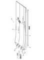
- FIG. 5is an external view schematically showing the external appearance of the display device according to the second embodiment of the present invention.
- the bendable display device 1apixels are arranged in a matrix on a bendable display screen 2.
- Each source drive circuit 6is connected to a source signal and gate drive signal output circuit 8a that outputs a pixel data signal and outputs a shift register drive signal.
- the source signal and gate drive signal output circuit 8ais obtained by integrating the source signal circuit 8 and the gate drive signal output circuit 9 shown in FIG. 1 into one package.
- the source drive circuit 6a closest to the shift register 4is supplied with the shift register drive signal in addition to the pixel data signal from the source signal and gate drive signal output circuit 8a.
- a pixel data signalis supplied to the source drive circuit 6 from the source signal and gate drive signal output circuit 8a.
- the gate drive signal output circuit 9can be reduced, and it is possible to reduce defects due to the reduction in the number of members and the parts cost.
- Other configurations, operations, and functionsare the same as the configurations, operations, and functions described in the first embodiment, and thus description thereof is omitted.
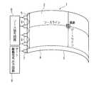
- FIG. 6is an external view schematically showing the external appearance of the display device according to the third embodiment of the present invention.
- the bendable display device 1bis configured such that the bendable display screen 2 is a part of a side surface of a cylinder.
- the edge portions 5 on which the source drive circuits 6 and the input terminals 7 of the shift register 4 are mountedcoincide with the height direction of the cylinder.
- the edge part 5becomes flat in the height direction of a cylinder, and the effect of Example 1 mentioned above can be acquired easily to the maximum.
- the cross section of the cylinderdoes not have to be a perfect circle, but may be an ellipse or a cross section of a column whose curvature changes in the circumferential direction.
- Other configurations, operations, and functionsare the same as the configurations, operations, and functions described in the first and second embodiments, and thus description thereof is omitted.
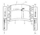
- FIG. 7is an external view schematically showing the external appearance of Embodiment 4 of the display device according to the present invention.
- a plurality of source drive circuits 6are provided on the edge 5
- a source signal circuit 8is connected to each source drive circuit 6
- the edge 10 facing the edge 5is provided on the edge 10.
- a plurality of source drive circuits 6bare provided, and a source signal circuit 8b is connected to each source drive circuit 6b.
- Each source driving circuit 6blike each source driving circuit 6, periodically shares the pixel data signal supplied from the source signal circuit 8b and applies it to each source line.
- the edge portion 10is assumed to have a small curvature similarly to the edge portion 5.
- the input terminal 7 of the shift register 4is provided on the edge 5, and the gate drive signal output circuit 9 is connected to the input terminal 7, and the other edge of the shift register 4 is connected to the edge 10 facing the edge 5.
- An input terminal 7ais provided, and a gate drive signal output circuit 9a is connected to the input terminal 7a.
- the gate drive signal output circuit 9aoutputs a shift register drive signal.
- the source driving circuit 6, the source signal circuit 8, the source driving circuit 6b, the source signal circuit 8b, the input terminal 7, the gate driving signal output circuit 9, the input terminal 7a, and the gate driving signal output circuit 9aare described in the above embodiments. As shown in FIG. 2, merger and omission may be performed as appropriate.
- the drive area per source drive circuit 6 and source drive circuit 6bis halved, so that the display screen 2 can be increased in size and definition.
- the signalis input from both sides to the same source line, even if a source line cut such as a crack due to a curve occurs, the signal is input from both sides of the cut portion, so it does not become a line defect and is displayed. The reliability can be improved.
- Other configurations, operations, and functionsare the same as the configurations, operations, and functions described in the first to third embodiments, and thus description thereof is omitted.
- FIG. 8is an external view schematically showing the external appearance of Embodiment 5 of the display device according to the present invention.
- a shift register 4is provided on the edge 3, and an input terminal 7 of the shift register 4 is provided on the edge 5, and an edge (opposite edge) facing the edge 3 is provided.
- 3ais provided with a shift register 4a, and an input terminal 7b of the shift register 4a is provided on the edge portion 5.
- a gate drive signal output circuit 9bthat outputs a shift register drive signal is connected to the input terminal 7 and the input terminal 7b.
- the edge part 3ashall have a large curvature similarly to the edge part 3.
- the drive area per shift register 4 and shift register 4ais halved, so that the display screen 2 can be increased in size and definition. Also, when a signal is input from both sides to the same gate line, even if a gate line cut such as a crack due to bending occurs, the signal is input from both sides of the cut portion, so it does not become a line defect and is displayed. The reliability can be improved.
- the shift register 4 and the shift register 4amay not be input to the same gate line, and the gate line in the display screen 2 may be shared by the shift register 4 and the shift register 4a. In this case, the effect of avoiding the line defect at the time of cutting the gate line as described above cannot be obtained. However, since the load for each of the shift register 4 and the shift register 4a is reduced, the display screen 2 is increased in size and height. Refinement can be achieved. Other configurations, operations, and functions are the same as the configurations, operations, and functions described in the first to fourth embodiments, and thus description thereof is omitted.
- FIG. 9is an external view schematically showing the external appearance of Embodiment 6 of the display device according to the present invention.
- This bendable display device 1eis shown in a state where the display devices 1 and 1a to 1d of the first to fifth embodiments described above are expanded in a flat shape without being bent.
- the display device 1ehas a bendable portion of the display screen 2 as compared with the vicinity of the edge portions (sides) 5, 5a, 10 on which the source drive circuits 6, 6c and the input terminals 7, 7a are mounted.
- the substrateis formed thin.
- the present inventioncan be used for a display device (flexible display) whose display screen can be bent by a liquid crystal display device, an organic EL display device, an electroconductive display device, or the like.
Landscapes
- Physics & Mathematics (AREA)
- Nonlinear Science (AREA)
- General Physics & Mathematics (AREA)
- Optics & Photonics (AREA)
- Mathematical Physics (AREA)
- Chemical & Material Sciences (AREA)
- Crystallography & Structural Chemistry (AREA)
- Engineering & Computer Science (AREA)
- Theoretical Computer Science (AREA)
- Devices For Indicating Variable Information By Combining Individual Elements (AREA)
- Electroluminescent Light Sources (AREA)
Abstract
Description
Translated fromJapanese本発明は、湾曲可能な表示画面に画素毎のトランジスタがマトリクス状に配置されており、一方向の線上のトランジスタ群毎に、各ゲートを同時に第1周期で順次オンにし、他方向の線上のトランジスタ群毎に、各ソースに同時に第1周期より短い第2周期で画素データ信号を順次与える表示装置に関するものである。In the present invention, transistors for each pixel are arranged in a matrix on a bendable display screen, and for each transistor group on a line in one direction, the gates are sequentially turned on in the first period and on the line in the other direction. The present invention relates to a display device that sequentially supplies pixel data to each source in a second period shorter than the first period for each transistor group.
近時、液晶表示装置、有機EL表示装置及び電気泳導表示装置等で表示画面が湾曲可能な表示装置(フレキシブルディスプレイ)が普及し始めている。
例えば、アクティブマトリクス型の湾曲可能な液晶表示装置では、液晶層を挟持する2枚の湾曲可能な透明基板からなる液晶パネルを備えており、2枚の透明基板のうち一方の透明基板には、多数のゲート(バス)ライン(走査信号線)と多数のソース(バス)ライン(映像信号線)とが格子状に配置されている。
それら多数のゲートライン(例えばマトリクスの行方向)と多数のソースライン(例えばマトリクスの列方向)との各交差点には、それぞれ対応してマトリクス状に配置された画素部が設けられている。Recently, a display device (flexible display) whose display screen can be curved, such as a liquid crystal display device, an organic EL display device, and an electroconductive display device, has begun to spread.
For example, an active matrix type bendable liquid crystal display device includes a liquid crystal panel composed of two bendable transparent substrates that sandwich a liquid crystal layer, and one of the two transparent substrates includes: A large number of gate (bus) lines (scanning signal lines) and a large number of source (bus) lines (video signal lines) are arranged in a grid pattern.
Pixel portions arranged in a matrix are provided at intersections between the large number of gate lines (for example, the row direction of the matrix) and the large number of source lines (for example, the column direction of the matrix).
各画素部は、対応する交差点を通過するゲートラインにゲート端子が接続されると共に、当該交差点を通過するソースラインにソース端子が接続された薄膜トランジスタ(TFT)、及び画素値を保持するための画素容量などを含んでいる。また、上記2枚の透明基板のうち他方の透明基板には、上記の画素部に共通的に設けられた対向電極である共通電極が設けられている。Each pixel portion includes a thin film transistor (TFT) having a gate terminal connected to a gate line passing through a corresponding intersection and a source terminal connected to a source line passing through the intersection, and a pixel for holding a pixel value Includes capacity. The other transparent substrate of the two transparent substrates is provided with a common electrode which is a counter electrode provided in common in the pixel portion.
アクティブマトリクス型の湾曲可能な液晶表示装置は、さらに、上記多数のゲートラインに接続され、同じゲートラインに接続された各ゲートを同時に、ゲートライン毎には周期的に順次オンにして行くゲート駆動回路と、ゲート駆動回路を駆動する為の駆動信号を出力するゲート駆動信号出力回路と、上記多数のソースラインに接続され、同じソースラインに接続された各ソースに同時に、ソースライン毎には周期的に順次画素データ信号を与えて行くソース駆動回路及びソース信号回路とを備えている。The active matrix type bendable liquid crystal display device is further connected to the above-mentioned multiple gate lines, and the gate drive is performed such that each gate connected to the same gate line is turned on simultaneously and periodically for each gate line. A circuit, a gate drive signal output circuit that outputs a drive signal for driving the gate drive circuit, and a number of cycles connected to each source connected to the same source line and connected to the same source line. A source driving circuit and a source signal circuit for sequentially supplying pixel data signals.
画素データを示す映像信号はソースラインによって伝達されるが、各ソースラインは複数行分の画素データを示す映像信号を同時には伝達することができない。このため、上述したマトリクス状に配置された画素部内の画素容量への映像信号の書き込みは、1行ずつ順次に行われる。そこで、多数のゲートラインから1本、所定期間ずつ順次に選択されるように、ゲート駆動回路は多数段からなるシフトレジスタによって構成されている。The video signal indicating the pixel data is transmitted by the source line, but each source line cannot transmit the video signal indicating the pixel data for a plurality of rows at the same time. For this reason, the writing of the video signal to the pixel capacitors in the pixel portions arranged in the above-described matrix is sequentially performed row by row. Therefore, the gate driving circuit is constituted by a shift register having a plurality of stages so that one gate line is sequentially selected from a large number of gate lines.
また、液晶表示装置に関し、近年、ゲートドライバのモノリシック化が進んでいる。従来、ゲートドライバは液晶パネルを構成する基板の周辺部にIC(Integrated Circuit)チップとして搭載されることが多かったが、近年、基板上に直接的にゲートドライバを形成することが多くなされるようになっている。このようなゲートドライバは「モノリシックゲートドライバ」などと呼ばれている。また、モノリシックゲートドライバを備えたパネルは「ゲートドライバモノリシックパネル」などと呼ばれている。Also, with regard to liquid crystal display devices, in recent years, gate drivers have become monolithic. Conventionally, the gate driver is often mounted as an IC (Integrated Circuit) chip on the periphery of the substrate constituting the liquid crystal panel, but in recent years, the gate driver is often formed directly on the substrate. It has become. Such a gate driver is called a “monolithic gate driver”. A panel having a monolithic gate driver is called a “gate driver monolithic panel”.
特許文献1には、可撓性を有する基板上に、表示部と、外部から信号が入力され得る複数の接続端子と、複数の配線とを有し、接続端子の一は、配線の一によって表示部と電気的に接続された表示装置が開示されている。配線は、複数本に分岐した第1の部分と、複数本が1本に収束した第2の部分とを有し、外部からの信号を1つに纏めて入力する。
この表示装置は、外部からの信号を1か所から全体へ引回す必要があり、大型化、及び信号数が増える高精細化には不向きである。
This display device needs to route an external signal from one place to the whole, and is not suitable for increasing the size and increasing the number of signals.
上述したような湾曲可能な表示装置では、湾曲可能な例えばマトリクスの行方向の縁辺部に実装されたソース駆動回路が剥がれる等の実装不良が発生し、生産歩留まり及び信頼性が低下するという問題がある。In the bendable display device as described above, there is a problem in that the production yield and reliability are lowered due to a mounting failure such as peeling of the source driving circuit mounted on the edge in the row direction of the matrix. is there.
本発明は、このような事情に鑑みてなされたものであり、ソース駆動回路が剥がれる等の実装不良が発生し難く、生産歩留まり及び信頼性が低下しない湾曲可能な表示装置を提供することを目的とする。The present invention has been made in view of such circumstances, and it is an object of the present invention to provide a bendable display device in which mounting defects such as peeling of a source drive circuit are unlikely to occur, and production yield and reliability are not reduced. And
本発明に係る表示装置は、湾曲可能な表示画面に画素毎のトランジスタがマトリクス状に配置されており、一方向の線上の前記トランジスタ群毎に、各ゲートを同時に順次オンにするゲート駆動回路と、他方向の線上の前記トランジスタ群毎に、各ソースに同時に画素データ信号を順次与えて行く為の複数のソース駆動回路とを備える表示装置において、前記ソース駆動回路は、前記表示画面の、第1曲率で湾曲可能な辺に設けられ、前記ゲート駆動回路は、前記表示画面の、前記第1曲率より大きい第2曲率で湾曲可能な他辺に設けられていることを特徴とする。A display device according to the present invention includes a gate driving circuit in which transistors for each pixel are arranged in a matrix on a bendable display screen, and each gate is sequentially turned on for each of the transistor groups on a line in one direction. A display device comprising a plurality of source driving circuits for sequentially supplying a pixel data signal to each source at the same time for each of the transistor groups on the line in the other direction, The gate drive circuit is provided on a side that can be bent with a second curvature larger than the first curvature of the display screen.
本発明に係る表示装置は、前記一方向の線上の前記トランジスタ群毎に、各ゲートを同時に順次オンにして行く為の駆動信号を、前記ゲート駆動回路へ出力するゲート駆動信号出力回路と、前記ソース駆動回路に前記画素データ信号を与えるソース信号回路とを更に備え、前記ゲート駆動信号出力回路及びソース信号回路は、前記第1曲率で湾曲可能な辺近傍に設けられていることを特徴とする。The display device according to the present invention includes a gate drive signal output circuit that outputs, to the gate drive circuit, a drive signal for sequentially turning on each gate for each of the transistor groups on the unidirectional line, A source signal circuit for supplying the pixel data signal to the source drive circuit, wherein the gate drive signal output circuit and the source signal circuit are provided in the vicinity of a side that can be bent with the first curvature. .
本発明に係る表示装置は、前記ゲート駆動回路は、ビット毎に記憶した各データを前記各ゲートに出力するシフトレジスタであり、前記ゲート駆動信号出力回路は、該シフトレジスタを駆動する信号を出力することを特徴とする。In the display device according to the present invention, the gate driving circuit is a shift register that outputs each data stored for each bit to each gate, and the gate driving signal output circuit outputs a signal for driving the shift register. It is characterized by doing.
本発明に係る表示装置は、前記ソース信号回路及びゲート駆動信号出力回路は、ソース信号及びゲート駆動信号出力回路に集約されており、該ソース信号及びゲート駆動信号出力回路が出力したゲート駆動信号は、前記ソース駆動回路経由で前記ゲート駆動回路に与えられるように構成されていることを特徴とする。In the display device according to the present invention, the source signal circuit and the gate drive signal output circuit are integrated into the source signal and the gate drive signal output circuit, and the gate drive signal output from the source signal and the gate drive signal output circuit is The gate driving circuit is configured to be supplied to the gate driving circuit via the source driving circuit.
本発明に係る表示装置は、前記表示画面は、柱体の側面の一部となるように形成されており、前記第1曲率で湾曲可能な辺は、前記表示画面の、前記柱体の高さ方向の辺であり、前記第2曲率で湾曲可能な他辺は、前記表示画面の、前記柱体の周方向の他辺であることを特徴とする。In the display device according to the present invention, the display screen is formed to be a part of a side surface of a column, and the side that can be bent with the first curvature is a height of the column of the display screen. The other side which is a side in the vertical direction and can be bent with the second curvature is the other side of the display screen in the circumferential direction of the column body.
本発明に係る表示装置は、前記ソース駆動回路は、前記第1曲率で湾曲可能な辺、及び該辺に対向する辺に設けられ、前記ゲート駆動信号出力回路及びソース信号回路は、前記第1曲率で湾曲可能な辺、及び該辺に対向する辺近傍に設けられていることを特徴とする。In the display device according to the present invention, the source driving circuit is provided on a side that can be bent with the first curvature, and a side that faces the side, and the gate driving signal output circuit and the source signal circuit are provided on the first side. It is characterized in that it is provided in the vicinity of a side that can be bent with a curvature and that faces the side.
本発明に係る表示装置は、前記ゲート駆動回路は、前記第2曲率で湾曲可能な他辺、及び該他辺に対向する他辺に設けられ、前記他辺、及び該他辺に対向する他辺に設けられた各ゲート駆動回路は、前記ゲート駆動信号出力回路が出力した駆動信号を与えられるように構成してあることを特徴とする。In the display device according to the aspect of the invention, the gate driving circuit may be provided on the other side that can be bent with the second curvature and the other side that faces the other side, and the other side and the other side that faces the other side. Each gate drive circuit provided on the side is configured to be supplied with the drive signal output from the gate drive signal output circuit.
本発明に係る表示装置は、前記表示画面の前記第2曲率で湾曲可能な部分は、前記表示画面の前記第1曲率で湾曲可能な部分より薄く形成されていることを特徴とする。The display device according to the present invention is characterized in that a portion of the display screen that can be bent with the second curvature is formed thinner than a portion of the display screen that can be bent with the first curvature.
本発明に係る表示装置によれば、ソース駆動回路が剥がれる等の実装不良が発生し難く、生産歩留まり及び信頼性が低下しない湾曲可能な表示装置を実現することができる。According to the display device of the present invention, it is possible to realize a bendable display device in which mounting defects such as peeling of the source drive circuit are unlikely to occur, and production yield and reliability are not reduced.
以下に、本発明をその実施例を示す図面に基づいて説明する。Hereinafter, the present invention will be described with reference to the drawings illustrating the embodiments.
図1は、本発明に係る表示装置の実施例1の外観を模式的に示す外観図である。
この湾曲可能な表示装置1は、湾曲可能な表示画面2に画素がマトリクス状に配置されており、画素毎に薄膜トランジスタ(TFT)23(図3)が設けられている。
表示画面2の、曲率がより大きく湾曲可能な(湾曲し易い)マトリクス状の行方向の一方の縁辺部(他辺)3には、シフトレジスタ4が設けられている。シフトレジスタ4は、マトリクス状の列方向の線(ゲートライン)上の薄膜トランジスタ23(図3)群毎に、各ゲートを同時に第1周期で順次オンにして行くゲート駆動回路である。FIG. 1 is an external view schematically showing an external appearance of a display device according to a first embodiment of the present invention.
In the
A
表示画面2の、曲率がより小さく湾曲可能なマトリクス状の列方向の一方の縁辺部(辺)5には、複数のソース駆動回路6が設けられている。ソース駆動回路6は、マトリクス状の行方向の線(ソースライン)上の薄膜トランジスタ23(図3)群毎に、各ソースに同時に第1周期より短い第2周期で画素データ信号を順次供給して行く。
各ソース駆動回路6には、画素データ信号を出力するソース信号回路8が接続されており、各ソース駆動回路6は、ソース信号回路8から供給された画素データ信号を、周期的に分担して各ソースラインに供給して行く。A plurality of
Each
シフトレジスタ4の入力端子7は、縁辺部5及び縁辺部3の交差部に設けられている。入力端子7には、ゲートライン上の薄膜トランジスタ23(図3)群毎に、各ゲートを同時に第1周期で順次オンにして行く為のシフトレジスタ駆動信号を出力するゲート駆動信号出力回路9が接続されている。
尚、ソース信号回路8及びゲート駆動信号出力回路9は、曲率が大きい湾曲可能な表示画面2ではなく、縁辺部5近傍の曲率がより小さい湾曲可能な基板上に形成されている。The
The
また、ソース駆動回路6、シフトレジスタ4及び入力端子7は、表示画面2とは別の基板上に形成されている(モノリシック化されていない)場合も含むものとする。
また、図1では、表示画面2が凸になるようになるように湾曲しているが、表示画面2が凸になる場合に限らず、凹になる場合、更に凹凸に自在に湾曲する場合も含むものとする。また、図1では、表示画面2を方形に表現しているが、方形に限定されるものではない。In addition, the
In FIG. 1, the
図2は、本発明に係る表示装置1が液晶表示装置である場合の、液晶パネルの断面を厚さ方向に拡大して模式的に示す断面図である。
この液晶パネルは、湾曲可能な透明な2枚の基板12,18が、液晶層15を挟み込む構成であり、基板12,18間の液晶層15内には、複数のスペーサ22が設けられている。
基板12の液晶層15側表面には、透明電極13が形成され、透明電極13が液晶層15に接する面には、配向膜14が形成されている。FIG. 2 is a cross-sectional view schematically showing an enlarged cross section of the liquid crystal panel in the thickness direction when the
In this liquid crystal panel, two
A
基板18の液晶層15側表面には、画素電極17が形成され、画素電極17が液晶層15に接する面には、配向膜16が形成されている。
基板12,18の各外側には、偏光板11,19がそれぞれ設けられており、偏光板19の外側には、湾曲可能な導光板20と、導光板20の光源であるLED(発光ダイオード)21とが設けられている。A
Polarizing
図3は、図2に示す液晶パネルの各画素に設けられた画素部の等価回路の例を示す回路図である。
この液晶パネルはアクティブマトリクス型であり、マトリクス状に配置された画素毎の薄膜トランジスタ23と、マトリクスの行方向に配線され、行毎の各薄膜トランジスタ23の各ソースに接続された各ソースライン28と、マトリクスの列方向に配線され、列毎の各薄膜トランジスタ23の各ゲートに接続された各ゲートライン27とを備えている。FIG. 3 is a circuit diagram showing an example of an equivalent circuit of a pixel portion provided in each pixel of the liquid crystal panel shown in FIG.
This liquid crystal panel is of an active matrix type, the
各薄膜トランジスタ23のドレインには、画素電極17(図2)が接続され、画素電極17は、対向する透明電極13(図2)との間に画素容量24を、共通電極26との間に補助容量25を形成している。尚、図3においては、太線で示した部分に電圧が印加されている。A pixel electrode 17 (FIG. 2) is connected to the drain of each
このような構成の画素部では、ゲートライン27に印加された電圧により、そのゲートライン27に接続された1列分全ての薄膜トランジスタ23がオンになることで、ソース及びドレイン間に電流が流れる。その際、ソースライン28に印加されている各画素データ信号が画素容量24に印加され、当該画素容量24に対応する液晶層15は、印加された画素信号データ信号に応じた表示光を透過させ、コンデンサ25には、画素データ信号に応じた電荷が蓄積される。In the pixel portion having such a configuration, a current applied between the source and the drain flows when all of the
ゲートライン27の1列分の画素容量24及び補助容量25への充電を終えると、電圧の印加は次のゲートライン27へ移り、前の1列分の薄膜トランジスタ23は、ゲートにロー(low)レベルの電圧が印加されてオフになる。前の1列分の画素容量24は、ソースライン28からの画素データ信号が印加されなくなるが、同時に補助容量25に蓄積された電荷により、次に当該ゲートライン27が選択される迄の1フレームの時間分、必要な電圧を略維持できる。When the charging of the
図4は、本発明に係る表示装置1が有機EL(Electro Luminescence)表示装置である場合の、有機ELパネルの断面を厚さ方向に拡大して模式的に示す断面図である。
この有機ELパネルでは、湾曲可能な透明な基板36上に、有機半導体層、並びに有機半導体層を挟み込む画素毎の陽極35、及び陰極31が積層されている。有機半導体層は、発光層33、並びに発光層33を挟み込むホール輸送層34及び電子輸送層32が積層されている。
基板36及び陽極35間には、有機半導体層を劣化させる水及び酸素分子の侵入を防止する為のガスバリア膜37が形成され、陰極31の外側にも、水及び酸素分子が有機半導体層へ侵入するのを防止する為の封止膜30が形成されている。FIG. 4 is a cross-sectional view schematically showing an enlarged cross section of the organic EL panel in the thickness direction when the
In this organic EL panel, an organic semiconductor layer, and an
A
このような構成の有機ELパネルでは、陰極31及び陽極35からそれぞれ注入される電子及びホールが、当該陰極31及び陽極35に対応する有機半導体層の電子輸送層32及びホール輸送層34を通過して、発光層33で再結合する為、光が放出される。
印加された画素データ信号に応じて、陰極31及び陽極35からそれぞれ注入される電子及びホールは増減し、発光層33から放出される光量も増減する。尚、陰極31及び陽極35間に印加される画素データ信号は、図3に示す画素部に類似した画素部により与えられる。In the organic EL panel having such a configuration, electrons and holes injected from the
In accordance with the applied pixel data signal, the number of electrons and holes injected from the
このような表示装置1では、表示画面2の、湾曲し易い縁辺部3に、薄膜トランジスタ23の各ゲートを第1周期で順次オンにして行くシフトレジスタ4が設けられている。また、湾曲し難い縁辺部5には、薄膜トランジスタ23の各ソースに第1周期より短い第2周期で画素データ信号を順次与えて行く為の複数のソース駆動回路6が設けられている。In such a
これにより、回路構成が簡単でより湾曲し易いように形成できるシフトレジスタ4を、湾曲し易い縁辺部3に設けることができ、回路構成が複雑で湾曲し易いように形成するのが難しいソース駆動回路6を、湾曲し難い縁辺部5に設けることができるので、ソース駆動回路が剥がれる等の実装不良を発生し難くすることができる。
また、ソース駆動回路6の実装部の曲率を最小にすることができ、曲率を吸収する為のCOF(Chip On Film)の冗長性、及びソース駆動回路6の湾曲化が不要となる他、湾曲し易い縁辺部3に、ゲート駆動信号出力回路9を実装する必要が無く、より湾曲し易い表示装置を実現することが可能となる。As a result, the
In addition, the curvature of the mounting portion of the
図5は、本発明に係る表示装置の実施例2の外観を模式的に示す外観図である。
この湾曲可能な表示装置1aは、湾曲可能な表示画面2に画素がマトリクス状に配置されている。
各ソース駆動回路6には、画素データ信号を出力し、シフトレジスタ駆動信号を出力するソース信号及びゲート駆動信号出力回路8aが接続されている。ソース信号及びゲート駆動信号出力回路8aは、図1に示すソース信号回路8及びゲート駆動信号出力回路9が1つのパッケージに集約されたものである。FIG. 5 is an external view schematically showing the external appearance of the display device according to the second embodiment of the present invention.
In the bendable display device 1a, pixels are arranged in a matrix on a
Each
ソース駆動回路6の内、シフトレジスタ4に最も近いソース駆動回路6aには、ソース信号及びゲート駆動信号出力回路8aから、画素データ信号の他、シフトレジスタ駆動信号が供給される。ソース駆動回路6には、ソース信号及びゲート駆動信号出力回路8aから、画素データ信号が供給される。
これにより、ゲート駆動信号出力回路9を削減でき、部材点数削減による不具合低減、及び部品コストの低減を図ることができる。その他の構成、動作及び作用は、実施例1で説明した構成、動作及び作用と同様であるので、説明を省略する。Of the
Thereby, the gate drive
図6は、本発明に係る表示装置の実施例3の外観を模式的に示す外観図である。
この湾曲可能な表示装置1bは、湾曲可能な表示画面2が,円柱の側面の一部となるように構成されている。
各ソース駆動回路6、及びシフトレジスタ4の入力端子7が実装される縁辺部5は、円柱の高さ方向に一致している。FIG. 6 is an external view schematically showing the external appearance of the display device according to the third embodiment of the present invention.
The
The
これにより、縁辺部5は円柱の高さ方向に平坦となり、上述した実施例1の効果を簡単に最大限に得ることができる。
尚、ここでの円柱の断面は真円である必要はなく、楕円、又は周方向で曲率が変化するような柱体の断面であっても良い。その他の構成、動作及び作用は、実施例1,2で説明した構成、動作及び作用と同様であるので、説明を省略する。Thereby, the
Here, the cross section of the cylinder does not have to be a perfect circle, but may be an ellipse or a cross section of a column whose curvature changes in the circumferential direction. Other configurations, operations, and functions are the same as the configurations, operations, and functions described in the first and second embodiments, and thus description thereof is omitted.
図7は、本発明に係る表示装置の実施例4の外観を模式的に示す外観図である。
この湾曲可能な表示装置1cは、縁辺部5に複数のソース駆動回路6が設けられ、各ソース駆動回路6にソース信号回路8が接続されている他、縁辺部5に対向する縁辺部10に複数のソース駆動回路6bが設けられ、各ソース駆動回路6bにソース信号回路8bが接続されている。各ソース駆動回路6bは、各ソース駆動回路6と同様に、ソース信号回路8bから与えられた画素データ信号を、周期的に分担して各ソースラインに与えて行く。尚、縁辺部10は、縁辺部5と同様に、曲率は小さいものとする。FIG. 7 is an external view schematically showing the external appearance of
In the
シフトレジスタ4の入力端子7が、縁辺部5に設けられ、入力端子7にゲート駆動信号出力回路9が接続されている他、縁辺部5に対向する縁辺部10に、シフトレジスタ4の他の入力端子7aが設けられ、入力端子7aにゲート駆動信号出力回路9aが接続されている。ゲート駆動信号出力回路9aは、ゲート駆動信号出力回路9と同様に、シフトレジスタ駆動信号を出力する。尚、ソース駆動回路6、ソース信号回路8、ソース駆動回路6b、ソース信号回路8b、入力端子7、ゲート駆動信号出力回路9、入力端子7a及びゲート駆動信号出力回路9aについては、上述した実施例2のように、適宜、併合及び省略をしても良い。The
これにより、ソース駆動回路6及びソース駆動回路6b当たりの駆動面積が半減する為、表示画面2の大型化及び高精細化を図ることができる。また、同一ソースラインに両側から信号を入力する場合に、湾曲によるクラック等のソースライン切断が発生したときでも、切断部の両側から信号が入力されている為、線欠陥とはならず、表示を維持することができて、信頼性が向上する。その他の構成、動作及び作用は、実施例1~3で説明した構成、動作及び作用と同様であるので、説明を省略する。Thereby, the drive area per
図8は、本発明に係る表示装置の実施例5の外観を模式的に示す外観図である。
この湾曲可能な表示装置1dは、縁辺部3にシフトレジスタ4が設けられ,シフトレジスタ4の入力端子7が、縁辺部5に設けられている他、縁辺部3に対向する縁辺部(他辺)3aにシフトレジスタ4aが設けられ,シフトレジスタ4aの入力端子7bが、縁辺部5に設けられている。入力端子7及び入力端子7bには、シフトレジスタ駆動信号を出力するゲート駆動信号出力回路9bが接続されている。尚、縁辺部3aは、縁辺部3と同様に、曲率は大きいものとする。FIG. 8 is an external view schematically showing the external appearance of
In this
これにより、シフトレジスタ4及びシフトレジスタ4a当たりの駆動面積が半減する為、表示画面2の大型化及び高精細化を図ることができる。また、同一ゲートラインに両側から信号を入力する場合に、湾曲によるクラック等のゲートライン切断が発生したときでも、切断部の両側から信号が入力されている為、線欠陥とはならず、表示を維持することができて、信頼性が向上する。As a result, the drive area per
尚、シフトレジスタ4及びシフトレジスタ4aを同一ゲートラインに入力させず、表示画面2内のゲートラインをシフトレジスタ4及びシフトレジスタ4aで分担させるように構成することも可能である。この場合、上述したようなゲートライン切断時の線欠陥を回避できるような効果は得られないが、シフトレジスタ4及びシフトレジスタ4a毎の負荷が削減される為、表示画面2の大型化及び高精細化を図ることができる。その他の構成、動作及び作用は、実施例1~4で説明した構成、動作及び作用と同様であるので、説明を省略する。The
図9は、本発明に係る表示装置の実施例6の外観を模式的に示す外観図である。
この湾曲可能な表示装置1eは、上述した実施例1~5の表示装置1,1a~1dを湾曲させずに平面状に展開した状態で示してある。
この表示装置1eは、表示画面2の、ソース駆動回路6,6c及び入力端子7,7aが実装される縁辺部(辺)5,5a,10付近に比較して、表示画面2の湾曲可能部分の基板は薄く形成されている。FIG. 9 is an external view schematically showing the external appearance of
This bendable display device 1e is shown in a state where the
The display device 1e has a bendable portion of the
本実施例6では、実施例1~5において、曲率が小さい縁辺部5,5a,10付近を除く湾曲させる部分のみを薄型化しており、ソース駆動回路6,6c及び入力端子7,7a等を曲率が小さい縁辺部5,5a,10に実装し、シフトレジスタ4,4aを曲率が大きい縁辺部3,3aに実装している。
これにより、生産歩留まりを低下させることなく、より曲率が大きい湾曲可能な表示装置を実現することができる。その他の構成、動作及び作用は、実施例1~5で説明した構成、動作及び作用と同様であるので、説明を省略する。In the sixth embodiment, in the first to fifth embodiments, only the portions to be bent except for the vicinity of the
As a result, it is possible to realize a bendable display device having a larger curvature without reducing the production yield. Other configurations, operations, and functions are the same as the configurations, operations, and functions described in the first to fifth embodiments, and thus description thereof is omitted.
本実施例1~6は、全ての点で例示であって制限的なものではないと考えるべきである。本発明の範囲は上述の説明ではなく請求の範囲によって示され、請求の範囲と均等の意味及び範囲内での全ての変更が含まれることが意図される。The Examples 1 to 6 should be considered as illustrative in all points and not restrictive. The scope of the present invention is defined by the terms of the claims, rather than the description above, and is intended to include any modifications within the scope and meaning equivalent to the terms of the claims.
本発明は、液晶表示装置、有機EL表示装置及び電気泳導表示装置等で表示画面が湾曲可能な表示装置(フレキシブルディスプレイ)に利用することができる。The present invention can be used for a display device (flexible display) whose display screen can be bent by a liquid crystal display device, an organic EL display device, an electroconductive display device, or the like.
1,1a~1e 表示装置
2 表示画面
3,3a 縁辺部(他辺)
4,4a シフトレジスタ(ゲート駆動回路)
5,5a,10 縁辺部(辺)
6,6a~6c ソース駆動回路
7,7a,7b 入力端子
8,8b ソース信号回路
8a ソース信号及びゲート駆動信号出力回路
9,9a,9b ゲート駆動信号出力回路
23 薄膜トランジスタ
27 ゲートライン
28 ソースライン1, 1a to
4,4a Shift register (gate drive circuit)
5, 5a, 10 Edge (side)
6, 6a to 6c
Claims (8)
Translated fromJapanese一方向の線上の前記トランジスタ群毎に、各ゲートを同時に順次オンにするゲート駆動回路と、
他方向の線上の前記トランジスタ群毎に、各ソースに同時に画素データ信号を順次与えて行く為の複数のソース駆動回路と
を備える表示装置において、
前記ソース駆動回路は、前記表示画面の、第1曲率で湾曲可能な辺に設けられ、前記ゲート駆動回路は、前記表示画面の、前記第1曲率より大きい第2曲率で湾曲可能な他辺に設けられていることを特徴とする表示装置。Transistors for each pixel are arranged in a matrix on a bendable display screen,
A gate driving circuit for sequentially turning on each gate at the same time for each transistor group on a unidirectional line;
In a display device comprising a plurality of source driving circuits for sequentially supplying pixel data signals to the respective sources simultaneously for each of the transistor groups on the line in the other direction,
The source driving circuit is provided on a side of the display screen that can be bent with a first curvature, and the gate driving circuit is provided on the other side of the display screen that can be bent with a second curvature larger than the first curvature. A display device characterized by being provided.
前記ソース駆動回路に前記画素データ信号を与えるソース信号回路と
を更に備え、
前記ゲート駆動信号出力回路及びソース信号回路は、前記第1曲率で湾曲可能な辺近傍に設けられている請求項1に記載の表示装置。A gate drive signal output circuit for outputting a drive signal for sequentially turning on each gate to each of the transistor groups on the unidirectional line to the gate drive circuit;
A source signal circuit for supplying the pixel data signal to the source driving circuit,
The display device according to claim 1, wherein the gate drive signal output circuit and the source signal circuit are provided in the vicinity of a side that can be bent with the first curvature.
前記ゲート駆動信号出力回路は、該シフトレジスタを駆動する信号を出力する請求項2に記載の表示装置。The gate drive circuit is a shift register that outputs each data stored for each bit to each gate,
The display device according to claim 2, wherein the gate drive signal output circuit outputs a signal for driving the shift register.
前記第1曲率で湾曲可能な辺は、前記表示画面の、前記柱体の高さ方向の辺であり、前記第2曲率で湾曲可能な他辺は、前記表示画面の、前記柱体の周方向の他辺である請求項1乃至4の何れか1項に記載の表示装置。The display screen is formed to be a part of the side surface of the column body,
The side that can be bent with the first curvature is a side of the display screen in the height direction of the column, and the other side that can be bent with the second curvature is the circumference of the column of the display screen. The display device according to claim 1, wherein the display device is the other side of the direction.
Priority Applications (2)
| Application Number | Priority Date | Filing Date | Title |
|---|---|---|---|
| PCT/JP2015/069447WO2017006419A1 (en) | 2015-07-06 | 2015-07-06 | Display device |
| US15/862,532US10338424B2 (en) | 2015-07-06 | 2018-01-04 | Curved display apparatus |
Applications Claiming Priority (1)
| Application Number | Priority Date | Filing Date | Title |
|---|---|---|---|
| PCT/JP2015/069447WO2017006419A1 (en) | 2015-07-06 | 2015-07-06 | Display device |
Related Child Applications (1)
| Application Number | Title | Priority Date | Filing Date |
|---|---|---|---|
| US15/862,532Continuation-In-PartUS10338424B2 (en) | 2015-07-06 | 2018-01-04 | Curved display apparatus |
Publications (1)
| Publication Number | Publication Date |
|---|---|
| WO2017006419A1true WO2017006419A1 (en) | 2017-01-12 |
Family
ID=57685523
Family Applications (1)
| Application Number | Title | Priority Date | Filing Date |
|---|---|---|---|
| PCT/JP2015/069447CeasedWO2017006419A1 (en) | 2015-07-06 | 2015-07-06 | Display device |
Country Status (2)
| Country | Link |
|---|---|
| US (1) | US10338424B2 (en) |
| WO (1) | WO2017006419A1 (en) |
Cited By (4)
| Publication number | Priority date | Publication date | Assignee | Title |
|---|---|---|---|---|
| CN106952607A (en)* | 2017-05-25 | 2017-07-14 | 京东方科技集团股份有限公司 | Display substrate, display panel and display device |
| CN111312076A (en)* | 2020-03-03 | 2020-06-19 | 武汉华星光电半导体显示技术有限公司 | Flexible display panel and display device |
| WO2021249195A1 (en)* | 2020-06-12 | 2021-12-16 | 中兴通讯股份有限公司 | Flexible screen support device and intelligent terminal |
| CN115311983A (en)* | 2022-09-06 | 2022-11-08 | 武汉天马微电子有限公司 | Display panel and display device |
Families Citing this family (2)
| Publication number | Priority date | Publication date | Assignee | Title |
|---|---|---|---|---|
| CN108873444B (en)* | 2018-07-17 | 2021-11-09 | Tcl华星光电技术有限公司 | Flexible light guide plate and flexible display |
| US11087661B2 (en)* | 2019-03-05 | 2021-08-10 | Innolux Corporation | Display device having curved portion |
Citations (10)
| Publication number | Priority date | Publication date | Assignee | Title |
|---|---|---|---|---|
| JPH02247618A (en)* | 1989-03-20 | 1990-10-03 | Toshiba Corp | liquid crystal display device |
| JP2003044004A (en)* | 2001-07-27 | 2003-02-14 | Seiko Epson Corp | Scan line drive circuit, electro-optical device, electronic device, and semiconductor device |
| JP2005284252A (en)* | 2004-03-29 | 2005-10-13 | Samsung Sdi Co Ltd | Flat panel display device |
| JP2005338179A (en)* | 2004-05-24 | 2005-12-08 | Sharp Corp | Display device |
| JP2007123861A (en)* | 2005-09-29 | 2007-05-17 | Semiconductor Energy Lab Co Ltd | Semiconductor device and manufacturing method thereof |
| JP2008020836A (en)* | 2006-07-14 | 2008-01-31 | Nec Lcd Technologies Ltd | Display device and manufacturing method thereof |
| JP2009180904A (en)* | 2008-01-30 | 2009-08-13 | Sharp Corp | Display device and driver IC used therefor |
| JP2010282181A (en)* | 2009-05-02 | 2010-12-16 | Semiconductor Energy Lab Co Ltd | E-book |
| JP2012159633A (en)* | 2011-01-31 | 2012-08-23 | Seiko Epson Corp | Active matrix substrate, electro-optical device and electronic apparatus |
| JP2013134295A (en)* | 2011-12-26 | 2013-07-08 | Panasonic Corp | Curved surface display |
Family Cites Families (6)
| Publication number | Priority date | Publication date | Assignee | Title |
|---|---|---|---|---|
| WO2004049050A1 (en)* | 2002-11-22 | 2004-06-10 | Koninklijke Philips Electronics N.V. | Method of manufacturing a curved display |
| CN101044627B (en)* | 2004-09-15 | 2012-02-08 | 株式会社半导体能源研究所 | Semiconductor device |
| EP1770788A3 (en) | 2005-09-29 | 2011-09-21 | Semiconductor Energy Laboratory Co., Ltd. | Semiconductor device having oxide semiconductor layer and manufacturing method thereof |
| JP5070340B2 (en)* | 2008-08-07 | 2012-11-14 | シャープ株式会社 | Display device |
| JP5640365B2 (en)* | 2009-12-07 | 2014-12-17 | ソニー株式会社 | Display device and display device control method |
| TWI790673B (en) | 2013-03-07 | 2023-01-21 | 日商半導體能源研究所股份有限公司 | Electronic device |
- 2015
- 2015-07-06WOPCT/JP2015/069447patent/WO2017006419A1/ennot_activeCeased
- 2018
- 2018-01-04USUS15/862,532patent/US10338424B2/enactiveActive
Patent Citations (10)
| Publication number | Priority date | Publication date | Assignee | Title |
|---|---|---|---|---|
| JPH02247618A (en)* | 1989-03-20 | 1990-10-03 | Toshiba Corp | liquid crystal display device |
| JP2003044004A (en)* | 2001-07-27 | 2003-02-14 | Seiko Epson Corp | Scan line drive circuit, electro-optical device, electronic device, and semiconductor device |
| JP2005284252A (en)* | 2004-03-29 | 2005-10-13 | Samsung Sdi Co Ltd | Flat panel display device |
| JP2005338179A (en)* | 2004-05-24 | 2005-12-08 | Sharp Corp | Display device |
| JP2007123861A (en)* | 2005-09-29 | 2007-05-17 | Semiconductor Energy Lab Co Ltd | Semiconductor device and manufacturing method thereof |
| JP2008020836A (en)* | 2006-07-14 | 2008-01-31 | Nec Lcd Technologies Ltd | Display device and manufacturing method thereof |
| JP2009180904A (en)* | 2008-01-30 | 2009-08-13 | Sharp Corp | Display device and driver IC used therefor |
| JP2010282181A (en)* | 2009-05-02 | 2010-12-16 | Semiconductor Energy Lab Co Ltd | E-book |
| JP2012159633A (en)* | 2011-01-31 | 2012-08-23 | Seiko Epson Corp | Active matrix substrate, electro-optical device and electronic apparatus |
| JP2013134295A (en)* | 2011-12-26 | 2013-07-08 | Panasonic Corp | Curved surface display |
Cited By (6)
| Publication number | Priority date | Publication date | Assignee | Title |
|---|---|---|---|---|
| CN106952607A (en)* | 2017-05-25 | 2017-07-14 | 京东方科技集团股份有限公司 | Display substrate, display panel and display device |
| CN106952607B (en)* | 2017-05-25 | 2020-04-17 | 京东方科技集团股份有限公司 | Display substrate, display panel and display device |
| CN111312076A (en)* | 2020-03-03 | 2020-06-19 | 武汉华星光电半导体显示技术有限公司 | Flexible display panel and display device |
| WO2021249195A1 (en)* | 2020-06-12 | 2021-12-16 | 中兴通讯股份有限公司 | Flexible screen support device and intelligent terminal |
| US12197252B2 (en) | 2020-06-12 | 2025-01-14 | Zte Corporation | Flexible screen support device and intelligent terminal |
| CN115311983A (en)* | 2022-09-06 | 2022-11-08 | 武汉天马微电子有限公司 | Display panel and display device |
Also Published As
| Publication number | Publication date |
|---|---|
| US20180129096A1 (en) | 2018-05-10 |
| US10338424B2 (en) | 2019-07-02 |
Similar Documents
| Publication | Publication Date | Title |
|---|---|---|
| KR102825735B1 (en) | Array substrate, display panel, bonded display panel and display driving method | |
| US10591753B2 (en) | Electroluminescent display | |
| US10199447B2 (en) | Display device | |
| US10439016B2 (en) | Array substrate and display panel | |
| US20190164999A1 (en) | Thin-Film Transistor Array Substrate and Organic Light-Emitting Display Device Including the Same | |
| KR101484642B1 (en) | Organic light emitting display device | |
| WO2017006419A1 (en) | Display device | |
| US11374067B2 (en) | Display device | |
| US20200091273A1 (en) | Tiling display device | |
| CN107689209B (en) | Display device | |
| CN112840475A (en) | display screen | |
| US8823010B2 (en) | Thin-film transistor array substrate and display device including the same | |
| CN106935170A (en) | Flexible display apparatus | |
| CN113078174A (en) | Array substrate, display panel and display device | |
| KR102502183B1 (en) | Display module | |
| WO2016206224A1 (en) | In-cell touch display panel, driving method therefor, and display device | |
| CN105825811A (en) | Non-rectangular display | |
| CN108123054B (en) | Flexible display | |
| US20190043892A1 (en) | Display device | |
| US10529782B2 (en) | Organic light emitting display device including moisture-transmission delay layer which covers edges of lines | |
| JP2010231931A (en) | Light-emitting device and method of manufacturing the same | |
| KR20250054024A (en) | Display substrates and display devices | |
| JP5110325B2 (en) | Light emitting device and manufacturing method thereof | |
| KR20180062522A (en) | Flexible display device | |
| US12389770B2 (en) | Display panel and display device |
Legal Events
| Date | Code | Title | Description |
|---|---|---|---|
| 121 | Ep: the epo has been informed by wipo that ep was designated in this application | Ref document number:15897682 Country of ref document:EP Kind code of ref document:A1 | |
| NENP | Non-entry into the national phase | Ref country code:DE | |
| NENP | Non-entry into the national phase | Ref country code:JP | |
| 122 | Ep: pct application non-entry in european phase | Ref document number:15897682 Country of ref document:EP Kind code of ref document:A1 |