WO2016206206A1 - Thin film transistor and manufacturing method thereof, array substrate, and display device - Google Patents
Thin film transistor and manufacturing method thereof, array substrate, and display deviceDownload PDFInfo
- Publication number
- WO2016206206A1 WO2016206206A1PCT/CN2015/090550CN2015090550WWO2016206206A1WO 2016206206 A1WO2016206206 A1WO 2016206206A1CN 2015090550 WCN2015090550 WCN 2015090550WWO 2016206206 A1WO2016206206 A1WO 2016206206A1
- Authority
- WO
- WIPO (PCT)
- Prior art keywords
- drain
- source
- active layer
- thin film
- photoresist
- Prior art date
- Legal status (The legal status is an assumption and is not a legal conclusion. Google has not performed a legal analysis and makes no representation as to the accuracy of the status listed.)
- Ceased
Links
Images


Classifications
- H—ELECTRICITY
- H10—SEMICONDUCTOR DEVICES; ELECTRIC SOLID-STATE DEVICES NOT OTHERWISE PROVIDED FOR
- H10D—INORGANIC ELECTRIC SEMICONDUCTOR DEVICES
- H10D30/00—Field-effect transistors [FET]
- H10D30/60—Insulated-gate field-effect transistors [IGFET]
- H10D30/67—Thin-film transistors [TFT]
- H10D30/674—Thin-film transistors [TFT] characterised by the active materials
- H10D30/6755—Oxide semiconductors, e.g. zinc oxide, copper aluminium oxide or cadmium stannate
- H—ELECTRICITY
- H10—SEMICONDUCTOR DEVICES; ELECTRIC SOLID-STATE DEVICES NOT OTHERWISE PROVIDED FOR
- H10D—INORGANIC ELECTRIC SEMICONDUCTOR DEVICES
- H10D30/00—Field-effect transistors [FET]
- H10D30/60—Insulated-gate field-effect transistors [IGFET]
- H10D30/67—Thin-film transistors [TFT]
- H10D30/6729—Thin-film transistors [TFT] characterised by the electrodes
- H10D30/673—Thin-film transistors [TFT] characterised by the electrodes characterised by the shapes, relative sizes or dispositions of the gate electrodes
- H—ELECTRICITY
- H10—SEMICONDUCTOR DEVICES; ELECTRIC SOLID-STATE DEVICES NOT OTHERWISE PROVIDED FOR
- H10D—INORGANIC ELECTRIC SEMICONDUCTOR DEVICES
- H10D64/00—Electrodes of devices having potential barriers
- H10D64/60—Electrodes characterised by their materials
- H10D64/62—Electrodes ohmically coupled to a semiconductor
- H—ELECTRICITY
- H10—SEMICONDUCTOR DEVICES; ELECTRIC SOLID-STATE DEVICES NOT OTHERWISE PROVIDED FOR
- H10D—INORGANIC ELECTRIC SEMICONDUCTOR DEVICES
- H10D86/00—Integrated devices formed in or on insulating or conducting substrates, e.g. formed in silicon-on-insulator [SOI] substrates or on stainless steel or glass substrates
- H10D86/01—Manufacture or treatment
- H10D86/021—Manufacture or treatment of multiple TFTs
- H10D86/0221—Manufacture or treatment of multiple TFTs comprising manufacture, treatment or patterning of TFT semiconductor bodies
- H—ELECTRICITY
- H10—SEMICONDUCTOR DEVICES; ELECTRIC SOLID-STATE DEVICES NOT OTHERWISE PROVIDED FOR
- H10D—INORGANIC ELECTRIC SEMICONDUCTOR DEVICES
- H10D86/00—Integrated devices formed in or on insulating or conducting substrates, e.g. formed in silicon-on-insulator [SOI] substrates or on stainless steel or glass substrates
- H10D86/01—Manufacture or treatment
- H10D86/021—Manufacture or treatment of multiple TFTs
- H10D86/0231—Manufacture or treatment of multiple TFTs using masks, e.g. half-tone masks
- H—ELECTRICITY
- H10—SEMICONDUCTOR DEVICES; ELECTRIC SOLID-STATE DEVICES NOT OTHERWISE PROVIDED FOR
- H10D—INORGANIC ELECTRIC SEMICONDUCTOR DEVICES
- H10D86/00—Integrated devices formed in or on insulating or conducting substrates, e.g. formed in silicon-on-insulator [SOI] substrates or on stainless steel or glass substrates
- H10D86/40—Integrated devices formed in or on insulating or conducting substrates, e.g. formed in silicon-on-insulator [SOI] substrates or on stainless steel or glass substrates characterised by multiple TFTs
- H10D86/421—Integrated devices formed in or on insulating or conducting substrates, e.g. formed in silicon-on-insulator [SOI] substrates or on stainless steel or glass substrates characterised by multiple TFTs having a particular composition, shape or crystalline structure of the active layer
- H10D86/423—Integrated devices formed in or on insulating or conducting substrates, e.g. formed in silicon-on-insulator [SOI] substrates or on stainless steel or glass substrates characterised by multiple TFTs having a particular composition, shape or crystalline structure of the active layer comprising semiconductor materials not belonging to the Group IV, e.g. InGaZnO
- H—ELECTRICITY
- H10—SEMICONDUCTOR DEVICES; ELECTRIC SOLID-STATE DEVICES NOT OTHERWISE PROVIDED FOR
- H10D—INORGANIC ELECTRIC SEMICONDUCTOR DEVICES
- H10D86/00—Integrated devices formed in or on insulating or conducting substrates, e.g. formed in silicon-on-insulator [SOI] substrates or on stainless steel or glass substrates
- H10D86/40—Integrated devices formed in or on insulating or conducting substrates, e.g. formed in silicon-on-insulator [SOI] substrates or on stainless steel or glass substrates characterised by multiple TFTs
- H10D86/60—Integrated devices formed in or on insulating or conducting substrates, e.g. formed in silicon-on-insulator [SOI] substrates or on stainless steel or glass substrates characterised by multiple TFTs wherein the TFTs are in active matrices
- H—ELECTRICITY
- H10—SEMICONDUCTOR DEVICES; ELECTRIC SOLID-STATE DEVICES NOT OTHERWISE PROVIDED FOR
- H10D—INORGANIC ELECTRIC SEMICONDUCTOR DEVICES
- H10D99/00—Subject matter not provided for in other groups of this subclass
- H—ELECTRICITY
- H10—SEMICONDUCTOR DEVICES; ELECTRIC SOLID-STATE DEVICES NOT OTHERWISE PROVIDED FOR
- H10K—ORGANIC ELECTRIC SOLID-STATE DEVICES
- H10K10/00—Organic devices specially adapted for rectifying, amplifying, oscillating or switching; Organic capacitors or resistors having potential barriers
- H10K10/80—Constructional details
- H10K10/82—Electrodes
- H10K10/84—Ohmic electrodes, e.g. source or drain electrodes
- H—ELECTRICITY
- H10—SEMICONDUCTOR DEVICES; ELECTRIC SOLID-STATE DEVICES NOT OTHERWISE PROVIDED FOR
- H10K—ORGANIC ELECTRIC SOLID-STATE DEVICES
- H10K59/00—Integrated devices, or assemblies of multiple devices, comprising at least one organic light-emitting element covered by group H10K50/00
- H10K59/10—OLED displays
- H10K59/12—Active-matrix OLED [AMOLED] displays
- H10K59/121—Active-matrix OLED [AMOLED] displays characterised by the geometry or disposition of pixel elements
- H10K59/1213—Active-matrix OLED [AMOLED] displays characterised by the geometry or disposition of pixel elements the pixel elements being TFTs
- H—ELECTRICITY
- H10—SEMICONDUCTOR DEVICES; ELECTRIC SOLID-STATE DEVICES NOT OTHERWISE PROVIDED FOR
- H10K—ORGANIC ELECTRIC SOLID-STATE DEVICES
- H10K71/00—Manufacture or treatment specially adapted for the organic devices covered by this subclass
- H10K71/621—Providing a shape to conductive layers, e.g. patterning or selective deposition
- H—ELECTRICITY
- H10—SEMICONDUCTOR DEVICES; ELECTRIC SOLID-STATE DEVICES NOT OTHERWISE PROVIDED FOR
- H10K—ORGANIC ELECTRIC SOLID-STATE DEVICES
- H10K59/00—Integrated devices, or assemblies of multiple devices, comprising at least one organic light-emitting element covered by group H10K50/00
- H10K59/10—OLED displays
- H10K59/12—Active-matrix OLED [AMOLED] displays
Definitions
- Embodiments of the present inventionrelate to a thin film transistor, a method of fabricating the same, an array substrate, and a display device.
- the emerging metal oxide semiconductor TFT technology represented by Indium-Gallium-Zinc Oxide (IGZO) Thin Film Transistor (TFT)has the advantages of both polysilicon TFT and amorphous silicon TFT. It is considered to be the most promising device in the next generation of display technology. Especially in the preparation of the TFT panel, since the IGZO TFT and the amorphous silicon TFT adopt a similar device structure and can be prepared at a low temperature, the preparation process of the IGZO TFT can be compatible with the production process of the amorphous silicon TFT, that is, the process can be employed. Simple, low cost Back Channel Etch (BCE) process.
- BCEBack Channel Etch
- Embodiments of the present inventionprovide a thin film transistor, a method for fabricating the same, an array substrate, and a display device for implementing a novel back channel TFT structure to simplify a fabrication process based on an oxide semiconductor TFT.
- At least one embodiment of the present inventionprovides a thin film transistor including a gate, an active layer, a source and a drain, the source and the drain including a first conductive layer disposed on the active layer;
- the etching rate of the material of the first conductive layeris greater than the etching rate of the material of the active layer.
- At least one embodiment of the present inventionalso provides a method of fabricating a thin film transistor, comprising: providing a substrate on which a gate metal layer film is formed, and forming a pattern including a gate by a patterning process; Forming a gate insulating layer film, an active layer film, a source and a drain layer film on the base substrate, and forming a pattern including an active layer, a source and a drain by a patterning process; the source and the drain
- the layer filmcomprises a first conductive layer film, and in the corresponding etching liquid, the etching rate of the material of the first conductive layer film is greater than the etching rate of the material of the active layer.
- At least one embodiment of the present inventionalso provides an array substrate including the above A thin film transistor provided in the technical solution.
- At least one embodiment of the present inventionalso provides a display device including the array substrate described in the above technical solution.
- 1ais a schematic structural diagram of a thin film transistor according to an embodiment of the present invention.
- FIG. 1bis a schematic structural diagram of a thin film transistor according to another embodiment of the present invention.
- FIG. 2is a flowchart of a method for fabricating a thin film transistor according to an embodiment of the present invention
- 3ais a schematic structural view of a method for fabricating a thin film transistor according to an embodiment of the present invention, after forming an active layer by a first patterning process;
- 3bis a schematic structural view of a method for fabricating a thin film transistor according to an embodiment of the present invention, after forming a source and a drain through a second patterning process;
- FIG. 4ais a schematic structural view of a method for fabricating a thin film transistor according to another embodiment of the present invention, after forming a pattern including an active layer by a first patterning process;
- 4bis a schematic structural view of a method for fabricating a thin film transistor according to another embodiment of the present invention, after forming a pattern including a source and a drain through a second patterning process.
- IGZOis poor in chemical stability, it is easily damaged by an etching liquid when it is used as a material of an active layer, thereby making it difficult to realize a BCE manufacturing process of IGZO TFT.
- Embodiments of the present inventionprovide a thin film transistor including an active layer, a source and a drain, and a source and The drain includes a first conductive layer disposed on the active layer; and a corresponding etchant (an etchant for etching a material forming the source and the drain), the material of the first conductive layer The etch rate is greater than the etch rate of the material of the active layer.
- the source and the draininclude a first conductive layer disposed on the active layer, and an etch rate of the material of the first conductive layer is greater than an etch rate of the active layer material, and thus, the first conductive is utilized
- the difference in etch rate between the layer and the active layercan reduce the damage of the active layer by the etching process during the process of etching the source and the drain, thereby solving the problem that the active layer of the thin film transistor is easily affected by the source and the drain.
- the thin film transistor provided by the embodiment of the present inventioncan be fabricated by using a back channel etching process without providing an etch barrier layer, thereby reducing the number of patterning processes and reducing the manufacturing cost. Therefore, when the active layer of the TFT provided by the embodiment of the present invention is an easily corrodible oxide semiconductor material, it can also be fabricated using a back channel etching process, thereby simplifying the fabrication process of the oxide semiconductor TFT.
- At least one embodiment of the present inventionprovides a thin film transistor including a gate electrode 2, an active layer 4, and a source 5a and a drain 5b (source 5a and drain 5b) spaced apart from each other.
- the locationsare interchangeable, the source 5a and the drain 5b comprise a first conductive layer 52 disposed on the active layer 4; in the corresponding etchant, the etch rate of the material of the first conductive layer 52 is greater than the active The etch rate of the material of layer 4.
- the embodiment of the present inventioncan be applied to a thin film transistor manufactured by a back channel etching process, that is, in the thin film transistor, the source 5a and the drain 5b are formed after the active layer 4 is formed, and the source 5a and the drain 5b Direct contact with the active layer 4.
- the present inventionprovides a thin film transistor in which a source 5a and a thin film transistor are provided, in view of the problem that the active layer of the thin film transistor is easily etched by the etching solution used in the process of forming the source and the drain.
- the drain 5bis disposed to include the first conductive layer 52, and the material of the first conductive layer 52 has an etching rate in the corresponding etching liquid that is greater than the etching rate of the material of the active layer 4. Since the etching rate of the material of the first conductive layer 52 in the corresponding etching liquid is greater than the etching rate of the material of the active layer 4, the difference in the etching rate can reduce the etching process of the active layer 4 in the back channel. The damage is affected, so that the thin film transistor can be fabricated using the back channel etching process without etching the barrier layer, and the number of patterning processes can be reduced, and the manufacturing cost can be reduced.
- the source and the drainmay further include a second conductive layer 51 disposed on the first conductive layer 52, and the second conductive layer is more conductive than the first conductive layer. Conductivity.
- the conductivity of the second conductive layer 51is greater than the conductivity of the first conductive layer 52, the conductivity of the source 5a and the drain 5b is not affected by the material selection of the first conductive layer 52, thereby Can maintain good overall electrical conductivity.
- the first conductive layer 52is spaced between the second conductive layer 51 and the active layer 4, the material of the second conductive layer 51 is not easily diffused into the active layer 4, and the active layer 4 is affected. performance.
- the second conductive layer 51 provided to increase the overall conductivity of the source 5a and the drain 5bmay include at least one material, and the conductivity of the at least one material is greater than the conductivity of the material of the first conductive layer 52.
- the at least one materialcan be selected from a highly conductive material.
- the specific film forming manner of the second conductive layer 51is not limited.
- the mixed material filmmay be formed by at least two kinds of high-conductivity materials; or a multi-layer film may be stacked, and each film is a highly conductive material. Formed; also a single layer of film formed from a highly conductive material.
- the source 5a and the drain 5b in the above thin film transistorinclude a first conductive layer 52 disposed on the active layer 4 and a second conductive layer 51 disposed on the first conductive layer 52; due to the formation of the source 5a and the drain In the etching process of the pattern of the pole 5b, the second conductive layer 51 needs to be etched first, and then the first conductive layer 52 is etched.
- the second conductive layer 51when the second conductive layer 51 is etched, Damage to the portion of the active layer 4 at the channel, as long as the etching rate of the material of the first conductive layer 52 is greater than the etching rate of the material of the active layer 4 in the corresponding etching liquid, The difference in the etch rate reduces the damage of the active layer 4 by the etching process during the etching of the source 5a and the drain 5b; in the above thin film transistor, since the conductivity of the material of the second conductive layer 51 is greater than that of the first conductive The conductivity of the material of the layer 52, so that the conductivity of the source 5a and the drain 5b formed is not lowered, and the overall conductivity is better; in addition, since the second conductive layer 51 and the active layer 4 are spaced apart first The conductive layer 52, so that the material of the second conductive layer 51 is not easily diffused into the active layer 4 .
- the above thin film transistorcan use a back channel etching process, and the overall performance of the
- the material for preparing the active layer 4may include an oxide semiconductor.
- the preparation material of the first conductive layer 52 in the source 5a and the drain 5bmay include ZnON (oxygen-doped zinc nitride), doped with a small amount of Ga, Si, Ge, Ti, Hf, Y, Zr, F, etc. Elemental ZnO (ie, GaZnO, SiZnO, GeZnO, TiZnO, HfZnO, YZnO, ZrZnO, FZnO), and one or more of CdO and its doping system (such as InCdO, etc.).
- ZnONoxygen-doped zinc nitride
- Elemental ZnOie, GaZnO, SiZnO, GeZnO, TiZnO, HfZnO, YZnO, ZrZnO, FZnO
- CdO and its doping systemsuch as InCdO, etc.
- the material of the second conductive layer 51 in the source 5a and the drain 5bmay include one or more of molybdenum (Mo), aluminum (Al), titanium (Ti), or copper (Cu).
- Momolybdenum
- Alaluminum
- Tititanium
- Cucopper
- Cu wiringis generally used, but Cu as a material of the source 5a and the drain 5b is easily diffused into the active layer 4 formed of the oxide semiconductor, and in this embodiment, The first conductive layer 52 of the source 5a and the drain 5b can effectively block the diffusion of the Cu material layer into the material of the active layer 4, thereby facilitating the performance of the thin film transistor device.
- the etching solution used in the etching processincludes an acidic solution or an alkaline solution, and those skilled in the art can select according to the difference in the etching rate of the material of the first conductive layer 52 and the material of the active layer 4 in the corresponding etching liquid.
- the material of the active layer 4 of the above thin film transistoris indium gallium zinc oxide;
- the etching solutionincludes diluted hydrochloric acid, formic acid, acetic acid or tetramethylammonium hydroxide, formic acid solution, acetic acid solution, tetramethylammonium hydroxide
- TMAHTMAH
- sodium hydroxide solution or potassium hydroxide solutionsodium hydroxide solution or potassium hydroxide solution
- the thin film transistormay be of a bottom gate type, in which case the gate of the thin film transistor is disposed on a side of the active layer away from the source/drain.
- the thin film transistorincludes a gate electrode 2 formed on the base substrate 1, a gate insulating layer 3 formed on a side of the gate electrode 2 facing away from the substrate substrate 1, and the above-mentioned active layer 4 formed on the gate insulating layer.
- a source 5a and a drain 5bare formed on the active layer 4, and a passivation layer 6 may be formed on the source and drain 5, and a contact between the source 5a and the drain 5b is formed on the passivation layer 6.
- a passivation layer 6may be formed on the source and drain 5 and a contact between the source 5a and the drain 5b is formed on the passivation layer 6.
- the thin film transistormay be of a top gate type.
- the gate of the thin film transistoris disposed on a side of the active layer close to the source/drain.
- At least one embodiment of the present inventionfurther provides a method for fabricating a thin film transistor.
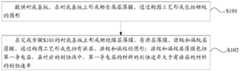
- the above preparation methodmay include the following steps S101 and S102.
- Step S101providing a substrate 1 , forming a gate metal film on the substrate 1 , and forming a pattern including the gate 2 by a patterning process;
- Step S102forming a gate insulating film on the base substrate 1 completed in step S101, and actively a thin film, a source and a drain layer film, a pattern including an active layer 4, a source 5a and a drain 5b formed by a patterning process; the source and drain layer films comprise a first conductive layer film, corresponding etching In the liquid, the etching rate of the material of the first conductive layer film is greater than the etching rate of the material of the active layer 4.
- step S101as an example and then performing step S102 as an example.
- step S102may also be performed before step S101.
- the step S102when the source/drain electrode layer formed on the active layer is etched to form the source 5a and the drain 5b, the first conductive layer is in the corresponding etching liquid.
- the etching rate of the material of the thin filmis greater than the etching rate of the material of the active layer 4, and the difference in etching rate can reduce the damage of the active layer 4 by the etching process in forming the source 5a and the drain 5b, and therefore, Set the etch barrier.
- step S102may include: on the base substrate 1 (for example, the lining may be completed in step S101) a gate insulating layer film, an active layer film, a source and a drain layer film are formed on the base substrate), and a pattern including the active layer 4, the source 5a and the drain 5b is formed by a patterning process; the source and drain layers are formed
- the first conductive layer film and the second conductive layer film formed on the first conductive layer filmwherein in the corresponding etching liquid, the etching rate of the material of the first conductive layer film is greater than the material of the active layer 4
- the etching rate of the second conductive layer filmis greater than the conductivity of the first conductive layer film.
- step S102when the source/drain electrode layer formed on the active layer is etched to form the source 5a and the drain 5b, the second conductive layer 51 is first etched, and then The first conductive layer 52 is etched. Therefore, as long as the etching rate of the material of the first conductive layer 52 is greater than the etching rate of the material of the active layer 4 in the corresponding etching liquid, the difference in etching rate can be utilized.
- the material of the active layermay be an oxide semiconductor such as indium gallium zinc oxide.
- the preparation material of the first conductive layer 52may include ZnON (oxygen-doped zinc nitride), ZnO doped with a small amount of elements such as Ga, Si, Ge, Ti, Hf, Y, Zr, F (ie, GaZnO, SiZnO, One or more of GeZnO, TiZnO, HfZnO, YZnO, ZrZnO, FZnO), CdO and its doping system (such as InCdO, etc.).
- ZnONoxygen-doped zinc nitride
- ZnO doped with a small amount of elementssuch as Ga, Si, Ge, Ti, Hf, Y, Zr, F (ie, GaZnO, SiZnO, One or more of GeZnO, TiZnO, HfZnO, YZnO, ZrZnO, FZnO), CdO and its doping system (such as InCdO, etc.).
- the material of the second conductive layer 51may include one or more of Mo, Al, Ti, and Cu. kind.
- a pattern including the active layer 4, the source 5a, and the drain 5bmay be formed by a plurality of patterning processes.
- the active layer filmis patterned by a first patterning process using a common mask to form a pattern of the active layer 4; then, the source and drain layers are processed by a second patterning process using a common mask.
- the filmis patterned to form a pattern of source 5a and drain 5b.
- a gate insulating filmmay be sequentially deposited on the substrate 1 by a plasma enhanced chemical vapor deposition method.
- a thin film, an active layer film, a source and a drain filmare deposited by magnetron sputtering or thermal evaporation, and then the active layer film is patterned by a first patterning process using a common mask to form an active layer.
- the pattern of layer 4; as shown in Fig. 3b, the source and drain layer filmsare then patterned by a second patterning process using a conventional mask to form a pattern of source 5a and drain 5b.
- the embodiments of the present inventioninclude, but are not limited to, the following.
- a gate insulating filmmay be formed on the patterns of the source and drain after forming the pattern of the source and the drain.
- a pattern including the active layer 4, the source 5a, and the drain 5bmay be formed by one patterning process.
- a layer of photoresist 7is coated on the source and drain layer films; It is shown that the photoresist 7 is formed by a two-tone mask or a gray-scale mask, so that the photoresist 7 forms a photoresist completely removed region, a photoresist completely reserved region, and a photoresist semi-reserved region; a region where a gap between the patterns of the source 5a and the drain 5b is located, a region where the photoresist completely remains corresponds to a region of the pattern of the active layer 4 other than the slit, and a photoresist completely removed region corresponds to the active layer The area other than 4; after the development process, the thickness of the photoresist in the completely remaining area of the photoresist does
- the source and drain layer films and the active layer film in the completely removed region of the photoresistare completely etched away by the first etching process to form a pattern including the active layer 4; as shown in FIG. 4b, The process removes the photoresist in the semi-reserved region of the photoresist.
- the source and drain layer films of the regionare removed; the second conductive layer film in the source and drain layer films of the semi-reserved region of the photoresist is completely etched by the second etching process; The etching process completely etches away the first conductive layer film in the source and drain layer films of the semi-reserved region of the photoresist to form a pattern including the source 5a and the drain 5b; and peels off the remaining photoresist 7.
- a gate insulating layer film and an active layer filmmay be sequentially deposited on the substrate substrate by a plasma enhanced chemical vapor deposition method, and employed.
- a magnetron sputtering or thermal evaporation methoddeposits a source and drain layer film on the active layer film.
- the embodiments of the present inventioninclude, but are not limited to, the following.
- a gate insulating filmmay be formed on the patterns of the source and drain after forming the pattern of the source and the drain.
- the second etching processmay employ dry etching; the third etching process may employ wet etching. That is, the first conductive layer 51 formed by the metal material is processed by a dry etching process, and the first conductive layer 52 is processed by a wet etching process using the corresponding etching solution to ensure the second conductive layer 51 and the first The accuracy of the conductive layer 52 when etched.
- the etching solution of the above wet etching processmay be an acidic solution or an alkaline solution.
- the etching solution of the above wet etching processmay be a hydrochloric acid solution, a formic acid solution, an acetic acid solution, a tetramethylammonium hydroxide (TMAH) solution, a sodium hydroxide solution or a potassium hydroxide solution.
- TMAHtetramethylammonium hydroxide
- At least one embodiment of the present inventionalso provides an array substrate comprising the thin film transistor provided in any of the above embodiments.
- the array substrate provided in the embodiment of the present inventionmay be any type of array substrate, as long as the array substrate includes the thin film transistor provided in any of the above embodiments.
- the array substratemay be an array substrate for a liquid crystal display device, in which case the array substrate further includes a pixel electrode.
- the array substratecan also include a common electrode.
- the array substratemay be used for an OLED array substrate, in which case the array substrate further includes OLED units arranged in a matrix, each OLED unit including, for example, an anode, a cathode, and a light emitting layer disposed therebetween .
- the array substrate provided by the embodiment of the present inventionfurther includes a plurality of gate lines and a plurality of data lines crossing each other, and other structures, which are not described herein.
- At least one embodiment of the present inventionfurther provides a display device, which may include the array substrate in the above embodiment.
- the display devicehas a low number of patterning processes and low cost.
- the display deviceincludes a liquid crystal panel, an electronic paper, an OLED panel, a mobile phone, a tablet computer, a television, a display, a notebook computer, a digital photo frame, a navigator, and the like, and any product or component having a display function.
- first and second wordsare used in the present invention to perform similar items.
- the inventionis not limited by the number of the first and second words, but is merely illustrative of an alternative manner, and those skilled in the art will recognize obvious similar variations or related matters according to the disclosure of the present invention. Extensions are all within the scope of the invention.
Landscapes
- Engineering & Computer Science (AREA)
- Manufacturing & Machinery (AREA)
- Physics & Mathematics (AREA)
- Geometry (AREA)
- Microelectronics & Electronic Packaging (AREA)
- Thin Film Transistor (AREA)
Abstract
Description
Translated fromChinese本发明实施例涉及一种薄膜晶体管及其制备方法、阵列基板、显示装置。Embodiments of the present invention relate to a thin film transistor, a method of fabricating the same, an array substrate, and a display device.
新兴的以铟镓锌氧化物(Indium-Gallium-Zinc Oxide,IGZO)薄膜晶体管(Thin Film Transistor,TFT)为代表的金属氧化物半导体TFT技术因兼具多晶硅TFT和非晶硅TFT的优点,被认为是下一代显示技术中最具潜力的器件。尤其在TFT面板的制备方面,由于IGZO TFT与非晶硅TFT采用类似的器件结构并可以低温制备,因此,IGZO TFT的制备工艺可以与非晶硅TFT的生产工艺相互兼容,即可以采用工艺过程简单、成本低的背沟道刻蚀(Back Channel Etch,BCE)工艺。The emerging metal oxide semiconductor TFT technology represented by Indium-Gallium-Zinc Oxide (IGZO) Thin Film Transistor (TFT) has the advantages of both polysilicon TFT and amorphous silicon TFT. It is considered to be the most promising device in the next generation of display technology. Especially in the preparation of the TFT panel, since the IGZO TFT and the amorphous silicon TFT adopt a similar device structure and can be prepared at a low temperature, the preparation process of the IGZO TFT can be compatible with the production process of the amorphous silicon TFT, that is, the process can be employed. Simple, low cost Back Channel Etch (BCE) process.
发明内容Summary of the invention
本发明实施例提供了一种薄膜晶体管及其制备方法、阵列基板、显示装置,用以实现一种新的背沟道TFT结构,以简化基于氧化物半导体TFT的制作工艺。Embodiments of the present invention provide a thin film transistor, a method for fabricating the same, an array substrate, and a display device for implementing a novel back channel TFT structure to simplify a fabrication process based on an oxide semiconductor TFT.
本发明的至少一个实施例提供了一种薄膜晶体管,其包括栅极、有源层、源极和漏极,所述源极和漏极包括设置于有源层上的第一导电层;在对应的刻蚀液中,所述第一导电层的材料的刻蚀速率大于所述有源层的材料的刻蚀速率。At least one embodiment of the present invention provides a thin film transistor including a gate, an active layer, a source and a drain, the source and the drain including a first conductive layer disposed on the active layer; In the corresponding etching solution, the etching rate of the material of the first conductive layer is greater than the etching rate of the material of the active layer.
本发明的至少一个实施例还提供了一种薄膜晶体管的制备方法,其包括:提供衬底基板,在所述衬底基板上形成栅金属层薄膜,通过构图工艺形成包括栅极的图形;以及在所述衬底基板上形成栅绝缘层薄膜、有源层薄膜、源极和漏极层薄膜,通过构图工艺形成包括有源层、源极和漏极的图形;所述源极和漏极层薄膜包括第一导电层薄膜,在对应的刻蚀液中,所述第一导电层薄膜的材料的刻蚀速率大于所述有源层的材料的刻蚀速率。At least one embodiment of the present invention also provides a method of fabricating a thin film transistor, comprising: providing a substrate on which a gate metal layer film is formed, and forming a pattern including a gate by a patterning process; Forming a gate insulating layer film, an active layer film, a source and a drain layer film on the base substrate, and forming a pattern including an active layer, a source and a drain by a patterning process; the source and the drain The layer film comprises a first conductive layer film, and in the corresponding etching liquid, the etching rate of the material of the first conductive layer film is greater than the etching rate of the material of the active layer.
本发明的至少一个实施例还提供了一种阵列基板,该阵列基板包括上述技术方案中提供的薄膜晶体管。At least one embodiment of the present invention also provides an array substrate including the aboveA thin film transistor provided in the technical solution.
本发明的至少一个实施例还提供一种显示装置,该显示装置包括上述技术方案中所述的阵列基板。At least one embodiment of the present invention also provides a display device including the array substrate described in the above technical solution.
为了更清楚地说明本发明实施例的技术方案,下面将对实施例的附图作简单地介绍,显而易见地,下面描述中的附图仅仅涉及本发明的一些实施例,而非对本发明的限制。In order to more clearly illustrate the technical solutions of the embodiments of the present invention, the drawings of the embodiments will be briefly described below. It is obvious that the drawings in the following description relate only to some embodiments of the present invention, and are not intended to limit the present invention. .
图1a为本发明实施例提供的薄膜晶体管的结构示意图;1a is a schematic structural diagram of a thin film transistor according to an embodiment of the present invention;
图1b为本发明另一实施例提供的薄膜晶体管的结构示意图;FIG. 1b is a schematic structural diagram of a thin film transistor according to another embodiment of the present invention; FIG.
图2为本发明实施例提供的薄膜晶体管的制备方法的流程图;2 is a flowchart of a method for fabricating a thin film transistor according to an embodiment of the present invention;
图3a为本发明实施例提供的薄膜晶体管的制备方法中经过第一次构图工艺形成有源层后的结构示意图;3a is a schematic structural view of a method for fabricating a thin film transistor according to an embodiment of the present invention, after forming an active layer by a first patterning process;
图3b为本发明实施例提供的薄膜晶体管的制备方法中经过第二次构图工艺形成源极和漏极后的结构示意图;3b is a schematic structural view of a method for fabricating a thin film transistor according to an embodiment of the present invention, after forming a source and a drain through a second patterning process;
图4a为本发明另一实施例提供的薄膜晶体管的制备方法中经过第一次构图工艺形成包括有源层的图形后的结构示意图;4a is a schematic structural view of a method for fabricating a thin film transistor according to another embodiment of the present invention, after forming a pattern including an active layer by a first patterning process;
图4b为本发明另一实施例提供的薄膜晶体管的制备方法中经过第二次构图工艺形成包括源极和漏极的图形后的结构示意图。4b is a schematic structural view of a method for fabricating a thin film transistor according to another embodiment of the present invention, after forming a pattern including a source and a drain through a second patterning process.
为使本发明实施例的目的、技术方案和优点更加清楚,下面将结合本发明实施例的附图,对本发明实施例的技术方案进行清楚、完整地描述。显然,所描述的实施例是本发明的一部分实施例,而不是全部的实施例。基于所描述的本发明的实施例,本领域普通技术人员在无需创造性劳动的前提下所获得的所有其他实施例,都属于本发明保护的范围。The technical solutions of the embodiments of the present invention will be clearly and completely described in the following with reference to the accompanying drawings. It is apparent that the described embodiments are part of the embodiments of the invention, and not all of the embodiments. All other embodiments obtained by a person of ordinary skill in the art based on the described embodiments of the present invention without departing from the scope of the invention are within the scope of the invention.
在研究中,本申请的发明人注意到,由于IGZO化学稳定性较差,其作为有源层的材料时,易被刻蚀液损伤,从而使IGZO TFT的BCE制造工艺难以实现。In the study, the inventors of the present application have noticed that since IGZO is poor in chemical stability, it is easily damaged by an etching liquid when it is used as a material of an active layer, thereby making it difficult to realize a BCE manufacturing process of IGZO TFT.
本发明实施例提供一种薄膜晶体管,包括有源层、源极和漏极,源极和漏极包括设置于有源层上的第一导电层;在对应的刻蚀液(用于对形成源极和漏极的材料进行刻蚀的刻蚀液)中,第一导电层的材料的刻蚀速率大于有源层的材料的刻蚀速率。Embodiments of the present invention provide a thin film transistor including an active layer, a source and a drain, and a source andThe drain includes a first conductive layer disposed on the active layer; and a corresponding etchant (an etchant for etching a material forming the source and the drain), the material of the first conductive layer The etch rate is greater than the etch rate of the material of the active layer.
上述薄膜晶体管中,源极和漏极包括设置于有源层上的第一导电层,且第一导电层的材料的刻蚀速率大于有源层材料的刻蚀速率,因此,利用第一导电层和有源层刻蚀速率的差异在刻蚀源极和漏极的过程中可以减小刻蚀工艺对有源层的损伤,从而可以解决薄膜晶体管的有源层易被源极和漏极形成工序中使用的刻蚀液腐蚀的问题。因此,本发明实施例提供的薄膜晶体管可以使用背沟道刻蚀工艺制造而无需设置刻蚀阻挡层,从而可以减少构图工艺次数,降低制造成本。因此,当本发明实施例提供的TFT的有源层为易腐蚀的氧化物半导体材料时,也可以使用背沟道刻蚀工艺制造,从而可以简化氧化物半导体TFT的制作工艺。In the above thin film transistor, the source and the drain include a first conductive layer disposed on the active layer, and an etch rate of the material of the first conductive layer is greater than an etch rate of the active layer material, and thus, the first conductive is utilized The difference in etch rate between the layer and the active layer can reduce the damage of the active layer by the etching process during the process of etching the source and the drain, thereby solving the problem that the active layer of the thin film transistor is easily affected by the source and the drain. The problem of etching of the etching solution used in the forming process. Therefore, the thin film transistor provided by the embodiment of the present invention can be fabricated by using a back channel etching process without providing an etch barrier layer, thereby reducing the number of patterning processes and reducing the manufacturing cost. Therefore, when the active layer of the TFT provided by the embodiment of the present invention is an easily corrodible oxide semiconductor material, it can also be fabricated using a back channel etching process, thereby simplifying the fabrication process of the oxide semiconductor TFT.
如图1a所示,本发明的至少一个实施例提供的一种薄膜晶体管包括栅极2、有源层4、以及彼此间隔开的源极5a和漏极5b(源极5a和漏极5b的位置可互换),源极5a和漏极5b包括设置在有源层4上的第一导电层52;在对应的刻蚀液中,第一导电层52的材料的刻蚀速率大于有源层4的材料的刻蚀速率。As shown in FIG. 1a, at least one embodiment of the present invention provides a thin film transistor including a
例如,沿垂直于有源层4所在面的方向上,第一导电层52与有源层4之间未设置绝缘层(即,第一导电层52与有源层4直接接触)。本发明实施例可以应用于背沟道刻蚀工艺制造的薄膜晶体管,即,在该薄膜晶体管中,源极5a和漏极5b在有源层4形成之后形成,并且源极5a和漏极5b与有源层4直接接触。For example, in a direction perpendicular to the face of the
针对本领域中薄膜晶体管的有源层易被形成源极和漏极的工序中使用的刻蚀液腐蚀的问题,本发明实施例提供一种薄膜晶体管,在该薄膜晶体管中,源极5a和漏极5b被设置为包括第一导电层52,并且第一导电层52的材料在对应刻蚀液中的刻蚀速率大于有源层4材料的刻蚀速率。由于第一导电层52的材料在对应刻蚀液中的刻蚀速率大于有源层4的材料的刻蚀速率,利用刻蚀速率的差异能够减小有源层4在背沟道刻蚀工艺中受到的损伤,从而可以使用背沟道刻蚀工艺制造薄膜晶体管而无需刻蚀阻挡层,并且可以减少构图工艺次数,降低制造成本。The present invention provides a thin film transistor in which a
如图1b所示,例如,在上述薄膜晶体管中,源极和漏极还可以包括设置在第一导电层52上的第二导电层51,且第二导电层的导电性大于第一导电层的导电性。As shown in FIG. 1b, for example, in the above thin film transistor, the source and the drain may further include a second
上述薄膜晶体管中,由于第二导电层51的导电性大于第一导电层52的导电性,所以源极5a和漏极5b的导电性不会受第一导电层52的材料选取的影响,从而可以保持很好的整体导电性能。另外,由于导电性较好的第二导电层51与有源层4之间间隔有第一导电层52,所以,第二导电层51的材料不易扩散到有源层4中影响有源层4性能。In the above thin film transistor, since the conductivity of the second
例如,为了提高源极5a和漏极5b的整体导电性而设置的第二导电层51可以包括至少一种材料,且该至少一种材料的导电性大于第一导电层52的材料的导电性。例如,该至少一种材料可以选取高导电材料。For example, the second
另外,上述第二导电层51的具体成膜方式不做限定,例如,可以上述的至少两种高导电材料形成混合材料薄膜;也可以多层膜叠加,每一层膜为一种高导电材料形成;也可以单层膜层,由一种高导电材料形成。In addition, the specific film forming manner of the second
上述薄膜晶体管中的源极5a和漏极5b包括设置于有源层4上的第一导电层52以及设置在第一导电层52上的第二导电层51;由于在形成源极5a和漏极5b的图形的刻蚀的过程中,首先需要将上述第二导电层51进行刻蚀,然后才对第一导电层52进行刻蚀,因此,在对第二导电层51进行刻蚀时不会对有源层4处于沟道处的部位造成损伤,只要在对应的刻蚀液中,第一导电层52的材料的刻蚀速率大于有源层4材料的刻蚀速率,就能利用刻蚀速率的差异在刻蚀源极5a和漏极5b的过程中减小刻蚀工艺对有源层4的损伤;上述薄膜晶体管中,由于第二导电层51的材料的导电性大于第一导电层52的材料的导电性,所以形成的源极5a和漏极5b的导电性不会降低,整体导电性能较好;另外,由于第二导电层51与有源层4之间间隔有第一导电层52,所以,第二导电层51的材料不易扩散到有源层4中。综上,上述薄膜晶体管可以使用背沟道刻蚀工艺,并且该薄膜晶体管整体性能较高。The
例如,在至少一种具体实施方式公开的薄膜晶体管中,有源层4的制备材料可以包括氧化物半导体。For example, in the thin film transistor disclosed in at least one embodiment, the material for preparing the
例如,源极5a和漏极5b中的第一导电层52的制备材料可以包括ZnON(掺氧的氮化锌),掺杂少量Ga、Si、Ge、Ti、Hf、Y、Zr、F等元素的ZnO(即GaZnO、SiZnO、GeZnO、TiZnO、HfZnO、YZnO、ZrZnO、FZnO),以及CdO及其掺杂体系(如InCdO等)中的一种或几种。For example, the preparation material of the first
例如,源极5a和漏极5b中的第二导电层51的材料可以包括钼(Mo)、铝(Al)、钛(Ti)或者铜(Cu)中的一种或几种。For example, the material of the second
在大尺寸面板的制程中,为了降低电阻,一般采用Cu布线,然而Cu作为源极5a和漏极5b的材料很容易向氧化物半导体形成的有源层4中扩散,而本实施例中,源极5a和漏极5b中的第一导电层52可以有效阻挡Cu材料层向有源层4材料中的扩散,因此有利于提高薄膜晶体管器件的性能。In the process of a large-sized panel, in order to reduce the resistance, Cu wiring is generally used, but Cu as a material of the
刻蚀工艺中使用的刻蚀液包括酸性溶液或碱性溶液,根据第一导电层52的材料和有源层4的材料在对应刻蚀液中的刻蚀速率差,本领域技术人员可以选择合理浓度的酸性溶液或碱性溶液,以减少刻蚀工艺对有源层4的损伤。The etching solution used in the etching process includes an acidic solution or an alkaline solution, and those skilled in the art can select according to the difference in the etching rate of the material of the first
例如,上述薄膜晶体管的有源层4的材料为铟镓锌氧化物;刻蚀液包括稀释的盐酸、甲酸、乙酸或四甲基氢氧化铵、甲酸溶液、乙酸溶液、四甲基氢氧化铵(TMAH)溶液、氢氧化钠溶液或者氢氧化钾溶液中的一种或几种,根据第一导电层52的材料和有源层4的材料在对应刻蚀液中的刻蚀速率差,本领域技术人员可以选择合理浓度的酸性溶液或碱性溶液,以减少刻蚀工艺对有源层4的损伤。For example, the material of the
例如,上述薄膜晶体管可以为底栅型,在这种情况下,该薄膜晶体管的栅极设置于有源层的远离源极/漏极的一侧。例如,如图1a所示,薄膜晶体管包括形成于衬底基板1上的栅极2、形成于栅极2背离衬底基板1一侧的栅绝缘层3、上述有源层4形成于栅绝缘层3上,源极5a和漏极5b形成于有源层4上,在源极和漏极5上可以形成有钝化层6,钝化层6上形成源极5a和漏极5b的接触过孔。For example, the thin film transistor may be of a bottom gate type, in which case the gate of the thin film transistor is disposed on a side of the active layer away from the source/drain. For example, as shown in FIG. 1a, the thin film transistor includes a
例如,上述薄膜晶体管也可以为顶栅型,在这种情况下,该薄膜晶体管的栅极设置于有源层的靠近源极/漏极的一侧。For example, the thin film transistor may be of a top gate type. In this case, the gate of the thin film transistor is disposed on a side of the active layer close to the source/drain.
相对应地,本发明的至少一个实施例还提供一种薄膜晶体管的制备方法,如图2所示,上述制备方法可以包括以下步骤S101和步骤S102。Correspondingly, at least one embodiment of the present invention further provides a method for fabricating a thin film transistor. As shown in FIG. 2, the above preparation method may include the following steps S101 and S102.
步骤S101,提供衬底基板1,在衬底基板1上形成栅金属层薄膜,通过构图工艺形成包括栅极2的图形;Step S101, providing a
步骤S102,在完成步骤S101的衬底基板1上形成栅绝缘层薄膜、有源层薄膜、源极和漏极层薄膜,通过构图工艺形成包括有源层4、源极5a和漏极5b的图形;源极和漏极层薄膜包括第一导电层薄膜,在对应的刻蚀液中,第一导电层薄膜的材料的刻蚀速率大于有源层4的材料的刻蚀速率。Step S102, forming a gate insulating film on the
以上制备方法以先进行步骤S101后进行步骤S102为例进行说明。本发明实施例包括、但不限于此,例如,步骤S102也可以在步骤S101之前进行。The above preparation method will be described by taking step S101 as an example and then performing step S102 as an example. The embodiment of the present invention includes, but is not limited to, for example, step S102 may also be performed before step S101.
上述薄膜晶体管的制备方法中,步骤S102中在对位于有源层上形成的源漏电极层进行刻蚀以形成源极5a和漏极5b时,由于在对应刻蚀液中,第一导电层薄膜的材料的刻蚀速率大于有源层4材料的刻蚀速率,利用刻蚀速率的差异可以减少形成源极5a和漏极5b过程中的刻蚀工艺对有源层4损伤,因此,无需设置刻蚀阻挡层。In the above method of fabricating a thin film transistor, in the step S102, when the source/drain electrode layer formed on the active layer is etched to form the
在至少一种具体的实施例中,如图3a、图3b、图4a和图4b所示,上述制备方法中,步骤S102可以包括:在衬底基板1(例如,可以是完成步骤S101的衬底基板)上形成栅绝缘层薄膜、有源层薄膜、源极和漏极层薄膜,通过构图工艺形成包括有源层4、源极5a和漏极5b的图形;源极和漏极层薄膜包括第一导电层薄膜和形成于第一导电层薄膜上的第二导电层薄膜,其中,在对应的刻蚀液中,第一导电层薄膜的材料的刻蚀速率大于有源层4的材料的刻蚀速率,第二导电层薄膜的导电性大于第一导电层薄膜的导电性。In at least one specific embodiment, as shown in FIG. 3a, FIG. 3b, FIG. 4a and FIG. 4b, in the above preparation method, step S102 may include: on the base substrate 1 (for example, the lining may be completed in step S101) a gate insulating layer film, an active layer film, a source and a drain layer film are formed on the base substrate), and a pattern including the
上述薄膜晶体管的制备方法中,步骤S102中在对位于有源层上形成的源漏电极层进行刻蚀以形成源极5a和漏极5b时,首先对第二导电层51进行刻蚀,然后对第一导电层52进行刻蚀,因此,只要在对应刻蚀液中,第一导电层52的材料的刻蚀速率大于有源层4材料的刻蚀速率,就能利用刻蚀速率的差异减少刻蚀工艺对有源层4损伤,无需设置刻蚀阻挡层,并且,由于第二导电层51的导电性大于第一导电层52的导电性,所以源极5a和漏极5b的导电性不会降低,整体导电性能较好。In the above method of fabricating a thin film transistor, in step S102, when the source/drain electrode layer formed on the active layer is etched to form the
例如,有源层的材料可以为氧化物半导体,例如铟镓锌氧化物。For example, the material of the active layer may be an oxide semiconductor such as indium gallium zinc oxide.
例如,第一导电层52的制备材料可以包括ZnON(掺氧的氮化锌)、掺杂少量Ga、Si、Ge、Ti、Hf、Y、Zr、F等元素的ZnO(即GaZnO、SiZnO、GeZnO、TiZnO、HfZnO、YZnO、ZrZnO、FZnO),CdO及其掺杂体系(如InCdO等)中的一种或几种。For example, the preparation material of the first
例如,第二导电层51的材料可以包括Mo、Al、Ti和Cu中的一种或几种。For example, the material of the second
例如,在步骤S102中,可以通过多次构图工艺形成包括有源层4、源极5a和漏极5b的图形。例如,采用普通掩膜板通过第一次构图工艺对有源层薄膜进行图形化以形成有源层4的图形;之后,采用普通掩膜板通过第二次构图工艺对源极和漏极层薄膜进行图形化以形成源极5a和漏极5b的图形。For example, in step S102, a pattern including the
如图3a和图3b所示,在至少一种具体的实施例中,上述步骤S102中,如图3a所示,可先采用等离子体增强化学气相沉积方法依次在衬底基板1上沉积栅绝缘层薄膜、有源层薄膜、采用磁控溅射或热蒸发方法沉积源极和漏极层薄膜,然后采用普通掩膜板通过第一次构图工艺对有源层薄膜进行图形化以形成有源层4的图形;如图3b所示,然后采用普通掩膜板通过第二次构图工艺对源极和漏极层薄膜进行图形化以形成源极5a和漏极5b的图形。当然,本发明实施例包括、但不限于此。例如,也可以在形成源极和漏极的图形之后,在源极和漏极的图形上形成栅绝缘层薄膜。As shown in FIG. 3a and FIG. 3b, in at least one specific embodiment, in the above step S102, as shown in FIG. 3a, a gate insulating film may be sequentially deposited on the
例如,在步骤S102中,可以通过一次构图工艺形成包括有源层4、源极5a和漏极5b的图形。例如,如图4a和图4b所示,在另一种具体的实施例中,上述步骤S102中,在所述源极和漏极层薄膜上涂覆一层光刻胶7;如图4a所示,采用双色调掩膜版或灰阶掩膜版曝光,使光刻胶7形成光刻胶完全去除区域、光刻胶完全保留区域和光刻胶半保留区域;光刻胶半保留区域对应源极5a和漏极5b的图形之间的缝隙所在区域,光刻胶完全保留区域对应所述缝隙以外的有源层4的图形所在区域,光刻胶完全去除区域对应于所述有源层4以外的区域;显影处理后,光刻胶完全保留区域的光刻胶厚度没有发生变化,光刻胶完全去除区域的光刻胶被完全去除,光刻胶半保留区域的光刻胶厚度减小;通过第一次刻蚀工艺完全刻蚀掉光刻胶完全去除区域的源极和漏极层薄膜和有源层薄膜,形成包括有源层4的图形;如图4b所示,通过灰化工艺去除光刻胶半保留区域的光刻胶,暴露出该区域的源极和漏极层薄膜;通过第二次刻蚀工艺完全刻蚀掉光刻胶半保留区域的源极和漏极层薄膜中的第二导电层薄膜;通过第三次刻蚀工艺完全刻蚀掉光刻胶半保留区域的源极和漏极层薄膜中的第一导电层薄膜,形成包括源极5a和漏极5b的图形;剥离剩余光刻胶7。通过上述方法可以减少掩模板的使用数量、且减少光刻胶的涂覆次数,从而可以简化制备工艺。For example, in step S102, a pattern including the
例如,在图4a和图4b所示的情形中,在涂覆光刻胶7之前,可以采用等离子体增强化学气相沉积方法依次在衬底基板沉积栅绝缘层薄膜和有源层薄膜,并采用磁控溅射或热蒸发方法在有源层薄膜上沉积源极和漏极层薄膜。当然,本发明实施例包括、但不限于此。例如,也可以在形成源极和漏极的图形之后,在源极和漏极的图形上形成栅绝缘层薄膜。For example, in the case shown in FIGS. 4a and 4b, before the
在至少一种优选实施方式中,上述实施例的制备工艺中,第二次刻蚀工艺可以采用干法刻蚀;第三次刻蚀工艺可以采用湿法刻蚀。即先进行干法刻蚀工艺处理金属材料形成的第二导电层51,再使用对应的刻蚀液进行湿法刻蚀工艺处理第一导电层52,以保证对第二导电层51和第一导电层52刻蚀时的精度。In at least one preferred embodiment, in the preparation process of the above embodiment, the second etching process may employ dry etching; the third etching process may employ wet etching. That is, the first
例如,上述湿法刻蚀工艺的刻蚀液可以为酸性溶液或者碱性溶液。For example, the etching solution of the above wet etching process may be an acidic solution or an alkaline solution.
例如,上述湿法刻蚀工艺的刻蚀液可以是盐酸溶液、甲酸溶液、乙酸溶液、四甲基氢氧化铵(TMAH)溶液、氢氧化钠溶液或者氢氧化钾溶液。For example, the etching solution of the above wet etching process may be a hydrochloric acid solution, a formic acid solution, an acetic acid solution, a tetramethylammonium hydroxide (TMAH) solution, a sodium hydroxide solution or a potassium hydroxide solution.
本发明的至少一个实施例还提供一种阵列基板,该阵列基板包括上述任意一实施例中提供的薄膜晶体管。At least one embodiment of the present invention also provides an array substrate comprising the thin film transistor provided in any of the above embodiments.
本发明实施例提供的阵列基板可以为任意类型的阵列基板,只要该阵列基板包括以上任一实施例提供的薄膜晶体管即可。The array substrate provided in the embodiment of the present invention may be any type of array substrate, as long as the array substrate includes the thin film transistor provided in any of the above embodiments.
例如,该阵列基板可以为用于液晶显示装置的阵列基板,在这种情况下,该阵列基板还包括像素电极。在一些示例中,该阵列基板还可以包括公共电极。For example, the array substrate may be an array substrate for a liquid crystal display device, in which case the array substrate further includes a pixel electrode. In some examples, the array substrate can also include a common electrode.
例如,该阵列基板可以为用于OLED阵列基板,在这种情况下,该阵列基板还包括呈矩阵排列的OLED单元,每个OLED单元例如包括阳极、阴极以及设置于二者之间的发光层。For example, the array substrate may be used for an OLED array substrate, in which case the array substrate further includes OLED units arranged in a matrix, each OLED unit including, for example, an anode, a cathode, and a light emitting layer disposed therebetween .
当然,本发明实施例提供的阵列基板还包括相互交叉的多条栅线和多条数据线,以及其它结构,此处不做赘述。Of course, the array substrate provided by the embodiment of the present invention further includes a plurality of gate lines and a plurality of data lines crossing each other, and other structures, which are not described herein.
本发明的至少一个实施例还提供一种显示装置,该显示装置可以包括:上述实施例中的阵列基板。该显示装置的构图工艺次数少,成本低。该显示装置包括液晶面板、电子纸、OLED面板、手机、平板电脑、电视机、显示器、笔记本电脑、数码相框、导航仪等任何具有显示功能的产品或部件。At least one embodiment of the present invention further provides a display device, which may include the array substrate in the above embodiment. The display device has a low number of patterning processes and low cost. The display device includes a liquid crystal panel, an electronic paper, an OLED panel, a mobile phone, a tablet computer, a television, a display, a notebook computer, a digital photo frame, a navigator, and the like, and any product or component having a display function.
为了便于清楚说明,在本发明中采用了第一、第二等字样对相似项进行类别区分,该第一、第二字样并不在数量上对本发明进行限制,只是对一种可选的方式的举例说明,本领域技术人员根据本发明公开的内容,想到的显而易见的相似变形或相关扩展均属于本发明的保护范围内。In order to facilitate the clear description, the first and second words are used in the present invention to perform similar items.The invention is not limited by the number of the first and second words, but is merely illustrative of an alternative manner, and those skilled in the art will recognize obvious similar variations or related matters according to the disclosure of the present invention. Extensions are all within the scope of the invention.
显然,本领域的技术人员可以对本发明实施例进行各种改动和变型而不脱离本发明的精神和范围。这样,倘若本发明的这些修改和变型属于本发明权利要求及其等同技术的范围之内,则本发明也意图包含这些改动和变型在内。It is apparent that those skilled in the art can make various modifications and variations to the embodiments of the invention without departing from the spirit and scope of the invention. Thus, it is intended that the present invention cover the modifications and modifications of the invention
本申请要求于2015年6月24日递交的中国专利申请第201510354328.8号的优先权,在此全文引用上述中国专利申请公开的内容以作为本申请的一部分。The present application claims the priority of the Chinese Patent Application No. 201510354328.8 filed on Jun. 24, 2015, the entire disclosure of which is hereby incorporated by reference.
Claims (19)
Translated fromChinesePriority Applications (1)
| Application Number | Priority Date | Filing Date | Title |
|---|---|---|---|
| US15/127,262US10510901B2 (en) | 2015-06-24 | 2015-09-24 | Thin film transistor and fabrication method thereof, array substrate and display device |
Applications Claiming Priority (2)
| Application Number | Priority Date | Filing Date | Title |
|---|---|---|---|
| CN201510354328.8ACN105097943A (en) | 2015-06-24 | 2015-06-24 | Thin film transistor and manufacturing method thereof, array substrate and display device |
| CN201510354328.8 | 2015-06-24 |
Publications (1)
| Publication Number | Publication Date |
|---|---|
| WO2016206206A1true WO2016206206A1 (en) | 2016-12-29 |
Family
ID=54577975
Family Applications (1)
| Application Number | Title | Priority Date | Filing Date |
|---|---|---|---|
| PCT/CN2015/090550CeasedWO2016206206A1 (en) | 2015-06-24 | 2015-09-24 | Thin film transistor and manufacturing method thereof, array substrate, and display device |
Country Status (3)
| Country | Link |
|---|---|
| US (1) | US10510901B2 (en) |
| CN (1) | CN105097943A (en) |
| WO (1) | WO2016206206A1 (en) |
Families Citing this family (12)
| Publication number | Priority date | Publication date | Assignee | Title |
|---|---|---|---|---|
| CN105655354A (en)* | 2016-01-22 | 2016-06-08 | 京东方科技集团股份有限公司 | Thin film transistor, array substrate and preparation method thereof and display device |
| CN106024705B (en)* | 2016-06-01 | 2019-04-30 | 深圳市华星光电技术有限公司 | Manufacturing method of TFT substrate |
| CN107836039A (en)* | 2016-11-23 | 2018-03-23 | 深圳市柔宇科技有限公司 | The manufacture method of array base palte |
| CN108681167B (en)* | 2018-06-22 | 2021-09-03 | 厦门天马微电子有限公司 | Display panel and display device |
| CN109378271B (en)* | 2018-10-22 | 2021-01-26 | 京东方科技集团股份有限公司 | Patterned metal film layer, thin film transistor, and preparation method of display substrate |
| GB2582974A (en)* | 2019-04-12 | 2020-10-14 | Flexenable Ltd | Organic semiconductor transistors |
| CN111403337A (en)* | 2020-03-31 | 2020-07-10 | 成都中电熊猫显示科技有限公司 | Array substrate, display panel and manufacturing method of array substrate |
| CN114256356A (en)* | 2020-09-24 | 2022-03-29 | 咸阳虹微新型显示技术有限公司 | Thin film transistor, display panel, display and preparation method of thin film transistor |
| CN112928027A (en)* | 2021-02-10 | 2021-06-08 | 昆山龙腾光电股份有限公司 | Thin film transistor and manufacturing method thereof |
| CN114497231B (en)* | 2022-02-09 | 2025-06-27 | 京东方科技集团股份有限公司 | Conductive structure and preparation method thereof, transistor and preparation method thereof, and display panel |
| CN117276306A (en)* | 2022-06-10 | 2023-12-22 | 中国科学院微电子研究所 | Thin film transistor and preparation method thereof, memory and display |
| CN115939218A (en)* | 2023-01-04 | 2023-04-07 | 西湖大学 | Thin film transistor and preparation method thereof |
Citations (4)
| Publication number | Priority date | Publication date | Assignee | Title |
|---|---|---|---|---|
| CN101901787A (en)* | 2009-05-27 | 2010-12-01 | 乐金显示有限公司 | Oxide thin film transistor and method for manufacturing the same |
| US20110006300A1 (en)* | 2009-07-09 | 2011-01-13 | Fujifilm Corporation | Electronic device, method of manufacturing the same, display and sensor |
| CN102709234A (en)* | 2011-08-19 | 2012-10-03 | 京东方科技集团股份有限公司 | Thin film transistor (TFT) array substrate and manufacturing method thereof, and electronic device |
| CN103794652A (en)* | 2014-02-25 | 2014-05-14 | 华南理工大学 | Metal-oxide semiconductor thin film transistor and manufacturing method thereof |
Family Cites Families (12)
| Publication number | Priority date | Publication date | Assignee | Title |
|---|---|---|---|---|
| US20110240592A1 (en)* | 2008-10-29 | 2011-10-06 | Mitsubishi Gas Chemical Company, Inc. | Texture processing liquid for transparent conductive film mainly composed of zinc oxide and method for producing transparent conductive film having recesses and projections |
| US8367486B2 (en)* | 2009-02-05 | 2013-02-05 | Semiconductor Energy Laboratory Co., Ltd. | Transistor and method for manufacturing the transistor |
| CN101807586B (en)* | 2009-02-13 | 2013-07-31 | 北京京东方光电科技有限公司 | TFT-LCD (Thin Film Transistor Liquid Crystal Display) array substrate and manufacturing method thereof |
| US20100224880A1 (en)* | 2009-03-05 | 2010-09-09 | Semiconductor Energy Laboratory Co., Ltd. | Semiconductor device |
| KR101878750B1 (en)* | 2010-06-18 | 2018-07-17 | 삼성전자주식회사 | Monolayer graphene comprising alkali metal, and electronic device comprising the same |
| CN102156368A (en)* | 2011-01-18 | 2011-08-17 | 京东方科技集团股份有限公司 | Thin film transistor liquid crystal display (TFT-LCD) array substrate and manufacturing method thereof |
| CN102646630B (en)* | 2011-10-11 | 2014-04-02 | 京东方科技集团股份有限公司 | TFT-LCD (thin film transistor liquid crystal display) array substrate structure and manufacturing method thereof |
| CN102637591B (en) | 2012-05-03 | 2015-05-27 | 广州新视界光电科技有限公司 | Method for etching electrode layer on oxide semiconductor |
| CN102769040B (en)* | 2012-07-25 | 2015-03-04 | 京东方科技集团股份有限公司 | Thin-film transistor, array substrate, array substrate manufacturing method and display device |
| CN103337462B (en) | 2013-06-13 | 2017-03-22 | 北京大学深圳研究生院 | Preparation method of thin film transistor |
| US9882014B2 (en)* | 2013-11-29 | 2018-01-30 | Semiconductor Energy Laboratory Co., Ltd. | Semiconductor device and method for manufacturing the same |
| KR102334986B1 (en)* | 2014-12-09 | 2021-12-06 | 엘지디스플레이 주식회사 | Crystallization Method for Oxide Semiconductor Layer, Semiconductor Device and Method for Manufacturing the Same, Applying thereof |
- 2015
- 2015-06-24CNCN201510354328.8Apatent/CN105097943A/enactivePending
- 2015-09-24USUS15/127,262patent/US10510901B2/enactiveActive
- 2015-09-24WOPCT/CN2015/090550patent/WO2016206206A1/ennot_activeCeased
Patent Citations (4)
| Publication number | Priority date | Publication date | Assignee | Title |
|---|---|---|---|---|
| CN101901787A (en)* | 2009-05-27 | 2010-12-01 | 乐金显示有限公司 | Oxide thin film transistor and method for manufacturing the same |
| US20110006300A1 (en)* | 2009-07-09 | 2011-01-13 | Fujifilm Corporation | Electronic device, method of manufacturing the same, display and sensor |
| CN102709234A (en)* | 2011-08-19 | 2012-10-03 | 京东方科技集团股份有限公司 | Thin film transistor (TFT) array substrate and manufacturing method thereof, and electronic device |
| CN103794652A (en)* | 2014-02-25 | 2014-05-14 | 华南理工大学 | Metal-oxide semiconductor thin film transistor and manufacturing method thereof |
Also Published As
| Publication number | Publication date |
|---|---|
| CN105097943A (en) | 2015-11-25 |
| US10510901B2 (en) | 2019-12-17 |
| US20180175204A1 (en) | 2018-06-21 |
Similar Documents
| Publication | Publication Date | Title |
|---|---|---|
| WO2016206206A1 (en) | Thin film transistor and manufacturing method thereof, array substrate, and display device | |
| CN103489876B (en) | A kind of array base palte and preparation method thereof, display device | |
| CN103456740B (en) | Pixel cell and manufacture method, array base palte and display unit | |
| CN102636927B (en) | Array base palte and manufacture method thereof | |
| WO2015100935A1 (en) | Array substrate and method for fabrication thereof, and display device | |
| CN106783737B (en) | Array substrate and manufacturing method thereof, display panel, and display device | |
| WO2014166176A1 (en) | Thin-film transistor and manufacturing method thereof, array base plate and display apparatus | |
| WO2015100898A1 (en) | Thin-film transistor, tft array substrate and manufacturing method therefor, and display device | |
| CN103579115B (en) | Complementary thin-film transistor and preparation method thereof, array base palte, display unit | |
| CN103456742A (en) | Array substrate, manufacturing method of array substrate and display device | |
| CN103489921B (en) | A kind of thin-film transistor and manufacture method, array base palte and display unit | |
| WO2016150056A1 (en) | Thin-film transistor and manufacturing method therefor, and display device | |
| WO2016000342A1 (en) | Array substrate, manufacturing method therefor, and display apparatus | |
| WO2017166833A1 (en) | Thin-film transistor and manufacturing method thereof, array substrate, and display apparatus | |
| WO2016011727A1 (en) | Thin-film transistor and manufacturing method therefor, array substrate and display device | |
| WO2013127201A1 (en) | Array substrate, manufacturing method and display device thereof | |
| WO2016123974A1 (en) | Thin-film transistor, pixel structure, manufacturing methods therefor, array substrate and display device | |
| CN104064472A (en) | Thin film transistor, manufacturing method thereof, and display device | |
| WO2020228499A1 (en) | Transistor device and manufacturing method therefor, display substrate and display apparatus | |
| CN103489874B (en) | Array base palte and preparation method thereof, display unit | |
| CN104133313A (en) | Array substrate, manufacturing method thereof and liquid crystal display device | |
| TWI546850B (en) | Display panel preparation method | |
| WO2016026207A1 (en) | Array substrate and manufacturing method thereof, and display device | |
| CN112002636A (en) | Array substrate, preparation method thereof, and display panel | |
| CN105931985A (en) | Array substrate, preparation method therefor, and display device |
Legal Events
| Date | Code | Title | Description |
|---|---|---|---|
| WWE | Wipo information: entry into national phase | Ref document number:15127262 Country of ref document:US | |
| 121 | Ep: the epo has been informed by wipo that ep was designated in this application | Ref document number:15896101 Country of ref document:EP Kind code of ref document:A1 | |
| NENP | Non-entry into the national phase | Ref country code:DE | |
| 122 | Ep: pct application non-entry in european phase | Ref document number:15896101 Country of ref document:EP Kind code of ref document:A1 | |
| 122 | Ep: pct application non-entry in european phase | Ref document number:15896101 Country of ref document:EP Kind code of ref document:A1 | |
| 32PN | Ep: public notification in the ep bulletin as address of the adressee cannot be established | Free format text:NOTING OF LOSS OF RIGHTS PURSUANT TO RULE 112(1) EPC (EPO FORM 1205A DATED 25.06.2018) | |
| 122 | Ep: pct application non-entry in european phase | Ref document number:15896101 Country of ref document:EP Kind code of ref document:A1 |