WO2016185883A1 - Semiconductor device and imaging device - Google Patents
Semiconductor device and imaging deviceDownload PDFInfo
- Publication number
- WO2016185883A1 WO2016185883A1PCT/JP2016/063037JP2016063037WWO2016185883A1WO 2016185883 A1WO2016185883 A1WO 2016185883A1JP 2016063037 WJP2016063037 WJP 2016063037WWO 2016185883 A1WO2016185883 A1WO 2016185883A1
- Authority
- WO
- WIPO (PCT)
- Prior art keywords
- metal layer
- semiconductor chip
- layer
- insulating layer
- pad
- Prior art date
- Legal status (The legal status is an assumption and is not a legal conclusion. Google has not performed a legal analysis and makes no representation as to the accuracy of the status listed.)
- Ceased
Links
Images


Classifications
- G—PHYSICS
- G06—COMPUTING OR CALCULATING; COUNTING
- G06F—ELECTRIC DIGITAL DATA PROCESSING
- G06F30/00—Computer-aided design [CAD]
- G06F30/30—Circuit design
- G06F30/39—Circuit design at the physical level
- H—ELECTRICITY
- H01—ELECTRIC ELEMENTS
- H01L—SEMICONDUCTOR DEVICES NOT COVERED BY CLASS H10
- H01L23/00—Details of semiconductor or other solid state devices
- H01L23/52—Arrangements for conducting electric current within the device in operation from one component to another, i.e. interconnections, e.g. wires, lead frames
- H01L23/522—Arrangements for conducting electric current within the device in operation from one component to another, i.e. interconnections, e.g. wires, lead frames including external interconnections consisting of a multilayer structure of conductive and insulating layers inseparably formed on the semiconductor body
- H—ELECTRICITY
- H01—ELECTRIC ELEMENTS
- H01L—SEMICONDUCTOR DEVICES NOT COVERED BY CLASS H10
- H01L23/00—Details of semiconductor or other solid state devices
- H01L23/562—Protection against mechanical damage
- H—ELECTRICITY
- H01—ELECTRIC ELEMENTS
- H01L—SEMICONDUCTOR DEVICES NOT COVERED BY CLASS H10
- H01L23/00—Details of semiconductor or other solid state devices
- H01L23/58—Structural electrical arrangements for semiconductor devices not otherwise provided for, e.g. in combination with batteries
- H01L23/585—Structural electrical arrangements for semiconductor devices not otherwise provided for, e.g. in combination with batteries comprising conductive layers or plates or strips or rods or rings
- H—ELECTRICITY
- H01—ELECTRIC ELEMENTS
- H01L—SEMICONDUCTOR DEVICES NOT COVERED BY CLASS H10
- H01L24/00—Arrangements for connecting or disconnecting semiconductor or solid-state bodies; Methods or apparatus related thereto
- H01L24/01—Means for bonding being attached to, or being formed on, the surface to be connected, e.g. chip-to-package, die-attach, "first-level" interconnects; Manufacturing methods related thereto
- H01L24/02—Bonding areas ; Manufacturing methods related thereto
- H01L24/07—Structure, shape, material or disposition of the bonding areas after the connecting process
- H01L24/08—Structure, shape, material or disposition of the bonding areas after the connecting process of an individual bonding area
- H—ELECTRICITY
- H01—ELECTRIC ELEMENTS
- H01L—SEMICONDUCTOR DEVICES NOT COVERED BY CLASS H10
- H01L24/00—Arrangements for connecting or disconnecting semiconductor or solid-state bodies; Methods or apparatus related thereto
- H01L24/80—Methods for connecting semiconductor or other solid state bodies using means for bonding being attached to, or being formed on, the surface to be connected
- H01L24/89—Methods for connecting semiconductor or other solid state bodies using means for bonding being attached to, or being formed on, the surface to be connected using at least one connector not provided for in any of the groups H01L24/81 - H01L24/86
- H—ELECTRICITY
- H01—ELECTRIC ELEMENTS
- H01L—SEMICONDUCTOR DEVICES NOT COVERED BY CLASS H10
- H01L25/00—Assemblies consisting of a plurality of semiconductor or other solid state devices
- H01L25/03—Assemblies consisting of a plurality of semiconductor or other solid state devices all the devices being of a type provided for in a single subclass of subclasses H10B, H10D, H10F, H10H, H10K or H10N, e.g. assemblies of rectifier diodes
- H01L25/04—Assemblies consisting of a plurality of semiconductor or other solid state devices all the devices being of a type provided for in a single subclass of subclasses H10B, H10D, H10F, H10H, H10K or H10N, e.g. assemblies of rectifier diodes the devices not having separate containers
- H01L25/041—Assemblies consisting of a plurality of semiconductor or other solid state devices all the devices being of a type provided for in a single subclass of subclasses H10B, H10D, H10F, H10H, H10K or H10N, e.g. assemblies of rectifier diodes the devices not having separate containers the devices being of a type provided for in subclass H10F
- H01L25/043—Stacked arrangements of devices
- H—ELECTRICITY
- H01—ELECTRIC ELEMENTS
- H01L—SEMICONDUCTOR DEVICES NOT COVERED BY CLASS H10
- H01L25/00—Assemblies consisting of a plurality of semiconductor or other solid state devices
- H01L25/03—Assemblies consisting of a plurality of semiconductor or other solid state devices all the devices being of a type provided for in a single subclass of subclasses H10B, H10D, H10F, H10H, H10K or H10N, e.g. assemblies of rectifier diodes
- H01L25/04—Assemblies consisting of a plurality of semiconductor or other solid state devices all the devices being of a type provided for in a single subclass of subclasses H10B, H10D, H10F, H10H, H10K or H10N, e.g. assemblies of rectifier diodes the devices not having separate containers
- H01L25/065—Assemblies consisting of a plurality of semiconductor or other solid state devices all the devices being of a type provided for in a single subclass of subclasses H10B, H10D, H10F, H10H, H10K or H10N, e.g. assemblies of rectifier diodes the devices not having separate containers the devices being of a type provided for in group H10D89/00
- H01L25/0657—Stacked arrangements of devices
- H—ELECTRICITY
- H01—ELECTRIC ELEMENTS
- H01L—SEMICONDUCTOR DEVICES NOT COVERED BY CLASS H10
- H01L25/00—Assemblies consisting of a plurality of semiconductor or other solid state devices
- H01L25/03—Assemblies consisting of a plurality of semiconductor or other solid state devices all the devices being of a type provided for in a single subclass of subclasses H10B, H10D, H10F, H10H, H10K or H10N, e.g. assemblies of rectifier diodes
- H01L25/04—Assemblies consisting of a plurality of semiconductor or other solid state devices all the devices being of a type provided for in a single subclass of subclasses H10B, H10D, H10F, H10H, H10K or H10N, e.g. assemblies of rectifier diodes the devices not having separate containers
- H01L25/07—Assemblies consisting of a plurality of semiconductor or other solid state devices all the devices being of a type provided for in a single subclass of subclasses H10B, H10D, H10F, H10H, H10K or H10N, e.g. assemblies of rectifier diodes the devices not having separate containers the devices being of a type provided for in group subclass H10D
- H01L25/074—Stacked arrangements of non-apertured devices
- H—ELECTRICITY
- H01—ELECTRIC ELEMENTS
- H01L—SEMICONDUCTOR DEVICES NOT COVERED BY CLASS H10
- H01L25/00—Assemblies consisting of a plurality of semiconductor or other solid state devices
- H01L25/03—Assemblies consisting of a plurality of semiconductor or other solid state devices all the devices being of a type provided for in a single subclass of subclasses H10B, H10D, H10F, H10H, H10K or H10N, e.g. assemblies of rectifier diodes
- H01L25/04—Assemblies consisting of a plurality of semiconductor or other solid state devices all the devices being of a type provided for in a single subclass of subclasses H10B, H10D, H10F, H10H, H10K or H10N, e.g. assemblies of rectifier diodes the devices not having separate containers
- H01L25/075—Assemblies consisting of a plurality of semiconductor or other solid state devices all the devices being of a type provided for in a single subclass of subclasses H10B, H10D, H10F, H10H, H10K or H10N, e.g. assemblies of rectifier diodes the devices not having separate containers the devices being of a type provided for in group H10H20/00
- H01L25/0756—Stacked arrangements of devices
- H—ELECTRICITY
- H01—ELECTRIC ELEMENTS
- H01L—SEMICONDUCTOR DEVICES NOT COVERED BY CLASS H10
- H01L25/00—Assemblies consisting of a plurality of semiconductor or other solid state devices
- H01L25/16—Assemblies consisting of a plurality of semiconductor or other solid state devices the devices being of types provided for in two or more different subclasses of H10B, H10D, H10F, H10H, H10K or H10N, e.g. forming hybrid circuits
- H—ELECTRICITY
- H01—ELECTRIC ELEMENTS
- H01L—SEMICONDUCTOR DEVICES NOT COVERED BY CLASS H10
- H01L25/00—Assemblies consisting of a plurality of semiconductor or other solid state devices
- H01L25/18—Assemblies consisting of a plurality of semiconductor or other solid state devices the devices being of the types provided for in two or more different main groups of the same subclass of H10B, H10D, H10F, H10H, H10K or H10N
- H—ELECTRICITY
- H10—SEMICONDUCTOR DEVICES; ELECTRIC SOLID-STATE DEVICES NOT OTHERWISE PROVIDED FOR
- H10F—INORGANIC SEMICONDUCTOR DEVICES SENSITIVE TO INFRARED RADIATION, LIGHT, ELECTROMAGNETIC RADIATION OF SHORTER WAVELENGTH OR CORPUSCULAR RADIATION
- H10F39/00—Integrated devices, or assemblies of multiple devices, comprising at least one element covered by group H10F30/00, e.g. radiation detectors comprising photodiode arrays
- H10F39/011—Manufacture or treatment of image sensors covered by group H10F39/12
- H10F39/018—Manufacture or treatment of image sensors covered by group H10F39/12 of hybrid image sensors
- H—ELECTRICITY
- H10—SEMICONDUCTOR DEVICES; ELECTRIC SOLID-STATE DEVICES NOT OTHERWISE PROVIDED FOR
- H10F—INORGANIC SEMICONDUCTOR DEVICES SENSITIVE TO INFRARED RADIATION, LIGHT, ELECTROMAGNETIC RADIATION OF SHORTER WAVELENGTH OR CORPUSCULAR RADIATION
- H10F39/00—Integrated devices, or assemblies of multiple devices, comprising at least one element covered by group H10F30/00, e.g. radiation detectors comprising photodiode arrays
- H10F39/10—Integrated devices
- H10F39/12—Image sensors
- H—ELECTRICITY
- H10—SEMICONDUCTOR DEVICES; ELECTRIC SOLID-STATE DEVICES NOT OTHERWISE PROVIDED FOR
- H10F—INORGANIC SEMICONDUCTOR DEVICES SENSITIVE TO INFRARED RADIATION, LIGHT, ELECTROMAGNETIC RADIATION OF SHORTER WAVELENGTH OR CORPUSCULAR RADIATION
- H10F39/00—Integrated devices, or assemblies of multiple devices, comprising at least one element covered by group H10F30/00, e.g. radiation detectors comprising photodiode arrays
- H10F39/80—Constructional details of image sensors
- H10F39/809—Constructional details of image sensors of hybrid image sensors
- H—ELECTRICITY
- H10—SEMICONDUCTOR DEVICES; ELECTRIC SOLID-STATE DEVICES NOT OTHERWISE PROVIDED FOR
- H10F—INORGANIC SEMICONDUCTOR DEVICES SENSITIVE TO INFRARED RADIATION, LIGHT, ELECTROMAGNETIC RADIATION OF SHORTER WAVELENGTH OR CORPUSCULAR RADIATION
- H10F39/00—Integrated devices, or assemblies of multiple devices, comprising at least one element covered by group H10F30/00, e.g. radiation detectors comprising photodiode arrays
- H10F39/80—Constructional details of image sensors
- H10F39/811—Interconnections
- H—ELECTRICITY
- H01—ELECTRIC ELEMENTS
- H01L—SEMICONDUCTOR DEVICES NOT COVERED BY CLASS H10
- H01L2224/00—Indexing scheme for arrangements for connecting or disconnecting semiconductor or solid-state bodies and methods related thereto as covered by H01L24/00
- H01L2224/01—Means for bonding being attached to, or being formed on, the surface to be connected, e.g. chip-to-package, die-attach, "first-level" interconnects; Manufacturing methods related thereto
- H01L2224/02—Bonding areas; Manufacturing methods related thereto
- H01L2224/04—Structure, shape, material or disposition of the bonding areas prior to the connecting process
- H01L2224/06—Structure, shape, material or disposition of the bonding areas prior to the connecting process of a plurality of bonding areas
- H01L2224/061—Disposition
- H01L2224/0612—Layout
- H01L2224/0616—Random array, i.e. array with no symmetry
- H—ELECTRICITY
- H01—ELECTRIC ELEMENTS
- H01L—SEMICONDUCTOR DEVICES NOT COVERED BY CLASS H10
- H01L2224/00—Indexing scheme for arrangements for connecting or disconnecting semiconductor or solid-state bodies and methods related thereto as covered by H01L24/00
- H01L2224/01—Means for bonding being attached to, or being formed on, the surface to be connected, e.g. chip-to-package, die-attach, "first-level" interconnects; Manufacturing methods related thereto
- H01L2224/02—Bonding areas; Manufacturing methods related thereto
- H01L2224/07—Structure, shape, material or disposition of the bonding areas after the connecting process
- H01L2224/08—Structure, shape, material or disposition of the bonding areas after the connecting process of an individual bonding area
- H01L2224/081—Disposition
- H01L2224/0812—Disposition the bonding area connecting directly to another bonding area, i.e. connectorless bonding, e.g. bumpless bonding
- H01L2224/08121—Disposition the bonding area connecting directly to another bonding area, i.e. connectorless bonding, e.g. bumpless bonding the connected bonding areas being not aligned with respect to each other
- H—ELECTRICITY
- H01—ELECTRIC ELEMENTS
- H01L—SEMICONDUCTOR DEVICES NOT COVERED BY CLASS H10
- H01L2224/00—Indexing scheme for arrangements for connecting or disconnecting semiconductor or solid-state bodies and methods related thereto as covered by H01L24/00
- H01L2224/01—Means for bonding being attached to, or being formed on, the surface to be connected, e.g. chip-to-package, die-attach, "first-level" interconnects; Manufacturing methods related thereto
- H01L2224/02—Bonding areas; Manufacturing methods related thereto
- H01L2224/07—Structure, shape, material or disposition of the bonding areas after the connecting process
- H01L2224/08—Structure, shape, material or disposition of the bonding areas after the connecting process of an individual bonding area
- H01L2224/081—Disposition
- H01L2224/0812—Disposition the bonding area connecting directly to another bonding area, i.e. connectorless bonding, e.g. bumpless bonding
- H01L2224/08135—Disposition the bonding area connecting directly to another bonding area, i.e. connectorless bonding, e.g. bumpless bonding the bonding area connecting between different semiconductor or solid-state bodies, i.e. chip-to-chip
- H01L2224/08145—Disposition the bonding area connecting directly to another bonding area, i.e. connectorless bonding, e.g. bumpless bonding the bonding area connecting between different semiconductor or solid-state bodies, i.e. chip-to-chip the bodies being stacked
- H—ELECTRICITY
- H01—ELECTRIC ELEMENTS
- H01L—SEMICONDUCTOR DEVICES NOT COVERED BY CLASS H10
- H01L2224/00—Indexing scheme for arrangements for connecting or disconnecting semiconductor or solid-state bodies and methods related thereto as covered by H01L24/00
- H01L2224/01—Means for bonding being attached to, or being formed on, the surface to be connected, e.g. chip-to-package, die-attach, "first-level" interconnects; Manufacturing methods related thereto
- H01L2224/02—Bonding areas; Manufacturing methods related thereto
- H01L2224/07—Structure, shape, material or disposition of the bonding areas after the connecting process
- H01L2224/09—Structure, shape, material or disposition of the bonding areas after the connecting process of a plurality of bonding areas
- H01L2224/0951—Function
- H01L2224/09515—Bonding areas having different functions
- H01L2224/09517—Bonding areas having different functions including bonding areas providing primarily mechanical support
- H—ELECTRICITY
- H01—ELECTRIC ELEMENTS
- H01L—SEMICONDUCTOR DEVICES NOT COVERED BY CLASS H10
- H01L2224/00—Indexing scheme for arrangements for connecting or disconnecting semiconductor or solid-state bodies and methods related thereto as covered by H01L24/00
- H01L2224/80—Methods for connecting semiconductor or other solid state bodies using means for bonding being attached to, or being formed on, the surface to be connected
- H01L2224/80001—Methods for connecting semiconductor or other solid state bodies using means for bonding being attached to, or being formed on, the surface to be connected by connecting a bonding area directly to another bonding area, i.e. connectorless bonding, e.g. bumpless bonding
- H01L2224/8012—Aligning
- H01L2224/80121—Active alignment, i.e. by apparatus steering, e.g. optical alignment using marks or sensors
- H—ELECTRICITY
- H01—ELECTRIC ELEMENTS
- H01L—SEMICONDUCTOR DEVICES NOT COVERED BY CLASS H10
- H01L2224/00—Indexing scheme for arrangements for connecting or disconnecting semiconductor or solid-state bodies and methods related thereto as covered by H01L24/00
- H01L2224/80—Methods for connecting semiconductor or other solid state bodies using means for bonding being attached to, or being formed on, the surface to be connected
- H01L2224/80001—Methods for connecting semiconductor or other solid state bodies using means for bonding being attached to, or being formed on, the surface to be connected by connecting a bonding area directly to another bonding area, i.e. connectorless bonding, e.g. bumpless bonding
- H01L2224/8019—Arrangement of the bonding areas prior to mounting
- H01L2224/80194—Lateral distribution of the bonding areas
- H—ELECTRICITY
- H01—ELECTRIC ELEMENTS
- H01L—SEMICONDUCTOR DEVICES NOT COVERED BY CLASS H10
- H01L2224/00—Indexing scheme for arrangements for connecting or disconnecting semiconductor or solid-state bodies and methods related thereto as covered by H01L24/00
- H01L2224/80—Methods for connecting semiconductor or other solid state bodies using means for bonding being attached to, or being formed on, the surface to be connected
- H01L2224/80001—Methods for connecting semiconductor or other solid state bodies using means for bonding being attached to, or being formed on, the surface to be connected by connecting a bonding area directly to another bonding area, i.e. connectorless bonding, e.g. bumpless bonding
- H01L2224/808—Bonding techniques
- H01L2224/80894—Direct bonding, i.e. joining surfaces by means of intermolecular attracting interactions at their interfaces, e.g. covalent bonds, van der Waals forces
- H01L2224/80895—Direct bonding, i.e. joining surfaces by means of intermolecular attracting interactions at their interfaces, e.g. covalent bonds, van der Waals forces between electrically conductive surfaces, e.g. copper-copper direct bonding, surface activated bonding
- H—ELECTRICITY
- H01—ELECTRIC ELEMENTS
- H01L—SEMICONDUCTOR DEVICES NOT COVERED BY CLASS H10
- H01L2224/00—Indexing scheme for arrangements for connecting or disconnecting semiconductor or solid-state bodies and methods related thereto as covered by H01L24/00
- H01L2224/80—Methods for connecting semiconductor or other solid state bodies using means for bonding being attached to, or being formed on, the surface to be connected
- H01L2224/80001—Methods for connecting semiconductor or other solid state bodies using means for bonding being attached to, or being formed on, the surface to be connected by connecting a bonding area directly to another bonding area, i.e. connectorless bonding, e.g. bumpless bonding
- H01L2224/808—Bonding techniques
- H01L2224/80894—Direct bonding, i.e. joining surfaces by means of intermolecular attracting interactions at their interfaces, e.g. covalent bonds, van der Waals forces
- H01L2224/80896—Direct bonding, i.e. joining surfaces by means of intermolecular attracting interactions at their interfaces, e.g. covalent bonds, van der Waals forces between electrically insulating surfaces, e.g. oxide or nitride layers
- H—ELECTRICITY
- H01—ELECTRIC ELEMENTS
- H01L—SEMICONDUCTOR DEVICES NOT COVERED BY CLASS H10
- H01L2225/00—Details relating to assemblies covered by the group H01L25/00 but not provided for in its subgroups
- H01L2225/03—All the devices being of a type provided for in the same main group of the same subclass of class H10, e.g. assemblies of rectifier diodes
- H01L2225/04—All the devices being of a type provided for in the same main group of the same subclass of class H10, e.g. assemblies of rectifier diodes the devices not having separate containers
- H01L2225/065—All the devices being of a type provided for in the same main group of the same subclass of class H10
- H01L2225/06503—Stacked arrangements of devices
- H01L2225/06555—Geometry of the stack, e.g. form of the devices, geometry to facilitate stacking
- H01L2225/06565—Geometry of the stack, e.g. form of the devices, geometry to facilitate stacking the devices having the same size and there being no auxiliary carrier between the devices
- H—ELECTRICITY
- H01—ELECTRIC ELEMENTS
- H01L—SEMICONDUCTOR DEVICES NOT COVERED BY CLASS H10
- H01L23/00—Details of semiconductor or other solid state devices
- H01L23/52—Arrangements for conducting electric current within the device in operation from one component to another, i.e. interconnections, e.g. wires, lead frames
- H01L23/522—Arrangements for conducting electric current within the device in operation from one component to another, i.e. interconnections, e.g. wires, lead frames including external interconnections consisting of a multilayer structure of conductive and insulating layers inseparably formed on the semiconductor body
- H01L23/5226—Via connections in a multilevel interconnection structure
- H—ELECTRICITY
- H01—ELECTRIC ELEMENTS
- H01L—SEMICONDUCTOR DEVICES NOT COVERED BY CLASS H10
- H01L23/00—Details of semiconductor or other solid state devices
- H01L23/52—Arrangements for conducting electric current within the device in operation from one component to another, i.e. interconnections, e.g. wires, lead frames
- H01L23/522—Arrangements for conducting electric current within the device in operation from one component to another, i.e. interconnections, e.g. wires, lead frames including external interconnections consisting of a multilayer structure of conductive and insulating layers inseparably formed on the semiconductor body
- H01L23/528—Layout of the interconnection structure
- H—ELECTRICITY
- H01—ELECTRIC ELEMENTS
- H01L—SEMICONDUCTOR DEVICES NOT COVERED BY CLASS H10
- H01L23/00—Details of semiconductor or other solid state devices
- H01L23/52—Arrangements for conducting electric current within the device in operation from one component to another, i.e. interconnections, e.g. wires, lead frames
- H01L23/522—Arrangements for conducting electric current within the device in operation from one component to another, i.e. interconnections, e.g. wires, lead frames including external interconnections consisting of a multilayer structure of conductive and insulating layers inseparably formed on the semiconductor body
- H01L23/532—Arrangements for conducting electric current within the device in operation from one component to another, i.e. interconnections, e.g. wires, lead frames including external interconnections consisting of a multilayer structure of conductive and insulating layers inseparably formed on the semiconductor body characterised by the materials
- H01L23/53204—Conductive materials
- H01L23/53209—Conductive materials based on metals, e.g. alloys, metal silicides
- H01L23/53228—Conductive materials based on metals, e.g. alloys, metal silicides the principal metal being copper
- H—ELECTRICITY
- H10—SEMICONDUCTOR DEVICES; ELECTRIC SOLID-STATE DEVICES NOT OTHERWISE PROVIDED FOR
- H10F—INORGANIC SEMICONDUCTOR DEVICES SENSITIVE TO INFRARED RADIATION, LIGHT, ELECTROMAGNETIC RADIATION OF SHORTER WAVELENGTH OR CORPUSCULAR RADIATION
- H10F39/00—Integrated devices, or assemblies of multiple devices, comprising at least one element covered by group H10F30/00, e.g. radiation detectors comprising photodiode arrays
- H10F39/80—Constructional details of image sensors
- H10F39/805—Coatings
- H10F39/8053—Colour filters
- H—ELECTRICITY
- H10—SEMICONDUCTOR DEVICES; ELECTRIC SOLID-STATE DEVICES NOT OTHERWISE PROVIDED FOR
- H10F—INORGANIC SEMICONDUCTOR DEVICES SENSITIVE TO INFRARED RADIATION, LIGHT, ELECTROMAGNETIC RADIATION OF SHORTER WAVELENGTH OR CORPUSCULAR RADIATION
- H10F39/00—Integrated devices, or assemblies of multiple devices, comprising at least one element covered by group H10F30/00, e.g. radiation detectors comprising photodiode arrays
- H10F39/80—Constructional details of image sensors
- H10F39/806—Optical elements or arrangements associated with the image sensors
- H10F39/8063—Microlenses
Definitions
- This technologyrelates to a semiconductor device and an imaging device.
- the present inventionrelates to a semiconductor device and an imaging device formed by joining two semiconductor chips.
- a semiconductor devicein which a plurality of semiconductor chips are stacked to form a three-dimensional configuration and miniaturized is used.
- a light receiving element chipwhich is a semiconductor chip configured by arranging pixels having light receiving elements in a two-dimensional array, and a peripheral circuit chip including a peripheral circuit that drives the light receiving element chip, It is manufactured individually based on each manufacturing process. Thereafter, a manufacturing method for forming an imaging device by joining and laminating them is employed. When such a manufacturing method is employed, it is desirable to increase the bonding strength at the bonding surface in order to improve the reliability of the imaging device.
- Pads that are electrically connected to the circuits inside the semiconductor chipare arranged on the bonding surfaces of these chips, and the electric signals can be transmitted between the chips by bonding these pads to each other. . Since these pads are made of metal such as copper (Cu), a relatively high bonding strength can be obtained.
- an insulating layer for insulating the pad or the likeis disposed in a region other than the pad on the bonding surface. Since the bonding strength between the insulating layers is lower than that between the pads, a system has been proposed in which the bonding surface is activated by plasma treatment to improve the bonding strength (see, for example, Patent Document 1).
- the above prior arthas the effect of improving the bonding strength between the insulating films on the bonding surface by activation, while the pad is damaged and deteriorated, and the copper (Cu) constituting the pad is scattered and the semiconductor chip. There is a problem that the joining apparatus is contaminated.
- the present technologyhas been developed in view of such a situation, and an object thereof is to improve the bonding strength between semiconductor chips without performing the activation process of the bonding surface.
- the present technologyhas been made to solve the above-described problems, and the first aspect thereof is that the first inner layer circuit insulated by the first insulating layer and the first insulating layer is electrically connected.
- a first semiconductor chipcomprising a first bonding surface having a plurality of first pads connected to the first pad and a linear first metal layer disposed outside the plurality of first pads;
- a plurality of second padswhich are arranged at positions opposite to the two insulating layers and the first pad, and are electrically connected to a second inner layer circuit insulated by the second insulating layer;
- a second semiconductor chiphaving a second joining surface joined to the first joining surface, and having a linear second metal layer disposed at a position facing the first metal layer.
- the width of the first metal layer and the second metal layeris the first semiconductor layer. Based on the bonding strength of the first insulating layer and the second insulating layer in the region from the end of the chip to the first pad and the bonding strength of the first metal layer and the second metal layer. It is a semiconductor device having a width. Thereby, the bonding strength of the first insulating layer and the second insulating layer in the region from the end of the first semiconductor chip to the first pad, the first metal layer, and the second The first metal layer and the second metal layer having a width based on the bonding strength of the metal layer are provided.
- the widths of the first metal layer and the second metal layerare determined by the bonding strength of the first insulating layer and the second insulating layer in the region and the first metal layer.
- the widthmay be based on an average value of the bonding strength of the metal layer and the second metal layer.
- the first widthhaving a width based on an average value of the bonding strength of the first insulating layer and the second insulating layer and the bonding strength of the first metal layer and the second metal layer in the region.
- the metal layer and the second metal layerare arranged.
- the widths of the first metal layer and the second metal layermay be substantially equal to a width Q that satisfies the following relational expression.
- zbonding strength per unit area of the first semiconductor chip and the second semiconductor chip
- xbonding strength per unit area of the first insulating layer and the second insulating layer
- ybonding strength per unit area of the first metal layer and the second metal layer
- Pthe length of the junction between the first insulating layer and the second insulating layer in a path that intersects the end of the first semiconductor chip substantially perpendicularly
- Rthe length between the first pad and the end of the first semiconductor chip in the path.
- the first metal layerhaving a width based on the length or the like of the joining portion of the first insulating layer and the second insulating layer in a path substantially perpendicular to the end of the first semiconductor chip, and
- the second metal layeris arranged.
- the pathis a path that intersects the end of the first semiconductor chip substantially perpendicularly and first reaches the first pad from the end of the first semiconductor chip. May be. Thereby, the width based on the length of the joint portion of the first insulating layer and the second insulating layer in the shortest path between the end of the first semiconductor chip and the first pad, etc.
- the first metal layer and the second metal layerare disposed.
- the pathincludes a path that intersects the end of the first semiconductor chip substantially perpendicularly and first reaches the first pad from the end of the first semiconductor chip.
- the route with the longest distancemay be used.
- the first metal layer and the second metal layer having a width based on the length of the joint portion of the first insulating layer and the second insulating layer in the path having the smallest bonding strengthare arranged. It brings about the effect of being.
- the first bonding surfacefurther includes a first dummy pad to which the first inner layer circuit is not electrically connected, and the second bonding surface is the first bonding surface.
- a second dummy padthat is not electrically connected to the second interior circuit, and the widths of the first metal layer and the second metal layer are as follows: The bonding strength of the first insulating layer and the second insulating layer in the region from the end of the first semiconductor chip to the first pad or the first dummy pad first and the first The width may be based on the bonding strength of the metal layer and the second metal layer.
- the bonding strength between the first insulating layer and the second insulating layer in the region from the end of the first semiconductor chip to the first pad or the first dummy pad first, and the first The first metal layer and the second metal layer having a width based on the bonding strength of one metal layer and the second metal layerare provided.
- the first metal layer and the second metal layermay be divided into a predetermined number. This brings about the effect
- the first semiconductor chip and the second semiconductor chipare formed in a rectangular shape, and the widths of the first metal layer and the second metal layer are set to the first side.
- the bonding strength of the first insulating layer and the second insulating layer in the region for each side of the semiconductor chip and the second semiconductor chip, and the first metal layer and the second metal layerThe width may be based on the bonding strength. Thereby, based on the bonding strength of the first insulating layer and the second insulating layer and the bonding strength of the first metal layer and the second metal layer in the region for each side of the semiconductor chip.
- the first metal layer and the second metal layer having a widthare provided.
- the second aspect of the present technologyprovides a plurality of first pads to which the first inner layer circuit electrically insulated by the first insulating layer and the first insulating layer is electrically connected, and the plurality of first pads.
- Semiconductorthat converts irradiated light into an electrical signal by electrically connecting a first bonding surface having a linear first metal layer disposed outside one pad and the first inner layer circuit.
- a second semiconductor chip having a second diffusion layer having a semiconductor region to be processedwherein the width of the first metal layer and the second metal layer is the first semiconductor chip Width based on the bonding strength of the first insulating layer and the second insulating layer and the bonding strength of the first metal layer and the second metal layer in the region from the end of the first pad to the first pad It is an imaging device.
- FIG. 1is a diagram illustrating a configuration example of the semiconductor device 10 according to the first embodiment of the present technology.
- FIG. 2is a cross-sectional view showing the configuration of an imaging device used for a camera or the like. Taking the imaging device as an example, the configuration of the semiconductor device 10 according to the embodiment of the present technology will be described.
- the semiconductor device 10includes a first semiconductor chip 100 and a second semiconductor chip 200.
- the semiconductor device 10is configured by joining the first semiconductor chip 100 and the second semiconductor chip 200 at the position “B” illustrated in FIG.
- the semiconductor device 10is an example of an imaging device described in the claims.
- the first semiconductor chip 100converts an image into an electrical signal.
- pixels(not shown) that generate electrical signals corresponding to the irradiated light are arranged in a two-dimensional array. Electrical signals generated by these pixels are output to the second semiconductor chip 200.
- the first semiconductor chip 100includes a microlens 101, a color filter 102, a first diffusion layer 110, a wiring layer 131, a via 132, a first insulating layer 129, and a first pad 124.
- the first guard ring 121is provided.
- the microlens 101forms an optical image on the above-described pixel.
- the color filter 102is an optical filter for causing light having a desired wavelength to enter a pixel.
- the first diffusion layer 110is a semiconductor region in which the above-described pixels are generated. In this pixel, a microlens 101 and a color filter 102 are arranged.
- the wiring layer 131transmits an electrical signal.
- the wiring layer 131is arranged in an XY matrix and is wired to each of the plurality of pixels formed in the first diffusion layer 110. Via the wiring layer 131, power is supplied to the pixel, a control signal is input, and an electric signal is output.
- the wiring layer 131can be stacked in a plurality of layers. In the drawing, an example of the wiring layer 131 laminated in three layers is shown.
- the via 132is for electrically connecting the wiring layers 131 arranged in different layers.
- copper (Cu)can be used for the wiring layer 131 and the via 132. Note that the wiring layer 131 and the via 132 constitute a first inner layer circuit.
- the first insulating layer 129insulates the wiring layer 131 and the via 132.
- the first insulating layer 129is bonded to a second insulating layer 229 described later.
- silicon dioxide (SiO 2 [0]) or organic silica glasscan be used.
- the first pad 124is electrically connected to the wiring layer 131 and the via 132, and transmits electrical signals to and from the second semiconductor chip 200.
- the number of first pads corresponding to the signal to be transmittedcan be arranged on the first semiconductor chip 100. Further, the first pad 124 is bonded to a second pad 224 described later.
- copper (Cu)can be used for the first pad 124.
- the first guard ring 121is a linear metal layer disposed outside the first pad. Further, the first guard ring 121 is joined to a second guard ring 221 described later.
- the first guard ring 121is electrically connected to the wiring layer 131 and the via 132, and can be connected to, for example, a ground line. Further, the first guard ring 121 may be electrically independent from the wiring layer 131 and the via 132 without being connected.
- copper (Cu)can be used for the first guard ring 121.
- the 1st guard ring 121is an example of the 1st metal layer as described in a claim.
- the second semiconductor chip 200is electrically and mechanically joined to the first semiconductor chip 100 to generate control signals for the pixels of the first semiconductor chip 100, process the electric signals generated by the pixels, and the like. Is. This processing corresponds to, for example, analog-to-digital conversion that converts an analog electrical signal generated by the first semiconductor chip 100 into a digital electrical signal.
- the second semiconductor chip 200includes a second diffusion layer 210, a wiring layer 231, a via 232, a second insulating layer 229, a second pad 224, and a second guard ring 221. .
- the second diffusion layer 210is a semiconductor region that performs the above-described generation of control signals, processing of electrical signals, and the like.
- the electrical signal processed by this semiconductor regionis output to the outside of the semiconductor device 10 as an image signal.
- the wiring layer 231transmits electrical signals. Similar to the wiring layer 131, the wiring layer 231 can be stacked in a plurality of layers. In the drawing, an example of the wiring layer 231 laminated in four layers is shown.
- the via 232electrically connects the wiring layers 231 arranged in different layers. For the wiring layer 231 and the via 232, for example, copper (Cu) can be used. Note that the wiring layer 231 and the via 232 constitute a second inner layer circuit.
- the second insulating layer 229insulates the wiring layer 231 and the via 232. As described above, the second insulating layer 229 is joined to the first insulating layer 129.
- silicon dioxide (SiO 2 [0]) or organic silica glasscan be used.
- the second pad 224is electrically connected to the wiring layer 231 and the via 232, and transmits electrical signals to and from the first semiconductor chip 100. As described above, the second pad 224 is joined to the first pad 124.
- the first pad 224for example, copper (Cu) can be used.
- the second guard ring 221is a linear metal layer disposed outside the second pad. As described above, the second guard ring 221 is joined to the first guard ring 121.
- the second guard ring 221for example, copper (Cu) can be used.
- the second guard ring 221is an example of a second metal layer described in the claims.
- FIG. 2is a diagram illustrating a configuration example of the semiconductor chip according to the first embodiment of the present technology.
- the figureshows the configuration of the first semiconductor chip 100 and the second semiconductor chip 200 before being bonded.
- arepresents the configuration of the bonding surface 120 (the surface indicated by the dotted line a in the drawing) in the second semiconductor chip 200
- b in the drawingrepresents the bonding surface 220 (the drawing in the drawing).
- Each semiconductor chiphas a rectangular joint surface.
- the first insulating layer 129, the first pad 124, and the first guard ring 121are disposed on the bonding surface 120.
- the first pad 124is arranged in an island shape embedded in the first insulating layer 129. Further, the first guard ring 121 is arranged in a shape that borders the joint surface 120.
- the second insulating layer 229, the second pad 224, and the second guard ring 221are disposed on the bonding surface 220.
- the second pad 224is arranged in an island shape embedded in the second insulating layer 229. Further, the second pad 224 is arranged at a position symmetrical to the first pad 124.
- the second guard ring 221is arranged in a shape that borders the joint surface 220.
- the first joint surface 120 and the second joint surface 220are joined. At this time, the first pad 124 and the second pad 224, the first insulating layer 129 and the second insulating layer 229, and the first guard ring 121 and the second guard ring 221 are joined to each other. The joining method will be described later.
- the bonding strength between metals such as the first pad 124 and the second pad 224is relatively high.
- the bonding strength between the first insulating layer 129 and the second insulating layer 229 occupying most of the bonding surfaceis relatively low.
- the bonding strength between the insulating layerscan be improved, but the above-described problem occurs. Therefore, a desired bonding strength can be obtained by arranging the first guard ring 121 and the second guard ring 221 on the bonding surface and increasing the number of metal bonding portions in the bonding surface.
- first guard ring 121 and the second guard ring 221in a shape that borders the ends of the joint surfaces 120 and 220, respectively, there is an effect of preventing the occurrence of cracks at the ends of the joint surfaces. .
- stressis concentrated on the end portion of the joint surface, so that cracks are likely to occur. Therefore, the occurrence of cracks can be prevented by arranging the guard ring 221 and the like in this portion to improve the bonding strength.
- FIG. 3is a diagram illustrating the width of the guard ring according to the first embodiment of the present technology. This figure shows a method for calculating the widths of the first guard ring 121 and the second guard ring 221.
- arepresents a front view of the end portion of the first semiconductor chip 100
- b in the drawingrepresents a cross-sectional view of a bonding portion of the semiconductor device 10.
- the bonding strength between the insulating layersis lower than the bonding strength between the metals such as the first pad 124 and the second pad 224.
- the first pad 124 and the likeare arranged in a region away from the peripheral edge of the first semiconductor chip 100 and the like where stress is concentrated.
- the guard ring 121 or the likecan be disposed on the peripheral edge of the first semiconductor chip 100 or the like to compensate for the lack of bonding strength.
- the widths of the first guard ring 121 and the second guard ring 221are represented by Q.
- This Qis the bonding strength of the first insulating layer 129 and the second insulating layer 229 in the region from the end portion of the first semiconductor chip 100 to the first pad 124, and the first guard ring 121 and the second guard ring 121. It can be calculated based on the bonding strength of the guard ring 221.
- the first pad 124 denoted by “C” in FIG. 4Awill be described as an example.
- the bonding strength between the insulating layers in the region from the end of the first semiconductor chip 100 to the first pad 124will be described.
- Qcan be calculated based on the bonding strength between the guard rings.
- the length of the junction between the insulating layers in this regionis represented by P.
- the average bonding strength of the bonding strength of the insulating layer portion and the bonding strength of the guard ring portion in the regionis set to the desired bonding strength.
- the valueneeds to exceed the bonding strength.
- the desired bonding strength of the first semiconductor chip 100 and the second semiconductor chip 200is a bonding strength set in consideration of reliability and the like required for the semiconductor device 10. It is a value represented by the bonding strength per unit area.
- Equation 1The left side of Equation 1 is an arithmetic operation for calculating the average value of the bonding strength in the region by dividing the total value of the bonding strength per unit length in the region (unit length in the vertical direction a in the figure) by R. Represents.
- Qis calculated for four sides.
- the value of Qcan employ
- the maximum value among the Q values calculated for all the sidescan be set to the Q value common to the four sides.
- the above-described Pis a joint portion of the first insulating layer 129 and the second insulating layer 229 in a path that intersects the end portion of the first semiconductor chip 100 substantially perpendicularly. Can be used. It is also possible to select a route in which the first pad 124 does not fall between the routes. For example, the first pad 124 with “D” in a in FIG. 9 includes the first pad 124 with “E” in the path to the end of the first semiconductor chip 100. P ′ related to this path is excluded from the calculation of the bonding strength. In such a case, Q is calculated by the first pad 124 to which “E” is attached. Thereby, Q can be calculated more accurately.
- Qis calculated based on the longest path among the paths where the first pad 124 does not come in between.
- the longest part of Pcorresponds to the longest part of the junction between the insulating layers. For this reason, Q is calculated on the basis of the portion having the lowest bonding strength, and the Q calculation accuracy can be further improved.
- FIG. 4is a diagram illustrating a shift or the like at the time of alignment in the first embodiment of the present technology.
- arepresents an example in the case where an alignment deviation e1 occurs when the first semiconductor chip 100 and the second semiconductor chip 200 are joined.
- the length of the joint portion between the first guard ring 121 and the second guard ring 221is reduced. Therefore, it is necessary to manufacture the first guard ring 121 and the second guard ring 221 by adding e1 to Q.
- b in the figurerepresents an example in the case where a dicing deviation e2 occurs when the semiconductor device 10 is cut out from the wafer.
- 401 of b in the figurerepresents a dicing position. Even in such a case, it is necessary to add e2 to Q in order to prevent a reduction in the joint portion between the first guard ring 121 and the second guard ring 221.
- the semiconductor device 10can be manufactured by the following procedure.
- the first semiconductor chip 100 and the second semiconductor chip 200 including the first guard ring 121 and the second guard ring 221 having the width Q calculated as described aboveare manufactured. These can be manufactured by a general semiconductor chip manufacturing method.
- the first guard ring 121 and the second guard ring 221can be manufactured by the same manufacturing method as the first pad 124 and the second pad 224.
- the first bonding surface 120 of the first semiconductor chip 100 and the bonding surface 220 of the second semiconductor chip 200are polished to smooth the bonding surfaces.
- a CMP (Chemical Mechanical Polishing) methodcan be used for this polishing.
- the first semiconductor chip 100 and the second semiconductor chip 200are aligned, and bonding surfaces are bonded to each other.
- itis heated to a temperature of 300 to 600 ° C. to bond them together.
- the semiconductor device 10can be manufactured.
- the first guard ring 121 and the second guard ring 221are provided on each joint surface of the semiconductor chip.
- the widthcalculated based on the strength of the joint portion between the insulating layers in the region extending from the end of the first semiconductor chip 100 to the first pad 124 and the strength of the joint portion between the guard rings.
- the joining strength of the semiconductor device 10can be set to a desired joining strength.
- the first guard ring 121 and the second guard ring 221have the same width.
- the widths of the first guard ring 121 and the second guard ring 221can be set to different values. This is to absorb manufacturing errors such as misalignment.
- FIG. 5is a diagram illustrating the width of the guard ring in the modification of the first embodiment of the present technology. This figure shows an example in which the widths of the first guard ring 121 and the second guard ring 221 are different. Even in this case, a desired joint strength can be obtained by making the length of the joint portion of the first guard ring 121 and the second guard ring 221 equal to Q.
- Second Embodiment>In the above-described embodiment, one guard ring is used for each semiconductor chip. On the other hand, in the second embodiment of the present technology, the guard ring is divided and a plurality of guard rings are used. This prevents the occurrence of defects during CMP polishing.
- FIG. 6is a diagram illustrating a guard ring according to the second embodiment of the present technology.
- the bonding surface of the semiconductor chipis polished by the CMP method.
- the first guard ring 121 and the second guard ring 221are divided and arranged as shown in FIG. The figure shows an example in which each is divided into four parts. At this time, the total width of the divided guard rings is made equal to Q.
- the other configuration of the semiconductor device 10is the same as that of the semiconductor device 10 described with reference to FIG.
- Qis calculated based on the strength of the bonding portion between the insulating layers in the region from the end of the first semiconductor chip 100 to the first pad 124.
- a dummy padis added to the bonding surface to change the region from the end of the first semiconductor chip 100 to the first pad 124 or the dummy pad. Is calculated. Thereby, Q can be reduced while maintaining the bonding strength.
- FIG. 7is a diagram illustrating a configuration example of the semiconductor device 10 according to the third embodiment of the present technology.
- the semiconductor device 10 shown in FIG. 1has the first dummy pad 125 and the second dummy pad 225 arranged on the first semiconductor chip 100 and the second semiconductor chip 200, respectively. Different from the device 10.
- FIG. 8is a diagram illustrating a dummy pad according to the third embodiment of the present technology.
- Qis calculated based on the bonding strength or the like of the insulators in the region from the end of the first semiconductor chip 100 to the first pad 124.
- the first guard ring 121may approach the other first pad, resulting in a design rule violation.
- the first dummy pad 125is disposed between the first pad 124 and the end of the first semiconductor chip 100.
- the first dummy pad 125is not connected to the wiring layer 131 and the via 132 and is an electrically independent pad.
- a dummy pad 225is disposed on the bonding surface 220 at a position facing the first dummy pad 125.
- Qis based on the bonding strength between the insulating layers and the bonding strength between the guard rings in the region from the end of the first semiconductor chip 100 to the first pad 124 or the first dummy pad 125 first. Calculated.
- Pcan be shortened, and Q based on this can also be shortened. Thereby, design rule violations can be avoided.
- the other configuration of the semiconductor device 10is the same as that of the semiconductor device 10 described with reference to FIG.
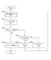
- FIG. 9is a diagram illustrating a guard ring design procedure according to the embodiment of the present technology.
- the figureshows a guard ring design procedure including a procedure for adding a dummy pad and dividing the guard ring.
- the maximum insulator junction lengthis calculated (step S910).
- the maximum insulator junction lengthis the maximum value of P.
- the guard ring widthis calculated based on the maximum insulator joining length (step S901). This can be calculated by Equation 1 described above.
- it is determined whether or not the guard ring width conforms to the design rulestep S902).
- the design ruleincludes a rule regarding application of the CMP method. As a result, when the design rule is met (step S902: Yes), the guard ring position is determined (step S903), and the design of the guard ring is finished.
- step S904it is determined whether the guard ring and the pad interfere. That is, it is determined whether or not the distance between the guard ring and the pad is appropriate. As a result, when the guard ring and the pad interfere with each other (step S904: Yes), a dummy pad is added (step S906), and the procedure from step S910 is executed again. On the other hand, when the guard ring does not interfere with the pad (step S904: No), the guard ring is divided (step S905), and the procedure from step S910 is executed again.
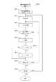
- FIG. 10is a diagram showing a maximum insulator junction length calculation procedure (step S910) in the embodiment of the present technology.
- the maximum insulator junction length (Pmax)is initialized to a value “0” (step S911).
- a side of the semiconductor chipis selected (step S912), and a pad is selected (step S913). It is determined whether there is another pad between the selected pad and the side (step S914). If there is another pad (step S914: Yes), the process returns to step S913 again, and the other pad is inserted. select.
- step S914: NoP described in FIG. 3 is calculated (step S915). The calculated P and Pmax are compared.
- step S916: YesPmax is changed to P (step S917), and the process proceeds to step S918.
- Pmaxis changed to P (step S97), and the process proceeds to step S918.
- step S916: Nothe procedure of step S917 is skipped and the process proceeds to step S918.
- step S918it is determined whether there is a next pad (step S918). That is, it is determined whether or not P has been calculated for all pads. If there is a next pad (step S918: Yes), the procedure from step S913 is executed again. On the other hand, if there is no next pad (step S918: No), it is determined whether there is a next side (step S919). That is, it is determined whether or not Pmax has been calculated for all sides. As a result, if there is a next side, the procedure from step S912 is executed again. On the other hand, if there is no next side, the maximum insulator junction length calculation procedure is terminated.
- the guard ringon the joint surface. Accordingly, the bonding strength of the semiconductor device can be set to a desired bonding strength without performing the activation process on the bonding surface.
- the processing procedure described in the above embodimentmay be regarded as a method having a series of these procedures, and a program for causing a computer to execute these series of procedures or a recording medium storing the program. You may catch it.
- a recording mediumfor example, a CD (Compact Disc), an MD (MiniDisc), a DVD (Digital Versatile Disc), a memory card, a Blu-ray disc (Blu-ray (registered trademark) Disc), or the like can be used.
- first insulating layer and the first inner layer circuit insulated by the first insulating layerare disposed outside the plurality of first pads and the plurality of first pads to be electrically connected.
- a first semiconductor chipcomprising a first bonding surface having a linear first metal layer;
- a plurality of second padsdisposed at positions opposite to the second insulating layer and the first pad and electrically connected to a second inner layer circuit insulated by the second insulating layer;
- a second semiconductor chiphaving a second bonding surface bonded to the first bonding surface, the second metal layer having a linear second metal layer disposed at a position facing the first metal layer.
- a semiconductor devicecomprising: The widths of the first metal layer and the second metal layer are set so that the width of the first insulating layer and the second insulating layer in the region from the end of the first semiconductor chip to the first pad is as follows.
- a semiconductor devicehaving a width based on a bonding strength and a bonding strength of the first metal layer and the second metal layer.
- the widths of the first metal layer and the second metal layerare determined based on the bonding strength of the first insulating layer and the second insulating layer in the region, and the first metal layer and the second metal layer.
- widths of the first metal layer and the second metal layerare substantially equal to a width Q that satisfies the following relational expression.
- zbonding strength per unit area of the first semiconductor chip and the second semiconductor chip
- xbonding strength per unit area of the first insulating layer and the second insulating layer
- ybonding strength per unit area of the first metal layer and the second metal layer
- Pthe length of the junction between the first insulating layer and the second insulating layer in a path that intersects the end of the first semiconductor chip substantially perpendicularly
- Rthe length between the first pad and the end of the first semiconductor chip in the path.
- the path described above in (3)which is a path that intersects substantially perpendicularly with an end portion of the first semiconductor chip and first reaches the first pad from the end portion of the first semiconductor chip.
- Semiconductor device.(5) The path is a path having the longest distance among paths first intersecting with the end portion of the first semiconductor chip substantially perpendicularly to the first pad from the end portion of the first semiconductor chip.
- the first bonding surfacefurther includes a first dummy pad to which the first inner layer circuit is not electrically connected
- the second bonding surfacefurther includes a second dummy pad that is disposed at a position facing the first dummy pad and is not electrically connected to the second internal circuit
- the widths of the first metal layer and the second metal layerare set such that the first insulation in a region from the end of the first semiconductor chip to the first pad or the first dummy pad first.
- the semiconductor deviceaccording to any one of (1) to (6), wherein the first metal layer and the second metal layer are divided into a predetermined number.
- the first semiconductor chip and the second semiconductor chipare configured in a rectangular shape, The widths of the first metal layer and the second metal layer are set such that the first insulating layer and the second metal layer in the region for each side of the first semiconductor chip and the second semiconductor chip, respectively.
- the semiconductor deviceaccording to any one of (1) to (7), wherein the width is based on a bonding strength of an insulating layer and a bonding strength of the first metal layer and the second metal layer.
- the first insulating layer and the first inner layer circuit insulated by the first insulating layerare arranged outside the plurality of first pads and the plurality of first pads to be electrically connected.
- a first diffusion layerhaving a semiconductor region for converting irradiated light into an electric signal by electrically connecting the first inner surface having a linear first metal layer and the first inner layer circuit.
- a first semiconductor chipcomprising: A plurality of second pads disposed at positions opposite to the second insulating layer and the first pad and electrically connected to a second inner layer circuit insulated by the second insulating layer;
- the second joint surfacethat has a linear second metal layer disposed at a position facing the first metal layer and is joined to the first joint surface and the second inner layer circuit are electrically
- An imaging devicecomprising: a second semiconductor chip comprising a second diffusion layer having a semiconductor region that is electrically connected to process the electrical signal;
- the widths of the first metal layer and the second metal layerare set so that the width of the first insulating layer and the second insulating layer in the region from the end of the first semiconductor chip to the first pad is as follows.
- An imaging devicehaving a width based on a bonding strength and a bonding strength of the first metal layer and the second metal layer.
Landscapes
- Engineering & Computer Science (AREA)
- Microelectronics & Electronic Packaging (AREA)
- Power Engineering (AREA)
- Computer Hardware Design (AREA)
- Physics & Mathematics (AREA)
- General Physics & Mathematics (AREA)
- Condensed Matter Physics & Semiconductors (AREA)
- Theoretical Computer Science (AREA)
- Evolutionary Computation (AREA)
- Geometry (AREA)
- General Engineering & Computer Science (AREA)
- Solid State Image Pick-Up Elements (AREA)
- Internal Circuitry In Semiconductor Integrated Circuit Devices (AREA)
Abstract
Description
Translated fromJapanese本技術は、半導体装置および撮像装置に関する。詳しくは、2つの半導体チップを接合して形成された半導体装置および撮像装置に関する。This technology relates to a semiconductor device and an imaging device. Specifically, the present invention relates to a semiconductor device and an imaging device formed by joining two semiconductor chips.
従来、複数の半導体チップを積層して3次元構成とし、小型化を図った半導体装置が使用されている。例えば、撮像装置において、受光素子を有する画素が2次元アレイ状に配置されて構成された半導体チップである受光素子チップと、この受光素子チップを駆動する周辺回路よりなる周辺回路チップとが、ぞれぞれの製造プロセスに基づいて個別に製造される。その後、これらを接合して積層することにより、撮像装置を構成する製造方法が採用されている。このような製造方法を採用する場合、撮像装置の信頼性を向上させるため、接合面における接合強度を高めることが望ましい。Conventionally, a semiconductor device in which a plurality of semiconductor chips are stacked to form a three-dimensional configuration and miniaturized is used. For example, in an imaging apparatus, a light receiving element chip, which is a semiconductor chip configured by arranging pixels having light receiving elements in a two-dimensional array, and a peripheral circuit chip including a peripheral circuit that drives the light receiving element chip, It is manufactured individually based on each manufacturing process. Thereafter, a manufacturing method for forming an imaging device by joining and laminating them is employed. When such a manufacturing method is employed, it is desirable to increase the bonding strength at the bonding surface in order to improve the reliability of the imaging device.
これらのチップの接合面には、半導体チップの内部の回路と電気的に接続されたパッドが配置されており、これらパッド同士が接合されることにより、チップ間における電気信号の伝達が可能になる。これらのパッドは、銅(Cu)等の金属により構成されるため、比較的高い接合強度を得ることができる。一方、接合面のパッド以外の領域には、パッド等を絶縁するための絶縁層が配置されている。この絶縁層同士の接合強度はパッド同士の接合と比較して低いことから、プラズマ処理により接合面を活性化して接合強度を向上させるシステムが提案されている(例えば、特許文献1参照。)。Pads that are electrically connected to the circuits inside the semiconductor chip are arranged on the bonding surfaces of these chips, and the electric signals can be transmitted between the chips by bonding these pads to each other. . Since these pads are made of metal such as copper (Cu), a relatively high bonding strength can be obtained. On the other hand, an insulating layer for insulating the pad or the like is disposed in a region other than the pad on the bonding surface. Since the bonding strength between the insulating layers is lower than that between the pads, a system has been proposed in which the bonding surface is activated by plasma treatment to improve the bonding strength (see, for example, Patent Document 1).
上述の従来技術は、活性化により接合面の絶縁膜同士の接合強度を向上させる効果がある一方、パッドがダメージを受けて劣化するほか、パッドを構成する銅(Cu)が飛散して半導体チップの接合装置が汚染されるという問題がある。The above prior art has the effect of improving the bonding strength between the insulating films on the bonding surface by activation, while the pad is damaged and deteriorated, and the copper (Cu) constituting the pad is scattered and the semiconductor chip. There is a problem that the joining apparatus is contaminated.
本技術はこのような状況に鑑みて生み出されたものであり、接合面の活性化処理を行うことなく半導体チップ間の接合強度を向上させることを目的とする。The present technology has been developed in view of such a situation, and an object thereof is to improve the bonding strength between semiconductor chips without performing the activation process of the bonding surface.
本技術は、上述の問題点を解消するためになされたものであり、その第1の側面は、第1の絶縁層と上記第1の絶縁層により絶縁される第1の内層回路が電気的に接続される複数の第1のパッドと上記複数の第1のパッドの外側に配置される線状の第1の金属層とを有する第1の接合面を備える第1の半導体チップと、第2の絶縁層と上記第1のパッドに対向する位置に配置されるとともに上記第2の絶縁層により絶縁される第2の内層回路が電気的に接続される複数の第2のパッドと上記第1の金属層に対向する位置に配置される線状の第2の金属層とを有して上記第1の接合面と接合される第2の接合面を備える第2の半導体チップとを具備する半導体装置であって、上記第1の金属層および上記第2の金属層の幅は、上記第1の半導体チップの端部から上記第1のパッドに至る領域の上記第1の絶縁層および上記第2の絶縁層の接合強度と上記第1の金属層および上記第2の金属層の接合強度とに基づく幅である半導体装置である。これにより、上記第1の半導体チップの端部から上記第1のパッドに至る領域の上記第1の絶縁層および上記第2の絶縁層の接合強度と上記第1の金属層および上記第2の金属層の接合強度とに基づく幅の上記第1の金属層および上記第2の金属層が配置されるという作用をもたらす。The present technology has been made to solve the above-described problems, and the first aspect thereof is that the first inner layer circuit insulated by the first insulating layer and the first insulating layer is electrically connected. A first semiconductor chip comprising a first bonding surface having a plurality of first pads connected to the first pad and a linear first metal layer disposed outside the plurality of first pads; A plurality of second pads, which are arranged at positions opposite to the two insulating layers and the first pad, and are electrically connected to a second inner layer circuit insulated by the second insulating layer; And a second semiconductor chip having a second joining surface joined to the first joining surface, and having a linear second metal layer disposed at a position facing the first metal layer. The width of the first metal layer and the second metal layer is the first semiconductor layer. Based on the bonding strength of the first insulating layer and the second insulating layer in the region from the end of the chip to the first pad and the bonding strength of the first metal layer and the second metal layer. It is a semiconductor device having a width. Thereby, the bonding strength of the first insulating layer and the second insulating layer in the region from the end of the first semiconductor chip to the first pad, the first metal layer, and the second The first metal layer and the second metal layer having a width based on the bonding strength of the metal layer are provided.
また、この第1の側面において、上記第1の金属層および上記第2の金属層の幅は、上記領域における上記第1の絶縁層および上記第2の絶縁層の接合強度と上記第1の金属層および上記第2の金属層の接合強度との平均値に基づく幅であってもよい。これにより、上記領域における上記第1の絶縁層および上記第2の絶縁層の接合強度と上記第1の金属層および上記第2の金属層の接合強度との平均値に基づく幅の上記第1の金属層および上記第2の金属層が配置されるという作用をもたらす。Further, in the first aspect, the widths of the first metal layer and the second metal layer are determined by the bonding strength of the first insulating layer and the second insulating layer in the region and the first metal layer. The width may be based on an average value of the bonding strength of the metal layer and the second metal layer. Thereby, the first width having a width based on an average value of the bonding strength of the first insulating layer and the second insulating layer and the bonding strength of the first metal layer and the second metal layer in the region. The metal layer and the second metal layer are arranged.
また、この第1の側面において、上記第1の金属層および上記第2の金属層の幅は、以下の関係式を満たす幅Qに略等しい幅であってもよい。
(x×P+y×Q)/R>z
ただし、
z:上記第1の半導体チップおよび上記第2の半導体チップの単位面積当たりの接合強度、
x:上記第1の絶縁層および上記第2の絶縁層の単位面積当たりの接合強度、
y:上記第1の金属層および上記第2の金属層の単位面積当たりの接合強度、
P:上記第1の半導体チップの端部と略垂直に交わる経路における上記第1の絶縁層および上記第2の絶縁層の接合部分の長さ、
R:上記経路における上記第1のパッドと上記第1の半導体チップの端部との間の長さ
である。これにより、上記第1の半導体チップの端部と略垂直に交わる経路における上記第1の絶縁層および上記第2の絶縁層の接合部分の長さ等に基づく幅の上記第1の金属層および上記第2の金属層が配置されるという作用をもたらす。In the first aspect, the widths of the first metal layer and the second metal layer may be substantially equal to a width Q that satisfies the following relational expression.
(X × P + y × Q) / R> z
However,
z: bonding strength per unit area of the first semiconductor chip and the second semiconductor chip;
x: bonding strength per unit area of the first insulating layer and the second insulating layer;
y: bonding strength per unit area of the first metal layer and the second metal layer,
P: the length of the junction between the first insulating layer and the second insulating layer in a path that intersects the end of the first semiconductor chip substantially perpendicularly;
R: the length between the first pad and the end of the first semiconductor chip in the path. As a result, the first metal layer having a width based on the length or the like of the joining portion of the first insulating layer and the second insulating layer in a path substantially perpendicular to the end of the first semiconductor chip, and The second metal layer is arranged.
また、この第1の側面において、上記経路は、上記第1の半導体チップの端部と略垂直に交わって上記第1の半導体チップの端部から最初に上記第1のパッドに至る経路であってもよい。これにより、上記第1の半導体チップの端部と上記第1のパッドとの間の最短の上記経路における上記第1の絶縁層および上記第2の絶縁層の接合部分の長さ等に基づく幅の上記第1の金属層および上記第2の金属層が配置されるという作用をもたらす。In the first aspect, the path is a path that intersects the end of the first semiconductor chip substantially perpendicularly and first reaches the first pad from the end of the first semiconductor chip. May be. Thereby, the width based on the length of the joint portion of the first insulating layer and the second insulating layer in the shortest path between the end of the first semiconductor chip and the first pad, etc. The first metal layer and the second metal layer are disposed.
また、この第1の側面において、上記経路は、上記第1の半導体チップの端部と略垂直に交わって上記第1の半導体チップの端部から最初に上記第1のパッドに至る経路のうち最も距離が長い経路であってもよい。これにより、最も接合強度が小さい上記経路における上記第1の絶縁層および上記第2の絶縁層の接合部分の長さ等に基づく幅の上記第1の金属層および上記第2の金属層が配置されるという作用をもたらす。In the first aspect, the path includes a path that intersects the end of the first semiconductor chip substantially perpendicularly and first reaches the first pad from the end of the first semiconductor chip. The route with the longest distance may be used. Thereby, the first metal layer and the second metal layer having a width based on the length of the joint portion of the first insulating layer and the second insulating layer in the path having the smallest bonding strength are arranged. It brings about the effect of being.
また、この第1の側面において、上記第1の接合面は、上記第1の内層回路が電気的に接続されない第1のダミーパッドをさらに有し、上記第2の接合面は、上記第1のダミーパッドと対向する位置に配置されるとともに上記第2の内装回路と電気的に接続されない第2のダミーパッドをさらに有し、上記第1の金属層および上記第2の金属層の幅は、上記第1の半導体チップの端部から最初に上記第1のパッドまたは上記第1のダミーパッドに至る領域の上記第1の絶縁層および上記第2の絶縁層の接合強度と上記第1の金属層および上記第2の金属層の接合強度とに基づく幅であってもよい。これにより、上記第1の半導体チップの端部から最初に上記第1のパッドまたは上記第1のダミーパッドに至る領域の上記第1の絶縁層および上記第2の絶縁層の接合強度と上記第1の金属層および上記第2の金属層の接合強度とに基づく幅の上記第1の金属層および上記第2の金属層が配置されるという作用をもたらす。In the first aspect, the first bonding surface further includes a first dummy pad to which the first inner layer circuit is not electrically connected, and the second bonding surface is the first bonding surface. And a second dummy pad that is not electrically connected to the second interior circuit, and the widths of the first metal layer and the second metal layer are as follows: The bonding strength of the first insulating layer and the second insulating layer in the region from the end of the first semiconductor chip to the first pad or the first dummy pad first and the first The width may be based on the bonding strength of the metal layer and the second metal layer. Accordingly, the bonding strength between the first insulating layer and the second insulating layer in the region from the end of the first semiconductor chip to the first pad or the first dummy pad first, and the first The first metal layer and the second metal layer having a width based on the bonding strength of one metal layer and the second metal layer are provided.
また、この第1の側面において、上記第1の金属層および上記第2の金属層は、所定の個数に分割されてもよい。これにより、上記第1の金属層および上記第2の金属層が分割されるという作用をもたらす。Further, in the first aspect, the first metal layer and the second metal layer may be divided into a predetermined number. This brings about the effect | action that the said 1st metal layer and said 2nd metal layer are divided | segmented.
また、この第1の側面において、上記第1の半導体チップおよび上記第2の半導体チップは、矩形形状に構成され、上記第1の金属層および上記第2の金属層の幅は、上記第1の半導体チップおよび上記第2の半導体チップのそれぞれの辺毎の上記領域における上記第1の絶縁層および上記第2の絶縁層の接合強度と上記第1の金属層および上記第2の金属層の接合強度とに基づく幅であってもよい。これにより、半導体チップのそれぞれの辺毎の上記領域における上記第1の絶縁層および上記第2の絶縁層の接合強度と上記第1の金属層および上記第2の金属層の接合強度とに基づく幅の上記第1の金属層および上記第2の金属層が配置されるという作用をもたらす。In the first aspect, the first semiconductor chip and the second semiconductor chip are formed in a rectangular shape, and the widths of the first metal layer and the second metal layer are set to the first side. The bonding strength of the first insulating layer and the second insulating layer in the region for each side of the semiconductor chip and the second semiconductor chip, and the first metal layer and the second metal layer The width may be based on the bonding strength. Thereby, based on the bonding strength of the first insulating layer and the second insulating layer and the bonding strength of the first metal layer and the second metal layer in the region for each side of the semiconductor chip. The first metal layer and the second metal layer having a width are provided.
また、本技術の第2の側面は、第1の絶縁層と上記第1の絶縁層により絶縁される第1の内層回路が電気的に接続される複数の第1のパッドと上記複数の第1のパッドの外側に配置される線状の第1の金属層とを有する第1の接合面および上記第1の内層回路が電気的に接続されて照射された光を電気信号に変換する半導体領域を有する第1の拡散層を備える第1の半導体チップと、第2の絶縁層と上記第1のパッドに対向する位置に配置されるとともに上記第2の絶縁層により絶縁される第2の内層回路が電気的に接続される複数の第2のパッドと上記第1の金属層に対向する位置に配置される線状の第2の金属層とを有して上記第1の接合面と接合される第2の接合面および上記第2の内層回路が電気的に接続されて上記電気信号を処理する半導体領域を有する第2の拡散層を備える第2の半導体チップとを具備する撮像装置であって、上記第1の金属層および上記第2の金属層の幅は、上記第1の半導体チップの端部から上記第1のパッドに至る領域の上記第1の絶縁層および上記第2の絶縁層の接合強度と上記第1の金属層および上記第2の金属層の接合強度とに基づく幅である撮像装置である。これにより、上記第1の半導体チップの端部から上記第1のパッドに至る領域の上記第1の絶縁層および上記第2の絶縁層の接合強度と上記第1の金属層および上記第2の金属層の接合強度とに基づく幅の上記第1の金属層および上記第2の金属層が配置されるという作用をもたらす。The second aspect of the present technology provides a plurality of first pads to which the first inner layer circuit electrically insulated by the first insulating layer and the first insulating layer is electrically connected, and the plurality of first pads. Semiconductor that converts irradiated light into an electrical signal by electrically connecting a first bonding surface having a linear first metal layer disposed outside one pad and the first inner layer circuit. A first semiconductor chip having a first diffusion layer having a region; a second semiconductor chip disposed at a position opposite to the second insulating layer and the first pad; and insulated by the second insulating layer A plurality of second pads to which an inner layer circuit is electrically connected and a linear second metal layer disposed at a position facing the first metal layer; The second joint surface to be joined and the second inner layer circuit are electrically connected to process the electrical signal. And a second semiconductor chip having a second diffusion layer having a semiconductor region to be processed, wherein the width of the first metal layer and the second metal layer is the first semiconductor chip Width based on the bonding strength of the first insulating layer and the second insulating layer and the bonding strength of the first metal layer and the second metal layer in the region from the end of the first pad to the first pad It is an imaging device. Thereby, the bonding strength of the first insulating layer and the second insulating layer in the region from the end of the first semiconductor chip to the first pad, the first metal layer, and the second The first metal layer and the second metal layer having a width based on the bonding strength of the metal layer are provided.
本技術によれば、接合面の活性化処理を行うことなく半導体チップ間の接合強度を向上させるという優れた効果を奏し得る。なお、ここに記載された効果は必ずしも限定されるものではなく、本開示中に記載されたいずれかの効果であってもよい。According to the present technology, an excellent effect of improving the bonding strength between the semiconductor chips without performing the activation process of the bonding surface can be achieved. Note that the effects described here are not necessarily limited, and may be any of the effects described in the present disclosure.
以下、本技術を実施するための形態(以下、実施の形態と称する)について説明する。説明は以下の順序により行う。
1.第1の実施の形態(ガードリングを使用する場合の例)
2.第2の実施の形態(ガードリングを分割する場合の例)
3.第3の実施の形態(ダミーパッドを使用する場合の例)Hereinafter, modes for carrying out the present technology (hereinafter referred to as embodiments) will be described. The description will be made in the following order.
1. 1st Embodiment (example in the case of using a guard ring)
2. Second embodiment (an example of dividing a guard ring)
3. Third embodiment (example of using dummy pad)
<1.第1の実施の形態>
[半導体装置の構成]
図1は、本技術の第1の実施の形態における半導体装置10の構成例を示す図である。同図は、カメラ等に使用する撮像装置の構成を表した断面図である。この撮像装置を例に挙げて、本技術の実施の形態における半導体装置10の構成を説明する。この半導体装置10は、第1の半導体チップ100と、第2の半導体チップ200とを備える。また、半導体装置10は、第1の半導体チップ100および第2の半導体チップ200が同図に記載した「B」の位置において接合されて構成される。なお、半導体装置10は、請求の範囲に記載の撮像装置の一例である。<1. First Embodiment>
[Configuration of semiconductor device]
FIG. 1 is a diagram illustrating a configuration example of the
第1の半導体チップ100は、画像を電気信号に変換するものである。この第1の半導体チップ100には、照射された光に応じた電気信号を生成する画素(不図示)が2次元アレイ状に配置される。これらの画素により生成された電気信号は、第2の半導体チップ200に対して出力される。この第1の半導体チップ100は、マイクロレンズ101と、カラーフィルタ102と、第1の拡散層110と、配線層131と、ビア132と、第1の絶縁層129と、第1のパッド124と、第1のガードリング121とを備える。The
マイクロレンズ101は、上述の画素に光学画像を結像するものである。カラーフィルタ102は、所望の波長の光を画素に入射させるための光学的なフィルタである。The
第1の拡散層110は、上述の画素が生成された半導体領域である。この画素には、マイクロレンズ101およびカラーフィルタ102がそれぞれ配置される。The
配線層131は、電気信号を伝達するものである。この配線層131は、XYマトリクス状に配置されて、第1の拡散層110に形成された複数の画素のそれぞれに配線される。この配線層131を経由して、画素に対する電源の供給、制御信号の入力、電気信号の出力が行われる。配線層131は、複数の層状に積層することができる。同図においては、3層に積層された配線層131の例を表した。ビア132は、異なる層に配置された配線層131を電気的に接続するものである。これら、配線層131およびビア132には、例えば、銅(Cu)を使用することができる。なお、配線層131およびビア132は、第1の内層回路を構成する。The
第1の絶縁層129は、配線層131およびビア132を絶縁するものである。この第1の絶縁層129は、後述する第2の絶縁層229と接合される。第1の絶縁層129には、例えば、二酸化ケイ素(SiO2[0])や有機シリカガラスを使用することができる。The first insulating
第1のパッド124は、配線層131およびビア132と電気的に接続されて、電気信号を第2の半導体チップ200との間で相互に伝達するものである。伝達する信号に応じた個数の第1のパッドを第1の半導体チップ100に配置することができる。また、第1のパッド124は、後述する第2のパッド224と接合される。この第1のパッド124には、例えば、銅(Cu)を使用することができる。The
第1のガードリング121は、第1のパッドの外側に配置される線状の金属の層である。また、第1のガードリング121は、後述する第2のガードリング221と接合される。この第1のガードリング121は、配線層131およびビア132と電気的に接続されて、例えば、接地線に接続することができる。また、この第1のガードリング121を配線層131およびビア132とは接続せず、電気的に独立した構成にしてもよい。この第1のガードリング121には、例えば、銅(Cu)を使用することができる。なお、第1のガードリング121は、請求の範囲に記載の第1の金属層の一例である。The
第2の半導体チップ200は、第1の半導体チップ100と電気的および機械的に接合されて第1の半導体チップ100の画素に対する制御信号の生成および画素により生成された電気信号の処理等を行うものである。この処理としては、例えば、第1の半導体チップ100により生成されたアナログの電気信号をデジタルの電気信号に変換するアナログデジタル変換が該当する。この第2の半導体チップ200は、第2の拡散層210と、配線層231と、ビア232と、第2の絶縁層229と、第2のパッド224と、第2のガードリング221とを備える。The
第2の拡散層210は、上述の制御信号の生成および電気信号の処理等を行う半導体領域である。この半導体領域により処理された電気信号は、画像信号として半導体装置10の外部に出力される。The
配線層231は、電気信号を伝達するものである。配線層131と同様に、この配線層231は、複数の層状に積層することができる。同図においては、4層に積層された配線層231の例を表した。ビア232は、異なる層に配置された配線層231を電気的に接続するものである。これら、配線層231およびビア232には、例えば、銅(Cu)を使用することができる。なお、配線層231およびビア232は、第2の内層回路を構成する。The
第2の絶縁層229は、配線層231およびビア232を絶縁するものである。前述のように、この第2の絶縁層229は、第1の絶縁層129と接合される。第2の絶縁層229には、例えば、二酸化ケイ素(SiO2[0])や有機シリカガラスを使用することができる。The second
第2のパッド224は、配線層231およびビア232と電気的に接続されて、電気信号を第1の半導体チップ100との間で相互に伝達するものである。前述のように、この第2のパッド224は、第1のパッド124と接合される。この第1のパッド224には、例えば、銅(Cu)を使用することができる。The
第2のガードリング221は、第2のパッドの外側に配置される線状の金属の層である。前述のように、第2のガードリング221は、第1のガードリング121と接合される。この第2のガードリング221には、例えば、銅(Cu)を使用することができる。なお、第2のガードリング221は、請求の範囲に記載の第2の金属層の一例である。The
[半導体チップの構成]
図2は、本技術の第1の実施の形態における半導体チップの構成例を示す図である。同図は、接合される前の第1の半導体チップ100および第2の半導体チップ200の構成を表したものである。同図におけるaは第2の半導体チップ200における接合面120(同図におけるaの点線で示される面)の構成を表し、同図におけるbは第2の半導体チップ200における接合面220(同図におけるbの点線で示される面)を表している。何れの半導体チップも矩形形状の接合面を有している。[Configuration of semiconductor chip]
FIG. 2 is a diagram illustrating a configuration example of the semiconductor chip according to the first embodiment of the present technology. The figure shows the configuration of the
接合面120には、第1の絶縁層129と、第1のパッド124と、第1のガードリング121とが配置されている。The first insulating
第1のパッド124は、第1の絶縁層129に埋め込まれた島状に配置される。また、第1のガードリング121は、接合面120を縁取りする形状に配置される。The
接合面220には、第2の絶縁層229と、第2のパッド224と、第2のガードリング221とが配置される。The second
第2のパッド224は、第2の絶縁層229に埋め込まれた島状に配置される。また、第2のパッド224は、第1のパッド124と対称な位置に配置される。第2のガードリング221は、接合面220を縁取りする形状に配置される。The
これら第1の接合面120および第2の接合面220が接合される。この際、第1のパッド124および第2のパッド224、第1の絶縁層129および第2の絶縁層229ならびに第1のガードリング121および第2のガードリング221がそれぞれ接合される。接合方法については、後述する。The first
通常、第1のパッド124および第2のパッド224のような金属同士の結合強度は、比較的高い。一方、接合面の大部分を占める第1の絶縁層129および第2の絶縁層229の間の接合強度は、比較的低い。活性化処理を行った場合には、絶縁層同士の接合強度を向上させることができるが、前述のような問題が発生する。そこで、第1のガードリング121および第2のガードリング221を接合面に配置し、接合面に占める金属同士の接合部を増やすことにより、所望の接合強度を得ることができる。また、第1のガードリング121および第2のガードリング221をそれぞれ接合面120および220の端部を縁取りする形状に配置することにより、接合面の端部におけるクラックの発生を防止する効果がある。通常、接合面の端部は、応力が集中するため、クラックを生じ易い。そこで、この部分にガードリング221等を配置して接合強度を向上させることにより、クラックの発生を防止することができる。Usually, the bonding strength between metals such as the
[ガードリングの幅]
図3は、本技術の第1の実施の形態におけるガードリングの幅を示す図である。同図は、第1のガードリング121および第2のガードリング221の幅の算出方法を表したものである。同図におけるaは第1の半導体チップ100の端部の正面図を表し、同図におけるbは半導体装置10の接合部の断面図を表している。[Width of guard ring]
FIG. 3 is a diagram illustrating the width of the guard ring according to the first embodiment of the present technology. This figure shows a method for calculating the widths of the
前述のように、第1のパッド124および第2のパッド224のような金属同士の接合強度と比べて、絶縁層同士の接合強度は低い。通常、第1のパッド124等は、応力が集中する第1の半導体チップ100等の周縁部から離れた領域に配置される。このため、ガードリング121等を第1の半導体チップ100等の周縁部に配置して接合強度の不足を補うことができる。ここで、第1のガードリング121および第2のガードリング221の幅をQにより表す。このQは、第1の半導体チップ100の端部から第1のパッド124に至る領域の第1の絶縁層129および第2の絶縁層229の接合強度と第1のガードリング121および第2のガードリング221の接合強度とに基づいて算出することができる。As described above, the bonding strength between the insulating layers is lower than the bonding strength between the metals such as the
同図におけるaの「C」を付した第1のパッド124を例に挙げて説明すると、第1の半導体チップ100の端部から第1のパッド124までの領域の絶縁層同士の接合強度とガードリング同士の接合強度に基づいてQを算出することができる。ここで、この領域における絶縁層同士の接合部分の長さをPにより表す。第1の半導体チップ100および第2の半導体チップ200において所望の接合強度を得るためには、上記領域における絶縁層部分の接合強度とガードリング部分の接合強度との平均の接合強度をこの所望の接合強度を超える値にする必要がある。ここで、第1の半導体チップ100および第2の半導体チップ200の所望の接合強度とは、半導体装置10に要求される信頼性等を考慮して設定される接合強度であり、これら半導体チップの単位面積当たりの接合強度により表される値である。The
これをzにより表すと、zとPおよびQとの関係は次式のようになる。
(x×P+y×Q)/R>z ・・・式1
ただし、xは、第1の絶縁層129および第2の絶縁層229の単位面積当たりの接合強度を表す。yは、第1のガードリングおよび第2のガードリングの単位面積当たりの接合強度を表す。Rは、第1のパッド124と第1の半導体チップ100の端部との間の長さを表す。なお、同図においては、RはPおよびQの合計と等しい長さになる。式1の左辺は、上記領域における単位長さ(同図におけるaの縦方向の単位長さ)当たりの接合強度の合計値をRで除算して当該領域の接合強度の平均値を算出する演算を表している。When this is expressed by z, the relationship between z and P and Q is as follows.
(X × P + y × Q) / R> z Equation 1
Note that x represents the bonding strength per unit area of the first insulating
図2において説明したように、第1の半導体チップ100および第2の半導体チップ200の接合面は矩形形状であるため、Qの算出は、4辺について行う。なお、Qの値は、辺毎に異なる値を採用することができる。また、全ての辺について算出したQのうち最大のものを4辺共通のQの値にすることもできる。As described with reference to FIG. 2, since the bonding surfaces of the
なお、同図におけるaに表したように、上述のPには、第1の半導体チップ100の端部と略垂直に交わる経路における第1の絶縁層129および第2の絶縁層229の接合部分の長さを用いることができる。また、当該経路中に第1のパッド124が間に入らない経路を選択することも可能である。例えば、同図におけるaの「D」を付した第1のパッド124は、第1の半導体チップ100の端部までの経路に「E」を付した第1のパッド124が入っているため、この経路に係るP'は接合強度の算出から除外する。このような場合には、「E」を付した第1のパッド124により、Qの算出が行われる。これにより、Qの算出をより正確に行うことができる。Note that, as shown in a in FIG. 6, the above-described P is a joint portion of the first insulating
また、上述した第1のパッド124が間に入らない経路のうち、最長の経路に基づいてQを算出すると好適である。Pの部分が最も長い部分は絶縁層同士の接合部分が最も長い部分に該当する。このため、最も接合強度が小さい部分を基準としてQを算出することとなり、Qの算出精度をさらに向上させることが可能なためである。In addition, it is preferable to calculate Q based on the longest path among the paths where the
[アライメント時のずれ等を考慮する場合]
図4は、本技術の第1の実施の形態におけるアライメント時のずれ等を示す図である。同図におけるaは、第1の半導体チップ100および第2の半導体チップ200を接合する際にアライメントずれe1を生じた場合の例を表したものである。このような場合には、第1のガードリング121および第2のガードリング221の接合部分の長さが減少する。このため、e1をQに加えて第1のガードリング121および第2のガードリング221を製造する必要がある。[When considering misalignment during alignment]
FIG. 4 is a diagram illustrating a shift or the like at the time of alignment in the first embodiment of the present technology. In the figure, a represents an example in the case where an alignment deviation e1 occurs when the
また、同図におけるbは、ウェハから半導体装置10を切り出す際のダイシングのずれe2を生じた場合の例を表したものである。ここで、同図におけるbの401は、ダイシング位置を表す。このような場合にも、第1のガードリング121および第2のガードリング221の接合部分の減少を防ぐため、e2をQに加える必要がある。Further, b in the figure represents an example in the case where a dicing deviation e2 occurs when the
[半導体装置の製造方法]
半導体装置10は、以下の手順により製造することができる。前述のように算出された幅Qの第1のガードリング121および第2のガードリング221を備えた第1の半導体チップ100および第2の半導体チップ200を製造する。これらは、一般的な半導体チップの製造方法により製造することができる。また、第1のガードリング121および第2のガードリング221は、第1のパッド124および第2のパッド224と同一の製法により製造することができる。次に、第1の半導体チップ100の第1の接合面120および第2の半導体チップ200の接合面220を研磨して、これらの接合面を平滑にする。この研磨にはCMP(Chemical Mechanical Polishing)法を使用することができる。次に、第1の半導体チップ100および第2の半導体チップ200のアライメントを行い、接合面同士の貼合せを行う。貼り合せた状態で300から600℃の温度に加熱し、両者を接合させる。これにより、半導体装置10を製造することができる。[Method for Manufacturing Semiconductor Device]
The
このように、本技術の第1の実施の形態では、半導体チップのそれぞれの接合面に第1のガードリング121および第2のガードリング221を設ける。これらのガードリングとして、第1の半導体チップ100の端部から第1のパッド124に至る領域の絶縁層同士の接合部分の強度とガードリング同士の接合部分の強度とに基づいて算出された幅のガードリングを使用する。これにより、半導体装置10の接合強度を所望の接合強度にすることができる。As described above, in the first embodiment of the present technology, the
[第1の変形例]
上述の実施の形態では、第1のガードリング121および第2のガードリング221は、同一の幅にしていた。これに対し、第1のガードリング121および第2のガードリング221の幅を異なる値にすることもできる。アライメントずれ等の製造時の誤差を吸収するためである。[First Modification]
In the above-described embodiment, the
図5は、本技術の第1の実施の形態の変形例におけるガードリングの幅を示す図である。同図は、第1のガードリング121および第2のガードリング221の幅が異なる場合の例を表した図である。この場合においても、第1のガードリング121および第2のガードリング221の接合部分の長さをQに等しくすることにより、所望の接合強度を得ることができる。FIG. 5 is a diagram illustrating the width of the guard ring in the modification of the first embodiment of the present technology. This figure shows an example in which the widths of the
<2.第2の実施の形態>
上述の実施の形態では、半導体チップにはそれぞれ1つのガードリングを使用していた。これに対し、本技術の第2の実施の形態では、ガードリングを分割し、複数のガードリングを使用する。これにより、CMP研磨時の不具合の発生を防止する。<2. Second Embodiment>
In the above-described embodiment, one guard ring is used for each semiconductor chip. On the other hand, in the second embodiment of the present technology, the guard ring is divided and a plurality of guard rings are used. This prevents the occurrence of defects during CMP polishing.
[ガードリングの構成]
図6は、本技術の第2の実施の形態におけるガードリングを示す図である。前述のように、半導体装置10の製造工程において、CMP法による半導体チップの接合面の研磨が行われる。この際、第1のガードリング121および第2のガードリング221の幅Qが大きすぎると、ガードリング部分が過剰に削られる、いわゆるディッシングが生じる場合がある。これを防ぐため、同図に表したように第1のガードリング121および第2のガードリング221を分割して配置する。同図は、それぞれ4つに分割した例を表したものである。この際、分割されたガードリングの幅の合計をQに等しくする。これ以外の半導体装置10の構成は図1において説明した半導体装置10と同様であるため、説明を省略する。[Configuration of guard ring]
FIG. 6 is a diagram illustrating a guard ring according to the second embodiment of the present technology. As described above, in the manufacturing process of the
このように、本技術の第2の実施の形態によれば、ガードリングを分割することにより、所望の接合強度保ちながら、CMP研磨時のディッシングの発生を防止することができる。As described above, according to the second embodiment of the present technology, by dividing the guard ring, it is possible to prevent dishing during CMP polishing while maintaining a desired bonding strength.
<3.第3の実施の形態>
上述の実施の形態では、第1の半導体チップ100の端部から第1のパッド124に至る領域の絶縁層同士の接合部分の強度等に基づいてQを算出していた。これに対し、本技術の第3の実施の形態では、接合面にダミーパッドを追加して第1の半導体チップ100の端部から第1のパッド124またはダミーパッドに至る領域に変更し、Qを算出する。これにより、接合強度を保ちながらQを小さくすることができる。<3. Third Embodiment>
In the above-described embodiment, Q is calculated based on the strength of the bonding portion between the insulating layers in the region from the end of the
[半導体装置の構成]
図7は、本技術の第3の実施の形態における半導体装置10の構成例を示す図である。同図の半導体装置10は、第1のダミーパッド125および第2のダミーパッド225がそれぞれ第1の半導体チップ100および第2の半導体チップ200に配置されている点で、図1において説明した半導体装置10と異なっている。[Configuration of semiconductor device]
FIG. 7 is a diagram illustrating a configuration example of the
[ダミーパッドの構成]
図8は、本技術の第3の実施の形態におけるダミーパッドを示す図である。本技術の第1の実施の形態では、第1の半導体チップ100の端部から第1のパッド124に至る領域の絶縁物同士の接合強度等に基づいてQを算出していた。しかし、同図における上側の図に表したように、第1のパッド124と第1の半導体チップ100の端部との距離が大きい場合、Qの値も大きなものとなる。このため、第1のガードリング121が他の第1のパッドと接近し、デザインルール違反となる場合が生じる。そこで、同図における下側の図に表したように、第1のパッド124と第1の半導体チップ100の端部との間に第1のダミーパッド125を配置する。この第1のダミーパッド125は、接合面120に配置されるものの、配線層131およびビア132とは接続されておらず、電気的に独立したパッドである。[Dummy pad configuration]
FIG. 8 is a diagram illustrating a dummy pad according to the third embodiment of the present technology. In the first embodiment of the present technology, Q is calculated based on the bonding strength or the like of the insulators in the region from the end of the
なお、接合面220には、この第1のダミーパッド125と対向する位置にダミーパッド225が配置される。また、Qは、第1の半導体チップ100の端部から最初に第1のパッド124または第1のダミーパッド125に至る領域の絶縁層同士の接合強度とガードリング同士の接合強度とに基づいて算出される。第1のダミーパッド125および第2のダミーパッド225を追加することにより、Pを短くすることができ、これに基づくQも短くすることができる。これにより、デザインルール違反を回避することができる。これ以外の半導体装置10の構成は図1において説明した半導体装置10と同様であるため、説明を省略する。Note that a
[ガードリングの設計手順]
図9は、本技術の実施の形態におけるガードリングの設計手順を示す図である。同図は、ダミーパッドの追加およびガードリングの分割の手順を含むガードリングの設計手順を表したものである。まず、最大絶縁物接合長を算出する(ステップS910)。ここで、最大絶縁物接合長とは、Pの最大値である。次に、最大絶縁物接合長に基づいてガードリング幅を算出する(ステップS901)。これは、前述の式1により算出することができる。次に、ガードリングの幅がデザインルールに適合するか否かを判断する(ステップS902)。ここで、デザインルールには、CMP法の適用に関するルールが含まれている。その結果、デザインルールに適合する場合には(ステップS902:Yes)、ガードリング位置を決定し(ステップS903)、ガードリングの設計を終了する。[Guard ring design procedure]
FIG. 9 is a diagram illustrating a guard ring design procedure according to the embodiment of the present technology. The figure shows a guard ring design procedure including a procedure for adding a dummy pad and dividing the guard ring. First, the maximum insulator junction length is calculated (step S910). Here, the maximum insulator junction length is the maximum value of P. Next, the guard ring width is calculated based on the maximum insulator joining length (step S901). This can be calculated by Equation 1 described above. Next, it is determined whether or not the guard ring width conforms to the design rule (step S902). Here, the design rule includes a rule regarding application of the CMP method. As a result, when the design rule is met (step S902: Yes), the guard ring position is determined (step S903), and the design of the guard ring is finished.
一方、デザインルールに適合しない場合には(ステップS902:No)、ガードリングとパッドとが干渉するか否かを判断する(ステップS904)。すなわち、ガードリングとパッドとの距離が適切か否かを判断する。その結果、ガードリングとパッドとが干渉する場合には(ステップS904:Yes)、ダミーパッドを追加し(ステップS906)、再度ステップS910からの手順を実行する。一方、ガードリングとパッドとが干渉しない場合には(ステップS904:No)、ガードリングを分割し(ステップS905)、再度ステップS910からの手順を実行する。On the other hand, if the design rule is not met (step S902: No), it is determined whether the guard ring and the pad interfere (step S904). That is, it is determined whether or not the distance between the guard ring and the pad is appropriate. As a result, when the guard ring and the pad interfere with each other (step S904: Yes), a dummy pad is added (step S906), and the procedure from step S910 is executed again. On the other hand, when the guard ring does not interfere with the pad (step S904: No), the guard ring is divided (step S905), and the procedure from step S910 is executed again.
図10は、本技術の実施の形態における最大絶縁物接合長算出手順(ステップS910)を示す図である。まず、最大絶縁物接合長(Pmax)を値「0」に初期化する(ステップS911)。次に、半導体チップの辺を選択し(ステップS912)、パッドを選択する(ステップS913)。選択したパッドと辺との間に他のパッドがあるか否かを判断し(ステップS914)、他のパッドがある場合には(ステップS914:Yes)、再度ステップS913に戻り、他のパッドを選択する。一方、他のパッドがない場合には(ステップS914:No)、図3において説明したPを算出する(ステップS915)。算出したPとPmaxとを比較し、PmaxよりPの方が大きい場合には(ステップS916:Yes)、PmaxをPに変更し(ステップS917)、ステップS918の手順に移行する。一方、PがPmax以下の場合には(ステップS916:No)、ステップS917の手順をスキップしてステップS918の手順に移行する。FIG. 10 is a diagram showing a maximum insulator junction length calculation procedure (step S910) in the embodiment of the present technology. First, the maximum insulator junction length (Pmax) is initialized to a value “0” (step S911). Next, a side of the semiconductor chip is selected (step S912), and a pad is selected (step S913). It is determined whether there is another pad between the selected pad and the side (step S914). If there is another pad (step S914: Yes), the process returns to step S913 again, and the other pad is inserted. select. On the other hand, when there is no other pad (step S914: No), P described in FIG. 3 is calculated (step S915). The calculated P and Pmax are compared. If P is larger than Pmax (step S916: Yes), Pmax is changed to P (step S917), and the process proceeds to step S918. On the other hand, when P is less than or equal to Pmax (step S916: No), the procedure of step S917 is skipped and the process proceeds to step S918.
ステップS918において、次のパッドがあるか否かを判断する(ステップS918)。すなわち、全てのパッドについてPの算出を行ったか否かを判断する。次のパッドがある場合には、(ステップS918:Yes)、再度ステップS913からの手順を実行する。一方、次のパッドがない場合には(ステップS918:No)、次の辺があるか否かを判断する(ステップS919)。すなわち、全ての辺についてPmaxの算出を行ったか否かを判断する。その結果、次の辺がある場合には、再度ステップS912からの手順を実行する。一方、次の辺がない場合には、最大絶縁物接合長算出手順を終了する。In step S918, it is determined whether there is a next pad (step S918). That is, it is determined whether or not P has been calculated for all pads. If there is a next pad (step S918: Yes), the procedure from step S913 is executed again. On the other hand, if there is no next pad (step S918: No), it is determined whether there is a next side (step S919). That is, it is determined whether or not Pmax has been calculated for all sides. As a result, if there is a next side, the procedure from step S912 is executed again. On the other hand, if there is no next side, the maximum insulator junction length calculation procedure is terminated.
このように、本技術の第3の実施の形態によれば、ダミーパッドを追加することにより、所望の接合強度を保ちながら、デザインルール違反を回避することができる。Thus, according to the third embodiment of the present technology, by adding a dummy pad, it is possible to avoid a design rule violation while maintaining a desired bonding strength.
上述のように、本技術の実施の形態では、半導体チップの端部からパッドに至る領域における絶縁層同士の接合部分の強度とガードリング同士の接合部分の強度とに基づいて算出された幅のガードリングを接合面に配置して使用する。これにより、接合面の活性化処理を行うことなく、半導体装置の接合強度を所望の接合強度にすることができる。As described above, in the embodiment of the present technology, the width calculated based on the strength of the bonding portion between the insulating layers and the strength of the bonding portion between the guard rings in the region from the end of the semiconductor chip to the pad. Use the guard ring on the joint surface. Accordingly, the bonding strength of the semiconductor device can be set to a desired bonding strength without performing the activation process on the bonding surface.
なお、上述の実施の形態は本技術を具現化するための一例を示したものであり、実施の形態における事項と、請求の範囲における発明特定事項とはそれぞれ対応関係を有する。同様に、請求の範囲における発明特定事項と、これと同一名称を付した本技術の実施の形態における事項とはそれぞれ対応関係を有する。ただし、本技術は実施の形態に限定されるものではなく、その要旨を逸脱しない範囲において実施の形態に種々の変形を施すことにより具現化することができる。Note that the above-described embodiment is an example for embodying the present technology, and the matters in the embodiment and the invention-specific matters in the claims have a corresponding relationship. Similarly, the invention specific matter in the claims and the matter in the embodiment of the present technology having the same name as this have a corresponding relationship. However, the present technology is not limited to the embodiment, and can be embodied by making various modifications to the embodiment without departing from the gist thereof.
また、上述の実施の形態において説明した処理手順は、これら一連の手順を有する方法として捉えてもよく、また、これら一連の手順をコンピュータに実行させるためのプログラム乃至そのプログラムを記憶する記録媒体として捉えてもよい。この記録媒体として、例えば、CD(Compact Disc)、MD(MiniDisc)、DVD(Digital Versatile Disc)、メモリカード、ブルーレイディスク(Blu-ray(登録商標)Disc)等を用いることができる。Further, the processing procedure described in the above embodiment may be regarded as a method having a series of these procedures, and a program for causing a computer to execute these series of procedures or a recording medium storing the program. You may catch it. As this recording medium, for example, a CD (Compact Disc), an MD (MiniDisc), a DVD (Digital Versatile Disc), a memory card, a Blu-ray disc (Blu-ray (registered trademark) Disc), or the like can be used.
なお、本明細書に記載された効果はあくまで例示であって、限定されるものではなく、また、他の効果があってもよい。It should be noted that the effects described in this specification are merely examples, and are not limited, and other effects may be obtained.
なお、本技術は以下のような構成もとることができる。
(1)第1の絶縁層と前記第1の絶縁層により絶縁される第1の内層回路が電気的に接続される複数の第1のパッドと前記複数の第1のパッドの外側に配置される線状の第1の金属層とを有する第1の接合面を備える第1の半導体チップと、
第2の絶縁層と前記第1のパッドに対向する位置に配置されるとともに前記第2の絶縁層により絶縁される第2の内層回路が電気的に接続される複数の第2のパッドと前記第1の金属層に対向する位置に配置される線状の第2の金属層とを有して前記第1の接合面と接合される第2の接合面を備える第2の半導体チップと
を具備する半導体装置であって、
前記第1の金属層および前記第2の金属層の幅は、前記第1の半導体チップの端部から前記第1のパッドに至る領域の前記第1の絶縁層および前記第2の絶縁層の接合強度と前記第1の金属層および前記第2の金属層の接合強度とに基づく幅である半導体装置。
(2)前記第1の金属層および前記第2の金属層の幅は、前記領域における前記第1の絶縁層および前記第2の絶縁層の接合強度と前記第1の金属層および前記第2の金属層の接合強度との平均値に基づく幅である前記(1)に記載の半導体装置。
(3)前記第1の金属層および前記第2の金属層の幅は、以下の関係式を満たす幅Qに略等しい前記(2)に記載の半導体装置。
(x×P+y×Q)/R>z
ただし、
z:前記第1の半導体チップおよび前記第2の半導体チップの単位面積当たりの接合強度、
x:前記第1の絶縁層および前記第2の絶縁層の単位面積当たりの接合強度、
y:前記第1の金属層および前記第2の金属層の単位面積当たりの接合強度、
P:前記第1の半導体チップの端部と略垂直に交わる経路における前記第1の絶縁層および前記第2の絶縁層の接合部分の長さ、
R:前記経路における前記第1のパッドと前記第1の半導体チップの端部との間の長さ
である。
(4)前記経路は、前記第1の半導体チップの端部と略垂直に交わって前記第1の半導体チップの端部から最初に前記第1のパッドに至る経路である前記(3)に記載の半導体装置。
(5)前記経路は、前記第1の半導体チップの端部と略垂直に交わって前記第1の半導体チップの端部から最初に前記第1のパッドに至る経路のうち最も距離が長い経路である前記(4)に記載の半導体装置。
(6)前記第1の接合面は、前記第1の内層回路が電気的に接続されない第1のダミーパッドをさらに有し、
前記第2の接合面は、前記第1のダミーパッドと対向する位置に配置されるとともに前記第2の内装回路と電気的に接続されない第2のダミーパッドをさらに有し、
前記第1の金属層および前記第2の金属層の幅は、前記第1の半導体チップの端部から最初に前記第1のパッドまたは前記第1のダミーパッドに至る領域の前記第1の絶縁層および前記第2の絶縁層の接合強度と前記第1の金属層および前記第2の金属層の接合強度とに基づく幅である
前記(1)から(5)のいずれかに記載の半導体装置。
(7)前記第1の金属層および前記第2の金属層は、所定の個数に分割される前記(1)から(6)のいずれかに記載の半導体装置。
(8)前記第1の半導体チップおよび前記第2の半導体チップは、矩形形状に構成され、
前記第1の金属層および前記第2の金属層の幅は、前記第1の半導体チップおよび前記第2の半導体チップのそれぞれの辺毎の前記領域における前記第1の絶縁層および前記第2の絶縁層の接合強度と前記第1の金属層および前記第2の金属層の接合強度とに基づく幅である
前記(1)から(7)のいずれかに記載の半導体装置。
(9)第1の絶縁層と前記第1の絶縁層により絶縁される第1の内層回路が電気的に接続される複数の第1のパッドと前記複数の第1のパッドの外側に配置される線状の第1の金属層とを有する第1の接合面および前記第1の内層回路が電気的に接続されて照射された光を電気信号に変換する半導体領域を有する第1の拡散層を備える第1の半導体チップと、
第2の絶縁層と前記第1のパッドに対向する位置に配置されるとともに前記第2の絶縁層により絶縁される第2の内層回路が電気的に接続される複数の第2のパッドと前記第1の金属層に対向する位置に配置される線状の第2の金属層とを有して前記第1の接合面と接合される第2の接合面および前記第2の内層回路が電気的に接続されて前記電気信号を処理する半導体領域を有する第2の拡散層を備える第2の半導体チップと
を具備する撮像装置であって、
前記第1の金属層および前記第2の金属層の幅は、前記第1の半導体チップの端部から前記第1のパッドに至る領域の前記第1の絶縁層および前記第2の絶縁層の接合強度と前記第1の金属層および前記第2の金属層の接合強度とに基づく幅である撮像装置。In addition, this technique can also take the following structures.
(1) The first insulating layer and the first inner layer circuit insulated by the first insulating layer are disposed outside the plurality of first pads and the plurality of first pads to be electrically connected. A first semiconductor chip comprising a first bonding surface having a linear first metal layer;
A plurality of second pads disposed at positions opposite to the second insulating layer and the first pad and electrically connected to a second inner layer circuit insulated by the second insulating layer; A second semiconductor chip having a second bonding surface bonded to the first bonding surface, the second metal layer having a linear second metal layer disposed at a position facing the first metal layer. A semiconductor device comprising:
The widths of the first metal layer and the second metal layer are set so that the width of the first insulating layer and the second insulating layer in the region from the end of the first semiconductor chip to the first pad is as follows. A semiconductor device having a width based on a bonding strength and a bonding strength of the first metal layer and the second metal layer.
(2) The widths of the first metal layer and the second metal layer are determined based on the bonding strength of the first insulating layer and the second insulating layer in the region, and the first metal layer and the second metal layer. The semiconductor device according to (1), wherein the width is based on an average value of the bonding strength of the metal layer.
(3) The semiconductor device according to (2), wherein widths of the first metal layer and the second metal layer are substantially equal to a width Q that satisfies the following relational expression.
(X × P + y × Q) / R> z
However,
z: bonding strength per unit area of the first semiconductor chip and the second semiconductor chip;
x: bonding strength per unit area of the first insulating layer and the second insulating layer;
y: bonding strength per unit area of the first metal layer and the second metal layer,
P: the length of the junction between the first insulating layer and the second insulating layer in a path that intersects the end of the first semiconductor chip substantially perpendicularly;
R: the length between the first pad and the end of the first semiconductor chip in the path.
(4) The path described above in (3), which is a path that intersects substantially perpendicularly with an end portion of the first semiconductor chip and first reaches the first pad from the end portion of the first semiconductor chip. Semiconductor device.
(5) The path is a path having the longest distance among paths first intersecting with the end portion of the first semiconductor chip substantially perpendicularly to the first pad from the end portion of the first semiconductor chip. The semiconductor device according to (4).
(6) The first bonding surface further includes a first dummy pad to which the first inner layer circuit is not electrically connected,
The second bonding surface further includes a second dummy pad that is disposed at a position facing the first dummy pad and is not electrically connected to the second internal circuit,
The widths of the first metal layer and the second metal layer are set such that the first insulation in a region from the end of the first semiconductor chip to the first pad or the first dummy pad first. The semiconductor device according to any one of (1) to (5), wherein the width is based on a bonding strength between the layer and the second insulating layer and a bonding strength between the first metal layer and the second metal layer .
(7) The semiconductor device according to any one of (1) to (6), wherein the first metal layer and the second metal layer are divided into a predetermined number.
(8) The first semiconductor chip and the second semiconductor chip are configured in a rectangular shape,
The widths of the first metal layer and the second metal layer are set such that the first insulating layer and the second metal layer in the region for each side of the first semiconductor chip and the second semiconductor chip, respectively. The semiconductor device according to any one of (1) to (7), wherein the width is based on a bonding strength of an insulating layer and a bonding strength of the first metal layer and the second metal layer.
(9) The first insulating layer and the first inner layer circuit insulated by the first insulating layer are arranged outside the plurality of first pads and the plurality of first pads to be electrically connected. A first diffusion layer having a semiconductor region for converting irradiated light into an electric signal by electrically connecting the first inner surface having a linear first metal layer and the first inner layer circuit. A first semiconductor chip comprising:
A plurality of second pads disposed at positions opposite to the second insulating layer and the first pad and electrically connected to a second inner layer circuit insulated by the second insulating layer; The second joint surface that has a linear second metal layer disposed at a position facing the first metal layer and is joined to the first joint surface and the second inner layer circuit are electrically An imaging device comprising: a second semiconductor chip comprising a second diffusion layer having a semiconductor region that is electrically connected to process the electrical signal;
The widths of the first metal layer and the second metal layer are set so that the width of the first insulating layer and the second insulating layer in the region from the end of the first semiconductor chip to the first pad is as follows. An imaging device having a width based on a bonding strength and a bonding strength of the first metal layer and the second metal layer.
10 半導体装置
100 第1の半導体チップ
101 マイクロレンズ
102 カラーフィルタ
110 第1の拡散層
120 第1の接合面
121 第1のガードリング
124 第1のパッド
125 第1のダミーパッド
129 第1の絶縁層
131、231 配線層
132、232 ビア
200 第2の半導体チップ
210 第2の拡散層
220 第2の接合面
221 第2のガードリング
224 第2のパッド
225 第2のダミーパッド
229 第2の絶縁層DESCRIPTION OF
Claims (9)
Translated fromJapanese第2の絶縁層と前記第1のパッドに対向する位置に配置されるとともに前記第2の絶縁層により絶縁される第2の内層回路が電気的に接続される複数の第2のパッドと前記第1の金属層に対向する位置に配置される線状の第2の金属層とを有して前記第1の接合面と接合される第2の接合面を備える第2の半導体チップと
を具備する半導体装置であって、
前記第1の金属層および前記第2の金属層の幅は、前記第1の半導体チップの端部から前記第1のパッドに至る領域の前記第1の絶縁層および前記第2の絶縁層の接合強度と前記第1の金属層および前記第2の金属層の接合強度とに基づく幅である半導体装置。A plurality of first pads to which a first insulating layer and a first inner layer circuit insulated by the first insulating layer are electrically connected and a linear shape disposed outside the plurality of first pads A first semiconductor chip comprising a first bonding surface having a first metal layer;
A plurality of second pads disposed at positions opposite to the second insulating layer and the first pad and electrically connected to a second inner layer circuit insulated by the second insulating layer; A second semiconductor chip having a second bonding surface bonded to the first bonding surface, the second metal layer having a linear second metal layer disposed at a position facing the first metal layer. A semiconductor device comprising:
The widths of the first metal layer and the second metal layer are set so that the width of the first insulating layer and the second insulating layer in the region from the end of the first semiconductor chip to the first pad is as follows. A semiconductor device having a width based on a bonding strength and a bonding strength of the first metal layer and the second metal layer.
(x×P+y×Q)/R>z
ただし、
z:前記第1の半導体チップおよび前記第2の半導体チップの単位面積当たりの接合強度、
x:前記第1の絶縁層および前記第2の絶縁層の単位面積当たりの接合強度、
y:前記第1の金属層および前記第2の金属層の単位面積当たりの接合強度、
P:前記第1の半導体チップの端部と略垂直に交わる経路における前記第1の絶縁層および前記第2の絶縁層の接合部分の長さ、
R:前記経路における前記第1のパッドと前記第1の半導体チップの端部との間の長さ
である。3. The semiconductor device according to claim 2, wherein widths of the first metal layer and the second metal layer are substantially equal to a width Q that satisfies the following relational expression.
(X × P + y × Q) / R> z
However,
z: bonding strength per unit area of the first semiconductor chip and the second semiconductor chip;
x: bonding strength per unit area of the first insulating layer and the second insulating layer;
y: bonding strength per unit area of the first metal layer and the second metal layer,
P: the length of the junction between the first insulating layer and the second insulating layer in a path that intersects the end of the first semiconductor chip substantially perpendicularly;
R: the length between the first pad and the end of the first semiconductor chip in the path.
前記第2の接合面は、前記第1のダミーパッドと対向する位置に配置されるとともに前記第2の内装回路と電気的に接続されない第2のダミーパッドをさらに有し、
前記第1の金属層および前記第2の金属層の幅は、前記第1の半導体チップの端部から最初に前記第1のパッドまたは前記第1のダミーパッドに至る領域の前記第1の絶縁層および前記第2の絶縁層の接合強度と前記第1の金属層および前記第2の金属層の接合強度とに基づく幅である
請求項1記載の半導体装置。The first bonding surface further includes a first dummy pad to which the first inner layer circuit is not electrically connected,
The second bonding surface further includes a second dummy pad that is disposed at a position facing the first dummy pad and is not electrically connected to the second internal circuit,
The widths of the first metal layer and the second metal layer are set such that the first insulation in a region from the end of the first semiconductor chip to the first pad or the first dummy pad first. 2. The semiconductor device according to claim 1, wherein the width is based on a bonding strength between the first metal layer and the second metal layer and a bonding strength between the first metal layer and the second metal layer.
前記第1の金属層および前記第2の金属層の幅は、前記第1の半導体チップおよび前記第2の半導体チップのそれぞれの辺毎の前記領域における前記第1の絶縁層および前記第2の絶縁層の接合強度と前記第1の金属層および前記第2の金属層の接合強度とに基づく幅である
請求項1記載の半導体装置。The first semiconductor chip and the second semiconductor chip are configured in a rectangular shape,
The widths of the first metal layer and the second metal layer are set such that the first insulating layer and the second metal layer in the region for each side of the first semiconductor chip and the second semiconductor chip, respectively. The semiconductor device according to claim 1, wherein the width is based on a bonding strength of an insulating layer and a bonding strength of the first metal layer and the second metal layer.
第2の絶縁層と前記第1のパッドに対向する位置に配置されるとともに前記第2の絶縁層により絶縁される第2の内層回路が電気的に接続される複数の第2のパッドと前記第1の金属層に対向する位置に配置される線状の第2の金属層とを有して前記第1の接合面と接合される第2の接合面および前記第2の内層回路が電気的に接続されて前記電気信号を処理する半導体領域を有する第2の拡散層を備える第2の半導体チップと
を具備する撮像装置であって、
前記第1の金属層および前記第2の金属層の幅は、前記第1の半導体チップの端部から前記第1のパッドに至る領域の前記第1の絶縁層および前記第2の絶縁層の接合強度と前記第1の金属層および前記第2の金属層の接合強度とに基づく幅である撮像装置。A plurality of first pads to which a first insulating layer and a first inner layer circuit insulated by the first insulating layer are electrically connected and a linear shape disposed outside the plurality of first pads A first diffusion layer having a first junction surface having a first metal layer and a semiconductor region in which the first inner layer circuit is electrically connected to convert irradiated light into an electric signal. 1 semiconductor chip;
A plurality of second pads disposed at positions opposite to the second insulating layer and the first pad and electrically connected to a second inner layer circuit insulated by the second insulating layer; The second joint surface that has a linear second metal layer disposed at a position facing the first metal layer and is joined to the first joint surface and the second inner layer circuit are electrically An imaging device comprising: a second semiconductor chip comprising a second diffusion layer having a semiconductor region that is electrically connected to process the electrical signal;
The widths of the first metal layer and the second metal layer are set so that the width of the first insulating layer and the second insulating layer in the region from the end of the first semiconductor chip to the first pad is as follows. An imaging device having a width based on a bonding strength and a bonding strength of the first metal layer and the second metal layer.
Priority Applications (7)
| Application Number | Priority Date | Filing Date | Title |
|---|---|---|---|
| US15/572,870US10355039B2 (en) | 2015-05-18 | 2016-04-26 | Semiconductor device and imaging device |
| CN201680027191.8ACN107615481B (en) | 2015-05-18 | 2016-04-26 | Semiconductor devices and imaging devices |
| CN202010625525.XACN111883501B (en) | 2015-05-18 | 2016-04-26 | Light detection device and imaging device |
| JP2017519095AJP6766808B2 (en) | 2015-05-18 | 2016-04-26 | Semiconductor device and imaging device |
| US16/439,235US10720462B2 (en) | 2015-05-18 | 2019-06-12 | Semiconductor device and imaging device |
| US16/917,397US11069735B2 (en) | 2015-05-18 | 2020-06-30 | Semiconductor device and imaging device |
| US17/357,327US20210320141A1 (en) | 2015-05-18 | 2021-06-24 | Semiconductor device and imaging device |
Applications Claiming Priority (2)
| Application Number | Priority Date | Filing Date | Title |
|---|---|---|---|
| JP2015-100742 | 2015-05-18 | ||
| JP2015100742 | 2015-05-18 |
Related Child Applications (2)
| Application Number | Title | Priority Date | Filing Date |
|---|---|---|---|
| US15/572,870A-371-Of-InternationalUS10355039B2 (en) | 2015-05-18 | 2016-04-26 | Semiconductor device and imaging device |
| US16/439,235ContinuationUS10720462B2 (en) | 2015-05-18 | 2019-06-12 | Semiconductor device and imaging device |
Publications (1)
| Publication Number | Publication Date |
|---|---|
| WO2016185883A1true WO2016185883A1 (en) | 2016-11-24 |
Family
ID=57320033
Family Applications (1)
| Application Number | Title | Priority Date | Filing Date |
|---|---|---|---|
| PCT/JP2016/063037CeasedWO2016185883A1 (en) | 2015-05-18 | 2016-04-26 | Semiconductor device and imaging device |
Country Status (4)
| Country | Link |
|---|---|
| US (4) | US10355039B2 (en) |
| JP (3) | JP6766808B2 (en) |
| CN (2) | CN107615481B (en) |
| WO (1) | WO2016185883A1 (en) |
Cited By (22)
| Publication number | Priority date | Publication date | Assignee | Title |
|---|---|---|---|---|
| JP2019067931A (en)* | 2017-09-29 | 2019-04-25 | キヤノン株式会社 | Semiconductor device and equipment |
| CN109830490A (en)* | 2017-11-23 | 2019-05-31 | 台湾积体电路制造股份有限公司 | Mix connected structure and its manufacturing method |
| JP2019211508A (en)* | 2018-05-31 | 2019-12-12 | ルネサスエレクトロニクス株式会社 | Semiconductor module, method for manufacturing the same, and method for communication using the same |
| WO2020116449A1 (en) | 2018-12-04 | 2020-06-11 | Sony Semiconductor Solutions Corporation | Semiconductor device and electronic device |
| JP2020145427A (en)* | 2019-02-28 | 2020-09-10 | ソニーセミコンダクタソリューションズ株式会社 | Solid-state imaging apparatus, and imaging system |
| US10840205B2 (en) | 2017-09-24 | 2020-11-17 | Invensas Bonding Technologies, Inc. | Chemical mechanical polishing for hybrid bonding |
| JP2021057417A (en)* | 2019-09-27 | 2021-04-08 | キヤノン株式会社 | Semiconductor device and semiconductor wafer |
| US11011494B2 (en) | 2018-08-31 | 2021-05-18 | Invensas Bonding Technologies, Inc. | Layer structures for making direct metal-to-metal bonds at low temperatures in microelectronics |
| US11152417B2 (en)* | 2017-11-21 | 2021-10-19 | Taiwan Semiconductor Manufacturing Co., Ltd. | Anchor structures and methods for uniform wafer planarization and bonding |
| US11158573B2 (en) | 2018-10-22 | 2021-10-26 | Invensas Bonding Technologies, Inc. | Interconnect structures |
| US20220005853A1 (en)* | 2017-03-31 | 2022-01-06 | Sony Semiconductor Solutions Corporation | Semiconductor device, solid-state imaging device, and electronic equipment |
| JP2022509249A (en)* | 2019-01-30 | 2022-01-20 | 長江存儲科技有限責任公司 | Semiconductor devices, junction structures and methods for forming semiconductor devices |
| US20220052100A1 (en)* | 2017-11-21 | 2022-02-17 | Taiwan Semiconductor Manufacturing Co., Ltd. | Anchor structures and methods for uniform wafer planarization and bonding |
| US11393779B2 (en) | 2018-06-13 | 2022-07-19 | Invensas Bonding Technologies, Inc. | Large metal pads over TSV |
| US11728313B2 (en) | 2018-06-13 | 2023-08-15 | Adeia Semiconductor Bonding Technologies Inc. | Offset pads over TSV |
| US11804377B2 (en) | 2018-04-05 | 2023-10-31 | Adeia Semiconductor Bonding Technologies, Inc. | Method for preparing a surface for direct-bonding |
| WO2023238924A1 (en)* | 2022-06-10 | 2023-12-14 | ソニーセミコンダクタソリューションズ株式会社 | Semiconductor device and imaging device |
| US11929347B2 (en) | 2020-10-20 | 2024-03-12 | Adeia Semiconductor Technologies Llc | Mixed exposure for large die |
| DE102018122621B4 (en) | 2017-09-27 | 2024-03-28 | Taiwan Semiconductor Manufacturing Co., Ltd. | Semiconductor structure and process for its production |
| WO2024150679A1 (en)* | 2023-01-11 | 2024-07-18 | ソニーセミコンダクタソリューションズ株式会社 | Imaging device and electronic apparatus |
| WO2024190271A1 (en)* | 2023-03-13 | 2024-09-19 | 富士フイルム株式会社 | Semiconductor device |
| US12381128B2 (en) | 2020-12-28 | 2025-08-05 | Adeia Semiconductor Bonding Technologies Inc. | Structures with through-substrate vias and methods for forming the same |
Families Citing this family (22)
| Publication number | Priority date | Publication date | Assignee | Title |
|---|---|---|---|---|
| JP2019054153A (en)* | 2017-09-15 | 2019-04-04 | 東芝メモリ株式会社 | Semiconductor device manufacturing method |
| JP2019153675A (en)* | 2018-03-02 | 2019-09-12 | ルネサスエレクトロニクス株式会社 | Solid-state imaging device and manufacturing method thereof |
| US11749609B2 (en)* | 2018-06-29 | 2023-09-05 | Sony Semiconductor Solutions Corporation | Semiconductor device and method of manufacturing semiconductor device |
| US11114433B2 (en)* | 2018-07-15 | 2021-09-07 | Taiwan Semiconductor Manufacturing Company, Ltd. | 3DIC structure and method of fabricating the same |
| US20200185307A1 (en)* | 2018-12-06 | 2020-06-11 | Nanya Technology Corporation | Semiconductor structure and method for manufacturing the same |
| KR102618755B1 (en) | 2019-01-30 | 2023-12-27 | 양쯔 메모리 테크놀로지스 씨오., 엘티디. | Hybrid bonding using dummy bonded contacts and dummy interconnects |
| CN109830464A (en)* | 2019-02-15 | 2019-05-31 | 德淮半导体有限公司 | Semiconductor structure and forming method thereof |
| FR3095719A1 (en)* | 2019-05-03 | 2020-11-06 | Commissariat A L'energie Atomique Et Aux Energies Alternatives | Hybrid molecular bonding method and electronic circuit for implementing such a method |
| KR102680269B1 (en) | 2019-08-12 | 2024-07-01 | 삼성전자주식회사 | Image sensor |
| JP2021048204A (en) | 2019-09-17 | 2021-03-25 | キオクシア株式会社 | Semiconductor device and manufacturing method thereof |
| JP2021150395A (en) | 2020-03-17 | 2021-09-27 | キオクシア株式会社 | Semiconductor storage device and manufacturing method thereof |
| KR102796606B1 (en)* | 2020-04-29 | 2025-04-17 | 삼성전자주식회사 | Semiconductor device |
| US11894319B2 (en)* | 2020-07-30 | 2024-02-06 | Taiwan Semiconductor Manufacturing Co., Ltd. | Extended seal ring structure on wafer-stacking |
| KR20220029987A (en)* | 2020-09-02 | 2022-03-10 | 에스케이하이닉스 주식회사 | Three dimensional semiconductor device |
| KR20220030685A (en) | 2020-09-03 | 2022-03-11 | 삼성전자주식회사 | Semiconductor package |
| KR20220060620A (en) | 2020-11-04 | 2022-05-12 | 삼성전자주식회사 | Semiconductor devices and electronic system including the same |
| JP7702788B2 (en)* | 2021-01-22 | 2025-07-04 | キヤノン株式会社 | Photoelectric conversion device, its manufacturing method and equipment |
| JP7652586B2 (en)* | 2021-02-25 | 2025-03-27 | キオクシア株式会社 | Semiconductor device and its manufacturing method |
| EP4287243A4 (en)* | 2021-03-10 | 2024-08-21 | Changxin Memory Technologies, Inc. | SEMICONDUCTOR STRUCTURE AND METHOD FOR PRODUCING A SEMICONDUCTOR STRUCTURE |
| JP2022142642A (en)* | 2021-03-16 | 2022-09-30 | キオクシア株式会社 | semiconductor equipment |
| CN113314489B (en)* | 2021-05-27 | 2023-03-10 | 芯盟科技有限公司 | Semiconductor structure and method for forming semiconductor structure |
| CN116167321B (en)* | 2023-01-19 | 2024-07-26 | 深圳华大九天科技有限公司 | Protection ring generation method, device and related products |
Citations (6)
| Publication number | Priority date | Publication date | Assignee | Title |
|---|---|---|---|---|
| US20030157748A1 (en)* | 2002-02-20 | 2003-08-21 | Kim Sarah E. | Process of vertically stacking multiple wafers supporting different active integrated circuit (IC) devices |
| JP2010103195A (en)* | 2008-10-21 | 2010-05-06 | Nikon Corp | Multilayer type semiconductor device and method of manufacturing the same |
| JP2011054637A (en)* | 2009-08-31 | 2011-03-17 | Sony Corp | Semiconductor device and method of manufacturing the same |
| JP2012256736A (en)* | 2011-06-09 | 2012-12-27 | Sony Corp | Semiconductor device |
| JP2013232646A (en)* | 2012-04-27 | 2013-11-14 | Taiwan Semiconductor Manufacturing Co Ltd | Sensor device and ic device |
| JP2015099827A (en)* | 2013-11-18 | 2015-05-28 | ローム株式会社 | Semiconductor device and manufacturing method of semiconductor device |
Family Cites Families (40)
| Publication number | Priority date | Publication date | Assignee | Title |
|---|---|---|---|---|
| JP3134391B2 (en) | 1991-09-19 | 2001-02-13 | 株式会社デンソー | Silicon substrate bonding method |
| US20040140345A1 (en)* | 2003-01-21 | 2004-07-22 | Kao Li Hsiang | Collapsible box |
| US20060003548A1 (en)* | 2004-06-30 | 2006-01-05 | Kobrinsky Mauro J | Highly compliant plate for wafer bonding |
| KR100801447B1 (en) | 2006-06-19 | 2008-02-11 | (주)실리콘화일 | Image sensor using back light photodiode and manufacturing method thereof |
| JP2008277512A (en)* | 2007-04-27 | 2008-11-13 | Fujifilm Corp | Image sensor and photoelectric conversion element array |
| US8749027B2 (en) | 2009-01-07 | 2014-06-10 | Taiwan Semiconductor Manufacturing Company, Ltd. | Robust TSV structure |
| JP5304536B2 (en)* | 2009-08-24 | 2013-10-02 | ソニー株式会社 | Semiconductor device |
| US8482132B2 (en)* | 2009-10-08 | 2013-07-09 | International Business Machines Corporation | Pad bonding employing a self-aligned plated liner for adhesion enhancement |
| US8159060B2 (en)* | 2009-10-29 | 2012-04-17 | International Business Machines Corporation | Hybrid bonding interface for 3-dimensional chip integration |
| JP5644096B2 (en) | 2009-11-30 | 2014-12-24 | ソニー株式会社 | Method for manufacturing bonded substrate and method for manufacturing solid-state imaging device |
| EP2518768B1 (en)* | 2009-12-26 | 2019-03-20 | Canon Kabushiki Kaisha | Solid-state imaging device and imaging system |
| JP2012033894A (en)* | 2010-06-30 | 2012-02-16 | Canon Inc | Solid state image sensor |
| JP5696513B2 (en) | 2011-02-08 | 2015-04-08 | ソニー株式会社 | SOLID-STATE IMAGING DEVICE, ITS MANUFACTURING METHOD, AND ELECTRONIC DEVICE |
| TWI467695B (en)* | 2011-03-24 | 2015-01-01 | Sony Corp | Semiconductor device and method for manufacturing same |
| JP5970747B2 (en)* | 2011-05-24 | 2016-08-17 | ソニー株式会社 | Semiconductor device |
| EP2717300B1 (en)* | 2011-05-24 | 2020-03-18 | Sony Corporation | Semiconductor device |
| JP6031765B2 (en) | 2011-07-05 | 2016-11-24 | ソニー株式会社 | SEMICONDUCTOR DEVICE, ELECTRONIC DEVICE, AND METHOD FOR MANUFACTURING SEMICONDUCTOR DEVICE |
| US8896125B2 (en)* | 2011-07-05 | 2014-11-25 | Sony Corporation | Semiconductor device, fabrication method for a semiconductor device and electronic apparatus |
| JP5982748B2 (en) | 2011-08-01 | 2016-08-31 | ソニー株式会社 | SEMICONDUCTOR DEVICE, SEMICONDUCTOR DEVICE MANUFACTURING METHOD, AND ELECTRONIC DEVICE |
| JP5803398B2 (en) | 2011-08-04 | 2015-11-04 | ソニー株式会社 | SEMICONDUCTOR DEVICE, SEMICONDUCTOR DEVICE MANUFACTURING METHOD, AND ELECTRONIC DEVICE |
| US8629524B2 (en)* | 2012-04-27 | 2014-01-14 | Taiwan Semiconductor Manufacturing Company, Ltd. | Apparatus for vertically integrated backside illuminated image sensors |
| US10090349B2 (en)* | 2012-08-09 | 2018-10-02 | Taiwan Semiconductor Manufacturing Company, Ltd. | CMOS image sensor chips with stacked scheme and methods for forming the same |
| US9153565B2 (en)* | 2012-06-01 | 2015-10-06 | Taiwan Semiconductor Manufacturing Company, Ltd. | Image sensors with a high fill-factor |
| US8957358B2 (en)* | 2012-04-27 | 2015-02-17 | Taiwan Semiconductor Manufacturing Company, Ltd. | CMOS image sensor chips with stacked scheme and methods for forming the same |
| KR101240537B1 (en)* | 2012-05-07 | 2013-03-11 | (주)실리콘화일 | Manufacture method for image sensor having 3 dimension structure |
| JP2014022561A (en)* | 2012-07-18 | 2014-02-03 | Sony Corp | Solid-state imaging device and electronic apparatus |
| US8878325B2 (en)* | 2012-07-31 | 2014-11-04 | Taiwan Semiconductor Manufacturing Company, Ltd. | Elevated photodiode with a stacked scheme |
| JP6074985B2 (en) | 2012-09-28 | 2017-02-08 | ソニー株式会社 | Semiconductor device, solid-state imaging device, and manufacturing method of semiconductor device |
| US8946784B2 (en)* | 2013-02-18 | 2015-02-03 | Taiwan Semiconductor Manufacturing Company, Ltd. | Method and apparatus for image sensor packaging |
| JP6307791B2 (en) | 2013-02-27 | 2018-04-11 | 株式会社ニコン | Semiconductor device |
| US9318640B2 (en)* | 2013-03-15 | 2016-04-19 | Taiwan Semiconductor Manufacturing Company, Ltd. | Method and apparatus for image sensor packaging |
| JP6120094B2 (en) | 2013-07-05 | 2017-04-26 | ソニー株式会社 | Solid-state imaging device, manufacturing method thereof, and electronic apparatus |
| KR101334213B1 (en)* | 2013-09-02 | 2013-11-29 | (주)실리콘화일 | Stack chip package image sensor |
| KR102136845B1 (en)* | 2013-09-16 | 2020-07-23 | 삼성전자 주식회사 | Stack type image sensor and fabrication method thereof |
| JP6192469B2 (en) | 2013-10-01 | 2017-09-06 | オリンパス株式会社 | Imaging device |
| US9437572B2 (en)* | 2013-12-18 | 2016-09-06 | Taiwan Semiconductor Manufacturing Company, Ltd. | Conductive pad structure for hybrid bonding and methods of forming same |
| DE112015000943T5 (en) | 2014-02-24 | 2016-11-03 | Olympus Corporation | Image pickup device and method of manufacturing the image pickup device |
| US10199357B2 (en)* | 2014-03-24 | 2019-02-05 | SK Hynix Inc. | Semiconductor package |
| US9230941B2 (en)* | 2014-03-28 | 2016-01-05 | Taiwan Semiconductor Manufacturing Company, Ltd. | Bonding structure for stacked semiconductor devices |
| US20160268230A1 (en)* | 2015-03-12 | 2016-09-15 | United Microelectronics Corp. | Stacked semiconductor structure |
- 2016
- 2016-04-26WOPCT/JP2016/063037patent/WO2016185883A1/ennot_activeCeased
- 2016-04-26JPJP2017519095Apatent/JP6766808B2/enactiveActive
- 2016-04-26USUS15/572,870patent/US10355039B2/enactiveActive
- 2016-04-26CNCN201680027191.8Apatent/CN107615481B/enactiveActive
- 2016-04-26CNCN202010625525.XApatent/CN111883501B/enactiveActive
- 2019
- 2019-06-12USUS16/439,235patent/US10720462B2/enactiveActive
- 2020
- 2020-06-30USUS16/917,397patent/US11069735B2/enactiveActive
- 2020-09-16JPJP2020155558Apatent/JP7151748B2/enactiveActive
- 2021
- 2021-06-24USUS17/357,327patent/US20210320141A1/ennot_activeAbandoned
- 2022
- 2022-09-29JPJP2022156847Apatent/JP7424445B2/enactiveActive
Patent Citations (6)
| Publication number | Priority date | Publication date | Assignee | Title |
|---|---|---|---|---|
| US20030157748A1 (en)* | 2002-02-20 | 2003-08-21 | Kim Sarah E. | Process of vertically stacking multiple wafers supporting different active integrated circuit (IC) devices |
| JP2010103195A (en)* | 2008-10-21 | 2010-05-06 | Nikon Corp | Multilayer type semiconductor device and method of manufacturing the same |
| JP2011054637A (en)* | 2009-08-31 | 2011-03-17 | Sony Corp | Semiconductor device and method of manufacturing the same |
| JP2012256736A (en)* | 2011-06-09 | 2012-12-27 | Sony Corp | Semiconductor device |
| JP2013232646A (en)* | 2012-04-27 | 2013-11-14 | Taiwan Semiconductor Manufacturing Co Ltd | Sensor device and ic device |
| JP2015099827A (en)* | 2013-11-18 | 2015-05-28 | ローム株式会社 | Semiconductor device and manufacturing method of semiconductor device |
Cited By (49)
| Publication number | Priority date | Publication date | Assignee | Title |
|---|---|---|---|---|
| US20220005853A1 (en)* | 2017-03-31 | 2022-01-06 | Sony Semiconductor Solutions Corporation | Semiconductor device, solid-state imaging device, and electronic equipment |
| US12381173B2 (en) | 2017-09-24 | 2025-08-05 | Adeia Semiconductor Bonding Technologies Inc. | Direct hybrid bonding of substrates having microelectronic components with different profiles and/or pitches at the bonding interface |
| US11552041B2 (en) | 2017-09-24 | 2023-01-10 | Adeia Semiconductor Bonding Technologies Inc. | Chemical mechanical polishing for hybrid bonding |
| US10840205B2 (en) | 2017-09-24 | 2020-11-17 | Invensas Bonding Technologies, Inc. | Chemical mechanical polishing for hybrid bonding |
| DE102018122621B4 (en) | 2017-09-27 | 2024-03-28 | Taiwan Semiconductor Manufacturing Co., Ltd. | Semiconductor structure and process for its production |
| JP2019067931A (en)* | 2017-09-29 | 2019-04-25 | キヤノン株式会社 | Semiconductor device and equipment |
| US11552121B2 (en) | 2017-09-29 | 2023-01-10 | Canon Kabushiki Kaisha | Semiconductor apparatus and equipment |
| JP7102119B2 (en) | 2017-09-29 | 2022-07-19 | キヤノン株式会社 | Semiconductor devices and equipment |
| US11152417B2 (en)* | 2017-11-21 | 2021-10-19 | Taiwan Semiconductor Manufacturing Co., Ltd. | Anchor structures and methods for uniform wafer planarization and bonding |
| US11817472B2 (en) | 2017-11-21 | 2023-11-14 | Taiwan Semiconductor Manufacturing Co., Ltd. | Anchor structures and methods for uniform wafer planarization and bonding |
| US20220052100A1 (en)* | 2017-11-21 | 2022-02-17 | Taiwan Semiconductor Manufacturing Co., Ltd. | Anchor structures and methods for uniform wafer planarization and bonding |
| US11437422B2 (en) | 2017-11-23 | 2022-09-06 | Taiwan Semiconductor Manufacturing Company, Ltd. | Hybrid bonded structure |
| KR20210066770A (en)* | 2017-11-23 | 2021-06-07 | 타이완 세미콘덕터 매뉴팩쳐링 컴퍼니 리미티드 | Hybrid bonded structure |
| CN109830490B (en)* | 2017-11-23 | 2021-03-30 | 台湾积体电路制造股份有限公司 | Hybrid junction structure and method for manufacturing the same |
| CN109830490A (en)* | 2017-11-23 | 2019-05-31 | 台湾积体电路制造股份有限公司 | Mix connected structure and its manufacturing method |
| KR102418161B1 (en)* | 2017-11-23 | 2022-07-08 | 타이완 세미콘덕터 매뉴팩쳐링 컴퍼니 리미티드 | Hybrid bonded structure |
| US10672820B2 (en) | 2017-11-23 | 2020-06-02 | Taiwan Semiconductor Manufacturing Co., Ltd. | Hybrid bonded structure |
| US12341018B2 (en) | 2018-04-05 | 2025-06-24 | Adeia Semiconductor Bonding Technologies Inc. | Method for preparing a surface for direct-bonding |
| US11804377B2 (en) | 2018-04-05 | 2023-10-31 | Adeia Semiconductor Bonding Technologies, Inc. | Method for preparing a surface for direct-bonding |
| JP2019211508A (en)* | 2018-05-31 | 2019-12-12 | ルネサスエレクトロニクス株式会社 | Semiconductor module, method for manufacturing the same, and method for communication using the same |
| JP7112254B2 (en) | 2018-05-31 | 2022-08-03 | ルネサスエレクトロニクス株式会社 | Semiconductor module and communication method using semiconductor module |
| US11393779B2 (en) | 2018-06-13 | 2022-07-19 | Invensas Bonding Technologies, Inc. | Large metal pads over TSV |
| US12205926B2 (en) | 2018-06-13 | 2025-01-21 | Adeia Semiconductor Bonding Technologies Inc. | TSV as pad |
| US11955445B2 (en) | 2018-06-13 | 2024-04-09 | Adeia Semiconductor Bonding Technologies Inc. | Metal pads over TSV |
| US12243851B2 (en) | 2018-06-13 | 2025-03-04 | Adeia Semiconductor Bonding Technologies Inc. | Offset pads over TSV |
| US11728313B2 (en) | 2018-06-13 | 2023-08-15 | Adeia Semiconductor Bonding Technologies Inc. | Offset pads over TSV |
| US11749645B2 (en) | 2018-06-13 | 2023-09-05 | Adeia Semiconductor Bonding Technologies Inc. | TSV as pad |
| US12136605B2 (en) | 2018-08-31 | 2024-11-05 | Adeia Semiconductor Bonding Technologies Inc. | Layer structures for making direct metal-to-metal bonds at low temperatures in microelectronics and method for forming the same |
| US11011494B2 (en) | 2018-08-31 | 2021-05-18 | Invensas Bonding Technologies, Inc. | Layer structures for making direct metal-to-metal bonds at low temperatures in microelectronics |
| US11756880B2 (en) | 2018-10-22 | 2023-09-12 | Adeia Semiconductor Bonding Technologies Inc. | Interconnect structures |
| US12125784B2 (en) | 2018-10-22 | 2024-10-22 | Adeia Semiconductor Bonding Technologies Inc. | Interconnect structures |
| US11158573B2 (en) | 2018-10-22 | 2021-10-26 | Invensas Bonding Technologies, Inc. | Interconnect structures |
| WO2020116449A1 (en) | 2018-12-04 | 2020-06-11 | Sony Semiconductor Solutions Corporation | Semiconductor device and electronic device |
| JP2020092146A (en)* | 2018-12-04 | 2020-06-11 | ソニーセミコンダクタソリューションズ株式会社 | Semiconductor device and electronic equipment |
| JP2023100787A (en)* | 2018-12-04 | 2023-07-19 | ソニーセミコンダクタソリューションズ株式会社 | Semiconductor devices and electronic equipment |
| US12354976B2 (en) | 2018-12-04 | 2025-07-08 | Sony Semiconductor Solutions Corporation | Semiconductor device and electronic device |
| JP7273488B2 (en) | 2018-12-04 | 2023-05-15 | ソニーセミコンダクタソリューションズ株式会社 | Semiconductor devices and electronic equipment |
| JP7472366B2 (en) | 2018-12-04 | 2024-04-22 | ソニーセミコンダクタソリューションズ株式会社 | Semiconductor device and electronic device |
| US11869853B2 (en) | 2018-12-04 | 2024-01-09 | Sony Semiconductor Solutions Corporation | Semiconductor device and electronic device |
| JP7214871B2 (en) | 2019-01-30 | 2023-01-30 | 長江存儲科技有限責任公司 | Semiconductor devices, junction structures and methods for forming semiconductor devices |
| JP2022509249A (en)* | 2019-01-30 | 2022-01-20 | 長江存儲科技有限責任公司 | Semiconductor devices, junction structures and methods for forming semiconductor devices |
| JP2020145427A (en)* | 2019-02-28 | 2020-09-10 | ソニーセミコンダクタソリューションズ株式会社 | Solid-state imaging apparatus, and imaging system |
| JP2021057417A (en)* | 2019-09-27 | 2021-04-08 | キヤノン株式会社 | Semiconductor device and semiconductor wafer |
| JP7417393B2 (en) | 2019-09-27 | 2024-01-18 | キヤノン株式会社 | Semiconductor devices and semiconductor wafers |
| US11929347B2 (en) | 2020-10-20 | 2024-03-12 | Adeia Semiconductor Technologies Llc | Mixed exposure for large die |
| US12381128B2 (en) | 2020-12-28 | 2025-08-05 | Adeia Semiconductor Bonding Technologies Inc. | Structures with through-substrate vias and methods for forming the same |
| WO2023238924A1 (en)* | 2022-06-10 | 2023-12-14 | ソニーセミコンダクタソリューションズ株式会社 | Semiconductor device and imaging device |
| WO2024150679A1 (en)* | 2023-01-11 | 2024-07-18 | ソニーセミコンダクタソリューションズ株式会社 | Imaging device and electronic apparatus |
| WO2024190271A1 (en)* | 2023-03-13 | 2024-09-19 | 富士フイルム株式会社 | Semiconductor device |
Also Published As
| Publication number | Publication date |
|---|---|
| CN107615481B (en) | 2020-07-21 |
| US20190296073A1 (en) | 2019-09-26 |
| CN111883501B (en) | 2024-10-18 |
| CN111883501A (en) | 2020-11-03 |
| JP2020198459A (en) | 2020-12-10 |
| US10720462B2 (en) | 2020-07-21 |
| US11069735B2 (en) | 2021-07-20 |
| US20200335543A1 (en) | 2020-10-22 |
| JP7424445B2 (en) | 2024-01-30 |
| JP7151748B2 (en) | 2022-10-12 |
| JP6766808B2 (en) | 2020-10-14 |
| US20210320141A1 (en) | 2021-10-14 |
| CN107615481A (en) | 2018-01-19 |
| US20180138223A1 (en) | 2018-05-17 |
| JP2022173467A (en) | 2022-11-18 |
| JPWO2016185883A1 (en) | 2018-03-08 |
| US10355039B2 (en) | 2019-07-16 |
Similar Documents
| Publication | Publication Date | Title |
|---|---|---|
| JP7424445B2 (en) | Semiconductor devices and imaging devices | |
| KR102574526B1 (en) | Semiconductor device | |
| JP5426417B2 (en) | Semiconductor device and manufacturing method thereof | |
| US11450633B2 (en) | Package structure of semiconductor device with improved bonding between the substrates | |
| JP5970747B2 (en) | Semiconductor device | |
| JP7158846B2 (en) | Semiconductor equipment and equipment | |
| WO2018078766A1 (en) | Imaging unit, endoscope, and imaging unit production method | |
| JP6307791B2 (en) | Semiconductor device | |
| JP6697858B2 (en) | Semiconductor device and manufacturing method thereof | |
| CN112635501B (en) | Semiconductor devices and equipment | |
| JP2010135442A (en) | Solid state imaging device and process of fabricating the same | |
| TW201436141A (en) | Semiconductor structure and manufacturing method thereof | |
| JP7417393B2 (en) | Semiconductor devices and semiconductor wafers | |
| JP2013105986A (en) | Semiconductor device and manufacturing method of the same | |
| CN111584463A (en) | Semiconductor structure with three-dimensional inductance and manufacturing method thereof | |
| JP2005203526A (en) | Solid state imaging device and its fabrication process | |
| JP2014154812A (en) | Solid-state imaging device, imaging apparatus, and method of manufacturing solid-state imaging device | |
| JP6662015B2 (en) | Semiconductor device and method of manufacturing semiconductor device | |
| JP5673181B2 (en) | Semiconductor device | |
| JP2012222224A (en) | Optical coupling device | |
| JP2009038305A (en) | Semiconductor device |
Legal Events
| Date | Code | Title | Description |
|---|---|---|---|
| 121 | Ep: the epo has been informed by wipo that ep was designated in this application | Ref document number:16796277 Country of ref document:EP Kind code of ref document:A1 | |
| ENP | Entry into the national phase | Ref document number:2017519095 Country of ref document:JP Kind code of ref document:A | |
| WWE | Wipo information: entry into national phase | Ref document number:15572870 Country of ref document:US | |
| NENP | Non-entry into the national phase | Ref country code:DE | |
| 122 | Ep: pct application non-entry in european phase | Ref document number:16796277 Country of ref document:EP Kind code of ref document:A1 |