WO2016143265A1 - Nitride semiconductor device - Google Patents
Nitride semiconductor deviceDownload PDFInfo
- Publication number
- WO2016143265A1 WO2016143265A1PCT/JP2016/000802JP2016000802WWO2016143265A1WO 2016143265 A1WO2016143265 A1WO 2016143265A1JP 2016000802 WJP2016000802 WJP 2016000802WWO 2016143265 A1WO2016143265 A1WO 2016143265A1
- Authority
- WO
- WIPO (PCT)
- Prior art keywords
- nitride semiconductor
- semiconductor layer
- semiconductor device
- electrode
- disposed
- Prior art date
- Legal status (The legal status is an assumption and is not a legal conclusion. Google has not performed a legal analysis and makes no representation as to the accuracy of the status listed.)
- Ceased
Links
Images


Classifications
- H—ELECTRICITY
- H10—SEMICONDUCTOR DEVICES; ELECTRIC SOLID-STATE DEVICES NOT OTHERWISE PROVIDED FOR
- H10D—INORGANIC ELECTRIC SEMICONDUCTOR DEVICES
- H10D30/00—Field-effect transistors [FET]
- H10D30/40—FETs having zero-dimensional [0D], one-dimensional [1D] or two-dimensional [2D] charge carrier gas channels
- H10D30/47—FETs having zero-dimensional [0D], one-dimensional [1D] or two-dimensional [2D] charge carrier gas channels having 2D charge carrier gas channels, e.g. nanoribbon FETs or high electron mobility transistors [HEMT]
- H—ELECTRICITY
- H10—SEMICONDUCTOR DEVICES; ELECTRIC SOLID-STATE DEVICES NOT OTHERWISE PROVIDED FOR
- H10D—INORGANIC ELECTRIC SEMICONDUCTOR DEVICES
- H10D30/00—Field-effect transistors [FET]
- H10D30/80—FETs having rectifying junction gate electrodes
- H10D30/83—FETs having PN junction gate electrodes
- H—ELECTRICITY
- H10—SEMICONDUCTOR DEVICES; ELECTRIC SOLID-STATE DEVICES NOT OTHERWISE PROVIDED FOR
- H10D—INORGANIC ELECTRIC SEMICONDUCTOR DEVICES
- H10D30/00—Field-effect transistors [FET]
- H10D30/80—FETs having rectifying junction gate electrodes
- H10D30/87—FETs having Schottky gate electrodes, e.g. metal-semiconductor FETs [MESFET]
- H—ELECTRICITY
- H10—SEMICONDUCTOR DEVICES; ELECTRIC SOLID-STATE DEVICES NOT OTHERWISE PROVIDED FOR
- H10H—INORGANIC LIGHT-EMITTING SEMICONDUCTOR DEVICES HAVING POTENTIAL BARRIERS
- H10H20/00—Individual inorganic light-emitting semiconductor devices having potential barriers, e.g. light-emitting diodes [LED]
- H10H20/062—Light-emitting semiconductor devices having field effect type light-emitting regions, e.g. light-emitting High-Electron Mobility Transistors
- H—ELECTRICITY
- H10—SEMICONDUCTOR DEVICES; ELECTRIC SOLID-STATE DEVICES NOT OTHERWISE PROVIDED FOR
- H10H—INORGANIC LIGHT-EMITTING SEMICONDUCTOR DEVICES HAVING POTENTIAL BARRIERS
- H10H20/00—Individual inorganic light-emitting semiconductor devices having potential barriers, e.g. light-emitting diodes [LED]
- H10H20/80—Constructional details
- H10H20/81—Bodies
- H10H20/822—Materials of the light-emitting regions
- H10H20/824—Materials of the light-emitting regions comprising only Group III-V materials, e.g. GaP
- H10H20/825—Materials of the light-emitting regions comprising only Group III-V materials, e.g. GaP containing nitrogen, e.g. GaN
- H—ELECTRICITY
- H10—SEMICONDUCTOR DEVICES; ELECTRIC SOLID-STATE DEVICES NOT OTHERWISE PROVIDED FOR
- H10D—INORGANIC ELECTRIC SEMICONDUCTOR DEVICES
- H10D48/00—Individual devices not covered by groups H10D1/00 - H10D44/00
- H10D48/30—Devices controlled by electric currents or voltages
- H10D48/32—Devices controlled by only the electric current supplied, or only the electric potential applied, to an electrode which does not carry the current to be rectified, amplified or switched
- H10D48/34—Bipolar devices
- H10D48/345—Bipolar transistors having ohmic electrodes on emitter-like, base-like, and collector-like regions
- H—ELECTRICITY
- H10—SEMICONDUCTOR DEVICES; ELECTRIC SOLID-STATE DEVICES NOT OTHERWISE PROVIDED FOR
- H10D—INORGANIC ELECTRIC SEMICONDUCTOR DEVICES
- H10D62/00—Semiconductor bodies, or regions thereof, of devices having potential barriers
- H10D62/10—Shapes, relative sizes or dispositions of the regions of the semiconductor bodies; Shapes of the semiconductor bodies
- H10D62/13—Semiconductor regions connected to electrodes carrying current to be rectified, amplified or switched, e.g. source or drain regions
- H—ELECTRICITY
- H10—SEMICONDUCTOR DEVICES; ELECTRIC SOLID-STATE DEVICES NOT OTHERWISE PROVIDED FOR
- H10D—INORGANIC ELECTRIC SEMICONDUCTOR DEVICES
- H10D62/00—Semiconductor bodies, or regions thereof, of devices having potential barriers
- H10D62/10—Shapes, relative sizes or dispositions of the regions of the semiconductor bodies; Shapes of the semiconductor bodies
- H10D62/17—Semiconductor regions connected to electrodes not carrying current to be rectified, amplified or switched, e.g. channel regions
- H—ELECTRICITY
- H10—SEMICONDUCTOR DEVICES; ELECTRIC SOLID-STATE DEVICES NOT OTHERWISE PROVIDED FOR
- H10D—INORGANIC ELECTRIC SEMICONDUCTOR DEVICES
- H10D62/00—Semiconductor bodies, or regions thereof, of devices having potential barriers
- H10D62/80—Semiconductor bodies, or regions thereof, of devices having potential barriers characterised by the materials
- H10D62/85—Semiconductor bodies, or regions thereof, of devices having potential barriers characterised by the materials being Group III-V materials, e.g. GaAs
- H10D62/8503—Nitride Group III-V materials, e.g. AlN or GaN
- H—ELECTRICITY
- H10—SEMICONDUCTOR DEVICES; ELECTRIC SOLID-STATE DEVICES NOT OTHERWISE PROVIDED FOR
- H10H—INORGANIC LIGHT-EMITTING SEMICONDUCTOR DEVICES HAVING POTENTIAL BARRIERS
- H10H20/00—Individual inorganic light-emitting semiconductor devices having potential barriers, e.g. light-emitting diodes [LED]
- H10H20/80—Constructional details
- H10H20/81—Bodies
- H10H20/819—Bodies characterised by their shape, e.g. curved or truncated substrates
- H—ELECTRICITY
- H10—SEMICONDUCTOR DEVICES; ELECTRIC SOLID-STATE DEVICES NOT OTHERWISE PROVIDED FOR
- H10H—INORGANIC LIGHT-EMITTING SEMICONDUCTOR DEVICES HAVING POTENTIAL BARRIERS
- H10H20/00—Individual inorganic light-emitting semiconductor devices having potential barriers, e.g. light-emitting diodes [LED]
- H10H20/80—Constructional details
- H10H20/83—Electrodes
- H10H20/831—Electrodes characterised by their shape
Definitions
- the present disclosurerelates to a semiconductor device, particularly a nitride semiconductor device.
- Group III nitride semiconductorsare promising as materials for high voltage transistors because they have a larger band gap and dielectric breakdown field than conventional semiconductors such as silicon (Si).
- a group III nitride semiconductor transistora lateral transistor using a two-dimensional electron gas generated at a heterojunction interface of a group III nitride semiconductor as a channel is generally used.
- the lateral transistorsince the lateral transistor has a structure in which the respective electrodes are arranged in a plane on the surface, electric field concentration occurs on the end surface of the drain electrode, and the breakdown voltage tends to decrease.
- the group III nitride semiconductor vertical transistoris required to have a high breakdown voltage and a low on-resistance, and to be normally off from the viewpoint of safety during device operation.
- an n-type GaN layer doped with Siis generally used as a donor.
- the Si doping concentrationis increased too much in order to reduce the on-resistance, a large amount of crystal defects are formed, and the breakdown voltage is significantly reduced.
- the vertical transistoris normally on.
- the Si doping concentrationis lowered for normally-off or high breakdown voltage, the on-resistance increases. Therefore, it has been very difficult to achieve both normally-off, low on-resistance and high breakdown voltage in the conventional group III nitride semiconductor vertical transistor.
- an object of the present inventionis to provide a nitride semiconductor device capable of realizing a group III nitride semiconductor vertical transistor having normally-off, high breakdown voltage, and low on-resistance.
- a nitride semiconductor deviceis a first conductivity type substrate, which has a first surface and a second surface opposite to the first surface.
- a first nitride semiconductor layer of the first conductivity typedisposed on the first surface of the substrate and containing an acceptor impurity; and disposed on the first nitride semiconductor layer; and
- Two electrodes, and a gate electrodedisposed on the second nitride semiconductor layer.
- a group III nitride semiconductor vertical transistor having normally-off, high breakdown voltage, and low on-resistancecan be realized.
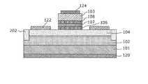
- FIG. 1is a plan view of the semiconductor device according to the first embodiment.
- FIG. 2is a cross-sectional view of the semiconductor device according to the first embodiment taken along line A-A ′ of FIG.
- FIG. 3is a plan view of the semiconductor device according to the first modification of the first embodiment.
- FIG. 4is a cross-sectional view of the semiconductor device according to Modification 1 of Embodiment 1 taken along line B-B ′ shown in FIG. 3.
- FIG. 5is a plan view of the semiconductor device according to the second modification of the first embodiment.
- FIG. 6is a cross-sectional view of the semiconductor device according to Modification 2 of Embodiment 1 taken along the line C-C ′ shown in FIG. 5.
- FIG. 5is a plan view of the semiconductor device according to the second modification of the first embodiment.
- FIG. 6is a cross-sectional view of the semiconductor device according to Modification 2 of Embodiment 1 taken along the line C-C ′ shown in FIG. 5.
- FIG. 5is
- FIG. 7is a plan view of the semiconductor device according to the third modification of the first embodiment.
- FIG. 8is a cross-sectional view of the semiconductor device according to the third modification of the first embodiment taken along the line D-D ′ shown in FIG. 7.
- FIG. 9is a plan view of the semiconductor device according to the fourth modification of the first embodiment.
- FIG. 10is a cross-sectional view of the semiconductor device according to Modification 4 of Embodiment 1 taken along the line E-E ′ shown in FIG. 9.
- FIG. 11is a plan view of the semiconductor device according to the second embodiment.
- FIG. 12is a sectional view of the semiconductor device according to the second embodiment taken along the line F-F ′ of FIG. 11.
- FIG. 13is a plan view of the semiconductor device according to the third embodiment.
- FIG. 14is a cross-sectional view of the semiconductor device according to the third embodiment taken along the line G-G ′ of FIG. 13.
- FIG. 15is a cross-sectional view of a semiconductor device according to a modification of the third embodiment.
- FIG. 16is a plan view of the semiconductor device according to the fourth embodiment.
- FIG. 17is a cross-sectional view of the semiconductor device according to the fourth embodiment taken along line H-H ′ of FIG.
- FIG. 18is a plan view of the semiconductor device according to the first modification of the fourth embodiment.
- FIG. 19is a cross-sectional view of the semiconductor device according to Modification 1 of Embodiment 4 taken along the line I-I ′ of FIG.
- FIG. 20is a plan view of a semiconductor device according to the second modification of the fourth embodiment.
- FIG. 20is a plan view of a semiconductor device according to the second modification of the fourth embodiment.
- FIG. 21is a cross-sectional view of the semiconductor device according to Modification 2 of Embodiment 4 taken along the line J-J ′ of FIG.
- FIG. 22is a plan view of a semiconductor device according to the third modification of the fourth embodiment.
- 23is a cross-sectional view of the semiconductor device according to Modification 3 of Embodiment 4 taken along the line K-K ′ of FIG.
- the first conductivity typeis N-type and the second conductivity type is P-type.
- the plan viewis hatched corresponding to the cross-sectional view.
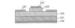
- FIG. 1is a plan view of a semiconductor device 100 according to the first embodiment.
- FIG. 2is a sectional view of the semiconductor device 100 according to the first embodiment taken along the line AA ′ in FIG.
- “plan view”means viewing from the normal direction of the main surface of the substrate 101. In order to facilitate understanding of the configuration of the semiconductor device according to the present embodiment, the plan view is given the same pattern as the cross-sectional view.
- the semiconductor device 100includes a substrate 101 having a first surface S1 and a second surface S2 facing the first surface S1, and a first nitridation disposed on the first surface S1 of the substrate 101. And a second nitride semiconductor layer disposed on the first nitride semiconductor layer.
- the substrate 101 and the first nitride semiconductor layer 102are of the first conductivity type.
- the second nitride semiconductor layer 103is of the second conductivity type.
- the semiconductor device 100corresponds to the nitride semiconductor device of the present invention.
- the semiconductor device 100includes a first electrode 120 disposed on the second surface S2 of the substrate 101, a second electrode 122 disposed on the first nitride semiconductor layer 102, a second And a gate electrode 124 disposed on the nitride semiconductor layer 103.
- the substrate 101is of the first conductivity type and is made of, for example, GaN.
- the first nitride semiconductor layer 102is of the first conductivity type, and is made of, for example, In x Al y Ga 1-xy N (0 ⁇ x ⁇ 1, 0 ⁇ y ⁇ 1, 0 ⁇ x + y ⁇ 1). Composed.
- the second nitride semiconductor layer 103is of the second conductivity type, and is made of, for example, In x Al y Ga 1-xy N (0 ⁇ x ⁇ 1, 0 ⁇ y ⁇ 1, 0 ⁇ x + y ⁇ 1). Composed.
- the first nitride semiconductor layer 102includes an acceptor impurity.
- An acceptorrefers to an atom that supplies holes.
- acceptor atoms implanted into the semiconductor layerare called acceptor impurities.
- carbon or a transition metalcan be used as the acceptor impurity.
- the carbon concentrationis preferably 1 ⁇ 10 16 / cm 2 to 1 ⁇ 10 19 / cm 2 .
- nitride semiconductor layer 102when a nitride semiconductor layer is crystal-grown, it becomes n-type naturally due to crystal defects and residual impurities acting as donors.
- the acceptor impurity contained in the first nitride semiconductor layer 102partially compensates for these donors, whereby the first nitride semiconductor layer 102 becomes highly insulating.
- the Al composition of the first nitride semiconductor layer 102 and the second nitride semiconductor layer 103(that is, the value of y in In x Al y Ga 1-xy N) is adversely affected by lattice mismatch strain with the substrate 101. It is preferable to increase the height within a range that does not appear. With this configuration, since the band gap of each layer is increased, the breakdown voltage of the semiconductor device is improved.
- the second nitride semiconductor layer 103includes, for example, magnesium.
- the magnesium concentration of the second nitride semiconductor layer 103is preferably 5 ⁇ 10 17 / cm 2 to 5 ⁇ 10 20 / cm 2 .
- the substrate 101is a first conductivity type GaN substrate
- the first nitride semiconductor layer 102is a first conductivity type GaN layer
- the second nitride semiconductor layer 103is a second conductivity type. It is assumed that it is a conductive GaN layer.
- the source electrodeis an ohmic electrode.
- the drain electrodemay be an ohmic electrode or a Schottky electrode.
- the first electrode 120is referred to as a source electrode 120 and the second electrode 122 is referred to as a drain electrode 122.
- the gate electrode 124 and the drain electrode 122are arranged side by side (in a direction parallel to the main surface of the substrate), the gate electrode 124 and the drain electrode 122 are arranged so as not to be broken due to electric field concentration on the end surface of the drain electrode 122.
- the distance between the drain electrode 122is about 20 ⁇ m. Since the highly insulating first nitride semiconductor layer 102 is formed between the source electrode 120 and the drain electrode 122, high breakdown voltage and normally-off are realized.
- the source electrodeis an ohmic electrode.
- the drain electrodemay be an ohmic electrode or a Schottky electrode.
- the first electrode 120is referred to as the drain electrode 120 and the second electrode 122 is referred to as the source electrode 122.
- a voltage of 0 Vis applied to the gate electrode 124
- a voltage of 0 Vis applied to the source electrode 122
- a voltage of +1000 Vis applied to the drain electrode 120. Since the highly insulating first nitride semiconductor layer 102 is formed between the source electrode 122 and the drain electrode 120, high breakdown voltage and normally-off are realized.
- a voltage of +3.4 V or higheris applied to the gate electrode 124. Then, holes flow from the second nitride semiconductor layer 103 into the first nitride semiconductor layer 102.
- the first nitride semiconductor layer 102is highly insulating, there are residual donors that are not completely compensated for by acceptor impurities. Light emission is generated by recombination of electrons and holes generated by the residual donor.
- the currentflows through the first insulating semiconductor layer 102 with high insulation and high withstand voltage, which should be essentially free of current by the above process, by light injection accompanying application of the gate voltage.
- a first nitride having a carbon concentration of 3 ⁇ 10 16 / cm 2 and a film thickness of 12 ⁇ mis formed by MOCVD (Metal Organic Chemical Deposition), for example.
- MOCVDMetal Organic Chemical Deposition
- a second nitride semiconductor layer 103 made of, for example, p-type GaN having a magnesium concentration of 1 ⁇ 10 19 / cm 2 and having a thickness of 500 nmis grown on the first nitride semiconductor layer 102 by MOCVD. To do.
- a resistis applied over the second nitride semiconductor layer 103 and patterned. After patterning the resist, the second nitride semiconductor layer 103 is dry etched.
- boron ionsare implanted into the first nitride semiconductor layer 102 to form the element isolation portion 202.
- an Al layer having a thickness of 200 nmis disposed on a Ti layer having a thickness of 20 nm.
- Two electrodes 122are formed.
- the first electrode 120in which an Al layer having a thickness of 200 nm is disposed on a Ti layer having a thickness of 20 nm is formed.
- a gate electrode 124is formed in which an Au layer having a thickness of 500 nm is disposed on a Ni layer having a thickness of 100 nm.
- a currentflows through the high-insulation and high-breakdown-voltage first nitride semiconductor layer 102 where the current should not substantially flow by light injection accompanying the gate voltage application.
- a group III nitride semiconductor vertical transistorhaving normally-off, high breakdown voltage, and low on-resistance can be realized.
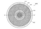
- FIG. 3is a plan view of the semiconductor device 100a according to the first modification of the first embodiment.
- 4is a cross-sectional view of the semiconductor device 100a taken along line B-B 'shown in FIG.
- the semiconductor device 100 ahas a plurality of circular second nitride semiconductor layers 103 arranged on the first nitride semiconductor layer 102 in plan view.
- a gate electrode 124is disposed on each of the plurality of second nitride semiconductor layers 103 as shown in FIG.
- a second electrode 122is disposed between the plurality of second nitride semiconductor layers 103.
- the plurality of gate electrodes 124may be electrically connected to each other.
- each second nitride semiconductor layer 103 in plan viewis not limited to a circular shape, and may be a polygonal shape such as a quadrangle. Further, the arrangement of the plurality of second nitride semiconductor layers 103 is not particularly limited as long as the apparatus operates normally.
- the area occupied by the second electrode 122 in plan viewis made larger than the area occupied by the gate electrode 124, that is, between the first electrode 120 and the second electrode 122, that is, Since the channel region between the source electrode and the drain electrode can be widened, the on-resistance can be further suppressed.
- FIG. 5is a plan view of the semiconductor device 100b according to the second modification of the first embodiment.
- 6is a cross-sectional view of the semiconductor device 100b according to the second modification of the first embodiment taken along the line C-C 'shown in FIG.
- the semiconductor device 100 bhas a plurality of circular second electrodes 122 arranged on the first nitride semiconductor layer 102 in plan view.
- a second nitride semiconductor layer 103is disposed between the plurality of second electrodes 122.
- a gate electrode 124is disposed on each of the plurality of second nitride semiconductor layers 103 as shown in FIG.
- the plurality of second electrodes 122may be electrically connected to each other.
- each second electrode 122 in plan viewis not limited to a circular shape, and may be a polygonal shape such as a quadrangle.
- the arrangement of the plurality of second electrodes 122is not particularly limited as long as the apparatus operates normally.
- the area occupied by the gate electrode 124can be made larger than the area occupied by the second electrode 122 in plan view. Therefore, since the concentration of injected holes becomes high, it becomes possible to recombine electrons and holes with higher probability.
- FIG. 7is a plan view of the semiconductor device 100c according to the third modification of the first embodiment.
- FIG. 8is a cross-sectional view of the semiconductor device 100c according to the third modification of the first embodiment taken along the line D-D ′ shown in FIG.
- the semiconductor device 100 cincludes a plurality of linear second nitride semiconductor layers 103 arranged on the first nitride semiconductor layer 102 in plan view.
- a gate electrode 124is disposed on each of the plurality of second nitride semiconductor layers 103 as shown in FIG.
- a second electrode 122is disposed between the plurality of second nitride semiconductor layers 103.
- the plurality of gate electrodes 124may be electrically connected to each other.
- the area occupied by the second electrode 122 in plan viewis made larger than the area occupied by the gate electrode 124, that is, between the first electrode 120 and the second electrode 122, that is, Since the channel region between the source electrode and the drain electrode can be widened, the on-resistance can be further suppressed.
- FIG. 9is a plan view of the semiconductor device 100d according to the fourth modification of the first embodiment.
- FIG. 10is a cross-sectional view of the semiconductor device 100d according to the fourth modification of the first embodiment taken along the line E-E 'shown in FIG.
- a plurality of linear second electrodes 122are arranged on the first nitride semiconductor layer 102 in plan view.
- a second nitride semiconductor layer 103is disposed between the plurality of second electrodes 122.
- a gate electrode 124is disposed on each of the plurality of second nitride semiconductor layers 103 as shown in FIG.
- the plurality of second electrodes 122may be electrically connected to each other.
- the semiconductor device 100deven when the emission intensity under the gate electrode 124 is weakened by making the area occupied by the gate electrode 124 larger than the area occupied by the second electrode 122 in plan view, The light emitting area can be widened. Therefore, in the semiconductor device 100d, since the concentration of injected holes is high, it is possible to flow current more effectively by recombining electrons and holes with higher probability. Note that the case where the emission intensity becomes weak is assumed, for example, when the Al composition of the first nitride semiconductor layer 102 or the second nitride semiconductor layer 103 is increased in order to increase the breakdown voltage.
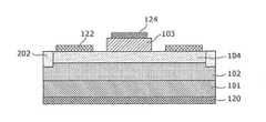
- FIG. 11is a plan view of the semiconductor device 200 according to the second embodiment.
- FIG. 12is a cross-sectional view of the semiconductor device 200 according to the second embodiment taken along the line F-F ′ of FIG. 11.
- the semiconductor device 200 according to the second embodimentis arranged between the first nitride semiconductor layer 102 and the second nitride semiconductor layer 103, and as shown in FIG. A third nitride semiconductor layer 104 containing a donor impurity is further provided.
- a material of the third nitride semiconductor layer 104for example, GaN may be used.
- the silicon concentrationmay be, for example, 1 ⁇ 10 17 / cm 2 or more.
- the film thickness of the third nitride semiconductor layer 104may be 100 nm, for example.
- the first electrode 120may be a drain electrode and the second electrode 122 may be a source electrode. Further, the first electrode 120 may be a source electrode, and the second electrode 122 may be a drain electrode.
- the third nitride semiconductor layer 104may be formed by MOCVD, for example, after the formation of the first nitride semiconductor layer 102 and before the formation of the second nitride semiconductor layer 103. .
- the semiconductor device 200 according to the second embodimentcan emit light with higher efficiency than the semiconductor device 100 according to the first embodiment, the on-resistance is lower than that of the semiconductor device 100 according to the first embodiment. be able to.
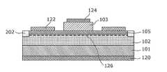
- FIG. 13is a plan view of the semiconductor device 300 according to the third embodiment
- FIG. 14is a cross-sectional view of the semiconductor device 300 according to the third embodiment taken along the line G-G ′ of FIG.
- the semiconductor device 300is disposed between the first nitride semiconductor layer 102 and the second nitride semiconductor layer 103 and has a band gap larger than that of the first nitride semiconductor layer 102.
- the fourth nitride semiconductor layer 105 having a large thicknessis provided.
- the first nitride semiconductor layer 102is made of GaN
- Al 0.3 Ga 0.7 Nmay be used as the material of the fourth nitride semiconductor layer 105.
- the film thickness of Al 0.3 Ga 0.7 Nmay be about 20 nm, for example.
- the first electrode 120may be a drain electrode and the second electrode 122 may be a source electrode. Further, the first electrode 120 may be a source electrode, and the second electrode 122 may be a drain electrode.
- the fourth nitride semiconductor layer 105may be formed by MOCVD.
- a high-density two-dimensional electron gas 126is formed between the first nitride semiconductor layer 102 and the fourth nitride semiconductor layer 105 by spontaneous polarization and piezoelectric polarization. Therefore, when a voltage is applied to the gate electrode 124, holes are injected into the two-dimensional electron gas 126, whereby high-density electrons and holes can be recombined.
- the semiconductor device 300 according to the third embodimentcan emit light with higher efficiency than the semiconductor device 100 according to the first embodiment, the on-resistance can be lowered as compared with the first embodiment.
- the third nitride semiconductor layer 104 described in Embodiment 2is used between the second nitride semiconductor layer 103 and the fourth nitride semiconductor layer 105 or between the first nitride semiconductor layer 102 and the fourth nitride. It may be disposed anywhere between the physical semiconductor layer 105.
- FIG. 15is a sectional view of a semiconductor device 300a according to a modification of the third embodiment. Although a plan view of the semiconductor device 300a is omitted, the configuration is substantially the same as that of the semiconductor device 300 shown in FIG.
- the semiconductor device 300 ais provided with a first recess 128 that penetrates the fourth nitride semiconductor layer 105 and reaches at least the first nitride semiconductor layer 102.
- a second electrode 122is disposed in the first recess 128.
- the second electrode 122is preferably in contact with the two-dimensional electron gas 126.
- a resistis applied to the fourth nitride semiconductor layer 105 and patterned. After patterning the resist, the fourth recess semiconductor layer 105 and the first nitride semiconductor layer 102 may be dry-etched to form the first recess 128.
- FIG. 16is a plan view of the semiconductor device 400 according to the fourth embodiment.
- FIG. 17is a cross-sectional view of the semiconductor device 400 according to the fourth embodiment taken along the line H-H ′ of FIG. 16.
- the semiconductor device 400is located between the first nitride semiconductor layer 102 and the second nitride semiconductor layer 103 from the first nitride semiconductor layer 102 side.
- a fifth nitride semiconductor layer 106, a sixth nitride semiconductor layer 107, and a seventh nitride semiconductor layer 108are stacked in this order.
- the band gap of the fifth nitride semiconductor layer 106is greater than or equal to the band gap of the first nitride semiconductor layer 102.
- the band gap of the sixth nitride semiconductor layer 107is smaller than the band gap of the fifth nitride semiconductor layer 106.
- the band gap of the seventh nitride semiconductor layer 108is greater than or equal to the band gap of the first nitride semiconductor layer 102 and larger than the band gap of the sixth nitride semiconductor layer 106. Note that the fifth nitride semiconductor layer 106 and the seventh nitride semiconductor layer 108 may be made of the same material.
- the first electrode 120may be a drain electrode and the second electrode 122 may be a source electrode. Further, the first electrode 120 may be a source electrode, and the second electrode 122 may be a drain electrode.
- quantum levelsare formed in the sixth nitride semiconductor layer 107 by the electron and hole confinement effect of the fifth nitride semiconductor layer 106 and the seventh nitride semiconductor layer 108.
- the probability of recombination of electrons and holesis improved.
- the semiconductor device 400 according to the fourth embodimentcan emit light with higher efficiency than the semiconductor device 100 according to the first embodiment, the on-resistance is lower than that of the semiconductor device 100 according to the first embodiment. be able to.
- the fifth nitride semiconductor layer 106, the sixth nitride semiconductor layer 107, and the seventh nitride semiconductor layer 108may have a multiple quantum well (MQW) structure formed sequentially and repeatedly. It is desirable that there are three layers of the sixth nitride semiconductor layer 107 in which a period, that is, a quantum level is formed.
- MQWmultiple quantum well
- the fifth nitride semiconductor layer 106 and the seventh nitride semiconductor layer 108are made of, for example, Al 0.1 Ga 0.9 N having a thickness of 10 nm.
- the sixth nitride semiconductor layer 107is made of, for example, GaN having a thickness of 3 nm.
- the fifth nitride semiconductor layer 106 and the sixth nitride semiconductorare formed by MOCVD.
- the layer 107 and the seventh nitride semiconductor layer 108may be formed sequentially.
- a resistis applied over the second nitride semiconductor layer 103 and patterned.
- the second nitride semiconductor layer 103, the fifth nitride semiconductor layer 106, the sixth nitride semiconductor layer 107, and the seventh nitride semiconductor layer 108are dry-etched to thereby form the first nitride semiconductor layer 102. To expose.
- the semiconductor device 400 according to the fourth embodimentcan emit light with high efficiency, the on-resistance can be lowered as compared with the semiconductor device 100 according to the first embodiment.
- FIG. 18is a plan view of a semiconductor device 400a according to the first modification of the fourth embodiment.
- FIG. 19is a cross-sectional view of the semiconductor device 400 according to Modification 1 of Embodiment 4 taken along the line I-I ′ of FIG.
- the second electrode 122is formed in the second recess 129 formed in the first nitride semiconductor layer 102, and the fifth The nitride semiconductor layer 106, the sixth nitride semiconductor layer 107, and the seventh nitride semiconductor layer 108 are in contact with the side surfaces.
- a two-dimensional electron gas (not shown) formed at the interface between the fifth nitride semiconductor layer 106 and the first nitride semiconductor layer 102 and the second electrode 122come into contact with each other, whereby the first nitride semiconductor layer 102 is contacted.
- the contact resistance between the first electrode 122 and the second electrode 122can be reduced. Thereby, the on-resistance of the semiconductor device 400a can be further reduced.
- FIG. 20is a plan view of the semiconductor device 400b according to the second modification of the fourth embodiment.
- FIG. 21is a cross-sectional view of the semiconductor device 400b according to Modification 2 of Embodiment 4 taken along the line J-J 'of FIG.
- third nitridation including a donor impurity such as siliconis provided between the first nitride semiconductor layer 102 and the fifth nitride semiconductor layer 106.
- a physical semiconductor layer 104may be formed.
- FIG. 22is a plan view of a semiconductor device 400c according to the third modification of the fourth embodiment.
- FIG. 23is a cross-sectional view of the semiconductor device 400c according to Modification 3 of Embodiment 4 taken along the line K-K ′ of FIG.
- the difference between the semiconductor device 400c according to the present modification and the semiconductor device 400b according to the second modificationis that, as shown in FIGS. 22 and 23, the side surface of the third nitride semiconductor layer 104 is the fifth nitride semiconductor layer 106.
- the sixth nitride semiconductor layer 107, the seventh nitride semiconductor layer 108, and the second nitride semiconductor layer 103are formed on substantially the same plane.
- substantially the samemeans that a manufacturing error is included.
- the semiconductor device 400chas a shorter distance between the source electrode and the drain electrode than the semiconductor device 400b according to the second modification, and the third nitride semiconductor layer 104 to the sixth nitride semiconductor layer 107. Higher density electrons can flow. As a result, the probability that electrons and holes are recombined in the quantum level of the sixth nitride semiconductor layer 107 is further improved. Therefore, the semiconductor device 400c can further reduce the on-resistance by emitting light with higher efficiency.
- the first conductivity typeis the N type and the second conductivity type is the P type, but the first conductivity type is the P type and the second conductivity type is the N type. It is good.
- each nitride semiconductor layer in plan viewis not limited to a circular shape, and may be a polygonal shape such as a quadrangle.
- the arrangement of the plurality of nitride semiconductor layersis not particularly limited as long as the device operates normally.
- the nitride semiconductor device according to the present inventioncan be used as a high-output, high-breakdown-voltage transistor used in a power supply circuit for consumer equipment.
Landscapes
- Junction Field-Effect Transistors (AREA)
Abstract
Description
Translated fromJapanese本開示は、半導体装置、特に窒化物半導体装置に関する。The present disclosure relates to a semiconductor device, particularly a nitride semiconductor device.
三族窒化物半導体は、シリコン(Si)などの従来の半導体よりもバンドギャップ及び絶縁破壊電界が大きいため、高耐圧トランジスタの材料として有望である。三族窒化物半導体トランジスタの構造においては、三族窒化物半導体のヘテロ接合界面に生じる2次元電子ガスをチャネルとして用いる横型トランジスタが一般的である。しかしながら、横型トランジスタはそれぞれの電極が表面に平面的に並ぶ構造であるため、ドレイン電極端面に電界集中が発生して耐圧が低下しやすい。一方、ソース電極を表面側に、ドレイン電極を基板側に設置する縦型トランジスタならば、ドレイン電極に均一に電界がかかるため、高耐圧が期待できる(例えば、特許文献1参照)。Group III nitride semiconductors are promising as materials for high voltage transistors because they have a larger band gap and dielectric breakdown field than conventional semiconductors such as silicon (Si). In the structure of a group III nitride semiconductor transistor, a lateral transistor using a two-dimensional electron gas generated at a heterojunction interface of a group III nitride semiconductor as a channel is generally used. However, since the lateral transistor has a structure in which the respective electrodes are arranged in a plane on the surface, electric field concentration occurs on the end surface of the drain electrode, and the breakdown voltage tends to decrease. On the other hand, in the case of a vertical transistor in which the source electrode is provided on the front side and the drain electrode is provided on the substrate side, a high breakdown voltage can be expected because an electric field is uniformly applied to the drain electrode (see, for example, Patent Document 1).
三族窒化物半導体縦型トランジスタは、高耐圧かつ低オン抵抗であるとともに、デバイス動作時の安全性の点からノーマリオフであることが要請される。三族窒化物半導体縦型トランジスタのチャネルには、一般的に、ドナーとして、例えば、Siをドーピングしたn型GaN層を用いる。このとき、オン抵抗を低くするためにSiドーピング濃度を高くしすぎると、多量の結晶欠陥が形成されるため、耐圧が著しく低下する。また、ソース電極とドレイン電極との間に電流が流れやすくなるため、該縦型トランジスタは、ノーマリオンとなる。一方、ノーマリオフや高耐圧化のためにSiドーピング濃度を低くすると、オン抵抗が高くなる。従って、従来の三族窒化物半導体縦型トランジスタにおいて、ノーマリオフ、低オン抵抗かつ高耐圧を両立することが非常に困難であった。The group III nitride semiconductor vertical transistor is required to have a high breakdown voltage and a low on-resistance, and to be normally off from the viewpoint of safety during device operation. For the channel of the group III nitride semiconductor vertical transistor, for example, an n-type GaN layer doped with Si is generally used as a donor. At this time, if the Si doping concentration is increased too much in order to reduce the on-resistance, a large amount of crystal defects are formed, and the breakdown voltage is significantly reduced. In addition, since a current easily flows between the source electrode and the drain electrode, the vertical transistor is normally on. On the other hand, when the Si doping concentration is lowered for normally-off or high breakdown voltage, the on-resistance increases. Therefore, it has been very difficult to achieve both normally-off, low on-resistance and high breakdown voltage in the conventional group III nitride semiconductor vertical transistor.
上記課題に鑑み、本発明は、ノーマリオフ、高耐圧かつ低オン抵抗の三族窒化物半導体縦型トランジスタを実現することができる窒化物半導体装置を提供することを目的とする。In view of the above problems, an object of the present invention is to provide a nitride semiconductor device capable of realizing a group III nitride semiconductor vertical transistor having normally-off, high breakdown voltage, and low on-resistance.
上述した課題を達成するため、本発明の一態様にかかる窒化物半導体装置は、第1導電型の基板であって、第1面と、前記第1面と対向する第2面とを有する基板と、前記基板の前記第1面上に配置され、アクセプタ不純物を含む、前記第1導電型の第1窒化物半導体層と、前記第1窒化物半導体層の上に配置され、前記第1導電型と逆導電型の第2導電型の第2窒化物半導体層と、前記基板の前記第2面上に配置された第1電極と、前記第1窒化物半導体層の上に配置された第2電極と、前記第2窒化物半導体層の上に配置されたゲート電極とを備える。In order to achieve the above-described problem, a nitride semiconductor device according to an aspect of the present invention is a first conductivity type substrate, which has a first surface and a second surface opposite to the first surface. A first nitride semiconductor layer of the first conductivity type disposed on the first surface of the substrate and containing an acceptor impurity; and disposed on the first nitride semiconductor layer; and A second conductivity type second nitride semiconductor layer of a reverse conductivity type, a first electrode disposed on the second surface of the substrate, and a first electrode disposed on the first nitride semiconductor layer. Two electrodes, and a gate electrode disposed on the second nitride semiconductor layer.
本開示によれば、ノーマリオフ、高耐圧かつ低オン抵抗の三族窒化物半導体縦型トランジスタを実現することができる。According to the present disclosure, a group III nitride semiconductor vertical transistor having normally-off, high breakdown voltage, and low on-resistance can be realized.
以下、本開示に係る窒化物半導体装置の形態について、図面を参照しながら具体的に説明する。実質的に同一の構成に対して同一の符号を付し、説明を省略する場合がある。また、以下の実施の形態において、製造方法が実質的に同一であるときは、説明を省略する場合がある。Hereinafter, embodiments of the nitride semiconductor device according to the present disclosure will be specifically described with reference to the drawings. The substantially same configuration may be denoted by the same reference numeral, and the description may be omitted. In the following embodiments, when the manufacturing method is substantially the same, the description may be omitted.
本開示は、以下の実施の形態に限定されない。本開示の実施の形態及び変形例同士を組合せることも可能である。以下で説明する実施の形態は、いずれも一具体例を示すものである。以下の実施の形態で示される数値、形状、材料、構成要素、構成要素の配置位置及び接続形態等は、一例であり、本発明を限定する主旨ではない。以下の実施の形態における構成要素のうち、独立請求項に記載されていない構成要素については、本発明の課題を達成するのに必ずしも必要ではないが、より好ましい形態を構成するものとして説明される。This disclosure is not limited to the following embodiment. Embodiments and modifications of the present disclosure may be combined. Each of the embodiments described below shows one specific example. The numerical values, shapes, materials, constituent elements, arrangement positions and connecting forms of the constituent elements shown in the following embodiments are merely examples, and are not intended to limit the present invention. Among the constituent elements in the following embodiments, constituent elements that are not described in the independent claims are not necessarily required to achieve the object of the present invention, but are described as constituting more preferable embodiments. .
以下の実施の形態にかかる半導体装置において、第1導電型がN型であり、第2導電型がP型である。また、実施の形態にかかる半導体装置の構成の理解を容易にするために、平面図には、断面図に対応するハッチングを付している。In the semiconductor device according to the following embodiments, the first conductivity type is N-type and the second conductivity type is P-type. In order to facilitate understanding of the configuration of the semiconductor device according to the embodiment, the plan view is hatched corresponding to the cross-sectional view.
(実施の形態1)
以下、本開示における窒化物半導体装置の一態様として、実施の形態1にかかる半導体装置100について説明する。(Embodiment 1)
Hereinafter, the
[1.半導体装置の構造]
図1は、実施の形態1に係る半導体装置100の平面図である。図2は、図1のA-A’線における実施の形態1に係る半導体装置100の断面図である。本開示において、「平面視」とは、基板101の主面の法線方向から見ることを意味する。また、本実施の形態にかかる半導体装置の構成の理解を容易にするために、平面図には、断面図と同様の模様を付している。[1. Structure of semiconductor device]
FIG. 1 is a plan view of a
実施の形態1に係る半導体装置100は、第1面S1と、第1面S1と対向する第2面S2とを有する基板101と、基板101の第1面S1上に配置された第1窒化物半導体層102と、第1窒化物半導体層102の上に配置された第2窒化物半導体層とを備える。基板101及び第1窒化物半導体層102は、第1導電型である。第2窒化物半導体層103は、第2導電型である。The
ここで、半導体装置100は、本発明の窒化物半導体装置に相当する。Here, the
実施の形態1に係る半導体装置100は、基板101の第2面S2上に配置された第1電極120と、第1窒化物半導体層102の上に配置された第2電極122と、第2窒化物半導体層103の上に配置されたゲート電極124とを備える。The
基板101は、第1導電型であって、例えば、GaNから構成される。第1窒化物半導体層102は、第1導電型であって、例えば、InxAlyGa1-x-yN(0≦x≦1、0≦y≦1、0≦x+y≦1)から構成される。第2窒化物半導体層103は、第2導電型であって、例えば、InxAlyGa1-x-yN(0≦x≦1、0≦y≦1、0≦x+y≦1)から構成される。The
第1窒化物半導体層102は、アクセプタ不純物を含む。アクセプタとは、正孔を供給する原子のことをいう。本開示では、半導体層に注入されるアクセプタ原子をアクセプタ不純物と呼んでいる。アクセプタ不純物としては、例えば、炭素や遷移金属を用いることができる。第1窒化物半導体層102が炭素を含む場合、炭素濃度は、1×10¹⁶/cm2から1×1019/cm2であることが好ましい。The first
一般的に、窒化物半導体層を結晶成長する場合、結晶欠陥や残留不純物がドナーとして働くことによって、自然にn型となる。第1窒化物半導体層102に含まれるアクセプタ不純物が、これらのドナーを部分的に補償することによって、第1窒化物半導体層102は、高絶縁性となる。In general, when a nitride semiconductor layer is crystal-grown, it becomes n-type naturally due to crystal defects and residual impurities acting as donors. The acceptor impurity contained in the first
第1窒化物半導体層102及び第2窒化物半導体層103のAl組成(すなわち、InxAlyGa1-x-yNにおけるyの値)は、基板101との格子不整合歪みによる悪影響が出ない範囲において、高くすることが好ましい。この構成によって、各層のバンドギャップが増大するため、半導体装置の耐圧が向上する。The Al composition of the first
第2窒化物半導体層103は、例えば、マグネシウムを含む。第2窒化物半導体層103のマグネシウム濃度は、5×10¹⁷/cm2から5×1020/cm2であることが好ましい。The second
実施の形態1に係る半導体装置では、一例として、基板101は第1導電型のGaN基板、第1窒化物半導体層102は第1導電型のGaN層、第2窒化物半導体層103は第2導電型のGaN層であるとする。In the semiconductor device according to the first embodiment, as an example, the
[2.半導体装置の動作]
[2-1.パターン1]
ここでは、第1電極120がソース電極であり、第2電極122がドレイン電極である場合の半導体装置100の動作について説明する。ソース電極は、オーミック電極である。ドレイン電極は、オーミック電極であっても良いし、ショットキー電極であっても良い。以下、理解を容易にするために、第1電極120をソース電極120と呼び、第2電極122をドレイン電極122と呼ぶ。[2. Operation of Semiconductor Device]
[2-1. Pattern 1]
Here, the operation of the
実施の形態1に係る半導体装置100において、例えば、ゲート電極124に0V、ソース電極120に0V、ドレイン電極122に+1000Vの電圧が印加されているとする。ここで、ゲート電極124とドレイン電極122とは横(基板の主面に平行な方向)に並ぶこととなるため、ドレイン電極122端面への電界集中による破壊が生じないように、ゲート電極124とドレイン電極122との間の距離は、20μm程度とする。ソース電極120とドレイン電極122との間には高絶縁性の第1窒化物半導体層102が形成されているため、高耐圧かつノーマリオフが実現される。In the
次に、ゲート電極124に+3.4V以上の電圧を印加すると、第2窒化物半導体層103から第1窒化物半導体層102に正孔が流入する。基板101はn型GaN層であり、第1電極120はソース電極であるため、基板101から第1窒化物半導体層102に電子が流入する。Next, when a voltage of +3.4 V or higher is applied to the
第1窒化物半導体層102には、電子と正孔とが注入されるため、互いに再結合して発光する。発せられた光のエネルギーが、第1窒化物半導体層102を構成する材料のバンドギャップと同等以上であれば、第1窒化物半導体層102に直ちに吸収され、電子と正孔との対が形成される。ソース電極120とドレイン電極122との間において、第1窒化物半導体層102には、高電界が印加されているため、これらの電子と正孔との対が再結合する前に、正孔はソース電極120側に、電子はドレイン電極122側に乖離する。乖離した電子-正孔流が電流となる。Since electrons and holes are injected into the first
ゲート電極124に電圧が印加されている限り発光は継続するため、電流が流れ続ける。ゲート電極124の電圧を0Vとすると、発光が止まり、ソース電極120とドレイン電極との122間に流れる電流はゼロとなる。As long as a voltage is applied to the
上記の過程により、本来は電流が実質流れないはずの高絶縁性かつ高耐圧の第1窒化物半導体層102には、ゲート電圧印加に伴う光注入により電流が流れる。以上の構成から、高耐圧で低オン抵抗かつノーマリオフでのスイッチングが可能となる。Through the above process, current flows through the first insulating
[2-2.パターン2]
ここでは、第1電極120がドレイン電極、第2電極122がソース電極である場合の半導体装置100の動作について説明する。ソース電極は、オーミック電極である。ドレイン電極は、オーミック電極であっても良いし、ショットキー電極であっても良い。以下、理解を容易にするために、第1電極120をドレイン電極120と呼び、第2電極122をソース電極122と呼ぶ。[2-2. Pattern 2]
Here, an operation of the
例えば、ゲート電極124に0V、ソース電極122に0V、ドレイン電極120に+1000Vの電圧が印加されているとする。ソース電極122とドレイン電極120との間には高絶縁性の第1窒化物半導体層102が形成されているため、高耐圧かつノーマリオフが実現される。For example, assume that a voltage of 0 V is applied to the
次に、ゲート電極124に+3.4V以上の電圧を印加する。すると、第2窒化物半導体層103から第1窒化物半導体層102に正孔が流入する。第1窒化物半導体層102は高絶縁性ではあるものの、アクセプタ不純物により補償しきれていない残留ドナーが存在する。この残留ドナーによって生じた電子と、正孔とが再結合することによって発光が生じる。Next, a voltage of +3.4 V or higher is applied to the
このような構成により、パターン1と同様に、半導体装置100では、第1窒化物半導体層102に光が吸収され、電子と正孔との対となる。該電子と正孔との対がソース電極122とドレイン電極120との間の電界によって乖離し、電流となる。ゲート電極124の電圧を0Vとすると発光が止まり、ソース電極122とドレイン電極120との間の電流はゼロとなる。With such a configuration, similarly to the pattern 1, in the
また、パターン1と同様に、上記の過程により、本来は電流が実質流れないはずの高絶縁かつ高耐圧の第1窒化物半導体層102には、ゲート電圧印加に伴う光注入により電流が流れる。以上の構成から、高耐圧で低オン抵抗かつノーマリオフでのスイッチングが可能となる。Similarly to the pattern 1, the current flows through the first insulating
[3.半導体装置の製造方法]
実施の形態1に係る半導体装置の製造方法を説明する。なお、製造方法の順序は、一例であり、下記の順序には限定されず、当業者が適宜改変することが可能である。[3. Manufacturing method of semiconductor device]
A method for manufacturing the semiconductor device according to the first embodiment will be described. Note that the order of the manufacturing method is an example, and is not limited to the following order, and can be appropriately modified by those skilled in the art.
まず、GaNからなる基板101の主面上に、MOCVD(Metal Organic Chemical Vapor Deposition)法により、例えば、炭素濃度が3×10¹⁶/cm2のGaNからなり、膜厚が12μmの第1窒化物半導体層102を形成する。First, on the main surface of the
次に、第1窒化物半導体層102上に、MOCVD法により、例えば、マグネシウム濃度が1×10¹⁹/cm2のp型GaNからなり、膜厚が500nmの第2窒化物半導体層103を成長する。Next, a second
次に、第2窒化物半導体層103の上方にレジストを塗布し、パターニングを行う。レジストをパターニングした後に、第2窒化物半導体層103をドライエッチングする。Next, a resist is applied over the second
次に、例えば、ボロンイオンを第1窒化物半導体層102に注入することによって、素子分離部202を形成する。Next, for example, boron ions are implanted into the first
次に、第2窒化物半導体層103をドライエッチングすることにより露出した第1窒化物半導体層102上に、例えば、膜厚が20nmのTi層上に膜厚が200nmのAl層を配置した第2電極122を形成する。Next, on the first
次に、基板101の第2面S2上に、例えば、膜厚が20nmのTi層上に、膜厚が200nmのAl層を配置した第1電極120を形成する。Next, on the second surface S2 of the
次に、第2窒化物半導体層103上に、例えば、膜厚が100nmのNi層上に、膜厚が500nmのAu層を配置したゲート電極124を形成する。Next, on the second
[4.効果]
以上、本実施の形態にかかる半導体装置100によると、電流が実質流れないはずの高絶縁かつ高耐圧の第1窒化物半導体層102に、ゲート電圧印加に伴う光注入により電流が流れる。これにより、ノーマリオフ、高耐圧かつ低オン抵抗の三族窒化物半導体縦型トランジスタを実現することができる。[4. effect]
As described above, according to the
(実施の形態1の変形例1)
次に、実施の形態1の変形例1に係る半導体装置100aについて説明する。(Modification 1 of Embodiment 1)
Next, a
図3は、実施の形態1の変形例1に係る半導体装置100aの平面図である。図4は、図3で示されたB-B’線における半導体装置100aの断面図である。FIG. 3 is a plan view of the
図3に示すように、本変形例にかかる半導体装置100aは、平面視において、円形状の第2窒化物半導体層103が複数、第1窒化物半導体層102の上に配置されている。複数の第2窒化物半導体層103のそれぞれの上には、図4に示すように、ゲート電極124が配置されている。そして、複数の第2窒化物半導体層103の間には、第2電極122が配置されている。複数のゲート電極124は、互いに電気的に接続されていてもよい。As shown in FIG. 3, the
なお、各第2窒化物半導体層103の平面視における形状は、円形状に限らず、四角形等の多角形状であってもよい。また、複数の第2窒化物半導体層103の配置の仕方は、装置が正常に動作する限り、特に制限はない。It should be noted that the shape of each second
本変形例にかかる半導体装置100aでは、平面視において、第2電極122が占める面積を、ゲート電極124が占める面積よりも大きくすることによって、第1電極120と第2電極122との間、つまり、ソース電極とドレイン電極との間のチャネル領域を広くすることができるため、オン抵抗をさらに抑えることができる。In the
(実施の形態1の変形例2)
次に、実施の形態1の変形例2に係る半導体装置100bについて説明する。(Modification 2 of Embodiment 1)
Next, a
図5は、実施の形態1の変形例2に係る半導体装置100bの平面図である。図6は、図5で示されたC-C’線における、実施の形態1の変形例2に係る半導体装置100bの断面図である。FIG. 5 is a plan view of the
図5に示すように、本変形例にかかる半導体装置100bは、平面視において、円形状の第2電極122が複数、第1窒化物半導体層102の上に配置されている。そして、複数の第2電極122の間には、第2窒化物半導体層103が配置されている。複数の第2窒化物半導体層103のそれぞれの上には、図6に示すように、ゲート電極124が配置されている。複数の第2電極122は、互いに電気的に接続されていてもよい。As shown in FIG. 5, the
なお、各第2電極122の平面視における形状は、円形状に限らず、四角形等の多角形状であってもよい。また、複数の第2電極122の配置の仕方は、装置が正常に動作する限り、特に制限はない。Note that the shape of each
本変形例にかかる半導体装置100bでは、平面視において、ゲート電極124が占める面積を、第2電極122が占める面積よりも大きくすることができる。したがって、注入される正孔の濃度が高くなるため、より高確率で電子と正孔とを再結合させることが可能となる。In the
(実施の形態1の変形例3)
次に、実施の形態1の変形例3に係る半導体装置100cについて説明する。(
Next, a
図7は、実施の形態1の変形例3に係る半導体装置100cの平面図である。図8は、図7で示されたD-D’線における、実施の形態1の変形例3に係る半導体装置100cの断面図である。FIG. 7 is a plan view of the
図7に示すように、本変形例にかかる半導体装置100cは、平面視において、直線状の第2窒化物半導体層103が複数、第1窒化物半導体層102上に配置されている。複数の第2窒化物半導体層103のそれぞれの上には、図8に示すように、ゲート電極124が配置されている。そして、複数の第2窒化物半導体層103の間には、第2電極122が配置されている。複数のゲート電極124は、互いに電気的に接続されていてもよい。As shown in FIG. 7, the
本変形例にかかる半導体装置100cでは、平面視において、第2電極122が占める面積を、ゲート電極124が占める面積よりも大きくすることによって、第1電極120と第2電極122との間、つまり、ソース電極とドレイン電極との間のチャネル領域を広くすることができるため、オン抵抗をさらに抑えることができる。In the
(実施の形態1の変形例4)
次に、実施の形態1の変形例4に係る半導体装置100dについて説明する。(Modification 4 of Embodiment 1)
Next, a
図9は、実施の形態1の変形例4に係る半導体装置100dの平面図である。図10は、図9で示されたE-E’線における、実施の形態1の変形例4に係る半導体装置100dの断面図である。FIG. 9 is a plan view of the
図9に示すように、本変形例にかかる半導体装置100dは、平面視において、直線状の第2電極122が複数、第1窒化物半導体層102上に配置されている。そして、複数の第2電極122の間には、第2窒化物半導体層103が配置されている。複数の第2窒化物半導体層103のそれぞれの上には、図10に示すように、ゲート電極124が配置されている。複数の第2電極122は、互いに電気的に接続されていてもよい。As shown in FIG. 9, in the
本変形例にかかる半導体装置100dでは、平面視において、ゲート電極124が占める面積を、第2電極122が占める面積よりも大きくすることによって、ゲート電極124下での発光強度が弱くなる場合でも、発光領域を広くすることができる。したがって、半導体装置100dでは、注入される正孔の濃度が高くなるため、より高確率で電子と正孔とを再結合させて有効に電流を流すことが可能となる。なお、発光強度が弱くなる場合とは、例えば、高耐圧化のために第1窒化物半導体層102や第2窒化物半導体層103のAl組成を高くした場合などが想定される。In the
(実施の形態2)
次に、実施の形態2に係る半導体装置200について説明する。(Embodiment 2)
Next, the
図11は、実施の形態2に係る半導体装置200の平面図である。図12は、図11のF-F’線における実施の形態2に係る半導体装置200の断面図である。FIG. 11 is a plan view of the
図11に示すように、実施の形態2に係る半導体装置200は、第1窒化物半導体層102と第2窒化物半導体層103との間に配置され、図12に示すように、シリコン等のドナー不純物を含む第3窒化物半導体層104をさらに備えている。第3窒化物半導体層104の材料としては、例えば、GaNを用いればよい。シリコン濃度は、例えば、1×10¹⁷/cm2以上であればよい。第3窒化物半導体層104の膜厚は、例えば、100nmであればよい。As shown in FIG. 11, the
半導体装置200において、第1電極120がドレイン電極であり、第2電極122がソース電極であってもよい。また、第1電極120がソース電極であり、第2電極122がドレイン電極であってもよい。In the
半導体装置200の製造方法に関しては、第1窒化物半導体層102の形成後、第2窒化物半導体層103の形成前に、例えば、MOCVD法により、第3窒化物半導体層104を形成すればよい。Regarding the method for manufacturing the
また、第3窒化物半導体層104内には、ドナー不純物により高密度の電子が存在するため、電子と正孔とが再結合する確率が上昇する。In addition, since there are high-density electrons in the third
従って、実施の形態2に係る半導体装置200においては、実施の形態1に係る半導体装置100よりも高効率で発光させることができるため、実施の形態1にかかる半導体装置100よりもオン抵抗を下げることができる。Therefore, since the
(実施の形態3)
次に、実施の形態3に係る半導体装置300について説明する。(Embodiment 3)
Next, the
図13は、実施の形態3に係る半導体装置300の平面図であり、図14は、図13のG-G’線における実施の形態3に係る半導体装置300の断面図である。13 is a plan view of the
図13に示すように、実施の形態3に係る半導体装置300は、第1窒化物半導体層102と第2窒化物半導体層103の間に配置され、第1窒化物半導体層102よりもバンドギャップが大きい第4窒化物半導体層105を備えている。第1窒化物半導体層102がGaNからなる場合は、第4窒化物半導体層105の材料は、例えば、Al0.3Ga0.7Nを用いれば良い。Al0.3Ga0.7Nの膜厚は、例えば約20nmであればよい。As shown in FIG. 13, the
半導体装置300において、第1電極120がドレイン電極であり、第2電極122がソース電極であってもよい。また、第1電極120がソース電極であり、第2電極122がドレイン電極であってもよい。In the
半導体装置300の製造方法に関しては、第1窒化物半導体層102の形成後、第2窒化物半導体層103の形成前に、例えば、MOCVD法により第4窒化物半導体層105を形成すればよい。Regarding the manufacturing method of the
また、図14に示すように、第1窒化物半導体層102と第4窒化物半導体層105との間には、自発分極と圧電分極により高密度の2次元電子ガス126が形成される。そのため、ゲート電極124に電圧を印加すると、2次元電子ガス126に正孔が注入されることによって、高密度の電子と正孔を再結合させることができる。Further, as shown in FIG. 14, a high-density two-
従って、実施の形態3に係る半導体装置300においては、実施の形態1に係る半導体装置100よりも高効率で発光させることができるため、実施の形態1よりもオン抵抗を下げることができる。Therefore, since the
なお、本実施の形態と実施の形態2との組み合わせも可能である。つまり、実施の形態2に示した第3窒化物半導体層104を、第2窒化物半導体層103と第4窒化物半導体層105との間、又は、第1窒化物半導体層102と第4窒化物半導体層105との間の、いずれに配置してもよい。Note that a combination of the present embodiment and the second embodiment is also possible. That is, the third
(実施の形態3の変形例)
次に、実施の形態3の変形例に係る半導体装置300aについて説明する。(Modification of Embodiment 3)
Next, a
図15は、実施の形態3の変形例に係る半導体装置300aの断面図を示す。半導体装置300aの平面図は省略するが、図13に示した半導体装置300と実質同じ構成である。FIG. 15 is a sectional view of a
本変形例に係る半導体装置300aは、図13に示すように、第4窒化物半導体層105を貫通し、少なくとも第1窒化物半導体層102に到達する第1リセス128が設けられている。第1リセス128内には、第2電極122が配置されている。第2電極122は、2次元電子ガス126と接触させることが好ましい。この構成により、第1窒化物半導体層102と第2電極122とのコンタクト抵抗を低くすることができるため、オン抵抗をさらに下げることができる。As shown in FIG. 13, the
半導体装置300aの製造方法に関しては、例えば、第2窒化物半導体層103のドライエッチング後、第4窒化物半導体層105に対してレジストを塗布し、パターニングを行う。レジストをパターニングした後、第4窒化物半導体層105、及び、第1窒化物半導体層102をドライエッチングして、第1リセス128を形成すればよい。Regarding the manufacturing method of the
(実施の形態4)
次に、実施の形態4に係る半導体装置400について説明する。(Embodiment 4)
Next, a
図16は、実施の形態4に係る半導体装置400の平面図である。図17は、図16のH-H’線における実施の形態4に係る半導体装置400の断面図である。FIG. 16 is a plan view of the
実施の形態4に係る半導体装置400は、図16および図17に示すように、第1窒化物半導体層102と第2窒化物半導体層103との間に、第1窒化物半導体層102側から順に、第5窒化物半導体層106、第6窒化物半導体層107、第7窒化物半導体層108が積層されている。As shown in FIGS. 16 and 17, the
第5窒化物半導体層106のバンドギャップは、第1窒化物半導体層102のバンドギャップ以上である。第6窒化物半導体層107のバンドギャップは、第5窒化物半導体層106のバンドギャップよりも小さい。第7窒化物半導体層108のバンドギャップは、第1窒化物半導体層102のバンドギャップ以上であり、かつ、第6窒化物半導体層106のバンドギャップよりも大きい。なお、第5窒化物半導体層106と第7窒化物半導体層108とは、同じ材料で構成されていてもよい。The band gap of the fifth
半導体装置400において、第1の電極120がドレイン電極であり、第2の電極122がソース電極であってもよい。また、第1の電極120がソース電極であり、第2の電極122がドレイン電極であってもよい。In the
この構成により、第6窒化物半導体層107には、第5窒化物半導体層106及び第7窒化物半導体層108の電子および正孔の閉じ込め効果によって量子準位が形成される。この量子準位に電子および正孔が閉じ込められることによって、電子と正孔とが再結合する確率が向上する。With this configuration, quantum levels are formed in the sixth
従って、実施の形態4に係る半導体装置400においては、実施の形態1に係る半導体装置100よりも高効率で発光させることができるため、実施の形態1に係る半導体装置100よりもオン抵抗を下げることができる。Therefore, since the
なお、第5窒化物半導体層106、第6窒化物半導体層107、第7窒化物半導体層108は、順次繰り返し形成された多重量子井戸(MQW:Multiple Quantum Well)構造であってもよく、三周期、つまり、量子準位が形成される第6窒化物半導体層107が3層存在することが望ましい。Note that the fifth
また、第5窒化物半導体層106及び第7窒化物半導体層108は、例えば、膜厚10nmのAl0.1Ga0.9Nから構成されている。第6窒化物半導体層107は、例えば、膜厚3nmのGaNから構成されている。The fifth
半導体装置400の製造方法に関しては、第1窒化物半導体層102の形成後、第2窒化物半導体層103の形成前に、例えば、MOCVD法により第5窒化物半導体層106、第6窒化物半導体層107、第7窒化物半導体層108を順次形成すればよい。そして、第2窒化物半導体層103の形成後、第2窒化物半導体層103の上方にレジストを塗布し、パターニングを行う。レジストのパターニング後、第2窒化物半導体層103、第5窒化物半導体層106、第6窒化物半導体層107、第7窒化物半導体層108をドライエッチングすることによって、第1窒化物半導体層102を露出させる。Regarding the manufacturing method of the
この構成により、実施の形態4に係る半導体装置400は、高効率で発光させることができるため、実施の形態1に係る半導体装置100よりもオン抵抗を下げることができる。With this configuration, since the
(実施の形態4の変形例1)
次に、実施の形態4の変形例1に係る半導体装置400aについて説明する。(Modification 1 of Embodiment 4)
Next, a
図18は、実施の形態4の変形例1に係る半導体装置400aの平面図である。図19は、図18のI-I’線における実施の形態4の変形例1に係る半導体装置400の断面図である。FIG. 18 is a plan view of a
本変形例に係る半導体装置400aでは、図18および図19に示すように、第2電極122が、第1窒化物半導体層102に形成された第2リセス129内に形成され、かつ、第5窒化物半導体層106、第6窒化物半導体層107、第7窒化物半導体層108の側面に接している。第5窒化物半導体層106と第1窒化物半導体層102との界面に形成された2次元電子ガス(図示せず)と、第2電極122とが接することにより、第1窒化物半導体層102と第2電極122とのコンタクト抵抗を低くすることができる。これにより、半導体装置400aのオン抵抗をさらに下げることができる。In the
(実施の形態4の変形例2)
次に、実施の形態4の変形例2に係る半導体装置400bについて説明する。(Modification 2 of Embodiment 4)
Next, a
図20は、実施の形態4の変形例2に係る半導体装置400bの平面図である。図21は、図20のJ-J’線における実施の形態4の変形例2に係る半導体装置400bの断面図である。FIG. 20 is a plan view of the
本変形例に係る半導体装置400bでは、図20および図21に示すように、第1窒化物半導体層102と第5窒化物半導体層106との間に、シリコン等のドナー不純物を含む第3窒化物半導体層104が形成されていてもよい。この構成により、第3窒化物半導体層104から第6窒化物半導体層107へ、より高密度の電子が流入する。その結果、第6窒化物半導体層107の量子準位において、電子と正孔とが再結合する確率がさらに向上する。したがって、半導体装置400bは、より高効率で発光させることによってさらにオン抵抗を下げることができる。In the
(実施の形態4の変形例3)
次に、実施の形態4の変形例3に係る半導体装置400cについて説明する。(
Next, a semiconductor device 400c according to
図22は、実施の形態4の変形例3に係る半導体装置400cの平面図である。図23は、図22のK-K’線における実施の形態4の変形例3に係る半導体装置400cの断面図である。FIG. 22 is a plan view of a semiconductor device 400c according to the third modification of the fourth embodiment. FIG. 23 is a cross-sectional view of the semiconductor device 400c according to
本変形例に係る半導体装置400cと変形例2に係る半導体装置400bとの差異は、図22および図23に示すように、第3窒化物半導体層104の側面が、第5窒化物半導体層106、第6窒化物半導体層107、第7窒化物半導体層108、第2窒化物半導体層103の側面と略同一平面上に形成されている点である。ここで、「略同一」とは、製造上の誤差を含む意味である。The difference between the semiconductor device 400c according to the present modification and the
この構成により、半導体装置400cは、変形例2に係る半導体装置400bと比較して、ソース電極とドレイン電極の距離を近くすると共に、第3窒化物半導体層104から第6窒化物半導体層107へ、より高密度の電子を流入することができる。その結果、第6窒化物半導体層107の量子準位において、電子と正孔とが再結合する確率がさらに向上する。したがって、半導体装置400cは、より高効率で発光させることによってさらにオン抵抗を下げることができる。With this configuration, the semiconductor device 400c has a shorter distance between the source electrode and the drain electrode than the
以上、本開示の実施の形態に係る半導体装置について説明したが、本発明は、この実施の形態に限定されるものではない。Although the semiconductor device according to the embodiment of the present disclosure has been described above, the present invention is not limited to this embodiment.
例えば、上述した実施の形態では、半導体基板の導電型について、第1導電型をN型、第2導電型をP型としたが、第1導電型をP型、第2導電型をN型としてもよい。For example, in the above-described embodiment, the first conductivity type is the N type and the second conductivity type is the P type, but the first conductivity type is the P type and the second conductivity type is the N type. It is good.
また、各窒化物半導体層の平面視における形状は、円形状に限らず、四角形等の多角形状であってもよい。また、複数の各窒化物半導体層の配置の仕方は、装置が正常に動作する限り、特に制限はない。Further, the shape of each nitride semiconductor layer in plan view is not limited to a circular shape, and may be a polygonal shape such as a quadrangle. In addition, the arrangement of the plurality of nitride semiconductor layers is not particularly limited as long as the device operates normally.
また、本開示は、上述した実施の形態に限定されるものではなく、本開示の趣旨を逸脱しない限り、当業者が思いつく各種変形を本実施の形態に施したものや、異なる実施の形態における構成要素を組み合わせて構築される形態も、一つまたは複数の態様の範囲内に含まれてもよい。Further, the present disclosure is not limited to the above-described embodiment, and various modifications conceived by those skilled in the art may be made in the present embodiment or in different embodiments without departing from the gist of the present disclosure. Forms constructed by combining components may also be included within the scope of one or more embodiments.
本発明にかかる窒化物半導体装置は、民生機器の電源回路等で用いられる高出力高耐圧トランジスタとして利用することがきる。The nitride semiconductor device according to the present invention can be used as a high-output, high-breakdown-voltage transistor used in a power supply circuit for consumer equipment.
100、100a、100b、100c、100d、200、300、300a、400、400a、400b、400c 半導体装置(窒化物半導体装置)
101 基板
102 第1窒化物半導体層
103 第2窒化物半導体層
104 第3窒化物半導体層
105 第4窒化物半導体層
106 第5窒化物半導体層
107 第6窒化物半導体層
108 第7窒化物半導体層
120 第1電極
122 第2電極
124 ゲート電極
126 2次元電子ガス
128 第1のリセス
129 第2のリセス
202 素子分離部100, 100a, 100b, 100c, 100d, 200, 300, 300a, 400, 400a, 400b, 400c Semiconductor device (nitride semiconductor device)
DESCRIPTION OF
Claims (18)
Translated fromJapanese前記基板の前記第1面上に配置され、アクセプタ不純物を含む、前記第1導電型の第1窒化物半導体層と、
前記第1窒化物半導体層の上に配置され、前記第1導電型と逆導電型の第2導電型の第2窒化物半導体層と、
前記基板の前記第2面上に配置された第1電極と、
前記第1窒化物半導体層の上に配置された第2電極と、
前記第2窒化物半導体層の上に配置されたゲート電極とを備える
窒化物半導体装置。A first conductivity type substrate having a first surface and a second surface opposite to the first surface;
A first nitride semiconductor layer of the first conductivity type disposed on the first surface of the substrate and containing acceptor impurities;
A second nitride semiconductor layer disposed on the first nitride semiconductor layer and having a second conductivity type opposite to the first conductivity type; and
A first electrode disposed on the second surface of the substrate;
A second electrode disposed on the first nitride semiconductor layer;
A nitride semiconductor device comprising: a gate electrode disposed on the second nitride semiconductor layer;
前記第1窒化物半導体層と前記第2窒化物半導体層との間に配置され、ドナー不純物を含む、前記第1導電型の第3窒化物半導体層を備える
請求項1に記載の窒化物半導体装置。The nitride semiconductor device further includes
2. The nitride semiconductor according to claim 1, further comprising a third nitride semiconductor layer of the first conductivity type that is disposed between the first nitride semiconductor layer and the second nitride semiconductor layer and includes a donor impurity. apparatus.
請求項2に記載の窒化物半導体装置。The nitride semiconductor device according to claim 2, wherein the donor impurity is silicon.
前記第1窒化物半導体層と前記第2窒化物半導体層との間に配置され、前記第1窒化物半導体層よりもバンドギャップが大きい、前記第1導電型の第4窒化物半導体層を備える
請求項1~3のいずれか1項に記載の窒化物半導体装置。The nitride semiconductor device further includes
A fourth nitride semiconductor layer of the first conductivity type disposed between the first nitride semiconductor layer and the second nitride semiconductor layer and having a band gap larger than that of the first nitride semiconductor layer; The nitride semiconductor device according to any one of claims 1 to 3.
前記第4窒化物半導体層を貫通し、少なくとも前記第1窒化物半導体層に到達する第1リセスを備え、
前記第2電極は、前記第1リセス内に配置されている
請求項4に記載の窒化物半導体装置。The nitride semiconductor device further includes
A first recess penetrating the fourth nitride semiconductor layer and reaching at least the first nitride semiconductor layer;
The nitride semiconductor device according to claim 4, wherein the second electrode is disposed in the first recess.
前記第2電極は、前記2次元電子ガスと接触している
請求項5に記載の窒化物半導体装置。A two-dimensional electron gas is formed at the interface between the first nitride semiconductor layer and the fourth nitride semiconductor layer,
The nitride semiconductor device according to claim 5, wherein the second electrode is in contact with the two-dimensional electron gas.
前記第1窒化物半導体層と前記第2窒化物半導体層との間に、前記第1窒化物半導体層側から順に、第5窒化物半導体層、第6窒化物半導体層、第7窒化物半導体層が積層されており、
前記第5窒化物半導体層のバンドギャップは、前記第1窒化物半導体層のバンドギャップ以上であり、
前記第6窒化物半導体層のバンドギャップは、前記第5窒化物半導体層の前記バンドギャップよりも小さく、
前記第7窒化物半導体層のバンドギャップは、前記第1窒化物半導体層の前記バンドギャップ以上であり、かつ、前記第6窒化物半導体層の前記バンドギャップよりも大きい
請求項1~3のいずれか1項に記載の窒化物半導体装置。The nitride semiconductor device further includes
A fifth nitride semiconductor layer, a sixth nitride semiconductor layer, and a seventh nitride semiconductor are sequentially disposed between the first nitride semiconductor layer and the second nitride semiconductor layer from the first nitride semiconductor layer side. The layers are stacked,
The band gap of the fifth nitride semiconductor layer is not less than the band gap of the first nitride semiconductor layer,
The band gap of the sixth nitride semiconductor layer is smaller than the band gap of the fifth nitride semiconductor layer,
The band gap of the seventh nitride semiconductor layer is greater than or equal to the band gap of the first nitride semiconductor layer and larger than the band gap of the sixth nitride semiconductor layer. The nitride semiconductor device according to claim 1.
請求項7に記載の窒化物半導体装置。The nitride semiconductor device according to claim 7, wherein the fifth nitride semiconductor layer and the seventh nitride semiconductor layer are made of the same material.
前記第1窒化物半導体層に形成された第2リセスを備え、
前記第2電極は、前記第2リセス内に形成され、かつ、前記第5窒化物半導体層、前記第6窒化物半導体層、前記第7窒化物半導体層の側面に接している
請求項8に記載の窒化物半導体装置。The nitride semiconductor device further includes
A second recess formed in the first nitride semiconductor layer;
The second electrode is formed in the second recess and is in contact with a side surface of the fifth nitride semiconductor layer, the sixth nitride semiconductor layer, and the seventh nitride semiconductor layer. The nitride semiconductor device described.
前記第2電極は、前記2次元電子ガスと接触している
請求項9に記載の窒化物半導体装置。A two-dimensional electron gas is formed at the interface between the first nitride semiconductor layer and the fifth nitride semiconductor layer,
The nitride semiconductor device according to claim 9, wherein the second electrode is in contact with the two-dimensional electron gas.
請求項1~10のいずれか1項に記載の窒化物半導体装置。The nitride semiconductor device according to any one of claims 1 to 10, wherein the acceptor impurity is carbon or a transition metal.
前記複数のゲート電極の間には、前記第2電極が配置されている
請求項1~11のいずれか1項に記載の窒化物半導体装置。A plurality of the gate electrodes are disposed,
The nitride semiconductor device according to any one of claims 1 to 11, wherein the second electrode is disposed between the plurality of gate electrodes.
請求項12に記載の窒化物半導体装置。The nitride semiconductor device according to claim 12, wherein the gate electrode has a circular shape, a polygonal shape, or a slit shape in plan view.
前記複数の第2電極の間には、前記ゲート電極が配置されている
請求項1~11のいずれか1項に記載の窒化物半導体装置。A plurality of the second electrodes are disposed;
The nitride semiconductor device according to any one of claims 1 to 11, wherein the gate electrode is disposed between the plurality of second electrodes.
請求項14に記載の窒化物半導体装置。The nitride semiconductor device according to claim 14, wherein the second electrode has a circular shape, a polygonal shape, or a slit shape in plan view.
請求項1~15のいずれか1項に記載の窒化物半導体装置。The nitride semiconductor device according to any one of claims 1 to 15, wherein the first electrode is a drain electrode and the second electrode is a source electrode.
請求項1~15のいずれか1項に記載の窒化物半導体装置。The nitride semiconductor device according to any one of claims 1 to 15, wherein the first electrode is a source electrode and the second electrode is a drain electrode.
請求項16または17に記載の窒化物半導体装置。The nitride semiconductor device according to claim 16, wherein the drain electrode is a Schottky electrode.
Priority Applications (2)
| Application Number | Priority Date | Filing Date | Title |
|---|---|---|---|
| JP2017504595AJP6685278B2 (en) | 2015-03-11 | 2016-02-17 | Nitride semiconductor device |
| US15/695,904US10249748B2 (en) | 2015-03-11 | 2017-09-05 | Nitride semiconductor device |
Applications Claiming Priority (2)
| Application Number | Priority Date | Filing Date | Title |
|---|---|---|---|
| JP2015048694 | 2015-03-11 | ||
| JP2015-048694 | 2015-03-11 |
Related Child Applications (1)
| Application Number | Title | Priority Date | Filing Date |
|---|---|---|---|
| US15/695,904ContinuationUS10249748B2 (en) | 2015-03-11 | 2017-09-05 | Nitride semiconductor device |
Publications (1)
| Publication Number | Publication Date |
|---|---|
| WO2016143265A1true WO2016143265A1 (en) | 2016-09-15 |
Family
ID=56880197
Family Applications (1)
| Application Number | Title | Priority Date | Filing Date |
|---|---|---|---|
| PCT/JP2016/000802CeasedWO2016143265A1 (en) | 2015-03-11 | 2016-02-17 | Nitride semiconductor device |
Country Status (3)
| Country | Link |
|---|---|
| US (1) | US10249748B2 (en) |
| JP (1) | JP6685278B2 (en) |
| WO (1) | WO2016143265A1 (en) |
Families Citing this family (3)
| Publication number | Priority date | Publication date | Assignee | Title |
|---|---|---|---|---|
| DE102020001840B3 (en) | 2020-03-20 | 2021-09-23 | Azur Space Solar Power Gmbh | Stacked photonic III-V semiconductor device |
| DE102020001837B3 (en) | 2020-03-20 | 2021-08-26 | Azur Space Solar Power Gmbh | Stacked III-V photonic semiconductor component |
| WO2022217436A1 (en)* | 2021-04-12 | 2022-10-20 | Innoscience (Suzhou) Technology Co., Ltd. | Semiconductor device and method for manufacturing thereof |
Citations (4)
| Publication number | Priority date | Publication date | Assignee | Title |
|---|---|---|---|---|
| JP2004006723A (en)* | 2002-03-25 | 2004-01-08 | Toshiba Corp | High breakdown voltage semiconductor device and manufacturing method thereof |
| JP2006186336A (en)* | 2004-11-30 | 2006-07-13 | Matsushita Electric Ind Co Ltd | Field effect transistor and manufacturing method thereof |
| JP2010165896A (en)* | 2009-01-16 | 2010-07-29 | Nec Corp | Semiconductor device and method for manufacturing therefor |
| JP2010267881A (en)* | 2009-05-15 | 2010-11-25 | Panasonic Corp | Field effect transistor and manufacturing method thereof |
Family Cites Families (35)
| Publication number | Priority date | Publication date | Assignee | Title |
|---|---|---|---|---|
| US6855970B2 (en) | 2002-03-25 | 2005-02-15 | Kabushiki Kaisha Toshiba | High-breakdown-voltage semiconductor device |
| US7465997B2 (en)* | 2004-02-12 | 2008-12-16 | International Rectifier Corporation | III-nitride bidirectional switch |
| JP4744109B2 (en)* | 2004-07-20 | 2011-08-10 | トヨタ自動車株式会社 | Semiconductor device and manufacturing method thereof |
| US7439595B2 (en) | 2004-11-30 | 2008-10-21 | Matsushita Electric Industrial Co., Ltd. | Field effect transistor having vertical channel structure |
| JP4792814B2 (en)* | 2005-05-26 | 2011-10-12 | 住友電気工業株式会社 | High electron mobility transistor, field effect transistor, epitaxial substrate, method for producing epitaxial substrate, and method for producing group III nitride transistor |
| US8026568B2 (en)* | 2005-11-15 | 2011-09-27 | Velox Semiconductor Corporation | Second Schottky contact metal layer to improve GaN Schottky diode performance |
| JP2007142243A (en) | 2005-11-21 | 2007-06-07 | Matsushita Electric Ind Co Ltd | Nitride semiconductor field effect transistor and manufacturing method thereof |
| KR20070117238A (en) | 2006-06-08 | 2007-12-12 | 삼성전기주식회사 | Semiconductor light emitting transistor |
| WO2008062800A1 (en)* | 2006-11-20 | 2008-05-29 | Panasonic Corporation | Semiconductor device and its drive method |
| JP5300238B2 (en)* | 2006-12-19 | 2013-09-25 | パナソニック株式会社 | Nitride semiconductor device |
| JPWO2009147774A1 (en)* | 2008-06-05 | 2011-10-20 | パナソニック株式会社 | Semiconductor device |
| JP2010135640A (en)* | 2008-12-05 | 2010-06-17 | Panasonic Corp | Field-effect transistor |
| WO2011024367A1 (en)* | 2009-08-27 | 2011-03-03 | パナソニック株式会社 | Nitride semiconductor device |
| JP5742072B2 (en)* | 2010-10-06 | 2015-07-01 | 住友電気工業株式会社 | Semiconductor device and manufacturing method thereof |
| CN105977209B (en)* | 2010-10-20 | 2019-03-19 | 富士通株式会社 | Semiconductor device and its manufacturing method |
| CN103620751B (en)* | 2011-07-12 | 2017-08-01 | 松下知识产权经营株式会社 | Nitride semiconductor device and manufacturing method thereof |
| JP5667588B2 (en) | 2012-02-15 | 2015-02-12 | 日本電信電話株式会社 | Nitride semiconductor light emitting transistor |
| JP6082229B2 (en)* | 2012-10-30 | 2017-02-15 | 住友化学株式会社 | Nitride semiconductor device and manufacturing method thereof |
| JP6170300B2 (en)* | 2013-01-08 | 2017-07-26 | 住友化学株式会社 | Nitride semiconductor devices |
| JPWO2014108946A1 (en)* | 2013-01-10 | 2017-01-19 | パナソニックIpマネジメント株式会社 | Field effect transistor |
| JP6251071B2 (en)* | 2014-02-05 | 2017-12-20 | ルネサスエレクトロニクス株式会社 | Semiconductor device |
| JP6175009B2 (en)* | 2014-02-06 | 2017-08-02 | 住友化学株式会社 | High breakdown voltage gallium nitride semiconductor device and manufacturing method thereof |
| JP6511645B2 (en)* | 2014-02-13 | 2019-05-15 | パナソニックIpマネジメント株式会社 | Nitride semiconductor device |
| WO2015125471A1 (en)* | 2014-02-21 | 2015-08-27 | パナソニック株式会社 | Field-effect transistor |
| JP5983684B2 (en)* | 2014-07-02 | 2016-09-06 | ウシオ電機株式会社 | LED element |
| JP6055799B2 (en)* | 2014-07-29 | 2016-12-27 | 株式会社豊田中央研究所 | Semiconductor device and manufacturing method thereof |
| US9590087B2 (en)* | 2014-11-13 | 2017-03-07 | Infineon Technologies Austria Ag | Compound gated semiconductor device having semiconductor field plate |
| JP2016100471A (en)* | 2014-11-21 | 2016-05-30 | 住友電気工業株式会社 | Semiconductor device and method of manufacturing semiconductor device |
| JP6319151B2 (en)* | 2015-03-23 | 2018-05-09 | 豊田合成株式会社 | Semiconductor device and manufacturing method of semiconductor device |
| JP6477396B2 (en)* | 2015-09-30 | 2019-03-06 | 豊田合成株式会社 | Manufacturing method of nitride semiconductor device |
| JP6767741B2 (en)* | 2015-10-08 | 2020-10-14 | ローム株式会社 | Nitride semiconductor device and its manufacturing method |
| JP2017157711A (en)* | 2016-03-02 | 2017-09-07 | 株式会社東芝 | Semiconductor device |
| US9954092B2 (en)* | 2016-07-22 | 2018-04-24 | Kabushiki Kaisha Toshiba | Semiconductor device, power circuit, and computer |
| JP6677598B2 (en)* | 2016-07-25 | 2020-04-08 | ルネサスエレクトロニクス株式会社 | Semiconductor device |
| JP6760556B2 (en)* | 2016-11-30 | 2020-09-23 | 住友電工デバイス・イノベーション株式会社 | Manufacturing method of semiconductor substrate |
- 2016
- 2016-02-17WOPCT/JP2016/000802patent/WO2016143265A1/ennot_activeCeased
- 2016-02-17JPJP2017504595Apatent/JP6685278B2/enactiveActive
- 2017
- 2017-09-05USUS15/695,904patent/US10249748B2/enactiveActive
Patent Citations (4)
| Publication number | Priority date | Publication date | Assignee | Title |
|---|---|---|---|---|
| JP2004006723A (en)* | 2002-03-25 | 2004-01-08 | Toshiba Corp | High breakdown voltage semiconductor device and manufacturing method thereof |
| JP2006186336A (en)* | 2004-11-30 | 2006-07-13 | Matsushita Electric Ind Co Ltd | Field effect transistor and manufacturing method thereof |
| JP2010165896A (en)* | 2009-01-16 | 2010-07-29 | Nec Corp | Semiconductor device and method for manufacturing therefor |
| JP2010267881A (en)* | 2009-05-15 | 2010-11-25 | Panasonic Corp | Field effect transistor and manufacturing method thereof |
Also Published As
| Publication number | Publication date |
|---|---|
| JP6685278B2 (en) | 2020-04-22 |
| US20170365698A1 (en) | 2017-12-21 |
| JPWO2016143265A1 (en) | 2017-12-21 |
| US10249748B2 (en) | 2019-04-02 |
Similar Documents
| Publication | Publication Date | Title |
|---|---|---|
| JP6371986B2 (en) | Nitride semiconductor structure | |
| JP4775859B2 (en) | Nitride semiconductor device and power conversion device including the same | |
| JP5654512B2 (en) | Nitride semiconductor device | |
| JP5140347B2 (en) | Bipolar transistor and manufacturing method thereof | |
| US8350297B2 (en) | Compound semiconductor device and production method thereof | |
| JP5926893B2 (en) | Silicon carbide diode | |
| JP4929882B2 (en) | Semiconductor device | |
| JP5841417B2 (en) | Nitride semiconductor diode | |
| JP6834546B2 (en) | Semiconductor devices and their manufacturing methods | |
| JPWO2017138505A1 (en) | Semiconductor device | |
| WO2012160875A1 (en) | Switching element | |
| JP5341345B2 (en) | Nitride semiconductor heterostructure field effect transistor | |
| JP6685278B2 (en) | Nitride semiconductor device | |
| JP2012186331A (en) | Semiconductor device and manufacturing method of the same | |
| US20080175293A1 (en) | Semiconductor laser device | |
| JP2015115433A (en) | Group iii nitride semiconductor element | |
| KR102131697B1 (en) | Semiconductor device having enhanced esd characteristics and method of fabricating the same | |
| JP2017050511A (en) | Semiconductor device | |
| JP2013207082A (en) | Nitride semiconductor schottky diode and method of manufacturing the same | |
| JP2012094889A (en) | Semiconductor device | |
| KR101140659B1 (en) | Compound semiconductor light emitting device | |
| KR101238878B1 (en) | High efficiency nonpolar InGaN/GaN light-emitting diodes(LEDs) and method for manufacturing the same | |
| WO2019003363A1 (en) | Semiconductor device and production method therefor | |
| US8916885B2 (en) | Semiconductor device with efficient carrier recombination | |
| JP2015138860A (en) | Semiconductor device and manufacturing method of the same |
Legal Events
| Date | Code | Title | Description |
|---|---|---|---|
| 121 | Ep: the epo has been informed by wipo that ep was designated in this application | Ref document number:16761244 Country of ref document:EP Kind code of ref document:A1 | |
| ENP | Entry into the national phase | Ref document number:2017504595 Country of ref document:JP Kind code of ref document:A | |
| NENP | Non-entry into the national phase | Ref country code:DE | |
| 122 | Ep: pct application non-entry in european phase | Ref document number:16761244 Country of ref document:EP Kind code of ref document:A1 |