WO2016127635A1 - A fall-proof apparatus for cleaning semiconductor devices and a chamber with the apparatus - Google Patents
A fall-proof apparatus for cleaning semiconductor devices and a chamber with the apparatusDownload PDFInfo
- Publication number
- WO2016127635A1 WO2016127635A1PCT/CN2015/089096CN2015089096WWO2016127635A1WO 2016127635 A1WO2016127635 A1WO 2016127635A1CN 2015089096 WCN2015089096 WCN 2015089096WWO 2016127635 A1WO2016127635 A1WO 2016127635A1
- Authority
- WO
- WIPO (PCT)
- Prior art keywords
- megasonic
- fall
- ultrasonic device
- sensor
- chamber
- Prior art date
- Legal status (The legal status is an assumption and is not a legal conclusion. Google has not performed a legal analysis and makes no representation as to the accuracy of the status listed.)
- Ceased
Links
Images


Classifications
- H—ELECTRICITY
- H01—ELECTRIC ELEMENTS
- H01L—SEMICONDUCTOR DEVICES NOT COVERED BY CLASS H10
- H01L21/00—Processes or apparatus adapted for the manufacture or treatment of semiconductor or solid state devices or of parts thereof
- H01L21/67—Apparatus specially adapted for handling semiconductor or electric solid state devices during manufacture or treatment thereof; Apparatus specially adapted for handling wafers during manufacture or treatment of semiconductor or electric solid state devices or components ; Apparatus not specifically provided for elsewhere
- H01L21/67005—Apparatus not specifically provided for elsewhere
- H01L21/67011—Apparatus for manufacture or treatment
- H01L21/67017—Apparatus for fluid treatment
- H01L21/67028—Apparatus for fluid treatment for cleaning followed by drying, rinsing, stripping, blasting or the like
- H01L21/6704—Apparatus for fluid treatment for cleaning followed by drying, rinsing, stripping, blasting or the like for wet cleaning or washing
- H01L21/67051—Apparatus for fluid treatment for cleaning followed by drying, rinsing, stripping, blasting or the like for wet cleaning or washing using mainly spraying means, e.g. nozzles
- B—PERFORMING OPERATIONS; TRANSPORTING
- B08—CLEANING
- B08B—CLEANING IN GENERAL; PREVENTION OF FOULING IN GENERAL
- B08B13/00—Accessories or details of general applicability for machines or apparatus for cleaning
- B—PERFORMING OPERATIONS; TRANSPORTING
- B08—CLEANING
- B08B—CLEANING IN GENERAL; PREVENTION OF FOULING IN GENERAL
- B08B3/00—Cleaning by methods involving the use or presence of liquid or steam
- B08B3/02—Cleaning by the force of jets or sprays
- B—PERFORMING OPERATIONS; TRANSPORTING
- B08—CLEANING
- B08B—CLEANING IN GENERAL; PREVENTION OF FOULING IN GENERAL
- B08B3/00—Cleaning by methods involving the use or presence of liquid or steam
- B08B3/02—Cleaning by the force of jets or sprays
- B08B3/024—Cleaning by means of spray elements moving over the surface to be cleaned
- B—PERFORMING OPERATIONS; TRANSPORTING
- B08—CLEANING
- B08B—CLEANING IN GENERAL; PREVENTION OF FOULING IN GENERAL
- B08B3/00—Cleaning by methods involving the use or presence of liquid or steam
- B08B3/04—Cleaning involving contact with liquid
- B08B3/08—Cleaning involving contact with liquid the liquid having chemical or dissolving effect
- B—PERFORMING OPERATIONS; TRANSPORTING
- B08—CLEANING
- B08B—CLEANING IN GENERAL; PREVENTION OF FOULING IN GENERAL
- B08B3/00—Cleaning by methods involving the use or presence of liquid or steam
- B08B3/04—Cleaning involving contact with liquid
- B08B3/10—Cleaning involving contact with liquid with additional treatment of the liquid or of the object being cleaned, e.g. by heat, by electricity or by vibration
- B08B3/12—Cleaning involving contact with liquid with additional treatment of the liquid or of the object being cleaned, e.g. by heat, by electricity or by vibration by sonic or ultrasonic vibrations
- B—PERFORMING OPERATIONS; TRANSPORTING
- B08—CLEANING
- B08B—CLEANING IN GENERAL; PREVENTION OF FOULING IN GENERAL
- B08B5/00—Cleaning by methods involving the use of air flow or gas flow
- B08B5/02—Cleaning by the force of jets, e.g. blowing-out cavities
- B—PERFORMING OPERATIONS; TRANSPORTING
- B08—CLEANING
- B08B—CLEANING IN GENERAL; PREVENTION OF FOULING IN GENERAL
- B08B9/00—Cleaning hollow articles by methods or apparatus specially adapted thereto
- G—PHYSICS
- G08—SIGNALLING
- G08B—SIGNALLING OR CALLING SYSTEMS; ORDER TELEGRAPHS; ALARM SYSTEMS
- G08B21/00—Alarms responsive to a single specified undesired or abnormal condition and not otherwise provided for
- G08B21/18—Status alarms
- G08B21/182—Level alarms, e.g. alarms responsive to variables exceeding a threshold
- H—ELECTRICITY
- H01—ELECTRIC ELEMENTS
- H01L—SEMICONDUCTOR DEVICES NOT COVERED BY CLASS H10
- H01L21/00—Processes or apparatus adapted for the manufacture or treatment of semiconductor or solid state devices or of parts thereof
- H01L21/67—Apparatus specially adapted for handling semiconductor or electric solid state devices during manufacture or treatment thereof; Apparatus specially adapted for handling wafers during manufacture or treatment of semiconductor or electric solid state devices or components ; Apparatus not specifically provided for elsewhere
- H01L21/67005—Apparatus not specifically provided for elsewhere
- H01L21/67242—Apparatus for monitoring, sorting or marking
- H—ELECTRICITY
- H01—ELECTRIC ELEMENTS
- H01L—SEMICONDUCTOR DEVICES NOT COVERED BY CLASS H10
- H01L21/00—Processes or apparatus adapted for the manufacture or treatment of semiconductor or solid state devices or of parts thereof
- H01L21/67—Apparatus specially adapted for handling semiconductor or electric solid state devices during manufacture or treatment thereof; Apparatus specially adapted for handling wafers during manufacture or treatment of semiconductor or electric solid state devices or components ; Apparatus not specifically provided for elsewhere
- H01L21/683—Apparatus specially adapted for handling semiconductor or electric solid state devices during manufacture or treatment thereof; Apparatus specially adapted for handling wafers during manufacture or treatment of semiconductor or electric solid state devices or components ; Apparatus not specifically provided for elsewhere for supporting or gripping
- H01L21/687—Apparatus specially adapted for handling semiconductor or electric solid state devices during manufacture or treatment thereof; Apparatus specially adapted for handling wafers during manufacture or treatment of semiconductor or electric solid state devices or components ; Apparatus not specifically provided for elsewhere for supporting or gripping using mechanical means, e.g. chucks, clamps or pinches
- B—PERFORMING OPERATIONS; TRANSPORTING
- B08—CLEANING
- B08B—CLEANING IN GENERAL; PREVENTION OF FOULING IN GENERAL
- B08B2203/00—Details of cleaning machines or methods involving the use or presence of liquid or steam
- B08B2203/02—Details of machines or methods for cleaning by the force of jets or sprays
- B08B2203/0288—Ultra or megasonic jets
- G—PHYSICS
- G01—MEASURING; TESTING
- G01B—MEASURING LENGTH, THICKNESS OR SIMILAR LINEAR DIMENSIONS; MEASURING ANGLES; MEASURING AREAS; MEASURING IRREGULARITIES OF SURFACES OR CONTOURS
- G01B11/00—Measuring arrangements characterised by the use of optical techniques
- G01B11/14—Measuring arrangements characterised by the use of optical techniques for measuring distance or clearance between spaced objects or spaced apertures
- G—PHYSICS
- G01—MEASURING; TESTING
- G01B—MEASURING LENGTH, THICKNESS OR SIMILAR LINEAR DIMENSIONS; MEASURING ANGLES; MEASURING AREAS; MEASURING IRREGULARITIES OF SURFACES OR CONTOURS
- G01B5/00—Measuring arrangements characterised by the use of mechanical techniques
- G01B5/14—Measuring arrangements characterised by the use of mechanical techniques for measuring distance or clearance between spaced objects or spaced apertures
- G—PHYSICS
- G01—MEASURING; TESTING
- G01B—MEASURING LENGTH, THICKNESS OR SIMILAR LINEAR DIMENSIONS; MEASURING ANGLES; MEASURING AREAS; MEASURING IRREGULARITIES OF SURFACES OR CONTOURS
- G01B7/00—Measuring arrangements characterised by the use of electric or magnetic techniques
- G01B7/14—Measuring arrangements characterised by the use of electric or magnetic techniques for measuring distance or clearance between spaced objects or spaced apertures
Definitions
- the present inventiongenerally relates to a fall-proof apparatus and a chamber with the fall-proof apparatus. More particularly, it relates to a fall-proof apparatus for cleaning semiconductor devices by applying megasonic/ultrasonic energy onto semiconductor devices.
- the megasonic/ultrasonic deviceis a key unit for the advanced high-tech cleaning apparatus and equipment.
- the megasonic/ultrasonic devicealways works with a nozzle.
- the molecules of cleaning liquid driven by the megasonic/ultrasonic wavessuccessionally collide with the surface of the semiconductor device at a very high speed, by which the particles and tiny contaminants can be removed and resolved into the cleaning liquid.
- the megasonic/ultrasonic devicecould be large and heavy.
- the megasonic/ultrasonic deviceis fixed on an carrier, moving with the carrier inside the cleaning liquid.
- the megasonic/ultrasonic deviceis located above the semiconductor device, sending megasonic/ultrasonic waves towards the semiconductor device.
- the megasonic/ultrasonic devicewill possibly fall off and break the semiconductor device below into pieces.
- the megasonic/ultrasonic devicekeeps moving during the cleaning process, which increases the risk of the megasonic/ultrasonic device falling off.
- a semiconductor devicecosts thousands of dollars or even higher. So if this incident is not well controlled, it will become a great cost to the manufacturers and suppliers.
- a fall-proof apparatus for cleaning semiconductor devicescomprises: a nozzle connecting with a carrier; a megasonic device fixing on the carrier, the megasonic/ultrasonic device works with the nozzle during a cleaning process; a sensor detecting the distance between the megasonic/ultrasonic device and the carrier to determine whether the megasonic/ultrasonic device is loose and going to fall.
- a chambercomprising: a fall-proof apparatus for cleaning semiconductor devices, the fall-proof apparatus comprises a nozzle connecting with a carrier, a megasonic/ultrasonic device fixing on the carrier, the megasonic/ultrasonic device works with nozzle during a cleaning process, a sensor detecting the distance between the megasonic/ultrasonic device and the carrier to determine whether the megasonic/ultrasonic device is loose and going to fall; a chuck for holding and rotating the semiconductor devices; a swing-spray head swinging back and forth above the semiconductor devices and spraying chemical liquid or gas to clean the semiconductor devices; and at least two trays for flushing or cleaning the swing-spray head or the megasonic/ultrasonic device.
- the present inventionprovides a fall-proof apparatus for cleaning semiconductor devices. Moreover, a chamber with the fall-proof apparatus is also provided in the present invention.
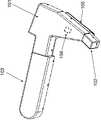
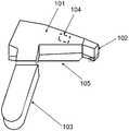
- Figs. 1a-1billustrate one exemplary fall-proof apparatus for cleaning semiconductor devices.
- Figs. 2a-2billustrate a bottom section view of one exemplary fall-proof apparatus for cleaning semiconductor devices.
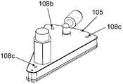
- Fig. 3illustrates one exemplary megasonic/ultrasonic device of the fall-proof apparatus for cleaning semiconductor devices.
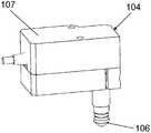
- Fig. 4illustrates one exemplary sensor of the fall-proof apparatus for cleaning semiconductor devices.
- Figs. 5a-5billustrate one exemplary chamber of the present invention.
- Fig. 6illustrates one exemplary tray of the chamber.
- Fig. 7illustrates one exemplary fall-proof apparatus for cleaning semiconductor devices of the chamber.
- Fig. 8illustrates one exemplary megasonic/ultrasonic device of the chamber.
- Fig. 9illustrates one exemplary sensor of the chamber.
- Figs. 1a-1billustrate one exemplary fall-proof apparatus for cleaning semiconductor devices.
- the fall-proof apparatus for cleaning semiconductor devicescomprises a nozzle 102 connecting with a carrier 101; a megasonic/ultrasonic device 105 fixing on the carrier 101, the megasonic/ultrasonic device 105 working with the nozzle 102 during a cleaning process; a sensor 104 detecting the distance between the megasonic/ultrasonic device 105 and the carrier 101 to make a judgment on whether the megasonic/ultrasonic device 105 is loose and going to fall.
- the fall-proof apparatuscomprises a swing arm 103 driving the fall-proof apparatus to move.
- Figs. 2a-2billustrate a bottom section view of one exemplary fall-proof apparatus for cleaning semiconductor devices.
- the megasonic/ultrasonic device 105is fan-shaped, so adaptable to a round semiconductor device.
- Fig 2bone exemplary fall-proof apparatus for cleaning semiconductor devices is shown, the megasonic/ultrasonic device 105 of this fall-proof apparatus is removed. So it can be seen that the sensor 104 is fixed on the carrier 101, and is placed between the megasonic/ultrasonic device and the carrier 101.
- an output of the sensorsuch as a sensor reading is in proportion to the distance between the megasonic/ultrasonic device 105 and the carrier 101. Further, if the distance between the megasonic/ultrasonic device 105 and the carrier 101 is a minimum, the output of the sensor, such as the sensor reading is “0” . In one embodiment, the sensor 104 has an accuracy of 0.01mm or a higher accuracy.
- the fall-proof apparatusfurther comprises an automatic alarm connecting with the sensor 104.
- the automatic alarmwill be triggered if the sensor reading exceeds a preset threshold, which can remind the operating personnel to fix the megasonic/ultrasonic device 105.
- the megasonic/ultrasonic device 105will have a lower chance of falling to break the semiconductor device below.
- Fig. 3illustrates one exemplary megasonic/ultrasonic device of the fall-proof apparatus for cleaning semiconductor devices.
- the megasonic/ultrasonic device 105is fixed on the bottom side of the carrier 101 by at least one pair of screws and nuts which can adjust the distance between the megasonic/ultrasonic device 105 and the carrier 101.
- the sensor 104is used to detect a position change of the megasonic/ultrasonic device 105 caused by loss of the screws and nuts 108. Loss of a part of all of the three pairs of screws and nuts may cause a position change of the megasonic/ultrasonic device 105.
- the sensor 104detects a distance between the megasonic/ultrasonic device 105 and the carrier 101, the distance is represented by the output of the sensor 104 and is used as a reference for adjusting the screws and nuts. That is, at least one pair of the srews and nuts are loosed or tightened according to the output of the sensor. Further, in the cleaning process, cleaning liquid flows out from the nozzle 102 to the semiconductor device, the megasonic/ultrasonic device 105 is immerged into the cleaning liquid and used for generating megasonic/ultrasonic waves.
- Fig. 4illustrates one exemplary sensor of the fall-proof apparatus for cleaning semiconductor devices.
- the sensor 104is a pressure sensor comprising a measuring end 106 and a fixing end 107, the fixing end 107 is fixed on the carrier 101, the measuring end 106 is retractable and pressed tightly by the megasonic/ultrasonic device 105.
- the pressure sensordetects the expansion amount of the measuring end 106 to make a judgment on whether the megasonic/ultrasonic device 105 becoming loose and fall.
- the senor 104is a light sensor.
- the light sensoremits light signal toward the megasonic/ultrasonic device 105 and receives the reflected light signal to calculate the time taken for this round-trip of light signal. By this means, the distance between the carrier 101 and the megasonic/ultrasonic device 105 can be detected.
- the senor 104is an electric sensor.
- the electric sensorcan detect the distance between the carrier 101 and the megasonic/ultrasonic device 105 by monitoring the variation of electrical parameters.
- a chamber of the present inventionis provided.
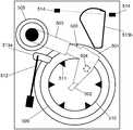
- Figs. 5a-5billustrate one exemplary chamber of the present invention.
- the chambercomprises a fall-proof apparatus 500 for cleaning semiconductor devices
- the fall-proof apparatus 500comprises a nozzle 502 connecting with a carrier 501, a megasonic/ultrasonic device 505 fixing on the carrier 501, the megasonic/ultrasonic device 505 working with the nozzle 502 during a cleaning process, a sensor 504 detecting the distance between the megasonic/ultrasonic device 505 and the carrier 501 to make a judgment on whether the megasonic/ultrasonic device 505 becoming loose and fall; a chuck 509 for holding and rotating the semiconductor devices 510; a swing-spray head 512 swinging back and forth above the semiconductor devices 510 and spraying chemical liquid or gas to clean the semiconductor devices 510; and at least two trays 513 for flushing or cleaning the swing-spray head 512 or the megasonic/ultrasonic device 505.
- the fall-proof apparatus 500further comprises a swing arm 503 and a vertical actuator 508.
- the swing arm 503driving the fall-proof apparatus 500 to move.
- the vertical actuator 508driving the fall-proof apparatus 500 to move up and down.
- the chuck 509driving the semiconductor device 510 to rotate during the cleaning process.
- some clamping elements 511are distributed on the chuck 509 and around the semiconductor device 510 for preventing the semiconductor device 510 from moving.
- the swing-spray head 512swinging back and forth within a working position which is above the semiconductor device 510, to spray chemical liquids onto the semiconductor device 510 first.
- the swing-spray head 512is driven to the idle position, while the megasonic/ultrasonic device 505 is driven to the working position.
- the nozzle 502keeps on spraying chemical liquids onto the semiconductor device 510 at the working position, and the the megasonic/ultrasonic device 505 is driven down by the vertical actuator 508 and immerged into the chemical liquids to generate megasonic/ultrasonic waves for cleaning the semiconductor device 505.
- the megasonic/ultrasonic wavespropagate and vibrate in the chemical liquids, Meanwhile, the chuck 509 driving the semiconductor device 510 to rotate during the cleaning process. By this means, the semiconductor device 510 can be cleaned in the cleaning process.
- Fig. 5ait can be seen that the megasonic/ultrasonic device 505 is working, while the swing-spray head 512 is staying at the second idle position, keeping the swing-spray head 512 above the tray 513a.
- Fig. 5bit can be seen that the swing-spray head 512 is working, while the swing arm 503 is staying at a first idle position, keeping the megasonic/ultrasonic device 505 above the tray 513b.
- the shapes of the at least two trays 513, tray 513a and tray 513b,can be different from each other to match the swing-spray head 512 and the megasonic/ultrasonic device 505.
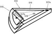
- a tray 513 of the present chamberis given.
- the tray 513comprises an inner tray 516 and an outer tray 515, the inner tray 516 is arranged inside the outer tray 515 and has a lower sidewall than the outer tray 515. Both the inner tray 516 and the outer tray 517 have a drain outlet 517 respectively. Further, the tray 513 has an ejection head 518 for flushing or cleaning the swing-spray head 512 or the megasonic/ultrasonic device 505 by liquid ejection.
- the swing-spray head 512 and the megasonic/ultrasonic device 505need to be flushed before starting the cleaning process. Because the chemical liquids sprayed from the swing-spray head 512 and the nozzle 502 may not meet the process requirement at the beginning of the cleaning process. Some technical parameters, such as temperature, flow rate, etc, are not very stable, so it is necessary to flush the swing-spray head 512 and the megasonic/ultrasonic device 505 before starting the cleaning process.
- the swing-spray head 512 or the megasonic/ultrasonic device 505is driven to the top of one tray 513, spraying chemical liquids into the tray 513 for a period of time. Further, the nozzle 502 and the swing-spray head 512 are connected to a monitoring system to detect the relative technical parameters. The swing-spray head 512 and the megasonic/ultrasonic device 505 will be driven back to the working position until the chemical liquids meet the process requirement.
- the distance between the megasonci/ultrasonic device 505 and the semiconductor device 510will be too close during the cleaning process, which may break the semiconductor devices 510.
- at least a pair of transducers 514are horizontally disposed on both sides of the tray 513b to detect whether the swing arm 503 is bending by sending and receiving light signals.
- the transducers 514are laser transducers. After the swing arm 503 gets back to the idle position, if the at least a pair of transducers 514 can not receive the light signals, which means the swing arm 503 is bending and need to be replaced or repaired. Otherwise, if the at least a pair of transducers 514 can receive the light signals as normal, which means the swing arm 503 is horizontal.
- the swing-spray head 512 or the megasonic/ultrasonic device 505is also driven to the top of one tray 513 during idle time.
- the ejection head 518sprays cleaning liquid toward the swing-spray head 512 or the megasonic/ultrasonic device 505 for cleaning the swing-spray head 512 or the megasonic/ultrasonic device 505.
- the megasonic/ultrasonic device 505 driven by the vertical actuator 508moves down and immerges into the cleaning liquid. So the particles and contaminants will be removed by this liquid ejection.
- the cleaning liquidis DIW. Referring to Fig.
- the ejection head 518is in the inner tray 516, and the inner tray 516 has a lower sidewall than the outer tray 515. So if the inner tray 516 is filled up with cleaning liquid, the excess cleaning liquid will spill out into the outer tray 515. By this means, the cleaning liquid in the inner tray 516 is kept clean and running, which is conductive to cleaning the swing-spray head 512 or the megasonic/ultrasonic device 505. Further, both the inner tray 516 and the outer tray 515 have a drain outlet 517 for draining out the cleaning liquid respectively.
- Fig. 7illustrates one exemplary fall-proof apparatus for cleaning semiconductor devices of the chamber.
- the fall-proof apparatus for cleaning semiconductor devicescomprises a nozzle 502 connecting with a carrier 501; a megasonic/ultrasonic device 505 fixing on the carrier 501, the megasonic/ultrasonic device 505 working with the nozzle 502 during a cleaning process; a sensor 504 detecting the distance between the megasonic/ultrasonic device 505 and the carrier 501 to make a judgment on whether the megasonic/ultrasonic device 505 becoming loose and fall.
- the fall-proof apparatuscomprises a swing arm 503 driving the fall-proof apparatus to move.
- the megasonic/ultrasonic device 505is fan-shaped, so adaptable to a round semiconductor device 510.
- the sensor 504is fixed on the carrier 501, and is placed between the megasonic/ultrasonic device and the carrier 501.
- an output of the sensorsuch as a sensor reading is in proportion to the distance between the megasonic/ultrasonic device 505 and the carrier 501. Further, if the distance between the megasonic/ultrasonic device 505 and the carrier 501 is a minimum, the output of the sensor, such as the sensor reading is “0” . In one embodiment, the sensor 504 has an accuracy of 0.01mm or a higher accuracy.
- the fall-proof apparatusfurther comprises an automatic alarm connecting with the sensor 504.
- the automatic alarmwill be triggered if the output of the sensor, such as the sensor reading exceeds a preset threshold, which can remind the operating personnel to fix the megasonic/ultrasonic device 505.
- the megasonic/ultrasonic device 505will have a lower chance of falling to break the semiconductor device 510 below.
- Fig. 8illustrates one exemplary megasonic/ultrasonic device of the chamber.
- the megasonic/ultrasonic device 505is fixed on the bottom side of the carrier 501 by at least a pair of screws and nuts which can adjust the distance between the megasonic/ultrasonic device and the carrier.
- the sensor 104is used to detect a position change of the megasonic/ultrasonic device 105 caused by loss of the screws and nuts 519. Loss of a part of all of the three pairs of screws and nuts may cause a position change of the megasonic/ultrasonic device 505.
- the sensor 504detects a distance between the megasonic/ultrasonic device 505 and the carrier 501, the distance is represented by the output of the sensor 504 and is used as a reference for adjusting the screws and nuts. That is, at least one pair of the srews and nuts are loosed or tightened according to the output of the sensor. Further, in the cleaning process, cleaning liquid flows out from the nozzle 502 to the semiconductor device, the megasonic/ultrasonic device 505 is immerged into the cleaning liquid and used for generating megasonic/ultrasonic waves.
- Fig. 9illustrates one exemplary sensor of the chamber.
- the sensor 504is a pressure sensor comprising a measuring end 506 and a fixing end 507, the fixing end 507 is fixed on the carrier 501, the measuring end 506 is retractable and pressed tightly by the megasonic/ultrasonic device 505.
- the pressure sensordetects the expansion amount of the measuring end 506 to make a judgment on whether the megasonic/ultrasonic device 505 becoming loose and fall.
- the senor 504is a light sensor.
- the light sensoremits light signal toward the megasonic/ultrasonic device 505 and receives the reflected light signal to calculate the time taken for this round-trip of light signal. By this means, the distance between the carrier 501 and the megasonic/ultrasonic device 505 can be detected.
- the senor 504is an electric sensor.
- the electric sensorcan detect the distance between the carrier 501 and the megasonic/ultrasonic device 505 by monitoring the variation of electrical parameters.
Landscapes
- Engineering & Computer Science (AREA)
- General Physics & Mathematics (AREA)
- Physics & Mathematics (AREA)
- Power Engineering (AREA)
- Condensed Matter Physics & Semiconductors (AREA)
- Manufacturing & Machinery (AREA)
- Computer Hardware Design (AREA)
- Microelectronics & Electronic Packaging (AREA)
- Mechanical Engineering (AREA)
- Business, Economics & Management (AREA)
- Emergency Management (AREA)
- Chemical & Material Sciences (AREA)
- Chemical Kinetics & Catalysis (AREA)
- General Chemical & Material Sciences (AREA)
- Cleaning Or Drying Semiconductors (AREA)
- Cleaning By Liquid Or Steam (AREA)
Abstract
Description
The present invention generally relates to a fall-proof apparatus and a chamber with the fall-proof apparatus. More particularly, it relates to a fall-proof apparatus for cleaning semiconductor devices by applying megasonic/ultrasonic energy onto semiconductor devices.
With the development of science and technology, the semiconductor cleaning process is maturing day by day. Differing from the traditional mechanical cleaning process, a large number of advanced high-tech cleaning apparatuses and equipment begin to make their presence felt in the semiconductor manufacturing and processing market. As one of the best, the apparatuses and equipment having a megasonic/ultrasonic device are highly recommended.
The megasonic/ultrasonic device is a key unit for the advanced high-tech cleaning apparatus and equipment. The megasonic/ultrasonic device always works with a nozzle. During the cleaning process, under the high frequency vibration effect and the chemical reaction, the molecules of cleaning liquid driven by the megasonic/ultrasonic waves successionally collide with the surface of the semiconductor device at a very high speed, by which the particles and tiny contaminants can be removed and resolved into the cleaning liquid.
As one of the key unit for the advanced high-tech cleaning apparatus and equipment, the megasonic/ultrasonic device could be large and heavy. Generally, the megasonic/ultrasonic device is fixed on an carrier, moving with the carrier inside the cleaning liquid. During the cleaning process, the megasonic/ultrasonic device is located above the semiconductor device, sending megasonic/ultrasonic waves towards the semiconductor device. Through a long period of usage, if the megasonic/ultrasonic device is not fixed firmly with the carrier, or the fixation between the megasonic/ultrasonic device and the carrier becomes loose, the megasonic/ultrasonic device will possibly fall off and break the semiconductor device below into pieces. Meanwhile, the megasonic/ultrasonic device keeps moving during the cleaning process, which increases the risk of the megasonic/ultrasonic device falling off. As is known to us, a semiconductor device costs thousands of dollars or even higher. So if this incident is not well controlled, it will become a great cost to the manufacturers and suppliers.
Moreover, after a long period of usage, particles and tiny contaminants may be generated on the megasonic/ultrasonic device or other units. So the megasonic/ultrasonic device need to be cleaned frequently in a chamber.
SUMMARY
According to an embodiment of the present invention, a fall-proof apparatus for cleaning semiconductor devices is provided. The fall-proof apparatus comprises: a nozzle connecting with a carrier; a megasonic device fixing on the carrier, the megasonic/ultrasonic device works with the nozzle during a cleaning process; a sensor detecting the distance between the megasonic/ultrasonic device and the carrier to determine whether the megasonic/ultrasonic device is loose and going to fall.
According to anther embodiment of the present invention, a chamber is provided. The chamber comprises: a fall-proof apparatus for cleaning semiconductor devices, the fall-proof apparatus comprises a nozzle connecting with a carrier, a megasonic/ultrasonic device fixing on the carrier, the megasonic/ultrasonic device works with nozzle during a cleaning process, a sensor detecting the distance between the megasonic/ultrasonic device and the carrier to determine whether the megasonic/ultrasonic device is loose and going to fall; a chuck for holding and rotating the semiconductor devices; a swing-spray head swinging back and forth above the semiconductor devices and spraying chemical liquid or gas to clean the semiconductor devices; and at least two trays for flushing or cleaning the swing-spray head or the megasonic/ultrasonic device.
The present invention provides a fall-proof apparatus for cleaning semiconductor devices. Moreover, a chamber with the fall-proof apparatus is also provided in the present invention. Other objects and features will become apparent from the following detailed description taken in connection with the accompanying drawings. However, the drawings are provided for purpose of illustration only, and are not intended as a definition of the limits of the invention.
Figs. 1a-1b illustrate one exemplary fall-proof apparatus for cleaning semiconductor devices.
Figs. 2a-2b illustrate a bottom section view of one exemplary fall-proof apparatus for cleaning semiconductor devices.
Fig. 3 illustrates one exemplary megasonic/ultrasonic device of the fall-proof apparatus for cleaning semiconductor devices.
Fig. 4 illustrates one exemplary sensor of the fall-proof apparatus for cleaning semiconductor devices.
Figs. 5a-5b illustrate one exemplary chamber of the present invention.
Fig. 6 illustrates one exemplary tray of the chamber.
Fig. 7 illustrates one exemplary fall-proof apparatus for cleaning semiconductor devices of the chamber.
Fig. 8 illustrates one exemplary megasonic/ultrasonic device of the chamber.
Fig. 9 illustrates one exemplary sensor of the chamber.
Preferred embodiments of this invention will be described in detail hereinafter with reference to the drawings. The embodiments of the present invention described are not limit the invention to the precise forms disclosed in the following detailed description.
Figs. 1a-1b illustrate one exemplary fall-proof apparatus for cleaning semiconductor devices. The fall-proof apparatus for cleaning semiconductor devices comprises a nozzle 102 connecting with a carrier 101; a megasonic/ultrasonic device 105 fixing on the carrier 101, the megasonic/ultrasonic device 105 working with the nozzle 102 during a cleaning process; a sensor 104 detecting the distance between the megasonic/ultrasonic device 105 and the carrier 101 to make a judgment on whether the megasonic/ultrasonic device 105 is loose and going to fall. Further more, the fall-proof apparatus comprises a swing arm 103 driving the fall-proof apparatus to move.
Figs. 2a-2b illustrate a bottom section view of one exemplary fall-proof apparatus for cleaning semiconductor devices. Referring to Fig 2a, it can be seen that the megasonic/ultrasonic device 105 is fan-shaped, so adaptable to a round semiconductor device. And referring to Fig 2b, one exemplary fall-proof apparatus for cleaning semiconductor devices is shown, the megasonic/ultrasonic device 105 of this fall-proof apparatus is removed. So it can be seen that the sensor 104 is fixed on the carrier 101, and is placed between the megasonic/ultrasonic device and the carrier 101.
In one embodiment of the present invention, an output of the sensor, such as a sensor reading is in proportion to the distance between the megasonic/ultrasonic device 105 and the carrier 101. Further, if the distance between the megasonic/ultrasonic device 105 and the carrier 101 is a minimum, the output of the sensor, such as the sensor reading is “0” . In one embodiment, the sensor 104 has an accuracy of 0.01mm or a higher accuracy.
In one embodiment, the fall-proof apparatus further comprises an automatic alarm connecting with the sensor 104. The automatic alarm will be triggered if the sensor reading exceeds a preset threshold, which can remind the operating personnel to fix the megasonic/ultrasonic device 105. By this means, the megasonic/ultrasonic device 105 will have a lower chance of falling to break the semiconductor device below.
Fig. 3 illustrates one exemplary megasonic/ultrasonic device of the fall-proof apparatus for cleaning semiconductor devices. In one embodiment, the megasonic/ultrasonic device 105 is fixed on the bottom side of the carrier 101 by at least one pair of screws and nuts which can adjust the distance between the megasonic/ultrasonic device 105 and the carrier 101. In one embodiment, there are three pairs of screws and nuts 108 distributed on the megasonic/ultrasonic device 105 in a triangular manner. The distance between the megasonic/ultrasonic device 105 and the carrier 101 can be adjusted by loosening or tightening at least one pair of the screws and nuts 108. The sensor 104 is used to detect a position change of the megasonic/ultrasonic device 105 caused by loss of the screws and nuts 108. Loss of a part of all of the three pairs of screws and nuts may cause a position change of the megasonic/ultrasonic device 105. The sensor 104 detects a distance between the megasonic/ultrasonic device 105 and the carrier 101, the distance is represented by the output of the sensor 104 and is used as a reference for adjusting the screws and nuts. That is, at least one pair of the srews and nuts are loosed or tightened according to the output of the sensor. Further, in the cleaning process, cleaning liquid flows out from the nozzle 102 to the semiconductor device, the megasonic/ultrasonic device 105 is immerged into the cleaning liquid and used for generating megasonic/ultrasonic waves.
Fig. 4 illustrates one exemplary sensor of the fall-proof apparatus for cleaning semiconductor devices. Referring to Fig. 4, in one embodiment, the sensor 104 is a pressure sensor comprising a measuring end 106 and a fixing end 107, the fixing end 107 is fixed on the carrier 101, the measuring end 106 is retractable and pressed tightly by the megasonic/ultrasonic device 105. The pressure sensor detects the expansion amount of the measuring end 106 to make a judgment on whether the megasonic/ultrasonic device 105 becoming loose and fall.
In another embodiment, the sensor 104 is a light sensor. The light sensor emits light signal toward the megasonic/ultrasonic device 105 and receives the reflected light signal to calculate the time taken for this round-trip of light signal. By this means, the distance between the carrier 101 and the megasonic/ultrasonic device 105 can be detected.
In one embodiment, the sensor 104 is an electric sensor. The electric sensor can detect the distance between the carrier 101 and the megasonic/ultrasonic device 105 by monitoring the variation of electrical parameters.
Referring to Fig. 5a-Fig. 9, a chamber of the present invention is provided.
Figs. 5a-5b illustrate one exemplary chamber of the present invention.
According to Figs. 5a-5b, the chamber comprises a fall-proof apparatus 500 for cleaning semiconductor devices, the fall-proof apparatus 500 comprises a nozzle 502 connecting with a carrier 501, a megasonic/ultrasonic device 505 fixing on the carrier 501, the megasonic/ultrasonic device 505 working with the nozzle 502 during a cleaning process, a sensor 504 detecting the distance between the megasonic/ultrasonic device 505 and the carrier 501 to make a judgment on whether the megasonic/ultrasonic device 505 becoming loose and fall; a chuck 509 for holding and rotating the semiconductor devices 510; a swing-spray head 512 swinging back and forth above the semiconductor devices 510 and spraying chemical liquid or gas to clean the semiconductor devices 510; and at least two trays 513 for flushing or cleaning the swing-spray head 512 or the megasonic/ultrasonic device 505. The fall-proof apparatus 500 further comprises a swing arm 503 and a vertical actuator 508. The swing arm 503 driving the fall-proof apparatus 500 to move. And the vertical actuator 508 driving the fall-proof apparatus 500 to move up and down. The chuck 509 driving the semiconductor device 510 to rotate during the cleaning process. And some clamping elements 511 are distributed on the chuck 509 and around the semiconductor device 510 for preventing the semiconductor device 510 from moving.
During the cleaning process, the swing-spray head 512 swinging back and forth within a working position which is above the semiconductor device 510, to spray chemical liquids onto the semiconductor device 510 first. After then, the swing-spray head 512 is driven to the idle position, while the megasonic/ultrasonic device 505 is driven to the working position. The nozzle 502 keeps on spraying chemical liquids onto the semiconductor device 510 at the working position, and the the megasonic/ultrasonic device 505 is driven down by the vertical actuator 508 and immerged into the chemical liquids to generate megasonic/ultrasonic waves for cleaning the semiconductor device 505. The megasonic/ultrasonic waves propagate and vibrate in the chemical liquids, Meanwhile, the chuck 509 driving the semiconductor device 510 to rotate during the cleaning process. By this means, the semiconductor device 510 can be cleaned in the cleaning process.
As is known to the skilled in this art, after a long period of usage, particles and tiny contaminants may be generated on the megasonic/ultrasonic device 505 and the nozzle 502. So the megasonic/ultrasonic device 505 and the nozzle 502 need to be cleaned frequently in a chamber during their idle time. Therefore, at least two trays 513 for flushing or cleaning the swing-spray head 512 or the megasonic/ultrasonic device 505 are provided in the chamber.
Referring to Fig. 5a, it can be seen that the megasonic/ultrasonic device 505 is working, while the swing-spray head 512 is staying at the second idle position, keeping the swing-spray head 512 above the tray 513a.
Referring to Fig. 5b, it can be seen that the swing-spray head 512 is working, while the swing arm 503 is staying at a first idle position, keeping the megasonic/ultrasonic device 505 above the tray 513b.
The shapes of the at least two trays 513, tray 513a and tray 513b, can be different from each other to match the swing-spray head 512 and the megasonic/ultrasonic device 505. Referring to Fig. 6, an exemplary tray 513 of the present chamber is given. The tray 513 comprises an inner tray 516 and an outer tray 515, the inner tray 516 is arranged inside the outer tray 515 and has a lower sidewall than the outer tray 515. Both the inner tray 516 and the outer tray 517 have a drain outlet 517 respectively. Further, the tray 513 has an ejection head 518 for flushing or cleaning the swing-spray head 512 or the megasonic/ultrasonic device 505 by liquid ejection.
In some cases, the swing-spray head 512 and the megasonic/ultrasonic device 505 need to be flushed before starting the cleaning process. Because the chemical liquids sprayed from the swing-spray head 512 and the nozzle 502 may not meet the process requirement at the beginning of the cleaning process. Some technical parameters, such as temperature, flow rate, etc, are not very stable, so it is necessary to flush the swing-spray head 512 and the megasonic/ultrasonic device 505 before starting the cleaning process.
For flushing the swing-spray head 512 and the megasonic/ultrasonic device 505, the swing-spray head 512 or the megasonic/ultrasonic device 505 is driven to the top of one tray 513, spraying chemical liquids into the tray 513 for a period of time. Further, the nozzle 502 and the swing-spray head 512 are connected to a monitoring system to detect the relative technical parameters. The swing-spray head 512 and the megasonic/ultrasonic device 505 will be driven back to the working position until the chemical liquids meet the process requirement. In some cases, if the swing arm 503 is bending, the distance between the megasonci/ultrasonic device 505 and the semiconductor device 510 will be too close during the cleaning process, which may break the semiconductor devices 510. So at least a pair of transducers 514 are horizontally disposed on both sides of the tray 513b to detect whether the swing arm 503 is bending by sending and receiving light signals. In one embodiment, the transducers 514 are laser transducers. After the swing arm 503 gets back to the idle position, if the at least a pair of transducers 514 can not receive the light signals, which means the swing arm 503 is bending and need to be replaced or repaired. Otherwise, if the at least a pair of transducers 514 can receive the light signals as normal, which means the swing arm 503 is horizontal.
For cleaning the swinig-spray head 512 and the megasonic/ultrasonic device 505, the swing-spray head 512 or the megasonic/ultrasonic device 505 is also driven to the top of one tray 513 during idle time. The ejection head 518 sprays cleaning liquid toward the swing-spray head 512 or the megasonic/ultrasonic device 505 for cleaning the swing-spray head 512 or the megasonic/ultrasonic device 505. And the megasonic/ultrasonic device 505 driven by the vertical actuator 508 moves down and immerges into the cleaning liquid. So the particles and contaminants will be removed by this liquid ejection. In one embodiment, the cleaning liquid is DIW. Referring to Fig. 6, it can be seen that the ejection head 518 is in the inner tray 516, and the inner tray 516 has a lower sidewall than the outer tray 515. So if the inner tray 516 is filled up with cleaning liquid, the excess cleaning liquid will spill out into the outer tray 515. By this means, the cleaning liquid in the inner tray 516 is kept clean and running, which is conductive to cleaning the swing-spray head 512 or the megasonic/ultrasonic device 505. Further, both the inner tray 516 and the outer tray 515 have a drain outlet 517 for draining out the cleaning liquid respectively.
Fig. 7 illustrates one exemplary fall-proof apparatus for cleaning semiconductor devices of the chamber. The fall-proof apparatus for cleaning semiconductor devices comprises a nozzle 502 connecting with a carrier 501; a megasonic/ultrasonic device 505 fixing on the carrier 501, the megasonic/ultrasonic device 505 working with the nozzle 502 during a cleaning process; a sensor 504 detecting the distance between the megasonic/ultrasonic device 505 and the carrier 501 to make a judgment on whether the megasonic/ultrasonic device 505 becoming loose and fall. Further more, the fall-proof apparatus comprises a swing arm 503 driving the fall-proof apparatus to move. In one embodiment, the megasonic/ultrasonic device 505 is fan-shaped, so adaptable to a round semiconductor device 510. The sensor 504 is fixed on the carrier 501, and is placed between the megasonic/ultrasonic device and the carrier 501.
In one embodiment of the present invention, an output of the sensor, such as a sensor reading is in proportion to the distance between the megasonic/ultrasonic device 505 and the carrier 501. Further, if the distance between the megasonic/ultrasonic device 505 and the carrier 501 is a minimum, the output of the sensor, such as the sensor reading is “0” . In one embodiment, the sensor 504 has an accuracy of 0.01mm or a higher accuracy.
In one embodiment, the fall-proof apparatus further comprises an automatic alarm connecting with the sensor 504. The automatic alarm will be triggered if the output of the sensor, such as the sensor reading exceeds a preset threshold, which can remind the operating personnel to fix the megasonic/ultrasonic device 505. By this means, the megasonic/ultrasonic device 505 will have a lower chance of falling to break the semiconductor device 510 below.
Fig. 8 illustrates one exemplary megasonic/ultrasonic device of the chamber. In one embodiment, the megasonic/ultrasonic device 505 is fixed on the bottom side of the carrier 501 by at least a pair of screws and nuts which can adjust the distance between the megasonic/ultrasonic device and the carrier. In one embodiment, there are three pairs of screws and nuts 519 distributed on the megasonic/ultrasonic device 505 in a triangular manner. The distance between the megasonic/ultrasonic device 505 and the carrier 501 can be adjusted by loosening or tightening at least one pair of the screws and nuts 519. The sensor 104 is used to detect a position change of the megasonic/ultrasonic device 105 caused by loss of the screws and nuts 519. Loss of a part of all of the three pairs of screws and nuts may cause a position change of the megasonic/ultrasonic device 505. The sensor 504 detects a distance between the megasonic/ultrasonic device 505 and the carrier 501, the distance is represented by the output of the sensor 504 and is used as a reference for adjusting the screws and nuts. That is, at least one pair of the srews and nuts are loosed or tightened according to the output of the sensor. Further, in the cleaning process, cleaning liquid flows out from the nozzle 502 to the semiconductor device, the megasonic/ultrasonic device 505 is immerged into the cleaning liquid and used for generating megasonic/ultrasonic waves.
Fig. 9 illustrates one exemplary sensor of the chamber. Referring to Fig. 9, in one embodiment, the sensor 504 is a pressure sensor comprising a measuring end 506 and a fixing end 507, the fixing end 507 is fixed on the carrier 501, the measuring end 506 is retractable and pressed tightly by the megasonic/ultrasonic device 505. The pressure sensor detects the expansion amount of the measuring end 506 to make a judgment on whether the megasonic/ultrasonic device 505 becoming loose and fall.
In another embodiment, the sensor 504 is a light sensor. The light sensor emits light signal toward the megasonic/ultrasonic device 505 and receives the reflected light signal to calculate the time taken for this round-trip of light signal. By this means, the distance between the carrier 501 and the megasonic/ultrasonic device 505 can be detected.
In one embodiment, the sensor 504 is an electric sensor. The electric sensor can detect the distance between the carrier 501 and the megasonic/ultrasonic device 505 by monitoring the variation of electrical parameters.
Although the present invention has been described with respect to certain embodiments, examples, and applications, it will be apparent to those skilled in the art that various modifications and changes may be made without departing from the invention.
Claims (26)
- A fall-proof apparatus for cleaning semiconductor devices, comprising:a nozzle connecting with a carrier;a megasonic/ultrasonic device fixing on the carrier, the megasonic/ultrasonic device working with the nozzle during a cleaning process;a sensor detecting the distance between the megasonic/ultrasonic device and the carrier to determine whether the megasonic/ultrasonic device is loose and going to fall.
- The fall-proof apparatus of claim 1, wherein the megasonic/ultrasonic device is fixed on the carrier by at least one pair of screws and nuts, and the distance between the megasonic/ultrasonic device and the carrier is adjusted by loosening or tightening the at least one pair of the screws and nuts.
- The fall-proof apparatus of claim 1, wherein the sensor is one of the following:a pressure sensor, a light sensor or an electric sensor.
- The fall-proof apparatus of claim 1, wherein the an output of the sensor is in proportion to the distance between the megasonic/ultrasonic device and the carrier.
- The fall-proof apparatus of claim 4, wherein the output of the sensor is a sensor reading and the sensor reading is “0” if the distance between the megasonic/ultrasonic device is a minimum.
- The fall-proof apparatus of claim 1, wherein the sensor has an accuracy of 0.01mm or a higher accuracy.
- The fall-proof apparatus of claim 1, wherein the fall-proof apparatus further comprising an automatic alarm connecting with the sensor.
- The fall-proof apparatus of claim 7, wherein the automatic alarm is triggered if an output of the sensor exceeds a preset threshold.
- The fall-proof apparatus of claim 1, wherein the fall-proof apparatus further comprising a swing arm driving the fall-proof apparatus to move.
- A chamber, comprising:a fall-proof apparatus for cleaning semiconductor devices, the fall-proof apparatus comprising a nozzle connecting with a carrier, a megasonic/ultrasonic device fixing on the carrier, the megasonic/ultrasonic device working with the nozzle during a cleaning process, a sensor detecting the distance between the megasonic/ultrasonic device and the carrier to determine whether the megasonic/ultrasonic device is loose and going to fall;a chuck for holding and rotating the semiconductor devices;a swing-spray head swinging back and forth above the semiconductor devices and spraying chemical liquid or gas to clean the semiconductor devices; andat least two trays for flushing or cleaning the swing-spray head or the megasonic/ultrasonic device.
- The chamber of claim 10, wherein the megasonic/ultrasonic device is fixed on the carrier by at least one pair of screws and nuts, and the distance between the megasonic/ultrasonic device and the carrier is adjusted by loosening or tightening the at least one pair of the screws and nuts.
- The chamber of claim 10, wherein the sensor is one of the following:a pressure sensor, a light sensor or an electric sensor.
- The chamber of claim 10, wherein an output of the sensor is in proportion to the distance between the megasonic/ultrasonic device and the carrier.
- The chamber of claim 13, wherein the output of the sensor is a sensor reading and the sensor reading is “0” if the distance between the megasonic/ultrasonic device is a minimum.
- The chamber of claim 10, wherein the fall-proof apparatus further comprising a swing arm driving the fall-proof apparatus to move.
- The chamber of claim 15, wherein the swing arm staying at a first idle position during idle time, keeping the megasonic/ultrasonic device above one of the at least two trays.
- The chamber of claim 10, wherein the swing-spray head staying at a second idle position during idle time, keeping the swing-spray head above one of the at least two trays.
- The chamber of claim 10, wherein each of the at least two trays comprising an inner tray and an outer tray, the inner tray is arranged inside the outer tray and has a lower sidewall than the outer tray.
- The chamber of claim 18, wherein both the inner tray and the outer tray having a drain outlet respectively.
- The chamber of claim 10, wherein each of the at least two trays having a ejection head for flushing or cleaning the swing-spray head or the megasonic/ultrasonic device by liquid ejection.
- The chamber of claim 10, wherein the fall-proof apparatus further comprising a vertical actuator driving the fall-proof apparatus to move up and down.
- The chamber of claim 10, wherein the sensor has an accuracy of 0.01mm or a higher accuracy.
- The chamber of claim 10, wherein the fall-proof apparatus further comprising an automatic alarm connecting with the sensor.
- The chamber of claim 23, wherein the automatic alarm is triggered if an output of the sensor exceeds a preset threshold.
- The chamber of claim 10, wherein the nozzle and the spring-spray head are connected to a monitoring system to detect relative technical parameters.
- The chamber of claim 14, wherein the chamber further comprising at least a pair of transducers to detect whether the swing arm is bending.
Priority Applications (5)
| Application Number | Priority Date | Filing Date | Title |
|---|---|---|---|
| SG11201706200UASG11201706200UA (en) | 2015-02-15 | 2015-09-08 | A fall-proof apparatus for cleaning semiconductor devices and a chamber with the apparatus |
| CN201580075716.0ACN107210208B (en) | 2015-02-15 | 2015-09-08 | Anti-falling semiconductor device cleaning device and process chamber with same |
| US15/550,971US10770315B2 (en) | 2015-02-15 | 2015-09-08 | Fall-proof apparatus for cleaning semiconductor devices and a chamber with the apparatus |
| KR1020177023766AKR102382343B1 (en) | 2015-02-15 | 2015-09-08 | A fall-proof apparatus for cleaning semiconductor devices and a chamber with the apparatus |
| JP2017542071AJP6591555B2 (en) | 2015-02-15 | 2015-09-08 | Semiconductor device cleaning apparatus having fall prevention function, and chamber including the apparatus |
Applications Claiming Priority (2)
| Application Number | Priority Date | Filing Date | Title |
|---|---|---|---|
| CN201510081989.8ACN105983552B (en) | 2015-02-15 | 2015-02-15 | Anti-falling semiconductor cleaning device |
| CN201510081989.8 | 2015-02-15 |
Publications (1)
| Publication Number | Publication Date |
|---|---|
| WO2016127635A1true WO2016127635A1 (en) | 2016-08-18 |
Family
ID=56615285
Family Applications (1)
| Application Number | Title | Priority Date | Filing Date |
|---|---|---|---|
| PCT/CN2015/089096CeasedWO2016127635A1 (en) | 2015-02-15 | 2015-09-08 | A fall-proof apparatus for cleaning semiconductor devices and a chamber with the apparatus |
Country Status (6)
| Country | Link |
|---|---|
| US (1) | US10770315B2 (en) |
| JP (1) | JP6591555B2 (en) |
| KR (1) | KR102382343B1 (en) |
| CN (2) | CN105983552B (en) |
| SG (1) | SG11201706200UA (en) |
| WO (1) | WO2016127635A1 (en) |
Cited By (1)
| Publication number | Priority date | Publication date | Assignee | Title |
|---|---|---|---|---|
| CN109158236A (en)* | 2018-08-20 | 2019-01-08 | 华电电力科学研究院有限公司 | A kind of cleaning of steam power plant's combustion engine compressor high-pressure nozzle and cleaning method |
Families Citing this family (3)
| Publication number | Priority date | Publication date | Assignee | Title |
|---|---|---|---|---|
| KR102753342B1 (en)* | 2019-11-01 | 2025-01-14 | 에이씨엠 리서치 (상하이), 인코포레이티드 | Substrate cleaning method and device |
| US20250183059A1 (en)* | 2022-06-23 | 2025-06-05 | Acm Research (Shanghai), Inc. | Substrate processing apparatus |
| CN118293767B (en)* | 2024-06-06 | 2024-08-23 | 南安市装备制造业技术研究院 | Town road traffic measuring tool |
Citations (9)
| Publication number | Priority date | Publication date | Assignee | Title |
|---|---|---|---|---|
| US4064885A (en)* | 1976-10-26 | 1977-12-27 | Branson Ultrasonics Corporation | Apparatus for cleaning workpieces by ultrasonic energy |
| US5368054A (en)* | 1993-12-17 | 1994-11-29 | International Business Machines Corporation | Ultrasonic jet semiconductor wafer cleaning apparatus |
| US5980647A (en)* | 1997-07-15 | 1999-11-09 | International Business Machines Corporation | Metal removal cleaning process and apparatus |
| JP2001334221A (en)* | 2000-05-26 | 2001-12-04 | Dainippon Screen Mfg Co Ltd | Substrate cleaning apparatus |
| US6539952B2 (en)* | 2000-04-25 | 2003-04-01 | Solid State Equipment Corp. | Megasonic treatment apparatus |
| US6848455B1 (en)* | 2002-04-22 | 2005-02-01 | Novellus Systems, Inc. | Method and apparatus for removing photoresist and post-etch residue from semiconductor substrates by in-situ generation of oxidizing species |
| CN101516534A (en)* | 2006-10-20 | 2009-08-26 | 韩国机械研究院 | Megasonic cleaning module |
| KR20100005571A (en)* | 2008-07-07 | 2010-01-15 | 세메스 주식회사 | Pad conditioning unit, single type substrate polishing apparatus using the same, and pad conditioning method |
| WO2010111826A1 (en)* | 2009-03-31 | 2010-10-07 | Acm Research (Shanghai) Inc. | Methods and apparatus for cleaning semiconductor wafers |
Family Cites Families (27)
| Publication number | Priority date | Publication date | Assignee | Title |
|---|---|---|---|---|
| US4326553A (en)* | 1980-08-28 | 1982-04-27 | Rca Corporation | Megasonic jet cleaner apparatus |
| US5745946A (en)* | 1994-07-15 | 1998-05-05 | Ontrak Systems, Inc. | Substrate processing system |
| US5950643A (en)* | 1995-09-06 | 1999-09-14 | Miyazaki; Takeshiro | Wafer processing system |
| US6260562B1 (en)* | 1997-10-20 | 2001-07-17 | Dainippon Screen Mfg. Co., Ltd. | Substrate cleaning apparatus and method |
| JP3333733B2 (en)* | 1998-02-20 | 2002-10-15 | 東京エレクトロン株式会社 | Cleaning equipment |
| JP2001044467A (en)* | 1999-07-29 | 2001-02-16 | Kanegafuchi Chem Ind Co Ltd | System for cleaning integrated thin film solar cell |
| US6495463B2 (en)* | 1999-09-28 | 2002-12-17 | Strasbaugh | Method for chemical mechanical polishing |
| US6730176B2 (en)* | 2001-07-09 | 2004-05-04 | Birol Kuyel | Single wafer megasonic cleaner method, system, and apparatus |
| US7185661B2 (en)* | 2002-05-06 | 2007-03-06 | Akrion Technologies, Inc. | Reciprocating megasonic probe |
| JP2003340386A (en)* | 2002-05-23 | 2003-12-02 | Toshiba Corp | Ultrasonic cleaning device and ultrasonic cleaning method |
| EP3203498A1 (en)* | 2004-06-09 | 2017-08-09 | Nikon Corporation | Exposure apparatus and device manufacturing method |
| US20070175502A1 (en)* | 2004-07-30 | 2007-08-02 | I.P. Foundry, Inc. | Apparatus and method for delivering acoustic energy through a liquid stream to a target object for disruptive surface cleaning or treating effects |
| WO2007085015A2 (en)* | 2006-01-20 | 2007-07-26 | Akrion Technologies, Inc. | Acoustic energy system, method and apparatus for processing flat articles |
| JP5132108B2 (en)* | 2006-02-02 | 2013-01-30 | 株式会社Sokudo | Substrate processing equipment |
| JP2007290111A (en)* | 2006-03-29 | 2007-11-08 | Ebara Corp | Polishing method and polishing apparatus |
| JP4700570B2 (en)* | 2006-07-14 | 2011-06-15 | 株式会社新川 | Bonding apparatus, bonding tool tip cleaning method and program |
| US8052797B2 (en)* | 2006-10-24 | 2011-11-08 | Asahi Glass Company, Limited | Method for removing foreign matter from substrate surface |
| US8327861B2 (en)* | 2006-12-19 | 2012-12-11 | Lam Research Corporation | Megasonic precision cleaning of semiconductor process equipment components and parts |
| TWI421933B (en)* | 2007-05-16 | 2014-01-01 | Lam Res Corp | Apparatus and method for ultrasonic wet treatment of plate-like articles |
| US7913561B2 (en)* | 2008-02-05 | 2011-03-29 | Olympus Medical Systems Corp. | Ultrasonic wave vibrating apparatus |
| EP2270838B1 (en)* | 2009-07-02 | 2019-06-12 | IMEC vzw | Method and apparatus for controlling optimal operation of acoustic cleaning |
| US9044794B2 (en)* | 2009-12-31 | 2015-06-02 | Lam Research Ag | Ultrasonic cleaning fluid, method and apparatus |
| US9721754B2 (en)* | 2011-04-26 | 2017-08-01 | Carl Zeiss Smt Gmbh | Method and apparatus for processing a substrate with a focused particle beam |
| CN202290654U (en)* | 2011-10-10 | 2012-07-04 | 北京七星华创电子股份有限公司 | Mega sonic cleaning head and mega sonic cleaning system comprising same |
| US9385020B2 (en)* | 2011-12-19 | 2016-07-05 | SCREEN Holdings Co., Ltd. | Substrate holding and rotating device, substrate treatment apparatus including the device, and substrate treatment method |
| US9821348B2 (en)* | 2013-10-22 | 2017-11-21 | Taiwan Semiconductor Manufacturing Company, Ltd. | Method and apparatus for water edge exposure and backside cleaning |
| JP6386769B2 (en)* | 2014-04-16 | 2018-09-05 | 株式会社荏原製作所 | Substrate drying apparatus, control program, and substrate drying method |
- 2015
- 2015-02-15CNCN201510081989.8Apatent/CN105983552B/enactiveActive
- 2015-09-08CNCN201580075716.0Apatent/CN107210208B/enactiveActive
- 2015-09-08WOPCT/CN2015/089096patent/WO2016127635A1/ennot_activeCeased
- 2015-09-08USUS15/550,971patent/US10770315B2/enactiveActive
- 2015-09-08SGSG11201706200UApatent/SG11201706200UA/enunknown
- 2015-09-08JPJP2017542071Apatent/JP6591555B2/enactiveActive
- 2015-09-08KRKR1020177023766Apatent/KR102382343B1/enactiveActive
Patent Citations (9)
| Publication number | Priority date | Publication date | Assignee | Title |
|---|---|---|---|---|
| US4064885A (en)* | 1976-10-26 | 1977-12-27 | Branson Ultrasonics Corporation | Apparatus for cleaning workpieces by ultrasonic energy |
| US5368054A (en)* | 1993-12-17 | 1994-11-29 | International Business Machines Corporation | Ultrasonic jet semiconductor wafer cleaning apparatus |
| US5980647A (en)* | 1997-07-15 | 1999-11-09 | International Business Machines Corporation | Metal removal cleaning process and apparatus |
| US6539952B2 (en)* | 2000-04-25 | 2003-04-01 | Solid State Equipment Corp. | Megasonic treatment apparatus |
| JP2001334221A (en)* | 2000-05-26 | 2001-12-04 | Dainippon Screen Mfg Co Ltd | Substrate cleaning apparatus |
| US6848455B1 (en)* | 2002-04-22 | 2005-02-01 | Novellus Systems, Inc. | Method and apparatus for removing photoresist and post-etch residue from semiconductor substrates by in-situ generation of oxidizing species |
| CN101516534A (en)* | 2006-10-20 | 2009-08-26 | 韩国机械研究院 | Megasonic cleaning module |
| KR20100005571A (en)* | 2008-07-07 | 2010-01-15 | 세메스 주식회사 | Pad conditioning unit, single type substrate polishing apparatus using the same, and pad conditioning method |
| WO2010111826A1 (en)* | 2009-03-31 | 2010-10-07 | Acm Research (Shanghai) Inc. | Methods and apparatus for cleaning semiconductor wafers |
Cited By (2)
| Publication number | Priority date | Publication date | Assignee | Title |
|---|---|---|---|---|
| CN109158236A (en)* | 2018-08-20 | 2019-01-08 | 华电电力科学研究院有限公司 | A kind of cleaning of steam power plant's combustion engine compressor high-pressure nozzle and cleaning method |
| CN109158236B (en)* | 2018-08-20 | 2023-11-07 | 华电电力科学研究院有限公司 | A high-pressure nozzle and cleaning method for cleaning gas turbine compressors in thermal power plants |
Also Published As
| Publication number | Publication date |
|---|---|
| KR20170113595A (en) | 2017-10-12 |
| US20180033654A1 (en) | 2018-02-01 |
| US10770315B2 (en) | 2020-09-08 |
| CN105983552A (en) | 2016-10-05 |
| KR102382343B1 (en) | 2022-04-04 |
| CN105983552B (en) | 2019-12-24 |
| SG11201706200UA (en) | 2017-08-30 |
| JP6591555B2 (en) | 2019-10-16 |
| JP2018506858A (en) | 2018-03-08 |
| CN107210208A (en) | 2017-09-26 |
| CN107210208B (en) | 2020-05-19 |
Similar Documents
| Publication | Publication Date | Title |
|---|---|---|
| US10770315B2 (en) | Fall-proof apparatus for cleaning semiconductor devices and a chamber with the apparatus | |
| US11167325B2 (en) | Method for surface cleaning | |
| KR101384595B1 (en) | Ultrasonic cleaning apparatus and ultrasonic cleaning method | |
| JP5093699B2 (en) | Ultrasonic flaw detector at tube end | |
| KR102016684B1 (en) | Fouling reduction device and method | |
| KR101599214B1 (en) | Ultrasonic cleaning apparatus for large area | |
| WO2018082410A1 (en) | Water tank component and constant humidity machine | |
| CA3057902A1 (en) | Devices, systems, and methods for cleaning vessels | |
| US20010032657A1 (en) | Megasonic treatment apparatus | |
| KR20200061237A (en) | Method for cleaning semiconductor equipment and management system for semiconductor equipment | |
| US11554390B2 (en) | Ultrasonic/megasonic cleaning device | |
| KR101068807B1 (en) | Ultrasonic Cleaner for Water Quality Sensor | |
| WO2013024451A3 (en) | Methods and systems for removing contamination from a wire of a saw | |
| KR20190062526A (en) | Apparatus and method for cleaning semiconductor wafers | |
| US8911552B2 (en) | Use of acoustic waves for purging filters in semiconductor manufacturing equipment | |
| KR101688455B1 (en) | An ultrasonic transmitter having piezoelectric element capable of transverse prevention and ultrasonic cleaning device including the same | |
| KR20160001065U (en) | Device for measuring groove of chemical mechanical polishing pad and chemical mechanical polishing appartus including the same | |
| KR20150056287A (en) | Ultrasonic cleansing device for lcd pannel | |
| KR20160067575A (en) | Ultrasonic cleaning apparatus | |
| KR20160001066U (en) | Device for measuring groove of chemical mechanical polishing pad and chemical mechanical polishing appartus including the same | |
| JP3942420B2 (en) | Sound pressure monitor | |
| TW202519320A (en) | Bubble control system in liquid film, wafer cleaning equipment and wafer cleaning method | |
| KR20150038839A (en) | Painting pre-processing ultrasonic apparatus | |
| JP2022078147A (en) | Ultrasonic shower washing device | |
| JPH0393230A (en) | Ultrasonic cleaner and ultrasonic cleaning |
Legal Events
| Date | Code | Title | Description |
|---|---|---|---|
| 121 | Ep: the epo has been informed by wipo that ep was designated in this application | Ref document number:15881790 Country of ref document:EP Kind code of ref document:A1 | |
| WWE | Wipo information: entry into national phase | Ref document number:11201706200U Country of ref document:SG | |
| ENP | Entry into the national phase | Ref document number:2017542071 Country of ref document:JP Kind code of ref document:A | |
| NENP | Non-entry into the national phase | Ref country code:DE | |
| ENP | Entry into the national phase | Ref document number:20177023766 Country of ref document:KR Kind code of ref document:A | |
| 122 | Ep: pct application non-entry in european phase | Ref document number:15881790 Country of ref document:EP Kind code of ref document:A1 |