WO2016123810A1 - Capacitive touch screen and manufacturing method thereof - Google Patents
Capacitive touch screen and manufacturing method thereofDownload PDFInfo
- Publication number
- WO2016123810A1 WO2016123810A1PCT/CN2015/072453CN2015072453WWO2016123810A1WO 2016123810 A1WO2016123810 A1WO 2016123810A1CN 2015072453 WCN2015072453 WCN 2015072453WWO 2016123810 A1WO2016123810 A1WO 2016123810A1
- Authority
- WO
- WIPO (PCT)
- Prior art keywords
- conductive
- region
- substrate
- conductive layer
- touch screen
- Prior art date
- Legal status (The legal status is an assumption and is not a legal conclusion. Google has not performed a legal analysis and makes no representation as to the accuracy of the status listed.)
- Ceased
Links
Images


Classifications
- G—PHYSICS
- G06—COMPUTING OR CALCULATING; COUNTING
- G06F—ELECTRIC DIGITAL DATA PROCESSING
- G06F3/00—Input arrangements for transferring data to be processed into a form capable of being handled by the computer; Output arrangements for transferring data from processing unit to output unit, e.g. interface arrangements
- G06F3/01—Input arrangements or combined input and output arrangements for interaction between user and computer
- G06F3/03—Arrangements for converting the position or the displacement of a member into a coded form
- G06F3/041—Digitisers, e.g. for touch screens or touch pads, characterised by the transducing means
Definitions
- the present inventionrelates to a touch screen, and more particularly to a capacitive touch screen and a method of fabricating the same.
- the mainstream touch screenmainly comprises a protective cover, a glass or a film substrate, and a functional layer attached to the surface of the substrate for sensing the touch and connecting the outside, specifically comprising a sensing region formed in the middle of the surface of the substrate and having a shape formed at the edge of the substrate A lead area of multiple pins for connecting a Flexible Printed Circuit (FPC).
- FPCFlexible Printed Circuit
- the conductive materialis removed or not printed elsewhere on the substrate, that is, there is a gap between the lead regions, and the segmentation It is not easy to cause a short circuit.
- the laser processhas the advantages of simple process and less chemical pollution, so the application is also increasingly widespread.
- a conductive layeris first disposed on the substrate, and then the laser is irradiated around the desired pattern and the leads to form the sensing region and the lead region.
- unnecessary portions of the conductive layerare not completely removed, and the lead region is formed by cutting at one end away from the sensing region. When cutting, it is necessary to cut exactly at the end of the pin. However, in actual production, it is difficult to be completely accurate.
- the split positionis located at the end of the pin away from the side of the sensing area, a short circuit occurs between the pins due to the unremoved conductive portion; if it is biased toward the side of the sensing area, the edge of the substrate may be deformed after being divided, especially It is a film substrate.
- the pitch of adjacent pinsis relatively small, adjacent pins are likely to be short-circuited due to deformation of the substrate. Therefore, any situation will reduce the yield.
- Embodiments of the present inventionprovide a capacitive touch screen that can solve the above technical problems and a method of fabricating the same.
- a capacitive touch screenincludes a substrate and a conductive layer disposed on the substrate, the conductive layer including a sensing region in the middle and a lead region at the edge.
- the lead regionincludes an inner side adjacent to the sensing region, an outer side away from the sensing region, and a first side and a second side connecting the opposite sides of the inner and outer sides, the lead region further including an outer side extending from the inner side to the outer side Pin.
- the lead regionfurther includes a non-conductive region extending from the first side to the second side between the inner side and the outer side, the non-conductive region intersecting each of the pins.
- a method of fabricating a capacitive touch screencomprising: providing a substrate; disposing a conductive layer on the substrate; forming a sensing region in the middle of the conductive layer; and a lead region at an edge of the conductive layer; wherein the lead region includes An inner side of the sensing region, an outer side away from the sensing region, and a first side and a second side connecting the opposite inner and outer sides, the lead region further including a pin extending from the inner side to the outer side; A non-conductive region extending from the first side to the second side is formed between the inner side and the outer side of the region, the non-conductive region intersecting each of the leads; and the conductive layer and the substrate are divided along an outer side of the lead region.
- FIG. 1is a flow chart of a method of fabricating a capacitive touch screen according to a first embodiment of the present invention.
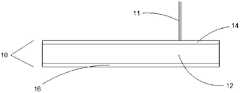
- FIG. 2is a side view showing the laser light irradiated on a conductive layer provided on a substrate according to the manufacturing method of FIG. 1.
- FIG. 3is a plan view of a capacitive touch screen fabricated in accordance with the method of FIG. 1.
- FIG. 4is a microscopic view showing a portion irradiated with and not irradiated in a partial region of the nanosilver film of FIG. 1.
- FIG. 5is an enlarged schematic view of a portion of a sensing region and a lead region on the capacitive touch screen of FIG. 3, in accordance with a first embodiment of the present invention.
- FIG. 6is an enlarged schematic view showing a portion of a sensing area and a lead area on a capacitive touch screen according to a second embodiment of the present invention.
- FIG. 7is an enlarged schematic view showing a portion of a sensing area and a lead area on a capacitive touch screen according to a third embodiment of the present invention.
- the present inventionprovides a capacitive touch screen and a method of fabricating the same.
- a method of manufacturing a capacitive touch screenwill be described first.
- the structure of the capacitive touch screenis also mentioned to better The manufacturing method is described. Therefore, the description of the structure of the capacitive touch screen is not separately described in the present specification.
- the structure of the capacitive touch screencan be clearly understood by those skilled in the art according to the description of the manufacturing method.
- FIG. 1 to FIG. 3are flowcharts of a method for fabricating a capacitive touch screen according to an embodiment of the present invention, including the following steps:
- the substrate 12can be made of a transparent material, such as glass or polyethylene terephthalate (PET), to facilitate the production of touch-enabled display screen modules or other applications requiring transparency.
- PETpolyethylene terephthalate
- the optional PETis used to fabricate the substrate 12, which has the advantages of good light transmission and flexibility, and is easy to manufacture.
- the substrate 12 made of PETmay have a thickness of about 0.01 to 0.5 millimeters (mm), preferably 0.015 to 0.2 mm, more preferably 0.1 mm, and the substrate in this thickness has a thickness. Good flexibility.
- the thickness of the substrate 12may be other options as well as other non-transparent materials, such as metals.
- Step S20A conductive layer 14 is provided on the substrate 12.
- the conductive layer 14may be a transparent conductive metal film having a nanometer dimension, including a film formed of a single metal, an alloy, a metal compound or any combination thereof in a nanometer dimension, such as a film including a nano wire, a film including a nano metal particle,
- the film including the nano metal meshmay of course be a graphene film, a carbon nanotube film, an organic conductive polymer film, an indium tin oxide (ITO) film or any combination thereof.
- the conductive layer 14is a transparent conductive nano-silver film, which is a film comprising a polymer matrix having nano-silver filaments, and the nano-silver filaments are uniformly distributed in the film to make the film transparent. And conductive features.
- the nanosilver filmcan be formed on the substrate 12 by coating, silk printing or spraying.
- the substrate 12 and the nanosilver film 14 disposed on one surface thereofconstitute the basic elements of the capacitive touch screen 10.
- the capacitive touch screen 10further includes a protective layer 16 on the side of the substrate 12 facing away from the conductive layer 14, and the protective layer 16 may be fixed to the substrate 12 by a scratch-resistant material such as a polycarbonate material or the like.
- Step S30forming a sensing region 20 located in the middle of the conductive layer 14 and a lead region 22 at the edge of the conductive layer 14.
- the sensing region 20 and the lead region 22are formed by a laser process. to make.
- adjusting the parameters of the laser light 11allows the laser light 11 to change the transparent conductive properties of the nanosilver film into a transparent and non-conductive manner without removing it.
- the laser parametersinclude pulse width, pulse flux, pulse energy, spot size, pulse repetition rate, and the like.
- the nanosilver in the irradiated portionwill change from conductive to non-conductive, and at the same time, the transparency of the irradiated portion hardly changes, and The exposed portion of the nanosilver film is hardly peeled off.
- conductive and non-conductiveis relative to the field of printed electronics, touch sensing or optoelectronics.
- a square resistance of about 30 to 250 ⁇ /sqcan be considered to be electrically conductive
- a square resistance of about 20 M ⁇ /sqcan be considered to be non-conductive.
- the conductive and non-conductivemay be differently defined, and the above laser parameters are set according to specific application scenarios.
- Fig. 4it is shown in an enlarged manner that the portion of the conductive layer 14 is partially irradiated with the laser irradiation portion 24 and the portions thereof which are not irradiated with laser light.
- the transparent characteristic and the conductive portion of the laser irradiated portion 24are slightly changed after being placed 200 times larger. Therefore, it is impossible to distinguish the portion irradiated by the laser by the naked eye without any magnification tool. 24 and the portion not irradiated with the laser, which is verified in the actual product, that is, the laser irradiated portion 24 after being irradiated by the laser 11 is also transparent.
- FIG. 5is an enlarged schematic view of a portion of the sensing region 20 and the lead region 22 on the capacitive touch screen of FIG.
- the sensing region 20has a pattern 26 for sensing a touch, and a row line 28 and a column line 29 drawn from the pattern 26, wherein the row line 28 and the column line 29 are both disposed on one side of the sensing region 20.
- the lead region 22includes an inner side 32 proximate the sensing region 20, an outer side 34 remote from the sensing region 20, and an oppositely disposed first side 36 and second side 38 connecting the inner side 32 and the outer side 34.
- the lead region 22has a plurality of pins 39 formed by laser irradiation lines, and the leads 39 are connected to corresponding row lines 28 and column lines 29.
- the pin 39extends from the inner side 32 to the outer side 34, and in the present embodiment Extends in a straight line.
- the laserilluminates the conductive layer from the outer side 34 to the inner side 32 from the lead region 22 and directly enters the sensing region 22 such that the lead 39 and its corresponding row line 28 or column line 29 are generated at a time.
- the laserilluminates the conductive layer from the outer side 34 to the inner side 32 from the lead region 22 and directly enters the sensing region 22 such that the lead 39 and its corresponding row line 28 or column line 29 are generated at a time.
- Step S40forming a non-conductive region 40 extending from the first side 36 to the second side 38 between the inner side 32 and the outer side 34 of the lead region 22.
- the non-conductive region 40is a portion in which the nanosilver film is transparent and non-conductive after being irradiated by the laser beam 11 without being removed. A portion of the non-conductive region 40 is shown in FIG. 5.
- the non-conductive region 40is a non-conductive line extending from the first side 36 to the second side 38 and intersects the pins and is perpendicular to each other.
- the non-conductive region 40is relatively close to the outer side 34 compared to the inner side 32, and the distance between the non-conductive region 40 and the outer side 34 is greater than the segmentation error.
- each pin 39can have a longer length to be connected to the FPC.
- the non-conductive region 40is not limited to a wire, and may have a larger width, such as a rectangle; in addition, the non-conductive region 40 may also extend from the first side 36 to the second side 38 with each pin 39.
- Step S50dividing the conductive layer 14 and the substrate 12 along the outer side 34 of the lead region 22.
- Step S50dividing the conductive layer 14 and the substrate 12 along the outer side 34 of the lead region 22.
- the present inventionsolves the problems described in the background art by the arrangement of the non-conductive regions 40, improving the yield yield.
Landscapes
- Engineering & Computer Science (AREA)
- General Engineering & Computer Science (AREA)
- Theoretical Computer Science (AREA)
- Human Computer Interaction (AREA)
- Physics & Mathematics (AREA)
- General Physics & Mathematics (AREA)
- Position Input By Displaying (AREA)
- Manufacturing Of Electric Cables (AREA)
- Switches That Are Operated By Magnetic Or Electric Fields (AREA)
Abstract
Description
Translated fromChinese本发明涉及触摸屏,尤其涉及电容触摸屏及其制造方法。The present invention relates to a touch screen, and more particularly to a capacitive touch screen and a method of fabricating the same.
目前主流的触摸屏主要包括保护盖板、玻璃或薄膜基板以及附设在基板表面的用于感测触摸及连接外部的功能层,具体包括在基板表面中部形成的感测区及在基板边缘形成的具有多个引脚的引线区,用于连接柔性电路板(Flexible Printed Circuit,FPC)。现有主流的制作工艺是,在基板上通过黄光光刻或丝网印刷的方式形成多个上述功能层,然后进行分割以得到多片触摸屏。在上述工艺下,除了感测区中的图案及引线区中的引脚外,在基板上的其它地方都是被去除或没有印刷上导电材料的,即是说引线区之间有间隙,分割时不易造成短路。At present, the mainstream touch screen mainly comprises a protective cover, a glass or a film substrate, and a functional layer attached to the surface of the substrate for sensing the touch and connecting the outside, specifically comprising a sensing region formed in the middle of the surface of the substrate and having a shape formed at the edge of the substrate A lead area of multiple pins for connecting a Flexible Printed Circuit (FPC). In the current mainstream manufacturing process, a plurality of the above functional layers are formed on the substrate by yellow lithography or screen printing, and then divided to obtain a plurality of touch screens. Under the above process, except for the pattern in the sensing region and the leads in the lead region, the conductive material is removed or not printed elsewhere on the substrate, that is, there is a gap between the lead regions, and the segmentation It is not easy to cause a short circuit.
相比上述主流工艺,镭射工艺具有制程简单及化学污染少的优点,因此应用也日益广泛。镭射工艺过程中,基板上先设置一导电层,再使激光在所需图案及引脚周围进行照射,从而形成上述感测区及引线区。在镭射工艺下,导电层不需要的部分不会被全部去除,引线区远离感测区一端通过切割的方式形成。切割时,需准确按照引脚的末端进行切割。然而,实际生产中,很难做到完全准确。若分割位置位于该引脚的末端偏向远离感测区一侧,引脚间会因未去除的导电部分而出现短路;若偏向靠近感测区一侧,由于分割后基板边缘会发生变形,尤其是薄膜基板,当相邻引脚的间距比较小的时候,相邻引脚容易由于基板的变形而出现短路。因此,任何一种情况都会降低制成良率。Compared with the above mainstream processes, the laser process has the advantages of simple process and less chemical pollution, so the application is also increasingly widespread. During the laser process, a conductive layer is first disposed on the substrate, and then the laser is irradiated around the desired pattern and the leads to form the sensing region and the lead region. Under the laser process, unnecessary portions of the conductive layer are not completely removed, and the lead region is formed by cutting at one end away from the sensing region. When cutting, it is necessary to cut exactly at the end of the pin. However, in actual production, it is difficult to be completely accurate. If the split position is located at the end of the pin away from the side of the sensing area, a short circuit occurs between the pins due to the unremoved conductive portion; if it is biased toward the side of the sensing area, the edge of the substrate may be deformed after being divided, especially It is a film substrate. When the pitch of adjacent pins is relatively small, adjacent pins are likely to be short-circuited due to deformation of the substrate. Therefore, any situation will reduce the yield.
发明内容Summary of the invention
本发明的实施方式提供了一种可解决上述技术问题的电容触摸屏及其制作方法。Embodiments of the present invention provide a capacitive touch screen that can solve the above technical problems and a method of fabricating the same.
一种电容触摸屏,包括一基材及设置于该基材的一导电层,该导电层包括位于中间的感测区及位于边缘的引线区。该引线区包括靠近该感测区的内侧、远离该感测区的外侧以及连接该内侧及外侧的相对设置的第一侧及第二侧,该引线区还包括自该内侧向该外侧延伸的引脚。该引线区还包括位于该内侧及外侧之间的自该第一侧向该第二侧延伸的非导电区,该非导电区与各引脚相交。A capacitive touch screen includes a substrate and a conductive layer disposed on the substrate, the conductive layer including a sensing region in the middle and a lead region at the edge. The lead region includes an inner side adjacent to the sensing region, an outer side away from the sensing region, and a first side and a second side connecting the opposite sides of the inner and outer sides, the lead region further including an outer side extending from the inner side to the outer side Pin. The lead region further includes a non-conductive region extending from the first side to the second side between the inner side and the outer side, the non-conductive region intersecting each of the pins.
一种电容触摸屏的制作方法,包括提供基材;在该基材上设置导电层;形成位于该导电层中间的感测区及位于该导电层边缘的引线区;其中,该引线区包括靠近该感测区的内侧、远离该感测区的外侧以及连接该内侧及外侧的相对设置的第一侧及第二侧,该引线区还包括自该内侧向该外侧延伸的引脚;在该引线区的内侧及外侧之间形成自该第一侧向该第二侧延伸的非导电区,该非导电区与各引脚相交;及沿该引线区的外侧分割该导电层及该基材。A method of fabricating a capacitive touch screen, comprising: providing a substrate; disposing a conductive layer on the substrate; forming a sensing region in the middle of the conductive layer; and a lead region at an edge of the conductive layer; wherein the lead region includes An inner side of the sensing region, an outer side away from the sensing region, and a first side and a second side connecting the opposite inner and outer sides, the lead region further including a pin extending from the inner side to the outer side; A non-conductive region extending from the first side to the second side is formed between the inner side and the outer side of the region, the non-conductive region intersecting each of the leads; and the conductive layer and the substrate are divided along an outer side of the lead region.
在本发明的技术方案下,分割过程中,即使分割位置发生偏移,各引脚也由于非导电区的设置而无法发生短路,解决了背景技术所描述的问题,提高了制成良率。Under the technical solution of the present invention, even if the split position is shifted during the splitting process, the pins cannot be short-circuited due to the arrangement of the non-conductive regions, which solves the problems described in the background art and improves the yield.
下列附图用于结合具体实施方式详细说明本发明的各个实施方式。应当理解,附图中示意出的各元件并不代表实际的大小及比例关系,仅是为了清楚说明而示意出来的示意图,不应理解成对本发明的限制。The following figures are used to describe various embodiments of the invention in detail in conjunction with the specific embodiments. It should be understood that the various elements of the present invention are not to be construed as a
图1是本发明第一实施方式提供的电容触摸屏的制作方法的流程图。1 is a flow chart of a method of fabricating a capacitive touch screen according to a first embodiment of the present invention.
图2是根据图1的制作方法,激光照射在设置于基材上的导电层时的侧面示意图。2 is a side view showing the laser light irradiated on a conductive layer provided on a substrate according to the manufacturing method of FIG. 1.
图3是根据图1的方法制作的电容触摸屏的平面视图。3 is a plan view of a capacitive touch screen fabricated in accordance with the method of FIG. 1.
图4是图1的纳米银丝薄膜的部分区域中被照射部分跟不被照射部分的微观示意图。4 is a microscopic view showing a portion irradiated with and not irradiated in a partial region of the nanosilver film of FIG. 1.
图5是根据本发明的第一实施方式,图3电容触摸屏上的部分感测区及引线区的放大示意图。5 is an enlarged schematic view of a portion of a sensing region and a lead region on the capacitive touch screen of FIG. 3, in accordance with a first embodiment of the present invention.
图6是本发明第二实施方式提供的电容触摸屏上的部分感测区及引线区的放大示意图。6 is an enlarged schematic view showing a portion of a sensing area and a lead area on a capacitive touch screen according to a second embodiment of the present invention.
图7是本发明第三实施方式提供的电容触摸屏上的部分感测区及引线区的放大示意图。FIG. 7 is an enlarged schematic view showing a portion of a sensing area and a lead area on a capacitive touch screen according to a third embodiment of the present invention.
为了使本发明的目的、技术方案及优点更加清楚明白,以下结合多个实施方式及附图,对本发明进行进一步详细说明。应当理解,此处所描述的具体实施方式仅仅用以解释本发明,并不用于限定本发明。The present invention will be further described in detail below with reference to a plurality of embodiments and the accompanying drawings. It is understood that the specific embodiments described herein are merely illustrative of the invention and are not intended to limit the invention.
本发明提供了一种电容触摸屏及其制造方法,在下述实施方式中,将先对电容触摸屏的制造方法进行描述,然而,在描述过程中,也需提及到电容触摸屏的结构以更好地说明其制造方法,因此,本说明书中将不再单独地对电容触摸屏的结构进行与其制造方法分离的说明,本领域技术人员根据对制作方法的描述可清楚得知电容触摸屏的结构。The present invention provides a capacitive touch screen and a method of fabricating the same. In the following embodiments, a method of manufacturing a capacitive touch screen will be described first. However, in the description process, the structure of the capacitive touch screen is also mentioned to better The manufacturing method is described. Therefore, the description of the structure of the capacitive touch screen is not separately described in the present specification. The structure of the capacitive touch screen can be clearly understood by those skilled in the art according to the description of the manufacturing method.
请结合图1至图3,其是本发明的实施方式提供的电容触摸屏的制作方法的流程图,包括以下步骤:Please refer to FIG. 1 to FIG. 3 , which are flowcharts of a method for fabricating a capacitive touch screen according to an embodiment of the present invention, including the following steps:
步骤S10:提供基材12。基材12可由透明材料制成,比如玻璃或聚对苯二甲酸乙二醇酯(Polyethylene Terephthalate,PET),以利于制作具有触摸功能的显示屏幕模组或其它需透明特性的应用场景。当需电容触摸屏10具有柔性时,可选PET制作基材12,PET具有透光性及柔韧性好,易于制造等优点。在本实施方式中,由PET制成的基材12的厚度可以约为0.01至0.5毫米(mm),优选可以为0.015至0.2mm,更优选可以为0.1mm,这个厚度内的基材具有较好的柔韧性。当然,在其它无需透明特性的情况下,基材12的厚度也可以是其他选择,也可由非透明的材料,比如金属制成。Step S10: Providing the
步骤S20:在基材12上设置导电层14。导电层14可以是透明导电的具有纳米维度的金属薄膜,包括纳米维度的单一金属、合金、金属化合物或其以上任意组合形成的薄膜,例如包括纳米金属丝的薄膜、包括纳米金属颗粒的薄膜、包括纳米金属网格的薄膜,当然也可以是石墨烯薄膜、碳纳米管薄膜、有机导电高分子聚合物薄膜、铟锡金属氧化物(Indium Tin Oxides,ITO)薄膜或者以上任意组合。在本实施方式中,导电层14为透明导电的纳米银丝薄膜,其是包括一层具有纳米银丝的聚合物基体的薄膜,纳米银丝在薄膜中无序均匀分布,以使薄膜具有透明及导电的特征。纳米银丝薄膜可通过涂布、丝印或喷射的方式形成于基材12上。基材12及设置在其一表面上的纳米银丝薄膜14构成了电容触摸屏10基本要素。优选地,电容触摸屏10还包括位于基材12背对导电层14一侧的保护层16,保护层16可由耐刮材料,比如聚碳酸脂材料等通过涂布方式固定至基材12。Step S20: A
步骤S30:形成位于导电层14中间的感测区20及位于导电层14边缘的引线区22。在本实施方式中,感测区20及引线区22通过镭射工艺形成。具体地,调整激光11的参数,可使得激光11以不去除的方式将纳米银丝薄膜的透明导电的特性变成透明且不导电。所述激光参数包括了脉冲宽度,脉冲通量,脉冲能量,光斑尺寸,脉冲重复率等。在选择适当的上述各个参数的情况下,激光11照射纳米银丝薄膜后,被照射部分中的纳米银丝将从导电变为不导电,同时,被照射部分的透明度几乎不发生改变,而且,纳米银丝薄膜被照射部分几乎不会有任何被剥离的情况发生。Step S30: forming a
由于上述工艺是现有技术,在此不做赘述。必须之处的是导电跟不导电的界定是相对于印刷电子器件、触摸感测或光电原件领域来讲的。比如,对于方阻约在30至250Ω/sq可认为是导电的,而方阻约在20MΩ/sq可认为是不导电的。然而应当理解,在不同的领域中,导电与非导电可能有不同的界定,需根据具体的应用场景设定上述激光参数。Since the above process is prior art, it will not be described here. It is essential that the definition of conductive and non-conductive is relative to the field of printed electronics, touch sensing or optoelectronics. For example, a square resistance of about 30 to 250 Ω/sq can be considered to be electrically conductive, and a square resistance of about 20 MΩ/sq can be considered to be non-conductive. However, it should be understood that in different fields, the conductive and non-conductive may be differently defined, and the above laser parameters are set according to specific application scenarios.
请结合图4,其放大地示意出导电层14部分被激光照射部分24及其两侧的未被激光照射的部分。如图4所示,放200倍大后看,才能看出被激光照射部分24的透明特性与导电部分有些许变化,因此,仅凭肉眼而不借助任何放大工具,无法分辨出被激光照射部分24与未被激光照射的部分,这在实际产品中以得到验证,即是说,被激光11照射后的被激光照射部分24同样是透明的。Referring to Fig. 4, it is shown in an enlarged manner that the portion of the
请再结合图5,其是图3电容触摸屏上的部分感测区20及引线区22的放大示意图。感测区20具有用于感测触摸的图案26,以及从图案26引出的行线28及列线29,其中,行线28及列线29均设置在感测区20的一侧。引线区22包括靠近感测区20的内侧32、远离感测区20的外侧34以及连接内侧32及外侧34的相对设置的第一侧36及第二侧38。引线区22内具有多个由激光照射线形成的引脚39,各引脚39连接至对应的行线28及列线29。引脚39自内侧32向外侧34延伸,并且在本实施方式中沿直线延伸。Please refer to FIG. 5 again, which is an enlarged schematic view of a portion of the
生产过程中,激光自外侧34向内侧32先从引线区22开始照射导电层,并直接进入感测区22,以使得引脚39及与其对应的行线28或列线29一次生成。如此,制作整个电容触摸屏的过程中便无需通过两次工艺分别制作完成触摸屏的引线区及感测区,仅需一次激光制程,提高了生产效率。During the production process, the laser illuminates the conductive layer from the
步骤S40:在引线区22的内侧32及外侧34之间形成自第一侧36向该第二侧38延伸的非导电区40。在本实施方式中,非导电区40即是纳米银丝薄膜被激光11以不去除的方式照射后变成透明且不导电的部分。部分非导电区40如图5所示,非导电区40为自第一侧36向该第二侧38延伸的非导电线,并且其与引脚相交并相互垂直。优选地,与内侧32相比,非导电区40相对靠近外侧34,并且非导电区40与外侧34的距离大于分割误差。如此,各引脚39可有更长的长度与FPC连接。应当理解,非导电区40不限于线,其也可以具有较大的宽度,比如长方形;另外,非导电区40也可以是自第一侧36向该第二侧38延伸的与各引脚39相交的斜向,即不相互垂直,如图6所示;或者,非导电区40也可以是自第一侧36向该第二侧38延伸的曲线,而不限于直线,如图7所示。Step S40: forming a
步骤S50:沿引线区22的外侧34分割导电层14及基材12。如此,便可形成多块具有触摸感测功能的独立的触摸屏10。分割过程中,若分割位置位于外侧34远离感测区20一侧,各引脚39间由于非导电区40的设置而不会出现短路的现象;若分割位置偏向靠近感测区20一侧,由于非导电区40与外侧34的距离大于分割误差,因此,偏移后的分割位置不会位于非导电区40靠近感测区20的一侧。如此。即使分割后基材发生变形而发生背景技术所述的情况,各引脚39间由于非导电区40的设置而不会出现短路的现象。因此,本发明通过非导电区40的设置解决了背景技术所描述的问题,提高了制成良率。Step S50: dividing the
以上所述仅为本发明的较佳实施方式而已,并不用以限制本发明,凡在本发明的精神和原则之内所作的任何修改、等同替换和改进等,均应包含在本发明的保护范围之内。The above is only the preferred embodiment of the present invention, and is not intended to limit the present invention. Any modifications, equivalent substitutions and improvements made within the spirit and principles of the present invention should be included in the protection of the present invention. Within the scope.
Claims (17)
Translated fromChinesePriority Applications (2)
| Application Number | Priority Date | Filing Date | Title |
|---|---|---|---|
| PCT/CN2015/072453WO2016123810A1 (en) | 2015-02-06 | 2015-02-06 | Capacitive touch screen and manufacturing method thereof |
| CN201580000929.7ACN105493014B (en) | 2015-02-06 | 2015-02-06 | Capacitive touch screen and manufacturing method thereof |
Applications Claiming Priority (1)
| Application Number | Priority Date | Filing Date | Title |
|---|---|---|---|
| PCT/CN2015/072453WO2016123810A1 (en) | 2015-02-06 | 2015-02-06 | Capacitive touch screen and manufacturing method thereof |
Publications (1)
| Publication Number | Publication Date |
|---|---|
| WO2016123810A1true WO2016123810A1 (en) | 2016-08-11 |
Family
ID=55678489
Family Applications (1)
| Application Number | Title | Priority Date | Filing Date |
|---|---|---|---|
| PCT/CN2015/072453CeasedWO2016123810A1 (en) | 2015-02-06 | 2015-02-06 | Capacitive touch screen and manufacturing method thereof |
Country Status (2)
| Country | Link |
|---|---|
| CN (1) | CN105493014B (en) |
| WO (1) | WO2016123810A1 (en) |
Citations (6)
| Publication number | Priority date | Publication date | Assignee | Title |
|---|---|---|---|---|
| US20090315835A1 (en)* | 2008-06-24 | 2009-12-24 | Freescale Semiconductor, Inc. | Touch screen detection and diagnostics |
| CN102193671A (en)* | 2010-03-05 | 2011-09-21 | 三星移动显示器株式会社 | Flat panel display integrated with touch screen panel |
| CN203191952U (en)* | 2013-02-22 | 2013-09-11 | 宸鸿光电科技股份有限公司 | touchpad structure |
| CN203250291U (en)* | 2013-05-02 | 2013-10-23 | 深圳欧菲光科技股份有限公司 | touch screen |
| CN104090685A (en)* | 2014-07-31 | 2014-10-08 | 南昌欧菲光科技有限公司 | Transparent conducting film and touch screen |
| CN104102399A (en)* | 2013-04-13 | 2014-10-15 | 贵州达沃斯光电有限公司 | Capacitive touch screen and manufacturing method thereof |
Family Cites Families (5)
| Publication number | Priority date | Publication date | Assignee | Title |
|---|---|---|---|---|
| CN103119542B (en)* | 2010-09-29 | 2016-08-31 | 大日本印刷株式会社 | Touch panel sensor film and manufacturing method thereof |
| CN103838415A (en)* | 2012-11-24 | 2014-06-04 | 宝宸(厦门)光学科技有限公司 | Flexible touch panel structure and manufacture method thereof |
| CN103677431A (en)* | 2013-12-31 | 2014-03-26 | 京东方科技集团股份有限公司 | Touch screen, manufacturing method for same and display device |
| CN203930754U (en)* | 2014-01-07 | 2014-11-05 | 深圳市鹏达源电子科技有限公司 | The flexible capacitance plate device of a kind of Rimless |
| CN204044782U (en)* | 2014-08-01 | 2014-12-24 | 金龙机电(东莞)有限公司 | Touch screen and touch device |
- 2015
- 2015-02-06WOPCT/CN2015/072453patent/WO2016123810A1/ennot_activeCeased
- 2015-02-06CNCN201580000929.7Apatent/CN105493014B/ennot_activeExpired - Fee Related
Patent Citations (6)
| Publication number | Priority date | Publication date | Assignee | Title |
|---|---|---|---|---|
| US20090315835A1 (en)* | 2008-06-24 | 2009-12-24 | Freescale Semiconductor, Inc. | Touch screen detection and diagnostics |
| CN102193671A (en)* | 2010-03-05 | 2011-09-21 | 三星移动显示器株式会社 | Flat panel display integrated with touch screen panel |
| CN203191952U (en)* | 2013-02-22 | 2013-09-11 | 宸鸿光电科技股份有限公司 | touchpad structure |
| CN104102399A (en)* | 2013-04-13 | 2014-10-15 | 贵州达沃斯光电有限公司 | Capacitive touch screen and manufacturing method thereof |
| CN203250291U (en)* | 2013-05-02 | 2013-10-23 | 深圳欧菲光科技股份有限公司 | touch screen |
| CN104090685A (en)* | 2014-07-31 | 2014-10-08 | 南昌欧菲光科技有限公司 | Transparent conducting film and touch screen |
Also Published As
| Publication number | Publication date |
|---|---|
| CN105493014B (en) | 2018-06-08 |
| CN105493014A (en) | 2016-04-13 |
Similar Documents
| Publication | Publication Date | Title |
|---|---|---|
| KR102056928B1 (en) | Touch screen panel and method for manufacturing the same | |
| US9537042B2 (en) | Non-ablative laser patterning | |
| TWI570749B (en) | Transparent conductive element and method of manufacturing the same, input device, electronic machine, and transparent conductive layer processing method | |
| EP2579276A1 (en) | Transparent conductive film and conductive substrate using the same | |
| JP5590627B2 (en) | Input device | |
| US20190114003A1 (en) | Nanowire contact pads with enhanced adhesion to metal interconnects | |
| KR20150093208A (en) | Method of making transparent conductors on a substrate | |
| WO2016123811A1 (en) | Capacitive touch screen and combination of same with flexible circuit board | |
| US20190317623A1 (en) | Capacitive touchscreens | |
| JP2014017127A (en) | Conductive pattern-formed substrate and method of manufacturing the same | |
| WO2016123810A1 (en) | Capacitive touch screen and manufacturing method thereof | |
| JP2014232375A (en) | Sensor sheet and method for manufacturing the same | |
| KR102480837B1 (en) | Transparent light emitting device display and method to determine the width of electrode wiring | |
| JP5800304B2 (en) | Input device | |
| JP5736184B2 (en) | Manufacturing method of conductive pattern forming substrate | |
| JP5538261B2 (en) | Manufacturing method of conductive pattern forming substrate | |
| JP2016091627A (en) | Transparent conductive substrate | |
| CN204790946U (en) | Capacitive touch panel | |
| JP6629954B2 (en) | Touch screen module and method of manufacturing the same | |
| KR20140015057A (en) | Method of fabricating touch screen panel by printing method and touch screen panel manufactured by the same | |
| JP2013247063A (en) | Conductive pattern forming substrate and method of manufacturing the same | |
| JP5538263B2 (en) | Conductive pattern forming substrate and manufacturing method thereof | |
| KR102303064B1 (en) | Touch window | |
| KR102288813B1 (en) | Touch window | |
| TWI515623B (en) | Laser patterning of frame wire area on touch panel |
Legal Events
| Date | Code | Title | Description |
|---|---|---|---|
| WWE | Wipo information: entry into national phase | Ref document number:201580000929.7 Country of ref document:CN | |
| 121 | Ep: the epo has been informed by wipo that ep was designated in this application | Ref document number:15880766 Country of ref document:EP Kind code of ref document:A1 | |
| NENP | Non-entry into the national phase | Ref country code:DE | |
| 122 | Ep: pct application non-entry in european phase | Ref document number:15880766 Country of ref document:EP Kind code of ref document:A1 |