WO2016110198A1 - Detection apparatus - Google Patents
Detection apparatusDownload PDFInfo
- Publication number
- WO2016110198A1 WO2016110198A1PCT/CN2015/099360CN2015099360WWO2016110198A1WO 2016110198 A1WO2016110198 A1WO 2016110198A1CN 2015099360 WCN2015099360 WCN 2015099360WWO 2016110198 A1WO2016110198 A1WO 2016110198A1
- Authority
- WO
- WIPO (PCT)
- Prior art keywords
- platform
- detecting
- detecting device
- electrode
- actuating mechanism
- Prior art date
- Legal status (The legal status is an assumption and is not a legal conclusion. Google has not performed a legal analysis and makes no representation as to the accuracy of the status listed.)
- Ceased
Links
Images


Classifications
- G—PHYSICS
- G01—MEASURING; TESTING
- G01Q—SCANNING-PROBE TECHNIQUES OR APPARATUS; APPLICATIONS OF SCANNING-PROBE TECHNIQUES, e.g. SCANNING PROBE MICROSCOPY [SPM]
- G01Q60/00—Particular types of SPM [Scanning Probe Microscopy] or microscopes; Essential components thereof
- G01Q60/24—AFM [Atomic Force Microscopy] or apparatus therefor, e.g. AFM probes
- G01Q60/38—Probes, their manufacture, or their related instrumentation, e.g. holders
- G—PHYSICS
- G01—MEASURING; TESTING
- G01Q—SCANNING-PROBE TECHNIQUES OR APPARATUS; APPLICATIONS OF SCANNING-PROBE TECHNIQUES, e.g. SCANNING PROBE MICROSCOPY [SPM]
- G01Q10/00—Scanning or positioning arrangements, i.e. arrangements for actively controlling the movement or position of the probe
- G01Q10/04—Fine scanning or positioning
- H—ELECTRICITY
- H02—GENERATION; CONVERSION OR DISTRIBUTION OF ELECTRIC POWER
- H02N—ELECTRIC MACHINES NOT OTHERWISE PROVIDED FOR
- H02N2/00—Electric machines in general using piezoelectric effect, electrostriction or magnetostriction
- H02N2/02—Electric machines in general using piezoelectric effect, electrostriction or magnetostriction producing linear motion, e.g. actuators; Linear positioners ; Linear motors
- H02N2/04—Constructional details
- H02N2/043—Mechanical transmission means, e.g. for stroke amplification
- H—ELECTRICITY
- H10—SEMICONDUCTOR DEVICES; ELECTRIC SOLID-STATE DEVICES NOT OTHERWISE PROVIDED FOR
- H10N—ELECTRIC SOLID-STATE DEVICES NOT OTHERWISE PROVIDED FOR
- H10N30/00—Piezoelectric or electrostrictive devices
- H10N30/80—Constructional details
- H10N30/88—Mounts; Supports; Enclosures; Casings
- H—ELECTRICITY
- H10—SEMICONDUCTOR DEVICES; ELECTRIC SOLID-STATE DEVICES NOT OTHERWISE PROVIDED FOR
- H10N—ELECTRIC SOLID-STATE DEVICES NOT OTHERWISE PROVIDED FOR
- H10N30/00—Piezoelectric or electrostrictive devices
- H10N30/20—Piezoelectric or electrostrictive devices with electrical input and mechanical output, e.g. functioning as actuators or vibrators
- H10N30/204—Piezoelectric or electrostrictive devices with electrical input and mechanical output, e.g. functioning as actuators or vibrators using bending displacement, e.g. unimorph, bimorph or multimorph cantilever or membrane benders
- H10N30/2047—Membrane type
Definitions
- the inventionrelates to a detection device, and more particularly to a detection device that is easy to manufacture.
- An atomic force microscopeis a detection device for detecting minute objects.
- the atomic force microscopetouches the surface of the object by a probe and moves along the surface of the object, and then the light lever is used to read the micro-actuation of the probe, so that the shape of the minute object can be accurately measured.
- the existing atomic force microscopehas its body made of metal, so that the material is expensive, the manufacturing process is not easy, and it is not easy to carry.
- the present inventionprovides a detection device that is easy to manufacture.
- the inventionprovides a detecting device for detecting a test object, comprising:
- a first platformcomprising a plurality of first circuit boards that are coupled to each other, at least a portion of the plurality of first circuit boards being electrically connected to each other, the first platform being provided with a load for carrying the object to be tested station;
- a second platformincludes at least one second circuit board, the second platform is provided with a detecting module for detecting the object to be tested, and the detecting module is electrically connected to at least a part of the plurality of second circuit boards;
- a plurality of screwsare coupled between the first platform and the second platform.
- the second circuit boardis provided with a plurality of nuts corresponding to the plurality of screws, and each of the nuts is electrically connected to the second circuit board, and the screws are respectively screwed to the corresponding nuts and abutted on the second circuit board.
- the first platformis provided with a plurality of nuts corresponding to the plurality of screws, and each of the nuts is electrically connected to the second circuit board, and the screws are respectively screwed to the corresponding nuts and abutted on the second circuit board.
- one of the first circuit boardsis provided with a hole electrode, a groove electrode and an electrode piece, wherein one screw abuts the hole electrode, the other screw abuts the groove electrode, and the other screw abuts Connect the electrode sheet.
- the plurality of screwsare electrically connected to the hole electrode, the groove electrode and the electrode piece to electrically connect the first platform to the second platform.
- an actuating mechanism disposed on the first platformis further included.
- the actuating mechanismcomprises a plurality of piezoelectric horns disposed on the first platform, and a plurality of rams connected between the corresponding piezoelectric horns and the actuating mechanism.
- an actuating mechanism disposed on the second platformis further included.
- the actuating mechanisminterlocks the detecting module.
- the actuating mechanismcomprises a plurality of piezoelectric horns disposed on the second platform and a plurality of rams connected between the corresponding piezoelectric horn and the actuating mechanism.
- each of the screwsis electrically connected to one of the first circuit boards and one of the second circuit boards.
- the detecting modulecomprises a probe.
- the detecting modulecomprises an optical detecting component.
- the detecting device provided by the inventionis mainly made of a circuit board, which is easy to manufacture, low in cost, easy to assemble, small in size, light in weight, and convenient to carry.
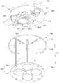
- FIG. 1is a perspective exploded view of a detecting device in accordance with a preferred embodiment of the present invention.
- FIG. 2is another perspective exploded view of the detecting device according to a preferred embodiment of the present invention.
- FIG 3is a perspective view of a detecting device in accordance with a preferred embodiment of the present invention.
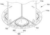
- FIG. 4is another schematic configuration diagram of a first platform in a detecting device according to a preferred embodiment of the present invention.
- FIG. 5is still another schematic configuration diagram of a first platform in a detecting apparatus according to a preferred embodiment of the present invention.
- a preferred embodiment of the present inventionprovides a detecting device for detecting an object to be tested 10.
- the detecting device of the present inventioncomprises a first platform 100, a second platform 200, a plurality of screws 310/320/330, a loading platform 400, an actuating mechanism 500 and a detecting module 600.
- the first platform 100includes a plurality of first circuit boards 110, and the plurality of first circuit boards 110 are coupled to each other. At least a portion of the first circuit board 110 is soldered to each other and electrically connected to each other.
- the conductive tape 121may be adhered as shown in FIG. 4 to connect the plurality of first circuit boards 110 to each other.
- a plurality of first circuit boards 110are connected by wires 122.
- the plurality of first circuit boards 110include a bottom plate 110a and a top plate 110b disposed in parallel with each other, and the bottom plate 110a and the top plate 110b are horizontally disposed.
- the plurality of first circuit boards 110further includes a plurality of vertical plates 110c perpendicular to the bottom plate 110a and the top plate 110b, and each of the vertical plates 110c is respectively connected to the bottom plate 110a and the top plate 110b.
- the bottom plate 110a and the top plate 110bare respectively circular plates
- the vertical plate 110cis a pair of rectangular plates
- the vertical plates 110care vertically arranged and cross-connected.
- the top plate 110bis provided with a hole electrode 111b and a groove electrode 112b electrically connected to the top plate 110b
- the top plate 110bis further provided with an electrode piece 113b electrically connected to the top plate 110b.
- the second platform 200preferably includes a second circuit board 210.
- the second circuit board 210is provided with a plurality of nuts 221, 222, and 223, and the nuts 221, 222, and 223 are respectively electrically connected.
- the second circuit board 210in the present embodiment, preferably has three nuts 221, 222, 223.
- the number of the screws 310, 320, 330preferably corresponds to the number of nuts 221, 222, 223, and each of the screws 310, 320, 330 corresponds to each of the nuts 221, 222, 223, respectively.
- 320, 330are respectively screwed to the corresponding nuts 221, 222, 223 and abut against the top plate 110b of the first platform 100, thereby being connected between the first platform 100 and the second platform 200 to connect the second platform 200 Supported on the top plate 110b of the first platform 100.
- the plurality of screws 310, 320, and 330are respectively abutted on the hole electrode 111b, the groove electrode 112b, and an electrode piece 113b, thereby being electrically connected between the first platform 100 and the second platform 200.
- the screws 310, 320, and 330are twisted, the screw 310 abutting against the hole electrode 111b is fixed, and the screw 320 abutting on the groove electrode 112b has a linear degree of freedom along the groove electrode 112b, and the screw 330 abuts against the electrode piece 113b.
- the stage 400is carried on the top plate 110b of the first platform 100 for carrying the object to be tested 10.
- the actuation mechanism 500is disposed on the first platform 100.
- the actuation mechanism 500includes a plurality of piezoelectric horns 510 disposed on the first platform 100 and the actuation mechanism 500 interlocks the stage 400.
- the piezoelectric horn 510is disposed on one surface of the bottom plate 110a and disposed toward the top plate 110b. Each piezoelectric horn 510 is electrically connected to the bottom plate 110a.
- the actuation mechanism 500also includes a plurality of jacks 520 that correspond to the plurality of piezoelectric horns 510.
- Each of the jacks 520is movably disposed through the top plate 110b. One end of each of the jacks 520 abuts the corresponding piezoelectric horn 510, and the stage 400 is carried on the other end of the plurality of jacks 520.
- the tilting angle of the stage 400can be adjusted by energizing each of the horns to push the corresponding jack 520.
- the detecting module 600is disposed on the second platform 200 for detecting the object to be tested 10 , and the detecting module 600 is preferably disposed on the second circuit board 210 and electrically connected to the second circuit board 210 .
- the detecting module 600includes a probe 610 and an optical detecting component 620.
- the probe 610is configured to face the surface of the object to be tested 10, and the optical detecting component 620 is configured to read the action of the probe 610.
- the optical detecting component 620is preferably electrically connected to the second circuit board 210.
- the optical detecting component 620can be an optical detecting component 620 capable of forming an optical lever, or can be an optical detecting component 620 like an optical disk reading head.
- the relative position of the stage 400 and the probe 610can be adjusted by adjusting the inclination of the stage 400, but the invention is not limited thereto.
- the aforementioned actuation mechanism 500can also be disposed on the second platform 200 and interlocked with the detection module 600.
- the piezoelectric horn 510 of the actuating mechanism 500can also be disposed on the second circuit board 210, and connected between the corresponding piezoelectric horn 510 and the detecting module 600 by the jack 520, thereby adjusting the check.
- the relative position of the stage 400 and the probe 610can be adjusted by measuring the inclination of the module 600.
- Each of the screws 310, 320, and 330respectively abuts and electrically connects the hole electrode 111b, the groove electrode 112b, and the electrode pad 113b on the top plate 110b of the first platform 100, thereby enabling the first platform 100 and the second platform 200 to be electrically connected.
- the connectionis made such that the detection module 600 on the second platform 200 can be electrically connected to the circuit boards 110 of the first platform 100. Therefore, corresponding circuits can be disposed on the circuit boards 110 of the first platform 100 to operate the detection module 600.
- the detecting device of the present inventionis mainly made by splicing a circuit board. Since the circuit board is easy to manufacture and low in cost, the assembly method of the splicing is also easy to assemble, so that the selling price of the detecting device can be greatly reduced and mass production is facilitated. Furthermore, the detecting device of the present invention is mainly made of a circuit board, and its weight is much smaller than that of the existing atomic force microscope, so that it is easy to carry.
Landscapes
- Physics & Mathematics (AREA)
- Health & Medical Sciences (AREA)
- General Health & Medical Sciences (AREA)
- General Physics & Mathematics (AREA)
- Nuclear Medicine, Radiotherapy & Molecular Imaging (AREA)
- Radiology & Medical Imaging (AREA)
- Geophysics And Detection Of Objects (AREA)
- Tests Of Electronic Circuits (AREA)
- Microscoopes, Condenser (AREA)
Abstract
Description
Translated fromChinese本发明有关于检测装置,尤指一种易于制造的检测装置。The invention relates to a detection device, and more particularly to a detection device that is easy to manufacture.
原子力显微镜为一种用于检测微小对象的检测装置。原子力显微镜借由一探针接触对象的表面并且沿对象表面移动,再借由光杠杆来读取探针的微小作动,因此而能够精确量测到微小对象的外形。现有的原子力显微镜其本体均由金属制成,因此不但材料成本昂贵、制造加工不易而且笨动不便于携带。An atomic force microscope is a detection device for detecting minute objects. The atomic force microscope touches the surface of the object by a probe and moves along the surface of the object, and then the light lever is used to read the micro-actuation of the probe, so that the shape of the minute object can be accurately measured. The existing atomic force microscope has its body made of metal, so that the material is expensive, the manufacturing process is not easy, and it is not easy to carry.
发明内容Summary of the invention
本发明提供一种易于制造的检测装置。The present invention provides a detection device that is easy to manufacture.
本发明提供一种检测装置,用于检测一待测物,包括:The invention provides a detecting device for detecting a test object, comprising:
一第一平台,包含相互榫接组合的多个第一电路板,至少一部分的该多个第一电路板相互电性连接,该第一平台上设置有用以承载所述待测物的一载台;a first platform comprising a plurality of first circuit boards that are coupled to each other, at least a portion of the plurality of first circuit boards being electrically connected to each other, the first platform being provided with a load for carrying the object to be tested station;
一第二平台,包含至少一第二电路板,该第二平台上设置有用以检测所述待测物的一检测模块,该检测模块电性连接至少一部分的该多个第二电路板;及a second platform includes at least one second circuit board, the second platform is provided with a detecting module for detecting the object to be tested, and the detecting module is electrically connected to at least a part of the plurality of second circuit boards;
多个螺杆,连接于该第一平台及该第二平台之间。A plurality of screws are coupled between the first platform and the second platform.
进一步地,其中该第二电路板上设有对应该多个螺杆的多个螺母,且各该螺母分别电性连接第二电路板,各该螺杆分别螺接在对应的该螺母并且抵接于第一平台。Further, the second circuit board is provided with a plurality of nuts corresponding to the plurality of screws, and each of the nuts is electrically connected to the second circuit board, and the screws are respectively screwed to the corresponding nuts and abutted on the second circuit board. The first platform.
进一步地,其中一该第一电路板上设有一孔电极、一槽电极以及一电极片,其中一该螺杆抵接该孔电极,另一该螺杆抵接该槽电极,再另一该螺杆抵接该电极片。Further, one of the first circuit boards is provided with a hole electrode, a groove electrode and an electrode piece, wherein one screw abuts the hole electrode, the other screw abuts the groove electrode, and the other screw abuts Connect the electrode sheet.
进一步地,其中该多个螺杆分别电性连连接该孔电极、该槽电极以及该电极片而使该第一平台电性连接该第二平台。Further, the plurality of screws are electrically connected to the hole electrode, the groove electrode and the electrode piece to electrically connect the first platform to the second platform.
进一步地,还包括设置在该第一平台的一致动机构。Further, an actuating mechanism disposed on the first platform is further included.
进一步地,其中该致动机构连动该载台。Further, wherein the actuating mechanism interlocks the stage.
进一步地,其中该致动机构包含设置在该第一平台的多个压电喇叭,以及连接在对应的该压电喇叭以及该致动机构之间的多个顶杆。Further, wherein the actuating mechanism comprises a plurality of piezoelectric horns disposed on the first platform, and a plurality of rams connected between the corresponding piezoelectric horns and the actuating mechanism.
进一步地,还包括设置在该第二平台的一致动机构。Further, an actuating mechanism disposed on the second platform is further included.
进一步地,其中该致动机构连动该检测模块。Further, wherein the actuating mechanism interlocks the detecting module.
进一步地,其中该致动机构包含设置在该第二平台的多个压电喇叭以及连接在对应的该压电喇叭以及该致动机构之间的多个顶杆。Further, wherein the actuating mechanism comprises a plurality of piezoelectric horns disposed on the second platform and a plurality of rams connected between the corresponding piezoelectric horn and the actuating mechanism.
进一步地,其中各该螺杆分别电性连其中一该第一电路板以及其中一该第二电路板。Further, each of the screws is electrically connected to one of the first circuit boards and one of the second circuit boards.
进一步地,其中该检测模块包含一探针。Further, wherein the detecting module comprises a probe.
进一步地,其中该检测模块包含一光学检测组件。Further, wherein the detecting module comprises an optical detecting component.
本发明具有的优点在于:The invention has the advantages of:
本发明提供的检测装置主要由电路板榫接制成,其制作容易、成本低廉、易于组装,而且体积小、轻量,进而便于携带。The detecting device provided by the invention is mainly made of a circuit board, which is easy to manufacture, low in cost, easy to assemble, small in size, light in weight, and convenient to carry.
图1为本发明较佳实施例的检测装置的一立体分解示意图。1 is a perspective exploded view of a detecting device in accordance with a preferred embodiment of the present invention.
图2为本发明较佳实施例的检测装置的另一立体分解示意图。2 is another perspective exploded view of the detecting device according to a preferred embodiment of the present invention.
图3为本发明较佳实施例的检测装置的立体示意图。3 is a perspective view of a detecting device in accordance with a preferred embodiment of the present invention.
图4为本发明较佳实施例的检测装置之中第一平台的另一可能配置示意图。4 is another schematic configuration diagram of a first platform in a detecting device according to a preferred embodiment of the present invention.
图5为本发明较佳实施例的检测装置之中第一平台的又另一可能配置示意图。FIG. 5 is still another schematic configuration diagram of a first platform in a detecting apparatus according to a preferred embodiment of the present invention.
图中:In the picture:
10 待测物;10 object to be tested;
100 第一平台;100 first platform;
110 第一电路板;110 first circuit board;
110a 底板;110a bottom plate;
110b 顶板;110b top plate;
111b 孔电极;111b hole electrode;
112b 槽电极;112b slot electrode;
113b 电极片;113b electrode sheet;
110c 立板;110c vertical board;
200 第二平台;200 second platform;
210 第二电路板;210 second circuit board;
221、222、223 螺母;221, 222, 223 nuts;
310、320、330 螺杆;310, 320, 330 screws;
400 载台;400 stages;
500 致动机构;500 actuating agencies;
510 压电喇叭;510 piezoelectric horn;
520 顶杆;520 ejector
600 检测模块;600 detection module;
610 探针;610 probe;
620 光学检测组件。620 Optical inspection assembly.
下面结合附图和具体实施例对本发明作进一步说明,以使本领域的技术人员可以更好地理解本发明并能予以实施,但所举实施例不作为对本发明的限定。The present invention will be further described in conjunction with the accompanying drawings and specific embodiments, which are to be understood by those skilled in the art.
参阅图1至图3,本发明的较佳实施例提供一种检测装置,用于检测一待测物10。本发明的检测装置包含一第一平台100、一第二平台200、多个螺杆310/320/330、一载台400、一致动机构500以及一检测模块600。Referring to FIG. 1 to FIG. 3, a preferred embodiment of the present invention provides a detecting device for detecting an object to be tested 10. The detecting device of the present invention comprises a
第一平台100包含多个第一电路板110,而且该多个第一电路板110相互榫接组合。至少一部分的第一电路板110相互焊接而电性连接,但本发明不限定于此,也可以如图4所示黏贴导电胶带121借以相互导接多个第一电路板110,也可以如图5所示借由导线122连接而导接多个第一电路板110。于本实施例中,该多个第一电路板110中包含有相互平行间隔配置的底板110a以及一顶板110b,且底板110a以及顶板110b呈水平置。该多个第一电路板110中还包含有多个立板110c,该多个立板110c垂直于底板110a以及顶板110b,而且各立板110c分别榫接底板110a以及顶板110b。较佳地,底板110a以及顶板110b分别为圆板,立板110c为一对矩形板,立板110c相互垂直配置而且交叉榫接。顶板110b上开设有电性连接顶板110b的一孔电极111b以及一槽电极112b,且顶板110b上还设有电性连接顶板110b的一电极片113b。The
于本实施例中,第二平台200较佳地包含一第二电路板210,第二电路板210上设有多个螺母221、222、223,且各螺母221、222、223分别电性连接第二电路板210,于本实施例中,螺母221、222、223较佳地为三个。In this embodiment, the
于本实施例中,螺杆310、320、330的数目较佳地与螺母221、222、223的数目相对应,各螺杆310、320、330分别对应各该螺母221、222、223,各螺杆310、320、330分别螺接在对应的螺母221、222、223并且抵接于第一平台100的顶板110b,借此连接于该第一平台100及第二平台200之间而将第二平台200支撑在第一平台100的顶板110b上。较佳地,该多个螺杆310、320、330分别抵接在孔电极111b、槽电极112b以及一电极片113b,借此而电性连接于第一平台100及第二平台200之间。当扭转各螺杆310、320、330时,抵接于孔电极111b的螺杆310固定,抵接于槽电极112b的螺杆320具有沿槽电极112b的直线自由度,抵接于电极片113b的螺杆330具有沿电极片113b的平面自由度,借此而能够通过当扭转螺杆310/320/330以调校第二平台200的水平。In the present embodiment, the number of the
载台400承载在第一平台100上的顶板110b上,其用以承载待测物10。The
于本实施例中,致动机构500设置在第一平台100。致动机构500包括设置在该第一平台100的多个压电喇叭510且致动机构500连动载台400。压电喇叭510设置在底板110a的一面上而且朝向顶板110b配置,各压电喇叭510分别电性连接底板110a。致动机构500还包括对应该多个压电喇叭510的多个顶杆520。In the present embodiment, the
各顶杆520分别可活动地贯穿顶板110b配置,各顶杆520的一端抵接对应的压电喇叭510,载台400则承载在该多个顶杆520的另一端上。借由对各喇叭通电而能够推顶对应顶杆520,借此调整载台400的倾角。Each of the
检测模块600设置在第二平台200上以用于检测待测物10,检测模块600较佳地设置在第二电路板210上并且电性连接第二电路板210。检测模块600包含有一探针610以及一光学检测组件620,探针610朝向载台400配置而能够用以接触待测物10的表面,光学检测组件620用以读取探针610的作动,光学检测组件620较佳地电性连接第二电路板210。其中,光学检测组件620可以是能够形成光杠杆的光学检测组件620,也可以是一如同光盘读取头的光学检测组件620。The detecting
借由调整载台400的倾角而能够调整载台400与探针610的相对位置,但本发明不以此为限。例如,前述的致动机构500也可以设置在第二平台200上且连动检测模块600。致动机构500的压电喇叭510也可以设置在第二电路板210,并且借由顶杆520连接在对应的压电喇叭510及检测模块600之间,借此调整检测模块600的倾角而能够调整载台400与探针610的相对位置。The relative position of the
各螺杆310、320、330分别抵接而电性连接第一平台100顶板110b上的孔电极111b、槽电极112b以及一电极片113b,借此能够将第一平台100与第二平台200电性连接,使得第二平台200上的检测模块600能够电性连接第一平台100的各电路板110,因此能够在第一平台100的各电路板110上布设对应的电路来操作检测模块600。Each of the
综上所述,本发明的检测装置主要由电路板榫接制成。由于电路板制作容易且成本低廉,榫接的组装方式也易于组装,因此能够大幅降低检测装置的售价并且有利于量产。再者,本发明的检测装置主要由电路板制成,其重量远小于现有的原子力显微镜,因此便于携带。In summary, the detecting device of the present invention is mainly made by splicing a circuit board. Since the circuit board is easy to manufacture and low in cost, the assembly method of the splicing is also easy to assemble, so that the selling price of the detecting device can be greatly reduced and mass production is facilitated. Furthermore, the detecting device of the present invention is mainly made of a circuit board, and its weight is much smaller than that of the existing atomic force microscope, so that it is easy to carry.
以上所述实施例仅是为充分说明本发明而所举的较佳的实施例,本发明的保护范围不限于此。本技术领域的技术人员在本发明基础上所作的等同替代或变换,均在本发明的保护范围之内。本发明的保护范围以权利要求书为准。The embodiments described above are merely preferred embodiments for the purpose of fully illustrating the invention, and the scope of the invention is not limited thereto. Equivalent substitutions or modifications made by those skilled in the art based on the present invention are within the scope of the present invention. The scope of the invention is defined by the claims.
Claims (13)
Translated fromChinesePriority Applications (2)
| Application Number | Priority Date | Filing Date | Title |
|---|---|---|---|
| CN201580052468.8ACN106796247A (en) | 2015-01-07 | 2015-12-29 | Detection device |
| US15/532,502US10338097B2 (en) | 2015-01-07 | 2015-12-29 | Joggle jointed detection apparatus |
Applications Claiming Priority (2)
| Application Number | Priority Date | Filing Date | Title |
|---|---|---|---|
| US201562100850P | 2015-01-07 | 2015-01-07 | |
| US62/100,850 | 2015-01-07 |
Publications (1)
| Publication Number | Publication Date |
|---|---|
| WO2016110198A1true WO2016110198A1 (en) | 2016-07-14 |
Family
ID=56355505
Family Applications (1)
| Application Number | Title | Priority Date | Filing Date |
|---|---|---|---|
| PCT/CN2015/099360CeasedWO2016110198A1 (en) | 2015-01-07 | 2015-12-29 | Detection apparatus |
Country Status (3)
| Country | Link |
|---|---|
| US (1) | US10338097B2 (en) |
| CN (1) | CN106796247A (en) |
| WO (1) | WO2016110198A1 (en) |
Families Citing this family (1)
| Publication number | Priority date | Publication date | Assignee | Title |
|---|---|---|---|---|
| CN111413611B (en)* | 2020-05-19 | 2024-05-17 | 华侨大学 | Circuit board node performance detection platform |
Citations (7)
| Publication number | Priority date | Publication date | Assignee | Title |
|---|---|---|---|---|
| CN1150253A (en)* | 1994-11-28 | 1997-05-21 | 松下电器产业株式会社 | atomic force microscope |
| CN201590798U (en)* | 2009-12-21 | 2010-09-22 | 马夸特开关(上海)有限公司 | Large-current speed regulating switch |
| WO2012115653A1 (en)* | 2011-02-25 | 2012-08-30 | Agilent Technologies, Inc. | Atomic force microscopy controller and method |
| US20130340126A1 (en)* | 2006-04-25 | 2013-12-19 | Asylum Research Corporation | Multiple Frequency Atomic Force Microscopy |
| CN103808967A (en)* | 2014-02-23 | 2014-05-21 | 北京航空航天大学 | Imaging system of atomic force microscope on the basis of quartz tuning fork probe |
| CN103941044A (en)* | 2014-04-06 | 2014-07-23 | 南开大学 | Cross-scale high-precision sample feeding mechanism of atomic force microscope |
| CN104062466A (en)* | 2014-07-01 | 2014-09-24 | 哈尔滨工业大学 | Micro-nano structure sidewall surface imaging device based on atomic force microscope (AFM) and imaging method thereof |
Family Cites Families (4)
| Publication number | Priority date | Publication date | Assignee | Title |
|---|---|---|---|---|
| US6335864B1 (en)* | 1999-01-20 | 2002-01-01 | Mannesmann Vdo Ag | Indicator module |
| TW538096B (en)* | 1999-06-25 | 2003-06-21 | Shinetsu Chemical Co | Nitrogen atom-containing polysiloxanes, their preparation, and fiber and fabric finishing agent compositions |
| JP6221358B2 (en)* | 2013-06-04 | 2017-11-01 | 日本電産リード株式会社 | Substrate inspection method and substrate inspection apparatus |
| CN105158609B (en)* | 2015-09-11 | 2018-12-28 | 京东方科技集团股份有限公司 | The method of lighting module detecting device, test point lamp module and display panel |
- 2015
- 2015-12-29WOPCT/CN2015/099360patent/WO2016110198A1/ennot_activeCeased
- 2015-12-29CNCN201580052468.8Apatent/CN106796247A/enactivePending
- 2015-12-29USUS15/532,502patent/US10338097B2/ennot_activeExpired - Fee Related
Patent Citations (7)
| Publication number | Priority date | Publication date | Assignee | Title |
|---|---|---|---|---|
| CN1150253A (en)* | 1994-11-28 | 1997-05-21 | 松下电器产业株式会社 | atomic force microscope |
| US20130340126A1 (en)* | 2006-04-25 | 2013-12-19 | Asylum Research Corporation | Multiple Frequency Atomic Force Microscopy |
| CN201590798U (en)* | 2009-12-21 | 2010-09-22 | 马夸特开关(上海)有限公司 | Large-current speed regulating switch |
| WO2012115653A1 (en)* | 2011-02-25 | 2012-08-30 | Agilent Technologies, Inc. | Atomic force microscopy controller and method |
| CN103808967A (en)* | 2014-02-23 | 2014-05-21 | 北京航空航天大学 | Imaging system of atomic force microscope on the basis of quartz tuning fork probe |
| CN103941044A (en)* | 2014-04-06 | 2014-07-23 | 南开大学 | Cross-scale high-precision sample feeding mechanism of atomic force microscope |
| CN104062466A (en)* | 2014-07-01 | 2014-09-24 | 哈尔滨工业大学 | Micro-nano structure sidewall surface imaging device based on atomic force microscope (AFM) and imaging method thereof |
Also Published As
| Publication number | Publication date |
|---|---|
| CN106796247A (en) | 2017-05-31 |
| US20170370963A1 (en) | 2017-12-28 |
| US10338097B2 (en) | 2019-07-02 |
Similar Documents
| Publication | Publication Date | Title |
|---|---|---|
| US7428783B2 (en) | Testing system for flatness and parallelism | |
| US20080210015A1 (en) | Failure analysis system and method using the same | |
| JP7148212B2 (en) | Inspection jig and board inspection device | |
| TW201937648A (en) | Wafer prober | |
| KR100826257B1 (en) | FPC inspection device for portable electronic devices | |
| CN104508498B (en) | Probe unit, substrate inspection device, and probe unit manufacturing method | |
| TW201317543A (en) | Planeness testing device | |
| JP2008309787A (en) | Probe assembly for probe card | |
| CN215986161U (en) | Test fixture and test device | |
| JP2017187456A (en) | Probe card | |
| JP5970218B2 (en) | Probe device | |
| KR101120405B1 (en) | Probe block assembly | |
| WO2016110198A1 (en) | Detection apparatus | |
| JP2017036997A (en) | Inspection apparatus and inspection method for double-sided circuit board | |
| JP4684805B2 (en) | Probe device and method for adjusting contact pressure between object to be inspected and probe | |
| CN206362329U (en) | Part deformation detecting device | |
| CN101846709A (en) | Flexible circuit board line short circuit test board and test method | |
| CN103575439B (en) | For the device of bonding wire tensile test | |
| TWI727373B (en) | Test fixture and test machine | |
| JP3154264U (en) | Probe unit for probe pin and board inspection | |
| TWM469489U (en) | Testing assembly and electrical testing device | |
| KR101257226B1 (en) | Apparatus of film type test probe | |
| JP2010210478A (en) | Probe card | |
| JP4406218B2 (en) | Inspection device provided with probe, and positioning method by positioning mechanism of inspection device provided with probe | |
| CN219590346U (en) | Atomic force microscope probe seat |
Legal Events
| Date | Code | Title | Description |
|---|---|---|---|
| 121 | Ep: the epo has been informed by wipo that ep was designated in this application | Ref document number:15876698 Country of ref document:EP Kind code of ref document:A1 | |
| WWE | Wipo information: entry into national phase | Ref document number:15532502 Country of ref document:US | |
| NENP | Non-entry into the national phase | Ref country code:DE | |
| 122 | Ep: pct application non-entry in european phase | Ref document number:15876698 Country of ref document:EP Kind code of ref document:A1 |