WO2016084700A1 - Semiconductor device and method for manufacturing same - Google Patents
Semiconductor device and method for manufacturing sameDownload PDFInfo
- Publication number
- WO2016084700A1 WO2016084700A1PCT/JP2015/082539JP2015082539WWO2016084700A1WO 2016084700 A1WO2016084700 A1WO 2016084700A1JP 2015082539 WJP2015082539 WJP 2015082539WWO 2016084700 A1WO2016084700 A1WO 2016084700A1
- Authority
- WO
- WIPO (PCT)
- Prior art keywords
- layer
- oxide film
- insulating layer
- drain electrode
- source
- Prior art date
Links
- 239000004065semiconductorSubstances0.000titleclaimsabstractdescription367
- 238000000034methodMethods0.000titleclaimsdescription70
- 238000004519manufacturing processMethods0.000titleclaimsdescription35
- 239000010410layerSubstances0.000claimsabstractdescription906
- 239000010408filmSubstances0.000claimsabstractdescription438
- 239000010949copperSubstances0.000claimsabstractdescription236
- 239000011229interlayerSubstances0.000claimsabstractdescription129
- QPLDLSVMHZLSFG-UHFFFAOYSA-NCopper oxideChemical compound[Cu]=OQPLDLSVMHZLSFG-UHFFFAOYSA-N0.000claimsabstractdescription44
- 229910052802copperInorganic materials0.000claimsabstractdescription40
- RYGMFSIKBFXOCR-UHFFFAOYSA-NCopperChemical compound[Cu]RYGMFSIKBFXOCR-UHFFFAOYSA-N0.000claimsabstractdescription39
- 239000005751Copper oxideSubstances0.000claimsabstractdescription37
- 229910000431copper oxideInorganic materials0.000claimsabstractdescription37
- 239000010409thin filmSubstances0.000claimsabstractdescription24
- 239000000758substrateSubstances0.000claimsdescription94
- 230000003647oxidationEffects0.000claimsdescription69
- 238000007254oxidation reactionMethods0.000claimsdescription69
- 238000004140cleaningMethods0.000claimsdescription47
- 239000013522chelantSubstances0.000claimsdescription42
- 239000010936titaniumSubstances0.000claimsdescription33
- 229910007541Zn OInorganic materials0.000claimsdescription24
- QVGXLLKOCUKJST-UHFFFAOYSA-Natomic oxygenChemical compound[O]QVGXLLKOCUKJST-UHFFFAOYSA-N0.000claimsdescription17
- 239000001301oxygenSubstances0.000claimsdescription17
- 229910052760oxygenInorganic materials0.000claimsdescription17
- 229910052750molybdenumInorganic materials0.000claimsdescription12
- 229910052719titaniumInorganic materials0.000claimsdescription12
- 230000001590oxidative effectEffects0.000claimsdescription11
- ZOKXTWBITQBERF-UHFFFAOYSA-NMolybdenumChemical compound[Mo]ZOKXTWBITQBERF-UHFFFAOYSA-N0.000claimsdescription6
- RTAQQCXQSZGOHL-UHFFFAOYSA-NTitaniumChemical compound[Ti]RTAQQCXQSZGOHL-UHFFFAOYSA-N0.000claimsdescription6
- 239000011733molybdenumSubstances0.000claimsdescription6
- 238000009413insulationMethods0.000claimsdescription2
- 229910000881Cu alloyInorganic materials0.000description156
- 229910052751metalInorganic materials0.000description55
- 239000002184metalSubstances0.000description51
- 229910044991metal oxideInorganic materials0.000description30
- 150000004706metal oxidesChemical class0.000description30
- 239000000243solutionSubstances0.000description19
- 238000009832plasma treatmentMethods0.000description16
- 239000011159matrix materialSubstances0.000description14
- 238000004544sputter depositionMethods0.000description14
- 230000015572biosynthetic processEffects0.000description13
- 239000000463materialSubstances0.000description13
- 230000001681protective effectEffects0.000description13
- 239000000654additiveSubstances0.000description12
- 230000000996additive effectEffects0.000description12
- 230000000052comparative effectEffects0.000description11
- 229910052581Si3N4Inorganic materials0.000description10
- 229910045601alloyInorganic materials0.000description10
- 239000000956alloySubstances0.000description10
- 238000005530etchingMethods0.000description10
- HQVNEWCFYHHQES-UHFFFAOYSA-Nsilicon nitrideChemical compoundN12[Si]34N5[Si]62N3[Si]51N64HQVNEWCFYHHQES-UHFFFAOYSA-N0.000description10
- 239000011701zincSubstances0.000description10
- 238000000059patterningMethods0.000description9
- XLOMVQKBTHCTTD-UHFFFAOYSA-Nzinc oxideInorganic materials[Zn]=OXLOMVQKBTHCTTD-UHFFFAOYSA-N0.000description9
- 229910004298SiO 2Inorganic materials0.000description8
- 239000007789gasSubstances0.000description8
- 238000002845discolorationMethods0.000description7
- 229910004205SiNXInorganic materials0.000description6
- XUIMIQQOPSSXEZ-UHFFFAOYSA-NSiliconChemical compound[Si]XUIMIQQOPSSXEZ-UHFFFAOYSA-N0.000description6
- 239000003990capacitorSubstances0.000description6
- 230000000694effectsEffects0.000description6
- 230000006870functionEffects0.000description6
- 229910052710siliconInorganic materials0.000description6
- 239000010703siliconSubstances0.000description6
- VYPSYNLAJGMNEJ-UHFFFAOYSA-NSilicium dioxideChemical compoundO=[Si]=OVYPSYNLAJGMNEJ-UHFFFAOYSA-N0.000description5
- 238000005401electroluminescenceMethods0.000description5
- 239000012535impuritySubstances0.000description5
- 229910052738indiumInorganic materials0.000description5
- 239000000203mixtureSubstances0.000description5
- 229910052814silicon oxideInorganic materials0.000description5
- 229910052725zincInorganic materials0.000description5
- 239000011787zinc oxideSubstances0.000description5
- 229910004286SiNxOyInorganic materials0.000description4
- 229910020286SiOxNyInorganic materials0.000description4
- 229910052782aluminiumInorganic materials0.000description4
- 238000005229chemical vapour depositionMethods0.000description4
- 229910052733galliumInorganic materials0.000description4
- 239000004973liquid crystal related substanceSubstances0.000description4
- 238000012545processingMethods0.000description4
- WGTYBPLFGIVFAS-UHFFFAOYSA-Mtetramethylammonium hydroxideChemical compound[OH-].C[N+](C)(C)CWGTYBPLFGIVFAS-UHFFFAOYSA-M0.000description4
- 238000010586diagramMethods0.000description3
- 230000005684electric fieldEffects0.000description3
- 230000002093peripheral effectEffects0.000description3
- 239000011347resinSubstances0.000description3
- 229920005989resinPolymers0.000description3
- 229910018072Al 2 O 3Inorganic materials0.000description2
- XKRFYHLGVUSROY-UHFFFAOYSA-NArgonChemical compound[Ar]XKRFYHLGVUSROY-UHFFFAOYSA-N0.000description2
- UFHFLCQGNIYNRP-UHFFFAOYSA-NHydrogenChemical compound[H][H]UFHFLCQGNIYNRP-UHFFFAOYSA-N0.000description2
- NRTOMJZYCJJWKI-UHFFFAOYSA-NTitanium nitrideChemical compound[Ti]#NNRTOMJZYCJJWKI-UHFFFAOYSA-N0.000description2
- HCHKCACWOHOZIP-UHFFFAOYSA-NZincChemical compound[Zn]HCHKCACWOHOZIP-UHFFFAOYSA-N0.000description2
- 238000010521absorption reactionMethods0.000description2
- 229910021417amorphous siliconInorganic materials0.000description2
- GPBUGPUPKAGMDK-UHFFFAOYSA-NazanylidynemolybdenumChemical compound[Mo]#NGPBUGPUPKAGMDK-UHFFFAOYSA-N0.000description2
- CXKCTMHTOKXKQT-UHFFFAOYSA-Ncadmium oxideInorganic materials[Cd]=OCXKCTMHTOKXKQT-UHFFFAOYSA-N0.000description2
- CFEAAQFZALKQPA-UHFFFAOYSA-Ncadmium(2+);oxygen(2-)Chemical compound[O-2].[Cd+2]CFEAAQFZALKQPA-UHFFFAOYSA-N0.000description2
- 229910052791calciumInorganic materials0.000description2
- 239000011651chromiumSubstances0.000description2
- 230000007797corrosionEffects0.000description2
- 238000005260corrosionMethods0.000description2
- 239000013078crystalSubstances0.000description2
- 230000007547defectEffects0.000description2
- 230000006866deteriorationEffects0.000description2
- 239000011521glassSubstances0.000description2
- 239000001257hydrogenSubstances0.000description2
- 229910052739hydrogenInorganic materials0.000description2
- APFVFJFRJDLVQX-UHFFFAOYSA-Nindium atomChemical compound[In]APFVFJFRJDLVQX-UHFFFAOYSA-N0.000description2
- AMGQUBHHOARCQH-UHFFFAOYSA-Nindium;oxotinChemical compound[In].[Sn]=OAMGQUBHHOARCQH-UHFFFAOYSA-N0.000description2
- 230000001788irregularEffects0.000description2
- 229910052749magnesiumInorganic materials0.000description2
- 229910052748manganeseInorganic materials0.000description2
- 238000005259measurementMethods0.000description2
- 238000000206photolithographyMethods0.000description2
- 238000001878scanning electron micrographMethods0.000description2
- 238000000926separation methodMethods0.000description2
- 239000000126substanceSubstances0.000description2
- VYZAMTAEIAYCRO-UHFFFAOYSA-NChromiumChemical compound[Cr]VYZAMTAEIAYCRO-UHFFFAOYSA-N0.000description1
- 229910017518Cu ZnInorganic materials0.000description1
- 229910017752Cu-ZnInorganic materials0.000description1
- 229910017943Cu—ZnInorganic materials0.000description1
- GYHNNYVSQQEPJS-UHFFFAOYSA-NGalliumChemical compound[Ga]GYHNNYVSQQEPJS-UHFFFAOYSA-N0.000description1
- MHAJPDPJQMAIIY-UHFFFAOYSA-NHydrogen peroxideChemical compoundOOMHAJPDPJQMAIIY-UHFFFAOYSA-N0.000description1
- CBENFWSGALASAD-UHFFFAOYSA-NOzoneChemical compound[O-][O+]=OCBENFWSGALASAD-UHFFFAOYSA-N0.000description1
- 229910020923Sn-OInorganic materials0.000description1
- 229910006404SnO 2Inorganic materials0.000description1
- ATJFFYVFTNAWJD-UHFFFAOYSA-NTinChemical compound[Sn]ATJFFYVFTNAWJD-UHFFFAOYSA-N0.000description1
- 229910003077Ti−OInorganic materials0.000description1
- XAGFODPZIPBFFR-UHFFFAOYSA-NaluminiumChemical compound[Al]XAGFODPZIPBFFR-UHFFFAOYSA-N0.000description1
- 150000001412aminesChemical class0.000description1
- 238000004458analytical methodMethods0.000description1
- 238000000137annealingMethods0.000description1
- 229910052786argonInorganic materials0.000description1
- 238000004380ashingMethods0.000description1
- 229910052804chromiumInorganic materials0.000description1
- TVZPLCNGKSPOJA-UHFFFAOYSA-Ncopper zincChemical compound[Cu].[Zn]TVZPLCNGKSPOJA-UHFFFAOYSA-N0.000description1
- 238000000151depositionMethods0.000description1
- 230000008021depositionEffects0.000description1
- 238000009792diffusion processMethods0.000description1
- 239000007772electrode materialSubstances0.000description1
- 238000010438heat treatmentMethods0.000description1
- 238000003384imaging methodMethods0.000description1
- 229910010272inorganic materialInorganic materials0.000description1
- 239000011147inorganic materialSubstances0.000description1
- 238000011835investigationMethods0.000description1
- 230000001678irradiating effectEffects0.000description1
- 239000007788liquidSubstances0.000description1
- 230000015654memoryEffects0.000description1
- 239000011259mixed solutionSubstances0.000description1
- 238000012986modificationMethods0.000description1
- 230000004048modificationEffects0.000description1
- 150000004767nitridesChemical class0.000description1
- 238000002161passivationMethods0.000description1
- 238000005268plasma chemical vapour depositionMethods0.000description1
- 239000002356single layerSubstances0.000description1
- -1structureSubstances0.000description1
- 229910052715tantalumInorganic materials0.000description1
- GUVRBAGPIYLISA-UHFFFAOYSA-Ntantalum atomChemical compound[Ta]GUVRBAGPIYLISA-UHFFFAOYSA-N0.000description1
- WFKWXMTUELFFGS-UHFFFAOYSA-NtungstenChemical compound[W]WFKWXMTUELFFGS-UHFFFAOYSA-N0.000description1
- 229910052721tungstenInorganic materials0.000description1
- 239000010937tungstenSubstances0.000description1
- XLYOFNOQVPJJNP-UHFFFAOYSA-NwaterSubstancesOXLYOFNOQVPJJNP-UHFFFAOYSA-N0.000description1
- 238000001039wet etchingMethods0.000description1
Images


Classifications
- G—PHYSICS
- G02—OPTICS
- G02F—OPTICAL DEVICES OR ARRANGEMENTS FOR THE CONTROL OF LIGHT BY MODIFICATION OF THE OPTICAL PROPERTIES OF THE MEDIA OF THE ELEMENTS INVOLVED THEREIN; NON-LINEAR OPTICS; FREQUENCY-CHANGING OF LIGHT; OPTICAL LOGIC ELEMENTS; OPTICAL ANALOGUE/DIGITAL CONVERTERS
- G02F1/00—Devices or arrangements for the control of the intensity, colour, phase, polarisation or direction of light arriving from an independent light source, e.g. switching, gating or modulating; Non-linear optics
- G02F1/01—Devices or arrangements for the control of the intensity, colour, phase, polarisation or direction of light arriving from an independent light source, e.g. switching, gating or modulating; Non-linear optics for the control of the intensity, phase, polarisation or colour
- G02F1/13—Devices or arrangements for the control of the intensity, colour, phase, polarisation or direction of light arriving from an independent light source, e.g. switching, gating or modulating; Non-linear optics for the control of the intensity, phase, polarisation or colour based on liquid crystals, e.g. single liquid crystal display cells
- G02F1/133—Constructional arrangements; Operation of liquid crystal cells; Circuit arrangements
- G02F1/1333—Constructional arrangements; Manufacturing methods
- G02F1/1343—Electrodes
- H—ELECTRICITY
- H01—ELECTRIC ELEMENTS
- H01L—SEMICONDUCTOR DEVICES NOT COVERED BY CLASS H10
- H01L21/00—Processes or apparatus adapted for the manufacture or treatment of semiconductor or solid state devices or of parts thereof
- H01L21/02—Manufacture or treatment of semiconductor devices or of parts thereof
- H01L21/04—Manufacture or treatment of semiconductor devices or of parts thereof the devices having potential barriers, e.g. a PN junction, depletion layer or carrier concentration layer
- H01L21/18—Manufacture or treatment of semiconductor devices or of parts thereof the devices having potential barriers, e.g. a PN junction, depletion layer or carrier concentration layer the devices having semiconductor bodies comprising elements of Group IV of the Periodic Table or AIIIBV compounds with or without impurities, e.g. doping materials
- H01L21/28—Manufacture of electrodes on semiconductor bodies using processes or apparatus not provided for in groups H01L21/20 - H01L21/268
- H01L21/283—Deposition of conductive or insulating materials for electrodes conducting electric current
- H—ELECTRICITY
- H01—ELECTRIC ELEMENTS
- H01L—SEMICONDUCTOR DEVICES NOT COVERED BY CLASS H10
- H01L21/00—Processes or apparatus adapted for the manufacture or treatment of semiconductor or solid state devices or of parts thereof
- H01L21/02—Manufacture or treatment of semiconductor devices or of parts thereof
- H01L21/04—Manufacture or treatment of semiconductor devices or of parts thereof the devices having potential barriers, e.g. a PN junction, depletion layer or carrier concentration layer
- H01L21/18—Manufacture or treatment of semiconductor devices or of parts thereof the devices having potential barriers, e.g. a PN junction, depletion layer or carrier concentration layer the devices having semiconductor bodies comprising elements of Group IV of the Periodic Table or AIIIBV compounds with or without impurities, e.g. doping materials
- H01L21/30—Treatment of semiconductor bodies using processes or apparatus not provided for in groups H01L21/20 - H01L21/26
- H01L21/302—Treatment of semiconductor bodies using processes or apparatus not provided for in groups H01L21/20 - H01L21/26 to change their surface-physical characteristics or shape, e.g. etching, polishing, cutting
- H01L21/306—Chemical or electrical treatment, e.g. electrolytic etching
- H—ELECTRICITY
- H01—ELECTRIC ELEMENTS
- H01L—SEMICONDUCTOR DEVICES NOT COVERED BY CLASS H10
- H01L21/00—Processes or apparatus adapted for the manufacture or treatment of semiconductor or solid state devices or of parts thereof
- H01L21/70—Manufacture or treatment of devices consisting of a plurality of solid state components formed in or on a common substrate or of parts thereof; Manufacture of integrated circuit devices or of parts thereof
- H01L21/71—Manufacture of specific parts of devices defined in group H01L21/70
- H01L21/768—Applying interconnections to be used for carrying current between separate components within a device comprising conductors and dielectrics
- H—ELECTRICITY
- H01—ELECTRIC ELEMENTS
- H01L—SEMICONDUCTOR DEVICES NOT COVERED BY CLASS H10
- H01L23/00—Details of semiconductor or other solid state devices
- H01L23/52—Arrangements for conducting electric current within the device in operation from one component to another, i.e. interconnections, e.g. wires, lead frames
- H01L23/522—Arrangements for conducting electric current within the device in operation from one component to another, i.e. interconnections, e.g. wires, lead frames including external interconnections consisting of a multilayer structure of conductive and insulating layers inseparably formed on the semiconductor body
- H01L23/532—Arrangements for conducting electric current within the device in operation from one component to another, i.e. interconnections, e.g. wires, lead frames including external interconnections consisting of a multilayer structure of conductive and insulating layers inseparably formed on the semiconductor body characterised by the materials
- H01L23/53204—Conductive materials
- H01L23/53209—Conductive materials based on metals, e.g. alloys, metal silicides
- H01L23/53228—Conductive materials based on metals, e.g. alloys, metal silicides the principal metal being copper
- H—ELECTRICITY
- H01—ELECTRIC ELEMENTS
- H01L—SEMICONDUCTOR DEVICES NOT COVERED BY CLASS H10
- H01L23/00—Details of semiconductor or other solid state devices
- H01L23/52—Arrangements for conducting electric current within the device in operation from one component to another, i.e. interconnections, e.g. wires, lead frames
- H01L23/522—Arrangements for conducting electric current within the device in operation from one component to another, i.e. interconnections, e.g. wires, lead frames including external interconnections consisting of a multilayer structure of conductive and insulating layers inseparably formed on the semiconductor body
- H01L23/532—Arrangements for conducting electric current within the device in operation from one component to another, i.e. interconnections, e.g. wires, lead frames including external interconnections consisting of a multilayer structure of conductive and insulating layers inseparably formed on the semiconductor body characterised by the materials
- H01L23/53204—Conductive materials
- H01L23/53209—Conductive materials based on metals, e.g. alloys, metal silicides
- H01L23/53257—Conductive materials based on metals, e.g. alloys, metal silicides the principal metal being a refractory metal
- H—ELECTRICITY
- H01—ELECTRIC ELEMENTS
- H01L—SEMICONDUCTOR DEVICES NOT COVERED BY CLASS H10
- H01L23/00—Details of semiconductor or other solid state devices
- H01L23/544—Marks applied to semiconductor devices or parts, e.g. registration marks, alignment structures, wafer maps
- H—ELECTRICITY
- H10—SEMICONDUCTOR DEVICES; ELECTRIC SOLID-STATE DEVICES NOT OTHERWISE PROVIDED FOR
- H10D—INORGANIC ELECTRIC SEMICONDUCTOR DEVICES
- H10D30/00—Field-effect transistors [FET]
- H10D30/60—Insulated-gate field-effect transistors [IGFET]
- H10D30/67—Thin-film transistors [TFT]
- H10D30/6729—Thin-film transistors [TFT] characterised by the electrodes
- H—ELECTRICITY
- H10—SEMICONDUCTOR DEVICES; ELECTRIC SOLID-STATE DEVICES NOT OTHERWISE PROVIDED FOR
- H10D—INORGANIC ELECTRIC SEMICONDUCTOR DEVICES
- H10D30/00—Field-effect transistors [FET]
- H10D30/60—Insulated-gate field-effect transistors [IGFET]
- H10D30/67—Thin-film transistors [TFT]
- H10D30/674—Thin-film transistors [TFT] characterised by the active materials
- H10D30/6755—Oxide semiconductors, e.g. zinc oxide, copper aluminium oxide or cadmium stannate
- H10D30/6756—Amorphous oxide semiconductors
- H—ELECTRICITY
- H10—SEMICONDUCTOR DEVICES; ELECTRIC SOLID-STATE DEVICES NOT OTHERWISE PROVIDED FOR
- H10D—INORGANIC ELECTRIC SEMICONDUCTOR DEVICES
- H10D86/00—Integrated devices formed in or on insulating or conducting substrates, e.g. formed in silicon-on-insulator [SOI] substrates or on stainless steel or glass substrates
- H10D86/40—Integrated devices formed in or on insulating or conducting substrates, e.g. formed in silicon-on-insulator [SOI] substrates or on stainless steel or glass substrates characterised by multiple TFTs
- H10D86/421—Integrated devices formed in or on insulating or conducting substrates, e.g. formed in silicon-on-insulator [SOI] substrates or on stainless steel or glass substrates characterised by multiple TFTs having a particular composition, shape or crystalline structure of the active layer
- H10D86/423—Integrated devices formed in or on insulating or conducting substrates, e.g. formed in silicon-on-insulator [SOI] substrates or on stainless steel or glass substrates characterised by multiple TFTs having a particular composition, shape or crystalline structure of the active layer comprising semiconductor materials not belonging to the Group IV, e.g. InGaZnO
- H—ELECTRICITY
- H10—SEMICONDUCTOR DEVICES; ELECTRIC SOLID-STATE DEVICES NOT OTHERWISE PROVIDED FOR
- H10D—INORGANIC ELECTRIC SEMICONDUCTOR DEVICES
- H10D86/00—Integrated devices formed in or on insulating or conducting substrates, e.g. formed in silicon-on-insulator [SOI] substrates or on stainless steel or glass substrates
- H10D86/40—Integrated devices formed in or on insulating or conducting substrates, e.g. formed in silicon-on-insulator [SOI] substrates or on stainless steel or glass substrates characterised by multiple TFTs
- H10D86/441—Interconnections, e.g. scanning lines
- H—ELECTRICITY
- H10—SEMICONDUCTOR DEVICES; ELECTRIC SOLID-STATE DEVICES NOT OTHERWISE PROVIDED FOR
- H10D—INORGANIC ELECTRIC SEMICONDUCTOR DEVICES
- H10D86/00—Integrated devices formed in or on insulating or conducting substrates, e.g. formed in silicon-on-insulator [SOI] substrates or on stainless steel or glass substrates
- H10D86/40—Integrated devices formed in or on insulating or conducting substrates, e.g. formed in silicon-on-insulator [SOI] substrates or on stainless steel or glass substrates characterised by multiple TFTs
- H10D86/451—Integrated devices formed in or on insulating or conducting substrates, e.g. formed in silicon-on-insulator [SOI] substrates or on stainless steel or glass substrates characterised by multiple TFTs characterised by the compositions or shapes of the interlayer dielectrics
- H—ELECTRICITY
- H10—SEMICONDUCTOR DEVICES; ELECTRIC SOLID-STATE DEVICES NOT OTHERWISE PROVIDED FOR
- H10D—INORGANIC ELECTRIC SEMICONDUCTOR DEVICES
- H10D86/00—Integrated devices formed in or on insulating or conducting substrates, e.g. formed in silicon-on-insulator [SOI] substrates or on stainless steel or glass substrates
- H10D86/40—Integrated devices formed in or on insulating or conducting substrates, e.g. formed in silicon-on-insulator [SOI] substrates or on stainless steel or glass substrates characterised by multiple TFTs
- H10D86/60—Integrated devices formed in or on insulating or conducting substrates, e.g. formed in silicon-on-insulator [SOI] substrates or on stainless steel or glass substrates characterised by multiple TFTs wherein the TFTs are in active matrices
- H—ELECTRICITY
- H10—SEMICONDUCTOR DEVICES; ELECTRIC SOLID-STATE DEVICES NOT OTHERWISE PROVIDED FOR
- H10D—INORGANIC ELECTRIC SEMICONDUCTOR DEVICES
- H10D99/00—Subject matter not provided for in other groups of this subclass
- G—PHYSICS
- G02—OPTICS
- G02F—OPTICAL DEVICES OR ARRANGEMENTS FOR THE CONTROL OF LIGHT BY MODIFICATION OF THE OPTICAL PROPERTIES OF THE MEDIA OF THE ELEMENTS INVOLVED THEREIN; NON-LINEAR OPTICS; FREQUENCY-CHANGING OF LIGHT; OPTICAL LOGIC ELEMENTS; OPTICAL ANALOGUE/DIGITAL CONVERTERS
- G02F1/00—Devices or arrangements for the control of the intensity, colour, phase, polarisation or direction of light arriving from an independent light source, e.g. switching, gating or modulating; Non-linear optics
- G02F1/01—Devices or arrangements for the control of the intensity, colour, phase, polarisation or direction of light arriving from an independent light source, e.g. switching, gating or modulating; Non-linear optics for the control of the intensity, phase, polarisation or colour
- G02F1/13—Devices or arrangements for the control of the intensity, colour, phase, polarisation or direction of light arriving from an independent light source, e.g. switching, gating or modulating; Non-linear optics for the control of the intensity, phase, polarisation or colour based on liquid crystals, e.g. single liquid crystal display cells
- G02F1/133—Constructional arrangements; Operation of liquid crystal cells; Circuit arrangements
- G02F1/136—Liquid crystal cells structurally associated with a semi-conducting layer or substrate, e.g. cells forming part of an integrated circuit
- G02F1/1362—Active matrix addressed cells
- G02F1/1368—Active matrix addressed cells in which the switching element is a three-electrode device
- H—ELECTRICITY
- H01—ELECTRIC ELEMENTS
- H01L—SEMICONDUCTOR DEVICES NOT COVERED BY CLASS H10
- H01L2223/00—Details relating to semiconductor or other solid state devices covered by the group H01L23/00
- H01L2223/544—Marks applied to semiconductor devices or parts
- H01L2223/54426—Marks applied to semiconductor devices or parts for alignment
- H—ELECTRICITY
- H01—ELECTRIC ELEMENTS
- H01L—SEMICONDUCTOR DEVICES NOT COVERED BY CLASS H10
- H01L2924/00—Indexing scheme for arrangements or methods for connecting or disconnecting semiconductor or solid-state bodies as covered by H01L24/00
- H01L2924/0001—Technical content checked by a classifier
- H01L2924/0002—Not covered by any one of groups H01L24/00, H01L24/00 and H01L2224/00
Definitions
- the present inventionrelates to a semiconductor device formed using an oxide semiconductor and a manufacturing method thereof.
- An active matrix substrate used for a liquid crystal display device or the likeincludes a switching element such as a thin film transistor (hereinafter, “TFT”) for each pixel.
- TFTthin film transistor
- oxide semiconductor TFToxide semiconductor TFT
- a protective film(passivation layer) is formed on the oxide semiconductor layer by, for example, a CVD method or a sputtering method using plasma in order to suppress deterioration of TFT characteristics with time.
- the protective filmis formed, the surface of the oxide semiconductor layer may be damaged. Specifically, oxygen vacancies may be generated in the oxide semiconductor layer, or hydrogen may diffuse from the protective film, so that the surface of the oxide semiconductor layer may have low resistance (conductivity).
- the threshold voltageis largely shifted to the negative side (depletion characteristics), and desired TFT characteristics may not be obtained.
- an oxidation treatmentsuch as N 2 O plasma treatment on the oxide semiconductor layer immediately before forming the protective film.
- an oxidation treatmentsuch as N 2 O plasma treatment
- N 2 O plasma treatmentFor example, by irradiating the surface of the oxide semiconductor with N 2 O plasma and oxidizing the surface of the oxide semiconductor layer, damage to the oxide semiconductor layer during formation of the protective film can be reduced.
- Patent Document 1describes that when copper (Cu) or a Cu alloy is used as an electrode material, an oxide film is formed on the electrode surface by N 2 O plasma treatment.
- the embodiments of the present inventionhave been made in view of the above circumstances, and the object thereof is to provide a drain electrode and a transparent conductive layer of an oxide semiconductor TFT while ensuring TFT characteristics in a semiconductor device including the oxide semiconductor TFT. This is to suppress an increase in resistance in the contact portion.
- the copper oxide filmis in contact with the copper layer in the source electrode and the drain electrode, and an interface between the copper layer and the transparent conductive layer is between the copper layer and the interlayer insulating layer. It is flatter than the interface.
- the end portion of the copper oxide filmwhen viewed from the normal direction of the surface of the substrate, in the first contact hole, is located outside the end portion of the interlayer insulating layer.
- the copper oxide filmhas a thickness of 10 nm to 70 nm.
- the copper oxide filmis an oxide film formed by exposing the surface of the copper layer to an oxidation treatment.
- each of the source electrode and the drain electrodefurther includes a lower layer disposed on the substrate side of the copper layer and in contact with the oxide semiconductor layer, and the lower layer includes titanium or molybdenum. .
- the devicefurther includes a terminal portion formed on the substrate, and the terminal portion extends over the source wiring and the source connection layer formed of the same conductive film as the source electrode and the drain electrode.
- the interlayer insulating layerprovided and an upper conductive layer formed of the same transparent conductive film as the transparent conductive layer, and a part of the upper surface of the source connection layer is covered with the copper oxide film.
- the interlayer insulating layercovers the source connection layer through the copper oxide film, and the upper conductive layer covers the copper oxide film in a second contact hole formed in the interlayer insulating layer. It is in direct contact with the source connection layer without being interposed.
- an alignment mark portion having a mark layer formed of the same conductive film as the source electrode and the drain electrodeis further provided, and a part of the upper surface of the mark layer is covered with the copper oxide film.
- the interlayer insulating layeris in contact with the part of the upper surface of the mark layer through the copper oxide film, and has an opening on the mark layer, and is viewed from the normal direction of the substrate.
- the copper oxide filmis not disposed on a portion of the upper surface of the mark layer that overlaps the opening.
- the thin film transistorhas a channel etch structure.
- the oxide semiconductor layerincludes an In—Ga—Zn—O-based semiconductor.
- the oxide semiconductor layerincludes a crystalline part.
- a method of manufacturing a semiconductor deviceincludes: (A) a thin film transistor by forming a source electrode and a drain electrode including a gate electrode, a gate insulating layer, an oxide semiconductor layer, and a copper layer on a substrate; And (B) performing an oxidation treatment on at least the channel region of the oxide semiconductor layer, thereby increasing the oxygen concentration of the surface of at least the channel region, Oxidizing a surface of the source electrode and the drain electrode to form a copper oxide film; and (C) forming an interlayer insulating layer so as to cover the thin film transistor and to be in contact with the channel region; (D) forming a first contact hole in a portion of the interlayer insulating layer located on the drain electrode, thereby A step of forming a contact hole to expose the copper oxide film; and (E) a chelate cleaning method to remove a portion of the copper oxide film exposed by the first contact hole, thereby exposing the copper layer. And (F) forming a transparent conductive layer so as
- the thin film transistormay have a channel etch structure.
- Another semiconductor deviceincludes a substrate, a thin film transistor supported by the substrate, and a gate electrode, an oxide semiconductor layer, and a gate insulating layer formed between the gate electrode and the oxide semiconductor layer And a thin film transistor having a source electrode and a drain electrode that is electrically connected to the oxide semiconductor layer, an interlayer insulating layer disposed to cover the thin film transistor and to be in contact with a channel region of the thin film transistor, A transparent conductive layer disposed on the interlayer insulating layer, wherein the source electrode and the drain electrode include copper, and the copper disposed between the source electrode and the drain electrode and the interlayer insulating layer is made of copper.
- the interlayer insulating layercovers the drain electrode via the metal oxide film; and Transparent conductive layer, with the interlayer insulating layer contact hole formed in, not through the metal oxide film is in contact the drain electrode and directly.
- the source electrode and the drain electrodeinclude a copper layer and a copper alloy layer formed on the copper layer, and the copper alloy layer includes copper and the at least one metal element. Contains copper alloy.
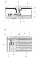
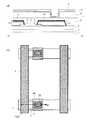
- (A) And (b)is process sectional drawing and a top view for demonstrating an example of the manufacturing method of the semiconductor device 100B, respectively.
- (A) And (b)is process sectional drawing and a top view for demonstrating an example of the manufacturing method of the semiconductor device 100B, respectively.
- (A) And (b)is process sectional drawing and a top view for demonstrating an example of the manufacturing method of the semiconductor device 100B, respectively.
- (A) And (b)is process sectional drawing and a top view for demonstrating an example of the manufacturing method of the semiconductor device 100B, respectively.
- (A) And (b)is process sectional drawing and a top view for demonstrating an example of the manufacturing method of the semiconductor device 100B, respectively,
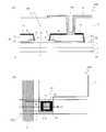
- (c)is an expanded sectional view which shows a contact part.
- FIG. 3is a cross-sectional view illustrating an alignment mark portion 70 in the first embodiment.
- (A) And (b)is sectional drawing and the top view which illustrate the gate terminal part 80 in 1st Embodiment, respectively.
- (A) And (b)is a typical sectional view and a top view of semiconductor device 200A of a 2nd embodiment, respectively.
- (A) And (b)is a typical sectional view and a top view of other semiconductor device 200B of a 2nd embodiment, respectively.
- (A) And (b)is process sectional drawing and a top view for demonstrating an example of the manufacturing method of the semiconductor device 200B, respectively.
- (A) And (b)is process sectional drawing and a top view for demonstrating an example of the manufacturing method of the semiconductor device 200B, respectively.
- (A) And (b)is process sectional drawing and a top view for demonstrating an example of the manufacturing method of the semiconductor device 200B, respectively.
- (A) And (b)is process sectional drawing and a top view for demonstrating an example of the manufacturing method of the semiconductor device 200B, respectively.
- (A) And (b)is process sectional drawing and a top view for demonstrating an example of the manufacturing method of the semiconductor device 200B, respectively.
- (A) And (b)is process sectional drawing and a top view for demonstrating an example of the manufacturing method of the semiconductor device 200B, respectively.
- (A) And (b)is process sectional drawing and a top view for demonstrating an example of the manufacturing method of the semiconductor device 200B, respectively.
- (A) And (b)is a typical sectional view and a top view of semiconductor device 200C in this embodiment, respectively. It is sectional drawing which illustrates the alignment mark part 71 in 2nd Embodiment.
- FIG. 1A) And (b) is sectional drawing and the top view which illustrate the gate terminal part 81 in 2nd Embodiment, respectively. It is sectional drawing which illustrates the semiconductor device 300 of 3rd Embodiment. It is sectional drawing of the conventional oxide semiconductor TFT disclosed by patent document 1.
- FIG. 1A) And (b) is sectional drawing and the top view which illustrate the gate terminal part 81 in 2nd Embodiment, respectively. It is sectional drawing which illustrates the semiconductor device 300 of 3rd Embodiment. It is sectional drawing of the conventional oxide semiconductor TFT disclosed by patent document 1. FIG.
- the “metal oxide film”here does not include a natural oxide film formed on the metal surface. Since the natural oxide film is thin (thickness: less than 5 nm, for example), the influence on the contact resistance is sufficiently smaller than that of the metal oxide film, and the above-described problems are unlikely to occur.
- the “metal oxide film”refers to an oxide film (thickness: for example, 5 nm or more) formed by, for example, an oxidation process on a metal layer or a film formation process such as sputtering. The same applies to “copper oxide film (Cu oxide film)”, “copper alloy oxide film (Cu alloy oxide film)”, or “copper-containing metal oxide film”.
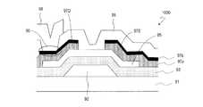
- the source electrode 7S and the drain electrode 7Dinclude a Cu layer (hereinafter referred to as “main layer”) 7a.
- the main layer 7amay be a layer containing Cu as a main component and may contain impurities.
- the source / drain electrode 7may have a laminated structure including the main layer 7a.
- the Cu content in the main layer 7a of the source / drain electrode 7may be, for example, 90% or more.
- the main layer 7ais a pure Cu layer (Cu content: for example, 99.99% or more).
- the surface of the source / drain electrode 7(here, the surface of the Cu layer as the main layer 7a) is exposed to the oxidation treatment when the channel region of the oxide semiconductor layer 5 is oxidized.
- the oxide film formed by doing somay be used.
- the method for forming the Cu oxide film 8is not particularly limited.
- the Cu oxide film 8may be a film formed on the main layer 7a by a film forming process such as sputtering. Even in such a case, by performing chelate cleaning after forming the contact hole CH1, a portion of the Cu oxide film 8 positioned on the bottom surface of the contact hole CH1 can be selectively removed.
- the oxide semiconductor TFT 101 in this embodimentmay have a channel etch structure. If the oxide semiconductor TFT 101 is a channel etch type, a Cu oxide film 8 is formed on the surface of the source / drain electrode 7 simultaneously with the oxidation treatment for the channel region of the oxide semiconductor layer 5.
- the etch stop layeris not formed on the channel region, and the end portions on the channel side of the source electrode 7S and the drain electrode 7D are formed on the oxide semiconductor. It arrange
- the channel etch type TFTis formed, for example, by forming a conductive film for source / drain electrodes on the oxide semiconductor layer 5 and performing source / drain separation. In the source / drain separation step, the surface portion of the channel region may be etched.
- the semiconductor device 100Acan be applied to an active matrix substrate of a display device, for example.
- the semiconductor device 100Acan be applied to a vertical electric field drive display device such as a VA mode.
- the active matrix substratehas a display area (active area) that contributes to display, and a peripheral area (frame area) located outside the display area.
- a plurality of gate lines G and a plurality of source lines Sare formed, and each area surrounded by these lines becomes a “pixel”.
- the plurality of pixelsare arranged in a matrix.
- a transparent conductive layer (pixel electrode) 19is formed in each pixel.
- the pixel electrode 19is separated for each pixel.
- the oxide semiconductor TFT 101is formed in the vicinity of each intersection of the plurality of source lines S and the plurality of gate lines G in each pixel.
- the drain electrode 7 ⁇ / b> D of the oxide semiconductor TFT 101is electrically connected to the corresponding pixel electrode 19.
- the source wiring Smay be formed integrally with the source electrode 7S of the oxide semiconductor TFT 101. That is, the source wiring S includes a main layer 7 a containing Cu as a main component, and even if the Cu oxide film 8 is formed on the upper surface and side surfaces of the source wiring S as well as the source / drain electrodes 7. Good.
- the semiconductor device of this embodimentmay further include another electrode layer functioning as a common electrode on the pixel electrode 19 or between the interlayer insulating layer 11 and the pixel electrode 19. Thereby, a semiconductor device having two transparent electrode layers is obtained. Such a semiconductor device can be applied to an FFS mode display device, for example.
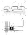
- FIG. 2is a schematic cross-sectional view of another semiconductor device (active matrix substrate) 100B of the present embodiment.
- active matrix substrateactive matrix substrate
- a common signal(COM signal) is applied to the common electrode 15.
- the common electrode 15has an opening 15E for each pixel, and a contact portion between the pixel electrode 19 and the drain electrode 7D of the oxide semiconductor TFT 102 may be formed in the opening 15E (see FIG. 7). .
- the pixel electrode 19 and the drain electrode 7D(main layer 7a) are in direct contact with each other in the contact hole CH1.
- the common electrode 15may be formed over substantially the entire display area (excluding the opening 15E described above).
- the source / drain electrode 7 of the oxide semiconductor TFT 101includes a stacked layer structure including a Cu layer as the main layer 7a and a lower layer (for example, a Ti layer) 7L located on the substrate 1 side of the main layer 7a.
- the lower layer 7Lmay include a metal element such as titanium (Ti) or Mo (molybdenum).
- the lower layer 7Linclude a Ti layer, a Mo layer, a titanium nitride layer, and a molybdenum nitride layer.
- an alloy layer containing Ti or Momay be used.
- the lower layer 7 ⁇ / b> L of the source / drain electrode 7is in contact with the upper surface of the oxide semiconductor layer 5.
- the interlayer insulating layer 11may include a first insulating layer 12 in contact with the oxide semiconductor layer 5 and a second insulating layer 13 formed on the first insulating layer 12.
- the first insulating layer 12may be an inorganic insulating layer
- the second insulating layer 13may be an organic insulating layer.
- the configuration of the semiconductor device having two transparent electrode layersis not limited to the configuration shown in FIG.
- the pixel electrode 19 and the drain electrode 7 ⁇ / b> Dmay be connected via a transparent connection layer formed of the same transparent conductive film as the common electrode 15.
- the transparent connection layeris disposed so as to be in direct contact with the main layer 7a of the drain electrode 7D in the contact hole CH1.
- FIG. 2shows an example in which the common electrode 15 is formed between the interlayer insulating layer 11 and the pixel electrode 19. However, the common electrode 15 is disposed on the pixel electrode 19 via the third insulating layer 17. It may be formed.
- the pixel electrode 19When viewed from the normal direction of the substrate 1, at least a part of the pixel electrode 19 may overlap the common electrode 15 with the third insulating layer 17 interposed therebetween. As a result, a capacitor having the third insulating layer 17 as a dielectric layer is formed in the portion where the pixel electrode 19 and the common electrode 15 overlap.
- This capacitycan function as an auxiliary capacity (transparent auxiliary capacity) in the display device.
- an auxiliary capacitance having a desired capacitancecan be obtained. For this reason, it is not necessary to separately form an auxiliary capacitor in the pixel using, for example, the same metal film as the source wiring. Accordingly, it is possible to suppress a decrease in the aperture ratio due to the formation of the auxiliary capacitor using the metal film.
- the common electrode 15may occupy substantially the entire pixel (other than the opening 15E). Thereby, the area of the auxiliary capacity can be increased.
- the portion of the Cu oxide film 8 located on the bottom surface of the contact hole CH1is preferably removed by chelate cleaning.
- the Cu oxide film 8is formed on the surface of the main layer (Cu layer) 7a by oxidation treatment such as N 2 O plasma treatment.
- the Cu oxide film 8 formed by the oxidation processtends to vary in thickness.
- unevennessmay occur on the surface of the main layer (Cu layer) 7a. Even in such a case, performing chelate cleaning is advantageous because not only the Cu oxide film 8 but also the surface portion of the main layer 7a is removed in the contact hole CH1, and the surface of the main layer 7a can be planarized.
- the interface between the main layer 7a and the transparent conductive layer 19 in the contact portionis the interface between the main layer 7a and the interlayer insulating layer 11 (that is, between the main layer 7a and the interlayer insulating layer 11 via the Cu oxide film 8). It becomes flatter than the interface.
- the contact resistance between the drain electrode 7D and the transparent conductive layer 19can be significantly reduced.
- the reliabilitycan be improved.
- the adhesion of the transparent conductive layer 19 to the drain electrode 7Dcan be more effectively enhanced.
- the part located in the bottom face of contact hole CH1when planarized by chelate cleaning among the surfaces of drain electrode 7D, it may be located below other parts covered with Cu oxide film 8.
- the etching of the Cu oxide film 8may proceed in the lateral direction (side etching). In this case, when viewed from the normal direction of the substrate 1, the end of the Cu oxide film 8 is located outside the contour of the contact hole CH 1 (the end of the interlayer insulating layer 11).
- FIG. 3 to 11are views for explaining an example of the manufacturing method of the semiconductor device 100B.
- FIG. 3Ais a cross-sectional view taken along the line II ′ in FIG. Shows a plan view.
- a gate electrode 3, a gate wiring G, a gate insulating layer 4, and an oxide semiconductor layer 5are formed in this order on a substrate 1.
- the substratefor example, a glass substrate, a silicon substrate, a heat-resistant plastic substrate (resin substrate), or the like can be used.
- the gate electrode 3can be formed integrally with the gate wiring G.
- a metal film for gate wiring(thickness: for example, 50 nm to 500 nm) (not shown) is formed on the substrate (for example, glass substrate) 1 by sputtering or the like.
- the gate electrode 3 and the gate wiring Gare obtained by patterning the metal film for gate wiring.
- the gate wiring metal filmfor example, a laminated film (Cu / Ti film) having Cu as an upper layer and Ti as a lower layer is used.
- the material for the metal film for gate wiringis not particularly limited.
- a film containing a metalsuch as aluminum (Al), tungsten (W), molybdenum (Mo), tantalum (Ta), chromium (Cr), titanium (Ti), copper (Cu), or an alloy thereof, or a metal nitride thereof It can be used as appropriate.
- a metalsuch as aluminum (Al), tungsten (W), molybdenum (Mo), tantalum (Ta), chromium (Cr), titanium (Ti), copper (Cu), or an alloy thereof, or a metal nitride thereof It can be used as appropriate.
- the gate insulating layer 4can be formed by a CVD method or the like.
- a silicon oxide (SiO 2 ) layer, a silicon nitride (SiNx) layer, a silicon oxynitride (SiOxNy; x> y) layer, a silicon nitride oxide (SiNxOy; x> y) layer, or the likeis appropriately used.
- the gate insulating layer 4may have a stacked structure.
- an oxide semiconductor film(thickness: for example, 30 nm or more and 200 nm or less) is formed on the gate insulating layer 4 by using, for example, a sputtering method. Thereafter, the oxide semiconductor film is patterned by photolithography to obtain the oxide semiconductor layer 5.
- the oxide semiconductor layer 5is disposed so as to overlap the gate electrode 3 with the gate insulating layer 4 interposed therebetween.
- an oxide semiconductor layeris formed by patterning an In—Ga—Zn—O-based amorphous oxide semiconductor film (thickness: for example, 50 nm) containing In, Ga, and Zn at a ratio of 1: 1: 1. 5 is formed.
- the oxide semiconductor layer 5may have a stacked structure of two or more layers.
- the oxide semiconductor layer 5may include an amorphous oxide semiconductor layer and a crystalline oxide semiconductor layer. Alternatively, a plurality of crystalline oxide semiconductor layers having different crystal structures may be included.
- the energy gap of the oxide semiconductor included in the upper layeris preferably larger than the energy gap of the oxide semiconductor included in the lower layer. However, when the difference in energy gap between these layers is relatively small, the energy gap of the lower oxide semiconductor may be larger than the energy gap of the upper oxide semiconductor.
- the oxide semiconductor layer 5may include at least one metal element of In, Ga, and Zn, for example.
- the oxide semiconductor layer 5includes, for example, an In—Ga—Zn—O-based semiconductor.
- Such an oxide semiconductor layer 5can be formed of an oxide semiconductor film containing an In—Ga—Zn—O-based semiconductor.
- a channel-etch TFT having an active layer containing an In—Ga—Zn—O-based semiconductormay be referred to as a “CE-InGaZnO-TFT”.
- the In—Ga—Zn—O-based semiconductormay be amorphous or crystalline.
- a crystalline In—Ga—Zn—O-based semiconductor in which the c-axis is oriented substantially perpendicular to the layer surfaceis preferable.
- a TFT having an In—Ga—Zn—O-based semiconductor layerhas high mobility (more than 20 times that of an a-Si TFT) and low leakage current (less than one hundredth of that of an a-Si TFT). It is suitably used as a drive TFT and a pixel TFT.
- the oxide semiconductor layer 5may include another oxide semiconductor instead of the In—Ga—Zn—O-based semiconductor.
- an In—Sn—Zn—O-based semiconductoreg, In 2 O 3 —SnO 2 —ZnO
- the In—Sn—Zn—O-based semiconductoris a ternary oxide of In (indium), Sn (tin), and Zn (zinc).
- the oxide semiconductor layer 5includes an In—Al—Zn—O based semiconductor, an In—Al—Sn—Zn—O based semiconductor, a Zn—O based semiconductor, an In—Zn—O based semiconductor, and a Zn—Ti—O semiconductor.
- Cd—Ge—O semiconductorCd—Pb—O semiconductor, CdO (cadmium oxide), Mg—Zn—O semiconductor, In—Ga—Sn—O semiconductor, In—Ga—O semiconductor
- a Zr—In—Zn—O based semiconductoran Hf—In—Zn—O based semiconductor, or the like may be included.
- a source / drain electrode 7 including a Cu layer as the main layer 7ais formed so as to be in contact with the upper surface of the oxide semiconductor layer 5.
- the source / drain electrode 7only needs to have a main layer 7a mainly containing Cu, and may have a single layer structure or a laminated structure including a Cu layer and other conductive layers. Also good.
- a source wiring metal film(thickness: for example, 50 nm to 500 nm) is formed on the gate insulating layer 4 and the oxide semiconductor layer 5.
- a laminated film in which a Ti film and a Cu film are stacked in this order from the oxide semiconductor layer 5 sideis formed as the source wiring metal film.
- a Cu filmmay be formed as the source wiring metal film.
- the source wiring metal filmis formed by, for example, sputtering.
- the Cu filmmay be a film containing Cu as a main component and may contain impurities. A pure Cu film is preferable.
- the source electrode 7S, the drain electrode 7D, and the source wiring Shave a laminated structure including a lower layer (here, Ti layer) 7L and a main layer (here, Cu layer) 7a disposed on the lower layer 7L.
- the main layer 7aconstitutes the upper surfaces of the source electrode 7S and the drain electrode 7D.
- the lower layer 7 ⁇ / b> Lis in contact with the oxide semiconductor layer 5.
- the source / drain electrode 7has, for example, a lower layer 7L containing a metal element such as titanium (Ti) or Mo (molybdenum) on the substrate 1 side of the main layer 7a.
- a metal elementsuch as titanium (Ti) or Mo (molybdenum)
- the lower layer 7Linclude a Ti layer, a Mo layer, a titanium nitride layer, and a molybdenum nitride layer.
- an alloy layer containing Ti or Momay be used.
- the oxidation treatmentis not limited to plasma treatment using N 2 O gas.
- the oxidation treatmentcan be performed by plasma treatment using O 2 gas, ozone treatment, or the like.
- the N 2 O plasma treatmentmay be performed, and when the interlayer insulating layer 11 is formed by the sputtering method, the O 2 plasma processing may be performed.
- the oxidation treatmentmay be performed by O 2 plasma treatment in an ashing apparatus.
- an interlayer insulating layer 11is formed so as to cover the oxide semiconductor TFT 101.
- Interlayer insulating layer 11is arranged in contact with Cu oxide film 8 and channel region 5c.
- the first insulating layer 12is an inorganic material such as a silicon oxide (SiO 2 ) film, a silicon nitride (SiNx) film, a silicon oxynitride (SiOxNy; x> y) film, or a silicon nitride oxide (SiNxOy; x> y) film.
- An insulating layermay be used.
- a SiO 2 layer having a thickness of, eg, 200 nmis formed by, eg, CVD.
- the second insulating layer 13may be, for example, an organic insulating layer.
- a positive photosensitive resin film having a thickness of, for example, 2000 nmis formed, and the photosensitive resin film is patterned.
- an opening 13E exposing the first insulating layer 12is formed in a portion located above the drain electrode 7D.
- the material of these insulating layers 12 and 13is not limited to the said material.
- the second insulating layer 13may be an inorganic insulating layer.
- an ITO (indium tin oxide) film(thickness: 50 nm or more and 200 nm or less), an IZO film, a ZnO film (zinc oxide film), or the like can be used.
- an ITO film having a thickness of, for example, 100 nmis used as the transparent conductive film.
- the resist maskis removed using a resist stripping solution (for example, an amine-based stripping solution).
- a resist stripping solutionfor example, an amine-based stripping solution.
- the surface of the main layer 7a after the oxidation treatmentmay have unevenness due to variations in the thickness of the Cu oxide film 8. This surface unevenness is not reduced by the resist mask stripping solution. Therefore, it is difficult to obtain a good contact even if it is brought into contact with the transparent conductive layer in this state.
- the Cu oxide film 8is not disposed on a portion of the upper surface of the drain electrode 7 ⁇ / b> D that overlaps the opening of the first insulating layer 12. A portion of the Cu oxide film 8 located at the interface between the interlayer insulating layer 11 and the source / drain electrodes 7 and the source wiring S remains without being removed.
- chelate cleaning solutionfor example, a mixed solution containing a hydrogen peroxide solution, a basic chemical solution, and water (main component) can be used.
- the basic chemical solutionmay be TMAH (tetramethylammonium hydroxide), for example.
- the temperature of the cleaning liquidmay be, for example, 30 to 40 ° C., and the cleaning time may be, for example, about 60 to 90 seconds.
- FIG. 10Cis a diagram schematically showing an example of a cross-sectional structure of the substrate 1 after chelate cleaning.
- the Cu oxide film 8may be etched (side-etched) in the lateral direction (direction parallel to the substrate 1) by chelate cleaning.
- the end portion P (10) of the Cu oxide film 8 in the contact hole CH 1is more than the end portion P (CH) of the interlayer insulating layer 11. It is located outside by ⁇ x).
- the end portion of the Cu oxide film 8is positioned so as to surround the opening portion 17 ⁇ / b> E of the interlayer insulating layer 11.
- a transparent conductive film(not shown) is formed, for example, by sputtering in the contact hole CH1 and on the third insulating layer 17, and is patterned.
- the transparent conductive layer 19is formed.
- the transparent conductive layer 19has a comb-shaped planar shape having a plurality of cuts.
- the transparent conductive layer 19is in direct contact with the main layer 7a of the drain electrode 7D in the contact hole CH1. In this way, the semiconductor device 100B is manufactured.
- the transparent conductive film for forming the transparent conductive layer 19for example, an ITO (indium tin oxide) film (thickness: 50 nm or more and 150 nm or less), an IZO film, a ZnO film (zinc oxide film), or the like is used. It can.
- an ITO film having a thickness of, for example, 100 nmis used as the transparent conductive film.
- the two-layer electrode structure having the pixel electrode as the upper layeris formed.
- the transparent conductive layer 19 functioning as the pixel electrodeis used as the lower layer, and the common electrode 15 is formed thereon via the third insulating layer 17.
- the interlayer insulating layer 11is formed, and then the first insulating layer 12 is etched using the second insulating layer 13 as a mask, thereby forming the contact hole CH1.
- the Cu oxide film 8 located on the bottom surface of the contact hole CH1is removed by chelate cleaning to expose the Cu surface.
- the transparent conductive layer 19is formed in the contact hole CH1 and on the second insulating layer 13.
- the transparent conductive layer 19can be provided so as to be in direct contact with the drain electrode 7D in the contact hole CH1.
- an inorganic insulating layerthickness: for example, a silicon oxide (SiO 2 ) layer, a silicon nitride (SiNx) layer, a silicon oxynitride (SiOxNy; x> y) layer, a silicon nitride oxide (SiNxOy; x> y) layer, or the like 200 nm).
- Such an inorganic insulating layercan be formed by, for example, a CVD method.
- the interlayer insulating layer 11may have a laminated structure including, for example, a SiO 2 layer and a SiNx layer.
- the oxide semiconductor layer 5(channel region 5 c) is disposed so as to overlap the gate electrode 3 with the gate insulating layer 4 interposed therebetween.
- the oxide semiconductor TFT 101may be disposed so as to overlap the gate electrode (gate wiring) 3 as a whole.
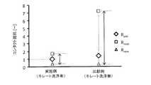
- the semiconductor device 100Bwas manufactured by the method described above. Further, as a comparative example, a semiconductor device was manufactured by the same method as described above except that chelate cleaning was not performed after the formation of the contact hole CH1.
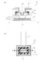
- FIG. 12is a diagram illustrating a cross-sectional SEM image of the contact portion between the drain electrode 7D and the transparent conductive layer 19 in the semiconductor device of the example.
- the unevenness of the interface (contact surface) 21 between the main layer 7a of the drain electrode 7D and the transparent conductive layer 19causes the interface between the main layer 7a and the interlayer insulating layer 11 (here, the first insulating layer 12) (that is, Cu oxidation).
- the unevenness at the interface between the main layer 7a and the interlayer insulating layer 11 via the film 8is smaller. From this, it can be seen that the irregularities generated in the portion of the Cu surface that becomes the contact surface 21 in the oxidation treatment step are reduced and flattened by chelate cleaning.
- the average value Rave of the contact resistancecan be reduced in the semiconductor device of the example in which chelate cleaning is performed, as compared with the semiconductor device of the comparative example.
- the Cu oxide film 8remains in the contact hole CH1 and is interposed between the drain electrode 7D and the transparent conductive layer 19, whereas in the embodiment, it is located in the contact hole CH1 by chelate cleaning. This is probably because the Cu oxide film 8 to be removed has been removed.
- the minimum value Rmin of the contact resistanceis approximately the same. From this, in the semiconductor device of the comparative example, as a result of removing a part (surface portion) of the Cu oxide film 8 in the contact hole CH1 with the stripping solution in a part of the contact portions by the stripping solution of the resist mask. There is a possibility that the Cu oxide film 8 has been thinned to such an extent that the contact resistance can be ignored. However, it is difficult to uniformly and sufficiently thin the Cu oxide film 8 in the contact hole CH1 over the entire substrate 1 with the resist mask stripping solution. For this reason, for example, there is a contact portion having a contact resistance of 5 times or more of the average value Rave. On the other hand, in the semiconductor device of the embodiment, the Cu oxide film 8 in the contact hole CH1 can be removed over the entire substrate 1. Variations in contact resistance can be suppressed to about 25% or less, for example.
- an alignment markmay be provided on the substrate for mask alignment.
- the alignment markis formed using, for example, the same conductive film (source wiring layer) as the source / drain electrode 7.
- the alignment markis read based on, for example, the reflectance when light is irradiated.
- the alignment mark part 70has, for example, a mark layer 7 m formed using the same conductive film as the source / drain electrode 7.
- the mark layer 7mhas a main layer 7a mainly composed of Cu. You may have a lower layer in the board
- An interlayer insulating layer 11is extended on the mark layer 7m.
- the interlayer insulating layer 11has an opening H on at least a part of the upper surface of the mark layer 7m. In this example, the opening H is disposed so as to expose the entire upper surface of the mark layer 7m.
- the interlayer insulating layer 11is in contact with the side surface of the mark layer 7 m through the Cu oxide film 8.
- a Cu oxide film 8is not formed on a portion of the mark layer 7m exposed by the opening H, that is, a portion overlapping the opening H on the upper surface of the mark layer 7m when viewed from the normal direction of the substrate 1.
- the main layer 7ais exposed.
- the alignment mark portion 70can be formed by a process common to the method described above with reference to FIGS. Specifically, after the mark layer 7m is formed by patterning the metal film for source wiring, the upper surface and the side surface of the mark layer 7m are oxidized in the oxidation process for the oxide semiconductor layer 5, and the Cu oxide film 8 is formed. The Next, after forming the interlayer insulating layer 11, an opening H is formed on the mark layer 7 m in the patterning process of the interlayer insulating layer 11. Thereafter, when the Cu oxide film 8 in the contact hole CH1 is removed by chelate cleaning, the Cu oxide film 8 in the opening H is also removed. The opening H may be arranged so as to expose the entire mark layer 7m. In that case, the Cu oxide film 8 on the upper surface and side surfaces of the mark layer 7m can all be removed by chelate cleaning.
- the end of the Cu oxide film 8when viewed from the normal direction of the substrate 1, the end of the Cu oxide film 8 has an opening H. It may be located outside the end of the defined interlayer insulating layer 11.
- At least one alignment mark portion 70 described aboveis formed on the substrate 1.
- the alignment mark part 70may be formed as it is on the substrate 1 of the semiconductor devices 100A and 100B after the product is completed, or may be separated and removed before the product is completed.
- the wiring layer including the source / drain electrodes 7may have the above-described stacked structure.
- the surface (upper surface and side surface) of the source wiring layermay be covered with the Cu oxide film 8.
- the Cu oxide film 8is removed as in the contact portion between the drain electrode 7D and the transparent conductive layer 19 described above. It is preferable. Thereby, an increase in contact resistance can be suppressed.
- a source connection layer formed integrally with the source wiring S and an upper conductive layer formed of the same film as the transparent conductive layer 19are provided in the interlayer insulating layer 11. You may provide the source terminal part connected within a contact hole. In the source terminal portion, the Cu oxide film 8 formed on the upper surface of the source connection layer is removed in the contact hole of the interlayer insulating layer 11, and the source connection layer and the upper conductive layer are in the contact hole of the interlayer insulating layer 11. Direct contact is preferred.
- a gate terminal portionthat connects a gate connection layer formed integrally with the gate wiring G and an upper conductive layer formed of the same film as the transparent conductive layer 19 may be provided.
- the gate connection layer and the upper conductive layermay be connected via a source connection layer formed from the same film as the source wiring S in a contact hole provided in the interlayer insulating layer 11.
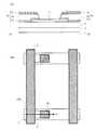
- FIGS. 15A and 15Bare a cross-sectional view and a plan view illustrating the gate terminal portion, respectively. Components similar to those in FIG. 1 are denoted by the same reference numerals.
- FIG. 15Ashows a cross section taken along the line II-II ′ in FIG.
- the gate terminal portion 80extends on the gate connection layer 3t formed on the substrate 1, the gate insulating layer 4 extending on the gate connection layer 3t, the source connection layer 7t, and the source connection layer 7t.
- the interlayer insulating layer 11 and the upper conductive layer 19tare provided.
- the source connection layer 7tis formed of the same conductive film as the source wiring S and is electrically isolated from the source wiring S.
- the source connection layer 7tis disposed in the opening provided in the gate insulating layer 4 so as to be in contact with the gate connection layer 3t.
- the upper conductive layer 19tis disposed in the contact hole CH2 provided in the interlayer insulating layer 11 so as to be in contact with the source connection layer 7t.
- the source connection layer 7tincludes a Cu layer, and a part of the upper surface of the source connection layer 7t is covered with a Cu oxide film 8.
- the Cu oxide film 8is also disposed on the side surface of the source connection layer 7t.
- the Cu oxide film 8is removed, and the upper conductive layer 19t and the upper surface (Cu surface) of the source connection layer 7t are in direct contact with each other. That is, the Cu oxide film 8 is interposed between the source connection layer 7t and the interlayer insulating layer 11, and is not interposed between the source connection layer 7t and the upper conductive layer 19t. This makes it possible to reduce the contact resistance between the gate connection layer 3t and the upper conductive layer 19t.
- the gate terminal portion 80can be manufactured as follows. First, a source wiring layer including the gate connection layer 3t, the gate insulating layer 4, the oxide semiconductor layer (not shown), and the source connection layer 7t is formed. The source connection layer 7t is disposed in contact with the gate connection layer 3t in the opening of the gate insulating layer 4. Next, oxidation treatment of the oxide semiconductor layer is performed. At this time, the surface (Cu surface) of the source connection layer 7t is oxidized, and the Cu oxide film 8 is formed. Subsequently, an interlayer insulating layer 11 covering the source wiring layer is formed, and a contact hole CH2 exposing the Cu oxide film 8 is provided in the interlayer insulating layer 11. Next, the portion of the Cu oxide film 8 exposed by the contact hole CH2 is removed by chelate cleaning or the like. Thereafter, an upper conductive layer 19t is provided in the contact hole CH2 so as to be in contact with the source connection layer 7t.
- the semiconductor devices 100A and 100Binclude a source-gate connection layer that connects the source line S and the gate line G via a conductive layer formed of the same film as the transparent conductive layer 19. May be. Also in the source-gate connection layer, the Cu oxide film 8 on the source wiring S is removed in the contact hole provided in the interlayer insulating layer 11 as described above, and the source wiring S and the conductive layer are in direct contact with each other. Also good.
- the semiconductor device of this embodimentis different from that of the first embodiment in that a Cu alloy oxide film is formed on the surface of the source and drain electrodes.
- FIGS. 16A and 16Bare a schematic cross-sectional view and a plan view of the semiconductor device 200A of the present embodiment, respectively.
- FIG. 16Ashows a cross section taken along line III-III ′ in FIG. In FIG. 16, the same components as those in FIG.
- the oxide semiconductor TFT 201includes a gate electrode 3 supported on the substrate 1, a gate insulating layer 4 covering the gate electrode 3, and an oxide semiconductor layer disposed so as to overlap the gate electrode 3 with the gate insulating layer 4 interposed therebetween. 5, a source electrode 7 ⁇ / b> S and a drain electrode 7 ⁇ / b> D (source / drain electrode 7), and a Cu alloy oxide film 10 disposed on the upper surface of the source / drain electrode 7.
- the source / drain electrode 7 in this embodimentincludes a main layer 7a containing Cu as a main component and an upper layer 7U provided on the main layer 7a.
- the upper layer 7Ucontains a Cu alloy.
- the source / drain electrode 7may have a lower layer 7L disposed on the substrate 1 side of the main layer 7a.
- the lower layer 7 ⁇ / b> Lmay be disposed so as to be in contact with the oxide semiconductor layer 5.
- the lower layer 7Lmay contain, for example, titanium (Ti) or molybdenum (Mo).
- the interlayer insulating layer 11is disposed so as to be in contact with the channel region 5 c of the oxide semiconductor layer 5.
- the interlayer insulating layer 11is disposed so as to cover the source electrode 7S and the drain electrode 7D with the Cu alloy oxide film 10 interposed therebetween.
- a contact hole CH1 reaching the surface of the drain electrode 7D(here, the surface of the upper layer 7U) is formed.
- the Cu alloy oxide film 10is not disposed on the bottom surface of the contact hole CH1, and the surface of the drain electrode 7D is exposed.
- the transparent conductive layer 19is provided on the interlayer insulating layer 11 and in the contact hole CH1.
- the transparent conductive layer 19is in direct contact with the drain electrode 7D (here, the upper layer 7U) without the Cu alloy oxide film 10 in the contact hole CH1.
- the transparent conductive layer 19is, for example, a pixel electrode.
- the total ratio thereofmay be, for example, 0 at% or more and 20 at% or less. Thereby, the oxidation of Cu can be suppressed more reliably.
- the Cu alloyfor example, CuMgAl (Mg: 0 to 10 at%, Al: 0 to 10 at%), CuCa (Ca: 0 to 10 at%), or the like can be used.
- the common electrode 15has an opening 15E for each pixel, and a contact portion between the pixel electrode 19 and the drain electrode 7D of the oxide semiconductor TFT 201 may be formed in the opening 15E.
- the pixel electrode 19 and the upper layer 7U of the drain electrode 7Dare in direct contact with each other without the Cu alloy oxide film 10 in the contact hole CH1.
- the pixel electrode 19 and the drain electrode 7Dmay be connected by a transparent connection layer formed of the same conductive film (transparent conductive film) as the common electrode 15. In this case, the transparent connection layer and the upper layer 7U of the drain electrode 7D are in direct contact with each other in the contact hole CH1.
- the common electrode 15may be disposed on the pixel electrode 19 via the third insulating layer 17.
- the pixel electrode 19when viewed from the normal direction of the substrate 1, at least a part of the pixel electrode 19 may overlap the common electrode 15 with the third insulating layer 17 interposed therebetween. As a result, a capacitor having the third insulating layer 17 as a dielectric layer is formed in the portion where the pixel electrode 19 and the common electrode 15 overlap. Further, instead of the common electrode 15, a transparent conductive layer that functions as an auxiliary capacitance electrode may be provided to face the pixel electrode 19 to form a transparent auxiliary capacitance in the pixel. Such a semiconductor device can also be applied to a display device in an operation mode other than the FFS mode.
- the transparent conductive layer 19is in direct contact with the drain electrode 7D (here, the upper layer 7U) without the Cu alloy oxide film 10 in the contact hole CH1.
- the same effect as described above with reference to FIGS. 12 and 13can be obtained by performing chelate cleaning.
- the Cu alloy oxide film 10 formed by oxidation treatmenttends to vary in thickness. For this reason, irregularities may occur at the interface between the drain electrode 7D and the Cu alloy oxide film 10.
- by performing chelate cleaningnot only the Cu alloy oxide film 10 but also the surface portion of the drain electrode 7D (here, the upper layer 7U) is removed in the contact hole CH1, and the surface of the drain electrode 7D is thus removed. Can be flattened.
- the interface between the drain electrode 7D and the transparent conductive layer 19is the interface between the drain electrode 7D (upper layer 7U) and the interlayer insulating layer 11 (that is, the drain electrode 7D and the interlayer insulating layer 11 via the Cu alloy oxide film 10). Flatter than the interface).
- the contact resistance between the drain electrode 7D and the transparent conductive layer 19can be significantly reduced.
- the reliabilitycan be improved.
- the adhesion of the transparent conductive layer 19 to the drain electrode 7Dcan be more effectively enhanced.
- the part located in the bottom face of contact hole CH1when planarized by chelate cleaning among the surfaces of drain electrode 7D, it may be located below other parts covered with Cu alloy oxide film 10. . Further, when the Cu alloy oxide film 10 is removed by chelate cleaning, the etching of the Cu alloy oxide film 10 may proceed in the lateral direction (side etching). In this case, when viewed from the normal direction of the substrate 1, the end of the Cu alloy oxide film 10 is located outside the contour of the contact hole CH 1 (the end of the interlayer insulating layer 11).
- the semiconductor devices 200A and 200Bhave the following merits compared to the embodiment (semiconductor devices 100A and 100B) in which the Cu oxide film 8 is provided on the upper surface of the source / drain electrode 7.
- an upper layer 7U containing a Cu alloyis formed on the main layer 7a.
- the oxidation of Cuis less likely to proceed during the oxidation process. This is because not only Cu but also metal elements added to Cu are oxidized during the oxidation treatment. When a metal element that oxidizes more easily than Cu is contained, oxidation of Cu can be more effectively suppressed. As a result, the corrosion of the electrode resulting from the oxidation of Cu can be effectively suppressed. Further, high adhesion to the interlayer insulating layer 11 can be ensured.
- the thickness of the Cu alloy oxide film 10 obtained by oxidizing the Cu alloy surfaceis smaller than the thickness of the Cu oxide film obtained by oxidizing the Cu surface. For this reason, the unevenness
- the Cu alloy oxide film 10can be more easily removed, and the side etch amount of the Cu alloy oxide film 10 can be reduced.
- the upper surface (Cu surface) of the alignment markmay be oxidized and discolored, resulting in poor alignment mark reading.
- the Cu alloy oxide film 10is formed on the upper surface of the alignment mark, the above-described discoloration does not occur. Therefore, an alignment mark having high discrimination can be formed.
- the manufacturing method of the semiconductor device of the present embodimentwill be described by taking the manufacturing method of the semiconductor device 200B as an example. Note that description of the material, thickness, and formation method of each layer in the semiconductor device 200B will be omitted in the same manner as the material, thickness, and formation method of each layer in the semiconductor devices 100A and 100B.
- FIG. 18 to 24are views for explaining an example of the manufacturing method of the semiconductor device 200B.
- FIG. 18Ais a cross-sectional view taken along the line III-III ′
- FIG. 18Bis a plan view. Show.
- the thickness of the Cu alloy film that forms the upper layer 7Uis preferably 10 nm or more and 100 nm or less. If it is 10 nm or more, a Cu alloy oxide film capable of sufficiently suppressing the oxidation of Cu can be formed in a later step. Note that the thickness of the upper layer 7U at the time of product completion is smaller than the thickness at the time of film formation by the amount used for forming the Cu alloy oxide film 10.
- the exposed side surfaces of the source / drain electrodes 7are also oxidized by the oxidation process.
- the Ti oxide film 9can be formed on the side surface of the lower layer 7L
- the Cu oxide film 8can be formed on the side surface of the main layer 7a
- the Cu alloy oxide film 10can be formed on the side surface of the upper layer 7U.
- the thickness of the Cu oxide film 8is larger than the thickness of the Cu alloy oxide film 10, for example, 20 nm.
- the thickness of the Ti oxide film 9is smaller than the thickness of the Cu alloy oxide film 10.
- the Cu alloy oxide film 10 located in the contact hole CH1is removed.
- the Cu alloy oxide film 10is removed by a cleaning process using a chelate cleaning solution.
- the cleaning solution and conditions used for chelate cleaningmay be the same as those in the above-described embodiment.
- the surface of the drain electrode 7Dthat is, the surface of the upper layer 7U
- a portion of the Cu alloy oxide film 10 located at the interface between the interlayer insulating layer 11 and the source / drain electrodes 7 and the source wiring Sremains without being removed.
- the Cu alloy oxide film 10is etched (side-etched) in the lateral direction (direction parallel to the substrate 1) by chelate cleaning. There is. In this case, when viewed from the normal direction of the substrate 1, the end portion of the Cu alloy oxide film 10 is positioned outside the end portion (end portion of the opening) of the interlayer insulating layer 11 in the contact hole CH ⁇ b> 1. Also, as described above with reference to FIG. 12, in this embodiment as well, not only the Cu alloy oxide film 10 but also a part of the surface portion (Cu) of the main layer 7a may be removed by chelate cleaning. . Thereby, the unevenness generated on the surface of the upper layer 7U by the oxidation treatment is reduced, and the contact surface is flattened.
- the two-layer electrode structure having the pixel electrode as the upper layeris formed.
- the transparent conductive layer 19 functioning as the pixel electrodeis used as the lower layer, and the common electrode 15 is formed thereon via the third insulating layer 17.
- the first insulating layer 12is etched (wet etching) using the second insulating layer 13 as a mask to form the contact hole CH1.
- the Cu alloy oxide film 10 located on the bottom surface of the contact hole CH1may be removed by chelate cleaning to expose the Cu alloy surface.
- a contact hole CH1is formed in a portion of the interlayer insulating layer 11 located on the drain electrode 7D, and the contact hole CH1 is formed.
- the Cu alloy oxide film 10may be exposed on the bottom surface of.
- an inorganic insulating layeris formed as the interlayer insulating layer 11
- a resist maskmay be provided on the inorganic insulating layer, and the contact hole CH1 may be formed in the interlayer insulating layer 11 using the resist mask.
- the contact hole CH1may be formed by etching the first insulating layer 12 using the second insulating layer 13 as a mask. After the formation of the contact hole CH1, chelate cleaning can be performed to expose the Cu alloy surface.
- the resist maskis not peeled off, so the Cu alloy oxide film 10 located on the bottom surface of the contact hole CH1 is not thinned with the resist stripping solution.
- the contact resistancecan be more effectively reduced by removing the Cu alloy oxide film 10 by performing chelate cleaning.
- FIGS. 25A and 25Bare a schematic cross-sectional view and a plan view, respectively, of the semiconductor device 200C in the present embodiment.
- FIG. 25Ashows a cross section taken along the line IV-IV ′ in FIG.
- the same components as those in FIG. 16are denoted by the same reference numerals, and description thereof is omitted.
- the semiconductor device 200Cdiffers from the semiconductor device 200A shown in FIG. 16 in that the source / drain electrode 7 constituting the oxide semiconductor TFT 201 is not provided with a Cu alloy layer on the main layer 7a.
- the Cu alloy oxide film 10is disposed on the main layer 7a.
- the Cu alloy oxide film 10may be formed, for example, in contact with the upper surface of the main layer 7a.
- the Cu alloy oxide film 10may be a sputtered film, for example.
- a Cu oxide film 8 and a metal oxide film 9are arranged on the side surfaces of the main layer 7a and the lower layer 7L, respectively. Further, the Cu alloy oxide film 10 is removed in the contact hole CH1, and the transparent conductive layer 19 is in direct contact with the main layer 7a of the drain electrode 7D.
- Other configurationsare the same as those of the above-described embodiment.
- the semiconductor device 200Ccan be manufactured, for example, as follows. First, the gate electrode 3, the gate insulating layer 4, and the oxide semiconductor layer 5 are formed by a method similar to that of the semiconductor devices 200A and 200B. Next, a metal film for source wiring is formed by sputtering, for example. Here, a metal film (for example, Ti film) serving as a lower layer and a Cu film serving as a main layer are formed in this order. Thereafter, a Cu alloy oxide film 10 is formed on the source wiring metal film. The Cu alloy oxide film 10 may be formed by sputtering using a Cu alloy target in an atmosphere containing oxygen (for example, an Ar / O 2 atmosphere). Thereafter, using the same mask, the metal film for source wiring and the Cu alloy oxide film 10 are patterned to obtain the source / drain electrodes 7 and the source wiring S. The upper surfaces of these electrodes / wirings are covered with a Cu alloy oxide film 10.
- a metal film for source wiringis formed by sputtering, for example.
- an interlayer insulating layer 11is formed, a contact hole CH1 is formed in the interlayer insulating layer 11, and the Cu alloy oxide film 10 is exposed.
- the portion of the Cu alloy oxide film 10 located on the bottom surface of the contact hole CH1is removed by chelate cleaning, and the surface of the drain electrode 7D (here, the surface of the main layer 7a) is exposed.
- a transparent conductive layer 19is provided on the interlayer insulating layer 11 and in the contact hole CH1 so as to be in contact with the drain electrode 7D. In this way, the semiconductor device 200C is manufactured.
- the Cu alloy oxide film 10is disposed between the source / drain electrode 7 and the interlayer insulating layer 11 and is not disposed on the contact surface between the main layer 7 a and the transparent conductive layer 19. For this reason, it is possible to suppress deterioration in device characteristics due to an increase in contact resistance between the drain electrode 7D and the transparent conductive layer 19 while suppressing oxidation / discoloration of the main layer (Cu layer) 7a.
- the upper surface of the source wiring layeris covered with the Cu alloy oxide film 10 and Cu oxidation is suppressed, electrode corrosion due to Cu oxidation and discoloration, poor alignment mark reading, and the like can be reduced.
- alignment marksmay be provided on the substrate 1 for mask alignment.
- the alignment markis formed using, for example, the same conductive film (source wiring layer) as the source / drain electrode 7.
- the alignment markis read based on, for example, the reflectance when light is irradiated.
- FIG. 26is a cross-sectional view showing an example of the alignment mark portion 71 used in the present embodiment.
- FIGS. 27A and 27Bare a cross-sectional view and a plan view illustrating the gate terminal portion, respectively. Components similar to those in FIG. 1 are denoted by the same reference numerals.
- FIG. 27Ashows a cross section taken along the line V-V ′ in FIG.
- the gate terminal portion 81extends on the gate connection layer 3t formed on the substrate 1, the gate insulating layer 4 extending on the gate connection layer 3t, the source connection layer 7t, and the source connection layer 7t. And an upper conductive layer 19t formed in the contact hole CH2 formed in the interlayer insulating layer 11.
- the source connection layer 7tis formed of the same conductive film as the source wiring S and is electrically isolated from the source wiring S.
- the source connection layer 7tincludes a Cu layer and a Cu alloy layer disposed on the Cu layer.
- a Cu alloy oxide film 10is disposed on the upper surface of the source connection layer 7t.
- a Cu alloy oxide film 10is disposed on the side surface of the Cu alloy layer in the source connection layer 7t, and a Cu oxide film 8 is disposed on the side surface of the Cu layer.
- the Cu alloy oxide film 10is removed, and the upper conductive layer 19t and the upper surface (Cu alloy surface) of the source connection layer 7t are in direct contact with each other. That is, the Cu alloy oxide film 10 is interposed between the source connection layer 7t and the interlayer insulating layer 11, and is not interposed between the source connection layer 7t and the upper conductive layer 19t. This makes it possible to reduce the contact resistance between the gate connection layer 3t and the upper conductive layer 19t.
- FIG. 28is a cross-sectional view illustrating a semiconductor device 300 of this embodiment.
- the oxide semiconductor TFT 301 in the semiconductor device 300has a Cu alloy layer 7 b as a main layer of the source / drain electrode 7.
- a Cu alloy oxide film 10is formed between the source / drain electrodes 7 and the interlayer insulating layer 11.
- the contact hole CH1 provided in the interlayer insulating layer 11the Cu alloy oxide film 10 is removed, and the transparent conductive layer 19 is in direct contact with the Cu alloy layer 7b.
- Other configurationsare similar to those of the semiconductor device 100A.
- the Cu alloy layer 7bonly needs to contain a Cu alloy, and may contain impurities.
- an additive metal element of the Cu alloya metal element having a property that is easier to oxidize than Cu may be included.
- the additive metal elementmay include at least one metal element selected from the group consisting of Mg, Al, Ca, Ti, Mo, and Mn. Thereby, the oxidation of Cu can be suppressed more effectively.
- the ratio of the additive metal element to the Cu alloy(the ratio of each additive metal element when two or more additive metal elements are included) is the same as the ratio of the additive metal element of the upper layer 7U in the second embodiment described above. May be.
- the Cu alloy oxide film 10is disposed between the source / drain electrode 7 and the interlayer insulating layer 11, and is not disposed between the Cu alloy layer 7 b and the transparent conductive layer 19. For this reason, it is possible to suppress a decrease in device characteristics due to an increase in contact resistance between the drain electrode 7 ⁇ / b> D and the transparent conductive layer 19. Further, by performing chelate cleaning, the unevenness of the contact surface can be reduced, so that variation in contact resistance can be suppressed.
- the gate electrode 3is disposed on the substrate 1 side of the oxide semiconductor layer 5 (bottom gate structure), but the gate electrode 3 is an oxide semiconductor layer. 5 may be disposed above (top gate structure).
- the source and drain electrodesare in contact with the upper surface of the oxide semiconductor layer 5 (top contact structure), but may be in contact with the lower surface of the oxide semiconductor layer 5 (bottom contact structure).
- Gate electrode 4Gate insulating layer 5 Oxide semiconductor layer (active layer) 5s Source contact region 5d Drain contact region 5c Channel region 7S Source electrode 7D Drain electrode 7a Main layer 7U Upper layer 7L Lower layer 8 Cu oxide film 9 Metal oxide film 10 Cu alloy oxide film 11 Interlayer insulating layer 12 First insulating layer 13 Second insulating layer Layer 15 Common electrode 17 Third insulating layer 19 Transparent conductive layer (pixel electrode) 101, 201, 301 Oxide semiconductor TFT 100A, 100B, 200A, 200B, 200C, 300 Semiconductor device CH1, CH2 Contact hole
Landscapes
- Engineering & Computer Science (AREA)
- Physics & Mathematics (AREA)
- General Physics & Mathematics (AREA)
- Condensed Matter Physics & Semiconductors (AREA)
- Computer Hardware Design (AREA)
- Microelectronics & Electronic Packaging (AREA)
- Power Engineering (AREA)
- Manufacturing & Machinery (AREA)
- Nonlinear Science (AREA)
- Mathematical Physics (AREA)
- Crystallography & Structural Chemistry (AREA)
- Chemical & Material Sciences (AREA)
- Optics & Photonics (AREA)
- Thin Film Transistor (AREA)
- Electrodes Of Semiconductors (AREA)
- Internal Circuitry In Semiconductor Integrated Circuit Devices (AREA)
Abstract
Description
Translated fromJapanese本発明は、酸化物半導体を用いて形成された半導体装置およびその製造方法に関する。The present invention relates to a semiconductor device formed using an oxide semiconductor and a manufacturing method thereof.
液晶表示装置等に用いられるアクティブマトリクス基板は、画素毎に薄膜トランジスタ(Thin Film Transistor;以下、「TFT」)などのスイッチング素子を備えている。このようなスイッチング素子として、酸化物半導体層を活性層とするTFT(以下、「酸化物半導体TFT」と称する。)を用いることが提案されている。An active matrix substrate used for a liquid crystal display device or the like includes a switching element such as a thin film transistor (hereinafter, “TFT”) for each pixel. As such a switching element, it has been proposed to use a TFT having an oxide semiconductor layer as an active layer (hereinafter referred to as “oxide semiconductor TFT”).
酸化物半導体TFTでは、TFT特性の経時劣化を抑制するために、酸化物半導体層上に、例えばプラズマを用いたCVD法やスパッタリング法などによって保護膜(パッシベーション層)が形成されている。しかし、保護膜を形成する際に、酸化物半導体層の表面がダメージを受ける可能性がある。具体的には、酸化物半導体層に酸素欠損が生じたり、保護膜から水素が拡散したりするなどして、酸化物半導体層の表面が低抵抗化(導体化)することがある。酸化物半導体層の抵抗が低くなると、閾値電圧が大きく負側へシフトし(デプレッション特性)、所望のTFT特性が得られない場合がある。In an oxide semiconductor TFT, a protective film (passivation layer) is formed on the oxide semiconductor layer by, for example, a CVD method or a sputtering method using plasma in order to suppress deterioration of TFT characteristics with time. However, when the protective film is formed, the surface of the oxide semiconductor layer may be damaged. Specifically, oxygen vacancies may be generated in the oxide semiconductor layer, or hydrogen may diffuse from the protective film, so that the surface of the oxide semiconductor layer may have low resistance (conductivity). When the resistance of the oxide semiconductor layer is lowered, the threshold voltage is largely shifted to the negative side (depletion characteristics), and desired TFT characteristics may not be obtained.
そこで、保護膜を形成する直前に、酸化物半導体層に対して、N2Oプラズマ処理などの酸化処理を行うことが提案されている。例えば、N2Oプラズマを酸化物半導体表面に照射し、酸化物半導体層の表面を酸化することによって、保護膜形成時に酸化物半導体層が受けるダメージを低減することができる。Therefore, it has been proposed to perform an oxidation treatment such as N2 O plasma treatment on the oxide semiconductor layer immediately before forming the protective film. For example, by irradiating the surface of the oxide semiconductor with N2 O plasma and oxidizing the surface of the oxide semiconductor layer, damage to the oxide semiconductor layer during formation of the protective film can be reduced.
しかしながら、N2Oプラズマ処理を行う際に、酸化物半導体TFTのソースおよびドレイン電極の表面が露出していると、露出した電極表面がN2Oプラズマに曝されて酸化する可能性がある。例えば特許文献1には、電極材料として銅(Cu)またはCu合金を用いる場合、N2Oプラズマ処理により電極表面に酸化膜が形成されることが記載されている。However, if the surfaces of the source and drain electrodes of the oxide semiconductor TFT are exposed when performing the N2 O plasma treatment, the exposed electrode surfaces may be exposed to the N2 O plasma and oxidized. For example,
本発明者が検討したところ、特許文献1に提案された構造では、N2Oプラズマ処理の際にドレイン電極表面に形成された酸化膜によって、ドレイン電極と画素電極(透明導電層)とのコンタクト部の抵抗(コンタクト抵抗)が増大する可能性があることを見出した。As a result of investigation by the present inventor, in the structure proposed in
本発明の実施形態は上記事情に鑑みてなされたものであり、その目的は、酸化物半導体TFTを備えた半導体装置において、TFT特性を確保しつつ、酸化物半導体TFTのドレイン電極と透明導電層とのコンタクト部における抵抗の増大を抑制することにある。The embodiments of the present invention have been made in view of the above circumstances, and the object thereof is to provide a drain electrode and a transparent conductive layer of an oxide semiconductor TFT while ensuring TFT characteristics in a semiconductor device including the oxide semiconductor TFT. This is to suppress an increase in resistance in the contact portion.
本発明の一実施形態の半導体装置は、基板と、前記基板に支持された薄膜トランジスタであって、ゲート電極、酸化物半導体層、前記ゲート電極と前記酸化物半導体層との間に形成されたゲート絶縁層、および、前記酸化物半導体層の上面と接するソース電極およびドレイン電極を含む薄膜トランジスタと、前記薄膜トランジスタを覆い、かつ、前記薄膜トランジスタのチャネル領域と接するように配置された層間絶縁層と、前記層間絶縁層上に配置された透明導電層とを備え、前記ソース電極および前記ドレイン電極は、それぞれ、銅層を有し、前記ソース電極および前記ドレイン電極と前記層間絶縁層との間に配置された銅酸化膜をさらに備え、前記層間絶縁層は、前記銅酸化膜を介して前記ドレイン電極を覆っており、前記透明導電層は、前記層間絶縁層に形成された第1のコンタクトホール内で、前記銅酸化膜を介さずに、前記ドレイン電極の前記銅層と直接接している。A semiconductor device according to an embodiment of the present invention includes a substrate, a thin film transistor supported by the substrate, and a gate electrode, an oxide semiconductor layer, and a gate formed between the gate electrode and the oxide semiconductor layer A thin film transistor including an insulating layer and a source electrode and a drain electrode in contact with an upper surface of the oxide semiconductor layer; an interlayer insulating layer disposed so as to cover the thin film transistor and in contact with a channel region of the thin film transistor; A transparent conductive layer disposed on an insulating layer, wherein the source electrode and the drain electrode each have a copper layer and are disposed between the source electrode, the drain electrode, and the interlayer insulating layer A copper oxide film, and the interlayer insulating layer covers the drain electrode via the copper oxide film, and the transparent conductive film It is in a first contact hole formed in the interlayer insulating layer, not through the copper oxide film, in contact the copper layer directly with the drain electrode.
ある実施形態において、前記銅酸化膜は、前記ソース電極および前記ドレイン電極における前記銅層と接しており、前記銅層と前記透明導電層との界面は、前記銅層と前記層間絶縁層との界面よりも平坦である。In one embodiment, the copper oxide film is in contact with the copper layer in the source electrode and the drain electrode, and an interface between the copper layer and the transparent conductive layer is between the copper layer and the interlayer insulating layer. It is flatter than the interface.
ある実施形態において、前記基板の表面の法線方向から見たとき、前記第1のコンタクトホールにおいて、前記銅酸化膜の端部は前記層間絶縁層の端部よりも外側に位置している。In one embodiment, when viewed from the normal direction of the surface of the substrate, in the first contact hole, the end portion of the copper oxide film is located outside the end portion of the interlayer insulating layer.
ある実施形態において、前記銅酸化膜の厚さは10nm以上70nm以下である。In one embodiment, the copper oxide film has a thickness of 10 nm to 70 nm.
ある実施形態において、前記銅酸化膜は、前記銅層の表面が酸化処理に曝されることによって形成された酸化膜である。In one embodiment, the copper oxide film is an oxide film formed by exposing the surface of the copper layer to an oxidation treatment.
ある実施形態において、前記ソース電極および前記ドレイン電極は、それぞれ、前記銅層の前記基板側に配置され、かつ、前記酸化物半導体層と接する下層をさらに有し、前記下層はチタンまたはモリブデンを含む。In one embodiment, each of the source electrode and the drain electrode further includes a lower layer disposed on the substrate side of the copper layer and in contact with the oxide semiconductor layer, and the lower layer includes titanium or molybdenum. .
ある実施形態において、前記基板上に形成された端子部をさらに備え、前記端子部は、前記ソース電極および前記ドレイン電極と同一の導電膜から形成されたソース接続層と、前記ソース配線上に延設された前記層間絶縁層と、前記透明導電層と同一の透明導電膜から形成された上部導電層とを有し、前記ソース接続層の上面の一部は前記銅酸化膜で覆われており、前記層間絶縁層は、前記銅酸化膜を介して前記ソース接続層を覆っており、前記上部導電層は、前記層間絶縁層に形成された第2のコンタクトホール内で、前記銅酸化膜を介さずに、前記ソース接続層と直接接している。In one embodiment, the device further includes a terminal portion formed on the substrate, and the terminal portion extends over the source wiring and the source connection layer formed of the same conductive film as the source electrode and the drain electrode. The interlayer insulating layer provided and an upper conductive layer formed of the same transparent conductive film as the transparent conductive layer, and a part of the upper surface of the source connection layer is covered with the copper oxide film The interlayer insulating layer covers the source connection layer through the copper oxide film, and the upper conductive layer covers the copper oxide film in a second contact hole formed in the interlayer insulating layer. It is in direct contact with the source connection layer without being interposed.
ある実施形態において、前記ソース電極および前記ドレイン電極と同一の導電膜から形成されたマーク層を有するアライメントマーク部をさらに備え、前記マーク層の上面の一部は前記銅酸化膜で覆われており、前記層間絶縁層は、前記銅酸化膜を介して前記マーク層の前記上面の前記一部と接し、かつ、前記マーク層上に開口部を有しており、前記基板の法線方向から見たとき、前記マーク層の前記上面のうち前記開口部と重なる部分には前記銅酸化膜が配置されていない。In one embodiment, an alignment mark portion having a mark layer formed of the same conductive film as the source electrode and the drain electrode is further provided, and a part of the upper surface of the mark layer is covered with the copper oxide film. The interlayer insulating layer is in contact with the part of the upper surface of the mark layer through the copper oxide film, and has an opening on the mark layer, and is viewed from the normal direction of the substrate. In this case, the copper oxide film is not disposed on a portion of the upper surface of the mark layer that overlaps the opening.
ある実施形態において、前記薄膜トランジスタはチャネルエッチ構造を有する。In one embodiment, the thin film transistor has a channel etch structure.
ある実施形態において、前記酸化物半導体層はIn-Ga-Zn-O系半導体を含む。In one embodiment, the oxide semiconductor layer includes an In—Ga—Zn—O-based semiconductor.
ある実施形態において、前記酸化物半導体層は結晶質部分を含む。In one embodiment, the oxide semiconductor layer includes a crystalline part.
本発明による一実施形態の半導体装置の製造方法は、(A)基板上に、ゲート電極、ゲート絶縁層、酸化物半導体層、および、銅層を含むソース電極およびドレイン電極を形成することにより薄膜トランジスタを形成する工程と、(B)前記酸化物半導体層のうち少なくともチャネル領域に対して酸化処理を行う工程であって、これにより、前記少なくともチャネル領域となる部分の表面の酸素濃度を高めるとともに、前記ソース電極およびドレイン電極の表面を酸化して銅酸化膜を形成する、酸化処理工程と、(C)前記薄膜トランジスタを覆い、かつ、前記チャネル領域と接するように層間絶縁層を形成する工程と、(D)前記層間絶縁層のうち前記ドレイン電極上に位置する部分に第1のコンタクトホールを形成し、これによって前記銅酸化膜を露出させる、コンタクトホール形成工程と、(E)キレート洗浄法を用いて、前記銅酸化膜のうち前記第1のコンタクトホールによって露出した部分を除去することにより、前記銅層を露出させる工程と、(F)前記第1のコンタクトホール内で露出した前記銅層と直接接するように透明導電層を形成する工程とを包含する。A method of manufacturing a semiconductor device according to an embodiment of the present invention includes: (A) a thin film transistor by forming a source electrode and a drain electrode including a gate electrode, a gate insulating layer, an oxide semiconductor layer, and a copper layer on a substrate; And (B) performing an oxidation treatment on at least the channel region of the oxide semiconductor layer, thereby increasing the oxygen concentration of the surface of at least the channel region, Oxidizing a surface of the source electrode and the drain electrode to form a copper oxide film; and (C) forming an interlayer insulating layer so as to cover the thin film transistor and to be in contact with the channel region; (D) forming a first contact hole in a portion of the interlayer insulating layer located on the drain electrode, thereby A step of forming a contact hole to expose the copper oxide film; and (E) a chelate cleaning method to remove a portion of the copper oxide film exposed by the first contact hole, thereby exposing the copper layer. And (F) forming a transparent conductive layer so as to be in direct contact with the copper layer exposed in the first contact hole.
前記薄膜トランジスタはチャネルエッチ構造を有してもよい。The thin film transistor may have a channel etch structure.
前記酸化物半導体層はIn-Ga-Zn-O系半導体を含んでもよい。The oxide semiconductor layer may include an In—Ga—Zn—O-based semiconductor.
前記酸化物半導体層は結晶質部分を含んでもよい。The oxide semiconductor layer may include a crystalline part.
本発明による他の半導体装置は、基板と、前記基板に支持された薄膜トランジスタであって、ゲート電極、酸化物半導体層、前記ゲート電極と前記酸化物半導体層との間に形成されたゲート絶縁層、および、前記酸化物半導体層と電気的に接続された、ソース電極およびドレイン電極を有する薄膜トランジスタと、前記薄膜トランジスタを覆い、かつ、前記薄膜トランジスタのチャネル領域と接するように配置された層間絶縁層と、前記層間絶縁層上に配置された透明導電層とを備え、前記ソース電極および前記ドレイン電極は銅を含み、前記ソース電極および前記ドレイン電極と前記層間絶縁層との間に配置された、銅を含む金属酸化膜をさらに備え、前記層間絶縁層は、前記金属酸化膜を介して、前記ドレイン電極を覆っており、前記透明導電層は、前記層間絶縁層に形成されたコンタクトホール内で、前記金属酸化膜を介さずに、前記ドレイン電極と直接接している。Another semiconductor device according to the present invention includes a substrate, a thin film transistor supported by the substrate, and a gate electrode, an oxide semiconductor layer, and a gate insulating layer formed between the gate electrode and the oxide semiconductor layer And a thin film transistor having a source electrode and a drain electrode that is electrically connected to the oxide semiconductor layer, an interlayer insulating layer disposed to cover the thin film transistor and to be in contact with a channel region of the thin film transistor, A transparent conductive layer disposed on the interlayer insulating layer, wherein the source electrode and the drain electrode include copper, and the copper disposed between the source electrode and the drain electrode and the interlayer insulating layer is made of copper. The interlayer insulating layer covers the drain electrode via the metal oxide film; and Transparent conductive layer, with the interlayer insulating layer contact hole formed in, not through the metal oxide film is in contact the drain electrode and directly.
ある実施形態において、前記ソース電極および前記ドレイン電極は、前記酸化物半導体層の上面と接している。In one embodiment, the source electrode and the drain electrode are in contact with an upper surface of the oxide semiconductor layer.
ある実施形態において、前記ソース電極および前記ドレイン電極は銅層を含み、前記金属酸化膜は銅酸化膜である。In one embodiment, the source electrode and the drain electrode include a copper layer, and the metal oxide film is a copper oxide film.
ある実施形態において、前記金属酸化膜は、銅と銅以外の少なくとも1つの金属元素とを含む銅合金酸化膜である。In one embodiment, the metal oxide film is a copper alloy oxide film containing copper and at least one metal element other than copper.
ある実施形態において、前記ソース電極および前記ドレイン電極は銅層と、前記銅層上に形成された銅合金層とを有し、前記銅合金層は、銅と前記少なくとも1つの金属元素とを含む銅合金を含有している。In one embodiment, the source electrode and the drain electrode include a copper layer and a copper alloy layer formed on the copper layer, and the copper alloy layer includes copper and the at least one metal element. Contains copper alloy.
本発明による一実施形態によると、酸化物半導体TFTの特性を確保しつつ、ドレイン電極と透明導電層とのコンタクト部における抵抗(コンタクト抵抗)の増大を抑制することが可能である。According to an embodiment of the present invention, it is possible to suppress an increase in resistance (contact resistance) at the contact portion between the drain electrode and the transparent conductive layer while securing the characteristics of the oxide semiconductor TFT.
以下、図面を参照しながら、従来の電極構造による問題を詳しく説明する。Hereinafter, problems with the conventional electrode structure will be described in detail with reference to the drawings.
図29は、特許文献1に開示された酸化物半導体TFTの断面図である。酸化物半導体TFT1000は、基板91上に形成されたゲート電極92と、ゲート電極92を覆うゲート絶縁層93と、酸化物半導体層95と、ソース電極97Sおよびドレイン電極97D(ソース・ドレイン電極97と総称することがある。)と、保護膜96とを備えている。ソース・ドレイン電極97は、例えば、Cuからなる第1層97aと、Cu-Zn合金からなる第2層97bとを含む積層構造を有している。保護膜96は、ソース・ドレイン電極97上に、酸化物半導体層95のチャネル部分に接するように配置されている。ドレイン電極97Dは、保護膜96に形成されたコンタクトホール内で、保護膜96上に設けられた透明導電膜98と接している。FIG. 29 is a cross-sectional view of the oxide semiconductor TFT disclosed in
酸化物半導体TFT1000などのチャネルエッチ型の酸化物半導体TFTでは、酸化物半導体層95およびソース・ドレイン電極97を形成した後、保護膜96を形成する前に、酸化物半導体層95に対してN2Oプラズマ処理などの酸化処理を行う。この処理により、酸化物半導体層95の表面の酸素濃度が高くなり、酸素過剰領域が形成される。これにより、例えばプラズマCVD法で保護膜96を形成する際に、酸化物半導体層95に酸素欠陥が生じたり、成膜ガスに含まれる水素によって酸化物半導体層95の表面が低抵抗化することを抑制できる。In a channel etch type oxide semiconductor TFT such as the
しかしながら、本発明者が検討したところ、酸化物半導体TFT1000には、次のような問題があることを見出した。However, as a result of examination by the present inventors, it has been found that the
酸化物半導体TFT1000では、酸化物半導体層95のN2Oプラズマ処理を行う際に、ソース・ドレイン電極97の表面が露出している。このため、これらの電極表面も酸化され、金属酸化膜(図示せず)が形成される。この後、酸化物半導体TFT1000を覆うように保護膜96を形成し、保護膜96にコンタクトホールを設ける。コンタクトホールの底面には金属酸化膜が露出する。なお、コンタクトホールの形成に用いたレジストマスクを剥離液で除去する際に、剥離液の種類、処理時間などの条件によっては、金属酸化膜の露出部分の一部も除去されることがある。しかしながら、金属酸化膜の露出部分を全て除去することは困難である。この結果、ドレイン電極97Dと透明導電膜98とのコンタクト部90において、ドレイン電極97Dと透明導電膜98との間に金属酸化膜が介在し、コンタクト抵抗が大きくなる可能性がある。In the
また、酸化処理によって形成された金属酸化膜は、厚さにばらつきを有している。さらに、酸化処理に曝された電極表面には、金属酸化膜の厚さのばらつきに対応して凹凸が生じ得る。本発明者が検討したところ、金属酸化膜の厚さのばらつきおよび電極の表面凹凸に起因して、基板内でコンタクト抵抗にばらつきが生じ得ることも分かった。Also, the metal oxide film formed by the oxidation treatment has variations in thickness. Furthermore, unevenness can occur on the electrode surface exposed to the oxidation treatment corresponding to the variation in the thickness of the metal oxide film. As a result of studies by the present inventors, it has been found that the contact resistance may vary within the substrate due to the variation in the thickness of the metal oxide film and the surface irregularity of the electrode.
なお、ここでいう「金属酸化膜」は、金属表面に生じる自然酸化膜を含まない。自然酸化膜は薄い(厚さ:例えば5nm未満)ので、コンタクト抵抗に及ぼす影響は上記金属酸化膜よりも十分に小さく、上述したような問題は生じ難いと考えられる。本明細書において、「金属酸化膜」は、例えば、金属層に対する酸化処理、あるいはスパッタ法などの成膜プロセスなどで形成された酸化膜(厚さ:例えば5nm以上)を指す。「銅酸化膜(Cu酸化膜)」、「銅合金酸化膜(Cu合金酸化膜)」、あるいは「銅含有金属酸化膜」も同様である。Note that the “metal oxide film” here does not include a natural oxide film formed on the metal surface. Since the natural oxide film is thin (thickness: less than 5 nm, for example), the influence on the contact resistance is sufficiently smaller than that of the metal oxide film, and the above-described problems are unlikely to occur. In this specification, the “metal oxide film” refers to an oxide film (thickness: for example, 5 nm or more) formed by, for example, an oxidation process on a metal layer or a film formation process such as sputtering. The same applies to “copper oxide film (Cu oxide film)”, “copper alloy oxide film (Cu alloy oxide film)”, or “copper-containing metal oxide film”.
本発明者は、プロセスを複雑にすることなく、ソースおよびドレイン電極表面に形成された金属酸化膜のうちコンタクト部に位置する部分を選択的に除去することにより、上述した問題を解決し得ることを見出し、本願発明に想到した。The present inventor can solve the above-mentioned problem by selectively removing a portion located in the contact portion of the metal oxide film formed on the surface of the source and drain electrodes without complicating the process. And the present invention has been conceived.
(第1の実施形態)
以下、図面を参照しながら、本発明による半導体装置の第1の実施形態を説明する。本実施形態の半導体装置は、酸化物半導体TFTを備えている。なお、本実施形態の半導体装置は、酸化物半導体TFTを備えていればよく、アクティブマトリクス基板、各種表示装置、電子機器などを広く含む。(First embodiment)
A semiconductor device according to a first embodiment of the present invention will be described below with reference to the drawings. The semiconductor device of this embodiment includes an oxide semiconductor TFT. In addition, the semiconductor device of this embodiment should just be provided with the oxide semiconductor TFT, and includes an active matrix substrate, various display apparatuses, an electronic device, etc. widely.
図1(a)および(b)は、それぞれ、本実施形態における半導体装置100Aの模式的な断面図および平面図である。図1(a)は、図1(b)におけるI-I’線に沿った断面を示す。1A and 1B are a schematic cross-sectional view and a plan view, respectively, of a
半導体装置100Aは、酸化物半導体TFT101と、酸化物半導体TFT101を覆う層間絶縁層11と、酸化物半導体TFT101に電気的に接続された透明導電層19とを備える。酸化物半導体TFT101をアクティブマトリクス基板のスイッチング素子として用いる場合、透明導電層19は画素電極であってもよい。The semiconductor device 100 </ b> A includes an
酸化物半導体TFT101は、例えばチャネルエッチ型のTFTである。酸化物半導体TFT101は、基板1上に支持されたゲート電極3と、ゲート電極3を覆うゲート絶縁層4と、ゲート絶縁層4を介してゲート電極3と重なるように配置された酸化物半導体層5と、ソース電極7Sおよびドレイン電極7Dとを備える。ソース電極7Sおよびドレイン電極7Dは、それぞれ、酸化物半導体層5の上面と接するように配置されている。The
ソース電極7Sおよびドレイン電極7D(以下、「ソース・ドレイン電極7」と総称する場合がある。)は、Cu層(以下、「主層」と称する。)7aを含んでいる。主層7aは、Cuを主成分とする層であればよく、不純物を含んでいてもよい。また、ソース・ドレイン電極7は、主層7aを含む積層構造を有していてもよい。ソース・ドレイン電極7の主層7aにおけるCuの含有率は、例えば90%以上であってもよい。好ましくは、主層7aは、純Cu層(Cuの含有率:例えば99.99%以上)である。The
本実施形態では、ソース・ドレイン電極7の上面は、主層(Cu層)7aで構成されている。ソース・ドレイン電極7と層間絶縁層11との間には、ソース・ドレイン電極7の上面(ここでは主層7aの上面)と接するようにCu酸化膜8が形成されている。In the present embodiment, the upper surface of the source /
酸化物半導体層5は、チャネル領域5cと、チャネル領域5cの両側に位置するソースコンタクト領域5sおよびドレインコンタクト領域5dとを有している。ソース電極7Sはソースコンタクト領域5sと接するように形成され、ドレイン電極7Dはドレインコンタクト領域5dと接するように形成されている。The
層間絶縁層11は、酸化物半導体層5のチャネル領域5cと接するように配置されている。層間絶縁層11は、Cu酸化膜8を介して、ソース電極7Sおよびドレイン電極7Dを覆うように配置されている。この例では、層間絶縁層11はCu酸化膜8と接している。層間絶縁層11には、ドレイン電極7Dの表面(ここでは主層7aの表面)に達するコンタクトホールCH1が形成されている。基板1の法線方向から見たとき、コンタクトホールCH1の底面には、Cu酸化膜8が配置されておらず、ドレイン電極7Dの表面が露出している。The interlayer insulating
透明導電層19は、層間絶縁層11上およびコンタクトホールCH1内に設けられている。透明導電層19は、コンタクトホールCH1内で、Cu酸化膜8を介さずに、ドレイン電極7D(ここでは主層7a)と直接接している。The transparent
本実施形態におけるCu酸化膜8は、酸化物半導体層5のチャネル領域に対する酸化処理の際に、ソース・ドレイン電極7の表面(ここでは主層7aであるCu層の表面)が酸化処理に曝されることによって形成された酸化膜であってもよい。In the
Cu酸化膜8の厚さ(平均厚さ)は、ソース・ドレイン電極7の表面の組成、酸化処理方法および条件などによって変わるので特に限定しないが、10nm以上100nm(例えば10nm以上70nm以下)であってもよい。一例として、N2Oプラズマ処理(例えばN2Oガス流量:3000sccm、圧力:100Pa、プラズマパワー密度:1.0W/cm2、処理時間:200~300sec、基板温度:200℃)でCu層を酸化すると、厚さが例えば20nm以上60nm以下のCu酸化膜8が形成される。The thickness (average thickness) of the
Cu酸化膜8は、コンタクトホールCH1内において、ドレイン電極7Dの表面から除去されている。詳細は後述するが、例えばキレート洗浄を行うことにより、Cu酸化膜8のうちコンタクトホールCH1の底面に位置する部分を選択的に除去することが可能である。The
なお、Cu酸化膜8の形成方法は特に限定されない。Cu酸化膜8は、スパッタ法などの成膜プロセスによって、主層7a上に形成された膜であってもよい。その場合でもコンタクトホールCH1を形成した後にキレート洗浄を行うことにより、Cu酸化膜8のうちコンタクトホールCH1の底面に位置する部分を選択的に除去することができる。The method for forming the
本実施形態における酸化物半導体TFT101は、チャネルエッチ構造を有していてもよい。酸化物半導体TFT101がチャネルエッチ型であれば、酸化物半導体層5のチャネル領域に対する酸化処理と同時に、ソース・ドレイン電極7の表面にCu酸化膜8が形成される。なお、「チャネルエッチ型のTFT」では、図1から分かるように、チャネル領域上にエッチストップ層が形成されておらず、ソース電極7Sおよびドレイン電極7Dのチャネル側の端部は、酸化物半導体層5の上面と接するように配置されている。チャネルエッチ型のTFTは、例えば酸化物半導体層5上にソース・ドレイン電極用の導電膜を形成し、ソース・ドレイン分離を行うことによって形成される。ソース・ドレイン分離工程において、チャネル領域の表面部分がエッチングされる場合がある。The
半導体装置100Aは、例えば表示装置のアクティブマトリクス基板に適用され得る。半導体装置100Aは、例えばVAモードなどの縦電界駆動方式の表示装置に適用され得る。アクティブマトリクス基板は、表示に寄与する表示領域(アクティブ領域)と、表示領域の外側に位置する周辺領域(額縁領域)とを有している。The
表示領域には、図1(b)に示すように、複数のゲート配線Gと複数のソース配線Sとが形成されており、これらの配線で包囲されたそれぞれの領域が「画素」となる。複数の画素はマトリクス状に配置されている。各画素には透明導電層(画素電極)19が形成されている。画素電極19は、画素毎に分離されている。酸化物半導体TFT101は、各画素において、複数のソース配線Sと複数のゲート配線Gとの各交点の付近に形成されている。酸化物半導体TFT101のドレイン電極7Dは、対応する画素電極19と電気的に接続されている。In the display area, as shown in FIG. 1B, a plurality of gate lines G and a plurality of source lines S are formed, and each area surrounded by these lines becomes a “pixel”. The plurality of pixels are arranged in a matrix. A transparent conductive layer (pixel electrode) 19 is formed in each pixel. The
ソース配線Sは、酸化物半導体TFT101のソース電極7Sと一体的に形成されていてもよい。すなわち、ソース配線Sは、Cuを主成分とする主層7aを含んでおり、ソース配線Sの上面および側面にも、ソース・ドレイン電極7と同様に、Cu酸化膜8が形成されていてもよい。The source wiring S may be formed integrally with the
本実施形態の半導体装置は、画素電極19の上に、あるいは、層間絶縁層11と画素電極19との間に、共通電極として機能する他の電極層をさらに有していてもよい。これにより、2層の透明電極層を有する半導体装置が得られる。このような半導体装置は、例えばFFSモードの表示装置に適用できる。The semiconductor device of this embodiment may further include another electrode layer functioning as a common electrode on the
図2は、本実施形態の他の半導体装置(アクティブマトリクス基板)100Bの模式的な断面図である。図2では、図1と同様の構成要素には同じ参照符号を付し、説明を省略する。FIG. 2 is a schematic cross-sectional view of another semiconductor device (active matrix substrate) 100B of the present embodiment. In FIG. 2, the same components as those in FIG.
半導体装置100Bは、層間絶縁層11と透明導電層(画素電極)19との間に、透明導電層19と対向するように共通電極15が設けられている。共通電極15と画素電極19との間には、第3絶縁層17が形成されている。In the
共通電極15には、共通信号(COM信号)が印加される。共通電極15は、画素毎に開口部15Eを有し、この開口部15E(図7参照)内で、画素電極19と酸化物半導体TFT102のドレイン電極7Dとのコンタクト部が形成されていてもよい。この例では、コンタクトホールCH1内において、画素電極19とドレイン電極7D(主層7a)とが直接接している。共通電極15は、表示領域の略全体(上述した開口部15Eを除く)に形成されていてもよい。A common signal (COM signal) is applied to the
また、半導体装置100Bでは、酸化物半導体TFT101のソース・ドレイン電極7は、主層7aであるCu層と、主層7aの基板1側に位置する下層(例えばTi層)7Lとを含む積層構造を有している。下層7Lは、チタン(Ti)、Mo(モリブデン)などの金属元素を含んでもよい。下層7Lとして、Ti層、Mo層、窒化チタン層、窒化モリブデン層などが挙げられる。あるいは、TiまたはMoを含む合金層であってもよい。この例では、ソース・ドレイン電極7の下層7Lが、酸化物半導体層5の上面と接している。下層7Lを設けることにより、酸化物半導体層5とソース・ドレイン電極7とのコンタクト抵抗を低減できる。In the
本実施形態では、ソース・ドレイン電極7とソース配線Sとは同一の金属膜を用いて形成されている。これらの電極・配線(ソース配線層)の上面および側面にはCu酸化膜8が配置されている。また、下層7Lの側面には、下層に含まれる金属の酸化膜(ここではTi酸化膜)9が配置されている。Cu酸化膜8および金属酸化膜9は、例えば、酸化物半導体層5に対する酸化処理において、ソース配線層(ソース・ドレイン電極7を含む)の露出表面が酸化されることによって形成された酸化膜である。In the present embodiment, the source /
層間絶縁層11は、酸化物半導体層5と接する第1絶縁層12と、第1絶縁層12上に形成された第2絶縁層13とを有していてもよい。第1絶縁層12は無機絶縁層であり、第2絶縁層13は有機絶縁層であってもよい。The interlayer insulating
2層の透明電極層を有する半導体装置の構成は、図2に示す構成に限定されない。例えば、画素電極19とドレイン電極7Dとは、共通電極15と同一の透明導電膜から形成された透明接続層を介して接続されていてもよい。この場合には、コンタクトホールCH1内において、透明接続層がドレイン電極7Dの主層7aと直接接するように配置される。また、図2では、層間絶縁層11と画素電極19との間に共通電極15が形成される例を示したが、共通電極15は、画素電極19上に、第3絶縁層17を介して形成されていてもよい。The configuration of the semiconductor device having two transparent electrode layers is not limited to the configuration shown in FIG. For example, the
半導体装置100Bは例えばFFSモードの表示装置に適用され得る。この場合には、各画素電極19は、複数のスリット状の開口部または切込み部を有することが好ましい。一方、共通電極15は、少なくとも、画素電極19のスリット状の開口部または切込み部の下に配置されていれば、画素電極の対向電極として機能し、液晶分子に横電界を印加することができる。The
基板1の法線方向から見たとき、画素電極19の少なくとも一部は、第3絶縁層17を介して共通電極15と重なっていてもよい。これにより、画素電極19と共通電極15との重なる部分には、第3絶縁層17を誘電体層とする容量が形成される。この容量は、表示装置における補助容量(透明補助容量)として機能し得る。第3絶縁層17の材料および厚さ、容量を形成する部分の面積などを適宜調整することにより、所望の容量を有する補助容量が得られる。このため、画素内に、例えばソース配線と同じ金属膜などを利用して補助容量を別途形成する必要がない。従って、金属膜を用いた補助容量の形成による開口率の低下を抑制できる。共通電極15は、画素の略全体(開口部15E以外)を占めていてもよい。これにより、補助容量の面積を増加させることができる。When viewed from the normal direction of the
なお、共通電極15の代わりに、画素電極19と対向して補助容量電極として機能する透明導電層を設けて、画素内に透明な補助容量を形成してもよい。このような半導体装置は、FFSモード以外の動作モードの表示装置にも適用され得る。Note that, instead of the
本実施形態によると、以下のような効果が得られる。According to this embodiment, the following effects can be obtained.
半導体装置100A、100Bでは、ドレイン電極7Dの上面の一部はCu酸化膜8で覆われている。層間絶縁層11は、Cu酸化膜8を介してドレイン電極7Dを覆っている。一方、透明導電層19は、コンタクトホールCH1内で、Cu酸化膜8を介さずに、ドレイン電極7D(ここでは主層7a)と直接接している。このような構成により、透明導電層19とドレイン電極7Dとの間のコンタクト抵抗を小さく抑えることが可能になる。このため、例えば、酸化物半導体層5に対する酸化処理によってTFT特性を確保しつつ、上記酸化処理で電極表面に生じるCu酸化膜8に起因するコンタクト抵抗の上昇を抑制できる。In the
Cu酸化膜8のうちコンタクトホールCH1の底面に位置する部分は、キレート洗浄によって除去されることが好ましい。Cu酸化膜8は、例えばN2Oプラズマ処理などの酸化処理によって、主層(Cu層)7aの表面に形成される。酸化処理によって形成されたCu酸化膜8は、厚さにばらつきを生じやすい。また、主層(Cu層)7aの表面には凹凸が生じ得る。このような場合でも、キレート洗浄を行うと、コンタクトホールCH1内において、Cu酸化膜8のみでなく、主層7aの表面部分も除去され、主層7a表面を平坦化できるので有利である。この結果、コンタクト部における主層7aと透明導電層19との界面は、主層7aと層間絶縁層11との界面(すなわち、Cu酸化膜8を介した主層7aと層間絶縁層11との界面)よりも平坦になる。これにより、ドレイン電極7Dと透明導電層19とのコンタクト抵抗をより顕著に低減できる。また、基板1内におけるコンタクト抵抗のばらつきを低減できるので、信頼性を高めることが可能になる。さらに、透明導電層19のドレイン電極7Dに対する密着性をより効果的に高めることができる。The portion of the
なお、ドレイン電極7Dの表面のうち、コンタクトホールCH1の底面に位置する部分がキレート洗浄によって平坦化されると、Cu酸化膜8で覆われた他の部分よりも下方に位置することがある。また、キレート洗浄でCu酸化膜8を除去する場合には、Cu酸化膜8のエッチングが横方向にも進む場合がある(サイドエッチ)。この場合には、基板1の法線方向から見たとき、Cu酸化膜8の端部は、コンタクトホールCH1の輪郭(層間絶縁層11の端部)よりも外側に位置する。In addition, when the part located in the bottom face of contact hole CH1 is planarized by chelate cleaning among the surfaces of
<製造方法>
以下、図面を参照しながら、半導体装置100Bの製造方法を例に、本実施形態の半導体装置の製造方法の一例を説明する。<Manufacturing method>
Hereinafter, an example of a method for manufacturing the semiconductor device of the present embodiment will be described with reference to the drawings, taking a method for manufacturing the
図3~図11は、半導体装置100Bの製造方法の一例を説明するための図であり、これらの図の(a)は(b)におけるI-I’線に沿った断面図、(b)は平面図を示す。3 to 11 are views for explaining an example of the manufacturing method of the
まず、図3(a)および(b)に示すように、基板1上に、ゲート電極3、ゲート配線G、ゲート絶縁層4および酸化物半導体層5をこの順で形成する。First, as shown in FIGS. 3A and 3B, a
基板1としては、例えばガラス基板、シリコン基板、耐熱性を有するプラスチック基板(樹脂基板)などを用いることができる。As the
ゲート電極3は、ゲート配線Gと一体的に形成され得る。ここでは、基板(例えばガラス基板)1上に、スパッタ法などによって、図示しないゲート配線用金属膜(厚さ:例えば50nm以上500nm以下)を形成する。次いで、ゲート配線用金属膜をパターニングすることにより、ゲート電極3およびゲート配線Gを得る。ゲート配線用金属膜として、例えば、Cuを上層、Tiを下層とする積層膜(Cu/Ti膜)を用いる。なお、ゲート配線用金属膜の材料は特に限定しない。アルミニウム(Al)、タングステン(W)、モリブデン(Mo)、タンタル(Ta)、クロム(Cr)、チタン(Ti)、銅(Cu)等の金属又はその合金、若しくはその金属窒化物を含む膜を適宜用いることができる。The
ゲート絶縁層4は、CVD法等によって形成され得る。ゲート絶縁層4としては、酸化珪素(SiO2)層、窒化珪素(SiNx)層、酸化窒化珪素(SiOxNy;x>y)層、窒化酸化珪素(SiNxOy;x>y)層等を適宜用いることができる。ゲート絶縁層4は積層構造を有していてもよい。例えば、基板側(下層)に、基板1からの不純物等の拡散防止のために窒化珪素層、窒化酸化珪素層等を形成し、その上の層(上層)に、絶縁性を確保するために酸化珪素層、酸化窒化珪素層等を形成してもよい。なお、ゲート絶縁層4の最上層(すなわち酸化物半導体層と接する層)として、酸素を含む層(例えばSiO2などの酸化物層)を用いると、酸化物半導体層に酸素欠損が生じた場合に、酸化物層に含まれる酸素によって酸素欠損を回復することが可能となるので、酸化物半導体層の酸素欠損を効果的に低減できる。The
酸化物半導体層5は、例えば、スパッタ法を用いて、酸化物半導体膜(厚さ:例えば30nm以上200nm以下)をゲート絶縁層4上に形成する。この後、フォトリソグラフィにより、酸化物半導体膜のパターニングを行い、酸化物半導体層5を得る。基板1の法線方向から見たとき、酸化物半導体層5の少なくとも一部は、ゲート絶縁層4を介してゲート電極3と重なるように配置される。ここでは、例えば、In、GaおよびZnを1:1:1の割合で含むIn-Ga-Zn-O系のアモルファス酸化物半導体膜(厚さ:例えば50nm)をパターニングすることによって酸化物半導体層5を形成する。As the
ここで、本実施形態で用いられる酸化物半導体層5について説明する。酸化物半導体層5に含まれる酸化物半導体は、アモルファス酸化物半導体であってもよいし、結晶質部分を有する結晶質酸化物半導体であってもよい。結晶質酸化物半導体としては、多結晶酸化物半導体、微結晶酸化物半導体などが挙げられる。また、結晶質酸化物半導体は、c軸が層面に概ね垂直に配向した結晶質酸化物半導体などであってもよい。Here, the
酸化物半導体層5は、2層以上の積層構造を有していてもよい。酸化物半導体層5が積層構造を有する場合には、酸化物半導体層5は、非晶質酸化物半導体層と結晶質酸化物半導体層とを含んでいてもよい。あるいは、結晶構造の異なる複数の結晶質酸化物半導体層を含んでいてもよい。酸化物半導体層5が上層と下層とを含む2層構造を有する場合、上層に含まれる酸化物半導体のエネルギーギャップは、下層に含まれる酸化物半導体のエネルギーギャップよりも大きいことが好ましい。ただし、これらの層のエネルギーギャップの差が比較的小さい場合には、下層の酸化物半導体のエネルギーギャップが上層の酸化物半導体のエネルギーギャップよりも大きくてもよい。The
非晶質酸化物半導体および上記の各結晶質酸化物半導体の材料、構造、成膜方法、積層構造を有する酸化物半導体層の構成などは、例えば特開2014-007399号公報に記載されている。参考のために、特開2014-007399号公報の開示内容の全てを本明細書に援用する。The material, structure, film forming method, and structure of an oxide semiconductor layer having a stacked structure of the amorphous oxide semiconductor and each crystalline oxide semiconductor described above are described in, for example, Japanese Patent Application Laid-Open No. 2014-007399. . For reference, the entire disclosure of Japanese Patent Application Laid-Open No. 2014-007399 is incorporated herein by reference.
酸化物半導体層5は、例えば、In、GaおよびZnのうち少なくとも1種の金属元素を含んでもよい。本実施形態では、酸化物半導体層5は、例えば、In-Ga-Zn-O系の半導体を含む。ここで、In-Ga-Zn-O系の半導体は、In(インジウム)、Ga(ガリウム)、Zn(亜鉛)の三元系酸化物であって、In、GaおよびZnの割合(組成比)は特に限定されず、例えばIn:Ga:Zn=2:2:1、In:Ga:Zn=1:1:1、In:Ga:Zn=1:1:2等を含む。このような酸化物半導体層5は、In-Ga-Zn-O系の半導体を含む酸化物半導体膜から形成され得る。なお、In-Ga-Zn-O系の半導体を含む活性層を有するチャネルエッチ型のTFTを、「CE-InGaZnO-TFT」と呼ぶことがある。The
In-Ga-Zn-O系の半導体は、アモルファスでもよいし、結晶質でもよい。結晶質In-Ga-Zn-O系の半導体としては、c軸が層面に概ね垂直に配向した結晶質In-Ga-Zn-O系の半導体が好ましい。The In—Ga—Zn—O-based semiconductor may be amorphous or crystalline. As the crystalline In—Ga—Zn—O-based semiconductor, a crystalline In—Ga—Zn—O-based semiconductor in which the c-axis is oriented substantially perpendicular to the layer surface is preferable.
なお、結晶質In-Ga-Zn-O系の半導体の結晶構造は、例えば、上述した特開2014-007399号公報、特開2012-134475号公報、特開2014-209727号公報などに開示されている。参考のために、特開2012-134475号公報および特開2014-209727号公報の開示内容の全てを本明細書に援用する。In-Ga-Zn-O系半導体層を有するTFTは、高い移動度(a-SiTFTに比べ20倍超)および低いリーク電流(a-SiTFTに比べ100分の1未満)を有しているので、駆動TFTおよび画素TFTとして好適に用いられる。Note that the crystal structure of a crystalline In—Ga—Zn—O-based semiconductor is disclosed in, for example, the above-described Japanese Patent Application Laid-Open Nos. 2014-007399, 2012-134475, and 2014-209727. ing. For reference, the entire contents disclosed in Japanese Patent Application Laid-Open Nos. 2012-134475 and 2014-209727 are incorporated herein by reference. A TFT having an In—Ga—Zn—O-based semiconductor layer has high mobility (more than 20 times that of an a-Si TFT) and low leakage current (less than one hundredth of that of an a-Si TFT). It is suitably used as a drive TFT and a pixel TFT.
酸化物半導体層5は、In-Ga-Zn-O系半導体の代わりに、他の酸化物半導体を含んでいてもよい。例えばIn-Sn-Zn-O系半導体(例えばIn2O3-SnO2-ZnO)を含んでもよい。In-Sn-Zn-O系半導体は、In(インジウム)、Sn(スズ)およびZn(亜鉛)の三元系酸化物である。あるいは、酸化物半導体層5は、In-Al-Zn-O系半導体、In-Al-Sn-Zn-O系半導体、Zn-O系半導体、In-Zn-O系半導体、Zn-Ti-O系半導体、Cd-Ge-O系半導体、Cd-Pb-O系半導体、CdO(酸化カドミウム)、Mg-Zn-O系半導体、In-Ga-Sn-O系半導体、In-Ga-O系半導体、Zr-In-Zn-O系半導体、Hf-In-Zn-O系半導体などを含んでいてもよい。The
次いで、図4(a)および(b)に示すように、主層7aとしてCu層を含むソース・ドレイン電極7を、酸化物半導体層5の上面と接するように形成する。ソース・ドレイン電極7は、Cuを主として含む主層7aを有していればよく、単層構造を有していてもよいし、Cu層および他の導電層を含む積層構造を有していてもよい。Next, as shown in FIGS. 4A and 4B, a source /
具体的には、まず、図示しないが、ゲート絶縁層4および酸化物半導体層5上にソース配線用金属膜(厚さ:例えば50nm以上500nm以下)を形成する。ここでは、ソース配線用金属膜として、酸化物半導体層5の側からTi膜およびCu膜をこの順で積み重ねた積層膜を形成する。なお、ソース配線用金属膜としてCu膜を形成してもよい。ソース配線用金属膜は、例えばスパッタ法などによって形成される。Cu膜はCuを主成分として含む膜であればよく、不純物を含んでいてもよい。好ましくは純Cu膜である。Specifically, first, although not shown, a source wiring metal film (thickness: for example, 50 nm to 500 nm) is formed on the
主層7aとなるCu膜の厚さは例えば100nm以上400nm以下であってもよい。100nm以上であれば、より低抵抗な電極・配線を形成できる。400nmを超えると、層間絶縁層11のカバレッジが低下するおそれがある。なお、製品完成時の主層7aの厚さは、成膜時のCu膜の厚さよりも、酸化処理工程でCu酸化膜8の形成に使用される分だけ小さくなる。従って、Cu酸化膜8の形成に使用される分を考慮して、成膜時の厚さを設定することが好ましい。The thickness of the Cu film to be the
続いて、ソース配線用金属膜をパターニングすることによってソース電極7S、ドレイン電極7Dおよびソース配線Sを得る。ソース電極7Sは酸化物半導体層5のソースコンタクト領域5s、ドレイン電極7Dは酸化物半導体層5のドレインコンタクト領域5dと接するように配置される。酸化物半導体層5のうちソース電極7Sとドレイン電極7Dとの間に位置する部分はチャネル領域5cとなる。このようにして、酸化物半導体TFT101を得る。Subsequently, the
ソース電極7S、ドレイン電極7Dおよびソース配線Sは、下層(ここではTi層)7Lと、下層7Lの上に配置された主層(ここではCu層)7aとを含む積層構造を有する。主層7aはソース電極7Sおよびドレイン電極7Dの上面を構成する。下層7Lは酸化物半導体層5と接する。The
この例では、ソース・ドレイン電極7は、例えば、主層7aの基板1側に、チタン(Ti)、Mo(モリブデン)などの金属元素を含む下層7Lを有している。下層7Lとして、Ti層、Mo層、窒化チタン層、窒化モリブデン層などが挙げられる。あるいは、TiまたはMoを含む合金層であってもよい。In this example, the source /
下層7Lの厚さは、主層7aよりも小さいことが好ましい。これにより、オン抵抗を小さくできる。下層7Lの厚さは、例えば20nm以上200nm以下であってもよい。20nm以上であれば、ソース配線用金属膜の合計厚さを抑えつつ、コンタクト抵抗の低減効果が得られる。200nm以下であれば、酸化物半導体層5とソース・ドレイン電極7との間のコンタクト抵抗をより効果的に低減できる。The thickness of the
続いて、酸化物半導体層5のチャネル領域5cに対し酸化処理を行う。ここでは、N2Oガスを用いたプラズマ処理を行う。これにより、図5(a)および(b)に示すように、チャネル領域表面における酸素濃度が高められるとともに、ソース・ドレイン電極7の表面(露出した表面)も酸化され、Cu酸化膜8が形成される。Cu酸化膜8はCuOを含む。この例では、ソース・ドレイン電極7、およびソース配線Sの露出した上面および側面が酸化される。この結果、主層7aの上面および側面にCu酸化膜8が形成される。また、図示しないが、下層7Lの側面に金属酸化膜(Ti酸化膜)が形成され得る。Ti酸化膜の厚さは、Cu酸化膜8よりも小さくなる。Subsequently, an oxidation process is performed on the
ここでは、酸化処理として、例えば、N2Oガス流量:3000sccm、圧力:100Pa、プラズマパワー密度:1.0W/cm2、処理時間:200~300sec、基板温度:200℃でN2Oプラズマ処理を行う。これにより、厚さ(平均厚さ)が例えば20nmのCu酸化膜8が形成される。Here, as the oxidation treatment, for example, N2 O gas flow rate: 3000 sccm, pressure: 100 Pa, plasma power density: 1.0 W / cm2 , treatment time: 200 to 300 sec, substrate temperature: 200 ° C., N2 O plasma treatment I do. Thereby, a
なお、酸化処理は、N2Oガスを用いたプラズマ処理に限定されない。例えばO2ガスを用いたプラズマ処理、オゾン処理などによって酸化処理を行うことができる。工程数を増加させずに処理をするためには、層間絶縁層11の形成工程の直前に行うことが望ましい。具体的にはCVD法で層間絶縁層11を形成する場合であれば、N2Oプラズマ処理を行えばよく、スパッタ法で層間絶縁層11を形成する場合にはO2プラズマ処理を行えばよい。もしくは、アッシング装置でのO2プラズマ処理により酸化処理を行っても良い。Note that the oxidation treatment is not limited to plasma treatment using N2 O gas. For example, the oxidation treatment can be performed by plasma treatment using O2 gas, ozone treatment, or the like. In order to perform processing without increasing the number of processes, it is desirable to perform the process immediately before the process of forming the interlayer insulating
次に、図6(a)および(b)に示すように、酸化物半導体TFT101を覆うように層間絶縁層11を形成する。層間絶縁層11は、Cu酸化膜8およびチャネル領域5cと接するように配置される。Next, as shown in FIGS. 6A and 6B, an
半導体装置100Bでは、層間絶縁層11は、例えば、酸化物半導体層5のチャネル領域5cと接する第1絶縁層12と、第1絶縁層12上に配置された第2絶縁層13とを含む。In the
第1絶縁層12は、例えば、酸化珪素(SiO2)膜、窒化珪素(SiNx)膜、酸化窒化珪素(SiOxNy;x>y)膜、窒化酸化珪素(SiNxOy;x>y)膜等の無機絶縁層であってもよい。ここでは、第1絶縁層12として、例えばCVD法により、厚さが例えば200nmのSiO2層を形成する。The first insulating
図示しないが、第1絶縁層12を形成した後、第2絶縁層13を形成する前に、基板全体に熱処理(アニール処理)を行ってもよい。熱処理の温度は特に限定しないが、例えば250℃以上450℃以下であってもよい。Although not shown, after the first insulating
第2絶縁層13は、例えば有機絶縁層であってもよい。ここでは、厚さが例えば2000nmのポジ型の感光性樹脂膜を形成し、感光性樹脂膜をパターニングする。これによって、ドレイン電極7Dの上方に位置する部分に、第1絶縁層12を露出する開口部13Eを形成する。The second insulating
なお、これらの絶縁層12、13の材料は上記材料に限定されない。第2絶縁層13は例えば無機絶縁層であっても構わない。In addition, the material of these insulating
次いで、図7(a)および(b)に示すように、第2絶縁層13上に共通電極15を形成する。Next, as shown in FIGS. 7A and 7B, the
共通電極15は、例えば次のようにして形成される。まず、第2絶縁層13上および開口部13E内に例えばスパッタ法により透明導電膜(図示せず)を形成する。次いで、透明導電膜をパターニングすることによって、透明導電膜に開口部15Eを形成する。パターニングには、公知のフォトリソグラフィを用いることができる。この例では、基板1の法線方向から見たとき、開口部15Eは、開口部13Eとその周縁部を露出するように配置される。このようにして、共通電極15が得られる。The
透明導電膜としては、例えばITO(インジウム・錫酸化物)膜(厚さ:50nm以上200nm以下)、IZO膜やZnO膜(酸化亜鉛膜)などを用いることができる。ここでは、透明導電膜として、厚さが例えば100nmのITO膜を用いる。As the transparent conductive film, for example, an ITO (indium tin oxide) film (thickness: 50 nm or more and 200 nm or less), an IZO film, a ZnO film (zinc oxide film), or the like can be used. Here, an ITO film having a thickness of, for example, 100 nm is used as the transparent conductive film.
続いて、図8(a)および(b)に示すように、共通電極15上、共通電極15の開口部15E内および第2絶縁層13の開口部13E内に、例えばCVD法により第3絶縁層17を形成する。Subsequently, as shown in FIGS. 8A and 8B, third insulation is performed on the
第3絶縁層17としては、特に限定されず、例えば酸化珪素(SiO2)膜、窒化珪素(SiNx)膜、酸化窒化珪素(SiOxNy;x>y)膜、窒化酸化珪素(SiNxOy;x>y)膜等を適宜用いることができる。本実施形態では、第3絶縁層17は、補助容量を構成する容量絶縁膜としても利用されるため、所定の容量が得られるように、第3絶縁層17の材料や厚さを適宜選択することが好ましい。第3絶縁層17として、例えば厚さ100nm以上400nm以下のSiNx膜またはSiO2膜を用いてもよい。The third insulating
次いで、図9(a)および(b)に示すように、第3絶縁層17および第1絶縁層12にCu酸化膜8を露出する開口部17Eを形成する。基板1の法線方向から見たとき、開口部17Eは、開口部15Eの内部に位置し、かつ、開口部13Eの少なくとも一部と重なるように配置される。なお、本明細書において、開口部13E、15E、17Eがテーパ形状を有する場合には、基板1の法線方向から見たときの各開口部の形状は、各開口部の底部における形状を指す。Next, as shown in FIGS. 9A and 9B, an
この例では、第3絶縁層17は、共通電極15の上面および側面と、開口部13Eの側面の一部を覆うように配置される。このようにして、第2絶縁層13の開口部13E、共通電極15の開口部15Eおよび第3絶縁層17の開口部17Eから、Cu酸化膜8に達するコンタクトホールCH1が構成される。In this example, the third insulating
第3絶縁層17および第1絶縁層12のエッチング方法および条件は特に限定しない。第1および第3絶縁層12、17とドレイン電極7Dとのエッチング選択比が十分に大きく、なおかつ、コンタクトホールCH1の底面にCu酸化膜8が少なくとも一部残るような方法および条件で行われてもよい。ここでは、レジストマスク(図示せず)を用いて、第3絶縁層17および第1絶縁層12を同時にエッチングする。The etching method and conditions of the third insulating
この後、レジストの剥離液(例えばアミン系剥離液)を用いてレジストマスクを除去する。なお、前述したように、レジストの剥離液によって、コンタクトホールCH1内のCu酸化膜8の一部も除去され、薄膜化される可能性がある。また、図示していないが、酸化処理後の主層7aの表面は、Cu酸化膜8の厚さのばらつきに起因する凹凸を有し得る。この表面凹凸は、レジストマスクの剥離液では低減されない。従って、この状態で透明導電層と接触させても良好なコンタクトを得ることは困難である。Thereafter, the resist mask is removed using a resist stripping solution (for example, an amine-based stripping solution). As described above, there is a possibility that a part of the
次いで、図10(a)および(b)に示すように、Cu酸化膜8のうちコンタクトホールCH1内に位置する部分を除去する。ここでは、キレート洗浄液を用いた洗浄処理によってCu酸化膜8の除去を行う。これにより、コンタクトホールCH1によってドレイン電極7Dの表面(すなわち主層7aの表面)を露出させる。基板1の法線方向から見たとき、コンタクトホールCH1の底面にはCu酸化膜8は露出しておらず、Cu面(主層7a)のみが露出していることが好ましい。すなわち、基板1の法線方向から見たとき、ドレイン電極7Dの上面のうち第1絶縁層12の開口部と重なる部分にはCu酸化膜8が配置されていないことが好ましい。Cu酸化膜8のうち層間絶縁層11とソース・ドレイン電極7、およびソース配線Sとの界面に位置する部分は除去されずに残る。Next, as shown in FIGS. 10A and 10B, the portion of the
キレート洗浄液として、例えば過酸化水素水、塩基性薬液および水(主成分)を含む混合液を用いることができる。塩基性薬液は、例えばTMAH(水酸化テトラメチルアンモニウム)であってもよい。洗浄液の温度は例えば30~40℃、洗浄時間は例えば60~90秒程度であってもよい。As the chelate cleaning solution, for example, a mixed solution containing a hydrogen peroxide solution, a basic chemical solution, and water (main component) can be used. The basic chemical solution may be TMAH (tetramethylammonium hydroxide), for example. The temperature of the cleaning liquid may be, for example, 30 to 40 ° C., and the cleaning time may be, for example, about 60 to 90 seconds.
図10(c)は、キレート洗浄後の基板1の断面構造の一例を模式的に示す図である。図示するように、キレート洗浄によって、Cu酸化膜8が横方向(基板1に平行な方向)にエッチング(サイドエッチ)される場合がある。この場合、基板1の法線方向から見たとき、コンタクトホールCH1において、Cu酸化膜8の端部P(10)は、層間絶縁層11の端部P(CH)よりも、サイドエッチ量(Δx)の分だけ外側に位置する。言い換えると、基板1の法線方向から見たとき、Cu酸化膜8の端部は、層間絶縁層11の開口部17Eを包囲するように位置する。FIG. 10C is a diagram schematically showing an example of a cross-sectional structure of the
また、キレート洗浄により、Cu酸化膜8のみでなく、主層7aの表面部分(Cu)の一部も除去される場合がある。これにより、酸化処理によって主層7aの表面に生じた凹凸が低減され、コンタクト面が平坦化される。この場合、図10(c)に示すように、コンタクト面となる主層7aの表面は、Cu酸化膜8で覆われた表面よりも下方に位置することがある。Further, not only the
この後、図11(a)および(b)に示すように、コンタクトホールCH1内および第3絶縁層17上に、例えばスパッタ法により透明導電膜(図示せず)を形成し、これをパターニングすることによって透明導電層19を形成する。図示する例では、透明導電層19は、複数の切込みを有する櫛型の平面形状を有する。透明導電層19は、コンタクトホールCH1内でドレイン電極7Dの主層7aと直接接する。このようにして、半導体装置100Bが製造される。Thereafter, as shown in FIGS. 11A and 11B, a transparent conductive film (not shown) is formed, for example, by sputtering in the contact hole CH1 and on the third insulating
透明導電層19を形成するための透明導電膜としては、例えばITO(インジウム・錫酸化物)膜(厚さ:50nm以上150nm以下)、IZO膜やZnO膜(酸化亜鉛膜)などを用いることができる。ここでは、透明導電膜として、厚さが例えば100nmのITO膜を用いる。As the transparent conductive film for forming the transparent
上記方法では、画素電極を上層とする2層の電極構造を形成したが、画素電極として機能する透明導電層19を下層とし、その上に第3絶縁層17を介して共通電極15を形成してもよい。具体的には、まず、層間絶縁層11を形成した後、第2絶縁層13をマスクとして第1絶縁層12をエッチングすることにより、コンタクトホールCH1を形成する。この後、コンタクトホールCH1の底面に位置するCu酸化膜8を、キレート洗浄により除去し、Cu表面を露出させる。次いで、コンタクトホールCH1内および第2絶縁層13上に透明導電層19を形成する。これにより、コンタクトホールCH1内でドレイン電極7Dと直接接するように透明導電層19を設けることができる。In the above method, the two-layer electrode structure having the pixel electrode as the upper layer is formed. However, the transparent
なお、第2絶縁層13をマスクとして第1絶縁層12のエッチングを行う場合、レジストマスクを剥離しないため、コンタクトホールCH1の底面に位置するCu酸化膜8はレジスト剥離液で薄膜化されない。このような場合に、キレート洗浄を行ってCu酸化膜8を除去すると、コンタクト抵抗をより効果的に低減することが可能である。Note that when the first insulating
また、図1に示す半導体装置100Aを製造する際には、層間絶縁層11を形成した後、層間絶縁層11のうちドレイン電極7D上に位置する部分にコンタクトホールCH1を形成し、コンタクトホールCH1の底面にCu酸化膜8を露出させればよい。層間絶縁層11として、第1および第2絶縁層12、13を形成する場合には、第2絶縁層13をマスクとして第1絶縁層12をエッチングすることによってコンタクトホールCH1を形成してもよい。あるいは、層間絶縁層11は、1層または2層以上の無機絶縁層であってもよい。例えば、酸化珪素(SiO2)層、窒化珪素(SiNx)層、酸化窒化珪素(SiOxNy;x>y)層、窒化酸化珪素(SiNxOy;x>y)層等の無機絶縁層(厚さ:例えば200nm)を含んでいてもよい。このような無機絶縁層は、例えばCVD法により形成され得る。層間絶縁層11は、例えば、SiO2層およびSiNx層を含む積層構造を有していてもよい。層間絶縁層11として無機絶縁層を形成する場合、無機絶縁層上にレジストマスクを設け、レジストマスクを用いて層間絶縁層11にコンタクトホールCH1を形成してもよい。コンタクトホールCH1の形成後、キレート洗浄を行ってCu表面(主層7a)を露出させる。次いで、コンタクトホールCH1内および層間絶縁層11上に透明導電層19を形成することにより、半導体装置100Aが得られる。When manufacturing the
図示する例では、基板1の法線方向から見たとき、酸化物半導体層5の一部(チャネル領域5c)がゲート絶縁層4を介してゲート電極3と重なるように配置されている。なお、酸化物半導体TFT101は、その全体がゲート電極(ゲート配線)3と重なるように配置されていてもよい。In the illustrated example, when viewed from the normal direction of the
<実施例および比較例>
本発明者は、キレート洗浄の有無とコンタクト抵抗との関係について検討したので、その方法および結果を説明する。<Examples and Comparative Examples>
Since this inventor examined the relationship between the presence or absence of chelate cleaning and the contact resistance, the method and results will be described.
実施例として、上述した方法で半導体装置100Bを作製した。また、比較例として、コンタクトホールCH1形成後にキレート洗浄を行わない点以外は、上記と同様の方法で半導体装置を作製した。As an example, the
図12は、実施例の半導体装置におけるドレイン電極7Dと透明導電層19とのコンタクト部の断面SEM像を例示する図である。FIG. 12 is a diagram illustrating a cross-sectional SEM image of the contact portion between the
図12から、Cu酸化膜8のうちコンタクトホールCH1と重なる部分全体が除去されており、コンタクトホールCH1内でドレイン電極7Dの主層7aと透明導電層19とが直接接していることが分かる。また、ドレイン電極7Dの主層7aと透明導電層19との界面(コンタクト面)21の凹凸が、主層7aと層間絶縁層11(ここでは第1絶縁層12)との界面(すなわちCu酸化膜8を介した主層7aと層間絶縁層11との界面)における凹凸よりも小さくなっている。このことから、酸化処理工程でCu表面のうちコンタクト面21となる部分に生じた凹凸がキレート洗浄によって低減され、平坦化されることが分かる。12 that the entire portion of the
次に、実施例および比較例の半導体装置におけるドレイン電極7Dと透明導電層19とのコンタクト抵抗を比較した。Next, the contact resistances of the
実施例および比較例の半導体装置は、基板1上に複数の酸化物半導体TFT101および複数のコンタクト部を有している。それぞれの酸化物半導体TFT101のドレイン電極7Dは、コンタクト部において、対応する透明導電層19と接続されている。本発明者は、これらのコンタクト部の抵抗(コンタクト抵抗)をそれぞれ測定し、コンタクト抵抗の平均値Rave、最大値Rmaxおよび最小値Rminを得た。The semiconductor devices of the example and the comparative example have a plurality of
図13は、実施例および比較例の半導体装置におけるコンタクト抵抗の測定結果を示すグラフである。縦軸のコンタクト抵抗は、実施例の半導体装置におけるコンタクト抵抗の平均値Raveで規格化した値である。FIG. 13 is a graph showing measurement results of contact resistance in the semiconductor devices of Examples and Comparative Examples. The contact resistance on the vertical axis is a value normalized by the average value Rave of the contact resistance in the semiconductor device of the example.
図13に示す結果から、キレート洗浄を行った実施例の半導体装置では、比較例の半導体装置よりも、コンタクト抵抗の平均値Raveを低減できることが確認できる。これは、比較例では、コンタクトホールCH1内にCu酸化膜8が残り、ドレイン電極7Dと透明導電層19との間に介在するのに対し、実施例では、キレート洗浄によりコンタクトホールCH1内に位置するCu酸化膜8が除去されているからと考えられる。From the results shown in FIG. 13, it can be confirmed that the average value Rave of the contact resistance can be reduced in the semiconductor device of the example in which chelate cleaning is performed, as compared with the semiconductor device of the comparative example. This is because, in the comparative example, the
また、比較例の半導体装置では、コンタクト抵抗の最大値Rmaxと最小値Rminとの差が大きく、基板1内において、コンタクト抵抗のばらつきが大きいことが分かる。これは、ドレイン電極7Dと透明導電層19との間に位置するCu酸化膜8の厚さのばらつき、および、ドレイン電極7Dにおける、酸化処理で生じた表面凹凸に起因すると考えられる。これに対し、実施例の半導体装置では、基板1内におけるコンタクト抵抗のばらつきが大幅に低減されている。これは、ドレイン電極7Dと透明導電層19との間にCu酸化膜8が介在しておらず、また、ドレイン電極7Dのコンタクト面の表面凹凸が低減されているからと考えられる。Further, in the semiconductor device of the comparative example, it can be seen that the difference between the maximum value Rmax and the minimum value Rmin of the contact resistance is large, and the contact resistance varies greatly in the
なお、実施例および比較例の半導体装置では、コンタクト抵抗の最小値Rminは同程度である。このことから、比較例の半導体装置において、一部のコンタクト部では、レジストマスクの剥離液によって、コンタクトホールCH1内のCu酸化膜8の一部(表面部分)が剥離液で除去された結果、Cu酸化膜8がコンタクト抵抗を無視できる程度まで薄膜化された可能性が考えられる。しかしながら、レジストマスクの剥離液では、基板1全体に亘って、コンタクトホールCH1内のCu酸化膜8を均等かつ十分に薄膜化することは困難である。このため、例えば平均値Raveの5倍以上のコンタクト抵抗を有するコンタク部も存在する。これに対し、実施例の半導体装置では、基板1全体に亘って、コンタクトホールCH1内のCu酸化膜8を除去することが可能である。コンタクト抵抗のばらつきを例えば25%程度かそれ以内に抑えることができる。In the semiconductor devices of the example and the comparative example, the minimum value Rmin of the contact resistance is approximately the same. From this, in the semiconductor device of the comparative example, as a result of removing a part (surface portion) of the
<アライメントマーク>
半導体装置100A、100Bの製造プロセスでは、マスクの位置合わせのために、基板上にアライメントマークを設けてもよい。アライメントマークは、例えばソース・ドレイン電極7と同一の導電膜(ソース配線層)を用いて形成される。アライメントマークの読み取りは、例えば、光を照射したときの反射率によって行われる。<Alignment mark>
In the manufacturing process of the
図14は、本実施形態で用いるアライメントマーク部70の一例を示す断面図である。FIG. 14 is a cross-sectional view showing an example of the
アライメントマーク部70は、例えば、ソース・ドレイン電極7と同一の導電膜を用いて形成されたマーク層7mを有している。マーク層7mは、Cuを主成分とする主層7aを有している。主層7aの基板1側に下層を有していてもよい。マーク層7mの上には層間絶縁層11が延設されている。層間絶縁層11は、マーク層7mの上面の少なくとも一部上に開口部Hを有している。この例では、開口部Hは、マーク層7mの上面全体を露出するように配置されている。層間絶縁層11は、Cu酸化膜8を介してマーク層7mの側面と接している。マーク層7mのうち開口部Hによって露出された部分、すなわち基板1の法線方向から見たとき、マーク層7mの上面のうち開口部Hと重なる部分にはCu酸化膜8が形成されておらず、主層7aが露出している。The
アライメントマーク部70は、図3~図11を参照して前述した方法と共通のプロセスで形成され得る。具体的には、ソース配線用金属膜のパターニングによってマーク層7mを形成した後、酸化物半導体層5に対する酸化処理工程で、マーク層7mの上面および側面が酸化され、Cu酸化膜8が形成される。次いで、層間絶縁層11を形成後、層間絶縁層11のパターニング工程で、マーク層7m上に開口部Hを形成する。この後、キレート洗浄によって、コンタクトホールCH1内のCu酸化膜8を除去する際に、開口部H内のCu酸化膜8も除去する。なお、開口部Hは、マーク層7m全体を露出するように配置されてもよい。その場合、キレート洗浄によって、マーク層7mの上面および側面上のCu酸化膜8が全て除去され得る。The
図10(c)を参照しながら前述したように、キレート洗浄によってCu酸化膜8を除去した場合、基板1の法線方向から見たとき、Cu酸化膜8の端部は、開口部Hを規定する層間絶縁層11の端部よりも外側に位置することもある。As described above with reference to FIG. 10C, when the
従来の半導体装置では、Cu配線を利用してアライメントマークを形成する場合、アライメントマークの上面にCu酸化膜が形成されていると、Cuの酸化・変色によって、照射した光の乱反射または吸収が生じ、アライメントマークの読み取り不良が発生する可能性がある。これに対し、本実施形態では、マーク層7mの上面のCu酸化膜8が除去されているので、Cu酸化膜8に起因する読み取り不良を抑制できる。また、マーク層7mの表面凹凸を低減できるので、より高い識別性を有するアライメントマーク部70が得られる。In a conventional semiconductor device, when forming an alignment mark using Cu wiring, if a Cu oxide film is formed on the upper surface of the alignment mark, irregular reflection or absorption of irradiated light occurs due to oxidation / discoloration of Cu. Alignment mark reading failure may occur. On the other hand, in this embodiment, since the
本実施形態では、上述したアライメントマーク部70を基板1上に少なくとも1つ形成する。アライメントマーク部70は、製品完成後の半導体装置100A、100Bの基板1上にそのまま形成されていてもよいし、製品完成前に分離・除去されていてもよい。In this embodiment, at least one
<端子部>
半導体装置100A、100Bでは、ソース・ドレイン電極7を含む配線層(ソース配線層と呼ぶ。)が、上述した積層構造を有していてもよい。ソース配線層の表面(上面および側面)は、Cu酸化膜8で覆われていてもよい。ソース配線層のうち他の導電層とコンタクトを形成する部分(例えば端子部など)では、上述したドレイン電極7D-透明導電層19間のコンタクト部と同様に、Cu酸化膜8が除去されていることが好ましい。これにより、コンタクト抵抗の上昇を抑制できる。<Terminal part>
In the
半導体装置100A、100Bは、ソース配線Sと同一の膜から形成されたソース接続層と、透明導電層19と同一の膜から形成された上部導電層とを電気的に接続する構成を有する端子部などを備えていてもよい。この場合には、ソース接続層と透明導電層とのコンタクト面のCu酸化膜8が選択的に除去されていることが好ましい。コンタクト面のCu酸化膜8は、上述したキレート洗浄工程で、ドレイン電極7D上のCu酸化膜8と同時に除去され得る。The semiconductor devices 100 </ b> A and 100 </ b> B are configured to electrically connect a source connection layer formed from the same film as the source wiring S and an upper conductive layer formed from the same film as the transparent
例えば、半導体装置100A、100Bは、ソース配線Sと一体的に形成されたソース接続層と、透明導電層19と同一の膜から形成された上部導電層とを、層間絶縁層11に設けられたコンタクトホール内で接続するソース端子部を備えていてもよい。ソース端子部では、ソース接続層上面に形成されたCu酸化膜8は、層間絶縁層11のコンタクトホール内で除去され、ソース接続層と上部導電層とは、層間絶縁層11のコンタクトホール内で直接接することが好ましい。For example, in the semiconductor devices 100 </ b> A and 100 </ b> B, a source connection layer formed integrally with the source wiring S and an upper conductive layer formed of the same film as the transparent
また、ゲート配線Gと一体的に形成されたゲート接続層と、透明導電層19と同一の膜から形成された上部導電層とを接続するゲート端子部を備えていてもよい。ゲート接続層と上部導電層とは、層間絶縁層11に設けられたコンタクトホール内で、ソース配線Sと同一の膜から形成されたソース接続層を介して接続されていてもよい。Further, a gate terminal portion that connects a gate connection layer formed integrally with the gate wiring G and an upper conductive layer formed of the same film as the transparent
以下、ゲート端子部を例に、端子部の構造を説明する。図15(a)および(b)は、それぞれ、ゲート端子部を例示する断面図および平面図である。図1と同様の構成要素には同じ参照符号を付している。図15(a)は、図15(b)におけるII-II’線に沿った断面を示している。Hereinafter, the structure of the terminal part will be described by taking the gate terminal part as an example. FIGS. 15A and 15B are a cross-sectional view and a plan view illustrating the gate terminal portion, respectively. Components similar to those in FIG. 1 are denoted by the same reference numerals. FIG. 15A shows a cross section taken along the line II-II ′ in FIG.
ゲート端子部80は、基板1上に形成されたゲート接続層3tと、ゲート接続層3t上に延設されたゲート絶縁層4と、ソース接続層7tと、ソース接続層7t上に延設された層間絶縁層11と、上部導電層19tとを有している。ソース接続層7tはソース配線Sと同一の導電膜から形成され、ソース配線Sとは電気的に分離されている。ソース接続層7tは、ゲート絶縁層4に設けられた開口部内に、ゲート接続層3tと接するように配置されている。上部導電層19tは、層間絶縁層11に設けられたコンタクトホールCH2内に、ソース接続層7tと接するように配置されている。ソース接続層7tはCu層を含んでおり、ソース接続層7tの上面の一部はCu酸化膜8で覆われている。この例では、ソース接続層7tの側面にもCu酸化膜8が配置されている。層間絶縁層11に形成されたコンタクトホールCH2内では、Cu酸化膜8が除去されており、上部導電層19tとソース接続層7tの上面(Cu面)とが直接接している。すなわち、Cu酸化膜8は、ソース接続層7tと層間絶縁層11との間に介在し、かつ、ソース接続層7tと上部導電層19tとの間には介在していない。これにより、ゲート接続層3tと上部導電層19tとのコンタクト抵抗を小さく抑えることが可能になる。The
ゲート端子部80は、次のようにして製造され得る。まず、ゲート接続層3t、ゲート絶縁層4、酸化物半導体層(図示せず)およびソース接続層7tを含むソース配線層を形成する。ソース接続層7tは、ゲート絶縁層4の開口部内でゲート接続層3tと接するように配置される。次いで、酸化物半導体層の酸化処理を行う。このとき、ソース接続層7tの表面(Cu表面)が酸化され、Cu酸化膜8が形成される。続いて、ソース配線層を覆う層間絶縁層11を形成し、層間絶縁層11に、Cu酸化膜8を露出するコンタクトホールCH2を設ける。次いで、Cu酸化膜8のうちコンタクトホールCH2によって露出した部分を、キレート洗浄などにより除去する。この後、コンタクトホールCH2内に、ソース接続層7tと接するように上部導電層19tを設ける。The
端子部の構造は図示した例に限定されない。ソース端子部、ゲート端子部のいずれにおいても、層間絶縁層11がCu酸化膜8を介してソース接続層7tと接し、なおかつ、上部導電層19tが、コンタクトホールCH2内で、Cu酸化膜8を介さずに、ソース接続層7tと直接接していれば、上述した効果を得ることができる。The structure of the terminal part is not limited to the illustrated example. In both the source terminal portion and the gate terminal portion, the
半導体装置100A、100Bは、端子部に加えて、ソース配線Sとゲート配線Gとを、透明導電層19と同一の膜から形成された導電層を介して接続するソース-ゲート接続層を備えていてもよい。ソース-ゲート接続層でも、上記と同様に、層間絶縁層11に設けられたコンタクトホール内において、ソース配線S上のCu酸化膜8が除去され、ソース配線Sと導電層とが直接接していてもよい。In addition to the terminal portions, the
(第2の実施形態)
以下、本発明による半導体装置の第2の実施形態を説明する。本実施形態の半導体装置は、ソースおよびドレイン電極の表面にCu合金酸化膜が形成されている点で、第1の実施形態と異なっている。(Second Embodiment)
Hereinafter, a second embodiment of the semiconductor device according to the present invention will be described. The semiconductor device of this embodiment is different from that of the first embodiment in that a Cu alloy oxide film is formed on the surface of the source and drain electrodes.
図16(a)および(b)は、それぞれ、本実施形態の半導体装置200Aの模式的な断面図および平面図である。図16(a)は、図16(b)におけるIII-III’線に沿った断面を示す。図16では、図1と同様の構成要素には同じ参照符号を付し、説明を省略する。FIGS. 16A and 16B are a schematic cross-sectional view and a plan view of the
半導体装置200Aは、酸化物半導体TFT201と、酸化物半導体TFT201に電気的に接続された透明導電層19とを備える。The semiconductor device 200 </ b> A includes an
酸化物半導体TFT201は、基板1上に支持されたゲート電極3と、ゲート電極3を覆うゲート絶縁層4と、ゲート絶縁層4を介してゲート電極3と重なるように配置された酸化物半導体層5と、ソース電極7Sおよびドレイン電極7D(ソース・ドレイン電極7)と、ソース・ドレイン電極7の上面に配置されたCu合金酸化膜10とを備えている。The
本実施形態におけるソース・ドレイン電極7は、Cuを主成分として含む主層7aと、主層7aの上に設けられた上層7Uとを有する。上層7UはCu合金を含む。ソース・ドレイン電極7は、主層7aの基板1側に配置された下層7Lを有していてもよい。下層7Lは、酸化物半導体層5と接するように配置されていてもよい。下層7Lは、例えばチタン(Ti)またはモリブデン(Mo)を含んでいてもよい。The source /
Cu合金酸化膜10は、Cuと、Cu以外の金属元素とを含む。典型的には、CuO、Cu2Oと、上記金属元素の酸化物とを含む。Cu合金酸化膜10は、ソース・ドレイン電極7の上面(ここでは、上層7Uの上面)に接して形成されていてもよい。Cu合金酸化膜10は、ソース・ドレイン電極7の上面(Cu合金表面)を酸化することによって形成された酸化膜であってもよい。あるいは、例えばスパッタ法などによって成膜された膜であってもよい。The Cu
層間絶縁層11は、酸化物半導体層5のチャネル領域5cと接するように配置されている。この例では、層間絶縁層11は、Cu合金酸化膜10を介して、ソース電極7Sおよびドレイン電極7Dを覆うように配置されている。層間絶縁層11には、ドレイン電極7Dの表面(ここでは上層7Uの表面)に達するコンタクトホールCH1が形成されている。コンタクトホールCH1の底面には、Cu合金酸化膜10が配置されておらず、ドレイン電極7Dの表面が露出している。The interlayer insulating
透明導電層19は、層間絶縁層11上およびコンタクトホールCH1内に設けられている。透明導電層19は、コンタクトホールCH1内で、Cu合金酸化膜10を介さずにドレイン電極7D(ここでは上層7U)と直接接している。透明導電層19は例えば画素電極である。The transparent
本実施形態におけるソース・ドレイン電極7は、主層7aおよび上層7Uを含む積層構造を有していればよく、他の導電層をさらに含んでいてもよい。あるいは、後述するように、本実施形態におけるソース・ドレイン電極7は、Cu合金層を含んでいなくてもよい。The source /
ソース・ドレイン電極7の主層7aおよび下層7Lは、図1および図2を参照しながら前述した主層7aおよび下層7Lと同様であってもよい。The
ソース・ドレイン電極7の上層7Uは、Cu合金を主成分とする層(Cu合金層)であればよく、不純物を含んでいてもよい。Cuと合金を形成する金属元素(「添加金属元素」と称する。)の種類および量は特に限定されない。The
Cu合金の添加金属元素として、Cuよりも酸化しやすい性質を有する金属元素を含むことが好ましい。例えば、添加金属元素として、Mg、Al、Ca、Ti、MoおよびMnからなる群から選択される少なくとも1種の金属元素を含んでもよい。これにより、Cuの酸化をより効果的に抑制できる。Cu合金に対する添加金属元素の比率(2以上の添加金属元素を含む場合には、各添加金属元素の比率)は、それぞれ、0at%超10at%以下であってもよい。好ましくは1at%以上10at%以下である。1at%以上であれば、Cuの酸化を十分に抑制でき、10at%以下であれば、より効果的にCu酸化を抑制できる。また、2以上の金属元素を添加する場合には、それらの合計比率は、例えば 0at%以上20at%以下であってもよい。これにより、Cuの酸化をより確実に抑制できる。Cu合金として、例えばCuMgAl(Mg:0~10at%、Al:0~10at%)、CuCa(Ca:0~10at%)などを用いることができる。It is preferable that the additive metal element of the Cu alloy contains a metal element having a property that is easier to oxidize than Cu. For example, the additive metal element may include at least one metal element selected from the group consisting of Mg, Al, Ca, Ti, Mo, and Mn. Thereby, the oxidation of Cu can be suppressed more effectively. The ratio of the additive metal element to the Cu alloy (the ratio of each additive metal element when two or more additive metal elements are included) may be more than 0 at% and 10 at% or less. Preferably they are 1 at% or more and 10 at% or less. If it is 1 at% or more, the oxidation of Cu can be sufficiently suppressed, and if it is 10 at% or less, Cu oxidation can be more effectively suppressed. Further, when two or more metal elements are added, the total ratio thereof may be, for example, 0 at% or more and 20 at% or less. Thereby, the oxidation of Cu can be suppressed more reliably. As the Cu alloy, for example, CuMgAl (Mg: 0 to 10 at%, Al: 0 to 10 at%), CuCa (Ca: 0 to 10 at%), or the like can be used.
本実施形態におけるCu合金酸化膜10は、酸化物半導体層5のチャネル領域5cに対する酸化処理の際に、ソース・ドレイン電極7の上面(ここでは上層7UであるCu合金層の表面)が酸化されることによって形成された酸化膜である。この場合、Cu合金酸化膜10は、CuOと、上層7UのCu合金に含まれる添加金属元素の酸化物とを含む。例えば上層7UとしてCuMgAl層を用いる場合、Cu合金酸化膜10は、CuO、MgOおよびAl2O3を含み得る。これらの金属酸化物は、例えばCu合金酸化膜10中に混在している。Cu合金酸化膜10の組成および厚さは、例えばオージェ分析によって調べることができる。In the Cu
なお、上記酸化処理によって、ソース・ドレイン電極7の側面も酸化され、下層7Lの側面にTi酸化膜9、主層7aの側面にCu酸化膜8、および上層7Uの側面にCu合金酸化膜10が形成されていてもよい。The side surface of the source /
Cu合金酸化膜10の厚さ(平均値)は、ソース・ドレイン電極7の表面の組成、酸化処理方法および条件などによって変わるので特に限定しないが、例えば10nm以上100nm以下、好ましくは10nm以上50nm以下である。一例として、N2Oプラズマ処理(例えばN2Oガス流量:3000sccm、圧力:100Pa、プラズマパワー密度:1.0W/cm2、処理時間:200~300sec、基板温度:200℃)でCu層を酸化すると、Cu合金酸化膜10(Cu酸化膜)の厚さは、例えば10nm以上50nm以下、より好ましくは10nm以上40nm以下である。なお、Cu合金表面が酸化されて得られるCu合金酸化膜10の厚さは、同じ条件でCu表面が酸化された場合に形成されるCu酸化膜の厚さよりも小さくなる。The thickness (average value) of the Cu
Cu合金酸化膜10は、コンタクトホールCH1内において、ドレイン電極7Dの表面から除去されている。前述の実施形態におけるCu酸化膜の除去と同様に、例えばキレート洗浄を行うことにより、Cu合金酸化膜10のうちコンタクトホールCH1の底面に位置する部分を選択的に除去することが可能である。The Cu
Cu合金酸化膜10の形成方法は特に限定されない。Cu合金酸化膜10は、例えば、酸素を含む雰囲気中(例えばアルゴン/酸素雰囲気中)、Cu合金をターゲットとして用いて形成されたスパッタ膜であってもよい。この方法で得られたCu合金酸化膜10は、ソース・ドレイン電極7の材料にかかわらず、Cu合金ターゲットに含まれる金属の酸化物を含む。この場合でも、コンタクトホールCH1を形成した後にキレート洗浄を行うことにより、Cu合金酸化膜10のうちコンタクトホールCH1の底面に位置する部分を選択的に除去することができる。The method for forming the Cu
半導体装置200Aは、前述の実施形態と同様に、例えば表示装置のアクティブマトリクス基板に適用され得る。例えば、半導体装置200Aは、VAモードなどの縦電界駆動方式の表示装置に適用され得る。アクティブマトリクス基板のソース配線Sは、酸化物半導体TFT201のソース電極7Sと一体的に形成されていてもよい。すなわち、ソース配線Sは、Cuを主成分とする主層7aとCu合金を含む上層7Uとを含んでおり、ソース配線Sの上面および側面にも、ソース・ドレイン電極7と同様に、Cu合金酸化膜10が形成されていてもよい。The
本実施形態の半導体装置は、透明導電層(画素電極)19の上に、あるいは、層間絶縁層11と透明導電層19との間に、共通電極として機能する他の電極層をさらに有していてもよい。これにより、2層の透明電極層を有する半導体装置が得られる。このような半導体装置は例えばFFSモードの表示装置に適用され得る。The semiconductor device of this embodiment further includes another electrode layer that functions as a common electrode on the transparent conductive layer (pixel electrode) 19 or between the interlayer insulating
図17(a)および(b)は、それぞれ、本実施形態の他の半導体装置(アクティブマトリクス基板)200Bの模式的な断面図および平面図である。図17(b)は、表示領域における一画素を示している。図17(a)は、図17(b)に示す平面図のIII-III’線に沿った断面図である。図17では、半導体装置100B(図2)および半導体装置200A(図16)と同様の構成要素には同じ参照符号を付し、説明を省略する。FIGS. 17A and 17B are a schematic cross-sectional view and a plan view of another semiconductor device (active matrix substrate) 200B of this embodiment, respectively. FIG. 17B shows one pixel in the display area. FIG. 17A is a cross-sectional view taken along the line III-III ′ of the plan view shown in FIG. In FIG. 17, the same components as those of the
半導体装置200Bは、層間絶縁層11と透明導電層(画素電極)19との間に、画素電極19と対向するように配置された共通電極15を有している。共通電極15と画素電極19との間には、第3絶縁層17が形成されている。また、層間絶縁層11は、酸化物半導体層5と接する第1絶縁層12と、第1絶縁層12上に形成された第2絶縁層13とを有している。共通電極15、第1絶縁層12、第2絶縁層13および第3絶縁層17の材料および構造は、図2に示す半導体装置100Bと同様であってもよい。The semiconductor device 200 </ b> B includes a
共通電極15は、画素毎に開口部15Eを有し、この開口部15E内で、画素電極19と酸化物半導体TFT201のドレイン電極7Dとのコンタクト部が形成されていてもよい。この例では、コンタクトホールCH1内において、画素電極19とドレイン電極7Dの上層7Uとが、Cu合金酸化膜10を介さずに直接接している。あるいは、共通電極15と同一の導電膜(透明導電膜)から形成された透明接続層によって、画素電極19とドレイン電極7Dとが接続されていてもよい。この場合には、コンタクトホールCH1内において、透明接続層とドレイン電極7Dの上層7Uとが直接接する。The
図示していないが、画素電極19上に、第3絶縁層17を介して共通電極15が配置されていてもよい。Although not shown, the
前述の実施形態と同様に、基板1の法線方向から見たとき、画素電極19の少なくとも一部は、第3絶縁層17を介して共通電極15と重なっていてもよい。これにより、画素電極19と共通電極15との重なる部分には、第3絶縁層17を誘電体層とする容量が形成される。また、共通電極15の代わりに、画素電極19と対向して補助容量電極として機能する透明導電層を設けて、画素内に透明な補助容量を形成してもよい。このような半導体装置は、FFSモード以外の動作モードの表示装置にも適用され得る。As in the above-described embodiment, when viewed from the normal direction of the
本実施形態によると、以下に説明するように、半導体装置100A、100B(図1、図2)と同様の効果が得られる。According to the present embodiment, as described below, the same effects as those of the
半導体装置200A、200Bでは、ドレイン電極7Dの上面の一部はCu合金酸化膜10で覆われている。層間絶縁層11は、Cu合金酸化膜10を介してドレイン電極7Dを覆っている。一方、透明導電層19は、コンタクトホールCH1内で、Cu合金酸化膜10を介さずに、ドレイン電極7D(ここでは上層7U)と直接接している。このような構成により、透明導電層19とドレイン電極7Dとの間のコンタクト抵抗を小さく抑えることが可能になる。このため、例えば、酸化物半導体層5に対する酸化処理によってTFT特性を確保しつつ、上記酸化処理で電極表面に生じるCu合金酸化膜10に起因するコンタクト抵抗の上昇を抑制できる。In the
また、本実施形態でも、キレート洗浄を行うことにより、図12および13を参照しながら前述した効果と同様の効果が得られる。酸化処理によって形成されたCu合金酸化膜10は、厚さにばらつきを生じやすい。このため、ドレイン電極7DとCu合金酸化膜10との界面には凹凸が生じ得る。このような場合でも、キレート洗浄を行うことにより、コンタクトホールCH1内において、Cu合金酸化膜10のみでなく、ドレイン電極7D(ここでは上層7U)の表面部分も除去されて、ドレイン電極7Dの表面を平坦化できる。この結果、ドレイン電極7Dと透明導電層19との界面は、ドレイン電極7D(上層7U)と層間絶縁層11との界面(すなわち、Cu合金酸化膜10を介したドレイン電極7Dと層間絶縁層11との界面)よりも平坦になる。これにより、ドレイン電極7Dと透明導電層19とのコンタクト抵抗をより顕著に低減できる。また、基板1内におけるコンタクト抵抗のばらつきを低減できるので、信頼性を高めることが可能になる。さらに、透明導電層19のドレイン電極7Dに対する密着性をより効果的に高めることができる。Also in this embodiment, the same effect as described above with reference to FIGS. 12 and 13 can be obtained by performing chelate cleaning. The Cu
なお、ドレイン電極7Dの表面のうち、コンタクトホールCH1の底面に位置する部分がキレート洗浄によって平坦化されると、Cu合金酸化膜10で覆われた他の部分よりも下方に位置することがある。また、キレート洗浄でCu合金酸化膜10を除去する場合には、Cu合金酸化膜10のエッチングが横方向にも進む場合がある(サイドエッチ)。この場合には、基板1の法線方向から見たとき、Cu合金酸化膜10の端部は、コンタクトホールCH1の輪郭(層間絶縁層11の端部)よりも外側に位置する。In addition, when the part located in the bottom face of contact hole CH1 is planarized by chelate cleaning among the surfaces of
さらに、半導体装置200A、200Bでは、ソース・ドレイン電極7の上面にCu酸化膜8を備えた実施形態(半導体装置100A、100B)と比べて、以下のようなメリットがある。Further, the
半導体装置200A、200Bでは、主層7aの上にCu合金を含む上層7Uが形成されている。このため、前述した実施形態と比べて、酸化処理の際にCuの酸化が進みにくい。これは、酸化処理の際に、Cuのみでなく、Cuに添加された金属元素も酸化されるからである。Cuよりも酸化しやすい金属元素を含む場合には、Cuの酸化をより効果的に抑制できる。この結果、Cuの酸化に起因する電極の腐食を効果的に抑制できる。また、層間絶縁層11に対して高い密着性を確保できる。さらに、同じ条件で酸化処理を行った場合に、Cu合金表面が酸化されて得られるCu合金酸化膜10の厚さは、Cu表面が酸化されて得られるCu酸化膜の厚さよりも小さくなる。このため、酸化処理によってドレイン電極7Dの表面に生じる凹凸を小さくできる。また、より容易にCu合金酸化膜10を除去することが可能になり、Cu合金酸化膜10のサイドエッチ量を低減できる。In the
さらに、従来の半導体装置では、Cu配線を利用してアライメントマークを形成する場合、アライメントマークの上面(Cu表面)が酸化・変色し、アライメントマークの読み取り不良が生じることがある。これに対し、本実施形態によると、アライメントマークの上面にCu合金酸化膜10が形成されるため、上述したような変色は生じない。従って、高い識別性を有するアライメントマークを形成できる。Furthermore, in the conventional semiconductor device, when the alignment mark is formed using the Cu wiring, the upper surface (Cu surface) of the alignment mark may be oxidized and discolored, resulting in poor alignment mark reading. In contrast, according to the present embodiment, since the Cu
このように、本実施形態では、Cuの酸化・変色を抑制しつつ、ドレイン電極7Dと透明導電層19とのコンタクト抵抗上昇に起因するデバイス特性の低下(オン抵抗の増大)を抑制できる。As described above, in this embodiment, it is possible to suppress a decrease in device characteristics (an increase in on-resistance) due to an increase in contact resistance between the
<製造方法>
次いで、本実施形態の半導体装置の製造方法を、半導体装置200Bの製造方法を例に説明する。なお、半導体装置200Bにおける各層の材料、厚さおよび形成方法については、半導体装置100A、100Bにおける各層の材料、厚さおよび形成方法と同様の場合には説明を省略する。<Manufacturing method>
Next, the manufacturing method of the semiconductor device of the present embodiment will be described by taking the manufacturing method of the
図18~図24は、半導体装置200Bの製造方法の一例を説明するための図であり、これらの図の(a)はIII-III’線に沿った断面図、(b)は平面図を示す。18 to 24 are views for explaining an example of the manufacturing method of the
まず、図18(a)および(b)に示すように、基板1上に、ゲート電極3を含むゲート配線(図示せず)、ゲート絶縁層4および酸化物半導体層5をこの順で形成する。基板1の法線方向から見たとき、酸化物半導体層5の一部(チャネル領域5c)は、ゲート絶縁層4を介してゲート電極3と重なるように配置される。図示するように、酸化物半導体層5の全体がゲート電極(ゲート配線)3と重なるように配置されていてもよい。First, as shown in FIGS. 18A and 18B, a gate wiring (not shown) including a
次いで、ゲート絶縁層4および酸化物半導体層5上にソース配線用金属膜(図示せず)を形成する。ここでは、ソース配線用金属膜として、基板1側から、TiまたはMoを含む膜(例えばTi膜)、Cu膜およびCu合金膜(例えばCuMgAl膜)をこの順で含む積層膜を形成する。ソース配線用金属膜は、例えばスパッタ法で形成され得る。Cu合金膜の形成は、Cu合金からなるターゲットを用いて行ってもよい。Next, a metal film for source wiring (not shown) is formed on the
上層7UとなるCu合金膜の成膜時の厚さは10nm以上100nm以下が好ましい。10nm以上であれば、後の工程で、Cuの酸化を十分に抑制可能なCu合金酸化膜を形成できる。なお、製品完成時の上層7Uの厚さは、成膜時の厚さよりも、Cu合金酸化膜10の形成に使用された分だけ小さくなる。The thickness of the Cu alloy film that forms the
下層7Lおよび主層7aとなる膜の材料および厚さは、前述の実施形態と同様であってもよい。The material and thickness of the film to be the
続いて、図19(a)および(b)に示すように、ソース配線用金属膜をパターニングすることによってソース電極7S、ドレイン電極7Dおよびソース配線Sを得る。ソース電極7Sは酸化物半導体層5のソースコンタクト領域、ドレイン電極7Dは酸化物半導体層5のドレインコンタクト領域と接するように配置される。酸化物半導体層5のうちソース電極7Sとドレイン電極7Dとの間に位置する部分はチャネル領域となる。Subsequently, as shown in FIGS. 19A and 19B, the
この例では、ソース電極およびドレイン電極7は、酸化物半導体層5に接する下層(Ti層)7L、主層(純Cu層)7aおよび上層(Cu合金層)7Uを含む積層構造を有する。ソース電極7Sおよびドレイン電極7Dの上面は上層7Uによって構成される。In this example, the source and
続いて、図20(a)および(b)に示すように、酸化物半導体層5のチャネル領域に対して酸化処理を行う。これにより、ソース・ドレイン電極7の上層7U表面も酸化され、Cu合金酸化膜(厚さ:例えば10nm)10が形成される。上層7UがCuMgAl層の場合には、Cu合金酸化膜10はCuO、Cu2O、MgOおよびAl2O3を含み得る。上層7UがCuCa層の場合、Cu合金酸化膜10はCuO、Cu2OおよびCaOを含み得る。Subsequently, as illustrated in FIGS. 20A and 20B, an oxidation process is performed on the channel region of the
ここでは、酸化処理として、例えば、N2Oガス流量:3000sccm、圧力:100Pa、プラズマパワー密度:1.0W/cm2、処理時間:200~300sec、基板温度:200℃でN2Oプラズマ処理を行う。これにより、厚さが例えば10nmのCu合金酸化膜10が形成される。なお、酸化処理の方法および条件は特に限定されない。前述の実施形態で例示した他の酸化処理を行ってもよい。Here, as the oxidation treatment, for example, N2 O gas flow rate: 3000 sccm, pressure: 100 Pa, plasma power density: 1.0 W / cm2 , treatment time: 200 to 300 sec, substrate temperature: 200 ° C., N2 O plasma treatment I do. Thereby, a Cu
酸化処理工程によって、ソース・ドレイン電極7における露出した側面も酸化される。この結果、下層7Lの側面にTi酸化膜9、主層7aの側面にCu酸化膜8、上層7Uの側面にCu合金酸化膜10が形成され得る。この例では、Cu酸化膜8の厚さは、Cu合金酸化膜10の厚さよりも大きく、例えば20nmである。Ti酸化膜9の厚さは、Cu合金酸化膜10の厚さよりも小さくなる。The exposed side surfaces of the source /
なお、Cu合金酸化膜10の形成方法は特に限定されない。Cu合金酸化膜10は、例えば酸素を含む雰囲気中で形成されたスパッタ膜であってもよい。The method for forming the Cu
次に、図21(a)および(b)に示すように、酸化物半導体TFT201を覆うように層間絶縁層11を形成する。層間絶縁層11は、例えば、酸化物半導体層5のチャネル領域と接する第1絶縁層12と、第1絶縁層12上に配置された第2絶縁層13とを含む。層間絶縁層11の材料、厚さおよび形成方法は、半導体装置100Bと同様であってもよい。第2絶縁層13には、ドレイン電極7Dの上方に位置する部分に、第1絶縁層12を露出する開口部13Eを形成する。Next, as shown in FIGS. 21A and 21B, an
次いで、図22(a)および(b)に示すように、第2絶縁層13上に共通電極15および第3絶縁層17を形成する。共通電極15は開口部15Eを有する。開口部15Eは、開口部13Eと少なくとも一部が重なるように配置される。共通電極15および第3絶縁層17の材料、厚さおよび形成方法は、半導体装置100Bと同様であってもよい。Next, as shown in FIGS. 22A and 22B, the
続いて、図23(a)および(b)に示すように、第3絶縁層17および第1絶縁層12に、Cu合金酸化膜10を露出する開口部17Eを形成する。開口部17Eは、基板1の法線方向から見たとき、開口部15Eの内部に位置し、かつ、開口部13Eと少なくとも一部が重なるように配置される。この例では、第3絶縁層17は、共通電極15の上面および側面と、開口部13Eの側面の一部を覆うように配置される。このようにして、第2絶縁層13の開口部13E、共通電極15の開口部15Eおよび第3絶縁層17の開口部17EからコンタクトホールCH1が構成される。コンタクトホールCH1の底面にはCu合金酸化膜10が露出する。Subsequently, as shown in FIGS. 23A and 23B, an
第3絶縁層17および第1絶縁層12のエッチング方法および条件は特に限定しない。第1および第3絶縁層12、17とドレイン電極7Dとのエッチング選択比が十分に大きく、かつ、コンタクトホールCH1の底面にCu合金酸化膜10が少なくとも一部残るような方法および条件で行われてもよい。ここでは、レジストマスクを用いて、第3絶縁層17および第1絶縁層12を同時にエッチングする。The etching method and conditions of the third insulating
なお、前述の実施形態と同様に、レジストマスクを剥離する際に、剥離液の種類によっては、コンタクトホールCH1内のCu合金酸化膜10の一部が除去されることがある。しかしながら、コンタクトホールCH1の底面に露出するCu合金酸化膜10を全て除去することは困難である。また、ソース・ドレイン電極7の表面には、酸化処理によって凹凸が生じているが、この表面凹凸は、レジストの剥離液では低減されない。Note that, similar to the above-described embodiment, when the resist mask is peeled off, a part of the Cu
次いで、図24(a)および(b)に示すように、Cu合金酸化膜10のうちコンタクトホールCH1内に位置する部分を除去する。ここでは、キレート洗浄液を用いた洗浄処理によってCu合金酸化膜10の除去を行う。キレート洗浄に用いる洗浄液および条件は、前述した実施形態と同様であってもよい。これにより、コンタクトホールCH1によってドレイン電極7Dの表面(すなわち上層7Uの表面)が露出する。Cu合金酸化膜10のうち層間絶縁層11とソース・ドレイン電極7、およびソース配線Sとの界面に位置する部分は除去されずに残る。Next, as shown in FIGS. 24A and 24B, a portion of the Cu
なお、図10(c)を参照しながら前述したように、本実施形態でも、キレート洗浄によって、Cu合金酸化膜10が横方向(基板1に平行な方向)にエッチング(サイドエッチ)される場合がある。この場合、基板1の法線方向から見たとき、コンタクトホールCH1において、Cu合金酸化膜10の端部が、層間絶縁層11の端部(開口部の端部)よりも外側に位置する。また、図12を参照しながら前述したように、本実施形態でも、キレート洗浄により、Cu合金酸化膜10のみでなく、主層7aの表面部分(Cu)の一部も除去されることがある。これにより、酸化処理によって上層7Uの表面に生じた凹凸が低減され、コンタクト面が平坦化される。As described above with reference to FIG. 10C, also in this embodiment, the Cu
この後、コンタクトホールCH1内および第3絶縁層17上に、例えばスパッタ法により透明導電膜(図示せず)を形成し、これをパターニングすることによって透明導電層19を形成する。透明導電層19は、コンタクトホールCH1内でドレイン電極7Dの上層7Uと直接接する。このようにして、半導体装置200Bが製造される(図17(a)および(b)参照)。Thereafter, a transparent conductive film (not shown) is formed in the contact hole CH1 and on the third insulating
上記方法では、画素電極を上層とする2層の電極構造を形成したが、画素電極として機能する透明導電層19を下層とし、その上に第3絶縁層17を介して共通電極15を形成してもよい。この場合、前述の実施形態で説明したように、層間絶縁層11を形成した後、第2絶縁層13をマスクとして第1絶縁層12をエッチング(ウェットエッチング)することにより、コンタクトホールCH1を形成してもよい。この後、コンタクトホールCH1の底面に位置するCu合金酸化膜10を、キレート洗浄により除去し、Cu合金表面を露出させてもよい。In the above method, the two-layer electrode structure having the pixel electrode as the upper layer is formed. However, the transparent
また、図16に示す半導体装置200Aを製造する際には、層間絶縁層11を形成した後、層間絶縁層11のうちドレイン電極7D上に位置する部分にコンタクトホールCH1を形成し、コンタクトホールCH1の底面にCu合金酸化膜10を露出させればよい。層間絶縁層11として無機絶縁層を形成する場合、無機絶縁層上にレジストマスクを設け、レジストマスクを用いて層間絶縁層11にコンタクトホールCH1を形成してもよい。層間絶縁層11として第1および第2絶縁層12、13を形成する場合には、第2絶縁層13をマスクとして第1絶縁層12をエッチングすることによってコンタクトホールCH1を形成してもよい。コンタクトホールCH1の形成後、キレート洗浄を行ってCu合金表面を露出させることができる。When manufacturing the
なお、第2絶縁層13をマスクとして第1絶縁層12のエッチングを行う場合、レジストマスクを剥離しないため、コンタクトホールCH1の底面に位置するCu合金酸化膜10はレジスト剥離液で薄膜化されない。このような場合に、キレート洗浄を行ってCu合金酸化膜10を除去すると、コンタクト抵抗をより効果的に低減することが可能である。Note that, when the first insulating
<変形例>
以下、図面を参照しながら、本実施形態の他の半導体装置を説明する。<Modification>
Hereinafter, another semiconductor device of this embodiment will be described with reference to the drawings.
図25(a)および(b)は、それぞれ、本実施形態における半導体装置200Cの模式的な断面図および平面図である。図25(a)は、図25(b)におけるIV-IV’線に沿った断面を示す。図25では、図16と同様の構成要素には同じ参照符号を付し、説明を省略する。FIGS. 25A and 25B are a schematic cross-sectional view and a plan view, respectively, of the
半導体装置200Cは、酸化物半導体TFT201を構成するソース・ドレイン電極7において、主層7a上にCu合金層が設けられていない点で図16に示す半導体装置200Aと異なる。The
半導体装置200Cでは、Cu合金酸化膜10は、主層7a上に配置されている。Cu合金酸化膜10は、例えば主層7aの上面に接して形成されていてもよい。Cu合金酸化膜10は、例えばスパッタ膜であってもよい。主層7aおよび下層7Lの側面には、それぞれ、Cu酸化膜8および金属酸化膜9が配置されている。また、コンタクトホールCH1内において、Cu合金酸化膜10が除去されており、透明導電層19はドレイン電極7Dの主層7aと直接接している。その他の構成は、前述の実施形態と同様である。In the
半導体装置200Cは、例えば次のようにして製造され得る。まず、半導体装置200A、200Bと同様の方法で、ゲート電極3、ゲート絶縁層4および酸化物半導体層5を形成する。次に、例えばスパッタ法でソース配線用金属膜を形成する。ここでは、下層となる金属膜(例えばTi膜)、主層となるCu膜をこの順で形成する。この後で、ソース配線用金属膜上に、Cu合金酸化膜10を形成する。Cu合金酸化膜10は、酸素を含む雰囲気(例えば、Ar/O2雰囲気)中で、Cu合金ターゲットを用いたスパッタリングによって形成されてもよい。この後、同一のマスクを用いて、ソース配線用金属膜およびCu合金酸化膜10のパターニングを行い、ソース・ドレイン電極7、およびソース配線Sを得る。これらの電極・配線の上面はCu合金酸化膜10で覆われている。The
この後、酸化物半導体層5に対する酸化処理を行う。これにより、Cu合金酸化膜10の表面部分はさらに酸化され、Cu合金酸化膜10における主層7a側の領域よりも酸素比率の高いCu合金酸化領域(図示せず)が形成される。また、ソース・ドレイン電極7、およびソース配線Sの側面は、Cu合金酸化膜10で覆われていないので、酸化処理に曝される。この結果、ソース・ドレイン電極7、およびソース配線Sにおける主層7aの側面にCu酸化膜8、下層7Lの側面にTi酸化膜9が形成される。Thereafter, an oxidation treatment is performed on the
続いて、層間絶縁層11を形成し、層間絶縁層11にコンタクトホールCH1を形成し、Cu合金酸化膜10を露出させる。この後、前述した方法と同様に、キレート洗浄によって、Cu合金酸化膜10のうちコンタクトホールCH1の底面に位置する部分を除去し、ドレイン電極7Dの表面(ここでは主層7aの表面)を露出する。続いて、層間絶縁層11上およびコンタクトホールCH1内に、ドレイン電極7Dと接するように透明導電層19を設ける。このようにして、半導体装置200Cが製造される。Subsequently, an
半導体装置200Cでも、上記と同様の効果が得られる。すなわち、Cu合金酸化膜10は、ソース・ドレイン電極7と層間絶縁層11との間に配置され、かつ、主層7aと透明導電層19とのコンタクト面には配置されていない。このため、主層(Cu層)7aの酸化・変色を抑制しつつ、ドレイン電極7Dと透明導電層19とのコンタクト抵抗上昇に起因するデバイス特性の低下を抑制できる。Also in the
また、ソース配線層の上面がCu合金酸化膜10で覆われており、Cuの酸化が抑制されるので、Cuの酸化・変色に起因する電極の腐食、アライメントマークの読み取り不良などを低減できる。Further, since the upper surface of the source wiring layer is covered with the Cu
<アライメントマーク>
半導体装置200A~200Cの製造プロセスでは、マスクの位置合わせのために、基板1上にアライメントマークを設けてもよい。アライメントマークは、例えばソース・ドレイン電極7と同一の導電膜(ソース配線層)を用いて形成される。アライメントマークの読み取りは、例えば、光を照射したときの反射率によって行われる。<Alignment mark>
In the manufacturing process of the
図26は、本実施形態で用いるアライメントマーク部71の一例を示す断面図である。FIG. 26 is a cross-sectional view showing an example of the
アライメントマーク部71は、例えば、ソース・ドレイン電極7と同一の導電膜を用いて形成されたマーク層7mを有している。マーク層7mは、Cuを主成分とする主層7aと、Cu合金を含む上層7Uとを有している。主層7aの基板1側に下層を有していてもよい。マーク層7mの上には層間絶縁層11が延設されている。半導体装置200A、200Bでは、マーク層7mの上面および側面はCu合金酸化膜10で覆われている。半導体装置200Cでは、マーク層7mの上面のみがCu合金酸化膜10で覆われている。The
前述したように、Cu配線を用いた従来の半導体装置では、酸化物半導体層に対する酸化処理によって、アライメントマークの上面にCu酸化膜が形成される。このため、Cuの酸化・変色によって、照射した光の乱反射または吸収が生じ、アライメントマークの読み取り不良が発生する可能性がある。これに対し、本実施形態では、マーク層7mの上面がCu合金酸化膜10で覆われているので、Cuの酸化・変色に起因する読み取り不良を抑制できる。前述の実施形態(図14)のように、層間絶縁層11に開口部を設けてマーク層7m上の酸化膜を除去する必要がないので有利である。よって、製造プロセスを複雑にすることなく、高い識別性を有するアライメントマーク部71が得られる。As described above, in the conventional semiconductor device using the Cu wiring, a Cu oxide film is formed on the upper surface of the alignment mark by the oxidation treatment on the oxide semiconductor layer. For this reason, the oxidation / discoloration of Cu may cause irregular reflection or absorption of the irradiated light, resulting in poor alignment mark reading. On the other hand, in this embodiment, since the upper surface of the
<端子部>
半導体装置200A~200Cは、ソース・ドレイン電極7を含む配線層(ソース配線層と呼ぶ。)が、上述した積層構造を有していてもよい。ソース配線層の表面(上面および側面)は、Cu合金酸化膜10で覆われていてもよい。ソース配線層のうち他の導電層とコンタクトを形成するコンタクト部(「追加のコンタクト部」ともいう。)では、上述したドレイン電極7D-透明導電層19間のコンタクト部と同様に、Cu合金酸化膜10が除去されていることが好ましい。これにより、コンタクト抵抗の上昇を抑制できる。追加のコンタクト部は、例えば、ソース端子部、ゲート端子部またはソース-ゲート接続層であってもよい。これらの構成は、前述の実施形態と同様である。<Terminal part>
In the
以下、ゲート端子部を例に、端子部の構造を説明する。図27(a)および(b)は、それぞれ、ゲート端子部を例示する断面図および平面図である。図1と同様の構成要素には同じ参照符号を付している。図27(a)は、図27(b)におけるV-V’線に沿った断面を示している。Hereinafter, the structure of the terminal part will be described by taking the gate terminal part as an example. FIGS. 27A and 27B are a cross-sectional view and a plan view illustrating the gate terminal portion, respectively. Components similar to those in FIG. 1 are denoted by the same reference numerals. FIG. 27A shows a cross section taken along the line V-V ′ in FIG.
ゲート端子部81は、基板1上に形成されたゲート接続層3tと、ゲート接続層3t上に延設されたゲート絶縁層4と、ソース接続層7tと、ソース接続層7t上に延設された層間絶縁層11と、層間絶縁層11に形成されたコンタクトホールCH2内に形成された上部導電層19tとを有している。ソース接続層7tはソース配線Sと同一の導電膜から形成され、ソース配線Sとは電気的に分離されている。ソース接続層7tはCu層と、Cu層の上に配置されたCu合金層とを含んでいる。ソース接続層7tの上面にはCu合金酸化膜10が配置されている。ソース接続層7tのうちCu合金層の側面にはCu合金酸化膜10が配置され、Cu層の側面にはCu酸化膜8が配置されている。The
層間絶縁層11に形成されたコンタクトホールCH2内では、Cu合金酸化膜10が除去されており、上部導電層19tとソース接続層7tの上面(Cu合金面)とが直接接している。すなわち、Cu合金酸化膜10は、ソース接続層7tと層間絶縁層11との間に介在し、かつ、ソース接続層7tと上部導電層19tとの間には介在していない。これにより、ゲート接続層3tと上部導電層19tとのコンタクト抵抗を小さく抑えることが可能になる。In the contact hole CH2 formed in the
ゲート端子部81は、次のようにして製造され得る。まず、ゲート配線G、ゲート絶縁層4、酸化物半導体層(図示せず)およびソース接続層7tを含むソース配線層を形成する。ソース接続層7tは、ゲート絶縁層4の開口部内でゲート配線Gと接するように配置される。次いで、酸化物半導体層の酸化処理を行う。このとき、ソース接続層7tの表面が酸化され、Cu合金酸化膜10およびCu酸化膜8が形成される。続いて、ソース配線層を覆う層間絶縁層11を形成し、層間絶縁層11に、Cu合金酸化膜10を露出するコンタクトホールCH2を設ける。次いで、Cu合金酸化膜10のうちコンタクトホールCH2によって露出した部分を、キレート洗浄などにより除去する。この後、コンタクトホールCH2内に、ソース接続層7tと接するように上部導電層19tを設ける。The
(第3の実施形態)
以下、図面を参照しながら、本発明による半導体装置の第3の実施形態を説明する。(Third embodiment)
Hereinafter, a third embodiment of the semiconductor device according to the present invention will be described with reference to the drawings.
本実施形態は、ソース・ドレイン電極7において、主層7a上に上層7Uを形成せずに、Cu合金酸化膜10が形成されている点で、図1に示す半導体装置100Aと異なる。This embodiment differs from the
図28は、本実施形態の半導体装置300を例示する断面図である。FIG. 28 is a cross-sectional view illustrating a
半導体装置300における酸化物半導体TFT301は、ソース・ドレイン電極7の主層としてCu合金層7bを有している。ソース・ドレイン電極7と層間絶縁層11との間にCu合金酸化膜10が形成されている。層間絶縁層11に設けられたコンタクトホールCH1内において、Cu合金酸化膜10が除去されており、透明導電層19はCu合金層7bと直接接している。その他の構成は、半導体装置100Aと同様である。The
Cu合金層7bは、Cu合金を含んでいればよく、不純物を含んでいてもよい。Cu合金の添加金属元素として、Cuよりも酸化しやすい性質を有する金属元素を含んでいてもよい。例えば、添加金属元素として、Mg、Al、Ca、Ti、MoおよびMnからなる群から選択される少なくとも1種の金属元素を含んでもよい。これにより、Cuの酸化をより効果的に抑制できる。Cu合金に対する添加金属元素の比率(2以上の添加金属元素を含む場合には、各添加金属元素の比率)は、前述した第2の実施形態における上層7Uの添加金属元素の比率と同様であってもよい。The
Cu合金酸化膜10は、酸化物半導体層5に対する酸化処理において、Cu合金層7bの表面が酸化されて形成された酸化膜であってもよい。Cu合金酸化膜10は、Cu合金層7bの上面および側面に配置されていてもよい。The Cu
半導体装置300でも、第1および第2の実施形態と同様の効果が得られる。Cu合金酸化膜10は、ソース・ドレイン電極7と層間絶縁層11との間に配置され、かつ、Cu合金層7bと透明導電層19との間には配置されていない。このため、ドレイン電極7Dと透明導電層19とのコンタクト抵抗上昇に起因するデバイス特性の低下を抑制できる。また、キレート洗浄を行うことにより、コンタクト面の凹凸を低減できるので、コンタクト抵抗のばらつきを抑制できる。Also in the
半導体装置300は、例えば半導体装置100Aと同様の方法で製造され得る。ただし、ソース配線用金属膜として、Cu合金膜を用いる。また、酸化物半導体層5の酸化処理の際に、Cu合金膜の表面が酸化され、Cu合金酸化膜10が形成される。The
ソース・ドレイン電極7は、Cu合金層7bの基板1側に、TiまたはMoを含む下層をさらに有していてもよい。また、Cu合金層7bは、組成の異なる2層以上のCu合金層を含む積層構造を有していてもよい。例えば、基板側から、第1合金層と、第1合金層よりも高抵抗な第2合金層とを有していてもよい。この場合には、低抵抗な第1合金層が主層として機能し、第2合金層の表面が酸化されてCu合金酸化膜10が形成される。The source /
本発明の実施形態は、上記の第1~第3実施形態に限定されない。ソース・ドレイン電極7はCuを含む層を有していればよい。Cuを含む層は、Cu層またはCu合金層であってもよいし、これらの層よりもCuの含有率の低い層であってもよい。また、ソース・ドレイン電極7と層間絶縁層11との間に、Cuを含む金属酸化膜(「銅含有金属酸化膜」と称する。)が形成されていればよい。銅含有金属酸化膜は例えばCuOを含む。銅含有金属酸化膜は、Cu酸化膜でもよいし、Cu合金酸化膜でもよい。あるいは、Cuを含む他の酸化膜であってもよい。層間絶縁層11は、酸化物半導体層5の少なくともチャネル領域と接し、かつ、銅含有金属酸化膜を介してドレイン電極7Dを覆うように配置される。また、透明導電層19は、コンタクトホールCH1内で、銅含有金属酸化膜を介さずに、ドレイン電極7Dと直接接するように配置されている。このような構成により、TFT特性を維持しつつ、ドレイン電極7Dと透明導電層19との間のコンタクト抵抗を低減できる。The embodiment of the present invention is not limited to the first to third embodiments described above. The source /
上記で説明した酸化物半導体TFT101、201、301は、いずれも、酸化物半導体層5の基板1側にゲート電極3が配置されているが(ボトムゲート構造)、ゲート電極3は酸化物半導体層5の上方に配置されていてもよい(トップゲート構造)。また、酸化物半導体TFTは、ソースおよびドレイン電極が酸化物半導体層5の上面と接するが(トップコンタクト構造)、酸化物半導体層5の下面と接していてもよい(ボトムコンタクト構造)。In each of the
本実施形態は、酸化物半導体TFTを用いたアクティブマトリクス基板に好適に適用される。アクティブマトリクス基板は、液晶表示装置、有機EL表示装置、無機EL表示装置などの種々の表示装置、および表示装置を備えた電子機器等に用いられ得る。アクティブマトリクス基板では、酸化物半導体TFTは、各画素に設けられるスイッチング素子として使用されるだけでなく、ドライバなどの周辺回路の回路用素子として用いることもできる(モノリシック化)。このような場合、本発明の実施形態における酸化物半導体TFTは、高い移動度(例えば10cm2/Vs以上)を有する酸化物半導体層を活性層として用いているので、回路用素子としても好適に用いられる。This embodiment is preferably applied to an active matrix substrate using an oxide semiconductor TFT. The active matrix substrate can be used in various display devices such as a liquid crystal display device, an organic EL display device, and an inorganic EL display device, and an electronic device including the display device. In the active matrix substrate, the oxide semiconductor TFT can be used not only as a switching element provided in each pixel but also as a circuit element of a peripheral circuit such as a driver (monolithic). In such a case, the oxide semiconductor TFT according to the embodiment of the present invention uses an oxide semiconductor layer having a high mobility (for example, 10 cm2 / Vs or more) as an active layer. Used.
本発明の実施形態は、酸化物半導体TFTおよび酸化物半導体TFTを有する種々の半導体装置に広く適用され得る。例えばアクティブマトリクス基板等の回路基板、液晶表示装置、有機エレクトロルミネセンス(EL)表示装置および無機エレクトロルミネセンス表示装置、MEMS表示装置等の表示装置、イメージセンサー装置等の撮像装置、画像入力装置、指紋読み取り装置、半導体メモリ等の種々の電子装置にも適用される。Embodiments of the present invention can be widely applied to various semiconductor devices having an oxide semiconductor TFT and an oxide semiconductor TFT. For example, circuit boards such as active matrix substrates, liquid crystal display devices, organic electroluminescence (EL) display devices and inorganic electroluminescence display devices, display devices such as MEMS display devices, imaging devices such as image sensor devices, image input devices, The present invention is also applied to various electronic devices such as fingerprint readers and semiconductor memories.
1 基板
3 ゲート電極
4 ゲート絶縁層
5 酸化物半導体層(活性層)
5s ソースコンタクト領域
5d ドレインコンタクト領域
5c チャネル領域
7S ソース電極
7D ドレイン電極
7a 主層
7U 上層
7L 下層
8 Cu酸化膜
9 金属酸化膜
10 Cu合金酸化膜
11 層間絶縁層
12 第1絶縁層
13 第2絶縁層
15 共通電極
17 第3絶縁層
19 透明導電層(画素電極)
101、201、301 酸化物半導体TFT
100A、100B、200A、200B、200C、300 半導体装置
CH1、CH2 コンタクトホール1
5s
101, 201, 301 Oxide semiconductor TFT
100A, 100B, 200A, 200B, 200C, 300 Semiconductor device CH1, CH2 Contact hole
Claims (15)
Translated fromJapanese前記基板に支持された薄膜トランジスタであって、ゲート電極、酸化物半導体層、前記ゲート電極と前記酸化物半導体層との間に形成されたゲート絶縁層、および、前記酸化物半導体層の上面と接するソース電極およびドレイン電極を含む薄膜トランジスタと、
前記薄膜トランジスタを覆い、かつ、前記薄膜トランジスタのチャネル領域と接するように配置された層間絶縁層と、
前記層間絶縁層上に配置された透明導電層と
を備え、
前記ソース電極および前記ドレイン電極は、それぞれ、銅層を有し、
前記ソース電極および前記ドレイン電極と前記層間絶縁層との間に配置された銅酸化膜をさらに備え、
前記層間絶縁層は、前記銅酸化膜を介して前記ドレイン電極を覆っており、
前記透明導電層は、前記層間絶縁層に形成された第1のコンタクトホール内で、前記銅酸化膜を介さずに、前記ドレイン電極の前記銅層と直接接している半導体装置。A substrate,
A thin film transistor supported by the substrate, in contact with a gate electrode, an oxide semiconductor layer, a gate insulating layer formed between the gate electrode and the oxide semiconductor layer, and an upper surface of the oxide semiconductor layer A thin film transistor including a source electrode and a drain electrode;
An interlayer insulating layer that covers the thin film transistor and is disposed in contact with a channel region of the thin film transistor;
A transparent conductive layer disposed on the interlayer insulating layer,
The source electrode and the drain electrode each have a copper layer;
A copper oxide film disposed between the source and drain electrodes and the interlayer insulating layer;
The interlayer insulating layer covers the drain electrode through the copper oxide film,
The transparent conductive layer is a semiconductor device in which the transparent conductive layer is in direct contact with the copper layer of the drain electrode without passing through the copper oxide film in a first contact hole formed in the interlayer insulating layer.
前記銅層と前記透明導電層との界面は、前記銅層と前記層間絶縁層との界面よりも平坦である請求項1に記載の半導体装置。The copper oxide film is in contact with the copper layer in the source electrode and the drain electrode,
The semiconductor device according to claim 1, wherein an interface between the copper layer and the transparent conductive layer is flatter than an interface between the copper layer and the interlayer insulating layer.
前記端子部は、
前記ソース電極および前記ドレイン電極と同一の導電膜から形成されたソース接続層と、
前記ソース配線上に延設された前記層間絶縁層と、
前記透明導電層と同一の透明導電膜から形成された上部導電層と
を有し、
前記ソース接続層の上面の一部は前記銅酸化膜で覆われており、
前記層間絶縁層は、前記銅酸化膜を介して前記ソース接続層を覆っており、
前記上部導電層は、前記層間絶縁層に形成された第2のコンタクトホール内で、前記銅酸化膜を介さずに、前記ソース接続層と直接接している請求項1から6のいずれかに記載の半導体装置。A terminal portion formed on the substrate;
The terminal portion is
A source connection layer formed of the same conductive film as the source electrode and the drain electrode;
The interlayer insulating layer extending on the source wiring;
An upper conductive layer formed from the same transparent conductive film as the transparent conductive layer,
A part of the upper surface of the source connection layer is covered with the copper oxide film,
The interlayer insulating layer covers the source connection layer through the copper oxide film,
7. The upper conductive layer is in direct contact with the source connection layer in the second contact hole formed in the interlayer insulating layer without passing through the copper oxide film. Semiconductor device.
前記マーク層の上面の一部は前記銅酸化膜で覆われており、
前記層間絶縁層は、前記銅酸化膜を介して前記マーク層の前記上面の前記一部と接し、かつ、前記マーク層上に開口部を有しており、
前記基板の法線方向から見たとき、前記マーク層の前記上面のうち前記開口部と重なる部分には前記銅酸化膜が配置されていない請求項1から7のいずれかに記載の半導体装置。An alignment mark portion having a mark layer formed of the same conductive film as the source electrode and the drain electrode;
A part of the upper surface of the mark layer is covered with the copper oxide film,
The interlayer insulating layer is in contact with the part of the upper surface of the mark layer through the copper oxide film, and has an opening on the mark layer,
8. The semiconductor device according to claim 1, wherein the copper oxide film is not disposed on a portion of the upper surface of the mark layer overlapping the opening when viewed from the normal direction of the substrate.
(B)前記酸化物半導体層のうち少なくともチャネル領域に対して酸化処理を行う工程であって、これにより、前記少なくともチャネル領域となる部分の表面の酸素濃度を高めるとともに、前記ソース電極およびドレイン電極の表面を酸化して銅酸化膜を形成する、酸化処理工程と、
(C)前記薄膜トランジスタを覆い、かつ、前記チャネル領域と接するように層間絶縁層を形成する工程と、
(D)前記層間絶縁層のうち前記ドレイン電極上に位置する部分に第1のコンタクトホールを形成し、これによって前記銅酸化膜を露出させる、コンタクトホール形成工程と、
(E)キレート洗浄法を用いて、前記銅酸化膜のうち前記第1のコンタクトホールによって露出した部分を除去することにより、前記銅層を露出させる工程と、
(F)前記第1のコンタクトホール内で露出した前記銅層と直接接するように透明導電層を形成する工程と
を包含する半導体装置の製造方法。(A) forming a thin film transistor by forming a source electrode and a drain electrode including a gate electrode, a gate insulating layer, an oxide semiconductor layer, and a copper layer over a substrate;
(B) A step of oxidizing at least the channel region of the oxide semiconductor layer, thereby increasing the oxygen concentration of the surface of at least the channel region, and the source and drain electrodes Oxidizing process to form a copper oxide film by oxidizing the surface of
(C) forming an interlayer insulating layer so as to cover the thin film transistor and to be in contact with the channel region;
(D) forming a first contact hole in a portion of the interlayer insulating layer located on the drain electrode, thereby exposing the copper oxide film;
(E) a step of exposing the copper layer by removing a portion of the copper oxide film exposed by the first contact hole using a chelate cleaning method;
(F) forming a transparent conductive layer so as to be in direct contact with the copper layer exposed in the first contact hole.
Priority Applications (4)
| Application Number | Priority Date | Filing Date | Title |
|---|---|---|---|
| JP2016561537AJP6259120B2 (en) | 2014-11-28 | 2015-11-19 | Semiconductor device and manufacturing method thereof |
| US15/531,411US20170323907A1 (en) | 2014-11-28 | 2015-11-19 | Semiconductor device and method for manufacturing same |
| CN201580064210.XACN107004719B (en) | 2014-11-28 | 2015-11-19 | Semiconductor device and method of manufacturing the same |
| US16/212,599US10748939B2 (en) | 2014-11-28 | 2018-12-06 | Semiconductor device formed by oxide semiconductor and method for manufacturing same |
Applications Claiming Priority (2)
| Application Number | Priority Date | Filing Date | Title |
|---|---|---|---|
| JP2014-242537 | 2014-11-28 | ||
| JP2014242537 | 2014-11-28 |
Related Child Applications (2)
| Application Number | Title | Priority Date | Filing Date |
|---|---|---|---|
| US15/531,411A-371-Of-InternationalUS20170323907A1 (en) | 2014-11-28 | 2015-11-19 | Semiconductor device and method for manufacturing same |
| US16/212,599ContinuationUS10748939B2 (en) | 2014-11-28 | 2018-12-06 | Semiconductor device formed by oxide semiconductor and method for manufacturing same |
Publications (1)
| Publication Number | Publication Date |
|---|---|
| WO2016084700A1true WO2016084700A1 (en) | 2016-06-02 |
Family
ID=56074267
Family Applications (1)
| Application Number | Title | Priority Date | Filing Date |
|---|---|---|---|
| PCT/JP2015/082539WO2016084700A1 (en) | 2014-11-28 | 2015-11-19 | Semiconductor device and method for manufacturing same |
Country Status (5)
| Country | Link |
|---|---|
| US (2) | US20170323907A1 (en) |
| JP (1) | JP6259120B2 (en) |
| CN (1) | CN107004719B (en) |
| TW (1) | TWI619257B (en) |
| WO (1) | WO2016084700A1 (en) |
Cited By (3)
| Publication number | Priority date | Publication date | Assignee | Title |
|---|---|---|---|---|
| JP2018156963A (en)* | 2017-03-15 | 2018-10-04 | 株式会社リコー | FIELD EFFECT TRANSISTOR, DISPLAY ELEMENT, DISPLAY DEVICE, SYSTEM, AND MANUFACTURING METHOD THEREOF |
| JP2021064769A (en)* | 2019-10-17 | 2021-04-22 | 株式会社ジャパンディスプレイ | Semiconductor device and method for manufacturing semiconductor device |
| TWI840273B (en)* | 2017-11-10 | 2024-04-21 | 美商應用材料股份有限公司 | Stacked structure for display applications |
Families Citing this family (8)
| Publication number | Priority date | Publication date | Assignee | Title |
|---|---|---|---|---|
| KR102540372B1 (en)* | 2015-05-28 | 2023-06-05 | 엘지디스플레이 주식회사 | Organic light emitting display device and method of manufacturing the same |
| TWI720263B (en)* | 2017-10-30 | 2021-03-01 | 聯華電子股份有限公司 | Transistor structure and method for fabricating the same |
| FR3091410B1 (en)* | 2018-12-26 | 2021-01-15 | St Microelectronics Crolles 2 Sas | Engraving process |
| JP7201508B2 (en)* | 2019-03-28 | 2023-01-10 | 株式会社ジャパンディスプレイ | semiconductor equipment |
| US11476282B2 (en)* | 2019-08-09 | 2022-10-18 | Sharp Kabushiki Kaisha | Active matrix substrate and method for manufacturing same |
| US11244907B2 (en)* | 2020-01-02 | 2022-02-08 | International Business Machines Corporation | Metal surface preparation for increased alignment contrast |
| EP4113628A4 (en)* | 2020-03-19 | 2023-04-26 | BOE Technology Group Co., Ltd. | THIN-FILM TRANSISTOR AND METHOD FOR PREPARING IT, MATRIX SUBSTRATE AND DISPLAY PANEL |
| CN118448248A (en)* | 2022-01-19 | 2024-08-06 | 新唐科技日本株式会社 | Semiconductor devices |
Citations (8)
| Publication number | Priority date | Publication date | Assignee | Title |
|---|---|---|---|---|
| JP2000114368A (en)* | 1998-10-05 | 2000-04-21 | Nec Corp | Manufacture of semiconductor device |
| JP2003197739A (en)* | 2001-12-13 | 2003-07-11 | Samsung Electronics Co Ltd | Semiconductor device and method of forming the same |
| JP2004038186A (en)* | 2002-07-15 | 2004-02-05 | Lg Philips Lcd Co Ltd | Transflective liquid crystal display device and method of manufacturing the same |
| JP2011044699A (en)* | 2009-07-18 | 2011-03-03 | Semiconductor Energy Lab Co Ltd | Semiconductor device and method of manufacturing the same |
| JP2011135061A (en)* | 2009-11-27 | 2011-07-07 | Semiconductor Energy Lab Co Ltd | Semiconductor device and method for manufacturing the same |
| JP2012027159A (en)* | 2010-07-21 | 2012-02-09 | Kobe Steel Ltd | Display device |
| JP2013138188A (en)* | 2011-12-01 | 2013-07-11 | Semiconductor Energy Lab Co Ltd | Semiconductor device and semiconductor device manufacturing method |
| JP2014022492A (en)* | 2012-07-17 | 2014-02-03 | Semiconductor Energy Lab Co Ltd | Semiconductor device and manufacturing method of the same |
Family Cites Families (35)
| Publication number | Priority date | Publication date | Assignee | Title |
|---|---|---|---|---|
| KR0125454B1 (en)* | 1992-02-03 | 1997-12-26 | 쯔지 하루오 | Optical permeability regulating apparatus |
| US6682961B1 (en)* | 1995-12-29 | 2004-01-27 | Samsung Electronics Co., Ltd. | Thin film transistor array panel used for a liquid crystal display and a manufacturing method thereof |
| KR100212288B1 (en)* | 1995-12-29 | 1999-08-02 | 윤종용 | Thin film transistor substrate for liquid crystal display device and manufacturing method thereof |
| KR100583979B1 (en)* | 2000-02-11 | 2006-05-26 | 엘지.필립스 엘시디 주식회사 | Liquid crystal display device manufacturing method and liquid crystal display device according to the manufacturing method |
| KR100925458B1 (en)* | 2003-01-17 | 2009-11-06 | 삼성전자주식회사 | Thin film transistor array panel and manufacturing method thereof |
| KR100938885B1 (en)* | 2003-06-30 | 2010-01-27 | 엘지디스플레이 주식회사 | Array substrate for LCD and manufacturing method |
| US20050260804A1 (en)* | 2004-05-24 | 2005-11-24 | Tae-Wook Kang | Semiconductor device and method of fabricating the same |
| KR100900550B1 (en)* | 2006-01-16 | 2009-06-02 | 삼성전자주식회사 | Display device and manufacturing method |
| US7767595B2 (en)* | 2006-10-26 | 2010-08-03 | Semiconductor Energy Laboratory Co., Ltd. | Manufacturing method of semiconductor device |
| JP5121299B2 (en)* | 2007-05-09 | 2013-01-16 | アルティアム サービシズ リミテッド エルエルシー | Liquid crystal display |
| KR20090083197A (en)* | 2008-01-29 | 2009-08-03 | 삼성전자주식회사 | Method of manufacturing color filter substrate |
| CN102017176A (en)* | 2008-03-25 | 2011-04-13 | 应用材料股份有限公司 | Surface cleaning and texturing process for crystalline solar cells |
| US20110227085A1 (en)* | 2008-12-26 | 2011-09-22 | Sharp Kabushiki Kaisha | Substrate for use in display panel, and display panel including same |
| US20100244032A1 (en)* | 2009-03-31 | 2010-09-30 | Samsung Electronics Co., Ltd. | Aluminum-nickel alloy wiring material, device for a thin film transistor and a thin film transistor substrate using the same, and method of manufacturing the thin film transistor substrate |
| KR102420689B1 (en) | 2010-02-26 | 2022-07-15 | 가부시키가이샤 한도오따이 에네루기 켄큐쇼 | Semiconductor device |
| KR101671952B1 (en) | 2010-07-23 | 2016-11-04 | 삼성디스플레이 주식회사 | Display substrate and method of manufacturing the same |
| KR20120058106A (en) | 2010-11-29 | 2012-06-07 | 삼성전자주식회사 | Liquid crystal display and method for manufacturing the same |
| CN103500712B (en) | 2010-12-03 | 2016-05-25 | 株式会社半导体能源研究所 | Semiconductor device |
| JP5490314B2 (en)* | 2011-04-18 | 2014-05-14 | シャープ株式会社 | Thin film transistor, display panel, and method of manufacturing thin film transistor |
| JP5171990B2 (en)* | 2011-05-13 | 2013-03-27 | 株式会社神戸製鋼所 | Cu alloy film and display device |
| KR101934978B1 (en) | 2011-08-04 | 2019-01-04 | 삼성디스플레이 주식회사 | Thin film transistor and thin film transistor array panel |
| KR20130021607A (en)* | 2011-08-23 | 2013-03-06 | 삼성디스플레이 주식회사 | Low resistance conductive line, thin film transistor, thin film transistor panel and method of manufacturing the same |
| WO2013073619A1 (en)* | 2011-11-18 | 2013-05-23 | シャープ株式会社 | Semiconductor device, display device, and method for producing semiconductor device |
| KR20130111873A (en) | 2012-04-02 | 2013-10-11 | 단국대학교 산학협력단 | Manufacturing method for a thin film transistor array panel |
| US9219164B2 (en) | 2012-04-20 | 2015-12-22 | Semiconductor Energy Laboratory Co., Ltd. | Semiconductor device with oxide semiconductor channel |
| CN104380473B (en) | 2012-05-31 | 2017-10-13 | 株式会社半导体能源研究所 | Semiconductor device |
| KR101988925B1 (en)* | 2012-12-10 | 2019-06-13 | 엘지디스플레이 주식회사 | Array substrate and method of fabricating the same |
| CN103000628B (en)* | 2012-12-14 | 2015-04-22 | 京东方科技集团股份有限公司 | Display device, array substrate and manufacture method of array substrate |
| KR20140081412A (en) | 2012-12-21 | 2014-07-01 | 삼성디스플레이 주식회사 | Thin film transistor array panel and method for manufacturing the same |
| CN103219389B (en) | 2013-03-21 | 2016-03-16 | 京东方科技集团股份有限公司 | A kind of thin-film transistor and preparation method thereof, array base palte and display unit |
| WO2014157019A1 (en) | 2013-03-25 | 2014-10-02 | Semiconductor Energy Laboratory Co., Ltd. | Semiconductor device |
| TW201445008A (en)* | 2013-03-28 | 2014-12-01 | Dongwoo Fine Chem Co Ltd | Etching composition for copper-based metal layer and method of preparing metal line |
| KR20160013430A (en) | 2014-07-25 | 2016-02-04 | 삼성디스플레이 주식회사 | Thin film transsistor and display apparatus having the same |
| US10026797B2 (en)* | 2014-11-10 | 2018-07-17 | Lg Display Co., Ltd. | Organic light-emitting diode display having multi-mode cavity structure |
| WO2016084698A1 (en) | 2014-11-28 | 2016-06-02 | シャープ株式会社 | Semiconductor device and production method therefor |
- 2015
- 2015-11-19WOPCT/JP2015/082539patent/WO2016084700A1/enactiveApplication Filing
- 2015-11-19CNCN201580064210.XApatent/CN107004719B/enactiveActive
- 2015-11-19JPJP2016561537Apatent/JP6259120B2/enactiveActive
- 2015-11-19USUS15/531,411patent/US20170323907A1/ennot_activeAbandoned
- 2015-11-26TWTW104139281Apatent/TWI619257B/ennot_activeIP Right Cessation
- 2018
- 2018-12-06USUS16/212,599patent/US10748939B2/enactiveActive
Patent Citations (8)
| Publication number | Priority date | Publication date | Assignee | Title |
|---|---|---|---|---|
| JP2000114368A (en)* | 1998-10-05 | 2000-04-21 | Nec Corp | Manufacture of semiconductor device |
| JP2003197739A (en)* | 2001-12-13 | 2003-07-11 | Samsung Electronics Co Ltd | Semiconductor device and method of forming the same |
| JP2004038186A (en)* | 2002-07-15 | 2004-02-05 | Lg Philips Lcd Co Ltd | Transflective liquid crystal display device and method of manufacturing the same |
| JP2011044699A (en)* | 2009-07-18 | 2011-03-03 | Semiconductor Energy Lab Co Ltd | Semiconductor device and method of manufacturing the same |
| JP2011135061A (en)* | 2009-11-27 | 2011-07-07 | Semiconductor Energy Lab Co Ltd | Semiconductor device and method for manufacturing the same |
| JP2012027159A (en)* | 2010-07-21 | 2012-02-09 | Kobe Steel Ltd | Display device |
| JP2013138188A (en)* | 2011-12-01 | 2013-07-11 | Semiconductor Energy Lab Co Ltd | Semiconductor device and semiconductor device manufacturing method |
| JP2014022492A (en)* | 2012-07-17 | 2014-02-03 | Semiconductor Energy Lab Co Ltd | Semiconductor device and manufacturing method of the same |
Cited By (4)
| Publication number | Priority date | Publication date | Assignee | Title |
|---|---|---|---|---|
| JP2018156963A (en)* | 2017-03-15 | 2018-10-04 | 株式会社リコー | FIELD EFFECT TRANSISTOR, DISPLAY ELEMENT, DISPLAY DEVICE, SYSTEM, AND MANUFACTURING METHOD THEREOF |
| TWI840273B (en)* | 2017-11-10 | 2024-04-21 | 美商應用材料股份有限公司 | Stacked structure for display applications |
| JP2021064769A (en)* | 2019-10-17 | 2021-04-22 | 株式会社ジャパンディスプレイ | Semiconductor device and method for manufacturing semiconductor device |
| JP7461129B2 (en) | 2019-10-17 | 2024-04-03 | 株式会社ジャパンディスプレイ | Semiconductor device and method for manufacturing the same |
Also Published As
| Publication number | Publication date |
|---|---|
| CN107004719B (en) | 2020-07-03 |
| US20170323907A1 (en) | 2017-11-09 |
| CN107004719A (en) | 2017-08-01 |
| US20190109159A1 (en) | 2019-04-11 |
| US10748939B2 (en) | 2020-08-18 |
| TW201626579A (en) | 2016-07-16 |
| TWI619257B (en) | 2018-03-21 |
| JPWO2016084700A1 (en) | 2017-09-07 |
| JP6259120B2 (en) | 2018-01-10 |
Similar Documents
| Publication | Publication Date | Title |
|---|---|---|
| JP6259120B2 (en) | Semiconductor device and manufacturing method thereof | |
| CN107004718B (en) | Semiconductor device and method for manufacturing the same | |
| JP6251823B2 (en) | Semiconductor device and manufacturing method thereof | |
| TWI538222B (en) | Semiconductor device | |
| US10096629B2 (en) | Semiconductor device and method for manufacturing same | |
| CN105027296B (en) | Semiconductor device and its manufacturing method | |
| US20230215876A1 (en) | Active matrix substrate and method for manufacturing same | |
| CN112071860A (en) | Active matrix substrate and method for manufacturing same | |
| TW201635555A (en) | Semiconductor device, display device, and method of manufacturing semiconductor device | |
| US10332968B2 (en) | Semiconductor device and method for manufacturing the same | |
| WO2015137337A1 (en) | Semiconductor device and method for manufacturing same | |
| WO2016199679A1 (en) | Semiconductor device and production method for same | |
| US12100711B2 (en) | Active matrix substrate and method for manufacturing same | |
| JP6427595B2 (en) | Semiconductor device and method of manufacturing the same | |
| WO2016084687A1 (en) | Semiconductor device and method for producing same | |
| WO2012173035A1 (en) | Semiconductor device and manufacturing method thereof |
Legal Events
| Date | Code | Title | Description |
|---|---|---|---|
| 121 | Ep: the epo has been informed by wipo that ep was designated in this application | Ref document number:15864135 Country of ref document:EP Kind code of ref document:A1 | |
| ENP | Entry into the national phase | Ref document number:2016561537 Country of ref document:JP Kind code of ref document:A | |
| WWE | Wipo information: entry into national phase | Ref document number:15531411 Country of ref document:US | |
| NENP | Non-entry into the national phase | Ref country code:DE | |
| 122 | Ep: pct application non-entry in european phase | Ref document number:15864135 Country of ref document:EP Kind code of ref document:A1 |