WO2016075945A1 - Optical time-of-flight range-finding device - Google Patents
Optical time-of-flight range-finding deviceDownload PDFInfo
- Publication number
- WO2016075945A1 WO2016075945A1PCT/JP2015/005649JP2015005649WWO2016075945A1WO 2016075945 A1WO2016075945 A1WO 2016075945A1JP 2015005649 WJP2015005649 WJP 2015005649WWO 2016075945 A1WO2016075945 A1WO 2016075945A1
- Authority
- WO
- WIPO (PCT)
- Prior art keywords
- exposure
- measuring device
- distance measuring
- light receiving
- period
- Prior art date
Links
Images


Classifications
- G—PHYSICS
- G01—MEASURING; TESTING
- G01S—RADIO DIRECTION-FINDING; RADIO NAVIGATION; DETERMINING DISTANCE OR VELOCITY BY USE OF RADIO WAVES; LOCATING OR PRESENCE-DETECTING BY USE OF THE REFLECTION OR RERADIATION OF RADIO WAVES; ANALOGOUS ARRANGEMENTS USING OTHER WAVES
- G01S17/00—Systems using the reflection or reradiation of electromagnetic waves other than radio waves, e.g. lidar systems
- G01S17/02—Systems using the reflection of electromagnetic waves other than radio waves
- G01S17/06—Systems determining position data of a target
- G01S17/08—Systems determining position data of a target for measuring distance only
- G01S17/32—Systems determining position data of a target for measuring distance only using transmission of continuous waves, whether amplitude-, frequency-, or phase-modulated, or unmodulated
- G01S17/36—Systems determining position data of a target for measuring distance only using transmission of continuous waves, whether amplitude-, frequency-, or phase-modulated, or unmodulated with phase comparison between the received signal and the contemporaneously transmitted signal
- G—PHYSICS
- G01—MEASURING; TESTING
- G01S—RADIO DIRECTION-FINDING; RADIO NAVIGATION; DETERMINING DISTANCE OR VELOCITY BY USE OF RADIO WAVES; LOCATING OR PRESENCE-DETECTING BY USE OF THE REFLECTION OR RERADIATION OF RADIO WAVES; ANALOGOUS ARRANGEMENTS USING OTHER WAVES
- G01S17/00—Systems using the reflection or reradiation of electromagnetic waves other than radio waves, e.g. lidar systems
- G01S17/88—Lidar systems specially adapted for specific applications
- G01S17/89—Lidar systems specially adapted for specific applications for mapping or imaging
- G—PHYSICS
- G01—MEASURING; TESTING
- G01S—RADIO DIRECTION-FINDING; RADIO NAVIGATION; DETERMINING DISTANCE OR VELOCITY BY USE OF RADIO WAVES; LOCATING OR PRESENCE-DETECTING BY USE OF THE REFLECTION OR RERADIATION OF RADIO WAVES; ANALOGOUS ARRANGEMENTS USING OTHER WAVES
- G01S7/00—Details of systems according to groups G01S13/00, G01S15/00, G01S17/00
- G01S7/48—Details of systems according to groups G01S13/00, G01S15/00, G01S17/00 of systems according to group G01S17/00
- G01S7/491—Details of non-pulse systems
- G01S7/4912—Receivers
- G01S7/4913—Circuits for detection, sampling, integration or read-out
- G01S7/4914—Circuits for detection, sampling, integration or read-out of detector arrays, e.g. charge-transfer gates
- G—PHYSICS
- G01—MEASURING; TESTING
- G01S—RADIO DIRECTION-FINDING; RADIO NAVIGATION; DETERMINING DISTANCE OR VELOCITY BY USE OF RADIO WAVES; LOCATING OR PRESENCE-DETECTING BY USE OF THE REFLECTION OR RERADIATION OF RADIO WAVES; ANALOGOUS ARRANGEMENTS USING OTHER WAVES
- G01S7/00—Details of systems according to groups G01S13/00, G01S15/00, G01S17/00
- G01S7/48—Details of systems according to groups G01S13/00, G01S15/00, G01S17/00 of systems according to group G01S17/00
- G01S7/491—Details of non-pulse systems
- G01S7/4912—Receivers
- G01S7/4915—Time delay measurement, e.g. operational details for pixel components; Phase measurement
- H—ELECTRICITY
- H04—ELECTRIC COMMUNICATION TECHNIQUE
- H04N—PICTORIAL COMMUNICATION, e.g. TELEVISION
- H04N25/00—Circuitry of solid-state image sensors [SSIS]; Control thereof
- H04N25/50—Control of the SSIS exposure
- H04N25/53—Control of the integration time
- H—ELECTRICITY
- H04—ELECTRIC COMMUNICATION TECHNIQUE
- H04N—PICTORIAL COMMUNICATION, e.g. TELEVISION
- H04N25/00—Circuitry of solid-state image sensors [SSIS]; Control thereof
- H04N25/50—Control of the SSIS exposure
- H04N25/57—Control of the dynamic range
- H04N25/58—Control of the dynamic range involving two or more exposures
- H04N25/587—Control of the dynamic range involving two or more exposures acquired sequentially, e.g. using the combination of odd and even image fields
- H—ELECTRICITY
- H04—ELECTRIC COMMUNICATION TECHNIQUE
- H04N—PICTORIAL COMMUNICATION, e.g. TELEVISION
- H04N25/00—Circuitry of solid-state image sensors [SSIS]; Control thereof
- H04N25/70—SSIS architectures; Circuits associated therewith
- H04N25/76—Addressed sensors, e.g. MOS or CMOS sensors
- H04N25/77—Pixel circuitry, e.g. memories, A/D converters, pixel amplifiers, shared circuits or shared components
- H04N25/771—Pixel circuitry, e.g. memories, A/D converters, pixel amplifiers, shared circuits or shared components comprising storage means other than floating diffusion
Definitions
- This disclosureemits modulated light modulated in a pattern having a repetitive period in a space, and uses a charge corresponding to incident light including reflected light that is reflected by the object to be reflected from the device itself to the object.
- the present inventionrelates to an optical flight type distance measuring device that calculates
- a time-of-flight (TOF) distance measuring deviceAs a distance measuring device that calculates the distance from its own device to an object without contact, a time-of-flight (TOF) distance measuring device is provided.
- the optical flight-type distance measuring deviceemits modulated light (ranging light) modulated in a pattern having a repetition period into a space, and receives incident light including reflected light reflected by the object.
- the optical flight-type distance measuring devicedistributes charges according to the received incident light by a plurality of modulation switches and accumulates them in a plurality of storage capacitors, and calculates the distance from the own device to the object using the sampled values.
- ranging lightmodulated light
- the optical flight-type distance measuring devicedistributes charges according to the received incident light by a plurality of modulation switches and accumulates them in a plurality of storage capacitors, and calculates the distance from the own device to the object using the sampled values.
- the optical flight type distance measuring devicewhen the distance from the own device to the object is short or the object is an object having a high reflectivity, the reflected light with strong intensity is received. On the other hand, if the distance from the device to the object is long or the object is an object having a low reflectivity, only reflected light having a weak intensity is received. Therefore, a large dynamic range (for example, 80 dB or more) is required in the optical flight type distance measuring device.
- a large dynamic rangefor example, 80 dB or more
- a first object of the present disclosureis to provide an optical flight-type distance measuring device capable of appropriately extending a dynamic range without being restricted by a reflected light reception state, a light receiving optical system design, and pixel arrangement. There is.
- a second object of the present disclosureis to provide an optical flight type distance measuring device capable of appropriately increasing the frame rate of short-time exposure while appropriately extending the dynamic range.
- the light emitting elementemits modulated light modulated in a pattern having a repetition cycle in space.
- the driving unitdrives the light emitting element.
- the light receiving elementdistributes charges corresponding to incident light including reflected light, which is reflected from the object by the modulated light, by a plurality of modulation switches and accumulates the charges in a plurality of storage capacitors.
- the control unitcontrols driving of the plurality of modulation switches.
- the distance measurement value acquisition unitcalculates the distance from the own device to the object using the value sampled by the light receiving element, and acquires the distance measurement value.
- the control unitcontrols driving of the plurality of modulation switches so as to divide the basic exposure period into a plurality of sub-exposure periods, and the plurality of sub-exposure periods are accumulated in the sub-exposure period within one round period. Hold the charge without resetting it.
- the distance measurement value acquisition unitacquires the distance measurement value of short-time exposure from the charge amount accumulated during one round period, and integrates the charge amount accumulated during a plurality of round periods. To obtain the distance measurement value for long exposure.
- both long-range and short-range exposure valuesare obtained from a single pixel (the same pixel). .
- the dynamic rangecan be extended without being restricted by the reflected light reception state, the light receiving optical system design, and the pixel arrangement. This is particularly suitable in the case of a vehicle or the like in which at least one of the own apparatus and the object moves.
- the light emitting elementemits modulated light modulated in a pattern having a repetition cycle in space.
- the driving unitdrives the light emitting element.
- Each of the plurality of light receiving elementsconstitutes an in-plane pixel and receives incident light including reflected light in which modulated light is reflected by an object.
- the control unitcontrols charge accumulation in the plurality of light receiving elements and reading of the charge from the plurality of light receiving elements.
- the distance measurement value acquisition unitcalculates the distance from the own device to the target object using the charges read from the plurality of light receiving elements by the control unit, and acquires the distance measurement value.
- control unitdivides the plurality of light receiving elements into several pixel groups, and the distance measurement value is obtained by the distance measurement value acquiring unit when the light receiving elements belonging to one pixel group perform one long exposure. Within a period acquired once, the light receiving elements belonging to other pixel groups perform a plurality of short-time exposures so that the distance measurement value is acquired a plurality of times by the distance measurement value acquisition unit. Control the drive.
- the dynamic rangecan be expanded by dividing a plurality of pixels in the plane into a pixel group that performs long-time exposure and a pixel group that performs short-time exposure.
- the light receiving element of the pixel group that performs short exposureis subjected to multiple short exposures within a period in which the light receiving element of the pixel group that performs long exposure acquires a distance measurement value once by one long exposure.
- the frame rate for short-time exposurecan be increased. Thereby, it is possible to appropriately increase the frame rate for short-time exposure while appropriately extending the dynamic range. This is particularly suitable in the case of a vehicle or the like in which at least one of the own apparatus and the object moves.
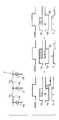
- FIG. 1The figure which shows the structure of a light receiving element (2 capacity
- Diagram showing differential output sequence Diagram showing the concept of this disclosureThe figure which shows the sequence which implement
- segmentation subexposureThe figure which shows the sequence explaining the principle which acquires a ranging value from the subexposure of 2 divisions
- FIG. 11is a diagram showing a sequence for realizing four-phase distance measurement exposure by sub-exposure divided into four (part 1).
- FIG. 2is a diagram showing a sequence for realizing 4-phase distance measurement exposure by sub-exposure of 4 divisions (part 2)
- FIG. 3shows a sequence for realizing 4-phase distance measurement exposure by sub-exposure of 4 divisions (No.
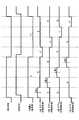
- FIG. 3Part of a distance measurement value acquisition circuit (part 1) The figure which shows the timing chart which shows the output of an output signal (the 1) Part of a distance measurement value acquisition circuit (part 2) Timing chart showing output of output signal (Part 2) The figure which shows the timing chart which performs rolling reset and rolling reading (the 1) The figure which shows the timing chart which performs rolling reset and rolling reading (the 2) The figure which shows the timing chart which performs global reset and rolling reading (the 1) A diagram showing a timing chart for performing a global reset and a rolling read (part 2) FIG. 3 is a timing chart for performing global reset and rolling readout (part 3). FIG. 6 is a timing chart for performing control for optimizing the amplitude of each pixel of output accumulated for a long time (part 1). FIG.
- FIG. 2is a timing chart for performing control for optimizing the amplitude of each pixel of the output accumulated for a long time (part 2)
- FIG. 3is a timing chart for performing control for optimizing the amplitude of each pixel of a long-time accumulation output (part 3);
- FIG. 3shows a part of a distance measurement value acquisition circuit (part 3) Diagram showing wiring (part 1)
- FIG. 4is a diagram showing a part of a distance measurement value acquisition circuit (No. 4) Diagram showing wiring (part 2) The figure which shows the structure of the light receiving element (2 capacity
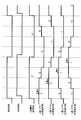
- FIG. 1shows an arrangement form of pixels (No. 1) FIG.
- FIG. 2is a diagram showing an arrangement form of pixels (No. 2) The figure which shows the aspect which switches exposure time for every pixel
- FIG. 3is a diagram showing the arrangement of pixels (No. 3)
- FIG. 4is a diagram showing an arrangement form of pixels (No. 4).
- the functional block diagramwhich is the 3rd Embodiment of this indication, and shows the structure of a differential output
- the sequence of the differential output configurationis shown (Part 1).
- the sequence of the differential output configurationis shown (Part 2).
- the figure which shows the timing chart which performs multiple exposure in the structure of a differential output(the 2) The sequence of the structure of differential output is shown (part 3) The figure which shows the timing chart which performs multiple exposure in the structure of a differential output (the 3) The figure which shows the structure of the light receiving element (1 capacity
- the present disclosureis applied to, for example, an in-vehicle optical flight rangefinder that can be mounted on a vehicle
- the object for calculating the distance from the own deviceis, for example, a person, a vehicle, a wall, or the like.
- the light receiving element 101has a PD (Photodiode) 102, two modulation switches 103a and 103b, and two storage capacitors 104a and 104b.
- a group of pixels Arepeats driving 1000 times to perform long-time exposure
- a group of pixels Brepeats driving 100 times to perform short-time exposure.
- the dynamic rangeis extended by 20 dB.
- the method according to the reference exampleis based on the premise that the adjacent pixels A and B receive the same reflected light. Therefore, it is difficult to design a lens for collecting light on the light receiving element. When this lens design cannot satisfy the above-mentioned preconditions, a fixed pattern depending on the pixel arrangement is generated. Further, in a configuration in which the group of pixels A and the group of pixels B are arranged (coexist) in the same row without being divided for each row, there is a risk that the wiring becomes complicated.
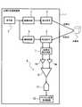
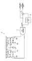
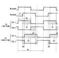
- the optical flight type distance measuring device 1includes a signal source 2, a drive circuit 3 (drive unit), a light emitting element 4, a control circuit 5 (control unit), , A light receiving element 6, a CM (common mode) component removal circuit 7, and a distance measurement value acquisition circuit 8 (a distance measurement value acquisition unit).
- the distance measurement value acquisition circuit 8includes buffers 9 a and 9 b, a difference detection circuit 10, an AD conversion circuit 11, and a digital signal processing circuit 12.
- the signal source 2establishes synchronization between the light emitting element 4 and the light receiving element 6 by outputting a drive signal to the drive circuit 3 and the control circuit 5, and synchronizes with the modulated light emitted from the light emitting element 4.
- the exposure of the light receiving element 6is controlled.
- the drive signal output from the signal source 2may be a rectangular pulse (usually several to several tens of MHz) for driving the light emitting element 4 and the light receiving element 6, or may be only a synchronization pulse.
- the light emitting element 4is, for example, an LD (Laser Diode) or LED (Light Emitting Diode) that emits infrared light as modulated light.
- the light receiving element 6is an image sensor using, for example, a process of CMOS (Complementary Metal Oxide Semiconductor) or CCD (Charge Coupled Device).
- the light receiving element 6includes a PD (Photodiode) 13, two modulation switches 14a and 14b, and two storage capacitors 15a and 15b.
- the two modulation switches 14a and 14bare, for example, MOS type devices such as MOS transistors and transfer gates, CCD structure devices, and the like.
- the two storage capacitors 15a and 15bare, for example, capacitive elements such as MOS, CCD, and MIM (Metal Insulator Metal), wiring, and parasitic capacitance of a PN junction.
- the light receiving element 6drives the modulation switches 14a and 14b with control signals (gate signals) TG1 and TG2, distributes charges generated by the received incident light to the storage capacitors 15a and 15b, and indicates a charge amount of the allocated charges. Is output to the CM component removal circuit 7. Since the control signals TG1 and TG2 are signals synchronized with the modulated light, the amount of charge distributed to the storage capacitors 15a and 15b changes according to the distance from the device to the object. In FIG. 2, two storage capacitors 15a and 15b are illustrated, but three or more storage capacitors may be provided.
- the CM component removal circuit 7avoids saturation of pixels due to charges generated due to background light when there is background light at a level that cannot be ignored with respect to the emitted modulated light. .
- various techniqueshave been disclosed in the prior literature. For example, it is disclosed in US Pat. No. 6,919,549 B2, German Patent No. 102005056774A1, European 1622,200A1, etc.
- the difference detection circuit 10detects a difference between signals input from the CM component removal circuit 7 via the buffers 9a and 9b, and outputs a signal corresponding to the detected difference to the AD conversion circuit 11.
- the buffers 9a and 9bare realized by, for example, a source follower circuit because of their simplicity.
- the difference detection circuit 10is realized by, for example, a differential amplifier.
- the AD conversion circuit 11converts the signal input from the difference detection circuit 10 from an analog signal to a digital signal and outputs the signal to the digital signal processing circuit 12.
- the digital signal processing circuit 12performs digital signal processing on the signal input from the AD conversion circuit 11 and calculates the distance from the device to the target object based on the charge amount distributed to the storage capacitors 15a and 15b. Is obtained (ranging).
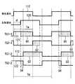
- FIG. 3shows a sequence (modulation cycle: Tm, exposure period: Tw) in the case where four-phase ranging is performed with the duty of the light emission waveform set to 50% (the light receiving element 6 is driven with four phases).
- the waveform of the modulated light emitted from the light emitting element 4(light emission waveform 110) is modulated with a rectangular wave synchronized with the control signals TG1 and TG2.
- FIG. 3illustrates the case of modulation with a rectangular wave, it may be modulated with a waveform such as a sine wave, a triangular wave, or a pseudo-random sequence.
- the waveform of the reflected light reflected from the object (reflected waveform 120) with respect to the modulated lighthas a time difference with respect to the light emission waveform 110, so that the waveform is delayed by the phase difference ⁇ with respect to the light emission waveform 110.
- the control signals TG1 and TG2are driven by rectangular waves having different phases by 180 degrees.
- the digital signal processing circuit 12repeats the sequence driven by the control signals TG1-1 and TG2-1 (drive waveforms 111 and 121) for several tens to hundreds of thousands of cycles, and then generates information on the generated charges Q1 and Q2. (Voltage value after charge-voltage conversion) is acquired.
- the digital signal processing circuit 12repeats the sequence driven by the control signals TG1-2 and TG2-2 (drive waveforms 112 and 122) in the same manner for several tens to hundreds of thousands of times, and then generates the generated charge Q3. , Q4 information is acquired. Then, the digital signal processing circuit 12 calculates the estimated value ⁇ of the phase difference ⁇ from the acquired Q1 to Q4 by using the discrete Fourier transform (DFT: Discrete Fourier Transform) by the following arithmetic expression (1).
- DFTdiscrete Fourier transform
- phase difference ⁇tan-1 [(Q1-Q3) / (Q2-Q4)] (1)
- the calculation formula (1)is a calculation formula for the phase difference based on the above four samplings, but the estimated value ⁇ of the phase difference ⁇ (hereinafter referred to as the phase difference ⁇ ) for the general N phase is expressed by the following calculation formula (2 ).
- FIG. 4shows a differential output sequence.
- the difference detection circuit 10repeats the combination of the control signals TG1 and TG2, for example, the control signals TG1-1 (driving waveform 111) and TG2-1 (driving waveform 121) several tens to several hundred thousand times, to obtain a digital value D1 (201). Is generated.
- the difference detection circuit 10generates a digital value D2 (202) from the control signals TG1-2 (drive waveform 112) and TG2-2 (drive waveform 122), and controls the signal TG1-3 (drive waveform 113).
- the difference detection circuit 10outputs the digital values D1 to D4 as values obtained by removing the DC component.
- “1”is assigned when the control signal TG1 is “H” and TG2 is “L”, the control signal TG1 is “L” and TG2 is “H”.
- "-1"is assigned and described. That is, the state of the control signals TG1 and TG2 is uniquely determined depending on whether the value of the waveform of Dx is “1” or “ ⁇ 1”.
- the AD conversion circuit 11Since Dx is a signal indicating the difference between the two storage capacitors 15a and 15b as described above, the AD conversion circuit 11 outputs a signal on which an operation corresponding to the numerator or denominator of the above-described arithmetic expression (1) is performed. Output.
- phase type optical flight range finder 1when such a phase type optical flight range finder 1 is used on a vehicle or the like, it is required to expand the dynamic range.
- a method for extending the dynamic range according to the present disclosurewill be described.
- FIG. 5shows the concept of the present disclosure.
- the present disclosuredivides the basic exposure period corresponding to the long-time accumulation period of the reference example described above into a plurality of sub-exposure periods, thereby obtaining a short-range exposure distance value and the exposure (long) of the reference example. A distance measurement value of long exposure equivalent to (time exposure) is acquired.
- FIG. 6shows a sequence for realizing the four-phase ranging exposure of the reference example by the sub-exposure divided into two
- FIG. 7shows a timing chart thereof.
- a distance value for short-time exposurecan be acquired (updated at high speed) from the amount of charge accumulated within one period (within one period) of the plurality of sub-exposure periods divided in this way. . Further, it is possible to obtain a distance measurement value for long-time exposure by integrating the amount of charge accumulated in a plurality of rounds. That is, by devising the timing to read out the electric charge (output value) accumulated in one pixel (the same pixel), both the short-range exposure distance value and the long-exposure distance measurement value from one pixel.
- the dynamic rangecan be expanded.
- FIG. 8shows the principle of obtaining a distance measurement value from two sub-exposures.
- FIG. 6shows a comparison between the sequence of FIG. 6 in which the exposure of the four-phase ranging in the reference example is realized by the sub-exposure divided into two and the sequence in the case of performing the four-capacity / 4-phase ranging in another reference example.
- Sub-exposure 1corresponds to an exposure of 0 to 180 degrees in a sequence for performing 4 volume / 4 phase ranging
- sub-exposure 2corresponds to 90 to 270 degrees in a sequence for performing 4 capacitance / 4 phase ranging.
- Thiscorresponds to the numerator and denominator of the following arithmetic expression (3) for calculating the phase difference ⁇ of the four-phase ranging.
- FIG. 8shows the case where the sub-exposure is based on four phases, but the same idea holds for a general N (N is a natural number) phase.
- Nis a natural number
- an arithmetic expression of the discrete Fourier transformis given by the following arithmetic expression (4).
- the primary componentis mainly used in the phase type flight type distance measurement, and the calculation formula (4) is given by the following calculation formula (5).
- the sub-exposure driving waveformso that the divided sub-exposure becomes a j ⁇ a N / 2 + j .
- hierarchical rangingbased on the principle of the present disclosure is established for an arbitrary division method To do.
- the drive waveformis determined so that the relationship between the 1 and -1 waveforms is 180 degrees in phase difference.
- the methods for realizing “0”include the following first to third methods, for example.
- a period in which the modulation switches 14a and 14b are simultaneously turned onthat is, a period in which both TG1 and TG2 are “H” is provided to realize “0”.
- the charges generated in the PD 13 during the period when both TG1 and TG2 are “H”are divided into Qa and Qb and accumulated in the storage capacitors 15a and 15b, and Qa and Qb have the same value. Therefore, this component is canceled by the CM component removal circuit 7 and the difference detection circuit 10, and as a result, the AD conversion circuit 11 outputs “0”.
- a modulation switch 14c different from the modulation switches 14a and 14bis provided, the period in which the modulation switches 14a and 14b are turned off simultaneously and the other modulation switch 14c is turned on, that is, “0” is realized by providing a period in which both TG1 and TG2 are “L” and TG3 is “H”.
- the charges generated in the PD 13 during the period when both TG1 and TG2 are “L” and TG3 is “H”are discarded to a fixed potential (for example, VDD).
- one of Qa and Qbis discarded and “0” is realized by integrating two samples. That is, the period for discarding the charges accumulated during the period when TG2 is “H” and the period for discarding the charges accumulated during the period when TG1 is “H” are integrated.
- the first method described aboveit is necessary to provide a period in which both TG1 and TG2 are “H”.
- the second methodit is necessary to provide a period in which both TG1 and TG2 are “L”.
- the method 3does not need to provide such a period, and it is sufficient to perform control to invert TG1 and TG2, and there is an advantage that simple control is sufficient.
- FIG. 12shows a sequence for realizing 4-phase ranging exposure by sub-exposure divided into 4 parts.
- starting sub-exposure with a waveform having a duty of 12.5%is equivalent to 8-capacity / 8-phase ranging.
- FIG. 13shows another sequence for realizing 4-phase distance measurement exposure by sub-exposure divided into 4 parts.
- the sub-exposureis started with a waveform having a duty of 37.5%.
- the exposure timeneeds to be quadrupled, but in FIG. By making the signal integration time in the sub-exposure longer than the sequence shown in FIG.
- FIG. 14shows still another sequence for realizing the 4-phase distance measurement exposure by the sub-exposure divided into four.
- the sub-exposureis activated with a waveform having a duty of 50%.
- FIG. 12 and FIG. 13it is necessary to perform control for inserting “0”.
- FIG. 14the SNR obtained at the same exposure time is inferior to the sequence shown in FIG. It can be unnecessary.
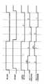
- FIG. 15shows a circuit diagram in which a part of the distance measurement value acquisition circuit 8 that is a subsequent stage of the light receiving element 6 is configured using an analog memory
- FIG. 16shows a timing chart of its operation.
- the distance measurement value acquisition circuit 8includes a light receiving element 6 (PD13, modulation switches 14a and 14b, storage capacitors 15a and 15b), buffers 9a and 9b, reset switching elements 21a and 21b, and selector switching elements 22a and 22b. Is connected.
- These buffers 9a and 9b, switching elements 21a and 21b, and switching elements 22a and 22bare configured by, for example, field effect transistors (FETs).
- FETsfield effect transistors
- the analog differential signal processing circuit 23reads the charge amount differentially from the light receiving element 6 and outputs an output signal to the analog memory 24 and the difference calculation circuit 25.
- the analog memory 24holds the output value of the input output signal.
- the analog memory 24outputs the output signal including the held output value.
- the difference calculation circuit 25calculates and outputs the difference by subtracting the output value of the output signal input from the analog memory 24 from the output value of the output signal input from the analog differential signal processing circuit 23.
- the distance measurement value acquisition circuit 8outputs an output signal directly output from the analog differential signal processing circuit 23 as a distance measurement value for long exposure, and outputs an output signal output from the difference calculation circuit 25 for short exposure measurement. Output as distance value.
- the increase in circuit area and the influence of noiseare problems as compared with the configuration in which the difference is calculated by the digital circuit described later, but the influence of the quantization error can be suppressed. .
- FIG. 17shows a circuit diagram in which a part of the distance measurement value acquisition circuit 8 that is a subsequent stage of the light receiving element 6 is configured using a digital memory
- FIG. 18shows a timing chart of its operation.
- the AD conversion circuit 11reads the charge amount from the light receiving element 6 differentially and performs AD conversion, and outputs an output signal to the digital memory 31 and the difference calculation circuit 32.
- the digital memory 31holds the output value of the input output signal, and when the next output signal is input, the digital memory 31 converts the output signal including the held output value into a difference calculation circuit. 32.
- the difference calculation circuit 32subtracts the output value of the output signal input from the digital memory 31 from the output value of the output signal input from the AD conversion circuit 11 and calculates and outputs the difference. That is, the distance value acquisition circuit 8 outputs the output signal directly output from the AD conversion circuit 11 as a distance value for long exposure, and the output signal output from the difference calculation circuit 32 as a distance value for short exposure. Output.
- the influence of the quantization errorbecomes a problem as compared with the configuration in which the difference is calculated by the analog circuit described above, but the influence of the circuit area and noise can be suppressed.
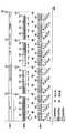
- FIG. 19shows a timing chart for performing rolling reset and rolling reading.
- the long-time accumulation timedoes not need to be a multiple of the number of read rows.
- the analog differential signal processing circuit 23 and the analog memory 24 shown in FIG. 15, the AD conversion circuit 11 and the digital memory shown in FIG. 31may be provided for each column.
- FIG. 20shows another timing chart for performing rolling reset and rolling reading.
- the sub-exposure sequenceis stopped before and after the exposure time of the rolling shutter.
- the exposureis the same globally. It may be implemented with a driving waveform, and only reading may be realized by rolling reset.
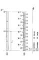
- FIG. 21shows a timing chart for performing global reset and rolling readout. Since the global reset requires that all pixel values be held in the memory, the circuit scale increases, but it is possible to suppress problems (so-called focal plane distortion) associated with the inability to guarantee the simultaneity of exposure for each column. it can.
- FIG. 22shows another timing chart for performing global reset and rolling readout.
- a global shutter for long-time storage and a rolling shutter for short-time storagean output with almost no focal plane distortion can be obtained on the long-time storage side.
- the analog differential signal processing circuit 23 and the analog memory 24 shown in FIG. 15 and the AD conversion circuit 11 and the digital memory 31 shown in FIG. 17may be provided for each column.
- FIG. 23shows still another timing chart for performing global reset and rolling readout.
- the frame rate on the sub-exposure sideis regulated by the pixel readout time
- the frame ratecan be increased by thinning out the sub-exposure rolling shutter. If the distance from the device to the target is close or the target is a highly reflective object, there is a high possibility that the measurement will be performed across multiple lines. .
- FIG. 24is a timing chart for optimizing the amplitude for each pixel of the output accumulated for a long time.
- the exposurewas further repeated. Since the amplitude was sufficient when reading was performed in the second round, the exposure was stopped in the second round. Since the exposure control line is common to the rows, the average value, maximum value, or minimum value of the corresponding row is used to determine whether the amplitude is sufficient.
- FIG. 25shows another timing chart for optimizing the amplitude for each pixel of the output accumulated for a long time.
- FIG. 26shows still another timing chart for optimizing the amplitude for each pixel of the output accumulated for a long time.
- FIG. 25 described aboveis a case where the rolling reset is applied, but also when the global reset is applied, a reset may be inserted for each pixel with respect to a pixel having a high sub-exposure output value.
- FIG. 27shows a circuit diagram that enables adaptive reset for each pixel
- FIG. 28shows the wiring thereof.
- the distance measurement value acquisition circuit 8includes, in addition to the buffers 9a and 9b, the reset switching elements 21a and 21b, and the selector switching elements 22a and 22b, the column reset switching elements 23a and 23b.
- the selector switching elements 24a and 24bare connected.
- FIG. 29shows another circuit diagram in which each pixel can be adaptively reset
- FIG. 30shows its wiring. Since all the CRST lines are simultaneously set to “H” in the configuration of FIG. 27, the reset for each row can be performed, so that the RST lines become redundant. That is, in FIG. 29, the RST line in the configuration of FIG. 27 is omitted.
- the basic exposure period corresponding to the long-time accumulation of the reference exampleis divided into a plurality of sub-exposure periods, and the plurality of sub-exposure periods are accumulated within the sub-exposure period within one period. Hold the charged charge without resetting it. Then, a distance measurement value for short-time exposure is obtained from the charge amount of the charge accumulated in one cycle period, and the charge amount of charge accumulated in a plurality of one-cycle periods is integrated to obtain a long exposure time. By acquiring the distance measurement value, both the long-range exposure distance measurement value and the short-time exposure distance measurement value are acquired from one pixel (the same pixel).
- the dynamic rangecan be extended without being restricted by the reflected light reception state, the light receiving optical system design, and the pixel arrangement. This is particularly suitable in the case of a vehicle or the like in which at least one of the own apparatus and the object moves. (Second Embodiment) Next, the flight type distance measuring device according to the second embodiment will be described below.
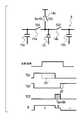
- the light receiving element 1101has a PD (Photodiode) 1102, two modulation switches 1103a and 1103b, and one storage capacitor 1104, and performs four-phase ranging.
- PDPhotodiode
- the casewill be described as an example.
- the pixel group of the pixel Arepeats driving for 1000 times to perform long-time exposure
- the pixel group of the pixel Brepeats driving for 100 times to perform short-time exposure.
- the dynamic rangecan be extended by 20 dB.
- the frame ratecan be increased compared to the case where multiple exposure is performed in series. Yes.
- the distanceis calculated after reading out the values of 0 degree, 90 degrees, 180 degrees, and 270 degrees, so the frame rate of the short exposure Will be governed by the long exposure time.
- the method according to the comparative examplehas a limit in increasing the frame rate of the short-time exposure.
- the optical flight rangefinder of the second embodimentthat can appropriately expand the dynamic range and can appropriately increase the frame rate of short-time exposure is shown in FIGS. 45 will be described in detail below.
- the second embodimenthas a single-ended output configuration.
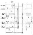
- the optical flight type distance measuring device 201includes a signal source 202, a drive circuit 203 (drive unit), a light emitting element 204, a control circuit 205 (control unit), a light receiving element 206, and a distance measurement value acquisition circuit 207 (measurement value).
- the distance measurement value acquisition circuit 207includes a buffer 208, an AD conversion circuit 209, and a digital signal processing circuit 210.
- the signal source 202establishes synchronization between the light emitting element 204 and the light receiving element 206 by outputting a driving signal to the driving circuit 203 and the control circuit 205, and synchronizes with the modulated light emitted from the light emitting element 204.
- the exposure of the light receiving element 206is controlled.
- the drive signal output from the signal source 202may be a rectangular pulse (usually several to several tens of MHz) for driving the light emitting element 204 and the light receiving element 206, or may be only a synchronization pulse.
- the light emitting element 204is, for example, an LD (Laser Diode) or an LED (Light Emitting Diode) that emits infrared light as modulated light.
- the light receiving element 206is an image sensor using a process of CMOS (Complementary Metal Oxide Semiconductor) or CCD (Charge Coupled Device), for example.
- the light receiving element 206includes a PD (Photodiode) 211, two modulation switches 212a and 212b, and one storage capacitor 213.
- the two modulation switches 212a and 212bare, for example, MOS type devices such as MOS transistors and transfer gates, CCD structure devices, and the like.
- the storage capacitor 213is, for example, a capacitive element such as a MOS, CCD, or MIM (MetalMetaInsulator Metal), a wiring, a parasitic capacitance of a PN junction, or the like.
- the light receiving element 206drives the modulation switches 212a and 212b with a control signal (gate signal) TG1, accumulates charges generated by the received incident light in the storage capacitor 213, and obtains a distance value obtained from the signal indicating the charge amount of the charges. Output to the circuit 207. Since the control signal TG1 is a signal synchronized with the modulated light, the amount of charge accumulated in the storage capacitor 213 changes according to the distance from the device to the target.
- the buffer 208is realized by, for example, a source follower circuit because of its simplicity.
- the AD conversion circuit 209converts the signal input from the buffer 208 from an analog signal to a digital signal and outputs the signal to the digital signal processing circuit 210.
- the digital signal processing circuit 210performs digital signal processing on the signal input from the AD conversion circuit 209, calculates the distance from its own device to the object from the charge amount stored in the storage capacitor 213, and obtains a distance measurement value. (Measure distance).
- FIG. 36shows a sequence (modulation cycle: Tm, exposure period: Tw) in the case where four-phase ranging is performed with the duty of the light emission waveform being 50% (the light receiving element 206 is driven with four phases).
- the waveform of the modulated light emitted from the light emitting element 204(light emission waveform 2110) is modulated with a rectangular wave synchronized with the control signal TG1.
- FIG. 36illustrates the case of modulation with a rectangular wave, but modulation may be performed with a waveform such as a sine wave, a triangular wave, or a pseudo-random sequence.
- the waveform of the reflected light (reflected waveform 2120) reflected by the object with the modulated lighthas a time difference with respect to the light emission waveform 2110, and therefore is a waveform delayed by the phase difference ⁇ with respect to the light emission waveform 2110.
- the control signal TG1is driven by rectangular waves whose phases are different by 90 degrees.
- the digital signal processing circuit 210repeats the sequence driven by the control signals TG1-1 and TG1-2 (drive waveforms 2111, 2112) for several tens to several hundreds of thousands of cycles, and then generates information on the generated charges Q1, Q2. (Voltage value after charge-voltage conversion) is acquired.
- the digital signal processing circuit 210repeats the sequence driven by the control signals TG1-3, TG1-4 (drive waveforms 2113, 2114) in the same manner for several tens to hundreds of thousands of times, and then generates the generated charge Q3. , Q4 information is acquired. Then, the digital signal processing circuit 210 calculates the phase difference ⁇ from the acquired Q1 to Q4 using the discrete Fourier transform (DFT: Discrete Fourier Transform) according to the arithmetic expression (1) described in the first embodiment.
- DFTdiscrete Fourier transform
- phase-type optical flight range finder 201when such a phase-type optical flight range finder 201 is used on a vehicle or the like, it is required to expand the dynamic range and to improve the frame rate for short-time exposure.
- a method for increasing the frame rate of short-time exposure while extending the dynamic range according to the present disclosurewill be described.
- FIG. 37is a timing chart of multiple exposure in the single-ended output configuration of the present disclosure.
- the control circuit 205converts the plurality of pixels in the plane into the pixel group of the pixel A and the pixel group of the pixel B. The points are divided into the same.
- the control circuit 205accumulates and reads out charges in a plurality of phases instead of a single phase in the pixel group of the pixel B within a period in which the pixel group of the pixel A is exposed for a long time. Thus, a plurality of short-time exposures are performed.
- the number of times the distance measurement value is acquiredis larger than that of the multiple exposure of the comparative example when compared in the same period, the distance measurement value can be updated frequently, and the frame rate is increased. be able to.
- the drivingis performed according to the timing chart of FIG.
- the frame ratecan be four times that of the above.
- the frame ratecan be increased for objects that are close or highly reflective. That is, it is particularly suitable in an environment where it is required to frequently calculate the distance (increase the frame rate) in order to avoid a collision with an object (a person, a vehicle, a wall, etc.) such as a vehicle.
- FIG. 38shows another multiple exposure timing chart having a single-ended output configuration.
- the frame rate ratio between the long time exposure and the short time exposureis “4”, but the frame rate ratio is not limited to “4”. That is, the frame rate can be further increased by increasing the number of short-time exposure cycles (the number of repetitions) with respect to the long-time exposure.
- a frame rate 12 times as high as that of the timing chart of FIG. 56can be realized, and a frame rate of 3 times that of the case of driving with the timing chart of FIG. be able to.
- the frame ratecan be lowered by reducing (thinning out) the number of short-time exposure cycles with respect to long-time exposure from the viewpoint of subsequent signal processing.
- FIG. 39shows still another multiple exposure timing chart having a single-end output configuration.
- the distance measurement valueis acquired at least once by the short exposure within the period of each phase of the long exposure, but the distance measurement is performed by the short exposure within the period extending over a plurality of phases of the long exposure. You may acquire a value once.
- the frame ratecan be doubled as compared with the case of driving with the timing chart of FIG.
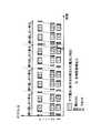
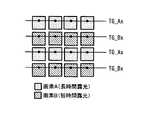
- FIG. 40 and 41show an arrangement form in which a plurality of pixels in a plane are divided into two pixel groups.
- the long exposure pixel group A and the short exposure pixel group Bare divided for each row.
- the wiring of the control lines for driving the modulation switches 12a and 12bcan be made common, and the frame rate for short-time exposure can be increased without greatly changing the existing configuration.
- the long exposure pixel group A and the short exposure pixel group Bare divided into a checkered pattern (check).
- FIG. 42shows a mode in which a long exposure pixel group and a short exposure pixel group are switched over time.
- reflected light reflected by an object having a long distance from the apparatus or having a low reflectanceis received by only one pixel in some cases. Therefore, if the long-exposure pixel group and the short-exposure pixel group are fixed, there is a possibility that an object for which a distance measurement value cannot be obtained will appear.
- the occurrence of the above-described problemcan be avoided in advance by switching the long exposure pixel group and the short exposure pixel group by time (for example, in units of frames).
- the example of FIG. 42is a mode in which the long exposure pixel group and the short exposure pixel group shown in FIG. 40 are switched in the configuration divided for each row, but the long exposure shown in FIG. It is possible to switch similarly in the configuration in which the pixel group and the short-time exposure pixel group are divided into a checkered pattern.
- FIG. 43shows still another multiple exposure timing chart having a single-ended output configuration.
- the in-plane pixelsare divided into two pixel groups, but may be divided into three pixel groups.
- the frame ratethat is four times that of the pixel group of the pixel A that performs long-time exposure can be realized, and the pixel C that performs short-time exposure.
- this pixel groupit is possible to realize a frame rate 12 times that of the pixel group of the pixel A that is exposed for a long time.
- FIG. 44 and 45show an arrangement in which a plurality of pixels in a plane are divided into three pixel groups (one pixel group, first other pixel group, and second other pixel group).
- the pixels Care arranged in all rows, and the pixels A and the pixels B are divided at intervals of one row.
- the number of control lines required per rowbecomes two types in all the rows, and it becomes easy to share them, and the spatial resolution can be increased when an image is composed of only the pixel group of the pixel C.
- the pixels Amay be arranged in all rows and the pixels B and C may be divided at intervals of one row, or the pixels B may be arranged in all rows and the pixels A and C may be arranged.
- the pixels A, B, and Care divided so as to be arranged in all rows.
- the number of control lines required per rowis three types in all rows, making it difficult to share, but an image is configured only by any pixel group of pixel A, pixel B, and pixel C. Even in this case, the spatial resolution can be increased. Even when a plurality of pixels in the plane are divided into three pixel groups in this way, the respective pixel groups may be switched by time.
- the dynamic rangecan be expanded by dividing a plurality of pixels in the plane into a pixel group that performs long-time exposure and a pixel group that performs short-time exposure.
- the light receiving element of the pixel group that performs short exposureis subjected to multiple short exposures within a period in which the light receiving element of the pixel group that performs long exposure acquires a distance measurement value once by one long exposure.
- the frame rate for short-time exposurecan be increased. Thereby, it is possible to appropriately increase the frame rate for short-time exposure while appropriately extending the dynamic range. This is particularly suitable in the case of a vehicle or the like in which at least one of the own apparatus and the object moves.
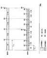
- the optical flight rangefinder 321includes a signal source 322, a drive circuit 323 (drive unit), a light emitting element 324, a control circuit 325 (control unit), a light receiving element 326, and a CM (common mode) component removal circuit. 327 and a distance value acquisition circuit 328 (range value acquisition unit).
- the distance measurement value acquisition circuit 328includes buffers 329a and 329b, a difference detection circuit 330, an AD conversion circuit 331, and a digital signal processing circuit 332.
- the signal source 322, the drive circuit 323, the light emitting element 324, and the control circuit 325are the same as the signal source 202, the drive circuit 203, the light emitting element 204, and the control circuit 205 described in the second embodiment, respectively.
- the light receiving element 326includes 3PD 41, two modulation switches 342a and 342b, and two storage capacitors 343a and 343b.
- the light receiving element 326drives the modulation switches 342a and 342b with the control signals TG1 and TG2, distributes and accumulates the charges generated by the received incident light in the storage capacitors 343a and 343b, and a signal indicating the charge amount of the charge as a CM component Output to the removal circuit 327.
- control signals TG1 and TG2are signals synchronized with the modulated light
- the amount of charges distributed and accumulated in the storage capacitors 343a and 343bchanges according to the distance from the device to the target.
- two storage capacitors 343a and 343bare illustrated, but three or more storage capacitors may be provided.
- the CM component removal circuit 327avoids pixel saturation due to charges generated due to background light when there is background light at a level that cannot be ignored with respect to the modulated light that is emitted. .
- various techniqueshave been disclosed in the prior literature. For example, it is disclosed in US Pat. No. 6,919,549 B2, German Patent No. 102005056774A1, European 1622,200A1, etc.
- the difference detection circuit 330detects a difference between signals input from the CM component removal circuit 327 via the buffers 329a and 329b, and outputs a signal corresponding to the detected difference to the AD conversion circuit 331.
- the difference detection circuit 330is realized by, for example, a differential amplifier.
- the AD conversion circuit 331converts the signal input from the difference detection circuit 330 from an analog signal to a digital signal and outputs the signal to the digital signal processing circuit 332.
- the digital signal processing circuit 332performs digital signal processing on the signal input from the AD conversion circuit 331, and calculates the distance from the own device to the target object from the charge amount of the charge distributed and stored in the storage capacitors 343a and 343b. Acquires a distance measurement value (measures a distance).
- FIG. 48shows a sequence in a case where four-phase ranging is performed with the duty of the light emission waveform being 50% (the light receiving element 326 is driven with four phases).
- the difference detection circuit 330generates a digital value D1 by repeating a combination of control signals TG1 and TG2, for example, control signals TG1-1 (drive waveform 3111) and TG2-1 (drive waveform 3121) several tens to several hundred thousand times. .
- the difference detection circuit 330generates the digital value D2 by repeating the control signals TG1-2 (drive waveform 3112) and TG2-2 (drive waveform 3122) several tens to several hundred thousand times.
- the difference detection circuit 330outputs the digital values D1 and D2 as values obtained by removing the DC component.
- FIG. 49is a timing chart of multiple exposure in the configuration of the operation output of the present disclosure.
- the pixel group of the pixel Athat performs long-time exposure by the pixel group of the pixel B performing six short-time exposures within the period in which the pixel group of the pixel A performs one long-time exposure.
- a frame ratethat is six times that of the group can be realized.
- FIG. 50shows another sequence of the operation output of the present disclosure
- FIG. 51shows a timing chart of multiple exposure corresponding to the sequence.
- the control signals TG1-3drive waveform 3113
- TG2-3drive waveform 3123
- the digital value D3is generated by repeating several hundred thousand times
- the digital value D4is generated by repeating the control signals TG1-4 (drive waveform 3114) and TG2-4 (drive waveform 3124) several tens to several hundred thousand times.
- FIG. 52shows still another sequence of the operation output of the present disclosure
- FIG. 53shows a timing chart of multiple exposure corresponding to the sequence.
- the number of phases for long exposure and the number of phases for short exposureneed not be the same, and may be different.
- long exposureis driven by 6-phase ranging
- short exposureis driven by 4-phase ranging.
- “0”indicating a non-integration period which is a period in which the signal is not integrated is inserted, so Sensitivity is given to harmonics.
- the characteristic that the energy of the higher-order harmonic component increases as the duty becomes shorteris used.
- sensitivity to a predetermined higher-order harmonicis used.
- the digital signal processing circuit 332calculates the distance by linearly combining the fundamental wave component and the higher-order harmonic component, thereby adding the higher-order harmonic component and calculating the distance from only the fundamental wave component. The distance error can be reduced as compared with the case of calculation.
- the applicanthas applied for Japanese Patent Application No. 2014-226069 regarding a technique for giving sensitivity to such high-order harmonics.
- the third embodimentnot only the configuration of the single-end output but also the configuration of the differential output can obtain the same effects as those of the second embodiment described above, and the dynamic range. It is possible to appropriately increase the frame rate for short-time exposure.
- the third embodimentis not limited to the configuration in which the pixel groups are divided into two pixel groups, and may be configured to be divided into three pixel groups as in the second embodiment described above. You can switch with.
- the flight type distance measuring device of the present disclosuremay be applied to uses other than in-vehicle use.
- the configuration of dividing into two pixel groups or three pixel groupsis illustrated, but a configuration of dividing into four or more pixel groups having different exposure periods may be used. Even when the pixel group is divided into four or more pixel groups, each pixel group may be switched by time.
- phase numbers of long exposure and short exposure when divided into two pixel groupsand long exposure and medium time exposure when divided into three pixel groups
- Any combination of phase numbers for short-time exposuremay be used.
- any combination of the respective phase numbersmay be used.
Landscapes
- Engineering & Computer Science (AREA)
- Physics & Mathematics (AREA)
- Computer Networks & Wireless Communication (AREA)
- General Physics & Mathematics (AREA)
- Radar, Positioning & Navigation (AREA)
- Remote Sensing (AREA)
- Electromagnetism (AREA)
- Multimedia (AREA)
- Signal Processing (AREA)
- Optical Radar Systems And Details Thereof (AREA)
- Measurement Of Optical Distance (AREA)
Abstract
Description
Translated fromJapanese本出願は、当該開示内容が参照によって本出願に組み込まれた、2014年11月14日に出願された日本特許出願2014-231630号および2014年11月21日に出願された日本特許出願2014-236484号を基にしている。This application includes Japanese Patent Application No. 2014-231630 filed on November 14, 2014 and Japanese Patent Application 2014-2014 filed on November 21, 2014, the disclosures of which are incorporated herein by reference. Based on 236484.
本開示は、繰り返し周期を持つパターンで変調された変調光を空間に発光し、変調光が対象物で反射した反射光を含む入射光に応じた電荷を用いて自装置から対象物までの距離を計算する光飛行型測距装置に関する。This disclosure emits modulated light modulated in a pattern having a repetitive period in a space, and uses a charge corresponding to incident light including reflected light that is reflected by the object to be reflected from the device itself to the object. The present invention relates to an optical flight type distance measuring device that calculates
自装置から対象物までの距離を非接触で計算する測距装置として、光飛行(TOF:Time of Flight)型測距装置が供されている。光飛行型測距装置は、繰り返し周期を持つパターンで変調された変調光(測距光)を空間に発光し、変調光が対象物で反射した反射光を含む入射光を受光する。そして、光飛行型測距装置は、受光した入射光に応じた電荷を複数の変調スイッチにより振り分けて複数の蓄積容量に蓄積し、サンプリングした値を用いて自装置から対象物までの距離を計算する(例えば特許文献1~4参照)。As a distance measuring device that calculates the distance from its own device to an object without contact, a time-of-flight (TOF) distance measuring device is provided. The optical flight-type distance measuring device emits modulated light (ranging light) modulated in a pattern having a repetition period into a space, and receives incident light including reflected light reflected by the object. The optical flight-type distance measuring device distributes charges according to the received incident light by a plurality of modulation switches and accumulates them in a plurality of storage capacitors, and calculates the distance from the own device to the object using the sampled values. (For example, see
光飛行型測距装置においては、自装置から対象物までの距離が近かったり対象物が高反射率の物体であったりすると、強い強度の反射光を受光する。一方、自装置から対象物までの距離が遠かったり対象物が低反射率の物体であったりすると、弱い強度の反射光しか受光しない。そのため、光飛行型測距装置においては、大きなダイナミックレンジ(例えば80dB以上)が要求される。特に車載等の場合には、自装置及び対象物(人、車両、壁等)のうち少なくとも何れかが移動している状況で、自装置から対象物までの距離が近ければ、対象物への衝突を回避するために距離を頻繁に計算する(フレームレートを高める)ことが要求される。即ち、大きなダイナミックレンジと高いフレームレートとを両立させる必要がある。In the optical flight type distance measuring device, when the distance from the own device to the object is short or the object is an object having a high reflectivity, the reflected light with strong intensity is received. On the other hand, if the distance from the device to the object is long or the object is an object having a low reflectivity, only reflected light having a weak intensity is received. Therefore, a large dynamic range (for example, 80 dB or more) is required in the optical flight type distance measuring device. In particular, in the case of in-vehicle equipment, etc., if at least one of the device itself and the object (person, vehicle, wall, etc.) is moving and the distance from the device to the object is short, It is required to calculate the distance frequently (increase the frame rate) to avoid collisions. That is, it is necessary to achieve both a large dynamic range and a high frame rate.
通常の画素では80dB以上のダイナミックレンジを実現することは難しく、多重露光(多数回の露光)を行う必要がある。ところが、多重露光をシリーズで行うと、露光時間が長くなってしまい、動きのある対象物に対する追従性が劣化する問題が発生する。この点に関し、面内で複数の画素をグループ分けし、グループ毎に露光時間を変える方法が開示されている(例えば非特許文献1、2参照)。It is difficult to achieve a dynamic range of 80 dB or more with ordinary pixels, and multiple exposure (multiple exposures) must be performed. However, when multiple exposure is performed in series, the exposure time becomes long, and a problem arises in that the followability to a moving object is deteriorated. In this regard, a method has been disclosed in which a plurality of pixels are grouped in a plane and the exposure time is changed for each group (for example, see Non-Patent
本開示の第1の目的は、反射光の受光状況や受光光学系の設計や画素の配置の制約を受けることなく、ダイナミックレンジを適切に拡張することができる光飛行型測距装置を提供することにある。本開示の第2の目的は、ダイナミックレンジを適切に拡張することができつつ、短時間露光のフレームレートを適切に高めることができる光飛行型測距装置を提供することにある。A first object of the present disclosure is to provide an optical flight-type distance measuring device capable of appropriately extending a dynamic range without being restricted by a reflected light reception state, a light receiving optical system design, and pixel arrangement. There is. A second object of the present disclosure is to provide an optical flight type distance measuring device capable of appropriately increasing the frame rate of short-time exposure while appropriately extending the dynamic range.
本開示の第1の態様では、発光素子は、繰り返し周期を持つパターンで変調された変調光を空間に発光する。駆動部は、発光素子を駆動する。受光素子は、変調光が対象物で反射した反射光を含む入射光に応じた電荷を複数の変調スイッチにより振り分けて複数の蓄積容量に蓄積する。制御部は、複数の変調スイッチの駆動を制御する。測距値取得部は、受光素子によりサンプリングされた値を用いて自装置から対象物までの距離を計算して測距値を取得する。In the first aspect of the present disclosure, the light emitting element emits modulated light modulated in a pattern having a repetition cycle in space. The driving unit drives the light emitting element. The light receiving element distributes charges corresponding to incident light including reflected light, which is reflected from the object by the modulated light, by a plurality of modulation switches and accumulates the charges in a plurality of storage capacitors. The control unit controls driving of the plurality of modulation switches. The distance measurement value acquisition unit calculates the distance from the own device to the object using the value sampled by the light receiving element, and acquires the distance measurement value.
制御部は、基本露光期間を複数のサブ露光期間に分割するように複数の変調スイッチの駆動を制御し、複数のサブ露光期間が1巡する1巡期間内ではサブ露光期間内に蓄積された電荷をリセットせずに保持する。測距値取得部は、1巡期間内に蓄積された電荷の電荷量から短時間露光の測距値を取得すると共に、複数回の1巡期間内に蓄積された電荷の電荷量を積算して長時間露光の測距値を取得する。The control unit controls driving of the plurality of modulation switches so as to divide the basic exposure period into a plurality of sub-exposure periods, and the plurality of sub-exposure periods are accumulated in the sub-exposure period within one round period. Hold the charge without resetting it. The distance measurement value acquisition unit acquires the distance measurement value of short-time exposure from the charge amount accumulated during one round period, and integrates the charge amount accumulated during a plurality of round periods. To obtain the distance measurement value for long exposure.
第1の態様によれば、複数の画素を長時間露光のグループと短時間露光のグループとにグループ分けてそれぞれ長時間露光の測距値と短時間露光の測距値とを取得する方法とは異なり、基本露光期間を複数のサブ露光期間に分割することで、1つの画素(同じ画素)から長時間露光の測距値と短時間露光の測距値との両方を取得するようにした。これにより、反射光の受光状況や受光光学系の設計や画素の配置の制約を受けることなく、ダイナミックレンジを拡張することができる。特に自装置及び対象物のうち少なくとも何れかが移動する車載等の場合に好適となる。According to the first aspect, a method of grouping a plurality of pixels into a long exposure group and a short exposure group to obtain a long exposure distance value and a short exposure distance value, respectively. In contrast, by dividing the basic exposure period into multiple sub-exposure periods, both long-range and short-range exposure values are obtained from a single pixel (the same pixel). . As a result, the dynamic range can be extended without being restricted by the reflected light reception state, the light receiving optical system design, and the pixel arrangement. This is particularly suitable in the case of a vehicle or the like in which at least one of the own apparatus and the object moves.
本開示の第2の態様では、発光素子は、繰り返し周期を持つパターンで変調された変調光を空間に発光する。駆動部は、発光素子を駆動する。複数の受光素子は、それぞれが面内の画素を構成し、変調光が対象物で反射した反射光を含む入射光を受光する。制御部は、複数の受光素子における電荷の蓄積と複数の受光素子からの電荷の読み出しを制御する。測距値取得部は、複数の受光素子から制御部により読み出された電荷を用いて自装置から対象物までの距離を計算して測距値を取得する。この場合、制御部は、複数の受光素子を幾つかの画素グループに区分し、一の画素グループに属する受光素子が1回の長時間露光を行うことで測距値取得部により測距値が1回取得される期間内に、他の画素グループに属する受光素子が複数回の短時間露光を行うことで測距値取得部により測距値が複数回取得されるように複数の受光素子の駆動を制御する。In the second aspect of the present disclosure, the light emitting element emits modulated light modulated in a pattern having a repetition cycle in space. The driving unit drives the light emitting element. Each of the plurality of light receiving elements constitutes an in-plane pixel and receives incident light including reflected light in which modulated light is reflected by an object. The control unit controls charge accumulation in the plurality of light receiving elements and reading of the charge from the plurality of light receiving elements. The distance measurement value acquisition unit calculates the distance from the own device to the target object using the charges read from the plurality of light receiving elements by the control unit, and acquires the distance measurement value. In this case, the control unit divides the plurality of light receiving elements into several pixel groups, and the distance measurement value is obtained by the distance measurement value acquiring unit when the light receiving elements belonging to one pixel group perform one long exposure. Within a period acquired once, the light receiving elements belonging to other pixel groups perform a plurality of short-time exposures so that the distance measurement value is acquired a plurality of times by the distance measurement value acquisition unit. Control the drive.
第2の態様によれば、面内の複数の画素を、長時間露光を行う画素グループと短時間露光を行う画素グループとに区分することで、ダイナミックレンジを拡張することができる。又、長時間露光を行う画素グループの受光素子が1回の長時間露光により測距値を1回取得する期間内に、短時間露光を行う画素グループの受光素子が複数回の短時間露光により測距値を複数回取得することで、短時間露光のフレームレートを高めることができる。これにより、ダイナミックレンジを適切に拡張することができつつ、短時間露光のフレームレートを適切に高めることができる。特に自装置及び対象物のうち少なくとも何れかが移動する車載等の場合に好適となる。According to the second aspect, the dynamic range can be expanded by dividing a plurality of pixels in the plane into a pixel group that performs long-time exposure and a pixel group that performs short-time exposure. In addition, the light receiving element of the pixel group that performs short exposure is subjected to multiple short exposures within a period in which the light receiving element of the pixel group that performs long exposure acquires a distance measurement value once by one long exposure. By acquiring the distance measurement value a plurality of times, the frame rate for short-time exposure can be increased. Thereby, it is possible to appropriately increase the frame rate for short-time exposure while appropriately extending the dynamic range. This is particularly suitable in the case of a vehicle or the like in which at least one of the own apparatus and the object moves.
以下、本開示を、例えば車両に搭載可能な車載用の光飛行型測距装置に適用した一実施形態について図面を参照して説明する。自装置からの距離を計算する対象物は、例えば人、車両、壁等である。
(第1の実施形態)
先ず始めに、本開示の第1の実施形態に係る光飛行型測距装置の技術的意義の理解のため、図31及び図32に示す参考例を用いて、4位相測距を行う場合を一例として説明する。この参考例においては、受光素子101がPD(Photodiode)102と、2個の変調スイッチ103a,103bと、2個の蓄積容量104a,104bとを有している。この参考例では、図33に示すように、例えば画素Aのグループが1000回の駆動を繰り返して長時間露光を行い、画素Bのグループが100回の駆動を繰り返して短時間露光を行うことで、ダイナミックレンジが20dB拡張されている。Hereinafter, an embodiment in which the present disclosure is applied to, for example, an in-vehicle optical flight rangefinder that can be mounted on a vehicle will be described with reference to the drawings. The object for calculating the distance from the own device is, for example, a person, a vehicle, a wall, or the like.
(First embodiment)
First, in order to understand the technical significance of the optical flight-type distance measuring device according to the first embodiment of the present disclosure, a case of performing four-phase distance measurement using the reference examples shown in FIGS. 31 and 32. This will be described as an example. In this reference example, the
しかしながら、参考例に係る方法は、隣接し合う画素Aと画素Bとが同じ反射光を受光していることが前提となる。そのため、受光素子に光を集めるためのレンズの設計が難しくなる。このレンズの設計が上記した前提条件を満たせない場合には、画素の配置に依存した固定パターンが発生してしまう。又、画素Aのグループと画素Bのグループとが行毎に分割されずに同じ行に配置されている(共存する)構成では、配線が複雑化するという恐れがある。However, the method according to the reference example is based on the premise that the adjacent pixels A and B receive the same reflected light. Therefore, it is difficult to design a lens for collecting light on the light receiving element. When this lens design cannot satisfy the above-mentioned preconditions, a fixed pattern depending on the pixel arrangement is generated. Further, in a configuration in which the group of pixels A and the group of pixels B are arranged (coexist) in the same row without being divided for each row, there is a risk that the wiring becomes complicated.
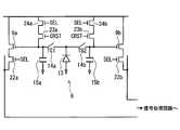
このような点に鑑み、反射光の受光状況や受光光学系の設計や画素の配置の制約を受けることなく、ダイナミックレンジを適切に拡張することができる光飛行型測距装置の実施形態について、以下説明する。図1に示すように、第1の実施形態に係る光飛行型測距装置1は、信号源2と、駆動回路3(駆動部)と、発光素子4と、制御回路5(制御部)と、受光素子6と、CM(コモンモード)成分除去回路7と、測距値取得回路8(測距値取得部)とを有する。測距値取得回路8は、バッファ9a,9bと、差分検出回路10と、AD変換回路11と、デジタル信号処理回路12とを有する。In view of such a point, the embodiment of the optical flight rangefinder capable of appropriately extending the dynamic range without being restricted by the reception status of reflected light, the design of the light receiving optical system and the arrangement of the pixels, This will be described below. As shown in FIG. 1, the optical flight type
信号源2は、駆動信号を駆動回路3及び制御回路5に出力することで、発光素子4と受光素子6との間で同期を確立し、発光素子4から発光される変調光に同期して受光素子6の露光を制御する。信号源2から出力される駆動信号は、発光素子4及び受光素子6を駆動する矩形パルス(通常数~数10MHz)であっても良いし、同期パルスのみであっても良い。発光素子4は、変調光としての例えば赤外光を発光するLD(Laser Diode)やLED(Light Emitting Diode)である。受光素子6は、例えばCMOS(Complementary Metal Oxide Semiconductor)やCCD(Charge Coupled Device)のプロセスを用いたイメージセンサである。The
受光素子6は、図2に示すように、PD(Photodiode)13と、2個の変調スイッチ14a,14bと、2個の蓄積容量15a,15bとを有する。2個の変調スイッチ14a,14bは、例えばMOSトランジスタやトランスファゲート等のMOS型のデバイス、CCD構造のデバイス等である。2個の蓄積容量15a,15bは、例えばMOS、CCD、MIM(Metal Insulator Metal)等の容量素子、配線、PN接合の寄生容量等である。受光素子6は、変調スイッチ14a,14bを制御信号(ゲート信号)TG1,TG2により駆動し、受光した入射光により発生する電荷を蓄積容量15a,15bに振り分け、振り分けた電荷の電荷量を示す信号をCM成分除去回路7に出力する。制御信号TG1,TG2は変調光に同期した信号であるので、自装置から対象物までの距離に応じて蓄積容量15a,15bに振り分けられる電荷の電荷量が変化する。図2では、2個の蓄積容量15a,15bを例示したが、3個以上の蓄積容量を設けても良い。As shown in FIG. 2, the
CM成分除去回路7は、発光している変調光に対して無視できない程度のレベルの背景光が存在する場合に、この背景光に起因して発生する電荷による画素の飽和を回避するものである。CM成分を除去する方法としては、先行文献で様々な技術が開示されている。例えば米国6919549B2号公報、独逸102005056774A1号公報、欧州1622200A1号公報等に開示されている。差分検出回路10は、CM成分除去回路7からバッファ9a,9bを介して入力した信号の差分を検出し、その検出した差分に応じた信号をAD変換回路11に出力する。バッファ9a,9bは、その簡素さから例えばソースフォロア回路により実現される。差分検出回路10は、例えば差動のアンプにより実現される。The CM
AD変換回路11は、差分検出回路10から入力した信号をアナログ信号からデジタル信号に変換してデジタル信号処理回路12に出力する。デジタル信号処理回路12は、AD変換回路11から入力した信号をデジタル信号処理し、蓄積容量15a,15bに振り分けられた電荷の電荷量から自装置から対象物までの距離を計算して測距値を取得する(測距する)。The
図3は、発光波形のデューティーを50%として4位相測距を行う(受光素子6を4位相で駆動する)場合のシーケンス(変調周期:Tm,露光期間:Tw)である。発光素子4から発光される変調光の波形(発光波形110)は、制御信号TG1,TG2と同期した矩形波で変調している。図3では矩形波で変調した場合を例示しているが、正弦波、三角波又は疑似ランダムシーケンス等の波形で変調しても良い。変調光が対象物で反射した反射光の波形(反射波形120)は、発光波形110に対して時間差を有するので、発光波形110に対して位相差φだけ遅れた波形となる。一方、制御信号TG1,TG2は180度ずつ位相が異なる矩形波で駆動される。デジタル信号処理回路12は、制御信号TG1-1,TG2-1(駆動波形111,121)で駆動するシーケンスを数十~数十万回程度の周期繰り返した後に、発生した電荷Q1、Q2の情報(電荷電圧変換された電圧値)を取得する。その後、デジタル信号処理回路12は、制御信号TG1-2,TG2-2(駆動波形112、122)で駆動するシーケンスを同様に数十~数十万回程度の周期繰り返した後に、発生した電荷Q3、Q4の情報を取得する。そして、デジタル信号処理回路12は、取得したQ1~Q4から離散フーリエ変換(DFT:Discrete Fourier Transform)を用いて位相差φの推定値θを以下の演算式(1)により計算する。FIG. 3 shows a sequence (modulation cycle: Tm, exposure period: Tw) in the case where four-phase ranging is performed with the duty of the light emission waveform set to 50% (the
θ=tan-1[(Q1-Q3)/(Q2-Q4)]…(1)
演算式(1)は上記4つのサンプリングに基づく位相差の演算式であるが、一般のN位相についても位相差φの推定値θ(以下、位相差θと称する)を以下の演算式(2)により計算することが可能である。θ = tan-1 [(Q1-Q3) / (Q2-Q4)] (1)
The calculation formula (1) is a calculation formula for the phase difference based on the above four samplings, but the estimated value θ of the phase difference φ (hereinafter referred to as the phase difference θ) for the general N phase is expressed by the following calculation formula (2 ).
θ=tan-1[(ΣQk*sin(2π/N*k))/(ΣQk*cos(2π/N*k))]…(2)
図4は、差動出力のシーケンスである。差分検出回路10は、制御信号TG1,TG2の組み合わせ、例えば制御信号TG1-1(駆動波形111),TG2-1(駆動波形121)を数十~数十万回繰り返してデジタル値D1(201)を生成する。同様にして、差分検出回路10は、制御信号TG1-2(駆動波形112),TG2-2(駆動波形122)からデジタル値D2(202)を生成し、制御信号TG1-3(駆動波形113),TG2-3(駆動波形123)からデジタル値D3(203)を生成し、制御信号TG1-4(駆動波形114),TG2-4(駆動波形124)からデジタル値D4(204)を生成する。この場合、差分検出回路10は、デジタル値D1~D4を、DC成分を除去した値として出力する。それぞれのデジタル値D1~D4について制御信号TG1が「H」であり且つTG2が「L」であるときに「1」を割り当て、制御信号TG1が「L」であり且つTG2が「H」であるときに「-1」を割り当てて記述する。即ち、Dxの波形について値が「1」及び「-1」の何れであるかにより、制御信号TG1,TG2の状態が一意に決定される。尚、このようにDxが2つの蓄積容量15a,15bの差分を示す信号であるので、AD変換回路11は、先述した演算式(1)の分子又は分母に相当する演算が実施された信号を出力する。θ = tan−1 [(ΣQk * sin (2π / N * k)) / (ΣQk * cos (2π / N * k))] (2)
FIG. 4 shows a differential output sequence. The
さて、このような位相型の光飛行型測距装置1を車載等で使用する場合、ダイナミックレンジの拡張が要求される。以下、本開示によるダイナミックレンジを拡張する手法について説明する。Now, when such a phase type optical
図5は、本開示の概念を示す。本開示は、前述した参考例の長時間蓄積の期間に相当する基本露光期間を複数のサブ露光期間に分割することで、短時間露光の測距値を取得すると共に、参考例の露光(長時間露光)と等価な長時間露光の測距値を取得する。図6は、参考例の4位相測距の露光を2分割のサブ露光で実現するシーケンスを示し、図7は、そのタイミングチャートを示す。サブ露光1,2をデューティーが25%の波形で駆動し、サブ露光1,2をそれぞれ数十~数十万回程度同じ回数繰り返し、サブ露光間で電荷をリセットせずに積算することで、参考例の露光と等価な電荷蓄積を実現する。このように分割した複数のサブ露光期間が1巡する期間内(1巡期間内)に蓄積された電荷の電荷量から短時間露光の測距値を取得する(高速に更新する)ことができる。又、複数回の1巡期間内に蓄積された電荷の電荷量を積算して長時間露光の測距値を取得することができる。即ち、1つの画素(同じ画素)に蓄積されている電荷(出力値)を読み出すタイミングを工夫することで、1つの画素から短時間露光の測距値と長時間露光の測距値との両方を取得することができ、ダイナミックレンジを拡張することができる。FIG. 5 shows the concept of the present disclosure. The present disclosure divides the basic exposure period corresponding to the long-time accumulation period of the reference example described above into a plurality of sub-exposure periods, thereby obtaining a short-range exposure distance value and the exposure (long) of the reference example. A distance measurement value of long exposure equivalent to (time exposure) is acquired. FIG. 6 shows a sequence for realizing the four-phase ranging exposure of the reference example by the sub-exposure divided into two, and FIG. 7 shows a timing chart thereof. By driving the
図8は、2つのサブ露光から測距値を取得する原理を示す。前提として、前述した図31に示した2容量/4位相測距を行う場合とは別に、4容量/4位相測距を行う場合(別の参考例)がある。参考例の4位相測距の露光を2分割のサブ露光で実現する図6のシーケンスと、別の参考例の4容量/4位相測距を行う場合のシーケンスとを比較すると、図6に示したサブ露光1は4容量/4位相測距を行うシーケンスの0度-180度の露光に相当し、サブ露光2は4容量/4位相測距を行うシーケンスの90度-270度に相当する。これは、4位相測距の位相差θを計算する以下の演算式(3)の分子と分母に相当する。FIG. 8 shows the principle of obtaining a distance measurement value from two sub-exposures. As a premise, there is a case of performing 4 capacity / 4 phase distance measurement (another reference example) separately from the case of performing 2 capacity / 4 phase distance measurement shown in FIG. FIG. 6 shows a comparison between the sequence of FIG. 6 in which the exposure of the four-phase ranging in the reference example is realized by the sub-exposure divided into two and the sequence in the case of performing the four-capacity / 4-phase ranging in another reference example. Sub-exposure 1 corresponds to an exposure of 0 to 180 degrees in a sequence for performing 4 volume / 4 phase ranging, and

図8は、サブ露光が4位相に基づく場合であったが、一般的なN(Nは自然数)位相についても同様の考え方が成立する。一般的に離散フーリエ変換の演算式は以下の演算式(4)で与えられる。FIG. 8 shows the case where the sub-exposure is based on four phases, but the same idea holds for a general N (N is a natural number) phase. In general, an arithmetic expression of the discrete Fourier transform is given by the following arithmetic expression (4).


4位相測距の露光を2分割のサブ露光で実現する図6のシーケンスにおいて、「0」を実現する方法としては、以下に示す例えば第1から第3の方法がある。In the sequence of FIG. 6 in which the exposure of the four-phase distance measurement is realized by the sub-exposure divided into two, the methods for realizing “0” include the following first to third methods, for example.
第1の方法では、図9に示すように、変調スイッチ14a,14bを同時にオンする期間、即ち、TG1,TG2の両方が「H」となる期間を設けて「0」を実現する。TG1,TG2の両方が「H」となる期間においてPD13に発生した電荷はQa,Qbに分かれて蓄積容量15a,15bに蓄積され、Qa,Qbは等しい値となる。そのため、この成分はCM成分除去回路7及び差分検出回路10でキャンセルされ、その結果、AD変換回路11は「0」を出力する。In the first method, as shown in FIG. 9, a period in which the modulation switches 14a and 14b are simultaneously turned on, that is, a period in which both TG1 and TG2 are “H” is provided to realize “0”. The charges generated in the
第2の方法では、図10に示すように、変調スイッチ14a,14bとは別の変調スイッチ14cを設け、変調スイッチ14a,14bを同時にオフし且つ別の変調スイッチ14cがオンする期間、即ち、TG1,TG2の両方が「L」となり且つTG3が「H」となる期間を設けて「0」を実現する。このTG1,TG2の両方が「L」となり且つTG3が「H」となる期間においてPD13に発生した電荷は固定電位(例えばVDD)に破棄される。In the second method, as shown in FIG. 10, a
第3の方法では、図11に示すように、Qa,Qbのうち一方を破棄し、2回分のサンプルを統合して「0」を実現する。即ち、TG2が「H」の期間に蓄積された電荷を破棄する周期と、TG1が「H」の期間に蓄積された電荷を破棄する周期とを統合する。上記した第1の方法ではTG1,TG2の両方を「H」とする期間を設ける必要があり、第2の方法ではTG1,TG2の両方を「L」とする期間を設ける必要があるが、第3の方法は、そのような期間を設ける必要はなく、TG1,TG2を互いに反転する制御を行えば良く、単純な制御で済む利点がある。In the third method, as shown in FIG. 11, one of Qa and Qb is discarded and “0” is realized by integrating two samples. That is, the period for discarding the charges accumulated during the period when TG2 is “H” and the period for discarding the charges accumulated during the period when TG1 is “H” are integrated. In the first method described above, it is necessary to provide a period in which both TG1 and TG2 are “H”. In the second method, it is necessary to provide a period in which both TG1 and TG2 are “L”. The
図12は、4位相測距の露光を4分割のサブ露光で実現するシーケンスを示す。この場合は、サブ露光をデューティーが12.5%の波形で起動することで、8容量/8位相測距と等価になる。図13は、4位相測距の露光を4分割のサブ露光で実現する別のシーケンスを示す。この場合は、サブ露光をデューティーが37.5%の波形で起動する。図12では長時間蓄積のSNR(信号対雑音比(signal-to-noise ratio))を参考例の方法と同等とするには、露光時間を4倍にする必要があるが、図13では、サブ露光において信号を積分している時間を図12に示すシーケンスよりも長くすることで、露光時間を4倍にする必要がなくSNRを改善することができる。図14は、4位相測距の露光を4分割のサブ露光で実現する更に別のシーケンスを示す。この場合は、サブ露光をデューティーが50%の波形で起動する。図12及び図13では「0」を挿入する制御を行う必要があるが、図14では、同じ露光時間で得られるSNRは図13に示すシーケンスよりも劣るが、「0」を挿入する制御を不要とすることができる。FIG. 12 shows a sequence for realizing 4-phase ranging exposure by sub-exposure divided into 4 parts. In this case, starting sub-exposure with a waveform having a duty of 12.5% is equivalent to 8-capacity / 8-phase ranging. FIG. 13 shows another sequence for realizing 4-phase distance measurement exposure by sub-exposure divided into 4 parts. In this case, the sub-exposure is started with a waveform having a duty of 37.5%. In FIG. 12, in order to make the SNR (signal-to-noise ratio) accumulated for a long time equivalent to the method of the reference example, the exposure time needs to be quadrupled, but in FIG. By making the signal integration time in the sub-exposure longer than the sequence shown in FIG. 12, the exposure time does not need to be quadrupled, and the SNR can be improved. FIG. 14 shows still another sequence for realizing the 4-phase distance measurement exposure by the sub-exposure divided into four. In this case, the sub-exposure is activated with a waveform having a duty of 50%. In FIG. 12 and FIG. 13, it is necessary to perform control for inserting “0”. In FIG. 14, the SNR obtained at the same exposure time is inferior to the sequence shown in FIG. It can be unnecessary.
図15は、受光素子6の後段である測距値取得回路8の一部を、アナログメモリを用いて構成する回路図を示し、図16は、その動作のタイミングチャートを示す。測距値取得回路8は、受光素子6(PD13、変調スイッチ14a,14b、蓄積容量15a,15b)に、バッファ9a,9b、リセット用のスイッチング素子21a,21b、セレクタ用のスイッチング素子22a,22bが接続されている。これらバッファ9a,9b、スイッチング素子21a,21b、スイッチング素子22a,22bは、例えば電界効果トランジスタ(FET:Field effect transistor)により構成されている。アナログ差動信号処理回路23は、受光素子6から電荷量を差動で読み出し、出力信号をアナログメモリ24及び差分計算回路25に出力する。アナログメモリ24は、アナログ差動信号処理回路23から出力信号を入力すると、その入力した出力信号の出力値を保持し、次の出力信号を入力すると、保持している出力値を含む出力信号を差分計算回路25に出力する。差分計算回路25は、アナログ差動信号処理回路23から入力した出力信号の出力値からアナログメモリ24から入力した出力信号の出力値を差し引いて差分を計算して出力する。即ち、測距値取得回路8は、アナログ差動信号処理回路23から直接出力する出力信号を長時間露光の測距値として出力し、差分計算回路25から出力する出力信号を短時間露光の測距値として出力する。このようなアナログ回路で差分を計算する構成では、後述するデジタル回路で差分を計算する構成と比べ、回路面積の増大やノイズの影響が問題となるが、量子化誤差の影響を抑えることができる。FIG. 15 shows a circuit diagram in which a part of the distance measurement
図17は、受光素子6の後段である測距値取得回路8の一部を、デジタルメモリを用いて構成する回路図を示し、図18は、その動作のタイミングチャートを示す。AD変換回路11は、受光素子6から電荷量を差動で読み出してAD変換し、出力信号をデジタルメモリ31及び差分計算回路32に出力する。デジタルメモリ31は、AD変換回路11から出力信号を入力すると、その入力した出力信号の出力値を保持し、次の出力信号を入力すると、保持している出力値を含む出力信号を差分計算回路32に出力する。差分計算回路32は、AD変換回路11から入力した出力信号の出力値からデジタルメモリ31から入力した出力信号の出力値を差し引いて差分を計算して出力する。即ち、測距値取得回路8は、AD変換回路11から直接出力する出力信号を長時間露光の測距値として出力し、差分計算回路32から出力する出力信号を短時間露光の測距値として出力する。このようなデジタル回路で差分を計算する構成では、前述したアナログ回路で差分を計算する構成と比べ、量子化誤差の影響が問題となるが、回路面積及びノイズの影響を抑制することができる。FIG. 17 shows a circuit diagram in which a part of the distance measurement
次に、サブ露光の制御及び長時間露光の制御について説明する。Next, sub-exposure control and long-time exposure control will be described.
図19は、ローリングリセット及びローリング読み出しを行うタイミングチャートを示す。図19のタイミングチャートでは、どの行も読み出さない時間(露光時間調整用の時間)を設けているので、長時間蓄積の時間は読み出し行数の倍数である必要はない。又、画素毎の容量をもって長時間露光で得られる電荷を蓄積しているので、図15で示したアナログ差動信号処理回路23及びアナログメモリ24や図17で示したAD変換回路11やデジタルメモリ31はカラム毎に設ければ良くなる。FIG. 19 shows a timing chart for performing rolling reset and rolling reading. In the timing chart of FIG. 19, since a time during which no rows are read (exposure time adjustment time) is provided, the long-time accumulation time does not need to be a multiple of the number of read rows. Further, since charges obtained by long exposure with a capacity for each pixel are accumulated, the analog differential
図20は、ローリングリセット及びローリング読み出しを行う別のタイミングチャートを示す。前述した図19のタイミングチャートでは、サブ露光のシーケンスをローリングシャッタの露光時間の前後で止めていたが、周辺の画素に電荷が流れこむ等の影響が起きない場合には、露光をグローバルに同じ駆動波形で実施し、読み出しのみをローリングリセットで実現しても良い。FIG. 20 shows another timing chart for performing rolling reset and rolling reading. In the timing chart of FIG. 19 described above, the sub-exposure sequence is stopped before and after the exposure time of the rolling shutter. However, when there is no influence such as charge flowing into surrounding pixels, the exposure is the same globally. It may be implemented with a driving waveform, and only reading may be realized by rolling reset.
図21は、グローバルリセット及びローリング読み出しを行うタイミングチャートを示す。グローバルリセットでは全ての画素の値をメモリに保持する必要があるので、回路規模が増大するが、列毎に露光の同時性が担保されないことに伴う問題(所謂フォーカルプレーン歪み)を抑制することができる。FIG. 21 shows a timing chart for performing global reset and rolling readout. Since the global reset requires that all pixel values be held in the memory, the circuit scale increases, but it is possible to suppress problems (so-called focal plane distortion) associated with the inability to guarantee the simultaneity of exposure for each column. it can.
図22は、グローバルリセット及びローリング読み出しを行う別のタイミングチャートを示す。長時間蓄積についてはグローバルシャッタとし、短時間蓄積についてはローリングシャッタとすることで、長時間蓄積側についてはほぼフォーカルプレーン歪みのない出力を取得することができる。又、この場合も、図15で示したアナログ差動信号処理回路23及びアナログメモリ24や図17で示したAD変換回路11やデジタルメモリ31はカラム毎に設ければ良くなる。FIG. 22 shows another timing chart for performing global reset and rolling readout. By using a global shutter for long-time storage and a rolling shutter for short-time storage, an output with almost no focal plane distortion can be obtained on the long-time storage side. Also in this case, the analog differential
図23は、グローバルリセット及びローリング読み出しを行う更に別のタイミングチャートを示す。画素の読み出し時間により、サブ露光側のフレームレートが律則されてしまう場合は、サブ露光のローリングシャッタを間引きして読み出すことで、フレームレートを高めることができる。自装置から対象物までの距離が近かったり対象物が高反射率の物体であったりする場合には複数行に跨って計測される可能性が高いので、このように構成としても問題になり難い。FIG. 23 shows still another timing chart for performing global reset and rolling readout. When the frame rate on the sub-exposure side is regulated by the pixel readout time, the frame rate can be increased by thinning out the sub-exposure rolling shutter. If the distance from the device to the target is close or the target is a highly reflective object, there is a high possibility that the measurement will be performed across multiple lines. .
次に、長時間蓄積の出力の画素毎の振幅(読み出した出力値)を最適とする制御について説明する。Next, control for optimizing the amplitude (readout output value) for each pixel of the output accumulated for a long time will be described.
図24は、長時間蓄積の出力の画素毎の振幅を最適とするタイミングチャートを示す。図24の例示では、2行目を除く行の画素については、2巡目の読み出しを行った際に振幅が不十分であったので、更に露光を繰り返しているが、2行目の画素については、2巡目の読み出しを行った際に振幅が十分であったので、2巡目で露光を止めている。露光の制御線は行で共通であるので、該当する行の平均値、最大値又は最小値を用いて振幅が十分であるか否かを判定する。FIG. 24 is a timing chart for optimizing the amplitude for each pixel of the output accumulated for a long time. In the example of FIG. 24, since the amplitude of the pixels in the rows other than the second row was insufficient when the second round reading was performed, the exposure was further repeated. Since the amplitude was sufficient when reading was performed in the second round, the exposure was stopped in the second round. Since the exposure control line is common to the rows, the average value, maximum value, or minimum value of the corresponding row is used to determine whether the amplitude is sufficient.
図25は、長時間蓄積の出力の画素毎の振幅を最適とする別のタイミングチャートを示す。サブ露光の出力値が高い画素について画素毎にリセットを挿入することで、最終的な長時間露光の電荷が飽和しないように制御する。図25の例示では、2行目の画素についてリセットを挿入している。FIG. 25 shows another timing chart for optimizing the amplitude for each pixel of the output accumulated for a long time. By inserting a reset for each pixel for a pixel having a high sub-exposure output value, control is performed so that the final long-time exposure charge is not saturated. In the example of FIG. 25, reset is inserted for the pixels in the second row.
図26は、長時間蓄積の出力の画素毎の振幅を最適とする更に別のタイミングチャートを示す。前述した図25はローリングリセットを適用している場合であるが、グローバルリセットを適用している場合についても、サブ露光の出力値が高い画素について画素毎にリセットを挿入しても良い。FIG. 26 shows still another timing chart for optimizing the amplitude for each pixel of the output accumulated for a long time. FIG. 25 described above is a case where the rolling reset is applied, but also when the global reset is applied, a reset may be inserted for each pixel with respect to a pixel having a high sub-exposure output value.
図27は、画素毎にアダプティブにリセットを可能とする回路図を示し、図28は、その配線を示す。この場合、測距値取得回路8は、受光素子6に、バッファ9a,9b、リセット用のスイッチング素子21a,21b、セレクタ用のスイッチング素子22a,22bに加え、カラムリセット用のスイッチング素子23a,23b、セレクタ用のスイッチング素子24a,24bが接続されている。図25及び図26に示したシーケンスにおいて、露光制御の制御線を行内で共通とする構成を維持したままで画素毎にリセットするか否かを選択可能となる。SEL線とCRST線を共に「H」とすることで、その画素のみのリセットを行えるので、読み出し中の行のうち振幅が大の画素のみリセットすることができる。FIG. 27 shows a circuit diagram that enables adaptive reset for each pixel, and FIG. 28 shows the wiring thereof. In this case, the distance measurement
図29は、画素毎にアダプティブにリセット可能とする別の回路図を示し、図30は、その配線を示す。図27の構成で全てのCRST線を同時に「H」とすることで行毎のリセットを行えるので、RST線は冗長となる。即ち、図29では、図27の構成におけるRST線を省いた構成としている。FIG. 29 shows another circuit diagram in which each pixel can be adaptively reset, and FIG. 30 shows its wiring. Since all the CRST lines are simultaneously set to “H” in the configuration of FIG. 27, the reset for each row can be performed, so that the RST lines become redundant. That is, in FIG. 29, the RST line in the configuration of FIG. 27 is omitted.
以上に説明したように第1の実施形態によれば、次に示す作用効果を得ることができる。As described above, according to the first embodiment, the following operational effects can be obtained.
光飛行型測距装置1において、参考例の長時間蓄積に相当する基本露光期間を複数のサブ露光期間に分割し、複数のサブ露光期間が1巡する期間内ではサブ露光期間内に蓄積された電荷をリセットせずに保持する。そして、1巡期間内に蓄積された電荷の電荷量から短時間露光の測距値を取得すると共に、複数回の1巡期間内に蓄積された電荷の電荷量を積算して長時間露光の測距値を取得することで、1つの画素(同じ画素)から長時間露光の測距値と短時間露光の測距値との両方を取得するようにした。これにより、反射光の受光状況や受光光学系の設計や画素の配置の制約を受けることなく、ダイナミックレンジを拡張することができる。特に自装置及び対象物のうち少なくとも何れかが移動する車載等の場合に好適となる。
(第2の実施形態)
次に、第2の実施形態に係る飛行型測距装置について、以下説明する。In the
(Second Embodiment)
Next, the flight type distance measuring device according to the second embodiment will be described below.
先ず始めに、第2の実施形態の飛行型測距装置の技術的意義についての理解のため、図54~図56に示す比較例を用いて、多重露光を行う場合について説明する。図54及び図55に示すように、受光素子1101がPD(Photodiode)1102と、2個の変調スイッチ1103a,1103bと、1個の蓄積容量1104とを有する構成であり、4位相測距を行う場合を一例として説明する。この場合、図56に示すように、例えば画素Aの画素グループが1000回の駆動を繰り返して長時間露光を行い、画素Bの画素グループが100回の駆動を繰り返して短時間露光を行うことで、ダイナミックレンジを20dB拡張することができる。First, in order to understand the technical significance of the flight-type distance measuring device of the second embodiment, a case where multiple exposure is performed will be described using comparative examples shown in FIGS. As shown in FIGS. 54 and 55, the
この比較例では、面内の複数の画素を、長時間露光を行う画素グループと短時間露光を行う画素グループとに区分することで、多重露光をシリーズで行う場合よりもフレームレートが高められている。しかしながら、長時間露光と同様に短時間露光でも4位相測距であれば0度、90度、180度、270度のそれぞれの値を読み出した後に距離を計算するので、短時間露光のフレームレートが長時間露光の時間に律則することになる。このように比較例に係る方法では、短時間露光のフレームレートを高めることに限界がある。In this comparative example, by dividing a plurality of in-plane pixels into a pixel group that performs long exposure and a pixel group that performs short exposure, the frame rate can be increased compared to the case where multiple exposure is performed in series. Yes. However, in the case of four-phase ranging even in short exposure as in the case of long exposure, the distance is calculated after reading out the values of 0 degree, 90 degrees, 180 degrees, and 270 degrees, so the frame rate of the short exposure Will be governed by the long exposure time. As described above, the method according to the comparative example has a limit in increasing the frame rate of the short-time exposure.
このような点に鑑み、ダイナミックレンジを適切に拡張することができ、かつ短時間露光のフレームレートを適切に高めることができる第2の実施形態の光飛行型測距装置について、図34~図45を参照して以下詳細に説明する。In view of these points, the optical flight rangefinder of the second embodiment that can appropriately expand the dynamic range and can appropriately increase the frame rate of short-time exposure is shown in FIGS. 45 will be described in detail below.
第2の実施形態はシングルエンド出力の構成である。光飛行型測距装置201は、信号源202と、駆動回路203(駆動部)と、発光素子204と、制御回路205(制御部)と、受光素子206と、測距値取得回路207(測距値取得部)とを有する。測距値取得回路207は、バッファ208と、AD変換回路209と、デジタル信号処理回路210とを有する。The second embodiment has a single-ended output configuration. The optical flight type
信号源202は、駆動信号を駆動回路203及び制御回路205に出力することで、発光素子204と受光素子206との間で同期を確立し、発光素子204から発光される変調光に同期して受光素子206の露光を制御する。信号源202から出力される駆動信号は、発光素子204及び受光素子206を駆動する矩形パルス(通常数~数10MHz)であっても良いし、同期パルスのみであっても良い。発光素子204は、変調光としての例えば赤外光を発光するLD(Laser Diode)やLED(Light Emitting Diode)である。受光素子206は、例えばCMOS(Complementary Metal Oxide Semiconductor)やCCD(Charge Coupled Device)のプロセスを用いたイメージセンサである。The
受光素子206は、図35に示すように、PD(Photodiode)211と、2個の変調スイッチ212a,212bと、1個の蓄積容量213とを有する。2個の変調スイッチ212a,212bは、例えばMOSトランジスタやトランスファゲート等のMOS型のデバイス、CCD構造のデバイス等である。蓄積容量213は、例えばMOS、CCD、MIM(Metal Insulator Metal)等の容量素子、配線、PN接合の寄生容量等である。受光素子206は、変調スイッチ212a,212bを制御信号(ゲート信号)TG1により駆動し、受光した入射光により発生する電荷を蓄積容量213に蓄積し、電荷の電荷量を示す信号を測距値取得回路207に出力する。制御信号TG1は変調光に同期した信号であるので、自装置から対象物までの距離に応じて蓄積容量213に蓄積される電荷の電荷量が変化する。As shown in FIG. 35, the
バッファ208は、その簡素さから例えばソースフォロア回路により実現される。AD変換回路209は、バッファ208から入力した信号をアナログ信号からデジタル信号に変換してデジタル信号処理回路210に出力する。デジタル信号処理回路210は、AD変換回路209から入力した信号をデジタル信号処理し、蓄積容量213に蓄積された電荷の電荷量から自装置から対象物までの距離を計算して測距値を取得する(測距する)。The
図36は、発光波形のデューティーを50%として4位相測距を行う(受光素子206を4位相で駆動する)場合のシーケンス(変調周期:Tm,露光期間:Tw)を示す。発光素子204から発光される変調光の波形(発光波形2110)は、制御信号TG1と同期した矩形波で変調している。図36では矩形波で変調した場合を例示しているが、正弦波、三角波又は疑似ランダムシーケンス等の波形で変調しても良い。変調光が対象物で反射した反射光の波形(反射波形2120)は、発光波形2110に対して時間差を有するので、発光波形2110に対して位相差θだけ遅れた波形となる。一方、制御信号TG1は90度ずつ位相が異なる矩形波で駆動される。デジタル信号処理回路210は、制御信号TG1-1,TG1-2(駆動波形2111,2112)で駆動するシーケンスを数十~数十万回程度の周期繰り返した後に、発生した電荷Q1、Q2の情報(電荷電圧変換された電圧値)を取得する。その後、デジタル信号処理回路210は、制御信号TG1-3,TG1-4(駆動波形2113、2114)で駆動するシーケンスを同様に数十~数十万回程度の周期繰り返した後に、発生した電荷Q3、Q4の情報を取得する。そして、デジタル信号処理回路210は、取得したQ1~Q4から離散フーリエ変換(DFT:Discrete Fourier Transform)を用いて位相差θを第1の実施形態で説明したの演算式(1)により計算する。FIG. 36 shows a sequence (modulation cycle: Tm, exposure period: Tw) in the case where four-phase ranging is performed with the duty of the light emission waveform being 50% (the
さて、このような位相型の光飛行型測距装置201を車載等で使用する場合、ダイナミックレンジの拡張が要求されると共に、短時間露光のフレームレートの向上が要求される。以下、本開示によるダイナミックレンジを拡張しつつ、短時間露光のフレームレートを高める手法について説明する。Now, when such a phase-type optical
図37は、本開示のシングルエンド出力の構成において多重露光のタイミングチャートを示す。前述した図56に示した比較例の多重露光のタイミングチャートと比較すると、本開示の多重露光では、制御回路205は、面内の複数の画素を画素Aの画素グループと画素Bの画素グループとに区分する点は同じである。しかしながら、本開示の多重露光では、制御回路205は、画素Aの画素グループで長時間露光を行う期間内に、画素Bの画素グループで単一位相ではなく複数位相で電荷の蓄積と読み出しを行うことで、複数回の短時間露光を行う。その結果、画素Bの画素グループについては、同一期間で対比すると比較例の多重露光よりも測距値を取得する回数が増大し、測距値を頻繁に更新することができ、フレームレートを高めることができる。図37の例示では、画素Aの画素グループが1回の長時間露光を行う期間内に、画素Bの画素グループが4回の短時間露光を行うことで、図56のタイミングチャートで駆動する場合に対して4倍のフレームレートを実現することができる。このような短時間露光で取得可能な有効な値(十分な信号振幅)は自装置からの距離が近いか又は高反射率の対象物で反射した反射光によるものであるので、自装置からの距離が近いか又は高反射率の対象物に対してフレームレートを高めることができる。即ち、特に車載等のように対象物(人、車両、壁等)への衝突を回避するために距離を頻繁に計算する(フレームレートを高める)ことが要求される環境で好適である。FIG. 37 is a timing chart of multiple exposure in the single-ended output configuration of the present disclosure. Compared with the multiple exposure timing chart of the comparative example shown in FIG. 56 described above, in the multiple exposure according to the present disclosure, the
図38は、シングルエンド出力の構成の別の多重露光のタイミングチャートを示す。前述した図37では長時間露光と短時間露光とのフレームレートの比が「4」であるが、フレームレートの比は「4」に限らない。即ち、長時間露光に対する短時間露光のサイクル数(繰り返し回数)を増やすことで、フレームレートをより高めることができる。図38の例示では、図56のタイミングチャートで駆動する場合に対して12倍のフレームレートを実現することができ、図37のタイミングチャートで駆動する場合に対して3倍のフレームレートを実現することができる。逆に後段の信号処理の観点等から長時間露光に対する短時間露光のサイクル数を減らす(間引く)ことで、フレームレートを下げることができる。FIG. 38 shows another multiple exposure timing chart having a single-ended output configuration. In FIG. 37 described above, the frame rate ratio between the long time exposure and the short time exposure is “4”, but the frame rate ratio is not limited to “4”. That is, the frame rate can be further increased by increasing the number of short-time exposure cycles (the number of repetitions) with respect to the long-time exposure. In the example of FIG. 38, a
図39は、シングルエンド出力の構成の更に別の多重露光のタイミングチャートを示す。前述した図37及び図38では長時間露光の位相毎の期間内に短時間露光で測距値を1回以上取得したが、長時間露光の複数位相に跨る期間内に短時間露光で測距値を1回取得しても良い。図39の例示では、図56のタイミングチャートで駆動する場合に対して2倍のフレームレートを実現することができる。FIG. 39 shows still another multiple exposure timing chart having a single-end output configuration. In FIG. 37 and FIG. 38 described above, the distance measurement value is acquired at least once by the short exposure within the period of each phase of the long exposure, but the distance measurement is performed by the short exposure within the period extending over a plurality of phases of the long exposure. You may acquire a value once. In the example of FIG. 39, the frame rate can be doubled as compared with the case of driving with the timing chart of FIG.
図40及び図41は、面内の複数の画素を2つの画素グループに区分した配置形態を示す。図40では、長時間露光の画素グループAと短時間露光の画素グループBとを行毎に区分している。図40の構成では、変調スイッチ12a,12bを駆動する制御線の配線を共通とすることができ、既存の構成に大きな変更を加えずに短時間露光のフレームレートを高めることができる。一方、図41では、長時間露光の画素グループAと短時間露光の画素グループBとを市松模様(チェック)に区分している。図41の構成では、制御線の配線を増やす必要が生じるが、短時間露光を行う画素グループのみで画像を構成した場合に空間解像度を高めることができる。40 and 41 show an arrangement form in which a plurality of pixels in a plane are divided into two pixel groups. In FIG. 40, the long exposure pixel group A and the short exposure pixel group B are divided for each row. In the configuration of FIG. 40, the wiring of the control lines for driving the modulation switches 12a and 12b can be made common, and the frame rate for short-time exposure can be increased without greatly changing the existing configuration. On the other hand, in FIG. 41, the long exposure pixel group A and the short exposure pixel group B are divided into a checkered pattern (check). In the configuration of FIG. 41, it is necessary to increase the number of control lines, but the spatial resolution can be increased when an image is configured with only pixel groups that perform short-time exposure.
図42は、長時間露光の画素グループと短時間露光の画素グループとを時間で切り替える態様を示す。自装置からの距離が遠いか又は低反射率の対象物で反射した反射光は場合によっては1画素にしか受光されない可能性がある。そのため、長時間露光の画素グループと短時間露光の画素グループとを固定してしまうと、いつまでも測距値を取得することができない対象物が出現する可能性がある。この点に関し、長時間露光の画素グループと短時間露光の画素グループとを時間(例えばフレーム単位)で切り替えることで、上記した問題の発生を未然に回避することができる。図42の例示は、図40に示した長時間露光の画素グループと短時間露光の画素グループとを行毎に区分している構成において切り替える態様であるが、図41に示した長時間露光の画素グループと短時間露光の画素グループとを市松模様に区分している構成においても同様に切り替えることが可能である。FIG. 42 shows a mode in which a long exposure pixel group and a short exposure pixel group are switched over time. There is a possibility that reflected light reflected by an object having a long distance from the apparatus or having a low reflectance is received by only one pixel in some cases. Therefore, if the long-exposure pixel group and the short-exposure pixel group are fixed, there is a possibility that an object for which a distance measurement value cannot be obtained will appear. In this regard, the occurrence of the above-described problem can be avoided in advance by switching the long exposure pixel group and the short exposure pixel group by time (for example, in units of frames). The example of FIG. 42 is a mode in which the long exposure pixel group and the short exposure pixel group shown in FIG. 40 are switched in the configuration divided for each row, but the long exposure shown in FIG. It is possible to switch similarly in the configuration in which the pixel group and the short-time exposure pixel group are divided into a checkered pattern.
図43は、シングルエンド出力の構成の更に別の多重露光のタイミングチャートを示す。前述した図37から図39では面内の画素を2つの画素グループに区分したが、3つの画素グループに区分しても良い。図43の例示では、中時間露光を行う画素Bの画素グループでは、長時間露光を行う画素Aの画素グループに対して4倍のフレームレートを実現することができ、短時間露光を行う画素Cの画素グループでは、長時間露光を行う画素Aの画素グループに対して12倍のフレームレートを実現することができる。FIG. 43 shows still another multiple exposure timing chart having a single-ended output configuration. In FIG. 37 to FIG. 39 described above, the in-plane pixels are divided into two pixel groups, but may be divided into three pixel groups. In the example of FIG. 43, in the pixel group of the pixel B that performs medium-time exposure, the frame rate that is four times that of the pixel group of the pixel A that performs long-time exposure can be realized, and the pixel C that performs short-time exposure. In this pixel group, it is possible to realize a
図44及び図45は、面内の複数の画素を3つの画素グループ(一の画素グループ、第1の他の画素グループおよび第2の他の画素グループ)に区分した配置形態を示す。図44では、画素Cを全ての行に配置すると共に画素A及び画素Bをそれぞれ1行間隔で配置するように区分している。図44の構成では、1行あたりに必要な制御線の本数が全ての行で2種類となり、共通化し易くなり、画素Cの画素グループのみで画像を構成した場合に空間解像度を高めることができる。尚、画素Aを全ての行に配置すると共に画素B及び画素Cをそれぞれ1行間隔で配置するように区分しても良いし、画素Bを全ての行に配置すると共に画素A及び画素Cをそれぞれ1行間隔で配置するように区分しても良い。一方、図45では、画素A、画素B、画素Cを全ての行に配置するように区分している。図45の構成では、1行あたりに必要な制御線の本数が全ての行で3種類となり、共通化し難くなるが、画素A、画素B、画素Cの何れの画素グループのみで画像を構成した場合でも空間解像度を高めることができる。尚、このように面内の複数の画素を3つの画素グループに区分した場合でも、それぞれの画素グループを時間で切り替えても良い。44 and 45 show an arrangement in which a plurality of pixels in a plane are divided into three pixel groups (one pixel group, first other pixel group, and second other pixel group). In FIG. 44, the pixels C are arranged in all rows, and the pixels A and the pixels B are divided at intervals of one row. In the configuration of FIG. 44, the number of control lines required per row becomes two types in all the rows, and it becomes easy to share them, and the spatial resolution can be increased when an image is composed of only the pixel group of the pixel C. . The pixels A may be arranged in all rows and the pixels B and C may be divided at intervals of one row, or the pixels B may be arranged in all rows and the pixels A and C may be arranged. You may divide | segment so that it may arrange | position by 1 line interval, respectively. On the other hand, in FIG. 45, the pixels A, B, and C are divided so as to be arranged in all rows. In the configuration of FIG. 45, the number of control lines required per row is three types in all rows, making it difficult to share, but an image is configured only by any pixel group of pixel A, pixel B, and pixel C. Even in this case, the spatial resolution can be increased. Even when a plurality of pixels in the plane are divided into three pixel groups in this way, the respective pixel groups may be switched by time.
以上に説明したように第2の実施形態によれば、次に示す作用効果を得ることができる。光飛行型測距装置201において、面内の複数の画素を、長時間露光を行う画素グループと短時間露光を行う画素グループとに区分することで、ダイナミックレンジを拡張することができる。又、長時間露光を行う画素グループの受光素子が1回の長時間露光により測距値を1回取得する期間内に、短時間露光を行う画素グループの受光素子が複数回の短時間露光により測距値を複数回取得することで、短時間露光のフレームレートを高めることができる。これにより、ダイナミックレンジを適切に拡張することができつつ、短時間露光のフレームレートを適切に高めることができる。特に自装置及び対象物のうち少なくとも何れかが移動する車載等の場合に好適となる。As described above, according to the second embodiment, the following operational effects can be obtained. In the optical flight type
(第3の実施形態)
次に、本開示の第3の実施形態について、図46から図53を参照して説明する。尚、前述した第2の実施形態と同一部分については説明を省略し、異なる部分について説明する。第2の実施形態は、シングルエンド出力の構成であるが、第3の実施形態は、差動出力の構成である。光飛行型測距装置321は、信号源322と、駆動回路323(駆動部)と、発光素子324と、制御回路325(制御部)と、受光素子326と、CM(コモンモード)成分除去回路327と、測距値取得回路328(測距値取得部)とを有する。測距値取得回路328は、バッファ329a,329bと、差分検出回路330と、AD変換回路331と、デジタル信号処理回路332とを有する。(Third embodiment)
Next, a third embodiment of the present disclosure will be described with reference to FIGS. 46 to 53. In addition, description is abbreviate | omitted about the same part as 2nd Embodiment mentioned above, and a different part is demonstrated. The second embodiment has a single-ended output configuration, while the third embodiment has a differential output configuration. The
信号源322、駆動回路323、発光素子324及び制御回路325は、それぞれ第2の実施形態で説明した信号源202、駆動回路203、発光素子204及び制御回路205と同等である。受光素子326は、図47に示すように、3PD41と、2個の変調スイッチ342a,342bと、2個の蓄積容量343a,343bとを有する。受光素子326は、変調スイッチ342a,342bを制御信号TG1,TG2により駆動し、受光した入射光により発生する電荷を蓄積容量343a,343bに振り分けて蓄積し、電荷の電荷量を示す信号をCM成分除去回路327に出力する。制御信号TG1,TG2は変調光に同期した信号であるので、自装置から対象物までの距離に応じて蓄積容量343a,343bに振り分けられて蓄積される電荷の電荷量が変化する。図47では、2個の蓄積容量343a,343bを例示したが、3個以上の蓄積容量を設けても良い。The
CM成分除去回路327は、発光している変調光に対して無視できない程度のレベルの背景光が存在する場合に、この背景光に起因して発生する電荷による画素の飽和を回避するものである。CM成分を除去する方法としては、先行文献で様々な技術が開示されている。例えば米国6919549B2号公報、独逸102005056774A1号公報、欧州1622200A1号公報等に開示されている。差分検出回路330は、CM成分除去回路327からバッファ329a,329bを介して入力した信号の差分を検出し、その検出した差分に応じた信号をAD変換回路331に出力する。差分検出回路330は、例えば差動のアンプにより実現される。The CM
AD変換回路331は、差分検出回路330から入力した信号をアナログ信号からデジタル信号に変換してデジタル信号処理回路332に出力する。デジタル信号処理回路332は、AD変換回路331から入力した信号をデジタル信号処理し、蓄積容量343a,343bに振り分けられて蓄積された電荷の電荷量から自装置から対象物までの距離を計算して測距値を取得する(測距する)。The
図48は、発光波形のデューティーを50%として4位相測距を行う(受光素子326を4位相で駆動する)場合のシーケンスを示す。差分検出回路330は、制御信号TG1,TG2の組み合わせ、例えば制御信号TG1-1(駆動波形3111),TG2-1(駆動波形3121)を数十~数十万回繰り返してデジタル値D1を生成する。同様にして、差分検出回路330は、制御信号TG1-2(駆動波形3112),TG2-2(駆動波形3122)を数十~数十万回繰り返してデジタル値D2を生成する。差分検出回路330は、デジタル値D1,D2を、DC成分を除去した値として出力する。それぞれのデジタル値D1,D2について制御信号TG1が「H」であり且つTG2が「L」であるときに「1」を割り当て、制御信号TG1が「L」であり且つTG2が「H」であるときに「-1」を割り当てて記述する。即ち、Dxの波形について値が「1」及び「-1」の何れであるかにより、制御信号TG1,TG2の状態が一意に決定される。尚、このようにDxが2つの蓄積容量343a,343bの差分を示す信号であるので、AD変換回路331は、先述した演算式(1)の分子又は分母に相当する演算が実施された信号を出力する。FIG. 48 shows a sequence in a case where four-phase ranging is performed with the duty of the light emission waveform being 50% (the
図49は、本開示の作動出力の構成において多重露光のタイミングチャートを示す。図49の例示では、画素Aの画素グループが1回の長時間露光を行う期間内に、画素Bの画素グループが6回の短時間露光を行うことで、長時間露光を行う画素Aの画素グループに対して6倍のフレームレートを実現することができる。FIG. 49 is a timing chart of multiple exposure in the configuration of the operation output of the present disclosure. In the example of FIG. 49, the pixel group of the pixel A that performs long-time exposure by the pixel group of the pixel B performing six short-time exposures within the period in which the pixel group of the pixel A performs one long-time exposure. A frame rate that is six times that of the group can be realized.
図50は、本開示の作動出力の別のシーケンスを示し、図51は、そのシーケンスに対応する多重露光のタイミングチャートを示す。前述した図48ではデジタル値D1,D2を生成するのみであったが、デジタル値D1,D2に加え、制御信号TG1-3(駆動波形3113),TG2-3(駆動波形3123)を数十~数十万回繰り返してデジタル値D3を生成し、制御信号TG1-4(駆動波形3114),TG2-4(駆動波形3124)を数十~数十万回繰り返してデジタル値D4を生成する。図51の例示では、画素Aの画素グループが1回の長時間露光を行う期間内に、画素Bの画素グループが4回の短時間露光を行うことで、長時間露光を行う画素Aの画素グループに対して4倍のフレームレートを実現することができる。又、回路のミスマッチを未然に回避することができ、ロバスト性を高めることができる。FIG. 50 shows another sequence of the operation output of the present disclosure, and FIG. 51 shows a timing chart of multiple exposure corresponding to the sequence. In FIG. 48 described above, only the digital values D1 and D2 are generated. However, in addition to the digital values D1 and D2, the control signals TG1-3 (drive waveform 3113) and TG2-3 (drive waveform 3123) are several tens to The digital value D3 is generated by repeating several hundred thousand times, and the digital value D4 is generated by repeating the control signals TG1-4 (drive waveform 3114) and TG2-4 (drive waveform 3124) several tens to several hundred thousand times. In the example of FIG. 51, the pixel group of the pixel A that performs long-time exposure by performing the short-time exposure four times for the pixel group of the pixel B within the period in which the pixel group of the pixel A performs one long-time exposure. Four times the frame rate can be realized for the group. In addition, circuit mismatch can be avoided, and robustness can be improved.
図52は、本開示の作動出力の更に別のシーケンスを示し、図53は、そのシーケンスに対応する多重露光のタイミングチャートを示す。長時間露光の位相数と短時間露光の位相数とは同一である必要はなく、異なっていても良い。図52及び図53の例示では、長時間露光を6位相測距で駆動し、短時間露光を4位相測距で駆動している。又、図52及び図53の例示では、長時間露光については「1」及び「-1」に加え、信号を積分しない期間である非積分期間を示す「0」を挿入することで、高次高調波に感度を持たせている。即ち、発光波形のデューティーを50%よりも短くすると、デューティーが短くなるにしたがって高次高調波の成分のエネルギーが増加する特性を利用し、長時間露光については、所定の高次高調波に感度を持たせて高次高調波の成分のエネルギーを有効に活用する。デジタル信号処理回路332は、基本波の成分と高次高調波の成分とを線形結合して距離を計算することで、高次高調波の成分を加味する分、基本波の成分のみから距離を計算する場合よりも距離誤差を低減することができる。尚、このような高次高調波に感度を持たせる技術について出願人は特願2014-226069号を出願している。FIG. 52 shows still another sequence of the operation output of the present disclosure, and FIG. 53 shows a timing chart of multiple exposure corresponding to the sequence. The number of phases for long exposure and the number of phases for short exposure need not be the same, and may be different. In the examples of FIGS. 52 and 53, long exposure is driven by 6-phase ranging, and short exposure is driven by 4-phase ranging. In the examples of FIGS. 52 and 53, in addition to “1” and “−1” for long exposure, “0” indicating a non-integration period which is a period in which the signal is not integrated is inserted, so Sensitivity is given to harmonics. That is, when the duty of the light emission waveform is made shorter than 50%, the characteristic that the energy of the higher-order harmonic component increases as the duty becomes shorter is used. For long-time exposure, sensitivity to a predetermined higher-order harmonic is used. To effectively utilize the energy of the higher harmonic components. The digital signal processing circuit 332 calculates the distance by linearly combining the fundamental wave component and the higher-order harmonic component, thereby adding the higher-order harmonic component and calculating the distance from only the fundamental wave component. The distance error can be reduced as compared with the case of calculation. Incidentally, the applicant has applied for Japanese Patent Application No. 2014-226069 regarding a technique for giving sensitivity to such high-order harmonics.
以上に説明したように第3の実施形態によれば、シングルエンド出力の構成に限らず、差動出力の構成でも前述した第2の実施形態と同様の作用効果を得ることができ、ダイナミックレンジを適切に拡張することができつつ、短時間露光のフレームレートを適切に高めることができる。尚、第3の実施形態でも、2つの画素グループに区分する構成に限らず、前述した第2の実施形態と同様に3つの画素グループに区分する構成としても良いし、それぞれの画素グループを時間で切り替えても良い。As described above, according to the third embodiment, not only the configuration of the single-end output but also the configuration of the differential output can obtain the same effects as those of the second embodiment described above, and the dynamic range. It is possible to appropriately increase the frame rate for short-time exposure. Note that the third embodiment is not limited to the configuration in which the pixel groups are divided into two pixel groups, and may be configured to be divided into three pixel groups as in the second embodiment described above. You can switch with.
(その他の実施形態)
本開示は、上記した実施形態にのみ限定されるものではなく、以下のように変形又は拡張することができる。(Other embodiments)
The present disclosure is not limited to the above-described embodiment, and can be modified or expanded as follows.
第1~第3の実施形態では、光飛行型測距装置を車両に用いた場合を示したが、本開示の飛行型測距装置を車載以外の用途に適用しても良い。In the first to third embodiments, the case where the optical flight type distance measuring device is used in a vehicle is shown, but the flight type distance measuring device of the present disclosure may be applied to uses other than in-vehicle use.
第2および第3の実施形態では、2つの画素グループや3つの画素グループに区分する構成を例示したが、露光期間が互いに異なる4つ以上の画素グループに区分する構成でも良い。又、4つ以上の画素グループに区分する場合でも、それぞれの画素グループを時間で切り替えても良い。In the second and third embodiments, the configuration of dividing into two pixel groups or three pixel groups is illustrated, but a configuration of dividing into four or more pixel groups having different exposure periods may be used. Even when the pixel group is divided into four or more pixel groups, each pixel group may be switched by time.
第2および第3の実施形態について、2つの画素グループに区分する場合の長時間露光と短時間露光のそれぞれの位相数の組み合わせや3つの画素グループに区分する場合の長時間露光と中時間露光と短時間露光のそれぞれの位相数の組み合わせはどのようであっても良い。又、4つ以上の画素グループに区分する場合でも同様にそれぞれの位相数の組み合わせはどのようであっても良い。
Regarding the second and third embodiments, combinations of the respective phase numbers of long exposure and short exposure when divided into two pixel groups, and long exposure and medium time exposure when divided into three pixel groups Any combination of phase numbers for short-time exposure may be used. Similarly, even when dividing into four or more pixel groups, any combination of the respective phase numbers may be used.
Claims (27)
Translated fromJapanese前記発光素子を駆動する駆動部(3)と、
変調光が対象物で反射した反射光を含む入射光に応じた電荷を複数の変調スイッチ(14a,14b)により振り分けて複数の蓄積容量(15a,15b)に蓄積する受光素子(6)と、
前記複数の変調スイッチの駆動を制御する制御部(5)と、
前記受光素子によりサンプリングされた値を用いて前記対象物までの距離を計算して測距値を取得する測距値取得部(8)と、を備え、
前記制御部は、基本露光期間を複数のサブ露光期間に分割するように前記複数の変調スイッチの駆動を制御し、複数のサブ露光期間が1巡する1巡期間内ではサブ露光期間内に蓄積された電荷をリセットせずに保持し、
前記測距値取得部は、前記1巡期間内に蓄積された電荷の電荷量から短時間露光の測距値を取得すると共に、複数回の前記1巡期間内に蓄積された電荷の電荷量を積算して長時間露光の測距値を取得する光飛行型測距装置。A light emitting element (4) for emitting modulated light modulated in a pattern having a repetition period into space;
A drive unit (3) for driving the light emitting element;
A light receiving element (6) that distributes charges according to incident light including reflected light, which is reflected from the object by the modulated light, by a plurality of modulation switches (14a, 14b) and accumulates them in a plurality of storage capacitors (15a, 15b);
A control unit (5) for controlling driving of the plurality of modulation switches;
A distance value acquisition unit (8) that calculates a distance to the object using a value sampled by the light receiving element and acquires a distance value; and
The control unit controls driving of the plurality of modulation switches so as to divide a basic exposure period into a plurality of sub-exposure periods, and accumulates within the sub-exposure period within one round period in which the plurality of sub-exposure periods make one round. Hold the charged charge without resetting,
The distance measurement value acquisition unit acquires a distance measurement value of short-time exposure from the charge amount of charge accumulated in the one round period, and the charge amount of charge accumulated in a plurality of times of the one round period. An optical flight-type distance measuring device that obtains distance values for long exposure by integrating
前記受光素子は、変調光が対象物で反射した反射光を含む入射光に応じた電荷を2つの変調スイッチにより振り分けて2つの蓄積容量に蓄積し、
前記制御部は、基本露光期間での基本露光パターンとして、前記2つの変調スイッチのうち一方を駆動する制御信号がHであり且つ他方を駆動する制御信号がLである期間を1と定義すると共に、一方を駆動する制御信号がLであり且つ他方を駆動する制御信号がHである期間を-1と定義し、サブ露光期間でのサブ露光パターンとして、1の期間と-1の期間とが180度位相がずれるように1の期間及び-1の期間をそれぞれn(nは2以上の自然数)分割し、1及び-1の何れでもない期間に0を挿入する光飛行型測距装置。In the optical flight type distance measuring device according to claim 1,
The light receiving element distributes charges according to incident light including reflected light, which is reflected from the object by modulated light, by two modulation switches, and accumulates them in two storage capacitors.
The control unit defines, as a basic exposure pattern in the basic exposure period, a period in which a control signal for driving one of the two modulation switches is H and a control signal for driving the other is L, as 1. , A period in which the control signal for driving one is L and the control signal for driving the other is H is defined as −1. As a sub-exposure pattern in the sub-exposure period, a period of 1 and a period of −1 are defined. An optical flight rangefinder that divides a period of 1 and a period of −1 by n (n is a natural number of 2 or more) so that the phase is shifted by 180 degrees, and inserts 0 in a period that is neither 1 nor −1.
前記制御部は、サブ露光パターンにおいて、前記2つの変調スイッチをそれぞれ駆動する制御信号が共にHである期間を設けることで、0を挿入する光飛行型測距装置。In the optical flight type distance measuring device according to claim 2,
The control unit is an optical flight-type distance measuring device in which 0 is inserted by providing a period in which both control signals for driving the two modulation switches are H in the sub-exposure pattern.
前記受光素子は、2つの変調スイッチとは別の変調スイッチ(14c)を有し、
前記制御部は、サブ露光パターンにおいて、前記2つの変調スイッチをそれぞれ駆動する制御信号が共にLであり且つ前記別の変調スイッチを駆動する制御信号がHである期間を設けることで、0を挿入する光飛行型測距装置。In the optical flight type distance measuring device according to claim 2,
The light receiving element has a modulation switch (14c) different from the two modulation switches,
The control unit inserts 0 in the sub-exposure pattern by providing a period in which both of the control signals for driving the two modulation switches are L and the control signal for driving the other modulation switch is H. Optical flight type distance measuring device.
前記制御部は、サブ露光パターンにおいて、前記2つの変調スイッチをそれぞれ駆動する制御信号を反転制御し、前記2つの蓄積容量のうち一方に蓄積された電荷を破棄する周期と、前記2つの蓄積容量のうち他方に蓄積された電荷を破棄する周期とを統合することで、0を挿入する光飛行型測距装置。In the optical flight type distance measuring device according to claim 2,
The control unit inverts control signals for driving the two modulation switches in a sub-exposure pattern, discards charges accumulated in one of the two storage capacitors, and the two storage capacitors. An optical flight-type distance measuring device that inserts 0 by integrating the period in which the charge accumulated in the other is discarded.
前記制御部は、サブ露光パターンにおいて、基本露光期間の周期をTとしたときに、1の期間及び-1の期間をそれぞれT/(2n)よりも長くする光飛行型測距装置。In the optical flight type distance measuring device according to any one of claims 2 to 5,
In the sub-exposure pattern, the control unit is an optical flight-type distance measuring device that sets a period of 1 and a period of −1 longer than T / (2n), where T is a period of a basic exposure period.
前記測距値取得部は、前記受光素子から電荷量を差動で読み出すアナログ差動信号処理回路(23)と、前記アナログ差動信号処理回路の出力値を保持するアナログメモリ(24)と、前記アナログ差動信号処理回路から現在の出力タイミングで出力された現在の出力値と前記アナログ差動信号処理回路から1つ前の出力タイミングで出力されて前記アナログメモリに保持されている1つ前の出力値との差分を計算する差分計算回路(25)と、を有する光飛行型測距装置。In the optical flight type distance measuring device according to any one of claims 1 to 6,
The ranging value acquisition unit includes an analog differential signal processing circuit (23) that differentially reads an amount of charge from the light receiving element, an analog memory (24) that holds an output value of the analog differential signal processing circuit, The current output value output from the analog differential signal processing circuit at the current output timing and the previous output value output from the analog differential signal processing circuit at the previous output timing and held in the analog memory An optical flight-type distance measuring device comprising: a difference calculation circuit (25) for calculating a difference from the output value of
前記測距値取得部は、スイッチトキャパシタ回路である光飛行型測距装置。In the optical flight type distance measuring device according to claim 7,
The distance measurement value acquisition unit is an optical flight type distance measuring device which is a switched capacitor circuit.
前記測距値取得部は、前記受光素子から電荷量を差動で読み出してAD変換するAD変換回路(11)と、前記AD変換回路の出力値を保持するデジタルメモリ(31)と、前記AD変換回路から現在の出力タイミングで出力された現在の出力値と前記AD変換回路から1つ前の出力タイミングで出力されて前記デジタルメモリに保持されている1つ前の出力値との差分を計算する差分計算回路(32)と、を有する光飛行型測距装置。In the optical flight type distance measuring device according to any one of claims 1 to 6,
The distance measurement value acquisition unit includes an AD conversion circuit (11) that differentially reads out the charge amount from the light receiving element and performs AD conversion, a digital memory (31) that holds an output value of the AD conversion circuit, and the AD The difference between the current output value output from the conversion circuit at the current output timing and the previous output value output from the AD conversion circuit at the previous output timing and held in the digital memory is calculated. An optical flight rangefinder having a difference calculation circuit (32).
前記制御部は、サブ露光の制御及び複数回のサブ露光を繰り返す長時間露光の制御の何れも、ローリングリセット及びローリング読み出しにより行う光飛行型測距装置。In the optical flight type distance measuring device according to any one of claims 1 to 9,
The control unit is an optical flight range finder that performs both sub-exposure control and long-time exposure control that repeats a plurality of sub-exposures by rolling reset and rolling readout.
前記制御部は、サブ露光の制御及び複数回のサブ露光を繰り返す長時間露光の制御の何れも、グローバルリセット及びローリング読み出しにより行う光飛行型測距装置。In the optical flight type distance measuring device according to any one of claims 1 to 9,
The control unit is an optical flight-type distance measuring device that performs both sub-exposure control and long-time exposure control that repeats a plurality of sub-exposures by global reset and rolling readout.
前記制御部は、行単位で読み出したサブ露光の出力値に応じてサブ露光を繰り返して行うか否かを選択する光飛行型測距装置。In the optical flight type distance measuring device according to claim 10 or 11,
The said control part is an optical flight type distance measuring device which selects whether subexposure is repeatedly performed according to the output value of the subexposure read per line.
前記制御部は、行単位で読み出したサブ露光の出力値に応じてサブ露光を繰り返して行うか否かを、その行で読み出した値の平均値、最大値及び最小値のうち何れかを用いて決定する光飛行型測距装置。The optical flight type distance measuring device according to claim 12,
The control unit uses one of an average value, a maximum value, and a minimum value of the values read in the row as to whether or not the sub-exposure is repeatedly performed according to the output value of the sub-exposure read in row units. Optical flight type distance measuring device to be determined.
前記制御部は、読み出した行のサブ露光の出力値に応じて画素毎にリセットを行う光飛行型測距装置。In the optical flight type distance measuring device according to any one of claims 10 to 13,
The said control part is a light flight type distance measuring device which resets for every pixel according to the output value of the subexposure of the read line.
前記発光素子を駆動する駆動部(203,323)と、
それぞれが面内の画素を構成し、変調光が対象物で反射した反射光を含む入射光を受光する複数の受光素子(206,326)と、
前記複数の受光素子における電荷の蓄積と前記複数の受光素子からの電荷の読み出しを制御する制御部(205,325)と、
前記複数の受光素子から前記制御部により読み出された電荷を用いて対象物までの距離を計算して測距値を取得する測距値取得部(207,328)と、を備え、
前記制御部は、前記複数の受光素子を幾つかの画素グループに区分し、一の画素グループに属する受光素子が1回の長時間露光を行うことで前記測距値取得部により測距値が1回取得される期間内に、他の画素グループに属する受光素子が複数回の短時間露光を行うことで前記測距値取得部により測距値が複数回取得されるように複数の受光素子の駆動を制御する光飛行型測距装置。A light emitting element (204, 324) that emits modulated light modulated in a pattern having a repetition period into space;
Driving units (203, 323) for driving the light emitting elements;
A plurality of light receiving elements (206, 326), each of which constitutes an in-plane pixel, and receives incident light including reflected light in which modulated light is reflected by an object;
A control unit (205, 325) for controlling charge accumulation in the plurality of light receiving elements and reading of charge from the plurality of light receiving elements;
A distance measurement value acquisition unit (207, 328) that calculates a distance to an object using charges read from the plurality of light receiving elements by the control unit and acquires a distance measurement value;
The control unit divides the plurality of light receiving elements into several pixel groups, and the distance measurement value is obtained by the distance measurement value acquiring unit when the light receiving elements belonging to one pixel group perform one long exposure. A plurality of light receiving elements so that a distance measurement value is acquired a plurality of times by the distance measurement value acquiring unit by performing light exposure elements belonging to another pixel group a plurality of short-time exposures within a period acquired once. Optical flight-type distance measuring device that controls the driving of the.
前記制御部は、一の画素グループに属する受光素子がn(nは2以上の自然数)位相を基本とするn回の電荷の蓄積とn回の電荷の読み出しを繰り返す1回の長時間露光を行う期間内に、他の画素グループに属する受光素子がn位相を基本とするn回の電荷の蓄積とn回の電荷の読み出しを繰り返す1回の短時間露光を複数回行うように、前記複数の受光素子の駆動を制御する光飛行型測距装置。In the optical flight type distance measuring device according to claim 15,
The control unit performs one long exposure in which light receiving elements belonging to one pixel group repeat n times of charge accumulation and n times of charge reading based on n (n is a natural number of 2 or more) phase. The plurality of light receiving elements belonging to the other pixel groups perform a plurality of times of short-time exposure that repeats n times of charge accumulation and n times of charge readout within a period of time. Optical distance measuring device for controlling the driving of the light receiving element.
前記制御部は、前記複数の受光素子の駆動を、デューティーが50%の矩形波形を2π/nずつずらした駆動波形を用いて制御する光飛行型測距装置。In the optical flight type distance measuring device according to claim 16,
The said control part is an optical flight type distance measuring device which controls the drive of these light receiving elements using the drive waveform which shifted the rectangular waveform with a 50% duty by 2 (pi) / n.
前記制御部は、一の画素グループに属する受光素子がn(nは2以上の自然数)位相を基本とするn回の電荷の蓄積とn回の電荷の読み出しを繰り返す1回の長時間露光を行う期間内に、他の画素グループに属する受光素子がm(mは2以上の自然数であり、nとは異なる値)位相を基本とするm回の電荷の蓄積とm回の電荷の読み出しを繰り返す1回の短時間露光を複数回行うように、前記複数の受光素子の駆動を制御する光飛行型測距装置。In the optical flight type distance measuring device according to claim 15,
The control unit performs one long exposure in which light receiving elements belonging to one pixel group repeat n times of charge accumulation and n times of charge reading based on n (n is a natural number of 2 or more) phase. Within a period of time, light receiving elements belonging to other pixel groups perform m charge accumulation and m charge readout based on m (m is a natural number of 2 or more and a value different from n) phase. An optical flight-type distance measuring device that controls driving of the plurality of light receiving elements so that repeated short-time exposure is performed a plurality of times.
前記制御部は、一の画素グループに属する受光素子の駆動を、デューティーが50%の矩形波形を2π/nずつずらした駆動波形を用いて制御し、他の画素グループに属する受光素子の駆動を、デューティーが50%の矩形波形を2π/mずつずらした駆動波形を用いて制御する光飛行型測距装置。The optical flight type distance measuring device according to claim 18,
The control unit controls driving of the light receiving elements belonging to one pixel group using a driving waveform obtained by shifting a rectangular waveform having a duty of 50% by 2π / n, and drives the light receiving elements belonging to another pixel group. An optical flight-type distance measuring device that uses a driving waveform obtained by shifting a rectangular waveform with a duty of 50% by 2π / m.
前記測距値取得部(207)は、前記複数の受光素子(206)からシングルエンドで出力された値を用いて対象物までの距離を計算して測距値を取得する光飛行型測距装置。The optical flight type distance measuring device according to any one of claims 15 to 19,
The distance measurement value acquisition unit (207) calculates a distance to an object using values output from the plurality of light receiving elements (206) at a single end, and acquires a distance measurement value. apparatus.
前記測距値取得部(328)は、前記複数の受光素子(326)から差動で出力された値を用いて対象物までの距離を計算して測距値を取得する光飛行型測距装置。The optical flight type distance measuring device according to any one of claims 15 to 19,
The distance measurement value acquisition unit (328) calculates a distance to an object using values differentially output from the plurality of light receiving elements (326) and acquires a distance measurement value. apparatus.
前記制御部は、長時間露光を行う画素グループに属する受光素子が少なくとも1つの高次高調波に感度を有するように、長時間露光を行う画素グループに属する受光素子の駆動を制御し、
前記測距値取得部は、長時間露光を行う画素グループに属する受光素子については、基本波の成分と前記少なくとも1つの高次高調波の成分とを線形結合して測距値を取得する光飛行型測距装置。In the optical flight type distance measuring device according to claim 21,
The control unit controls driving of the light receiving elements belonging to the pixel group performing long exposure so that the light receiving elements belonging to the pixel group performing long exposure have sensitivity to at least one higher-order harmonic,
The distance measurement value acquisition unit obtains a distance measurement value by linearly combining a fundamental wave component and the at least one higher-order harmonic component for a light receiving element belonging to a pixel group that performs long-time exposure. Flight rangefinder.
前記制御部は、前記他の画素グループを1つとし、前記一の画素グループに属する受光素子と前記他の画素グループに属する受光素子とがそれぞれ1行間隔の行単位で配置されるように区分する光飛行型測距装置。The optical flight type distance measuring device according to any one of claims 15 to 22,
The control unit is configured so that the other pixel group is one, and the light receiving elements belonging to the one pixel group and the light receiving elements belonging to the other pixel group are arranged in units of one row. Optical flight type distance measuring device.
前記制御部は、前記他の画素グループを1つとし、前記一の画素グループに属する受光素子と前記他の画素グループに属する受光素子とがそれぞれ市松模様で配置されるように区分する光飛行型測距装置。The optical flight type distance measuring device according to any one of claims 15 to 22,
The said control part makes the said other pixel group one, and the light flight type which sorts so that the light receiving element which belongs to the said one pixel group, and the light receiving element which belongs to the said other pixel group may be arrange | positioned in a checkered pattern, respectively. Distance measuring device.
前記制御部は、前記他の画素グループを第1の他の画素グループと第2の他の画素グループとを含む2つとし、前記一の画素グループ、前記第1の他の画素グループおよび前記第2の他の画素グループの何れか1つの画素グループに属する受光素子が市松模様で配置され、残りの2つの画素グループにそれぞれ属する受光素子が市松模様の残りに1行間隔の行単位で配置されるように区分する光飛行型測距装置。The optical flight type distance measuring device according to any one of claims 15 to 22,
The control unit includes two other pixel groups including a first other pixel group and a second other pixel group, the one pixel group, the first other pixel group, and the first pixel group. The light receiving elements belonging to any one of the two other pixel groups are arranged in a checkered pattern, and the light receiving elements belonging to the remaining two pixel groups are arranged in the checkered pattern in a row unit at intervals of one line. Optical flight type distance measuring device that classifies as follows.
前記制御部は、前記他の画素グループを第1の他の画素グループと第2の他の画素グループとを含む2つとし、前記一の画素グループ、前記第1の他の画素グループおよび前記第2の他の画素グループの全ての画素グループが全ての行に配置されるように区分する光飛行型測距装置。The optical flight type distance measuring device according to any one of claims 15 to 22,
The control unit includes two other pixel groups including a first other pixel group and a second other pixel group, the one pixel group, the first other pixel group, and the first pixel group. An optical flight type distance measuring device that classifies so that all pixel groups of two other pixel groups are arranged in all rows.
前記制御部は、所定の受光素子が前記一の画素グループに属する期間と前記他の画素グループに属する期間とを切り替える光飛行型測距装置。In the optical flight type distance measuring device according to any one of claims 15 to 26,
The control unit is an optical flight type distance measuring apparatus that switches between a period in which a predetermined light receiving element belongs to the one pixel group and a period in which the predetermined light receiving element belongs to the other pixel group.
Priority Applications (2)
| Application Number | Priority Date | Filing Date | Title |
|---|---|---|---|
| US15/525,311US10422879B2 (en) | 2014-11-14 | 2015-11-12 | Time-of-flight distance measuring device |
| DE112015005163.5TDE112015005163B4 (en) | 2014-11-14 | 2015-11-12 | FLIGHT TIME DISTANCE MEASURING DEVICE |
Applications Claiming Priority (4)
| Application Number | Priority Date | Filing Date | Title |
|---|---|---|---|
| JP2014-231630 | 2014-11-14 | ||
| JP2014231630AJP6539990B2 (en) | 2014-11-14 | 2014-11-14 | Optical flight type distance measuring device |
| JP2014236484AJP6424581B2 (en) | 2014-11-21 | 2014-11-21 | Optical flight type distance measuring device |
| JP2014-236484 | 2014-11-21 |
Publications (1)
| Publication Number | Publication Date |
|---|---|
| WO2016075945A1true WO2016075945A1 (en) | 2016-05-19 |
Family
ID=55954047
Family Applications (1)
| Application Number | Title | Priority Date | Filing Date |
|---|---|---|---|
| PCT/JP2015/005649WO2016075945A1 (en) | 2014-11-14 | 2015-11-12 | Optical time-of-flight range-finding device |
Country Status (3)
| Country | Link |
|---|---|
| US (1) | US10422879B2 (en) |
| DE (1) | DE112015005163B4 (en) |
| WO (1) | WO2016075945A1 (en) |
Cited By (4)
| Publication number | Priority date | Publication date | Assignee | Title |
|---|---|---|---|---|
| JP2019504326A (en)* | 2016-02-08 | 2019-02-14 | 株式会社デンソー | Time-of-flight distance measuring apparatus and method for detecting multipath errors |
| WO2019050024A1 (en)* | 2017-09-11 | 2019-03-14 | パナソニックIpマネジメント株式会社 | Distance measuring method and distance measuring device |
| EP3550330A4 (en)* | 2016-11-29 | 2019-10-30 | Panasonic Intellectual Property Management Co., Ltd. | DISTANCE MEASURING DEVICE |
| US10964032B2 (en) | 2017-05-30 | 2021-03-30 | Photon Sports Technologies Ab | Method and camera arrangement for measuring a movement of a person |
Families Citing this family (20)
| Publication number | Priority date | Publication date | Assignee | Title |
|---|---|---|---|---|
| JP6823815B2 (en)* | 2015-12-08 | 2021-02-03 | パナソニックIpマネジメント株式会社 | Solid-state image sensor, distance measuring device and distance measuring method |
| WO2018131514A1 (en)* | 2017-01-13 | 2018-07-19 | ソニー株式会社 | Signal processing device, signal processing method, and program |
| EP3367130A1 (en)* | 2017-02-22 | 2018-08-29 | STMicroelectronics (Research & Development) Limited | Integration of depth map device for adaptive lighting control |
| US10914824B2 (en) | 2017-11-21 | 2021-02-09 | Analog Devices International Unlimited Company | Systems and methods for measuring a time of flight in a lidar system |
| CN109981992B (en)* | 2017-12-28 | 2021-02-23 | 周秦娜 | Control method and device for improving ranging accuracy under high ambient light change |
| US11079723B2 (en) | 2018-02-06 | 2021-08-03 | Integrated Device Technology, Inc. | Apparatus and methods for automatic time measurements |
| JP2019164039A (en)* | 2018-03-20 | 2019-09-26 | ソニーセミコンダクタソリューションズ株式会社 | Distance sensor and distance measurement device |
| JP7214363B2 (en)* | 2018-04-27 | 2023-01-30 | ソニーセミコンダクタソリューションズ株式会社 | Ranging processing device, ranging module, ranging processing method, and program |
| JP7426339B2 (en)* | 2018-08-02 | 2024-02-01 | ヌヴォトンテクノロジージャパン株式会社 | Imaging device, solid-state imaging device used therein, and imaging method |
| JP2022036339A (en)* | 2018-10-12 | 2022-03-08 | ソニーセミコンダクタソリューションズ株式会社 | Sensor fusion system, synchronization control device, and synchronization control method |
| EP3887779A1 (en) | 2018-11-30 | 2021-10-06 | Carrier Corporation | Magnetic trap suppression tank level sensor |
| US10855896B1 (en)* | 2018-12-13 | 2020-12-01 | Facebook Technologies, Llc | Depth determination using time-of-flight and camera assembly with augmented pixels |
| WO2020178920A1 (en) | 2019-03-01 | 2020-09-10 | 株式会社ブルックマンテクノロジ | Distance image capturing device and distance image capturing method using distance image capturing device |
| US11070757B2 (en)* | 2019-05-02 | 2021-07-20 | Guangzhou Tyrafos Semiconductor Technologies Co., Ltd | Image sensor with distance sensing function and operating method thereof |
| TWI874430B (en)* | 2019-08-29 | 2025-03-01 | 日商索尼半導體解決方案公司 | Distance measuring sensor, driving method thereof, and distance measuring module |
| US11205279B2 (en)* | 2019-12-13 | 2021-12-21 | Sony Semiconductor Solutions Corporation | Imaging devices and decoding methods thereof |
| CN111175774B (en)* | 2020-01-14 | 2022-09-09 | 炬佑智能科技(苏州)有限公司 | Control method of TOF sensor module |
| CN112492172B (en)* | 2020-12-04 | 2025-06-13 | 昆山丘钛光电科技有限公司 | A flight time measurement module, control method thereof and electronic equipment |
| KR20220158109A (en) | 2021-05-20 | 2022-11-30 | 삼성전자주식회사 | Depth sensor and method of operating the same |
| US20240062349A1 (en)* | 2022-08-19 | 2024-02-22 | Gm Cruise Holdings Llc | Enhanced high dynamic range pipeline for three-dimensional image signal processing |
Citations (22)
| Publication number | Priority date | Publication date | Assignee | Title |
|---|---|---|---|---|
| JP2002536629A (en)* | 1999-01-28 | 2002-10-29 | マキューアン テクノロジーズ リミテッド ライアビリティ カンパニー | Short pulse microwave transceiver |
| JP2003247809A (en)* | 2002-02-26 | 2003-09-05 | Olympus Optical Co Ltd | Distance information input device |
| JP2004538491A (en)* | 2001-08-06 | 2004-12-24 | シーメンス アクチエンゲゼルシヤフト | Method and apparatus for recording three-dimensional range images |
| JP2006523074A (en)* | 2003-04-11 | 2006-10-05 | カネスタ インコーポレイテッド | Method and system for differentially expanding the dynamic range of a sensor |
| JP2007121116A (en)* | 2005-10-28 | 2007-05-17 | Sharp Corp | Optical distance measuring device |
| JP2007281556A (en)* | 2006-04-03 | 2007-10-25 | Seiko Epson Corp | Imaging device, imaging apparatus, and imaging system |
| JP2008524562A (en)* | 2004-12-18 | 2008-07-10 | ライカ ジオシステムズ アクチェンゲゼルシャフト | Electronic measurement method |
| JP2009047661A (en)* | 2007-08-22 | 2009-03-05 | Hamamatsu Photonics Kk | Ranging device |
| JP2010025906A (en)* | 2008-07-24 | 2010-02-04 | Panasonic Electric Works Co Ltd | Distance image sensor |
| JP2010096730A (en)* | 2008-10-20 | 2010-04-30 | Honda Motor Co Ltd | Distance measuring system and distance measuring method |
| JP2013050310A (en)* | 2011-08-30 | 2013-03-14 | Stanley Electric Co Ltd | Distance image generation device |
| JP2013516913A (en)* | 2010-01-06 | 2013-05-13 | メサ・イメージング・アー・ゲー | Demodulation sensor with separate pixel array and storage array |
| JP2013093847A (en)* | 2011-10-25 | 2013-05-16 | Samsung Electronics Co Ltd | Three-dimensional image acquisition apparatus and method of calculating depth information in the three-dimensional image acquisition apparatus |
| JP2013175951A (en)* | 2012-02-27 | 2013-09-05 | Honda Motor Co Ltd | Pixel drive device and pixel drive method |
| JP2013534639A (en)* | 2010-07-16 | 2013-09-05 | マイクロソフト コーポレーション | Method and system for multiphase phase dynamic calibration of three-dimensional (3D) sensors in a time-of-flight system |
| JP2013257178A (en)* | 2012-06-11 | 2013-12-26 | Asahi Kasei Electronics Co Ltd | Semiconductor device, self-diagnostic system, on-vehicle device using them, and medical device |
| US20140125766A1 (en)* | 2012-11-06 | 2014-05-08 | David Cohen | Accumulating charge from multiple imaging exposure periods |
| JP5579893B2 (en)* | 2012-03-01 | 2014-08-27 | オムニヴィジョン テクノロジーズ インコーポレイテッド | Circuit configuration and method for time-of-flight sensors |
| WO2014132767A1 (en)* | 2013-02-28 | 2014-09-04 | 株式会社テクノロジーハブ | Range image sensor |
| JP5585903B2 (en)* | 2008-07-30 | 2014-09-10 | 国立大学法人静岡大学 | Distance image sensor and method for generating imaging signal by time-of-flight method |
| WO2014207992A1 (en)* | 2013-06-26 | 2014-12-31 | パナソニックIpマネジメント株式会社 | Distance measurement and imaging device and measurement method for same |
| WO2015190015A1 (en)* | 2014-06-09 | 2015-12-17 | パナソニックIpマネジメント株式会社 | Distance measuring device |
Family Cites Families (12)
| Publication number | Priority date | Publication date | Assignee | Title |
|---|---|---|---|---|
| DE3804352A1 (en) | 1988-02-12 | 1989-08-24 | Keiper Recaro Gmbh Co | ADJUSTMENT FOR SEATS |
| US7379100B2 (en) | 2004-02-12 | 2008-05-27 | Canesta, Inc. | Method and system to increase dynamic range of time-of-flight (TOF) and/or imaging sensors |
| EP1622200A1 (en) | 2004-07-26 | 2006-02-01 | CSEM Centre Suisse d'Electronique et de Microtechnique SA | Solid-state photodetector pixel and photodetecting method |
| US7417718B2 (en) | 2005-10-28 | 2008-08-26 | Sharp Kabushiki Kaisha | Optical distance measuring apparatus |
| DE102005056774B4 (en) | 2005-11-28 | 2014-12-24 | Pmdtechnologies Gmbh | TOF pixel and method of operation |
| JP5261104B2 (en) | 2008-09-26 | 2013-08-14 | 京セラ株式会社 | Circuit board and electronic device |
| JP5743390B2 (en)* | 2009-09-15 | 2015-07-01 | 本田技研工業株式会社 | Ranging device and ranging method |
| US8754939B2 (en) | 2009-11-09 | 2014-06-17 | Mesa Imaging Ag | Multistage demodulation pixel and method |
| US8698670B2 (en) | 2011-06-01 | 2014-04-15 | Panasonic Corporation | High speed high resolution wide range low power analog correlator and radar sensor |
| JP5781918B2 (en) | 2011-12-28 | 2015-09-24 | 浜松ホトニクス株式会社 | Distance measuring device |
| DE102013203088B4 (en) | 2013-02-25 | 2017-05-11 | pmdtechnologies ag | Time of flight camera system |
| JP6251492B2 (en) | 2013-05-21 | 2017-12-20 | ヱスビー食品株式会社 | Self-moisture heat sterilization method for spices and spices obtainable thereby |
- 2015
- 2015-11-12WOPCT/JP2015/005649patent/WO2016075945A1/enactiveIP Right Grant
- 2015-11-12USUS15/525,311patent/US10422879B2/enactiveActive
- 2015-11-12DEDE112015005163.5Tpatent/DE112015005163B4/enactiveActive
Patent Citations (22)
| Publication number | Priority date | Publication date | Assignee | Title |
|---|---|---|---|---|
| JP2002536629A (en)* | 1999-01-28 | 2002-10-29 | マキューアン テクノロジーズ リミテッド ライアビリティ カンパニー | Short pulse microwave transceiver |
| JP2004538491A (en)* | 2001-08-06 | 2004-12-24 | シーメンス アクチエンゲゼルシヤフト | Method and apparatus for recording three-dimensional range images |
| JP2003247809A (en)* | 2002-02-26 | 2003-09-05 | Olympus Optical Co Ltd | Distance information input device |
| JP2006523074A (en)* | 2003-04-11 | 2006-10-05 | カネスタ インコーポレイテッド | Method and system for differentially expanding the dynamic range of a sensor |
| JP2008524562A (en)* | 2004-12-18 | 2008-07-10 | ライカ ジオシステムズ アクチェンゲゼルシャフト | Electronic measurement method |
| JP2007121116A (en)* | 2005-10-28 | 2007-05-17 | Sharp Corp | Optical distance measuring device |
| JP2007281556A (en)* | 2006-04-03 | 2007-10-25 | Seiko Epson Corp | Imaging device, imaging apparatus, and imaging system |
| JP2009047661A (en)* | 2007-08-22 | 2009-03-05 | Hamamatsu Photonics Kk | Ranging device |
| JP2010025906A (en)* | 2008-07-24 | 2010-02-04 | Panasonic Electric Works Co Ltd | Distance image sensor |
| JP5585903B2 (en)* | 2008-07-30 | 2014-09-10 | 国立大学法人静岡大学 | Distance image sensor and method for generating imaging signal by time-of-flight method |
| JP2010096730A (en)* | 2008-10-20 | 2010-04-30 | Honda Motor Co Ltd | Distance measuring system and distance measuring method |
| JP2013516913A (en)* | 2010-01-06 | 2013-05-13 | メサ・イメージング・アー・ゲー | Demodulation sensor with separate pixel array and storage array |
| JP2013534639A (en)* | 2010-07-16 | 2013-09-05 | マイクロソフト コーポレーション | Method and system for multiphase phase dynamic calibration of three-dimensional (3D) sensors in a time-of-flight system |
| JP2013050310A (en)* | 2011-08-30 | 2013-03-14 | Stanley Electric Co Ltd | Distance image generation device |
| JP2013093847A (en)* | 2011-10-25 | 2013-05-16 | Samsung Electronics Co Ltd | Three-dimensional image acquisition apparatus and method of calculating depth information in the three-dimensional image acquisition apparatus |
| JP2013175951A (en)* | 2012-02-27 | 2013-09-05 | Honda Motor Co Ltd | Pixel drive device and pixel drive method |
| JP5579893B2 (en)* | 2012-03-01 | 2014-08-27 | オムニヴィジョン テクノロジーズ インコーポレイテッド | Circuit configuration and method for time-of-flight sensors |
| JP2013257178A (en)* | 2012-06-11 | 2013-12-26 | Asahi Kasei Electronics Co Ltd | Semiconductor device, self-diagnostic system, on-vehicle device using them, and medical device |
| US20140125766A1 (en)* | 2012-11-06 | 2014-05-08 | David Cohen | Accumulating charge from multiple imaging exposure periods |
| WO2014132767A1 (en)* | 2013-02-28 | 2014-09-04 | 株式会社テクノロジーハブ | Range image sensor |
| WO2014207992A1 (en)* | 2013-06-26 | 2014-12-31 | パナソニックIpマネジメント株式会社 | Distance measurement and imaging device and measurement method for same |
| WO2015190015A1 (en)* | 2014-06-09 | 2015-12-17 | パナソニックIpマネジメント株式会社 | Distance measuring device |
Non-Patent Citations (3)
| Title |
|---|
| S.G.NARASIMHAN ET AL.: "Enhancing Resolution Along Multiple Imaging Dimensions Using Assorted Pixels.", IEEE TRANSACTIONS ON PATTERN ANALYSIS AND MACHINE INTELLIGENCE, vol. 27, no. 4, April 2005 (2005-04-01), pages 518 - 530* |
| S.NAYAR ET AL.: "High Dynamic Range Imaging:Spatially Varying Pixel Exposures.", IEEE CONFERENCE ON COMPUTER VISION AND PATTERN RECOGNITION (CVPR, vol. 1, June 2000 (2000-06-01), pages 472 - 479* |
| TOMOO MITSUNAGA: "Spatially Varying Exposure: a Wide Dynamic Range Imaging Method", IPSJ SIG NOTES, COMPUTER VISION AND IMAGE MEDIA (CVIM, vol. 2005, no. 4, January 2005 (2005-01-01), pages 155 - 162* |
Cited By (4)
| Publication number | Priority date | Publication date | Assignee | Title |
|---|---|---|---|---|
| JP2019504326A (en)* | 2016-02-08 | 2019-02-14 | 株式会社デンソー | Time-of-flight distance measuring apparatus and method for detecting multipath errors |
| EP3550330A4 (en)* | 2016-11-29 | 2019-10-30 | Panasonic Intellectual Property Management Co., Ltd. | DISTANCE MEASURING DEVICE |
| US10964032B2 (en) | 2017-05-30 | 2021-03-30 | Photon Sports Technologies Ab | Method and camera arrangement for measuring a movement of a person |
| WO2019050024A1 (en)* | 2017-09-11 | 2019-03-14 | パナソニックIpマネジメント株式会社 | Distance measuring method and distance measuring device |
Also Published As
| Publication number | Publication date |
|---|---|
| US20170315238A1 (en) | 2017-11-02 |
| DE112015005163B4 (en) | 2025-02-06 |
| DE112015005163T5 (en) | 2017-07-27 |
| US10422879B2 (en) | 2019-09-24 |
Similar Documents
| Publication | Publication Date | Title |
|---|---|---|
| WO2016075945A1 (en) | Optical time-of-flight range-finding device | |
| CN109564287B (en) | Optical flight type distance measuring device | |
| US10656271B2 (en) | Time-of-flight distance measurement device and method for same | |
| JP6539990B2 (en) | Optical flight type distance measuring device | |
| US8587773B2 (en) | System architecture design for time-of-flight system having reduced differential pixel size, and time-of-flight systems so designed | |
| US9442196B2 (en) | Demodulation sensor with separate pixel and storage arrays | |
| JP4235729B2 (en) | Distance image sensor | |
| JP6424581B2 (en) | Optical flight type distance measuring device | |
| JP6507529B2 (en) | Optical flight type distance measuring device | |
| JP6558122B2 (en) | Optical flight rangefinder | |
| US20130140433A1 (en) | Sensor Pixel Array and Separated Array of Storage and Accumulation with Parallel Acquisition and Readout | |
| US10520590B2 (en) | System and method for ranging a target with a digital-pixel focal plane array | |
| JP6735515B2 (en) | Solid-state imaging device | |
| WO2024188807A1 (en) | Control, control method and time-of-flight device | |
| CN112437238A (en) | Low-kTC noise three-dimensional image sensor phase-locked pixel structure | |
| Joboji et al. | A Range Finding Array Sensor Performing Correlated Calculations with a PN Code Modulation Light |
Legal Events
| Date | Code | Title | Description |
|---|---|---|---|
| 121 | Ep: the epo has been informed by wipo that ep was designated in this application | Ref document number:15859750 Country of ref document:EP Kind code of ref document:A1 | |
| WWE | Wipo information: entry into national phase | Ref document number:15525311 Country of ref document:US | |
| WWE | Wipo information: entry into national phase | Ref document number:112015005163 Country of ref document:DE | |
| 122 | Ep: pct application non-entry in european phase | Ref document number:15859750 Country of ref document:EP Kind code of ref document:A1 | |
| WWG | Wipo information: grant in national office | Ref document number:112015005163 Country of ref document:DE |