WO2016043231A1 - Light-emitting element, display device, and lighting device - Google Patents
Light-emitting element, display device, and lighting deviceDownload PDFInfo
- Publication number
- WO2016043231A1 WO2016043231A1PCT/JP2015/076341JP2015076341WWO2016043231A1WO 2016043231 A1WO2016043231 A1WO 2016043231A1JP 2015076341 WJP2015076341 WJP 2015076341WWO 2016043231 A1WO2016043231 A1WO 2016043231A1
- Authority
- WO
- WIPO (PCT)
- Prior art keywords
- light emitting
- layer
- emitting element
- electrode
- bridge
- Prior art date
Links
- 239000000758substrateSubstances0.000claimsabstractdescription91
- 239000000463materialSubstances0.000claimsabstractdescription27
- 238000002347injectionMethods0.000claimsdescription31
- 239000007924injectionSubstances0.000claimsdescription31
- 239000011701zincSubstances0.000claimsdescription14
- 229910052760oxygenInorganic materials0.000claimsdescription12
- 239000001301oxygenSubstances0.000claimsdescription11
- 229910006404SnO 2Inorganic materials0.000claimsdescription10
- QVGXLLKOCUKJST-UHFFFAOYSA-Natomic oxygenChemical compound[O]QVGXLLKOCUKJST-UHFFFAOYSA-N0.000claimsdescription10
- 229910004298SiO 2Inorganic materials0.000claimsdescription9
- HYPQITZSOBVOJF-UHFFFAOYSA-N[O].[Si].[Zn]Chemical compound[O].[Si].[Zn]HYPQITZSOBVOJF-UHFFFAOYSA-N0.000claimsdescription8
- QWKBZTTYSLJTPC-UHFFFAOYSA-N[Sn]=O.[Si].[Zn]Chemical compound[Sn]=O.[Si].[Zn]QWKBZTTYSLJTPC-UHFFFAOYSA-N0.000claimsdescription8
- KYKLWYKWCAYAJY-UHFFFAOYSA-Noxotin;zincChemical compound[Zn].[Sn]=OKYKLWYKWCAYAJY-UHFFFAOYSA-N0.000claimsdescription8
- JBQYATWDVHIOAR-UHFFFAOYSA-NtellanylidenegermaniumChemical compound[Te]=[Ge]JBQYATWDVHIOAR-UHFFFAOYSA-N0.000claimsdescription6
- XUIMIQQOPSSXEZ-UHFFFAOYSA-NSiliconChemical compound[Si]XUIMIQQOPSSXEZ-UHFFFAOYSA-N0.000claimsdescription4
- ATJFFYVFTNAWJD-UHFFFAOYSA-NTinChemical compound[Sn]ATJFFYVFTNAWJD-UHFFFAOYSA-N0.000claimsdescription4
- 229910052710siliconInorganic materials0.000claimsdescription4
- 239000010703siliconSubstances0.000claimsdescription4
- XOLBLPGZBRYERU-UHFFFAOYSA-Ntin dioxideChemical compoundO=[Sn]=OXOLBLPGZBRYERU-UHFFFAOYSA-N0.000claimsdescription4
- 239000010410layerSubstances0.000description359
- 239000010408filmSubstances0.000description64
- 239000012044organic layerSubstances0.000description49
- 238000000034methodMethods0.000description26
- 238000004544sputter depositionMethods0.000description23
- 239000011521glassSubstances0.000description17
- 238000004519manufacturing processMethods0.000description17
- 238000000151depositionMethods0.000description16
- 230000008021depositionEffects0.000description16
- 230000015572biosynthetic processEffects0.000description15
- 230000015556catabolic processEffects0.000description15
- 239000007789gasSubstances0.000description15
- 239000011347resinSubstances0.000description15
- 229920005989resinPolymers0.000description15
- 230000005525hole transportEffects0.000description13
- 238000011156evaluationMethods0.000description9
- 229910052751metalInorganic materials0.000description9
- 239000000203mixtureSubstances0.000description9
- 239000002184metalSubstances0.000description8
- 229910052782aluminiumInorganic materials0.000description7
- XAGFODPZIPBFFR-UHFFFAOYSA-NaluminiumChemical compound[Al]XAGFODPZIPBFFR-UHFFFAOYSA-N0.000description7
- 238000004402ultra-violet photoelectron spectroscopyMethods0.000description7
- PXHVJJICTQNCMI-UHFFFAOYSA-NNickelChemical compound[Ni]PXHVJJICTQNCMI-UHFFFAOYSA-N0.000description6
- 238000002441X-ray diffractionMethods0.000description6
- 230000005611electricityEffects0.000description6
- 238000005259measurementMethods0.000description6
- 238000000059patterningMethods0.000description6
- 230000003068static effectEffects0.000description6
- 238000010586diagramMethods0.000description5
- TVIVIEFSHFOWTE-UHFFFAOYSA-Ktri(quinolin-8-yloxy)alumaneChemical compound[Al+3].C1=CN=C2C([O-])=CC=CC2=C1.C1=CN=C2C([O-])=CC=CC2=C1.C1=CN=C2C([O-])=CC=CC2=C1TVIVIEFSHFOWTE-UHFFFAOYSA-K0.000description5
- 229910052779NeodymiumInorganic materials0.000description4
- 238000004364calculation methodMethods0.000description4
- 238000000605extractionMethods0.000description4
- 238000009434installationMethods0.000description4
- 230000031700light absorptionEffects0.000description4
- 238000001228spectrumMethods0.000description4
- 238000005477sputtering targetMethods0.000description4
- VYPSYNLAJGMNEJ-UHFFFAOYSA-NSilicium dioxideChemical compoundO=[Si]=OVYPSYNLAJGMNEJ-UHFFFAOYSA-N0.000description3
- 230000000694effectsEffects0.000description3
- 229910052759nickelInorganic materials0.000description3
- 230000003287optical effectEffects0.000description3
- 230000003405preventing effectEffects0.000description3
- 239000000047productSubstances0.000description3
- 238000011160researchMethods0.000description3
- 239000010409thin filmSubstances0.000description3
- 229910000838Al alloyInorganic materials0.000description2
- XKRFYHLGVUSROY-UHFFFAOYSA-NArgonChemical compound[Ar]XKRFYHLGVUSROY-UHFFFAOYSA-N0.000description2
- IJGRMHOSHXDMSA-UHFFFAOYSA-NAtomic nitrogenChemical compoundN#NIJGRMHOSHXDMSA-UHFFFAOYSA-N0.000description2
- 230000001133accelerationEffects0.000description2
- 238000006731degradation reactionMethods0.000description2
- 230000006866deteriorationEffects0.000description2
- 238000005401electroluminescenceMethods0.000description2
- PCHJSUWPFVWCPO-UHFFFAOYSA-NgoldChemical compound[Au]PCHJSUWPFVWCPO-UHFFFAOYSA-N0.000description2
- 239000010931goldSubstances0.000description2
- 229910052737goldInorganic materials0.000description2
- 230000005283ground stateEffects0.000description2
- 238000005286illuminationMethods0.000description2
- 229910010272inorganic materialInorganic materials0.000description2
- 239000011147inorganic materialSubstances0.000description2
- 239000013081microcrystalSubstances0.000description2
- 238000012986modificationMethods0.000description2
- 230000004048modificationEffects0.000description2
- IBHBKWKFFTZAHE-UHFFFAOYSA-Nn-[4-[4-(n-naphthalen-1-ylanilino)phenyl]phenyl]-n-phenylnaphthalen-1-amineChemical compoundC1=CC=CC=C1N(C=1C2=CC=CC=C2C=CC=1)C1=CC=C(C=2C=CC(=CC=2)N(C=2C=CC=CC=2)C=2C3=CC=CC=C3C=CC=2)C=C1IBHBKWKFFTZAHE-UHFFFAOYSA-N0.000description2
- 229910001887tin oxideInorganic materials0.000description2
- 238000007740vapor depositionMethods0.000description2
- 239000004925Acrylic resinSubstances0.000description1
- 229920000178Acrylic resinPolymers0.000description1
- SRLOFVCKGVTIOB-UHFFFAOYSA-N[O].[Ge].[Zn]Chemical compound[O].[Ge].[Zn]SRLOFVCKGVTIOB-UHFFFAOYSA-N0.000description1
- JCCRGVMYJDQOBC-UHFFFAOYSA-N[O].[Si].[In]Chemical compound[O].[Si].[In]JCCRGVMYJDQOBC-UHFFFAOYSA-N0.000description1
- 238000004458analytical methodMethods0.000description1
- 229910052786argonInorganic materials0.000description1
- 125000004429atomChemical group0.000description1
- 239000000969carrierSubstances0.000description1
- 239000003086colorantSubstances0.000description1
- 239000000470constituentSubstances0.000description1
- 238000011109contaminationMethods0.000description1
- 239000013078crystalSubstances0.000description1
- 230000006378damageEffects0.000description1
- 238000007599dischargingMethods0.000description1
- 238000010894electron beam technologyMethods0.000description1
- 238000005530etchingMethods0.000description1
- 125000005843halogen groupChemical group0.000description1
- ZEWMZYKTKNUFEF-UHFFFAOYSA-Nindium;oxozincChemical compound[In].[Zn]=OZEWMZYKTKNUFEF-UHFFFAOYSA-N0.000description1
- 230000001678irradiating effectEffects0.000description1
- 238000001755magnetron sputter depositionMethods0.000description1
- QEFYFXOXNSNQGX-UHFFFAOYSA-Nneodymium atomChemical compound[Nd]QEFYFXOXNSNQGX-UHFFFAOYSA-N0.000description1
- 229910052757nitrogenInorganic materials0.000description1
- 238000005240physical vapour depositionMethods0.000description1
- 239000004033plasticSubstances0.000description1
- 229920001721polyimidePolymers0.000description1
- 239000009719polyimide resinSubstances0.000description1
- 238000000550scanning electron microscopy energy dispersive X-ray spectroscopyMethods0.000description1
- 239000004065semiconductorSubstances0.000description1
- 239000013589supplementSubstances0.000description1
- 238000002834transmittanceMethods0.000description1
- 238000001771vacuum depositionMethods0.000description1
- 229910052984zinc sulfideInorganic materials0.000description1
Images


Classifications
- H—ELECTRICITY
- H05—ELECTRIC TECHNIQUES NOT OTHERWISE PROVIDED FOR
- H05B—ELECTRIC HEATING; ELECTRIC LIGHT SOURCES NOT OTHERWISE PROVIDED FOR; CIRCUIT ARRANGEMENTS FOR ELECTRIC LIGHT SOURCES, IN GENERAL
- H05B33/00—Electroluminescent light sources
- H05B33/02—Details
- H05B33/06—Electrode terminals
- H—ELECTRICITY
- H05—ELECTRIC TECHNIQUES NOT OTHERWISE PROVIDED FOR
- H05B—ELECTRIC HEATING; ELECTRIC LIGHT SOURCES NOT OTHERWISE PROVIDED FOR; CIRCUIT ARRANGEMENTS FOR ELECTRIC LIGHT SOURCES, IN GENERAL
- H05B33/00—Electroluminescent light sources
- H05B33/12—Light sources with substantially two-dimensional radiating surfaces
- H05B33/26—Light sources with substantially two-dimensional radiating surfaces characterised by the composition or arrangement of the conductive material used as an electrode
- H—ELECTRICITY
- H10—SEMICONDUCTOR DEVICES; ELECTRIC SOLID-STATE DEVICES NOT OTHERWISE PROVIDED FOR
- H10K—ORGANIC ELECTRIC SOLID-STATE DEVICES
- H10K50/00—Organic light-emitting devices
- H10K50/10—OLEDs or polymer light-emitting diodes [PLED]
- H10K50/11—OLEDs or polymer light-emitting diodes [PLED] characterised by the electroluminescent [EL] layers
- H—ELECTRICITY
- H10—SEMICONDUCTOR DEVICES; ELECTRIC SOLID-STATE DEVICES NOT OTHERWISE PROVIDED FOR
- H10K—ORGANIC ELECTRIC SOLID-STATE DEVICES
- H10K50/00—Organic light-emitting devices
- H10K50/10—OLEDs or polymer light-emitting diodes [PLED]
- H10K50/14—Carrier transporting layers
- H—ELECTRICITY
- H10—SEMICONDUCTOR DEVICES; ELECTRIC SOLID-STATE DEVICES NOT OTHERWISE PROVIDED FOR
- H10K—ORGANIC ELECTRIC SOLID-STATE DEVICES
- H10K50/00—Organic light-emitting devices
- H10K50/10—OLEDs or polymer light-emitting diodes [PLED]
- H10K50/14—Carrier transporting layers
- H10K50/15—Hole transporting layers
- H—ELECTRICITY
- H10—SEMICONDUCTOR DEVICES; ELECTRIC SOLID-STATE DEVICES NOT OTHERWISE PROVIDED FOR
- H10K—ORGANIC ELECTRIC SOLID-STATE DEVICES
- H10K50/00—Organic light-emitting devices
- H10K50/10—OLEDs or polymer light-emitting diodes [PLED]
- H10K50/14—Carrier transporting layers
- H10K50/16—Electron transporting layers
- H—ELECTRICITY
- H10—SEMICONDUCTOR DEVICES; ELECTRIC SOLID-STATE DEVICES NOT OTHERWISE PROVIDED FOR
- H10K—ORGANIC ELECTRIC SOLID-STATE DEVICES
- H10K50/00—Organic light-emitting devices
- H10K50/10—OLEDs or polymer light-emitting diodes [PLED]
- H10K50/17—Carrier injection layers
- H—ELECTRICITY
- H10—SEMICONDUCTOR DEVICES; ELECTRIC SOLID-STATE DEVICES NOT OTHERWISE PROVIDED FOR
- H10K—ORGANIC ELECTRIC SOLID-STATE DEVICES
- H10K50/00—Organic light-emitting devices
- H10K50/10—OLEDs or polymer light-emitting diodes [PLED]
- H10K50/17—Carrier injection layers
- H10K50/171—Electron injection layers
- H—ELECTRICITY
- H10—SEMICONDUCTOR DEVICES; ELECTRIC SOLID-STATE DEVICES NOT OTHERWISE PROVIDED FOR
- H10K—ORGANIC ELECTRIC SOLID-STATE DEVICES
- H10K50/00—Organic light-emitting devices
- H10K50/80—Constructional details
- H10K50/805—Electrodes
- H—ELECTRICITY
- H10—SEMICONDUCTOR DEVICES; ELECTRIC SOLID-STATE DEVICES NOT OTHERWISE PROVIDED FOR
- H10K—ORGANIC ELECTRIC SOLID-STATE DEVICES
- H10K59/00—Integrated devices, or assemblies of multiple devices, comprising at least one organic light-emitting element covered by group H10K50/00
- H10K59/10—OLED displays
- H10K59/12—Active-matrix OLED [AMOLED] displays
- H10K59/131—Interconnections, e.g. wiring lines or terminals
- H—ELECTRICITY
- H10—SEMICONDUCTOR DEVICES; ELECTRIC SOLID-STATE DEVICES NOT OTHERWISE PROVIDED FOR
- H10K—ORGANIC ELECTRIC SOLID-STATE DEVICES
- H10K71/00—Manufacture or treatment specially adapted for the organic devices covered by this subclass
- H—ELECTRICITY
- H10—SEMICONDUCTOR DEVICES; ELECTRIC SOLID-STATE DEVICES NOT OTHERWISE PROVIDED FOR
- H10K—ORGANIC ELECTRIC SOLID-STATE DEVICES
- H10K77/00—Constructional details of devices covered by this subclass and not covered by groups H10K10/80, H10K30/80, H10K50/80 or H10K59/80
- H10K77/10—Substrates, e.g. flexible substrates
- H—ELECTRICITY
- H10—SEMICONDUCTOR DEVICES; ELECTRIC SOLID-STATE DEVICES NOT OTHERWISE PROVIDED FOR
- H10K—ORGANIC ELECTRIC SOLID-STATE DEVICES
- H10K2102/00—Constructional details relating to the organic devices covered by this subclass
- H10K2102/301—Details of OLEDs
- H10K2102/341—Short-circuit prevention
- H—ELECTRICITY
- H10—SEMICONDUCTOR DEVICES; ELECTRIC SOLID-STATE DEVICES NOT OTHERWISE PROVIDED FOR
- H10K—ORGANIC ELECTRIC SOLID-STATE DEVICES
- H10K2102/00—Constructional details relating to the organic devices covered by this subclass
- H10K2102/301—Details of OLEDs
- H10K2102/351—Thickness
- H—ELECTRICITY
- H10—SEMICONDUCTOR DEVICES; ELECTRIC SOLID-STATE DEVICES NOT OTHERWISE PROVIDED FOR
- H10K—ORGANIC ELECTRIC SOLID-STATE DEVICES
- H10K59/00—Integrated devices, or assemblies of multiple devices, comprising at least one organic light-emitting element covered by group H10K50/00
- H10K59/10—OLED displays
- H10K59/12—Active-matrix OLED [AMOLED] displays
- H—ELECTRICITY
- H10—SEMICONDUCTOR DEVICES; ELECTRIC SOLID-STATE DEVICES NOT OTHERWISE PROVIDED FOR
- H10K—ORGANIC ELECTRIC SOLID-STATE DEVICES
- H10K59/00—Integrated devices, or assemblies of multiple devices, comprising at least one organic light-emitting element covered by group H10K50/00
- H10K59/10—OLED displays
- H10K59/17—Passive-matrix OLED displays
- Y—GENERAL TAGGING OF NEW TECHNOLOGICAL DEVELOPMENTS; GENERAL TAGGING OF CROSS-SECTIONAL TECHNOLOGIES SPANNING OVER SEVERAL SECTIONS OF THE IPC; TECHNICAL SUBJECTS COVERED BY FORMER USPC CROSS-REFERENCE ART COLLECTIONS [XRACs] AND DIGESTS
- Y02—TECHNOLOGIES OR APPLICATIONS FOR MITIGATION OR ADAPTATION AGAINST CLIMATE CHANGE
- Y02E—REDUCTION OF GREENHOUSE GAS [GHG] EMISSIONS, RELATED TO ENERGY GENERATION, TRANSMISSION OR DISTRIBUTION
- Y02E10/00—Energy generation through renewable energy sources
- Y02E10/50—Photovoltaic [PV] energy
- Y02E10/549—Organic PV cells
- Y—GENERAL TAGGING OF NEW TECHNOLOGICAL DEVELOPMENTS; GENERAL TAGGING OF CROSS-SECTIONAL TECHNOLOGIES SPANNING OVER SEVERAL SECTIONS OF THE IPC; TECHNICAL SUBJECTS COVERED BY FORMER USPC CROSS-REFERENCE ART COLLECTIONS [XRACs] AND DIGESTS
- Y02—TECHNOLOGIES OR APPLICATIONS FOR MITIGATION OR ADAPTATION AGAINST CLIMATE CHANGE
- Y02P—CLIMATE CHANGE MITIGATION TECHNOLOGIES IN THE PRODUCTION OR PROCESSING OF GOODS
- Y02P70/00—Climate change mitigation technologies in the production process for final industrial or consumer products
- Y02P70/50—Manufacturing or production processes characterised by the final manufactured product
Definitions
- the present inventionrelates to a light emitting element, a display device, and a lighting device.
- Light-emitting elementssuch as organic EL (organic electroluminescence) elements are widely used in displays (display devices), backlights, lighting devices, and the like.
- a general light emitting elementhas a first electrode disposed on a substrate, a second electrode, and a light emitting layer disposed between these electrodes.
- a voltageis applied between both electrodes, holes and electrons are injected from each electrode into the light emitting layer.
- the holes and electronsare recombined in the light emitting layer, binding energy is generated, and the light emitting material in the light emitting layer is excited by this binding energy. Since light is emitted when the excited light emitting material returns to the ground state, light can be extracted to the outside by using this.
- Patent Document 1In such a light emitting element, it is disclosed that an antistatic film is formed on the back surface of the substrate in order to prevent the element from being charged (Patent Document 1).
- Some light-emitting elementsare susceptible to the influence of oxygen, moisture, etc. in the environment, resulting in performance degradation.
- the light-emitting elementis manufactured or used in an environment in which oxygen and moisture are controlled in order to suppress performance degradation.
- the light emitting elementis easily charged by static electricity, and when the static electricity is discharged, the constituent elements may be electrostatically destroyed. For this reason, countermeasures against static electricity are an important issue in the field of light emitting devices.
- Patent Document 1discloses that an antistatic film is formed on the back surface of a substrate constituting an element in order to prevent static electricity of the organic electroluminescence element.
- the antistatic filmwhen an antistatic film is formed on the back surface of the substrate, the antistatic film may be rubbed and peeled off from the substrate when the light emitting element is handled or transported. When the antistatic film is peeled off, the antistatic effect can no longer be obtained. Moreover, when such peeling occurs in the manufacturing process, the peeled material causes contamination.
- the present inventionhas been made in view of such a background, and an object of the present invention is to provide a light-emitting element capable of significantly suppressing electrostatic breakdown in both the manufacturing process and the use state. It is another object of the present invention to provide a display device and a lighting device having such a light emitting element.
- a light emitting deviceA pair of first electrodes disposed on the first surface of the substrate so as to face each other at a distance from each other; A light emitting layer disposed on at least one of the first electrodes; A second electrode disposed on the light emitting layer; A bridge layer connecting each of the first electrodes; Have A light emitting device is provided in which the bridge layer is made of a material having a resistance in a range of 100 k ⁇ to 100 M ⁇ .
- a display device and a lighting device having such a light emitting elementare provided.
- the present inventionit is possible to provide a light emitting element capable of significantly suppressing electrostatic breakdown in both the manufacturing process and the use state.
- a display device and a lighting device having such a light emitting elementit is possible to provide a display device and a lighting device having such a light emitting element.
- FIG. 1is a diagram schematically showing a cross section of a light emitting device according to an embodiment of the present invention. It is the figure which showed schematically the cross section of another light emitting element by one Embodiment of this invention. It is the figure which showed schematically the cross section of another light emitting element by one Embodiment of this invention. It is the figure which showed schematically the cross section of another light emitting element by one Embodiment of this invention. It is the figure which showed schematically the cross section of another light emitting element by one Embodiment of this invention. It is the figure which showed schematically the cross section of another light emitting element by one Embodiment of this invention.
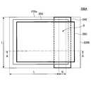
- FIG. 3is a schematic top view of a light emitting element for an illumination device used in Example 1.
- 6is a schematic top view of a light emitting element for a display device used in Example 2.
- FIG. 6is a schematic top view of a light emitting element for a display device used in Example 3.
- FIG. 10is an X-ray diffraction spectrum of samples of Examples 1 to 9.
- 2is a UPS spectrum (work function) in the sample of Example 1.
- 2is a UPS spectrum (ionization potential) in the sample of Example 1.
- 2is a Tauc plot of a film of inorganic material in the sample of Example 1.
- FIG. 10is a diagram collectively showing current-voltage characteristics of the electronic-only device and the samples of Examples 2 to 7.
- FIG. 10is a diagram showing current-voltage-luminance characteristics measured in the organic EL element in Example 10.
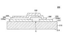
- FIG. 1schematically shows a cross section of a light emitting device 100 (hereinafter referred to as “first light emitting device”) 100 according to an embodiment of the present invention.
- the first light emitting element 100includes a substrate 110, a first electrode 120, an organic layer 150, and a second electrode 180.
- the first electrode 120has a pair of opposing electrode layers (a first bottom electrode layer 120a and a second bottom electrode layer 120b) on the first surface 112 of the substrate 110 that are not in direct contact with each other.
- the resin layer 130is disposed so as to fill the space S between the first bottom electrode layer 120a and the second bottom electrode layer 120b of the first electrode 120 disposed to face each other.
- the organic layer 150includes an electron injection layer, an electron transport layer, an organic light emitting layer, a hole transport layer, a hole injection layer, and the like. However, each layer other than the organic light emitting layer may be omitted if unnecessary.
- the second electrode 180is disposed so as to cover the organic layer 150, and is electrically connected to one bottom electrode layer (for example, the second bottom electrode layer 120b) constituting the first electrode 120.
- the lower surface (second surface) 114 of the substrate 110is a light extraction surface. Therefore, the substrate 110 is a transparent substrate, and the first electrode 120 is a transparent electrode. is there.
- the first light emitting element 100 having such a configurationcan be used in, for example, a lighting device.
- firstWhen operating the first light emitting element 100, first, a voltage is applied between the first bottom electrode layer 120a and the second bottom electrode layer 120b so that the first bottom electrode layer 120a serves as a cathode and the second bottom electrode layer 120b serves as an anode.
- electronsare emitted from the first bottom electrode layer 120a side toward the organic layer 150, and holes are emitted from the second electrode 180 side connected to the second bottom electrode layer 120b toward the organic layer 150. Is done.
- the electrons and holesare recombined in the organic light emitting layer provided in the organic layer 150, and the light emitting material in the organic light emitting layer is excited by the binding energy generated at this time. Light emission occurs when the excited luminescent material returns to the ground state. This light emission is output from the second surface 114 of the substrate 110, thereby making it possible to brighten (“turn on”) an illumination device or the like including the first light emitting element 100.
- the first light emitting device 100further includes a bridge layer 140 disposed on the resin layer 130 so as to cover the resin layer 130.
- the bridge layer 140is electrically connected to each of the two bottom electrode layers 120a and 120b constituting the first electrode 120, and is configured to straddle the space S between the opposing electrodes 120.
- the bridge layer 140is made of a material selected from the group consisting of zinc-tin-silicon-oxygen, zinc-tin-oxygen, and zinc-silicon-oxygen, and has a resistance in the range of 100 k ⁇ to 100 M ⁇ .
- the conventional light emitting devicehas a problem of electrostatic breakdown caused by electrostatic discharge.
- the bridge layer 140is disposed so as to connect the first bottom electrode layer 120a and the second bottom electrode layer 120b.
- the bridge layer 140can function as an appropriate resistance element between the first bottom electrode layer 120a and the second bottom electrode layer 120b. For this reason, during electrostatic discharge, for example, a relatively small current (bypass current) flows from the second bottom electrode layer 120b to the first bottom electrode layer 120a via the bridge layer 140.
- the bridge layer 140is made of the above-described oxide, and is less likely to be damaged by a surge voltage.
- the light emitting device 100it is possible to significantly suppress electrostatic breakdown of the light emitting device due to a large current instantaneously flowing between the bottom electrode layers 120a and 120b during electrostatic discharge. .
- the bridge layer 140is made of an amorphous oxide. Since such an amorphous layer does not have grains and domains, it has a feature that a smooth exposed surface can be formed during the patterning process.
- the organic layer 150is formed on the bridge layer 140 (and the side portion), the coverage of the layer at the interface of the bridge layer 140 / organic layer 150 is improved, and the coverage characteristics of the organic layer 150 can be improved. become.
- the bridge layer 140has a high mobility with respect to carriers such as electrons or holes. For this reason, the bridge layer 140 can supplement a part of the function of the organic layer 150. Specifically, the bridge layer 140 can be used as an electron injection layer, an electron transport layer, a hole injection layer, and / or a hole transport layer. In such an aspect, in the configuration of FIG. 1, the bridge layer 140 may be disposed so as to substantially cover the upper portion of the first bottom electrode layer 120a, for example.
- FIG. 2schematically shows a cross section of another light emitting device (hereinafter referred to as a “second light emitting device”) 200 according to an embodiment of the present invention.
- the second light emitting element 200basically has the same configuration as that of the first light emitting element 100 shown in FIG. Therefore, in the second light emitting device 200 shown in FIG. 2, the same reference numerals as those used in FIG. 1 plus 100 are used for the same components as those in FIG.
- the second light-emitting element 200includes a substrate 210, a first electrode 220 (first bottom electrode layer 220a and second bottom electrode layer 220b), a bridge layer 240, an organic layer 250, a second layer, Electrode 280.
- the second light emitting element 200is different from the first light emitting element 100 in that the resin layer 230 is not provided in the space S between the first bottom electrode layer 220a and the second bottom electrode layer 220b. ing. That is, in the second light emitting element 200, the space S is filled with the bridge layer 240.
- the bridge layer 240is made of a material selected from the group consisting of a zinc-tin-silicon-oxygen system, a zinc-tin-oxygen system, and a zinc-silicon-oxygen system, and ranges from 100 k ⁇ to 100 M ⁇ . It has the characteristic of having the resistance of.
- the bridge layer 240 made of an oxidedoes not have grains and domains, a smooth exposed surface can be formed in the patterning process. For this reason, in the second light emitting device 200, the layer attachment at the interface of the bridge layer 240 / organic layer 250 is improved, and the coverage characteristics of the organic layer 250 can be improved.
- the installation of the resin layer 130 used for filling the space S in the first light emitting element 100can be omitted, and the manufacturing process can be simplified.
- FIG. 3schematically shows a cross section of yet another light emitting device (hereinafter referred to as “third light emitting device”) 300 according to an embodiment of the present invention.
- the third light emitting element 300basically has the same configuration as the second light emitting element 200 shown in FIG. Therefore, in the third light emitting device 300 shown in FIG. 3, the same reference numerals as those in FIG. 2 plus 100 are used for the same components as in FIG.
- the third light-emitting element 300includes a substrate 310, a first electrode 320 (a first bottom electrode layer 320a and a second bottom electrode layer 320b), a bridge layer 340, an organic layer 350, a second Electrode 380.
- the arrangement form of the bridge layer 340is different from that in the second light emitting element 200.
- the bridge layer 340has a high mobility with respect to a carrier such as an electron or a hole, a part of the function of the organic layer 350 can be complemented.
- the bridge layer 340has a function as an electron injection layer, and the first bottom electrode layer 320a is formed on the first bottom surface. It arrange
- the third light-emitting element 300 having such a configurationcan provide the same electrostatic breakdown preventing effect as the first and second light-emitting elements 100 and 200.
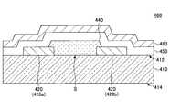
- FIG. 4schematically shows a cross section of a part of a light-emitting element (hereinafter referred to as “fourth light-emitting element”) according to an embodiment of the present invention, which can be used in a display device or the like.
- the fourth light-emitting element 400includes a substrate 410, a first column electrode 420, a bridge layer 440, an organic layer 450, and a second row electrode 480.
- the first column electrode 420has a pair of opposing electrode layers (a first bottom electrode layer 420a and a second bottom electrode layer 420b) on the first surface 412 of the substrate 410.
- the first column electrode 420may be composed of a set of three or more bottom electrode layers that are arranged with a space S therebetween.
- the space Sis filled and arranged with a bridge layer 440.
- the bridge layer 440is electrically connected to each of the two adjacent bottom electrode layers 420a and 420b, and is configured to straddle both bottom electrode layers 420a and 420b.
- the space Smay be filled with a resin layer, and the bridge layer 440 may be disposed so as to cover the resin layer.
- the bridge layer 440is made of a material selected from the group consisting of a zinc-tin-silicon-oxygen system, a zinc-tin-oxygen system, and a zinc-silicon-oxygen system, and has a resistance in the range of 100 k ⁇ to 100 M ⁇ .
- the organic layer 450is disposed on the first column electrode 420 and the bridge layer 440.
- the organic layer 450includes an electron injection layer, an electron transport layer, an organic light emitting layer, a hole transport layer, a hole injection layer, and the like. However, each layer other than the organic light emitting layer may be omitted if unnecessary.
- the second row electrode 480is disposed so as to cover the organic layer 450.
- the second row electrode 480is usually composed of a plurality of upper electrode layers arranged adjacent to each other via a space.
- the lower surface (second surface) 414 of the substrate 410is a light extraction surface. Therefore, the substrate 410 is a transparent substrate, and the first column electrode 420 is a transparent electrode. It is.
- the fourth light emitting element 400 having such a configurationcan be used, for example, for a passive control display device.
- the fourth light emitting element 400includes the bridge layer 440 having the above-described characteristics. For this reason, also in the 4th light emitting element 400, the electrostatic breakdown of the light emitting element which may arise at the time of electrostatic discharge can be suppressed significantly.
- the bridge layer 440 made of an amorphous oxidedoes not have grains and domains, a smooth exposed surface can be formed during the patterning process. For this reason, in the 4th light emitting element 400, the surrounding of a layer in the bridge
- FIG. 5schematically shows a cross section of yet another light emitting device (hereinafter referred to as “fifth light emitting device”) 500 according to an embodiment of the present invention.
- the fifth light emitting element 500has basically the same configuration as the fourth light emitting element 400 shown in FIG. 4. Therefore, in the fifth light emitting device 500 shown in FIG. 5, the same reference numerals as those used in FIG. 5 plus 100 are used for the same components as in FIG.
- the fifth light-emitting element 500includes a substrate 510, a first column electrode 520 (first bottom electrode layer 520a and second bottom electrode layer 520b), a bridge layer 540, an organic layer 550, 2 row electrodes 580.
- the arrangement form of the bridge layer 540is different from that in the fourth light emitting element 400.
- the bridge layer 540has a high mobility with respect to a carrier such as an electron or a hole, a part of the function of the organic layer can be supplemented. Therefore, in the example of the fifth light emitting element 500 shown in FIG. 5, the bridge layer 540 has a function as an electron injection layer, and the bottom electrode layers 520 a and 520 b constituting the first column electrode 520. Is placed on top of these layers so as to cover these layers. With such a configuration, the number of layers constituting the organic layer 550 can be reduced.
- the fifth light-emitting element 500can also provide an electrostatic breakdown preventing effect as in the fourth light-emitting element 400.
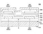
- FIG. 6schematically shows a cross section of yet another light emitting device (hereinafter referred to as “sixth light emitting device”) 600 according to an embodiment of the present invention.
- the sixth light emitting element 600includes a substrate 610, a TFT backplane 630, a first electrode 620, a bridge layer 640, layers 651 to 655 constituting the organic layer, a second Electrode 680.
- the TFT backplane 630is disposed on the first surface 612 of the substrate 610.
- the TFT backplane 630has various semiconductor circuit elements.
- the first electrode 620has a pair of opposing electrode layers (a first bottom electrode layer 620a and a second bottom electrode layer 620b) on the TFT backplane 630. Note that the first electrode 620 may be formed of a set of three or more bottom electrode layers that are disposed with a space S therebetween.
- a bridge layer 640is disposed on the first electrode 620.
- the bridge layer 640has a high mobility with respect to a carrier such as an electron or a hole, a part of the function of the organic layer can be complemented. Therefore, in the example of the sixth light-emitting element 600 illustrated in FIG. 6, the bridge layer 640 has a function as an electron injection layer, and each of the bottom electrode layers 620 a and 620 b that configure the first electrode 620. At the top, it is arranged to cover these layers.
- the bridge layer 640fills the space S.
- the space Smay be filled with a resin layer, and the bridge layer 640 may be disposed so as to cover the resin layer.
- the bridge layer 640is made of a material selected from the group consisting of a zinc-tin-silicon-oxygen system, a zinc-tin-oxygen system, and a zinc-silicon-oxygen system, and has a resistance in the range of 100 k ⁇ to 100 M ⁇ .
- the layers 651 to 655 constituting the organic layerare arranged. More specifically, an electron transport layer 651, an organic light emitting layer 653, and a hole transport layer (or injection layer) 655 are stacked in this order on the bridge layer 640.
- the organic light emitting layer 653is not disposed as a continuous layer but is disposed as a separate layer in a region corresponding to each bottom electrode layer.
- the first organic light emitting layer 653ais disposed in the region corresponding to the bottom electrode layer 620a
- the second organic light emitting layer 653bis disposed in the region corresponding to the bottom electrode layer 620b. Is done.
- the first organic light emitting layer 653a and the second organic light emitting layer 653bmay have different emission colors.
- the second electrode 680is disposed so as to cover the hole transport layer (or injection layer) 655.
- the lower surface (second surface) 614 of the substrate 610is a light extraction surface. Therefore, the substrate 610 is a transparent substrate, and the first electrode 620 is a transparent electrode. is there.
- the sixth light emitting element 600C having such a configurationcan be used for, for example, an active control type display device.
- the sixth light emitting element 600includes the bridge layer 640 having the above-described characteristics. For this reason, also in the 6th light emitting element 600, the electrostatic destruction of the light emitting element which may arise at the time of electrostatic discharge can be suppressed significantly.
- the bridge layer 640 made of an amorphous oxidedoes not have grains and domains, a smooth exposed surface can be formed during the patterning process. For this reason, in the sixth light emitting element 600, the layer attachment at the bridge layer 640 / electron transport layer 651 interface is improved, and the coverage characteristics of the organic layer 450 can be improved.
- the material constituting the substrate 110is not particularly limited, and the substrate 110 may be a glass substrate or a plastic substrate. Note that when the light-emitting element is a bottom emission type and the second surface 114 of the substrate 110 is a light extraction surface, the substrate 110 is a transparent substrate.
- the first electrode 120When the light emitting element is a bottom emission type, the first electrode 120 is a transparent electrode. In that case, the first electrode 120 may be ITO, tin oxide, or the like.
- the first electrode 120may be a metal electrode such as an aluminum alloy.
- the resin layer 130may be made of any resin material as long as the space S can be filled appropriately.
- the resin layer 130may be, for example, a polyimide resin or an acrylic resin.
- the bridge layer 140is an oxide and is made of a material selected from the group consisting of a zinc-tin-silicon-oxygen system, a zinc-tin-oxygen system, and a zinc-silicon-oxygen system.
- the bridge layer 140may be a zinc-tin-germanium-oxygen system.
- the bridge layer 140may be amorphous, microcrystalline, or a mixture of amorphous and microcrystalline.
- the bridge layer 140When the bridge layer 140 is composed of a zinc-silicon-oxygen-based material, the bridge layer 140 contains zinc (Zn), silicon (Si), and oxygen (O), and the atomic ratio of Zn / (Zn + Si) is 0. It is preferably 30 to 0.95. This is because, when the atomic ratio of Zn / (Zn + Si) is 0.30 or more and 0.95 or less, the above-described resistance is easily obtained, and a layer with high flatness is easily obtained.
- the bridge layer 140may be an indium-silicon-oxygen-based, indium-gallium-zinc-oxygen-based, indium-zinc-oxygen-based, or germanium-zinc-oxygen-based material.
- the atomic ratio of Zn / (Zn + Si)is more preferably 0.6 or more, and further preferably 0.7 or more.
- the atomic ratio of Zn / (Zn + Si)is more preferably 0.92 or less, and further preferably 0.90 or less.
- the bridge layer 140When the bridge layer 140 is composed of a zinc-tin-silicon-oxygen-based material, the bridge layer 140 contains zinc (Zn), tin (Sn), silicon (Si), and oxygen (O), and is converted into an oxide.
- SnO 2is preferably more than 15 mol% and 95 mol% or less with respect to 100 mol% in total of the oxides of the bridge layer 140. This is because if the SnO 2 content exceeds 15 mol% and 95 mol% or less, the bridge layer 140 with high flatness can be easily obtained, and the above-described resistance can be easily obtained.
- SnO 2is more preferably 60 mol% or more, and further preferably 70 mol% or more.
- SnO 2is more preferably 90 mol% or less, and still more preferably 80 mol% or less.
- the bridge layer 140is more preferably 7 mol% or more and 30 mol% or less of SiO 2 with respect to 100 mol% in total of the oxides of the bridge layer 140 in terms of oxide. This is because if the SiO 2 content is 7 mol% or more and 30 mol% or less, the electron affinity is not too high, the volume resistivity is not too high, and the above-described resistance is easily obtained.
- SiO 2is more preferably 10 mol% or more, and further preferably 20 mol% or more. SiO 2 is more preferably at most 40 mol%, further preferably at most 30 mol%.
- the bridge layer 140When the bridge layer 140 is made of a zinc-tin-oxygen-based material, the bridge layer 140 contains zinc (Zn), tin (Sn), and oxygen (O), and the oxide of the bridge layer 140 in terms of oxides. against a total of 100 mol%, SnO 2 is 15 mol% greater, preferably at most 95 mol%.
- SnO 2is more than 15 mol% and 95 mol% or less, it is easy to obtain a bridge layer 140 with high flatness, and it is easy to maintain the state of amorphous, microcrystal, or a thin film in which amorphous and microcrystal are mixed, This is because the above-described resistance can be easily obtained, an oxide target for film formation can be easily obtained, and a thin film can be easily formed.
- SnO 2is more preferably at least 30 mol%, further preferably at least 40 mol%. SnO 2 is more preferably 65 mol% or less, and even more preferably 55 mol% or less.
- the bridge layer 140has a resistance in the range of 100 k ⁇ to 100 M ⁇ .
- the resistance of the bridge layer 140is more preferably 200 k ⁇ or more, further preferably 500 k ⁇ or more, and particularly preferably 1 M ⁇ or more.
- the resistance of the bridge layer 140is more preferably 50 M ⁇ or less, further preferably 20 M ⁇ or less, and particularly preferably 10 M ⁇ or less.
- the bridge layer 140may have a specific resistance of a film formed of 500 ⁇ cm to 500 k ⁇ cm.
- a film having an electron density of 10 16 cm ⁇ 1 and a mobility of 0.13 cm 2 / Vsmay be used.
- a film having a specific resistance of about 500 k ⁇ cma film having an electron density of 10 17 cm ⁇ 1 and a mobility of 1.25 ⁇ 10 ⁇ 4 cm 2 / Vs may be used.
- the specific resistance of the film formed by the bridge layer 140is more preferably 800 ⁇ cm or more, and further preferably 1 k ⁇ cm or more.
- the specific resistance of the film formed by the bridge layer 140is more preferably 300 k ⁇ cm or less, and even more preferably 100 k ⁇ cm or less.
- the physical parameters such as the electrical resistance and mobility of the bridge layer 140can be adjusted to some extent by changing the material composition.
- the bridge layer 140can be used in place of the electron injection layer, the electron transport layer, the organic light emitting layer, the hole transport layer, and the hole injection layer in the organic layer 150 as necessary.
- the bridge layer 140 made of such an amorphous oxidecan be formed by a film forming technique such as a sputtering method and a PVD method.
- the bridge layer 140is more easily flat when the amorphous or amorphous state is dominant.
- the relationship between the electron affinity and the compositiontends to be linear, so that the power supplied to the layer can be easily controlled.
- the bridge layeris more easily obtained when the amorphous or amorphous state is dominant. Since the bridge layer is more easily oriented in the layer thickness direction than the amorphous layer, the bridge layer is more likely to improve the electronic characteristics in the layer thickness direction when the crystallite is dominant.
- the resin layer 130may be omitted.
- the space Sis filled with the bridge layer 240 (see, for example, FIG. 2).
- the bridge layer 240can be sufficiently thicker than the first electrode 120 so that the step of the first electrode 120 can be sufficiently covered.
- the short circuit between the first electrode 120 and the second electrode 280can be suppressed.
- the bridge layermay be thicker than the first electrode, and the bridge layer may be 1.5 or more times thicker than the first electrode.
- the film thickness of the layermay be twice or more the film thickness of the first electrode.
- the thickness of the bridge layeris preferably 100 nm or more, more preferably 200 nm or more, and particularly preferably 300 nm or more.
- the organic layer 150includes an electron injection layer, an electron transport layer, an organic light emitting layer, a hole transport layer, a hole injection layer, and the like. Conventionally known layers can be used for these layers.
- one or more layers other than the organic light emitting layermay be omitted.
- the bridge layer 140when used as an electron injection layer or a hole injection layer, the electron injection layer and the hole injection layer in the organic layer 150 can be omitted.
- the second electrode 180may be a metal electrode such as an aluminum alloy.
- the second electrode 180is a transparent electrode, and may be made of, for example, ITO and tin oxide.
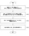
- FIG. 7schematically shows a flow of a method for manufacturing a light-emitting element according to an embodiment of the present invention (hereinafter referred to as “first manufacturing method”).
- the first manufacturing methodis: Forming a pair of opposing electrode layers on the substrate as a first electrode (step S110); Placing a bridge layer in electrical contact with each of the pair of electrode layers and connecting each of the first electrodes (step S120); Forming an organic layer on at least one of the pair of electrode layers (step S130); Disposing a second electrode on the organic layer (step S140); Have
- Step S110First, the substrate 210 is prepared.
- the substrateis a transparent substrate.
- the first electrode 220is formed on the substrate.
- the first electrode 220is a transparent electrode.
- the first electrode 220is patterned so as to have at least a pair of electrode layers 220a and 220b.
- Step S120Next, the bridge layer 240 is formed so as to come into contact with and connect the electrode layers 220a and 220b.
- the bridge layer 240may be formed, for example, by forming it as an entire film by a film forming technique such as sputtering, and then patterning the film by, for example, an etching process.
- a film forming techniquesuch as sputtering
- the bridge layer 240is made of an oxide and has no grains and domains. Therefore, a smooth exposed surface can be formed after the patterning process of the bridge layer 240. Such a smooth exposed surface makes it possible to properly form each layer in the processes after step S130. In order to obtain a smooth exposed surface, it is advantageous that the oxide is amorphous.
- the bridge layer 240functions as an appropriate resistance element between the pair of electrode layers 220a and 220b in the subsequent steps. Therefore, in the first manufacturing method, electrostatic breakdown due to electrostatic discharge can be significantly avoided even during the manufacturing of the light emitting element.
- the organic layer 250is formed on at least one of the pair of electrode layer layers 220a and 220b.
- the organic layer 250may be in contact with at least a part of the bridge layer 240.
- the exposed surface of the bridge layer 240is a relatively smooth surface. For this reason, at the interface of the bridge layer 240 / organic layer 250, the coverage of the organic layer 250 is improved, and the coverage characteristics of the organic layer 150 can be improved.
- the organic layer 250includes a plurality of layers including an organic light emitting layer.
- the bridge layer 240can be disposed so as to cover the electrode layer 220a and function as an electron injection layer (see FIG. 3).
- one or more layers constituting the organic layer 250, such as an electron injection layer,can be omitted.
- the second electrode 280is disposed on the organic layer 250.
- the second electrode 280may be made of metal.
- the second electrode 280is electrically connected to at least one of the pair of electrode layers 220a and 220b (for example, the electrode layer 220b). This makes it possible to apply voltages having opposite polarities to the pair of electrode layers 220a and 220b.
- the second light emitting element 200 as shown in FIG. 2can be manufactured.
- Example IUsing the configuration of the second light emitting element 200 shown in FIG. 2 as an example, it was verified whether the light emitting element according to the embodiment of the present invention can actually be used as a light emitting element for a lighting device.
- the AA cross section of the light emitting element 200A in FIG. 8schematically corresponds to the configuration shown in FIG. In FIG. 8, the substrate is omitted.
- the light emitting element 200Ahas a light emitting portion having a square shape with a vertical L and a horizontal L, and the space S between the first bottom electrode layer 220a and the second bottom electrode layer 220b has a width.
- GL was 100 mm and G was 200 ⁇ m.
- the characteristics relating to the bridge layer 240were actually measured from an oxide film formed on a glass substrate by a sputtering method.
- a sputtering target having a composition of 90 mol% ZnO-10 mol% SiO 2was used.
- the film formation conditionswere as follows: Deposition pressure: 0.3 Pa Gas composition; Ar + 10% O 2 Target-substrate distance: 6.5 cm Deposition energy density: 9.9 W / cm 2
- the current value I 1 flowing through the bridge layer 240was sufficiently smaller than the current value i 1 flowing through the light emitting element 200A (about 0.002%). From this, it was confirmed that the installation of the bridge layer 240 has almost no influence on the deterioration of the characteristics of the light emitting element, and the light emitting element 200A can be sufficiently used as a light emitting element for a lighting device.
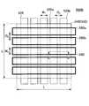
- Example IIUsing the configuration of the fifth light emitting element 500 shown in FIG. 5 as an example, it was verified whether the light emitting element according to an embodiment of the present invention can actually be used as a light emitting element for a passive control display device. .
- the BB cross section in FIG. 9 of the light emitting element 500Broughly corresponds to the configuration shown in FIG. In FIG. 9, the substrate is omitted.
- the first electrode 520is a column electrode
- the second electrode 580is a row electrode.
- One intersection region of one of the column electrodes and one of the row electrodesis a light emitting portion.
- Each bottom electrode layers 520a constituting the first electrode 520, the width of 520bis W 1, the gap therebetween is G 1.
- the upper electrode layer 580a constituting the second electrode 580, the width of 580bis W 2, the gap therebetween is G 2.
- the area S of one light emitting portionis a value obtained by multiplying W 1 by W 2 .
- W 1 and W 2are both 270 ⁇ m
- G 1 and G 2are both 30 ⁇ m.
- the bridge layer 540 and the organic layer 550have the same shape in a top view, and both are formed in a square shape with one side length L.
- Lwas 20 mm.
- the characteristics relating to the bridge layer 540were actually measured from an oxide film formed on a glass substrate by a sputtering method.
- a sputtering target having a composition of 85 mol% ZnO-15 mol% SiO 2was used.
- the film formation conditionswere as follows: Deposition pressure: 0.25 Pa Gas composition; Ar Target-substrate distance: 10 cm Deposition energy density: 9.9 W / cm 2
- the light emitting area Sis a value obtained by multiplying W 1 by W 2 , W 1 is 270 ⁇ m, W 2 is 270 ⁇ m, and the area S is 7.29 ⁇ 10 ⁇ 8 m 2 .
- Example IIIUsing the configuration of the sixth light emitting element 600 shown in FIG. 6 as an example, it was verified whether the light emitting element according to the embodiment of the present invention can actually be used as a light emitting element for an active control display device. .
- each memberhas a dimensional relationship as shown in the top view 10 is assumed.
- the CC cross section in FIG. 10 of the light emitting element 600Croughly corresponds to the configuration shown in FIG.
- only the TFT backplane 630 and the first electrode 620 (bottom electrode layers 620a and 620b)are shown in FIG. 10 for clarity.
- the dimension and the formation position of the bridge layer 640substantially coincide with the dimension and the formation position of the TFT backplane 630 when viewed from above. Furthermore, when viewed from the top, the dimensions and formation positions of the bottom electrode layers 620a and 620b constituting the first electrode 620 are assumed to match the dimensions and formation positions of the corresponding organic light emitting layers 653a and 653b.
- W 1was 70 ⁇ m
- W 2was 260 ⁇ m
- G 1was 30 ⁇ m
- G 2was 40 ⁇ m.
- the characteristics relating to the bridge layer 640were actually measured from an oxide film formed on a glass substrate by a sputtering method.
- a sputtering target having a composition of 90 mol% ZnO-10 mol% SiO 2was used.
- the light emission area Swas obtained by multiplying W 1 by W 2 , W 1 was 260 ⁇ m, W 2 was 70 ⁇ m, and the light emission area S was 1.82 ⁇ 10 ⁇ 8 m 2 .
- the luminance of the light-emitting element 600Cis set to 2000 cd / m 2 .
- Example 1Samples in which oxide films were formed on various deposition substrates were manufactured by the following method.
- the film formation substratea nickel substrate, a glass substrate, or the like was used.
- RF magnetron sputtering apparatusmanufactured by ULVAC
- sputtering targeta sintered body target having a diameter of 2 inches and containing ZnO and SiO 2 at a predetermined ratio was used.
- the deposition target substratewas introduced into the chamber of the sputtering apparatus.
- a predetermined sputtering gasAs a sputtering gas, argon (Ar) gas (G1 grade: purity 99.99995 vol.%) Or a mixed gas of oxygen (O 2 ) gas (G1 grade: purity 99.99995 vol.%) And Ar gas (G1 grade) It was used. That is, Ar gas or an O 2 / Ar mixed gas having an oxygen concentration of 20% was used as the sputtering gas.
- the sputtering gas pressurewas set to a predetermined pressure
- the distance between the target and the deposition target substrate (TS distance)was set to a predetermined distance
- power of 50 Wwas applied to the cathode of the sputtering apparatus.
- the substrate temperature during film formationwas 70 ° C. or lower.
- Example 2 to Example 9Samples in which oxide films were formed on various deposition substrates were prepared in the same manner as in Example 1 (Examples 2 to 9). However, in Examples 2 to 9, film forming conditions different from those in Example 1 were adopted.
- Table 1summarizes the film forming conditions used in Examples 1 to 9.
- the atomic ratiowas determined by SEM-EDX analysis of the oxide film.
- the acceleration voltagewas set to 10 kV.
- the X-ray diffraction spectrumwas measured by the Zeeman Borin method using an Rigaku X-ray diffractometer RINT-2000. Details of the Zeemanborin method are shown in the Japan Institute of Metals, Vol. 27, No. 6, pages 461-465 (1988).
- An electron beamwas irradiated onto Cu under the conditions of an acceleration voltage of 50 kV and a discharge current of 300 mA, the generated CuK ⁇ ray was fixed at an incident angle of 0.5 °, and the sample was irradiated to obtain a diffraction pattern.
- FIG. 11shows the diffraction pattern obtained for each sample.
- the films obtained in Examples 1 to 7all have a Scherrer diameter of 5 nm or less, and no sharp peak is observed in X-ray diffraction, confirming that the amorphous or amorphous state is dominant. It was. On the other hand, in Examples 8 and 9, the Scherrer diameter was larger than 5 nm, and it was confirmed that the crystal quality was dominant in X-ray diffraction.
- the deposition target substratewas a substrate in which 150 nm of ITO was deposited on an alkali-free glass substrate (hereinafter referred to as an ITO substrate).
- the oxide film(thickness 10 nm) was formed on the surface of the ITO substrate on which ITO was formed.
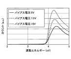
- Ultraviolet photoelectron spectroscopywas carried out by irradiating the film with ultraviolet light (He (I), 21.22 eV) from a He lamp in a high vacuum of 10 ⁇ 7 Pa or higher.
- FIG. 12is a diagram showing the relationship between the photoelectron count number and the photoelectron kinetic energy
- FIG. 13is a diagram showing the relationship between the photoelectron count number and the binding energy.
- the work function of the thin film in the sample of Example 1was calculated to be 3.9 eV. Further, from FIG. 13, the ionization potential of the oxide film in the sample of Example 1 obtained by the sum of the binding energy and the work function was calculated to be 6.6 eV.
- the light absorption coefficientwas calculated by measuring the reflectance and transmittance using each sample. Moreover, the optical band gap was calculated
- FIGS. 14 and 15show Tauc plots of the oxide films in Examples 1 and 2, respectively.
- the electron affinity of the oxide film in the sample of Example 1is expected to be 2.6 eV when compared with the result of the ionization potential obtained by the UPS measurement described above. Also in the oxide films in the samples of Examples 2 to 7, assuming the same ionization potential, the electron affinity is expected to be about 3.3 to 3.4 eV.
- a 2 mol% Nd-containing aluminum (product name: AD20) target manufactured by Kobelco Research Institute with a diameter of 2 incheswas used.
- the electron-only devicehas a cathode as a bottom electrode on a glass substrate, an electron transport layer having a thickness of 150 nm on the bottom electrode, and an anode as a top electrode on the electron transport layer so as to be orthogonal to the bottom electrode. Arranged and configured.
- the cathodewas formed by sputtering film formation using Nd-containing aluminum having a thickness of 80 nm and a width of 1 mm using a 2 mol% Nd-containing aluminum target (product name: AD20) manufactured by Kobelco Research Institute. A 150 nm thick Alq3 layer was formed as the electron transport layer. The anode was formed by vacuum vapor deposition of aluminum so as to have a thickness of 80 nm.
- a voltagewas applied to the cathode and anode of the electronic only element, and the current value generated at this time was measured.
- FIG. 16shows current-voltage characteristics (denoted as “Alq3”) obtained in the electronic-only device.
- I / AE / ( ⁇ ⁇ L) Formula (1)
- Iis the current density
- Ais the area
- Eis the voltage
- ⁇is the resistivity
- Lis the thickness of the electron transport layer.
- the thickness of the electron transport layerwas 150 nm.
- FIG. 16shows that when the oxide film in the samples of Examples 2 to 7 is used for the electron transport layer, it has sufficient electron transport properties as an organic EL device even when the thickness is 150 nm.
- the organic EL elementwas produced by the following method and its characteristics were evaluated.
- An organic EL devicehas a cathode as a bottom electrode on a glass substrate, and an electron transport layer, a light emitting layer, a hole transport layer, a hole injection layer, and an anode as a top electrode are disposed on the cathode in order, and light is emitted from the anode side. It was set as the structure which takes out. In Example 11, the formation of the electron injection layer, the hole block layer, and the electron block layer was omitted.
- a cathodewas formed on a glass substrate.
- An alkali-free glass substratewas used as the glass substrate.
- the cleaned glass substrate and metal maskwere placed in the chamber of the sputtering apparatus.
- a target for cathode film formationwas placed in the chamber of the sputtering apparatus.
- an aluminum (product name: AD20) target of 2 mol% Nd containing 2 inches in diameter manufactured by Kobelco Research Institutewas used.
- a cathode 120was formed by sputtering on a glass substrate so as to have a thickness of 80 nm and a width of 1 mm.
- the sputtering gaswas Ar
- the sputtering gas pressurewas 0.3 Pa
- a power of 50 Wwas applied to the sputtering cathode.
- an electron transport layerwas formed on the cathode. Without moving the metal mask, an oxide film having a thickness of 100 nm was formed as an electron transport layer on the glass substrate on which the cathode was formed under the sputtering conditions in Example 7.
- a light emitting layer, a hole transport layer, and a hole injection layerwere formed on the electron transport layer.
- the glass substrate on which the electron transport layer (and the cathode) was formedwas transported from the sputtering apparatus chamber to the vacuum deposition chamber in a high vacuum atmosphere of 10 ⁇ 4 Pa or less.
- Alq3was deposited as a light emitting layer on the electron transport layer to a thickness of 50 nm.
- ⁇ -NPDwas deposited as a hole transport layer on the light emitting layer to a thickness of 50 nm.
- MoO xwas deposited to a thickness of 0.8 nm as a hole injection layer on the hole transport layer.
- an anodewas formed on the hole injection layer.
- goldwas deposited as an anode with a thickness of 10 nm and a width of 1 mm.
- the degree of vacuum at the time of vapor depositionwas about 8 ⁇ 10 ⁇ 6 Pa. Since the anode transmits visible light, light is extracted from the anode (top electrode) side.
- the light emitting layer, the hole transport layer, and the hole injection layerwere formed using a metal mask so as to completely cover the cathode and the electron transport layer.
- the anodewas formed using a metal mask so as to be orthogonal to the cathode.
- the overlapping 1 mm ⁇ 1 mm region of the 1 mm wide anode deposited so as to be orthogonal to the 1 mm wide cathodeis the region that emits light when voltage is applied.
- An organic EL element including an injection layer and an anode made of goldwas produced.
- FIG. 17shows the obtained current-voltage-luminance characteristics.
- the luminance and current density of the organic EL elementincreased from 8 V, and the luminance was 1500 cd / m 2 and the current density was 2.6 A / cm 2 at 12 V. From this result, it was confirmed that the oxide film having a thickness of 100 nm functions as an electron transporting layer.
- the oxide layercan be used both as a bridge layer and an electron transport layer. In this case, it is possible to simultaneously form the bridge layer and the electron transport layer without increasing the number of film forming steps.
- the present inventioncan be used for, for example, a lighting device and a display device.
Landscapes
- Physics & Mathematics (AREA)
- Optics & Photonics (AREA)
- Engineering & Computer Science (AREA)
- Microelectronics & Electronic Packaging (AREA)
- Manufacturing & Machinery (AREA)
- Electroluminescent Light Sources (AREA)
- Illuminated Signs And Luminous Advertising (AREA)
Abstract
Description
Translated fromJapanese本発明は、発光素子、表示装置および照明装置に関する。The present invention relates to a light emitting element, a display device, and a lighting device.
有機EL(有機エレクトロルミネッセンス)素子のような発光素子は、ディスプレイ(表示装置)、バックライト、および照明装置等に広く用いられている。Light-emitting elements such as organic EL (organic electroluminescence) elements are widely used in displays (display devices), backlights, lighting devices, and the like.
一般的な発光素子は、基板上に設置された第1の電極と、第2の電極と、これらの電極間に設置された発光層とを有する。両電極間に電圧を印加すると、それぞれの電極から、発光層にホールおよび電子が注入される。このホールと電子が発光層内で再結合された際に、結合エネルギーが生じ、この結合エネルギーによって発光層中の発光材料が励起される。励起した発光材料が基底状態に戻る際に発光が生じるため、これを利用することにより、光を外部に取り出すことができる。A general light emitting element has a first electrode disposed on a substrate, a second electrode, and a light emitting layer disposed between these electrodes. When a voltage is applied between both electrodes, holes and electrons are injected from each electrode into the light emitting layer. When the holes and electrons are recombined in the light emitting layer, binding energy is generated, and the light emitting material in the light emitting layer is excited by this binding energy. Since light is emitted when the excited light emitting material returns to the ground state, light can be extracted to the outside by using this.
このような発光素子において、素子の帯電防止のため、基板の裏面に帯電防止膜を形成することが開示されている(特許文献1)。In such a light emitting element, it is disclosed that an antistatic film is formed on the back surface of the substrate in order to prevent the element from being charged (Patent Document 1).
発光素子の中には、使用材料が環境中の酸素や水分などの影響を受けやすく、これにより性能が劣化するものがある。また、このような発光素子の場合、性能低下を抑制するため、酸素および水分を制御した環境下で、発光素子が製造されまたは使用される。Some light-emitting elements are susceptible to the influence of oxygen, moisture, etc. in the environment, resulting in performance degradation. In the case of such a light-emitting element, the light-emitting element is manufactured or used in an environment in which oxygen and moisture are controlled in order to suppress performance degradation.
しかしながら、このような環境下では、発光素子が静電気による帯電を受けやすく、この静電気が放電した際に、構成素子が静電破壊されるおそれがある。このため、発光素子の分野では、静電気対策が重要な一課題となっている。However, in such an environment, the light emitting element is easily charged by static electricity, and when the static electricity is discharged, the constituent elements may be electrostatically destroyed. For this reason, countermeasures against static electricity are an important issue in the field of light emitting devices.
ここで、前述のように、特許文献1には、有機エレクトロルミネッセンス素子の静電気対策のため、素子を構成する基板の裏面等に、帯電防止膜を形成することが示されている。Here, as described above,
しかしながら、静電気による帯電および放電は、必ずしも、基板の裏面側で生じるとは限られない。特に、発光素子の製造中は、基板の上部、すなわち構成素子側から、静電気の放電による静電破壊が生じるおそれがある。特許文献1のような静電気対策では、このような、基板の裏面以外の場所での静電気の放電による静電破壊を十分に抑制することは難しい。However, charging and discharging due to static electricity does not necessarily occur on the back side of the substrate. In particular, during the manufacture of the light emitting element, there is a possibility that electrostatic breakdown due to electrostatic discharge may occur from the upper part of the substrate, that is, the component element side. In the countermeasure against static electricity as in
また、基板の裏面に帯電防止膜を形成した場合、発光素子のハンドリングおよび搬送などの際に、帯電防止膜が擦れて基板から剥離するおそれがある。帯電防止膜が剥離した場合、もはや帯電防止効果は得られなくなってしまう。また、製造過程においてそのような剥離が生じると、剥離物がコンタミネーションの原因となってしまう。In addition, when an antistatic film is formed on the back surface of the substrate, the antistatic film may be rubbed and peeled off from the substrate when the light emitting element is handled or transported. When the antistatic film is peeled off, the antistatic effect can no longer be obtained. Moreover, when such peeling occurs in the manufacturing process, the peeled material causes contamination.
このように、発光素子の静電破壊の問題に関しては、未だ十分な対策が確立されているとは言い難く、今もなお有効な対策が要望されている。As described above, it is difficult to say that sufficient countermeasures have been established for the problem of electrostatic breakdown of light emitting elements, and effective countermeasures are still desired.
本発明は、このような背景に鑑みなされたものであり、本発明では、製造過程および使用状態のいずれにおいても、静電破壊を有意に抑制できる発光素子を提供することを目的とする。また、本発明では、そのような発光素子を有する表示装置および照明装置を提供することを目的とする。The present invention has been made in view of such a background, and an object of the present invention is to provide a light-emitting element capable of significantly suppressing electrostatic breakdown in both the manufacturing process and the use state. It is another object of the present invention to provide a display device and a lighting device having such a light emitting element.
本発明では、発光素子であって、
基板の第1の表面に、相互に離間して対向するように配置された一対の第1の電極と、
前記第1の電極の少なくとも一つの上に配置された発光層と、
前記発光層の上に配置された第2の電極と、
前記第1の電極のそれぞれをつなぐブリッジ層と、
を有し、
前記ブリッジ層は、100kΩ~100MΩの範囲の抵抗を有する材料で構成される、発光素子が提供される。In the present invention, a light emitting device,
A pair of first electrodes disposed on the first surface of the substrate so as to face each other at a distance from each other;
A light emitting layer disposed on at least one of the first electrodes;
A second electrode disposed on the light emitting layer;
A bridge layer connecting each of the first electrodes;
Have
A light emitting device is provided in which the bridge layer is made of a material having a resistance in a range of 100 kΩ to 100 MΩ.
また、本発明では、そのような発光素子を有する表示装置および照明装置が提供される。In the present invention, a display device and a lighting device having such a light emitting element are provided.
本発明では、製造過程および使用状態のいずれにおいても、静電破壊を有意に抑制できる発光素子を提供することが可能となる。また、本発明では、そのような発光素子を有する表示装置および照明装置を提供することが可能となる。In the present invention, it is possible to provide a light emitting element capable of significantly suppressing electrostatic breakdown in both the manufacturing process and the use state. In addition, according to the present invention, it is possible to provide a display device and a lighting device having such a light emitting element.
以下、図面を参照して、本発明の一実施形態について説明する。Hereinafter, an embodiment of the present invention will be described with reference to the drawings.
(本発明の一実施形態による発光素子)
図1には、本発明の一実施形態による発光素子(以下、「第1の発光素子」と称する)100の断面を概略的に示す。(Light Emitting Element According to One Embodiment of the Present Invention)
FIG. 1 schematically shows a cross section of a light emitting device 100 (hereinafter referred to as “first light emitting device”) 100 according to an embodiment of the present invention.
図1に示すように、第1の発光素子100は、基板110と、第1の電極120と、有機層150と、第2の電極180とを有する。As shown in FIG. 1, the first
第1の電極120は、基板110の第1の表面112に、対向する一対の相互に直接接触しない電極層(第1の底面電極層120aおよび第2の底面電極層120b)を有する。対向して配置される第1の電極120の第1の底面電極層120aと第2の底面電極層120bの間の空間Sを充填するように、樹脂層130が配置される。The
有機層150は、電子注入層、電子輸送層、有機発光層、ホール輸送層、およびホール注入層などで構成される。ただし、有機発光層以外の各層は不要な場合、省略しても良い。The
第2の電極180は、有機層150を覆うように配置され、第1の電極120を構成する一つの底面電極層(例えば第2の底面電極層120b)と電気的に接続される。The
なお、図1の例では、基板110の下側表面(第2の表面)114が光取り出し面となっており、従って、基板110は透明基板であり、第1の電極120は、透明電極である。In the example of FIG. 1, the lower surface (second surface) 114 of the
このような構成の第1の発光素子100は、例えば、照明装置などに使用することができる。The first
第1の発光素子100を作動させる場合、まず、第1の底面電極層120aが陰極となり、第2の底面電極層120bが陽極となるように、両者の間に電圧が印加される。これにより、第1の底面電極層120a側から有機層150に向かって電子が放出され、第2の底面電極層120bに接続された第2の電極180側から有機層150に向かってホールが放出される。電子およびホールは、有機層150内に設けられた有機発光層で再結合され、この際に生じた結合エネルギーによって有機発光層中の発光材料が励起される。励起した発光材料が基底状態に戻る際に発光が生じる。この発光は、基板110の第2の表面114から出力され、これにより第1の発光素子100を備える照明装置等を明るく(「オン」に)することができる。When operating the first
ここで、図1に示すように、第1の発光素子100は、さらに、樹脂層130の上に、該樹脂層130を覆うように配置されたブリッジ層140を有する。ブリッジ層140は、第1の電極120を構成する2つの底面電極層120a、120bのそれぞれと電気的に接続され、対向する電極120の間の空間Sを跨ぐように構成される。Here, as shown in FIG. 1, the first
ブリッジ層140は、亜鉛-錫-ケイ素-酸素系、亜鉛-錫-酸素系、および亜鉛-ケイ素-酸素系からなる群から選定された材料で構成され、100kΩ~100MΩの範囲の抵抗を有する。The
前述のように、従来の発光素子では、静電気の放電によって生じる静電破壊が問題となっている。As described above, the conventional light emitting device has a problem of electrostatic breakdown caused by electrostatic discharge.
しかしながら、第1の発光素子100では、第1の底面電極層120aおよび第2の底面電極層120bをつなぐように、ブリッジ層140が配置されている。このような構成では、ブリッジ層140が第1の底面電極層120aと第2の底面電極層120b間の適正な抵抗素子として機能することができる。このため、静電気の放電の際には、例えば、第2の底面電極層120bから第1の底面電極層120aに、ブリッジ層140を介して比較的小さな電流(迂回電流)が流れるようになる。However, in the first
また、ブリッジ層140は、前述の酸化物で構成されており、サージ電圧によって自身が破損する可能性も少ない。Further, the
従って、発光素子100では、静電気の放電の際に、両底面電極層120aおよび120b間に瞬間的に大電流が流れて、発光素子が静電破壊することを有意に抑制することが可能となる。Therefore, in the
さらに、ブリッジ層140は、非晶質の酸化物で構成される。このような非晶質の層は、グレインおよびドメインを有しないため、パターン化処理の際に、平滑な露出表面を形成することができるという特徴を有する。Furthermore, the
このため、ブリッジ層140の上(および側部)に有機層150を形成した場合、ブリッジ層140/有機層150界面における層の付き周りが良くなり、有機層150のカバレージ特性を高めることが可能になる。For this reason, when the
なお、ブリッジ層140は、電子またはホールのような担体に対して、高い移動度を有する。このため、ブリッジ層140は、有機層150の機能の一部を補完することができる。具体的には、ブリッジ層140は、電子注入層、電子輸送層、ホール注入層、および/またはホール輸送層として使用することができる。このような態様では、図1の構成において、ブリッジ層140は、例えば、第1の底面電極層120aの上部をほぼ覆うように配置されても良い。The
(本発明の一実施形態による別の発光素子)
次に、図2を参照して、本発明の一実施形態による別の発光素子について説明する。図2には、本発明の一実施形態による別の発光素子(以下、「第2の発光素子」と称する)200の断面を概略的に示す。(Another light emitting device according to an embodiment of the present invention)
Next, another light emitting device according to an embodiment of the present invention will be described with reference to FIG. FIG. 2 schematically shows a cross section of another light emitting device (hereinafter referred to as a “second light emitting device”) 200 according to an embodiment of the present invention.
図2に示すように、第2の発光素子200は、基本的に、図1に示した第1の発光素子100とほぼ同様の構成を有する。従って、図2に示した第2の発光素子200において、図1と同様の構成部材には、図1で使用した参照符号に100を加えた参照符号が使用されている。例えば、第2の発光素子200は、基板210と、第1の電極220(第1の底面電極層220aおよび第2の底面電極層220b)と、ブリッジ層240と、有機層250と、第2の電極280とを有する。As shown in FIG. 2, the second
ただし、第2の発光素子200は、第1の底面電極層220aと第2の底面電極層220bの間の空間Sに、樹脂層230を有しない点で、第1の発光素子100とは異なっている。すなわち、第2の発光素子200において、空間Sには、ブリッジ層240が充填される。However, the second
前述のように、ブリッジ層240は、亜鉛-錫-ケイ素-酸素系、亜鉛-錫-酸素系、および亜鉛-ケイ素-酸素系からなる群から選定された材料で構成され、100kΩ~100MΩの範囲の抵抗を有するという特徴を有する。As described above, the
従って、第2の発光素子200においても、ブリッジ層240の存在により、静電気の放電の際に、両底面電極層220aおよび220b間に瞬間的に大電流が流れて、発光素子が静電破壊するという問題を有意に抑制できる。Accordingly, also in the second
また、酸化物で構成されるブリッジ層240は、グレインおよびドメインを有しないため、パターン化処理の際に、平滑な露出表面を形成することができる。このため、第2の発光素子200では、ブリッジ層240/有機層250界面における層の付き周りが良くなり、有機層250のカバレージ特性を高めることが可能になる。Further, since the
さらに、第2の発光素子200では、第1の発光素子100において、空間Sの充填に使用されている樹脂層130の設置を省略することができ、製造プロセスの簡略化が可能となる。Furthermore, in the second
(本発明の一実施形態によるさらに別の発光素子)
次に、図3を参照して、本発明の一実施形態によるさらに別の発光素子について説明する。図3には、本発明の一実施形態によるさらに別の発光素子(以下、「第3の発光素子」と称する)300の断面を概略的に示す。(Still another light emitting device according to an embodiment of the present invention)
Next, still another light emitting device according to an embodiment of the present invention will be described with reference to FIG. FIG. 3 schematically shows a cross section of yet another light emitting device (hereinafter referred to as “third light emitting device”) 300 according to an embodiment of the present invention.
図3に示すように、第3の発光素子300は、基本的に、図2に示した第2の発光素子200とほぼ同様の構成を有する。従って、図3に示した第3の発光素子300において、図2と同様の構成部材には、図2で使用した参照符号に100を加えた参照符号が使用されている。例えば、第3の発光素子300は、基板310と、第1の電極320(第1の底面電極層320aおよび第2の底面電極層320b)と、ブリッジ層340と、有機層350と、第2の電極380とを有する。As shown in FIG. 3, the third
ただし、第3の発光素子300では、ブリッジ層340の配置形態が第2の発光素子200の場合とは異なっている。However, in the third
前述のように、ブリッジ層340は、電子またはホールのような担体に対して、高い移動度を有するため、有機層350の機能の一部を補完することができる。例えば、図3に示した第3の発光素子300の例では、ブリッジ層340は、電子注入層としての機能を有しており、第1の底面電極層320aの上部に、該第1の底面電極層320aをほぼ覆うように配置される。これにより、有機層350を構成する層の数を低減することが可能となる。As described above, since the
このような構成の第3の発光素子300においても、第1および第2の発光素子100、200と同様の、静電破壊防止効果が得られることは当業者には明らかである。It will be apparent to those skilled in the art that the third light-emitting
(本発明の一実施形態によるさらに別の発光素子)
以上、本発明による発光素子が照明装置に適用される場合を想定して、発光素子の構成およびその効果を説明した。しかしながら、本発明による発光素子の適用例は、これに限られるものではない。そこで以下、別の例として、本発明による発光素子が表示装置用の発光素子である場合を例に、その構成および効果について説明する。(Still another light emitting device according to an embodiment of the present invention)
The structure of the light emitting element and the effect thereof have been described above assuming that the light emitting element according to the present invention is applied to a lighting device. However, the application example of the light emitting device according to the present invention is not limited to this. Therefore, as another example, the configuration and effects of the light emitting element according to the present invention will be described below with reference to a case where the light emitting element is a light emitting element for a display device.
図4には、表示装置等に使用され得る、本発明の一実施形態による発光素子(以下、「第4の発光素子」と称する)の一部の断面を概略的に示す。FIG. 4 schematically shows a cross section of a part of a light-emitting element (hereinafter referred to as “fourth light-emitting element”) according to an embodiment of the present invention, which can be used in a display device or the like.
図4に示すように、第4の発光素子400は、基板410と、第1の列電極420と、ブリッジ層440と、有機層450と、第2の行電極480とを有する。As shown in FIG. 4, the fourth light-emitting
第1の列電極420は、基板410の第1の表面412に、対向する一組の電極層(第1の底面電極層420aおよび第2の底面電極層420b)を有する。なお、第1の列電極420は、相互に空間Sを介して配置された3つ以上の底面電極層の組で構成されても良い。The
空間Sには、ブリッジ層440が充填、配置される。ブリッジ層440は、隣接する2つの底面電極層420a、420bのそれぞれと電気的に接続され、両底面電極層420a、420bを跨ぐように構成される。The space S is filled and arranged with a
なお、図4とは異なる構成として、空間Sに樹脂層が充填され、ブリッジ層440は、この樹脂層を覆うように配置されても良い。As a configuration different from that in FIG. 4, the space S may be filled with a resin layer, and the
ブリッジ層440は、亜鉛-錫-ケイ素-酸素系、亜鉛-錫-酸素系、および亜鉛-ケイ素-酸素系からなる群から選定された材料で構成され、100kΩ~100MΩの範囲の抵抗を有する。The
第1の列電極420およびブリッジ層440の上には、有機層450が配置される。有機層450は、電子注入層、電子輸送層、有機発光層、ホール輸送層、およびホール注入層などで構成される。ただし、有機発光層以外の各層は不要な場合、省略しても良い。The
第2の行電極480は、有機層450を覆うように配置される。なお、図からは明らかではないが、第2の行電極480は、通常の場合、空間を介して相互に隣接して配置された、複数の上部電極層で構成される。The
なお、図4の例では、基板410の下側表面(第2の表面)414が光取り出し面となっており、従って、基板410は透明基板であり、第1の列電極420は、透明電極である。In the example of FIG. 4, the lower surface (second surface) 414 of the
このような構成の第4の発光素子400は、例えば、パッシブ制御方式の表示装置などに使用することができる。The fourth
なお、パッシブ制御方式の表示装置の作動方法は、当業者には明らかであるため、ここではこれ以上説明しない。Note that the operation method of the passive control type display device is obvious to those skilled in the art, and will not be described further here.
ここで、第4の発光素子400は、前述のような特徴を有するブリッジ層440を有する。このため、第4の発光素子400においても、静電気の放電の際に生じ得る、発光素子の静電破壊を有意に抑制することができる。Here, the fourth
また、非晶質の酸化物で構成されるブリッジ層440は、グレインおよびドメインを有しないため、パターン化処理の際に、平滑な露出表面を形成することができる。このため、第4の発光素子400では、ブリッジ層440/有機層450界面における層の付き周りが良くなり、有機層450のカバレージ特性を高めることが可能になる。Moreover, since the
(本発明の一実施形態によるさらに別の発光素子)
次に、図5を参照して、本発明の一実施形態によるさらに別の発光素子について説明する。図5には、本発明の一実施形態によるさらに別の発光素子(以下、「第5の発光素子」と称する)500の断面を概略的に示す。(Still another light emitting device according to an embodiment of the present invention)
Next, still another light emitting device according to an embodiment of the present invention will be described with reference to FIG. FIG. 5 schematically shows a cross section of yet another light emitting device (hereinafter referred to as “fifth light emitting device”) 500 according to an embodiment of the present invention.
図5に示すように、第5の発光素子500は、基本的に、図4に示した第4の発光素子400とほぼ同様の構成を有する。従って、図5に示した第5の発光素子500において、図4と同様の構成部材には、図5で使用した参照符号に100を加えた参照符号が使用されている。例えば、第5の発光素子500は、基板510と、第1の列電極520(第1の底面電極層520aおよび第2の底面電極層520b)と、ブリッジ層540と、有機層550と、第2の行電極580とを有する。As shown in FIG. 5, the fifth
ただし、第5の発光素子500では、ブリッジ層540の配置形態が第4の発光素子400の場合とは異なっている。However, in the fifth
前述のように、ブリッジ層540は、電子またはホールのような担体に対して、高い移動度を有するため、有機層の機能の一部を補完することができる。そのため、図5に示した第5の発光素子500の例では、ブリッジ層540は、電子注入層としての機能を有しており、第1の列電極520を構成する各底面電極層520a、520bの上部に、これらの層を覆うように配置される。このような構成では、有機層550を構成する層の数を低減することが可能となる。As described above, since the
第5の発光素子500においても、第4の発光素子400と同様、静電破壊防止効果が得られることは当業者には明らかである。It will be apparent to those skilled in the art that the fifth light-emitting
(本発明の一実施形態によるさらに別の発光素子)
次に、図6を参照して、本発明の一実施形態によるさらに別の発光素子について説明する。図6には、本発明の一実施形態によるさらに別の発光素子(以下、「第6の発光素子」と称する)600の断面を概略的に示す。(Still another light emitting device according to an embodiment of the present invention)
Next, still another light emitting device according to an embodiment of the present invention will be described with reference to FIG. FIG. 6 schematically shows a cross section of yet another light emitting device (hereinafter referred to as “sixth light emitting device”) 600 according to an embodiment of the present invention.
図6に示すように、第6の発光素子600は、基板610と、TFTバックプレーン630と、第1の電極620と、ブリッジ層640と、有機層を構成する各層651~655と、第2の電極680とを有する。As shown in FIG. 6, the sixth
TFTバックプレーン630は、基板610の第1の表面612上に配置される。TFTバックプレーン630は、各種半導体回路素子を有する。The
第1の電極620は、TFTバックプレーン630上に、対向する一組の電極層(第1の底面電極層620aおよび第2の底面電極層620b)を有する。なお、第1の電極620は、相互に空間Sを介して配置された3つ以上の底面電極層の組で構成されても良い。The
第1の電極620の上には、ブリッジ層640が配置される。A
前述のように、ブリッジ層640は、電子またはホールのような担体に対して、高い移動度を有するため、有機層の機能の一部を補完することができる。そのため、図6に示した第6の発光素子600の例では、ブリッジ層640は、電子注入層としての機能を有しており、第1の電極620を構成する各底面電極層620a、620bの上部に、これらの層を覆うように配置される。As described above, since the
なお図6の例では、ブリッジ層640は、空間Sを充填している。これとは異なる構成として、空間Sには、樹脂層が充填され、ブリッジ層640は、この樹脂層を覆うように配置されても良い。In the example of FIG. 6, the
ブリッジ層640は、亜鉛-錫-ケイ素-酸素系、亜鉛-錫-酸素系、および亜鉛-ケイ素-酸素系からなる群から選定された材料で構成され、100kΩ~100MΩの範囲の抵抗を有する。The
ブリッジ層640の上には、有機層を構成する各層651~655が配置される。より具体的には、ブリッジ層640の上には、電子輸送層651、有機発光層653、ホール輸送層(または注入層)655が、この順に積層される。有機発光層653は、連続した層としてではなく、各底面電極層に対応した領域に、それぞれ別個の層として配置される。例えば、図6に示した例では、底面電極層620aに対応した領域に、第1の有機発光層653aが配置され、底面電極層620bに対応した領域に、第2の有機発光層653bが配置される。第1の有機発光層653aと第2の有機発光層653bでは、発光色が異なっていても良い。On the
第2の電極680は、ホール輸送層(または注入層)655を覆うように配置される。The
なお、図6の例では、基板610の下側表面(第2の表面)614が光取り出し面となっており、従って、基板610は透明基板であり、第1の電極620は、透明電極である。In the example of FIG. 6, the lower surface (second surface) 614 of the
このような構成の第6の発光素子600Cは、例えば、アクティブ制御方式の表示装置などに使用することができる。The sixth
なお、表示装置の作動方法は、当業者には明らかであるため、ここではこれ以上説明しない。Note that the operation method of the display device will be apparent to those skilled in the art and will not be described further here.
ここで、第6の発光素子600は、前述のような特徴を有するブリッジ層640を有する。このため、第6の発光素子600においても、静電気の放電の際に生じ得る、発光素子の静電破壊を有意に抑制することができる。Here, the sixth
また、非晶質の酸化物で構成されるブリッジ層640は、グレインおよびドメインを有しないため、パターン化処理の際に、平滑な露出表面を形成することができる。このため、第6の発光素子600では、ブリッジ層640/電子輸送層651界面における層の付き周りが良くなり、有機層450のカバレージ特性を高めることが可能になる。Further, since the
(本発明の一実施形態による発光素子の構成部材について)
次に、本発明の一実施形態による発光素子の各構成部材について詳しく説明する。なお、ここでは、一例として、図1に示した第1の発光素子100の構成を例に、各構成部材の仕様等について説明する。ただし、以下の記載が、その他の構成の発光素子、例えば第2~第6の発光素子200~600においても、同様にまたは軽微な修正で適用することができることは、当業者には明らかである。(About the component of the light emitting element by one Embodiment of this invention)
Next, each component of the light emitting device according to the embodiment of the present invention will be described in detail. Here, as an example, the configuration of the first light-emitting
各部材を表す際には、図1に示した参照符号を使用する。* When representing each member, the reference numerals shown in FIG. 1 are used.
(基板110)
基板110を構成する材料は、特に限られず、基板110は、ガラス基板またはプラスチック基板等であっても良い。なお、発光素子がボトムエミッション型であり、基板110の第2の表面114が光取り出し面となる場合、基板110は、透明基板である。(Substrate 110)
The material constituting the
(第1の電極120)
発光素子がボトムエミッション型の場合、第1の電極120は、透明電極である。その場合、第1の電極120は、ITOおよび酸化スズなどであっても良い。(First electrode 120)
When the light emitting element is a bottom emission type, the
あるいは、発光素子がトップエミッション型の場合、第1の電極120は、アルミニウム合金などの金属電極であっても良い。Alternatively, when the light emitting element is a top emission type, the
(樹脂層130)
樹脂層130は、空間Sを適切に充填することができる限り、いかなる樹脂材料で構成されても良い。樹脂層130は、例えば、ポリイミド樹脂またはアクリル樹脂であっても良い。(Resin layer 130)
The
(ブリッジ層140)
ブリッジ層140は、酸化物であり、亜鉛-錫-ケイ素-酸素系、亜鉛-錫-酸素系、および亜鉛-ケイ素-酸素系からなる群から選定された材料で構成される。ブリッジ層140は、その他、亜鉛-錫-ゲルマニウム-酸素系であっても良い。(Bridge layer 140)
The
ブリッジ層140は、非晶質であっても、微結晶であっても、非晶質と微結晶が混在する形態であっても良い。The
ブリッジ層140が亜鉛-ケイ素-酸素系材料で構成される場合、ブリッジ層140は、亜鉛(Zn)、ケイ素(Si)および酸素(O)を含み、Zn/(Zn+Si)の原子数比が0.30~0.95であることが好ましい。Zn/(Zn+Si)の原子数比が0.30以上、0.95以下であれば、前記した抵抗が得られやすく、平坦度の高い層が得られやすいからである。その他、ブリッジ層140は、インジウム-ケイ素-酸素系、インジウム-ガリウム-亜鉛-酸素系、インジウム-亜鉛-酸素系、ゲルマニウム-亜鉛-酸素系の材料であっても良い。Zn/(Zn+Si)の原子数比は0.6以上がより好ましく、0.7以上がさらに好ましい。Zn/(Zn+Si)の原子数比は0.92以下がより好ましく、0.90以下がさらに好ましい。When the
ブリッジ層140が亜鉛-錫-ケイ素-酸素系材料で構成される場合、ブリッジ層140は、亜鉛(Zn)、錫(Sn)、ケイ素(Si)および酸素(O)を含み、酸化物換算で、ブリッジ層140の酸化物の合計100mol%に対して、SnO2が15mol%超、95mol%以下であることが好ましい。SnO2が15mol%超、95mol%以下であれば、平坦度の高いブリッジ層140が得られやすく、前記した抵抗が得られやすいからである。SnO2は60mol%以上がより好ましく、70mol%以上がさらに好ましい。SnO2は90mol%以下がより好ましく、80mol%以下がさらに好ましい。また、この場合に、ブリッジ層140は、酸化物換算で、ブリッジ層140の酸化物の合計100mol%に対して、SiO2が7mol%以上、30mol%以下であることがより好ましい。SiO2が7mol%以上、30mol%以下であれば、電子親和力が大きすぎず、体積抵抗率が大きすぎず、前記した抵抗が得られやすいからである。SiO2は10mol%以上がより好ましく、20mol%以上がさらに好ましい。SiO2は40mol%以下がより好ましく、30mol%以下がさらに好ましい。When the
ブリッジ層140が亜鉛-錫-酸素系材料で構成される場合、ブリッジ層140は、亜鉛(Zn)、錫(Sn)および酸素(O)を含み、酸化物換算で、ブリッジ層140の酸化物の合計100mol%に対して、SnO2が15mol%超、95mol%以下であることが好ましい。SnO2が15mol%超、95mol%以下であれば、平坦度の高いブリッジ層140が得られやすく、非晶質、微結晶、または非晶質と微結晶が混在する薄膜の状態を保ちやすく、前記した抵抗が得られやすく、成膜用の酸化物ターゲットが得やすく薄膜をつくりやすいからである。SnO2は30mol%以上がより好ましく、40mol%以上がさらに好ましい。SnO2は65mol%以下がより好ましく、55mol%以下がさらに好ましい。When the
ブリッジ層140は、100kΩ~100MΩの範囲の抵抗を有する。ブリッジ層140の抵抗は、200kΩ以上がより好ましく、500kΩ以上がさらに好ましく、1MΩ以上が特に好ましい。ブリッジ層140の抵抗は、50MΩ以下がより好ましく、20MΩ以下がさらに好ましく、10MΩ以下が特に好ましい。The
ブリッジ層140は、形成する膜の比抵抗が500Ωcm~500kΩcmであっても良い。例えば、比抵抗が約500Ωcmの膜を得るために、電子密度が1016cm-1で、移動度が0.13cm2/Vsの膜を用いても良い。また、比抵抗が約500kΩcmの膜を得るために、電子密度が1017cm-1で、移動度が1.25x10-4cm2/Vsの膜を用いても良い。ブリッジ層140の形成する膜の比抵抗は、800Ωcm以上がより好ましく、1kΩcm以上がさらに好ましい。ブリッジ層140の形成する膜の比抵抗は、300kΩcm以下がより好ましく、100kΩcm以下がさらに好ましい。The
材料組成を変化させることにより、ブリッジ層140の電気抵抗および移動度などの物理的パラメータをある程度調整することができる。The physical parameters such as the electrical resistance and mobility of the
従って、ブリッジ層140は、必要に応じて、有機層150内の電子注入層、電子輸送層、有機発光層、ホール輸送層、およびホール注入層の代わりに使用することができる。Therefore, the
このような非晶質の酸化物で構成されるブリッジ層140は、例えば、スパッタリング法およびPVD法などの成膜技術により、形成することができる。The
ブリッジ層140は、非晶質または非晶質の状態が支配的である方が層の平坦性がいっそう得られやすい。また、ブリッジ層140は、非晶質または非晶質の状態が支配的である方が電子親和力と組成との関係が線形性となりやすいため層に供給する電力を制御しやすい。さらに、ブリッジ層は、非晶質または非晶質の状態が支配的である方が均質な層が得られやすい。ブリッジ層は、非晶質に比べて微結晶の方が層厚方向に配向しやすいため、微結晶が支配的である方が層厚方向の電子的な特性を向上しやすい。The
なお、樹脂層130は、省略しても良い。この場合、空間Sには、ブリッジ層240が充填される(例えば図2参照)。これにより、製造工程が簡略化できる。この場合、ブリッジ層240の膜厚は、第1の電極120よりも膜厚を厚くすることで、第1の電極120の段差を十分被覆することができ、第1の電極の段差部での、第1の電極120と第2の電極280の短絡を抑制することができる。具体的には、ブリッジ層の膜厚が第1の電極の膜厚より厚くても良く、ブリッジ層の膜厚が第1の電極の膜厚の1.5倍以上であっても良く、ブリッジ層の膜厚が第1の電極の膜厚の2倍以上であっても良い。ブリッジ層の膜厚は100nm以上が好ましく、200nm以上がさらに好ましく、300nm以上が特に好ましい。Note that the
(有機層150)
有機層150は、電子注入層、電子輸送層、有機発光層、ホール輸送層、およびホール注入層などで構成される。これらの層には、従来から知られているものを使用することができる。(Organic layer 150)
The
なお、有機発光層以外の1または2以上の層は、省略されても良い。特に、例えば、前述のように、ブリッジ層140が電子注入層またはホール注入層として使用される場合、有機層150内の電子注入層およびホール注入層は、省略することができる。Note that one or more layers other than the organic light emitting layer may be omitted. In particular, for example, as described above, when the
(第2の電極180)
発光素子がボトムエミッション型の場合、第2の電極180は、アルミニウム合金などの金属電極であっても良い。あるいは、発光素子がトップエミッション型の場合、第2の電極180は、透明電極であり、例えばITOおよび酸化スズなどで構成されても良い。(Second electrode 180)
When the light emitting element is a bottom emission type, the
(本発明の一実施形態による発光素子の製造方法について)
次に、図7を参照して、本発明の一実施形態による発光素子の製造方法の一例について説明する。なお、ここでは、一例として、図2に示した第2の発光素子200を例に、その製造方法について説明する。ただし、以下の記載が、その他の構成の発光素子、例えば第1、第3~第6の発光素子100、300~600においても、同様にまたは軽微な修正で適用することができることは、当業者には明らかである。(About the manufacturing method of the light emitting element by one Embodiment of this invention)
Next, an example of a method for manufacturing a light emitting device according to an embodiment of the present invention will be described with reference to FIG. Note that here, as an example, a method for manufacturing the second light-emitting
図7には、本発明の一実施形態による発光素子の製造方法(以下、「第1の製造方法」と称する)のフローを模式的に示す。FIG. 7 schematically shows a flow of a method for manufacturing a light-emitting element according to an embodiment of the present invention (hereinafter referred to as “first manufacturing method”).
図7に示すように、第1の製造方法は、
基板の上に、第1の電極として、対向して配置された一対の電極層を形成するステップ(ステップS110)と、
前記一対の電極層のそれぞれと電気的に接触し、第1の電極のそれぞれをつなぐブリッジ層を配置するステップ(ステップS120)と、
前記一対の電極層の少なくとも一つの上部に、有機層を形成するステップ(ステップS130)と、
前記有機層の上部に、第2の電極を配置するステップ(ステップS140)と、
を有する。As shown in FIG. 7, the first manufacturing method is:
Forming a pair of opposing electrode layers on the substrate as a first electrode (step S110);
Placing a bridge layer in electrical contact with each of the pair of electrode layers and connecting each of the first electrodes (step S120);
Forming an organic layer on at least one of the pair of electrode layers (step S130);
Disposing a second electrode on the organic layer (step S140);
Have
以下、各ステップについて説明する。なお、以下の説明では、各部材を表す際には、図2に示した参照符号を使用する。Hereafter, each step will be described. In the following description, the reference numerals shown in FIG. 2 are used to represent each member.
(ステップS110)
まず、基板210が準備される。製造される発光素子がボトムエミッション方式の場合、基板は、透明基板である。(Step S110)
First, the
次に、基板の上に、第1の電極220が形成される。製造される発光素子がボトムエミッション方式の場合、第1の電極220は、透明電極である。第1の電極220は、パターン化処理され、少なくとも一対の電極層220a、220bを有するように形成される。Next, the
(ステップS120)
次に、電極層220a、220bと接触し、両者をつなぐように、ブリッジ層240が形成される。(Step S120)
Next, the
ブリッジ層240は、例えば、スパッタリング法等のような成膜技術により、全面膜として形成した後、これを例えばエッチング処理などによってパターン化することにより形成されても良い。The
ここで、ブリッジ層240は、酸化物で構成され、グレインおよびドメインを有しない。従って、ブリッジ層240のパターン化処理後には、平滑な露出表面を形成することができる。このような平滑な露出表面により、ステップS130以降の工程において、各層の成膜が適正に行えるようになる。平滑な露出表面を得るには、酸化物が非晶質の方が有利である。Here, the
また、前述のように、従来の発光素子では、製造過程での静電気の放電による静電破壊も問題となる。しかしながら、第1の製造方法では、いったんブリッジ層240が形成されると、以降の工程では、このブリッジ層240が、一対の電極層220a、220bの間の適正な抵抗素子として機能する。従って、第1の製造方法では、発光素子の製造途中であっても、静電気の放電による静電破壊を有意に回避することができる。In addition, as described above, in the conventional light emitting device, electrostatic breakdown due to electrostatic discharge during the manufacturing process also becomes a problem. However, in the first manufacturing method, once the
(ステップS130)
次に、一対の電極層層220a、220bの少なくとも一つの上部に、有機層250が形成される。有機層250は、ブリッジ層240の少なくとも一部と接しても良い。(Step S130)
Next, the
前述のように、ブリッジ層240の露出表面は、比較的平滑な面となっている。このため、ブリッジ層240/有機層250の界面では、有機層250の付き周りが良くなり、有機層150のカバレージ特性を高めることが可能になる。As described above, the exposed surface of the
有機層250は、有機発光層を含む複数の層で構成される。ただし、前述のように、ブリッジ層240を、電極層220aを覆うように配置して、電子注入層として機能させることもできる(図3参照)。この場合、有機層250を構成する1以上の層、例えば電子注入層を省略することができる。The
(ステップS140)
次に、有機層250の上部に、第2の電極280が配置される。第2の電極280は、金属で構成されても良い。発光素子200を照明装置に適用する場合、第2の電極280は、一対の電極層220a、220bの少なくとも一つ(例えば電極層220b)と電気的に接続される。これにより、一対の電極層220a、220bのそれぞれに、反対の極性の電圧を印加することが可能になる。(Step S140)
Next, the
以上の工程により、図2に示したような第2の発光素子200を製造することができる。Through the above steps, the second
以下、本発明の実施例I~IIIについて説明する。Hereinafter, Examples I to III of the present invention will be described.
(実施例I)
前述の図2に示した第2の発光素子200の構成を例に、本発明の一実施形態による発光素子が照明装置用の発光素子として、実際に使用可能かどうかを検証した。Example I
Using the configuration of the second
まず、各部材が上面視図8に示すような寸法関係を有する発光素子200Aを想定した。ここで、発光素子200Aの図8におけるA-A断面は、概略的に図2に示した構成に対応する。なお、図8において、基板は省略されている。First, a
図8に示すように、この発光素子200Aは、発光部分が縦L、横Lの正方形形状であり、第1の底面電極層220aと第2の底面電極層220bの間の空間Sは、幅Gを有する。ここでは、Lを100mmとし、Gを200μmとした。As shown in FIG. 8, the
一方、ブリッジ層240に関する特性は、実際に、スパッタリング法によりガラス基板上に成膜した酸化物の膜から測定した。スパッタリングターゲットには、90mol%ZnO-10mol%SiO2の組成のものを使用した。成膜条件は、以下とした:
成膜圧力;0.3Pa
ガス組成;Ar+10%O2
ターゲット-基板間距離;6.5cm
成膜エネルギー密度;9.9W/cm2
酸化物の膜の厚さtは、300nm(=0.3μm)とした。On the other hand, the characteristics relating to the
Deposition pressure: 0.3 Pa
Gas composition; Ar + 10% O2
Target-substrate distance: 6.5 cm
Deposition energy density: 9.9 W / cm2
The thickness t of the oxide film was 300 nm (= 0.3 μm).
4端子法を用いて、得られた酸化物の膜の比抵抗を測定したところ、比抵抗ρ=9.8kΩcmであった。When the specific resistance of the obtained oxide film was measured using a four-terminal method, the specific resistance was ρ = 9.8 kΩcm.
従って、ブリッジ層240の抵抗値R1は、以下の式で求められる:
抵抗値R1=ρ(kΩcm)×G(μm)/(L(cm)×t(μm))=653kΩ
一方、発光素子200Aの抵抗r1は、輝度を3000cd/m2とし、発光面積S=L2=0.01m2とし、電流効率を30cd/A、電圧を15Vとしたとき、以下の式で求められる:
発光素子200Aの抵抗r1=15(V)/(3000(cd/m2)/30(cd/A)×0.01(m2))=15Ω
この計算の結果、ブリッジ層240に流れる電流値I1は、発光素子200Aに流れる電流値i1と比較して十分小さいことがわかった(0.002%程度)。このことから、ブリッジ層240の設置による、発光素子の特性低下の影響はほとんどなく、発光素子200Aは、照明装置用の発光素子として、十分に使用可能であることが確認された。Accordingly, the resistance value R1 of the
Resistance value R1 = ρ (kΩcm) × G (μm) / (L (cm) × t (μm)) = 653 kΩ
On the other hand, the resistance r1 of the
Resistance r1 of light-emitting
As a result of this calculation, it was found that the current value I1 flowing through the
(実施例II)
前述の図5に示した第5の発光素子500の構成を例に、本発明の一実施形態による発光素子がパッシブ制御方式の表示装置用の発光素子として、実際に使用可能かどうかを検証した。Example II
Using the configuration of the fifth
まず、各部材が上面視図9に示すような寸法関係を有する発光素子500Bを想定した。ここで、発光素子500Bの図9におけるB-B断面は、概略的に図5に示した構成に対応する。なお、図9において、基板は省略されている。First, a
図9に示すように、この発光素子500Bは、第1の電極520が列電極となっており、第2の電極580が行電極となっている。列電極の一つと行電極の一つの交点領域が発光部分となる。第1の電極520を構成する各底面電極層520a、520bの幅はW1であり、両者の間の間隙はG1である。同様に、第2の電極580を構成する各上部電極層580a、580bの幅は、W2であり、両者の間の間隙はG2である。一つの発光部分の面積Sは、W1にW2を乗算した値である。ここでは、W1およびW2をいずれも270μmとし、G1およびG2をいずれも30μmとした。As shown in FIG. 9, in the
また、図9に示すように、ブリッジ層540および有機層550は、上面視同一形状となっており、いずれも一辺の長さがLの正方形状に形成されるものと仮定した。ここでは、Lを20mmとした。Further, as shown in FIG. 9, it was assumed that the
一方、ブリッジ層540に関する特性は、実際に、スパッタリング法によりガラス基板上に成膜した酸化物の膜から測定した。スパッタリングターゲットには、85mol%ZnO-15mol%SiO2の組成のものを使用した。成膜条件は、以下とした:
成膜圧力;0.25Pa
ガス組成;Ar
ターゲット-基板間距離;10cm
成膜エネルギー密度;9.9W/cm2
酸化物の膜の厚さtは、150nm(=0.15μm)とした。On the other hand, the characteristics relating to the
Deposition pressure: 0.25 Pa
Gas composition; Ar
Target-substrate distance: 10 cm
Deposition energy density: 9.9 W / cm2
The thickness t of the oxide film was 150 nm (= 0.15 μm).
4端子法を用いて、得られた酸化物の膜の比抵抗を測定したところ、比抵抗ρ=140kΩcmであった。When the specific resistance of the obtained oxide film was measured using a four-terminal method, the specific resistance was ρ = 140 kΩcm.
従って、ブリッジ層540の抵抗値R2は、以下の式で求められる:
抵抗値R2=ρ(kΩcm)×G(μm)/(L(cm)×t(μm))=14MΩ
一方、発光素子500Bにおいて、走査線本数を50本(1/50duty)とし、輝度を300cd/m2とすると、瞬間輝度は300cd/m2×50本=15000cd/m2となる。また、発光面積SはW1にW2を乗算した値であり、W1を270μm、W2を270μmとし、面積Sは7.29×10-8m2とした。Therefore, the resistance value R2 of the
Resistance value R2 = ρ (kΩcm) × G (μm) / (L (cm) × t (μm)) = 14 MΩ
On the other hand, in the light-emitting
従って、発光素子500Bの抵抗r2は、電流効率を10cd/Aとし、電圧を10Vとしたとき、以下の式で求められる:
発光素子500Bの抵抗r2=10(V)/(15000(cd/m2)×7.29×10-8(m2)/10(cd/A))=91.4kΩ
この計算の結果、ブリッジ層540に流れる電流値I1は、発光素子500Bに流れる電流値i1と比較して十分に小さいことがわかった(6.5%程度)。このことから、ブリッジ層540の設置による、発光素子500Bの特性低下の影響はほとんどなく、発光素子500Bは、パッシブ制御方式の表示装置用の発光素子として、十分に使用可能であることが確認された。Therefore, the resistancer 2 of the
Resistance r2 of light-emitting
As a result of this calculation, it was found that the current value I1 flowing through the
(実施例III)
前述の図6に示した第6の発光素子600の構成を例に、本発明の一実施形態による発光素子がアクティブ制御方式の表示装置用の発光素子として、実際に使用可能かどうかを検証した。Example III
Using the configuration of the sixth
まず、各部材が上面視図10に示すような寸法関係を有する発光素子600Cを想定した。ここで、発光素子600Cの図10におけるC-C断面は、概略的に図6に示した構成に対応する。ただし、図10には、明確化のため、TFTバックプレーン630および第1の電極620(底面電極層620a、620b)のみが示されている。First, a
上面視、ブリッジ層640の寸法および形成位置は、実質的にTFTバックプレーン630の寸法および形成位置と一致するものと仮定した。さらに、上面視、第1の電極620を構成する各底面電極層620a、620bの寸法および形成位置は、対応する有機発光層653a、653bの寸法および形成位置と一致するものと仮定した。It was assumed that the dimension and the formation position of the
図10に示すように、第1の電極620を構成する各底面電極層620a、620bの第1の幅(水平方向の長さ)はW1であり、水平方向における両者の間の間隙はG1である。また、各底面電極層620a、620bの第2の幅(垂直方向の長さ)はW2であり、垂直方向における両者の間の間隙はG2である。従って、一つの発光部分の面積Sは、W1にW2を乗算した値である。ここでは、W1を70μmとし、W2を260μmとし、G1を30μmとし、G2を40μmとした。As shown in FIG. 10, the
一方、ブリッジ層640に関する特性は、実際に、スパッタリング法によりガラス基板上に成膜した酸化物の膜から測定した。スパッタリングターゲットには、90mol%ZnO-10mol%SiO2の組成のものを使用した。成膜条件は、以下とした:
成膜圧力;0.25Pa
ガス組成;Ar
ターゲット-基板間距離;5cm
成膜エネルギー密度;9.9W/cm2
酸化物の膜の厚さtは、125nm(=0.125μm)とした。On the other hand, the characteristics relating to the
Deposition pressure: 0.25 Pa
Gas composition; Ar
Target-substrate distance: 5 cm
Deposition energy density: 9.9 W / cm2
The thickness t of the oxide film was 125 nm (= 0.125 μm).
4端子法を用いて、得られた酸化物の膜の比抵抗を測定したところ、比抵抗ρ=21kΩcmであった。When the specific resistance of the obtained oxide film was measured using a four-terminal method, the specific resistance was ρ = 21 kΩcm.
この場合、水平方向におけるブリッジ層640の抵抗値Rhは、
抵抗値Rh=ρ(kΩcm)×G1(μm)/(W2(cm)×t(μm))=194MΩ
となる。一方、垂直方向におけるブリッジ層640の抵抗値Rvは、
抵抗値Rv=ρ(kΩcm)×G2(μm)/(W1(cm)×t(μm))=960MΩ
となる。よって、これらの並列和として得られる、一画素の周囲のブリッジ層640の抵抗値R3は、以下の式で求められる:
抵抗値R3=Rh×Rv/((Rh+Rv)×0.5)=80.6MΩ
一方、発光素子600Cにおいて、発光面積SはW1にW2を乗算して得られ、W1を260μm、W2を70μmとし、発光面積Sは1.82×10⁻⁸m2とした。また、発光素子600Cの輝度を2000cd/m2とする。In this case, the resistance value Rh of the
Resistance value Rh = ρ (kΩcm) × G1 (μm) / (W2 (cm) × t (μm)) = 194 MΩ
It becomes. On the other hand, the resistance valueR v of the
Resistance value Rv = ρ (kΩcm) × G2 (μm) / (W1 (cm) × t (μm)) = 960 MΩ
It becomes. Thus, obtained as these parallel sum, the resistance value R3 of the
Resistance value R3 = Rh × Rv / ((Rh + Rv ) × 0.5) = 80.6 MΩ
On the other hand, in the
この場合、発光素子600Cの抵抗r3は、電流効率を10cd/Aとし、電圧を5Vとしたとき、以下の式で求められる:
発光素子600Cの抵抗r3=5(V)/(2000(cd/m2)×1.82×10-8(m2)/10(cd/A))=1.73MΩ
この計算の結果、ブリッジ層640に流れる電流値I1は、発光素子600Cに流れる電流値i1と比較して十分に小さいことがわかった(2.1%程度)。このことから、ブリッジ層640の設置による、発光素子600Cの特性低下の影響はほとんどなく、発光素子600Cは、アクティブ制御方式の表示装置用の発光素子として、十分に使用可能であることが確認された。In this case, the resistance r3 of the
Resistance r3 of the
As a result of this calculation, it was found that the current value I1 flowing through the
次に、本発明の発光素子の実施例について説明する。Next, examples of the light emitting device of the present invention will be described.
(例1)
以下の方法により、各種被成膜基板上に酸化物の膜を成膜したサンプルを作製した。被成膜基板には、ニッケル基板およびガラス基板等を使用した。(Example 1)
Samples in which oxide films were formed on various deposition substrates were manufactured by the following method. As the film formation substrate, a nickel substrate, a glass substrate, or the like was used.
(成膜条件)
成膜装置には、RFマグネトロンスパッタ装置(アルバック社製)を使用した。スパッタリングターゲットには、直径2インチで、所定の比率でZnOとSiO2を含む焼結体ターゲットを使用した。(Deposition conditions)
As the film forming apparatus, an RF magnetron sputtering apparatus (manufactured by ULVAC) was used. As the sputtering target, a sintered body target having a diameter of 2 inches and containing ZnO and SiO2 at a predetermined ratio was used.
成膜の際には、まず、被成膜基板をスパッタ装置のチャンバー内に導入した。At the time of film formation, first, the deposition target substrate was introduced into the chamber of the sputtering apparatus.
スパッタ装置のチャンバー内を10-5Pa以下の真空度にした後、チャンバー内に所定のスパッタリングガスを20sccm導入した。スパッタリングガスとして、アルゴン(Ar)ガス(G1グレード:純度99.99995vol.%)、または、酸素(O2)ガス(G1グレード:純度99.99995vol.%)とArガス(G1グレード)の混合ガスを使用した。すなわち、スパッタリングガスとして、Arガス、または、酸素濃度20%のO2/Ar混合ガスを使用した。After the inside of the chamber of the sputtering apparatus was evacuated to 10−5 Pa or less, 20 sccm of a predetermined sputtering gas was introduced into the chamber. As a sputtering gas, argon (Ar) gas (G1 grade: purity 99.99995 vol.%) Or a mixed gas of oxygen (O2 ) gas (G1 grade: purity 99.99995 vol.%) And Ar gas (G1 grade) It was used. That is, Ar gas or an O2 / Ar mixed gas having an oxygen concentration of 20% was used as the sputtering gas.
スパッタガスの圧力を所定の圧力とし、ターゲットと被成膜基板の間隔(T-S距離)を所定の間隔とし、スパッタ装置のカソードに電力50Wを印加した。成膜時の基板温度は70℃以下であった。The sputtering gas pressure was set to a predetermined pressure, the distance between the target and the deposition target substrate (TS distance) was set to a predetermined distance, and power of 50 W was applied to the cathode of the sputtering apparatus. The substrate temperature during film formation was 70 ° C. or lower.
(例2~例9)
例1と同様の方法で、各種被成膜基板上に酸化物の膜を成膜したサンプルを作製した(例2~例9)。ただし、例2~例9では、例1の場合とは異なる成膜条件を採用した。(Example 2 to Example 9)
Samples in which oxide films were formed on various deposition substrates were prepared in the same manner as in Example 1 (Examples 2 to 9). However, in Examples 2 to 9, film forming conditions different from those in Example 1 were adopted.
以下の表1には、例1~例9において使用した成膜条件をまとめて示す。Table 1 below summarizes the film forming conditions used in Examples 1 to 9.

(評価1 原子数比)
例1~例9において得られた各サンプルを用いて、酸化物の膜の原子数比(Zn/(Zn+Si))を評価した。なお、各サンプルにおいて、被成膜基板はニッケル基板とした。(
Using each sample obtained in Examples 1 to 9, the atomic number ratio (Zn / (Zn + Si)) of the oxide film was evaluated. In each sample, the deposition target substrate was a nickel substrate.
原子数比は、酸化物の膜をSEM-EDX分析することによって求めた。ニッケル基板による影響を小さくするために、加速電圧は10kVとした。The atomic ratio was determined by SEM-EDX analysis of the oxide film. In order to reduce the influence of the nickel substrate, the acceleration voltage was set to 10 kV.
以下の表2の「Zn/(Zn+Si)」の欄には、得られた結果をまとめて示した。In the column of “Zn / (Zn + Si)” in Table 2 below, the obtained results are shown together.

例1~例9において得られた各サンプルを用いて、酸化物の膜のX線回折図形を測定した。なお、各サンプルにおいて、被成膜基板は、厚さ1mmの石英ガラス基板とした。
Using the samples obtained in Examples 1 to 9, the X-ray diffraction patterns of the oxide films were measured. In each sample, the deposition target substrate was a quartz glass substrate having a thickness of 1 mm.
X線回折スペクトルは、RIGAKU製X線回折装置RINT-2000を用い、ゼーマンボーリン法により測定した。ゼーマンボーリン法の詳細は、日本金属学会会報第27巻第6号461~465頁(1988)に示されている。加速電圧50kV、放電電流300mAの条件で電子線をCuに照射し、発生したCuKα線を入射角0.5°に固定してサンプルに照射し、回折パターンを得た。The X-ray diffraction spectrum was measured by the Zeeman Borin method using an Rigaku X-ray diffractometer RINT-2000. Details of the Zeemanborin method are shown in the Japan Institute of Metals, Vol. 27, No. 6, pages 461-465 (1988). An electron beam was irradiated onto Cu under the conditions of an acceleration voltage of 50 kV and a discharge current of 300 mA, the generated CuKα ray was fixed at an incident angle of 0.5 °, and the sample was irradiated to obtain a diffraction pattern.
図11には、各サンプルにおいて得られた回折パターンを示す。FIG. 11 shows the diffraction pattern obtained for each sample.
いずれの回折パターンにおいても、ウルツ型ZnOに由来するハローパターンが認められた。回折角2θが33°付近のウルツ型ZnOの(002)面におけるシェラー径を、前述の表2の「シェラー径」欄に示した。In any diffraction pattern, a halo pattern derived from wurtzite ZnO was observed. The Scherrer diameter in the (002) plane of wurtz ZnO having a diffraction angle 2θ of around 33 ° is shown in the “Sheller diameter” column of Table 2 above.
例1~例7で得られた膜は、いずれもシェラー径5nm以下であり、X線回折では鋭いピークは認められず、非晶質または非晶質の状態が支配的であることが確認された。一方、例8および例9では、シェラー径が5nmより大きく、X線回折的に結晶質が支配的であることが確認された。The films obtained in Examples 1 to 7 all have a Scherrer diameter of 5 nm or less, and no sharp peak is observed in X-ray diffraction, confirming that the amorphous or amorphous state is dominant. It was. On the other hand, in Examples 8 and 9, the Scherrer diameter was larger than 5 nm, and it was confirmed that the crystal quality was dominant in X-ray diffraction.
(評価3 UPS測定)
例1~例9において得られた各サンプルを用いて、紫外光電子分光(UPS)法により、イオン化ポテンシャルを測定した。(
The ionization potential was measured by ultraviolet photoelectron spectroscopy (UPS) using each sample obtained in Examples 1 to 9.
なお、各サンプルにおいて、被成膜基板は、無アルカリガラス基板上に150nmのITOが成膜された基板(以下、ITO基板と称する)とした。酸化物の膜(厚さ10nm)は、ITO基板のITOが成膜された面上に成膜した。In each sample, the deposition target substrate was a substrate in which 150 nm of ITO was deposited on an alkali-free glass substrate (hereinafter referred to as an ITO substrate). The oxide film (
紫外光電子分光測定は、10-7Pa以上の高真空中で、膜にHeランプの紫外線(He(I)、21.22eV)を照射することにより、実施した。Ultraviolet photoelectron spectroscopy was carried out by irradiating the film with ultraviolet light (He (I), 21.22 eV) from a He lamp in a high vacuum of 10−7 Pa or higher.
例1のサンプルにおいて得られた結果を図12および図13に示す。図12は、光電子のカウント数と光電子の運動エネルギーの関係を示した図であり、図13は、光電子のカウント数と結合エネルギーの関係を示した図である。Results obtained in the sample of Example 1 are shown in FIGS. FIG. 12 is a diagram showing the relationship between the photoelectron count number and the photoelectron kinetic energy, and FIG. 13 is a diagram showing the relationship between the photoelectron count number and the binding energy.
図12から、例1のサンプルにおける薄膜の仕事関数は、3.9eVと算定された。また、図13から、結合エネルギーと仕事関数の和で求められる、例1のサンプルにおける酸化物の膜のイオン化ポテンシャルは、6.6eVと算定された。From FIG. 12, the work function of the thin film in the sample of Example 1 was calculated to be 3.9 eV. Further, from FIG. 13, the ionization potential of the oxide film in the sample of Example 1 obtained by the sum of the binding energy and the work function was calculated to be 6.6 eV.
(評価4 光吸収係数)
例1~例9において得られた各サンプルを用いて、各酸化物の膜の光吸収係数を算定した。なお、各サンプルにおいて、被成膜基板は、厚さ1mmの石英ガラス基板とした。(
Using each sample obtained in Examples 1 to 9, the light absorption coefficient of each oxide film was calculated. In each sample, the deposition target substrate was a quartz glass substrate having a thickness of 1 mm.
光吸収係数は、各サンプルを用いて、反射率および透過率を測定することにより算出した。また、得られた光吸収係数のTaucプロットから光学バンドギャップを求めた。The light absorption coefficient was calculated by measuring the reflectance and transmittance using each sample. Moreover, the optical band gap was calculated | required from the Tauc plot of the obtained light absorption coefficient.
図14および図15には、それぞれ、例1および例2における酸化物の膜のTaucプロットを示す。FIGS. 14 and 15 show Tauc plots of the oxide films in Examples 1 and 2, respectively.
前述の表2の「バンドギャップ」の欄には、各サンプルにおいて得られた光学バンドギャップをまとめて示す。例1~例7におけるサンプルでは、光学バンドギャップは、3.2~4.0の範囲であった。The column of “Bandgap” in Table 2 above summarizes the optical bandgap obtained for each sample. In the samples in Examples 1 to 7, the optical band gap was in the range of 3.2 to 4.0.
前述のUPS測定で得られたイオン化ポテンシャルの結果と照合すると、例1のサンプルにおける酸化物の膜の電子親和力は、2.6eVと予想される。例2~例7のサンプルにおける酸化物の膜においても、同程度のイオン化ポテンシャルを仮定すると、電子親和力は、3.3~3.4eV程度と予想される。The electron affinity of the oxide film in the sample of Example 1 is expected to be 2.6 eV when compared with the result of the ionization potential obtained by the UPS measurement described above. Also in the oxide films in the samples of Examples 2 to 7, assuming the same ionization potential, the electron affinity is expected to be about 3.3 to 3.4 eV.
(評価5 抵抗率)
例2~例7において得られた各サンプルを用いて、各酸化物の膜の抵抗率を測定した。なお、各サンプルにおいて、被成膜基板は、厚さ1mmの石英ガラス基板とした。(
Using the samples obtained in Examples 2 to 7, the resistivity of each oxide film was measured. In each sample, the deposition target substrate was a quartz glass substrate having a thickness of 1 mm.
抵抗率は、4端子法で測定した。各サンプルにおいて、酸化物の膜上に、幅1mmのNd含有アルミニウム層を2mm間隔でスパッタ成膜し、これらを測定電極とした。Resistance was measured by the 4-terminal method. In each sample, an Nd-containing aluminum layer having a width of 1 mm was formed on the oxide film by sputtering at intervals of 2 mm, and these were used as measurement electrodes.
スパッタ成膜のターゲットには、コベルコ科研製の直径2インチの2mol%Nd含有アルミニウム(製品名:AD20)ターゲットを用いた。As a target for sputtering film formation, a 2 mol% Nd-containing aluminum (product name: AD20) target manufactured by Kobelco Research Institute with a diameter of 2 inches was used.
前述の表2の「抵抗率」欄には、得られた測定結果をまとめて示した。In the “Resistivity” column of Table 2 above, the obtained measurement results are shown together.
(評価6 電子輸送性の評価)
以下の方法により、電子のみを流す素子、いわゆる電子オンリー素子を作製し、その特性を評価した。(Evaluation 6: Evaluation of electron transport properties)
An element that allows only electrons to flow, that is, a so-called electron-only element, was produced by the following method, and its characteristics were evaluated.
電子オンリー素子は、ガラス基板上にボトム電極として陰極を配置し、ボトム電極上に電子輸送層を厚さ150nmで配置し、電子輸送層上にトップ電極として陽極を、ボトム電極と直交するように配置して構成した。The electron-only device has a cathode as a bottom electrode on a glass substrate, an electron transport layer having a thickness of 150 nm on the bottom electrode, and an anode as a top electrode on the electron transport layer so as to be orthogonal to the bottom electrode. Arranged and configured.
陰極は、コベルコ科研製の直径2インチの2mol%Nd含有アルミニウム(製品名:AD20)ターゲットを用い、Nd含有アルミニウムを厚さ80nm、幅1mmとなるようにスパッタ成膜して形成した。電子輸送層として、厚さ150nmのAlq3の層を形成した。陽極は、アルミニウムを厚さ80nmとなるように真空蒸着して形成した。The cathode was formed by sputtering film formation using Nd-containing aluminum having a thickness of 80 nm and a width of 1 mm using a 2 mol% Nd-containing aluminum target (product name: AD20) manufactured by Kobelco Research Institute. A 150 nm thick Alq3 layer was formed as the electron transport layer. The anode was formed by vacuum vapor deposition of aluminum so as to have a thickness of 80 nm.
電子オンリー素子の陰極と陽極に電圧を印加し、この際に生じる電流値を測定した。A voltage was applied to the cathode and anode of the electronic only element, and the current value generated at this time was measured.
図16には、電子オンリー素子において得られた電流-電圧特性(「Alq3」と表記)を示す。FIG. 16 shows current-voltage characteristics (denoted as “Alq3”) obtained in the electronic-only device.
なお、この図16には、例2~例7のサンプルにおける電流-電圧特性が同時に示されている。これらの電流-電圧特性は、各サンプルにおける前述の抵抗率から算定した。In FIG. 16, current-voltage characteristics in the samples of Examples 2 to 7 are shown at the same time. These current-voltage characteristics were calculated from the aforementioned resistivity in each sample.
算定には、以下の式(1)を用いた:
I/A=E/(ρ・L) 式(1)
ここでIは電流密度、Aは面積、Eは電圧、ρは抵抗率、Lは電子輸送層の厚さである。電子輸送層の厚さは150nmとした。The following formula (1) was used for the calculation:
I / A = E / (ρ · L) Formula (1)
Here, I is the current density, A is the area, E is the voltage, ρ is the resistivity, and L is the thickness of the electron transport layer. The thickness of the electron transport layer was 150 nm.
図16から、印加電圧が20Vまでの範囲では、例2~例7のサンプルは、電子輸送層にAlq3を用いた電子オンリー素子に比べて、電流値が数桁以上大きくなっていることがわかる。なお、図16には、20Vを超える電圧領域は示されていない。これは、このような大きな電圧の印加は、素子の劣化につながり実用的ではないからである。From FIG. 16, it can be seen that in the range of applied voltage up to 20 V, the samples of Examples 2 to 7 have a current value several orders of magnitude larger than that of the electron-only device using Alq3 for the electron transport layer. . Note that FIG. 16 does not show a voltage region exceeding 20V. This is because application of such a large voltage leads to deterioration of the element and is not practical.
図16から、例2~例7のサンプルにおける酸化物の膜を電子輸送層に用いた場合、厚さが150nmであっても、有機EL素子として充分な電子輸送性を有することがわかった。FIG. 16 shows that when the oxide film in the samples of Examples 2 to 7 is used for the electron transport layer, it has sufficient electron transport properties as an organic EL device even when the thickness is 150 nm.
このような酸化物の膜を所望の抵抗値を持つようにパターニングしてブリッジ層に適用すれば、静電破壊防止効果が得られる。If such an oxide film is patterned to have a desired resistance value and applied to the bridge layer, an electrostatic breakdown preventing effect can be obtained.
(例10)
次に、このような酸化物の膜をブリッジ層のみならず、有機EL素子の電子輸送層に適用した例を示す。(Example 10)
Next, an example in which such an oxide film is applied not only to the bridge layer but also to the electron transport layer of the organic EL element will be described.
以下の方法により、有機EL素子を作製し、その特性を評価した。有機EL素子は、ガラス基板上にボトム電極として陰極を配置し、その上に順に、電子輸送層、発光層、ホール輸送層、ホール注入層およびトップ電極としての陽極を配置し、陽極側から光を取り出す構造とした。また、例11においては、電子注入層、ホールブロック層および電子ブロック層の形成は省略した。The organic EL element was produced by the following method and its characteristics were evaluated. An organic EL device has a cathode as a bottom electrode on a glass substrate, and an electron transport layer, a light emitting layer, a hole transport layer, a hole injection layer, and an anode as a top electrode are disposed on the cathode in order, and light is emitted from the anode side. It was set as the structure which takes out. In Example 11, the formation of the electron injection layer, the hole block layer, and the electron block layer was omitted.
まず、ガラス基板上に、陰極を形成した。ガラス基板としては、無アルカリガラス基板を用いた。洗浄したガラス基板およびメタルマスクを、スパッタ装置のチャンバー内に設置した。また、陰極成膜用のターゲットを、スパッタ装置のチャンバー内に設置した。陰極用のターゲットとしては、コベルコ科研製の直径2インチの2mol%Nd含有アルミニウム(製品名:AD20)ターゲットを用いた。メタルマスクを用いて、ガラス基板上に、陰極120を厚さ80nm、幅1mmとなるようにスパッタ成膜した。スパッタガスはAr、スパッタガスの圧力は0.3Paとし、スパッタカソードに電力50Wを印加した。First, a cathode was formed on a glass substrate. An alkali-free glass substrate was used as the glass substrate. The cleaned glass substrate and metal mask were placed in the chamber of the sputtering apparatus. Further, a target for cathode film formation was placed in the chamber of the sputtering apparatus. As the target for the cathode, an aluminum (product name: AD20) target of 2 mol% Nd containing 2 inches in diameter manufactured by Kobelco Research Institute was used. Using a metal mask, a
次に、陰極上に、電子輸送層を形成した。メタルマスクは動かさずに、例7におけるスパッタ条件で、陰極が形成されたガラス基板上に、電子輸送層として厚さ100nmの酸化物の膜を成膜した。Next, an electron transport layer was formed on the cathode. Without moving the metal mask, an oxide film having a thickness of 100 nm was formed as an electron transport layer on the glass substrate on which the cathode was formed under the sputtering conditions in Example 7.
次に、電子輸送層上に、発光層、ホール輸送層、ホール注入層を形成した。電子輸送層(および陰極)が形成されたガラス基板を、10-4Pa以下の高真空の雰囲気下で、スパッタ装置のチャンバーから真空蒸着用のチャンバーに搬送した。続けて、電子輸送層上に発光層としてAlq3を厚さ50nm蒸着した。続けて、発光層上にホール輸送層としてα―NPDを厚さ50nm蒸着した。続けて、ホール輸送層上にホール注入層としてMoOxを厚さ0.8nm蒸着した。Next, a light emitting layer, a hole transport layer, and a hole injection layer were formed on the electron transport layer. The glass substrate on which the electron transport layer (and the cathode) was formed was transported from the sputtering apparatus chamber to the vacuum deposition chamber in a high vacuum atmosphere of 10−4 Pa or less. Subsequently, Alq3 was deposited as a light emitting layer on the electron transport layer to a thickness of 50 nm. Subsequently, α-NPD was deposited as a hole transport layer on the light emitting layer to a thickness of 50 nm. Subsequently, MoOx was deposited to a thickness of 0.8 nm as a hole injection layer on the hole transport layer.
次に、ホール注入層上に、陽極を形成した。ホール注入層が形成されたガラス基板上に、陽極として金を厚さ10nm、幅1mmで蒸着した。蒸着時の真空度は約8×10⁻⁶Paであった。陽極は可視光を透過するので、陽極(トップ電極)側から光を取り出す構造となっている。Next, an anode was formed on the hole injection layer. On the glass substrate on which the hole injection layer was formed, gold was deposited as an anode with a thickness of 10 nm and a width of 1 mm. The degree of vacuum at the time of vapor deposition was about 8 × 10⁻⁶ Pa. Since the anode transmits visible light, light is extracted from the anode (top electrode) side.
なお、発光層、ホール輸送層およびホール注入層は、陰極および電子輸送層を完全に覆うように、メタルマスクを用いて形成した。陽極は、陰極と直交するように、メタルマスクを用いて形成した。幅1mmの陰極と直交するように蒸着された幅1mmの陽極の重複する1mm×1mmの領域が、電圧印加により発光する領域である。The light emitting layer, the hole transport layer, and the hole injection layer were formed using a metal mask so as to completely cover the cathode and the electron transport layer. The anode was formed using a metal mask so as to be orthogonal to the cathode. The overlapping 1 mm × 1 mm region of the 1 mm wide anode deposited so as to be orthogonal to the 1 mm wide cathode is the region that emits light when voltage is applied.
以上の工程を経て、ガラス基板、2mol%ネオジウムを含有したアルミニウムからなる陰極、酸化物の膜からなる電子輸送層、Alq3からなる発光層、α-NPDからなるホール輸送層、MoOxからなるホール注入層、および金からなる陽極を備える有機EL素子を作製した。Through the above steps, a glass substrate, a cathode made of aluminum containing 2 mol% neodymium, an electron transport layer made of an oxide film, a light emitting layer made of Alq3, a hole transport layer made of α-NPD, a hole made of MoOx. An organic EL element including an injection layer and an anode made of gold was produced.
(有機EL素子の特性評価)
次に、得られた有機EL素子について、直流電圧を印加し、電流および輝度を測定した。測定は、窒素パージしたグローブボックス内において、有機EL素子の陰極と陽極の間に所定の値の電圧を印加した際に得られる輝度および電流値を測定することにより実施した。輝度測定には、TOPCOM社製の輝度計(BM-7A)を使用した。(Characteristic evaluation of organic EL elements)
Next, a DC voltage was applied to the obtained organic EL element, and current and luminance were measured. The measurement was carried out by measuring the luminance and current value obtained when a predetermined voltage was applied between the cathode and anode of the organic EL element in a nitrogen purged glove box. For luminance measurement, a luminance meter (BM-7A) manufactured by TOPCOM was used.
図17に、得られた電流-電圧-輝度特性を示す。有機EL素子は、8Vから輝度および電流密度が増加し、12Vで輝度1500cd/m2、電流密度2.6A/cm2であった。この結果から、厚さ100nmの酸化物の膜は、電子輸送層として機能することが確認された。FIG. 17 shows the obtained current-voltage-luminance characteristics. The luminance and current density of the organic EL element increased from 8 V, and the luminance was 1500 cd / m2 and the current density was 2.6 A / cm2 at 12 V. From this result, it was confirmed that the oxide film having a thickness of 100 nm functions as an electron transporting layer.
このように酸化物の層は、ブリッジ層および電子輸送層として兼用することができることがわかった。この場合、成膜工程を増やすことなく、ブリッジ層と電子輸送層を同時に形成することが可能となる。Thus, it was found that the oxide layer can be used both as a bridge layer and an electron transport layer. In this case, it is possible to simultaneously form the bridge layer and the electron transport layer without increasing the number of film forming steps.
本発明は、例えば、照明装置および表示装置などに利用することができる。The present invention can be used for, for example, a lighting device and a display device.
また、本願は2014年9月18日に出願した日本国特許出願2014-190359号に基づく優先権を主張するものであり同日本国出願の全内容を本願に参照により援用する。Also, this application claims priority based on Japanese Patent Application No. 2014-190359 filed on September 18, 2014, the entire contents of which are incorporated herein by reference.
100 第1の発光素子
110 基板
112 第1の表面
114 第2の表面
120 第1の電極
120a 第1の底面電極層
120b 第2の底面電極層
130 樹脂層
140 ブリッジ層
150 有機層
180 第2の電極
200、200A 第2の発光素子
210 基板
212 第1の表面
214 第2の表面
220 第1の電極
220a 第1の底面電極層
220b 第2の底面電極層
240 ブリッジ層
250 有機層
280 第2の電極
300 第3の発光素子
310 基板
312 第1の表面
314 第2の表面
320 第1の電極
320a 第1の底面電極層
320b 第2の底面電極層
340 ブリッジ層
350 有機層
380 第2の電極
400 第4の発光素子
410 基板
412 第1の表面
414 第2の表面
420 第1の列電極
420a 第1の底面電極層
420b 第2の底面電極層
440 ブリッジ層
450 有機層
480 第2の行電極
500、500B 第5の発光素子
510 基板
512 第1の表面
514 第2の表面
520 第1の列電極
520a 第1の底面電極層
520b 第2の底面電極層
540 ブリッジ層
550 有機層
580 第2の行電極
580a 上部電極層
580b 上部電極層
600、600C 第6の発光素子
610 基板
612 第1の表面
614 第2の表面
620 第1の電極
620a 第1の底面電極層
620b 第2の底面電極層
630 TFTバックプレーン
640 ブリッジ層
651 電子輸送層
653 有機発光層
653a 第1の有機発光層
653b 第2の有機発光層
655 ホール注入層またはホール輸送層
680 第2の電極
S 空間DESCRIPTION OF SYMBOLS 100 1st light emitting element 110 board | substrate 112 1st surface 114 2nd surface 120 1st electrode 120a 1st bottom face electrode layer 120b 2nd bottom face electrode layer 130 resin layer 140 bridge | bridging layer 150 organic layer 180 2nd Electrode 200, 200A Second light emitting element 210 Substrate 212 First surface 214 Second surface 220 First electrode 220a First bottom electrode layer 220b Second bottom electrode layer 240 Bridge layer 250 Organic layer 280 Second Electrode 300 Third light emitting element 310 Substrate 312 First surface 314 Second surface 320 First electrode 320a First bottom electrode layer 320b Second bottom electrode layer 340 Bridge layer 350 Organic layer 380 Second electrode 400 Fourth light emitting element 410 Substrate 412 First surface 4 4 Second surface 420 First column electrode 420a First bottom electrode layer 420b Second bottom electrode layer 440 Bridge layer 450 Organic layer 480 Second row electrode 500, 500B Fifth light emitting element 510 Substrate 512 First Surface 514 second surface 520 first column electrode 520a first bottom electrode layer 520b second bottom electrode layer 540 bridge layer 550 organic layer 580 second row electrode 580a upper electrode layer 580b upper electrode layer 600, 600C 6th light emitting element 610 board | substrate 612 1st surface 614 2nd surface 620 1st electrode 620a 1st bottom face electrode layer 620b 2nd bottom face electrode layer 630 TFT back plane 640 bridge | bridging layer 651 electron carrying layer 653 organic light emission Layer 653a first organic light emitting layer 653b second The organic light-emitting layer 655 the hole injection layer or a hole-transporting layer 680 second electrode S space
Claims (15)
Translated fromJapanese基板の第1の表面に、相互に離間して対向するように配置された一対の第1の電極と、
前記第1の電極の少なくとも一つの上に配置された発光層と、
前記発光層の上に配置された第2の電極と、
前記第1の電極のそれぞれをつなぐブリッジ層と、
を有し、
前記ブリッジ層は、100kΩ~100MΩの範囲の抵抗を有する材料で構成される、発光素子。A light emitting device,
A pair of first electrodes disposed on the first surface of the substrate so as to face each other at a distance from each other;
A light emitting layer disposed on at least one of the first electrodes;
A second electrode disposed on the light emitting layer;
A bridge layer connecting each of the first electrodes;
Have
The bridge layer is a light emitting device composed of a material having a resistance in a range of 100 kΩ to 100 MΩ.
前記発光素子は、請求項12に記載の発光素子である、表示装置。A display device having a light emitting element,
The display device according to claim 12, wherein the light emitting element is a light emitting element according to claim 12.
前記発光素子は、請求項14に記載の発光素子である、照明装置。A lighting device having a light emitting element,
The lighting device according to claim 14, wherein the light emitting element is a light emitting element according to claim 14.
Priority Applications (4)
| Application Number | Priority Date | Filing Date | Title |
|---|---|---|---|
| JP2016548916AJP6542243B2 (en) | 2014-09-18 | 2015-09-16 | Light emitting element, display device and lighting device |
| CN201580050438.3ACN107078222B (en) | 2014-09-18 | 2015-09-16 | Light-emitting component, display device and lighting device |
| KR1020177007140AKR102331372B1 (en) | 2014-09-18 | 2015-09-16 | Light-emitting element, display device, and lighting device |
| US15/460,426US10446783B2 (en) | 2014-09-18 | 2017-03-16 | Light-emitting device, display apparatus and lighting apparatus |
Applications Claiming Priority (2)
| Application Number | Priority Date | Filing Date | Title |
|---|---|---|---|
| JP2014190359 | 2014-09-18 | ||
| JP2014-190359 | 2014-09-18 |
Related Child Applications (1)
| Application Number | Title | Priority Date | Filing Date |
|---|---|---|---|
| US15/460,426ContinuationUS10446783B2 (en) | 2014-09-18 | 2017-03-16 | Light-emitting device, display apparatus and lighting apparatus |
Publications (1)
| Publication Number | Publication Date |
|---|---|
| WO2016043231A1true WO2016043231A1 (en) | 2016-03-24 |
Family
ID=55533267
Family Applications (1)
| Application Number | Title | Priority Date | Filing Date |
|---|---|---|---|
| PCT/JP2015/076341WO2016043231A1 (en) | 2014-09-18 | 2015-09-16 | Light-emitting element, display device, and lighting device |
Country Status (6)
| Country | Link |
|---|---|
| US (1) | US10446783B2 (en) |
| JP (1) | JP6542243B2 (en) |
| KR (1) | KR102331372B1 (en) |
| CN (1) | CN107078222B (en) |
| TW (1) | TWI679791B (en) |
| WO (1) | WO2016043231A1 (en) |
Cited By (3)
| Publication number | Priority date | Publication date | Assignee | Title |
|---|---|---|---|---|
| JP6457161B1 (en)* | 2017-09-14 | 2019-01-23 | 住友化学株式会社 | Method for producing liquid composition |
| WO2019054341A1 (en)* | 2017-09-14 | 2019-03-21 | 住友化学株式会社 | Method for producing liquid composition |
| WO2023234074A1 (en)* | 2022-06-02 | 2023-12-07 | Agc株式会社 | Nanoparticles, dispersion liquid, ink, thin film, organic light emitting diode, quantum dot display and method for producing nanoparticles |
Families Citing this family (5)
| Publication number | Priority date | Publication date | Assignee | Title |
|---|---|---|---|---|
| CN109301080B (en)* | 2017-07-24 | 2024-03-05 | 固安翌光科技有限公司 | Organic electroluminescent device |
| TWI706205B (en)* | 2019-02-19 | 2020-10-01 | 陳冠宇 | Organic light emitting display device |
| EP4024462A4 (en)* | 2019-08-27 | 2022-09-14 | BOE Technology Group Co., Ltd. | DISPLAY SUBSTRATE, DISPLAY PANEL AND METHOD OF MAKING A DISPLAY SUBSTRATE |
| JP2022153170A (en)* | 2021-03-29 | 2022-10-12 | 株式会社ジャパンディスプレイ | Display device and display device manufacturing method |
| US20250210419A1 (en)* | 2023-12-26 | 2025-06-26 | Nanya Technology Corporation | Bracing structure, semiconductor device with the same, and method for fabricating the same |
Citations (6)
| Publication number | Priority date | Publication date | Assignee | Title |
|---|---|---|---|---|
| US20050225234A1 (en)* | 2004-04-12 | 2005-10-13 | Eastman Kodak Company | Oled device with short reduction |
| JP2007142196A (en)* | 2005-11-18 | 2007-06-07 | Idemitsu Kosan Co Ltd | Semiconductor thin film, manufacturing method thereof, and thin film transistor |
| JP2008071930A (en)* | 2006-09-14 | 2008-03-27 | Pioneer Electronic Corp | Organic electroluminescence display panel and manufacturing method thereof |
| JP2011513915A (en)* | 2008-02-29 | 2011-04-28 | グローバル・オーエルイーディー・テクノロジー・リミテッド・ライアビリティ・カンパニー | OLED device with short-circuit reducing layer |
| WO2011158368A1 (en)* | 2010-06-18 | 2011-12-22 | 光文堂印刷有限会社 | Direct-current-driven inorganic electroluminescent element and light emitting method |
| JP2012049489A (en)* | 2010-07-30 | 2012-03-08 | Kobe Steel Ltd | Oxide and spattering target for semiconductor layer of thin film transistor, and thin film transistor |
Family Cites Families (9)
| Publication number | Priority date | Publication date | Assignee | Title |
|---|---|---|---|---|
| JP2004047179A (en) | 2002-07-09 | 2004-02-12 | Dainippon Printing Co Ltd | Antistatic organic EL device and method of manufacturing the same |
| US7242141B2 (en)* | 2004-09-27 | 2007-07-10 | Osram Opto Semiconductor Gmbh | Integrated fuses for OLED lighting device |
| US7276848B2 (en)* | 2005-03-29 | 2007-10-02 | Eastman Kodak Company | OLED device having improved light output |
| KR100729046B1 (en)* | 2005-12-09 | 2007-06-14 | 삼성에스디아이 주식회사 | Antistatic Structure of OLED Display and Manufacturing Method Thereof |
| US7911133B2 (en)* | 2007-05-10 | 2011-03-22 | Global Oled Technology Llc | Electroluminescent device having improved light output |
| US9698140B2 (en)* | 2011-01-12 | 2017-07-04 | Universal Display Corporation | OLED lighting device with short tolerant structure |
| US9849657B2 (en)* | 2011-03-15 | 2017-12-26 | Douglas J. McKnight | Liquid crystal devices having reduced electrode-gap visibility |
| JP6376788B2 (en)* | 2013-03-26 | 2018-08-22 | 株式会社半導体エネルギー研究所 | Semiconductor device and manufacturing method thereof |
| JP6395409B2 (en)* | 2013-03-27 | 2018-09-26 | 株式会社半導体エネルギー研究所 | Semiconductor device and manufacturing method thereof |
- 2015
- 2015-09-16WOPCT/JP2015/076341patent/WO2016043231A1/enactiveApplication Filing
- 2015-09-16JPJP2016548916Apatent/JP6542243B2/ennot_activeExpired - Fee Related
- 2015-09-16KRKR1020177007140Apatent/KR102331372B1/ennot_activeExpired - Fee Related
- 2015-09-16CNCN201580050438.3Apatent/CN107078222B/ennot_activeExpired - Fee Related
- 2015-09-18TWTW104131031Apatent/TWI679791B/ennot_activeIP Right Cessation
- 2017
- 2017-03-16USUS15/460,426patent/US10446783B2/enactiveActive
Patent Citations (6)
| Publication number | Priority date | Publication date | Assignee | Title |
|---|---|---|---|---|
| US20050225234A1 (en)* | 2004-04-12 | 2005-10-13 | Eastman Kodak Company | Oled device with short reduction |
| JP2007142196A (en)* | 2005-11-18 | 2007-06-07 | Idemitsu Kosan Co Ltd | Semiconductor thin film, manufacturing method thereof, and thin film transistor |
| JP2008071930A (en)* | 2006-09-14 | 2008-03-27 | Pioneer Electronic Corp | Organic electroluminescence display panel and manufacturing method thereof |
| JP2011513915A (en)* | 2008-02-29 | 2011-04-28 | グローバル・オーエルイーディー・テクノロジー・リミテッド・ライアビリティ・カンパニー | OLED device with short-circuit reducing layer |
| WO2011158368A1 (en)* | 2010-06-18 | 2011-12-22 | 光文堂印刷有限会社 | Direct-current-driven inorganic electroluminescent element and light emitting method |
| JP2012049489A (en)* | 2010-07-30 | 2012-03-08 | Kobe Steel Ltd | Oxide and spattering target for semiconductor layer of thin film transistor, and thin film transistor |
Cited By (6)
| Publication number | Priority date | Publication date | Assignee | Title |
|---|---|---|---|---|
| JP6457161B1 (en)* | 2017-09-14 | 2019-01-23 | 住友化学株式会社 | Method for producing liquid composition |
| WO2019054341A1 (en)* | 2017-09-14 | 2019-03-21 | 住友化学株式会社 | Method for producing liquid composition |
| CN111051470A (en)* | 2017-09-14 | 2020-04-21 | 住友化学株式会社 | Method for preparing a liquid composition |
| CN111051470B (en)* | 2017-09-14 | 2020-11-10 | 住友化学株式会社 | Process for preparing liquid composition |
| US11046886B2 (en) | 2017-09-14 | 2021-06-29 | Sumitomo Chemical Company, Limited | Method for producing liquid composition |
| WO2023234074A1 (en)* | 2022-06-02 | 2023-12-07 | Agc株式会社 | Nanoparticles, dispersion liquid, ink, thin film, organic light emitting diode, quantum dot display and method for producing nanoparticles |
Also Published As
| Publication number | Publication date |
|---|---|
| TWI679791B (en) | 2019-12-11 |
| US20170186989A1 (en) | 2017-06-29 |
| JP6542243B2 (en) | 2019-07-10 |
| CN107078222A (en) | 2017-08-18 |
| CN107078222B (en) | 2018-12-18 |
| JPWO2016043231A1 (en) | 2017-07-06 |
| US10446783B2 (en) | 2019-10-15 |
| KR20170056554A (en) | 2017-05-23 |
| TW201614895A (en) | 2016-04-16 |
| KR102331372B1 (en) | 2021-11-26 |
Similar Documents
| Publication | Publication Date | Title |
|---|---|---|
| JP6542243B2 (en) | Light emitting element, display device and lighting device | |
| US12150374B2 (en) | Method for patterning a coating on a surface and device including a patterned coating | |
| US11094909B2 (en) | Thin film of metal oxide, organic electroluminescent device including the thin film, photovoltaic cell including the thin film and organic photovoltaic cell including the thin film | |
| KR101745290B1 (en) | Ag ALLOY FILM FOR REFLECTIVE ELECTRODES, AND REFLECTIVE ELECTRODE | |
| WO2016043084A1 (en) | Light emitting element and power generation element | |
| US9312488B2 (en) | Method for manufacturing organic electroluminescent element with bi-layer cathode | |
| KR20250090366A (en) | Opto-electronic device including an auxiliary electrode and a partition | |
| CN102610760A (en) | Light emitting device and method for manufacturing the same | |
| JP2013207100A (en) | Thin-film transistor | |
| Lee et al. | The optical and electrical characteristics for ZnO/Al/ZnO multilayer films deposited by RF sputtering | |
| CN104425756A (en) | Organic light-emitting device and preparation method for same |
Legal Events
| Date | Code | Title | Description |
|---|---|---|---|
| 121 | Ep: the epo has been informed by wipo that ep was designated in this application | Ref document number:15841277 Country of ref document:EP Kind code of ref document:A1 | |
| ENP | Entry into the national phase | Ref document number:2016548916 Country of ref document:JP Kind code of ref document:A | |
| ENP | Entry into the national phase | Ref document number:20177007140 Country of ref document:KR Kind code of ref document:A | |
| NENP | Non-entry into the national phase | Ref country code:DE | |
| 122 | Ep: pct application non-entry in european phase | Ref document number:15841277 Country of ref document:EP Kind code of ref document:A1 |