WO2015111814A1 - Light emitting element, light emitting element package, and light unit - Google Patents
Light emitting element, light emitting element package, and light unitDownload PDFInfo
- Publication number
- WO2015111814A1 WO2015111814A1PCT/KR2014/008218KR2014008218WWO2015111814A1WO 2015111814 A1WO2015111814 A1WO 2015111814A1KR 2014008218 WKR2014008218 WKR 2014008218WWO 2015111814 A1WO2015111814 A1WO 2015111814A1
- Authority
- WO
- WIPO (PCT)
- Prior art keywords
- layer
- region
- light emitting
- barrier layer
- doped
- Prior art date
Links
- 239000004065semiconductorSubstances0.000claimsabstractdescription146
- 230000004888barrier functionEffects0.000claimsabstractdescription105
- 239000012535impuritySubstances0.000claimsabstractdescription64
- 238000000034methodMethods0.000claimsdescription26
- 239000000203mixtureSubstances0.000claimsdescription23
- 239000010410layerSubstances0.000description362
- 239000000758substrateSubstances0.000description34
- 239000000463materialSubstances0.000description26
- 239000011241protective layerSubstances0.000description22
- 150000001875compoundsChemical class0.000description17
- 229910052737goldInorganic materials0.000description16
- 230000003287optical effectEffects0.000description16
- 239000002019doping agentSubstances0.000description12
- 229910052782aluminiumInorganic materials0.000description10
- 229910052759nickelInorganic materials0.000description10
- 229910052719titaniumInorganic materials0.000description10
- XLOMVQKBTHCTTD-UHFFFAOYSA-Nzinc oxideInorganic materials[Zn]=OXLOMVQKBTHCTTD-UHFFFAOYSA-N0.000description10
- 238000000605extractionMethods0.000description9
- 229910052804chromiumInorganic materials0.000description8
- JAONJTDQXUSBGG-UHFFFAOYSA-Ndialuminum;dizinc;oxygen(2-)Chemical compound[O-2].[O-2].[O-2].[O-2].[O-2].[Al+3].[Al+3].[Zn+2].[Zn+2]JAONJTDQXUSBGG-UHFFFAOYSA-N0.000description8
- 238000000465mouldingMethods0.000description7
- 230000008569processEffects0.000description7
- 239000011787zinc oxideSubstances0.000description7
- -1AuSnSubstances0.000description6
- 229910001218Gallium arsenideInorganic materials0.000description6
- 229910052802copperInorganic materials0.000description6
- 238000009792diffusion processMethods0.000description6
- 229910052732germaniumInorganic materials0.000description6
- 229910052725zincInorganic materials0.000description6
- 238000004519manufacturing processMethods0.000description5
- 239000004417polycarbonateSubstances0.000description5
- 229920000515polycarbonatePolymers0.000description5
- 229910052791calciumInorganic materials0.000description4
- 230000008878couplingEffects0.000description4
- 238000010168coupling processMethods0.000description4
- 238000005859coupling reactionMethods0.000description4
- 230000000694effectsEffects0.000description4
- 229910052733galliumInorganic materials0.000description4
- 229910052738indiumInorganic materials0.000description4
- 229910052749magnesiumInorganic materials0.000description4
- 229910052750molybdenumInorganic materials0.000description4
- 150000004767nitridesChemical class0.000description4
- 229910052710siliconInorganic materials0.000description4
- SKRWFPLZQAAQSU-UHFFFAOYSA-Nstibanylidynetin;hydrateChemical compoundO.[Sn].[Sb]SKRWFPLZQAAQSU-UHFFFAOYSA-N0.000description4
- 229960001296zinc oxideDrugs0.000description4
- 229910018072Al 2 O 3Inorganic materials0.000description3
- 229910002601GaNInorganic materials0.000description3
- OAICVXFJPJFONN-UHFFFAOYSA-NPhosphorusChemical compound[P]OAICVXFJPJFONN-UHFFFAOYSA-N0.000description3
- 239000004698PolyethyleneSubstances0.000description3
- 238000010586diagramMethods0.000description3
- 238000005530etchingMethods0.000description3
- 229910052751metalInorganic materials0.000description3
- 239000002184metalSubstances0.000description3
- 239000007769metal materialSubstances0.000description3
- 230000004048modificationEffects0.000description3
- 238000012986modificationMethods0.000description3
- 229910003465moissaniteInorganic materials0.000description3
- 239000003973paintSubstances0.000description3
- 229920000573polyethylenePolymers0.000description3
- 239000011347resinSubstances0.000description3
- 229920005989resinPolymers0.000description3
- 229910010271silicon carbideInorganic materials0.000description3
- 229910017083AlNInorganic materials0.000description2
- GYHNNYVSQQEPJS-UHFFFAOYSA-NGalliumChemical compound[Ga]GYHNNYVSQQEPJS-UHFFFAOYSA-N0.000description2
- 239000004743PolypropyleneSubstances0.000description2
- 229910004298SiO 2Inorganic materials0.000description2
- 229910000577Silicon-germaniumInorganic materials0.000description2
- 229910010413TiO 2Inorganic materials0.000description2
- DZLPZFLXRVRDAE-UHFFFAOYSA-N[O--].[O--].[O--].[O--].[Al+3].[Zn++].[In+3]Chemical compound[O--].[O--].[O--].[O--].[Al+3].[Zn++].[In+3]DZLPZFLXRVRDAE-UHFFFAOYSA-N0.000description2
- XAGFODPZIPBFFR-UHFFFAOYSA-NaluminiumChemical compound[Al]XAGFODPZIPBFFR-UHFFFAOYSA-N0.000description2
- 229910052788bariumInorganic materials0.000description2
- 230000008901benefitEffects0.000description2
- 229910052797bismuthInorganic materials0.000description2
- 229910052799carbonInorganic materials0.000description2
- 230000017525heat dissipationEffects0.000description2
- 238000005286illuminationMethods0.000description2
- APFVFJFRJDLVQX-UHFFFAOYSA-Nindium atomChemical compound[In]APFVFJFRJDLVQX-UHFFFAOYSA-N0.000description2
- AMGQUBHHOARCQH-UHFFFAOYSA-Nindium;oxotinChemical compound[In].[Sn]=OAMGQUBHHOARCQH-UHFFFAOYSA-N0.000description2
- HRHKULZDDYWVBE-UHFFFAOYSA-Nindium;oxozinc;tinChemical compound[In].[Sn].[Zn]=OHRHKULZDDYWVBE-UHFFFAOYSA-N0.000description2
- 239000011810insulating materialSubstances0.000description2
- 229910052763palladiumInorganic materials0.000description2
- 229910052698phosphorusInorganic materials0.000description2
- 239000011574phosphorusSubstances0.000description2
- 229910052697platinumInorganic materials0.000description2
- 229920001155polypropylenePolymers0.000description2
- 239000002096quantum dotSubstances0.000description2
- 229910052711seleniumInorganic materials0.000description2
- 229910052709silverInorganic materials0.000description2
- 239000002356single layerSubstances0.000description2
- 230000007480spreadingEffects0.000description2
- 229910052712strontiumInorganic materials0.000description2
- 230000003746surface roughnessEffects0.000description2
- 229910052715tantalumInorganic materials0.000description2
- 229910052714telluriumInorganic materials0.000description2
- 229910052718tinInorganic materials0.000description2
- 229910001887tin oxideInorganic materials0.000description2
- 239000012780transparent materialSubstances0.000description2
- 229910052721tungstenInorganic materials0.000description2
- 229910052720vanadiumInorganic materials0.000description2
- YVTHLONGBIQYBO-UHFFFAOYSA-Nzinc indium(3+) oxygen(2-)Chemical compound[O--].[Zn++].[In+3]YVTHLONGBIQYBO-UHFFFAOYSA-N0.000description2
- 239000004925Acrylic resinSubstances0.000description1
- 229920000178Acrylic resinPolymers0.000description1
- CERQOIWHTDAKMF-UHFFFAOYSA-MMethacrylateChemical compoundCC(=C)C([O-])=OCERQOIWHTDAKMF-UHFFFAOYSA-M0.000description1
- 229910004205SiNXInorganic materials0.000description1
- 101001045744Sus scrofa Hepatocyte nuclear factor 1-betaProteins0.000description1
- 238000000071blow mouldingMethods0.000description1
- 230000008859changeEffects0.000description1
- 239000004020conductorSubstances0.000description1
- 229920001577copolymerPolymers0.000description1
- 238000007599dischargingMethods0.000description1
- 238000001125extrusionMethods0.000description1
- 229910001195gallium oxideInorganic materials0.000description1
- 239000011521glassSubstances0.000description1
- 230000006872improvementEffects0.000description1
- 238000002955isolationMethods0.000description1
- 230000031700light absorptionEffects0.000description1
- 239000007788liquidSubstances0.000description1
- 239000004973liquid crystal related substanceSubstances0.000description1
- 229910052755nonmetalInorganic materials0.000description1
- 238000002161passivationMethods0.000description1
- 230000000149penetrating effectEffects0.000description1
- 239000004033plasticSubstances0.000description1
- 229920003023plasticPolymers0.000description1
- 239000011112polyethylene naphthalateSubstances0.000description1
- 230000001681protective effectEffects0.000description1
- 229910052594sapphireInorganic materials0.000description1
- 239000010980sapphireSubstances0.000description1
- 239000002210silicon-based materialSubstances0.000description1
- 229920003002synthetic resinPolymers0.000description1
- 239000000057synthetic resinSubstances0.000description1
- XOLBLPGZBRYERU-UHFFFAOYSA-Ntin dioxideChemical compoundO=[Sn]=OXOLBLPGZBRYERU-UHFFFAOYSA-N0.000description1
- 238000001039wet etchingMethods0.000description1
Images


Classifications
- H—ELECTRICITY
- H10—SEMICONDUCTOR DEVICES; ELECTRIC SOLID-STATE DEVICES NOT OTHERWISE PROVIDED FOR
- H10H—INORGANIC LIGHT-EMITTING SEMICONDUCTOR DEVICES HAVING POTENTIAL BARRIERS
- H10H20/00—Individual inorganic light-emitting semiconductor devices having potential barriers, e.g. light-emitting diodes [LED]
- H10H20/80—Constructional details
- H10H20/81—Bodies
- H10H20/822—Materials of the light-emitting regions
- H10H20/824—Materials of the light-emitting regions comprising only Group III-V materials, e.g. GaP
- H10H20/8242—Materials of the light-emitting regions comprising only Group III-V materials, e.g. GaP characterised by the dopants
- H—ELECTRICITY
- H10—SEMICONDUCTOR DEVICES; ELECTRIC SOLID-STATE DEVICES NOT OTHERWISE PROVIDED FOR
- H10H—INORGANIC LIGHT-EMITTING SEMICONDUCTOR DEVICES HAVING POTENTIAL BARRIERS
- H10H20/00—Individual inorganic light-emitting semiconductor devices having potential barriers, e.g. light-emitting diodes [LED]
- H10H20/80—Constructional details
- H10H20/81—Bodies
- H10H20/811—Bodies having quantum effect structures or superlattices, e.g. tunnel junctions
- H10H20/812—Bodies having quantum effect structures or superlattices, e.g. tunnel junctions within the light-emitting regions, e.g. having quantum confinement structures
- H—ELECTRICITY
- H10—SEMICONDUCTOR DEVICES; ELECTRIC SOLID-STATE DEVICES NOT OTHERWISE PROVIDED FOR
- H10H—INORGANIC LIGHT-EMITTING SEMICONDUCTOR DEVICES HAVING POTENTIAL BARRIERS
- H10H20/00—Individual inorganic light-emitting semiconductor devices having potential barriers, e.g. light-emitting diodes [LED]
- H10H20/80—Constructional details
- H10H20/81—Bodies
- H10H20/819—Bodies characterised by their shape, e.g. curved or truncated substrates
- H10H20/82—Roughened surfaces, e.g. at the interface between epitaxial layers
- H—ELECTRICITY
- H10—SEMICONDUCTOR DEVICES; ELECTRIC SOLID-STATE DEVICES NOT OTHERWISE PROVIDED FOR
- H10H—INORGANIC LIGHT-EMITTING SEMICONDUCTOR DEVICES HAVING POTENTIAL BARRIERS
- H10H20/00—Individual inorganic light-emitting semiconductor devices having potential barriers, e.g. light-emitting diodes [LED]
- H10H20/80—Constructional details
- H10H20/84—Coatings, e.g. passivation layers or antireflective coatings
- H—ELECTRICITY
- H10—SEMICONDUCTOR DEVICES; ELECTRIC SOLID-STATE DEVICES NOT OTHERWISE PROVIDED FOR
- H10H—INORGANIC LIGHT-EMITTING SEMICONDUCTOR DEVICES HAVING POTENTIAL BARRIERS
- H10H20/00—Individual inorganic light-emitting semiconductor devices having potential barriers, e.g. light-emitting diodes [LED]
- H10H20/01—Manufacture or treatment
- H10H20/011—Manufacture or treatment of bodies, e.g. forming semiconductor layers
- H10H20/018—Bonding of wafers
- H—ELECTRICITY
- H10—SEMICONDUCTOR DEVICES; ELECTRIC SOLID-STATE DEVICES NOT OTHERWISE PROVIDED FOR
- H10H—INORGANIC LIGHT-EMITTING SEMICONDUCTOR DEVICES HAVING POTENTIAL BARRIERS
- H10H20/00—Individual inorganic light-emitting semiconductor devices having potential barriers, e.g. light-emitting diodes [LED]
- H10H20/80—Constructional details
- H10H20/83—Electrodes
- H10H20/832—Electrodes characterised by their material
- H10H20/835—Reflective materials
Definitions
- Embodimentsrelate to a light emitting device, a light emitting device package, and a light unit.
- a laser diode (LD) and a light emitting diode (LED)are used as an example of a light emitting device.
- the light emitting deviceconverts an electrical signal into a form of light such as infrared rays, visible rays, and ultraviolet rays using characteristics of the compound semiconductor.
- light emitting devicesAs the light efficiency of light emitting devices increases, light emitting devices have been applied to various fields including display devices and lighting devices.
- the embodimentprovides a light emitting device, a light emitting device package, and a light unit capable of lowering an operating voltage and improving brightness.
- the light emitting devicemay include a first conductive semiconductor layer; A second conductivity type semiconductor layer; An active layer disposed between the first conductive semiconductor layer and the second conductive semiconductor layer, the active layer including a barrier layer having a region not doped with impurities and a region doped with impurities; It includes.
- the light emitting devicemay include a first conductive semiconductor layer; A first barrier layer disposed under the first conductivity type semiconductor layer, the first barrier layer not doped with impurities, and a region disposed below the first barrier layer and having a different doping concentration of impurities depending on a distance from the first barrier layer An active layer comprising a second barrier layer, a barrier layer disposed below the second barrier layer, the barrier layer having a third barrier layer that is not doped with impurities; A second conductivity type semiconductor layer disposed under the active layer; A window layer disposed under the second conductivity type semiconductor layer; It includes.
- the light emitting device packageincludes a body; First and second lead electrodes disposed on the body; A light emitting device provided on the body and electrically connected to the first lead electrode and the second lead electrode; The light emitting device includes a first conductive semiconductor layer, a second conductive semiconductor layer, a region disposed between the first conductive semiconductor layer and the second conductive semiconductor layer and which is not doped with impurities. An active layer comprising a barrier layer having this doped region.
- the light emitting device packageincludes a body; First and second lead electrodes disposed on the body; A light emitting device provided on the body and electrically connected to the first lead electrode and the second lead electrode;
- the light emitting deviceincludes: a first conductivity type semiconductor layer; A first barrier layer disposed under the first conductivity type semiconductor layer, the first barrier layer not doped with impurities, and a region disposed below the first barrier layer and having a different doping concentration of impurities depending on a distance from the first barrier layer
- An active layercomprising a second barrier layer, a barrier layer disposed below the second barrier layer, the barrier layer having a third barrier layer that is not doped with impurities;
- Light unitthe body; First and second lead electrodes disposed on the body; A light emitting device provided on the body and electrically connected to the first lead electrode and the second lead electrode;
- the light emitting deviceincludes a first conductive semiconductor layer, a second conductive semiconductor layer, a region disposed between the first conductive semiconductor layer and the second conductive semiconductor layer and which is not doped with impurities.
- An active layercomprising a barrier layer having this doped region.
- Light unitthe body; First and second lead electrodes disposed on the body; A light emitting device provided on the body and electrically connected to the first lead electrode and the second lead electrode;
- the light emitting deviceincludes: a first conductivity type semiconductor layer; A first barrier layer disposed under the first conductivity type semiconductor layer, the first barrier layer not doped with impurities, and a region disposed below the first barrier layer and having a different doping concentration of impurities depending on a distance from the first barrier layer
- An active layercomprising a second barrier layer, a barrier layer disposed below the second barrier layer, the barrier layer having a third barrier layer that is not doped with impurities;
- a window layerdisposed under the second conductivity type semiconductor layer; It includes.
- the light emitting device, the light emitting device package, and the light unit according to the embodimenthave an advantage of lowering an operating voltage and improving brightness.
- FIG. 1is a view showing a light emitting device according to an embodiment.
- FIG. 2is a view showing an active layer structure applied to a light emitting device according to an embodiment.
- 3 to 6are views illustrating a light emitting device manufacturing method according to an embodiment.
- FIG. 7is a view showing a light emitting device package according to the embodiment.
- FIG. 8is a diagram illustrating a display device according to an exemplary embodiment.
- FIG. 9is a diagram illustrating another example of a display device according to an exemplary embodiment.
- FIG. 10is a view showing a lighting apparatus according to an embodiment.
- each layer (region), region, pattern, or structureis “on” or “under” the substrate, each layer (film), region, pad, or pattern.
- “up” and “under”include both “directly” or “indirectly” formed through another layer. do.
- the criteria for up / down or down / down each layerwill be described with reference to the drawings.
- FIG. 1is a view showing a light emitting device according to an embodiment.
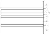
- the light emitting devicemay include a light emitting structure 10, as shown in FIG.
- the light emitting structure 10may include a first conductive semiconductor layer 11, an active layer 12, and a second conductive semiconductor layer 13.
- the active layer 12may be disposed between the first conductive semiconductor layer 11 and the second conductive semiconductor layer 13.
- the active layer 12may be disposed under the first conductive semiconductor layer 11, and the second conductive semiconductor layer 13 may be disposed under the active layer 12.
- the first conductivity type semiconductor layer 11is formed of an n type semiconductor layer to which an n type dopant is added as a first conductivity type dopant
- the second conductivity type semiconductor layer 13is a second conductivity type dopant.
- a p-type dopantmay be formed as a p-type semiconductor layer.
- the first conductive semiconductor layer 11may be formed of a p-type semiconductor layer
- the second conductive semiconductor layer 13may be formed of an n-type semiconductor layer.
- the first conductive semiconductor layer 11may include, for example, an n-type semiconductor layer.
- the first conductivity type semiconductor layer 11may be implemented as a compound semiconductor.
- the first conductivity type semiconductor layer 11may be implemented as, for example, a group II-VI compound semiconductor or a group III-V compound semiconductor.
- the first conductivity type semiconductor layer 11may be formed of a semiconductor material having a compositional formula of (Al x Ga 1-x ) y In 1-y P (0 ⁇ x ⁇ 1, 0 ⁇ y ⁇ 1). have.
- ymay have a value of 0.5
- xmay have a value of 0.5 to 0.8 in the composition formula.
- the first conductive semiconductor layer 11may be selected from, for example, AlGaInP, AlInP, GaP, GaInP, and the like, and may be doped with n-type dopants such as Si, Ge, Sn, Se, Te, or the like.
- the active layer 12In the active layer 12, electrons (or holes) injected through the first conductivity type semiconductor layer 11 and holes (or electrons) injected through the second conductivity type semiconductor layer 13 meet each other.
- the layeremits light due to a band gap difference of an energy band according to a material forming the active layer 12.
- the active layer 12may be formed of any one of a single well structure, a multiple well structure, a quantum dot structure, or a quantum line structure, but is not limited thereto.
- the active layer 12may be implemented with a compound semiconductor.
- the active layer 12may be implemented as, for example, a group II-VI or group III-V compound semiconductor.
- the active layer 12may be formed of a semiconductor material having, for example, a composition formula of (Al x Ga 1-x ) y In 1-y P (0 ⁇ x ⁇ 1, 0 ⁇ y ⁇ 1).
- the active layer 12may be selected from, for example, AlGaInP, AlInP, GaP, GaInP, or the like.
- the active layer 12may be implemented by stacking a plurality of well layers and a plurality of barrier layers.
- the second conductive semiconductor layer 13may be implemented with, for example, a p-type semiconductor layer.
- the second conductivity type semiconductor layer 13may be implemented as a compound semiconductor.
- the second conductivity-type semiconductor layer 13may be implemented by, for example, a group II-VI compound semiconductor or a group III-V compound semiconductor.
- the second conductivity-type semiconductor layer 13may be formed of a semiconductor material having a compositional formula of (Al x Ga 1-x ) y In 1-y P (0 ⁇ x ⁇ 1, 0 ⁇ y ⁇ 1). have.
- the second conductive semiconductor layer 13may be selected from, for example, AlGaInP, AlInP, GaP, GaInP, and the like, and may be doped with p-type dopants such as Mg, Zn, Ca, Sr, Ba, and C.
- the light emitting structure 10may include at least two elements selected from aluminum (Al), gallium (Ga), indium (In), and phosphorus (P).
- the first conductive semiconductor layer 11may include a p-type semiconductor layer
- the second conductive semiconductor layer 13may include an n-type semiconductor layer.
- a semiconductor layer including an n-type or p-type semiconductor layermay be further formed below the second conductive semiconductor layer 13.
- the light emitting structure 10may have at least one of np, pn, npn, and pnp junction structures.
- the doping concentrations of the impurities in the first conductive semiconductor layer 11 and the second conductive semiconductor layer 13may be uniformly or non-uniformly formed. That is, the structure of the light emitting structure 10 may be formed in various ways, but is not limited thereto.
- the active layer 12may include a plurality of barrier layers and a plurality of well layers.
- the active layer 12may include a barrier layer having a region not doped with impurities and a region doped with impurities.
- the barrier layer of the active layer 12may be doped with n-type impurities.
- the barrier layer and the well layer of the active layer 12may be provided with an AlGaInP composition, and the Al composition included in the barrier layer may have a larger value than that of the Al composition included in the well layer.
- FIG. 2shows an example of an active layer structure applied to a light emitting device according to an embodiment.
- the active layer 12includes a first barrier layer 31, a second barrier layer 32, a third barrier layer 33, and a fourth barrier layer 34. It may include.
- the active layer 12may include a first well layer 41, a second well layer 42, and a third well layer 43.
- the first well layer 41may be disposed between the first barrier layer 31 and the second barrier layer 32.
- the second well layer 42may be disposed between the second barrier layer 32 and the third barrier layer 33.
- the third well layer 43may be disposed between the third barrier layer 33 and the fourth barrier layer 44.
- impuritiesmay not be doped into the first barrier layer 31.
- An impuritymay be doped into the second barrier layer 32.
- the second barrier layer 32may be disposed under the first barrier layer 31 and may include a region having a different doping concentration of impurities according to a distance from the first barrier layer 31. Impurities may not be doped in the third barrier layer 33.
- the second barrier layer 32may include a first region 51 not doped with impurities, a second region 52 doped with impurities, and a third region 53 not doped with impurities.
- the second region 52may be disposed below the first region 51, and the third region 53 may be disposed below the second region 52.
- An n-type impuritymay be doped in the second region 52.
- the first region 51may be thicker than the second region 52.
- the third region 53may be provided to have the same thickness as the first region 51.
- the first region 51may be continuously disposed in the second region 52, and the second region 52 may be continuously disposed in the third region 53.
- the second region 52may be provided at a thickness of 18 angstroms to 22 angstroms.
- the first region 51 and the third region 53may be provided at a thickness of 75 angstroms to 85 angstroms.
- the second region 52may be doped with an n-type impurity, and an impurity doping concentration may be implemented as, for example, 1 ⁇ 10 16 / cm 3 to 5 ⁇ 10 16 / cm 3. Impurities included in the second region 52 may increase electron mobility in the active layer 12, thereby increasing light extraction efficiency by increasing electron-hole coupling efficiency.
- the thickness of the second region 52may be provided as a thickness of, for example, 10% to 50% of the total thickness of the second barrier layer 32.
- the thickness of the second region 52is thinner than 10% of the thickness of the barrier layer, the improvement of characteristics due to the impurities doped in the region of the second region 52 may not appear much.
- the thickness of the second region 52is thicker than 50% of the barrier layer thickness, the quality of the active layer may be degraded due to excessively doped impurities in the barrier layer, and the light intensity is deteriorated due to light absorption. May be generated.
- the first barrier layer 31, the second barrier layer 32, the third barrier layer 33, and the fourth barrier layer 34may be provided to have a thickness of 170 angstroms to 190 angstroms, respectively.
- the first well layer 41, the second well layer 42, and the third well layer 43may be provided in a thickness of 65 angstroms to 75 angstroms, respectively.
- the active layer 12is a pair of the first barrier layer 31 and the first well layer 41, a pair of the second barrier layer 32 and the second well layer 42, A plurality of pairs of the third barrier layer 33 and the third well layer 43 may be included.
- the pair of the first barrier layer 31 and the first well layer 41is repeated seven times, followed by the pair of the second barrier layer 32 and the second well layer 42 six times.
- the third barrier layer 33 and the third well layer 43may be repeatedly disposed seven times.
- the light emitting devicemay include the window layer 15.
- the window layer 15may be disposed under the second conductivity type semiconductor layer 13.
- the window layer 15may be formed of a semiconductor material having a compositional formula of (Al x Ga 1-x ) y In 1-y P (0 ⁇ x ⁇ 1, 0 ⁇ y ⁇ 1).
- the window layer 15may be selected from, for example, AlGaInP, AlInP, GaP, GaInP, or the like.
- the window layer 15may provide a current spreading effect.
- the window layer 15may include impurities.
- the window layer 15may include impurities having the same polarity as that of the second conductivity-type semiconductor layer 13.
- the light emitting devicemay include an omni directional reflector (ODR) layer 21, an ohmic contact layer 23, and a reflective layer 30.
- ODRomni directional reflector
- the ODR layer 21may perform a function of reflecting light incident from an upper direction upward.
- the ODR layer 21may be implemented to have a lower refractive index than the light emitting structure 10.
- the ODR layer 21may be selected to have a low refractive index having a large difference from the refractive index of the material of the light emitting structure 10, thereby providing a reflective function.
- the ODR layer 21may be disposed in contact with the window layer 15.
- the ODR layer 21may include an oxide or a nitride.
- the ODR layer 21includes, for example, SiO 2 , SiN x , Indium-Tin-Oxide (ITO), Indium-Zinc-Oxide (IZO), Aluminum-Zinc-Oxide (AZO), and Antimony-Tin-Oxide (ATO).
- ITOIndium-Tin-Oxide
- IZOIndium-Zinc-Oxide
- AZOAluminum-Zinc-Oxide
- ATOAntimony-Tin-Oxide
- IZTOIndium-Zinc-Tin-Oxide
- IAZOIndium-Aluminum-Zinc-Oxide
- GZOGadium-Zinc-Oxide
- IGZOIndium-Gallium-Zinc-Oxide
- IGTOIndium-Gallium-Oxide
- Tin-OxideZinc-Oxide
- AZOAlluminanum-Zinc-Oxide
- the ohmic contact layer 23may be implemented to be in ohmic contact with the window layer 15.
- the ohmic contact layer 23may include an area in ohmic contact with the window layer 15.
- the ohmic contact layer 23may be electrically connected to the light emitting structure 10.
- the ohmic contact layer 23may be disposed through the ODR layer 21.
- the ohmic contact layer 23may be provided in a through hole penetrating the upper and lower surfaces of the ODR layer 21.
- the ohmic contact layer 23may be implemented to have an upper surface of a circle or ellipse shape.
- the ohmic contact layer 23may include at least one selected from materials such as Au, Au / AuBe / Au, AuZn, ITO, AuBe, and GeAu.
- the reflective layer 30may be disposed under the ohmic contact layer 23.
- the reflective layer 30may be disposed under the ODR layer 21.
- the reflective layer 30may perform a function of reflecting light incident from an upper direction in an upper direction.
- the reflective layer 30may include at least one selected from materials such as Ag, Au, and Al.
- the light emitting devicemay include a bonding layer 40 and a support substrate 50.
- the bonding layer 40may perform a function of attaching the reflective layer 30 to the support substrate 50.
- the bonding layer 40is, for example, a material such as Sn, AuSn, Pd, Al, Ti, Au, Ni, Cr, Ga, In, Bi, Cu, Ag, Nb, Ta, Ti / Au / In / Au It may include at least one selected from among.
- the support substrate 50may be a semiconductor substrate in which Ti, Cr, Ni, Al, Pt, Au, W, Cu, Mo, Cu-W, or impurities are implanted (eg, Si, Ge, GaN, GaAs, ZnO, SiC, SiGe and the like) may be included.
- the light emitting devicemay include a first electrode 60 and an electrode pad 70 disposed on the light emitting structure 10.
- the first electrode 60may be electrically connected to the first conductivity type semiconductor layer 11.
- the first electrode 60may be disposed in contact with the first conductive semiconductor layer 11.
- the first electrode 60may be disposed in ohmic contact with the first conductivity-type semiconductor layer 11.
- the first electrode 60may include a region in ohmic contact with the light emitting structure 10.
- the first electrode 60may include a region in ohmic contact with the first conductivity-type semiconductor layer 11.
- the first electrode 60may include at least one selected from Ge, Zn, Mg, Ca, Au, Ni, AuGe, AuGe / Ni / Au, and the like.
- the first electrode 60may be provided in a single layer or a multilayer structure.
- a high concentration impurity semiconductor layermay be further included between the first electrode 60 and the first conductivity type semiconductor layer 11.
- a GaAs layermay be further disposed between the first electrode 60 and the first conductivity type semiconductor layer 11, and may include a GaAs layer containing a higher concentration impurity than the impurity concentration of the first conductivity type semiconductor layer 11. have.
- the electrode pad 70may be electrically connected to the first electrode 60.
- the electrode pad 70may be disposed on the first electrode 60.
- the electrode pad 70may be disposed in contact with the first electrode 60.
- the electrode pad 70may be connected to an external power source to provide power to the light emitting structure 10.
- the electrode pad 70is formed of Cr, V, W, Ti, Zn, Ni, Cu, Al, Au, Mo, Ti / Au / Ti / Pt / Au, Ni / Au / Ti / Pt / Au, Cr / Al It may include at least any one selected from / Ni / Cu / Ni / Au.
- the electrode pad 70may be provided in a single layer or a multilayer structure.
- the light emitting devicemay include a protective layer 80.
- the protective layer 80may be disposed on the light emitting structure 10.
- the protective layer 80may be disposed around the light emitting structure 10.
- the protective layer 80may be disposed on the side surface of the light emitting structure 10.
- the protective layer 80may be disposed around the window layer 15. Some areas of the protective layer 80 may be disposed on some areas of the window layer 15.
- the protective layer 80may be disposed on the first conductivity type semiconductor layer 11.
- the protective layer 80may be disposed on the first electrode 60.
- the protective layer 80may include a light extraction structure provided on an upper surface.
- the light extraction structuremay be referred to as an uneven structure, and may also be referred to as roughness.
- the light extracting structuresmay be arranged regularly, or may be arranged randomly.
- the light extraction structure provided on the upper surface of the protective layer 80may be formed in a shape corresponding to the light extraction structure provided on the upper surface of the first conductive semiconductor layer 11.
- the protective layer 80may include at least one of an oxide or a nitride. At least one of the protective layer 80 is selected from the group consisting of Si0 2 , Si x O y , Si 3 N 4 , Si x N y , SiO x N y , Al 2 O 3 , TiO 2 , AlN, and the like. Can be formed.
- the support substrate 50may be implemented to have conductivity.
- the support substrate 50may be connected to an external power source, and thus power may be applied to the light emitting structure 10 through the support substrate 50.
- Powermay be applied to the second conductive semiconductor layer 13 through the support substrate 50.
- a second electrodemay be electrically connected to the second conductivity type semiconductor layer 13.
- the second electrodemay include at least one of the ohmic contact layer 23, the reflective layer 30, the bonding layer 40, and the support substrate 50.
- a barrier layer in which impurities are added to the central portion of the active layer 12may be disposed to increase electron mobility in the active layer 12.
- the light emitting device according to the embodimentmay include a barrier layer in which impurities are added to the inside of the active layer 12. Accordingly, the light emitting device according to the embodiment may increase the electron-hole coupling efficiency, thereby increasing the internal light emitting efficiency. In addition, the light emitting device according to the embodiment may improve the operating voltage, the overall light extraction efficiency.
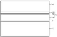
- the etch stop layer 7the first conductivity type semiconductor layer 11, the active layer 12, and the second conductivity type on the substrate 5.
- the semiconductor layer 13 and the window layer 15may be formed.
- the first conductive semiconductor layer 11, the active layer 12, and the second conductive semiconductor layer 13may be defined as a light emitting structure 10.
- the substrate 5may be formed of, for example, at least one of sapphire substrate (Al 2 O 3 ), SiC, GaAs, GaN, ZnO, Si, GaP, InP, Ge, but is not limited thereto.
- a buffer layermay be further formed between the substrate 5 and the etch stop layer 7.
- the etch stop layer 7may be formed of, for example, a semiconductor material having a compositional formula of (Al x Ga 1-x ) y In 1-y P (0 ⁇ x ⁇ 1, 0 ⁇ y ⁇ 1). The function of the etch stop layer 7 will be described later.
- the first conductivity type semiconductor layer 11is formed of an n type semiconductor layer to which an n type dopant is added as a first conductivity type dopant
- the second conductivity type semiconductor layer 13is a second conductivity type. It may be formed of a p-type semiconductor layer to which a p-type dopant is added as a type dopant.
- the first conductive semiconductor layer 11may be formed of a p-type semiconductor layer
- the second conductive semiconductor layer 13may be formed of an n-type semiconductor layer.
- the first conductive semiconductor layer 11may include, for example, an n-type semiconductor layer.
- the first conductivity type semiconductor layer 11may be implemented as a compound semiconductor.
- the first conductivity type semiconductor layer 11may be implemented as, for example, a group II-VI compound semiconductor or a group III-V compound semiconductor.
- the first conductivity type semiconductor layer 11may be formed of a semiconductor material having a compositional formula of (Al x Ga 1-x ) y In 1-y P (0 ⁇ x ⁇ 1, 0 ⁇ y ⁇ 1). have.
- ymay have a value of 0.5
- xmay have a value of 0.5 to 0.8 in the compositional formula.
- the first conductive semiconductor layer 11may be selected from, for example, AlGaInP, AlInP, GaP, GaInP, and the like, and may be doped with n-type dopants such as Si, Ge, Sn, Se, Te, or the like.
- the active layer 12In the active layer 12, electrons (or holes) injected through the first conductivity type semiconductor layer 11 and holes (or electrons) injected through the second conductivity type semiconductor layer 13 meet each other.
- the layeremits light due to a band gap difference of an energy band according to a material forming the active layer 12.
- the active layer 12may be formed of any one of a single well structure, a multiple well structure, a quantum dot structure, or a quantum line structure, but is not limited thereto.
- the active layer 12may be implemented with a compound semiconductor.
- the active layer 12may be implemented as, for example, a group II-VI or group III-V compound semiconductor.
- the active layer 12may be formed of a semiconductor material having, for example, a composition formula of (Al x Ga 1-x ) y In 1-y P (0 ⁇ x ⁇ 1, 0 ⁇ y ⁇ 1).
- the active layer 12may be selected from, for example, AlGaInP, AlInP, GaP, GaInP, or the like.
- the active layer 12may be implemented by stacking a plurality of well layers and a plurality of barrier layers.
- the second conductive semiconductor layer 13may be implemented with, for example, a p-type semiconductor layer.
- the second conductivity type semiconductor layer 13may be implemented as a compound semiconductor.
- the second conductivity-type semiconductor layer 13may be implemented by, for example, a group II-VI compound semiconductor or a group III-V compound semiconductor.
- the second conductivity-type semiconductor layer 13may be formed of a semiconductor material having a compositional formula of (Al x Ga 1-x ) y In 1-y P (0 ⁇ x ⁇ 1, 0 ⁇ y ⁇ 1). have.
- the second conductive semiconductor layer 13may be selected from, for example, AlGaInP, AlInP, GaP, GaInP, and the like, and may be doped with p-type dopants such as Mg, Zn, Ca, Sr, Ba, and C.
- the light emitting structure 10may include at least two elements selected from aluminum (Al), gallium (Ga), indium (In), and phosphorus (P).
- the active layer 12may include a plurality of barrier layers and a plurality of well layers.
- the active layer 12may include a barrier layer having a region not doped with impurities and a region doped with impurities.
- the barrier layer of the active layer 12may be doped with n-type impurities.
- the barrier layer and the well layer of the active layer 12may be provided with an AlGaInP composition, and the Al composition included in the barrier layer may have a larger value than that of the Al composition included in the well layer.
- the window layer 15may be formed of a semiconductor material having a compositional formula of (Al x Ga 1-x ) y In 1-y P (0 ⁇ x ⁇ 1, 0 ⁇ y ⁇ 1).
- the window layer 15may be selected from, for example, AlGaInP, AlInP, GaP, GaInP, or the like.
- the window layer 15may provide a current spreading effect when the light emitting device is driven.
- an ODR layer 21, an ohmic contact layer 23, and a reflective layer 30may be formed on the window layer 15.
- the ODR layer 21may perform a function of reflecting incident light again.
- the ODR layer 21may be implemented to have a lower refractive index than the light emitting structure 10.
- the ODR layer 21may be selected to have a low refractive index having a large difference from the refractive index of the material of the light emitting structure 10, thereby providing a reflective function.
- the ODR layer 21may be disposed in contact with the window layer 15.
- the ODR layer 21may include an oxide or a nitride.
- the ODR layer 21may include, for example, SiO 2 , SiNx, ITO (Indium-Tin-Oxide), IZO (Indium-Zinc-Oxide), AZO (Aluminum-Zinc-Oxide), ATO (Antimony-Tin-Oxide) , Indium-Zinc-Tin-Oxide (IZTO), Indium-Aluminum-Zinc-Oxide (IAZO), Gallium-Zinc-Oxide (GZO), Indium-Gallium-Zinc-Oxide (IGZO), Indium-Gallium-Tin -Oxide), AZO (Aluminum-Zinc-Oxide) may include at least one selected from materials.
- the ohmic contact layer 23may be implemented to be in ohmic contact with the window layer 15.
- the ohmic contact layer 23may include an area in ohmic contact with the window layer 15.
- the ohmic contact layer 23may be electrically connected to the light emitting structure 10.
- the ohmic contact layer 23may be disposed through the ODR layer 21.
- the ohmic contact layer 23may be implemented to have an upper surface of a circle or ellipse shape.
- the ohmic contact layer 23may include at least one selected from materials such as Au, Au / AuBe / Au, AuZn, ITO, AuBe, and GeAu.
- the reflective layer 30may be disposed on the ohmic contact layer 23.
- the reflective layer 30may be disposed on the ODR layer 21.
- the reflective layer 30may perform a function of reflecting incident light again.
- the reflective layer 30may include at least one selected from materials such as Ag, Au, and Al.
- a bonding layer 40 and a support substrate 50may be provided on the reflective layer 30.
- the bonding layer 40may perform a function of attaching the reflective layer 30 to the support substrate 50.
- the bonding layer 40is, for example, a material such as Sn, AuSn, Pd, Al, Ti, Au, Ni, Cr, Ga, In, Bi, Cu, Ag, Nb, Ta, Ti / Au / In / Au It may include at least one selected from among.
- the support substrate 50may be a semiconductor substrate in which Ti, Cr, Ni, Al, Pt, Au, W, Cu, Mo, Cu-W, or impurities are implanted (eg, Si, Ge, GaN, GaAs, ZnO, SiC, SiGe and the like) may be included.
- the substrate 5is removed from the etch stop layer 7.
- the substrate 5may be removed by an etching process.
- the substrate 5may be removed by a wet etching process, and the etch stop layer 7 is not etched so that only the substrate 5 is etched and separated. Can serve as a stop layer.
- the etch stop layer 7may be separated from the light emitting structure 10 through a separate removal process.
- the etch stop layer 7may be removed through a separate etching process.
- a first electrode 60may be formed on the light emitting structure 10, and isolation etching may be performed to etch the side surface of the light emitting structure 10.
- the first electrode 60may be electrically connected to the first conductivity type semiconductor layer 11.
- the first electrode 60may be disposed in contact with the first conductive semiconductor layer 11.
- the first electrode 60may be disposed in ohmic contact with the first conductivity-type semiconductor layer 11.
- the first electrode 60may include a region in ohmic contact with the light emitting structure 10.
- the first electrode 60may include a region in ohmic contact with the first conductivity-type semiconductor layer 11.
- the first electrode 60may include at least one selected from Ge, Zn, Mg, Ca, Au, Ni, AuGe, AuGe / Ni / Au, and the like.
- the passivation layer 80 and the electrode pad 70may be formed on the light emitting structure 10 and the first electrode 60.
- the protective layer 80may be disposed on the light emitting structure 10.
- the protective layer 80may be disposed around the light emitting structure 10.
- the protective layer 80may be disposed on the side surface of the light emitting structure 10.
- the protective layer 80may be disposed around the window layer 15. Some areas of the protective layer 80 may be disposed on some areas of the window layer 15.
- the protective layer 80may include at least one of an oxide or a nitride. At least one of the protective layer 80 is selected from the group consisting of Si0 2 , Si x O y , Si 3 N 4 , Si x N y , SiO x N y , Al 2 O 3 , TiO 2 , AlN, and the like. Can be formed.
- the protective layer 80may be disposed on the first conductivity type semiconductor layer 11.
- the protective layer 80may be disposed on the first electrode 60.
- the protective layer 80may include a light extraction structure provided on an upper surface.
- the light extraction structuremay be referred to as an uneven structure, and may also be referred to as roughness.
- the light extracting structuresmay be arranged regularly, or may be arranged randomly.
- the electrode pad 70may be electrically connected to the first electrode 60.
- the electrode pad 70may be disposed on the first electrode 60.
- the electrode pad 70may be disposed in contact with the first electrode 60.
- the electrode pad 70may be connected to an external power source to provide power to the light emitting structure 10.
- the electrode pad 70is formed of Cr, V, W, Ti, Zn, Ni, Cu, Al, Au, Mo, Ti / Au / Ti / Pt / Au, Ni / Au / Ti / Pt / Au, Cr / Al It may include at least any one selected from / Ni / Cu / Ni / Au.
- the light emitting device manufacturing method described abovemay be modified and implemented according to the process design as needed.
- a barrier layer in which impurities are added to the central portion of the active layer 12may be disposed to increase electron mobility in the active layer 12. Accordingly, the light emitting device according to the embodiment may increase the electron-hole coupling efficiency, thereby increasing the internal light emitting efficiency. In addition, the light emitting device according to the embodiment may improve the operating voltage, the overall light extraction efficiency can be improved.
- FIG. 7is a view showing a light emitting device package to which the light emitting device according to the embodiment is applied.
- the light emitting device packagemay include a body 120, a first lead electrode 131 and a second lead electrode 132 disposed on the body 120, and the body 120.
- the light emitting device 100 according to the embodimentwhich is provided to and electrically connected to the first lead electrode 131 and the second lead electrode 132, and the molding member 140 surrounding the light emitting device 100. It may include.
- the body 120may include a silicon material, a synthetic resin material, or a metal material, and an inclined surface may be formed around the light emitting device 100.
- the first lead electrode 131 and the second lead electrode 132are electrically separated from each other, and provide power to the light emitting device 100.
- the first lead electrode 131 and the second lead electrode 132may increase light efficiency by reflecting light generated from the light emitting device 100, and heat generated from the light emitting device 100. It may also play a role in discharging it to the outside.
- the light emitting device 100may be disposed on the body 120 or on the first lead electrode 131 or the second lead electrode 132.
- the light emitting device 100may be electrically connected to the first lead electrode 131 and the second lead electrode 132 by any one of a wire method, a flip chip method, and a die bonding method.
- the molding member 140may surround the light emitting device 100 to protect the light emitting device 100.
- the molding member 140may include a phosphor to change the wavelength of light emitted from the light emitting device 100.
- a plurality of light emitting devices or light emitting device packagesmay be arranged on a substrate, and an optical member such as a lens, a light guide plate, a prism sheet, and a diffusion sheet may be disposed on an optical path of the light emitting device package.
- the light emitting device package, the substrate, and the optical membermay function as a light unit.
- the light unitmay be implemented in a top view or a side view type, and may be provided in a display device such as a portable terminal and a notebook computer, or may be variously applied to an illumination device and a pointing device.
- Yet another embodimentmay be implemented as a lighting device including the light emitting device or the light emitting device package described in the above embodiments.
- the lighting devicemay include a lamp, a street lamp, a signboard, a headlamp.
- the light emitting devicemay be applied to the light unit.
- the light unitmay include a structure in which a plurality of light emitting elements are arranged, and may include the display device illustrated in FIGS. 8 and 9 and the illumination device illustrated in FIG. 10.
- the display device 1000includes a light guide plate 1041, a light emitting module 1031 that provides light to the light guide plate 1041, and a reflective member 1022 under the light guide plate 1041. ), An optical sheet 1051 on the light guide plate 1041, a display panel 1061, a light guide plate 1041, a light emitting module 1031, and a reflective member 1022 on the optical sheet 1051.
- the bottom cover 1011may be included, but is not limited thereto.
- the bottom cover 1011, the reflective sheet 1022, the light guide plate 1041, and the optical sheet 1051may be defined as a light unit 1050.
- the light guide plate 1041diffuses light to serve as a surface light source.
- the light guide plate 1041is made of a transparent material, for example, acrylic resin-based such as polymethyl metaacrylate (PMMA), polyethylene terephthlate (PET), polycarbonate (PC), cycloolefin copolymer (COC), and polyethylene naphthalate (PEN). It may include one of the resins.
- PMMApolymethyl metaacrylate
- PETpolyethylene terephthlate
- PCpolycarbonate
- COCcycloolefin copolymer
- PENpolyethylene naphthalate
- the light emitting module 1031provides light to at least one side of the light guide plate 1041, and ultimately serves as a light source of the display device.
- At least one light emitting module 1031may be provided, and may provide light directly or indirectly at one side of the light guide plate 1041.
- the light emitting module 1031may include a substrate 1033 and a light emitting device or a light emitting device package 200 according to the embodiment described above.
- the light emitting device package 200may be arranged on the substrate 1033 at predetermined intervals.
- the substrate 1033may be a printed circuit board (PCB) including a circuit pattern.
- the substrate 1033may include not only a general PCB but also a metal core PCB (MCPCB, Metal Core PCB), a flexible PCB (FPCB, Flexible PCB) and the like, but is not limited thereto.
- MCPCBMetal Core PCB
- FPCBFlexible PCB
- the substrate 1033may be removed.
- a part of the heat dissipation platemay contact the upper surface of the bottom cover 1011.
- the plurality of light emitting device packages 200may be mounted such that an emission surface from which light is emitted is spaced apart from the light guide plate 1041 by a predetermined distance, but is not limited thereto.
- the light emitting device package 200may directly or indirectly provide light to a light incident portion that is one side of the light guide plate 1041, but is not limited thereto.
- the reflective member 1022may be disposed under the light guide plate 1041.
- the reflective member 1022may improve the luminance of the light unit 1050 by reflecting light incident to the lower surface of the light guide plate 1041 and pointing upward.
- the reflective member 1022may be formed of, for example, PET, PC, or PVC resin, but is not limited thereto.
- the reflective member 1022may be an upper surface of the bottom cover 1011, but is not limited thereto.
- the bottom cover 1011may accommodate the light guide plate 1041, the light emitting module 1031, the reflective member 1022, and the like. To this end, the bottom cover 1011 may be provided with an accommodating part 1012 having a box shape having an upper surface opened thereto, but is not limited thereto. The bottom cover 1011 may be combined with the top cover, but is not limited thereto.
- the bottom cover 1011may be formed of a metal material or a resin material, and may be manufactured using a process such as press molding or extrusion molding.
- the bottom cover 1011may include a metal or non-metal material having good thermal conductivity, but is not limited thereto.
- the display panel 1061is, for example, an LCD panel and includes a first and second substrates of transparent materials facing each other, and a liquid crystal layer interposed between the first and second substrates.
- a polarizermay be attached to at least one surface of the display panel 1061, but the polarizer is not limited thereto.
- the display panel 1061displays information by light passing through the optical sheet 1051.
- the display device 1000may be applied to various portable terminals, monitors of notebook computers, monitors of laptop computers, televisions, and the like.
- the optical sheet 1051is disposed between the display panel 1061 and the light guide plate 1041 and includes at least one light transmissive sheet.
- the optical sheet 1051may include at least one of a sheet such as, for example, a diffusion sheet, a horizontal and vertical prism sheet, and a brightness enhancement sheet.
- the diffusion sheetdiffuses the incident light
- the horizontal and / or vertical prism sheetfocuses the incident light into the display area
- the brightness enhancement sheetreuses the lost light to improve the brightness.
- a protective sheetmay be disposed on the display panel 1061, but is not limited thereto.
- the light guide plate 1041 and the optical sheet 1051may be included as an optical member on the optical path of the light emitting module 1031, but are not limited thereto.
- FIG. 9is a diagram illustrating another example of a display device according to an exemplary embodiment.
- the display device 1100includes a bottom cover 1152, a substrate 1020 on which the light emitting device 100 disclosed above is arranged, an optical member 1154, and a display panel 1155.
- the substrate 1020 and the light emitting device package 200may be defined as a light emitting module 1060.
- the bottom cover 1152may include an accommodating part 1153, but is not limited thereto.
- the optical member 1154may include at least one of a lens, a light guide plate, a diffusion sheet, horizontal and vertical prism sheets, and a brightness enhancement sheet.
- the light guide platemay be made of a PC material or a poly methy methacrylate (PMMA) material, and the light guide plate may be removed.
- the diffusion sheetdiffuses the incident light
- the horizontal and vertical prism sheetsfocus the incident light onto the display area
- the brightness enhancement sheetreuses the lost light to improve the brightness.
- the optical member 1154is disposed on the light emitting module 1060, and performs surface light source, diffusion, condensing, etc. of the light emitted from the light emitting module 1060.
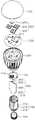
- FIG. 10is a view showing a lighting apparatus according to an embodiment.
- the lighting apparatusmay include a cover 2100, a light source module 2200, a radiator 2400, a power supply 2600, an inner case 2700, and a socket 2800. Can be.
- the lighting apparatus according to the embodimentmay further include any one or more of the member 2300 and the holder 2500.
- the light source module 2200may include a light emitting device package according to an embodiment.
- the cover 2100may have a shape of a bulb or hemisphere, may be hollow, and may be provided in an open shape.
- the cover 2100may be optically coupled to the light source module 2200.
- the cover 2100may diffuse, scatter or excite the light provided from the light source module 2200.
- the cover 2100may be a kind of optical member.
- the cover 2100may be coupled to the heat sink 2400.
- the cover 2100may have a coupling part coupled to the heat sink 2400.
- An inner surface of the cover 2100may be coated with a milky paint.
- the milky paintmay include a diffuser to diffuse light.
- the surface roughness of the inner surface of the cover 2100may be greater than the surface roughness of the outer surface of the cover 2100. This is for the light from the light source module 2200 to be sufficiently scattered and diffused to be emitted to the outside.
- the cover 2100may be made of glass, plastic, polypropylene (PP), polyethylene (PE), polycarbonate (PC), or the like.
- polycarbonateis excellent in light resistance, heat resistance, and strength.
- the cover 2100may be transparent and opaque so that the light source module 2200 is visible from the outside.
- the cover 2100may be formed through blow molding.
- the light source module 2200may be disposed on one surface of the heat sink 2400. Thus, heat from the light source module 2200 is conducted to the heat sink 2400.
- the light source module 2200may include a light source unit 2210, a connection plate 2230, and a connector 2250.
- the member 2300is disposed on an upper surface of the heat dissipator 2400, and has a plurality of light source parts 2210 and guide grooves 2310 into which the connector 2250 is inserted.
- the guide groove 2310corresponds to the board and the connector 2250 of the light source unit 2210.
- the surface of the member 2300may be coated or coated with a light reflective material.
- the surface of the member 2300may be coated or coated with a white paint.
- the member 2300is reflected on the inner surface of the cover 2100 to reflect the light returned to the light source module 2200 side again toward the cover 2100. Therefore, it is possible to improve the light efficiency of the lighting apparatus according to the embodiment.
- the member 2300may be made of an insulating material, for example.
- the connection plate 2230 of the light source module 2200may include an electrically conductive material. Therefore, electrical contact may be made between the radiator 2400 and the connection plate 2230.
- the member 2300may be formed of an insulating material to block an electrical short between the connection plate 2230 and the radiator 2400.
- the radiator 2400receives heat from the light source module 2200 and heat from the power supply unit 2600 to radiate heat.
- the holder 2500may block the accommodating groove 2719 of the insulating portion 2710 of the inner case 2700. Therefore, the power supply unit 2600 accommodated in the insulating unit 2710 of the inner case 2700 is sealed.
- the holder 2500has a guide protrusion 2510.
- the guide protrusion 2510has a hole through which the protrusion 2610 of the power supply unit 2600 passes.
- the power supply unit 2600processes or converts an electrical signal provided from the outside to provide the light source module 2200.
- the power supply unit 2600is accommodated in the accommodating groove 2725 of the inner case 2700, and is sealed in the inner case 2700 by the holder 2500.
- the power supply unit 2600may include a protrusion 2610, a guide unit 2630, a base 2650, and an extension unit 2670.
- the guide part 2630has a shape protruding outward from one side of the base 2650.
- the guide part 2630may be inserted into the holder 2500.
- a plurality of partsmay be disposed on one surface of the base 2650.
- the plurality of componentsmay include, for example, a DC converter for converting AC power provided from an external power source into DC power, a driving chip for controlling the driving of the light source module 2200, and an ESD for protecting the light source module 2200. (ElectroStatic discharge) protection element and the like, but may not be limited thereto.
- the extension part 2670has a shape protruding outward from the other side of the base 2650.
- the extension part 2670is inserted into the connection part 2750 of the inner case 2700 and receives an electrical signal from the outside.
- the extension part 2670may be provided to be equal to or smaller than the width of the connection part 2750 of the inner case 2700.
- Each end of the "+ wire” and the “-wire”may be electrically connected to the extension 2670, and the other end of the "+ wire” and the “-wire” may be electrically connected to the socket 2800. .
- the inner case 2700may include a molding unit together with the power supply unit 2600 therein.
- the molding partis a part where the molding liquid is hardened, so that the power supply part 2600 can be fixed inside the inner case 2700.
- the light emitting device, the light emitting device package, and the light unit according to the embodimenthave an advantage of lowering an operating voltage and improving brightness.
Landscapes
- Led Devices (AREA)
Abstract
Description
Translated fromKorean실시 예는 발광소자, 발광소자 패키지 및 라이트 유닛에 관한 것이다.Embodiments relate to a light emitting device, a light emitting device package, and a light unit.
발광소자의 예로서 레이저 다이오드(LD: Laser Diode)와 발광 다이오드(LED: Light Emitting Diode)가 많이 사용되고 있다. 발광소자는 화합물 반도체의 특성을 이용해 전기 신호를 적외선, 가시광선, 자외선과 같은 빛의 형태로 변환한다.As an example of a light emitting device, a laser diode (LD) and a light emitting diode (LED) are used. The light emitting device converts an electrical signal into a form of light such as infrared rays, visible rays, and ultraviolet rays using characteristics of the compound semiconductor.
발광소자의 광 효율이 증가됨에 따라 표시장치, 조명기기를 비롯한 다양한 분야에 발광소자가 적용되고 있다.As the light efficiency of light emitting devices increases, light emitting devices have been applied to various fields including display devices and lighting devices.
실시 예는 동작 전압을 낮추고 광도를 향상시킬 수 있는 발광소자, 발광소자 패키지, 라이트 유닛을 제공한다.The embodiment provides a light emitting device, a light emitting device package, and a light unit capable of lowering an operating voltage and improving brightness.
실시 예에 따른 발광소자는, 제1 도전형 반도체층; 제2 도전형 반도체층; 상기 제1 도전형 반도체층과 상기 제2 도전형 반도체층 사이에 배치되며, 불순물이 도핑되지 않은 영역과 불순물이 도핑된 영역을 갖는 장벽층을 포함하는 활성층; 을 포함한다.The light emitting device according to the embodiment may include a first conductive semiconductor layer; A second conductivity type semiconductor layer; An active layer disposed between the first conductive semiconductor layer and the second conductive semiconductor layer, the active layer including a barrier layer having a region not doped with impurities and a region doped with impurities; It includes.
실시 예에 따른 발광소자는, 제1 도전형 반도체층; 상기 제1 도전형 반도체층 아래에 배치되며, 불순물이 도핑되지 않은 제1 장벽층, 상기 제1 장벽층 아래에 배치되며 상기 제1 장벽층으로부터의 거리에 따라 불순물의 도핑 농도가 다른 영역을 포함하는 제2 장벽층, 상기 제2 장벽층 아래에 배치되며 불순물이 도핑되지 않은 제3 장벽층을 갖는 장벽층을 포함하는 활성층; 상기 활성층 아래에 배치된 제2 도전형 반도체층; 상기 제2 도전형 반도체층 아래에 배치된 윈도우층; 을 포함한다.The light emitting device according to the embodiment may include a first conductive semiconductor layer; A first barrier layer disposed under the first conductivity type semiconductor layer, the first barrier layer not doped with impurities, and a region disposed below the first barrier layer and having a different doping concentration of impurities depending on a distance from the first barrier layer An active layer comprising a second barrier layer, a barrier layer disposed below the second barrier layer, the barrier layer having a third barrier layer that is not doped with impurities; A second conductivity type semiconductor layer disposed under the active layer; A window layer disposed under the second conductivity type semiconductor layer; It includes.
실시 예에 따른 발광소자 패키지는, 몸체; 상기 몸체에 배치된 제1 리드전극 및 제2 리드전극; 상기 몸체에 제공되어 상기 제1 리드전극 및 제2 리드전극과 전기적으로 연결된 발광소자; 를 포함하고, 상기 발광소자는, 제1 도전형 반도체층, 제2 도전형 반도체층, 상기 제1 도전형 반도체층과 상기 제2 도전형 반도체층 사이에 배치되며 불순물이 도핑되지 않은 영역과 불순물이 도핑된 영역을 갖는 장벽층을 포함하는 활성층을 포함한다.The light emitting device package according to the embodiment includes a body; First and second lead electrodes disposed on the body; A light emitting device provided on the body and electrically connected to the first lead electrode and the second lead electrode; The light emitting device includes a first conductive semiconductor layer, a second conductive semiconductor layer, a region disposed between the first conductive semiconductor layer and the second conductive semiconductor layer and which is not doped with impurities. An active layer comprising a barrier layer having this doped region.
실시 예에 따른 발광소자 패키지는, 몸체; 상기 몸체에 배치된 제1 리드전극 및 제2 리드전극; 상기 몸체에 제공되어 상기 제1 리드전극 및 제2 리드전극과 전기적으로 연결된 발광소자; 를 포함하고, 상기 발광소자는, 제1 도전형 반도체층; 상기 제1 도전형 반도체층 아래에 배치되며, 불순물이 도핑되지 않은 제1 장벽층, 상기 제1 장벽층 아래에 배치되며 상기 제1 장벽층으로부터의 거리에 따라 불순물의 도핑 농도가 다른 영역을 포함하는 제2 장벽층, 상기 제2 장벽층 아래에 배치되며 불순물이 도핑되지 않은 제3 장벽층을 갖는 장벽층을 포함하는 활성층; 상기 활성층 아래에 배치된 제2 도전형 반도체층; 상기 제2 도전형 반도체층 아래에 배치된 윈도우층; 을 포함한다.The light emitting device package according to the embodiment includes a body; First and second lead electrodes disposed on the body; A light emitting device provided on the body and electrically connected to the first lead electrode and the second lead electrode; The light emitting device includes: a first conductivity type semiconductor layer; A first barrier layer disposed under the first conductivity type semiconductor layer, the first barrier layer not doped with impurities, and a region disposed below the first barrier layer and having a different doping concentration of impurities depending on a distance from the first barrier layer An active layer comprising a second barrier layer, a barrier layer disposed below the second barrier layer, the barrier layer having a third barrier layer that is not doped with impurities; A second conductivity type semiconductor layer disposed under the active layer; A window layer disposed under the second conductivity type semiconductor layer; It includes.
실시 예에 따른 라이트 유닛은, 몸체; 상기 몸체에 배치된 제1 리드전극 및 제2 리드전극; 상기 몸체에 제공되어 상기 제1 리드전극 및 제2 리드전극과 전기적으로 연결된 발광소자; 를 포함하고, 상기 발광소자는, 제1 도전형 반도체층, 제2 도전형 반도체층, 상기 제1 도전형 반도체층과 상기 제2 도전형 반도체층 사이에 배치되며 불순물이 도핑되지 않은 영역과 불순물이 도핑된 영역을 갖는 장벽층을 포함하는 활성층을 포함한다.Light unit according to the embodiment, the body; First and second lead electrodes disposed on the body; A light emitting device provided on the body and electrically connected to the first lead electrode and the second lead electrode; The light emitting device includes a first conductive semiconductor layer, a second conductive semiconductor layer, a region disposed between the first conductive semiconductor layer and the second conductive semiconductor layer and which is not doped with impurities. An active layer comprising a barrier layer having this doped region.
실시 예에 따른 라이트 유닛은, 몸체; 상기 몸체에 배치된 제1 리드전극 및 제2 리드전극; 상기 몸체에 제공되어 상기 제1 리드전극 및 제2 리드전극과 전기적으로 연결된 발광소자; 를 포함하고, 상기 발광소자는, 제1 도전형 반도체층; 상기 제1 도전형 반도체층 아래에 배치되며, 불순물이 도핑되지 않은 제1 장벽층, 상기 제1 장벽층 아래에 배치되며 상기 제1 장벽층으로부터의 거리에 따라 불순물의 도핑 농도가 다른 영역을 포함하는 제2 장벽층, 상기 제2 장벽층 아래에 배치되며 불순물이 도핑되지 않은 제3 장벽층을 갖는 장벽층을 포함하는 활성층; 상기 활성층 아래에 배치된 제2 도전형 반도체층; 상기 제2 도전형 반도체층 아래에 배치된 윈도우층; 을 포함한다.Light unit according to the embodiment, the body; First and second lead electrodes disposed on the body; A light emitting device provided on the body and electrically connected to the first lead electrode and the second lead electrode; The light emitting device includes: a first conductivity type semiconductor layer; A first barrier layer disposed under the first conductivity type semiconductor layer, the first barrier layer not doped with impurities, and a region disposed below the first barrier layer and having a different doping concentration of impurities depending on a distance from the first barrier layer An active layer comprising a second barrier layer, a barrier layer disposed below the second barrier layer, the barrier layer having a third barrier layer that is not doped with impurities; A second conductivity type semiconductor layer disposed under the active layer; A window layer disposed under the second conductivity type semiconductor layer; It includes.
실시 예에 따른 발광소자, 발광소자 패키지, 라이트 유닛은 동작 전압을 낮추고 광도를 향상시킬 수 있는 장점이 있다.The light emitting device, the light emitting device package, and the light unit according to the embodiment have an advantage of lowering an operating voltage and improving brightness.
도 1은 실시 예에 따른 발광소자를 나타낸 도면이다.1 is a view showing a light emitting device according to an embodiment.
도 2는 실시 예에 따른 발광소자에 적용된 활성층 구조를 나타낸 도면이다.2 is a view showing an active layer structure applied to a light emitting device according to an embodiment.
도 3 내지 도 6은 실시 예에 따른 발광소자 제조방법을 나타낸 도면이다.3 to 6 are views illustrating a light emitting device manufacturing method according to an embodiment.
도 7은 실시 예에 따른 발광소자 패키지를 나타낸 도면이다.7 is a view showing a light emitting device package according to the embodiment.
도 8은 실시 예에 따른 표시장치를 나타낸 도면이다.8 is a diagram illustrating a display device according to an exemplary embodiment.
도 9는 실시 예에 따른 표시장치의 다른 예를 나타낸 도면이다.9 is a diagram illustrating another example of a display device according to an exemplary embodiment.
도 10은 실시 예에 따른 조명장치를 나타낸 도면이다.10 is a view showing a lighting apparatus according to an embodiment.
실시 예의 설명에 있어서, 각 층(막), 영역, 패턴 또는 구조물들이 기판, 각 층(막), 영역, 패드 또는 패턴들의 "상/위(on)"에 또는 "하/아래(under)"에 형성되는 것으로 기재되는 경우에 있어, "상/위(on)"와 "하/아래(under)"는 "직접(directly)" 또는 "다른 층을 개재하여 (indirectly)" 형성되는 것을 모두 포함한다. 또한 각 층의 상/위 또는 하/아래에 대한 기준은 도면을 기준으로 설명한다.In the description of an embodiment, each layer (region), region, pattern, or structure is "on" or "under" the substrate, each layer (film), region, pad, or pattern. In the case where it is described as being formed at, "up" and "under" include both "directly" or "indirectly" formed through another layer. do. In addition, the criteria for up / down or down / down each layer will be described with reference to the drawings.
이하, 첨부된 도면을 참조하여 실시 예들에 따른 발광소자, 발광소자 패키지, 라이트 유닛 및 발광소자 제조방법에 대해 상세히 설명하도록 한다.Hereinafter, a light emitting device, a light emitting device package, a light unit, and a light emitting device manufacturing method according to embodiments will be described in detail with reference to the accompanying drawings.
도 1은 실시 예에 따른 발광소자를 나타낸 도면이다.1 is a view showing a light emitting device according to an embodiment.
실시 예에 따른 발광소자는, 도 1에 도시된 바와 같이, 발광구조물(10)을 포함할 수 있다. 상기 발광구조물(10)은 제1 도전형 반도체층(11), 활성층(12), 제2 도전형 반도체층(13)을 포함할 수 있다. 상기 활성층(12)은 상기 제1 도전형 반도체층(11)과 상기 제2 도전형 반도체층(13) 사이에 배치될 수 있다. 상기 활성층(12)은 상기 제1 도전형 반도체층(11) 아래에 배치될 수 있으며, 상기 제2 도전형 반도체층(13)은 상기 활성층(12) 아래에 배치될 수 있다.The light emitting device according to the embodiment may include a
예로서, 상기 제1 도전형 반도체층(11)이 제1 도전형 도펀트로서 n형 도펀트가 첨가된 n형 반도체층으로 형성되고, 상기 제2 도전형 반도체층(13)이 제2 도전형 도펀트로서 p형 도펀트가 첨가된 p형 반도체층으로 형성될 수 있다. 또한 상기 제1 도전형 반도체층(11)이 p형 반도체층으로 형성되고, 상기 제2 도전형 반도체층(13)이 n형 반도체층으로 형성될 수도 있다.For example, the first conductivity
상기 제1 도전형 반도체층(11)은 예를 들어, n형 반도체층을 포함할 수 있다. 상기 제1 도전형 반도체층(11)은 화합물 반도체로 구현될 수 있다. 상기 제1 도전형 반도체층(11)은 예로서 II족-VI족 화합물 반도체 또는 III족-V족 화합물 반도체로 구현될 수 있다.The first
예컨대, 상기 제1 도전형 반도체층(11)은 (AlxGa1-x)yIn1-yP(0≤x≤1, 0≤y≤1)의 조성식을 갖는 반도체 재료로 구현될 수 있다. 예로서, 상기 제1 도전형 반도체층(11)은 상기 조성식에서 y는 0.5의 값을 갖고, x는 0.5 내지 0.8의 값을 가질 수도 있다. 상기 제1 도전형 반도체층(11)은 예를 들어 AlGaInP, AlInP, GaP, GaInP 등에서 선택될 수 있으며, Si, Ge, Sn, Se, Te 등의 n형 도펀트가 도핑될 수 있다.For example, the first conductivity
상기 활성층(12)은 상기 제1 도전형 반도체층(11)을 통해서 주입되는 전자(또는 정공)와 상기 제2 도전형 반도체층(13)을 통해서 주입되는 정공(또는 전자)이 서로 만나서, 상기 활성층(12)의 형성 물질에 따른 에너지 밴드(Energy Band)의 밴드갭(Band Gap) 차이에 의해서 빛을 방출하는 층이다. 상기 활성층(12)은 단일 우물 구조, 다중 우물 구조, 양자점 구조 또는 양자선 구조 중 어느 하나로 형성될 수 있으나, 이에 한정되는 것은 아니다.In the
상기 활성층(12)은 화합물 반도체로 구현될 수 있다. 상기 활성층(12)은 예로서 II족-VI족 또는 III족-V족 화합물 반도체로 구현될 수 있다. 상기 활성층(12)은 예로서 (AlxGa1-x)yIn1-yP(0≤x≤1, 0≤y≤1)의 조성식을 갖는 반도체 재료로 구현될 수 있다. 상기 활성층(12)은 예를 들어 AlGaInP, AlInP, GaP, GaInP 등에서 선택될 수 있다. 상기 활성층(12)이 다중 우물 구조로 구현된 경우, 상기 활성층(12)은 복수의 우물층과 복수의 장벽층이 적층되어 구현될 수 있다.The
상기 제2 도전형 반도체층(13)은 예를 들어, p형 반도체층으로 구현될 수 있다. 상기 제2 도전형 반도체층(13)은 화합물 반도체로 구현될 수 있다. 상기 제2 도전형 반도체층(13)은 예로서 II족-VI족 화합물 반도체 또는 III족-V족 화합물 반도체로 구현될 수 있다.The second
예컨대, 상기 제2 도전형 반도체층(13)은 (AlxGa1-x)yIn1-yP(0≤x≤1, 0≤y≤1)의 조성식을 갖는 반도체 재료로 구현될 수 있다. 상기 제2 도전형 반도체층(13)은, 예를 들어 AlGaInP, AlInP, GaP, GaInP 등에서 선택될 수 있으며, Mg, Zn, Ca, Sr, Ba, C 등의 p형 도펀트가 도핑될 수 있다.For example, the second conductivity-
예로서, 상기 발광구조물(10)은 알루미늄(Al), 갈륨(Ga), 인듐(In), 인(P)으로부터 선택된 적어도 두 개 이상의 원소를 포함하여 구현될 수 있다.For example, the
한편, 상기 제1 도전형 반도체층(11)이 p형 반도체층을 포함하고 상기 제2 도전형 반도체층(13)이 n형 반도체층을 포함할 수도 있다. 또한, 상기 제2 도전형 반도체층(13) 아래에는 n형 또는 p형 반도체층을 포함하는 반도체층이 더 형성될 수도 있다. 이에 따라, 상기 발광구조물(10)은 np, pn, npn, pnp 접합 구조 중 적어도 어느 하나를 가질 수 있다. 또한, 상기 제1 도전형 반도체층(11) 및 상기 제2 도전형 반도체층(13) 내의 불순물의 도핑 농도는 균일 또는 불균일하게 형성될 수 있다. 즉, 상기 발광구조물(10)의 구조는 다양하게 형성될 수 있으며, 이에 대해 한정하지는 않는다.Meanwhile, the first
실시 예에 따른 상기 활성층(12)은 복수의 장벽층과 복수의 우물층을 포함할 수 있다. 상기 활성층(12)은 불순물이 도핑되지 않은 영역과 불순물이 도핑된 영역을 갖는 장벽층을 포함할 수 있다. 상기 활성층(12)의 장벽층에는 n형 불순물이 도핑될 수 있다. 예로서, 상기 활성층(12)의 장벽층과 우물층은 AlGaInP 조성으로 제공되고, 장벽층에 포함된 Al 조성이 우물층에 포함된 Al 조성에 비해 더 큰 값을 가질 수 있다.The
도 2는 실시 예에 따른 발광소자에 적용된 활성층 구조의 예를 나타낸 것이다.2 shows an example of an active layer structure applied to a light emitting device according to an embodiment.
실시 예에 따른 상기 활성층(12)은, 도 2에 도시된 바와 같이, 제1 장벽층(31), 제2 장벽층(32), 제3 장벽층(33), 제4 장벽층(34)을 포함할 수 있다. 상기 활성층(12)은 제1 우물층(41), 제2 우물층(42), 제3 우물층(43)을 포함할 수 있다. 상기 제1 우물층(41)은 상기 제1 장벽층(31)과 상기 제2 장벽층(32) 사이에 배치될 수 있다. 상기 제2 우물층(42)은 상기 제2 장벽층(32)과 상기 제3 장벽층(33) 사이에 배치될 수 있다. 상기 제3 우물층(43)은 상기 제3 장벽층(33)과 상기 제4 장벽층(44) 사이에 배치될 수 있다.As shown in FIG. 2, the
예컨대, 상기 제1 장벽층(31)에는 불순물이 도핑되지 않을 수 있다. 상기 제2 장벽층(32)에는 불순물이 도핑될 수 있다. 상기 제2 장벽층(32)은 상기 제1 장벽층(31) 아래에 배치되며 상기 제1 장벽층(31)으로부터의 거리에 따라 불순물의 도핑 농도가 다른 영역을 포함할 수 있다. 상기 제3 장벽층(33)에는 불순물이 도핑되지 않을 수 있다.For example, impurities may not be doped into the
상기 제2 장벽층(32)은 불순물이 도핑되지 않은 제1 영역(51), 불순물이 도핑된 제2 영역(52), 불순물이 도핑되지 않은 제3 영역(53)을 포함할 수 있다. 상기 제2 영역(52)은 상기 제1 영역(51) 아래에 배치될 수 있으며, 상기 제3 영역(53)은 상기 제2 영역(52) 아래에 배치될 수 있다.The
상기 제2 영역(52)에는 n형 불순물이 도핑될 수 있다. 예컨대, 상기 제1 영역(51)은 상기 제2 영역(52)에 비해 두껍게 제공될 수 있다. 상기 제3 영역(53)은 상기 제1 영역(51)과 동일 두께로 제공될 수 있다. 상기 제1 영역(51)은 상기 제2 영역(52)에 연속되어 배치되고, 상기 제2 영역(52)은 상기 제3 영역(53)에 연속되어 배치될 수 있다.An n-type impurity may be doped in the
예컨대, 상기 제2 영역(52)은 18 옹스트롬 내지 22 옹스트롬 두께로 제공될 수 있다. 상기 제1 영역(51)과 상기 제3 영역(53)은 75 옹스트롬 내지 85 옹스트롬 두께로 제공될 수 있다. 상기 제2 영역(52)에는 n형 불순물이 도핑될 수 있으며, 불순물 도핑 농도는 예로서 1×10¹⁶/㎤ 내지 5×10¹⁶/㎤ 로 구현될 수 있다. 상기 제2 영역(52)에 포함된 불순물은 상기 활성층(12) 내에서의 전자 이동도를 증가시킬 수 있으며, 이에 따라 전자-정공 결합 효율을 증대시킴으로써 광 추출 효율을 향상시킬 수 있게 된다.For example, the
실시 예에 의하면, 상기 제2 영역(52)의 두께는 상기 제2 장벽층(32)의 전체 두께에 비해 예로서 10% 내지 50%의 두께로 제공될 수 있다. 상기 제2 영역(52)의 두께가 장벽층 두께의 10%에 비해 더 얇을 경우에는, 상기 제2 영역(52) 영역에 도핑된 불순물에 따른 특성 향상이 별로 나타나지 않을 수 있다. 또한, 상기 제2 영역(52)의 두께가 장벽층 두께의 50%에 비해 더 두꺼울 경우에는, 장벽층에 과다 도핑된 불순물로 인하여 활성층의 품질이 저하될 수 있으며 또한 광 흡수로 인해 오히려 광도 저하가 발생될 수 있다.According to an embodiment, the thickness of the
상기 제1 장벽층(31), 상기 제2 장벽층(32), 상기 제3 장벽층(33), 상기 제4 장벽층(34)은 각각 170 옹스트롬 내지 190 옹스트롬 두께로 제공될 수 있다. 상기 제1 우물층(41), 상기 제2 우물층(42), 상기 제3 우물층(43)은 각각 65 옹스트롬 내지 75 옹스트롬 두께로 제공될 수 있다.The
실시 예에 따른 상기 활성층(12)은 상기 제1 장벽층(31)과 상기 제1 우물층(41)의 쌍, 상기 제2 장벽층(32)과 상기 제2 우물층(42)의 쌍, 상기 제3 장벽층(33)과 상기 제3 우물층(43)의 쌍을 각각 복수로 포함할 수 있다. 예컨대, 상기 제1 장벽층(31)과 상기 제1 우물층(41)의 쌍이 7 번 반복되어 배치되고, 이어서 상기 제2 장벽층(32)과 상기 제2 우물층(42)의 쌍이 6 번 반복되어 배치되고, 이어서 상기 제3 장벽층(33)과 상기 제3 우물층(43)의 쌍이 7 번 반복되어 배치될 수 있다.The
실시 예에 따른 발광소자는 상기 윈도우층(15)을 포함할 수 있다. 상기 윈도우층(15)은 상기 제2 도전형 반도체층(13) 아래에 배치될 수 있다. 상기 윈도우층(15)은 (AlxGa1-x)yIn1-yP(0≤x≤1, 0≤y≤1)의 조성식을 갖는 반도체 재료로 구현될 수 있다. 상기 윈도우층(15)은, 예를 들어 AlGaInP, AlInP, GaP, GaInP 등에서 선택될 수 있다. 상기 윈도우층(15)은 전류 퍼짐 효과를 제공할 수 있다. 상기 윈도우층(15)은 불순물을 포함할 수도 있다. 상기 윈도우층(15)은 상기 제2 도전형 반도체층(13)과 동일한 극성의 불순물을 포함할 수 있다.The light emitting device according to the embodiment may include the
실시 예에 따른 발광소자는 ODR(Omni Directional Reflector)층(21), 오믹접촉층(23), 반사층(30)을 포함할 수 있다.The light emitting device according to the embodiment may include an omni directional reflector (ODR)
상기 ODR층(21)은 상부 방향으로부터 입사되는 빛을 상부 방향으로 반사시키는 기능을 수행할 수 있다. 상기 ODR층(21)은 예로서 상기 발광구조물(10)에 비해 낮은 굴절률을 갖도록 구현될 수 있다. 상기 ODR층(21)은 상기 발광구조물(10)을 이루는 물질의 굴절률과 큰 차이를 갖는 낮은 굴절률을 갖도록 선택됨으로써, 반사 기능을 제공할 수 있다. 상기 ODR층(21)은 상기 윈도우층(15)에 접촉되어 배치될 수 있다.The
상기 ODR층(21)은 산화물 또는 질화물을 포함할 수 있다. 상기 ODR층(21)은 예로서, SiO2, SiNx, ITO(Indium-Tin-Oxide), IZO(Indium-Zinc-Oxide), AZO(Aluminum-Zinc-Oxide), ATO(Antimony-Tin-Oxide), IZTO(Indium-Zinc-Tin-Oxide), IAZO(Indium-Aluminum-Zinc-Oxide), GZO(Gallium-Zinc-Oxide), IGZO(Indium-Gallium-Zinc-Oxide), IGTO(Indium-Gallium-Tin-Oxide), AZO(Aluminum-Zinc-Oxide) 등의 물질 중에서 선택된 적어도 어느 하나를 포함할 수 있다.The
상기 오믹접촉층(23)은 상기 윈도우층(15)과 오믹 접촉되도록 구현될 수 있다. 상기 오믹접촉층(23)은 상기 윈도우층(15)과 오믹 접촉되는 영역을 포함할 수 있다. 상기 오믹접촉층(23)은 상기 발광구조물(10)에 전기적으로 연결될 수 있다. 상기 오믹접촉층(23)은 상기 ODR층(21)을 관통하여 배치될 수 있다. 상기 오믹접촉층(23)은 상기 ODR층(21)의 상부면과 하부면을 관통하는 관통홀 내에 제공될 수 있다. 예로서, 상기 오믹접촉층(23)은 원 또는 타원 형상의 상부면을 갖도록 구현될 수 있다. 상기 오믹접촉층(23)은 예로서, Au, Au/AuBe/Au, AuZn, ITO, AuBe, GeAu 등의 물질 중에서 선택된 적어도 어느 하나를 포함할 수 있다.The
상기 반사층(30)은 상기 오믹접촉층(23) 아래에 배치될 수 있다. 상기 반사층(30)은 상기 ODR층(21) 아래에 배치될 수 있다. 상기 반사층(30)은 상부 방향으로부터 입사되는 빛을 상부 방향으로 반사시키는 기능을 수행할 수 있다. 상기 반사층(30)은 예로서, Ag, Au, Al 등의 물질 중에서 선택된 적어도 어느 하나를 포함할 수 있다.The
실시 예에 따른 발광소자는 본딩층(40)과 지지기판(50)을 포함할 수 있다. 상기 본딩층(40)은 상기 반사층(30)과 상기 지지기판(50)을 부착시켜 주는 기능을 수행할 수 있다.The light emitting device according to the embodiment may include a
상기 본딩층(40)은 예로서, Sn, AuSn, Pd, Al, Ti, Au, Ni, Cr, Ga, In, Bi, Cu, Ag, Nb, Ta, Ti/Au/In/Au 등의 물질 중에서 선택된 적어도 어느 하나를 포함할 수 있다. 상기 지지기판(50)은 Ti, Cr, Ni, Al, Pt, Au, W, Cu, Mo, Cu-W 또는 불순물이 주입된 반도체 기판(예: Si, Ge, GaN, GaAs, ZnO, SiC, SiGe 등) 중에서 선택된 적어도 어느 하나를 포함할 수 있다. The
실시 예에 따른 발광소자는, 상기 발광구조물(10) 위에 배치된 제1 전극(60)과 전극패드(70)를 포함할 수 있다.The light emitting device according to the embodiment may include a
상기 제1 전극(60)은 상기 제1 도전형 반도체층(11)에 전기적으로 연결될 수 있다. 상기 제1 전극(60)은 상기 제1 도전형 반도체층(11)에 접촉되어 배치될 수 있다. 상기 제1 전극(60)은 상기 제1 도전형 반도체층(11)에 오믹 접촉되어 배치될 수 있다. 상기 제1 전극(60)은 상기 발광구조물(10)과 오믹 접촉되는 영역을 포함할 수 있다. 상기 제1 전극(60)은 상기 제1 도전형 반도체층(11)과 오믹 접촉되는 영역을 포함할 수 있다. 상기 제1 전극(60)은 Ge, Zn, Mg, Ca, Au, Ni, AuGe, AuGe/Ni/Au 등에서 선택된 적어도 어느 하나를 포함할 수 있다. 상기 제1 전극(60)은 단일층 또는 다층 구조로 제공될 수 있다.The
상기 제1 전극(60)과 상기 제1 도전형 반도체층(11) 사이에 고농도 불순물 반도체층이 더 포함될 수 있다. 예컨대, 상기 제1 전극(60)과 상기 제1 도전형 반도체층(11) 사이에 상기 제1 도전형 반도체층(11)의 불순물 농도 보다 더 높은 고농도 불순물을 포함하는 GaAs 층이 더 배치될 수 있다.A high concentration impurity semiconductor layer may be further included between the
상기 전극패드(70)는 상기 제1 전극(60)에 전기적으로 연결될 수 있다. 상기 전극패드(70)는 상기 제1 전극(60) 위에 배치될 수 있다. 상기 전극패드(70)는 상기 제1 전극(60) 위에 접촉되어 배치될 수 있다. 상기 전극패드(70)는 외부 전원에 연결되어 상기 발광구조물(10)에 전원을 제공할 수 있다. 상기 전극패드(70)는 Cr, V, W, Ti, Zn, Ni, Cu, Al, Au, Mo, Ti/Au/Ti/Pt/Au, Ni/Au/Ti/Pt/Au, Cr/Al/Ni/Cu/Ni/Au 등에서 선택된 적어도 어느 하나를 포함할 수 있다. 상기 전극패드(70)는 단일층 또는 다층 구조로 제공될 수 있다.The
실시 예에 따른 발광소자는 보호층(80)을 포함할 수 있다. 상기 보호층(80)은 상기 발광구조물(10)의 상부에 배치될 수 있다. 상기 보호층(80)은 상기 발광구조물(10)의 둘레에 배치될 수 있다. 상기 보호층(80)은 상기 발광구조물(10)의 측면에 배치될 수 있다. 상기 보호층(80)은 상기 윈도우층(15) 둘레에 배치될 수 있다. 상기 보호층(80)의 일부 영역은 상기 윈도우층(15)의 일부 영역 위에 배치될 수 있다.The light emitting device according to the embodiment may include a
상기 보호층(80)은 상기 제1 도전형 반도체층(11) 위에 배치될 수 있다. 상기 보호층(80)은 상기 제1 전극(60) 위에 배치될 수 있다. 상기 보호층(80)은 상부면에 제공된 광 추출 구조를 포함할 수 있다. 상기 광 추출 구조는 요철 구조로 지칭될 수도 있고, 또한 러프니스(roughness)로 지칭될 수도 있다. 상기 광 추출 구조는 규칙적으로 배열될 수도 있으며, 또한 랜덤(random)하게 배열될 수도 있다. 상기 보호층(80)의 상부면에 제공된 광 추출 구조는 상기 제1 도전형 반도체층(11)의 상부면에 제공된 광 추출 구조에 대응되는 형상으로 형성될 수 있다.The
상기 보호층(80)은 산화물 또는 질화물 중에서 적어도 하나를 포함할 수 있다. 상기 보호층(80)은 예로서 Si02, SixOy, Si3N4, SixNy, SiOxNy, Al2O3, TiO2, AlN 등으로 이루어진 군에서 적어도 하나가 선택되어 형성될 수 있다.The
한편, 실시 예에 의하면, 도 1에 도시된 바와 같이, 상기 지지기판(50)이 전도성을 갖도록 구현될 수 있다. 상기 지지기판(50)이 외부 전원에 연결될 수 있으며, 이에 따라 상기 지지기판(50)을 통하여 상기 발광구조물(10)에 전원이 인가될 수 있다. 상기 지지기판(50)을 통하여 상기 제2 도전형 반도체층(13)에 전원이 인가될 수 있다.Meanwhile, according to an embodiment, as shown in FIG. 1, the
또한, 실시 예에 의하면, 상기 제2 도전형 반도체층(13)에 제2 전극이 전기적으로 연결될 수 있다. 상기 제2 전극은 상기 오믹접촉층(23), 상기 반사층(30), 상기 본딩층(40), 상기 지지기판(50) 중에서 적어도 하나를 포함할 수 있다.In addition, according to the embodiment, a second electrode may be electrically connected to the second conductivity
실시 예에 따른 발광소자는, 상기 활성층(12)의 중앙부에 불순물이 첨가된 장벽층이 배치됨으로써, 상기 활성층(12) 내에서의 전자 이동도를 증가시킬 수 있다. 실시 예에 따른 발광소자는 상기 활성층(12)의 내부에 불순물이 첨가된 장벽층을 포함할 수 있다. 이에 따라 실시 예에 따른 발광소자는 전자-정공 결합 효율이 증대됨으로써 내부 발광 효율이 증가될 수 있다. 또한, 실시 예에 따른 발광소자는 동작 전압이 개선되고, 전체적인 광 추출 효율이 향상될 수 있다.In the light emitting device according to the embodiment, a barrier layer in which impurities are added to the central portion of the
그러면, 도 3 내지 도 6을 참조하여 실시 예에 따른 발광소자 제조방법을 설명하기로 한다.Next, a method of manufacturing a light emitting device according to an embodiment will be described with reference to FIGS. 3 to 6.
실시 예에 따른 발광소자 제조방법에 의하면, 도 3에 도시된 바와 같이, 기판(5) 위에 식각정지층(7), 제1 도전형 반도체층(11), 활성층(12), 제2 도전형 반도체층(13), 윈도우층(15)이 형성될 수 있다. 상기 제1 도전형 반도체층(11), 상기 활성층(12), 상기 제2 도전형 반도체층(13)은 발광구조물(10)로 정의될 수 있다.According to the method of manufacturing the light emitting device according to the embodiment, as shown in FIG. 3, the
상기 기판(5)은 예를 들어, 사파이어 기판(Al2O3), SiC, GaAs, GaN, ZnO, Si, GaP, InP, Ge 중 적어도 하나로 형성될 수 있으며, 이에 대해 한정하지는 않는다. 상기 기판(5)과 상기 식각정지층(7) 사이에는 버퍼층이 더 형성될 수 있다.The
상기 식각정지층(7)은 예로서 (AlxGa1-x)yIn1-yP(0≤x≤1, 0≤y≤1)의 조성식을 갖는 반도체 재료로 구현될 수 있다. 상기 식각정지층(7)의 기능에 대해서는 뒤에서 다시 설명하기로 한다.The
실시 예에 의하면, 상기 제1 도전형 반도체층(11)이 제1 도전형 도펀트로서 n형 도펀트가 첨가된 n형 반도체층으로 형성되고, 상기 제2 도전형 반도체층(13)이 제2 도전형 도펀트로서 p형 도펀트가 첨가된 p형 반도체층으로 형성될 수 있다. 또한 상기 제1 도전형 반도체층(11)이 p형 반도체층으로 형성되고, 상기 제2 도전형 반도체층(13)이 n형 반도체층으로 형성될 수도 있다.According to an embodiment, the first conductivity
상기 제1 도전형 반도체층(11)은 예를 들어, n형 반도체층을 포함할 수 있다. 상기 제1 도전형 반도체층(11)은 화합물 반도체로 구현될 수 있다. 상기 제1 도전형 반도체층(11)은 예로서 II족-VI족 화합물 반도체 또는 III족-V족 화합물 반도체로 구현될 수 있다.The first
예컨대, 상기 제1 도전형 반도체층(11)은 (AlxGa1-x)yIn1-yP (0≤x≤1, 0≤y≤1)의 조성식을 갖는 반도체 재료로 구현될 수 있다. 상기 제1 도전형 반도체층(11)은 상기 조성식에서 y는 0.5의 값을 갖고, x는 0.5 내지 0.8의 값을 가질 수도 있다. 상기 제1 도전형 반도체층(11)은 예를 들어 AlGaInP, AlInP, GaP, GaInP 등에서 선택될 수 있으며, Si, Ge, Sn, Se, Te 등의 n형 도펀트가 도핑될 수 있다.For example, the first conductivity
상기 활성층(12)은 상기 제1 도전형 반도체층(11)을 통해서 주입되는 전자(또는 정공)와 상기 제2 도전형 반도체층(13)을 통해서 주입되는 정공(또는 전자)이 서로 만나서, 상기 활성층(12)의 형성 물질에 따른 에너지 밴드(Energy Band)의 밴드갭(Band Gap) 차이에 의해서 빛을 방출하는 층이다. 상기 활성층(12)은 단일 우물 구조, 다중 우물 구조, 양자점 구조 또는 양자선 구조 중 어느 하나로 형성될 수 있으나, 이에 한정되는 것은 아니다.In the
상기 활성층(12)은 화합물 반도체로 구현될 수 있다. 상기 활성층(12)은 예로서 II족-VI족 또는 III족-V족 화합물 반도체로 구현될 수 있다. 상기 활성층(12)은 예로서 (AlxGa1-x)yIn1-yP (0≤x≤1, 0≤y≤1)의 조성식을 갖는 반도체 재료로 구현될 수 있다. 상기 활성층(12)은 예를 들어 AlGaInP, AlInP, GaP, GaInP 등에서 선택될 수 있다. 상기 활성층(12)이 다중 우물 구조로 구현된 경우, 상기 활성층(12)은 복수의 우물층과 복수의 장벽층이 적층되어 구현될 수 있다.The
상기 제2 도전형 반도체층(13)은 예를 들어, p형 반도체층으로 구현될 수 있다. 상기 제2 도전형 반도체층(13)은 화합물 반도체로 구현될 수 있다. 상기 제2 도전형 반도체층(13)은 예로서 II족-VI족 화합물 반도체 또는 III족-V족 화합물 반도체로 구현될 수 있다.The second
예컨대, 상기 제2 도전형 반도체층(13)은 (AlxGa1-x)yIn1-yP (0≤x≤1, 0≤y≤1)의 조성식을 갖는 반도체 재료로 구현될 수 있다. 상기 제2 도전형 반도체층(13)은, 예를 들어 AlGaInP, AlInP, GaP, GaInP 등에서 선택될 수 있으며, Mg, Zn, Ca, Sr, Ba, C 등의 p형 도펀트가 도핑될 수 있다.For example, the second conductivity-
예로서, 상기 발광구조물(10)은 알루미늄(Al), 갈륨(Ga), 인듐(In), 인(P)으로부터 선택된 적어도 두 개 이상의 원소를 포함하여 구현될 수 있다.For example, the
실시 예에 따른 상기 활성층(12)은 복수의 장벽층과 복수의 우물층을 포함할 수 있다. 상기 활성층(12)은 불순물이 도핑되지 않은 영역과 불순물이 도핑된 영역을 갖는 장벽층을 포함할 수 있다. 상기 활성층(12)의 장벽층에는 n형 불순물이 도핑될 수 있다. 예로서, 상기 활성층(12)의 장벽층과 우물층은 AlGaInP 조성으로 제공되고, 장벽층에 포함된 Al 조성이 우물층에 포함된 Al 조성에 비해 더 큰 값을 가질 수 있다.The
상기 윈도우층(15)은 (AlxGa1-x)yIn1-yP (0≤x≤1, 0≤y≤1)의 조성식을 갖는 반도체 재료로 구현될 수 있다. 상기 윈도우층(15)은, 예를 들어 AlGaInP, AlInP, GaP, GaInP 등에서 선택될 수 있다. 상기 윈도우층(15)은 발광소자 구동 시 전류 퍼짐 효과를 제공할 수 있다.The
다음으로, 도 4에 도시된 바와 같이, 상기 윈도우층(15) 위에 ODR층(21), 오믹접촉층(23), 반사층(30)이 형성될 수 있다.Next, as shown in FIG. 4, an
상기 ODR층(21)은 입사되는 빛을 다시 반사시키는 기능을 수행할 수 있다. 상기 ODR층(21)은 예로서 상기 발광구조물(10)에 비해 낮은 굴절률을 갖도록 구현될 수 있다. 상기 ODR층(21)은 상기 발광구조물(10)을 이루는 물질의 굴절률과 큰 차이를 갖는 낮은 굴절률을 갖도록 선택됨으로써, 반사 기능을 제공할 수 있다. 상기 ODR층(21)은 상기 윈도우층(15)에 접촉되어 배치될 수 있다.The
상기 ODR층(21)은 산화물 또는 질화물을 포함할 수 있다. 상기 ODR층(21)은 예로서, SiO2, SiNx, ITO(Indium-Tin-Oxide), IZO(Indium-Zinc-Oxide), AZO(Aluminum-Zinc-Oxide), ATO(Antimony-Tin-Oxide), IZTO(Indium-Zinc-Tin-Oxide), IAZO(Indium-Aluminum-Zinc-Oxide), GZO(Gallium-Zinc-Oxide), IGZO(Indium-Gallium-Zinc-Oxide), IGTO(Indium-Gallium-Tin-Oxide), AZO(Aluminum-Zinc-Oxide) 등의 물질 중에서 선택된 적어도 어느 하나를 포함할 수 있다.The
상기 오믹접촉층(23)은 상기 윈도우층(15)과 오믹 접촉되도록 구현될 수 있다. 상기 오믹접촉층(23)은 상기 윈도우층(15)과 오믹 접촉되는 영역을 포함할 수 있다. 상기 오믹접촉층(23)은 상기 발광구조물(10)에 전기적으로 연결될 수 있다. 상기 오믹접촉층(23)은 상기 ODR층(21)을 관통하여 배치될 수 있다. 예로서, 상기 오믹접촉층(23)은 원 또는 타원 형상의 상부면을 갖도록 구현될 수 있다. 상기 오믹접촉층(23)은 예로서, Au, Au/AuBe/Au, AuZn, ITO, AuBe, GeAu 등의 물질 중에서 선택된 적어도 어느 하나를 포함할 수 있다.The
상기 반사층(30)은 상기 오믹접촉층(23) 위에 배치될 수 있다. 상기 반사층(30)은 상기 ODR층(21) 위에 배치될 수 있다. 상기 반사층(30)은 입사되는 빛을 다시 반사시키는 기능을 수행할 수 있다. 상기 반사층(30)은 예로서, Ag, Au, Al 등의 물질 중에서 선택된 적어도 어느 하나를 포함할 수 있다.The
이어서, 도 5에 도시된 바와 같이, 상기 반사층(30) 위에 본딩층(40), 지지기판(50)이 제공될 수 있다.Subsequently, as illustrated in FIG. 5, a
상기 본딩층(40)은 상기 반사층(30)과 상기 지지기판(50)을 부착시켜 주는 기능을 수행할 수 있다. 상기 본딩층(40)은 예로서, Sn, AuSn, Pd, Al, Ti, Au, Ni, Cr, Ga, In, Bi, Cu, Ag, Nb, Ta, Ti/Au/In/Au 등의 물질 중에서 선택된 적어도 어느 하나를 포함할 수 있다. 상기 지지기판(50)은 Ti, Cr, Ni, Al, Pt, Au, W, Cu, Mo, Cu-W 또는 불순물이 주입된 반도체 기판(예: Si, Ge, GaN, GaAs, ZnO, SiC, SiGe 등) 중에서 선택된 적어도 어느 하나를 포함할 수 있다.The
다음으로, 상기 식각정지층(7)으로부터 상기 기판(5)을 제거한다. 하나의 예로서 상기 기판(5)은 식각 공정에 의하여 제거될 수 있다. 상기 기판(5)이 GaAs로 구현되는 경우, 상기 기판(5)은 습식 식각 공정에 의하여 제거될 수 있으며, 상기 식각정지층(7)은 식각되지 않음으로써 상기 기판(5)만 식각 되어 분리될 수 있도록 정지층의 기능을 수행할 수 있다. 상기 식각정지층(7)은 별도의 제거 공정을 통하여 상기 발광구조물(10)로부터 분리될 수 있다. 예로서, 상기 식각정지층(7)은 별도의 식각 공정을 통하여 제거될 수 있다.Next, the
이어서, 도 6에 도시된 바와 같이, 상기 발광구조물(10) 위에 제1 전극(60)이 형성되고, 이이솔레이션 식각이 수행되어 상기 발광구조물(10)의 측면이 식각될 수 있다.Subsequently, as illustrated in FIG. 6, a
상기 제1 전극(60)은 상기 제1 도전형 반도체층(11)에 전기적으로 연결될 수 있다. 상기 제1 전극(60)은 상기 제1 도전형 반도체층(11)에 접촉되어 배치될 수 있다. 상기 제1 전극(60)은 상기 제1 도전형 반도체층(11)에 오믹 접촉되어 배치될 수 있다. 상기 제1 전극(60)은 상기 발광구조물(10)과 오믹 접촉되는 영역을 포함할 수 있다. 상기 제1 전극(60)은 상기 제1 도전형 반도체층(11)과 오믹 접촉되는 영역을 포함할 수 있다. 상기 제1 전극(60)은 Ge, Zn, Mg, Ca, Au, Ni, AuGe, AuGe/Ni/Au 등에서 선택된 적어도 어느 하나를 포함할 수 있다.The
그리고, 도 6에 도시된 바와 같이, 상기 발광구조물(10)과 상기 제1 전극(60) 위에 보호층(80)과 전극패드(70)가 형성될 수 있다.6, the
상기 보호층(80)은 상기 발광구조물(10)의 상부에 배치될 수 있다. 상기 보호층(80)은 상기 발광구조물(10)의 둘레에 배치될 수 있다. 상기 보호층(80)은 상기 발광구조물(10)의 측면에 배치될 수 있다. 상기 보호층(80)은 상기 윈도우층(15) 둘레에 배치될 수 있다. 상기 보호층(80)의 일부 영역은 상기 윈도우층(15)의 일부 영역 위에 배치될 수 있다.The
상기 보호층(80)은 산화물 또는 질화물 중에서 적어도 하나를 포함할 수 있다. 상기 보호층(80)은 예로서 Si02, SixOy, Si3N4, SixNy, SiOxNy, Al2O3, TiO2, AlN 등으로 이루어진 군에서 적어도 하나가 선택되어 형성될 수 있다.The
상기 보호층(80)은 상기 제1 도전형 반도체층(11) 위에 배치될 수 있다. 상기 보호층(80)은 상기 제1 전극(60) 위에 배치될 수 있다. 상기 보호층(80)은 상부면에 제공된 광 추출 구조를 포함할 수 있다. 상기 광 추출 구조는 요철 구조로 지칭될 수도 있고, 또한 러프니스(roughness)로 지칭될 수도 있다. 상기 광 추출 구조는 규칙적으로 배열될 수도 있으며, 또한 랜덤(random)하게 배열될 수도 있다.The
상기 전극패드(70)는 상기 제1 전극(60)에 전기적으로 연결될 수 있다. 상기 전극패드(70)는 상기 제1 전극(60) 위에 배치될 수 있다. 상기 전극패드(70)는 상기 제1 전극(60) 위에 접촉되어 배치될 수 있다. 상기 전극패드(70)는 외부 전원에 연결되어 상기 발광구조물(10)에 전원을 제공할 수 있다. 상기 전극패드(70)는 Cr, V, W, Ti, Zn, Ni, Cu, Al, Au, Mo, Ti/Au/Ti/Pt/Au, Ni/Au/Ti/Pt/Au, Cr/Al/Ni/Cu/Ni/Au 등에서 선택된 적어도 어느 하나를 포함할 수 있다.The
이상에서 설명된 발광소자 제조방법은 필요에 따라 또한 공정 설계에 따라 변형되어 실시될 수도 있다.The light emitting device manufacturing method described above may be modified and implemented according to the process design as needed.
실시 예에 따른 발광소자는, 상기 활성층(12)의 중앙부에 불순물이 첨가된 장벽층이 배치됨으로써, 상기 활성층(12) 내에서의 전자 이동도를 증가시킬 수 있다. 이에 따라 실시 예에 따른 발광소자는 전자-정공 결합 효율이 증대됨으로써 내부 발광 효율이 증가될 수 있다. 또한, 실시 예에 따른 발광소자는 동작 전압이 개선되고, 전체적인 광 추출 효율이 향상될 수 있다.In the light emitting device according to the embodiment, a barrier layer in which impurities are added to the central portion of the
도 7은 실시 예에 따른 발광소자가 적용된 발광소자 패키지를 나타낸 도면이다.7 is a view showing a light emitting device package to which the light emitting device according to the embodiment is applied.
도 7을 참조하면, 실시 예에 따른 발광소자 패키지는 몸체(120)와, 상기 몸체(120)에 배치된 제1 리드전극(131) 및 제2 리드전극(132)과, 상기 몸체(120)에 제공되어 상기 제1 리드전극(131) 및 제2 리드전극(132)과 전기적으로 연결되는 실시 예에 따른 발광소자(100)와, 상기 발광소자(100)를 포위하는 몰딩부재(140)를 포함할 수 있다.Referring to FIG. 7, the light emitting device package according to the embodiment may include a
상기 몸체(120)는 실리콘 재질, 합성수지 재질, 또는 금속 재질을 포함하여 형성될 수 있으며, 상기 발광소자(100)의 주위에 경사면이 형성될 수 있다.The
상기 제1 리드전극(131) 및 제2 리드전극(132)은 서로 전기적으로 분리되며, 상기 발광소자(100)에 전원을 제공한다. 또한, 상기 제1 리드전극(131) 및 제2 리드전극(132)은 상기 발광소자(100)에서 발생된 빛을 반사시켜 광 효율을 증가시킬 수 있으며, 상기 발광소자(100)에서 발생된 열을 외부로 배출시키는 역할을 할 수도 있다.The first
상기 발광소자(100)는 상기 몸체(120) 위에 배치되거나 상기 제1 리드전극(131) 또는 제2 리드전극(132) 위에 배치될 수 있다.The
상기 발광소자(100)는 상기 제1 리드전극(131) 및 제2 리드전극(132)과 와이어 방식, 플립칩 방식 또는 다이 본딩 방식 중 어느 하나에 의해 전기적으로 연결될 수도 있다.The
상기 몰딩부재(140)는 상기 발광소자(100)를 포위하여 상기 발광소자(100)를 보호할 수 있다. 또한, 상기 몰딩부재(140)에는 형광체가 포함되어 상기 발광소자(100)에서 방출된 광의 파장을 변화시킬 수 있다.The
실시 예에 따른 발광소자 또는 발광소자 패키지는 복수 개가 기판 위에 어레이될 수 있으며, 상기 발광소자 패키지의 광 경로 상에 광학 부재인 렌즈, 도광판, 프리즘 시트, 확산 시트 등이 배치될 수 있다. 이러한 발광소자 패키지, 기판, 광학 부재는 라이트 유닛으로 기능할 수 있다. 상기 라이트 유닛은 탑뷰 또는 사이드 뷰 타입으로 구현되어, 휴대 단말기 및 노트북 컴퓨터 등의 표시 장치에 제공되거나, 조명장치 및 지시 장치 등에 다양하게 적용될 수 있다. 또 다른 실시 예는 상술한 실시 예들에 기재된 발광소자 또는 발광소자 패키지를 포함하는 조명 장치로 구현될 수 있다. 예를 들어, 조명 장치는 램프, 가로등, 전광판, 전조등을 포함할 수 있다.A plurality of light emitting devices or light emitting device packages may be arranged on a substrate, and an optical member such as a lens, a light guide plate, a prism sheet, and a diffusion sheet may be disposed on an optical path of the light emitting device package. The light emitting device package, the substrate, and the optical member may function as a light unit. The light unit may be implemented in a top view or a side view type, and may be provided in a display device such as a portable terminal and a notebook computer, or may be variously applied to an illumination device and a pointing device. Yet another embodiment may be implemented as a lighting device including the light emitting device or the light emitting device package described in the above embodiments. For example, the lighting device may include a lamp, a street lamp, a signboard, a headlamp.
실시 예에 따른 발광소자는 라이트 유닛에 적용될 수 있다. 상기 라이트 유닛은 복수의 발광소자가 어레이된 구조를 포함하며, 도 8 및 도 9에 도시된 표시 장치, 도 10에 도시된 조명 장치를 포함할 수 있다.The light emitting device according to the embodiment may be applied to the light unit. The light unit may include a structure in which a plurality of light emitting elements are arranged, and may include the display device illustrated in FIGS. 8 and 9 and the illumination device illustrated in FIG. 10.
도 8을 참조하면, 실시 예에 따른 표시 장치(1000)는 도광판(1041)과, 상기 도광판(1041)에 빛을 제공하는 발광 모듈(1031)과, 상기 도광판(1041) 아래에 반사 부재(1022)와, 상기 도광판(1041) 위에 광학 시트(1051)와, 상기 광학 시트(1051) 위에 표시 패널(1061)과, 상기 도광판(1041), 발광 모듈(1031) 및 반사 부재(1022)를 수납하는 바텀 커버(1011)를 포함할 수 있으나, 이에 한정되지 않는다.Referring to FIG. 8, the
상기 바텀 커버(1011), 반사시트(1022), 도광판(1041), 광학 시트(1051)는 라이트 유닛(1050)으로 정의될 수 있다.The
상기 도광판(1041)은 빛을 확산시켜 면광원화 시키는 역할을 한다. 상기 도광판(1041)은 투명한 재질로 이루어지며, 예를 들어, PMMA(polymethyl metaacrylate)와 같은 아크릴 수지 계열, PET(polyethylene terephthlate), PC(poly carbonate), COC(cycloolefin copolymer) 및 PEN(polyethylene naphthalate) 수지 중 하나를 포함할 수 있다.The
상기 발광모듈(1031)은 상기 도광판(1041)의 적어도 일 측면에 빛을 제공하며, 궁극적으로는 표시 장치의 광원으로써 작용하게 된다.The
상기 발광모듈(1031)은 적어도 하나가 제공될 수 있으며, 상기 도광판(1041)의 일 측면에서 직접 또는 간접적으로 광을 제공할 수 있다. 상기 발광 모듈(1031)은 기판(1033)과 위에서 설명된 실시 예에 따른 발광소자 또는 발광소자 패키지(200)를 포함할 수 있다. 상기 발광소자 패키지(200)는 상기 기판(1033) 위에 소정 간격으로 어레이될 수 있다.At least one light emitting
상기 기판(1033)은 회로패턴을 포함하는 인쇄회로기판(PCB, Printed Circuit Board)일 수 있다. 다만, 상기 기판(1033)은 일반 PCB 뿐 아니라, 메탈 코어 PCB(MCPCB, Metal Core PCB), 연성 PCB(FPCB, Flexible PCB) 등을 포함할 수도 있으며, 이에 대해 한정하지는 않는다. 상기 발광소자 패키지(200)는 상기 바텀 커버(1011)의 측면 또는 방열 플레이트 위에 제공될 경우, 상기 기판(1033)은 제거될 수 있다. 여기서, 상기 방열 플레이트의 일부는 상기 바텀 커버(1011)의 상면에 접촉될 수 있다.The substrate 1033 may be a printed circuit board (PCB) including a circuit pattern. However, the substrate 1033 may include not only a general PCB but also a metal core PCB (MCPCB, Metal Core PCB), a flexible PCB (FPCB, Flexible PCB) and the like, but is not limited thereto. When the light emitting
그리고, 상기 다수의 발광소자 패키지(200)는 빛이 방출되는 출사면이 상기 도광판(1041)과 소정 거리 이격되도록 탑재될 수 있으며, 이에 대해 한정하지는 않는다. 상기 발광소자 패키지(200)는 상기 도광판(1041)의 일측면인 입광부에 광을 직접 또는 간접적으로 제공할 수 있으며, 이에 대해 한정하지는 않는다.In addition, the plurality of light emitting device packages 200 may be mounted such that an emission surface from which light is emitted is spaced apart from the
상기 도광판(1041) 아래에는 상기 반사 부재(1022)가 배치될 수 있다. 상기 반사 부재(1022)는 상기 도광판(1041)의 하면으로 입사된 빛을 반사시켜 위로 향하게 함으로써, 상기 라이트 유닛(1050)의 휘도를 향상시킬 수 있다. 상기 반사 부재(1022)는 예를 들어, PET, PC, PVC 레진 등으로 형성될 수 있으나, 이에 대해 한정하지는 않는다. 상기 반사 부재(1022)는 상기 바텀 커버(1011)의 상면일 수 있으며, 이에 대해 한정하지는 않는다.The
상기 바텀 커버(1011)는 상기 도광판(1041), 발광모듈(1031) 및 반사 부재(1022) 등을 수납할 수 있다. 이를 위해, 상기 바텀 커버(1011)는 상면이 개구된 박스(box) 형상을 갖는 수납부(1012)가 구비될 수 있으며, 이에 대해 한정하지는 않는다. 상기 바텀 커버(1011)는 탑 커버와 결합될 수 있으며, 이에 대해 한정하지는 않는다.The
상기 바텀 커버(1011)는 금속 재질 또는 수지 재질로 형성될 수 있으며, 프레스 성형 또는 압출 성형 등의 공정을 이용하여 제조될 수 있다. 또한 상기 바텀 커버(1011)는 열 전도성이 좋은 금속 또는 비 금속 재료를 포함할 수 있으며, 이에 대해 한정하지는 않는다.The
상기 표시 패널(1061)은 예컨대, LCD 패널로서, 서로 대향되는 투명한 재질의 제1 및 제2 기판, 그리고 제1 및 제2 기판 사이에 개재된 액정층을 포함한다. 상기 표시 패널(1061)의 적어도 일면에는 편광판이 부착될 수 있으며, 이러한 편광판의 부착 구조로 한정하지는 않는다. 상기 표시 패널(1061)은 광학 시트(1051)를 통과한 광에 의해 정보를 표시하게 된다. 이러한 표시 장치(1000)는 각 종 휴대 단말기, 노트북 컴퓨터의 모니터, 랩탑 컴퓨터의 모니터, 텔레비젼 등에 적용될 수 있다.The
상기 광학 시트(1051)는 상기 표시 패널(1061)과 상기 도광판(1041) 사이에 배치되며, 적어도 한 장의 투광성 시트를 포함한다. 상기 광학 시트(1051)는 예컨대 확산 시트, 수평 및 수직 프리즘 시트, 및 휘도 강화 시트 등과 같은 시트 중에서 적어도 하나를 포함할 수 있다. 상기 확산 시트는 입사되는 광을 확산시켜 주고, 상기 수평 또는/및 수직 프리즘 시트는 입사되는 광을 표시 영역으로 집광시켜 주며, 상기 휘도 강화 시트는 손실되는 광을 재사용하여 휘도를 향상시켜 준다. 또한 상기 표시 패널(1061) 위에는 보호 시트가 배치될 수 있으며, 이에 대해 한정하지는 않는다.The
여기서, 상기 발광 모듈(1031)의 광 경로 상에는 광학 부재로서, 상기 도광판(1041) 및 광학 시트(1051)를 포함할 수 있으며, 이에 대해 한정하지는 않는다.Here, the
도 9는 실시 예에 따른 표시 장치의 다른 예를 나타낸 도면이다.9 is a diagram illustrating another example of a display device according to an exemplary embodiment.
도 9를 참조하면, 표시 장치(1100)는 바텀 커버(1152), 상기에 개시된 발광소자(100)가 어레이된 기판(1020), 광학 부재(1154), 및 표시 패널(1155)을 포함한다. 상기 기판(1020)과 상기 발광소자 패키지(200)는 발광 모듈(1060)로 정의될 수 있다. 상기 바텀 커버(1152)에는 수납부(1153)를 구비할 수 있으며, 이에 대해 한정하지는 않는다.Referring to FIG. 9, the
여기서, 상기 광학 부재(1154)는 렌즈, 도광판, 확산 시트, 수평 및 수직 프리즘 시트, 및 휘도 강화 시트 등에서 적어도 하나를 포함할 수 있다. 상기 도광판은 PC 재질 또는 PMMA(Poly methy methacrylate) 재질로 이루어질 수 있으며, 이러한 도광판은 제거될 수 있다. 상기 확산 시트는 입사되는 광을 확산시켜 주고, 상기 수평 및 수직 프리즘 시트는 입사되는 광을 표시 영역으로 집광시켜 주며, 상기 휘도 강화 시트는 손실되는 광을 재사용하여 휘도를 향상시켜 준다.Here, the
상기 광학 부재(1154)는 상기 발광 모듈(1060) 위에 배치되며, 상기 발광 모듈(1060)로부터 방출된 광을 면 광원하거나, 확산, 집광 등을 수행하게 된다.The
도 10은 실시 예에 따른 조명장치를 나타낸 도면이다.10 is a view showing a lighting apparatus according to an embodiment.
도 10을 참조하면, 실시 예에 따른 조명 장치는 커버(2100), 광원 모듈(2200), 방열체(2400), 전원 제공부(2600), 내부 케이스(2700), 소켓(2800)을 포함할 수 있다. 또한, 실시 예에 따른 조명 장치는 부재(2300)와 홀더(2500) 중 어느 하나 이상을 더 포함할 수 있다. 상기 광원 모듈(2200)은 실시 예에 따른 발광소자 패키지를 포함할 수 있다.Referring to FIG. 10, the lighting apparatus according to the embodiment may include a
예컨대, 상기 커버(2100)는 벌브(bulb) 또는 반구의 형상을 가지며, 속이 비어 있고, 일 부분이 개구된 형상으로 제공될 수 있다. 상기 커버(2100)는 상기 광원 모듈(2200)과 광학적으로 결합될 수 있다. 예를 들어, 상기 커버(2100)는 상기 광원 모듈(2200)로부터 제공되는 빛을 확산, 산란 또는 여기 시킬 수 있다. 상기 커버(2100)는 일종의 광학 부재일 수 있다. 상기 커버(2100)는 상기 방열체(2400)와 결합될 수 있다. 상기 커버(2100)는 상기 방열체(2400)와 결합하는 결합부를 가질 수 있다.For example, the
상기 커버(2100)의 내면에는 유백색 도료가 코팅될 수 있다. 유백색의 도료는 빛을 확산시키는 확산재를 포함할 수 있다. 상기 커버(2100)의 내면의 표면 거칠기는 상기 커버(2100)의 외면의 표면 거칠기보다 크게 형성될 수 있다. 이는 상기 광원 모듈(2200)로부터의 빛이 충분히 산란 및 확산되어 외부로 방출시키기 위함이다.An inner surface of the
상기 커버(2100)의 재질은 유리(glass), 플라스틱, 폴리프로필렌(PP), 폴리에틸렌(PE), 폴리카보네이트(PC) 등일 수 있다. 여기서, 폴리카보네이트는 내광성, 내열성, 강도가 뛰어나다. 상기 커버(2100)는 외부에서 상기 광원 모듈(2200)이 보이도록 투명할 수 있고, 불투명할 수 있다. 상기 커버(2100)는 블로우(blow) 성형을 통해 형성될 수 있다.The
상기 광원 모듈(2200)은 상기 방열체(2400)의 일 면에 배치될 수 있다. 따라서, 상기 광원 모듈(2200)로부터의 열은 상기 방열체(2400)로 전도된다. 상기 광원 모듈(2200)은 광원부(2210), 연결 플레이트(2230), 커넥터(2250)를 포함할 수 있다.The
상기 부재(2300)는 상기 방열체(2400)의 상면 위에 배치되고, 복수의 광원부(2210)들과 커넥터(2250)이 삽입되는 가이드홈(2310)들을 갖는다. 상기 가이드홈(2310)은 상기 광원부(2210)의 기판 및 커넥터(2250)와 대응된다.The
상기 부재(2300)의 표면은 빛 반사 물질로 도포 또는 코팅된 것일 수 있다. 예를 들면, 상기 부재(2300)의 표면은 백색의 도료로 도포 또는 코팅된 것일 수 있다. 이러한 상기 부재(2300)는 상기 커버(2100)의 내면에 반사되어 상기 광원 모듈(2200)측 방향으로 되돌아오는 빛을 다시 상기 커버(2100) 방향으로 반사한다. 따라서, 실시 예에 따른 조명 장치의 광 효율을 향상시킬 수 있다.The surface of the
상기 부재(2300)는 예로서 절연 물질로 이루어질 수 있다. 상기 광원 모듈(2200)의 연결 플레이트(2230)는 전기 전도성의 물질을 포함할 수 있다. 따라서, 상기 방열체(2400)와 상기 연결 플레이트(2230) 사이에 전기적인 접촉이 이루어질 수 있다. 상기 부재(2300)는 절연 물질로 구성되어 상기 연결 플레이트(2230)와 상기 방열체(2400)의 전기적 단락을 차단할 수 있다. 상기 방열체(2400)는 상기 광원 모듈(2200)로부터의 열과 상기 전원 제공부(2600)로부터의 열을 전달받아 방열한다.The
상기 홀더(2500)는 내부 케이스(2700)의 절연부(2710)의 수납홈(2719)을 막는다. 따라서, 상기 내부 케이스(2700)의 상기 절연부(2710)에 수납되는 상기 전원 제공부(2600)는 밀폐된다. 상기 홀더(2500)는 가이드 돌출부(2510)를 갖는다. 상기 가이드 돌출부(2510)는 상기 전원 제공부(2600)의 돌출부(2610)가 관통하는 홀을 갖는다.The
상기 전원 제공부(2600)는 외부로부터 제공받은 전기적 신호를 처리 또는 변환하여 상기 광원 모듈(2200)로 제공한다. 상기 전원 제공부(2600)는 상기 내부 케이스(2700)의 수납홈(2719)에 수납되고, 상기 홀더(2500)에 의해 상기 내부 케이스(2700)의 내부에 밀폐된다.The
상기 전원 제공부(2600)는 돌출부(2610), 가이드부(2630), 베이스(2650), 연장부(2670)를 포함할 수 있다.The
상기 가이드부(2630)는 상기 베이스(2650)의 일 측에서 외부로 돌출된 형상을 갖는다. 상기 가이드부(2630)는 상기 홀더(2500)에 삽입될 수 있다. 상기 베이스(2650)의 일 면 위에 다수의 부품이 배치될 수 있다. 다수의 부품은 예를 들어, 외부 전원으로부터 제공되는 교류 전원을 직류 전원으로 변환하는 직류변환장치, 상기 광원 모듈(2200)의 구동을 제어하는 구동칩, 상기 광원 모듈(2200)을 보호하기 위한 ESD(ElectroStatic discharge) 보호 소자 등을 포함할 수 있으나 이에 대해 한정하지는 않는다.The
상기 연장부(2670)는 상기 베이스(2650)의 다른 일 측에서 외부로 돌출된 형상을 갖는다. 상기 연장부(2670)는 상기 내부 케이스(2700)의 연결부(2750) 내부에 삽입되고, 외부로부터의 전기적 신호를 제공받는다.The
예컨대, 상기 연장부(2670)는 상기 내부 케이스(2700)의 연결부(2750)의 폭과 같거나 작게 제공될 수 있다. 상기 연장부(2670)에는 "+ 전선"과 "- 전선"의 각 일 단이 전기적으로 연결되고, "+ 전선"과 "- 전선"의 다른 일 단은 소켓(2800)에 전기적으로 연결될 수 있다.For example, the
상기 내부 케이스(2700)는 내부에 상기 전원 제공부(2600)와 함께 몰딩부를 포함할 수 있다. 몰딩부는 몰딩 액체가 굳어진 부분으로서, 상기 전원 제공부(2600)가 상기 내부 케이스(2700) 내부에 고정될 수 있도록 한다.The
이상에서 실시 예들에 설명된 특징, 구조, 효과 등은 본 발명의 적어도 하나의 실시 예에 포함되며, 반드시 하나의 실시 예에만 한정되는 것은 아니다. 나아가, 각 실시 예에서 예시된 특징, 구조, 효과 등은 실시 예들이 속하는 분야의 통상의 지식을 가지는 자에 의해 다른 실시 예들에 대해서도 조합 또는 변형되어 실시 가능하다. 따라서 이러한 조합과 변형에 관계된 내용들은 본 발명의 범위에 포함되는 것으로 해석되어야 할 것이다.Features, structures, effects, and the like described in the above embodiments are included in at least one embodiment of the present invention, and are not necessarily limited to only one embodiment. Furthermore, the features, structures, effects, and the like illustrated in the embodiments may be combined or modified with respect to other embodiments by those skilled in the art to which the embodiments belong. Therefore, contents related to such combinations and modifications should be construed as being included in the scope of the present invention.
또한, 이상에서 실시 예를 중심으로 설명하였으나 이는 단지 예시일 뿐 본 발명을 한정하는 것이 아니며, 본 발명이 속하는 분야의 통상의 지식을 가진 자라면 본 실시 예의 본질적인 특성을 벗어나지 않는 범위에서 이상에 예시되지 않은 여러 가지의 변형과 응용이 가능함을 알 수 있을 것이다. 예를 들어, 실시 예에 구체적으로 나타난 각 구성 요소는 변형하여 실시할 수 있는 것이다. 그리고 이러한 변형과 응용에 관계된 차이점들은 첨부된 청구 범위에서 규정하는 본 발명의 범위에 포함되는 것으로 해석되어야 할 것이다.In addition, the above description has been made with reference to the embodiments, which are merely exemplary and are not intended to limit the present invention. Those skilled in the art to which the present invention pertains will be illustrated above in the range without departing from the essential characteristics of the present embodiment. It will be appreciated that various modifications and applications are possible. For example, each component specifically shown in the embodiment can be modified. And differences relating to such modifications and applications will have to be construed as being included in the scope of the invention defined in the appended claims.
실시 예에 따른 발광소자, 발광소자 패키지, 라이트 유닛은 동작 전압을 낮추고 광도를 향상시킬 수 있는 장점이 있다.The light emitting device, the light emitting device package, and the light unit according to the embodiment have an advantage of lowering an operating voltage and improving brightness.
Claims (20)
Translated fromKoreanPriority Applications (1)
| Application Number | Priority Date | Filing Date | Title |
|---|---|---|---|
| US15/114,149US10090439B2 (en) | 2014-01-27 | 2014-09-02 | Light emitting device, light emitting device package, and light unit |
Applications Claiming Priority (2)
| Application Number | Priority Date | Filing Date | Title |
|---|---|---|---|
| KR10-2014-0009605 | 2014-01-27 | ||
| KR1020140009605AKR102098937B1 (en) | 2014-01-27 | 2014-01-27 | Light emitting device |
Publications (1)
| Publication Number | Publication Date |
|---|---|
| WO2015111814A1true WO2015111814A1 (en) | 2015-07-30 |
Family
ID=53681589
Family Applications (1)
| Application Number | Title | Priority Date | Filing Date |
|---|---|---|---|
| PCT/KR2014/008218WO2015111814A1 (en) | 2014-01-27 | 2014-09-02 | Light emitting element, light emitting element package, and light unit |
Country Status (3)
| Country | Link |
|---|---|
| US (1) | US10090439B2 (en) |
| KR (1) | KR102098937B1 (en) |
| WO (1) | WO2015111814A1 (en) |
Families Citing this family (7)
| Publication number | Priority date | Publication date | Assignee | Title |
|---|---|---|---|---|
| KR102356516B1 (en)* | 2015-08-11 | 2022-01-27 | 쑤저우 레킨 세미컨덕터 컴퍼니 리미티드 | Light emitting device and light emitting device package |
| JP6452651B2 (en) | 2016-06-30 | 2019-01-16 | Dowaエレクトロニクス株式会社 | Semiconductor optical device manufacturing method and semiconductor optical device |
| JP2019114650A (en) | 2017-12-22 | 2019-07-11 | Dowaエレクトロニクス株式会社 | Semiconductor light emitting device and method of manufacturing the same |
| WO2019203329A1 (en) | 2018-04-19 | 2019-10-24 | Dowaエレクトロニクス株式会社 | Semiconductor light-emitting element and method for manufacturing same |
| DE112019002037B4 (en)* | 2018-04-19 | 2024-05-08 | Dowa Electronics Materials Co., Ltd. | Light-emitting semiconductor elements and methods for their manufacture |
| JP6903210B2 (en)* | 2019-10-15 | 2021-07-14 | Dowaエレクトロニクス株式会社 | Semiconductor light emitting device and its manufacturing method |
| CN119092617B (en)* | 2024-08-28 | 2025-09-16 | 江西耀驰科技有限公司 | Vertical LED chip and preparation method thereof |
Citations (4)
| Publication number | Priority date | Publication date | Assignee | Title |
|---|---|---|---|---|
| KR100658308B1 (en)* | 2006-01-03 | 2006-12-14 | 엘지전자 주식회사 | Light emitting diode |
| KR100764433B1 (en)* | 2006-04-06 | 2007-10-05 | 삼성전기주식회사 | Nitride semiconductor devices |
| KR100875444B1 (en)* | 2007-06-25 | 2008-12-23 | 서울옵토디바이스주식회사 | Light emitting diodes and manufacturing method |
| KR20130078985A (en)* | 2012-01-02 | 2013-07-10 | 엘지이노텍 주식회사 | Light emitting device, light emitting device package, and light unit |
Family Cites Families (11)
| Publication number | Priority date | Publication date | Assignee | Title |
|---|---|---|---|---|
| US20010020703A1 (en)* | 1998-07-24 | 2001-09-13 | Nathan F. Gardner | Algainp light emitting devices with thin active layers |
| US6469314B1 (en)* | 1999-12-21 | 2002-10-22 | Lumileds Lighting U.S., Llc | Thin multi-well active layer LED with controlled oxygen doping |
| US20050201439A1 (en)* | 2002-09-06 | 2005-09-15 | Mitsubishi Chemical Corporation | Semiconductor light emitting device and semiconductor light emitting device module |
| US7098490B2 (en)* | 2003-06-02 | 2006-08-29 | Hrl Laboratories, Llc | GaN DHFET |
| KR100476567B1 (en)* | 2003-09-26 | 2005-03-17 | 삼성전기주식회사 | Nitride semiconductor device |
| JP2008021717A (en)* | 2006-07-11 | 2008-01-31 | Sharp Corp | Semiconductor manufacturing method and semiconductor laser device manufacturing method |
| US7649195B2 (en) | 2007-06-12 | 2010-01-19 | Seoul Opto Device Co., Ltd. | Light emitting diode having active region of multi quantum well structure |
| JP2010109332A (en)* | 2008-09-30 | 2010-05-13 | Sanyo Electric Co Ltd | Semiconductor laser device, and display |
| JP5276959B2 (en)* | 2008-11-19 | 2013-08-28 | 昭和電工株式会社 | LIGHT EMITTING DIODE, ITS MANUFACTURING METHOD, AND LAMP |
| JP2011049488A (en)* | 2009-08-28 | 2011-03-10 | Sumitomo Electric Ind Ltd | Group iii nitride semiconductor laminate wafer and group iii nitride semiconductor device |
| US9231137B1 (en)* | 2010-06-04 | 2016-01-05 | Hrl Laboratories, Llc | Infrared photodetector with reticulated contact |
- 2014
- 2014-01-27KRKR1020140009605Apatent/KR102098937B1/enactiveActive
- 2014-09-02WOPCT/KR2014/008218patent/WO2015111814A1/enactiveApplication Filing
- 2014-09-02USUS15/114,149patent/US10090439B2/enactiveActive
Patent Citations (4)
| Publication number | Priority date | Publication date | Assignee | Title |
|---|---|---|---|---|
| KR100658308B1 (en)* | 2006-01-03 | 2006-12-14 | 엘지전자 주식회사 | Light emitting diode |
| KR100764433B1 (en)* | 2006-04-06 | 2007-10-05 | 삼성전기주식회사 | Nitride semiconductor devices |
| KR100875444B1 (en)* | 2007-06-25 | 2008-12-23 | 서울옵토디바이스주식회사 | Light emitting diodes and manufacturing method |
| KR20130078985A (en)* | 2012-01-02 | 2013-07-10 | 엘지이노텍 주식회사 | Light emitting device, light emitting device package, and light unit |
Also Published As
| Publication number | Publication date |
|---|---|
| US10090439B2 (en) | 2018-10-02 |
| KR20150089230A (en) | 2015-08-05 |
| KR102098937B1 (en) | 2020-04-08 |
| US20170012171A1 (en) | 2017-01-12 |
Similar Documents
| Publication | Publication Date | Title |
|---|---|---|
| WO2015194804A1 (en) | Light-emitting element and light-emitting element package comprising same | |
| WO2013183901A1 (en) | Light-emitting device, light-emitting device package, and light unit | |
| WO2015111814A1 (en) | Light emitting element, light emitting element package, and light unit | |
| WO2017119661A1 (en) | Semiconductor device | |
| WO2015083932A1 (en) | Light emitting element and lighting device comprising same | |
| WO2013162337A1 (en) | Light emitting device and light emitting device package | |
| WO2016080676A1 (en) | Light emitting device package | |
| WO2014046527A1 (en) | Light-emitting element | |
| WO2015020358A1 (en) | Light emitting element | |
| WO2014010816A1 (en) | Light emitting device, and method for fabricating the same | |
| EP3142157B1 (en) | Light emitting device | |
| WO2013172606A1 (en) | Light-emitting device, light-emitting device package, and light unit | |
| WO2017014580A1 (en) | Light-emitting element package | |
| WO2013183878A1 (en) | Light-emitting device, light-emitting device package, and light unit | |
| WO2016114541A1 (en) | Light emitting diode, light emitting diode package including same, and lighting system including same | |
| WO2014054891A1 (en) | Light-emitting device and light-emitting device package | |
| WO2017196022A1 (en) | Light emitting element | |
| KR102224061B1 (en) | Light emitting device | |
| KR102163987B1 (en) | Light emitting device | |
| WO2015137594A1 (en) | Light emitting device | |
| WO2013183876A1 (en) | Light-emitting device, light-emitting device package, and light unit | |
| WO2015190865A1 (en) | Light-emitting element and light-emitting element package comprising same | |
| WO2015016515A1 (en) | Light emitting device | |
| WO2015064941A1 (en) | Light-emitting device package, display apparatus and lighting apparatus comprising same | |
| WO2016003049A1 (en) | Light emitting element and lighting system including same |
Legal Events
| Date | Code | Title | Description |
|---|---|---|---|
| 121 | Ep: the epo has been informed by wipo that ep was designated in this application | Ref document number:14879532 Country of ref document:EP Kind code of ref document:A1 | |
| WWE | Wipo information: entry into national phase | Ref document number:15114149 Country of ref document:US | |
| NENP | Non-entry into the national phase | Ref country code:DE | |
| 122 | Ep: pct application non-entry in european phase | Ref document number:14879532 Country of ref document:EP Kind code of ref document:A1 |