WO2015055054A1 - Array substrate and method for manufacturing same, and display device - Google Patents
Array substrate and method for manufacturing same, and display deviceDownload PDFInfo
- Publication number
- WO2015055054A1 WO2015055054A1PCT/CN2014/086081CN2014086081WWO2015055054A1WO 2015055054 A1WO2015055054 A1WO 2015055054A1CN 2014086081 WCN2014086081 WCN 2014086081WWO 2015055054 A1WO2015055054 A1WO 2015055054A1
- Authority
- WO
- WIPO (PCT)
- Prior art keywords
- pattern
- photosensitive material
- forming
- layer film
- gate
- Prior art date
Links
Images


Classifications
- H—ELECTRICITY
- H10—SEMICONDUCTOR DEVICES; ELECTRIC SOLID-STATE DEVICES NOT OTHERWISE PROVIDED FOR
- H10D—INORGANIC ELECTRIC SEMICONDUCTOR DEVICES
- H10D86/00—Integrated devices formed in or on insulating or conducting substrates, e.g. formed in silicon-on-insulator [SOI] substrates or on stainless steel or glass substrates
- H10D86/01—Manufacture or treatment
- H10D86/021—Manufacture or treatment of multiple TFTs
- H10D86/0212—Manufacture or treatment of multiple TFTs comprising manufacture, treatment or coating of substrates
- G—PHYSICS
- G02—OPTICS
- G02F—OPTICAL DEVICES OR ARRANGEMENTS FOR THE CONTROL OF LIGHT BY MODIFICATION OF THE OPTICAL PROPERTIES OF THE MEDIA OF THE ELEMENTS INVOLVED THEREIN; NON-LINEAR OPTICS; FREQUENCY-CHANGING OF LIGHT; OPTICAL LOGIC ELEMENTS; OPTICAL ANALOGUE/DIGITAL CONVERTERS
- G02F1/00—Devices or arrangements for the control of the intensity, colour, phase, polarisation or direction of light arriving from an independent light source, e.g. switching, gating or modulating; Non-linear optics
- G02F1/01—Devices or arrangements for the control of the intensity, colour, phase, polarisation or direction of light arriving from an independent light source, e.g. switching, gating or modulating; Non-linear optics for the control of the intensity, phase, polarisation or colour
- G02F1/13—Devices or arrangements for the control of the intensity, colour, phase, polarisation or direction of light arriving from an independent light source, e.g. switching, gating or modulating; Non-linear optics for the control of the intensity, phase, polarisation or colour based on liquid crystals, e.g. single liquid crystal display cells
- G02F1/133—Constructional arrangements; Operation of liquid crystal cells; Circuit arrangements
- G02F1/136—Liquid crystal cells structurally associated with a semi-conducting layer or substrate, e.g. cells forming part of an integrated circuit
- G02F1/1362—Active matrix addressed cells
- G02F1/136286—Wiring, e.g. gate line, drain line
- H—ELECTRICITY
- H10—SEMICONDUCTOR DEVICES; ELECTRIC SOLID-STATE DEVICES NOT OTHERWISE PROVIDED FOR
- H10D—INORGANIC ELECTRIC SEMICONDUCTOR DEVICES
- H10D30/00—Field-effect transistors [FET]
- H10D30/01—Manufacture or treatment
- H10D30/021—Manufacture or treatment of FETs having insulated gates [IGFET]
- H10D30/031—Manufacture or treatment of FETs having insulated gates [IGFET] of thin-film transistors [TFT]
- H10D30/0312—Manufacture or treatment of FETs having insulated gates [IGFET] of thin-film transistors [TFT] characterised by the gate electrodes
- H10D30/0316—Manufacture or treatment of FETs having insulated gates [IGFET] of thin-film transistors [TFT] characterised by the gate electrodes of lateral bottom-gate TFTs comprising only a single gate
- H—ELECTRICITY
- H10—SEMICONDUCTOR DEVICES; ELECTRIC SOLID-STATE DEVICES NOT OTHERWISE PROVIDED FOR
- H10D—INORGANIC ELECTRIC SEMICONDUCTOR DEVICES
- H10D30/00—Field-effect transistors [FET]
- H10D30/01—Manufacture or treatment
- H10D30/021—Manufacture or treatment of FETs having insulated gates [IGFET]
- H10D30/031—Manufacture or treatment of FETs having insulated gates [IGFET] of thin-film transistors [TFT]
- H10D30/0321—Manufacture or treatment of FETs having insulated gates [IGFET] of thin-film transistors [TFT] comprising silicon, e.g. amorphous silicon or polysilicon
- H—ELECTRICITY
- H10—SEMICONDUCTOR DEVICES; ELECTRIC SOLID-STATE DEVICES NOT OTHERWISE PROVIDED FOR
- H10D—INORGANIC ELECTRIC SEMICONDUCTOR DEVICES
- H10D86/00—Integrated devices formed in or on insulating or conducting substrates, e.g. formed in silicon-on-insulator [SOI] substrates or on stainless steel or glass substrates
- H10D86/01—Manufacture or treatment
- H10D86/021—Manufacture or treatment of multiple TFTs
- H10D86/0231—Manufacture or treatment of multiple TFTs using masks, e.g. half-tone masks
- H—ELECTRICITY
- H10—SEMICONDUCTOR DEVICES; ELECTRIC SOLID-STATE DEVICES NOT OTHERWISE PROVIDED FOR
- H10D—INORGANIC ELECTRIC SEMICONDUCTOR DEVICES
- H10D86/00—Integrated devices formed in or on insulating or conducting substrates, e.g. formed in silicon-on-insulator [SOI] substrates or on stainless steel or glass substrates
- H10D86/40—Integrated devices formed in or on insulating or conducting substrates, e.g. formed in silicon-on-insulator [SOI] substrates or on stainless steel or glass substrates characterised by multiple TFTs
- H10D86/441—Interconnections, e.g. scanning lines
- H—ELECTRICITY
- H10—SEMICONDUCTOR DEVICES; ELECTRIC SOLID-STATE DEVICES NOT OTHERWISE PROVIDED FOR
- H10D—INORGANIC ELECTRIC SEMICONDUCTOR DEVICES
- H10D86/00—Integrated devices formed in or on insulating or conducting substrates, e.g. formed in silicon-on-insulator [SOI] substrates or on stainless steel or glass substrates
- H10D86/40—Integrated devices formed in or on insulating or conducting substrates, e.g. formed in silicon-on-insulator [SOI] substrates or on stainless steel or glass substrates characterised by multiple TFTs
- H10D86/60—Integrated devices formed in or on insulating or conducting substrates, e.g. formed in silicon-on-insulator [SOI] substrates or on stainless steel or glass substrates characterised by multiple TFTs wherein the TFTs are in active matrices
- G—PHYSICS
- G02—OPTICS
- G02F—OPTICAL DEVICES OR ARRANGEMENTS FOR THE CONTROL OF LIGHT BY MODIFICATION OF THE OPTICAL PROPERTIES OF THE MEDIA OF THE ELEMENTS INVOLVED THEREIN; NON-LINEAR OPTICS; FREQUENCY-CHANGING OF LIGHT; OPTICAL LOGIC ELEMENTS; OPTICAL ANALOGUE/DIGITAL CONVERTERS
- G02F1/00—Devices or arrangements for the control of the intensity, colour, phase, polarisation or direction of light arriving from an independent light source, e.g. switching, gating or modulating; Non-linear optics
- G02F1/01—Devices or arrangements for the control of the intensity, colour, phase, polarisation or direction of light arriving from an independent light source, e.g. switching, gating or modulating; Non-linear optics for the control of the intensity, phase, polarisation or colour
- G02F1/13—Devices or arrangements for the control of the intensity, colour, phase, polarisation or direction of light arriving from an independent light source, e.g. switching, gating or modulating; Non-linear optics for the control of the intensity, phase, polarisation or colour based on liquid crystals, e.g. single liquid crystal display cells
- G02F1/133—Constructional arrangements; Operation of liquid crystal cells; Circuit arrangements
- G02F1/136—Liquid crystal cells structurally associated with a semi-conducting layer or substrate, e.g. cells forming part of an integrated circuit
- G02F1/1362—Active matrix addressed cells
- G02F1/136286—Wiring, e.g. gate line, drain line
- G02F1/136295—Materials; Compositions; Manufacture processes
- G—PHYSICS
- G02—OPTICS
- G02F—OPTICAL DEVICES OR ARRANGEMENTS FOR THE CONTROL OF LIGHT BY MODIFICATION OF THE OPTICAL PROPERTIES OF THE MEDIA OF THE ELEMENTS INVOLVED THEREIN; NON-LINEAR OPTICS; FREQUENCY-CHANGING OF LIGHT; OPTICAL LOGIC ELEMENTS; OPTICAL ANALOGUE/DIGITAL CONVERTERS
- G02F1/00—Devices or arrangements for the control of the intensity, colour, phase, polarisation or direction of light arriving from an independent light source, e.g. switching, gating or modulating; Non-linear optics
- G02F1/01—Devices or arrangements for the control of the intensity, colour, phase, polarisation or direction of light arriving from an independent light source, e.g. switching, gating or modulating; Non-linear optics for the control of the intensity, phase, polarisation or colour
- G02F1/13—Devices or arrangements for the control of the intensity, colour, phase, polarisation or direction of light arriving from an independent light source, e.g. switching, gating or modulating; Non-linear optics for the control of the intensity, phase, polarisation or colour based on liquid crystals, e.g. single liquid crystal display cells
- G02F1/133—Constructional arrangements; Operation of liquid crystal cells; Circuit arrangements
- G02F1/136—Liquid crystal cells structurally associated with a semi-conducting layer or substrate, e.g. cells forming part of an integrated circuit
- G02F1/1362—Active matrix addressed cells
- G02F1/1368—Active matrix addressed cells in which the switching element is a three-electrode device
Definitions
- Embodiments of the present inventionrelate to an array substrate, a method of fabricating the same, and a display device.
- TFT-LCDsThin film transistor liquid crystal displays
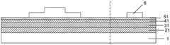
- FIG. 1shows a cross-sectional view of an array substrate provided with a non-photosensitive resin structure, as shown in FIG.
- the substrateis divided into a pixel area and a gate on array (GOA) region, which are respectively located on the left and right sides of the dotted line in the figure, and the two portions are simultaneously formed by multiple patterning processes
- the array substrateincludes: formed on the substrate a gate electrode 2 and a gate line in the display region, and a gate line lead of the array substrate row driving region; a gate insulating layer 3 formed over the gate electrode 2 and over the gate line covering the entire substrate 1; formed over the gate insulating layer 3
- the preparation of the structure as shown in FIG. 1requires eight patterning processes, that is, forming the gate electrode 2, the gate lines, and the gate line leads. a first patterning process, a second patterning process of forming the gate insulating layer 3, a third patterning process of forming the active layer 4 and the ohmic contact layer 5, a fourth patterning process of forming the source/drain electrodes 7 and their layers of metal, A fifth patterning process of forming the planarization layer 9, a sixth patterning process of forming the pixel electrode 10, a seventh patterning process of forming the first passivation layer 11, and an eighth patterning process of forming the common electrode 12 and its peer electrode. Therefore, a larger number of masks are required, which makes the preparation process more complicated and has lower productivity.
- Embodiments of the present inventionprovide an array substrate, a manufacturing method thereof, and a display device, which can reduce the number of mask plates in the preparation process and improve production efficiency.
- an embodiment of the present inventionprovides a method of fabricating an array substrate, comprising: preparing a substrate including a pixel region and an array substrate row driving region; and the substrate is processed by a first patterning process Forming a pattern including a gate and a pattern of an active layer, and forming a gate lead in the row driving region of the array substrate; forming a pattern of the gate insulating layer by a second patterning process; forming a source drain through the third patterning process a pattern of the pole; a pattern of the planarization layer formed by the fourth patterning process; and a pattern including the pixel electrode is formed by the fifth patterning process.
- an embodiment of the present inventionfurther provides an array substrate, including: a substrate substrate including a pixel region and an array substrate row driving region; a pattern and a gate including a gate formed sequentially on the substrate substrate A pattern of an insulating layer, a pattern of an active layer, a pattern including a source and a drain, a pattern of a planarization layer, and a pattern including a pixel electrode.
- an embodiment of the inventionfurther provides a display device comprising the array substrate of any of the above.
- FIG. 1is a schematic cross-sectional structural view of a conventional resin-containing array substrate
- FIG. 2is a cross-sectional structural view showing a method of fabricating a gate metal film, a first gate insulating layer film, an active layer film, and an ohmic contact layer film on a substrate substrate in a method of fabricating an array substrate according to an embodiment of the invention
- FIG. 3is a cross-sectional structural view showing a photosensitive material after exposure and development using a halftone mask in a method of fabricating an array substrate according to an embodiment of the present invention
- FIG. 4is a cross-sectional structural view showing a pattern including a gate electrode in a method of fabricating an array substrate according to an embodiment of the present invention
- FIG. 5is a cross-sectional structural view showing a method of manufacturing an array substrate in accordance with an embodiment of the present invention
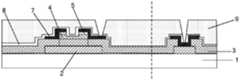
- FIG. 6is a cross-sectional structural view of an array substrate obtained by etching after ashing in a method of fabricating an array substrate according to an embodiment of the invention
- FIG. 7is a cross-sectional structural view showing a second gate insulating film deposited in a method of fabricating an array substrate according to an embodiment of the invention.
- FIG. 8is a cross-sectional structural view showing a pattern of an active layer formed in a method of fabricating an array substrate according to an embodiment of the present invention
- FIG. 9is a cross-sectional structural view showing a pattern of forming a gate insulating layer in a method of fabricating an array substrate according to an embodiment of the present invention.
- FIG. 10is a cross-sectional structural view showing a pattern and a channel including a source and a drain in a method of fabricating an array substrate according to an embodiment of the present invention
- FIG. 11is a cross-sectional structural view showing a pattern of a planarization layer in a method of fabricating an array substrate according to an embodiment of the present invention
- FIG. 12is a cross-sectional structural view showing a pattern including a pixel electrode in a method of fabricating an array substrate according to an embodiment of the present invention
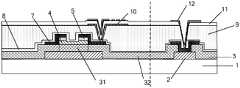
- Figure 13is a schematic cross-sectional view showing an array substrate containing a resin according to an embodiment of the present invention.
- the gate and the active layerare simultaneously formed by one patterning process, thereby reducing the number of masks and improving production efficiency. ,cut costs.
- the patterning processrefers to a process of forming a pattern including photoresist or photosensitive material coating, exposure, development, etching, photoresist, or photosensitive material peeling.
- the process of forming a pattern in the embodiment of the present inventionmay also employ other processes such as printing for patterning.
- Photoresist or photosensitive materialis a kind of light-sensitive substance, taking photoresist as an example, according to its chemistry
- the reaction mechanism and the development principlecan be divided into two types: negative gel and positive gel.
- Negative glueis formed after the formation of insoluble matter after illumination; on the contrary, it is insoluble to some solvents, and it is a positive glue after being irradiated to become a soluble substance.
- the embodiment of the present inventionis described by taking a positive photoresist as an example, that is, it is insoluble to the developer, and becomes a soluble substance after exposure to expose the structure on the substrate.
- a photoresist complete removal regionis formed on the substrate through the light-transmitting region of the mask, and a photoresist completely reserved region is formed on the substrate through the opaque region of the mask, through the mask
- the semi-transmissive regionforms a photoresist semi-reserved region on the substrate.
- the left side of the dotted line in each drawingis the pixel area of the array substrate, and the right side of the dotted line is the array substrate row driving area, that is, the peripheral lead area forming the circuit.
- a method of manufacturing an array substrate according to an embodiment of the present inventionincludes:
- Step 201preparing a substrate including a pixel region and an array substrate row driving region
- Step 202forming a pattern including a gate and a pattern of an active layer on a base substrate by a first patterning process, and forming a gate lead in the GOA region;
- a pattern including the gate and a pattern of an active layerare formed on the base substrate by a first patterning process using a halftone mask and a ground lift-off process, the halftone mask being active and active.
- the area corresponding to the pattern of the layeris opaque, and the area corresponding to the gate in the pixel area and the area corresponding to the gate lead in the GOA area are partially transparent, and the remaining area is completely transparent.
- step 202includes:
- a gate metal layer film, a first gate insulating layer film, and an active layer filmare sequentially formed on a base substrate.
- the photosensitive materialis exposed and developed using a halftone mask, a photosensitive material completely remaining region is formed in a region corresponding to the pattern of the active layer, and a photosensitive material semi-retained region is formed in a region corresponding to the pattern including the gate electrode, The remaining area forms a complete removal area of the photosensitive material;
- the positive photoresistis exposed and developed by using a halftone mask mask, and the area of the halftone mask corresponding to the pattern of the active layer is opaque, The positive photoresist at the place is completely retained; the area of the halftone mask corresponding to the pattern including the gate is semi-transmissive, where the positive photoresist is semi-retained; the halftone mask corresponds to the substrate The rest of the area is completely transparent, The positive photoresist here will be completely removed.
- the active layer film, the first gate insulating layer film, and the gate metal layer film of the photosensitive material completely removed regionare removed by the first etching;
- the ashing treatment of the photosensitive materialis performed to remove the photosensitive material in the semi-retained area of the photosensitive material, and the active layer film and the first gate insulating layer film of the semi-reserved region of the photosensitive material are removed by the second etching to obtain a gate including the gate.
- the second gate insulating layer film and the photosensitive material in the completely remaining region of the photosensitive materialare removed by a ground stripping process to obtain a pattern of the active layer.
- Step 203forming a pattern of a gate insulating layer on a substrate formed with a pattern including a gate and a pattern of an active layer by a second patterning process;
- Step 204forming a pattern including a source and a drain on a substrate formed with a pattern of a gate insulating layer by a third patterning process;
- Step 205forming a pattern of the planarization layer on the substrate forming the pattern of the active drain by the fourth patterning process;
- Step 206sequentially forming a pattern including a pixel electrode, a pattern of the first passivation layer, and a pattern of the common electrode on the substrate on which the pattern of the planarization layer is formed by a patterning process.
- the thickness of the first gate insulating layer filmis equal to the thickness of the second gate insulating layer film such that the pattern of the gate insulating layer formed has no end difference.
- the method of fabricating an array substrate according to an embodiment of the present inventionfurther includes forming a pattern of an ohmic contact layer after forming a pattern of the active layer.
- the pattern forming the ohmic contact layerincludes:
- Forming the same pattern as the active layerthat is, a pre-pattern of the pattern of the conformal ohmic contact layer, using a first patterning process while forming a pattern of the active layer;
- a pattern of the ohmic contact layeris formed by etching a pre-pattern of the pattern of the ohmic contact layer while forming the pattern including the source and drain electrodes.
- Figures 2-11show the formation of ohms after forming the pattern of the active layer.
- An example of the pattern of the contact layerthat is, an ohmic contact layer film is also formed on the active layer film, but if it is not necessary to form the pattern of the ohmic contact layer, it is not necessary to form an ohmic contact layer film on the active layer film.
- the corresponding drawingsare not given here, and the embodiment of the present invention does not limit this.
- step 202includes:
- a gate metal layer film 21is deposited on the base substrate 1, and the gate metal layer film may be a metal material such as aluminum, copper, chromium or molybdenum, or an alloy thereof. Then, a first gate insulating layer film 31 is sequentially deposited on the gate metal layer film 21, exemplarily, may be formed of SiN x , and an active layer film 41, as shown in FIG. 2, and in an active layer film Forming an ohmic contact layer film 51 on 41;
- a photosensitive material 6such as a photoresist or a photosensitive resin is coated on the ohmic contact layer film 51, and the photosensitive material is exposed and developed by a halftone mask, in a pattern corresponding to the active layer and ohmic contact.
- the patterned region of the layerforms a completely retained region of the photosensitive material, the photosensitive material semi-retained region is formed in a region corresponding to the pattern including the gate electrode, and the remaining region forms a photosensitive material completely removed region;
- the photosensitive materialis exposed and developed by using a halftone mask, and a region of the halftone mask corresponding to the pattern of the active layer and the pattern of the ohmic contact layer is opaque, The positive photoresist at the place is completely retained; the area of the halftone mask corresponding to the pattern including the gate is semi-transmissive, where the positive photoresist is semi-retained; the halftone mask corresponds to the substrate The rest of the area is completely transparent, and the positive photoresist here will be completely removed;
- the region of the halftone mask corresponding to the pattern 4 of the active layer to be formedis opaque, the region corresponding to the gate region 2 of the pixel region to be formed, and the gate of the GOA region
- the regions corresponding to the leadsare partially transparent, and the remaining regions are completely transparent.
- the photoresist or the photosensitive resinis exposed and developed by using the halftone mask, and then the structure shown in FIG. 3 is obtained;
- etchingis performed to remove the gate metal layer film 21, the first gate insulating layer film 31, the active layer film 41, and the ohmic contact layer film 51 in the region where the photosensitive material (photoresist or photosensitive resin) is completely removed by one etching.
- an ashing treatment of the photosensitive materialis performed to remove the photosensitive material in the semi-retained area of the photosensitive material to obtain a structure as shown in FIG. 5; then a second etching is performed to remove the photosensitive
- the ohmic contact layer film 51 of the material semi-retained region, the active layer film 41 and the first gate insulating layer film 31are obtained as a pattern including the gate electrode 2, as shown in FIG. 6;
- the second gate insulating layer film 32is removed from the second gate insulating layer film and the photosensitive material on the completely remaining region of the photosensitive material by a ground lift-off process to obtain a pattern of the active layer.
- the photoresist or the photosensitive resin on the active layer film 4is left, and deposition is continued by plasma enhanced chemical vapor deposition (PECVD).
- PECVDplasma enhanced chemical vapor deposition
- the second gate insulating film 32 of the entire substrateis obtained as shown in FIG. 7, wherein the thickness of the second gate insulating film 32 is the same as the thickness of the first gate insulating film 31 shown in FIG.
- the ground stripping techniquethe second gate insulating layer film and the photosensitive material (photoresist or photosensitive resin) on the completely remaining region of the photosensitive material are removed to obtain the pattern 4 of the active layer, as shown in FIG.
- a pre-pattern of the pattern of the ohmic contact layeris formed and formed in the same pattern as the active layer, that is, conformal.
- the pattern 5 of the ohmic contact layeris formed by etching away the ohmic contact layer film 51 of the channel region when the pattern of the source and drain electrodes is subsequently formed.
- the metal layer of the source drain region and the GOA regionis first etched away by wet etching, and then the ohmic contact layer film 51 at the channel region is etched away by dry etching.
- a pattern including a source drain and a pattern of an ohmic contact layerare formed.
- this steponly forms a gate electrode and an active layer by using one mask process by using one mask process of a halftone mask, which saves a mask plate compared with the prior art, saves cost and improves the cost. Productivity.
- step 203includes:
- the deposited second gate insulating layer film 32is patterned, that is, exposed and developed through a mask, and etched to form a gate insulating film.
- step 204includes:
- Exposing and developing the photosensitive material with the maskforming a complete removal region of the photosensitive material corresponding to the gate lead in a region corresponding to the channel region and the row driving region of the array substrate;
- the methodfurther includes: forming a pattern of the second passivation layer 8 on the substrate forming the pattern of the active drain, comprising:
- a pattern 8 of a second passivation layeris formed, the pattern of the second passivation layer 8 covering the entire substrate, that is, formed on the pattern 3 of the gate insulating layer, over the pattern including the source and drain electrodes.
- the pattern 8 of the second passivation layeris formed to prevent the organic resin solvent component contained in the overflow gas from infiltrating into the active layer when the subsequent planarization layer is heated, so that surface defects of the active layer are increased, and the TFT is affected.
- step 205forming a pattern of the planarization layer on the base substrate formed with the pattern including the source and drain, comprising:
- a resin materialsuch as an organic resin, is formed on the base substrate on which the pattern 7 including the source and drain electrodes is formed, and a pattern 9 of the planarization layer is formed by a patterning process, and a via hole is formed in the corresponding pixel region and the GOA region, as shown in FIG. 11 is shown.
- the thickness of the planarization layer 9is 1.8 to 2.5 ⁇ m.
- step 206: sequentially forming a pattern of the pixel electrode, a pattern of the first passivation layer, and a pattern of the common electrode on the base substrate on which the pattern of the planarization layer is formedincludes:
- ITOindium tin oxide
- the preparation of the gate electrode and the active layer in the embodiment of the present inventionrequires only one piece in comparison with the prior art in which each of the gate electrode and the active layer is prepared by a mask.
- the mask platereduces the number of mask processes, effectively saves costs and improves production efficiency.
- the embodiment of the present inventionfurther provides an array substrate, which is fabricated by the above method, and has a structure as shown in FIG. 13 , including: a pattern including a gate electrode 2 formed on the substrate 1 ; a pattern 3 covering the gate insulating layer of the entire base substrate 1 on the pattern including the gate 2; a pattern 4 of the active layer formed on the pattern 3 of the gate insulating layer; and a source formed on the pattern 3 of the gate insulating layer a pattern 7 of the drain, the pattern 7 including the source and drain of the GOA region is connected to the gate lead through a via in the pattern 3 of the gate insulating layer; a pattern formed on the pattern 7 including the source and drain and the gate insulating layer a pattern 9 of a planarization layer on 3; a pattern 10 of pixel electrodes formed on the pattern 9 of the planarization layer by a via in the pattern 9 of the planarization layer and a pattern 7 including a source and drain;
- the pattern of the pole 2 and the pattern 4 of the active layerare
- the pattern 3 of the gate insulating layerincludes the pattern 31 of the first gate insulating layer formed of the first gate insulating layer film and the pattern of the second gate insulating layer formed of the second gate insulating layer film 32; in the GOA region, the pattern 3 of the gate insulating layer is formed by the second gate insulating layer film 32, and the first gate insulating layer film and the second gate insulating layer film have the same thickness, and the first gate insulating The pattern 31 of the layer is conformal to the pattern 4 of the active layer.
- the array substratefurther includes a pattern 5 of an ohmic contact layer formed over the pattern 4 of the active layer and under the pattern 7 including the source and drain electrodes.
- the array substratefurther includes a pattern of the first passivation layer 8 formed over the pattern 7 including the source and drain and below the planarization layer 9.
- the array substratefurther includes: a pattern 11 of a second passivation layer formed over the pattern 10 including the pixel electrode, as shown in FIG. 13, and a common electrode formed over the pattern 11 of the second passivation layer Pattern 12.
- Embodiments of the present inventionalso provide a display device including the array substrate as described above.
- An embodiment of the present inventionprovides an array substrate, a method of fabricating the same, and a display device, wherein the gate and the active layer are formed on a substrate by a patterning process using a halftone mask.
- the prior art gate and active layereach require a mask, and in the embodiment of the invention, only a mask is needed for the preparation of the gate and the active layer, which reduces the patterning process. The number of times, effectively saving costs and improving production efficiency.
Landscapes
- Physics & Mathematics (AREA)
- Nonlinear Science (AREA)
- Engineering & Computer Science (AREA)
- Microelectronics & Electronic Packaging (AREA)
- Mathematical Physics (AREA)
- Chemical & Material Sciences (AREA)
- Crystallography & Structural Chemistry (AREA)
- General Physics & Mathematics (AREA)
- Optics & Photonics (AREA)
- Thin Film Transistor (AREA)
- Liquid Crystal (AREA)
Abstract
Description
Translated fromChinese本发明的实施例涉及一种阵列基板及其制作方法和显示装置。Embodiments of the present invention relate to an array substrate, a method of fabricating the same, and a display device.
薄膜晶体管液晶显示器(TFT-LCD)多年来一直受到人们的广泛关注。目前高分辨率、低功耗的TFT-LCD成为发展的重点和研发的热点。Thin film transistor liquid crystal displays (TFT-LCDs) have been receiving widespread attention for many years. At present, high-resolution, low-power TFT-LCD has become the focus of development and a hot spot for research and development.
高分辨率和低功耗的TFT-LCD需要形成低介电常数的非感光树脂结构,图1中示出了设有非感光树脂结构的阵列基板的截面图,如图1所示,该阵列基板分为像素区域和阵列基板行驱动(GOA,gate on array)区域,分别位于图中虚线的左侧和右侧,两部分由多次构图工艺同时形成,所述阵列基板包括:形成于基板1显示区域中的栅极2和栅线,以及阵列基板行驱动区域的栅线引线;形成于栅极2和栅线上方覆盖整个基板1的栅绝缘层3;形成于栅绝缘层3上方的有源层4;形成于有源层4上方的欧姆接触层5;形成于欧姆接触层5和栅绝缘层3上的源/漏极7,同时在所述阵列基板行驱动区域形成的源/漏极7的同层金属,通过栅绝缘层3中的过孔与栅极引线相连;形成于源/漏极7及其同层金属上方以及栅绝缘层3上的平坦化层9;形成于平坦化层9上通过平坦化层9中的过孔与源/漏极7相连的像素电极10;形成于平坦化层9和像素电极10上的第一钝化层11;形成于第一钝化层11上的公共电极12,以及在阵列基板行驱动区域通过钝化层过孔和平坦化层过孔与源/漏极7的同层金属相连的公共电极的同层电极。A high-resolution and low-power TFT-LCD requires a non-photosensitive resin structure having a low dielectric constant, and FIG. 1 shows a cross-sectional view of an array substrate provided with a non-photosensitive resin structure, as shown in FIG. The substrate is divided into a pixel area and a gate on array (GOA) region, which are respectively located on the left and right sides of the dotted line in the figure, and the two portions are simultaneously formed by multiple patterning processes, and the array substrate includes: formed on the substrate a
目前,由于制备平坦化层,因此需要的掩模的数量较多,通常如图1中所示的结构的制备共需要进行八次构图工艺,即:形成栅极2、栅线和栅线引线的第一构图工艺、形成栅绝缘层3的第二构图工艺、形成有源层4和欧姆接触层5的第三构图工艺、形成源/漏极7及其同层金属的第四构图工艺、形成平坦化层9的第五构图工艺、形成像素电极10的第六构图工艺、形成第一钝化层11的第七构图工艺、形成公共电极12及其同层电极的第八构图工艺。因此,需要较多数量的掩模,使得制备流程较复杂,且产能较低。At present, since the number of masks required is large due to the preparation of the planarization layer, generally, the preparation of the structure as shown in FIG. 1 requires eight patterning processes, that is, forming the
发明内容Summary of the invention
本发明的实施例提供一种阵列基板及其制作方法和显示装置,可减少制备过程中掩模板的数量,提高生产效率。Embodiments of the present invention provide an array substrate, a manufacturing method thereof, and a display device, which can reduce the number of mask plates in the preparation process and improve production efficiency.
一方面,本发明的实施例提供一种阵列基板的制作方法,包括:准备衬底基板,所述衬底基板包括像素区域和阵列基板行驱动区域;通过第一构图工艺在所述衬底基板上形成包括栅极的图案和有源层的图案,且在所述阵列基板行驱动区域形成栅极引线;通过第二构图工艺形成栅极绝缘层的图案;通过第三构图工艺形成包括源漏极的图案;通过第四构图工艺形成平坦化层的图案;以及通过第五构图工艺形成包括像素电极的图案。In one aspect, an embodiment of the present invention provides a method of fabricating an array substrate, comprising: preparing a substrate including a pixel region and an array substrate row driving region; and the substrate is processed by a first patterning process Forming a pattern including a gate and a pattern of an active layer, and forming a gate lead in the row driving region of the array substrate; forming a pattern of the gate insulating layer by a second patterning process; forming a source drain through the third patterning process a pattern of the pole; a pattern of the planarization layer formed by the fourth patterning process; and a pattern including the pixel electrode is formed by the fifth patterning process.
另一方面,本发明的实施例还提供一种阵列基板,包括:衬底基板,包括像素区域以及阵列基板行驱动区域;在所述衬底基板上顺次形成的包括栅极的图案、栅绝缘层的图案、有源层的图案、包括源漏极的图案、平坦化层的图案、包括像素电极的图案。In another aspect, an embodiment of the present invention further provides an array substrate, including: a substrate substrate including a pixel region and an array substrate row driving region; a pattern and a gate including a gate formed sequentially on the substrate substrate A pattern of an insulating layer, a pattern of an active layer, a pattern including a source and a drain, a pattern of a planarization layer, and a pattern including a pixel electrode.
再一方面,本发明的实施例还提供一种显示装置,包括上述任一项所述的阵列基板。In a further aspect, an embodiment of the invention further provides a display device comprising the array substrate of any of the above.
为了更清楚地说明本发明实施例的技术方案,下面将对实施例的附图作简单地介绍,显而易见地,下面描述中的附图仅仅涉及本发明的一些实施例,而非对本发明的限制。In order to more clearly illustrate the technical solutions of the embodiments of the present invention, the drawings of the embodiments will be briefly described below. It is obvious that the drawings in the following description relate only to some embodiments of the present invention, and are not intended to limit the present invention. .
图1为现有的含有树脂的阵列基板的剖面结构示意图;1 is a schematic cross-sectional structural view of a conventional resin-containing array substrate;
图2为根据本发明实施例的阵列基板的制造方法中在衬底基板上沉积栅极金属薄膜、第一栅绝缘层薄膜、有源层薄膜以及欧姆接触层薄膜后的截面结构图;2 is a cross-sectional structural view showing a method of fabricating a gate metal film, a first gate insulating layer film, an active layer film, and an ohmic contact layer film on a substrate substrate in a method of fabricating an array substrate according to an embodiment of the invention;
图3为根据本发明实施例的阵列基板的制造方法中采用半色调掩模对感光材料进行曝光显影后的截面结构图;3 is a cross-sectional structural view showing a photosensitive material after exposure and development using a halftone mask in a method of fabricating an array substrate according to an embodiment of the present invention;
图4为根据本发明实施例的阵列基板的制造方法中形成包括栅极的图案后的截面结构图;4 is a cross-sectional structural view showing a pattern including a gate electrode in a method of fabricating an array substrate according to an embodiment of the present invention;
图5为根据本发明实施例的阵列基板的制造方法中对感光材料进行灰化处理后的截面结构图;5 is a cross-sectional structural view showing a method of manufacturing an array substrate in accordance with an embodiment of the present invention;
图6为根据本发明实施例的阵列基板的制造方法中灰化处理后进行刻蚀得到的阵列基板的截面结构图;6 is a cross-sectional structural view of an array substrate obtained by etching after ashing in a method of fabricating an array substrate according to an embodiment of the invention;
图7为根据本发明实施例的阵列基板的制造方法中沉积第二栅绝缘层薄膜后的截面结构图;7 is a cross-sectional structural view showing a second gate insulating film deposited in a method of fabricating an array substrate according to an embodiment of the invention;
图8为根据本发明实施例的阵列基板的制造方法中形成有源层的图案后的截面结构图;8 is a cross-sectional structural view showing a pattern of an active layer formed in a method of fabricating an array substrate according to an embodiment of the present invention;
图9为根据本发明实施例的阵列基板的制造方法中形成栅绝缘层的图案后的截面结构图;9 is a cross-sectional structural view showing a pattern of forming a gate insulating layer in a method of fabricating an array substrate according to an embodiment of the present invention;
图10为根据本发明实施例的阵列基板的制造方法中形成包括源漏极的图案和沟道后的截面结构图;10 is a cross-sectional structural view showing a pattern and a channel including a source and a drain in a method of fabricating an array substrate according to an embodiment of the present invention;
图11为根据本发明实施例的阵列基板的制造方法中形成平坦化层的图案后的截面结构图;11 is a cross-sectional structural view showing a pattern of a planarization layer in a method of fabricating an array substrate according to an embodiment of the present invention;
图12为根据本发明实施例的阵列基板的制造方法中形成包括像素电极的图案后的截面结构图;以及12 is a cross-sectional structural view showing a pattern including a pixel electrode in a method of fabricating an array substrate according to an embodiment of the present invention;
图13为根据本发明实施例的含有树脂的阵列基板的剖面结构示意图。Figure 13 is a schematic cross-sectional view showing an array substrate containing a resin according to an embodiment of the present invention.
为使本发明实施例的目的、技术方案和优点更加清楚,下面将结合本发明实施例的附图,对本发明实施例的技术方案进行清楚、完整地描述。显然,所描述的实施例是本发明的一部分实施例,而不是全部的实施例。基于所描述的本发明的实施例,本领域普通技术人员在无需创造性劳动的前提下所获得的所有其他实施例,都属于本发明保护的范围。The technical solutions of the embodiments of the present invention will be clearly and completely described in the following with reference to the accompanying drawings. It is apparent that the described embodiments are part of the embodiments of the invention, and not all of the embodiments. All other embodiments obtained by a person of ordinary skill in the art based on the described embodiments of the present invention without departing from the scope of the invention are within the scope of the invention.
本发明的实施例中,采用半色调掩膜(Half tone mask)和离地剥离(lift off)技术,通过一次构图工艺同时形成栅极和有源层,可减少掩模板的数量,提高生产效率,降低成本。In the embodiment of the present invention, by using a half tone mask and a lift off technique, the gate and the active layer are simultaneously formed by one patterning process, thereby reducing the number of masks and improving production efficiency. ,cut costs.
示例性地,应该理解,在本发明的实施例中,构图工艺是指包括光刻胶或感光材料涂敷、曝光、显影、蚀刻、光刻胶或感光材料剥离等形成图案的工艺。当然,本发明实施例中形成图案的工艺还可以采用如打印等其他用用于构图的工艺。Illustratively, it should be understood that in the embodiment of the present invention, the patterning process refers to a process of forming a pattern including photoresist or photosensitive material coating, exposure, development, etching, photoresist, or photosensitive material peeling. Of course, the process of forming a pattern in the embodiment of the present invention may also employ other processes such as printing for patterning.
光刻胶或感光材料是一类对光敏感的物质,以光刻胶为例,根据其化学反应机理和显影原理,可分负性胶和正性胶两类。光照后形成不可溶物质的是负性胶;反之,对某些溶剂是不可溶的,经光照后变成可溶物质的即为正性胶。本发明实施例以正性光刻胶为例进行说明,即其本身对显影液是不可溶的,经曝光以后变成可溶物质从而暴露基板上的结构。相应的,本发明的实施例中,通过掩模板的透光区域在基板上形成光刻胶完全去除区,通过掩模板的不透光区域在基板上形成光刻胶完全保留区,通过掩模板的半透光区域在基板上形成光刻胶半保留区。Photoresist or photosensitive material is a kind of light-sensitive substance, taking photoresist as an example, according to its chemistryThe reaction mechanism and the development principle can be divided into two types: negative gel and positive gel. Negative glue is formed after the formation of insoluble matter after illumination; on the contrary, it is insoluble to some solvents, and it is a positive glue after being irradiated to become a soluble substance. The embodiment of the present invention is described by taking a positive photoresist as an example, that is, it is insoluble to the developer, and becomes a soluble substance after exposure to expose the structure on the substrate. Correspondingly, in the embodiment of the present invention, a photoresist complete removal region is formed on the substrate through the light-transmitting region of the mask, and a photoresist completely reserved region is formed on the substrate through the opaque region of the mask, through the mask The semi-transmissive region forms a photoresist semi-reserved region on the substrate.
下面结合附图对本发明的实施例进行详细说明。其中,各附图中虚线左侧区域为阵列基板的像素区域,虚线右侧为阵列基板行驱动区域,即形成电路的周边引线区域。The embodiments of the present invention will be described in detail below with reference to the accompanying drawings. The left side of the dotted line in each drawing is the pixel area of the array substrate, and the right side of the dotted line is the array substrate row driving area, that is, the peripheral lead area forming the circuit.
示例性地,根据本发明实施例的阵列基板的制造方法,包括:Illustratively, a method of manufacturing an array substrate according to an embodiment of the present invention includes:
步骤201:准备衬底基板,该衬底基板包括像素区域和阵列基板行驱动区域;Step 201: preparing a substrate including a pixel region and an array substrate row driving region;
步骤202:通过第一构图工艺在衬底基板上形成包括栅极的图案和有源层的图案,且在所述GOA区域中形成栅极引线;Step 202: forming a pattern including a gate and a pattern of an active layer on a base substrate by a first patterning process, and forming a gate lead in the GOA region;
本步骤中,通过采用半色调掩模和离地剥离工艺的第一构图工艺在衬底基板上形成包括所述栅极的图案和有源层的图案,所述半色调掩模中与有源层的图案对应的区域不透光,与像素区域中栅极对应的区域以及与GOA区域中栅极引线对应的区域均部分透光,剩余的区域全透光。In this step, a pattern including the gate and a pattern of an active layer are formed on the base substrate by a first patterning process using a halftone mask and a ground lift-off process, the halftone mask being active and active The area corresponding to the pattern of the layer is opaque, and the area corresponding to the gate in the pixel area and the area corresponding to the gate lead in the GOA area are partially transparent, and the remaining area is completely transparent.
示例性地,步骤202包括:Illustratively, step 202 includes:
首先,在衬底基板上顺序形成栅金属层薄膜、第一栅绝缘层薄膜、以及有源层薄膜。First, a gate metal layer film, a first gate insulating layer film, and an active layer film are sequentially formed on a base substrate.
然后,在所述有源层薄膜上涂覆感光材料。Then, a photosensitive material is coated on the active layer film.
再次,利用半色调掩模对所述感光材料进行曝光显影,在对应于有源层的图案的区域形成感光材料完全保留区,在对应于包括栅极的图案的区域形成感光材料半保留区,其余区域形成感光材料完全去除区;Again, the photosensitive material is exposed and developed using a halftone mask, a photosensitive material completely remaining region is formed in a region corresponding to the pattern of the active layer, and a photosensitive material semi-retained region is formed in a region corresponding to the pattern including the gate electrode, The remaining area forms a complete removal area of the photosensitive material;
示例性地,以正性光刻胶为例,利用半色调掩膜版掩模对正性光刻胶进行曝光显影,半色调掩模的对应于有源层的图案的区域不透光,此处的正性光刻胶完全保留;半色调掩模的对应于包括栅极的图案的区域半透光,此处的正性光刻胶半保留;半色调掩模的对应于衬底基板的其余区域完全透光,此处的正性光刻胶将被完全去除。Illustratively, with a positive photoresist as an example, the positive photoresist is exposed and developed by using a halftone mask mask, and the area of the halftone mask corresponding to the pattern of the active layer is opaque, The positive photoresist at the place is completely retained; the area of the halftone mask corresponding to the pattern including the gate is semi-transmissive, where the positive photoresist is semi-retained; the halftone mask corresponds to the substrate The rest of the area is completely transparent,The positive photoresist here will be completely removed.
再次,通过第一次刻蚀去除感光材料完全去除区的有源层薄膜、第一栅绝缘层薄膜以及栅金属层薄膜;Again, the active layer film, the first gate insulating layer film, and the gate metal layer film of the photosensitive material completely removed region are removed by the first etching;
再次,进行感光材料的灰化处理,去除感光材料半保留区的感光材料,并通过第二次刻蚀,去除感光材料半保留区的有源层薄膜和第一栅绝缘层薄膜,得到包括栅极的图案;Again, the ashing treatment of the photosensitive material is performed to remove the photosensitive material in the semi-retained area of the photosensitive material, and the active layer film and the first gate insulating layer film of the semi-reserved region of the photosensitive material are removed by the second etching to obtain a gate including the gate. Extreme pattern
再次,采用形成所述第一栅绝缘层薄膜的材料形成覆盖整个衬底基板的第二栅绝缘层薄膜;And forming a second gate insulating layer film covering the entire substrate by using a material forming the first gate insulating film;
最后,采用离地剥离工艺去除所述感光材料完全保留区中的第二栅绝缘层薄膜和感光材料,得到有源层的图案。Finally, the second gate insulating layer film and the photosensitive material in the completely remaining region of the photosensitive material are removed by a ground stripping process to obtain a pattern of the active layer.
步骤203:通过第二构图工艺在形成有包括栅极的图案和有源层的图案的衬底基板上形成栅绝缘层的图案;Step 203: forming a pattern of a gate insulating layer on a substrate formed with a pattern including a gate and a pattern of an active layer by a second patterning process;
步骤204:通过第三构图工艺在形成有栅绝缘层的图案的衬底基板上形成包括源漏极的图案;Step 204: forming a pattern including a source and a drain on a substrate formed with a pattern of a gate insulating layer by a third patterning process;
步骤205:通过第四构图工艺在形成有源漏极的图案的基板上形成平坦化层的图案;Step 205: forming a pattern of the planarization layer on the substrate forming the pattern of the active drain by the fourth patterning process;
步骤206:通过构图工艺在形成有平坦化层的图案的基板上顺序形成包括像素电极的图案、第一钝化层的图案和公共电极的图案。Step 206: sequentially forming a pattern including a pixel electrode, a pattern of the first passivation layer, and a pattern of the common electrode on the substrate on which the pattern of the planarization layer is formed by a patterning process.
示例性地,第一栅绝缘层薄膜的厚度等于第二栅绝缘层薄膜的厚度,以使得所形成的栅绝缘层的图案没有端差。Illustratively, the thickness of the first gate insulating layer film is equal to the thickness of the second gate insulating layer film such that the pattern of the gate insulating layer formed has no end difference.
示例性地,根据本发明实施例的阵列基板的制造方法还包括:在形成有源层的图案之后,形成欧姆接触层的图案。Illustratively, the method of fabricating an array substrate according to an embodiment of the present invention further includes forming a pattern of an ohmic contact layer after forming a pattern of the active layer.
示例性地,形成欧姆接触层的图案包括:Illustratively, the pattern forming the ohmic contact layer includes:
与形成有源层的图案同时采用第一构图工艺形成与有源层的图案一样,即,共形的所述欧姆接触层的图案的预图案;以及Forming the same pattern as the active layer, that is, a pre-pattern of the pattern of the conformal ohmic contact layer, using a first patterning process while forming a pattern of the active layer;
与形成所述包括源漏极的图案的同时,蚀刻所述欧姆接触层的图案的预图案而形成所述欧姆接触层的图案。A pattern of the ohmic contact layer is formed by etching a pre-pattern of the pattern of the ohmic contact layer while forming the pattern including the source and drain electrodes.
下面,结合附图2-11对根据本发明实施例的阵列基板的制造方法的步骤进行详述。Hereinafter, the steps of the method of fabricating the array substrate according to the embodiment of the present invention will be described in detail with reference to FIGS. 2-11.
这里应该注意的是,附图2-11给出的是形成有源层的图案之后形成欧姆接触层的图案的示例,也就是,在有源层薄膜上还形成有欧姆接触层薄膜,但是如果不需要形成欧姆接触层的图案,则不需要在有源层薄膜上形成欧姆接触层薄膜,这里没有给出对应的附图,本发明的实施例对此不做任何限定。It should be noted here that Figures 2-11 show the formation of ohms after forming the pattern of the active layer.An example of the pattern of the contact layer, that is, an ohmic contact layer film is also formed on the active layer film, but if it is not necessary to form the pattern of the ohmic contact layer, it is not necessary to form an ohmic contact layer film on the active layer film. The corresponding drawings are not given here, and the embodiment of the present invention does not limit this.
示例性地,步骤202包括:Illustratively, step 202 includes:
在衬底基板1上沉积栅金属层薄膜21,所述栅金属层薄膜可采用铝、铜、铬或钼等金属材料、或其合金。然后,在所述栅金属层薄膜21上顺序沉积第一栅绝缘层薄膜31,示例性地,可以由SiNx形成,以及有源层薄膜41,如图2所示,并且在有源层薄膜41上形成欧姆接触层薄膜51;A gate
之后,在所述欧姆接触层薄膜51上涂覆光刻胶或感光树脂等感光材料6,利用半色调掩模对所述感光材料进行曝光以及显影,在对应于有源层的图案和欧姆接触层的图案的区域形成感光材料完全保留区,在对应于包括栅极的图案的区域形成感光材料半保留区,其余区域形成感光材料完全去除区;Thereafter, a
这里,以正性光刻胶为例,利用半色调掩模板对所述感光材料进行曝光显影,半色调掩模的对应于有源层的图案和欧姆接触层的图案的区域不透光,此处的正性光刻胶完全保留;半色调掩模的对应于包括栅极的图案的区域半透光,此处的正性光刻胶半保留;半色调掩模的对应于衬底基板的其余区域完全透光,此处的正性光刻胶将被完全去除;Here, taking a positive photoresist as an example, the photosensitive material is exposed and developed by using a halftone mask, and a region of the halftone mask corresponding to the pattern of the active layer and the pattern of the ohmic contact layer is opaque, The positive photoresist at the place is completely retained; the area of the halftone mask corresponding to the pattern including the gate is semi-transmissive, where the positive photoresist is semi-retained; the halftone mask corresponds to the substrate The rest of the area is completely transparent, and the positive photoresist here will be completely removed;
之后,采用半色调掩模,所述半色调掩模的与待形成的有源层的图案4对应的区域不透光,与待形成的像素区域栅极2对应的区域以及与GOA区域栅极引线对应的区域均部分透光,剩余的区域全透光,采用所述半色调掩模板对所述光刻胶或感光树脂进行曝光显影,之后得到如图3所示的结构;Thereafter, a halftone mask is used, the region of the halftone mask corresponding to the
然后进行刻蚀,通过一次刻蚀去除感光材料(光刻胶或感光树脂)完全去除区域的栅金属层薄膜21、第一栅绝缘层薄膜31、有源层薄膜41,以及欧姆接触层薄膜51,形成图4所示的结构,即:与半色调掩模板的透光区域对应的区域被完全刻蚀掉;Then, etching is performed to remove the gate
接着,进行感光材料(光刻胶或感光树脂)的灰化(Ashing)处理,去除感光材料半保留区的感光材料,得到如图5所示的结构;然后进行第二次刻蚀,去除感光材料半保留区的欧姆接触层薄膜51、有源层薄膜41和第一栅绝缘层薄膜31,得到包括栅极2的图案,如图6所示;Next, an ashing treatment of the photosensitive material (photoresist or photosensitive resin) is performed to remove the photosensitive material in the semi-retained area of the photosensitive material to obtain a structure as shown in FIG. 5; then a second etching is performed to remove the photosensitive The ohmic
之后,采用与第一栅绝缘层薄膜相同的材料再形成一层覆盖整个基板的第二栅绝缘层薄膜32,并采用离地剥离工艺去除所述感光材料完全保留区上的第二栅绝缘层薄膜和感光材料,得到有源层的图案。Thereafter, a material similar to the first gate insulating film is used to form a layer covering the entire substrate.The second gate insulating
示例性地,这里,不进行光刻胶或感光树脂的剥离,即:保留有源层薄膜4上的光刻胶或感光树脂,利用等离子体增强化学气相沉积法(PECVD)继续沉积一层覆盖整个基板的第二栅绝缘层薄膜32,得到图7所示的结构,其中,该第二栅绝缘层薄膜32的厚度与图2中所示的第一栅绝缘层薄膜31的厚度相同,再利用离地剥离技术,除掉所述感光材料完全保留区上的第二栅绝缘层薄膜和感光材料(光刻胶或感光树脂),得到有源层的图案4,如图8所示。Illustratively, here, no peeling of the photoresist or the photosensitive resin is performed, that is, the photoresist or the photosensitive resin on the
此时欧姆接触层的图案的预图案被形成,且与有源层的图案形成为相同,即,共形。对于欧姆接触层的图案的预图案,在后续形成源漏极的图案时,通过刻蚀去除沟道区的欧姆接触层薄膜51而形成欧姆接触层的图案5。示例性地,在后续蚀刻源漏极薄膜时,先通过湿法刻蚀刻掉除源漏极区域和GOA区域的金属层,再通过干法刻蚀刻掉沟道区处的欧姆接触层薄膜51而形成包括源漏极的图案以及欧姆接触层的图案。At this time, a pre-pattern of the pattern of the ohmic contact layer is formed and formed in the same pattern as the active layer, that is, conformal. For the pre-pattern of the pattern of the ohmic contact layer, the
可见,本步骤仅通过采用半色调掩模的一次构图工艺,采用一块掩模板就同时形成了栅极与有源层,与现有技术相比,节省了一块掩模板,节省了成本,提高了生产效率。It can be seen that this step only forms a gate electrode and an active layer by using one mask process by using one mask process of a halftone mask, which saves a mask plate compared with the prior art, saves cost and improves the cost. Productivity.
示例性地,步骤203包括:Illustratively, step 203 includes:
在形成包括栅极2的图案和有源层的图案4的衬底基板上,对已沉积的第二栅绝缘层薄膜32进行图案化,即通过掩模板进行曝光显影、刻蚀,形成栅绝缘层的图案,其中包括过孔。其中,在所述栅绝缘层3与GOA区域的栅极引线对应的位置形成过孔,如图9所示。On the underlying substrate on which the
示例性地,步骤204包括:Illustratively, step 204 includes:
在形成有栅绝缘层的图案3的衬底基板上继续沉积源漏极金属薄膜;Depositing a source/drain metal film on the substrate of the
在所述源漏极金属薄膜上涂敷感光材料;Coating a photosensitive material on the source/drain metal film;
利用所述掩模对所述感光材料进行曝光以及显影,在对应于沟道区的区域以及在所述阵列基板行驱动区域对应于所述栅极引线形成所述感光材料完全去除区;Exposing and developing the photosensitive material with the mask, forming a complete removal region of the photosensitive material corresponding to the gate lead in a region corresponding to the channel region and the row driving region of the array substrate;
蚀刻所述感光材料完全去除区的所述源漏极金属薄膜以及欧姆接触层薄膜;Etching the source/drain metal film of the photosensitive material completely removed region and the ohmic contact layermembrane;
去除剩余的所述感光材料,形成所述源漏极的图案以所述欧姆接触层的图案,形成源漏极7和沟道,所述GOA区域形成的包括源漏极的图案通过栅绝缘层的图案3中的过孔与栅极引线相连,如图10所示。Removing the remaining photosensitive material, forming a pattern of the source and drain electrodes in a pattern of the ohmic contact layer, forming a source and a
示例性地,所述步骤204之后,该方法还包括:在形成有源漏极的图案的基板上形成第二钝化层8的图案,包括:Illustratively, after the step 204, the method further includes: forming a pattern of the second passivation layer 8 on the substrate forming the pattern of the active drain, comprising:
在衬底基板上继续沉积一层非金属材料,如氮化硅,厚度为
这里,所述第二钝化层的图案8形成的目的在于:防止后续平坦化层在加热时,溢出气体中含有的有机树脂溶剂成分渗入有源层,使有源层表面缺陷增多,影响TFT特性以及稳定性。Here, the pattern 8 of the second passivation layer is formed to prevent the organic resin solvent component contained in the overflow gas from infiltrating into the active layer when the subsequent planarization layer is heated, so that surface defects of the active layer are increased, and the TFT is affected. Features and stability.
示例性地,步骤205:在形成有包括源漏极的图案的衬底基板上形成平坦化层的图案,包括:Illustratively, step 205: forming a pattern of the planarization layer on the base substrate formed with the pattern including the source and drain, comprising:
在形成有包括源漏极的图案7的衬底基板上涂覆树脂材料,如有机树脂,并通过构图工艺形成平坦化层的图案9,对应像素区域以及GOA区域均形成有过孔,如图11所示。这里,所述平坦化层9的厚度为1.8~2.5μm。A resin material, such as an organic resin, is formed on the base substrate on which the
示例性地,步骤206:在形成有平坦化层的图案的衬底基板上顺序形成像素电极的图案、第一钝化层的图案和公共电极的图案,包括:Illustratively, step 206: sequentially forming a pattern of the pixel electrode, a pattern of the first passivation layer, and a pattern of the common electrode on the base substrate on which the pattern of the planarization layer is formed includes:
在形成有平坦化层的图案9的衬底基板上沉积一层透明导电材料薄膜,可选用氧化铟锡(ITO)等材料,并进行图案化形成像素电极的图案10,如图12所示;Depositing a transparent conductive material film on the substrate substrate on which the
在形成有像素电极的图案12的基板上沉积一层非金属薄膜,可选用SiNx等材料,并进行图形化,形成第一钝化层的图案11,所述第一钝化层的图案11中形成有过孔,如图12所示;Depositing a non-metal film on the substrate on which the
继续沉积一层透明导电材料薄膜,厚度为并进行图形化,形成公共电极的图案12,如图13所示。Continue to deposit a thin film of transparent conductive material with a thickness of And patterned to form a
从上述阵列基板的制作方法可以看出,与栅极和有源层的制备均各需要一块掩模板的现有技术相比,本发明的实施例中栅极和有源层的制备仅需要一块掩模板,较少了掩膜工艺的次数,有效节省了成本,提高了生产效率。As can be seen from the fabrication method of the above array substrate, the preparation of the gate electrode and the active layer in the embodiment of the present invention requires only one piece in comparison with the prior art in which each of the gate electrode and the active layer is prepared by a mask. The mask plate reduces the number of mask processes, effectively saves costs and improves production efficiency.
本发明实施例还提供了一种阵列基板,所述阵列基板是利用上述方法制作得到的,结构如图13所示,包括:形成于衬底基板1上的包括栅极2的图案;形成于包括栅极2的图案上覆盖整个衬底基板1的栅绝缘层的图案3;形成于栅绝缘层的图案3上的有源层的图案4;形成于栅绝缘层的图案3上的包括源漏极的图案7,所述GOA区域的包括源漏极的图案7通过栅绝缘层的图案3中的过孔与栅极引线相连;形成于包括源漏极的图案7和栅绝缘层的图案3上的平坦化层的图案9;形成于平坦化层的图案9上通过平坦化层的图案9中的过孔与包括源漏极的图案7相连的像素电极的图案10;所述包括栅极2的图案和有源层的图案4是由一次构图工艺形成的。The embodiment of the present invention further provides an array substrate, which is fabricated by the above method, and has a structure as shown in FIG. 13 , including: a pattern including a
示例性地,在像素区域中,栅绝缘层的图案3包括由第一栅绝缘层薄膜形成的第一栅绝缘层的图案31和由第二栅绝缘层薄膜形成的第二栅绝缘层的图案32;在GOA区域,栅绝缘层的图案3由所述第二栅绝缘层薄膜32形成,且所述第一栅绝缘层薄膜与所述第二栅绝缘层薄膜厚度相同,而且第一栅绝缘层的图案31与所述有源层的图案4共形。Illustratively, in the pixel region, the
示例性地,阵列基板还包括:形成在有源层的图案4上方以及包括源漏极的图案7下方的欧姆接触层的图案5。Illustratively, the array substrate further includes a
示例性地,阵列基板还包括:形成在包括源漏极的图案7上方且平坦化层9的下方形成的第一钝化层8的图案。Illustratively, the array substrate further includes a pattern of the first passivation layer 8 formed over the
示例性地,阵列基板还包括:形成在包括像素电极的图案10上方的第二钝化层的图案11,如图13所示,以及形成在第二钝化层的图案11上方的包括公共电极的图案12。Illustratively, the array substrate further includes: a
本发明的实施例还提供了一种显示装置,所述显示装置包括有如上所述的阵列基板。Embodiments of the present invention also provide a display device including the array substrate as described above.
本发明的实施例提供的阵列基板及其制作方法和显示装置,所述栅极和有源层采用半色调掩模通过一次构图工艺基板上形成。与现有技术相比,现有技术栅极和有源层的制备均各需要一块掩模,而本发明的实施例中栅极和有源层的制备仅需要一块掩模板,减少了构图工艺的次数,有效节省了成本,提高了生产效率。An embodiment of the present invention provides an array substrate, a method of fabricating the same, and a display device, wherein the gate and the active layer are formed on a substrate by a patterning process using a halftone mask. Compared with the prior art, the prior art gate and active layer each require a mask, and in the embodiment of the invention, only a mask is needed for the preparation of the gate and the active layer, which reduces the patterning process. The number of times, effectively saving costs and improving production efficiency.
以上实施方式仅用于说明本发明,而并非对本发明的限制,有关技术领域的普通技术人员,在不脱离本发明的精神和范围的情况下,还可以做出各种变化和变型,因此所有等同的技术方案也属于本发明的范畴,本发明的专利保护范围应由权利要求限定。The above embodiments are merely illustrative of the present invention and are not intended to be limiting of the present invention, and those skilled in the art can make various embodiments without departing from the spirit and scope of the invention.Variations and modifications, therefore, all equivalent technical solutions are also within the scope of the invention, and the scope of the invention is defined by the claims.
本申请要求于2013年10月16日递交的中国专利申请第201310485935.9号的优先权,在此全文引用上述中国专利申请公开的内容以作为本申请的一部分。The present application claims priority to Chinese Patent Application No. 20131048593, filed on Oct. 16, 2013, the entire disclosure of which is hereby incorporated by reference.
Claims (20)
Translated fromChinesePriority Applications (1)
| Application Number | Priority Date | Filing Date | Title |
|---|---|---|---|
| US14/439,999US10128281B2 (en) | 2013-10-16 | 2014-09-05 | Array substrate, fabrication method thereof and display device |
Applications Claiming Priority (2)
| Application Number | Priority Date | Filing Date | Title |
|---|---|---|---|
| CN201310485935.9ACN104576523A (en) | 2013-10-16 | 2013-10-16 | Array substrate, production method of array substrate and display device |
| CN201310485935.9 | 2013-10-16 |
Publications (1)
| Publication Number | Publication Date |
|---|---|
| WO2015055054A1true WO2015055054A1 (en) | 2015-04-23 |
Family
ID=52827643
Family Applications (1)
| Application Number | Title | Priority Date | Filing Date |
|---|---|---|---|
| PCT/CN2014/086081WO2015055054A1 (en) | 2013-10-16 | 2014-09-05 | Array substrate and method for manufacturing same, and display device |
Country Status (3)
| Country | Link |
|---|---|
| US (1) | US10128281B2 (en) |
| CN (1) | CN104576523A (en) |
| WO (1) | WO2015055054A1 (en) |
Families Citing this family (14)
| Publication number | Priority date | Publication date | Assignee | Title |
|---|---|---|---|---|
| CN105140234B (en) | 2015-07-28 | 2018-03-27 | 京东方科技集团股份有限公司 | Array base palte and its manufacture method, display device |
| CN106206456B (en)* | 2016-08-10 | 2019-08-27 | 京东方科技集团股份有限公司 | Manufacturing method of array substrate, array substrate and display device |
| CN108140646A (en)* | 2016-12-24 | 2018-06-08 | 深圳市柔宇科技有限公司 | Array substrate manufacturing method |
| CN107093582A (en)* | 2017-04-28 | 2017-08-25 | 京东方科技集团股份有限公司 | The manufacture method and display panel of display panel |
| CN107170757B (en)* | 2017-05-25 | 2019-09-24 | 深圳市华星光电技术有限公司 | A kind of array substrate and preparation method thereof |
| CN107170806A (en)* | 2017-05-26 | 2017-09-15 | 京东方科技集团股份有限公司 | Gate electrode and preparation method thereof, array substrate manufacturing method |
| CN107871753B (en)* | 2017-11-08 | 2020-11-06 | 深圳市华星光电半导体显示技术有限公司 | Array substrate and preparation method thereof |
| CN109768015B (en)* | 2019-01-29 | 2021-07-23 | 南京中电熊猫平板显示科技有限公司 | Array substrate and manufacturing method thereof |
| CN110600425B (en)* | 2019-08-20 | 2023-07-04 | 武汉华星光电技术有限公司 | Array substrate preparation method and array substrate |
| CN111129036B (en)* | 2019-12-25 | 2022-07-26 | Tcl华星光电技术有限公司 | Array substrate, preparation method thereof and display panel |
| CN112599604B (en)* | 2020-12-11 | 2022-09-27 | 北海惠科光电技术有限公司 | A thin film transistor and its manufacturing method, and a display panel |
| KR102853571B1 (en)* | 2021-06-04 | 2025-09-02 | 삼성디스플레이 주식회사 | Display device |
| CN115390320B (en)* | 2022-08-25 | 2024-06-21 | 武汉华星光电技术有限公司 | LCD panel |
| JP2025030824A (en)* | 2023-08-24 | 2025-03-07 | 株式会社ジャパンディスプレイ | Display device |
Citations (6)
| Publication number | Priority date | Publication date | Assignee | Title |
|---|---|---|---|---|
| US20040087064A1 (en)* | 2002-10-31 | 2004-05-06 | Lg.Philips Lcd Co., Ltd. | Method of forming polysilicon thin film transistor |
| CN101527283A (en)* | 2009-04-22 | 2009-09-09 | 上海广电光电子有限公司 | Manufacturing method of TFT array substrate |
| CN101587861A (en)* | 2009-06-19 | 2009-11-25 | 上海广电光电子有限公司 | Method for manufacturing thin film transistor array substrate |
| CN102629590A (en)* | 2012-02-23 | 2012-08-08 | 京东方科技集团股份有限公司 | Thin film transistor array substrate and manufacturing method thereof |
| CN102651403A (en)* | 2012-04-16 | 2012-08-29 | 京东方科技集团股份有限公司 | Thin film transistor, array substrate and manufacturing method of array substrate and display panel |
| CN102655156A (en)* | 2012-03-19 | 2012-09-05 | 京东方科技集团股份有限公司 | Array substrate and manufacturing method thereof |
Family Cites Families (13)
| Publication number | Priority date | Publication date | Assignee | Title |
|---|---|---|---|---|
| US6231775B1 (en)* | 1998-01-28 | 2001-05-15 | Anon, Inc. | Process for ashing organic materials from substrates |
| US6261880B1 (en)* | 1999-05-24 | 2001-07-17 | Chi Mei Electronics Corp | Process for manufacturing thin film transistors |
| JP4393662B2 (en)* | 2000-03-17 | 2010-01-06 | 株式会社半導体エネルギー研究所 | Method for manufacturing liquid crystal display device |
| TW497269B (en)* | 2000-05-13 | 2002-08-01 | Semiconductor Energy Lab | Manufacturing method of semiconductor device |
| TW560076B (en)* | 2002-09-27 | 2003-11-01 | Chi Mei Optoelectronics Corp | Structure and manufacturing method of thin film transistor |
| KR100685419B1 (en)* | 2004-11-17 | 2007-02-22 | 삼성에스디아이 주식회사 | Organic light emitting display device and manufacturing method thereof |
| JP4805587B2 (en)* | 2005-02-24 | 2011-11-02 | エーユー オプトロニクス コーポレイション | Liquid crystal display device and manufacturing method thereof |
| TWI298545B (en)* | 2006-04-24 | 2008-07-01 | Au Optronics Corp | Method for fabricating a thin film transistor |
| KR101277218B1 (en)* | 2006-06-29 | 2013-06-24 | 엘지디스플레이 주식회사 | Method for fabricating tft and method for fabricating liquid crystal display device |
| KR101274706B1 (en)* | 2008-05-16 | 2013-06-12 | 엘지디스플레이 주식회사 | Liquid crystal display device and method for fabricating the same |
| KR101880721B1 (en)* | 2011-06-21 | 2018-07-23 | 삼성디스플레이 주식회사 | Manufacturing method of thin film transistor, the thin film transistor manufactured by the same, manufacturing method of organic light emitting apparatus and the organic light emitting apparatus manufactured by the same |
| CN103472640A (en)* | 2012-06-07 | 2013-12-25 | 瀚宇彩晶股份有限公司 | Liquid crystal display panel and manufacturing method thereof |
| CN103018991B (en)* | 2012-12-24 | 2015-01-28 | 京东方科技集团股份有限公司 | Array substrate, manufacturing method thereof and display device |
- 2013
- 2013-10-16CNCN201310485935.9Apatent/CN104576523A/enactivePending
- 2014
- 2014-09-05WOPCT/CN2014/086081patent/WO2015055054A1/enactiveApplication Filing
- 2014-09-05USUS14/439,999patent/US10128281B2/ennot_activeExpired - Fee Related
Patent Citations (6)
| Publication number | Priority date | Publication date | Assignee | Title |
|---|---|---|---|---|
| US20040087064A1 (en)* | 2002-10-31 | 2004-05-06 | Lg.Philips Lcd Co., Ltd. | Method of forming polysilicon thin film transistor |
| CN101527283A (en)* | 2009-04-22 | 2009-09-09 | 上海广电光电子有限公司 | Manufacturing method of TFT array substrate |
| CN101587861A (en)* | 2009-06-19 | 2009-11-25 | 上海广电光电子有限公司 | Method for manufacturing thin film transistor array substrate |
| CN102629590A (en)* | 2012-02-23 | 2012-08-08 | 京东方科技集团股份有限公司 | Thin film transistor array substrate and manufacturing method thereof |
| CN102655156A (en)* | 2012-03-19 | 2012-09-05 | 京东方科技集团股份有限公司 | Array substrate and manufacturing method thereof |
| CN102651403A (en)* | 2012-04-16 | 2012-08-29 | 京东方科技集团股份有限公司 | Thin film transistor, array substrate and manufacturing method of array substrate and display panel |
Also Published As
| Publication number | Publication date |
|---|---|
| CN104576523A (en) | 2015-04-29 |
| US10128281B2 (en) | 2018-11-13 |
| US20150303225A1 (en) | 2015-10-22 |
Similar Documents
| Publication | Publication Date | Title |
|---|---|---|
| WO2015055054A1 (en) | Array substrate and method for manufacturing same, and display device | |
| JP5512180B2 (en) | Method of forming burr at edge of photoresist and method of manufacturing array substrate | |
| CN104576542B (en) | Array substrate and preparation method thereof, display device | |
| WO2013189160A1 (en) | Array substrate and manufacturing method thereof and display devicearray substrate, manufacturing method therefor and display device thereof | |
| CN101630098A (en) | TFT-LCD array substrate and manufacturing method thereof | |
| WO2014005404A1 (en) | Thin film transistor manufacturing method and array substrate manufacturing method | |
| CN106505033A (en) | Array substrate, manufacturing method thereof, and display device | |
| US8441592B2 (en) | TFT-LCD array substrate and manufacturing method thereof | |
| WO2015100776A1 (en) | Method for manufacturing array substrate of liquid crystal display | |
| WO2016008255A1 (en) | Thin film transistor and preparation method therefor, array substrate, and display apparatus | |
| CN106653774B (en) | Array substrate, manufacturing method thereof, mask plate, and display device | |
| WO2017128765A1 (en) | Pixel structure and method for fabricating same, and array substrate and display device | |
| CN102779783B (en) | Pixel structure, as well as manufacturing method and display device thereof | |
| WO2013181909A1 (en) | Thin-film transistor and array substrate and methods of fabricating same | |
| CN109509707A (en) | Display panel, array substrate, thin film transistor (TFT) and its manufacturing method | |
| CN106684038B (en) | Photomask for preparing TFT in 4M process and preparation method of TFT array in 4M process | |
| CN102931138B (en) | Array substrate and manufacturing method thereof and display device | |
| WO2013189144A1 (en) | Array substrate, manufacturing method thereof, and display device | |
| CN103560088B (en) | The manufacture method of array base palte | |
| CN102629588A (en) | Method for manufacturing array substrate | |
| CN108538855A (en) | A kind of production method of array substrate | |
| CN109037241B (en) | LTPS array substrate, manufacturing method thereof, and display panel | |
| CN109119428B (en) | Manufacturing method of TFT substrate | |
| CN110310921A (en) | A display substrate and its manufacturing method, a display panel and a display device | |
| CN106449519B (en) | A kind of thin film transistor (TFT) and production method, display device |
Legal Events
| Date | Code | Title | Description |
|---|---|---|---|
| WWE | Wipo information: entry into national phase | Ref document number:14439999 Country of ref document:US | |
| 121 | Ep: the epo has been informed by wipo that ep was designated in this application | Ref document number:14853971 Country of ref document:EP Kind code of ref document:A1 | |
| NENP | Non-entry into the national phase | ||
| 32PN | Ep: public notification in the ep bulletin as address of the adressee cannot be established | Free format text:NOTING OF LOSS OF RIGHTS PURSUANT TO RULE 112(1) EPC - FORM 1205A (06.09.2016) | |
| 122 | Ep: pct application non-entry in european phase | Ref document number:14853971 Country of ref document:EP Kind code of ref document:A1 |