WO2014122863A1 - Semiconductor device - Google Patents
Semiconductor deviceDownload PDFInfo
- Publication number
- WO2014122863A1 WO2014122863A1PCT/JP2013/084054JP2013084054WWO2014122863A1WO 2014122863 A1WO2014122863 A1WO 2014122863A1JP 2013084054 WJP2013084054 WJP 2013084054WWO 2014122863 A1WO2014122863 A1WO 2014122863A1
- Authority
- WO
- WIPO (PCT)
- Prior art keywords
- silicon carbide
- electrode
- semiconductor device
- carbide substrate
- contact
- Prior art date
Links
Images


Classifications
- H—ELECTRICITY
- H01—ELECTRIC ELEMENTS
- H01L—SEMICONDUCTOR DEVICES NOT COVERED BY CLASS H10
- H01L21/00—Processes or apparatus adapted for the manufacture or treatment of semiconductor or solid state devices or of parts thereof
- H01L21/02—Manufacture or treatment of semiconductor devices or of parts thereof
- H01L21/04—Manufacture or treatment of semiconductor devices or of parts thereof the devices having potential barriers, e.g. a PN junction, depletion layer or carrier concentration layer
- H01L21/0445—Manufacture or treatment of semiconductor devices or of parts thereof the devices having potential barriers, e.g. a PN junction, depletion layer or carrier concentration layer the devices having semiconductor bodies comprising crystalline silicon carbide
- H01L21/048—Making electrodes
- H01L21/0485—Ohmic electrodes
- H—ELECTRICITY
- H01—ELECTRIC ELEMENTS
- H01L—SEMICONDUCTOR DEVICES NOT COVERED BY CLASS H10
- H01L21/00—Processes or apparatus adapted for the manufacture or treatment of semiconductor or solid state devices or of parts thereof
- H01L21/02—Manufacture or treatment of semiconductor devices or of parts thereof
- H01L21/04—Manufacture or treatment of semiconductor devices or of parts thereof the devices having potential barriers, e.g. a PN junction, depletion layer or carrier concentration layer
- H01L21/0445—Manufacture or treatment of semiconductor devices or of parts thereof the devices having potential barriers, e.g. a PN junction, depletion layer or carrier concentration layer the devices having semiconductor bodies comprising crystalline silicon carbide
- H01L21/048—Making electrodes
- H01L21/049—Conductor-insulator-semiconductor electrodes, e.g. MIS contacts
- H—ELECTRICITY
- H01—ELECTRIC ELEMENTS
- H01L—SEMICONDUCTOR DEVICES NOT COVERED BY CLASS H10
- H01L21/00—Processes or apparatus adapted for the manufacture or treatment of semiconductor or solid state devices or of parts thereof
- H01L21/02—Manufacture or treatment of semiconductor devices or of parts thereof
- H01L21/04—Manufacture or treatment of semiconductor devices or of parts thereof the devices having potential barriers, e.g. a PN junction, depletion layer or carrier concentration layer
- H01L21/18—Manufacture or treatment of semiconductor devices or of parts thereof the devices having potential barriers, e.g. a PN junction, depletion layer or carrier concentration layer the devices having semiconductor bodies comprising elements of Group IV of the Periodic Table or AIIIBV compounds with or without impurities, e.g. doping materials
- H01L21/28—Manufacture of electrodes on semiconductor bodies using processes or apparatus not provided for in groups H01L21/20 - H01L21/268
- H—ELECTRICITY
- H10—SEMICONDUCTOR DEVICES; ELECTRIC SOLID-STATE DEVICES NOT OTHERWISE PROVIDED FOR
- H10D—INORGANIC ELECTRIC SEMICONDUCTOR DEVICES
- H10D12/00—Bipolar devices controlled by the field effect, e.g. insulated-gate bipolar transistors [IGBT]
- H10D12/01—Manufacture or treatment
- H10D12/031—Manufacture or treatment of IGBTs
- H—ELECTRICITY
- H10—SEMICONDUCTOR DEVICES; ELECTRIC SOLID-STATE DEVICES NOT OTHERWISE PROVIDED FOR
- H10D—INORGANIC ELECTRIC SEMICONDUCTOR DEVICES
- H10D30/00—Field-effect transistors [FET]
- H10D30/60—Insulated-gate field-effect transistors [IGFET]
- H—ELECTRICITY
- H10—SEMICONDUCTOR DEVICES; ELECTRIC SOLID-STATE DEVICES NOT OTHERWISE PROVIDED FOR
- H10D—INORGANIC ELECTRIC SEMICONDUCTOR DEVICES
- H10D30/00—Field-effect transistors [FET]
- H10D30/60—Insulated-gate field-effect transistors [IGFET]
- H10D30/63—Vertical IGFETs
- H—ELECTRICITY
- H10—SEMICONDUCTOR DEVICES; ELECTRIC SOLID-STATE DEVICES NOT OTHERWISE PROVIDED FOR
- H10D—INORGANIC ELECTRIC SEMICONDUCTOR DEVICES
- H10D30/00—Field-effect transistors [FET]
- H10D30/60—Insulated-gate field-effect transistors [IGFET]
- H10D30/64—Double-diffused metal-oxide semiconductor [DMOS] FETs
- H10D30/66—Vertical DMOS [VDMOS] FETs
- H10D30/668—Vertical DMOS [VDMOS] FETs having trench gate electrodes, e.g. UMOS transistors
- H—ELECTRICITY
- H10—SEMICONDUCTOR DEVICES; ELECTRIC SOLID-STATE DEVICES NOT OTHERWISE PROVIDED FOR
- H10D—INORGANIC ELECTRIC SEMICONDUCTOR DEVICES
- H10D62/00—Semiconductor bodies, or regions thereof, of devices having potential barriers
- H10D62/10—Shapes, relative sizes or dispositions of the regions of the semiconductor bodies; Shapes of the semiconductor bodies
- H10D62/13—Semiconductor regions connected to electrodes carrying current to be rectified, amplified or switched, e.g. source or drain regions
- H—ELECTRICITY
- H10—SEMICONDUCTOR DEVICES; ELECTRIC SOLID-STATE DEVICES NOT OTHERWISE PROVIDED FOR
- H10D—INORGANIC ELECTRIC SEMICONDUCTOR DEVICES
- H10D62/00—Semiconductor bodies, or regions thereof, of devices having potential barriers
- H10D62/40—Crystalline structures
- H10D62/405—Orientations of crystalline planes
- H—ELECTRICITY
- H10—SEMICONDUCTOR DEVICES; ELECTRIC SOLID-STATE DEVICES NOT OTHERWISE PROVIDED FOR
- H10D—INORGANIC ELECTRIC SEMICONDUCTOR DEVICES
- H10D62/00—Semiconductor bodies, or regions thereof, of devices having potential barriers
- H10D62/80—Semiconductor bodies, or regions thereof, of devices having potential barriers characterised by the materials
- H10D62/81—Semiconductor bodies, or regions thereof, of devices having potential barriers characterised by the materials of structures exhibiting quantum-confinement effects, e.g. single quantum wells; of structures having periodic or quasi-periodic potential variation
- H—ELECTRICITY
- H10—SEMICONDUCTOR DEVICES; ELECTRIC SOLID-STATE DEVICES NOT OTHERWISE PROVIDED FOR
- H10D—INORGANIC ELECTRIC SEMICONDUCTOR DEVICES
- H10D62/00—Semiconductor bodies, or regions thereof, of devices having potential barriers
- H10D62/80—Semiconductor bodies, or regions thereof, of devices having potential barriers characterised by the materials
- H10D62/83—Semiconductor bodies, or regions thereof, of devices having potential barriers characterised by the materials being Group IV materials, e.g. B-doped Si or undoped Ge
- H10D62/832—Semiconductor bodies, or regions thereof, of devices having potential barriers characterised by the materials being Group IV materials, e.g. B-doped Si or undoped Ge being Group IV materials comprising two or more elements, e.g. SiGe
- H10D62/8325—Silicon carbide
- H—ELECTRICITY
- H10—SEMICONDUCTOR DEVICES; ELECTRIC SOLID-STATE DEVICES NOT OTHERWISE PROVIDED FOR
- H10D—INORGANIC ELECTRIC SEMICONDUCTOR DEVICES
- H10D64/00—Electrodes of devices having potential barriers
- H10D64/20—Electrodes characterised by their shapes, relative sizes or dispositions
- H10D64/23—Electrodes carrying the current to be rectified, amplified, oscillated or switched, e.g. sources, drains, anodes or cathodes
- H10D64/251—Source or drain electrodes for field-effect devices
- H10D64/252—Source or drain electrodes for field-effect devices for vertical or pseudo-vertical devices
- H—ELECTRICITY
- H10—SEMICONDUCTOR DEVICES; ELECTRIC SOLID-STATE DEVICES NOT OTHERWISE PROVIDED FOR
- H10D—INORGANIC ELECTRIC SEMICONDUCTOR DEVICES
- H10D64/00—Electrodes of devices having potential barriers
- H10D64/60—Electrodes characterised by their materials
- H10D64/62—Electrodes ohmically coupled to a semiconductor
- H—ELECTRICITY
- H10—SEMICONDUCTOR DEVICES; ELECTRIC SOLID-STATE DEVICES NOT OTHERWISE PROVIDED FOR
- H10D—INORGANIC ELECTRIC SEMICONDUCTOR DEVICES
- H10D64/00—Electrodes of devices having potential barriers
- H10D64/60—Electrodes characterised by their materials
- H10D64/64—Electrodes comprising a Schottky barrier to a semiconductor
- H—ELECTRICITY
- H10—SEMICONDUCTOR DEVICES; ELECTRIC SOLID-STATE DEVICES NOT OTHERWISE PROVIDED FOR
- H10D—INORGANIC ELECTRIC SEMICONDUCTOR DEVICES
- H10D8/00—Diodes
- H—ELECTRICITY
- H10—SEMICONDUCTOR DEVICES; ELECTRIC SOLID-STATE DEVICES NOT OTHERWISE PROVIDED FOR
- H10D—INORGANIC ELECTRIC SEMICONDUCTOR DEVICES
- H10D8/00—Diodes
- H10D8/01—Manufacture or treatment
- H10D8/051—Manufacture or treatment of Schottky diodes
- H—ELECTRICITY
- H10—SEMICONDUCTOR DEVICES; ELECTRIC SOLID-STATE DEVICES NOT OTHERWISE PROVIDED FOR
- H10D—INORGANIC ELECTRIC SEMICONDUCTOR DEVICES
- H10D8/00—Diodes
- H10D8/60—Schottky-barrier diodes
- H—ELECTRICITY
- H10—SEMICONDUCTOR DEVICES; ELECTRIC SOLID-STATE DEVICES NOT OTHERWISE PROVIDED FOR
- H10D—INORGANIC ELECTRIC SEMICONDUCTOR DEVICES
- H10D62/00—Semiconductor bodies, or regions thereof, of devices having potential barriers
- H10D62/10—Shapes, relative sizes or dispositions of the regions of the semiconductor bodies; Shapes of the semiconductor bodies
- H10D62/17—Semiconductor regions connected to electrodes not carrying current to be rectified, amplified or switched, e.g. channel regions
- H10D62/351—Substrate regions of field-effect devices
- H10D62/357—Substrate regions of field-effect devices of FETs
Definitions
- the present inventionrelates to a semiconductor device, and more particularly to a semiconductor device in which fluctuations in electrical characteristics are suppressed.
- silicon carbidehas been adopted as a material constituting a semiconductor device in order to enable a semiconductor device to have a high breakdown voltage and low loss.
- Silicon carbideis a wide band gap semiconductor having a larger band gap than silicon that has been widely used as a material constituting a semiconductor device. Therefore, by adopting silicon carbide as a material constituting the semiconductor device, it is possible to achieve a high breakdown voltage and a low on-resistance of the semiconductor device.
- a semiconductor device that employs silicon carbide as a materialhas an advantage that a decrease in characteristics when used in a high temperature environment is small as compared with a semiconductor device that employs silicon as a material.
- MOSFETMetal Oxide Semiconductor Field Effect Transistor
- SBDSchottky Brier Diode
- an object of the present inventionis to provide a semiconductor device in which fluctuations in electrical characteristics such as a threshold voltage are sufficiently suppressed.
- a semiconductor deviceincludes a silicon carbide substrate including a main surface having an off angle with respect to the ⁇ 0001 ⁇ plane, and an ohmic electrode formed in contact with the main surface.
- the basal planeis exposed at least at a part of the contact interface with the ohmic electrode.
- the present inventorconducted a detailed study on the cause of fluctuations in electrical characteristics such as threshold voltage in a semiconductor device (for example, MOSFET) having a configuration in which an ohmic electrode is formed on a silicon carbide substrate. As a result, the present invention has been conceived.
- a semiconductor devicefor example, MOSFET
- MOSFETMOSFET
- the inventor of the present inventionpays attention to the fact that the change in the distribution state of the element as described above causes the fluctuation of the electrical characteristics of the semiconductor device, and a more stable structure at the contact interface between the ohmic electrode and the silicon carbide substrate.
- the headline and the present inventionwere conceived. That is, in the semiconductor device according to the present invention, the basal plane is exposed at least at a part of the contact interface with the ohmic electrode in the silicon carbide substrate. As a result, a more stable structure can be obtained as compared with the case where the basal plane is not exposed at the contact interface, and as a result, fluctuations in electrical characteristics are alleviated. Therefore, according to the semiconductor device according to the present invention, it is possible to provide a semiconductor device in which fluctuations in electrical characteristics are sufficiently suppressed.
- the ohmic electrodemay contain at least one metal selected from Ni, Ti and Al. More specifically, the ohmic electrode may be made of a TiAlSi alloy or a NiSi alloy. Thereby, good ohmic contact between the ohmic electrode and the silicon carbide substrate can be ensured.
- the length of the basal plane in the off-angle directionmay be not less than 36 nm and not more than 430 nm.
- the length of the basal planeis less than 36 nm, it is difficult to sufficiently secure a region where the basal plane is exposed at the contact interface with the ohmic electrode of the silicon carbide substrate.
- the length of the basal planeexceeds 430 nm, there is a possibility that the electrode material spikes (penetrates) the source n-type SiC region, thereby hindering MOSFET operation.
- the length of the basal planeis preferably 36 nm or more and 430 nm or less, and more preferably 50 nm or more and 143 nm or less. Thereby, the fluctuation
- the semiconductor deviceis in contact with an oxide film formed in contact with a silicon carbide substrate, a gate electrode formed in contact with the oxide film so as to sandwich the oxide film between the silicon carbide substrate, and the silicon carbide substrate. And a drain electrode formed as described above.
- the ohmic electrodemay be a source electrode.
- the source electrode and the drain electrodemay be configured such that a current flowing between the source electrode and the drain electrode can be controlled by a gate voltage applied to the gate electrode. Further, the difference between the first threshold voltage of the semiconductor device measured for the first time and the second threshold voltage of the semiconductor device measured after applying stress to the semiconductor device continuously for 1000 hours is within ⁇ 0.2V. It may be.
- stress applicationmeans that a gate voltage of ⁇ 15 V is applied to the gate electrode while the voltage of the source electrode is 0 V and the voltage of the drain electrode is 0 V. Thereby, it is possible to provide a semiconductor device in which the fluctuation of the threshold voltage is further suppressed.
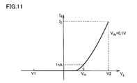
- drain current (I d )is measured by changing gate voltage (V g ).
- V ggate voltage
- the threshold voltage (V th )is a gate voltage at which a drain current starts to flow. More specifically, the threshold voltage (V th ) is a gate voltage when the drain voltage is 0.1 V, the source voltage is 0 V, and the drain current is 1 nA.
- the voltage (V ds ) between the source and drainis 0.1V.
- the drain currentis measured by changing the gate voltage applied to the semiconductor device.
- a gate voltage at which the drain current becomes 1 nAis defined as a first threshold voltage (V th1 ).
- stressis applied to the semiconductor device.
- the drain voltageis measured by changing the gate voltage.
- a gate voltage at which the drain current becomes 1 nAis set as a second threshold voltage (V th2 ).
- V th1first threshold voltage
- V th2second threshold voltage
- the operationis checked for a shipping inspection, and then the semiconductor device is shipped.
- the first threshold voltage of the semiconductor device measured for the first timeincludes a case where the first threshold voltage is measured by applying a voltage to the gate electrode for the first time after the semiconductor device is shipped.
- the semiconductor device according to the present inventionit is possible to provide a semiconductor device in which fluctuations in electrical characteristics such as a threshold voltage are sufficiently suppressed.
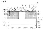
- FIG. 1is a schematic cross-sectional view showing a structure of a MOSFET according to a first embodiment.
- FIG. 2is a schematic cross-sectional view showing an enlarged structure of a MOSFET according to the first embodiment.
- 3is a flowchart schematically showing a method for manufacturing the semiconductor device according to the first embodiment.
- FIG. 6is a schematic cross sectional view for illustrating the method for manufacturing the semiconductor device according to the first embodiment.
- FIG. 6is a schematic cross sectional view for illustrating the method for manufacturing the semiconductor device according to the first embodiment.
- FIG. 6is a schematic cross sectional view for illustrating the method for manufacturing the semiconductor device according to the first embodiment.
- FIG. 6is a schematic cross sectional view for illustrating the method for manufacturing the semiconductor device according to the first embodiment.
- FIG. 6is a schematic cross sectional view for illustrating the method for manufacturing the semiconductor device according to the first embodiment.
- FIG. 6is a schematic cross sectional view for illustrating the method for manufacturing the semiconductor device according to the first embodiment.
- 6is a schematic cross-sectional view showing a structure of a MOSFET according to a second embodiment.
- FIG. 6is a schematic cross-sectional view showing a structure of an SBD according to Embodiment 3.
- FIG.It is a figure which shows the relationship between a gate voltage and a drain current. It is a figure which shows the relationship between a gate voltage and a drain current. It is a figure which shows the relationship between the application time of gate voltage, and the fluctuation
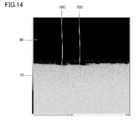
- 3is a HADF-STEM photograph in the MOSFET of the example. It is a mapping figure of the silicon element by EDX in MOSFET of an Example. 3 is a BF-STEM photograph in the MOSFET of the example. 3 is a HADF-STEM photograph in the MOSFET of the example. It is a mapping figure of the silicon element by EDX in MOSFET of the comparative example before voltage application. It is a BF-STEM photograph in the MOSFET of the comparative example before voltage application. It is a HAADDF-STEM photograph in the MOSFET of the comparative example before voltage application. It is a mapping figure of the silicon element by EDX in MOSFET of the comparative example after voltage application. It is a BF-STEM photograph in a MOSFET of a comparative example after voltage application. It is a HAADDF-STEM photograph in the MOSFET of the comparative example after voltage application.
- MOSFET 1is a planar MOSFET, and includes a silicon carbide substrate 10, a gate oxide film 20, a gate electrode 30, a source electrode 40 and a drain electrode 50 as ohmic electrodes, and interlayer insulation.
- the film 60 and the source wiring 41are mainly provided.
- Silicon carbide substrate 10is made of, for example, polytype 4H hexagonal silicon carbide, and includes main surface 10A having an off angle with respect to the ⁇ 0001 ⁇ plane.
- Main surface 10Amay be, for example, a surface having an off angle of 0.1 ° to 8 ° with respect to the ⁇ 0001 ⁇ plane, or a surface having an off angle of 1 ° to 8 °.
- the main surface 10Amay be a surface having an off angle of 62 ° ⁇ 10 ° macroscopically with respect to the ⁇ 0001 ⁇ plane, and may specifically be a (03-38) plane.
- Silicon carbide substrate 10includes a base substrate 11 made of silicon carbide and having an n-type conductivity, a buffer layer 12 made of silicon carbide and having an n-type conductivity, and a drift layer made of silicon carbide and having an n-type conductivity. 13, a pair of body regions 14 having a p-type conductivity, a source region 15 having an n-type conductivity, and a contact region 16 having a p-type conductivity.
- Silicon carbide substrate 10may be any substrate that includes silicon carbide in part, and base substrate 11 is not limited to a substrate made of silicon carbide.
- the base substrate 11may be made of, for example, silicon (Si), gallium nitride (GaN), aluminum nitride (AlN), a mixed crystal of gallium nitride and aluminum nitride (AlGaN), or the like.
- the buffer layer 12is formed on one main surface 11A of the base substrate 11 and has an n-type conductivity by including an n-type impurity.
- Drift layer 13is formed on buffer layer 12 and has an n-type conductivity by including an n-type impurity.
- the n-type impurity contained in the drift layer 13is nitrogen (N), for example, and is contained at a lower concentration (density) than the n-type impurity contained in the buffer layer 12.
- Buffer layer 12 and drift layer 13are epitaxially grown layers formed on one main surface 11 ⁇ / b> A of base substrate 11.
- the pair of body regions 14are formed separately from each other in the epitaxial growth layer, and have a p-type conductivity by including p-type impurities (impurities whose conductivity type is p-type).
- the p-type impurity contained in body region 14is, for example, aluminum (Al), boron (B), or the like.
- the source region 15includes the main surface 10 ⁇ / b> A and is formed inside each of the pair of body regions 14 so as to be surrounded by the body region 14.
- Source region 15contains n-type impurities (impurities whose conductivity type is n-type), such as phosphorus (P), at a higher concentration (density) than n-type impurities contained in drift layer 13.
- the contact region 16includes the main surface 10 ⁇ / b> A, is surrounded by the body region 14, and is formed inside each of the pair of body regions 14 so as to be adjacent to the source region 15.
- Contact region 16contains a p-type impurity, such as Al, at a higher concentration (density) than the p-type impurity contained in body region 14.
- Gate oxide film 20is formed in contact with main surface 10 ⁇ / b> A of silicon carbide substrate 10.
- Gate oxide film 20is made of, for example, silicon dioxide, and is formed on main surface 10 ⁇ / b> A so as to extend from one source region 15 to the other source region 15.
- the gate electrode 30is formed on the gate oxide film 20 so as to extend from one source region 15 to the other source region 15. Gate electrode 30 is formed in contact with gate oxide film 20 so as to sandwich gate oxide film 20 with silicon carbide substrate 10.
- the gate electrode 30is made of a conductor such as polysilicon or Al to which impurities are added.
- the source electrode 40is formed in contact with the main surface 10A (on the source region 15 and the contact region 16) of the silicon carbide substrate 10.
- the source electrode 40is made of, for example, a TiAlSi (titanium aluminum silicide) alloy or a NiSi (nickel silicide) alloy, and includes at least one metal of Ni, Ti, and Al, and silicon (Si). Thereby, good ohmic contact is ensured between silicon carbide substrate 10 and source electrode 40.
- the structure of the contact interface between silicon carbide substrate 10 and source electrode 40will be described in detail later.
- Drain electrode 50is formed in contact with main surface 10B opposite to main surface 10A in silicon carbide substrate 10.
- Drain electrode 50is made of TiAlSi alloy, NiSi alloy or the like, like source electrode 40, and is in ohmic contact with silicon carbide substrate 10.
- the source electrode 40 and the drain electrode 50are configured such that a current (I ds ) flowing between the source electrode 40 and the drain electrode 50 can be controlled by a gate voltage (V g ) applied to the gate electrode 30.
- Interlayer insulating film 60is made of, for example, silicon dioxide (SiO 2 ) or silicon nitride (SiN), and is formed so as to surround gate electrode 30 together with gate oxide film 20.
- the film thickness of the interlayer insulating film 60is, for example, not less than 0.5 ⁇ m and not more than 2.0 ⁇ m.
- a region where base surface 10 ⁇ / b> C is exposedis formed on main surface 10 ⁇ / b> A of silicon carbide substrate 10, and is in contact with source electrode 40 in the region. That is, the basal plane 10 ⁇ / b> C is exposed at least at a part of the contact interface with the source electrode 40 in the silicon carbide substrate 10.
- a plurality of base surfaces 10Care exposed at the contact interface, and are in contact with the source electrode 40 at the base surfaces 10C.
- the basal plane 10Cis the (0001) plane.
- the silicon surface and the main surface 10Ais a surface having an off angle of 0.1 ° to 8 ° (1 ° to 8 °) with respect to the (000-1) surface
- 10Cis a (000-1) (carbon surface)
- the base surface 10Cis a (01-12) surface.
- length L in the off-angle direction of basal plane 10Cmay be, for example, not less than 36 nm and not more than 430 nm.
- the length L of the basal plane 10Cis less than 36 nm, it is difficult to sufficiently secure a region where the basal plane 10C is exposed at the contact interface with the source electrode 40 of the silicon carbide substrate 10.
- the length L of the basal plane 10Cexceeds 430 nm, there is a possibility that the electrode material spikes n-type SiC (source region 15).
- the length L of the basal planeis preferably 36 nm or more and 430 nm or less, so that fluctuations in the threshold voltage of the MOSFET 1 can be further suppressed.
- the length L of the base surface 10C in the off-angle directionis the length of the base surface 10C in the off direction of the base surface 10C with respect to the main surface 10A.
- the length L of the basal plane 10Cis not less than 36 nm and not more than 430 nm, the height H is not less than 5 nm and not more than 15 nm.
- the length L of the basal plane 10Cis preferably 36 nm or more and 430 nm or less, and more preferably 50 nm or more and 143 nm or less.
- the state in which the basal plane 10C is exposed as shown in FIG. 2is, for example, EDX (Energy Dispersive X-ray spectroscopy), BF (Bright Light Field) -STEM (Scanning Transmission ElectronHD This can be confirmed by observing the cross-sectional structure of the MOSFET 1 using a Dark-field) -STEM.
- the structure as shown in FIG. 2is formed not only at the contact interface between source electrode 40 and silicon carbide substrate 10 but also at the contact interface between drain electrode 50 and silicon carbide substrate 10. May be.
- MOSFET 1the operation of MOSFET 1 will be described.
- the voltage of gate electrode 30is lower than the threshold voltage, that is, in the off state, body region 14 and drift layer positioned immediately below gate oxide film 20 even when a voltage is applied to drain electrode 50
- the pn junction with 13is reverse-biased and becomes non-conductive.
- a voltage equal to or higher than the threshold voltageis applied to the gate electrode 30
- an inversion layeris formed in the channel region in the vicinity of the body region 14 in contact with the gate oxide film 20.
- the source region 15 and the drift layer 13are electrically connected, and a current flows between the source electrode 40 and the drain electrode 50.
- variation of the threshold voltage of MOSFET1is suppressed as follows. That is, the first threshold voltage (V th1 ) of the MOSFET 1 measured for the first time with respect to the MOSFET 1 and the second threshold voltage (V th2 ) of the MOSFET 1 measured after applying stress to the MOSFET 1 continuously for 1000 hours. Is within ⁇ 0.2V.
- stress applicationmeans that a gate voltage of ⁇ 15 V is applied to the gate electrode 30 in a state where the source voltage of the source electrode 40 is 0 V and the drain voltage of the drain electrode 50 is 0 V.
- the difference between the first threshold voltage (V th1 ) and the third threshold voltage (V th3 ) measured after an arbitrary period of time up to 1000 hours after starting stress application to the MOSFET 1is ⁇ More preferably, it is within 0.2V.
- the stress application to MOSFET 1may be performed, for example, at room temperature or at a temperature of 150 ° C.
- the difference between the first threshold voltage (V th1 ) and the second threshold voltage (V th2 )is within ⁇ 0.2 V regardless of whether the stress is applied at room temperature or 150 ° C.
- MOSFET 1according to the present embodiment is manufactured.
- a silicon carbide substrate preparation stepis performed as a step (S10).
- a base substrate preparation step (S11), an epitaxial growth step (S12), and an ion implantation step (S13)are sequentially performed.
- step (S11)base substrate 11 made of single crystal silicon carbide is prepared by cutting an ingot (not shown) made of 4H—SiC or the like.
- step (S12)buffer layer 12 and drift layer 13 made of silicon carbide are sequentially formed on one main surface 11A of base substrate 11 by epitaxial growth.
- ion implantation for forming body region 14is performed. Specifically, for example, Al (aluminum) ions are implanted into drift layer 13 to form body region 14.
- ion implantation for forming the source region 15is performed. Specifically, for example, P (phosphorus) ions are implanted into the body region 14 to form the source region 15 in the body region 14.
- ion implantation for forming the contact region 16is performed. Specifically, for example, Al ions are implanted into the body region 14 to form the contact region 16 in the body region 14.
- the ion implantationcan be performed on the drift layer 13 by forming a mask layer made of, for example, silicon dioxide and having an opening in a desired region where ion implantation is to be performed.
- base substrate 11made of silicon carbide of n type conductivity
- buffer layer 12made of silicon carbide and n type conductivity
- drift layer 13made of silicon carbide and n type conductivity
- Silicon carbide substrate 10including a body region 14 having a p-type conductivity, a source region 15 having an n-type conductivity, and a contact region 16 having a p-type conductivity is prepared.
- Main surface 10A of silicon carbide substrate 10may be a surface having an off angle of 0.1 ° to 8 ° with respect to the ⁇ 0001 ⁇ plane, for example, and may have an off angle of 1 ° to 8 °. It may be a surface having.
- an activation annealing stepis performed as a step (S20).
- silicon carbide substrate 10is heated in an inert gas atmosphere such as argon. Thereby, the impurities implanted in the step (S13) are activated.
- a gate oxide film forming stepis performed.
- silicon carbide substrate 10is heated at a temperature of 1100 ° C. or higher and 1400 ° C. or lower in an atmosphere gas containing oxygen (dry oxidation).
- gate oxide film 20 made of silicon dioxideis formed to be in contact with main surface 10 ⁇ / b> A of silicon carbide substrate 10.
- a nitrogen annealing stepis performed as a step (S40).
- silicon carbide substrate 10is heated at a temperature of 1100 ° C. or higher and 1400 ° C. or lower in an atmospheric gas such as nitrogen monoxide (NO).
- an atmospheric gassuch as nitrogen monoxide (NO)
- nitrogen atomsare trapped in traps (not shown) existing in the interface region between gate oxide film 20 and silicon carbide substrate 10, and as a result, formation of interface states in the interface region is suppressed.
- silicon carbide substrate 10is further heated at a temperature of 1100 ° C. or higher and 1400 ° C. or lower under an atmospheric gas such as nitrogen (N 2 ) (POA (Post Oxidation Annealing) process).
- N 2nitrogen
- a gate electrode forming stepis performed.
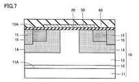
- this step (S50)referring to FIG. 7, for example, an LP (Low Pressure) -CVD (Chemical Vapor Deposition) method is used.
- a gate electrode 30 made of polysilicon having an impurity added to the densityis formed on the gate oxide film 20 so as to be in contact therewith.
- interlayer insulating film forming stepis performed.
- interlayer insulating film 60film thickness: 0.5 ⁇ m or more and 2.0 ⁇ m or less
- gate oxide film 20by, eg, CVD. It is formed so as to surround the gate electrode 30.
- an ohmic electrode forming stepis performed.
- this step (S70)referring to FIG. 8, first, in a region where source electrode 40 is to be formed, interlayer insulating film 60 and gate oxide film 20 are removed, and source region 15 and contact region 16 are exposed. Is formed. In this region, for example, a Ti film, a mixed film of Ti and Al and Si, or a mixed film, or a Ni and Si stacked film or mixed film is formed. Specifically, the metal film is formed in the region by patterning using lift-off or dry etching. On the other hand, the metal film is similarly formed on main surface 10B opposite to main surface 10A in silicon carbide substrate 10.
- silicon carbide substrate 10is held at a temperature of 850 ° C. or higher and 1100 ° C. or lower for 0.5 to 15 minutes in an atmosphere of an inert gas such as nitrogen or argon.
- an inert gassuch as nitrogen or argon.
- a source wiring forming stepis performed.
- source wiring 41 made of Al as a conductoris formed so as to cover interlayer insulating film 60 and source electrode 40, for example, by vapor deposition.
- MOSFET 2as a semiconductor device according to the second embodiment which is another embodiment of the present invention will be described.
- MOSFET 2 according to the present embodimentbasically has the same configuration as MOSFET 1, operates in the same manner, and produces the same effects.
- MOSFET 1is a planar MOSFET
- MOSFET 2 according to the present embodimentis different in structure in that it is a trench MOSFET.
- MOSFET 2is a trench type MOSFET, and similarly to MOSFET 1 according to the first embodiment, silicon carbide substrate 10, gate oxide film 20, gate electrode 30, and ohmic electrode are used. Source electrode 40 and drain electrode 50, interlayer insulating film 60, and source wiring 41 are mainly provided. Silicon carbide substrate 10 has a trench 70 opened to the main surface 10A side. Trench 70 includes a sidewall surface 70A and a bottom surface 70B, penetrating source region 15 and body region 14 such that sidewall surface 70A extends to source region 15, body region 14 and drift layer 13, and bottom surface 70B is drift layer 13. It is formed so that it may be located in. Main surface 10A has an off angle of, for example, 0.1 ° to 8 °, preferably 1 ° to 8 ° with respect to the ⁇ 0001 ⁇ plane.
- the body region 14is formed on the side opposite to the base substrate 11 side when viewed from the drift layer 13.
- Body region 14includes sidewall surface 70A, and is formed to extend in contact with drift layer 13 in a direction away from sidewall surface 70A.
- Body region 14has a p-type conductivity by containing a p-type impurity.
- the p-type impurity contained in body region 14is, for example, Al (aluminum), B (boron), or the like.
- the source region 15is formed on the side opposite to the drift layer 13 when viewed from the body region 14.
- Source region 15includes sidewall surface 70A, and is formed to extend in contact with body region 14 in a direction away from sidewall surface 70A.
- Source region 15has an n-type conductivity by containing an n-type impurity.
- the concentration value of the n-type impurity contained in the source region 15is higher than the concentration value of the n-type impurity contained in the drift layer 13.
- the n-type impurity contained in the source region 15is, for example, P (phosphorus).
- the contact region 16is formed so as to be adjacent to the source region 15 while being in contact with the body region 14.
- Contact region 16has a p-type conductivity by containing a p-type impurity.
- the concentration value of the p-type impurity contained in the contact region 16is higher than the concentration value of the p-type impurity contained in the body region 14.
- the p-type impurity contained in the contact region 16is, for example, Al, B, etc., like the p-type impurity contained in the body region 14.
- Gate oxide film 20is formed in contact with silicon carbide substrate 10, and specifically, is formed to cover side wall surface 70 ⁇ / b> A and bottom surface 70 ⁇ / b> B of trench 70 and main surface 10 ⁇ / b> A of silicon carbide substrate 10. .
- Gate oxide film 20is made of, for example, silicon dioxide.
- Gate electrode 30is formed in contact with gate oxide film 20 so as to sandwich gate oxide film 20 between silicon carbide substrate 10, and specifically, is formed to fill trench 70. .
- the gate electrode 30is made of a conductor such as polysilicon or Al to which impurities are added, for example.
- the source electrode 40is formed in contact with the main surface 10A (on the source region 15 and the contact region 16) of the silicon carbide substrate 10.
- the source electrode 40is made of a TiAlSi alloy or a NiSi alloy as in the first embodiment.
- the interlayer insulating film 60is formed so as to surround the gate electrode 30 together with the gate oxide film 20, and electrically insulates the gate electrode 30 from the source electrode 40 and the source wiring 41.
- Interlayer insulating film 60is made of, for example, silicon dioxide or silicon nitride.
- the source wiring 41is formed so as to cover the interlayer insulating film 60 and the source electrode 40.
- Source wiring 41is made of a conductor such as Al, and is electrically connected to source region 15 via source electrode 40.
- Drain electrode 50is formed in contact with the main surface 10B opposite to the main surface 10A side in the silicon carbide substrate 10.
- Drain electrode 50is made of a material that can make ohmic contact with silicon carbide substrate 10, for example, the same material as source electrode 40, and is electrically connected to silicon carbide substrate 10.
- the contact interface between the source electrode 40 and the silicon carbide substrate 10 and the contact interface between the drain electrode 50 and the silicon carbide substrate 10are configured in the same manner as in the first embodiment (see FIG. 2). Thereby, the MOSFET 2 has the threshold voltage variation suppressed as in the MOSFET 1 according to the first embodiment.
- SBD 3mainly includes silicon carbide substrate 80, Schottky electrode 91, ohmic electrode 92, wiring 93, and pad electrode 94.
- Silicon carbide substrate 80includes a base substrate 81, a buffer layer 82, and a semiconductor layer 83.
- Base substrate 81is made of silicon carbide, and has an n-type conductivity by containing an n-type impurity such as nitrogen.
- Buffer layer 82is formed by epitaxial growth on the main surface of base substrate 81. As with the base substrate 81, the buffer layer 82 has n-type conductivity.
- the semiconductor layer 83is formed on the main surface of the buffer layer 82 opposite to the base substrate 81 side.
- the semiconductor layer 83has an n-type conductivity similar to the base substrate 81 and the buffer layer 82.
- Schottky electrode 91is formed in contact with the main surface of silicon carbide substrate 80.
- a metal constituting Schottky electrode 91as a metal capable of making a Schottky contact with silicon carbide substrate 80, for example, titanium (Ti), tungsten (W), molybdenum (Mo), nickel (Ni), At least one metal selected from the group consisting of tantalum (Ta) and gold (Au) can be employed.
- the wiring 93is made of a conductor such as Al and is formed on the Schottky electrode 91.
- the ohmic electrode 92is formed in contact with the main surface of the silicon carbide substrate 80 opposite to the Schottky electrode 91 side.
- the ohmic electrode 92is made of a TiAlSi alloy, a NiSi alloy, or the like as in the first and second embodiments, and is in ohmic contact with the silicon carbide substrate 80.
- the pad electrode 94is made of a conductor such as Al and is formed on the ohmic electrode 92.
- the contact interface between ohmic electrode 92 and silicon carbide substrate 80is configured in the same manner as in the first and second embodiments (see FIG. 2). Thereby, as in the case of the first and second embodiments, SBD 3 is configured such that fluctuations in electrical characteristics due to the contact state between ohmic electrode 92 and silicon carbide substrate 80 are suppressed.
- the semiconductor device of the present inventionmay be, for example, a JFET (Junction Field Effect Transistor), an IGBT (Insulated Gate Bipolar Transistor), or a PIN (P-Intrinsic-N) diode, and an ohmic electrode of these semiconductor devices.
- a structure as shown in FIG. 2may be formed at the contact interface with the silicon carbide substrate.
- MOSFET 1 according to the first embodimentwas prepared (see Example, FIG. 1).
- the threshold voltage (V th1 ) of the MOSFET 1 before the voltage was appliedwas measured.
- a voltage of ⁇ 15 Vis applied to the gate electrode 30 for a predetermined time, and the threshold voltage (V th2 ) is measured again every application time.
- the threshold voltage (V th )is as described with reference to FIGS. 11 and 12.
- a MOSFET (MOSFET having no structure shown in FIG. 2) in which the basal plane 10C is not exposed at the contact interface with the source electrode 40 in the silicon carbide substrate 10is prepared, and an experiment similar to the above is performed. Went. Further, the MOSFETs of the above examples and comparative examples were cut in the thickness direction, and the structure of the contact interface between the source electrode 40 and the silicon carbide substrate 10 was analyzed by EDX, BF-STEM, and HAADDF-STEM.
- FIG. 13shows the result of calculating the fluctuation value ( ⁇ V th ) of the threshold voltage for each application time of the gate voltage.
- the horizontal axisrepresents the gate voltage application time (h), and the vertical axis represents the threshold voltage fluctuation value ( ⁇ V th (V)).
- the value (absolute value) of ⁇ V thwas greatly reduced as compared with the case of the comparative example. From this result, it was found that the fluctuation of the threshold voltage can be sufficiently suppressed according to the semiconductor device of the present invention.
- FIGS. 14 to 19are Si mapping diagrams by EDX (see FIGS. 14 and 17) and BF-STEM photographs (see FIGS. 15 and 18) at the contact interface between the source electrode 40 and the silicon carbide substrate 10 in the embodiment. ) And HAADDF-STEM photographs (see FIGS. 16 and 19), respectively.
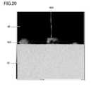
- 20 to 22are Si mapping diagrams by EDX (see FIG. 20), BF-STEM photograph (see FIG. 21), and HAADDF-STEM photograph (see FIG. 22) at the contact interface in the comparative example before voltage application. Each).
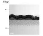
- FIGS. 23 to 25are diagrams of Si mapping by EDX (see FIG. 23), BF-STEM photograph (see FIG.
- the semiconductor device of the present inventioncan be particularly advantageously applied to a semiconductor device that is required to suppress fluctuations in electrical characteristics.
Landscapes
- Engineering & Computer Science (AREA)
- Physics & Mathematics (AREA)
- Condensed Matter Physics & Semiconductors (AREA)
- General Physics & Mathematics (AREA)
- Manufacturing & Machinery (AREA)
- Computer Hardware Design (AREA)
- Microelectronics & Electronic Packaging (AREA)
- Power Engineering (AREA)
- Chemical & Material Sciences (AREA)
- Crystallography & Structural Chemistry (AREA)
- Electrodes Of Semiconductors (AREA)
Abstract
Description
Translated fromJapanese本発明は、半導体装置に関するものであり、より特定的には、電気特性の変動が抑制された半導体装置に関するものである。The present invention relates to a semiconductor device, and more particularly to a semiconductor device in which fluctuations in electrical characteristics are suppressed.
近年、半導体装置の高耐圧化、低損失化などを可能とするため、半導体装置を構成する材料として炭化珪素の採用が進められている。炭化珪素は、従来より半導体装置を構成する材料として広く用いられている珪素に比べてバンドギャップが大きいワイドバンドギャップ半導体である。そのため、半導体装置を構成する材料として炭化珪素を採用することにより、半導体装置の高耐圧化、オン抵抗の低減などを達成することができる。また、炭化珪素を材料として採用した半導体装置は、珪素を材料として採用した半導体装置に比べて、高温環境下で使用された場合の特性の低下が小さいという利点も有している。In recent years, silicon carbide has been adopted as a material constituting a semiconductor device in order to enable a semiconductor device to have a high breakdown voltage and low loss. Silicon carbide is a wide band gap semiconductor having a larger band gap than silicon that has been widely used as a material constituting a semiconductor device. Therefore, by adopting silicon carbide as a material constituting the semiconductor device, it is possible to achieve a high breakdown voltage and a low on-resistance of the semiconductor device. In addition, a semiconductor device that employs silicon carbide as a material has an advantage that a decrease in characteristics when used in a high temperature environment is small as compared with a semiconductor device that employs silicon as a material.
炭化珪素を構成材料とする半導体装置としては、たとえばMOSFET(Metal Oxide Semiconductor Field Effect Transistor)やSBD(Schottky Brrier Diode)などがある。MOSFETは、所定の閾値電圧を境としてチャネル領域における反転層の形成の有無を制御し、電流の導通および遮断をする半導体装置である。このMOSFETにおいては、電流の導通および遮断の境となる閾値電圧が変動することにより、安定な動作が得られないという問題がある。これに対して、たとえばゲート酸化膜の形成条件の検討により閾値電圧の不安定性を低減することなどが提案されている(たとえば、岡本 光央ら、「4H-SiC カーボン面 MOSFETにおけるVth不安定性の低減」、第59回応用物理学関係連合講演会 講演予稿集、応用物理学会、2012年3月、pp15-309(非特許文献1)参照)。As a semiconductor device using silicon carbide as a constituent material, for example, there are a MOSFET (Metal Oxide Semiconductor Field Effect Transistor) and an SBD (Schottky Brier Diode). A MOSFET is a semiconductor device that controls whether or not an inversion layer is formed in a channel region with a predetermined threshold voltage as a boundary, thereby conducting and interrupting current. In this MOSFET, there is a problem that a stable operation cannot be obtained because the threshold voltage that is a boundary between current conduction and interruption varies. In contrast, for example, it has been proposed to reduce the instability of the threshold voltage by examining the formation conditions of the gate oxide film (for example, Mitsuo Okamoto et al., “Vth instability of 4H-SiC carbon surface MOSFET "Reduction", 59th Joint Conference on Applied Physics, Preliminary Proceedings, Japan Society of Applied Physics, March 2012, pp15-309 (Non-patent Document 1)).
上述のように、MOSFETにおける閾値電圧の変動を抑制するための提案はなされているものの、その詳細な原因などについての知見は得られていなかった。そのため、従来のMOSFETでは、閾値電圧などの電気特性の変動を十分に抑制することが困難であった。そこで、本発明の目的は、閾値電圧などの電気特性の変動が十分に抑制された半導体装置を提供することである。As described above, although proposals have been made to suppress fluctuations in threshold voltage in MOSFETs, no knowledge has been obtained about the detailed cause thereof. Therefore, it has been difficult for conventional MOSFETs to sufficiently suppress fluctuations in electrical characteristics such as threshold voltage. Accordingly, an object of the present invention is to provide a semiconductor device in which fluctuations in electrical characteristics such as a threshold voltage are sufficiently suppressed.
本発明に従った半導体装置は、{0001}面に対してオフ角を有する主表面を含む炭化珪素基板と、上記主表面に接触して形成されたオーミック電極とを備えている。炭化珪素基板において、オーミック電極との接触界面の少なくとも一部には、基底面が露出している。A semiconductor device according to the present invention includes a silicon carbide substrate including a main surface having an off angle with respect to the {0001} plane, and an ohmic electrode formed in contact with the main surface. In the silicon carbide substrate, the basal plane is exposed at least at a part of the contact interface with the ohmic electrode.
本発明者は、炭化珪素基板上にオーミック電極が形成された構成を有する半導体装置(たとえば、MOSFETなど)において、閾値電圧などの電気特性に変動が生じる原因について詳細な検討を行った結果、以下の知見を得て、本発明に想到した。The present inventor conducted a detailed study on the cause of fluctuations in electrical characteristics such as threshold voltage in a semiconductor device (for example, MOSFET) having a configuration in which an ohmic electrode is formed on a silicon carbide substrate. As a result, the present invention has been conceived.
まず、炭化珪素基板上にオーミック電極が形成された半導体装置では、当該半導体装置に対して電圧が印加される前には、オーミック電極と炭化珪素基板との接触界面付近に電極材料に由来した塊状物が存在している。そして、所定時間だけ電圧が印加された後には、当該塊状物が消失する。つまり、オーミック電極に対する電圧の印加前後において、オーミック電極と炭化珪素基板との接触界面における元素(たとえばオーミック電極がTiAlSi合金である場合にはシリコン元素)の分布状態が変化する。First, in a semiconductor device in which an ohmic electrode is formed on a silicon carbide substrate, before the voltage is applied to the semiconductor device, a lump derived from an electrode material in the vicinity of the contact interface between the ohmic electrode and the silicon carbide substrate. Things exist. Then, after the voltage is applied for a predetermined time, the lump disappears. That is, the distribution state of the element (for example, silicon element when the ohmic electrode is a TiAlSi alloy) at the contact interface between the ohmic electrode and the silicon carbide substrate changes before and after the voltage is applied to the ohmic electrode.
本発明者は、上述のような元素の分布状態の変化が半導体装置の電気特性の変動の原因となっていることに着目し、オーミック電極と炭化珪素基板との接触界面におけるより安定な構造を見出し、本発明に想到した。すなわち、本発明に従った半導体装置では、炭化珪素基板においてオーミック電極との接触界面の少なくとも一部には基底面が露出している。これにより、当該接触界面に基底面が露出しない場合に比べてより安定な構造が得られ、その結果電気特性の変動が緩和される。したがって、本発明に従った半導体装置によれば、電気特性の変動が十分に抑制された半導体装置を提供することができる。The inventor of the present invention pays attention to the fact that the change in the distribution state of the element as described above causes the fluctuation of the electrical characteristics of the semiconductor device, and a more stable structure at the contact interface between the ohmic electrode and the silicon carbide substrate. The headline and the present invention were conceived. That is, in the semiconductor device according to the present invention, the basal plane is exposed at least at a part of the contact interface with the ohmic electrode in the silicon carbide substrate. As a result, a more stable structure can be obtained as compared with the case where the basal plane is not exposed at the contact interface, and as a result, fluctuations in electrical characteristics are alleviated. Therefore, according to the semiconductor device according to the present invention, it is possible to provide a semiconductor device in which fluctuations in electrical characteristics are sufficiently suppressed.
上記半導体装置において、オーミック電極は、Ni、TiおよびAlのうち少なくとも一種の金属を含んでいてもよい。より具体的には、オーミック電極は、TiAlSi合金またはNiSi合金からなっていてもよい。これにより、オーミック電極と炭化珪素基板との間における良好なオーミック接触を確保することができる。In the semiconductor device, the ohmic electrode may contain at least one metal selected from Ni, Ti and Al. More specifically, the ohmic electrode may be made of a TiAlSi alloy or a NiSi alloy. Thereby, good ohmic contact between the ohmic electrode and the silicon carbide substrate can be ensured.
上記半導体装置において、基底面のオフ角方向での長さは、36nm以上430nm以下であってもよい。基底面の上記長さが36nm未満である場合には、炭化珪素基板のオーミック電極との接触界面において、基底面が露出した領域を十分に確保することが困難である。一方、基底面の上記長さが430nmを超える場合には、電極材料がソースのn型SiC領域をスパイク(貫通)し、MOSFET動作に支障をきたすという問題が発生する可能性がある。このような理由から、基底面の上記長さは、36nm以上430nm以下であることが好ましく、さらに50nm以上143nm以下であることがより好ましい。これにより、上記半導体装置の電気特性の変動を一層抑制することができる。In the semiconductor device, the length of the basal plane in the off-angle direction may be not less than 36 nm and not more than 430 nm. When the length of the basal plane is less than 36 nm, it is difficult to sufficiently secure a region where the basal plane is exposed at the contact interface with the ohmic electrode of the silicon carbide substrate. On the other hand, when the length of the basal plane exceeds 430 nm, there is a possibility that the electrode material spikes (penetrates) the source n-type SiC region, thereby hindering MOSFET operation. For these reasons, the length of the basal plane is preferably 36 nm or more and 430 nm or less, and more preferably 50 nm or more and 143 nm or less. Thereby, the fluctuation | variation of the electrical property of the said semiconductor device can be suppressed further.
上記半導体装置は、炭化珪素基板に接触して形成された酸化膜と、炭化珪素基板との間に酸化膜を挟むように酸化膜に接触して形成されたゲート電極と、炭化珪素基板に接触して形成されたドレイン電極とをさらに備えていてもよい。また、オーミック電極は、ソース電極であってもよい。また、ソース電極およびドレイン電極は、ゲート電極に印加されるゲート電圧によってソース電極およびドレイン電極の間に流れる電流が制御可能に構成されていてもよい。また、初めて測定される半導体装置の第1の閾値電圧と、1000時間継続的に半導体装置に対してストレス印加した後に測定される半導体装置の第2の閾値電圧との差が±0.2V以内であってもよい。ここで、ストレス印加とは、ソース電極の電圧が0Vでありかつドレイン電極の電圧が0Vの状態で、ゲート電極に対して-15Vのゲート電圧を印加することである。これにより、閾値電圧の変動が一層抑制された半導体装置を提供することができる。The semiconductor device is in contact with an oxide film formed in contact with a silicon carbide substrate, a gate electrode formed in contact with the oxide film so as to sandwich the oxide film between the silicon carbide substrate, and the silicon carbide substrate. And a drain electrode formed as described above. The ohmic electrode may be a source electrode. The source electrode and the drain electrode may be configured such that a current flowing between the source electrode and the drain electrode can be controlled by a gate voltage applied to the gate electrode. Further, the difference between the first threshold voltage of the semiconductor device measured for the first time and the second threshold voltage of the semiconductor device measured after applying stress to the semiconductor device continuously for 1000 hours is within ± 0.2V. It may be. Here, stress application means that a gate voltage of −15 V is applied to the gate electrode while the voltage of the source electrode is 0 V and the voltage of the drain electrode is 0 V. Thereby, it is possible to provide a semiconductor device in which the fluctuation of the threshold voltage is further suppressed.
ここで、閾値電圧の定義について図11および図12を参照して説明する。図11および図12において、横軸はゲート電圧(Vg)、縦軸はドレイン電流(Id)を示している。図11を参照して、まず、ゲート電圧(Vg)を変化させてドレイン電流(Id)を測定する。ゲート電圧がマイナスの場合はドレイン電流はほとんど流れないが、ゲート電圧を大きくしていくとドレイン電流が急に流れ始める。閾値電圧(Vth)は、ドレイン電流が流れ始めるゲート電圧のことである。より詳細には、閾値電圧(Vth)は、ドレイン電圧が0.1Vであり、ソース電圧が0Vであって、ドレイン電流が1nAであるときのゲート電圧のことである。なお、ソースドレイン間の電圧(Vds)は0.1Vである。Here, the definition of the threshold voltage will be described with reference to FIGS. 11 and 12, the horizontal axis indicates the gate voltage (Vg ), and the vertical axis indicates the drain current (Id ). Referring to FIG. 11, first, drain current (Id ) is measured by changing gate voltage (Vg ). When the gate voltage is negative, almost no drain current flows, but when the gate voltage is increased, the drain current starts to flow suddenly. The threshold voltage (Vth ) is a gate voltage at which a drain current starts to flow. More specifically, the threshold voltage (Vth ) is a gate voltage when the drain voltage is 0.1 V, the source voltage is 0 V, and the drain current is 1 nA. The voltage (Vds ) between the source and drain is 0.1V.
次に、閾値電圧の変動について図12を参照して説明する。まず、半導体装置に印加されるゲート電圧を変化させてドレイン電流を測定する。ドレイン電流が1nAになるゲート電圧を第1の閾値電圧(Vth1)とする。次に、半導体装置に対してストレスを印加する。その後、ゲート電圧を変化させてドレイン電流を測定する。そして、ドレイン電流が1nAになるゲート電圧を第2の閾値電圧(Vth2)とする。このように、閾値電圧はストレス印加により変動する。Next, threshold voltage fluctuation will be described with reference to FIG. First, the drain current is measured by changing the gate voltage applied to the semiconductor device. A gate voltage at which the drain current becomes 1 nA isdefined as a first threshold voltage (Vth1 ). Next, stress is applied to the semiconductor device. Thereafter, the drain voltage is measured by changing the gate voltage. A gate voltage at which the drain current becomes 1 nA is set as a second threshold voltage (Vth2 ). As described above, the threshold voltage varies with the application of stress.
通常、半導体装置の製造が完了した後、出荷検査などのため動作確認を行い、その後半導体装置が出荷される。本発明において、初めて測定される半導体装置の第1の閾値電圧とは、半導体装置が出荷された後に初めてゲート電極に電圧を印加して第1の閾値電圧を測定する場合を含む。Usually, after the manufacturing of the semiconductor device is completed, the operation is checked for a shipping inspection, and then the semiconductor device is shipped. In the present invention, the first threshold voltage of the semiconductor device measured for the first time includes a case where the first threshold voltage is measured by applying a voltage to the gate electrode for the first time after the semiconductor device is shipped.
以上の説明から明らかなように、本発明に従った半導体装置によれば、閾値電圧などの電気特性の変動が十分に抑制された半導体装置を提供することができる。As is apparent from the above description, according to the semiconductor device according to the present invention, it is possible to provide a semiconductor device in which fluctuations in electrical characteristics such as a threshold voltage are sufficiently suppressed.
以下、図面に基づいて本発明の実施の形態を説明する。なお、以下の図面において同一または相当する部分には同一の参照番号を付し、その説明は繰返さない。また、本明細書中の結晶学的記載においては、個別方位を[]、集合方位を<>、個別面を()、集合面を{}でそれぞれ示している。また、負の指数については、結晶学上、”‐”(バー)を数字の上に付けることになっているが、本明細書中では、数字の前に負の符号を付けている。Hereinafter, embodiments of the present invention will be described with reference to the drawings. In the following drawings, the same or corresponding parts are denoted by the same reference numerals, and description thereof will not be repeated. In the crystallographic description in this specification, the individual orientation is indicated by [], the collective orientation is indicated by <>, the individual plane is indicated by (), and the collective plane is indicated by {}. As for the negative index, “−” (bar) is attached on the number in crystallography, but in this specification, a negative sign is attached before the number.
(実施の形態1)
まず、本発明の一実施の形態である実施の形態1に係る半導体装置としてのMOSFET1の構造について説明する。図1を参照して、MOSFET1は、プレーナ型のMOSFETであって、炭化珪素基板10と、ゲート酸化膜20と、ゲート電極30と、オーミック電極としてのソース電極40およびドレイン電極50と、層間絶縁膜60と、ソース配線41とを主に備えている。(Embodiment 1)
First, the structure of
炭化珪素基板10は、たとえばポリタイプ4Hの六方晶炭化珪素からなっており、{0001}面に対してオフ角を有する主表面10Aを含んでいる。主表面10Aは、たとえば{0001}面に対して0.1°以上8°以下のオフ角を有する面であってもよく、1°以上8°以下のオフ角を有する面であってもよい。また、主表面10Aは、{0001}面に対して巨視的に62°±10°のオフ角を有する面であってもよく、具体的には(03-38)面であってもよい。
炭化珪素基板10は、炭化珪素からなり導電型がn型であるベース基板11と、炭化珪素からなり導電型がn型であるバッファ層12と、炭化珪素からなり導電型がn型のドリフト層13と、導電型がp型の一対のボディ領域14と、導電型がn型のソース領域15と、導電型がp型のコンタクト領域16とを含んでいる。また、炭化珪素基板10は、炭化珪素を一部に含む基板であればよく、ベース基板11は炭化珪素からなるものには限定されない。ベース基板11は、たとえばシリコン(Si)、窒化ガリウム(GaN)、窒化アルミニウム(AlN)、窒化ガリウムと窒化アルミニウムの混晶(AlGaN)などからなっていてもよい。
バッファ層12は、ベース基板11の一方の主表面11A上に形成され、n型不純物を含むことにより導電型がn型となっている。ドリフト層13は、バッファ層12上に形成され、n型不純物を含むことにより導電型がn型となっている。ドリフト層13に含まれるn型不純物は、たとえば窒素(N)であり、バッファ層12に含まれるn型不純物よりも低い濃度(密度)で含まれている。バッファ層12およびドリフト層13は、ベース基板11の一方の主表面11A上に形成されたエピタキシャル成長層である。The
一対のボディ領域14は、エピタキシャル成長層において互いに分離して形成され、p型不純物(導電型がp型である不純物)を含むことにより、導電型がp型となっている。ボディ領域14に含まれるp型不純物は、たとえばアルミニウム(Al)、ホウ素(B)などである。The pair of
ソース領域15は、主表面10Aを含み、かつボディ領域14に取り囲まれるように、一対のボディ領域14のそれぞれの内部に形成されている。ソース領域15は、n型不純物(導電型がn型である不純物)、たとえばリン(P)などをドリフト層13に含まれるn型不純物よりも高い濃度(密度)で含んでいる。The
コンタクト領域16は、主表面10Aを含み、かつボディ領域14に取り囲まれるとともに、ソース領域15に隣接するように一対のボディ領域14のそれぞれの内部に形成されている。コンタクト領域16は、p型不純物、たとえばAlなどをボディ領域14に含まれるp型不純物よりも高い濃度(密度)で含んでいる。The
ゲート酸化膜20は、炭化珪素基板10の主表面10A上に接触するように形成されている。ゲート酸化膜20は、たとえば二酸化珪素からなり、一方のソース領域15上から他方のソース領域15上にまで延在するように主表面10A上において形成されている。
ゲート電極30は、一方のソース領域15上から他方のソース領域15上にまで延在するようにゲート酸化膜20上に接触して形成されている。ゲート電極30は、炭化珪素基板10との間にゲート酸化膜20を挟むようにゲート酸化膜20に接触して形成されている。ゲート電極30は、不純物が添加されたポリシリコンやAlなどの導電体からなっている。The
ソース電極40は、炭化珪素基板10の主表面10A上(ソース領域15およびコンタクト領域16上)に接触するように形成されている。ソース電極40は、たとえばTiAlSi(チタンアルミニウムシリサイド)合金またはNiSi(ニッケルシリサイド)合金などからなり、Ni、TiおよびAlのうち少なくとも一種の金属と、シリコン(Si)とを含んでいる。これにより、炭化珪素基板10とソース電極40との間において良好なオーミック接触が確保されている。なお、炭化珪素基板10とソース電極40との接触界面の構造は、後に詳述する。The
ドレイン電極50は、炭化珪素基板10において主表面10A側とは反対側の主表面10B上に接触して形成されている。ドレイン電極50は、ソース電極40と同様にTiAlSi合金やNiSi合金などからなっており、炭化珪素基板10に対してオーミック接触している。ソース電極40およびドレイン電極50は、ゲート電極30に印加されるゲート電圧(Vg)により、ソース電極40とドレイン電極50との間に流れる電流(Ids)が制御可能に構成されている。
層間絶縁膜60は、たとえば二酸化珪素(SiO2)や窒化珪素(SiN)などからなっており、ゲート酸化膜20とともにゲート電極30を取り囲むように形成されている。層間絶縁膜60の膜厚は、たとえば0.5μm以上2.0μm以下である。
次に、ソース電極40と炭化珪素基板10との接触界面の構造について説明する。図2を参照して、炭化珪素基板10の主表面10Aには、基底面10Cが露出した領域が形成されており、当該領域においてソース電極40と接触している。つまり、炭化珪素基板10においてソース電極40との接触界面の少なくとも一部には、基底面10Cが露出している。また、当該接触界面には複数の基底面10Cが露出しており、それぞれの基底面10Cにおいてソース電極40と接触している。ここで、主表面10Aが(0001)面に対して0.1°以上8°以下(1°以上8°以下)のオフ角を有する面である場合には、基底面10Cは(0001)面(シリコン面)であり、主表面10Aが(000-1)面に対して0.1°以上8°以下(1°以上8°以下)のオフ角を有する面である場合には、基底面10Cは(000-1)(カーボン面)であり、主表面10Aが(03-38)面である場合には、基底面10Cは(01-12)面である。このような構造を有することにより、本実施の形態に係るMOSFET1は、後述するように閾値電圧の変動が抑制されたものとなっている。Next, the structure of the contact interface between the
また、図2を参照して、基底面10Cのオフ角方向での長さLはたとえば36nm以上430nm以下であってもよい。基底面10Cの長さLが36nm未満である場合には、炭化珪素基板10のソース電極40との接触界面において、基底面10Cが露出した領域を十分に確保することが困難である。一方、基底面10Cの長さLが430nmを超える場合には、電極材料がn型SiC(ソース領域15)をスパイクするという可能性がある。このような理由から、基底面の上記長さLは、36nm以上430nm以下であることが好ましく、これによりMOSFET1の閾値電圧の変動を一層抑制することができる。ここで、「基底面10Cのオフ角方向での長さL」とは、主表面10Aに対する基底面10Cのオフ方向における基底面10Cの長さである。また、基底面10Cの長さLが36nm以上430nm以下である場合には、高さHは5nm以上15nm以下である。また、基底面10Cの上記長さLは、36nm以上430nm以下であることが好ましく、50nm以上143nm以下であることがさらに好ましい。Referring to FIG. 2, length L in the off-angle direction of
また、図2に示すような基底面10Cが露出した状態は、たとえばEDX(Energy Dispersive X-ray spectrometry)や、BF(Bright Field)-STEM(Scannning Transmission Electron Microscopy)、あるいはHADDF(High-angle Annular Dark-field)-STEMなどにより、MOSFET1の断面構造を観察することで確認することができる。また、本実施の形態のMOSFET1では、ソース電極40と炭化珪素基板10との接触界面においてだけでなく、ドレイン電極50と炭化珪素基板10との接触界面においても図2に示すような構造が形成されていてもよい。In addition, the state in which the
次に、MOSFET1の動作について説明する。図1を参照して、ゲート電極30の電圧が閾値電圧未満の状態、すなわちオフ状態では、ドレイン電極50に電圧が印加されても、ゲート酸化膜20の直下に位置するボディ領域14とドリフト層13との間のpn接合が逆バイアスとなり、非導通状態となる。一方、ゲート電極30に閾値電圧以上の電圧を印加すると、ボディ領域14のゲート酸化膜20と接触する付近であるチャネル領域において、反転層が形成される。その結果、ソース領域15とドリフト層13とが電気的に接続され、ソース電極40とドレイン電極50との間に電流が流れる。Next, the operation of
また、MOSFET1の閾値電圧の変動が抑制されていることは以下のようにして確認することができる。すなわち、MOSFET1に対して初めて測定されるMOSFET1の第1の閾値電圧(Vth1)と、1000時間継続的にMOSFET1に対してストレス印加した後に測定されるMOSFET1の第2の閾値電圧(Vth2)との差は±0.2V以内である。ここで、ストレス印加とは、ソース電極40のソース電圧が0Vでありかつドレイン電極50のドレイン電圧が0Vの状態で、ゲート電極30に対して-15Vのゲート電圧を印加することである。Moreover, it can confirm that the fluctuation | variation of the threshold voltage of MOSFET1 is suppressed as follows. That is, the first threshold voltage (Vth1 ) of the
また、第1の閾値電圧(Vth1)と、MOSFET1に対してストレス印加を開始した後、1000時間までの任意の時間経過後に測定される第3の閾値電圧(Vth3)との差が±0.2V以内であることがより好ましい。なお、MOSFET1に対するストレス印加は、たとえば室温で行われてもよいし、150℃の温度下で行われてもよい。好ましくは、ストレス印加が室温および150℃のいずれの温度で行われても第1の閾値電圧(Vth1)と第2の閾値電圧(Vth2)との差が±0.2V以内である。In addition, the difference between the first threshold voltage (Vth1 ) and the third threshold voltage (Vth3 ) measured after an arbitrary period of time up to 1000 hours after starting stress application to the
次に、本実施の形態に係る半導体装置の製造方法について説明する。本実施の形態に係る半導体装置の製造方法では、上記本実施の形態に係るMOSFET1が製造される。図3を参照して、本実施の形態に係る半導体装置の製造方法では、まず、工程(S10)として、炭化珪素基板準備工程が実施される。この工程(S10)では、ベース基板準備工程(S11)と、エピタキシャル成長工程(S12)と、イオン注入工程(S13)とが順に実施される。Next, a method for manufacturing a semiconductor device according to the present embodiment will be described. In the method for manufacturing a semiconductor device according to the present embodiment,
まず、工程(S11)では、図4を参照して、4H-SiCなどからなるインゴット(図示しない)を切断することにより、単結晶炭化珪素からなるベース基板11が準備される。次に、工程(S12)では、エピタキシャル成長によりベース基板11の一方の主表面11A上に炭化珪素からなるバッファ層12およびドリフト層13が順次形成される。First, in step (S11), referring to FIG. 4,
次に、工程(S13)では、図5を参照して、まず、ボディ領域14を形成するためのイオン注入が実施される。具体的には、たとえばAl(アルミニウム)イオンがドリフト層13に注入されることにより、ボディ領域14が形成される。次に、ソース領域15を形成するためのイオン注入が実施される。具体的には、たとえばP(リン)イオンがボディ領域14に注入されることにより、ボディ領域14内にソース領域15が形成される。さらに、コンタクト領域16を形成するためのイオン注入が実施される。具体的には、たとえばAlイオンがボディ領域14に注入されることにより、ボディ領域14内にコンタクト領域16が形成される。上記イオン注入は、ドリフト層13上において、たとえば二酸化珪素からなり、イオン注入を実施すべき所望の領域に開口を有するマスク層を形成して実施することができる。Next, in step (S13), referring to FIG. 5, first, ion implantation for forming
これにより、導電型がn型である炭化珪素からなるベース基板11と、炭化珪素からなり導電型がn型であるバッファ層12と、炭化珪素からなり導電型がn型のドリフト層13と、導電型がp型のボディ領域14と、導電型がn型のソース領域15と、導電型がp型のコンタクト領域16とを含む炭化珪素基板10が準備される。また、炭化珪素基板10の主表面10Aは、たとえば{0001}面に対して0.1°以上8°以下のオフ角を有する面であってもよく、1°以上8°以下のオフ角を有する面であってもよい。Thereby,
次に、工程(S20)として、活性化アニール工程が実施される。この工程(S20)では、たとえばアルゴンなどの不活性ガス雰囲気中において炭化珪素基板10が加熱される。これにより、上記工程(S13)において注入された不純物が活性化される。Next, an activation annealing step is performed as a step (S20). In this step (S20),
次に、工程(S30)として、ゲート酸化膜形成工程が実施される。この工程(S30)では、たとえば酸素を含む雰囲気ガス下において炭化珪素基板10が1100℃以上1400℃以下の温度で加熱される(ドライ酸化)。これにより、図6に示すように、二酸化珪素からなるゲート酸化膜20が炭化珪素基板10の主表面10A上に接触するように形成される。Next, as a step (S30), a gate oxide film forming step is performed. In this step (S30), for example,
次に、工程(S40)として、窒素アニール工程が実施される。この工程(S40)では、たとえば一酸化窒素(NO)などの雰囲気ガス下において、炭化珪素基板10が1100℃以上1400℃以下の温度で加熱される。これにより、ゲート酸化膜20と炭化珪素基板10との界面領域に存在するトラップ(図示しない)に窒素原子が捕獲され、その結果当該界面領域における界面準位の形成が抑制される。その後、窒素(N2)などの雰囲気ガス下において1100℃以上1400℃以下の温度で炭化珪素基板10がさらに加熱される(POA(Post Oxidation Annealing)処理)。Next, a nitrogen annealing step is performed as a step (S40). In this step (S40),
次に、工程(S50)として、ゲート電極形成工程が実施される、この工程(S50)では、図7を参照して、たとえばLP(Low Pressure)-CVD(Chemical Vapor Deposition)法などにより、高密度に不純物が添加されたポリシリコンからなるゲート電極30がゲート酸化膜20上に接触するように形成される。Next, as a step (S50), a gate electrode forming step is performed. In this step (S50), referring to FIG. 7, for example, an LP (Low Pressure) -CVD (Chemical Vapor Deposition) method is used. A
次に、工程(S60)として、層間絶縁膜形成工程が実施される。この工程(S60)では、図7を参照して、たとえばCVD法により、二酸化珪素または窒化珪素からなる層間絶縁膜60(膜厚:0.5μm以上2.0μm以下)が、ゲート酸化膜20とともにゲート電極30を取り囲むように形成される。Next, as a step (S60), an interlayer insulating film forming step is performed. In this step (S60), referring to FIG. 7, interlayer insulating film 60 (film thickness: 0.5 μm or more and 2.0 μm or less) made of silicon dioxide or silicon nitride is formed together with
次に、工程(S70)として、オーミック電極形成工程が実施される。この工程(S70)では、図8を参照して、まず、ソース電極40を形成すべき領域において、層間絶縁膜60およびゲート酸化膜20が除去され、ソース領域15およびコンタクト領域16が露出した領域が形成される。そして、当該領域において、たとえばTi、AlおよびSiの積層膜や混合膜、またはNiおよびSiの積層膜や混合膜である金属膜が形成される。具体的には、上記金属膜は、リフトオフまたはドライエッチングを用いてパターニングされることにより、当該領域内に形成される。一方、炭化珪素基板10において主表面10A側とは反対側の主表面10B上においても同様に上記金属膜が形成される。その後、窒素やアルゴンなどの不活性ガスの雰囲気下において、炭化珪素基板10を850℃以上1100℃以下の温度で0.5分以上15分以下の間保持する。このようにして上記金属膜をアニールすることにより、上記金属膜が合金化するとともに上記金属膜の少なくとも一部がシリサイド化される。その結果、TiAlSi合金またはNiSi合金からなるソース電極40およびドレイン電極50がそれぞれ形成される。Next, as a step (S70), an ohmic electrode forming step is performed. In this step (S70), referring to FIG. 8, first, in a region where source electrode 40 is to be formed,
次に、工程(S80)として、ソース配線形成工程が実施される。この工程(S80)では、図1を参照して、たとえば蒸着法により導電体であるAlからなるソース配線41が、層間絶縁膜60およびソース電極40を覆うように形成される。以上の工程(S10)~(S80)が実施されることにより、上記本実施の形態に係るMOFET1が製造され、本実施の形態に係る半導体装置の製造方法が完了する。Next, as a step (S80), a source wiring forming step is performed. In this step (S80), referring to FIG. 1,
(実施の形態2)
次に、本発明の他の実施の形態である実施の形態2に係る半導体装置としてのMOSFET2について説明する。本実施の形態に係るMOSFET2は、基本的にはMOSFET1と同様の構成を備え、同様に動作し、かつ同様の効果を奏する。しかし、MOSFET1はプレーナ型のMOSFETであったのに対し、本実施の形態に係るMOSFET2はトレンチ型のMOSFETである点でその構造が異なっている。(Embodiment 2)
Next,
図9を参照して、MOSFET2は、トレンチ型のMOSFETであって、上記実施の形態1に係るMOSFET1と同様に炭化珪素基板10と、ゲート酸化膜20と、ゲート電極30と、オーミック電極としてのソース電極40およびドレイン電極50と、層間絶縁膜60と、ソース配線41とを主に備えている。炭化珪素基板10には、主表面10A側に開口するトレンチ70が形成されている。トレンチ70は、側壁面70Aと底面70Bとを含み、側壁面70Aがソース領域15、ボディ領域14およびドリフト層13に亘るようにソース領域15およびボディ領域14を貫通し、底面70Bがドリフト層13に位置するように形成されている。主表面10Aは、{0001}面に対してたとえば0.1°以上8°以下、好ましくは1°以上8°以下のオフ角を有している。Referring to FIG. 9,
ボディ領域14は、ドリフト層13から見てベース基板11側とは反対側に形成されている。ボディ領域14は、側壁面70Aを含み、側壁面70Aから離れる向きにおいてドリフト層13と接触しつつ延在するように形成されている。ボディ領域14は、p型不純物を含むことにより導電型がp型となっている。ボディ領域14に含まれるp型不純物は、たとえばAl(アルミニウム)、B(硼素)などである。The
ソース領域15は、ボディ領域14から見てドリフト層13とは反対側に形成されている。ソース領域15は、側壁面70Aを含み、側壁面70Aから離れる向きにおいてボディ領域14と接触しつつ延在するように形成されている。ソース領域15は、n型不純物を含むことにより導電型がn型となっている。ソース領域15に含まれるn型不純物の濃度値は、ドリフト層13に含まれるn型不純物の濃度値よりも高い値となっている。ソース領域15に含まれるn型の不純物は、たとえばP(リン)などである。The
コンタクト領域16は、ボディ領域14に接触しつつ、ソース領域15に隣接するように形成されている。コンタクト領域16は、p型不純物を含むことにより導電型がp型となっている。コンタクト領域16に含まれるp型不純物の濃度値は、ボディ領域14に含まれるp型不純物の濃度値よりも高い値となっている。コンタクト領域16に含まれるp型不純物は、ボディ領域14に含まれるp型不純物と同様に、たとえばAl、Bなどである。The
ゲート酸化膜20は、炭化珪素基板10に接触して形成されており、具体的にはトレンチ70の側壁面70Aおよび底面70B、ならびに炭化珪素基板10の主表面10Aを覆うように形成されている。ゲート酸化膜20は、たとえば二酸化珪素からなっている。
ゲート電極30は、炭化珪素基板10との間にゲート酸化膜20を挟むようにゲート酸化膜20に接触して形成されており、具体的にはトレンチ70内を充填するように形成されている。ゲート電極30は、たとえば不純物が添加されたポリシリコン、Alなどの導電体からなっている。
ソース電極40は、炭化珪素基板10の主表面10A上(ソース領域15およびコンタクト領域16上)に接触するように形成されている。ソース電極40は、上記実施の形態1と同様にTiAlSi合金やNiSi合金からなっている。The
層間絶縁膜60は、ゲート酸化膜20と共にゲート電極30を取囲むように形成されており、ゲート電極30をソース電極40およびソース配線41に対して電気的に絶縁している。層間絶縁膜60は、たとえば二酸化珪素や窒化珪素からなっている。The
ソース配線41は、層間絶縁膜60およびソース電極40を覆うように形成されている。ソース配線41は、たとえばAlなどの導電体からなっており、ソース電極40を介してソース領域15と電気的に接続されている。The
ドレイン電極50は、炭化珪素基板10において主表面10A側とは反対側の主表面10B上に接触して形成されている。ドレイン電極50は、炭化珪素基板10とオーミック接触することができる材料、たとえばソース電極40と同様の材料からなっており、炭化珪素基板10に対して電気的に接続されている。The
ソース電極40と炭化珪素基板10との接触界面、およびドレイン電極50と炭化珪素基板10との接触界面は、上記実施の形態1の場合と同様に構成されている(図2参照)。これにより、MOSFET2は、上記実施の形態1に係るMOSFET1と同様に閾値電圧の変動が抑制されたものとなっている。The contact interface between the
(実施の形態3)
次に、本発明のさらに他の実施の形態である実施の形態3に係る半導体装置としてのショットキーバリアダイオード(SBD:Schottky Barrier Diode)3の構造について説明する。図10を参照して、SBD3は、炭化珪素基板80と、ショットキ―電極91と、オーミック電極92と、配線93と、パッド電極94とを主に備えている。(Embodiment 3)
Next, the structure of a Schottky barrier diode (SBD) 3 as a semiconductor device according to the third embodiment which is still another embodiment of the present invention will be described. Referring to FIG. 10, SBD 3 mainly includes
炭化珪素基板80は、ベース基板81と、バッファ層82と、半導体層83とを含んでいる。ベース基板81は、炭化珪素からなり、たとえば窒素などのn型不純物を含むことにより導電型がn型となっている。バッファ層82は、ベース基板81の主表面上においてエピタキシャル成長により形成されている。バッファ層82は、ベース基板81と同様に導電型がn型となっている。半導体層83は、バッファ層82のベース基板81側とは反対側の主表面上に形成されている。半導体層83は、ベース基板81およびバッファ層82と同様に導電型がn型となっている。
ショットキー電極91は、炭化珪素基板80の主表面上に接触するように形成されている。ショットキー電極91を構成する金属としては、炭化珪素基板80に対してショットキー接触することが可能な金属として、たとえばチタン(Ti)、タングステン(W)、モリブデン(Mo)、ニッケル(Ni)、タンタル(Ta)および金(Au)からなる群より選択される少なくとも一の金属を採用することができる。配線93は、Alなどの導電体からなり、ショットキー電極91上に形成されている。
オーミック電極92は、炭化珪素基板80においてショットキー電極91側とは反対側の主表面上に接触するように形成されている。オーミック電極92は、上記実施の形態1および2と同様にTiAlSi合金やNiSi合金などからなり、炭化珪素基板80に対してオーミック接触している。パッド電極94は、Alなどの導電体からなり、オーミック電極92上に形成されている。また、オーミック電極92と炭化珪素基板80との接触界面は、上記実施の形態1および2の場合と同様に構成されている(図2参照)。これにより、SBD3は、上記実施の形態1および2の場合と同様に、オーミック電極92と炭化珪素基板80との接触状態に起因した電気特性の変動が抑制されたものとなっている。The
上記実施の形態1~3では、本発明の半導体装置の例としてMOSFETやSBDについて説明したが、本発明の半導体装置はこれに限定されるものではない。すなわち、本発明の半導体装置は、たとえばJFET(Junction Field Effect Transistor)、IGBT(Insulated Gate Bipolar Transistor)またはPIN(P-Intrinsic-N)ダイオードなどであってもよく、これらの半導体装置のオーミック電極と炭化珪素基板との接触界面において、図2に示したような構造が形成されていてもよい。これにより、これらの半導体装置においてもMOSFETやSBDと同様に、オーミック電極と炭化珪素基板との接触状態に起因した電気特性の変動を抑制することができる。In the above first to third embodiments, MOSFETs and SBDs have been described as examples of the semiconductor device of the present invention, but the semiconductor device of the present invention is not limited to this. That is, the semiconductor device of the present invention may be, for example, a JFET (Junction Field Effect Transistor), an IGBT (Insulated Gate Bipolar Transistor), or a PIN (P-Intrinsic-N) diode, and an ohmic electrode of these semiconductor devices. A structure as shown in FIG. 2 may be formed at the contact interface with the silicon carbide substrate. Thereby, also in these semiconductor devices, similarly to MOSFET and SBD, it is possible to suppress fluctuations in electrical characteristics due to the contact state between the ohmic electrode and the silicon carbide substrate.
閾値電圧の変動の抑制について本発明の効果を確認する実験を行った。まず、上記実施の形態1に係るMOSFET1を準備した(実施例、図1参照)。次に、電圧が印加される前のMOSFET1の閾値電圧(Vth1)を測定した。そして、ソース電極40の電圧が0V、ドレイン電極50の電圧が0Vの状態で、ゲート電極30に対して-15Vの電圧を所定時間印加し、印加時間ごとに再度閾値電圧(Vth2)を測定し、その測定結果から閾値電圧の変動値(ΔVth=Vth1-Vth2)を算出した。ここで、閾値電圧(Vth)とは、図11および図12を用いて説明した通りである。また、比較例として、炭化珪素基板10においてソース電極40との接触界面に基底面10Cが露出していないMOSFET(図2に示した構造を有さないMOSFET)を準備し、上記と同様の実験を行った。また、上記実施例および比較例のMOSFETを厚み方向に切断し、ソース電極40と炭化珪素基板10との接触界面の構造をEDX、BF-STEMおよびHADDF-STEMにより解析した。An experiment for confirming the effect of the present invention was performed on the suppression of the fluctuation of the threshold voltage. First,
図13は、ゲート電圧の印加時間ごとに閾値電圧の変動値(ΔVth)を算出した結果を示している。図13において、横軸はゲート電圧の印加時間(h)を示し、縦軸は閾値電圧の変動値(ΔVth(V))を示している。図13から明らかなように、実施例の場合では比較例の場合と比べてΔVthの値(絶対値)が大きく低下した。この結果より、本発明の半導体装置によれば、閾値電圧の変動を十分に抑制可能であることが分かった。FIG. 13 shows the result of calculating the fluctuation value (ΔVth ) of the threshold voltage for each application time of the gate voltage. In FIG. 13, the horizontal axis represents the gate voltage application time (h), and the vertical axis represents the threshold voltage fluctuation value (ΔVth (V)). As is apparent from FIG. 13, in the case of the example, the value (absolute value) of ΔVth was greatly reduced as compared with the case of the comparative example. From this result, it was found that the fluctuation of the threshold voltage can be sufficiently suppressed according to the semiconductor device of the present invention.
次に、閾値電圧の変動と接触界面における構造との関係について調査した。図14~図19は、実施例の場合のソース電極40と炭化珪素基板10との接触界面におけるEDXによるSiマッピング図(図14および図17参照)、BF-STEM写真(図15および図18参照)、HADDF-STEM写真(図16および図19参照)をそれぞれ示している。また、図20~図22は、電圧印加前の比較例の場合の当該接触界面におけるEDXによるSiマッピング図(図20参照)、BF-STEM写真(図21参照)、HADDF-STEM写真(図22参照)をそれぞれ示している。また、図23~図25は、電圧印加後の比較例の場合の当該接触界面におけるEDXによるSiマッピング図(図23参照)、BF-STEM写真(図24参照)、HADDF-STEM写真(図25参照)をそれぞれ示している。なお、図14~図16および図20~図25において倍率は100000倍であり、図17~図19において倍率は200000倍である。また、EDXによるマッピング図では、シリコン元素が濃い領域が白く確認されている。Next, the relationship between the threshold voltage fluctuation and the structure at the contact interface was investigated. 14 to 19 are Si mapping diagrams by EDX (see FIGS. 14 and 17) and BF-STEM photographs (see FIGS. 15 and 18) at the contact interface between the
図20~図22に示すように、電圧印加前の比較例の場合では接触界面付近においてシリコン(Si)の塊状物40Aが確認されたのに対し、図23~図25に示すように、電圧印加後の比較例の場合では当該塊状物40Aは確認されなかった。一方、図14~図19に示すように、実施例のMOSFETでは、当該塊状物40Aが確認されず、炭化珪素基板10においてソース電極40との接触界面に基底面10Cが露出している状態が確認された。また、基底面10Cの高さH(図2参照)を確認したところ、64.5nmおよび28.7nm(図15参照)、ならびに10.3nmおよび15.0nm(図18参照)のものが確認された。この結果より、電圧印加前後における接触界面でのシリコン元素の分布状態の変化が、閾値電圧の変動の原因として考えられることが分かった。また、炭化珪素基板10においてソース電極40との接触界面に基底面10Cが露出したより安定な構造とした場合には、閾値電圧の変動が緩和されることが分かった。As shown in FIGS. 20 to 22, in the case of the comparative example before voltage application, silicon (Si)
今回開示された実施の形態および実施例はすべての点で例示であって、制限的なものではないと考えられるべきである。本発明の範囲は上記した説明ではなく請求の範囲によって示され、請求の範囲と均等の意味、および範囲内でのすべての変更が含まれることが意図される。It should be considered that the embodiments and examples disclosed this time are examples in all respects and are not restrictive. The scope of the present invention is defined by the terms of the claims, rather than the description above, and is intended to include any modifications within the scope and meaning equivalent to the terms of the claims.
本発明の半導体装置は、電気特性の変動を抑制することが要求される半導体装置において、特に有利に適用され得る。The semiconductor device of the present invention can be particularly advantageously applied to a semiconductor device that is required to suppress fluctuations in electrical characteristics.
1,2 MOSFET、3 SBD、10,80 炭化珪素基板、10A,10B,11A 主表面、10C 基底面、11,81 ベース基板、12,82 バッファ層、13 ドリフト層、14 p型ボディ領域、15 ソース領域、16 コンタクト領域、20 ゲート酸化膜、30 ゲート電極、40 ソース電極、40A 塊状物、41 ソース配線、50 ドレイン電極、60 層間絶縁膜、70 トレンチ、70A 側壁面、70B 底面、83 半導体層、91 ショットキー電極、92 オーミック電極、93 配線、94 パッド電極、H 高さ、L 長さ。1, 2 MOSFET, 3 SBD, 10, 80 silicon carbide substrate, 10A, 10B, 11A main surface, 10C base surface, 11, 81 base substrate, 12, 82 buffer layer, 13 drift layer, 14 p-type body region, 15 Source region, 16 contact region, 20 gate oxide film, 30 gate electrode, 40 source electrode, 40A lump, 41 source wiring, 50 drain electrode, 60 interlayer insulating film, 70 trench, 70A side wall surface, 70B bottom surface, 83
Claims (5)
Translated fromJapanese前記主表面に接触して形成されたオーミック電極とを備え、
前記炭化珪素基板において、前記オーミック電極との接触界面の少なくとも一部には、基底面が露出している、半導体装置。A silicon carbide substrate including a main surface having an off angle with respect to the {0001} plane;
An ohmic electrode formed in contact with the main surface,
In the silicon carbide substrate, a basal plane is exposed at at least a part of a contact interface with the ohmic electrode.
前記炭化珪素基板との間に前記酸化膜を挟むように前記酸化膜に接触して形成されたゲート電極と、
前記炭化珪素基板に接触して形成されたドレイン電極とをさらに備え、
前記オーミック電極は、ソース電極であり、
前記ソース電極および前記ドレイン電極は、前記ゲート電極に印加されるゲート電圧によって前記ソース電極および前記ドレイン電極の間に流れる電流が制御可能に構成されており、
初めて測定される前記半導体装置の第1の閾値電圧と、
1000時間継続的に前記半導体装置に対してストレス印加した後に測定される前記半導体装置の第2の閾値電圧との差が±0.2V以内であり、
前記ストレス印加とは、前記ソース電極の電圧が0Vでありかつ前記ドレイン電極の電圧が0Vの状態で、前記ゲート電極に対して-15Vの前記ゲート電圧を印加することである、請求項1~4のいずれか1項に記載の半導体装置。An oxide film formed in contact with the silicon carbide substrate;
A gate electrode formed in contact with the oxide film so as to sandwich the oxide film between the silicon carbide substrate;
A drain electrode formed in contact with the silicon carbide substrate;
The ohmic electrode is a source electrode;
The source electrode and the drain electrode are configured such that a current flowing between the source electrode and the drain electrode can be controlled by a gate voltage applied to the gate electrode,
A first threshold voltage of the semiconductor device measured for the first time;
The difference from the second threshold voltage of the semiconductor device measured after applying stress to the semiconductor device continuously for 1000 hours is within ± 0.2V,
The stress application is to apply the gate voltage of −15V to the gate electrode in a state where the voltage of the source electrode is 0V and the voltage of the drain electrode is 0V. 5. The semiconductor device according to claim 4.
Priority Applications (3)
| Application Number | Priority Date | Filing Date | Title |
|---|---|---|---|
| US14/443,176US9484414B2 (en) | 2013-02-07 | 2013-12-19 | Semiconductor device |
| CN201380069381.2ACN104885199B (en) | 2013-02-07 | 2013-12-19 | Semiconductor devices |
| DE112013006611.4TDE112013006611T5 (en) | 2013-02-07 | 2013-12-19 | Semiconductor device |
Applications Claiming Priority (2)
| Application Number | Priority Date | Filing Date | Title |
|---|---|---|---|
| JP2013-022221 | 2013-02-07 | ||
| JP2013022221AJP2014154667A (en) | 2013-02-07 | 2013-02-07 | Semiconductor device |
Publications (2)
| Publication Number | Publication Date |
|---|---|
| WO2014122863A1true WO2014122863A1 (en) | 2014-08-14 |
| WO2014122863A9 WO2014122863A9 (en) | 2015-06-18 |
Family
ID=51299466
Family Applications (1)
| Application Number | Title | Priority Date | Filing Date |
|---|---|---|---|
| PCT/JP2013/084054WO2014122863A1 (en) | 2013-02-07 | 2013-12-19 | Semiconductor device |
Country Status (5)
| Country | Link |
|---|---|
| US (1) | US9484414B2 (en) |
| JP (1) | JP2014154667A (en) |
| CN (1) | CN104885199B (en) |
| DE (1) | DE112013006611T5 (en) |
| WO (1) | WO2014122863A1 (en) |
Families Citing this family (9)
| Publication number | Priority date | Publication date | Assignee | Title |
|---|---|---|---|---|
| US10483389B2 (en)* | 2014-07-02 | 2019-11-19 | Hestia Power Inc. | Silicon carbide semiconductor device |
| US10418476B2 (en) | 2014-07-02 | 2019-09-17 | Hestia Power Inc. | Silicon carbide semiconductor device |
| JP6596197B2 (en)* | 2014-09-11 | 2019-10-23 | 富士電機株式会社 | Method for manufacturing silicon carbide semiconductor device |
| JP6191587B2 (en) | 2014-12-08 | 2017-09-06 | トヨタ自動車株式会社 | Semiconductor device |
| US9728608B2 (en)* | 2015-03-24 | 2017-08-08 | Kabushiki Kaisha Toshiba | Semiconductor device, inverter circuit, and vehicle |
| JP6860522B2 (en)* | 2018-04-17 | 2021-04-14 | 株式会社東芝 | Semiconductor device |
| DE102020004758A1 (en)* | 2019-08-30 | 2021-03-04 | Semiconductor Components Industries, Llc | SILICON CARBIDE FIELD EFFECT TRANSISTORS |
| JP7242488B2 (en)* | 2019-09-17 | 2023-03-20 | 株式会社東芝 | Semiconductor device manufacturing method |
| JP7653901B2 (en)* | 2021-11-24 | 2025-03-31 | 株式会社東芝 | Semiconductor device, inverter circuit, drive device, vehicle, and elevator |
Citations (3)
| Publication number | Priority date | Publication date | Assignee | Title |
|---|---|---|---|---|
| JP2006148048A (en)* | 2004-10-19 | 2006-06-08 | Matsushita Electric Ind Co Ltd | Semiconductor device and manufacturing method thereof |
| JP2008205323A (en)* | 2007-02-22 | 2008-09-04 | Mitsubishi Electric Corp | Semiconductor device and manufacturing method thereof |
| JP2008205296A (en)* | 2007-02-21 | 2008-09-04 | Matsushita Electric Ind Co Ltd | Silicon carbide semiconductor device and manufacturing method thereof |
Family Cites Families (8)
| Publication number | Priority date | Publication date | Assignee | Title |
|---|---|---|---|---|
| US5164340A (en)* | 1991-06-24 | 1992-11-17 | Sgs-Thomson Microelectronics, Inc | Structure and method for contacts in cmos devices |
| EP1306890A2 (en)* | 2001-10-25 | 2003-05-02 | Matsushita Electric Industrial Co., Ltd. | Semiconductor substrate and device comprising SiC and method for fabricating the same |
| JP4360085B2 (en)* | 2002-12-25 | 2009-11-11 | 株式会社デンソー | Silicon carbide semiconductor device |
| US7230274B2 (en)* | 2004-03-01 | 2007-06-12 | Cree, Inc | Reduction of carrot defects in silicon carbide epitaxy |
| US7727904B2 (en)* | 2005-09-16 | 2010-06-01 | Cree, Inc. | Methods of forming SiC MOSFETs with high inversion layer mobility |
| JP2008135611A (en)* | 2006-11-29 | 2008-06-12 | Denso Corp | Manufacturing method of semiconductor device |
| JP4935741B2 (en)* | 2008-04-02 | 2012-05-23 | 三菱電機株式会社 | Method for manufacturing silicon carbide semiconductor device |
| JP2011071281A (en)* | 2009-09-25 | 2011-04-07 | Toyota Central R&D Labs Inc | Semiconductor device and method of manufacturing the same |
- 2013
- 2013-02-07JPJP2013022221Apatent/JP2014154667A/enactivePending
- 2013-12-19DEDE112013006611.4Tpatent/DE112013006611T5/ennot_activeCeased
- 2013-12-19CNCN201380069381.2Apatent/CN104885199B/enactiveActive
- 2013-12-19WOPCT/JP2013/084054patent/WO2014122863A1/enactiveApplication Filing
- 2013-12-19USUS14/443,176patent/US9484414B2/enactiveActive
Patent Citations (3)
| Publication number | Priority date | Publication date | Assignee | Title |
|---|---|---|---|---|
| JP2006148048A (en)* | 2004-10-19 | 2006-06-08 | Matsushita Electric Ind Co Ltd | Semiconductor device and manufacturing method thereof |
| JP2008205296A (en)* | 2007-02-21 | 2008-09-04 | Matsushita Electric Ind Co Ltd | Silicon carbide semiconductor device and manufacturing method thereof |
| JP2008205323A (en)* | 2007-02-22 | 2008-09-04 | Mitsubishi Electric Corp | Semiconductor device and manufacturing method thereof |
Also Published As
| Publication number | Publication date |
|---|---|
| CN104885199B (en) | 2017-06-23 |
| JP2014154667A (en) | 2014-08-25 |
| CN104885199A (en) | 2015-09-02 |
| DE112013006611T5 (en) | 2015-11-05 |
| WO2014122863A9 (en) | 2015-06-18 |
| US9484414B2 (en) | 2016-11-01 |
| US20150372092A1 (en) | 2015-12-24 |
Similar Documents
| Publication | Publication Date | Title |
|---|---|---|
| WO2014122863A1 (en) | Semiconductor device | |
| CN110809826B (en) | Oxide semiconductor device and manufacturing method of oxide semiconductor device | |
| US9608074B2 (en) | Silicon carbide semiconductor device and method for manufacturing silicon carbide semiconductor device | |
| US8564017B2 (en) | Silicon carbide semiconductor device and method for manufacturing same | |
| US9793357B2 (en) | Semiconductor device and method of manufacturing the same | |
| US9331163B2 (en) | Transistor with diamond gate | |
| JP2012253293A (en) | Semiconductor device | |
| JP6649208B2 (en) | Semiconductor device | |
| JPWO2010116886A1 (en) | Insulated gate bipolar transistor | |
| US10079298B2 (en) | Semiconductor device and method of manufacturing semiconductor device | |
| US10707306B2 (en) | Semiconductor device and method of manufacturing the same | |
| US20130161634A1 (en) | Method and system for fabricating edge termination structures in gan materials | |
| JP7358590B2 (en) | semiconductor equipment | |
| WO2015056318A1 (en) | Silicon carbide semiconductor device | |
| JP2021009989A (en) | Nitride semiconductor device | |
| US20110062450A1 (en) | Silicon carbide semiconductor device | |
| JP5870672B2 (en) | Semiconductor device | |
| JP6550869B2 (en) | Semiconductor device | |
| JPWO2010110252A1 (en) | MOSFET and MOSFET manufacturing method | |
| JP2015090883A (en) | Silicon carbide semiconductor device | |
| JP6658257B2 (en) | Silicon carbide semiconductor device | |
| WO2016027584A1 (en) | Silicon carbide semiconductor device | |
| JP2009059862A (en) | Semiconductor element | |
| JPWO2016047534A1 (en) | Semiconductor device provided with SiC layer | |
| CN110809819A (en) | Semiconductor device and method of manufacturing the same |
Legal Events
| Date | Code | Title | Description |
|---|---|---|---|
| 121 | Ep: the epo has been informed by wipo that ep was designated in this application | Ref document number:13874406 Country of ref document:EP Kind code of ref document:A1 | |
| WWE | Wipo information: entry into national phase | Ref document number:14443176 Country of ref document:US | |
| WWE | Wipo information: entry into national phase | Ref document number:1120130066114 Country of ref document:DE Ref document number:112013006611 Country of ref document:DE | |
| 122 | Ep: pct application non-entry in european phase | Ref document number:13874406 Country of ref document:EP Kind code of ref document:A1 |