WO2014083750A1 - Optical apparatus and method for manufacturing same - Google Patents
Optical apparatus and method for manufacturing sameDownload PDFInfo
- Publication number
- WO2014083750A1 WO2014083750A1PCT/JP2013/006078JP2013006078WWO2014083750A1WO 2014083750 A1WO2014083750 A1WO 2014083750A1JP 2013006078 WJP2013006078 WJP 2013006078WWO 2014083750 A1WO2014083750 A1WO 2014083750A1
- Authority
- WO
- WIPO (PCT)
- Prior art keywords
- electrode
- optical
- resin
- transparent member
- optical element
- Prior art date
Links
Images


Classifications
- H—ELECTRICITY
- H10—SEMICONDUCTOR DEVICES; ELECTRIC SOLID-STATE DEVICES NOT OTHERWISE PROVIDED FOR
- H10F—INORGANIC SEMICONDUCTOR DEVICES SENSITIVE TO INFRARED RADIATION, LIGHT, ELECTROMAGNETIC RADIATION OF SHORTER WAVELENGTH OR CORPUSCULAR RADIATION
- H10F39/00—Integrated devices, or assemblies of multiple devices, comprising at least one element covered by group H10F30/00, e.g. radiation detectors comprising photodiode arrays
- H10F39/80—Constructional details of image sensors
- H10F39/811—Interconnections
- H—ELECTRICITY
- H01—ELECTRIC ELEMENTS
- H01L—SEMICONDUCTOR DEVICES NOT COVERED BY CLASS H10
- H01L24/00—Arrangements for connecting or disconnecting semiconductor or solid-state bodies; Methods or apparatus related thereto
- H01L24/01—Means for bonding being attached to, or being formed on, the surface to be connected, e.g. chip-to-package, die-attach, "first-level" interconnects; Manufacturing methods related thereto
- H01L24/18—High density interconnect [HDI] connectors; Manufacturing methods related thereto
- H01L24/19—Manufacturing methods of high density interconnect preforms
- H—ELECTRICITY
- H01—ELECTRIC ELEMENTS
- H01L—SEMICONDUCTOR DEVICES NOT COVERED BY CLASS H10
- H01L24/00—Arrangements for connecting or disconnecting semiconductor or solid-state bodies; Methods or apparatus related thereto
- H01L24/93—Batch processes
- H01L24/95—Batch processes at chip-level, i.e. with connecting carried out on a plurality of singulated devices, i.e. on diced chips
- H01L24/97—Batch processes at chip-level, i.e. with connecting carried out on a plurality of singulated devices, i.e. on diced chips the devices being connected to a common substrate, e.g. interposer, said common substrate being separable into individual assemblies after connecting
- H—ELECTRICITY
- H10—SEMICONDUCTOR DEVICES; ELECTRIC SOLID-STATE DEVICES NOT OTHERWISE PROVIDED FOR
- H10F—INORGANIC SEMICONDUCTOR DEVICES SENSITIVE TO INFRARED RADIATION, LIGHT, ELECTROMAGNETIC RADIATION OF SHORTER WAVELENGTH OR CORPUSCULAR RADIATION
- H10F39/00—Integrated devices, or assemblies of multiple devices, comprising at least one element covered by group H10F30/00, e.g. radiation detectors comprising photodiode arrays
- H10F39/011—Manufacture or treatment of image sensors covered by group H10F39/12
- H10F39/018—Manufacture or treatment of image sensors covered by group H10F39/12 of hybrid image sensors
- H—ELECTRICITY
- H10—SEMICONDUCTOR DEVICES; ELECTRIC SOLID-STATE DEVICES NOT OTHERWISE PROVIDED FOR
- H10F—INORGANIC SEMICONDUCTOR DEVICES SENSITIVE TO INFRARED RADIATION, LIGHT, ELECTROMAGNETIC RADIATION OF SHORTER WAVELENGTH OR CORPUSCULAR RADIATION
- H10F39/00—Integrated devices, or assemblies of multiple devices, comprising at least one element covered by group H10F30/00, e.g. radiation detectors comprising photodiode arrays
- H10F39/011—Manufacture or treatment of image sensors covered by group H10F39/12
- H10F39/024—Manufacture or treatment of image sensors covered by group H10F39/12 of coatings or optical elements
- H—ELECTRICITY
- H10—SEMICONDUCTOR DEVICES; ELECTRIC SOLID-STATE DEVICES NOT OTHERWISE PROVIDED FOR
- H10F—INORGANIC SEMICONDUCTOR DEVICES SENSITIVE TO INFRARED RADIATION, LIGHT, ELECTROMAGNETIC RADIATION OF SHORTER WAVELENGTH OR CORPUSCULAR RADIATION
- H10F39/00—Integrated devices, or assemblies of multiple devices, comprising at least one element covered by group H10F30/00, e.g. radiation detectors comprising photodiode arrays
- H10F39/80—Constructional details of image sensors
- H10F39/804—Containers or encapsulations
- H—ELECTRICITY
- H10—SEMICONDUCTOR DEVICES; ELECTRIC SOLID-STATE DEVICES NOT OTHERWISE PROVIDED FOR
- H10F—INORGANIC SEMICONDUCTOR DEVICES SENSITIVE TO INFRARED RADIATION, LIGHT, ELECTROMAGNETIC RADIATION OF SHORTER WAVELENGTH OR CORPUSCULAR RADIATION
- H10F77/00—Constructional details of devices covered by this subclass
- H10F77/20—Electrodes
- H10F77/206—Electrodes for devices having potential barriers
- H—ELECTRICITY
- H10—SEMICONDUCTOR DEVICES; ELECTRIC SOLID-STATE DEVICES NOT OTHERWISE PROVIDED FOR
- H10F—INORGANIC SEMICONDUCTOR DEVICES SENSITIVE TO INFRARED RADIATION, LIGHT, ELECTROMAGNETIC RADIATION OF SHORTER WAVELENGTH OR CORPUSCULAR RADIATION
- H10F77/00—Constructional details of devices covered by this subclass
- H10F77/50—Encapsulations or containers
- H—ELECTRICITY
- H10—SEMICONDUCTOR DEVICES; ELECTRIC SOLID-STATE DEVICES NOT OTHERWISE PROVIDED FOR
- H10F—INORGANIC SEMICONDUCTOR DEVICES SENSITIVE TO INFRARED RADIATION, LIGHT, ELECTROMAGNETIC RADIATION OF SHORTER WAVELENGTH OR CORPUSCULAR RADIATION
- H10F77/00—Constructional details of devices covered by this subclass
- H10F77/60—Arrangements for cooling, heating, ventilating or compensating for temperature fluctuations
- H—ELECTRICITY
- H01—ELECTRIC ELEMENTS
- H01L—SEMICONDUCTOR DEVICES NOT COVERED BY CLASS H10
- H01L21/00—Processes or apparatus adapted for the manufacture or treatment of semiconductor or solid state devices or of parts thereof
- H01L21/02—Manufacture or treatment of semiconductor devices or of parts thereof
- H01L21/04—Manufacture or treatment of semiconductor devices or of parts thereof the devices having potential barriers, e.g. a PN junction, depletion layer or carrier concentration layer
- H01L21/50—Assembly of semiconductor devices using processes or apparatus not provided for in a single one of the groups H01L21/18 - H01L21/326 or H10D48/04 - H10D48/07 e.g. sealing of a cap to a base of a container
- H01L21/56—Encapsulations, e.g. encapsulation layers, coatings
- H01L21/568—Temporary substrate used as encapsulation process aid
- H—ELECTRICITY
- H01—ELECTRIC ELEMENTS
- H01L—SEMICONDUCTOR DEVICES NOT COVERED BY CLASS H10
- H01L2224/00—Indexing scheme for arrangements for connecting or disconnecting semiconductor or solid-state bodies and methods related thereto as covered by H01L24/00
- H01L2224/01—Means for bonding being attached to, or being formed on, the surface to be connected, e.g. chip-to-package, die-attach, "first-level" interconnects; Manufacturing methods related thereto
- H01L2224/02—Bonding areas; Manufacturing methods related thereto
- H01L2224/04—Structure, shape, material or disposition of the bonding areas prior to the connecting process
- H01L2224/04105—Bonding areas formed on an encapsulation of the semiconductor or solid-state body, e.g. bonding areas on chip-scale packages
- H—ELECTRICITY
- H01—ELECTRIC ELEMENTS
- H01L—SEMICONDUCTOR DEVICES NOT COVERED BY CLASS H10
- H01L2224/00—Indexing scheme for arrangements for connecting or disconnecting semiconductor or solid-state bodies and methods related thereto as covered by H01L24/00
- H01L2224/01—Means for bonding being attached to, or being formed on, the surface to be connected, e.g. chip-to-package, die-attach, "first-level" interconnects; Manufacturing methods related thereto
- H01L2224/10—Bump connectors; Manufacturing methods related thereto
- H01L2224/12—Structure, shape, material or disposition of the bump connectors prior to the connecting process
- H01L2224/12105—Bump connectors formed on an encapsulation of the semiconductor or solid-state body, e.g. bumps on chip-scale packages
- H—ELECTRICITY
- H01—ELECTRIC ELEMENTS
- H01L—SEMICONDUCTOR DEVICES NOT COVERED BY CLASS H10
- H01L2224/00—Indexing scheme for arrangements for connecting or disconnecting semiconductor or solid-state bodies and methods related thereto as covered by H01L24/00
- H01L2224/01—Means for bonding being attached to, or being formed on, the surface to be connected, e.g. chip-to-package, die-attach, "first-level" interconnects; Manufacturing methods related thereto
- H01L2224/10—Bump connectors; Manufacturing methods related thereto
- H01L2224/15—Structure, shape, material or disposition of the bump connectors after the connecting process
- H01L2224/16—Structure, shape, material or disposition of the bump connectors after the connecting process of an individual bump connector
- H01L2224/161—Disposition
- H01L2224/16135—Disposition the bump connector connecting between different semiconductor or solid-state bodies, i.e. chip-to-chip
- H01L2224/16145—Disposition the bump connector connecting between different semiconductor or solid-state bodies, i.e. chip-to-chip the bodies being stacked
- H—ELECTRICITY
- H01—ELECTRIC ELEMENTS
- H01L—SEMICONDUCTOR DEVICES NOT COVERED BY CLASS H10
- H01L2224/00—Indexing scheme for arrangements for connecting or disconnecting semiconductor or solid-state bodies and methods related thereto as covered by H01L24/00
- H01L2224/01—Means for bonding being attached to, or being formed on, the surface to be connected, e.g. chip-to-package, die-attach, "first-level" interconnects; Manufacturing methods related thereto
- H01L2224/10—Bump connectors; Manufacturing methods related thereto
- H01L2224/15—Structure, shape, material or disposition of the bump connectors after the connecting process
- H01L2224/16—Structure, shape, material or disposition of the bump connectors after the connecting process of an individual bump connector
- H01L2224/161—Disposition
- H01L2224/16151—Disposition the bump connector connecting between a semiconductor or solid-state body and an item not being a semiconductor or solid-state body, e.g. chip-to-substrate, chip-to-passive
- H01L2224/16221—Disposition the bump connector connecting between a semiconductor or solid-state body and an item not being a semiconductor or solid-state body, e.g. chip-to-substrate, chip-to-passive the body and the item being stacked
- H01L2224/16225—Disposition the bump connector connecting between a semiconductor or solid-state body and an item not being a semiconductor or solid-state body, e.g. chip-to-substrate, chip-to-passive the body and the item being stacked the item being non-metallic, e.g. insulating substrate with or without metallisation
- H—ELECTRICITY
- H01—ELECTRIC ELEMENTS
- H01L—SEMICONDUCTOR DEVICES NOT COVERED BY CLASS H10
- H01L2224/00—Indexing scheme for arrangements for connecting or disconnecting semiconductor or solid-state bodies and methods related thereto as covered by H01L24/00
- H01L2224/01—Means for bonding being attached to, or being formed on, the surface to be connected, e.g. chip-to-package, die-attach, "first-level" interconnects; Manufacturing methods related thereto
- H01L2224/10—Bump connectors; Manufacturing methods related thereto
- H01L2224/15—Structure, shape, material or disposition of the bump connectors after the connecting process
- H01L2224/17—Structure, shape, material or disposition of the bump connectors after the connecting process of a plurality of bump connectors
- H01L2224/171—Disposition
- H01L2224/1718—Disposition being disposed on at least two different sides of the body, e.g. dual array
- H01L2224/17181—On opposite sides of the body
- H—ELECTRICITY
- H01—ELECTRIC ELEMENTS
- H01L—SEMICONDUCTOR DEVICES NOT COVERED BY CLASS H10
- H01L2224/00—Indexing scheme for arrangements for connecting or disconnecting semiconductor or solid-state bodies and methods related thereto as covered by H01L24/00
- H01L2224/01—Means for bonding being attached to, or being formed on, the surface to be connected, e.g. chip-to-package, die-attach, "first-level" interconnects; Manufacturing methods related thereto
- H01L2224/26—Layer connectors, e.g. plate connectors, solder or adhesive layers; Manufacturing methods related thereto
- H01L2224/31—Structure, shape, material or disposition of the layer connectors after the connecting process
- H01L2224/32—Structure, shape, material or disposition of the layer connectors after the connecting process of an individual layer connector
- H01L2224/321—Disposition
- H01L2224/32135—Disposition the layer connector connecting between different semiconductor or solid-state bodies, i.e. chip-to-chip
- H01L2224/32145—Disposition the layer connector connecting between different semiconductor or solid-state bodies, i.e. chip-to-chip the bodies being stacked
- H—ELECTRICITY
- H01—ELECTRIC ELEMENTS
- H01L—SEMICONDUCTOR DEVICES NOT COVERED BY CLASS H10
- H01L2224/00—Indexing scheme for arrangements for connecting or disconnecting semiconductor or solid-state bodies and methods related thereto as covered by H01L24/00
- H01L2224/73—Means for bonding being of different types provided for in two or more of groups H01L2224/10, H01L2224/18, H01L2224/26, H01L2224/34, H01L2224/42, H01L2224/50, H01L2224/63, H01L2224/71
- H01L2224/732—Location after the connecting process
- H01L2224/73201—Location after the connecting process on the same surface
- H01L2224/73209—Bump and HDI connectors
- H—ELECTRICITY
- H01—ELECTRIC ELEMENTS
- H01L—SEMICONDUCTOR DEVICES NOT COVERED BY CLASS H10
- H01L2224/00—Indexing scheme for arrangements for connecting or disconnecting semiconductor or solid-state bodies and methods related thereto as covered by H01L24/00
- H01L2224/73—Means for bonding being of different types provided for in two or more of groups H01L2224/10, H01L2224/18, H01L2224/26, H01L2224/34, H01L2224/42, H01L2224/50, H01L2224/63, H01L2224/71
- H01L2224/732—Location after the connecting process
- H01L2224/73251—Location after the connecting process on different surfaces
- H01L2224/73253—Bump and layer connectors
- H—ELECTRICITY
- H01—ELECTRIC ELEMENTS
- H01L—SEMICONDUCTOR DEVICES NOT COVERED BY CLASS H10
- H01L2224/00—Indexing scheme for arrangements for connecting or disconnecting semiconductor or solid-state bodies and methods related thereto as covered by H01L24/00
- H01L2224/73—Means for bonding being of different types provided for in two or more of groups H01L2224/10, H01L2224/18, H01L2224/26, H01L2224/34, H01L2224/42, H01L2224/50, H01L2224/63, H01L2224/71
- H01L2224/732—Location after the connecting process
- H01L2224/73251—Location after the connecting process on different surfaces
- H01L2224/73259—Bump and HDI connectors
- H—ELECTRICITY
- H01—ELECTRIC ELEMENTS
- H01L—SEMICONDUCTOR DEVICES NOT COVERED BY CLASS H10
- H01L2224/00—Indexing scheme for arrangements for connecting or disconnecting semiconductor or solid-state bodies and methods related thereto as covered by H01L24/00
- H01L2224/73—Means for bonding being of different types provided for in two or more of groups H01L2224/10, H01L2224/18, H01L2224/26, H01L2224/34, H01L2224/42, H01L2224/50, H01L2224/63, H01L2224/71
- H01L2224/732—Location after the connecting process
- H01L2224/73251—Location after the connecting process on different surfaces
- H01L2224/73267—Layer and HDI connectors
- H—ELECTRICITY
- H01—ELECTRIC ELEMENTS
- H01L—SEMICONDUCTOR DEVICES NOT COVERED BY CLASS H10
- H01L2224/00—Indexing scheme for arrangements for connecting or disconnecting semiconductor or solid-state bodies and methods related thereto as covered by H01L24/00
- H01L2224/80—Methods for connecting semiconductor or other solid state bodies using means for bonding being attached to, or being formed on, the surface to be connected
- H01L2224/81—Methods for connecting semiconductor or other solid state bodies using means for bonding being attached to, or being formed on, the surface to be connected using a bump connector
- H01L2224/81001—Methods for connecting semiconductor or other solid state bodies using means for bonding being attached to, or being formed on, the surface to be connected using a bump connector involving a temporary auxiliary member not forming part of the bonding apparatus
- H01L2224/81005—Methods for connecting semiconductor or other solid state bodies using means for bonding being attached to, or being formed on, the surface to be connected using a bump connector involving a temporary auxiliary member not forming part of the bonding apparatus being a temporary or sacrificial substrate
- H—ELECTRICITY
- H01—ELECTRIC ELEMENTS
- H01L—SEMICONDUCTOR DEVICES NOT COVERED BY CLASS H10
- H01L2924/00—Indexing scheme for arrangements or methods for connecting or disconnecting semiconductor or solid-state bodies as covered by H01L24/00
- H01L2924/10—Details of semiconductor or other solid state devices to be connected
- H01L2924/11—Device type
- H01L2924/12—Passive devices, e.g. 2 terminal devices
- H01L2924/1204—Optical Diode
- H01L2924/12041—LED
- H—ELECTRICITY
- H01—ELECTRIC ELEMENTS
- H01L—SEMICONDUCTOR DEVICES NOT COVERED BY CLASS H10
- H01L2924/00—Indexing scheme for arrangements or methods for connecting or disconnecting semiconductor or solid-state bodies as covered by H01L24/00
- H01L2924/10—Details of semiconductor or other solid state devices to be connected
- H01L2924/11—Device type
- H01L2924/12—Passive devices, e.g. 2 terminal devices
- H01L2924/1204—Optical Diode
- H01L2924/12042—LASER
- H—ELECTRICITY
- H01—ELECTRIC ELEMENTS
- H01L—SEMICONDUCTOR DEVICES NOT COVERED BY CLASS H10
- H01L2924/00—Indexing scheme for arrangements or methods for connecting or disconnecting semiconductor or solid-state bodies as covered by H01L24/00
- H01L2924/15—Details of package parts other than the semiconductor or other solid state devices to be connected
- H01L2924/151—Die mounting substrate
- H01L2924/156—Material
- H01L2924/15786—Material with a principal constituent of the material being a non metallic, non metalloid inorganic material
- H01L2924/15788—Glasses, e.g. amorphous oxides, nitrides or fluorides
Definitions
- the present inventionrelates to an optical device and a manufacturing method thereof.
- CCDCharge Coupled Device
- CMOSComplementary Metal-Oxide Semiconductor
- Patent Documents 1, 2, and 3solid-state imaging devices capable of small packaging have been proposed (for example, Patent Documents 1, 2, and 3). See).
- FIG. 10shows a cross-sectional configuration of the solid-state imaging device described in Patent Document 1.
- the solid-state imaging device described in Patent Document 1is electrically connected to the substrate 202, the electronic component 203 provided on the first surface 202 a of the substrate 202 or inside the substrate 202, and the electronic component 203.
- connection electrode 204provided on the first surface 202a of the substrate 202, the first through-hole portion 205 penetrating in the thickness direction of the substrate 202 so as to reach the back surface of the connection electrode 204, and the first through-hole On the second surface 202b of the substrate 202 and the through electrode 206 provided inside the portion 205 and extending from the inside of the first through-hole portion 205 onto the second surface 202b of the substrate 202
- a wiring electrode 207electrically connected to the through electrode 206 on the second surface 202b of the substrate 202, and a second surface of the substrate 202 so as to cover the surface of the wiring electrode 207
- an insulating layer 208provided on 02b.
- FIG. 11shows a cross-sectional configuration of the solid-state imaging device described in Patent Document 2.
- the solid-state imaging device described in Patent Document 2is attached to an optical filter 310 and an optical filter 310 that remove light of a specific wavelength from light flowing into the image sensor in a wafer-level image sensor module 301 used in a digital device or the like.
- the filter coating layer 310ais protected, and the rear surface is attached to the glass layer 320 on which a plurality of pad electrodes 330 are formed, the pad electrode 330 of the glass layer 320, and the redistribution pad 342 from the pad electrode 330 to the rear surface.
- a solder ball 370disposed on the rear surface side of the image sensor and electrically connected to the pad electrode 330.
- the outside of the image sensoris covered with a resin layer 350, and a plurality of via holes 352 are formed in the resin layer 350, and the via holes 352 are filled or plated with a conductive material so that the pad electrode 330 and the redistribution pad 342 are formed. Are electrically connected.
- FIG. 12shows a cross-sectional configuration of the solid-state imaging device described in Patent Document 3.
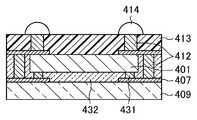
- the solid-state imaging device described in Patent Document 3includes a plurality of silicon substrates 401 each having a photoelectric conversion device region on the lower surface thereof on a transparent adhesive layer 432 on a glass substrate 409 having a size corresponding to a plurality of semiconductor packages. Are bonded apart from each other.
- a connection wiring 407is provided connected to a connection pad 431 made of silicon at and around the lower surface of the silicon substrate 401.
- the silicon substrates 401are cut to obtain a plurality of semiconductor packages each having a photoelectric conversion device region.
- Patent Document 1requires an electrode that penetrates the substrate, and furthermore, an insulating layer, a seed layer, and a conductive layer must be provided, and thus the manufacturing process is complicated.
- the out die image sensor that is a defective productwill be packaged, and the cost of packaging the out die is also included in the packaging cost of the good die that is a good product. End up. As a result, there is a problem that the production cost becomes high.
- Patent Document 2 and Patent Document 3disclose that a resin part is arranged in a peripheral region of the image sensor and a through electrode is formed in the resin part in order to solve the problem associated with the through electrode of the substrate according to Patent Document 1. Yes. However, when the number of pixels is increased and a noise correction function and a signal processing function are added in order to improve the function of the image sensor, the chip size increases and the package size also increases. If the volume of the resin portion disposed in the peripheral region of the image sensor is reduced in order to suppress an increase in the size of the package, the contact area between the resin portion, the glass member, and the peripheral portion of the image sensor is reduced. There is a problem that the reliability of the connection of the through electrode is lowered due to dropping off of the resin portion or the like.
- An object of the present inventionis to solve the above problems and to obtain an optical device that can realize high productivity, high reliability, and downsizing stably and easily.
- the present inventionprovides an optical element (optical chip) having an optical function and a semiconductor element (semiconductor chip) having a peripheral circuit or the like laminated on a transparent member, Is configured to be sealed with a resin material.
- an optical deviceis disposed on an optical element having an optical part on a main surface, a transparent member disposed to face the optical part, and a back surface opposite to the main surface in the optical element.
- a semiconductor elementelectrically connected to the optical element, and a resin portion provided in a peripheral region of the optical element and the semiconductor element on a surface of the transparent member facing the optical element.
- the resin portionmay cover the side surface of the optical element, at least a part of the back surface of the optical element, and the side surface of the semiconductor element.
- the resin portionmay cover the side surface of the optical element, the side surface of the semiconductor element, and a part of the surface opposite to the circuit formation surface in the semiconductor element.
- a first electrodeis provided on the main surface of the optical element, and an external electrode electrically connected to the first electrode is provided on the surface of the resin portion opposite to the transparent member.
- a terminalmay be provided.
- the first electrodeis provided on the main surface of the optical element, and the second electrode is positioned outside the second electrode on the surface of the transparent member facing the optical element.
- a first wiring portionthat electrically connects the second electrode and the third electrode, the first electrode and the second electrode face each other, and the first electrode
- the first projecting electrode disposed between the electrode and the second electrodeis electrically connected, and the first electrically connected to the optical element is disposed outside the optical element and the semiconductor element in the resin portion.
- Through-electrodesone end of the first through-electrode is connected to the third electrode, and the other end of the first through-electrode is disposed on the surface of the resin portion opposite to the transparent member.
- a second wiring portion connected to the portion and an external electrode terminalmay be provided.
- the external electrode terminalmay be provided at a position that does not overlap the semiconductor element in a plan view from the main surface side of the optical element.
- the optical elementmay be a solid-state imaging element.
- the semiconductor elementmay be disposed at the center of the transparent member.
- the back surface of the optical elementis electrically connected to the fourth electrode, the fifth electrode located outside the fourth electrode, and the fourth electrode and the fifth electrode.
- the semiconductor elementis flip-chip connected to the fourth electrode via the second protruding electrode, and one end of the resin portion is connected to the fifth electrode.
- a second penetrating electrodemay be provided.
- the resin constituent material covering the peripheral area of the optical element and the resin constituent material covering the peripheral area of the semiconductor elementmay be the same.
- the resin component material covering the peripheral area of the optical element and the semiconductor element and the resin covering the peripheral area of the first protruding electrodeare formed in the resin portion.
- the constituent materialmay be the same.
- the optical device of the present inventionmay further include a heat radiating member provided on the back surface of the optical element in the resin portion and penetrating the resin portion.
- the heat dissipation membermay have a diameter larger than that of the first through electrode.
- the method of manufacturing an optical deviceincludes a step of forming a first wiring portion having an electrode in each element forming region on a plate-like transparent member including a plurality of element forming regions, and a transparent member.
- a resin partis formed by covering a step of disposing a semiconductor element on a back surface, which is a side surface, and covering a side surface of the optical element and at least a part of the back surface of the optical element and a side surface of the semiconductor element with a resin material.
- a second electrode having an electrode on a surface opposite to the memberA step of forming a line portion and an external electrode terminal electrically connected to the second wiring portion, and a step of cutting the transparent member and the resin portion for each element forming region to separate each of them.
- the step of forming the first through electrodeincludes a heat radiating member that penetrates the resin portion from the surface opposite to the transparent member in the resin portion and is connected to the back surface of the optical element.
- the process of formingmay be included.
- the method for manufacturing an optical device of the present inventionfurther includes a step of forming a third wiring portion having electrodes on the back surface of the optical element before the step of disposing the optical element on the transparent member.
- the semiconductor elementis disposed so as to be electrically connected to the electrode of the third wiring portion, and the step of forming the first through electrode is transparent in the resin portion.
- a step of forming a second through electrode that penetrates the resin portion from the surface opposite to the member and is electrically connected to the electrode of the third wiring portion of the optical elementmay be included.
- the method of manufacturing an optical deviceincludes a step of forming a first wiring portion having an electrode in each element forming region on a plate-like transparent member including a plurality of element forming regions, and a transparent member.
- a step of disposing a plurality of optical elements each having an optical part on the main surface on each element forming region in such a manner that the main surface and the electrode of the first wiring part face each other, opposite to the main surface of the optical elementA step of disposing the semiconductor element on the back surface, which is the side surface, covering the side surface of the optical element, the side surface of the semiconductor element, and a part of the surface of the semiconductor element opposite to the circuit formation surface with a resin material
- the step of forming the resin part and the first through electrode that penetrates the resin part from the surface of the resin part opposite to the transparent member and is electrically connected to the electrode of the first wiring partare formed.
- the method for manufacturing an optical deviceincludes a protruding electrode on the electrode of the first wiring portion between the step of forming the first wiring portion and the step of disposing each optical element on the transparent member. And a step of forming a dam portion that prevents the resin material from flowing into the optical portion around the region of the transparent member that faces the optical portion.
- the constituent material of the dam part and the constituent material of the protruding electrodemay be the same.
- an optical device capable of realizing high productivity, high reliability, and downsizingcan be obtained stably and easily.
- FIG. 1is a cross-sectional view showing the optical device according to the first embodiment.
- FIG. 2is a cross-sectional view showing an optical device according to a first modification of the first embodiment.
- FIG. 3is a cross-sectional view illustrating an optical device according to a second modification of the first embodiment.
- FIG. 4is a cross-sectional view illustrating an optical device according to a third modification of the first embodiment.
- FIG. 5Ais a cross-sectional view in order of steps illustrating the method for manufacturing the optical device according to the first embodiment.
- FIG. 5Bis a cross-sectional view in order of steps illustrating the method for manufacturing the optical device according to the first embodiment.
- FIG. 5Cis a cross-sectional view in order of the steps showing the method for manufacturing the optical device according to the first embodiment.
- FIG. 5Dis a cross-sectional view in order of the steps showing the method of manufacturing the optical device according to the first embodiment.
- FIG. 6Ais a cross-sectional view in order of steps illustrating the method for manufacturing the optical device according to the first embodiment.
- FIG. 6Bis a cross-sectional view in order of the steps, illustrating the method for manufacturing the optical device according to the first embodiment.
- FIG. 6Cis a cross-sectional view in order of the steps showing the method for manufacturing the optical device according to the first embodiment.
- FIG. 6Dis a cross-sectional view in order of the steps, illustrating the method for manufacturing the optical device according to the first embodiment.
- FIG. 6Eis a cross-sectional view in order of the steps, illustrating the method for manufacturing the optical device according to the first embodiment.
- FIG. 7is a cross-sectional view showing an optical device according to the second embodiment.
- FIG. 8Ais a cross-sectional view in order of steps showing the method for manufacturing the optical device according to the second embodiment.
- FIG. 8Bis a cross-sectional view in order of steps showing the method for manufacturing the optical device according to the second embodiment.
- FIG. 8Cis a cross-sectional view in order of steps showing the method for manufacturing the optical device according to the second embodiment.
- FIG. 8Dis a cross-sectional view in order of the steps showing the method of manufacturing the optical device according to the second embodiment.
- FIG. 8Ais a cross-sectional view in order of steps showing the method for manufacturing the optical device according to the second embodiment.
- FIG. 8Bis a cross-sectional view in order of steps showing the method for manufacturing the optical device according to the second embodiment.
- FIG. 9Ais a cross-sectional view in the order of steps showing the method for manufacturing the optical device according to the second embodiment.
- FIG. 9Bis a cross-sectional view in order of steps showing the method for manufacturing the optical device according to the second embodiment.
- FIG. 9Cis a cross-sectional view in order of steps showing the method for manufacturing the optical device according to the second embodiment.
- FIG. 9Dis a cross-sectional view in order of the steps showing the method for manufacturing the optical device according to the second embodiment.
- FIG. 10is a cross-sectional view illustrating a conventional solid-state imaging device.
- FIG. 11is a cross-sectional view showing a solid-state imaging device according to another conventional example.
- FIG. 12is a cross-sectional view showing a solid-state imaging device according to another conventional example.
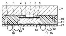
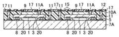
- the optical deviceincludes a transparent member 7 that is a glass material or a resin material that transmits light, an imaging region 1 that is an optical portion on the main surface, and a first electrode 2.
- the image pickup device 3is provided as an optical element, and the semiconductor device 9 is disposed on the back surface opposite to the main surface of the image pickup device 3 and has a circuit surface opposite to the image pickup device 3. .
- the second electrode 4On the surface of the transparent member 7 that faces the main surface of the image sensor 3, the second electrode 4, the third electrode 5 disposed outside the second electrode 4, the second electrode 4, A first wiring portion 6 that electrically connects the three electrodes 5 is provided.
- the first electrode 2 of the imaging element 3is electrically connected to the second electrode 4 provided on the transparent member 7 via the protruding electrode 8.
- the protruding electrode 8may have any form satisfying electrical connection such as gold (Au) or a solder material.
- a plurality of element electrodes 13are provided on the circuit surface of the semiconductor element 9.
- any methodsuch as a die bonding method using a paste-like or sheet-like die-bonding material, or a surface activated bonding by bonding between silicons may be used.
- a die bonding method using a paste-like or sheet-like die-bonding material, or a surface activated bonding by bonding between siliconsmay be used.
- the semiconductor element 9is desirably arranged in accordance with the center position of the optical device, that is, the central portion of the transparent member 7.
- a resin portion 10is provided in the peripheral area between the image sensor 3 and the semiconductor element 9.
- the resin portion 10covers at least a part of the side surface and the back surface of the imaging element 3 and the side surface of the semiconductor element 9.
- the resin material which comprises the resin part 10is dammed in the peripheral part of this imaging area
- the resin portion 10is provided with a plurality of through-electrodes 11 that penetrate the lateral or peripheral regions of the imaging element 3 and the semiconductor element 9 and have one end connected to the third electrode 5 provided on the transparent member 7. It has been.
- “two conductive members are connected”means “a state in which two conductive members are in direct contact”, and “two conductive members are electrically connected”.
- the phrase “being done”includes not only “a state in direct contact” but also “a state in which another conductive member is interposed between two conductive members”.
- a conductive materialsuch as copper (Cu) or a solder material can be used. However, it is not limited to these conductive materials, and other conductive materials may be used.
- a second wiring part 12connected to the other end of each of the plurality of through electrodes 11 and an element connected to the element electrode 13 of the semiconductor element 9.
- a wiring portion 14, an electrode 15 connected to the second wiring portion 12, and, for example, a ball-shaped external electrode terminal 16 formed on the electrode 15are provided.
- a protective resin layer 17is provided on the circuit surface of the semiconductor element 9 and on the surface of the resin portion 10 on the surface opposite to the transparent member 7 except for the second wiring portion 12, the element wiring portion 14 and the external electrode terminal 16. Is provided.
- the imaging element (imaging chip) 3has an imaging function, and the signal processing function from the imaging element 3 and the control function to the imaging element 3 are provided as semiconductor elements.
- (Semiconductor chip) 9is divided into two chips. Further, the two divided chips are stacked, and the two stacked chips are collectively covered with the resin portion 10. With this configuration, it is possible to secure an adhesion area between the imaging element 3 and the semiconductor element 9 of the resin portion 10 formed around the through electrode 11. For this reason, since the effect that it becomes difficult for the resin part 10 to peel from both chips
- the semiconductor element 9 including a circuit portion formed by a fragile fine process aimed at high functionality in the center of an optical element (package) that generates a small amount of stress due to thermal deformation or the likeDamage due to deformation or the like can be avoided. For this reason, a small package with high reliability mounted with a high-performance optical element can be easily realized.
- the circuit portion that has been conventionally arranged around the imaging regionis divided, and the circuit surface is arranged on the external electrode terminal 16 side.
- FIG. 2shows a cross-sectional configuration of an optical device according to a first modification of the first embodiment.
- the adhesion area between the ten image sensors 3 and the semiconductor elements 9can be secured. For this reason, the effect that it becomes difficult to peel the resin part 10 from both the chip
- the semiconductor element 9 including the circuit portionin the central portion of the optical device that generates less stress due to thermal deformation or the like, damage due to thermal deformation or the like can be avoided.
- FIG. 3shows a cross-sectional configuration of an optical device according to a second modification of the first embodiment.
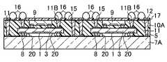
- one terminalis the imaging device 3.
- External electrode terminals 16are respectively provided on the plurality of electrodes 15.
- the through electrode 11 and the heat radiating member 11Acan be formed of a conductive material such as copper (Cu) or a solder material. However, it is not limited to these, and other conductive materials may be used. Further, the heat dissipation member 11 ⁇ / b> A can be further improved in heat dissipation by making the diameter larger than that of the through electrode 11.
- FIG. 4shows a cross-sectional configuration of an optical device according to a third modification of the first embodiment.
- each external electrode terminal 16is arranged in a region directly under the resin portion 10 while avoiding a region directly under the semiconductor element 9.
- the difference in coefficient of thermal expansion between the mounting substrate made of an organic material and the resin portion 10is usually small, the strain stress generated with respect to the change in temperature is relieved. Thereby, the progress of destruction of the external electrode terminal 16 can be prevented, and a small package with high reliability of connection of the external electrode terminal 16 can be easily realized.
- positioned at the back surface of the image pick-up element 3is set to one, it is not limited to this.
- the same effect as that of the first embodimentcan be obtained even when the two semiconductor elements 9 are arranged in parallel on the back surface of the imaging element 3.
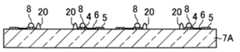
- the second electrode 4 and the third electrode 5are formed on a plate-like transparent member 7A including a plurality of element forming regions corresponding to a plurality of optical devices. More specifically, a physical vapor deposition (PVD) method, for example, sputtering, is used to form titanium tungsten (TiW), aluminum (Al), copper (Cu) on the entire surface of the transparent member 7A. ) Or nickel (Ni) or other seed metal layer. Subsequently, the seed metal layer is patterned into a plurality of electrodes by lithography and etching. Subsequently, the metal layer is formed on the patterned seed metal layer by plating to form the electrodes 4, 5 and the first wiring portion 6.
- PVDphysical vapor deposition
- each of the electrodes 4 and 5can be made larger than that of the dam portion by masking the formation region of the plurality of dam portions to be formed in a later process with a resist film or the like.
- goldAu
- Sputteringcan be used to form this metal layer, but electrolytic plating is more advantageous for mass production.
- a dam portion 20is formed in a region facing the periphery of the imaging region in the imaging device.
- projecting electrodes 8 for connection to the image sensorare formed on the respective second electrodes 4. It is desirable that the dam portion 20 and the protruding electrode 8 are formed of the same member and at the same time.
- a solder materialmay be plated on Cu or Ni, or a stud bump made of Au may be formed.
- the protruding electrode 8may be formed on the first electrode formed on the imaging element by a stud bump method or the like.
- the image sensor 3is connected to the transparent member 7A by a flip chip bonding method.
- the protruding electrode 8 on the second electrode 4 and the first electrode 2 of the image sensor 3are connected to each other. Further, only the non-defective image sensor 3 can be selected and bonded as the image sensor 3 to be mounted. As a result, production costs can be reduced. Further, at this time, an underfill material may be filled in an outer portion of the dam portion 20 in a region facing the transparent member 7A of the image sensor 3. This makes it possible to select materials that are suitable for the protection of the connecting portion made of the protruding electrodes 8 and the protection of the image sensor 3.
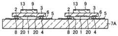
- the semiconductor element 9is fixed on the back surface of the image sensor 3 with the surface opposite to the circuit surface thereof facing.
- a resinis formed on the main surface of the transparent member 7A, between the main surface of the transparent member 7A and the image sensor 3, and on the side of the image sensor 3 and the semiconductor element 9. Cover with lump 10A.
- a filling method of the resin material 10Athere is a compression molding method or a transfer mold method, or a method of applying the resin material 10A in a plurality of island shapes and spreading and filling by a capillary phenomenon. An appropriate method can be selected depending on the wet spreading property.
- the dam portion 20is formed between the protruding electrode 8 that is a connecting portion between the imaging element 3 and the transparent member 7 ⁇ / b> A and the imaging region 1.
- the dam part 20remains as it is after the manufacturing.
- the dam portion 20having the same configuration as the present configuration, the same applies to the embodiment.
- the resin material 10Ais made of, for example, an insulating epoxy resin to which a filler such as silica is added.
- a plurality of through electrodes 11are formed in the resin material 10A.
- etching the opening for forming the through electrode 11For example, there are a method of forming an opening by a laser beam, a method of forming an opening by a reactive ion etching (RIE) method, a method of exposing by masking with a photosensitive resin material, and the like.
- RIEreactive ion etching
- a heat radiating member 11A connected to the back surface of the image sensor 3may be formed.
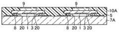
- a plurality of electrodes 15are respectively formed on a predetermined position on the resin material 10A and on the heat radiation member 11A. Subsequently, the second wiring portion 12 is formed on the through electrode 11. Thereafter, a protective resin layer 17 is formed on the resin material 10A in the region excluding the electrode 15 and insulated.
- each external electrode terminal 16is desirably disposed on the resin material 10 ⁇ / b> A so as not to overlap the element formation surface of the semiconductor element 9.
- the resin material 10A and the transparent member 7Aare diced so as to include one element formation region, that is, one optical device, and are separated into individual pieces.
- the transparent member 7is obtained from the transparent member 7A
- the resin portion 10is obtained from the resin material 10A, so that a desired optical device can be obtained.
- the heat radiating member 11A shown in the step of FIG. 6Cis not necessarily formed. If the heat radiating member 11A is not formed, an optical device having the configuration shown in FIG. 1 can be obtained.
- the image pickup element 3 including the image pickup function and the semiconductor element 9 including the peripheral circuit functionare divided, these at least two chips are stacked, and further covered with the resin material 10A all together. .
- the adhesion area with the image pick-up element 3 and the semiconductor element 9 of 10 A of resin materials in which the penetration electrode 11 was formedis securable. For this reason, since peeling of the resin material 10A from the imaging element 3 and the semiconductor element 9 is suppressed, it is possible to easily realize downsizing of the optical device without deteriorating the connection reliability of the through electrode 11. .
- the semiconductor element 9 including the circuit part formed by a fragile micro process for the purpose of high functionalityin the center part of the package where the stress generated by thermal deformation or the like is small, damage due to thermal deformation or the like Can be avoided. For this reason, a small package with high reliability mounted with a high-performance optical element can be easily realized.
- the external electrode terminal 16can be arranged so as not to overlap the semiconductor element 9 in a plan view from above the main surface of the transparent member 7A.
- the mounting substrate made of an organic materialusually has a small difference in thermal expansion coefficient from the resin material 10A, so that the strain stress generated by the temperature change is relieved. For this reason, the progress of destruction of the external electrode terminal 16 is prevented, and a small package with high reliability of connection of the external electrode terminal 16 can be easily realized.
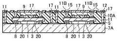
- the optical device according to the present embodimentis positioned on the back surface, which is the surface opposite to the imaging region 1 in the imaging device 3, on the fourth electrode 22 and outside the fourth electrode 22.
- a fifth electrode 23 and a third wiring portion 24 that electrically connects the fourth electrode 22 and the fifth electrode 23are provided.
- the semiconductor element 9is flip-chip connected to the fourth electrode 22 via the protruding electrode 8 on the element electrode 13.
- the protruding electrode 8may be in any form satisfying electrical connection such as gold (Au) or a solder material.
- the fifth electrode 23 of the imaging device 3is connected to one end of the through electrode 11B that penetrates the resin portion 10.
- the other end of the through electrode 11Bis connected to an electrode 15 formed on the back surface of the resin portion 10.
- the through electrodes 11 and 11Bare formed of a conductive material such as copper (Cu) or a solder material. However, it is not limited to these, and other conductive materials may be used.
- each external electrode terminal 16can be arranged on the back surface of the resin portion 10 at equal intervals. At this time, each external electrode terminal 16 is desirably disposed on the resin portion 10 so as not to overlap the semiconductor element 9 in plan view.
- the imaging element (imaging chip) 3has an imaging function, and the signal processing function from the imaging element 3 and the control function to the imaging element 3 are provided as semiconductor elements.
- (Semiconductor chip) 9is divided into two chips. Further, the two divided chips are stacked, and the two stacked chips are collectively covered with the resin portion 10. With this configuration, it is possible to secure an adhesion area between the imaging element 3 and the semiconductor element 9 of the resin portion 10 formed around the through electrode 11. For this reason, since the effect that it becomes difficult for the resin part 10 to peel from both chips
- the semiconductor element 9 including a circuit portion formed by a fragile fine process aimed at high functionality in the center of an optical element (package) that generates a small amount of stress due to thermal deformation or the likeDamage due to deformation or the like can be avoided. For this reason, a small package with high reliability mounted with a high-performance optical element can be easily realized.
- each external electrode terminal 16is disposed in a region directly under the resin portion 10 while avoiding a region directly under the semiconductor element 9. If it does in this way, since the difference of the thermal expansion coefficient of the mounting substrate which consists of organic materials, and the resin part 10 is small normally, the distortion stress which generate
- one semiconductor element 9is provided on the back surface of the image sensor 3, but the present invention is not limited to this.
- the same effect as that of the first embodimentcan be obtained even in a structure in which two or more semiconductor elements 9 are arranged in parallel on the back surface of the imaging element 3.
- the second electrode 4 and the third electrode 5are formed on a plate-like transparent member 7A including a plurality of element forming regions corresponding to a plurality of optical devices. More specifically, a seed metal layer such as TiW, Al, Cu, or Ni is formed on the entire surface of the transparent member 7A using a PVD method, for example, a sputtering method. Subsequently, the seed metal layer is patterned into a plurality of electrodes by lithography and etching. Subsequently, the metal layer is formed on the patterned seed metal layer by plating to form the electrodes 4, 5 and the first wiring portion 6.
- a seed metal layersuch as TiW, Al, Cu, or Ni is formed on the entire surface of the transparent member 7A using a PVD method, for example, a sputtering method.
- the seed metal layeris patterned into a plurality of electrodes by lithography and etching.
- the metal layeris formed on the patterned seed metal layer by plating to form the electrodes 4,
- the height of each of the electrodes 4 and 5can be made larger than that of the dam portion by masking the formation region of the plurality of dam portions to be formed in a later process with a resist film or the like.
- Auis generally formed on Ni. Sputtering can be used to form this metal layer, but electrolytic plating is more advantageous for mass production.
- a dam portion 20is formed in a region facing the periphery of the imaging region in the imaging device.
- projecting electrodes 8 for connection to the image sensorare formed on the respective second electrodes 4. It is desirable that the dam portion 20 and the protruding electrode 8 are formed of the same member and are formed simultaneously.
- a solder materialmay be plated on Cu or Ni, or a stud bump made of Au may be formed.
- the protruding electrode 8may be formed on the first electrode formed on the imaging element by a stud bump method or the like.
- the image sensor 3is connected to the transparent member 7A by a flip chip bonding method.
- the protruding electrode 8 on the second electrode 4 in the transparent member 7A and the first electrode 2 of the imaging element 3are connected to each other. Further, only the non-defective image sensor 3 can be selected and bonded as the image sensor 3 to be mounted. As a result, production costs can be reduced.
- a fourth electrode 22, a fifth electrode 23, and a third wiring portion 24 for connecting themare connected in advance to a semiconductor device to be mounted in a later process. Is formed.
- the electrodes 22 and 23 and the third wiring portion 24are formed in a wafer state before the semiconductor elements are separated.
- the formation methodis the same as the electrodes 4 and 5 and the first wiring portion 6 formed on the transparent member 7A, by formation of a seed metal layer using TiW, Al, Cu, Ni or the like by sputtering, or by etching. Patterning of the seed metal layer and formation of the metal layer by plating are performed.
- an underfill materialmay be filled in an outer portion of the dam portion 20 in a region facing the transparent member 7A of the image pickup device 3. Good. This makes it possible to select materials that are suitable for the protection of the connecting portion made of the protruding electrodes 8 and the protection of the image sensor 3.
- the semiconductor element 9is connected to the back surface of the imaging element 3 by a flip chip bonding method through the protruding electrodes 8.
- This joining methodmay be any joining method such as Au—Au joining or solder joining, and is not particularly limited.
- a resinis formed on the main surface of the transparent member 7A, between the main surface of the transparent member 7A and the image sensor 3, and on the side of the image sensor 3 and the semiconductor element 9. Cover with lump 10A.
- a filling method of the resin material 10Athere are a compression molding method or a transfer mold method, or a method of applying the resin material 10A in a plurality of island shapes and spreading and filling by a capillary phenomenon. An appropriate method can be selected depending on the spread.
- the dam portion 20is formed between the protruding electrode 8 that is a connecting portion between the imaging element 3 and the transparent member 7 ⁇ / b> A and the imaging region 1. Thereby, the penetration
- the surface of the resin material 10A and the back surface of each semiconductor element 9 exposed from the resin material 10Aare polished by a back-grinding method or a chemical mechanical polishing (CMP) method, etc., to further reduce the thickness of the optical device. You may plan.
- CMPchemical mechanical polishing
- a plurality of through electrodes 11 and 11Bare formed in the resin material 10A.
- a through electrode 11 connected to the third electrode 5 on the transparent member 7A and a through electrode 11B connected to the fifth electrode 23 on the back surface of the imaging element 3are formed.
- the method for etching the openings for forming the through electrodes 11 and 11Bincludes, for example, a method of forming the openings by laser light or RIE, or a method of exposing by masking with a photosensitive resin material. is there.
- electrodes 15are selectively formed on the resin material 10A and on the through electrodes 11 and 11B, respectively. Thereafter, a protective resin layer 17 is formed on the resin material 10A in the region excluding the electrode 15 and insulated.
- each external electrode terminal 16is preferably disposed on the resin material 10 ⁇ / b> A so as not to overlap the element formation surface of the semiconductor element 9.
- the resin material 10A and the transparent member 7Aare diced so as to include one element formation region, that is, one optical device, and are separated into individual pieces.
- the transparent member 7is obtained from the transparent member 7A
- the resin portion 10is obtained from the resin material 10A, so that a desired optical device can be obtained.
- the image pickup element 3 including the image pickup function and the semiconductor element 9 including the peripheral circuit functionare divided, these at least two chips are stacked, and further covered with the resin material 10A all together. .
- the adhesion area with the image pick-up element 3 and the semiconductor element 9 of 10 A of resin materials in which the penetration electrode 11 was formedis securable. For this reason, since peeling of the resin material 10A from the imaging element 3 and the semiconductor element 9 is suppressed, it is possible to easily realize downsizing of the optical device without deteriorating the connection reliability of the through electrode 11. .
- the semiconductor element 9 including the circuit part formed by a fragile micro process for the purpose of high functionalityin the center part of the package where the stress generated by thermal deformation or the like is small, damage due to thermal deformation or the like Can be avoided. For this reason, a small package with high reliability mounted with a high-performance optical element can be easily realized.
- the external electrode terminal 16can be arranged so as not to overlap the semiconductor element 9 in a plan view from above the main surface of the transparent member 7A.
- the mounting substrate made of an organic materialusually has a small difference in thermal expansion coefficient from the resin material 10A, so that the strain stress generated by the temperature change is relieved. For this reason, the progress of destruction of the external electrode terminal 16 is prevented, and a small package with high reliability of connection of the external electrode terminal 16 can be easily realized.
- the image pickup devicesolid-state image pickup device
- the optical deviceLD
- an optical elementsuch as a light receiving element
- the electrical connection between the first electrode 2 provided on the main surface of the optical element 3 and the external electrode terminal 16 provided on the resin portionis not limited to means using the through electrode 11.
- the first wiring portion 6is formed up to the side end portion of the transparent member 7
- the second wiring portion 12is also formed up to the side end portion of the resin portion 10, and a conductor connecting both is formed on the side end surface of the resin portion 10.
- This configurationcan reduce the width of the optical device and enables downsizing as compared with the configuration in which the third electrode 5 and the through electrode 11 are provided outside the optical element 3.
- optical device and the manufacturing method thereof according to the present inventionare useful for a light-emitting element or a light-receiving element used in a digital optical device or the like.
- Imaging area(optical part) 2 First electrode 3 Imaging element (optical element) 4 Second electrode 5 Third electrode 6 First wiring part 7, 7A Transparent member 8 Projection electrode 9 Semiconductor element 10 Resin part 10A Resin material 11, 11B Through electrode 11A Heat radiation member 12 Second wiring part 13 Element Electrode 14 Element wiring portion 15 Electrode 16 External electrode terminal 17 Protective resin layer 20 Dam portion 22 Fourth electrode 23 Fifth electrode 24 Third wiring portion
Landscapes
- Engineering & Computer Science (AREA)
- Computer Hardware Design (AREA)
- Microelectronics & Electronic Packaging (AREA)
- Power Engineering (AREA)
- Manufacturing & Machinery (AREA)
- Solid State Image Pick-Up Elements (AREA)
- Structures Or Materials For Encapsulating Or Coating Semiconductor Devices Or Solid State Devices (AREA)
- Transforming Light Signals Into Electric Signals (AREA)
- Wire Bonding (AREA)
Abstract
Description
Translated fromJapanese本発明は、光学装置及びその製造方法に関する。The present invention relates to an optical device and a manufacturing method thereof.
スマートフォン及びタブレット機器の小型化の要望から、それらに搭載されるCCD(Charge Coupled Device)又はCMOS(Complementary Metal-Oxide Semiconductor)からなる固体撮像素子は、近年益々小型化が要求されている。Due to demands for miniaturization of smartphones and tablet devices, solid-state imaging devices composed of CCD (Charge Coupled Device) or CMOS (Complementary Metal-Oxide Semiconductor) mounted on them are increasingly required to be miniaturized in recent years.
これらの小型化の要求に答えるには、従来のセラミックパッケージ及び樹脂モールドパッケージでは対応が困難であり、小型のパッケージングを行える固体撮像装置が提案されている(例えば、特許文献1、2及び3を参照。)。In order to meet these demands for miniaturization, conventional ceramic packages and resin mold packages are difficult to cope with, and solid-state imaging devices capable of small packaging have been proposed (for example,
図10は特許文献1に記載された固体撮像装置の断面構成を示している。特許文献1に記載の固体撮像装置は、基板202と、基板202の第一の表面202a上又は基板202の内部に設けられた電子部品203と、電子部品203に電気的に接続されていると共に基板202の第一の表面202a上に設けられた接続電極204と、接続電極204の裏面に達するように基板202の厚さ方向に貫通する第一の貫通孔部205と、第一の貫通孔部205の内部に設けられていると共に第一の貫通孔部205の内部から基板202の第二の表面202b上へ延びるように設けられた貫通電極206と、基板202の第二の表面202b上に設けられ、基板202の第二の表面202b上において貫通電極206と電気的に接続された配線電極207と、配線電極207の表面を覆うように基板202の第二の表面202b上に設けられた絶縁層208とを備えている。FIG. 10 shows a cross-sectional configuration of the solid-state imaging device described in
図11は特許文献2に記載された固体撮像装置の断面構成を示している。特許文献2に記載の固体撮像装置は、デジタル器機等に用いられるウェーハレベルのイメージセンサモジュール301において、イメージセンサに流入される光から特定波長の光を除去する光学フィルタ310、光学フィルタ310に付着されてフィルタ用コーティング層310aを保護し、その後面には複数のパッド電極330が形成されるガラス層320、ガラス層320のパッド電極330に付着され、パッド電極330からその後面に再分配パッド342が形成されるイメージセンサ、及び該イメージセンサの後面側に配置され、パッド電極330に電気的に連結されるソルダボール370を含んでいる。イメージセンサの外側は樹脂層350で覆われており、樹脂層350には複数のビアホール352が形成され、ビアホール352には導電性材料が充填又はめっき処理されてパッド電極330と再分配パッド342とを電気的に連結している。FIG. 11 shows a cross-sectional configuration of the solid-state imaging device described in
図12は特許文献3に記載された固体撮像装置の断面構成を示している。特許文献3に記載の固体撮像装置は、複数の半導体パッケージに対応するサイズを持つガラス基板409上の透明接着層432の上には、それぞれが下面に光電変換デバイス領域を有する複数のシリコン基板401が相互に離間して接着されている。シリコン基板401の下面周辺部及びその周囲には、接続用配線407がシリコンからなる接続パッド431に接続されて設けられている。絶縁膜、再配線、柱状電極412、封止膜413及び半田ボール414を順次形成した後に、シリコン基板401同士の間で切断し、それぞれが光電変換デバイス領域を備えた複数の半導体パッケージを得る。FIG. 12 shows a cross-sectional configuration of the solid-state imaging device described in
しかしながら、特許文献1に記載された方法は、基板を貫通する電極が必要であり、さらに、絶縁層、シード層及び導電層を設けなければならないため、その製造工程が複雑となる。また、貫通電極を設ける電極の下側には、配線及びトランジスタ素子を配置することができないという設計上の制約があり、撮像素子チップに特殊な設計が必要となる。このため、設計コストが増大し、また、仕様変更に対して柔軟に対応ができないという問題がある。さらに、生産過程において、不良品であるアウトダイ(Out Die)のイメージセンサまでパッケージングすることになり、該アウトダイをパッケージングする費用も良品であるグッドダイ(Good Die)のパッケージング費用に含まれてしまう。その結果、生産原価が高くなるという問題がある。However, the method described in
また、特許文献2及び特許文献3は、特許文献1に係る基板の貫通電極に伴う問題を解決するため、撮像素子の周辺領域に樹脂部を配置し、該樹脂部内に貫通電極を形成している。しかし、撮像素子の機能を向上するために、画素数を増加すると共にノイズ補正機能及び信号処理機能等を追加した場合には、チップサイズが大きくなり、パッケージのサイズも大きくなってしまう。パッケージのサイズの増加を抑えるために、撮像素子の周辺領域に配置される樹脂部の体積を小さくしてしまうと、該樹脂部とガラス部材及び撮像素子の周辺部との密着面積が少なくなるため、樹脂部の脱落等による貫通電極の接続の信頼性が低下するという問題がある。
本発明は、上記の問題を解決し、高生産性、高信頼性及び小型化を実現できる光学装置を安定且つ容易に得られるようにすることを目的とする。An object of the present invention is to solve the above problems and to obtain an optical device that can realize high productivity, high reliability, and downsizing stably and easily.
上記の目的を達成するため、本発明は、光学機能を備えた光学素子(光学チップ)と、周辺回路等を備えた半導体素子(半導体チップ)とを透明部材上に積層し、両チップの周囲を樹脂材によって封止する構成とする。In order to achieve the above object, the present invention provides an optical element (optical chip) having an optical function and a semiconductor element (semiconductor chip) having a peripheral circuit or the like laminated on a transparent member, Is configured to be sealed with a resin material.
具体的に、本発明に係る光学装置は、主面に光学部を有する光学素子と、光学部と対向して配置された透明部材と、光学素子における主面と反対側の裏面上に配置され、光学素子と電気的に接続された半導体素子と、透明部材における光学素子と対向する面上で、光学素子と半導体素子との周辺領域に設けられた樹脂部とを備えている。Specifically, an optical device according to the present invention is disposed on an optical element having an optical part on a main surface, a transparent member disposed to face the optical part, and a back surface opposite to the main surface in the optical element. A semiconductor element electrically connected to the optical element, and a resin portion provided in a peripheral region of the optical element and the semiconductor element on a surface of the transparent member facing the optical element.
本発明の光学装置において、樹脂部は、光学素子の側面と、光学素子の裏面の少なくとも一部と、半導体素子の側面とを覆っていてもよい。In the optical device of the present invention, the resin portion may cover the side surface of the optical element, at least a part of the back surface of the optical element, and the side surface of the semiconductor element.
本発明の光学装置において、樹脂部は、光学素子の側面と、半導体素子の側面と、半導体素子における回路形成面と反対側の面の一部とを覆っていてもよい。In the optical device of the present invention, the resin portion may cover the side surface of the optical element, the side surface of the semiconductor element, and a part of the surface opposite to the circuit formation surface in the semiconductor element.
本発明の光学装置において、光学素子の主面には、第1の電極が設けられ、樹脂部における透明部材と反対側の面上には、第1の電極と電気的に接続された外部電極端子とが設けられていてもよい。In the optical device of the present invention, a first electrode is provided on the main surface of the optical element, and an external electrode electrically connected to the first electrode is provided on the surface of the resin portion opposite to the transparent member. A terminal may be provided.
本発明の光学装置において、光学素子の主面には、第1の電極が設けられ、透明部材における光学素子と対向する面上には、第2の電極、該第2の電極の外側に位置する第3の電極、及び第2の電極と第3の電極とを電気的に接続する第1の配線部が設けられ、第1の電極と第2の電極とは互いに対向し、第1の電極と第2の電極との間に配された第1の突起電極により電気的に接続され、樹脂部における光学素子及び半導体素子の外方には、光学素子と電気的に接続された第1の貫通電極が設けられ、第1の貫通電極の一方の端部は、第3の電極と接続され、樹脂部における透明部材と反対側の面上には、第1の貫通電極の他方の端部と接続された第2の配線部と外部電極端子とが設けられていてもよい。In the optical device of the present invention, the first electrode is provided on the main surface of the optical element, and the second electrode is positioned outside the second electrode on the surface of the transparent member facing the optical element. And a first wiring portion that electrically connects the second electrode and the third electrode, the first electrode and the second electrode face each other, and the first electrode The first projecting electrode disposed between the electrode and the second electrode is electrically connected, and the first electrically connected to the optical element is disposed outside the optical element and the semiconductor element in the resin portion. Through-electrodes, one end of the first through-electrode is connected to the third electrode, and the other end of the first through-electrode is disposed on the surface of the resin portion opposite to the transparent member. A second wiring portion connected to the portion and an external electrode terminal may be provided.
この場合に、外部電極端子は、光学素子の主面側からの平面視において、半導体素子と重ならない位置に設けられていてもよい。In this case, the external electrode terminal may be provided at a position that does not overlap the semiconductor element in a plan view from the main surface side of the optical element.
本発明の光学装置において、光学素子は、固体撮像素子であってもよい。In the optical device of the present invention, the optical element may be a solid-state imaging element.
本発明の光学装置において、半導体素子は、透明部材の中央部に配置されていてもよい。In the optical device of the present invention, the semiconductor element may be disposed at the center of the transparent member.
本発明の光学装置において、光学素子の裏面には、第4の電極、該第4の電極の外側に位置する第5の電極、及び第4の電極と第5の電極とを電気的に接続する第3の配線部が設けられ、半導体素子は、第2の突起電極を介して第4の電極とフリップチップ接続されており、樹脂部には、一方の端部が第5の電極と接続された第2の貫通電極が設けられていてもよい。In the optical device of the present invention, the back surface of the optical element is electrically connected to the fourth electrode, the fifth electrode located outside the fourth electrode, and the fourth electrode and the fifth electrode. The semiconductor element is flip-chip connected to the fourth electrode via the second protruding electrode, and one end of the resin portion is connected to the fifth electrode. A second penetrating electrode may be provided.
本発明の光学装置において、樹脂部において、光学素子の周辺の領域を覆う樹脂の構成材料と半導体素子の周辺の領域を覆う樹脂の構成材料とは、同一であってもよい。In the optical device of the present invention, in the resin portion, the resin constituent material covering the peripheral area of the optical element and the resin constituent material covering the peripheral area of the semiconductor element may be the same.
本発明の光学装置において、第1の突起電極を有する場合に、樹脂部において、光学素子及び半導体素子の周辺の領域を覆う樹脂の構成材料と第1の突起電極の周辺の領域を覆う樹脂の構成材料とは、同一であってもよい。In the optical device of the present invention, when the first protruding electrode is provided, the resin component material covering the peripheral area of the optical element and the semiconductor element and the resin covering the peripheral area of the first protruding electrode are formed in the resin portion. The constituent material may be the same.
本発明の光学装置は、樹脂部における光学素子の裏面に設けられ、樹脂部を貫通する放熱用部材をさらに備えていてもよい。The optical device of the present invention may further include a heat radiating member provided on the back surface of the optical element in the resin portion and penetrating the resin portion.
この場合に、放熱用部材は、第1の貫通電極よりも径が大きくてもよい。In this case, the heat dissipation member may have a diameter larger than that of the first through electrode.
本発明に係る光学装置の製造方法は、複数の素子形成領域を含む板状の透明部材の上に、各素子形成領域のそれぞれに電極を有する第1の配線部を形成する工程と、透明部材の各素子形成領域の上に、それぞれ主面に光学部を有する複数の光学素子を主面と第1の配線部の電極とをそれぞれ対向させて配置する工程と、光学素子における主面と反対側の面である裏面上に、半導体素子を配置する工程と、光学素子の側面及び該光学素子の裏面の少なくとも一部と半導体素子の側面とを樹脂材により覆うことにより、樹脂部を形成する工程と、樹脂部の透明部材と反対側の面から樹脂部を貫通して、第1の配線部の電極と電気的に接続される第1の貫通電極を形成する工程と、樹脂部における透明部材と反対側の面上に、電極を有する第2の配線部と、該第2の配線部と電気的に接続される外部電極端子とを形成する工程と、各素子形成領域ごとに、透明部材及び樹脂部を切断して、それぞれ個片化する工程とを備えている。The method of manufacturing an optical device according to the present invention includes a step of forming a first wiring portion having an electrode in each element forming region on a plate-like transparent member including a plurality of element forming regions, and a transparent member. A step of disposing a plurality of optical elements each having an optical part on the main surface on each element forming region in such a manner that the main surface and the electrode of the first wiring part face each other, opposite to the main surface of the optical element A resin part is formed by covering a step of disposing a semiconductor element on a back surface, which is a side surface, and covering a side surface of the optical element and at least a part of the back surface of the optical element and a side surface of the semiconductor element with a resin material. A step of forming a first through electrode that is electrically connected to the electrode of the first wiring portion by penetrating the resin portion from the surface of the resin portion opposite to the transparent member, and transparent in the resin portion A second electrode having an electrode on a surface opposite to the member; A step of forming a line portion and an external electrode terminal electrically connected to the second wiring portion, and a step of cutting the transparent member and the resin portion for each element forming region to separate each of them. And.
本発明の光学装置の製造方法において、第1の貫通電極を形成する工程は、樹脂部における透明部材と反対側の面から樹脂部を貫通して、光学素子の裏面と接続される放熱用部材を形成する工程を含んでいてもよい。In the method of manufacturing an optical device of the present invention, the step of forming the first through electrode includes a heat radiating member that penetrates the resin portion from the surface opposite to the transparent member in the resin portion and is connected to the back surface of the optical element. The process of forming may be included.
本発明の光学装置の製造方法は、光学素子を透明部材の上に配置する工程よりも前に、光学素子の裏面上に電極を有する第3の配線部を形成する工程をさらに備え、光学素子の裏面上に半導体素子を配置する工程において、半導体素子は、第3の配線部の電極と電気的に接続されるように配置し、第1の貫通電極を形成する工程は、樹脂部における透明部材と反対側の面から樹脂部を貫通して、光学素子の第3の配線部の電極と電気的に接続される第2の貫通電極を形成する工程を含んでいてもよい。The method for manufacturing an optical device of the present invention further includes a step of forming a third wiring portion having electrodes on the back surface of the optical element before the step of disposing the optical element on the transparent member. In the step of disposing the semiconductor element on the back surface of the substrate, the semiconductor element is disposed so as to be electrically connected to the electrode of the third wiring portion, and the step of forming the first through electrode is transparent in the resin portion. A step of forming a second through electrode that penetrates the resin portion from the surface opposite to the member and is electrically connected to the electrode of the third wiring portion of the optical element may be included.
本発明に係る光学装置の製造方法は、複数の素子形成領域を含む板状の透明部材の上に、各素子形成領域のそれぞれに電極を有する第1の配線部を形成する工程と、透明部材の各素子形成領域の上に、それぞれ主面に光学部を有する複数の光学素子を主面と第1の配線部の電極とをそれぞれ対向させて配置する工程と、光学素子における主面と反対側の面である裏面上に、半導体素子を配置する工程と、光学素子の側面と、半導体素子の側面と、半導体素子における回路形成面と反対側の面の一部とを樹脂材により覆うことにより、樹脂部を形成する工程と、樹脂部の透明部材と反対側の面から樹脂部を貫通して、第1の配線部の電極と電気的に接続される第1の貫通電極を形成する工程と、樹脂部における透明部材と反対側の面上に、電極を有する第2の配線部と、第2の配線部と電気的に接続される外部電極端子とを形成する工程と、各素子形成領域ごとに、透明部材及び樹脂部を切断して、それぞれ個片化する工程とを備えている。The method of manufacturing an optical device according to the present invention includes a step of forming a first wiring portion having an electrode in each element forming region on a plate-like transparent member including a plurality of element forming regions, and a transparent member. A step of disposing a plurality of optical elements each having an optical part on the main surface on each element forming region in such a manner that the main surface and the electrode of the first wiring part face each other, opposite to the main surface of the optical element A step of disposing the semiconductor element on the back surface, which is the side surface, covering the side surface of the optical element, the side surface of the semiconductor element, and a part of the surface of the semiconductor element opposite to the circuit formation surface with a resin material The step of forming the resin part and the first through electrode that penetrates the resin part from the surface of the resin part opposite to the transparent member and is electrically connected to the electrode of the first wiring part are formed. On the surface of the resin part opposite to the transparent member, A step of forming a second wiring portion having external electrodes and an external electrode terminal electrically connected to the second wiring portion, and cutting the transparent member and the resin portion for each element forming region, And a step of separating.
本発明の光学装置の製造方法は、第1の配線部を形成する工程と、透明部材の上に各光学素子を配置する工程との間に、第1の配線部の電極の上に突起電極を形成すると共に、透明部材における光学部と対向する領域の周囲に、樹脂材の光学部上への流入を阻止するダム部を形成する工程をさらに備えていてもよい。The method for manufacturing an optical device according to the present invention includes a protruding electrode on the electrode of the first wiring portion between the step of forming the first wiring portion and the step of disposing each optical element on the transparent member. And a step of forming a dam portion that prevents the resin material from flowing into the optical portion around the region of the transparent member that faces the optical portion.
この場合に、ダム部の構成材料と突起電極の構成材料とは、同一であってもよい。In this case, the constituent material of the dam part and the constituent material of the protruding electrode may be the same.
本発明に係る光学装置及びその製造方法によると、高生産性、高信頼性及び小型化を実現できる光学装置を安定且つ容易に得ることができる。According to the optical device and the manufacturing method thereof according to the present invention, an optical device capable of realizing high productivity, high reliability, and downsizing can be obtained stably and easily.
(第1の実施形態)
第1の実施形態に係る光学装置について図1を参照しながら説明する。(First embodiment)
The optical device according to the first embodiment will be described with reference to FIG.
図1に示すように、本実施形態に係る光学装置は、光を透過するガラス材又は樹脂材である透明部材7と、主面に光学部である撮像領域1と第1の電極2とが設けられた光学素子としての撮像素子3と、撮像素子3における主面と反対側の裏面上に配置され、回路面を撮像素子3と反対側の面とする半導体素子9とから構成されている。As shown in FIG. 1, the optical device according to the present embodiment includes a
透明部材7における撮像素子3の主面と対向する面上には、第2の電極4、該第2の電極4の外側に配置される第3の電極5、及び第2の電極4と第3の電極5とを電気的に接続する第1の配線部6が設けられている。撮像素子3の第1の電極2は、透明部材7に設けられた第2の電極4との間で突起電極8を介して電気的に接続されている。突起電極8は、金(Au)又ははんだ材等の電気的な接続を満たす、いずれの形態であってもよい。On the surface of the
半導体素子9の回路面には、複数の素子電極13が設けられている。A plurality of
半導体素子9と撮像素子3とを固着するには、ペースト状若しくはシート状のダイボンド材を用いたダイスボンド工法、又はシリコン同士の結合による表面活性化接合等のいずれの方法を用いてもよい。また、半導体素子9の撮像素子3の裏面上への配置位置に制約はなく、任意に配置することができる。なお、半導体素子9は、光学装置の中心位置、すなわち透明部材7の中央部に合わせて配置することが望ましい。In order to fix the
透明部材7における撮像素子3との対向面上で、撮像素子3と半導体素子9との周辺領域には樹脂部10が設けられている。樹脂部10は、撮像素子3の側面及びその裏面の少なくとも一部と、半導体素子9の側面とを覆っている。なお、樹脂部10を構成する樹脂材は、撮像素子3の主面に設けられた撮像領域1を覆わないように、該撮像領域1の周辺部で堰き止められる。この堰き止め方法の一例を後述する。On the surface of the
樹脂部10には、撮像素子3及び半導体素子9の側方又は周囲の領域を貫通し、その一端が透明部材7に設けられた第3の電極5と接続された複数の貫通電極11が設けられている。なお、本願明細書においては、「2つの導電性部材が接続されている」とは、「2つの導電性部材が直接に接した状態」をいい、「2つの導電性部材が電気的に接続されている」とは、「直接に接した状態」だけでなく「2つの導電性部材の間に他の導電性部材が介在した状態」をも含めていう。貫通電極11には、銅(Cu)又ははんだ材等の導電性材料を用いることができる。但し、これらの導電性材料に限定されず、他の導電性材料であってもよい。The
樹脂部10における透明部材7と反対側の面上には、複数の貫通電極11のそれぞれの他端と接続される第2の配線部12と、半導体素子9の素子電極13と接続される素子配線部14と、第2の配線部12と接続される電極15と、該電極15の上に形成された、例えばボール状の外部電極端子16とが設けられている。On the surface of the
半導体素子9の回路面上、並びに樹脂部10における透明部材7と反対側の面上の第2の配線部12、素子配線部14及び外部電極端子16を除く領域には、保護樹脂層17が設けられている。A
このように、第1の実施形態に係る光学装置は、撮像素子(撮像チップ)3には撮像機能を持たせ、撮像素子3からの信号処理機能及び撮像素子3への制御機能等を半導体素子(半導体チップ)9に持たせて、2つのチップに分割していている。さらに、分割した2つのチップを積層し、積層された2つのチップを樹脂部10によって一括に覆っている。この構成により、貫通電極11の周辺に形成される樹脂部10の撮像素子3及び半導体素子9との接着面積を確保することができる。このため、樹脂部10が両チップから剥離しにくくなるという効果を得られるので、貫通電極11の接続の信頼性を低下させることなく、光学装置の小型化を容易に実現することができる。As described above, in the optical device according to the first embodiment, the imaging element (imaging chip) 3 has an imaging function, and the signal processing function from the
また、高機能化を目的とした脆弱な微細プロセスによって形成される回路部を含む半導体素子9を、熱変形等により発生する応力が小さい光学素子(パッケージ)の中央部に配置することにより、熱変形等によるダメージを回避することができる。このため、高機能な光学素子を搭載した、信頼性が高い小型パッケージを容易に実現することができる。Further, by arranging the
さらに、本実施形態に係る光学装置においては、従来は撮像領域の周辺に配置されていた回路部を分割し、回路面を外部電極端子16側に配置している。これにより、回路部の熱影響を撮像素子3に与えることがないシステム構成が可能となるため、撮像素子3の感度の低下を容易に防ぐことができる。Furthermore, in the optical device according to the present embodiment, the circuit portion that has been conventionally arranged around the imaging region is divided, and the circuit surface is arranged on the
(第1の実施形態の第1変形例)
図2に、第1の実施形態の第1変形例に係る光学装置の断面構成を示す。(First modification of the first embodiment)
FIG. 2 shows a cross-sectional configuration of an optical device according to a first modification of the first embodiment.
図2の第1変形例に示すように、光学装置を構成する半導体素子9の平面形状が撮像素子3の平面形状よりも大きい場合であっても、貫通電極11の周辺に形成される樹脂部10の撮像素子3及び半導体素子9との接着面積を確保することができる。このため、樹脂部10が撮像素子3及び半導体素子9との両チップから剥離しにくくなるという効果を得ることができる。その結果、貫通電極11の接続の信頼性を低下させることなく、光学装置の小型化を容易に実現することができる。As shown in the first modification of FIG. 2, the resin portion formed around the through
また、回路部を含む半導体素子9を、熱変形等により発生する応力が小さい光学装置の中央部に配置することにより、熱変形等によるダメージを回避することができる。Further, by disposing the
(第1の実施形態の第2変形例)
図3に、第1の実施形態の第2変形例に係る光学装置の断面構成を示す。(Second modification of the first embodiment)
FIG. 3 shows a cross-sectional configuration of an optical device according to a second modification of the first embodiment.
図3に示すように、第2変形例に係る光学装置は、透明部材7に配置された第3の電極5から樹脂部10を貫通する貫通電極11に加え、一方の端子が撮像素子3の裏面と接続され、他方の端子が樹脂部10の裏面の電極15と接続され、樹脂部10を貫通する放熱用部材11Aが設けられている。複数の電極15の上には外部電極端子16がそれぞれ設けられている。As shown in FIG. 3, in the optical device according to the second modification, in addition to the through
この構成により、撮像素子3の裏面から電極15及び外部電極端子16を介して光学装置の外部へ効率良く熱を逃がすことができる。このため、光学装置における放熱特性を向上することができる。With this configuration, heat can be efficiently released from the back surface of the
貫通電極11及び放熱用部材11Aは、銅(Cu)又ははんだ材等の導電性材料によって形成することができる。但し、これらに限定されず、他の導電材料であってもよい。また、放熱用部材11Aは、貫通電極11よりも径を大きくすることにより、その放熱性をより向上させることができる。The through
(第1の実施形態の第3変形例)
図4に、第1の実施形態の第3変形例に係る光学装置の断面構成を示す。(Third Modification of First Embodiment)
FIG. 4 shows a cross-sectional configuration of an optical device according to a third modification of the first embodiment.
図4に示すように、第3変形例に係る光学装置は、各外部電極端子16が半導体素子9の直下の領域を避けて樹脂部10の直下の領域に配置されている。このようにすると、通常、有機材料からなる実装基板と樹脂部10との熱膨張係数の差は小さいため、温度の変化に対して発生するひずみ応力が緩和される。これにより、外部電極端子16の破壊の進行を防ぐことができ、外部電極端子16の接続の信頼性が高い小型パッケージを容易に実現することができる。As shown in FIG. 4, in the optical device according to the third modification, each
なお、本実施形態及びその変形例においては、撮像素子3の裏面に配置される半導体素子9を1つに設定しているが、これに限定されない。例えば、図1に示す構成において、撮像素子3の裏面に2つの半導体素子9を並列に配置する構造であっても、第1の実施形態と同様の効果を得ることができる。In addition, in this embodiment and its modification, although the
また、撮像素子3の裏面上に、複数の半導体素子9を積層した場合でも、第1の実施形態及びその変形例と同様の効果を得ることができる。In addition, even when a plurality of
(第1の実施形態の製造方法)
以下、第1の実施形態に係る光学装置の製造方法について図5A~図5D及び図6A~図6Eを参照しながら説明する。(Manufacturing method of the first embodiment)
Hereinafter, a method of manufacturing the optical device according to the first embodiment will be described with reference to FIGS. 5A to 5D and FIGS. 6A to 6E.
まず、図5Aに示すように、複数の光学装置と対応する複数の素子形成領域を含む板状の透明部材7Aの上に、第2の電極4と第3の電極5とを形成する。より詳細には、物理気相堆積(Physical Vapor Deposition:PVD)法である、例えばスパッタ法を用いて、透明部材7Aの上の全面に、チタンタングステン(TiW)、アルミニウム(Al)、銅(Cu)又はニッケル(Ni)等のシードメタル(Seed metal)層を形成する。続いて、リソグラフィ法及びエッチング法により、シードメタル層に対して複数の電極にパターニングする。続いて、パターニングされたシードメタル層の上に、めっき法により本メタル層を形成して、電極4、5及び第1の配線部6を形成する。このとき、後工程で形成する複数のダム部の形成領域には、レジスト膜等によってそれぞれマスクすることにより、ダム部よりも各電極4、5の高さを大きくすることができる。めっきは、Niの上に金(Au)を形成するのが一般的である。本メタル層の形成には、スパッタ法を用いることもできるが、電解めっき法の方が、大量生産には有利である。First, as shown in FIG. 5A, the
次に、図5Bに示すように、撮像素子における撮像領域の周囲と対向する領域にダム部20を形成する。これと同時に、各第2の電極4の上に、撮像素子との接続用の突起電極8をそれぞれ形成する。ダム部20と突起電極8とは同一の部材で且つ同時に形成されることが望ましい。例えば、ダム部20と突起電極8との形成には、Cu又はNiの上にはんだ材をめっきしてもよく、また、Auからなるスタッドバンプを形成してもよい。さらには、突起電極8は、撮像素子に形成される第1の電極の上に、スタッドバンプ法等で形成してもよい。Next, as shown in FIG. 5B, a
次に、図5Cに示すように、撮像素子3をフリップチップボンディング方式により、透明部材7Aと接続する。このとき、第2の電極4の上の突起電極8と、撮像素子3の第1の電極2とを互いに接続する。また、実装される撮像素子3として、良品の撮像素子3のみを選択してボンディングすることができる。これにより、生産コストを抑えることが可能となる。また、この時点で、撮像素子3の透明部材7Aとの対向領域におけるダム部20の外側部分に、アンダーフィル材を充填しておいてもよい。これにより、突起電極8からなる接続部の保護と撮像素子3の保護とにそれぞれに適した材料を選択することができる。Next, as shown in FIG. 5C, the
次に、図5Dに示すように、撮像素子3の裏面上に半導体素子9をその回路面と反対側の面を対向させて固着する。撮像素子3の裏面上に半導体素子9を固着するには、前述したように、ペースト状若しくはシート状のダイボンド材を用いたダイスボンド工法、又はシリコン同士の結合による表面活性化接合等のいずれの方法を採ってもよい。また、半導体素子9の撮像素子3の裏面上への搭載位置に制約はなく、任意の位置に配置することができる。なお、素子形成領域(光学装置)の中心位置に合わせて配置することが望ましい。Next, as shown in FIG. 5D, the
次に、図6Aに示すように、透明部材7Aの主面上であって、透明部材7Aの主面と撮像素子3との間、並びに撮像素子3及び半導体素子9の側方の領域を樹脂材10Aにより一括に覆う。樹脂材10Aの充填方法としては、コンプレッションモールド法又若しくはトランスファモールド方式、又は樹脂材10Aを複数の島状に塗布して、毛管現象により広げて充填する方法等があり、樹脂材10Aの粘度又は濡れ広がり性によって適切な方法を選択することができる。また、本製造方法においては、撮像素子3と透明部材7Aとの接続部である突起電極8と撮像領域1との間にダム部20を形成している。これにより、樹脂材10Aの撮像領域1への侵入を防ぐことができる。なお、本実施形態に係る製造方法では、ダム部20は、製造後もこのまま残存することになる。また、本構成と同一の構成のダム部20を設ける他に実施形態においても同様である。Next, as shown in FIG. 6A, a resin is formed on the main surface of the
樹脂材10Aは、例えばシリカ等のフィラーを添加した絶縁性のエポキシ系樹脂等からなる。The
次に、図6Bに示すように、樹脂材10Aに、複数の貫通電極11を形成する。貫通電極11を形成するための開口部をエッチングする方法には種々の方法がある。例えば、レーザ光により開口部を形成する方法、反応性イオンエッチング(Reactive Ion Etching:RIE)法により開口部を形成する方法、又は感光性樹脂材によりマスクして露光する方法等がある。Next, as shown in FIG. 6B, a plurality of through
このとき、図6Cに示すように、複数の貫通電極11を形成する際の工程において、撮像素子3の裏面と接続される放熱用部材11Aをそれぞれ形成してもよい。これにより、上述した第3変形例に係る構成を実現することができる。At this time, as shown in FIG. 6C, in the step of forming the plurality of through
次に、図6Dに示すように、樹脂材10Aの上の所定の位置及び放熱用部材11Aの上に、複数の電極15をそれぞれ形成する。続いて、貫通電極11の上に第2の配線部12を形成する。その後、樹脂材10Aの上の電極15を除く領域に保護樹脂層17を成膜して絶縁する。Next, as shown in FIG. 6D, a plurality of
次に、図6Eに示すように、外部との電気的な接続に用いる複数の外部電極端子16を電極15の上にそれぞれ形成する。各外部電極端子16は、樹脂材10Aの裏面上に等間隔で配置することが可能である。このとき、各外部電極端子16は、半導体素子9の素子形成面と重ならないように、樹脂材10Aの上に配置されることが望ましい。Next, as shown in FIG. 6E, a plurality of
次に、図示はしていないが、樹脂材10A及び透明部材7Aに対して、それぞれに1つの素子形成領域、すなわち1つの光学装置が含まれるようにダイシングを行って、それぞれ個片化する。この個片化により、透明部材7Aから透明部材7が得られ、樹脂材10Aから樹脂部10が得られて、所望の光学装置を得ることができる。Next, although not shown in the drawing, the
なお、図6Cの工程で示した、放熱用部材11Aは必ずしも形成する必要はなく、該放熱用部材11Aを形成しない場合は、図1に示す構成を持つ光学装置を得ることができる。Note that the
以上説明した製造方法によると、撮像機能を含む撮像素子3と、周辺回路機能を含む半導体素子9とに分割し、これら少なくとも2つのチップを積層し、さらに樹脂材10Aで一括に被覆している。これにより、貫通電極11が形成された樹脂材10Aの撮像素子3及び半導体素子9との接着面積を確保することができる。このため、樹脂材10Aの撮像素子3及び半導体素子9からの剥離が抑止されるので、貫通電極11の接続の信頼性を低下させることなく、光学装置の小型化を容易に実現することができる。According to the manufacturing method described above, the
また、高機能化を目的とした脆弱な微細プロセスによって形成される回路部を含む半導体素子9を、熱変形等により発生する応力が小さいパッケージの中央部に配置することにより、熱変形等によるダメージを回避することができる。このため、高機能な光学素子を搭載した信頼性が高い小型パッケージを容易に実現することができる。In addition, by disposing the
さらに、透明部材7Aの主面の上方からの平面視において、外部電極端子16を半導体素子9と重ならないように配置することができる。このため、通常、有機材料からなる実装基板は、樹脂材10Aとの熱膨張係数の差が小さいことから、温度変化で発生するひずみ応力が緩和される。このため、外部電極端子16の破壊の進行が防止されて、外部電極端子16の接続の信頼性が高い小型パッケージを容易に実現することができる。Furthermore, the
(第2の実施形態)
以下、第2の実施形態に係る光学装置について図7を参照しながら説明する。(Second Embodiment)
The optical device according to the second embodiment will be described below with reference to FIG.
図7において、図1に示した構成部材と同一の構成部材には同一の符号を付すことより説明を簡略にする。In FIG. 7, the same components as those shown in FIG.
図7に示すように、本実施形態に係る光学装置は、撮像素子3における撮像領域1の反対側の面である裏面に、第4の電極22、該第4の電極22の外側に位置する第5の電極23、及び第4の電極22と第5の電極23とを電気的に接続する第3の配線部24が設けられている。半導体素子9は、素子電極13上の突起電極8を介して第4の電極22とフリップチップ接続されている。突起電極8は、本実施形態においても、金(Au)又ははんだ材等の電気的な接続を満たす、いずれの形態であってもよい。As shown in FIG. 7, the optical device according to the present embodiment is positioned on the back surface, which is the surface opposite to the
撮像素子3の第5の電極23は、樹脂部10を貫通する貫通電極11Bの一端と接続されている。貫通電極11Bの他端は、樹脂部10の裏面上に形成された電極15と接続されている。貫通電極11、11Bは、銅(Cu)又ははんだ材等の導電性材料で形成される。但し、これらに限定されず、他の導電材料であってもよい。The
なお、半導体素子9の撮像素子3の裏面上への配置位置に制約はなく、任意に配置することができる。なお、光学装置の中心位置、すなわち透明部材7の中央部に合わせて配置することが望ましい。In addition, there is no restriction | limiting in the arrangement position on the back surface of the image pick-up
また、複数の外部電極端子16は、樹脂部10の裏面上に等間隔で配置することが可能である。このとき、各外部電極端子16は、平面視で半導体素子9と重ならないように、樹脂部10の上に配置されることが望ましい。Further, the plurality of
このように、第2の実施形態に係る光学装置は、撮像素子(撮像チップ)3には撮像機能を持たせ、撮像素子3からの信号処理機能及び撮像素子3への制御機能等を半導体素子(半導体チップ)9に持たせて、2つのチップに分割していている。さらに、分割した2つのチップを積層し、積層された2つのチップを樹脂部10によって一括に覆っている。この構成により、貫通電極11の周辺に形成される樹脂部10の撮像素子3及び半導体素子9との接着面積を確保することができる。このため、樹脂部10が両チップから剥離しにくくなるという効果を得られるので、貫通電極11の接続の信頼性を低下させることなく、光学装置の小型化を容易に実現することができる。As described above, in the optical device according to the second embodiment, the imaging element (imaging chip) 3 has an imaging function, and the signal processing function from the
また、高機能化を目的とした脆弱な微細プロセスによって形成される回路部を含む半導体素子9を、熱変形等により発生する応力が小さい光学素子(パッケージ)の中央部に配置することにより、熱変形等によるダメージを回避することができる。このため、高機能な光学素子を搭載した信頼性が高い小型パッケージを容易に実現することができる。Further, by arranging the
また、各外部電極端子16は、半導体素子9の直下の領域を避けて樹脂部10の直下の領域に配置される。このようにすると、通常、有機材料からなる実装基板と樹脂部10との熱膨張係数の差が小さいため、温度の変化に対して発生するひずみ応力が緩和される。これにより、外部電極端子16の破壊の進行を防ぐことができ、外部電極端子16の接続の信頼性が高い小型パッケージを容易に実現することができる。Further, each
本実施形態においては、撮像素子3の裏面に配置される半導体素子9を1つとしているが、これに限定されない。例えば、図7に示す構成において、撮像素子3の裏面に2つ以上の半導体素子9を並列に配置する構造であっても、第1の実施形態と同様の効果を得ることができる。In the present embodiment, one
また、撮像素子3の裏面上に、複数の半導体素子9を積層した場合でも、本実施形態と同様の効果を得ることができる。In addition, even when a plurality of
(第2の実施形態の製造方法)
以下、第2の実施形態に係る光学装置の製造方法について図8A~図8D及び図9A~図9Dを参照しながら説明する。(Manufacturing method of the second embodiment)
Hereinafter, a method for manufacturing the optical device according to the second embodiment will be described with reference to FIGS. 8A to 8D and FIGS. 9A to 9D.
まず、図8Aに示すように、複数の光学装置と対応する複数の素子形成領域を含む板状の透明部材7Aの上に、第2の電極4と第3の電極5とを形成する。より詳細には、PVD法の、例えばスパッタ法を用いて、透明部材7Aの上の全面に、TiW、Al、Cu又はNi等のシードメタル(Seed metal)層を形成する。続いて、リソグラフィ法及びエッチング法により、シードメタル層に対して複数の電極にパターニングする。続いて、パターニングされたシードメタル層の上に、めっき法により本メタル層を形成して、電極4、5及び第1の配線部6を形成する。このとき、後工程で形成する複数のダム部の形成領域には、レジスト膜等によってそれぞれマスクすることにより、ダム部よりも各電極4、5の高さを大きくすることができる。前述したように、めっきは、Niの上にAuを形成するのが一般的である。本メタル層の形成には、スパッタ法を用いることもできるが、電解めっき法の方が、大量生産には有利である。First, as shown in FIG. 8A, the
次に、図8Bに示すように、撮像素子における撮像領域の周囲と対向する領域にダム部20を形成する。これと同時に、各第2の電極4の上に、撮像素子との接続用の突起電極8をそれぞれ形成する。ダム部20と突起電極8とは同一の部材で形成され、同時に形成されることが望ましい。例えば、ダム部20と突起電極8との形成には、Cu又はNiの上にはんだ材をめっきしてもよく、また、Auからなるスタッドバンプを形成してもよい。さらには、突起電極8は、撮像素子に形成される第1の電極の上に、スタッドバンプ法等で形成してもよい。Next, as shown in FIG. 8B, a
次に、図8Cに示すように、撮像素子3をフリップチップボンディング方式により、透明部材7Aと接続する。このとき、透明部材7Aにおける第2の電極4の上の突起電極8と、撮像素子3の第1の電極2とを互いに接続する。また、実装される撮像素子3として、良品の撮像素子3のみを選択してボンディングすることができる。これにより、生産コストを抑えることが可能となる。Next, as shown in FIG. 8C, the
撮像素子3の裏面上には、あらかじめ、後工程で実装される半導体素子との接続のための第4の電極22と、第5の電極23と、それらを接続する第3の配線部24とを形成しておく。これら電極22、23及び第3の配線部24は、半導体素子が個片化される前のウェーハ状態で形成する。その形成方法は、透明部材7A上に形成した電極4、5及び第1の配線部6と同様に、スパッタ法によるTiW、Al、Cu又はNi等を用いたシードメタル層の形成、エッチング法によるシードメタル層のパターニング、及びめっき法による本メタル層の形成を行う。On the back surface of the
また、撮像素子3を透明部材7Aの上にフリップチップボンディングを行う際に、撮像素子3の透明部材7Aとの対向領域におけるダム部20の外側部分に、アンダーフィル材を充填しておいてもよい。これにより、突起電極8からなる接続部の保護と撮像素子3の保護とにそれぞれに適した材料を選択することができる。Further, when flip-chip bonding is performed on the
次に、図8Dに示すように、撮像素子3の裏面上に半導体素子9を、突起電極8を介したフリップチップボンディング方式により接続する。この接合方式は、Au-Au接合又ははんだ接合等のいずれの接合方式でもよく、特に限定されない。また、半導体素子9の撮像素子3の裏面上への搭載位置に制約はなく、任意の位置に配置することができる。なお、素子形成領域(光学装置)の中心位置に合わせて配置することが望ましい。Next, as shown in FIG. 8D, the
次に、図9Aに示すように、透明部材7Aの主面上であって、透明部材7Aの主面と撮像素子3との間、並びに撮像素子3及び半導体素子9の側方の領域を樹脂材10Aにより一括に覆う。樹脂材10Aの充填方法としては、コンプレッションモールド法若しくはトランスファモールド方式、又は樹脂材10Aを複数の島状に塗布して、毛管現象により広げて充填する方法等があり、樹脂材10Aの粘度又は濡れ広がり性によって適切な方法を選択することができる。また、本製造方法においては、撮像素子3と透明部材7Aとの接続部である突起電極8と撮像領域1との間にダム部20を形成している。これにより、樹脂材10Aの撮像領域1への侵入を防ぐことができる。Next, as shown in FIG. 9A, a resin is formed on the main surface of the
このとき、樹脂材10Aの表面と、該樹脂材10Aから露出する各半導体素子9の裏面とをバックグラインド法又は化学機械研磨(Chemical Mechanical Polishing:CMP)法等によって研磨し、光学装置のさらなる薄型化を図ってもよい。At this time, the surface of the
次に、図9Bに示すように、樹脂材10Aに、複数の貫通電極11、11Bを形成する。このとき、透明部材7A上の第3の電極5と接続される貫通電極11と、撮像素子3の裏面上の第5の電極23と接続される貫通電極11Bとが形成される。また、貫通電極11、11Bを形成するための開口部をエッチングする方法には、例えば、レーザ光若しくはRIE法により開口部を形成する方法、又は感光性樹脂材によりマスクして露光する方法等がある。Next, as shown in FIG. 9B, a plurality of through
次に、図9Cに示すように、樹脂材10Aの上で且つ各貫通電極11、11Bの上に、それぞれ電極15を選択的に形成する。その後、樹脂材10Aの上の電極15を除く領域に保護樹脂層17を成膜して絶縁する。Next, as shown in FIG. 9C,
次に、図9Dに示すように、外部との電気的な接続に用いる複数の外部電極端子16を電極15の上にそれぞれ形成する。各外部電極端子16は、樹脂材10Aの裏面上に等間隔で配置することが可能である。このとき、各外部電極端子16は、半導体素子9の素子形成面と重ならないように、樹脂材10Aの上に配置されることが望ましい。Next, as shown in FIG. 9D, a plurality of
次に、図示はしていないが、樹脂材10A及び透明部材7Aに対して、それぞれに1つの素子形成領域、すなわち1つの光学装置が含まれるようにダイシングを行って、それぞれ個片化する。この個片化により、透明部材7Aから透明部材7が得られ、樹脂材10Aから樹脂部10が得られて、所望の光学装置を得ることができる。Next, although not shown in the drawing, the
以上説明した製造方法によると、撮像機能を含む撮像素子3と、周辺回路機能を含む半導体素子9とに分割し、これら少なくとも2つのチップを積層し、さらに樹脂材10Aで一括に被覆している。これにより、貫通電極11が形成された樹脂材10Aの撮像素子3及び半導体素子9との接着面積を確保することができる。このため、樹脂材10Aの撮像素子3及び半導体素子9からの剥離が抑止されるので、貫通電極11の接続の信頼性を低下させることなく、光学装置の小型化を容易に実現することができる。According to the manufacturing method described above, the
また、高機能化を目的とした脆弱な微細プロセスによって形成される回路部を含む半導体素子9を、熱変形等により発生する応力が小さいパッケージの中央部に配置することにより、熱変形等によるダメージを回避することができる。このため、高機能な光学素子を搭載した信頼性が高い小型パッケージを容易に実現することができる。In addition, by disposing the
さらに、透明部材7Aの主面の上方からの平面視において、外部電極端子16を半導体素子9と重ならないように配置することができる。このため、通常、有機材料からなる実装基板は、樹脂材10Aとの熱膨張係数の差が小さいことから、温度変化で発生するひずみ応力が緩和される。このため、外部電極端子16の破壊の進行が防止されて、外部電極端子16の接続の信頼性が高い小型パッケージを容易に実現することができる。Furthermore, the
なお、上記の各実施形態及び変形例においては、光学装置として撮像素子(固体撮像素子)を例に挙げて説明したが、撮像素子に限られず、発光素子である発光ダイオード(LED)及びレーザダイオード(LD)、又は受光素子等の光学素子にも適用可能である。In each of the above-described embodiments and modified examples, the image pickup device (solid-state image pickup device) is described as an example of the optical device. (LD), or an optical element such as a light receiving element.
また、光学素子3の主面に設けられた第1の電極2と、樹脂部に設けられた外部電極端子16との電気的接続は、貫通電極11を用いる手段に限られない。例えば、第1の配線部6を透明部材7の側端部まで、第2の配線部12も樹脂部10の側端部まで形成し、両者を接続する導体を樹脂部10の側端面に形成する。この構成は、光学素子3の外側に第3の電極5、貫通電極11を設ける構成と比して、光学装置の幅を小さくすることができ、小型化を可能にする。Further, the electrical connection between the
本発明に係る光学装置及びその製造方法は、デジタル光学機器等に使用される発光素子又は受光素子等に有用である。The optical device and the manufacturing method thereof according to the present invention are useful for a light-emitting element or a light-receiving element used in a digital optical device or the like.
1 撮像領域(光学部)
2 第1の電極
3 撮像素子(光学素子)
4 第2の電極
5 第3の電極
6 第1の配線部
7,7A 透明部材
8 突起電極
9 半導体素子
10 樹脂部
10A 樹脂材
11,11B 貫通電極
11A 放熱用部材
12 第2の配線部
13 素子電極
14 素子配線部
15 電極
16 外部電極端子
17 保護樹脂層
20 ダム部
22 第4の電極
23 第5の電極
24 第3の配線部1 Imaging area (optical part)
2
4
Claims (19)
Translated fromJapanese前記光学部と対向して配置された透明部材と、
前記光学素子における主面と反対側の裏面上に配置され、前記光学素子と電気的に接続された半導体素子と、
前記透明部材における前記光学素子と対向する面上で、前記光学素子と前記半導体素子との周辺領域に設けられた樹脂部とを備えていることを特徴とする光学装置。An optical element having an optical part on the main surface;
A transparent member disposed to face the optical unit;
A semiconductor element disposed on the back surface opposite to the main surface of the optical element and electrically connected to the optical element;
An optical apparatus comprising: a resin portion provided in a peripheral region between the optical element and the semiconductor element on a surface of the transparent member facing the optical element.
前記樹脂部における前記透明部材と反対側の面上には、前記第1の電極と電気的に接続された外部電極端子とが設けられていることを特徴とする請求項1~3のいずれか1項に記載の光学装置。The main surface of the optical element is provided with a first electrode,
The external electrode terminal electrically connected to the first electrode is provided on a surface of the resin portion opposite to the transparent member. The optical device according to item 1.
前記透明部材における前記光学素子と対向する面上には、第2の電極、該第2の電極の外側に位置する第3の電極、及び前記第2の電極と前記第3の電極とを電気的に接続する第1の配線部が設けられ、
前記第1の電極と前記第2の電極とは互いに対向し、前記第1の電極と前記第2の電極との間に配された第1の突起電極により電気的に接続され、
前記樹脂部における前記光学素子及び前記半導体素子の外方には、前記光学素子と電気的に接続された第1の貫通電極が設けられ、前記第1の貫通電極の一方の端部は、前記第3の電極と接続され、
前記樹脂部における前記透明部材と反対側の面上には、前記第1の貫通電極の他方の端部と接続された第2の配線部と外部電極端子とが設けられていることを特徴とする請求項1~3のいずれか1項に記載の光学装置。The main surface of the optical element is provided with a first electrode,
On the surface of the transparent member facing the optical element, a second electrode, a third electrode located outside the second electrode, and the second electrode and the third electrode are electrically connected. A first wiring portion that is electrically connected,
The first electrode and the second electrode are opposed to each other and electrically connected by a first protruding electrode disposed between the first electrode and the second electrode,
A first through electrode electrically connected to the optical element is provided outside the optical element and the semiconductor element in the resin portion, and one end portion of the first through electrode is Connected to the third electrode;
A second wiring portion connected to the other end of the first through electrode and an external electrode terminal are provided on the surface of the resin portion opposite to the transparent member. The optical device according to any one of claims 1 to 3.
前記半導体素子は、第2の突起電極を介して前記第4の電極とフリップチップ接続されており、
前記樹脂部には、一方の端部が前記第5の電極と接続された第2の貫通電極が設けられていることを特徴とする請求項1~9のいずれか1項に記載の光学装置。On the back surface of the optical element, there is provided a fourth electrode, a fifth electrode located outside the fourth electrode, and a third electrode that electrically connects the fourth electrode and the fifth electrode. Wiring part is provided,
The semiconductor element is flip-chip connected to the fourth electrode via a second protruding electrode,
10. The optical device according to claim 1, wherein the resin part is provided with a second through electrode having one end connected to the fifth electrode. .
前記透明部材の前記各素子形成領域の上に、それぞれ主面に光学部を有する複数の光学素子を前記主面と前記第1の配線部の前記電極とをそれぞれ対向させて配置する工程と、
前記光学素子における主面と反対側の面である裏面上に、半導体素子を配置する工程と、
前記光学素子の側面及び該光学素子の裏面の少なくとも一部と前記半導体素子の側面とを樹脂材により覆うことにより、樹脂部を形成する工程と、
前記樹脂部の前記透明部材と反対側の面から前記樹脂部を貫通して、前記第1の配線部の前記電極と電気的に接続される第1の貫通電極を形成する工程と、
前記樹脂部における前記透明部材と反対側の面上に、電極を有する第2の配線部と、該第2の配線部と電気的に接続される外部電極端子とを形成する工程と、
前記各素子形成領域ごとに、前記透明部材及び前記樹脂部を切断して、それぞれ個片化する工程とを備えていることを特徴とする光学装置の製造方法。Forming a first wiring portion having an electrode in each of the element formation regions on a plate-like transparent member including a plurality of element formation regions;
A step of disposing a plurality of optical elements each having an optical part on a main surface on each element forming region of the transparent member so that the main surface and the electrode of the first wiring part are opposed to each other,
A step of disposing a semiconductor element on a back surface that is a surface opposite to the main surface of the optical element;
Forming a resin portion by covering at least a part of the side surface of the optical element and the back surface of the optical element and the side surface of the semiconductor element with a resin material;
Forming a first through electrode that penetrates the resin portion from a surface of the resin portion opposite to the transparent member and is electrically connected to the electrode of the first wiring portion;
Forming a second wiring part having an electrode and an external electrode terminal electrically connected to the second wiring part on a surface of the resin part opposite to the transparent member;
And a step of cutting the transparent member and the resin portion into individual pieces for each of the element forming regions.
前記光学素子の裏面上に前記半導体素子を配置する工程において、前記半導体素子は、前記第3の配線部の前記電極と電気的に接続されるように配置し、
前記第1の貫通電極を形成する工程は、前記樹脂部における前記透明部材と反対側の面から前記樹脂部を貫通して、前記光学素子の前記第3の配線部の前記電極と電気的に接続される第2の貫通電極を形成する工程を含むことを特徴とする請求項14又は15に記載の光学装置の製造方法。Before the step of disposing the optical element on the transparent member, further comprising the step of forming a third wiring portion having an electrode on the back surface of the optical element,
In the step of disposing the semiconductor element on the back surface of the optical element, the semiconductor element is disposed so as to be electrically connected to the electrode of the third wiring portion,
The step of forming the first penetrating electrode penetrates the resin portion from the surface of the resin portion opposite to the transparent member and is electrically connected to the electrode of the third wiring portion of the optical element. The method for manufacturing an optical device according to claim 14, further comprising a step of forming a second through electrode to be connected.
前記透明部材の前記各素子形成領域の上に、それぞれ主面に光学部を有する複数の光学素子を前記主面と前記第1の配線部の前記電極とをそれぞれ対向させて配置する工程と、
前記光学素子における主面と反対側の面である裏面上に、半導体素子を配置する工程と、
前記光学素子の側面と、前記半導体素子の側面と、前記半導体素子における回路形成面と反対側の面の一部とを樹脂材により覆うことにより、樹脂部を形成する工程と、
前記樹脂部の前記透明部材と反対側の面から前記樹脂部を貫通して、前記第1の配線部の前記電極と電気的に接続される第1の貫通電極を形成する工程と、
前記樹脂部における前記透明部材と反対側の面上に、電極を有する第2の配線部と、該第2の配線部と電気的に接続される外部電極端子とを形成する工程と、
前記各素子形成領域ごとに、前記透明部材及び前記樹脂部を切断して、それぞれ個片化する工程とを備えていることを特徴とする光学装置の製造方法。Forming a first wiring portion having an electrode in each of the element formation regions on a plate-like transparent member including a plurality of element formation regions;
A step of disposing a plurality of optical elements each having an optical part on a main surface on each element forming region of the transparent member so that the main surface and the electrode of the first wiring part are opposed to each other,
A step of disposing a semiconductor element on a back surface that is a surface opposite to the main surface of the optical element;
Forming a resin part by covering the side surface of the optical element, the side surface of the semiconductor element, and a part of the surface of the semiconductor element opposite to the circuit forming surface with a resin material;
Forming a first through electrode that penetrates the resin portion from a surface of the resin portion opposite to the transparent member and is electrically connected to the electrode of the first wiring portion;
Forming a second wiring part having an electrode and an external electrode terminal electrically connected to the second wiring part on a surface of the resin part opposite to the transparent member;
And a step of cutting the transparent member and the resin portion into individual pieces for each of the element forming regions.
前記第1の配線部の前記電極の上に突起電極を形成すると共に、前記透明部材における前記光学部と対向する領域の周囲に、前記樹脂材の前記光学部上への流入を阻止するダム部を形成する工程をさらに備えていることを特徴とする請求項14~17のいずれか1項に記載の光学装置の製造方法。Between the step of forming the first wiring portion and the step of disposing each optical element on the transparent member,
A dam part that forms a protruding electrode on the electrode of the first wiring part and prevents the resin material from flowing into the optical part around a region of the transparent member that faces the optical part. The method of manufacturing an optical device according to any one of claims 14 to 17, further comprising a step of forming
Priority Applications (2)
| Application Number | Priority Date | Filing Date | Title |
|---|---|---|---|
| JP2014549772AJP6102941B2 (en) | 2012-11-30 | 2013-10-11 | Optical device and manufacturing method thereof |
| US14/721,010US9502455B2 (en) | 2012-11-30 | 2015-05-26 | Optical apparatus having resin encased stacked optical and semiconductor devices |
Applications Claiming Priority (2)
| Application Number | Priority Date | Filing Date | Title |
|---|---|---|---|
| JP2012-262535 | 2012-11-30 | ||
| JP2012262535 | 2012-11-30 |
Related Child Applications (1)
| Application Number | Title | Priority Date | Filing Date |
|---|---|---|---|
| US14/721,010ContinuationUS9502455B2 (en) | 2012-11-30 | 2015-05-26 | Optical apparatus having resin encased stacked optical and semiconductor devices |
Publications (1)
| Publication Number | Publication Date |
|---|---|
| WO2014083750A1true WO2014083750A1 (en) | 2014-06-05 |
Family
ID=50827415
Family Applications (1)
| Application Number | Title | Priority Date | Filing Date |
|---|---|---|---|
| PCT/JP2013/006078WO2014083750A1 (en) | 2012-11-30 | 2013-10-11 | Optical apparatus and method for manufacturing same |
Country Status (3)
| Country | Link |
|---|---|
| US (1) | US9502455B2 (en) |
| JP (1) | JP6102941B2 (en) |
| WO (1) | WO2014083750A1 (en) |
Cited By (13)
| Publication number | Priority date | Publication date | Assignee | Title |
|---|---|---|---|---|
| JP2016034021A (en)* | 2014-07-28 | 2016-03-10 | ローム株式会社 | Semiconductor device |
| JP2016162779A (en)* | 2015-02-26 | 2016-09-05 | 京セラ株式会社 | Imaging device, imaging device, and manufacturing method of imaging device |
| JP2017108041A (en)* | 2015-12-11 | 2017-06-15 | 株式会社ジェイデバイス | Semiconductor package and manufacturing method thereof |
| WO2017221589A1 (en)* | 2016-06-20 | 2017-12-28 | ソニー株式会社 | Semiconductor chip package |
| JP2018500763A (en)* | 2014-12-11 | 2018-01-11 | インヴェンサス・コーポレイション | Image sensor device |
| WO2019039278A1 (en)* | 2017-08-22 | 2019-02-28 | ソニーセミコンダクタソリューションズ株式会社 | Solid-state imaging device, method of manufacturing the same, and electronic device |
| KR20190072319A (en)* | 2017-12-15 | 2019-06-25 | 삼성전기주식회사 | Fan-out sensor package |
| WO2020105119A1 (en)* | 2018-11-20 | 2020-05-28 | オリンパス株式会社 | Endoscopic imaging device and endoscope |
| KR20210015910A (en)* | 2018-07-23 | 2021-02-10 | 닝보 써니 오포테크 코., 엘티디. | Photosensitive assembly and manufacturing method thereof |
| WO2023002656A1 (en)* | 2021-07-21 | 2023-01-26 | ソニーセミコンダクタソリューションズ株式会社 | Semiconductor package |
| WO2023007797A1 (en)* | 2021-07-27 | 2023-02-02 | ソニーセミコンダクタソリューションズ株式会社 | Solid-state imaging element, imaging apparatus, and electronic device |
| WO2023145389A1 (en)* | 2022-01-27 | 2023-08-03 | ソニーセミコンダクタソリューションズ株式会社 | Semiconductor device and electronic apparatus |
| US12243843B2 (en) | 2022-05-10 | 2025-03-04 | Taiwan Semiconductor Manufacturing Co., Ltd. | Integrated circuit package and method of forming same |
Families Citing this family (16)
| Publication number | Priority date | Publication date | Assignee | Title |
|---|---|---|---|---|
| KR101488608B1 (en)* | 2013-07-19 | 2015-02-02 | 앰코 테크놀로지 코리아 주식회사 | Semiconductor device and manufacturing method thereof |
| US11310402B2 (en)* | 2015-08-25 | 2022-04-19 | Gingy Technology Inc. | Image capturing device and fingerprint image capturing device |
| CN108293088B (en)* | 2015-12-02 | 2021-04-13 | 微型模块科技株式会社 | Optical device and method of manufacturing the same |
| US20180226515A1 (en)* | 2017-02-06 | 2018-08-09 | Semiconductor Components Industries, Llc | Semiconductor device and method of forming embedded thermoelectric cooler for heat dissipation of image sensor |
| US10522505B2 (en)* | 2017-04-06 | 2019-12-31 | Advanced Semiconductor Engineering, Inc. | Semiconductor device package and method for manufacturing the same |
| CN109698208B (en)* | 2017-10-20 | 2023-06-30 | 新加坡有限公司 | Image sensor packaging method, image sensor packaging structure and lens module |
| US10418396B1 (en)* | 2018-04-03 | 2019-09-17 | Semiconductor Components Industries, Llc | Stacked image sensor package |
| IT201800005106A1 (en)* | 2018-05-07 | 2019-11-07 | CORRESPONDING DEVICE, PROCEDURE AND ELECTRO-OPTICAL SYSTEM | |
| US11276724B2 (en)* | 2019-06-27 | 2022-03-15 | Semiconductor Components Industries, Llc | Electrical interconnection of image sensor package |
| CN111276503B (en)* | 2020-02-26 | 2023-01-17 | 南通通富微电子有限公司 | Fan-out packaging method for optical device and optical device |
| TWI747218B (en)* | 2020-03-27 | 2021-11-21 | 勝麗國際股份有限公司 | Chip-scale sensor package structure |
| KR20220060380A (en)* | 2020-11-04 | 2022-05-11 | 삼성전자주식회사 | Image sensor package |
| FR3118294B1 (en)* | 2020-12-18 | 2023-12-29 | St Microelectronics Grenoble 2 | Optoelectronic device |
| US20220399388A1 (en)* | 2021-06-10 | 2022-12-15 | Texas Instruments Incorporated | Flexible substrates having semiconductor packages |
| KR20220168806A (en) | 2021-06-17 | 2022-12-26 | 삼성전자주식회사 | Sensor package and method for manufacturing sensor package |
| KR20230041498A (en)* | 2021-09-17 | 2023-03-24 | 삼성전자주식회사 | Image sensor package and system having the same |
Citations (10)
| Publication number | Priority date | Publication date | Assignee | Title |
|---|---|---|---|---|
| JPH06204442A (en)* | 1993-01-07 | 1994-07-22 | Matsushita Electron Corp | Slid-state image sensing apparatus and manufacture thereof |
| JP2001358997A (en)* | 2000-06-12 | 2001-12-26 | Mitsubishi Electric Corp | Semiconductor device |
| JP2002231916A (en)* | 2001-02-02 | 2002-08-16 | Sharp Corp | Imaging device and manufacturing method thereof |
| JP2004296453A (en)* | 2003-02-06 | 2004-10-21 | Sharp Corp | Solid-state imaging device, semiconductor wafer, module for optical device, method for manufacturing solid-state imaging device, and method for manufacturing module for optical device |
| JP2005101484A (en)* | 2003-09-02 | 2005-04-14 | Kyocera Corp | Optical semiconductor device |
| JP2006128625A (en)* | 2004-09-30 | 2006-05-18 | Oki Electric Ind Co Ltd | Semiconductor device and manufacturing method thereof |
| JP2006216935A (en)* | 2005-02-01 | 2006-08-17 | Samsung Electro-Mechanics Co Ltd | Wafer level image sensor module and manufacturing method thereof |
| WO2006129460A1 (en)* | 2005-06-03 | 2006-12-07 | Konica Minolta Holdings, Inc. | Imaging device |
| JP2009182208A (en)* | 2008-01-31 | 2009-08-13 | Kyushu Institute Of Technology | Semiconductor chip package and manufacturing method thereof |
| JP2011243612A (en)* | 2010-05-14 | 2011-12-01 | Sony Corp | Semiconductor device and its manufacturing method and electronic apparatus |
Family Cites Families (8)
| Publication number | Priority date | Publication date | Assignee | Title |
|---|---|---|---|---|
| JP4126389B2 (en) | 2002-09-20 | 2008-07-30 | カシオ計算機株式会社 | Manufacturing method of semiconductor package |
| TWI305036B (en)* | 2006-09-28 | 2009-01-01 | Siliconware Precision Industries Co Ltd | Sensor-type package structure and fabrication method thereof |
| JP2008130603A (en)* | 2006-11-16 | 2008-06-05 | Toshiba Corp | Wafer level package for image sensor and manufacturing method thereof |
| TWI332790B (en)* | 2007-06-13 | 2010-11-01 | Ind Tech Res Inst | Image sensor module with a three-dimensional dies-stacking structure |
| US20090166831A1 (en)* | 2007-12-28 | 2009-07-02 | Siliconware Precision Industries Co., Ltd. | Sensor semiconductor package and method for fabricating the same |
| JP4713602B2 (en) | 2008-02-21 | 2011-06-29 | パナソニック株式会社 | Substrate module, method for manufacturing the same, and electronic device |
| US20120194719A1 (en)* | 2011-02-01 | 2012-08-02 | Scott Churchwell | Image sensor units with stacked image sensors and image processors |
| TWI414062B (en)* | 2011-02-24 | 2013-11-01 | Kingpaktechnology Inc | Image sensor manufacturing method for reducing tilt of light-transmitting plate |
- 2013
- 2013-10-11WOPCT/JP2013/006078patent/WO2014083750A1/enactiveApplication Filing
- 2013-10-11JPJP2014549772Apatent/JP6102941B2/enactiveActive
- 2015
- 2015-05-26USUS14/721,010patent/US9502455B2/enactiveActive
Patent Citations (10)
| Publication number | Priority date | Publication date | Assignee | Title |
|---|---|---|---|---|
| JPH06204442A (en)* | 1993-01-07 | 1994-07-22 | Matsushita Electron Corp | Slid-state image sensing apparatus and manufacture thereof |
| JP2001358997A (en)* | 2000-06-12 | 2001-12-26 | Mitsubishi Electric Corp | Semiconductor device |
| JP2002231916A (en)* | 2001-02-02 | 2002-08-16 | Sharp Corp | Imaging device and manufacturing method thereof |
| JP2004296453A (en)* | 2003-02-06 | 2004-10-21 | Sharp Corp | Solid-state imaging device, semiconductor wafer, module for optical device, method for manufacturing solid-state imaging device, and method for manufacturing module for optical device |
| JP2005101484A (en)* | 2003-09-02 | 2005-04-14 | Kyocera Corp | Optical semiconductor device |
| JP2006128625A (en)* | 2004-09-30 | 2006-05-18 | Oki Electric Ind Co Ltd | Semiconductor device and manufacturing method thereof |
| JP2006216935A (en)* | 2005-02-01 | 2006-08-17 | Samsung Electro-Mechanics Co Ltd | Wafer level image sensor module and manufacturing method thereof |
| WO2006129460A1 (en)* | 2005-06-03 | 2006-12-07 | Konica Minolta Holdings, Inc. | Imaging device |
| JP2009182208A (en)* | 2008-01-31 | 2009-08-13 | Kyushu Institute Of Technology | Semiconductor chip package and manufacturing method thereof |
| JP2011243612A (en)* | 2010-05-14 | 2011-12-01 | Sony Corp | Semiconductor device and its manufacturing method and electronic apparatus |
Cited By (22)
| Publication number | Priority date | Publication date | Assignee | Title |
|---|---|---|---|---|
| JP2016034021A (en)* | 2014-07-28 | 2016-03-10 | ローム株式会社 | Semiconductor device |
| JP2018500763A (en)* | 2014-12-11 | 2018-01-11 | インヴェンサス・コーポレイション | Image sensor device |
| JP2016162779A (en)* | 2015-02-26 | 2016-09-05 | 京セラ株式会社 | Imaging device, imaging device, and manufacturing method of imaging device |
| JP2017108041A (en)* | 2015-12-11 | 2017-06-15 | 株式会社ジェイデバイス | Semiconductor package and manufacturing method thereof |
| US10714402B2 (en) | 2016-06-20 | 2020-07-14 | Sony Corporation | Semiconductor chip package for improving freedom of arrangement of external terminals |
| WO2017221589A1 (en)* | 2016-06-20 | 2017-12-28 | ソニー株式会社 | Semiconductor chip package |
| WO2019039278A1 (en)* | 2017-08-22 | 2019-02-28 | ソニーセミコンダクタソリューションズ株式会社 | Solid-state imaging device, method of manufacturing the same, and electronic device |
| US11784197B2 (en) | 2017-08-22 | 2023-10-10 | Sony Semiconductor Solutions Corporation | Solid-state imaging unit, method of producing the same, and electronic apparatus |
| US11335715B2 (en) | 2017-08-22 | 2022-05-17 | Sony Semiconductor Solutions Corporation | Solid-state imaging unit, method of producing the same, and electronic apparatus |
| US10615212B2 (en) | 2017-12-15 | 2020-04-07 | Samsung Electro-Mechanics Co., Ltd. | Fan-out sensor package |
| KR20190072319A (en)* | 2017-12-15 | 2019-06-25 | 삼성전기주식회사 | Fan-out sensor package |
| KR102052804B1 (en)* | 2017-12-15 | 2019-12-05 | 삼성전기주식회사 | Fan-out sensor package |
| KR20210015910A (en)* | 2018-07-23 | 2021-02-10 | 닝보 써니 오포테크 코., 엘티디. | Photosensitive assembly and manufacturing method thereof |
| US12426395B2 (en) | 2018-07-23 | 2025-09-23 | Ningbo Sunny Opotech Co., Ltd. | Photosensitive assembly and manufacturing method thereof |
| KR102525788B1 (en)* | 2018-07-23 | 2023-04-25 | 닝보 써니 오포테크 코., 엘티디. | Photosensitive assembly and manufacturing method thereof |
| WO2020105119A1 (en)* | 2018-11-20 | 2020-05-28 | オリンパス株式会社 | Endoscopic imaging device and endoscope |
| US11876107B2 (en) | 2018-11-20 | 2024-01-16 | Olympus Corporation | Image pickup apparatus for endoscope and endoscope |
| WO2023002656A1 (en)* | 2021-07-21 | 2023-01-26 | ソニーセミコンダクタソリューションズ株式会社 | Semiconductor package |
| WO2023007797A1 (en)* | 2021-07-27 | 2023-02-02 | ソニーセミコンダクタソリューションズ株式会社 | Solid-state imaging element, imaging apparatus, and electronic device |
| WO2023145389A1 (en)* | 2022-01-27 | 2023-08-03 | ソニーセミコンダクタソリューションズ株式会社 | Semiconductor device and electronic apparatus |
| US12243843B2 (en) | 2022-05-10 | 2025-03-04 | Taiwan Semiconductor Manufacturing Co., Ltd. | Integrated circuit package and method of forming same |
| KR102863873B1 (en)* | 2022-05-10 | 2025-09-23 | 타이완 세미콘덕터 매뉴팩쳐링 컴퍼니 리미티드 | Integrated circuit package and method of forming same |
Also Published As
| Publication number | Publication date |
|---|---|
| JP6102941B2 (en) | 2017-03-29 |
| US9502455B2 (en) | 2016-11-22 |
| US20150255500A1 (en) | 2015-09-10 |
| JPWO2014083750A1 (en) | 2017-01-05 |
Similar Documents
| Publication | Publication Date | Title |
|---|---|---|
| JP6102941B2 (en) | Optical device and manufacturing method thereof | |
| US10446504B2 (en) | Chip package and method for forming the same | |
| US10090185B2 (en) | Semiconductor device and manufacturing method thereof | |
| US9966360B2 (en) | Semiconductor package and manufacturing method thereof | |
| US10157875B2 (en) | Chip package and method for forming the same | |
| US9406639B2 (en) | Semiconductor package and manufacturing method thereof | |
| US8766408B2 (en) | Semiconductor device and manufacturing method thereof | |
| US9379072B2 (en) | Chip package and method for forming the same | |
| KR101473093B1 (en) | Semiconductor device and manufacturing method thereof | |
| EP1686628A2 (en) | Chip scale image sensor module and fabrication method of the same | |
| US20110193225A1 (en) | Electronic device package and fabrication method thereof | |
| JP2012094882A (en) | Manufacturing method for wafer-level image sensor module | |
| TWI573247B (en) | Component embedded image sensor and wafer level manufacturing method thereof | |
| CN112701130B (en) | Image sensor package and method of manufacturing the same | |
| US9412729B2 (en) | Semiconductor package and fabricating method thereof | |
| US9735075B2 (en) | Electronic module and fabrication method thereof | |
| CN103035588B (en) | Fold tape encapsulation and its manufacture method and photographing module | |
| CN102148221A (en) | Electronic component package and manufacturing method thereof | |
| US9153510B2 (en) | Semiconductor device and method of manufacturing the same | |
| WO2016189692A1 (en) | Substrate, semiconductor device, and substrate manufacturing method | |
| US20230290710A1 (en) | Manufacturing method of semiconductor device, semiconductor device, and electronic apparatus | |
| US8878356B2 (en) | Package structure having micro-electro-mechanical system element and method of fabrication the same | |
| KR101569123B1 (en) | Fan-in semiconductor package structure and method thereof | |
| US20170317031A1 (en) | Fabrication Method OF A Package Substrate | |
| HK1225161B (en) | Device-embedded image sensor, and wafer-level method for fabricating same |
Legal Events
| Date | Code | Title | Description |
|---|---|---|---|
| 121 | Ep: the epo has been informed by wipo that ep was designated in this application | Ref document number:13858749 Country of ref document:EP Kind code of ref document:A1 | |
| ENP | Entry into the national phase | Ref document number:2014549772 Country of ref document:JP Kind code of ref document:A | |
| NENP | Non-entry into the national phase | Ref country code:DE | |
| 122 | Ep: pct application non-entry in european phase | Ref document number:13858749 Country of ref document:EP Kind code of ref document:A1 |