WO2014069557A1 - Organic el element, and image display device and illumination device provided with same - Google Patents
Organic el element, and image display device and illumination device provided with sameDownload PDFInfo
- Publication number
- WO2014069557A1 WO2014069557A1PCT/JP2013/079506JP2013079506WWO2014069557A1WO 2014069557 A1WO2014069557 A1WO 2014069557A1JP 2013079506 WJP2013079506 WJP 2013079506WWO 2014069557 A1WO2014069557 A1WO 2014069557A1
- Authority
- WO
- WIPO (PCT)
- Prior art keywords
- organic
- layer
- electrode
- refractive index
- light
- Prior art date
Links
- 238000005286illuminationMethods0.000titledescription7
- 239000010410layerSubstances0.000claimsabstractdescription283
- 239000000758substrateSubstances0.000claimsabstractdescription175
- 239000012044organic layerSubstances0.000claimsabstractdescription168
- 239000004020conductorSubstances0.000claimsabstractdescription14
- 229910052751metalInorganic materials0.000claimsdescription85
- 239000002184metalSubstances0.000claimsdescription85
- 239000000463materialSubstances0.000claimsdescription51
- 238000000103photoluminescence spectrumMethods0.000claimsdescription3
- 239000011368organic materialSubstances0.000claims1
- 238000000034methodMethods0.000description79
- 230000000694effectsEffects0.000description49
- 238000000605extractionMethods0.000description35
- 238000009826distributionMethods0.000description23
- 230000001902propagating effectEffects0.000description22
- 238000004088simulationMethods0.000description22
- 239000011521glassSubstances0.000description20
- 230000015572biosynthetic processEffects0.000description17
- 239000004038photonic crystalSubstances0.000description16
- 239000010408filmSubstances0.000description15
- 238000010586diagramMethods0.000description14
- 239000006185dispersionSubstances0.000description14
- 238000007740vapor depositionMethods0.000description14
- 238000005530etchingMethods0.000description13
- 238000004544sputter depositionMethods0.000description11
- 230000005684electric fieldEffects0.000description10
- 230000006870functionEffects0.000description9
- 238000002347injectionMethods0.000description9
- 239000007924injectionSubstances0.000description9
- 230000005855radiationEffects0.000description9
- 238000010894electron beam technologyMethods0.000description8
- 238000005229chemical vapour depositionMethods0.000description7
- 238000007733ion platingMethods0.000description7
- 238000004519manufacturing processMethods0.000description7
- 230000000737periodic effectEffects0.000description7
- 230000032258transportEffects0.000description7
- 238000000576coating methodMethods0.000description6
- 238000010438heat treatmentMethods0.000description6
- 230000007246mechanismEffects0.000description6
- 230000008569processEffects0.000description6
- 238000007789sealingMethods0.000description6
- 238000004528spin coatingMethods0.000description6
- 229910045601alloyInorganic materials0.000description5
- 239000000956alloySubstances0.000description5
- 230000008859changeEffects0.000description5
- 238000005192partitionMethods0.000description5
- 230000001681protective effectEffects0.000description5
- 238000004381surface treatmentMethods0.000description5
- 238000001771vacuum depositionMethods0.000description5
- 238000005266castingMethods0.000description4
- 239000010949copperSubstances0.000description4
- 230000005672electromagnetic fieldEffects0.000description4
- 238000012545processingMethods0.000description4
- VYPSYNLAJGMNEJ-UHFFFAOYSA-Nsilicon dioxideInorganic materialsO=[Si]=OVYPSYNLAJGMNEJ-UHFFFAOYSA-N0.000description4
- RYGMFSIKBFXOCR-UHFFFAOYSA-NCopperChemical compound[Cu]RYGMFSIKBFXOCR-UHFFFAOYSA-N0.000description3
- 229920000144PEDOT:PSSPolymers0.000description3
- BQCADISMDOOEFD-UHFFFAOYSA-NSilverChemical compound[Ag]BQCADISMDOOEFD-UHFFFAOYSA-N0.000description3
- 229910052782aluminiumInorganic materials0.000description3
- XAGFODPZIPBFFR-UHFFFAOYSA-NaluminiumChemical compound[Al]XAGFODPZIPBFFR-UHFFFAOYSA-N0.000description3
- 238000004364calculation methodMethods0.000description3
- 239000010406cathode materialSubstances0.000description3
- 150000001875compoundsChemical class0.000description3
- 230000007423decreaseEffects0.000description3
- 238000001035dryingMethods0.000description3
- 239000000284extractSubstances0.000description3
- 239000010931goldSubstances0.000description3
- 230000005525hole transportEffects0.000description3
- AMGQUBHHOARCQH-UHFFFAOYSA-Nindium;oxotinChemical compound[In].[Sn]=OAMGQUBHHOARCQH-UHFFFAOYSA-N0.000description3
- 238000000206photolithographyMethods0.000description3
- 238000009832plasma treatmentMethods0.000description3
- BASFCYQUMIYNBI-UHFFFAOYSA-NplatinumChemical compound[Pt]BASFCYQUMIYNBI-UHFFFAOYSA-N0.000description3
- -1polyethylene terephthalatePolymers0.000description3
- 229920000642polymerPolymers0.000description3
- 239000011241protective layerSubstances0.000description3
- 230000009467reductionEffects0.000description3
- 230000002829reductive effectEffects0.000description3
- 239000004332silverSubstances0.000description3
- 239000010409thin filmSubstances0.000description3
- 239000010936titaniumSubstances0.000description3
- 238000002834transmittanceMethods0.000description3
- 229910001316Ag alloyInorganic materials0.000description2
- XKRFYHLGVUSROY-UHFFFAOYSA-NArgonChemical compound[Ar]XKRFYHLGVUSROY-UHFFFAOYSA-N0.000description2
- IJGRMHOSHXDMSA-UHFFFAOYSA-NAtomic nitrogenChemical compoundN#NIJGRMHOSHXDMSA-UHFFFAOYSA-N0.000description2
- CURLTUGMZLYLDI-UHFFFAOYSA-NCarbon dioxideChemical compoundO=C=OCURLTUGMZLYLDI-UHFFFAOYSA-N0.000description2
- QAOWNCQODCNURD-UHFFFAOYSA-NSulfuric acidChemical compoundOS(O)(=O)=OQAOWNCQODCNURD-UHFFFAOYSA-N0.000description2
- RTAQQCXQSZGOHL-UHFFFAOYSA-NTitaniumChemical compound[Ti]RTAQQCXQSZGOHL-UHFFFAOYSA-N0.000description2
- HCHKCACWOHOZIP-UHFFFAOYSA-NZincChemical compound[Zn]HCHKCACWOHOZIP-UHFFFAOYSA-N0.000description2
- XLOMVQKBTHCTTD-UHFFFAOYSA-NZinc monoxideChemical compound[Zn]=OXLOMVQKBTHCTTD-UHFFFAOYSA-N0.000description2
- 230000001154acute effectEffects0.000description2
- 238000004458analytical methodMethods0.000description2
- 238000007611bar coating methodMethods0.000description2
- 229910052788bariumInorganic materials0.000description2
- DSAJWYNOEDNPEQ-UHFFFAOYSA-Nbarium atomChemical compound[Ba]DSAJWYNOEDNPEQ-UHFFFAOYSA-N0.000description2
- QVQLCTNNEUAWMS-UHFFFAOYSA-Nbarium oxideChemical compound[Ba]=OQVQLCTNNEUAWMS-UHFFFAOYSA-N0.000description2
- 230000005540biological transmissionEffects0.000description2
- 239000005388borosilicate glassSubstances0.000description2
- 238000005094computer simulationMethods0.000description2
- 229920001940conductive polymerPolymers0.000description2
- 229910052802copperInorganic materials0.000description2
- 230000008878couplingEffects0.000description2
- 238000010168coupling processMethods0.000description2
- 238000005859coupling reactionMethods0.000description2
- 238000001312dry etchingMethods0.000description2
- 230000005284excitationEffects0.000description2
- PCHJSUWPFVWCPO-UHFFFAOYSA-NgoldChemical compound[Au]PCHJSUWPFVWCPO-UHFFFAOYSA-N0.000description2
- 229910052737goldInorganic materials0.000description2
- 238000007756gravure coatingMethods0.000description2
- 239000001307heliumSubstances0.000description2
- 229910052734heliumInorganic materials0.000description2
- SWQJXJOGLNCZEY-UHFFFAOYSA-Nhelium atomChemical compound[He]SWQJXJOGLNCZEY-UHFFFAOYSA-N0.000description2
- 239000011159matrix materialSubstances0.000description2
- 229910001512metal fluorideInorganic materials0.000description2
- 229910044991metal oxideInorganic materials0.000description2
- 150000004706metal oxidesChemical class0.000description2
- 239000000203mixtureSubstances0.000description2
- 238000004776molecular orbitalMethods0.000description2
- 239000010955niobiumSubstances0.000description2
- 230000036961partial effectEffects0.000description2
- 238000001020plasma etchingMethods0.000description2
- 229920001343polytetrafluoroethylenePolymers0.000description2
- 239000004810polytetrafluoroethyleneSubstances0.000description2
- 239000011347resinSubstances0.000description2
- 229920005989resinPolymers0.000description2
- 239000003566sealing materialSubstances0.000description2
- 235000012239silicon dioxideNutrition0.000description2
- 229910052709silverInorganic materials0.000description2
- 239000000243solutionSubstances0.000description2
- 238000005728strengtheningMethods0.000description2
- 230000002195synergetic effectEffects0.000description2
- 229910052719titaniumInorganic materials0.000description2
- 239000012780transparent materialSubstances0.000description2
- 238000001039wet etchingMethods0.000description2
- 229910052725zincInorganic materials0.000description2
- 239000011701zincSubstances0.000description2
- 229910000838Al alloyInorganic materials0.000description1
- 229910001020Au alloyInorganic materials0.000description1
- 229910001369BrassInorganic materials0.000description1
- OKTJSMMVPCPJKN-UHFFFAOYSA-NCarbonChemical compound[C]OKTJSMMVPCPJKN-UHFFFAOYSA-N0.000description1
- 229910000881Cu alloyInorganic materials0.000description1
- 239000005977EthyleneSubstances0.000description1
- VEXZGXHMUGYJMC-UHFFFAOYSA-NHydrochloric acidChemical compoundClVEXZGXHMUGYJMC-UHFFFAOYSA-N0.000description1
- FYYHWMGAXLPEAU-UHFFFAOYSA-NMagnesiumChemical compound[Mg]FYYHWMGAXLPEAU-UHFFFAOYSA-N0.000description1
- CBENFWSGALASAD-UHFFFAOYSA-NOzoneChemical compound[O-][O+]=OCBENFWSGALASAD-UHFFFAOYSA-N0.000description1
- 239000004721Polyphenylene oxideSubstances0.000description1
- 229910052581Si3N4Inorganic materials0.000description1
- 229910004298SiO 2Inorganic materials0.000description1
- 229910001128Sn alloyInorganic materials0.000description1
- UCKMPCXJQFINFW-UHFFFAOYSA-NSulphideChemical compound[S-2]UCKMPCXJQFINFW-UHFFFAOYSA-N0.000description1
- 239000005354aluminosilicate glassSubstances0.000description1
- 239000010405anode materialSubstances0.000description1
- 229910052786argonInorganic materials0.000description1
- QVGXLLKOCUKJST-UHFFFAOYSA-Natomic oxygenChemical compound[O]QVGXLLKOCUKJST-UHFFFAOYSA-N0.000description1
- 230000004888barrier functionEffects0.000description1
- 230000008033biological extinctionEffects0.000description1
- 239000010951brassSubstances0.000description1
- 229910052799carbonInorganic materials0.000description1
- 239000001569carbon dioxideSubstances0.000description1
- 229910002092carbon dioxideInorganic materials0.000description1
- 239000002041carbon nanotubeSubstances0.000description1
- 229910021393carbon nanotubeInorganic materials0.000description1
- 238000006243chemical reactionMethods0.000description1
- 239000011248coating agentSubstances0.000description1
- 239000002131composite materialSubstances0.000description1
- 238000003851corona treatmentMethods0.000description1
- 230000003247decreasing effectEffects0.000description1
- 239000002274desiccantSubstances0.000description1
- 238000007607die coating methodMethods0.000description1
- 238000009792diffusion processMethods0.000description1
- 238000004141dimensional analysisMethods0.000description1
- 238000003618dip coatingMethods0.000description1
- 238000002848electrochemical methodMethods0.000description1
- 238000005566electron beam evaporationMethods0.000description1
- 238000000295emission spectrumMethods0.000description1
- 238000001704evaporationMethods0.000description1
- 239000010419fine particleSubstances0.000description1
- 239000003574free electronSubstances0.000description1
- 238000007646gravure printingMethods0.000description1
- 238000007654immersionMethods0.000description1
- 230000006872improvementEffects0.000description1
- 238000009616inductively coupled plasmaMethods0.000description1
- 239000011261inert gasSubstances0.000description1
- 238000007641inkjet printingMethods0.000description1
- 229910052809inorganic oxideInorganic materials0.000description1
- 230000002452interceptive effectEffects0.000description1
- 238000011835investigationMethods0.000description1
- FBAFATDZDUQKNH-UHFFFAOYSA-Miron chlorideChemical compound[Cl-].[Fe]FBAFATDZDUQKNH-UHFFFAOYSA-M0.000description1
- 239000005355lead glassSubstances0.000description1
- 230000000670limiting effectEffects0.000description1
- 229910052749magnesiumInorganic materials0.000description1
- 239000011777magnesiumSubstances0.000description1
- ORUIBWPALBXDOA-UHFFFAOYSA-Lmagnesium fluorideChemical compound[F-].[F-].[Mg+2]ORUIBWPALBXDOA-UHFFFAOYSA-L0.000description1
- 229910001635magnesium fluorideInorganic materials0.000description1
- 238000002844meltingMethods0.000description1
- 239000007769metal materialSubstances0.000description1
- 150000002739metalsChemical class0.000description1
- 239000002070nanowireSubstances0.000description1
- 229910052758niobiumInorganic materials0.000description1
- GUCVJGMIXFAOAE-UHFFFAOYSA-Nniobium atomChemical compound[Nb]GUCVJGMIXFAOAE-UHFFFAOYSA-N0.000description1
- 150000004767nitridesChemical class0.000description1
- 229910052757nitrogenInorganic materials0.000description1
- 238000007645offset printingMethods0.000description1
- 230000003287optical effectEffects0.000description1
- 239000001301oxygenSubstances0.000description1
- 229910052760oxygenInorganic materials0.000description1
- 230000035699permeabilityEffects0.000description1
- 229920002120photoresistant polymerPolymers0.000description1
- 239000004033plasticSubstances0.000description1
- 229920003023plasticPolymers0.000description1
- 229910052697platinumInorganic materials0.000description1
- 229920003207poly(ethylene-2,6-naphthalate)Polymers0.000description1
- 229920003229poly(methyl methacrylate)Polymers0.000description1
- 229920000172poly(styrenesulfonic acid)Polymers0.000description1
- 229920002492poly(sulfone)Polymers0.000description1
- 229920000767polyanilinePolymers0.000description1
- 229920000515polycarbonatePolymers0.000description1
- 239000004417polycarbonateSubstances0.000description1
- 229920000570polyetherPolymers0.000description1
- 239000011112polyethylene naphthalateSubstances0.000description1
- 229920000139polyethylene terephthalatePolymers0.000description1
- 239000005020polyethylene terephthalateSubstances0.000description1
- 239000004926polymethyl methacrylateSubstances0.000description1
- 239000011148porous materialSubstances0.000description1
- 238000007639printingMethods0.000description1
- 239000010453quartzSubstances0.000description1
- 238000011160researchMethods0.000description1
- 230000004044responseEffects0.000description1
- 230000002441reversible effectEffects0.000description1
- 238000007650screen-printingMethods0.000description1
- 150000003377silicon compoundsChemical class0.000description1
- 239000000377silicon dioxideSubstances0.000description1
- HQVNEWCFYHHQES-UHFFFAOYSA-Nsilicon nitrideChemical compoundN12[Si]34N5[Si]62N3[Si]51N64HQVNEWCFYHHQES-UHFFFAOYSA-N0.000description1
- 229910052814silicon oxideInorganic materials0.000description1
- 239000005361soda-lime glassSubstances0.000description1
- 125000006850spacer groupChemical group0.000description1
- 230000003595spectral effectEffects0.000description1
- 239000007921spraySubstances0.000description1
- 238000005507sprayingMethods0.000description1
- 239000010935stainless steelSubstances0.000description1
- 229910001220stainless steelInorganic materials0.000description1
- 229910052712strontiumInorganic materials0.000description1
- CIOAGBVUUVVLOB-UHFFFAOYSA-Nstrontium atomChemical compound[Sr]CIOAGBVUUVVLOB-UHFFFAOYSA-N0.000description1
- 239000000126substanceSubstances0.000description1
- 229910052715tantalumInorganic materials0.000description1
- GUVRBAGPIYLISA-UHFFFAOYSA-Ntantalum atomChemical compound[Ta]GUVRBAGPIYLISA-UHFFFAOYSA-N0.000description1
- 229920001187thermosetting polymerPolymers0.000description1
- XOLBLPGZBRYERU-UHFFFAOYSA-Ntin dioxideChemical compoundO=[Sn]=OXOLBLPGZBRYERU-UHFFFAOYSA-N0.000description1
- 229910001887tin oxideInorganic materials0.000description1
- 238000012546transferMethods0.000description1
- WFKWXMTUELFFGS-UHFFFAOYSA-NtungstenChemical compound[W]WFKWXMTUELFFGS-UHFFFAOYSA-N0.000description1
- 229910052721tungstenInorganic materials0.000description1
- 239000010937tungstenSubstances0.000description1
- XLYOFNOQVPJJNP-UHFFFAOYSA-NwaterSubstancesOXLYOFNOQVPJJNP-UHFFFAOYSA-N0.000description1
- 239000011787zinc oxideSubstances0.000description1
- KBEVZHAXWGOKCP-UHFFFAOYSA-Nzinc oxygen(2-) tin(4+)Chemical compound[O--].[O--].[O--].[Zn++].[Sn+4]KBEVZHAXWGOKCP-UHFFFAOYSA-N0.000description1
Images


Classifications
- H—ELECTRICITY
- H05—ELECTRIC TECHNIQUES NOT OTHERWISE PROVIDED FOR
- H05B—ELECTRIC HEATING; ELECTRIC LIGHT SOURCES NOT OTHERWISE PROVIDED FOR; CIRCUIT ARRANGEMENTS FOR ELECTRIC LIGHT SOURCES, IN GENERAL
- H05B33/00—Electroluminescent light sources
- H05B33/10—Apparatus or processes specially adapted to the manufacture of electroluminescent light sources
- H—ELECTRICITY
- H05—ELECTRIC TECHNIQUES NOT OTHERWISE PROVIDED FOR
- H05B—ELECTRIC HEATING; ELECTRIC LIGHT SOURCES NOT OTHERWISE PROVIDED FOR; CIRCUIT ARRANGEMENTS FOR ELECTRIC LIGHT SOURCES, IN GENERAL
- H05B33/00—Electroluminescent light sources
- H05B33/12—Light sources with substantially two-dimensional radiating surfaces
- H05B33/26—Light sources with substantially two-dimensional radiating surfaces characterised by the composition or arrangement of the conductive material used as an electrode
- H05B33/28—Light sources with substantially two-dimensional radiating surfaces characterised by the composition or arrangement of the conductive material used as an electrode of translucent electrodes
- H—ELECTRICITY
- H10—SEMICONDUCTOR DEVICES; ELECTRIC SOLID-STATE DEVICES NOT OTHERWISE PROVIDED FOR
- H10K—ORGANIC ELECTRIC SOLID-STATE DEVICES
- H10K59/00—Integrated devices, or assemblies of multiple devices, comprising at least one organic light-emitting element covered by group H10K50/00
- H10K59/80—Constructional details
- H10K59/805—Electrodes
- H10K59/8051—Anodes
- H10K59/80515—Anodes characterised by their shape
- H—ELECTRICITY
- H10—SEMICONDUCTOR DEVICES; ELECTRIC SOLID-STATE DEVICES NOT OTHERWISE PROVIDED FOR
- H10K—ORGANIC ELECTRIC SOLID-STATE DEVICES
- H10K59/00—Integrated devices, or assemblies of multiple devices, comprising at least one organic light-emitting element covered by group H10K50/00
- H10K59/80—Constructional details
- H10K59/875—Arrangements for extracting light from the devices
- H10K59/878—Arrangements for extracting light from the devices comprising reflective means
Definitions
- the present inventionrelates to an organic EL element, and an image display device and an illumination device including the organic EL element.
- This applicationclaims priority based on Japanese Patent Application No. 2012-241336 filed in Japan on October 31, 2012 and Japanese Patent Application No. 2013-103455 filed in Japan on May 15, 2013 And the contents thereof are incorporated herein.
- Organic EL elementshave features such as a wide viewing angle, high-speed response, clear self-luminous display, etc., and they are thin, lightweight, and have low power consumption. It is expected as a pillar of Organic EL elements are classified into a bottom emission type in which light is extracted from the support substrate side and a top emission type in which light is extracted from the opposite side of the support substrate, depending on the direction in which the light generated in the organic light emitting layer is extracted. .
- the light incident perpendicularly to the transparent substrateis transmitted through the transparent substrate and taken out of the element.
- a small incident angle (incident on the interface) between the transparent substrate (for example, glass (typical refractive index: 1.52)) and air (refractive index: 1.0)is less than the critical angle.
- the incident light at an angle formed by the normal of the interface with the light rayis refracted at the interface and extracted outside the device. In this specification, these lights are called external mode lights.
- the light incident on the interface between the transparent substrate and air at an incident angle larger than the critical angleis totally reflected at the interface and is not taken out of the device, and finally Can be absorbed by the material.
- this lightis referred to as substrate mode light, and the loss due to this is referred to as substrate loss.
- a transparent electrodefor example, indium tin oxide alloy (ITO (typical refractive index: 1.82)
- a transparent substratefor example, glass (typical) made of a transparent conductive oxide.
- the light incident on the interface with a refractive index of 1.52)) having an incident angle larger than the critical angleis totally reflected at the interface and is not taken out of the device, but can be finally absorbed by the material.
- this lightis called waveguide mode light, and the loss due to this is called waveguide loss.
- the light emitted from the light emitting layeris incident on the metal electrode and combined with the free electrons of the metal electrode, and the light captured on the surface of the metal electrode as surface plasmon polariton (SPP) is also outside the device. And can be finally absorbed into the material.
- SPP mode lightthe resulting loss is referred to as plasmon loss.
- the light extraction efficiency of the organic EL elementis generally limited to about 20% (for example, Patent Document 1). That is, about 80% of the light emitted from the light emitting layer is lost, and it is a big problem to reduce these losses and improve the light extraction efficiency.
- the extraction of the substrate mode lightcan be dealt with by providing a light diffusion sheet or the like on the transparent substrate (for example, Patent Document 2).
- Patent Document 2research on the reduction and extraction of guided mode light and SPP mode light, particularly reduction and extraction of SPP mode light, has just started.
- Patent Document 3discloses a configuration in which a high refractive index layer having a higher refractive index than that of an organic light emitting layer or a transparent electrode is inserted in the vicinity of the organic light emitting layer.
- Patent Document 2discloses a configuration in which the refractive index of the organic light emitting layer and the transparent electrode is equivalently lowered by dispersing fine particles having a lower refractive index than the organic light emitting layer and the transparent electrode in the organic light emitting layer and the transparent electrode. It is disclosed.
- Patent Documents 4 and 5disclose a configuration in which a cavity is provided in a transparent electrode layer and a dielectric layer that are sequentially formed on a substrate. Light incident on the side surface of the cavity (interface extending perpendicular to the substrate) is refracted toward the substrate at this interface. The light refracted to the substrate side can reduce the proportion of light that causes total reflection at the interface between the transparent electrode and the substrate and between the substrate and the air.
- Patent Documents 6 to 9As a method for extracting the SPP mode light trapped on the surface of the metal electrode, a configuration in which a periodic uneven structure is formed on the surface of the metal electrode is known (Patent Documents 6 to 9).
- the light extraction efficiencycannot be improved unless the light becomes guided mode light and can be extracted outside the device.
- the present inventionhas been made in view of the above circumstances, and provides an organic EL element in which SPP mode light and waveguide mode light are effectively extracted to improve light extraction efficiency, and an image display device and an illumination device including the organic EL element.
- the purposeis to do.
- the present inventorsfirst assume a number of light extraction mechanisms that take out a SPP mode light as propagating light and then extract the propagating light to the outside of the device without making it a guided mode light.
- the structureswe have intensively studied effective structures that improve the light extraction efficiency. Since it is difficult to directly measure the light extraction efficiency, the investigation was mainly based on simulation.
- the two-step light extraction mechanismgenerates the SPP mode light and takes the generated SPP mode light as propagating light.
- the second electrode side structurenon-patent document 1 and the propagating light in the guided mode. It consists of the 1st electrode side structure taken out outside without making it light.
- the present inventorsby simulation, combine the second electrode side structure and the second electrode side structure with the Otto-type arrangement with the first electrode side structure having an interface perpendicular to the transparent substrate.
- the inventorshave found that the single electrode side structure has a remarkable effect that cannot be predicted from the effect of improving the light extraction efficiency of the single electrode side structure, and has completed the present invention.
- An organic EL devicecomprising a first electrode, an organic layer including a light emitting layer, and a second electrode in this order, and further, a thickness of the second electrode on the surface opposite to the organic layer.
- the second electrodeis made of a light-transmitting conductive material, and the refractive index of the low refractive index layer is higher than the refractive index of the organic layer.
- the first electrodeincludes a plurality of first electrode holes, and the organic layer includes a first electrode hole inner surface covering portion that covers an inner surface of the first electrode hole, and the first electrode.
- the organic EL elementhaving a layered portion disposed between the inner surface covering portion of the first electrode hole and the second electrode.
- An organic EL devicecomprising a first electrode, an organic layer including a light emitting layer, and a second electrode in this order, and a thickness of the second electrode on the surface opposite to the organic layer.
- the second electrodeis made of a light-transmitting conductive material, and the refractive index of the low refractive index layer is the refractive index of the organic layer.
- the first electrodeincludes a plurality of interconnected first electrode convex portions
- the organic layerincludes a first electrode convex portion side surface covering portion that covers an outer surface of the first electrode convex portion
- An organic EL devicecomprising a layered portion disposed between the first electrode or the first electrode convex portion side surface covering portion and the second electrode.
- the low refractive index layeris made of a material having a refractive index smaller by 0.2 or more than at least one of the second electrode and the organic layer.
- the organic EL elementas described in any one.
- Any one of (1) to (5), wherein a period in which the first electrode hole portion or the first electrode convex portion is arranged in at least one direction within the substrate surfaceis 500 to 2000 nm.
- ⁇is the maximum peak wavelength of the photoluminescence spectrum of the light emitting layer.
- the organic EL element according to (7), wherein the periodis 500 nm to 8000 nm.
- An image display devicecomprising the organic EL device according to any one of (1) to (8).
- a lighting devicecomprising the organic EL element according to any one of (1) to (8).
- an organic EL elementin which SPP mode light and waveguide mode light are effectively extracted to improve light extraction efficiency, and an image display device and an illumination device including the organic EL element.
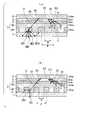
- the Otto type arrangement structureis shown separately. It is a cross-sectional schematic diagram of the organic EL element provided with the 2nd electrode side structure which has Otto type
- one of the first electrode and the second electrodeis an anode and the other is a cathode.
- the first electrodeis an anode and the second electrode is a cathode will be described as an example.
- the organic EL element of this inventionmay be provided with the layer which is not described below in the range which does not impair the effect of this invention.
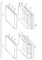
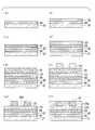
- FIG. 1is a schematic cross-sectional view for explaining an example of the organic EL element according to the first embodiment of the present invention.
- An organic EL element 10 shown in FIGS. 1A and 1Bincludes an anode (first electrode) 2, an organic layer 3 including a light emitting layer, and a cathode (second electrode) 4 in this order. 10.
- the low refractive index layer 5 and the metal layer 6are provided in this order on the opposite side of the cathode 4 from the organic layer 3.
- the cathode 4is made of a transparent conductive material, and the refractive index of the low refractive index layer 5 is lower than the refractive index of the organic layer 3.
- the anode 2is made of a transparent conductive material.
- FIG. 1Ashows an organic EL element in which the refractive index of the anode 2 is higher than that of the organic layer 3.
- FIG. 1Bshows an organic EL element in which the refractive index of the anode 2 is lower than the refractive index of the organic layer 3.
- the anode 2includes a plurality of anode hole portions 2A (see FIG. 9 (e)).
- the anode hole portion 2Amay be a hole that completely penetrates the anode or a non-through hole that does not completely penetrate the anode.
- the organic layer 3includes an anode hole inner surface covering portion 3a that covers the inner surface 2a of the anode hole 2A, and a layered portion 3b disposed between the anode 2 or the anode hole inner surface covering portion 3a and the cathode 4. .
- the bottom emission structureis when the substrate 1 is disposed on the anode 2 side.
- a case where the substrate 1 is disposed on the metal layer 6 sideis a top emission structure.
- a bottom emission structure in which the substrate 1 is present on the anode 2 sidewill be described as an example.
- the low refractive index layer 5 made of a material having a refractive index lower than that of the organic layer 3may include an air layer.
- the anode hole inner side surface covering portion 3 amay be constituted by a part of the layers constituting the organic layer 3.
- the refractive index of the organic layer 3means the average refractive index of all the layers including the light emitting layer.
- the period (pitch) at which adjacent anode hole portions 2A are arrangedis equal to or greater than the effective wavelength of the emitted light
- the shape of anode hole portion 2Ahas an effect of refracting light toward the substrate at the inner surface thereof.
- the refractive index of the anode 2is higher than the refractive index of the organic layer 3 as shown in FIG.
- the substrate 2is directed toward the substrate 1 side.
- a tapered shape that tapersis preferred.
- the shape of the anode hole portion 2Ais preferably a tapered shape that tapers toward the cathode 4 side.
- the anode hole portion 2Aregardless of the refractive index relationship between the anode 2 and the organic layer 3
- the shape of the taperis preferably tapered toward the substrate 1 side.
- the inner side surface of the anode hole portion 2Ais arranged perpendicular to the substrate surface, but such a configuration is not necessary.
- the acute angleis preferably 45 ° or more, more preferably 60 ° or more, and 75 °.
- the propagating light re-radiated from the SPP mode light and the guided mode light directed from the light emission position toward the anode sideare increased on the inner side surface 2a of the anode hole 2A.
- the lightis incident from the refractive index side, refracted toward the substrate side, and taken out from the outer surface of the substrate.
- the period (pitch) at which the adjacent anode hole 2A is arrangedis equal to or less than the effective wavelength of the emitted light, the shape of the anode hole 2A exhibits the effect of diffraction and the effect of the photonic crystal. If it is, it will not be specifically limited.
- the inner side surface 2a of the anode hole portion 2Ais perpendicular to the substrate surface regardless of the magnitude relationship between the refractive index of the inner side surface covering portion 3a and the refractive index of the anode 2. It is preferable to be close. This is because the photonic band gap is maximized when the inner side surface 2a of the anode hole 2A is perpendicular to the substrate surface. When the photonic band gap is increased, light cannot be present in a direction parallel to the substrate, so that light emitted from the organic layer 3 can be extracted from the outer surface of the substrate to the outside more efficiently.
- the bottom emission structurehas been described above as an example, the same applies to the top emission structure.
- FIG. 2is a schematic cross-sectional view for explaining an example of the organic EL element according to the second embodiment of the present invention.
- island-like organic layersinner surface covering portions 3a
- the island-shaped anodesare connected to each other and scattered therein.
- the organic EL element 20 shown in FIG. 2is an organic EL element 20 that includes an anode (first electrode) 12, an organic layer 13 including a light emitting layer, and a cathode (second electrode) 14 in this order.
- the low refractive index layer 15 and the metal layer 16are provided in this order on the opposite side of the cathode 14 from the organic layer 13.
- the cathode 14is made of a transparent conductive material, and the refractive index of the low refractive index layer 15 is lower than the refractive index of the organic layer 13.
- the anode 12is made of a transparent conductive material, and the refractive index of the anode 12 may be higher or lower than the refractive index of the organic layer 13.
- the anode 12includes a layered portion 12B and a plurality of anode convex portions 12A formed on and in contact with the layered portion 12B and arranged in an island shape in plan view.
- the organic layer 13has an anode convex side surface covering portion 13a that covers the outer surface 12a of the anode convex portion 12A, and a layered portion 13b that is disposed between the anode 12 or the anode convex side surface covering portion 13a and the cathode 14. .
- the low refractive index layer 15made of a material having a refractive index lower than that of the organic layer 13 may include an air layer.
- the bottom emission structureis when the substrate 11 is disposed on the anode 12 side
- the top emission structureis when the substrate 11 is disposed on the metal layer 16 side.
- a bottom emission structure in which the substrate 11 is present on the anode 12 sidewill be described as an example.
- the anode convex side surface covering portion 13 amay be constituted by a part of the layers constituting the organic layer 13.
- the refractive index of the organic layer 13refers to the average refractive index of all the layers including the light emitting layer.
- the refractive index of the anode 12is higher than the refractive index of the organic layer 13, a tapered shape that tapers toward the cathode 14 is preferable from the viewpoint of refracting the guided mode light more vertically.
- the refractive index of the anode 12is lower than the refractive index of the organic layer 13, a tapered shape that tapers toward the substrate 11 side is preferable.
- the outer side surface of the anode convex portion 12 ⁇ / b> Ais arranged perpendicular to the substrate surface, but it is not necessary to have such a configuration.
- the acute angleis preferably 45 ° or more, more preferably 60 ° or more, and 75 ° or more. Is even more preferable.
- the shape of the anode convex portions 12Aexhibits a diffraction effect or an effect of a photonic crystal. If it is, it will not be specifically limited.
- the outer surface 12a of the anode convex portion 12Ais in relation to the substrate surface regardless of the magnitude relationship between the refractive index of the anode convex portion side surface covering portion 13a and the refractive index of the anode 12. It is preferable to be close to vertical.
- the photonic band gapis the largest when the outer surface 12a of the anode protrusion 12A is perpendicular to the substrate surface, so that light cannot exist more in the direction parallel to the substrate, and more efficient. This is because the light emitted from the organic layer 13 can be extracted from the outer surface of the substrate to the outside.
- the refractive index of the low refractive index layeris lower than the refractive index of the organic layer.
- n L , n C , and n Orefractive indexes of the low refractive index layer, the cathode, and the organic layer
- B patternn L ⁇ n O ⁇ n C
- n L ⁇There are three cases: n C ⁇ n O (hereinafter referred to as “C pattern”) and n C ⁇ n L ⁇ n O (hereinafter referred to as “D pattern”).
- C patternn C ⁇ n O
- D patternn C ⁇ n L ⁇ n O
- the structure of the metal layer / low refractive index layer / cathodeis an Otto type arrangement.
- the configuration of the metal layer / low refractive index layer / cathodeis an Otto type arrangement
- the configuration of metal layer / low refractive index layer + cathode / organic layeris also an Otto type arrangement.
- the configuration of the metal layer / low refractive index layer + cathode / organic layeris an Otto type arrangement.
- the most preferable B to D patternis the C pattern.
- the configuration of the metal layer / low refractive index layer / cathode (transparent conductive layer)is an Otto type arrangement, and the metal layer / low refractive index layer + cathode (transparent conductive layer) / organic layer Since the Otto configuration is also used in the configuration, re-radiation of SPP mode light is most likely to occur from the metal layer. Further, since the refractive index increases in the order of the low refractive index layer, the cathode (transparent conductive layer), and the organic layer, total reflection does not occur at each interface, and the re-radiated SPP mode light is extracted as it is to the substrate side.
- PEDOT: PSSpoly (3,4-ethylene) is used as the material of the cathode (transparent conductive layer) with respect to the organic layer (typical refractive index: 1.7 to 1.8).
- B patternis preferred.
- a material having a lower refractive index than the material of the organic layeris selected from SOG as the material of the low refractive index layer.
- the D patternis not an Otto type arrangement.
- itis an Otto type arrangement only in the configuration of metal layer / low refractive index layer + cathode (transparent conductive layer) / organic layer, SPP mode light is re-radiated from the metal layer. The re-radiation of SPP mode light is further reduced.
- PEDOT: PSSis selected as the cathode material for the organic layer (typical refractive index: 1.7 to 1.8), and SOG is used as the material for the low refractive index layer. Therefore, there is a case where a material whose refractive index is an intermediate value between the cathode and the organic layer is selected.
- n O ⁇ n C ⁇ n L(hereinafter referred to as “E pattern”) and in the case of n C ⁇ n O ⁇ n L (hereinafter also referred to as “F pattern”), the Otto type arrangement is not achieved.
- the metal layer / low refractive index layer / cathodeis in an Otto type arrangement. Therefore, re-radiation of SPP mode light occurs from the metal layer, but the refractive index of the organic layer is lower than that of the low refractive index layer, so that the SPP mode light re-radiated at the cathode (transparent conductive layer) / organic layer interface. Most of the light is totally reflected and it is difficult to extract the light extracted as the propagation light on the anode side.
- the organic EL element of the present inventioncan be applied to both a top emission type and a bottom emission type organic EL element as described above.
- the substrateis a translucent substrate and usually needs to be transparent to visible light.
- transparent to visible lightmeans that it is only necessary to transmit visible light having a wavelength emitted from the light emitting layer, and it is not necessary to be transparent over the entire visible light region.
- a smooth substrate having a transmittance in visible light of 400 to 700 nm of 50% or moreis preferable.
- Specific examples of the substrateinclude a glass plate and a polymer plate.
- the glass plate materialexamples include soda lime glass, barium / strontium-containing glass, lead glass, aluminosilicate glass, borosilicate glass, barium borosilicate glass, and quartz.
- the material for the polymer plateexamples include polycarbonate, polymethyl methacrylate, polyethylene terephthalate, polyethylene naphthalate, polyether sulfide, and polysulfone.
- the transmittanceis preferably 50% or more and more preferably 70% or more with respect to the wavelength at which light emission has the maximum intensity.
- an opaque substratecan be used in addition to the same as described above.
- the thickness of the substrateis not limited depending on the required mechanical strength, but is preferably 0.01 mm to 10 mm, more preferably 0.05 mm to 2 mm.
- the interface which produces the said refractive effect in the organic EL element which concerns on 1st Embodimentbears the inner surface 2a (The interface of the anode 2 and the anode hole inner surface coating
- the interface causing the refraction effectis borne by the outer surface 12a of the anode convex portion 12A (the interface between the anode 12 and the anode convex portion side surface covering portion 13a of the organic layer 13).
- the refraction effectis caused by the interface between the anode and the anode side surface covering portion of the organic layer.
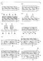
- FIG. 3is a schematic perspective view of the first embodiment and the second embodiment. As shown in FIG. 3, the anode hole portion of the first embodiment and the anode convex portion of the second embodiment are shown. In the case where the size of the anode hole portion and the anode convex portion are the same and the period (pitch) in which they are arranged is the same, the existence ratio of the interface does not change, so the same refraction effect is obtained. Have. Therefore, in the following description, it demonstrates taking the case of FIG. 1 (a), (b) which has an anode hole part.
- the anode 2is an electrode for applying a voltage between the anode 4 and injecting holes into the organic layer 3 from the anode 2, and is made of a metal, an alloy, a conductive compound, or a mixture thereof having a high work function. It is preferable to use a material. It is preferable to use a material having a work function of 4 eV or more and 6 eV or less so that the difference from the HOMO (High Occupied Molecular Orbital) level of the organic layer 3 does not become excessive.
- the material of the anode 2is not particularly limited as long as it is a translucent and conductive material.
- transparent materialssuch as indium tin oxide alloy (ITO), zinc oxide tin alloy (IZO), tin oxide, and zinc oxide are available.
- Conductive polymerssuch as inorganic oxides (PEDOT: PSS), polyaniline and conductive polymers doped with any acceptor, conductive light-transmitting materials such as carbon nanotubes, thin film metals, metal nanowires formed into thin films And composite materials containing these.
- the anode 2can be formed on the substrate 1 by, for example, a sputtering method, a vacuum deposition method, a coating method, a CVD method, an ion plating method, or the like.
- the thickness of the anode 2is not limited, but is, for example, 10 to 2000 nm, and preferably 50 to 1000 nm. If the thickness is less than 10 nm, it is difficult to increase the volume of the anode hole 2A, and the sheet resistance of the anode 2 is increased. If the thickness is more than 2000 nm, the flatness of the organic layer 3 cannot be maintained and the transmittance of the anode 2 is decreased. Because. When it is set as the structure which arrange
- the SPP mode light extracted at a predetermined angle into the organic layer 3 by the cathode structure of the Otto type arrangementis diffracted by the diffraction grating formed by the anode hole portion 2A and the organic layer 3, and the diffracted light is A period (pitch) that satisfies Equation (12) is selected so that total reflection is not performed at the substrate / air interface.
- the cathode 4is an electrode for injecting electrons into the light emitting layer, and it is preferable to use a material made of a metal, an alloy, a conductive compound, or a mixture thereof having a small work function. It is preferable to use a material having a work function of 1.9 eV or more and 5 eV or less so that the difference from the LUMO (Lower Unoccupied Molecular Orbital) level of the organic layer 3 does not become excessive.
- the material of the cathode 4needs to be a light-transmitting conductive material (non-metallic material) in order to form a cathode-side structure with an Otto type arrangement. Therefore, a nonmetallic material can be used among what was mentioned as said anode material.
- the thickness of the cathode 4is not limited, but is, for example, 30 nm to 1 ⁇ m, preferably 50 to 500 nm. If the thickness is less than 30 nm, the sheet resistance increases and the drive voltage increases. If it is thicker than 1 ⁇ m, heat and radiation damage during film formation and mechanical damage due to film stress accumulate in the electrode and organic layer.
- the organic layer 3has an inner surface covering portion 3a of the anode hole 2A and a layered portion 3b disposed between the anode 2 and the cathode 4.
- the organic layer 3may include a hole injection layer, a hole transport layer, an electron injection layer, an electron transport layer, and the like.
- the hole injection layeris a layer that assists the injection of holes into the light emitting layer
- the hole transport layeris a layer that transports holes to the light emitting region, and has a high hole mobility and usually has an ionization energy of 5.5 eV. The following is small.
- a hole injection layer and a hole transport layera material that injects and transports holes to the light emitting layer with a lower electric field strength is preferable.
- the electron injection layeris a layer that assists the injection of electrons into the light emitting layer
- the electron transport layeris a layer that transports electrons to the light emitting region, and a material having a high electron mobility is used.
- a material that injects and transports electrons to the light emitting layer with lower electric field strengthis preferable.
- the material for forming thisis not particularly limited as long as it can perform the above functions, and any material can be selected and used from known materials.
- the organic layer 3may be formed by a dry process such as an evaporation method or a transfer method, or may be formed by a wet process such as a spin coating method, a spray coating method, a die coating method, or a gravure printing method.
- the thickness of the layered portion 3b of the organic layer 3is not particularly limited. For example, it is 50 to 2000 nm, preferably 100 to 1000 nm. If it is thinner than 50 nm, extinction other than SPP coupling occurs, such as a decrease in internal QE due to punch-through current and lossy surface wave mode coupling due to metal layer 6, and if it is thicker than 2000 nm, the driving voltage Rises.
- the low refractive index layer 5is provided on the opposite side of the cathode 4 from the organic layer 3, and is preferably made of a transparent material having a lower refractive index than the translucent conductive material constituting the cathode 4.
- the material for the low refractive index layer 5is not particularly limited as long as it is a material having a lower refractive index than the translucent conductive material constituting the cathode 4.
- metal fluoridessuch as spin-on-glass (SOG) and magnesium fluoride (MgF 2 (typical refractive index: 1.38)) satisfying this refractive index condition, polytetrafluoroethylene (PTFE (typical refractive index) : 1.35)) and the like, silicon dioxide (SiO 2 (typical refractive index: 1.45)), various low-melting glasses, and porous materials.
- the low refractive index layer 5is composed of a layer including an air layer, and may have a refractive index lower than that of the translucent conductive material constituting the cathode 4.
- the metal layer 6is provided on the opposite side of the cathode 4 from the organic layer 3 via a low refractive index layer 5.
- any material or plasmon resonancecan be used as long as plasmon resonance is generated by the light emitted from the light emitting layer.
- a material having a negative real part of the complex dielectric constant and a large absolute valueis preferable. Examples of such materials include simple substances such as gold, silver, copper, zinc, aluminum, and magnesium, alloys of gold and silver, alloys of silver and copper, and alloys such as brass.
- the metal layer 6may have a laminated structure of two or more layers.
- the thickness of the metal layer 6is not limited. For example, it is 20 to 2000 nm, preferably 50 to 500 nm.
- the thicknessis less than 20 nm, the reflectance decreases and the front luminance decreases, and if the thickness is greater than 500 nm, heat, radiation damage, and mechanical damage due to film stress during film formation accumulate in the electrode and the organic layer.
- the effect of the second electrode side structure by the Otto type arrangement of the organic EL element of the present inventionwill be described below. Since the following is the principle content based on the calculation formula, it is described as the first electrode side structure and the second electrode side structure (in the present invention, one of the first electrode and the second electrode is an anode and the other is a cathode). is there).
- the angular frequency of surface plasmon polariton (SPP) generated on a flat metal surfaceis ⁇ sp and the real part of the in-plane component of the wave number is k sp
- SPPsurface plasmon polariton
- the dispersion line of the evanescent wave generated by the total reflection attenuation methodis given by the following equation (4).
- ⁇is high.
- an organic EL elementfor example, when a high refractive index layer / low refractive index layer / metal layer is provided adjacent to an organic layer, a predetermined incident angle (SPP dispersion curve) of light emitted from the organic light emitting layer is provided. And the light incident from the high refractive index layer to the high refractive index layer / low refractive index dielectric layer interface at an angle where the line and the dispersion line of the evanescent wave intersect each other) generate an evanescent wave. The evanescent wave excites SPP mode light on the metal surface.
- the SPP mode light excited on the metal surfacecan be extracted as propagating light radiated at a predetermined angle via the evanescent wave generated in the Otto type arrangement structure. That is, by introducing an Otto type arrangement structure in the organic EL element, it is possible to extract SPP mode light as propagating light emitted at a predetermined angle.
- the excitation / extraction of the SPP mode light via the evanescent waveoccurs when the low refractive index layer is a sufficiently thin film of about 20 to 300 nm. This is because if the low refractive index layer is too thick, the evanescent wave oozes from the organic layer does not reach the metal layer, and the evanescent wave and the SPP mode light cannot exchange energy.
- the metal layer and the high-refractive index layercome close to each other and the wave number of the SPP mode becomes larger than the formula (2), and the dispersion curve does not intersect with the propagation curve (3) of the propagation light. .
- the light extracted from the SPPis radiated at a predetermined angle corresponding to the intersection of the SPP dispersion curve and the evanescent wave dispersion line.
- the first electrode side structureAs the first electrode side structure, the guided mode light is refracted to the transparent substrate side and the incident angle to the interface (the angle formed by the incident ray and the normal of the incident interface) is reduced. An interface with a refractive index close to vertical was introduced. More specifically, by providing a hole in the first electrode and covering the inner surface of the hole with an organic layer, the first electrode serves as an interface having a refractive index close to perpendicular to the transparent substrate surface. Introduce an interface with the organic layer.
- the first electrode and the organic layerserve as an interface having a refractive index close to perpendicular to the transparent substrate surface. You may introduce the interface.
- the first electrode side structuremay be a refractive index modulation structure having periodicity in the in-plane direction of the substrate or a non-periodic refractive index modulation structure having no periodicity.
- the organic layer having different refractive index and the first electrodeare periodically arranged two-dimensionally.
- a diffraction effect(the effect of directing light at a predetermined angle with respect to the substrate surface) by a transmission diffraction grating (hereinafter simply referred to as “diffraction grating”), and an effect by a photonic crystal (light of a specific direction and frequency) Waveguide mode light can be taken out to the substrate side.
- period of the refractive index modulation structure of the first electrode side structure(hereinafter sometimes simply referred to as “period”) is larger than the effective wavelength (wavelength / refractive index), refraction becomes the dominant mechanism, It is thought that it will be taken out.
- period of the refractive index modulation structure of the first electrodeis equal to or less than the effective wavelength, it is considered that light is extracted because the effect of the diffraction grating or the effect of the photonic crystal becomes the dominant mechanism. It is done.
- FIG. 4is a schematic cross-sectional view of an organic EL element having a second electrode side structure having an Otto type arrangement. First, the principle of extracting SPP mode light as guided mode light by this second electrode side structure will be described with reference to FIG. In FIG. 4, the first electrode side structure is omitted.
- n lowis the refractive index of the low refractive index layer
- n subis the refractive index of the substrate
- n OLEDis the average refractive index of the first electrode, the organic layer, and the second electrode
- ⁇ 1is the dielectric constant of the metal layer.
- k spis the in-plane direction component of the wave number vector of the SPP mode light
- k 0is the wave number (2 ⁇ / ⁇ ) of light in vacuum ( ⁇ is the wavelength of light emitted from the light emitting layer)
- ⁇is high
- the wave number k sp of the SPP mode lightis approximately given by the following equation (5) from the equation (2).
- FIG. 5is a partial schematic cross-sectional view including the first electrode side structure of the organic EL element including the first electrode side structure including the transmission diffraction grating. It is assumed that light extracted at a predetermined angle ⁇ is diffracted by a diffraction grating having a period (pitch) p.
- the condition for diffracting to the substrate side at a predetermined angle ⁇ sub with respect to the substrate surfaceis that the difference between the in-plane wave number of incident light incident on the diffraction grating and the in-plane wave number of diffracted light is an integral multiple of 2 ⁇ / p.
- Equation (9)is obtained from Equation (7) and Equation (8). The condition under which total reflection does not occur at the interface between the substrate and air is to satisfy equation (10).
- the expression (11)approximately satisfies the following expression (12).
- the peak wavelength of the emission spectrum of the light emitting layeris adopted as ⁇ in the formula (12). As the peak wavelength, the peak wavelength of the photoluminescence spectrum can be used.
- the above theoretical analysisis a one-dimensional analysis.
- a one-dimensional diffraction grating structurea diffraction grating structure in which refractive index modulation structures are arranged at regular intervals in a predetermined direction on the substrate surface
- a diffraction effect based on the analysisis obtained. Since the one-dimensional diffraction grating structure does not have a refractive index modulation structure in a direction orthogonal to the one direction, a diffraction effect does not occur for light in the orthogonal direction (light component).
- the two-dimensional diffraction grating structurehas a refractive index modulation structure in the orthogonal direction, and a diffraction effect is added also in that direction.
- the diffraction effectis larger in the two-dimensional diffraction grating structure than in the one-dimensional diffraction grating structure. Therefore, in an organic EL element having a configuration that satisfies the condition of Expression (12) in a predetermined cross section, the light extraction efficiency can be improved regardless of whether the configuration is a one-dimensional diffraction grating structure or a two-dimensional diffraction grating structure. .
- a photonic crystalis a structure having periodically different refractive indexes.
- the first electrode side structureis regarded as a two-dimensional photonic crystal.
- Can doIn the two-dimensional photonic crystal, a photonic band gap is formed with respect to the two-dimensional in-plane direction, and thus light having a wavelength within the photonic band gap cannot exist in the two-dimensional in-plane direction.
- no photonic band gapis formed, so that light can be emitted. With this mechanism, light that cannot travel in the in-plane direction is redistributed in the vertical direction, so that light can be efficiently extracted to the transparent substrate side.
- the first electrode side structureis a non-periodic structure having no periodicity in the in-plane direction of the substrate, the incident angle of the light incident on the first electrode structure is diffracted at a random position and phase and strengthened. Is not biased to a specific angle. Therefore, by having such a structure on the first electrode side, relatively uniform (highly diffusible) orientation characteristics can be obtained. That is, when the first electrode side structure is a periodic structure, an alignment characteristic in which the light intensity at a specific radiation angle is increased by the effect of strengthening the emitted light by the diffraction grating, whereas the first electrode side structure can be obtained. When the one-electrode structure is a non-periodic structure, relatively uniform alignment characteristics can be obtained. Therefore, the first electrode side structure can be selected to be a structure having periodicity or a non-periodic structure according to a required light distribution characteristic.
- one of the first electrode and the second electrodeis an anode and the other is a cathode.
- a configuration in which the first electrode is an anode and the second electrode is a cathodewill be described as an example.
- the light propagation method indicated by the arrows in FIGS. 1A and 1Bis schematically shown in order to easily understand the principle of the effect of refraction.
- the operation and effect when the refractive index of the anode 2 is higher than the refractive index of the organic layer 3will be described with reference to FIG.
- FIG. 1Aamong the light emitted at the point Ai of the light emitting layer included in the organic layer 3, the light traveling to the cathode 4 side is larger than the critical angle at the interface between the cathode 4 and the low refractive index layer 5.
- an evanescent wave(arrow A2) is generated in the low refractive index layer 5.
- a light emission point (or light emission location) Aiindicates a light emission point at a position overlapping the anode hole 2A in plan view (hereinafter, light emission at this point is referred to as “in light emission”).
- the light emission point Aoindicates a light emission point at a position overlapping the anode 2 in plan view (hereinafter, light emission at this point may be referred to as “out light emission”).
- the light emission point Aeindicates light emission at the boundary between “in light emission” and “out light emission” (hereinafter, light emission at this point may be referred to as “in-out edge light emission”).
- in-out edge light emissionFor “out emission” and “in-out edge emission”, the arrow indicating total reflection at the interface between the cathode 4 and the low refractive index layer 5 is omitted.
- this function and effectonly the case of “in light emission” is described in detail.
- the light extracted from the cathode side structure (cathode 4, low refractive index layer 5, metal layer 6) to point B of the organic layer 3propagates like B1 and is extracted to the substrate 1. That is, the light B1 traveling through the organic layer 3 from the point B is incident on the anode 2 from the upper surface of the anode 2, and then the substrate 1 at the interface between the organic layer 3 and the anode 2 (inner side surface 2a of the anode hole portion 2A). After being refracted to the side and proceeding through the organic layer 3 and refracting at the interface between the organic layer 3 and the substrate 1, it can be taken out through the substrate 1.
- the angle of incidence on the substrate 1is small due to refraction at the interface between the organic layer 3 and the anode 2 (inner side surface 2a of the anode hole 2A) (substrate (Direction closer to the normal of 1).
- Total reflectionoccurs at the interface between the anode 2 and the substrate (for example, glass) 1 and at the interface between the substrate 1 and the outside (air) at an angle greater than the critical angle, but the inner surface 2a ( Since the incident angle to the substrate 1 is changed to a small angle by refraction at the interface between the anode 2 and the organic layer 3 extending perpendicularly to the substrate 11, the light that can avoid the total reflection is increased and the light extraction efficiency is increased. improves. That is, the light extraction efficiency is improved by having the configuration including the inner side surface 2a of the anode hole portion 2A (the interface between the anode 2 and the organic layer 3 extending perpendicularly to the substrate 1).
- the current densityis highest in the vicinity of the shortest distance between the cathode 4 and the anode 2, and the amount of light emission increases.
- the light emission at the Co point of the light emitting layer included in the organic layer 13schematically shows the light emission at the point where this light emission amount is large among the “out light emission”.
- the light C ⁇ b> 1is light traveling toward the substrate side in a direction perpendicular to the substrate, and is refracted at the interface with the substrate 1. It advances and is taken out outside.
- the light C2is incident on the anode 2 from the upper surface of the anode 2, and then refracted at the inner side surface 2a of the anode hole 2A (the interface between the anode 2 and the organic layer 3 extending perpendicularly to the substrate 1), After passing through the organic layer 3 and refracting at the interface between the organic layer 3 and the substrate 1, it can be taken out through the substrate 1.
- the angle of incidence on the substrate 1is small due to refraction at the interface between the organic layer 3 and the anode 2 (the inner surface 2a of the anode hole 2A) ( The direction closer to the normal of the substrate 1).
- the operation and effect when the refractive index of the anode 2 is lower than the refractive index of the organic layer 3will be described with reference to FIG.
- FIG. 1Bamong the light emitted at the point Ai of the light emitting layer included in the organic layer 3, the light that has traveled to the cathode 4 side is the anode until it is extracted to the point B of the organic layer 3. Since the refractive index of 2 is higher than the refractive index of the organic layer 3 (in the case of FIG. 1A), the description thereof is omitted.
- the light B1 traveling through the organic layer 3 from the point Bis refracted toward the substrate 1 at the interface between the organic layer 3 and the anode 2 (inner side surface 2a of the anode hole 2A) and travels through the anode 2, and the organic layer 3 After being refracted at the interface between the substrate 1 and the substrate 1, it can be taken out through the substrate 1.
- the angle of incidence on the substrate 1is small due to refraction at the interface between the organic layer 3 and the anode 2 (inner side surface 2a of the anode hole 2A) (substrate (Direction closer to the normal of 1).
- Total reflectionoccurs at the interface between the anode 2 and the substrate (for example, glass) 1 and at the interface between the substrate 1 and the outside (air) at an angle greater than the critical angle, but the inner surface 2a ( Since the incident angle to the substrate 1 is changed to a small angle by refraction at the interface between the anode 2 and the organic layer 3 extending perpendicularly to the substrate 11, the light that can avoid the total reflection is increased and the light extraction efficiency is increased. improves. That is, the light extraction efficiency is improved by having the configuration including the inner side surface 2a of the anode hole portion 2A (the interface between the anode 2 and the organic layer 3 extending perpendicularly to the substrate 1).
- the vicinity of the shortest distance between the cathode 4 and the anode 2has the highest current density and the amount of light emission increases.
- the light emission at the Co point of the light emitting layer included in the organic layer 13schematically shows the light emission at the point where this light emission amount is large among the “out light emission”.
- the light C ⁇ b> 1is light traveling toward the substrate side in a direction perpendicular to the substrate, and is refracted at the interface with the substrate 1. It advances and is taken out outside.
- the light C2is refracted at the inner surface 2a of the anode hole 2A (the interface between the anode 2 and the organic layer 3 extending perpendicularly to the substrate 1) and refracted at the interface between the organic layer 3 and the substrate 1. Thereafter, it can be taken out through the substrate 1.
- the angle of incidence on the substrate 1is small due to refraction at the interface between the organic layer 3 and the anode 2 (the inner surface 2a of the anode hole 2A) ( The direction closer to the normal of the substrate 1).
- the organic EL element 10 of the first embodiment of the present inventionwhen the anode holes are periodically arranged, the anode 2 and the organic layer 3a covering the anode hole inner side surface 2a form a diffraction grating.
- the effects of the diffraction gratingwill be schematically described with reference to FIG.
- the way of light propagation indicated by arrows in FIG. 6Ais schematically shown in order to easily understand the principle of the effect of the diffraction grating.
- the light traveling toward the cathode 4is incident at the interface between the cathode 4 and the low refractive index layer 5 at a large incident angle greater than the critical angle (arrow B1)
- an evanescent wave(arrow B2) is generated in the low refractive index layer 5.
- the generated evanescent waveoozes out to the interface between the metal layer 6 and the low refractive index layer 5, and the surface plasmon polariton SPP (arrow B3) is excited.
- the excited SPPis radiated to the cathode 4 at a predetermined angle (arrow B5) through resonance with the evanescent wave (arrow B4), and can be extracted to the organic layer 3 as propagating light.
- the light extracted from the cathode side structure (cathode 4, low refractive index layer 5, metal layer 6) to point Bpropagates through the organic layer and enters the diffraction grating.
- the incident lightis diffracted by the diffraction grating in a predetermined direction (a direction satisfying the Nth order strengthening condition).
- the diffracted lightis emitted at a certain predetermined angle because the diffracted light at each diffraction point is emitted while interfering with each other.
- the arrows BD1 and BD2light incident on the interface between the substrate (for example, glass) and the outside (for example, air) at a critical angle or less is directly extracted to the outside.
- arrow BD1 and the arrow BD2are stronger than other propagation directions due to interference as described above, it is possible to extract light having high intensity at a specific angle, and light extraction efficiency is improved.
- an arrow BD3rlight that is incident on the interface between the substrate and the outside at an incident angle greater than the critical angle is totally reflected (arrow BD3r) to become substrate mode light and cannot be extracted outside the substrate.
- light incident on the interface between the organic layer or the anode and the substrate at an incident angle greater than the critical angleis totally reflected to be guided mode light, and similarly cannot be extracted outside the substrate.
- the anode layeris periodically arranged with a period equal to or less than the emission wavelength, thereby covering the anode 2 and the inner surface 2a of the anode hole.
- the photonic crystal 3aforms a photonic crystal
- the function and effect of the photonic crystalwill be schematically described with reference to FIG.
- the way of propagation of light indicated by arrows in FIG. 6Bis schematically shown in order to easily understand the principle of the effect of the photonic crystal.
- the light traveling to the cathode 4 sideis incident at the interface between the cathode 4 and the low refractive index layer 5 at a large incident angle greater than the critical angle (arrow C1)
- an evanescent wave(arrow C2) is generated in the low refractive index layer 5.
- the generated evanescent waveoozes out to the interface between the metal layer 6 and the low refractive index layer 5, and the surface plasmon polariton SPP (arrow C3) is excited.
- the excited SPPis radiated to the cathode 4 at a predetermined angle (arrow C5) through resonance with the evanescent wave (arrow C4), and can be extracted to the organic layer 3 as guided mode light.
- the light extracted from the cathode side structure (cathode 4, low refractive index layer 5, metal layer 6) to point Cpropagates through the organic layer and enters the photonic crystal structure.
- a structure equal to or smaller than the wavelength of lightexists in the two-dimensional direction, a photonic band gap is formed in the two-dimensional direction, and light in the band gap frequency region cannot propagate in the two-dimensional direction (two-dimensional direction). Light confinement effect).
- the periodic structureis formed by the anode 2 and the organic layer 3a covering the inner surface of the anode hole portion 2a, the propagation of light is restricted in the direction of the arrow CD2 parallel to the substrate. It is.
- the propagation of lightis not limited.
- propagating light in the organic layertravels in a direction in which the light is nearly perpendicular to the substrate. Since the direction of the arrow CD1 is nearly perpendicular to the substrate, light can be extracted efficiently without being totally reflected even at the interface between the substrate and air.
- the organic EL element 20 of the second embodiment of the present inventionhas a reverse sea-island relationship in the plan view of the anode and the organic layer.
- the organic EL element 20 of the second embodimentis basically also used in the organic EL element 20 of the second embodiment. 10 has the same optical effect. Therefore, detailed description of the operational effects of the second embodiment is omitted.
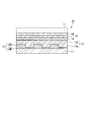
- FIG. 7is a diagram illustrating an example of an image display device including the organic EL element. Further, the organic EL element may have a bottom emission structure or a top emission structure, but the following description will be made with an example of a bottom emission structure.
- the image display device 100 shown in FIG. 7is a so-called passive matrix type image display device.
- the anode wiring 104In addition to the organic EL element 10, the anode wiring 104, the anode auxiliary wiring 106, the cathode wiring 108, the insulating film 110, and the cathode partition 112 are used. , A sealing plate 116 and a sealing material 118.
- a plurality of anode wirings 104are formed on the substrate 1 of the organic EL element 10.
- the anode wirings 104are arranged in parallel at a constant interval.
- the anode wiring 104is made of a transparent conductive film, and for example, ITO (Indium Tin Oxide) can be used.
- the thickness of the anode wiring 104can be set to 100 nm to 150 nm, for example.
- An anode auxiliary wiring 106is formed on the end of each anode wiring 104.
- the anode auxiliary wiring 106is electrically connected to the anode wiring 104.
- the anode auxiliary wiring 106functions as a terminal for connecting to the external wiring on the end portion side of the substrate 1, and the drive circuit (not shown) provided outside via the anode auxiliary wiring 106.
- a currentcan be supplied to the anode wiring 104.
- the anode auxiliary wiring 106is made of a metal film having a thickness of 500 nm to 600 nm, for example.
- a plurality of cathode wirings 108are provided on the organic EL element 10.
- the plurality of cathode wirings 108are arranged so as to be parallel to each other and orthogonal to the anode wiring 104.
- Al or an Al alloycan be used for the cathode wiring 108.
- the thickness of the cathode wiring 108is, for example, 100 nm to 150 nm.
- a cathode auxiliary wiring(not shown) is provided at the end of the cathode wiring 108 and is electrically connected to the cathode wiring 108. Therefore, a current can be supplied from the external drive circuit to the cathode wiring 108 via the cathode auxiliary wiring.
- an insulating film 110is formed on the substrate 1 so as to cover the anode wiring 104.
- a rectangular opening 120is provided in the insulating film 110 so as to expose a part of the anode wiring 104.
- the plurality of openings 120are arranged in a matrix on the anode wiring 104.
- the organic EL element 10is provided between the anode wiring 104 and the cathode wiring 108. That is, each opening 120 becomes a pixel. Accordingly, a display area is formed corresponding to the opening 120.
- the thickness of the insulating film 110can be set to, for example, 200 nm to 10,000 nm, and the size of the opening 120 can be set to, for example, 100 ⁇ m ⁇ 100 ⁇ m.
- the organic EL element 10is located between the anode wiring 104 and the cathode wiring 108 in the opening 120. In this case, the anode 2 of the organic EL element 10 is in contact with the anode wiring 104 and the cathode 4 is in contact with the cathode wiring 108.
- the thickness of the organic EL element 10can be set to, for example, 150 nm to 200 nm.
- a plurality of cathode partition walls 112are formed on the insulating film 110 along a direction orthogonal to the anode wiring 104 in plan view.
- the cathode partition 112plays a role for spatially separating the plurality of cathode wirings 108 so that the wirings of the cathode wirings 108 do not conduct with each other. Accordingly, the cathode wiring 108 is disposed between the adjacent cathode partition walls 112.
- the size of the cathode partition 112for example, the one having a height of 2 ⁇ m to 3 ⁇ m and a width of 10 ⁇ m can be used. *
- the substrate 1is bonded to each other through a sealing plate 116 and a sealing material 118.
- the space in which the organic EL element 10 is providedcan be sealed, and the organic EL element 10 can be prevented from being deteriorated by moisture in the atmosphere.
- the sealing plate 116for example, a glass substrate having a thickness of 0.7 mm to 1.1 mm can be used.
- the sealing plate 116may not be transparent when light is extracted from the substrate 1 side as in the case of a bottom emission type element.
- the sealing plate 116needs to be transparent to at least a part of the light emission wavelength region.
- a currentcan be supplied to the organic EL element 10 via the anode auxiliary wiring 106 and the cathode auxiliary wiring (not shown) by a driving device (not shown) to cause the light emitting layer to emit light. Then, light can be emitted from the substrate 1 through the substrate 1.
- An imagecan be displayed on the image display device 100 by controlling the light emission and non-light emission of the organic EL element 10 corresponding to the above-described pixel by the control device.
- FIG. 8is a diagram illustrating an example of an illumination device including the organic EL element 10 described above.
- the lighting device 200 shown in FIG. 8is installed adjacent to the organic EL element 10 and the substrate 1 (see FIG. 1) of the organic EL element 10, and is connected to the anode 2 (see FIG. 1).
- the lighting circuit 201has a DC power source (not shown) and a control circuit (not shown) inside, and supplies a current between the anode 2 and the cathode 4 of the organic EL element 10 through the terminal 202 and the terminal 203. Then, the organic EL element 10 is driven, the light emitting layer is caused to emit light, light is emitted from the substrate 1, and used as illumination light.
- the light emitting layermay be made of a light emitting material that emits white light, and each of the organic EL elements 10 using light emitting materials that emit green light (G), blue light (B), and red light (R). A plurality of them may be provided so that the combined light is white.
- the manufacturing method of the organic EL element 10will be described with reference to FIG.
- the organic EL element 10 of the first embodiment and the organic EL element 20 of the second embodimentare different from each other only in that the sea-island relationship between the anode 2 and the organic layer 3 is opposite to each other.
- the manufacturing method of the organic EL element 10will be mainly described.
- the anode 2is formed on the substrate 1.
- the formation of the anode 2is not limited.
- a wet processsuch as a coating method can be used.
- the surface treatmentincludes high-frequency plasma treatment, sputtering treatment, corona treatment, UV ozone irradiation treatment, ultraviolet irradiation treatment, oxygen plasma treatment, and the like.
- anode buffer layer(not shown) instead of or in addition to the surface treatment of the surface treatment of the anode 2.
- a spin coating method, a casting method, a micro gravure coating method, a gravure coating method, a bar coating method, a roll coating method, a wire bar coating method, a dip coating method, a spray A filmcan be formed using a coating method, a screen printing method, a flexographic printing method, an offset printing method, an application method such as an inkjet printing method, an immersion method, an electrochemical method, or the like.
- the anode buffer layerwhen the anode buffer layer is produced by a dry process, the anode buffer layer can be formed by using the plasma treatment exemplified in Japanese Patent Application Laid-Open No. 2006-30312.
- a method of forming a film of a single metal, a metal oxide, a metal nitride, or the likecan be mentioned.
- Specific film forming methodsinclude an electron beam evaporation method, a sputtering method, a chemical reaction method, a coating method, and a vacuum evaporation method. The method etc. can be used.
- a method using photolithographycan be used to form the anode hole 2A.
- a positive resist solutionis applied on the anode 2 and the excess resist solution is removed by spin coating or the like, thereby forming a resist layer 9.
- FIG. 9Dwhen a mask (not shown) on which a predetermined pattern for forming the anode hole 2A is drawn is applied and exposure is performed with ultraviolet rays (UV), electron beams (EB), etc., FIG. As shown, the resist layer 9 is exposed to a predetermined pattern corresponding to the anode hole 2A. Then, the resist layer 9a in the exposed pattern portion is removed using a developer. Thus, the surface of the anode 2 is exposed corresponding to the exposed pattern portion (FIG. 9D).
- UVultraviolet rays
- EBelectron beams
- the exposed portion of the anode 2is removed by etching to form an anode hole portion 2A.
- etchingeither dry etching or wet etching can be used.
- the shape of the anode hole portion 2Acan be controlled by combining isotropic etching and anisotropic etching.
- dry etchingreactive ion etching (RIE) or inductively coupled plasma etching can be used.
- RIEreactive ion etching
- wet etchinga method of immersing in dilute hydrochloric acid, dilute sulfuric acid, or aqueous iron chloride can be used. By this etching, the surface of the substrate 1 is exposed corresponding to the pattern.
- the organic layer 3is filled into the anode hole 2A to form the anode hole inner side surface covering part 3a.
- the inner side surface 2a of the anode hole 2Aonly needs to be covered with the organic layer 3, even if the anode hole 2A is not completely filled with the organic layer 3, only a part of the anode hole 2A is filled and the anode hole 2A is filled.
- a configuration in which the inner side surface 2a of 2A is coveredmay be employed.
- the formation of the anode hole inner side surface covering portion 3ais not limited in the same manner as the formation of the anode 2, but a conventionally known method can be used.
- anode hole inner side surface covering portion 3acovers the inner side surface 2a of the anode hole portion 2A, the formation conditions are adjusted depending on whether the anode hole portion 2A is completely filled or partially filled.
- the anode hole portion 2Acan also be formed by direct processing by laser light irradiation.
- the workpieceis directly drilled with a laser beam, or the workpiece is irradiated with an interference pattern of laser light to perform uneven processing. Therefore, since the mask is not formed with a photoresist, the number of processing steps is reduced.
- the laser used for processinginclude a pulse carbon dioxide laser, a Q switch Nd: YAG laser and its harmonics, a titanium sapphire laser, and an excimer laser.
- a surface protective filmmay be used to prevent damage to the anode 2 due to laser irradiation.
- the stepmay be the same as the step of forming the hole 2A.
- the anode etchingis performed so that the plurality of anode protrusions 12A are not isolated from each other. Is not performed until the substrate is exposed, and must be stopped halfway. This is for taking conduction between the anode protrusions.
- a cathode 4is formed on the organic layer 3.
- the formation of the cathode 4can be performed using the same method as the formation of the anode 2 and is not limited.
- a resistance heating vapor deposition methodan electron beam vapor deposition method, a sputtering method, an ion plating method, a CVD method, or the like can be used.
- a low refractive index layer 5is formed on the cathode 4.
- the formation of the low refractive index layer 5is not limited.
- a resistance heating vapor deposition method, an electron beam vapor deposition method, a sputtering method, an ion plating method, a CVD method, or the likecan be used.
- the low-refractive index layer 5is a low-refractive index layer including an air layer
- the SOG materialis left at a predetermined position in the SOG layer using photolithography.
- the low refractive index layeris formed by etching away the SOG layer so that the portion where the SOG layer is removed becomes an air layer.
- a metal layer 6is formed on the low refractive index layer 5.
- formation in particularis not limited in formation of the metal layer 6,
- a vapor deposition method and sputteringcan be used.
- the organic EL element 10can be manufactured by the above process. Moreover, after these series of processes, it is preferable to use the organic EL element 10 stably for a long period of time and to attach a protective layer and a protective cover (not shown) for protecting the organic EL element 10 from the outside.
- a protective layerpolymer compounds, metal oxides, metal fluorides, metal borides, silicon compounds such as silicon nitride and silicon oxide, or sacrificial layer (protective layer to be removed in the subsequent process) ionization tendency such as zinc A large metal or the like can be used. And these laminated bodies can also be used.
- the protective covera glass plate, a plastic plate whose surface has been subjected to low water permeability treatment, a metal, or the like can be used. It is preferable to adopt a method in which the protective cover is sealed by being bonded to the substrate 1 with a thermosetting resin, a photocurable resin, or frit glass. In this case, it is preferable to use a spacer because a predetermined space can be maintained and the organic EL element 10 can be prevented from being damaged. If an inert gas such as nitrogen, argon, or helium is sealed in this space, it becomes easy to prevent the upper metal layer 6 from being oxidized.
- an inert gassuch as nitrogen, argon, or helium
- the metal layer 26is formed on the substrate 21.
- the formation of the metal layer 26is not particularly limited. For example, vapor deposition or sputtering can be used.
- the low refractive index layer 25is formed on the metal layer 26.
- the formation of the low refractive index layer 25is not limited.
- a resistance heating vapor deposition method, an electron beam vapor deposition method, a sputtering method, an ion plating method, a CVD method, or the likecan be used.
- the low-refractive index layer 25is a low-refractive index layer including an air layer, for example, after the SOG layer is formed, the SOG material is left at a predetermined position using photolithography in the SOG layer.
- the low refractive index layeris formed by etching away the SOG layer so that the portion where the SOG layer is removed becomes an air layer.
- the cathode 24is formed on the low refractive index layer 25.
- the formation of the cathode 24is not limited.
- a resistance heating vapor deposition method, an electron beam vapor deposition method, a sputtering method, an ion plating method, a CVD method, or the likecan be used.
- an organic layer layer portion 23 bis formed on the cathode 24.
- a conventionally known methodcan be used.
- a methodsuch as a vacuum deposition method, a spin coating method, a casting method, or an LB method can be used.
- the anode 22is formed on the layered portion 23b of the organic layer.
- the formation of the anode 22is not limited like the cathode 24.
- a resistance heating vapor deposition method, an electron beam vapor deposition method, a sputtering method, an ion plating method, a CVD method, or the likecan be used.
- a resist pattern 27 having a predetermined patternis formed on the anode 22 as shown in (f), and the anode is etched as shown in (g) using this resist pattern as a mask to form the opening 22A.
- the resist 27is removed.
- As an etching methodthe same etching method as that used in the etching of the anode 1 of Embodiment 1 can be used.
- the anode hole inner side surface covering portion 23ais formed so as to fill the opening 22A.
- a conventionally well-known methodcan be used for formation of the inner surface covering part 23a. For example, methods such as a vacuum deposition method, a spin coating method, a casting method, and an LB method can be used.
- an anode layeris further formed on the entire surface of the sea-island structure of the anode 22 and the organic layer 23.
- FIG. 11shows the effect of the organic EL element of the present invention using a finite difference time domain method (FDTD (Finite Difference Time Domain) Method), and the light extraction efficiency of the adjacent anode portion (anode hole portion or anode convex portion). Shows the result of computer simulation of the dependence on the period (pitch) at which the data is arranged.
- FDTDFinite Difference Time Domain
- Maxwell's equation describing the time change of the electromagnetic fieldis differentiated spatially and temporally, and the time change of the electromagnetic field at each point in the space is tracked. More specifically, the light emission in the light emitting layer is regarded as radiation from a minute dipole, and the time change of the radiation (electromagnetic field) is traced.
- the simulation resultshows the result of light extraction to the substrate.
- ⁇ on the horizontal axisis the wavelength in vacuum
- ⁇ on the vertical axisis the light extraction efficiency (ratio of the light intensity extracted from the substrate to the total radiation intensity from the dipole).
- the light extraction efficiencywas simulated using the FDTD method with the dipole as the light source being random (dipole moments are random in the x, y, and z directions). Results are shown.
- the X and Y directionsare directions parallel to the substrate surface
- the Z directionis a direction perpendicular to the substrate surface.
- FIG. 12is a cross-sectional view showing a model structure of a bottom emission type organic EL element used in the simulation.
- the refractive index values used for the calculationare as follows.
- the substrate 1is made of glass, and a refractive index of 1.52 is used.
- the anode 2is made of ITO
- the refractive indexis 1.82 + 0.009i at 550 nm, and other wavelengths are extrapolated by the Lorentz model.
- 1.72was used as the refractive index of the organic layer 3.
- the cathode 4is made of a-ITO (amorphous ITO), the refractive index is 1.82 + 0.009i at 550 nm, and other wavelengths are extrapolated by the Lorentz model.
- the low refractive index layer 5is made of a material containing spin-on-glass (SOG), and a refractive index of 1.25 is used. Further, assuming that the metal layer 6 is made of aluminum (Al), the refractive index is 0.649 + 4.32i at 550 nm, and other wavelengths are extrapolated by the Drude model.
- the layer thicknesses of the anode 2, the layered portion 3b of the organic layer 3, the cathode 4, the low refractive index layer 5, and the metal layer 6were 150 nm, 100 nm, 50 nm, 50 nm, and 100 nm, respectively.
- positionedwas calculated at 200 nm, 300 nm, 500 nm, 900 nm, 2000 nm, 4000 nm, and 8000 nm, respectively.
- the diameter D of the anode hole part 3a in each period (pitch)was set to 100 nm, 150 nm, 250 nm, 450 nm, 1000 nm, 2000 nm, and 4000 nm which are 1 ⁇ 2 of the period (pitch).
- the anode opening 2Ahas a translational structure in the depth direction of the drawing.
- the anode opening 2Ahas a line-like opening shape extending infinitely in the plane in plan view. This is because the light radiation pattern corresponding to the period (pitch) of the opening 2A is more clearly seen when the magnetic field strength distribution shape is calculated later.
- a structure having a cathode side structure with an Otto type arrangement, but having no first electrode side structure for extracting propagating light extracted into the organic layer to the outside without using guided mode lighthereinafter referred to as the structure
- a structure having only an Otto type arrangement), a cathode side structure having an Otto type arrangement, and a structure having no first electrode side structure for extracting propagating light to the outside instead of being guided mode lighthereinafter referred to as “Otto type arrangement”.
- the standard structuremeans a structure in which an anode layer, an organic layer, and a cathode metal layer are formed in this order on a glass substrate.
- the standard structurewas such that the substrate was made of glass, the anode was made of ITO, the organic layer was sandwiched, and the cathode was made of Al.
- Refractive indexes of 1.52, 1.82 + 0.009i, 1.72, and 0.649 + 4.32iwere used, respectively, and the anode, organic layer, and cathode layer thicknesses were 150 nm, 100 nm, and 100 nm, respectively. It was.
- the organic EL element of the present inventionhas a cycle (pitch) in which all the calculated anode portions are arranged, compared with the structure having only the Otto type arrangement or the standard structure at a wavelength of 680 nm or less. It can be confirmed that the light extraction efficiency is improved. In particular, it can be confirmed that the light extraction efficiency is increased at a wavelength of 680 nm or less at a period (pitch) of 500 nm to 2000 nm. Further, it can be confirmed that the light extraction efficiency is remarkably increased when the period (pitch) is in the range of 900 to 2000 nm. This result cannot be predicted based on the structure of the cathode side structure and the anode side structure of the Otto type arrangement, but has been revealed for the first time by the simulation of the present invention.
- FIG. 13 (a)shows the result of the FDTD method simulation of the intensity distribution of the electric field of the emitted light from the horizontal dipole in the case of the structure having only the Otto type arrangement.
- the wavelength of the emitted lightwas 480 nm.
- the intensity distributionis shown with the substrate on the top and the metal layer on the bottom.
- the white line crossing the electric field intensity distributionis the boundary line between adjacent layers.
- the distribution diagramcorresponds to the electric field intensity distribution in the substrate, the anode, the organic layer, the cathode, the low refractive index layer, the metal layer, and the air layer in order from the top.
- the light sourceis placed at the right end of the figure, and the electric field intensity distribution in the right half is omitted.
- 13B and 13Cshow the intensity distribution of the electric field of the emitted light from the horizontal dipole when the period (pitch) of the anode portion in the organic EL element of the embodiment of the present invention is 500 nm and 900 nm, respectively.
- the result obtained by the simulation of FDTD methodis shown.
- a white line running in the vertical direction in the anode layerrepresents the inner surface of the anode hole.
- the wavelength of the emitted lightwas 480 nm.
- the intensity distributionis shown with the substrate on the top and the metal layer on the bottom.
- each of FIGS. 13B and 13C using the organic EL element of the present inventionis organic from the dipole light source. After propagating through the layer in the left direction, light is emitted obliquely upward, and it can be confirmed that light emission in a specific direction is enhanced by the effect of the diffraction grating. As for the period (pitch) of the anode part, it can be confirmed that the period (pitch) of 900 nm in FIG. This is difficult to predict even for those skilled in the art, and can be known only after simulation.
- FIG. 14Ashows a result obtained by FDTD simulation of the intensity distribution of the magnetic field of the emitted light from the dipole in the vertical (z) direction in the case of the structure having only the Otto type arrangement.
- the wavelength of the emitted lightwas 480 nm.
- the intensity distributionis shown with the substrate on the top and the metal layer on the bottom.
- FIGS. 14B and 14Cshow the intensity distribution of the magnetic field of the emitted light from the horizontal dipole when the period (pitch) of the anode portion in the organic EL element of the embodiment is 500 nm and 900 nm, respectively, according to the FDTD method.
- the result obtained by simulationis shown.
- the wavelength of the emitted lightwas 480 nm.
- the intensity distributionis shown with the substrate on the top and the metal layer on the bottom.
- each of FIG. 14B and FIG. 14C using the organic EL element of the present inventionis inclined from the organic layer to the substrate. It can be confirmed that light is emitted and light emission in a specific direction is enhanced by the diffraction grating. This is difficult to predict even for those skilled in the art, and can be known only after simulation.
- FIG. 15shows that the period (pitch) of the anode part of the organic EL element of the embodiment is (a) 200 nm, (b) 300 nm, (c) 500 nm, (d) 900 nm, (e) 2000 nm, and (f) 4000 nm.
- the result of having obtained the intensity distribution of the electric field of the radiated light from the horizontal dipole in the case of the simulation by the FDTD methodis shown.
- the wavelength of the emitted lightwas 550 nm.
- the intensity distributionis shown with the substrate on the top and the metal layer on the bottom.
- the period (pitch) of the anode portion of the organic EL element of the embodimentis (a) 200 nm, (b) 300 nm, (c) 500 nm, (d) 900 nm, (e) 2000 nm, and (f) 4000 nm.
- the result of having obtained the intensity distribution of the magnetic field of the emitted light from the vertical dipole of this by the simulation of the FDTD methodis shown.
- the wavelength of the emitted lightwas 550 nm.
- the intensity distributionis shown with the substrate on the top and the metal layer on the bottom.
Landscapes
- Engineering & Computer Science (AREA)
- Manufacturing & Machinery (AREA)
- Electroluminescent Light Sources (AREA)
Abstract
Description
Translated fromJapanese 本発明は、有機EL素子並びにそれを備えた画像表示装置及び照明装置に関するものである。
本願は、2012年10月31日に、日本に出願された特願2012-241336号と、2013年5月15日に、日本に出願された特願2013-103455号とに基づき優先権を主張し、その内容をここに援用する。The present invention relates to an organic EL element, and an image display device and an illumination device including the organic EL element.
This application claims priority based on Japanese Patent Application No. 2012-241336 filed in Japan on October 31, 2012 and Japanese Patent Application No. 2013-103455 filed in Japan on May 15, 2013 And the contents thereof are incorporated herein.
有機EL素子は、広視野角、高速応答、鮮明な自発光表示等の特徴を有し、また、薄型軽量で低消費電力であること等の理由から、次世代の照明装置や画像表示装置等の柱として期待されている。
有機EL素子は、有機発光層で発生した光が取り出される向きに応じて、支持基板側から光が取り出されるボトムエミッション型と、支持基板の反対側から光が取り出されるトップエミッション型とに分けられる。Organic EL elements have features such as a wide viewing angle, high-speed response, clear self-luminous display, etc., and they are thin, lightweight, and have low power consumption. It is expected as a pillar of
Organic EL elements are classified into a bottom emission type in which light is extracted from the support substrate side and a top emission type in which light is extracted from the opposite side of the support substrate, depending on the direction in which the light generated in the organic light emitting layer is extracted. .
例えば、ボトムエミッション型を例とすると、有機EL素子において、発光層で発光した光のうち、透明基板に垂直に入射した光は透明基板を透過して素子の外部に取り出される。発光層で発光した光のうち、透明基板(例えば、ガラス(代表的な屈折率:1.52))と空気(屈折率:1.0)との界面に臨界角以下の小さい入射角(入射光線と入射する界面の法線がなす角度)で入射した光は、その界面で屈折して素子の外部に取り出される。本明細書では、これらの光を外部モード(External Mode)光という。
これに対して、発光層で発光した光のうち、透明基板と空気との界面に臨界角より大きい入射角で入射した光はその界面で全反射されて素子の外部に取り出されず、最終的に材料に吸収されうる。本明細書では、この光を基板モード(Substrate Mode)光といい、これによる損失を基板損失という。
また、発光層で発光した光のうち、透明導電性酸化物からなる透明電極(例えば、酸化インジウム錫合金(ITO(代表的な屈折率:1.82))と透明基板(例えば、ガラス(代表的な屈折率:1.52))との界面に臨界角より大きい入射角で入射した光もその界面で全反射されて素子の外部に取り出されず、最終的に材料に吸収されうる。本明細書では、この光を導波モード(Waveguide Mode)光といい、これによる損失を導波損失という。
また、発光層で発光した光のうち、金属電極に入射して金属電極の自由電子と結合し、表面プラズモンポラリトン(SPP;Surface Plasmon Polariton)として金属電極の表面に捕捉された光も素子の外部に取り出されず、最終的に材料に吸収されうる。本明細書では、この光をSPPモード光といい、これによる損失をプラズモン損失という。For example, taking the bottom emission type as an example, in the organic EL element, out of the light emitted from the light emitting layer, the light incident perpendicularly to the transparent substrate is transmitted through the transparent substrate and taken out of the element. Of the light emitted from the light emitting layer, a small incident angle (incident on the interface) between the transparent substrate (for example, glass (typical refractive index: 1.52)) and air (refractive index: 1.0) is less than the critical angle. The incident light at an angle formed by the normal of the interface with the light ray is refracted at the interface and extracted outside the device. In this specification, these lights are called external mode lights.
On the other hand, of the light emitted from the light emitting layer, the light incident on the interface between the transparent substrate and air at an incident angle larger than the critical angle is totally reflected at the interface and is not taken out of the device, and finally Can be absorbed by the material. In this specification, this light is referred to as substrate mode light, and the loss due to this is referred to as substrate loss.
In addition, among the light emitted from the light emitting layer, a transparent electrode (for example, indium tin oxide alloy (ITO (typical refractive index: 1.82))) and a transparent substrate (for example, glass (typical) made of a transparent conductive oxide. The light incident on the interface with a refractive index of 1.52)) having an incident angle larger than the critical angle is totally reflected at the interface and is not taken out of the device, but can be finally absorbed by the material. In the book, this light is called waveguide mode light, and the loss due to this is called waveguide loss.
In addition, the light emitted from the light emitting layer is incident on the metal electrode and combined with the free electrons of the metal electrode, and the light captured on the surface of the metal electrode as surface plasmon polariton (SPP) is also outside the device. And can be finally absorbed into the material. In this specification, this light is referred to as SPP mode light, and the resulting loss is referred to as plasmon loss.
有機EL素子の光取り出し効率(発光層で発光した光に対して素子の外部に取り出される光の割合)は一般に20%程度に留まっている(例えば、特許文献1)。すなわち、発光層で発光した光のうち、約80%が損失となっており、これらの損失を低減して光の取り出し効率を向上させることが大きな課題となっている。
ここで、基板モード光の取り出しについては透明基板上に光拡散シートなどを設けることで対処できる(例えば、特許文献2)。しかし、導波モード光及びSPPモード光の低減や取り出し、特にSPPモード光の低減や取り出しについては研究が緒に就いたばかりといえる。The light extraction efficiency of the organic EL element (ratio of the light extracted outside the element with respect to the light emitted from the light emitting layer) is generally limited to about 20% (for example, Patent Document 1). That is, about 80% of the light emitted from the light emitting layer is lost, and it is a big problem to reduce these losses and improve the light extraction efficiency.
Here, the extraction of the substrate mode light can be dealt with by providing a light diffusion sheet or the like on the transparent substrate (for example, Patent Document 2). However, research on the reduction and extraction of guided mode light and SPP mode light, particularly reduction and extraction of SPP mode light, has just started.
導波モード光は、光が高屈折率材料から低屈折率材料に入射する際に全反射が起きることにより生じるので、導波モード光を低減するには全反射を起きにくくする、あるいは、全反射を生じる光の割合を低減することによって導波モード光を低減する方策が知られている。
特許文献3には、有機発光層の近傍に有機発光層や透明電極よりも屈折率の高い高屈折率層を挿入する構成が開示されている。また、特許文献2には、有機発光層及び透明電極に有機発光層及び透明電極よりも低屈折率の微粒子を分散させることで、等価的に有機発光層及び透明電極の屈折率を下げる構成が開示されている。Since guided mode light is generated when total reflection occurs when light enters a low refractive index material from a high refractive index material, total reflection is less likely to occur in order to reduce guided mode light. There are known measures for reducing guided mode light by reducing the proportion of light that causes reflection.
また、特許文献4及び特許文献5には、基板上に順に形成された透明電極層及び誘電体層にキャビティを有する構成が開示されている。
このキャビティの側面(基板に対して垂直に延びる界面)に入射する光は、この界面において基板側に屈折する。基板側に屈折した光は、透明電極と基板の界面、及び基板と空気の界面で全反射を生じる光の割合を低減することができる。
Light incident on the side surface of the cavity (interface extending perpendicular to the substrate) is refracted toward the substrate at this interface. The light refracted to the substrate side can reduce the proportion of light that causes total reflection at the interface between the transparent electrode and the substrate and between the substrate and the air.
一方、金属電極の表面に捕捉されたSPPモード光を取り出す方法として、金属電極の表面に周期的な凹凸構造を形成する構成が知られている(特許文献6~9)。On the other hand, as a method for extracting the SPP mode light trapped on the surface of the metal electrode, a configuration in which a periodic uneven structure is formed on the surface of the metal electrode is known (
しかしながら、SPPモード光を伝播光として取り出しても、その光が導波モード光となって素子の外部に取り出すことができなければ、光取り出し効率を向上させることができない。However, even if the SPP mode light is extracted as propagating light, the light extraction efficiency cannot be improved unless the light becomes guided mode light and can be extracted outside the device.
本発明は、上記事情に鑑みなされたものであり、SPPモード光及び導波モード光を効果的に取り出して光取り出し効率が向上した有機EL素子並びにそれを備えた画像表示装置及び照明装置を提供することを目的とする。The present invention has been made in view of the above circumstances, and provides an organic EL element in which SPP mode light and waveguide mode light are effectively extracted to improve light extraction efficiency, and an image display device and an illumination device including the organic EL element. The purpose is to do.
本発明者らは、まず、SPPモード光を伝播光として取り出し、その次に、その伝播光を導波モード光とせずに素子の外部に取り出すという2ステップの光取り出し機構を想定して多数の構造の中から、光取り出し効率を向上させる有効な構造を鋭意検討した。
光取り出し効率を直接計測することは困難であるため、主にシミュレーションに基づいて検討を行った。The present inventors first assume a number of light extraction mechanisms that take out a SPP mode light as propagating light and then extract the propagating light to the outside of the device without making it a guided mode light. Among the structures, we have intensively studied effective structures that improve the light extraction efficiency.
Since it is difficult to directly measure the light extraction efficiency, the investigation was mainly based on simulation.
2ステップの光取り出し機構は、SPPモード光を生成し、生成されたSPPモード光を伝播光として取り出すOtto型配置(非特許文献1)の第2電極側構造と、その伝播光を導波モード光とせずに外部に取り出す第1電極側構造とからなる。The two-step light extraction mechanism generates the SPP mode light and takes the generated SPP mode light as propagating light. The second electrode side structure (non-patent document 1) and the propagating light in the guided mode. It consists of the 1st electrode side structure taken out outside without making it light.
本発明者らは、シミュレーションにより、Otto型配置の第2電極側構造と、透明基板に対して垂直な界面を備えた第1電極側構造とを組み合わせることにより、かかる第2電極側構造及び第1電極側構造の単独の光取り出し効率の向上効果からは予測できないほどの顕著な効果を奏することを見い出し、本発明を完成させた。The present inventors, by simulation, combine the second electrode side structure and the second electrode side structure with the Otto-type arrangement with the first electrode side structure having an interface perpendicular to the transparent substrate. The inventors have found that the single electrode side structure has a remarkable effect that cannot be predicted from the effect of improving the light extraction efficiency of the single electrode side structure, and has completed the present invention.
上記課題を解決するため、概要を説明した本発明は以下の構成を採用する。
(1) 第1電極と、発光層を含む有機層と、第2電極とを順に具備する有機EL素子であって、さらに、前記第2電極の、前記有機層の反対側の面に、厚さ20nm以上300nm以下の低屈折率層と金属層とを順に具備し、前記第2電極は、透光性導電材料からなり、前記低屈折率層の屈折率は、前記有機層の屈折率よりも低く、前記第1電極は、複数の第1電極孔部を備え、前記有機層は、前記第1電極孔部の内側面を被覆する第1電極孔部内側面被覆部と、前記第1電極又は前記第1電極孔部内側面被覆部と前記第2電極との間に配置する層状部とを有するものである、ことを特徴とする有機EL素子。
(2) 第1電極と、発光層を含む有機層と、第2電極とを順に具備する有機EL素子であって、さらに、前記第2電極の、前記有機層の反対側の面に、厚さ20nm以上300nm以下の低屈折率層と、金属層とを順に具備し、前記第2電極は、透光性導電材料からなり、前記低屈折率層の屈折率は、前記有機層の屈折率よりも低く、前記第1電極は、複数の互いに連結された第1電極凸部を備え、前記有機層は、前記第1電極凸部の外側面を被覆する第1電極凸部側面被覆部と、前記第1電極又は前記第1電極凸部側面被覆部と前記第2電極との間に配置する層状部とを有するものである、ことを特徴とする有機EL素子。
(3) 前記低屈折率層の屈折率はさらに、前記第2電極の屈折率よりも低いことを特徴とする上記(1)又は(2)のいずれかに記載の有機EL素子。
(4) 前記第2電極の屈折率は、前記有機層の屈折率よりも低いことを特徴とする上記(3)に記載の有機EL素子。
(5) 前記低屈折率層は、前記第2電極及び前記有機層のうちの少なくとも一方よりも屈折率が0.2以上小さい材料からなることを特徴とする上記(1)~(4)のいずれか一項に記載の有機EL素子。
(6) 前記第1電極孔部、または前記第1電極凸部が基板面内の少なくとも一方向に配列される周期が500~2000nmであることを特徴とする(1)~(5)のいずれかに記載の有機EL素子。
(7) 前記金属層(誘電率の実部ε1)、前記低屈折率層(誘電率εlow)、及び、前記第1電極孔部、または前記第1電極凸部の少なくとも一方向の周期(p)が、ある整数N(1≦N≦3)に対して以下の式を満たすように選択されていることを特徴とする請求項1~6のいずれか一項に記載の有機EL素子;
(8) 前記周期が、500nm~8000nmであることを特徴とする(7)に記載の有機EL素子。
(9) 上記(1)~(8)のいずれか一項に記載の有機EL素子を備えたことを特徴とする画像表示装置。
(10) 上記(1)~(8)のいずれか一項に記載の有機EL素子を備えたことを特徴とする照明装置。In order to solve the above-mentioned problems, the present invention having the outline adopts the following configuration.
(1) An organic EL device comprising a first electrode, an organic layer including a light emitting layer, and a second electrode in this order, and further, a thickness of the second electrode on the surface opposite to the organic layer. The second electrode is made of a light-transmitting conductive material, and the refractive index of the low refractive index layer is higher than the refractive index of the organic layer. The first electrode includes a plurality of first electrode holes, and the organic layer includes a first electrode hole inner surface covering portion that covers an inner surface of the first electrode hole, and the first electrode. Alternatively, the organic EL element having a layered portion disposed between the inner surface covering portion of the first electrode hole and the second electrode.
(2) An organic EL device comprising a first electrode, an organic layer including a light emitting layer, and a second electrode in this order, and a thickness of the second electrode on the surface opposite to the organic layer. The second electrode is made of a light-transmitting conductive material, and the refractive index of the low refractive index layer is the refractive index of the organic layer. The first electrode includes a plurality of interconnected first electrode convex portions, and the organic layer includes a first electrode convex portion side surface covering portion that covers an outer surface of the first electrode convex portion, and An organic EL device comprising a layered portion disposed between the first electrode or the first electrode convex portion side surface covering portion and the second electrode.
(3) The organic EL element according to (1) or (2), wherein the refractive index of the low refractive index layer is further lower than the refractive index of the second electrode.
(4) The organic EL element according to (3), wherein a refractive index of the second electrode is lower than a refractive index of the organic layer.
(5) In the above (1) to (4), the low refractive index layer is made of a material having a refractive index smaller by 0.2 or more than at least one of the second electrode and the organic layer. The organic EL element as described in any one.
(6) Any one of (1) to (5), wherein a period in which the first electrode hole portion or the first electrode convex portion is arranged in at least one direction within the substrate surface is 500 to 2000 nm. An organic EL device according to any one of the above.
(7) Period of at least one direction of the metal layer (real part ε1 ) of the dielectric constant, the low refractive index layer (dielectric constant εlow ), the first electrode hole, or the first electrode protrusion. 7. The organic EL element according to
(8) The organic EL element according to (7), wherein the period is 500 nm to 8000 nm.
(9) An image display device comprising the organic EL device according to any one of (1) to (8).
(10) A lighting device comprising the organic EL element according to any one of (1) to (8).
本発明によれば、SPPモード光及び導波モード光を効果的に取り出して光取り出し効率が向上した有機EL素子並びにそれを備えた画像表示装置及び照明装置を提供できる。According to the present invention, it is possible to provide an organic EL element in which SPP mode light and waveguide mode light are effectively extracted to improve light extraction efficiency, and an image display device and an illumination device including the organic EL element.
以下、本発明を適用した有機EL素子並びにそれを備えた画像表示装置及び照明装置について、図面を用いてその構成を説明する。なお、以下の説明で用いる図面は、特徴をわかりやすくするために便宜上特徴となる部分を拡大して示している場合があり、各構成要素の寸法比率などは実際と同じであるとは限らない。また、以下の説明において例示される材料、寸法等は一例であって、本発明はそれらに限定されるものではなく、その要旨を変更しない範囲で適宜変更して実施することが可能である。
本発明の有機EL素子は、いわゆるボトムエミッション構造でもトップエミッション構造でも、いずれを適用してもよい。
本発明において、第1電極及び第2電極は一方が陽極で他方が陰極であるが、以下では、第1電極を陽極、第2電極を陰極とする構成を例に挙げて説明する。
また、本発明の有機EL素子は本発明の効果を損ねない範囲で以下に記載していない層を備えてもよい。Hereinafter, the structure of an organic EL element to which the present invention is applied, an image display apparatus and an illumination apparatus including the organic EL element will be described with reference to the drawings. In addition, in the drawings used in the following description, in order to make the features easy to understand, there are cases where the portions that become the features are enlarged for convenience, and the dimensional ratios of the respective components are not always the same as the actual ones. . In addition, the materials, dimensions, and the like exemplified in the following description are examples, and the present invention is not limited to them, and can be appropriately changed and implemented without changing the gist thereof.
Any of the so-called bottom emission structure and top emission structure may be applied to the organic EL element of the present invention.
In the present invention, one of the first electrode and the second electrode is an anode and the other is a cathode. In the following description, a configuration in which the first electrode is an anode and the second electrode is a cathode will be described as an example.
Moreover, the organic EL element of this invention may be provided with the layer which is not described below in the range which does not impair the effect of this invention.
(有機EL素子)
図1は、本発明の第1実施形態に係る有機EL素子の一例を説明するための断面模式図である。
図1(a)、(b)に示す有機EL素子10は、陽極(第1電極)2と、発光層を含む有機層3と、陰極(第2電極)4とを順に具備する有機EL素子10である。ここで、陰極4の、有機層3の反対側に、低屈折率層5と金属層6とを順に具備する。また、陰極4は、透明導電材料からなり、低屈折率層5の屈折率は、有機層3の屈折率よりも低い。ここで、陽極2は透明導電材料からなる。図1(a)は陽極2の屈折率が有機層3の屈折率より高い有機EL素子を示す。図1(b)は陽極2の屈折率が有機層3の屈折率より低い有機EL素子を示す。陽極2は、複数の陽極孔部2A(図9(e)参照)を備える。
陽極孔部2Aは、陽極を完全に貫通する孔でもよいし、完全に貫通しない非貫通の孔でもよい。
有機層3は、陽極孔部2Aの内側面2aを被覆する陽極孔部内側面被覆部3aと、陽極2又は陽極孔部内側面被覆部3aと陰極4との間に配置する層状部3bとを有する。
図1において、基板1が陽極2側に配置されている場合がボトムエミッション構造である。基板1が金属層6側に配置されている場合が、トップエミッション構造である。以下、基板1が陽極2側に存在する、ボトムエミッション構造を例に説明する。
なお、有機層3より低い屈折率を有する材料からなる低屈折率層5には、空気層を含んでもよい。
また、陽極孔部内側面被覆部3aは、有機層3を構成する層のうちの一部によって構成されていてもよい。
上記のように陰極4側の構造について屈折率の比較を行う場合には、有機層3の屈折率とは、発光層を含む全ての層の平均の屈折率をいう。
隣接する陽極孔部2Aが配置される周期(ピッチ)が発光光の実効波長以上の場合には、陽極孔部2Aの形状はその内側面で光を基板側へ屈折させる効果を奏するものであれば特に限定はされない。図1(a)のように陽極2の屈折率が有機層3の屈折率より高い場合は、導波モード光を基板面に対してより垂直に屈折させる観点からは、基板1側に向かって先細りになるテーパ形状が好ましい。一方、図1(b)のように陽極2の屈折率が有機層3の屈折率より低い場合は、陽極孔部2Aの形状は陰極4側に向かって先細りになるテーパ形状が好ましい。また、SPPモード光から有機層3に斜めに放射された光を、屈折させることなくまっすぐ基板まで取り出す観点からは、陽極2と有機層3の屈折率の大小関係に関わらず、陽極孔部2Aの形状は、基板1側に向かって先細りになるテーパ形状が好ましい。図1(a)、(b)で示した例では、陽極孔部2Aの内側面は基板面に対して垂直に配置する構成であるが、かかる構成である必要はない。
上記テーパ形状について、より具体的には、陽極孔部2Aの内側面2aが基板面となす角度のうち、鋭角である方の角度は45°以上が好ましく、60°以上がより好ましく、75°以上がより一層好ましい。陽極孔部の内側面2aをこのような角度とすることにより、SPPモード光から再放射された伝播光と発光位置から陽極側へ向かう導波モード光が陽極孔部2Aの内側面2aに高屈折率側から入射して基板側に屈折し、基板の外表面から外部へ取り出される。
一方で、隣接する陽極孔部2Aが配置される周期(ピッチ)が発光光の実効波長と同等以下の場合には、陽極孔部2Aの形状は回折の効果やフォトニック結晶による効果を奏するものであれば特に限定はされない。発光した光をより基板側に取り出す観点からは、内側面被覆部3aの屈折率と陽極2の屈折率の大小関係によらず、陽極孔部2Aの内側面2aは基板面に対して垂直に近いことが好ましい。
これは陽極孔部2Aの内側面2aが基板面に対して垂直であることによって、フォトニックバンドギャップが最も大きくなるためである。フォトニックバンドギャップが大きくなると、基板に平行な方向に光がより存在することができなくなるため、より効率的に有機層3で発光した光を基板の外表面から外部へ取り出すことができる。
以上、ボトムエミッション構造を例に説明したが、これらのことはトップエミッション構造についても同様である。(Organic EL device)
FIG. 1 is a schematic cross-sectional view for explaining an example of the organic EL element according to the first embodiment of the present invention.
An
The
The
In FIG. 1, the bottom emission structure is when the
The low
Further, the anode hole inner side
When comparing the refractive index of the structure on the
When the period (pitch) at which adjacent
More specifically, of the taper shape, of the angles formed by the
On the other hand, when the period (pitch) at which the
This is because the photonic band gap is maximized when the
Although the bottom emission structure has been described above as an example, the same applies to the top emission structure.
図2は、本発明の第2の実施形態に係る有機EL素子の一例を説明するための断面模式図である。第1実施形態では、平面視で陽極の層内に島状の有機層(内側面被覆部3a)が散在する構成であるのに対して、第2実施形態では、平面視で有機層の層内に島状の陽極(陽極凸部12A)が互いに連結されて散在する構成である。
図2に示す有機EL素子20は、陽極(第1電極)12と、発光層を含む有機層13と、陰極(第2電極)14とを順に具備する有機EL素子20である。ここで、陰極14の有機層13の反対側に、低屈折率層15と金属層16とを順に具備する。また、陰極14は透明導電材料からなり、低屈折率層15の屈折率は有機層13の屈折率よりも低い。ここで、陽極12は透明導電材料からなり、陽極12の屈折率は有機層13の屈折率より高くてもあるいは低くてもよい。陽極12は、層状部12Bと、層状部12B上に接して形成され、平面視で島状に配列した複数の陽極凸部12Aを備える。有機層13は、陽極凸部12Aの外側面12aを被覆する陽極凸部側面被覆部13aと、陽極12又は陽極凸部側面被覆部13aと陰極14との間に配置する層状部13bとを有する。
なお、有機層13より低い屈折率を有する材料からなる低屈折率層15には、空気層を含んでもよい。
図2において、基板11が陽極12側に配置されている場合がボトムエミッション構造であり、基板11が金属層16側に配置されている場合が、トップエミッション構造である。以下、基板11が陽極12側に存在する、ボトムエミッション構造を例に説明する。
また、陽極凸部側面被覆部13aは、有機層13を構成する層のうちの一部によって構成されていてもよい。
上記のように陰極14側の構造について屈折率の比較を行う場合には、有機層13の屈折率とは、発光層を含む全ての層の平均の屈折率をいう。
隣接する陽極凸部12Aが配置される周期(ピッチ)が発光光の実効波長以上の場合には、陽極凸部12Aの形状はその外側面で光を基板側へ屈折させる効果を奏するものであれば特に限定はされない。陽極12の屈折率が有機層13の屈折率より高い場合は、導波モード光をより垂直に屈折させる観点からは、陰極14側に向かって先細りになるテーパ形状が好ましい。一方、陽極12の屈折率が有機層13の屈折率より低い場合は、基板11側に向かって先細りになるテーパ形状が好ましい。図2で示した例では、陽極凸部12Aの外側面は基板面に対して垂直に配置する構成であるが、かかる構成である必要はない。
上記テーパ形状について、より具体的には、陽極凸部12Aの外側面12aが基板面に対する角度のうち、鋭角である方の角度は45°以上が好ましく、60°以上がより好ましく、75°以上がより一層好ましい。陽極凸部の外側面2aをこのような角度とすることにより、発光位置から陽極側へ向かう導波モード光とSPPモード光から再放射された伝播光が陽極凸部12Aの外側面12aに高屈折率側から入射して基板側に屈折し、基板の外表面から外部へ取り出される。
一方で、隣接する陽極凸部12Aが配置される周期(ピッチ)が発光光の実効波長と同等以下の場合には、陽極凸部12Aの形状は回折の効果やフォトニック結晶による効果を奏するものであれば特に限定はされない。発光した光をより基板側に取り出す観点からは、陽極凸部側面被覆部13aの屈折率と陽極12の屈折率の大小関係によらず、陽極凸部12Aの外側面12aは基板面に対して垂直に近いことが好ましい。
これは陽極凸部12Aの外側面12aが基板面に対して垂直であることによって、フォトニックバンドギャップが最も大きくなるため、基板に平行な方向に光がより存在することができなくなり、より効率的に有機層13で発光した光を基板の外表面から外部へ取り出すことができるためである。FIG. 2 is a schematic cross-sectional view for explaining an example of the organic EL element according to the second embodiment of the present invention. In the first embodiment, island-like organic layers (inner
The
The low
In FIG. 2, the bottom emission structure is when the
The anode convex side
When comparing the refractive indexes of the structure on the
When the period (pitch) at which the
More specifically, with respect to the tapered shape, of the angles of the outer surface 12a of the anode
On the other hand, when the period (pitch) at which the adjacent anode
This is because the photonic band gap is the largest when the outer surface 12a of the
本発明の有機EL素子に共通する陰極側の構成である、金属層/低屈折率層/陰極/有機層の積層構造において、低屈折率層の屈折率が有機層の屈折率よりも低い構成としては、低屈折率層、陰極、有機層の屈折率をそれぞれnL、nC、nOとすると、nL<nO<nCの場合(以下「Bパターン」という)、nL<nC<nOの場合(以下「Cパターン」という)と、nC<nL<nOの場合(以下「Dパターン」という)の3通りがある。ところで、Otto型配置では、金属層/低屈折率層/高屈折率層の順で層を配置する必要がある。ここで、Bパターンの場合は、金属層/低屈折率層/陰極の構成がOtto型配置になっている。また、Cパターンの場合は、金属層/低屈折率層/陰極の構成がOtto型配置である他、金属層/低屈折率層+陰極/有機層の構成もOtto型配置になっている。さらに、Dパターンの場合は、金属層/低屈折率層+陰極/有機層の構成がOtto型配置になっている。In the laminated structure of the metal layer / low refractive index layer / cathode / organic layer, which is common to the organic EL device of the present invention, the refractive index of the low refractive index layer is lower than the refractive index of the organic layer. Assuming that the refractive indexes of the low refractive index layer, the cathode, and the organic layer are nL , nC , and nO , respectively, nL <nO <nC (hereinafter referred to as “B pattern”), nL < There are three cases: nC <nO (hereinafter referred to as “C pattern”) and nC <nL <nO (hereinafter referred to as “D pattern”). By the way, in the Otto type arrangement, it is necessary to arrange the layers in the order of metal layer / low refractive index layer / high refractive index layer. Here, in the case of the B pattern, the structure of the metal layer / low refractive index layer / cathode is an Otto type arrangement. In the case of the C pattern, the configuration of the metal layer / low refractive index layer / cathode is an Otto type arrangement, and the configuration of metal layer / low refractive index layer + cathode / organic layer is also an Otto type arrangement. Further, in the case of the D pattern, the configuration of the metal layer / low refractive index layer + cathode / organic layer is an Otto type arrangement.
B~Dパターンで最も好ましいのは、Cパターンである。この場合は、まず、金属層/低屈折率層/陰極(透明導電層)の構成がOtto型配置になっていると共に、金属層/低屈折率層+陰極(透明導電層)/有機層の構成でもOtto型配置になっているため、金属層からSPPモード光の再放射が最も生じやすい。さらに、低屈折率層、陰極(透明導電層)、有機層の順に屈折率が高くなるため各界面で全反射が生じず、再放射されたSPPモード光がそのまま基板側へ取り出される。この具体的な構成例としては、有機層(代表的な屈折率:1.7~1.8)に対し、陰極(透明導電層)の材料として例えばPEDOT:PSS(ポリ(3,4-エチレンジオキシチオフェン)-ポリ(スチレンスルホン酸)、代表的な屈折率:1.5)を選び、低屈折率層の材料として空気(屈折率:1)やSOG(スピンオングラス、代表的な屈折率:1.2~2.0)の中から陰極材料より低屈折率のものを選ぶ場合が挙げられる。
次に好ましいのは、Bパターンである。この場合は、金属層/低屈折率層/陰極(透明導電層)の構成がOtto型配置になっているため、金属層からSPPモード光の再放射が生じる。但し、有機層の屈折率が低屈折率層と陰極(透明導電層)の中間の値なので再放射されたSPPモード光のうちの一部の光は陰極(透明導電層)/有機層の界面で全反射して、残りの光が有機層に透過する。この具体的な構成例としては、有機層(代表的な屈折率:1.7~1.8)に対し、陰極の材料としてa-ITO(アモルファスITO、代表的な屈折率:2.1)を選び、低屈折率層の材料としてSOGの中から有機層の材料より低屈折率のものを選ぶ場合が挙げられる。
次に好ましいのは、Dパターンである。この場合は、金属層/低屈折率層/陰極(透明導電層)の構成はOtto型配置になっていない。一方で、金属層/低屈折率層+陰極(透明導電層)/有機層の構成でだけOtto型配置になっているため、金属層からSPPモード光の再放射が生じるが、Bパターンの場合よりもさらにSPPモード光の再放射が少なくなる。この具体的な構成例としては、有機層(代表的な屈折率:1.7~1.8)に対し、陰極の材料としてPEDOT:PSSを選び、低屈折率層の材料として、SOGの中からその屈折率が陰極と有機層の中間の値となるようなものを選ぶ場合が挙げられる。The most preferable B to D pattern is the C pattern. In this case, first, the configuration of the metal layer / low refractive index layer / cathode (transparent conductive layer) is an Otto type arrangement, and the metal layer / low refractive index layer + cathode (transparent conductive layer) / organic layer Since the Otto configuration is also used in the configuration, re-radiation of SPP mode light is most likely to occur from the metal layer. Further, since the refractive index increases in the order of the low refractive index layer, the cathode (transparent conductive layer), and the organic layer, total reflection does not occur at each interface, and the re-radiated SPP mode light is extracted as it is to the substrate side. As a specific configuration example, for example, PEDOT: PSS (poly (3,4-ethylene) is used as the material of the cathode (transparent conductive layer) with respect to the organic layer (typical refractive index: 1.7 to 1.8). Dioxythiophene) -poly (styrene sulfonic acid), typical refractive index: 1.5), and air (refractive index: 1) or SOG (spin-on-glass, typical refractive index) as the material of the low refractive index layer : From 1.2 to 2.0) having a lower refractive index than the cathode material.
Next preferred is the B pattern. In this case, since the configuration of the metal layer / low refractive index layer / cathode (transparent conductive layer) is an Otto type arrangement, SPP mode light is re-radiated from the metal layer. However, since the refractive index of the organic layer is an intermediate value between the low refractive index layer and the cathode (transparent conductive layer), some of the re-emitted SPP mode light is at the cathode (transparent conductive layer) / organic layer interface. And the remaining light is transmitted through the organic layer. As a specific configuration example, a-ITO (amorphous ITO, typical refractive index: 2.1) is used as a cathode material for an organic layer (typical refractive index: 1.7 to 1.8). And a material having a lower refractive index than the material of the organic layer is selected from SOG as the material of the low refractive index layer.
Next preferred is the D pattern. In this case, the configuration of the metal layer / low refractive index layer / cathode (transparent conductive layer) is not an Otto type arrangement. On the other hand, since it is an Otto type arrangement only in the configuration of metal layer / low refractive index layer + cathode (transparent conductive layer) / organic layer, SPP mode light is re-radiated from the metal layer. The re-radiation of SPP mode light is further reduced. As a specific configuration example, PEDOT: PSS is selected as the cathode material for the organic layer (typical refractive index: 1.7 to 1.8), and SOG is used as the material for the low refractive index layer. Therefore, there is a case where a material whose refractive index is an intermediate value between the cathode and the organic layer is selected.
nO<nC<nLの場合(以下「Eパターン」という)、nC<nO<nLの場合(以下「Fパターン」ということがある)ではOtto型配置にはならない。また、nO<nL<nCの場合(以下「Aパターン」という)では、金属層/低屈折率層/陰極がOtto型配置になっている。そのため、金属層からSPPモード光の再放射は生じるが、有機層の屈折率が低屈折率層よりも低いため、陰極(透明導電層)/有機層の界面で再放射されたSPPモード光のほとんどが全反射してしまい、陽極側の伝播光として取り出した光を取り出すことが困難である。In the case of nO <nC <nL (hereinafter referred to as “E pattern”) and in the case of nC <nO <nL (hereinafter also referred to as “F pattern”), the Otto type arrangement is not achieved. In the case of nO <nL <nC (hereinafter referred to as “A pattern”), the metal layer / low refractive index layer / cathode is in an Otto type arrangement. Therefore, re-radiation of SPP mode light occurs from the metal layer, but the refractive index of the organic layer is lower than that of the low refractive index layer, so that the SPP mode light re-radiated at the cathode (transparent conductive layer) / organic layer interface. Most of the light is totally reflected and it is difficult to extract the light extracted as the propagation light on the anode side.
本発明の有機EL素子は、上記のようにトップエミッション型、ボトムエミッション型の有機EL素子のいずれにも適用できる。
ボトムエミッション型に適用するためには、基板は透光性の基板であり、通常、可視光に対して透明であることが必要である。ここで、「可視光に対し透明である」とは、発光層から発する波長の可視光を透過することができればよいという意味であり、可視光領域全域にわたり透明である必要はない。400~700nmの可視光における透過率が50%以上で、平滑な基板が好ましい。
基板としては、具体的には、ガラス板、ポリマー板等が挙げられる。ガラス板の材料としては、特にソーダ石灰ガラス、バリウム・ストロンチウム含有ガラス、鉛ガラス、アルミノケイ酸ガラス、ホウケイ酸ガラス、バリウムホウケイ酸ガラス、石英等が挙げられる。またポリマー板の材料としては、ポリカーボネート、ポリメチルメタクリレート、ポリエチレンテレフタレート、ポリエチンレンナフタレート、ポリエーテルサルファイド、ポリサルフォン等を挙げることができる。
なお、発光光が可視光でない場合は、基板は少なくとも発光波長領域に対して透明であることが必要である。透過率としては、発光が最大強度となる波長に対し、50%以上であることが好ましく、70%以上であることが更に好ましい。
トップエミッション型に適用するためには、上記記載と同様なものの他に、不透明な基板も使用できる。具体的には、例えば銅(Cu)、銀(Ag)、金(Au)、白金(Pt)、タングステン(W),チタン(Ti)、タンタル(Ta)、ニオブ(Nb)、アルミニウム(Al)の単体、またはこれらを含んだ合金、あるいはステンレスなどからなる材料からなる基板、その他のトップエミッション型の有機EL素子で通常用いられる基板を用いることができる。The organic EL element of the present invention can be applied to both a top emission type and a bottom emission type organic EL element as described above.
In order to be applied to the bottom emission type, the substrate is a translucent substrate and usually needs to be transparent to visible light. Here, “transparent to visible light” means that it is only necessary to transmit visible light having a wavelength emitted from the light emitting layer, and it is not necessary to be transparent over the entire visible light region. A smooth substrate having a transmittance in visible light of 400 to 700 nm of 50% or more is preferable.
Specific examples of the substrate include a glass plate and a polymer plate. Examples of the glass plate material include soda lime glass, barium / strontium-containing glass, lead glass, aluminosilicate glass, borosilicate glass, barium borosilicate glass, and quartz. Examples of the material for the polymer plate include polycarbonate, polymethyl methacrylate, polyethylene terephthalate, polyethylene naphthalate, polyether sulfide, and polysulfone.
When the emitted light is not visible light, the substrate needs to be transparent at least in the emission wavelength region. The transmittance is preferably 50% or more and more preferably 70% or more with respect to the wavelength at which light emission has the maximum intensity.
In order to apply to the top emission type, an opaque substrate can be used in addition to the same as described above. Specifically, for example, copper (Cu), silver (Ag), gold (Au), platinum (Pt), tungsten (W), titanium (Ti), tantalum (Ta), niobium (Nb), aluminum (Al) Or a substrate made of a material made of stainless steel or the like, or a substrate usually used in other top emission type organic EL elements can be used.
基板の厚さは、要求される機械的強度にもより、限定はされないが、好ましくは、0.01mm~10mm、より好ましくは0.05mm~2mmである。The thickness of the substrate is not limited depending on the required mechanical strength, but is preferably 0.01 mm to 10 mm, more preferably 0.05 mm to 2 mm.
また、第1実施形態に係る有機EL素子における上記屈折効果を生ずる界面は、陽極孔部2Aの内側面2a(陽極2と有機層3の陽極孔部内側面被覆部3aとの界面)が担うことになる。後で詳述するOtto型配置の陰極側構造のSPP光の再放射効果と、陽極孔部2Aの内側面2aにおける屈折効果との相乗効果を奏することになる。
同様に、第2実施形態に係る有機EL素子における上記屈折効果を生ずる界面は、陽極凸部12Aの外側面12a(陽極12と有機層13の陽極凸部側面被覆部13aとの界面)が担うことになり、後で詳述するOtto型配置の陰極側構造のSPP光の再放射効果と、陽極凸部12Aの外側面12aにおける屈折効果との相乗効果を奏することになる。
つまり、屈折の効果は陽極と有機層の陽極側面被覆部の界面によって生じる。図3は第1実施形態と第2実施形態の模式的な斜視図であるが、図3で示すように、第1実施形態の陽極孔部を有する場合と、第2実施形態の陽極凸部を有する場合とで、陽極孔部と陽極凸部のサイズが同じで、且つこれらが配置される周期(ピッチ)が等しい場合には、界面の存在割合は変わらないため、同様の屈折の効果を有する。
そのため以下の説明では、陽極孔部を有する図1(a)、(b)を例に説明をする。Moreover, the interface which produces the said refractive effect in the organic EL element which concerns on 1st Embodiment bears the
Similarly, in the organic EL element according to the second embodiment, the interface causing the refraction effect is borne by the outer surface 12a of the anode
That is, the refraction effect is caused by the interface between the anode and the anode side surface covering portion of the organic layer. FIG. 3 is a schematic perspective view of the first embodiment and the second embodiment. As shown in FIG. 3, the anode hole portion of the first embodiment and the anode convex portion of the second embodiment are shown. In the case where the size of the anode hole portion and the anode convex portion are the same and the period (pitch) in which they are arranged is the same, the existence ratio of the interface does not change, so the same refraction effect is obtained. Have.
Therefore, in the following description, it demonstrates taking the case of FIG. 1 (a), (b) which has an anode hole part.
陽極2は陰極4との間で電圧を印加し、陽極2より有機層3に正孔を注入するための電極であり、仕事関数の大きい金属、合金、導電性化合物、あるいはこれらの混合物からなる材料を用いることが好ましい。有機層3のHOMO(Highest Occupied Molecular Orbital)準位との差が過大にならないように仕事関数が4eV以上6eV以下のものを用いるのが好ましい。陽極2の材料としては透光性でかつ導電性の材料であれば特に制限はないが、例えば、酸化インジウム錫合金(ITO)、酸化亜鉛錫合金(IZO)、酸化錫、酸化亜鉛などの透明無機酸化物(PEDOT:PSS)、ポリアニリンなどの導電性高分子および任意のアクセプタなどでドープした導電性高分子、カーボンナノチューブなどの導電性光透過性材料、薄膜金属、薄膜状に形成した金属ナノワイヤ、これらを含む複合材料を挙げることができる。ここにおいて、陽極2は、基板1上に例えば、スパッタ法、真空蒸着法、塗布法、CVD法、イオンプレーティング法などによって形成することができる。
陽極2の厚さは限定はされないが、例えば10~2000nmであり、好ましくは50~1000nmである。10nmより薄いと陽極孔部2Aの体積を大きくしにくく、陽極2のシート抵抗が増大し、また、2000nmより厚いと有機層3の平坦度を保てなくなると共に、陽極2の透過率が低下するからである。
陽極孔部2Aを周期的に配置する構成とする場合、陽極孔部2Aが配置される周期(ピッチ)は、式(12)を満たすように選択する。すなわち、Otto型配置の陰極構造によって有機層3中に所定の角度で取り出されたSPPモード光は、陽極孔部2A及び有機層3によって形成された回折格子によって回折されるが、その回折光が基板/空気界面で全反射されないように、式(12)を満たす周期(ピッチ)を選択する。The
The thickness of the
When it is set as the structure which arrange | positions the
陰極4は、発光層に電子を注入するための電極であり、仕事関数の小さい金属、合金、導電性化合物、あるいはこれらの混合物からなる材料を用いることが好ましい。有機層3のLUMO(Lowest Unoccupied Molecular Orbital)準位との差が過大にならないように仕事関数が1.9eV以上5eV以下のものを用いるのが好ましい。
陰極4の材料としては、Otto型配置の陰極側構造を形成するために、透光性の導電材料(非金属材料)とする必要がある。そのため、上記の陽極材料として挙げたもののうち非金属材料を用いることができる。
陰極4の厚さは限定はされないが、例えば30nm~1μmであり、好ましくは50~500nmである。厚さが30nmより薄いとシート抵抗が増加して、駆動電圧が上昇する。1μmより厚いと成膜時の熱や放射線ダメージ、膜応力による機械的ダメージが電極や有機層に蓄積する。The
The material of the
The thickness of the
有機層3は、陽極孔部2Aの内側面被覆部3a及び陽極2と陰極4との間に配置する層状部3bを有する。The
発光層の材料としては、有機EL素子用の材料として知られる任意の材料を用いることができる。
また、有機層3は、発光層(有機発光層)の他、正孔注入層、正孔輸送層、電子注入層、電子輸送層等を備えてもよい。
正孔注入層は発光層への正孔注入を助ける層であり、正孔輸送層は発光領域まで正孔を輸送する層であって、正孔移動度が大きく、イオン化エネルギーが通常5.5eV以下と小さい。このような正孔注入層及び正孔輸送層としてはより低い電界強度で正孔を発光層に注入・輸送する材料が好ましいが、これを形成する材料としては、上記の機能を担えるものであれば特に制限はなく、公知のものの中から任意のものを選択して用いることができる。
電子注入層は発光層への電子の注入を助ける層であり、電子輸送層は発光領域まで電子を輸送する層であって、電子移動度が大きい材料を用いる。このような電子注入層及び電子輸送層としてはより低い電界強度で電子を発光層に注入・輸送する材料が好ましい。これを形成する材料としては、上記の機能を担えるものであれば特に制限はなく、公知のものの中から任意のものを選択して用いることができる。As a material of the light emitting layer, any material known as a material for an organic EL element can be used.
In addition to the light emitting layer (organic light emitting layer), the
The hole injection layer is a layer that assists the injection of holes into the light emitting layer, and the hole transport layer is a layer that transports holes to the light emitting region, and has a high hole mobility and usually has an ionization energy of 5.5 eV. The following is small. As such a hole injection layer and a hole transport layer, a material that injects and transports holes to the light emitting layer with a lower electric field strength is preferable. If there is no restriction | limiting in particular, it can select and use arbitrary things from well-known things.
The electron injection layer is a layer that assists the injection of electrons into the light emitting layer, and the electron transport layer is a layer that transports electrons to the light emitting region, and a material having a high electron mobility is used. As such an electron injection layer and an electron transport layer, a material that injects and transports electrons to the light emitting layer with lower electric field strength is preferable. The material for forming this is not particularly limited as long as it can perform the above functions, and any material can be selected and used from known materials.
有機層3は、蒸着法、転写法などの乾式プロセスによって成膜してもよいし、スピンコート法、スプレーコート法、ダイコート法、グラビア印刷法など、湿式プロセスによって成膜してもよい。
有機層3の層状部3bの厚さは、特に限定されない。例えば50~2000nmであり、好ましくは100~1000nmである。50nmより薄いと突き抜け電流による内部QEの低下や、金属層6による損失性表面波モードカップリング(lossy surface wave mode coupling)など、SPPカップリング以外の消光が起こり、また、2000nmより厚いと駆動電圧が上昇する。The
The thickness of the layered
低屈折率層5は、陰極4の、有機層3とは反対側に備えられており、陰極4を構成する透光性導電材料より低い屈折率を有する透明材料からなることが好ましい。
発光層で発光した光が陰極側に伝播し、陰極4と低屈折率層5との界面に達したとき、臨界角以上の角度で入射したときに全反射が起きる。The low
When light emitted from the light emitting layer propagates to the cathode side and reaches the interface between the
このような低屈折率層5の材料としては、陰極4を構成する透光性導電材料より低い屈折率を有する材料であれば特に制限はない。例えば、この屈折率条件を満たすスピンオングラス(SOG)、フッ化マグネシウム(MgF2(代表的な屈折率:1.38))等の金属フッ化物、ポリテトラフルオロエチレン(PTFE(代表的な屈折率:1.35))等の有機フッ素化合物、二酸化ケイ素(SiO2(代表的な屈折率:1.45))、各種の低融点ガラス、多孔性物質が挙げられる。また、低屈折率層5は空気層を含む層からなり、陰極4を構成する透光性導電材料より低い屈折率を有するものでもよい。The material for the low
金属層6は、陰極4の、有機層3とは反対側に低屈折率層5を介して備えられている。
金属層6の材料としては発光層における発光光によりプラズモン共鳴が生じるものであればよいのでほとんどの金属の単体または合金を用いることができる。複素誘電率の実部が負で、絶対値が大きな値を持つような材料が好ましい。かかる材料としては例えば、金、銀、銅、亜鉛、アルミニウム、マグネシウム等の単体や、金と銀との合金、銀と銅との合金、真鍮等の合金が挙げられる。また、金属層6は、2層以上の積層構造であってもよい。
金属層6の厚さは限定はされない。例えば20~2000nmであり、好ましくは50~500nmである。20nmより薄いと反射率が低くなり正面輝度が低下し、また、500nmより厚いと成膜時の熱や放射線ダメージ、膜応力による機械的ダメージが電極や有機層に蓄積するからである。The
As the material of the
The thickness of the
本発明の有機EL素子の、Otto型配置による第2電極側構造の作用効果について以下に説明する。以下は、計算式に基づく原理的な内容であるため、第1電極側構造と第2電極側構造として記載する(本発明において、第1電極及び第2電極は一方が陽極で他方が陰極である)。
平坦な金属表面に生成される表面プラズモンポラリトン(SPP)の角振動数をωsp、波数の基板面内方向成分の実部をkspとすると、この分散関係は、金属の誘電率の実部ε1と、金属表面に接触する誘電体の誘電率ε2によって決まり、近似的に次式(2)によって与えられる(cは真空中の光の速さ)。

When the angular frequency of surface plasmon polariton (SPP) generated on a flat metal surface is ωsp and the real part of the in-plane component of the wave number is ksp , this dispersion relationship is expressed as the real part of the dielectric constant of the metal. It is determined by ε1 and the dielectric constant ε2 of the dielectric that contacts the metal surface, and is approximately given by the following equation (2) (c is the speed of light in vacuum).
これに対して、全反射減衰法により発生させたエバネッセント波の分散直線は、次式(4)によって与えられる。ここで、Otto型配置(高屈折率誘電体層(誘電率ε3)、低屈折率誘電体層(誘電率ε2)、金属層(誘電率ε1))を用いた場合、θは高屈折率誘電体層から低屈折率誘電体層への入射光の入射角、である。
言い換えると、Otto型配置(高屈折率誘電体層/低屈折率誘電体層(誘電率ε2)/金属層(誘電率ε1)の積層構造)を用いると、SPPの分散曲線とエバネッセント波の分散直線とが交差するようになる。これは、所定の角度で放射されるSPPだけが、SPPとエバネッセント波とが共鳴することによりエネルギーをやり取りできる状態となることを意味する。そして、SPPを、エバネッセント波を介して所定の角度で放射される伝播光として取り出すことが可能となる。On the other hand, the dispersion line of the evanescent wave generated by the total reflection attenuation method is given by the following equation (4). Here, when an Otto type arrangement (high refractive index dielectric layer (dielectric constant ε3 ), low refractive index dielectric layer (dielectric constant ε2 ), metal layer (dielectric constant ε1 )) is used, θ is high. The incident angle of incident light from the refractive index dielectric layer to the low refractive index dielectric layer.
In other words, using an Otto type arrangement (laminated structure of high refractive index dielectric layer / low refractive index dielectric layer (dielectric constant ε2 ) / metal layer (dielectric constant ε1 )), the dispersion curve of the SPP and the evanescent wave Intersect with the dispersion straight line. This means that only the SPP radiated at a predetermined angle is in a state where energy can be exchanged when the SPP and the evanescent wave resonate. And it becomes possible to take out SPP as propagation light radiated | emitted at a predetermined angle via an evanescent wave.
従って、有機EL素子において、例えば、有機層に隣接して高屈折率層/低屈折率層/金属層を設けると、有機発光層で発光した光のうち、所定の入射角(SPPの分散曲線とエバネッセント波の分散直線とが交点を有する角度)で高屈折率層から高屈折率層/低屈折率誘電体層界面へ入射した光はエバネッセント波を生じる。そのエバネッセント波が金属表面にSPPモード光を励起する。また、金属表面に励起されたSPPモード光はOtto型配置構造において生成されるエバネッセント波を介して所定の角度で放射される伝播光として取り出すことが可能となる。すなわち、有機EL素子において、Otto型配置構造を導入することにより、SPPモード光を所定の角度で放射される伝播光として取り出すことが可能となる。ただし、エバネッセント波を介したSPPモード光の励起・取り出しは上記低屈折率層がおよそ20~300nmの十分薄膜である場合に生じる。これは、低屈折率層が厚すぎると、有機層からのエバネッセント波の滲み出しが金属層まで到達せず、エバネッセント波とSPPモード光同士がエネルギーをやりとりできないためである。低屈折率層が薄すぎると、金属層と高屈折率層が接近してSPPモードの波数が(2)式より大きくなり、分散曲線が伝播光の分散曲線(3)と交わらなくなるためである。
こうしてSPPから取り出される光は上記の通り、SPPの分散曲線とエバネッセント波の分散直線との交点に対応する所定の角度を有して放射されるものである。Therefore, in an organic EL element, for example, when a high refractive index layer / low refractive index layer / metal layer is provided adjacent to an organic layer, a predetermined incident angle (SPP dispersion curve) of light emitted from the organic light emitting layer is provided. And the light incident from the high refractive index layer to the high refractive index layer / low refractive index dielectric layer interface at an angle where the line and the dispersion line of the evanescent wave intersect each other) generate an evanescent wave. The evanescent wave excites SPP mode light on the metal surface. Further, the SPP mode light excited on the metal surface can be extracted as propagating light radiated at a predetermined angle via the evanescent wave generated in the Otto type arrangement structure. That is, by introducing an Otto type arrangement structure in the organic EL element, it is possible to extract SPP mode light as propagating light emitted at a predetermined angle. However, the excitation / extraction of the SPP mode light via the evanescent wave occurs when the low refractive index layer is a sufficiently thin film of about 20 to 300 nm. This is because if the low refractive index layer is too thick, the evanescent wave oozes from the organic layer does not reach the metal layer, and the evanescent wave and the SPP mode light cannot exchange energy. If the low-refractive index layer is too thin, the metal layer and the high-refractive index layer come close to each other and the wave number of the SPP mode becomes larger than the formula (2), and the dispersion curve does not intersect with the propagation curve (3) of the propagation light. .
As described above, the light extracted from the SPP is radiated at a predetermined angle corresponding to the intersection of the SPP dispersion curve and the evanescent wave dispersion line.
次に、第1電極側構造について以下に説明する。
第1電極側構造としては、導波モード光が透明基板側に屈折して界面への入射角(入射光線と入射する界面の法線がなす角度)が小さくなるように、透明基板面に対して垂直に近い屈折率の界面を導入した。
より具体的には、第1電極に孔部を設け、その孔部内側面を有機層で被覆する構造とすることにより、透明基板面に対して、垂直に近い屈折率の界面として、第1電極と有機層との界面を導入する。
また、第1電極に凸部を設け、その凸部外側面を有機層で被覆する構造とすることにより、透明基板面に対して、垂直に近い屈折率の界面として、第1電極と有機層との界面を導入してもよい。Next, the first electrode side structure will be described below.
As the first electrode side structure, the guided mode light is refracted to the transparent substrate side and the incident angle to the interface (the angle formed by the incident ray and the normal of the incident interface) is reduced. An interface with a refractive index close to vertical was introduced.
More specifically, by providing a hole in the first electrode and covering the inner surface of the hole with an organic layer, the first electrode serves as an interface having a refractive index close to perpendicular to the transparent substrate surface. Introduce an interface with the organic layer.
Further, by providing a convex portion on the first electrode and covering the outer surface of the convex portion with an organic layer, the first electrode and the organic layer serve as an interface having a refractive index close to perpendicular to the transparent substrate surface. You may introduce the interface.
第1電極側構造は、基板面内方向に周期性を有する屈折率変調構造であっても、周期性を有さない非周期的な屈折率変調構造であってもよい。
第1電極側構造が周期性を有する屈折率変調構造である場合、本発明では屈折率の異なる有機層と第1電極が2次元的に周期的に並ぶことになるため、屈折の効果に加えて、透過型回折格子(以下、単に「回折格子」という)による回折効果(基板面に対して光が所定の角度に指向する効果)や、フォトニック結晶による効果(特定の方向・周波数の光の伝播を禁制する効果)によって、導波モード光を基板側に取り出すことが可能となる。
第1電極側構造の屈折率変調構造の周期(以降、単に「周期」ということがある)が実効波長(波長/屈折率)より大きい場合は、屈折が支配的なメカニズムとなって、光が取り出されると考えられる。一方、第1電極の屈折率変調構造の周期が実効波長と同等以下である場合は、回折格子の効果やフォトニック結晶の効果が支配的なメカニズムとなって、光が取り出されていると考えられる。The first electrode side structure may be a refractive index modulation structure having periodicity in the in-plane direction of the substrate or a non-periodic refractive index modulation structure having no periodicity.
In the case where the first electrode side structure is a refractive index modulation structure having periodicity, in the present invention, the organic layer having different refractive index and the first electrode are periodically arranged two-dimensionally. In addition, a diffraction effect (the effect of directing light at a predetermined angle with respect to the substrate surface) by a transmission diffraction grating (hereinafter simply referred to as “diffraction grating”), and an effect by a photonic crystal (light of a specific direction and frequency) Waveguide mode light can be taken out to the substrate side.
When the period of the refractive index modulation structure of the first electrode side structure (hereinafter sometimes simply referred to as “period”) is larger than the effective wavelength (wavelength / refractive index), refraction becomes the dominant mechanism, It is thought that it will be taken out. On the other hand, when the period of the refractive index modulation structure of the first electrode is equal to or less than the effective wavelength, it is considered that light is extracted because the effect of the diffraction grating or the effect of the photonic crystal becomes the dominant mechanism. It is done.
第1電極側構造が屈折率の周期性を有し、透過型回折格子として機能する場合について、光取り出し効率が向上する原理を、図4及び図5を用いてより具体的に説明する。
図4は、Otto型配置を有する第2電極側構造を備えた有機EL素子の断面模式図である。
図4を用いて、この第2電極側構造によりSPPモード光を導波モード光として取り出す原理についてまず説明する。図4では第1電極側構造については省略している。
ここで、nlowは低屈折率層の屈折率、nsubは基板の屈折率、nOLEDは第1電極、有機層及び第2電極の平均の屈折率、ε1は金属層の誘電率の実部、kspはSPPモード光の波数ベクトルの基板面内方向成分、k0は真空中の光の波数(2π/λ)(λは発光層から放射される光の波長)、θは高屈折率層中を伝播する光の伝播角とする。
SPPモード光の波数kspは式(2)から、近似的に以下の式(5)によって与えられる。


FIG. 4 is a schematic cross-sectional view of an organic EL element having a second electrode side structure having an Otto type arrangement.
First, the principle of extracting SPP mode light as guided mode light by this second electrode side structure will be described with reference to FIG. In FIG. 4, the first electrode side structure is omitted.
Here, nlow is the refractive index of the low refractive index layer, nsub is the refractive index of the substrate, nOLED is the average refractive index of the first electrode, the organic layer, and the second electrode, and ε1 is the dielectric constant of the metal layer. The real part, ksp is the in-plane direction component of the wave number vector of the SPP mode light, k0 is the wave number (2π / λ) of light in vacuum (λ is the wavelength of light emitted from the light emitting layer), and θ is high The propagation angle of light propagating through the refractive index layer.
The wave number ksp of the SPP mode light is approximately given by the following equation (5) from the equation (2).
次に、回折格子によって、そのSPPモード光から取り出された光を外部に取り出す原理について説明する。
図5は、透過型回折格子を備えた第1電極側構造を備えた有機EL素子の第1電極側構造を含む一部の断面模式図である。
所定の角度θで取り出された光が周期(ピッチ)pを有する回折格子によって回折されるとする。基板面に対して所定の角度θsubで基板側に回折する条件は、回折格子に入射する入射光の面内波数と回折光の面内波数との差が2π/pの整数倍であることであり、以下の式(8)で表される。ここで、N=0、±1、・・・である。
図5において、「OLED積層部」とは、第1電極及び有機層を含む導波モード光が伝播する層を示すものであり、具体的な層構成は本発明の具体的な構成に依存する。また、「回折格子」を備える位置も本発明の具体的な構成に依存する。また、「回折格子」を備える位置は本発明の具体的な構成に依存する。


FIG. 5 is a partial schematic cross-sectional view including the first electrode side structure of the organic EL element including the first electrode side structure including the transmission diffraction grating.
It is assumed that light extracted at a predetermined angle θ is diffracted by a diffraction grating having a period (pitch) p. The condition for diffracting to the substrate side at a predetermined angle θsub with respect to the substrate surface is that the difference between the in-plane wave number of incident light incident on the diffraction grating and the in-plane wave number of diffracted light is an integral multiple of 2π / p. And is represented by the following equation (8). Here, N = 0, ± 1,...
In FIG. 5, “OLED stack” indicates a layer through which guided mode light including the first electrode and the organic layer propagates, and the specific layer structure depends on the specific structure of the present invention. . Further, the position where the “diffraction grating” is provided also depends on the specific configuration of the present invention. The position where the “diffraction grating” is provided depends on the specific configuration of the present invention.
以上の理論的な解析は1次元的な解析であり、1次元回折格子構造(基板面内の所定の一方向に規則的な間隔で屈折率変調構造が配列する回折格子構造)については、この解析に基づく回折効果が得られる。1次元回折格子構造では、その一方向に直交する方向については屈折率変調構造を有さないため、その直交方向の光(光の成分)に対しては回折効果を生じない。これに対して、2次元回折格子構造ではその直交方向に対しても屈折率変調構造を有し、その方向についても回折効果が追加されることになる。よって、2次元回折格子構造では1次元回折格子構造よりも回折効果が大きい。
従って、所定の断面において、式(12)の条件を満たす構成を備えた有機EL素子では、その構成が1次元回折格子構造でも2次元回折格子構造でも、光取り出し効率の向上が得られるのである。The above theoretical analysis is a one-dimensional analysis. For a one-dimensional diffraction grating structure (a diffraction grating structure in which refractive index modulation structures are arranged at regular intervals in a predetermined direction on the substrate surface) A diffraction effect based on the analysis is obtained. Since the one-dimensional diffraction grating structure does not have a refractive index modulation structure in a direction orthogonal to the one direction, a diffraction effect does not occur for light in the orthogonal direction (light component). On the other hand, the two-dimensional diffraction grating structure has a refractive index modulation structure in the orthogonal direction, and a diffraction effect is added also in that direction. Therefore, the diffraction effect is larger in the two-dimensional diffraction grating structure than in the one-dimensional diffraction grating structure.
Therefore, in an organic EL element having a configuration that satisfies the condition of Expression (12) in a predetermined cross section, the light extraction efficiency can be improved regardless of whether the configuration is a one-dimensional diffraction grating structure or a two-dimensional diffraction grating structure. .
次に、フォトニック結晶の効果による光の取り出し効率の向上について説明する。
フォトニック結晶は、屈折率が周期的に異なる構造体のことであるが、周期(ピッチ)が発光波長と同等以下となる場合、第1電極側構造は、2次元のフォトニック結晶と見なすことができる。2次元のフォトニック結晶では、2次元面内方向に対して、フォトニックバンドギャップが形成されるため、フォトニックバンドギャップ内の波長の光は2次元面内方向に存在することができない。一方で、面内に対して垂直な方向に対しては、フォトニックバンドギャップが形成されないために、光を放射することができる。このメカニズムにより、面内方向に進行できない光が垂直方向に再分配されるため、光を効率的に透明基板側に取り出すことが可能となる。Next, improvement in light extraction efficiency due to the effect of the photonic crystal will be described.
A photonic crystal is a structure having periodically different refractive indexes. When the period (pitch) is equal to or less than the emission wavelength, the first electrode side structure is regarded as a two-dimensional photonic crystal. Can do. In the two-dimensional photonic crystal, a photonic band gap is formed with respect to the two-dimensional in-plane direction, and thus light having a wavelength within the photonic band gap cannot exist in the two-dimensional in-plane direction. On the other hand, in a direction perpendicular to the in-plane, no photonic band gap is formed, so that light can be emitted. With this mechanism, light that cannot travel in the in-plane direction is redistributed in the vertical direction, so that light can be efficiently extracted to the transparent substrate side.
第1電極側構造が、基板面内方向に周期性を有さない非周期的な構造の場合は、この第1電極構造に入射した光がランダムな位置・位相で回折され、強めあう放射角度が特定の角度に偏らない。従って、第1電極側にこのような構造を持つことによって、比較的均一な(拡散性の高い)配向特性を得ることができる。
つまり、第1電極側構造が周期的な構造の場合は、回折格子による出射光の強めあいの効果により、ある特定の放射角の光強度が強くなる配向特性を得ることができるのに対し、第1電極側構造が非周期的な構造の場合は、比較的均一な配向特性を得ることができる。
そのため、第1電極側構造は、必要とされる配光特性に応じて周期性を有する構造にするか、非周期的な構造にするかを選択することができる。When the first electrode side structure is a non-periodic structure having no periodicity in the in-plane direction of the substrate, the incident angle of the light incident on the first electrode structure is diffracted at a random position and phase and strengthened. Is not biased to a specific angle. Therefore, by having such a structure on the first electrode side, relatively uniform (highly diffusible) orientation characteristics can be obtained.
That is, when the first electrode side structure is a periodic structure, an alignment characteristic in which the light intensity at a specific radiation angle is increased by the effect of strengthening the emitted light by the diffraction grating, whereas the first electrode side structure can be obtained. When the one-electrode structure is a non-periodic structure, relatively uniform alignment characteristics can be obtained.
Therefore, the first electrode side structure can be selected to be a structure having periodicity or a non-periodic structure according to a required light distribution characteristic.
次に、本発明の第1実施形態の有機EL素子10の屈折による作用効果を、図1(a)、(b)を用いて模式的に説明する。本発明において、第1電極及び第2電極は一方が陽極で他方が陰極であるが、以下では、第1電極を陽極、第2電極を陰極とする構成を例に挙げて説明する。
ここで、図1(a)、(b)に矢印で示した光の伝播の仕方は、屈折による作用効果の原理をわかりやすく説明するために模式的に示したものである。Next, the effect of refraction of the
Here, the light propagation method indicated by the arrows in FIGS. 1A and 1B is schematically shown in order to easily understand the principle of the effect of refraction.
本発明の第1実施形態の有機EL素子10で、陽極2の屈折率が有機層3の屈折率より高い場合の作用効果を図1(a)で説明する。図1(a)において、有機層3に含まれる発光層のAi点で発光した光のうち、陰極4側に進んだ光が陰極4と低屈折率層5との界面で臨界角以上の大きい入射角で入射して(矢印A1)全反射した場合(矢印A1r)、低屈折率層5中にエバネッセント波(矢印A2)が発生する。発生したエバネッセント波は、金属層6と低屈折率層5との界面まで滲み出し、SPPモード光(矢印A3)が励起される。
励起されたSPPモード光は、エバネッセント波(矢印A4)との共鳴を介して、所定の角度で陰極4に再放射され(矢印A5)、伝播光として有機層3に取り出されうる。
図1(a)において、発光点(あるいは発光箇所)Aiは平面視して陽極孔部2Aと重なる位置の発光点を示すものである(以下、この点での発光を「in発光」ということがある。)。発光点Aoは平面視して陽極2と重なる位置の発光点を示すもの(以下、この点での発光を「out発光」ということがある。)である。また、発光点Aeは「in発光」と「out発光」との境界位置での発光を示すもの(以下、この点での発光を「in-out端発光」ということがある。)である。「out発光」及び「in-out端発光」については、陰極4と低屈折率層5との界面での全反射を示す矢印は省略している。
また、この作用効果の説明では「in発光」の場合についてのみ詳細に説明しているが、「out発光」及び「in-out端発光」についても、SPP(矢印AP3)励起後の光の伝播は「in発光」の場合と同様である。
なお、電流は陰極と陽極との間に流れるが、発光点Aoは発光点Aiよりも電流密度が高いルートに位置するため、「out発光」の方が「in発光」より発光量が多い。In the
The excited SPP mode light is re-emitted to the
In FIG. 1A, a light emission point (or light emission location) Ai indicates a light emission point at a position overlapping the
In addition, in the description of this function and effect, only the case of “in light emission” is described in detail. However, for “out light emission” and “in-out edge light emission”, the propagation of light after SPP (arrow AP3) excitation is performed. Is the same as in the case of “in light emission”.
Although current flows between the cathode and the anode, the light emission point Ao is located in a route having a higher current density than the light emission point Ai, so that “out light emission” has a larger light emission amount than “in light emission”.
また、陰極側構造(陰極4、低屈折率層5、金属層6)から有機層3のB点にまで取り出された光は、B1のように伝播して基板1まで取り出される。
すなわち、B点から有機層3を通って進む光B1は、陽極2の上面から陽極2に入射した後、有機層3と陽極2との界面(陽極孔部2Aの内側面2a)で基板1側へ屈折して有機層3内を進み、有機層3と基板1との界面で屈折した後、基板1内を通って外部に取り出されうる。
ここで、光B1が陽極2から有機層3へ進む際、有機層3と陽極2との界面(陽極孔部2Aの内側面2a)における屈折により、基板1への入射角が小さい角度(基板1の法線により近い方向)に変わる。陽極2と基板(例えば、ガラス)1の界面、及び、基板1と外部(空気)との界面では臨界角以上の角度で入射すると全反射となるが、この陽極孔部2Aの内側面2a(基板11に対して垂直に延びる、陽極2と有機層3との界面)での屈折により基板1への入射角が小さい角度に変わるので、その全反射を避けられる光が増えて光取り出し効率が向上する。すなわち、陽極孔部2Aの内側面2a(基板1に対して垂直に延びる、陽極2と有機層3との界面)を備える構成を有することにより、光取り出し効率が向上する。The light extracted from the cathode side structure (
That is, the light B1 traveling through the
Here, when the light B1 travels from the
図1(a)に示す構成においては、陰極4と陽極2との間の最短距離近傍が最も電流密度が高く、発光量が多くなる。有機層13に含まれる発光層のCo点での発光は「out発光」のうち、この発光量が多い点での発光を模式的に示すものである。
有機層3に含まれる発光層のCo点で発光した光のうち、光C1は基板に対して垂直方向に基板側に進む光であり、基板1との界面で屈折することなく基板1内を進み、外部に取り出される。
また、光C2は、陽極2の上面から陽極2に入射した後、陽極孔部2Aの内側面2a(基板1に対して垂直に延びる、陽極2と有機層3との界面)で屈折し、有機層3を透過し、有機層3と基板1との界面で屈折した後、基板1内を通って外部に取り出されうる。
ここで、光C2が陽極2から有機層3へ進む際、有機層3と陽極2との界面(陽極孔部2Aの内側面2a)での屈折により、基板1への入射角が小さい角度(基板1の法線により近い方向)に変わる。陽極2と基板(例えば、ガラス)1の界面、及び、基板1と外部(空気)との界面では臨界角以上の角度で入射すると全反射となる。しかし、この陽極孔部2Aの内側面2a(基板1に対して垂直に延びる、陽極2と基板1との界面)を導入することで、内側面2aでの屈折により基板1への入射角が小さい角度に変わる。すなわち、基板と空気との界面での全反射を避けられる光が増えて光取り出し効率が向上する。光C3についても光C2と同様の効果が得られる。In the configuration shown in FIG. 1A, the current density is highest in the vicinity of the shortest distance between the
Of the light emitted from the Co point of the light emitting layer included in the
Further, the light C2 is incident on the
Here, when the light C2 travels from the
次に、本発明の第1実施形態の有機EL素子10で、陽極2の屈折率が有機層3の屈折率より低い場合の作用効果を図1(b)で説明する。図1(b)において、有機層3に含まれる発光層のAi点で発光した光のうち、陰極4側に進んだ光の伝播については、有機層3のB点に取り出されるまでは、陽極2の屈折率が有機層3の屈折率より高い場合(図1(a)の場合)と同じであるため、説明は省略する。Next, in the
B点から有機層3を通って進む光B1は、有機層3と陽極2との界面(陽極孔部2Aの内側面2a)で基板1側へ屈折して陽極2内を進み、有機層3と基板1との界面で屈折した後、基板1内を通って外部に取り出されうる。
ここで、光B1が有機層3から陽極2へ進む際、有機層3と陽極2との界面(陽極孔部2Aの内側面2a)における屈折により、基板1への入射角が小さい角度(基板1の法線により近い方向)に変わる。陽極2と基板(例えば、ガラス)1の界面、及び、基板1と外部(空気)との界面では臨界角以上の角度で入射すると全反射となるが、この陽極孔部2Aの内側面2a(基板11に対して垂直に延びる、陽極2と有機層3との界面)での屈折により基板1への入射角が小さい角度に変わるので、その全反射を避けられる光が増えて光取り出し効率が向上する。すなわち、陽極孔部2Aの内側面2a(基板1に対して垂直に延びる、陽極2と有機層3との界面)を備える構成を有することにより、光取り出し効率が向上する。The light B1 traveling through the
Here, when the light B1 travels from the
この構成においては、陰極4と陽極2との間の最短距離近傍が最も電流密度が高く、発光量が多くなる。有機層13に含まれる発光層のCo点での発光は「out発光」のうち、この発光量が多い点での発光を模式的に示すものである。
有機層3に含まれる発光層のCo点で発光した光のうち、光C1は基板に対して垂直方向に基板側に進む光であり、基板1との界面で屈折することなく基板1内を進み、外部に取り出される。
また、光C2は、陽極孔部2Aの内側面2a(基板1に対して垂直に延びる、陽極2と有機層3との界面)で屈折し、有機層3と基板1との界面で屈折した後、基板1内を通って外部に取り出されうる。
ここで、光C2が有機層3から陽極2へ進む際、有機層3と陽極2との界面(陽極孔部2Aの内側面2a)での屈折により、基板1への入射角が小さい角度(基板1の法線により近い方向)に変わる。陽極2と基板(例えば、ガラス)1の界面、及び、基板1と外部(空気)との界面では臨界角以上の角度で入射すると全反射となる。しかし、この陽極孔部2Aの内側面2a(基板1に対して垂直に延びる、陽極2と基板1との界面)を導入することで、この内側面2aでの屈折により基板1への入射角が小さい角度に変わる。すなわち、基板と空気との界面での全反射を避けられる光が増えて光取り出し効率が向上する。光C3についても光C2同様の効果が得られる。In this configuration, the vicinity of the shortest distance between the
Of the light emitted from the Co point of the light emitting layer included in the
The light C2 is refracted at the
Here, when the light C2 travels from the
次に、本発明の第1実施形態の有機EL素子10において、陽極孔部が周期的に配置することによって、陽極2と陽極孔部内側面2aを被覆する有機層3aとが回折格子をなす場合について、その回折格子による作用効果を、図6(a)を用いて模式的に説明する。図6(a)に矢印で示した光の伝播の仕方は、回折格子による作用効果の原理をわかりやすく説明するために模式的に示したものである。Next, in the
有機層3に含まれる発光層のBi点で発光した光のうち、陰極4側に進んだ光が陰極4と低屈折率層5との界面で臨界角以上の大きな入射角で入射して(矢印B1)全反射した場合(矢印B1r)、低屈折率層5中にエバネッセント波(矢印B2)が発生する。発生したエバネッセント波は、金属層6と低屈折率層5との界面まで滲み出し、表面プラズモンポラリトンSPP(矢印B3)が励起される。
励起されたSPPは、エバネッセント波(矢印B4)との共鳴を介して、上述したように所定の角度で陰極4に放射され(矢印B5)、伝播光として有機層3に取り出されうる。
Bo点及びBe点で発光した光についても同様である。Of the light emitted from the Bi point of the light emitting layer included in the
The excited SPP is radiated to the
The same applies to the light emitted at the Bo point and the Be point.
陰極側構造(陰極4、低屈折率層5、金属層6)からB点にまで取り出された光は有機層を伝播し、回折格子に入射する。入射した光は回折格子によって、ある所定の方向(N次の強めあい条件を満たす方向)に回折光が放射される。
回折光は、通常の屈折光と比べて、回折点毎の回折光が互いに干渉しながら放出されているため、ある所定の角度に非常に強く光が取り出される。
ここで、矢印BD1や矢印BD2のように、基板(例えば、ガラス)と外部(例えば空気)との界面に、臨界角以下で入射した光は、そのまま外部に取り出される。この矢印BD1や矢印BD2は上記のように干渉により、他の伝播方向に比べ強めあっているため、ある特定の角度に強度が強い光を取り出すことが可能となり、光の取り出し効率が向上する。
一方で、矢印BD3のように、基板と外部との界面に、臨界角以上の入射角度で入射する光は、全反射(矢印BD3r)して基板モード光となり、基板外部に取り出すことができない。また、図示していないが、有機層または陽極と基板の界面に、臨界角以上の入射角度で入射する光は全反射してしまい導波モード光となり、同様に基板外部に取り出すことができない。
このように全反射する光を減らし、効率的に光を取り出すためには、式(12)を満たすように、金属層及び低屈折率層の材料、並びに、回折格子の周期を選択することが好ましい。特に次数Nが小さいほど回折光の強度が高いので、できるだけ小さいNに対し、式(12)を満たすように回折格子の周期等を選択することが好ましい。言い換えると、式(12)をみたせば、回折格子により、発生したSPP光を効率よく基板1から外部に光を取り出すことができ、光の取り出し効率を向上することができる。The light extracted from the cathode side structure (
Compared with normal refracted light, the diffracted light is emitted at a certain predetermined angle because the diffracted light at each diffraction point is emitted while interfering with each other.
Here, as indicated by the arrows BD1 and BD2, light incident on the interface between the substrate (for example, glass) and the outside (for example, air) at a critical angle or less is directly extracted to the outside. Since the arrow BD1 and the arrow BD2 are stronger than other propagation directions due to interference as described above, it is possible to extract light having high intensity at a specific angle, and light extraction efficiency is improved.
On the other hand, as shown by an arrow BD3, light that is incident on the interface between the substrate and the outside at an incident angle greater than the critical angle is totally reflected (arrow BD3r) to become substrate mode light and cannot be extracted outside the substrate. Although not shown, light incident on the interface between the organic layer or the anode and the substrate at an incident angle greater than the critical angle is totally reflected to be guided mode light, and similarly cannot be extracted outside the substrate.
In this way, in order to reduce the total reflected light and efficiently extract the light, it is necessary to select the material of the metal layer and the low refractive index layer and the period of the diffraction grating so as to satisfy Expression (12). preferable. In particular, since the intensity of the diffracted light is higher as the order N is smaller, it is preferable to select the diffraction grating period or the like so as to satisfy the formula (12) for the smallest N possible. In other words, when Expression (12) is satisfied, the diffraction grating can efficiently extract the generated SPP light from the
更に、本発明の第1実施形態の有機EL素子10において、陽極孔部が発光波長と同程度以下の周期で周期的に配置することによって、陽極2と陽極孔部内側面2aを被覆する有機層3aとがフォトニック結晶をなす場合について、そのフォトニック結晶による作用効果を、図6(b)を用いて模式的に説明する。図6(b)に矢印で示した光の伝播の仕方は、フォトニック結晶による作用効果の原理をわかりやすく説明するために模式的に示したものである。Furthermore, in the
有機層3に含まれる発光層のCi点で発光した光のうち、陰極4側に進んだ光が陰極4と低屈折率層5との界面で臨界角以上の大きな入射角で入射して(矢印C1)全反射した場合(矢印C1r)、低屈折率層5中にエバネッセント波(矢印C2)が発生する。発生したエバネッセント波は、金属層6と低屈折率層5との界面まで滲み出し、表面プラズモンポラリトンSPP(矢印C3)が励起される。
励起されたSPPは、エバネッセント波(矢印C4)との共鳴を介して、上述したように所定の角度で陰極4に放射され(矢印C5)、導波モード光として有機層3に取り出されうる。
Co点及びCe点で発光した光についても同様である。Of the light emitted from the Ci point of the light emitting layer included in the
The excited SPP is radiated to the
The same applies to the light emitted at the Co point and Ce point.
陰極側構造(陰極4、低屈折率層5、金属層6)からC点にまで取り出された光は有機層を伝搬し、フォトニック結晶構造に入射する。2次元方向に光の波長と同等以下の構造体が存在する場合、その2次元方向にはフォトニックバンドギャップが形成され、バンドギャップ周波数域内の光は2次元方向へ伝播できなくなる(2次元方向における光閉じ込め効果)。本発明の第1実施形態において、周期構造は陽極2と陽極孔部内側面を2aを被覆する有機層3aによって形成されているため、光の伝搬が制限されるのは基板と平行な矢印CD2方向である。
一方で、基板に垂直な方向は、フォトニック結晶構造が形成されていないので、光の伝搬は制限されない。このメカニズムにより、有機層中の伝播光は光が基板に垂直に近い方向に、進むことになる。
矢印CD1方向は基板に垂直に近いため、基板と空気の界面でも全反射することなく、効率よく光を取り出すことができる。The light extracted from the cathode side structure (
On the other hand, since the photonic crystal structure is not formed in the direction perpendicular to the substrate, the propagation of light is not limited. By this mechanism, propagating light in the organic layer travels in a direction in which the light is nearly perpendicular to the substrate.
Since the direction of the arrow CD1 is nearly perpendicular to the substrate, light can be extracted efficiently without being totally reflected even at the interface between the substrate and air.
本発明の第2実施形態の有機EL素子20は、第1実施形態の有機EL素子10と比較して、陽極と有機層の平面視での海島関係が逆になっている。しかし、光取出しに寄与する高屈折率材料と低屈折率材料の界面は同様に存在しているため、第2実施形態の有機EL素子20においても基本的には第1実施形態の有機EL素子10と同じ光学的な作用効果を有する。そこで、第2実施形態の作用効果の詳細な説明は省略する。
第1実施形態の陽極孔部を有する場合と、第2実施形態の陽極凸部を有する場合とで、周期(ピッチ)とサイズが等しければ、屈折の効果もほぼ等しくなると考えられる。また回折格子やフォトニック結晶の効果も同様である。Compared with the
If the period (pitch) and the size are equal between the case of having the anode hole part of the first embodiment and the case of having the anode convex part of the second embodiment, it is considered that the effect of refraction is almost equal. The effects of the diffraction grating and the photonic crystal are also the same.
(画像表示装置)
次に、上記の有機EL素子を備えた画像表示装置について説明を行う。上記の有機EL素子10、20を備えた画像表示装置についてそれぞれ同様なので、各有機EL素子10、20をまとめて有機EL素子10として説明する。図7は、上記の有機EL素子を備えた画像表示装置の一例を説明した図である。また、有機EL素子はボトムエミッション構造でもトップエミッション構造でも良いが、以下はボトムエミッション構造の例で説明を行う。
図7に示した画像表示装置100は、いわゆるパッシブマトリクス型の画像表示装置であり、有機EL素子10の他に、陽極配線104、陽極補助配線106、陰極配線108、絶縁膜110、陰極隔壁112、封止プレート116、シール材118とを備えている。(Image display device)
Next, an image display apparatus provided with the above organic EL element will be described. Since each of the image display devices including the
The
本実施の形態において、有機EL素子10の基板1上には、複数の陽極配線104が形成されている。陽極配線104は、一定の間隔を隔てて平行に配置される。陽極配線104は、透明導電膜により構成され、例えばITO(Indium Tin Oxide)を用いることができる。また陽極配線104の厚さは例えば、100nm~150nmとすることができる。そして、それぞれの陽極配線104の端部の上には、陽極補助配線106が形成される。陽極補助配線106は陽極配線104と電気的に接続されている。このように構成することにより、陽極補助配線106は、基板1の端部側において外部配線と接続するための端子として機能し、外部に設けられた図示しない駆動回路から陽極補助配線106を介して陽極配線104に電流を供給することができる。陽極補助配線106は、例えば、厚さ500nm~600nmの金属膜によって構成される。In the present embodiment, a plurality of
また、有機EL素子10上には、複数の陰極配線108が設けられている。複数の陰極配線108は、それぞれが平行となるよう、かつ、陽極配線104と直交するように配設されている。陰極配線108には、Al又はAl合金を使用することができる。陰極配線108の厚さは、例えば、100nm~150nmである。また、陰極配線108の端部には、陽極配線104に対する陽極補助配線106と同様に、図示しない陰極補助配線が設けられ、陰極配線108と電気的に接続されている。よって、外部駆動回路から陰極補助配線を介して陰極配線108に電流を供給することができる。Further, a plurality of
更に基板1上には、陽極配線104を覆うように絶縁膜110が形成される。絶縁膜110には、陽極配線104の一部を露出するように矩形状の開口部120が設けられている。複数の開口部120は、陽極配線104の上にマトリクス状に配置されている。この開口部120において、陽極配線104と陰極配線108の間に有機EL素子10が設けられる。すなわち、それぞれの開口部120が画素となる。従って、開口部120に対応して表示領域が形成される。ここで、絶縁膜110の膜厚は、例えば、200nm~10000nmとすることができ、開口部120の大きさは、例えば、100μm×100μmとすることができる。Further, an insulating
有機EL素子10は、開口部120において陽極配線104と陰極配線108の間に位置している。そしてこの場合、有機EL素子10の陽極2が陽極配線104と接触し、陰極4が陰極配線108と接触する。有機EL素子10の厚さは、例えば、150nm~200nmとすることができる。The
絶縁膜110の上には、複数の陰極隔壁112が陽極配線104と平面視で直交する方向に沿って形成されている。陰極隔壁112は、陰極配線108の配線同士が導通しないように、複数の陰極配線108を空間的に分離するための役割を担っている。従って、隣接する陰極隔壁112の間にそれぞれ陰極配線108が配置される。陰極隔壁112の大きさとしては、例えば、高さが2μm~3μm、幅が10μmのものを用いることができる。 A plurality of
また、基板1は、封止プレート116とシール材118を介して貼り合わせられている。これにより、有機EL素子10が設けられた空間を封止することができ、有機EL素子10が大気中の水分により劣化するのを防ぐことができる。封止プレート116としては、例えば、厚さが0.7mm~1.1mmのガラス基板を使用することができる。封止プレート116は、素子がボトムエミッション型のように光を基板1側から取り出す場合は、透明でなくてもよい。一方、素子がトップエミッション型のように光を封止プレート116側から取り出す場合は封止プレート116は発光波長域の少なくとも一部の波長に対して透明である必要がある。Further, the
このような構造の画像表示装置100において、図示しない駆動装置により、陽極補助配線106、図示しない陰極補助配線を介して、有機EL素子10に電流を供給し、発光層を発光させることができる。そして基板1から基板1を通し、光を出射させることができる。そして、上述の画素に対応した有機EL素子10の発光、非発光を制御装置により制御することにより、画像表示装置100に画像を表示させることができる。In the
(照明装置)
次に、上記の有機EL素子を備えた画像表示装置について説明を行う。上記の有機EL素子10、20を備えた画像表示装置についてそれぞれ同様なので、各有機EL素子10、20をまとめて有機EL素子10として説明する。また、有機EL素子はボトムエミッション構造でもトップエミッション構造でも良いが、以下はボトムエミッション構造の例で説明を行う。
図8は、上記の有機EL素子10を備える照明装置の一例を説明した図である。
図8に示した照明装置200は、上述した有機EL素子10と、有機EL素子10の基板1(図1参照)に隣接して設置され、陽極2(図1参照)に接続される端子202と、陰極4(図1参照)に接続される端子203と、端子202と端子203とに接続し、有機EL素子10を駆動するための点灯回路201とから構成される。(Lighting device)
Next, an image display apparatus provided with the above organic EL element will be described. Since each of the image display devices including the
FIG. 8 is a diagram illustrating an example of an illumination device including the
The
点灯回路201は、図示しない直流電源と図示しない制御回路を内部に有し、端子202と端子203を通して、有機EL素子10の陽極2と陰極4との間に電流を供給する。そして、有機EL素子10を駆動し、発光層を発光させて、基板1から光を出射させ、照明光として利用する。発光層は白色光を出射する発光材料より構成されていてもよく、また緑色光(G)、青色光(B)、赤色光(R)を出射する発光材料を使用した有機EL素子10をそれぞれ複数個設け、その合成光が白色となるようにしてもよい。The
(有機EL素子の製造方法)
本発明のボトムエミッション型の有機EL素子の製造方法を、図9を参照して説明する。第1実施形態の有機EL素子10と第2実施形態の有機EL素子20は、陽極2と有機層3の海島関係が互いに逆であることのみしか相違点がないため、ここでは第1実施形態の有機EL素子10の製造方法を中心に説明する。
まず、図9(a)に示すように、基板1上に、陽極2を形成する。この陽極2の形成には限定はされない。例えば、抵抗加熱蒸着法、電子ビーム蒸着法、スパッタリング法、イオンプレーティング法、CVD法などの乾式プロセス法のほか、塗布法などの湿式プロセスも用いることができる。(Manufacturing method of organic EL element)
A method for manufacturing the bottom emission type organic EL element of the present invention will be described with reference to FIG. The
First, as shown in FIG. 9A, the
陽極2を形成した後に、陽極2の表面処理を行うことで、オーバーコートされる層の性能(陽極2との密着性、表面平滑性、ホール注入障壁の低減化など)を改善することができる。表面処理を行うには高周波プラズマ処理を始めとしてスパッタリング処理、コロナ処理、UVオゾン照射処理、紫外線照射処理、または酸素プラズマ処理などがある。 By performing the surface treatment of the
更に、陽極2の表面処理の表面処理を行う代わりに、もしくは表面処理に追加して、図示しない陽極バッファ層を形成することで表面処理と同様の効果が期待できる。そして、陽極バッファ層をウェットプロセスにて作製する場合には、スピンコート法、キャスティング法、マイクログラビアコート法、グラビアコート法、バーコート法、ロールコート法、ワイアーバーコート法、ディップコート法、スプレーコート法、スクリーン印刷法、フレキソ印刷法、オフセット印刷法、インクジェットプリント法等の塗布法、浸漬法、電気化学的方法などを用いて成膜することができる。Furthermore, the same effect as the surface treatment can be expected by forming an anode buffer layer (not shown) instead of or in addition to the surface treatment of the surface treatment of the
また、陽極バッファ層をドライプロセスにて作製する場合は、特開2006-30312号公報に例示のプラズマ処理などを用いて成膜することができる。この他にも金属単体あるいは金属酸化物、金属窒化物等を成膜する方法が挙げられ、具体的な成膜方法としては、電子ビーム蒸着法、スパッタリング法、化学反応法、コーティング法、真空蒸着法などを用いることができる。 Further, when the anode buffer layer is produced by a dry process, the anode buffer layer can be formed by using the plasma treatment exemplified in Japanese Patent Application Laid-Open No. 2006-30312. In addition, a method of forming a film of a single metal, a metal oxide, a metal nitride, or the like can be mentioned. Specific film forming methods include an electron beam evaporation method, a sputtering method, a chemical reaction method, a coating method, and a vacuum evaporation method. The method etc. can be used. *
次に、陽極孔部2Aを形成するには例えば、フォトリソグラフィを用いた方法が使用できる。これを行うには、図9(b)に示すように、まず陽極2の上にポジ型レジスト液を塗布し、スピンコート等により余分なレジスト液を除去して、レジスト層9を形成する。 Next, for example, a method using photolithography can be used to form the
そして、陽極孔部2Aを形成するための所定のパターンが描画されたマスク(図示せず)をかぶせ、紫外線(UV)、電子線(EB)等により露光を行うと、図9(c)に示すように、レジスト層9に陽極孔部2Aに対応した所定のパターンが露光される。そして現像液を用いて露光されたパターンの部分のレジスト層9aを除去する。これにより露光されたパターンの部分に対応して、陽極2の表面が露出する(図9(d))。Then, when a mask (not shown) on which a predetermined pattern for forming the
図9(e)に示すように、残存したレジスト層9をマスクとして、露出した陽極2の部分をエッチング除去して陽極孔部2Aを形成する。エッチングとしては、ドライエッチングとウェットエッチングの何れをも使用することができる。またこの際に等方性エッチングと異方性エッチングを組合せることで、陽極孔部2Aの形状の制御を行うことができる。ドライエッチングとしては、反応性イオンエッチング(RIE:Reactive Ion Etching)や誘導結合プラズマエッチングが利用でき、またウェットエッチングとしては、希塩酸や希硫酸、塩化鉄水溶液への浸漬を行う方法などが利用できる。このエッチングにより上記パターンに対応して、基板1の表面が露出する。
次に、レジスト層9を除去した後、図9(f)に示すように、有機層3を陽極孔部2Aに充填して陽極孔部内側面被覆部3aを形成する。ここで、陽極孔部2Aの内側面2aは有機層3で被覆されればよいため、陽極孔部2A内が有機層3で完全に充填されなくても、一部だけ充填されて陽極孔部2Aの内側面2aが被覆される構成でもよい。この陽極孔部内側面被覆部3aの形成も陽極2の形成と同様に限定はされないが、従来公知の方法を用いることができ、例えば、真空蒸着法、スピンコート法、キャスト法、LB法等の方法を用いることができる。
なお、陽極孔部内側面被覆部3aは陽極孔部2Aの内側面2aを被覆していれば、陽極孔部2Aを完全に埋めるか、一部を埋めるかによって形成条件を調整する。
上記のように有機層3の陽極孔部内側面被覆部3aを形成すると共に、さらに、図9(g)に示すように、有機層3の層状部3bも形成して、有機層3の形成を行う。
また、陽極孔部2Aはレーザー光照射による直接加工でも形成することができる。この場合、レーザービームで直接被加工物に穴開け加工を行うか、又はレーザー光の干渉パターンを被加工物に照射して凹凸加工を行う。従って、フォトレジストによるマスク形成を行わないため、加工工程数が減少する。加工に用いるレーザーとしては、パルス炭酸ガスレーザー、QスイッチNd:YAGレーザーとその高調波、チタンサファイアレーザー、エキシマレーザーなどが挙げられる。尚、レーザー照射による陽極2の損傷を防ぐために表面保護膜を使用してもよい。
尚、陽極凸部12Aを形成する場合は、上記孔部2Aを形成する工程と同じで構わないが、陽極をエッチングする際に、複数の陽極凸部12Aが互いに孤立しないように、陽極のエッチングを基板が露出するまでは行わず、途中で止める必要がある。これは、陽極凸部間の導通をとるためである。As shown in FIG. 9E, using the remaining resist
Next, after removing the resist
If the anode hole inner side
In addition to forming the anode hole inner side
The
When forming the
次に、図9(h)に示すように、有機層3上に陰極4を形成する。陰極4の形成も陽極2の形成と同様の方法を用いることができ、限定はされない。例えば、抵抗加熱蒸着法、電子ビーム蒸着法、スパッタリング法、イオンプレーティング法、CVD法などを用いることができる。Next, as shown in FIG. 9 (h), a
次に、図9(i)に示すように、陰極4上に低屈折率層5を形成する。低屈折率層5の形成は限定はされないが、例えば、抵抗加熱蒸着法、電子ビーム蒸着法、スパッタリング法、イオンプレーティング法、CVD法などを用いることができる。
低屈折率層5を、空気層を含んでなる低屈折率層とする場合は、例えば、SOG層を形成した後に、SOG層のうち、フォトリソグラフィを用いて所定箇所だけSOG材料を残すようにSOG層をエッチング除去して、SOG層を除去した部分が空気層となるようにして、低屈折率層を形成する。Next, as shown in FIG. 9I, a low
When the low-
次に、図9(j)に示すように、低屈折率層5上に金属層6を形成する。金属層6の形成には特に限定はされないが、例えば、蒸着法、スパッタリングを用いることができる。Next, as shown in FIG. 9 (j), a
以上の工程により、有機EL素子10を製造することができる。また、これら一連の工程後、有機EL素子10を長期安定的に用い、有機EL素子10を外部から保護するための保護層や保護カバー(図示せず)を装着することが好ましい。保護層としては、高分子化合物、金属酸化物、金属フッ化物、金属ホウ化物、窒化ケイ素、酸化ケイ素等のシリコン化合物、または犠牲層(その後の工程で除去する保護層)として亜鉛等のイオン化傾向の大きな金属などを用いることができる。そして、これらの積層体も用いることができる。また、保護カバーとしては、ガラス板、表面に低透水率処理を施したプラスチック板、金属などを用いることができる。この保護カバーは、熱硬化性樹脂や光硬化性樹脂、フリットガラスで基板1と貼り合わせて密閉する方法を採ることが好ましい。またこの際に、スペーサを用いることで所定の空間を維持することができ、有機EL素子10が傷つくのを防止できるため好ましい。そして、この空間に窒素、アルゴン、ヘリウムのような不活性なガスを封入すれば、上側の金属層6の酸化を防止しやすくなる。特にヘリウムを用いた場合、熱伝導が高いため、電圧印加時に有機EL素子10より発生する熱を効果的に保護カバーに伝えることができるため、好ましい。更に酸化バリウム等の乾燥剤をこの空間内に設置することにより上記一連の製造工程で吸着した水分が有機EL素子10にダメージを与えるのを抑制しやすくなる。The
次に、トップエミッション型の有機EL素子の製造方法を、図10を参照して説明する。
まず、図10(a)に示すように、基板21上に、金属層26を形成する。金属層26の形成は特に限定はされない。例えば、蒸着法、スパッタリングを用いることができる。Next, a method for manufacturing a top emission type organic EL element will be described with reference to FIG.
First, as shown in FIG. 10A, the
次に、図10(b)に示すように、金属層26上に低屈折率層25を形成する。低屈折率層25の形成は限定はされない。例えば、抵抗加熱蒸着法、電子ビーム蒸着法、スパッタリング法、イオンプレーティング法、CVD法などを用いることができる。
低屈折率層25を、空気層を含んでなる低屈折率層とする場合は、例えば、SOG層を形成した後に、SOG層のうち、フォトリソグラフィを用いて所定箇所だけSOG材料を残すようにSOG層をエッチング除去して、SOG層を除去した部分が空気層となるようにして、低屈折率層を形成する。Next, as shown in FIG. 10B, the low
When the low-
次に、図10(c)に示すように、低屈折率層25上に陰極24を形成する。陰極24の形成は、限定はされない。例えば、抵抗加熱蒸着法、電子ビーム蒸着法、スパッタリング法、イオンプレーティング法、CVD法などを用いることができる。Next, as shown in FIG. 10C, the
次に、図10(d)に示すように、陰極24上に有機層の層状部23bを形成する。有機層の層状部23bの形成は、従来公知の方法を用いることができ、例えば、真空蒸着法、スピンコート法、キャスト法、LB法等の方法を用いることができる。Next, as shown in FIG. 10 (d), an organic
次に、図10(e)に示すように、有機層の層状部23bの上に陽極22を形成する。陽極22の形成は、陰極24と同様に、限定はされない。例えば、抵抗加熱蒸着法、電子ビーム蒸着法、スパッタリング法、イオンプレーティング法、CVD法などを用いることができる。Next, as shown in FIG. 10E, the
次に、(f)に示すように陽極22の上に所定のパターンを有したレジストパターン27を形成し、このレジストパターンをマスクとして(g)に示すように陽極をエッチングして、開口部22Aを形成後、レジスト27を除去する。エッチング方法としては実施形態1の陽極1のエッチングで用いたものと同様のものを利用することができる。
次に(h)に示すように開口部22Aを充填するように陽極孔部内側面被覆部23aを形成する。内側面被覆部23aの形成は、従来公知の方法を用いることができる。例えば、真空蒸着法、スピンコート法、キャスト法、LB法等の方法を用いることができる。
尚、実施形態2の場合(陽極22が平面視で海島構造の島部を構成する場合)は、更に陽極22と有機層23の海島構造の上全面に陽極層を形成する。Next, a resist pattern 27 having a predetermined pattern is formed on the
Next, as shown in (h), the anode hole inner side
In the case of Embodiment 2 (when the
本発明の有機EL素子の実施例について以下に説明する。Examples of the organic EL device of the present invention will be described below.
図11は、本発明の有機EL素子の効果について、有限差分時間領域法(FDTD(Finite Difference Time Domain ) Method)を用いて、光取り出し効率の、隣接する陽極部分(陽極孔部又は陽極凸部に対応)が配置される周期(ピッチ)への依存性をコンピュータシミュレーションした結果を示す。FDTD法は、電磁界の時間変化を記述するMaxwellの方程式を空間的・時間的に差分化し、空間の各点における電磁界の時間変化を追跡するものである。より具体的には、発光層における発光を微小ダイポールからの放射と捉えて、その放射(電磁界)の時間変化を追跡するものである。シミュレーション結果は、基板まで光取り出しを行った結果を示すものである。横軸のλは真空中の波長、縦軸のηは光取り出し効率(ダイポールからの全放射強度に対する基板取り出し光強度の割合)である。以下の図においても同じである。
計算は、現実に近い発光現象をシミュレートするために、発光源であるダイポールをランダム(ダイポールのモーメントがx、y、z方向にランダム)として、FDTD法を用いて、光取り出し効率をシミュレーションした結果を示す。ここで、X及びY方向は、基板面に平行な方向であり、Z方向は基板面に垂直な方向である。FIG. 11 shows the effect of the organic EL element of the present invention using a finite difference time domain method (FDTD (Finite Difference Time Domain) Method), and the light extraction efficiency of the adjacent anode portion (anode hole portion or anode convex portion). Shows the result of computer simulation of the dependence on the period (pitch) at which the data is arranged. In the FDTD method, Maxwell's equation describing the time change of the electromagnetic field is differentiated spatially and temporally, and the time change of the electromagnetic field at each point in the space is tracked. More specifically, the light emission in the light emitting layer is regarded as radiation from a minute dipole, and the time change of the radiation (electromagnetic field) is traced. The simulation result shows the result of light extraction to the substrate. Λ on the horizontal axis is the wavelength in vacuum, and η on the vertical axis is the light extraction efficiency (ratio of the light intensity extracted from the substrate to the total radiation intensity from the dipole). The same applies to the following drawings.
In the calculation, in order to simulate a light emission phenomenon close to reality, the light extraction efficiency was simulated using the FDTD method with the dipole as the light source being random (dipole moments are random in the x, y, and z directions). Results are shown. Here, the X and Y directions are directions parallel to the substrate surface, and the Z direction is a direction perpendicular to the substrate surface.
図12は、シミュレーションで用いた、ボトムエミッション型の有機EL素子のモデル構造を示す断面図である。
計算に用いた屈折率の値は以下の通りである。基板1はガラスからなるとして、屈折率としては1.52を用いた。陽極2はITOからなるとして、屈折率としては550nmで1.82+0.009iを用い、その他の波長はローレンツモデルで外挿した。また、有機層3の屈折率としては1.72を用いた。また、陰極4はa-ITO(アモルファスITO)からなるとして、屈折率としては550nmで1.82+0.009iを用い、その他の波長はローレンツモデルで外挿した。低屈折率層5はスピンオングラス(SOG)を含むものからなるとして、屈折率としては1.25を用いた。また、金属層6はアルミニウム(Al)からなるとして、屈折率としては550nmで0.649+4.32iを用い、その他の波長はドルーデモデルで外挿した。
また、陽極2、及び、有機層3の層状部3b、陰極4、低屈折率層5、金属層6の層厚はそれぞれ、150nm、100nm、50nm、50nm、100nmとした。
また、隣接する陽極部分が配置される周期(ピッチP、中心間の距離)が200nm、300nm、500nm、900nm、2000nm、4000nm、8000nmのそれぞれ場合を計算した。また、各周期(ピッチ)の場合の陽極孔部3aの径Dはそれぞれ周期(ピッチ)の1/2である100nm、150nm、250nm、450nm、1000nm、2000nm、4000nmとした。陽極開口部2Aは、紙面奥行き方向には並進構造としている。すなわち、平面視で、陽極開口部2Aは面内を無限に伸びるライン状の開口部形状をしている。これは、あとで磁場強度分布形状も計算する際に、開口部2Aの周期(ピッチ)に対応した光放射パターンをより鮮明にみるためである。
さらに、比較のために、Otto型配置の陰極側構造を有するが、有機層中まで取り出された伝播光を導波モード光とせずに外部に取り出す第1電極側構造は有さない構造(以下、Otto型配置のみの構造ということがある)と、Otto型配置の陰極側構造、及び伝播光を導波モード光とせずに外部に取り出す第1電極側構造の両方を有さない構造(以下、標準構造ということがある)の場合も計算した。
標準構造は基板のガラス上に、陽極層、有機層、陰極金属層の順に形成された構造を意味する。シミュレーションにおいては、標準構造は基板がガラスからなり、陽極がITOからなり、有機層を挟んで、陰極はAlからなるものを用いた。それぞれ、屈折率としては、1.52、1.82+0.009i、1.72、0.649+4.32iを用い、陽極、有機層、陰極の層厚はそれぞれ、150nm、100nm、100nmとした。FIG. 12 is a cross-sectional view showing a model structure of a bottom emission type organic EL element used in the simulation.
The refractive index values used for the calculation are as follows. The
The layer thicknesses of the
Moreover, the case where the period (pitch P, the distance between centers) by which an adjacent anode part is arrange | positioned was calculated at 200 nm, 300 nm, 500 nm, 900 nm, 2000 nm, 4000 nm, and 8000 nm, respectively. Moreover, the diameter D of the
Furthermore, for comparison, a structure having a cathode side structure with an Otto type arrangement, but having no first electrode side structure for extracting propagating light extracted into the organic layer to the outside without using guided mode light (hereinafter referred to as the structure) , A structure having only an Otto type arrangement), a cathode side structure having an Otto type arrangement, and a structure having no first electrode side structure for extracting propagating light to the outside instead of being guided mode light (hereinafter referred to as “Otto type arrangement”). , Sometimes referred to as a standard structure).
The standard structure means a structure in which an anode layer, an organic layer, and a cathode metal layer are formed in this order on a glass substrate. In the simulation, the standard structure was such that the substrate was made of glass, the anode was made of ITO, the organic layer was sandwiched, and the cathode was made of Al. Refractive indexes of 1.52, 1.82 + 0.009i, 1.72, and 0.649 + 4.32i were used, respectively, and the anode, organic layer, and cathode layer thicknesses were 150 nm, 100 nm, and 100 nm, respectively. It was.
図11から、680nm以下の波長において、Otto型配置のみの構造や標準構造と比較して、本発明の有機EL素子は計算を行った全ての陽極部分が配置される周期(ピッチ)で、全体として光取り出し効率が向上していることが確認できる。
特に、周期(ピッチ)が500nm~2000nmにおいて、680nm以下の波長で光取り出し効率が上がっていることが確認できる。さらに、周期(ピッチ)が900~2000nmの範囲では、顕著に光取り出し効率が上がっていることが確認できる。
この結果はOtto型配置の陰極側構造と、陽極側構造とのそれぞれの構造に基づいては予測ができるものではなく、本発明のシミュレーションによって初めて明らかになったものである。From FIG. 11, the organic EL element of the present invention has a cycle (pitch) in which all the calculated anode portions are arranged, compared with the structure having only the Otto type arrangement or the standard structure at a wavelength of 680 nm or less. It can be confirmed that the light extraction efficiency is improved.
In particular, it can be confirmed that the light extraction efficiency is increased at a wavelength of 680 nm or less at a period (pitch) of 500 nm to 2000 nm. Further, it can be confirmed that the light extraction efficiency is remarkably increased when the period (pitch) is in the range of 900 to 2000 nm.
This result cannot be predicted based on the structure of the cathode side structure and the anode side structure of the Otto type arrangement, but has been revealed for the first time by the simulation of the present invention.
図13(a)はOtto型配置のみの構造の場合の、水平方向のダイポールからの放射光の電場の強度分布をFDTD法のシミュレーションで得た結果を示すものである。放射光の波長は480nmを用いた。強度分布は基板が上側、金属層が下側で示している。電場強度分布を横切る白線は隣り合う積層の境界線である。分布図は上から順に基板、陽極、有機層、陰極、低屈折率層、金属層、空気層中の電場強度分布に対応している。また光源は図の右端に置かれており、右半分の電場強度分布は省略している。図13(b)、(c)はそれぞれ、本発明の実施形態の有機EL素子における陽極部分の周期(ピッチ)が500nm、900nmの場合の水平方向のダイポールからの放射光の電場の強度分布をFDTD法のシミュレーションで得た結果を示すものである。陽極層中を上下方向に走る白線は陽極孔部内側面を表している。放射光の波長は480nmを用いた。強度分布は基板が上側、金属層が下側で示している。FIG. 13 (a) shows the result of the FDTD method simulation of the intensity distribution of the electric field of the emitted light from the horizontal dipole in the case of the structure having only the Otto type arrangement. The wavelength of the emitted light was 480 nm. The intensity distribution is shown with the substrate on the top and the metal layer on the bottom. The white line crossing the electric field intensity distribution is the boundary line between adjacent layers. The distribution diagram corresponds to the electric field intensity distribution in the substrate, the anode, the organic layer, the cathode, the low refractive index layer, the metal layer, and the air layer in order from the top. The light source is placed at the right end of the figure, and the electric field intensity distribution in the right half is omitted. FIGS. 13B and 13C show the intensity distribution of the electric field of the emitted light from the horizontal dipole when the period (pitch) of the anode portion in the organic EL element of the embodiment of the present invention is 500 nm and 900 nm, respectively. The result obtained by the simulation of FDTD method is shown. A white line running in the vertical direction in the anode layer represents the inner surface of the anode hole. The wavelength of the emitted light was 480 nm. The intensity distribution is shown with the substrate on the top and the metal layer on the bottom.
シミュレーション結果から、図13(a)のOtto型配置のみの構造の場合と比較して、本発明の有機EL素子を用いた図13(b)、図13(c)それぞれは、ダイポール光源から有機層中を左方向に伝播した後、斜め上方向に光が放射されており、回折格子の効果により特定の方向への光放射が強められていることが確認できる。
また、陽極部分の周期(ピッチ)に関しては、図13(b)の周期(ピッチ)900nmのものが強く放射されていることが確認できる。
これは、当業者であっても予測することが困難であり、シミュレーションを行って初めて知ることができたものである。From the simulation results, compared with the case of the structure having only the Otto type arrangement of FIG. 13A, each of FIGS. 13B and 13C using the organic EL element of the present invention is organic from the dipole light source. After propagating through the layer in the left direction, light is emitted obliquely upward, and it can be confirmed that light emission in a specific direction is enhanced by the effect of the diffraction grating.
As for the period (pitch) of the anode part, it can be confirmed that the period (pitch) of 900 nm in FIG.
This is difficult to predict even for those skilled in the art, and can be known only after simulation.
図14(a)はOtto型配置のみの構造の場合の、垂直(z)方向のダイポールからの放射光の磁場の強度分布をFDTD法のシミュレーションで得た結果を示すものである。放射光の波長は480nmを用いた。強度分布は基板が上側、金属層が下側で示している。
図14(b)、(c)はそれぞれ,実施形態の有機EL素子における陽極部分の周期(ピッチ)が500nm、900nmの場合の水平方向のダイポールからの放射光の磁場の強度分布をFDTD法のシミュレーションで得た結果を示すものである。放射光の波長は480nmを用いた。強度分布は基板が上側、金属層が下側で示している。FIG. 14A shows a result obtained by FDTD simulation of the intensity distribution of the magnetic field of the emitted light from the dipole in the vertical (z) direction in the case of the structure having only the Otto type arrangement. The wavelength of the emitted light was 480 nm. The intensity distribution is shown with the substrate on the top and the metal layer on the bottom.
FIGS. 14B and 14C show the intensity distribution of the magnetic field of the emitted light from the horizontal dipole when the period (pitch) of the anode portion in the organic EL element of the embodiment is 500 nm and 900 nm, respectively, according to the FDTD method. The result obtained by simulation is shown. The wavelength of the emitted light was 480 nm. The intensity distribution is shown with the substrate on the top and the metal layer on the bottom.
シミュレーション結果から、図14(a)のOtto型配置のみの構造の場合、金属層表面に捕縛されて横方向に伝播するSPPモード光はほとんど存在しない。すなわち、SPPモード光が伝播光として有機層中に取り出されていることが分かる。ただし、有機層中に取り出された光は基板には取り出されず、有機層中を左方向に伝播していることがわかる。
図14(a)のOtto型配置のみの構造の場合と比較して、本発明の有機EL素子を用いた図14(b)、図14(c)それぞれは、有機層から基板へ斜め方向に光が放射されており、回折格子によって、特定の方向への光放射が強められていることが確認できる。
これは、当業者であっても予測することが困難であり、シミュレーションを行って初めて知ることができたものである。From the simulation results, in the case of the structure having only the Otto type arrangement of FIG. That is, it can be seen that SPP mode light is extracted into the organic layer as propagating light. However, it can be seen that the light extracted into the organic layer is not extracted into the substrate but propagates leftward in the organic layer.
Compared with the structure of only the Otto type arrangement of FIG. 14A, each of FIG. 14B and FIG. 14C using the organic EL element of the present invention is inclined from the organic layer to the substrate. It can be confirmed that light is emitted and light emission in a specific direction is enhanced by the diffraction grating.
This is difficult to predict even for those skilled in the art, and can be known only after simulation.
図15は、実施形態の有機EL素子の陽極部分の周期(ピッチ)が(a)200nm、(b)300nm、(c)500nm、(d)900nm、(e)2000nm、(f)4000nmそれぞれの場合の、水平方向のダイポールからの放射光の電場の強度分布を、FDTD法のシミュレーションで得た結果を示すものである。放射光の波長は550nmを用いた。強度分布は基板が上側、金属層が下側で示している。
図16、実施形態の有機EL素子の陽極部分の周期(ピッチ)が(a)200nm、(b)300nm、(c)500nm、(d)900nm、(e)2000nm、(f)4000nmそれぞれの場合の、垂直方向のダイポールからの放射光の磁場の強度分布を、FDTD法のシミュレーションで得た結果を示すものである。放射光の波長は550nmを用いた。強度分布は基板が上側、金属層が下側で示している。FIG. 15 shows that the period (pitch) of the anode part of the organic EL element of the embodiment is (a) 200 nm, (b) 300 nm, (c) 500 nm, (d) 900 nm, (e) 2000 nm, and (f) 4000 nm. The result of having obtained the intensity distribution of the electric field of the radiated light from the horizontal dipole in the case of the simulation by the FDTD method is shown. The wavelength of the emitted light was 550 nm. The intensity distribution is shown with the substrate on the top and the metal layer on the bottom.
FIG. 16 shows the case where the period (pitch) of the anode portion of the organic EL element of the embodiment is (a) 200 nm, (b) 300 nm, (c) 500 nm, (d) 900 nm, (e) 2000 nm, and (f) 4000 nm. The result of having obtained the intensity distribution of the magnetic field of the emitted light from the vertical dipole of this by the simulation of the FDTD method is shown. The wavelength of the emitted light was 550 nm. The intensity distribution is shown with the substrate on the top and the metal layer on the bottom.
シミュレーション結果から、陽極部分の周期(ピッチ)が検討のすべての場合において、電磁場共に、斜め方向に放射されていることが確認できる。From the simulation results, it can be confirmed that both the electromagnetic field is radiated in an oblique direction in all cases where the period (pitch) of the anode portion is examined.
1 基板
2 陽極
2a 内側面
2A 陽極孔部
3 有機層
3a 陽極孔部内側面被覆部
3b 層状部
4 陰極
5 低屈折率層
6 金属層
11 基板
12 陽極
12a 外側面
12A 陽極凸部
13 有機層
13a 陽極凸部側面被覆部
13b 層状部
14 陰極
15 低屈折率層
16 金属層
10 有機EL素子
20 有機EL素子
100 画像表示装置
200 照明装置DESCRIPTION OF
Claims (10)
Translated fromJapaneseさらに、前記第2電極の、前記有機層の反対側の面に、厚さ20nm以上300nm以下の低屈折率層と、金属層とを順に具備し、
前記第2電極は、透光性導電材料からなり、
前記低屈折率層の屈折率は、前記有機層の屈折率よりも低く、
前記第1電極は、複数の第1電極孔部を備え、
前記有機層は、前記第1電極孔部の内側面を被覆する第1電極孔部内側面被覆部と、前記第1電極又は前記第1電極孔部内側面被覆部と前記第2電極との間に配置する層状部とを有するものである、ことを特徴とする有機EL素子。An organic EL device comprising a first electrode, an organic layer including a light emitting layer, and a second electrode in order,
Furthermore, on the surface opposite to the organic layer of the second electrode, a low refractive index layer having a thickness of 20 nm to 300 nm and a metal layer are sequentially provided.
The second electrode is made of a translucent conductive material,
The refractive index of the low refractive index layer is lower than the refractive index of the organic layer,
The first electrode includes a plurality of first electrode holes,
The organic layer includes a first electrode hole inner surface covering portion that covers an inner surface of the first electrode hole portion, and a gap between the first electrode or the first electrode hole inner surface covering portion and the second electrode. An organic EL element having a layered portion to be arranged.
さらに、前記第2電極の、前記有機層の反対側の面に、厚さ20nm以上300nm以下の低屈折率層と、金属層とを順に具備し、
前記第2電極は、透光性導電材料からなり、
前記低屈折率層の屈折率は、前記有機層の屈折率よりも低く、
前記第1電極は、複数の互いに連結された第1電極凸部を備え、
前記有機層は、前記第1電極凸部の外側面を被覆する第1電極凸部側面被覆部と、前記第1電極又は前記第1電極凸部側面被覆部と前記第2電極との間に配置する層状部とを有するものである、ことを特徴とする有機EL素子。An organic EL device comprising a first electrode, an organic layer including a light emitting layer, and a second electrode in order,
Furthermore, on the surface opposite to the organic layer of the second electrode, a low refractive index layer having a thickness of 20 nm to 300 nm and a metal layer are sequentially provided.
The second electrode is made of a translucent conductive material,
The refractive index of the low refractive index layer is lower than the refractive index of the organic layer,
The first electrode includes a plurality of first electrode protrusions connected to each other,
The organic layer includes a first electrode convex portion side surface covering portion that covers an outer surface of the first electrode convex portion, and the first electrode or the first electrode convex portion side surface covering portion and the second electrode. An organic EL element having a layered portion to be arranged.

Applications Claiming Priority (4)
| Application Number | Priority Date | Filing Date | Title |
|---|---|---|---|
| JP2012241336 | 2012-10-31 | ||
| JP2012-241336 | 2012-10-31 | ||
| JP2013-103455 | 2013-05-15 | ||
| JP2013103455 | 2013-05-15 |
Publications (1)
| Publication Number | Publication Date |
|---|---|
| WO2014069557A1true WO2014069557A1 (en) | 2014-05-08 |
Family
ID=50627455
Family Applications (1)
| Application Number | Title | Priority Date | Filing Date |
|---|---|---|---|
| PCT/JP2013/079506WO2014069557A1 (en) | 2012-10-31 | 2013-10-31 | Organic el element, and image display device and illumination device provided with same |
Country Status (1)
| Country | Link |
|---|---|
| WO (1) | WO2014069557A1 (en) |
Cited By (3)
| Publication number | Priority date | Publication date | Assignee | Title |
|---|---|---|---|---|
| CN109599030A (en)* | 2017-09-30 | 2019-04-09 | 昆山国显光电有限公司 | Display screen and electronic product |
| CN109599414A (en)* | 2017-09-30 | 2019-04-09 | 昆山国显光电有限公司 | Display screen and electronic product |
| CN112599698A (en)* | 2020-12-11 | 2021-04-02 | 合肥视涯技术有限公司 | Organic light-emitting display panel for improving halo |
Citations (4)
| Publication number | Priority date | Publication date | Assignee | Title |
|---|---|---|---|---|
| JPH11307266A (en)* | 1998-04-23 | 1999-11-05 | Matsushita Electric Ind Co Ltd | Organic light emitting device |
| JP2004127942A (en)* | 2002-10-01 | 2004-04-22 | Eastman Kodak Co | High light extraction type organic light emitting diode (OLED) device |
| JP2012038542A (en)* | 2010-08-06 | 2012-02-23 | Canon Inc | Light-emitting element |
| JP2012108998A (en)* | 2010-11-15 | 2012-06-07 | Tdk Corp | Thermally-assisted head including surface plasmon resonance optical system |
- 2013
- 2013-10-31WOPCT/JP2013/079506patent/WO2014069557A1/enactiveApplication Filing
Patent Citations (4)
| Publication number | Priority date | Publication date | Assignee | Title |
|---|---|---|---|---|
| JPH11307266A (en)* | 1998-04-23 | 1999-11-05 | Matsushita Electric Ind Co Ltd | Organic light emitting device |
| JP2004127942A (en)* | 2002-10-01 | 2004-04-22 | Eastman Kodak Co | High light extraction type organic light emitting diode (OLED) device |
| JP2012038542A (en)* | 2010-08-06 | 2012-02-23 | Canon Inc | Light-emitting element |
| JP2012108998A (en)* | 2010-11-15 | 2012-06-07 | Tdk Corp | Thermally-assisted head including surface plasmon resonance optical system |
Cited By (4)
| Publication number | Priority date | Publication date | Assignee | Title |
|---|---|---|---|---|
| CN109599030A (en)* | 2017-09-30 | 2019-04-09 | 昆山国显光电有限公司 | Display screen and electronic product |
| CN109599414A (en)* | 2017-09-30 | 2019-04-09 | 昆山国显光电有限公司 | Display screen and electronic product |
| CN109599414B (en)* | 2017-09-30 | 2020-06-23 | 昆山国显光电有限公司 | Display screen and electronic product |
| CN112599698A (en)* | 2020-12-11 | 2021-04-02 | 合肥视涯技术有限公司 | Organic light-emitting display panel for improving halo |
Similar Documents
| Publication | Publication Date | Title |
|---|---|---|
| US10177344B2 (en) | Display panel and method for manufacturing the same | |
| JP5219493B2 (en) | Light emitting element and light emitting device using the same | |
| TWI238674B (en) | Optical device and organic EL display | |
| US20130214301A1 (en) | Display apparatus and method for manufacturing display apparatus | |
| US8921839B2 (en) | Light emitting device with spherical back mirror | |
| US10741784B2 (en) | Patterned organic light emitting diode (OLED) with enhanced light extraction | |
| WO2014069573A1 (en) | Organic el element, and image display device and illumination device provided with same | |
| KR20130113642A (en) | Substrate for oled with enhanced light extraction efficiency, method for fabricating thereof and oled having the same | |
| WO2014069565A1 (en) | Organic el element, and image display device and illumination device provided with same | |
| KR20060027330A (en) | Optical device and organic EL display | |
| Kim et al. | Enhanced optical efficiency and color purity for organic light-emitting diodes by finely optimizing parameters of nanoscale low-refractive index grid | |
| KR20200134752A (en) | Light emitting display apparatus | |
| JP2015144110A (en) | Light emitting device | |
| CN100493287C (en) | Organic light emitting device and manufacturing method thereof | |
| JPWO2014077093A1 (en) | ELECTROLUMINESCENT ELEMENT AND LIGHTING DEVICE HAVING THE SAME | |
| WO2014069557A1 (en) | Organic el element, and image display device and illumination device provided with same | |
| JP2015088418A (en) | Organic el element, and image display apparatus and illumination apparatus including the same | |
| JP2015095293A (en) | Organic el element, image display device including organic el elements, and luminaire | |
| KR20070042186A (en) | Organic EL display | |
| JP2015088388A (en) | Organic el element, and image display apparatus and illumination apparatus including the same | |
| WO2015016176A1 (en) | Organic el element, image display device, and illumination device | |
| WO2014084220A1 (en) | Organic electroluminescent element, and image display device and lighting device provided with same | |
| WO2014069564A1 (en) | Organic el element, and image display device and lighting device each of which is provided with same | |
| WO2014103892A1 (en) | Organic el element and image display device and lighting device provided with same | |
| WO2014084358A1 (en) | Organic el element, and image display device and lighting device equipped with same |
Legal Events
| Date | Code | Title | Description |
|---|---|---|---|
| 121 | Ep: the epo has been informed by wipo that ep was designated in this application | Ref document number:13850585 Country of ref document:EP Kind code of ref document:A1 | |
| NENP | Non-entry into the national phase | Ref country code:DE | |
| 122 | Ep: pct application non-entry in european phase | Ref document number:13850585 Country of ref document:EP Kind code of ref document:A1 | |
| NENP | Non-entry into the national phase | Ref country code:JP |