WO2014054329A1 - Element substrate and display device - Google Patents
Element substrate and display deviceDownload PDFInfo
- Publication number
- WO2014054329A1 WO2014054329A1PCT/JP2013/070200JP2013070200WWO2014054329A1WO 2014054329 A1WO2014054329 A1WO 2014054329A1JP 2013070200 WJP2013070200 WJP 2013070200WWO 2014054329 A1WO2014054329 A1WO 2014054329A1
- Authority
- WO
- WIPO (PCT)
- Prior art keywords
- element substrate
- tft
- gate electrode
- oxide semiconductor
- thin film
- Prior art date
Links
- 239000000758substrateSubstances0.000titleclaimsabstractdescription100
- 239000004065semiconductorSubstances0.000claimsabstractdescription84
- 239000010409thin filmSubstances0.000claimsdescription47
- 230000002093peripheral effectEffects0.000claimsdescription43
- 239000004973liquid crystal related substanceSubstances0.000claimsdescription30
- 239000000463materialSubstances0.000claimsdescription22
- 230000003287optical effectEffects0.000claims1
- 238000010030laminatingMethods0.000abstract1
- 239000010410layerSubstances0.000description78
- 239000010408filmSubstances0.000description25
- 230000004048modificationEffects0.000description13
- 238000012986modificationMethods0.000description13
- 230000008859changeEffects0.000description12
- 238000005530etchingMethods0.000description10
- 238000000034methodMethods0.000description9
- 239000011159matrix materialSubstances0.000description7
- 229910021417amorphous siliconInorganic materials0.000description6
- 238000005259measurementMethods0.000description4
- JBQYATWDVHIOAR-UHFFFAOYSA-NtellanylidenegermaniumChemical compound[Te]=[Ge]JBQYATWDVHIOAR-UHFFFAOYSA-N0.000description4
- 239000010936titaniumSubstances0.000description4
- 238000005401electroluminescenceMethods0.000description3
- 229910052738indiumInorganic materials0.000description3
- APFVFJFRJDLVQX-UHFFFAOYSA-Nindium atomChemical compound[In]APFVFJFRJDLVQX-UHFFFAOYSA-N0.000description3
- 239000011810insulating materialSubstances0.000description3
- 238000002161passivationMethods0.000description3
- GYHNNYVSQQEPJS-UHFFFAOYSA-NGalliumChemical compound[Ga]GYHNNYVSQQEPJS-UHFFFAOYSA-N0.000description2
- 239000004642PolyimideSubstances0.000description2
- 229910052581Si3N4Inorganic materials0.000description2
- RTAQQCXQSZGOHL-UHFFFAOYSA-NTitaniumChemical compound[Ti]RTAQQCXQSZGOHL-UHFFFAOYSA-N0.000description2
- 239000010949copperSubstances0.000description2
- 229910052733galliumInorganic materials0.000description2
- 239000011521glassSubstances0.000description2
- 239000011229interlayerSubstances0.000description2
- 238000005192partitionMethods0.000description2
- 229920001721polyimidePolymers0.000description2
- 230000008569processEffects0.000description2
- HQVNEWCFYHHQES-UHFFFAOYSA-Nsilicon nitrideChemical compoundN12[Si]34N5[Si]62N3[Si]51N64HQVNEWCFYHHQES-UHFFFAOYSA-N0.000description2
- 239000007787solidSubstances0.000description2
- MZLGASXMSKOWSE-UHFFFAOYSA-Ntantalum nitrideChemical compound[Ta]#NMZLGASXMSKOWSE-UHFFFAOYSA-N0.000description2
- 229910052719titaniumInorganic materials0.000description2
- 229910000838Al alloyInorganic materials0.000description1
- RYGMFSIKBFXOCR-UHFFFAOYSA-NCopperChemical compound[Cu]RYGMFSIKBFXOCR-UHFFFAOYSA-N0.000description1
- 229910000881Cu alloyInorganic materials0.000description1
- ZOKXTWBITQBERF-UHFFFAOYSA-NMolybdenumChemical compound[Mo]ZOKXTWBITQBERF-UHFFFAOYSA-N0.000description1
- 239000004952PolyamideSubstances0.000description1
- VYPSYNLAJGMNEJ-UHFFFAOYSA-NSilicium dioxideChemical compoundO=[Si]=OVYPSYNLAJGMNEJ-UHFFFAOYSA-N0.000description1
- XUIMIQQOPSSXEZ-UHFFFAOYSA-NSiliconChemical compound[Si]XUIMIQQOPSSXEZ-UHFFFAOYSA-N0.000description1
- 229910003077Ti−OInorganic materials0.000description1
- 229910007541Zn OInorganic materials0.000description1
- NIXOWILDQLNWCW-UHFFFAOYSA-Nacrylic acid groupChemical groupC(C=C)(=O)ONIXOWILDQLNWCW-UHFFFAOYSA-N0.000description1
- 229910052782aluminiumInorganic materials0.000description1
- XAGFODPZIPBFFR-UHFFFAOYSA-NaluminiumChemical compound[Al]XAGFODPZIPBFFR-UHFFFAOYSA-N0.000description1
- 150000001408amidesChemical class0.000description1
- 230000003466anti-cipated effectEffects0.000description1
- UMIVXZPTRXBADB-UHFFFAOYSA-NbenzocyclobuteneChemical compoundC1=CC=C2CCC2=C1UMIVXZPTRXBADB-UHFFFAOYSA-N0.000description1
- 229910052802copperInorganic materials0.000description1
- 230000006866deteriorationEffects0.000description1
- 238000005286illuminationMethods0.000description1
- 238000002347injectionMethods0.000description1
- 239000007924injectionSubstances0.000description1
- 230000001678irradiating effectEffects0.000description1
- 238000004519manufacturing processMethods0.000description1
- 230000007246mechanismEffects0.000description1
- 229910052750molybdenumInorganic materials0.000description1
- 239000011733molybdenumSubstances0.000description1
- 230000000704physical effectEffects0.000description1
- 229920002647polyamidePolymers0.000description1
- 229910021420polycrystalline siliconInorganic materials0.000description1
- 230000004044responseEffects0.000description1
- 229910052710siliconInorganic materials0.000description1
- 239000010703siliconSubstances0.000description1
- 229910052814silicon oxideInorganic materials0.000description1
- 125000006850spacer groupChemical group0.000description1
- 230000036962time dependentEffects0.000description1
- WFKWXMTUELFFGS-UHFFFAOYSA-NtungstenChemical compound[W]WFKWXMTUELFFGS-UHFFFAOYSA-N0.000description1
- 229910052721tungstenInorganic materials0.000description1
- 239000010937tungstenSubstances0.000description1
- 230000000007visual effectEffects0.000description1
Images


Classifications
- H—ELECTRICITY
- H10—SEMICONDUCTOR DEVICES; ELECTRIC SOLID-STATE DEVICES NOT OTHERWISE PROVIDED FOR
- H10D—INORGANIC ELECTRIC SEMICONDUCTOR DEVICES
- H10D30/00—Field-effect transistors [FET]
- H10D30/60—Insulated-gate field-effect transistors [IGFET]
- H10D30/67—Thin-film transistors [TFT]
- H10D30/674—Thin-film transistors [TFT] characterised by the active materials
- H10D30/6755—Oxide semiconductors, e.g. zinc oxide, copper aluminium oxide or cadmium stannate
- H—ELECTRICITY
- H10—SEMICONDUCTOR DEVICES; ELECTRIC SOLID-STATE DEVICES NOT OTHERWISE PROVIDED FOR
- H10D—INORGANIC ELECTRIC SEMICONDUCTOR DEVICES
- H10D86/00—Integrated devices formed in or on insulating or conducting substrates, e.g. formed in silicon-on-insulator [SOI] substrates or on stainless steel or glass substrates
- H10D86/40—Integrated devices formed in or on insulating or conducting substrates, e.g. formed in silicon-on-insulator [SOI] substrates or on stainless steel or glass substrates characterised by multiple TFTs
- H10D86/421—Integrated devices formed in or on insulating or conducting substrates, e.g. formed in silicon-on-insulator [SOI] substrates or on stainless steel or glass substrates characterised by multiple TFTs having a particular composition, shape or crystalline structure of the active layer
- H10D86/423—Integrated devices formed in or on insulating or conducting substrates, e.g. formed in silicon-on-insulator [SOI] substrates or on stainless steel or glass substrates characterised by multiple TFTs having a particular composition, shape or crystalline structure of the active layer comprising semiconductor materials not belonging to the Group IV, e.g. InGaZnO
- H—ELECTRICITY
- H10—SEMICONDUCTOR DEVICES; ELECTRIC SOLID-STATE DEVICES NOT OTHERWISE PROVIDED FOR
- H10D—INORGANIC ELECTRIC SEMICONDUCTOR DEVICES
- H10D86/00—Integrated devices formed in or on insulating or conducting substrates, e.g. formed in silicon-on-insulator [SOI] substrates or on stainless steel or glass substrates
- H10D86/40—Integrated devices formed in or on insulating or conducting substrates, e.g. formed in silicon-on-insulator [SOI] substrates or on stainless steel or glass substrates characterised by multiple TFTs
- H10D86/60—Integrated devices formed in or on insulating or conducting substrates, e.g. formed in silicon-on-insulator [SOI] substrates or on stainless steel or glass substrates characterised by multiple TFTs wherein the TFTs are in active matrices
Definitions
- the present inventionrelates to an element substrate and a display device.
- This applicationclaims priority based on Japanese Patent Application No. 2012-223549 filed in Japan on October 5, 2012, the contents of which are incorporated herein by reference.
- the liquid crystal display panelincludes an element substrate and a counter substrate that are arranged to face each other, and a liquid crystal layer that is sandwiched between the element substrate and the counter substrate.
- a plurality of pixel electrodes serving as unit pixels for image displayare arranged in a matrix to form a display region for displaying an image.
- Each pixel electrodeis connected to a switching element such as a thin film transistor (TFT), and the switching element switches on / off of the drive voltage applied to each pixel electrode. It is possible.
- TFTthin film transistor
- a peripheral circuit sectionis provided around the display area of the element substrate (referred to as a peripheral circuit area).
- the peripheral circuit sectionincludes a source driver electrically connected to the source bus line, a gate driver electrically connected to the gate bus line, and the like.
- the TFT for constituting the peripheral circuit portion and the likeare integrally formed on the element substrate together with the TFT for the switching element described above (referred to as monolithic).
- the counter substrate facing the liquid crystal layerit corresponds to the above-described solid counter electrode facing the plurality of pixel electrodes (that is, one counter electrode facing the plurality of pixel electrodes) or each pixel electrode.
- a black matrix layer that partitions the regionreferred to as a pixel region
- a color filter layer that is embedded inside the region partitioned by the black matrix layer, and the likeare provided.
- TFTs using oxide semiconductorsare attracting attention as semiconductor elements that can be applied to next-generation displays in place of conventional amorphous silicon (a-Si) and polycrystalline silicon (p-Si).
- a-Siamorphous silicon
- p-Sipolycrystalline silicon
- an oxide semiconductorfor example, an oxide semiconductor (InGaZnO) formed of indium (In), gallium (Ga), and zinc (Zn) called IGZO can be given.
- This oxide semiconductorhas higher mobility than a-Si. Therefore, a TFT using an oxide semiconductor can be operated at a higher speed than a TFT using a-Si.
- an oxide semiconductoris formed by a simpler process than p-Si, and thus can be applied to a display device or the like that requires a large area. For this reason, the application to not only the liquid crystal display panel mentioned above but next-generation displays, such as an organic electroluminescent panel and electronic paper, is anticipated.
- oxide semiconductorsare significantly different from that of silicon-based semiconductors such as a-Si and p-Si, and physical properties peculiar to oxide semiconductors have a great influence on TFT characteristics and reliability. is there.
- a TFT using IGZOhas a feature that the behavior of bias stress in a light irradiation environment is different from that of a TFT using a-Si.
- the threshold voltage shift amount ( ⁇ V th )is reduced by light irradiation.
- a negative gate bias voltage ( ⁇ Vg)is applied to the TFT, the threshold voltage shift amount ( ⁇ V th ) increases due to light irradiation.
- the method of deterioration of reliabilitydiffers depending on the driving voltage and the on / off ratio with respect to the gate electrode.
- the driving voltage and the on / off ratioare different between the switching element TFT and the peripheral circuit TFT formed on the element substrate. For this reason, it has been difficult to ensure the reliability of both TFTs.
- the on / off ratiorefers to the application time of the voltage (V gh ) applied in the on state and the application time of the voltage (V gl ) applied in the off state among the driving voltages applied to the gate electrode.
- the duty ratiomeans the frequency of the gate pulse.
- An object of the present inventionis to provide an element substrate capable of ensuring the reliability of each thin film transistor and a display device using such an element substrate.
- an element substrate according to the present inventionincludes a plurality of thin film transistors in which a gate electrode, a gate insulating layer, an oxide semiconductor layer, and a source electrode and a drain electrode are stacked on at least a base material.
- the thin film transistorshaving different drive voltages or on / off ratios with respect to the gate electrode, the degree of overlap of the gate electrode, the oxide semiconductor layer, the source electrode, and the drain electrode. It is characterized by being different.
- the threshold value of the thin film transistordepends on a difference in overlap between the gate electrode, the oxide semiconductor layer, and the source electrode and the drain electrode.
- the threshold voltage shift amount ( ⁇ V th ) due to light irradiationis adjusted between thin film transistors having different driving voltages or on / off ratios with respect to the gate electrode. The reliability of each thin film transistor can be ensured.
- the element substratemay have a configuration in which the distance between the edge portions in the same direction of the gate electrode and the oxide semiconductor layer is different.
- the threshold voltage shift amount ( ⁇ V) due to light irradiationis changed by changing the overlapping degree of the gate electrode and the oxide semiconductor layer between thin film transistors having different driving voltages or on / off ratios with respect to the gate electrode. th ) can be adjusted to ensure the reliability of each thin film transistor.
- the element substratemay have a structure in which the distance between the edge portions in the same direction of the channel region formed in the oxide semiconductor layer and the gate electrode is different.
- the thin film transistors having different driving voltages or on / off ratios with respect to the gate electrodeare different from each other in light irradiation by varying the degree of overlap between the channel region formed in the oxide semiconductor layer and the gate electrode. It is possible to secure the reliability of each thin film transistor by adjusting the shift amount ( ⁇ V th ) of the threshold voltage.
- the degree of overlapis adjusted in the direction in which the distance is relatively shortened for a thin film transistor having a relatively high driving voltage or on / off ratio with respect to the gate electrode.
- the degree of overlapbe adjusted in the direction in which the distance becomes relatively long for the thin film transistor in which the drive voltage or the on / off ratio with respect to the gate electrode is relatively low.
- the source electrode and the drain electrodeare electrically connected to the oxide semiconductor layer through the pair of contact portions, and the overlapping degree of the pair of contact portions with respect to the edge portion of the gate electrode is different. It may be a configuration.
- the threshold voltage shift amount due to light irradiationis changed by varying the overlapping degree of the pair of contact portions with respect to the edge of the gate electrode between thin film transistors having different driving voltages or on / off ratios with respect to the gate electrode.
- ⁇ V ththe reliability of each thin film transistor can be ensured.
- the element substratemay have a configuration in which the positions of the pair of contact portions are different.
- the overlapping degree of the pair of contact portions with respect to the edge of the gate electrodecan be adjusted by changing the positions of the pair of contact portions.
- the element substratemay have a configuration in which the shapes of the pair of contact portions are different.
- the overlapping degree of the pair of contact portions with respect to the edge of the gate electrodecan be adjusted by changing the shapes of the pair of contact portions.
- a display regionis provided in the surface of the base material, and a peripheral circuit region is provided around the display region.
- a thin film transistor provided in the display region, a thin film transistor provided in the peripheral circuit region, and The degree of overlappingmay be different between the two.
- each thin film transistoris adjusted while adjusting the shift amount ( ⁇ V th ) of the threshold voltage due to light irradiation between the thin film transistor provided in the display region and the thin film transistor provided in the peripheral circuit region. Can be secured.
- the element substratemay be configured such that the degree of overlap is different between the thin film transistors provided in the peripheral circuit region.
- the thin film transistorhas a bottom gate structure in which a gate electrode, a gate insulating layer, an oxide semiconductor layer, a source electrode, and a drain electrode are sequentially stacked on a base material. Also good.
- the base materialmay have a light transmissive structure.
- each thin film transistoris ensured between thin film transistors having different driving voltages or on / off ratios with respect to the gate electrode in a structure in which light transmitted through the base material is irradiated on the oxide semiconductor layer. Is possible.
- the display deviceincludes any one of the above element substrates, a counter substrate disposed to face the element substrate, a liquid crystal layer disposed between the element substrate and the counter substrate, and an organic electroluminescent layer. And any one of the electrophoretic layers.
- any one of the element substrates described aboveis provided, so that reliable and stable display using any one of the liquid crystal layer, the organic electroluminescent layer, and the electrophoretic layer is performed. Is possible.
- the reliability of each thin film transistoris ensured even when the driving voltage and the on / off ratio with respect to the gate electrode are different among the plurality of thin film transistors arranged on the element substrate. It is possible to provide an element substrate that can be used and a display device using such an element substrate.
- FIGS. 5A to 5Care graphs showing changes over time in the threshold voltage shift amount ( ⁇ V th ) of TFTs with different degrees of overlap as shown in FIGS. 5A to 5C.
- TFTwhich shows TFT.
- TFTa top view which shows
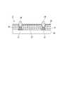
- FIG. 1is a plan view showing a schematic configuration of the element substrate 1
- FIG. 2is an enlarged plan view showing a main part of the element substrate 1.
- a display region 201 for displaying an imageis provided on the surface of the element substrate 1 to which the present invention is applied.
- the display area 201forms a rectangular area as a whole by arranging a plurality of pixels P as a minimum unit of image display in a matrix.
- the display area 201includes a plurality of source bus lines (signal lines) 202 extending in one direction (vertical direction in the figure) and a plurality of gates extending in the other direction (horizontal direction in the figure).
- Bus lines (scanning wirings) 203are arranged in a grid while intersecting each other.
- a region defined by the source bus lines 202 and the gate bus lines 203 arranged in a latticeform one pixel P, and a pixel electrode 204 is disposed in each pixel P.
- each pixel electrode 204is electrically connected to a switching element 205 formed of a thin film transistor (TFT).
- TFTs constituting the switching element 205(referred to as TFT 205 as required) are respectively disposed in the vicinity of the intersection between the source bus line 202 and the gate bus line 203 described above.
- the source S of the TFT 205is formed integrally with the source bus line 202.
- the drain D of the TFT 205is formed integrally with the drain line 207, and the drain line 207 is electrically connected to the pixel electrode 204 via the electrode connection portion 208.
- the gate G of the TFT 205is formed integrally with the gate bus line 203. In the element substrate 1, it is possible to switch on / off (ON / OFF) of the drive voltage applied to each pixel electrode 204 by the switching element 205.
- the display area 201is provided with an auxiliary capacitance wiring 209 facing the pixel electrode 204.
- the auxiliary capacitance wiring 209constitutes an auxiliary capacitance with the pixel electrode 204, and one end thereof is electrically connected to the source bus line 202 via the wiring connection portion 210.
- the alignment direction of the source bus lines 202(horizontal direction in the figure) and the alignment direction of the gate bus lines 203 (vertical direction in the figure) are provided.
- a plurality of wiring terminal portions 211are arranged side by side. One end of each of the source bus line 202 and the gate bus line 203 is electrically connected to the plurality of terminal portions 211.
- peripheral circuit areaalthough not shown, a gate driver, a source driver, a control circuit, etc. are provided as peripheral circuit portions.
- the gate driveris electrically connected to the plurality of gate bus lines 203 through the plurality of wiring terminal portions 211.
- the gate driversequentially supplies scanning signals to the plurality of gate bus lines 203.
- the switching element (TFT) 205is driven in units of horizontal lines.
- the source driveris electrically connected to the plurality of gate bus lines 203 through the plurality of wiring terminal portions 211.
- the source driverconverts the supplied image signal into an analog image signal, and converts the image signal for one horizontal line into a plurality of source bus lines for each horizontal period in which the scanning signal is supplied to the gate bus line 203. 202.
- the control circuitsupplies a control signal for image display to the source driver and the gate driver.
- the control signal supplied to the source driverincludes a source start pulse (SSP), a source shift clock signal (SSC), a source output enable signal (SOE), a polarity control signal (POL), and the like.
- the control signals supplied to the gate driverinclude a gate start pulse (GSP), a gate shift clock signal (GSC), and a gate output enable signal (GOE).
- a TFT (not shown) constituting the peripheral circuit portion and the likeare integrally formed on the same surface together with the TFT constituting the switching element 205 (referred to as monolithic). ).
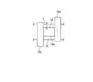
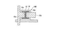
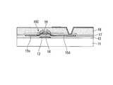
- FIGS. 3A and 3Billustrate an example of a bottom-gate TFT 10 using an oxide semiconductor.
- FIG. 3Ashows a plan view thereof
- FIG. 3Bshows a sectional view thereof.
- the TFT constituting the switching element 205 and the TFT constituting the peripheral circuit portionhave basically the same structure and are formed in the same process. In FIGS. 3A and 3B, these will be collectively described as the TFT 10.
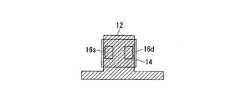
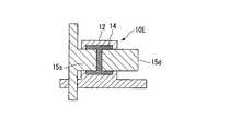
- the TFT 10includes a gate electrode 12, a gate insulating layer 13, an oxide semiconductor layer 14, and a source on the surface of a light-transmitting base material (transparent substrate) 11 such as glass. It has a bottom gate structure in which an electrode 15s and a drain electrode 15d are sequentially stacked.
- the gate electrode 12constitutes a part of the gate bus line 203 and is formed in a stripe shape on the surface of the base material 11.
- a forming material of the gate electrode 12for example, a laminated film of W (tungsten) / TaN (tantalum nitride), Mo (molybdenum), Ti (titanium), Al (aluminum) or Al alloy, Cu (copper) or Cu alloy, etc. Can be used.
- the gate insulating film 13is formed on the surface of the base material 11 so as to cover the gate electrode 12.
- a material for forming the gate insulating film 13for example, an inorganic insulating material such as a silicon nitride film, a silicon oxide film, a silicon nitride oxide film, or a laminated film thereof can be used.
- the oxide semiconductor layer 14is formed in a rectangular shape on the surface of the gate insulating film 13 so as to face the gate electrode 12.
- an oxide semiconductor (InGaZnO) formed of indium (In), gallium (Ga), or zinc (Zn) called IGZOcan be used.
- As the oxide semiconductorin addition to IGZO, for example, an In—Zn—O-based oxide semiconductor composed of indium (In) and zinc (Zn) called IZO, and zinc (Zn) called ZTO are used.
- a Zn—Ti—O-based oxide semiconductor made of titanium (Ti)can be used.
- the source electrode 15 s and the drain electrode 15 dare formed on the etching stopper film 16.
- the etching stopper film 16is formed on the gate insulating film 13 so as to cover the oxide semiconductor layer 14.
- the source electrode 15 s and the drain electrode 15 dare provided in contact with the oxide semiconductor layer 14 through contact holes (contact portions) 16 s and 16 d formed in the etching stopper film 16.
- the source region 14s and the drain region 14dare formed by reducing the resistance of the regions in contact with the source electrode 15s and the drain electrode 15d.
- a region of the oxide semiconductor layer 14 that overlaps with the gate electrode 12 between the source region 14s and the drain region 14dfunctions as the channel region 14c.
- a passivation film 17is formed on the etching stopper film 16 so as to cover the source electrode 15s and the drain electrode 15d.
- a material for forming the passivation film 17the same inorganic insulating material as that for the gate insulating layer 13 can be used.
- An interlayer insulating film 18is formed on the passivation film 16.
- an organic insulating materialsuch as polyimide, polyamide, acrylic, polyimide amide, benzocyclobutene, or the like can be used.
- the scanning signalis supplied to the gate electrode 12 through the gate bus line 203 (gate electrode 12), and the TFT 10 is turned on.
- an image signalflows from the source region 14 s (source electrode 15 s) to the drain region 14 d (drain electrode 15 d) through the channel region 14 c of the oxide semiconductor layer 14 through the source bus line 202 and then to the pixel electrode 204. Supplied.
- 3A and 3Bexemplify the n-channel TFT 10, but the element substrate 1 may use a p-channel TFT.
- 3A and 3Bexemplify the bottom gate type TFT 10, but the element substrate 1 may use a top gate type TFT.
- the degree of shift amount ( ⁇ V th ) of the threshold voltage when voltage stress is applieddiffers depending on the driving voltage and the on / off ratio with respect to the gate electrode 12.
- the driving voltage and the on / off ratioare different between the switching element TFT and the peripheral circuit part TFT described above.
- the TFT for the peripheral circuit sectionhas a higher drive voltage than the TFT for the switching element, and a negative gate bias voltage ( ⁇ Vg) is mainly applied to the TFT for the switching element.
- a positive gate bias voltage (+ Vg)is mainly applied to the TFT for the peripheral circuit section.
- the TFT for the switching element and the TFT for the peripheral circuit sectionhave different threshold voltage shift amounts ( ⁇ V th ) when voltage stress is applied, so that the reliability of both TFTs is ensured when used for a long time. Difficult to do.
- the threshold voltage shift amount ( ⁇ V th )changes.
- FIG. 4Bis a visual graph of the measurement results after 3600 seconds shown in FIG. 4A.
- the shift amount of the threshold voltage ( ⁇ V th ) of the TFT 10is more easily shifted on the plus side than the minus side with respect to a certain initial value (0).
- the threshold voltage shift amount ( ⁇ V th ) of the TFT 10is easily shifted from the plus side to the minus side with respect to a certain initial value (0).
- the shift amount ( ⁇ V th ) of the threshold voltagecan be controlled (optimized) by adjusting the amount of light applied to the oxide semiconductor layer 14. That is, in the TFT 10 using an oxide semiconductor, the threshold voltage shift amount ( ⁇ V th ) is shifted to the positive side by adjusting the amount of light irradiated to the oxide semiconductor layer 14 (in particular, the channel region 14c). It is possible to shift it to the minus side.
- FIG. 6Ashows a change with time of the shift amount ( ⁇ V th ) of the threshold voltage of the TFT 10 shown in FIG. 5A.
- Ashows the change with time of the shift amount ( ⁇ V th ) of the threshold voltage of the TFT 10 shown in FIG. 5A.
- Bshows the change with time of the shift amount ( ⁇ V th ) of the threshold voltage of the TFT 10 shown in FIG. 5B.
- (C)shows the change with time of the shift amount ( ⁇ V th ) of the threshold voltage of the TFT 10 shown in FIG. 5C.
- the degree of overlap L referred to hererepresents the distance between the edge portions of the gate electrode 12 and the oxide semiconductor layer 14 in the same direction.
- the light diffracted at the end of the gate electrode 12is irradiated to the oxide semiconductor layer 14 when light is irradiated from the substrate 11 side.
- the overlapping degree (distance) L of the oxide semiconductor layer 14 with respect to the gate electrode 12is larger in the TFT 10 illustrated in FIG. 5B than in the TFT 10 illustrated in FIG. 5A. Therefore, the amount of light applied to the oxide semiconductor layer 14 is smaller in the TFT 10 illustrated in FIG. 5B than in the TFT 10 illustrated in FIG. 5A. Therefore, in the graph shown in FIG. 6, in the TFT 10 shown in FIG. 5B, the threshold voltage shift amount ( ⁇ V th ) is shifted to the plus side as time passes, compared to the TFT 10 shown in FIG. 5A.
- the degree of overlap (distance) L of the oxide semiconductor layer 14 with respect to the gate electrode 12is smaller in the TFT 10 illustrated in FIG. 5C than in the TFT 10 illustrated in FIG. 5A. Therefore, the amount of light applied to the oxide semiconductor layer 14 is greater in the TFT 10 illustrated in FIG. 5C than in the TFT 10 illustrated in FIG. 5A. For this reason, as shown in FIG. 6, in the TFT 10 shown in FIG. 5C, the threshold voltage shift amount ( ⁇ V th ) is shifted to the minus side as time passes, compared to the TFT 10 shown in FIG. 5A.
- the above-described switching element TFT and the peripheral circuit portion TFThaving different driving voltages and on / off ratios with respect to the gate electrode 12 described above,
- the shift amount ( ⁇ V th ) of the threshold voltagecan be adjusted.
- the peripheral circuit portion TFTis gated more than the switching element TFT, for example.
- the degree of overlap (distance) L of the oxide semiconductor layer 14 with respect to the electrode 12is reduced.
- the switching element TFT and the peripheral circuit portion TFTcan be adjusted.
- the present inventionhas been made on the basis of the above knowledge. At least on the substrate 11, the gate electrode 12, the gate insulating layer 13, the oxide semiconductor layer 14, the source electrode 15s and the drain electrode are provided.
- 15dis an element substrate 1 on which a plurality of TFTs 10 are disposed, and a gate electrode 12, an oxide semiconductor layer 14, and a source between TFTs 10 having different driving voltages or on / off ratios with respect to the gate electrode 12
- the degree of overlap L between the electrode 15s and the drain electrode 15dis different.
- reducing the overlapping degree Lmeans adjusting the overlapping degree L of the channel region 14c with the gate electrode 12 in the direction of increasing the amount of light irradiated to the channel region 14c.
- reducing the overlapping degree Lit is possible to adjust the shift amount ( ⁇ V th ) of the threshold voltage of the TFT in the direction of relatively shifting to the negative side.
- increasing the overlapping degree Lmeans adjusting the overlapping degree L of the channel region 14c with the gate electrode 12 in a direction to reduce the amount of light irradiated to the channel region 14c.
- increasing the degree of overlap Lit is possible to adjust the shift amount ( ⁇ V th ) of the threshold voltage of the TFT in a direction that relatively shifts to the positive side.
- a specific method for adjusting the overlapping degree Lfor example, a method in which the distance between the edge portions in the same direction of the gate electrode 12 and the oxide semiconductor layer 14 is different, A method of varying the distance between the edge portions in the same direction of the channel region 14c and the gate electrode 12 to be formed, a method of varying the overlapping degree of the contact holes 16s and 16d with respect to the edge of the gate electrode 12, and the like. Can be mentioned. Further, these methods can be used alone or in combination.
- the overlapping degree Lis adjusted in the direction in which the distance is relatively short. It is preferable to carry out.
- the TFT 10 in which the drive voltage or the on / off ratio with respect to the gate electrode 12 is relatively lowit is preferable to adjust the overlapping degree L in the direction in which the distance becomes relatively long.
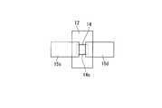
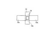
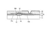
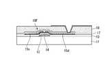
- FIGS. 7A to 7Dexemplify a case where the overlapping degree L is different between the switching element TFT and the peripheral circuit portion TFT. 7A to 7D, the description of the same parts as those of the TFT 10 shown in FIG. 3A is omitted, and the same reference numerals are given.
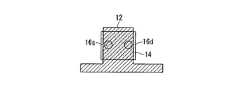
- FIG. 7Ashows a case where the TFT for the switching element has a structure in which the source electrode 15s and the drain electrode 15d are connected to the oxide semiconductor layer 14 through the contact holes 16s and 16d.
- the contact holes 16 s and 16 dare located inside the edge of the gate electrode 12.
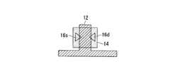
- FIG. 7Bshows the case where the TFT for the peripheral circuit section has a structure in which the source electrode 15s and the drain electrode 15d are connected to the oxide semiconductor layer 14 through the contact holes 16s and 16d.
- the contact holes 16s and 16dare positioned so as to overlap with the edge of the gate electrode 12 in plan view.
- the TFT for the peripheral circuit portion shown in FIG. 7Bis adjusted in a direction in which the degree of overlap L is smaller than the TFT for the switching element shown in FIG. 7A.
- FIG. 7Cshows the case where the switching element TFT has a structure in which the source electrode 15 s and the drain electrode 15 d are directly connected to the oxide semiconductor layer 14.
- FIG. 7Dshows the case where the TFT for the peripheral circuit portion has a structure in which the source electrode 15 s and the drain electrode 15 d are directly connected to the oxide semiconductor layer 14.
- the peripheral circuit portion TFT shown in FIG. 7Dis adjusted in a direction in which the degree of overlap L is smaller than the peripheral circuit portion TFT shown in FIG. 7C.
- the overlapping degree of the contact holes 16s and 16d with respect to the edge of the gate electrode 12is made different by changing the positions and shapes of the contact holes 16s and 16d. Is possible.
- FIGS. 8A to 8Iillustrate cases where the positions and shapes of the contact holes 16s and 16d are different.
- 8A to 8Ithe description of the same part as the TFT 10 shown in FIG. 3A is omitted, and the same reference numerals are given.
- the contact holes 16s and 16d shown in FIGS. 8A to 8Chave a rectangular shape in plan view. Further, the contact holes 16s and 16d shown in FIGS. 8A to 8C exemplify cases in which the overlapping degree with respect to the edge portion of the gate electrode 12 is different.
- the contact holes 16s and 16d shown in FIGS. 8D to 8Fhave a circular shape in plan view. Further, the contact holes 16s and 16d shown in FIGS. 8D to 8F exemplify cases in which the overlapping degrees with respect to the edge portion of the gate electrode 12 are different.
- the contact holes 16s and 16d shown in FIGS. 8G to 8Ihave a triangular shape in plan view. Further, the contact holes 16s and 16d shown in FIGS. 8G to 8I exemplify cases where the overlapping degrees with respect to the edge portion of the gate electrode 12 are different.
- the gate electrode 12, the oxide semiconductor layer 14, the source electrode 15 s, and the drain electrode 15 dare overlapped with each other.
- the threshold voltage shift amount ( ⁇ V th ) due to light irradiation between the TFTs 10 having different drive voltages and on / off ratios with respect to the gate electrode 12by utilizing the characteristic that the threshold voltage shift amount ( ⁇ V th ) of the TFT 10 changes. It is possible to ensure the reliability of each TFT 10 while adjusting th ).
- TFTs 10A to 10F shown in FIGS. 9A to 14Bcan be exemplified.
- 9A, FIG. 9A, FIG. 9A, FIG. 11A, FIG. 12A, FIG. 13A, and FIG. 14Ashow the plan views
- FIG. 9B, FIG. 12B, FIG. 13B, and FIG. 14Bshow sectional views thereof.
- the description of the same part as the TFT 10 shown in FIG. 3Ais omitted, and the same reference numerals are given.
- the oxide semiconductor layer 14is disposed in a region inside the gate electrode 12 so as to overlap the gate electrode 12 in plan view.
- the source electrode 15s and the drain electrode 15dare directly connected to the oxide semiconductor layer 14.
- An etching stopper film 16is disposed only between the source electrode 15s and the drain electrode 15d.
- the rest of the configurationis basically the same as that of the TFT 10 shown in FIG. 3A.
- the oxide semiconductor layer 14is disposed in a region inside the gate electrode 12 so as to overlap the gate electrode 12 in plan view. Further, the source electrode 15 s and the drain electrode 15 d are connected to the oxide semiconductor layer 14 through contact holes (contact portions) 16 s and 16 d formed in the etching stopper film 16. The rest of the configuration is basically the same as that of the TFT 10 shown in FIG. 3A.
- the oxide semiconductor layer 14is disposed so as to overlap the gate electrode 12 in a plan view in a state of protruding outward from the edge of the gate electrode 12.
- the source electrode 15s and the drain electrode 15dare directly connected to the oxide semiconductor layer 14.
- An etching stopper film 16is disposed only between the source electrode 15s and the drain electrode 15d.
- the rest of the configurationis basically the same as that of the TFT 10 shown in FIG. 3A.
- the oxide semiconductor layer 14is disposed so as to overlap the gate electrode 12 in a plan view in a state of protruding outward from the edge of the gate electrode 12.
- the source electrode 15s and the drain electrode 15dare connected to the oxide semiconductor layer 14 through contact holes (contact portions) 16s and 16d formed in the etching stopper film 16.
- the rest of the configurationis basically the same as that of the TFT 10 shown in FIG. 3A.
- the oxide semiconductor layer 14is disposed in a region inside the gate electrode 12 so as to overlap the gate electrode 12 in plan view.
- the source electrode 15s and the drain electrode 15dare directly connected to the oxide semiconductor layer 14. Further, the etching stopper film 16 is omitted.
- the rest of the configurationis basically the same as that of the TFT 10 shown in FIG. 3A.
- the oxide semiconductor layer 14is disposed so as to overlap the gate electrode 12 in a plan view in a state of protruding outward from the edge of the gate electrode 12.
- the source electrode 15s and the drain electrode 15dare directly connected to the oxide semiconductor layer 14. Further, the etching stopper film 16 is omitted.
- the rest of the configurationis basically the same as that of the TFT 10 shown in FIG. 3A.
- the element substrate 1is not necessarily limited to the configuration in which the overlapping degree L is different between the switching element TFT and the peripheral circuit portion TFT described above.
- the peripheral circuit areais provided with peripheral circuit portions such as the gate driver, source driver, and control circuit described above, the driving voltage for the gate electrode 12 and the like between the TFTs constituting these peripheral circuit portions are The on / off ratio may be different.
- the liquid crystal display deviceis schematically configured by combining a liquid crystal display panel, a backlight, a pair of polarizing plates (not shown), and the like.
- this liquid crystal display deviceit is possible to visually recognize an image displayed on the liquid crystal display panel by irradiating the liquid crystal display panel with illumination light emitted from the backlight.
- the element substrate 1is used in a liquid crystal display panel provided in the liquid crystal display device.
- the liquid crystal display panelincludes the element substrate 1 and the counter substrate 2 shown in FIG.
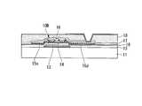
- FIG. 15is a cross-sectional view showing a schematic configuration of the counter substrate 2.
- the counter substrate 2is a light shield that partitions a region corresponding to the pixel electrode 204 (pixel P) on the surface of a light-transmitting base material (transparent substrate) 20 such as glass.
- a photo spacer 24for maintaining a gap (cell gap) between the two.
- a liquid crystal display panelafter forming an orientation film in the mutually opposing surface of the element substrate 1 and the counter substrate 2, the element substrate 1 and the counter substrate 2 are made to oppose each other, and a liquid crystal is provided between them. After the injection, the periphery between them is sealed with a seal member. As a result, a liquid crystal display panel in which the liquid crystal layer is sandwiched between the element substrate 1 and the counter substrate 2 can be obtained.
- the liquid crystal display deviceby using the element substrate 1 for the liquid crystal display panel, it is possible to perform stable and reliable display.
- the element substrate 1 for a liquid crystal display devicehas been described as an example.
- the display device to which the present invention is appliedis not limited to the above-described liquid crystal display device, for example, an element substrate and a counter substrate.
- ELorganic electroluminescence
- an element substratecapable of ensuring the reliability of each thin film transistor even when the driving voltage and the on / off ratio with respect to the gate electrode are different.
Landscapes
- Liquid Crystal (AREA)
- Thin Film Transistor (AREA)
Abstract
Description
Translated fromJapanese 本発明は、素子基板及び表示装置に関する。
本願は、2012年10月5日に、日本に出願された特願2012-223549号に基づき優先権を主張し、その内容をここに援用する。The present invention relates to an element substrate and a display device.
This application claims priority based on Japanese Patent Application No. 2012-223549 filed in Japan on October 5, 2012, the contents of which are incorporated herein by reference.
近年、液晶表示装置の開発が盛んに行われている。その中でも、アクティブマトリクス駆動方式を採用した液晶表示パネルを備えたものが主流となっている。具体的に、この液晶表示パネルは、互いに対向配置された素子基板及び対向基板と、これら素子基板と対向基板との間に挟持された液晶層とを備えている。In recent years, liquid crystal display devices have been actively developed. Among them, those equipped with a liquid crystal display panel adopting an active matrix driving method are mainstream. Specifically, the liquid crystal display panel includes an element substrate and a counter substrate that are arranged to face each other, and a liquid crystal layer that is sandwiched between the element substrate and the counter substrate.
このうち、素子基板の液晶層と対向する面上には、画像表示の単位画素となる複数の画素電極がマトリクス状に配置されることによって、画像を表示するための表示領域が形成されている。また、各画素電極には、薄膜トランジスタ(TFT:Thin Film Transistor)などのスイッチング素子が接続されており、このスイッチング素子によって各画素電極に印加される駆動電圧のオン/オフ(ON/OFF)を切り換えることが可能となっている。Among these, on the surface facing the liquid crystal layer of the element substrate, a plurality of pixel electrodes serving as unit pixels for image display are arranged in a matrix to form a display region for displaying an image. . Each pixel electrode is connected to a switching element such as a thin film transistor (TFT), and the switching element switches on / off of the drive voltage applied to each pixel electrode. It is possible.
また、素子基板の表示領域の周辺(周辺回路領域という。)には、周辺回路部が設けられている。この周辺回路部は、ソースバスラインと電気的に接続されたソースドライバや、ゲートバスラインと電気的に接続されたゲートドライバなどからなる。また、液晶表示パネルでは、上述したスイッチング素子用のTFTと共に、この周辺回路部を構成するTFTなどを素子基板上に一体に形成することも行われている(モノリシック化という。)。Further, a peripheral circuit section is provided around the display area of the element substrate (referred to as a peripheral circuit area). The peripheral circuit section includes a source driver electrically connected to the source bus line, a gate driver electrically connected to the gate bus line, and the like. In addition, in the liquid crystal display panel, the TFT for constituting the peripheral circuit portion and the like are integrally formed on the element substrate together with the TFT for the switching element described above (referred to as monolithic).
一方、対向基板の液晶層と対向する面上には、上述した複数の画素電極と対向するベタの対向電極(即ち、複数の画素電極と対向する一つの対向電極)や、各画素電極に対応した領域(画素領域という。)を区画するブラックマトリックス層、このブラックマトリックス層によって区画された領域の内側に埋め込まれたカラーフィルタ層などが設けられている。On the other hand, on the surface of the counter substrate facing the liquid crystal layer, it corresponds to the above-described solid counter electrode facing the plurality of pixel electrodes (that is, one counter electrode facing the plurality of pixel electrodes) or each pixel electrode. A black matrix layer that partitions the region (referred to as a pixel region), a color filter layer that is embedded inside the region partitioned by the black matrix layer, and the like are provided.
ところで、最近では、従来の非晶質シリコン(a-Si)や多結晶シリコン(p-Si)に代わって、酸化物半導体を用いたTFTが次世代ディスプレイに応用できる半導体素子として注目されている(例えば、特許文献1~6を参照。)。Recently, TFTs using oxide semiconductors are attracting attention as semiconductor elements that can be applied to next-generation displays in place of conventional amorphous silicon (a-Si) and polycrystalline silicon (p-Si). (For example, see
具体的に、酸化物半導体としては、例えばIGZOと呼ばれるインジウム(In)、ガリウム(Ga)、亜鉛(Zn)で構成された酸化物半導体(InGaZnO)を挙げることができる。この酸化物半導体は、a-Siよりも高い移動度を有している。このため、酸化物半導体を用いたTFTでは、a-Siを用いたTFTよりも高速で動作させることが可能である。また、酸化物半導体は、p-Siよりも簡便なプロセスで形成されるため、大面積が必要とされる表示装置等にも適用可能である。このため、上述した液晶表示パネルだけでなく、有機ELパネルや電子ペーパーなどの次世代ディスプレイへの応用が期待されている。Specifically, as an oxide semiconductor, for example, an oxide semiconductor (InGaZnO) formed of indium (In), gallium (Ga), and zinc (Zn) called IGZO can be given. This oxide semiconductor has higher mobility than a-Si. Therefore, a TFT using an oxide semiconductor can be operated at a higher speed than a TFT using a-Si. In addition, an oxide semiconductor is formed by a simpler process than p-Si, and thus can be applied to a display device or the like that requires a large area. For this reason, the application to not only the liquid crystal display panel mentioned above but next-generation displays, such as an organic electroluminescent panel and electronic paper, is anticipated.
しかしながら、酸化物半導体のキャリア生成メカニズムは、a-Siやp-Siといったシリコン系半導体とは大きく異なっているため、酸化物半導体特有の物性がTFTの特性や信頼性に大きな影響を及ぼすことがある。However, the carrier generation mechanism of oxide semiconductors is significantly different from that of silicon-based semiconductors such as a-Si and p-Si, and physical properties peculiar to oxide semiconductors have a great influence on TFT characteristics and reliability. is there.
例えば、IGZOを用いたTFTでは、光照射環境でのバイアスストレスの挙動がa-Siを用いたTFTとは異なるといった特徴がある。具体的に、IGZOを用いたTFTでは、正のゲートバイアス電圧(+Vg)を印加したときに、光照射により閾値電圧のシフト量(ΔVth)が小さくなる。一方、TFTに負のゲートバイアス電圧(-Vg)を印加したときには、光照射により閾値電圧のシフト量(ΔVth)が大きくなる。For example, a TFT using IGZO has a feature that the behavior of bias stress in a light irradiation environment is different from that of a TFT using a-Si. Specifically, in a TFT using IGZO, when a positive gate bias voltage (+ Vg) is applied, the threshold voltage shift amount (ΔVth ) is reduced by light irradiation. On the other hand, when a negative gate bias voltage (−Vg) is applied to the TFT, the threshold voltage shift amount (ΔVth ) increases due to light irradiation.
また、IGZOを用いたTFTでは、ゲート電極に対する駆動電圧やオン/オフ比の違いによって信頼性の劣化の仕方が異なる。特に、上述した素子基板上に形成されたスイッチング素子用のTFTと周辺回路部用のTFTとの間では、駆動電圧及びオン/オフ比が異なっている。このため、両方のTFTの信頼性を確保することが困難であった。Further, in the TFT using IGZO, the method of deterioration of reliability differs depending on the driving voltage and the on / off ratio with respect to the gate electrode. In particular, the driving voltage and the on / off ratio are different between the switching element TFT and the peripheral circuit TFT formed on the element substrate. For this reason, it has been difficult to ensure the reliability of both TFTs.
なお、オン/オフ比とは、ゲート電極に印加される駆動電圧のうち、オン状態で印加される電圧(Vgh)の印加時間と、オフ状態で印加される電圧(Vgl)の印加時間とのデューティ比のことを言う。すなわち、ここで言うオン/オフ比は、ゲートパルスの周波数のことを意味する。The on / off ratio refers to the application time of the voltage (Vgh ) applied in the on state and the application time of the voltage (Vgl ) applied in the off state among the driving voltages applied to the gate electrode. And the duty ratio. That is, the on / off ratio referred to here means the frequency of the gate pulse.
本発明は、このような従来の事情に鑑みて提案されたものであり、素子基板上に配置された複数の薄膜トランジスタの間でゲート電極に対する駆動電圧やオン/オフ比が異なる場合であっても、それぞれの薄膜トランジスタの信頼性を確保することを可能とした素子基板、並びにこのような素子基板を用いた表示装置を提供することを目的とする。The present invention has been proposed in view of such a conventional situation, and even when the driving voltage and the on / off ratio with respect to the gate electrode are different among the plurality of thin film transistors arranged on the element substrate. An object of the present invention is to provide an element substrate capable of ensuring the reliability of each thin film transistor and a display device using such an element substrate.
上記目的を達成するために、本発明に係る素子基板は、少なくとも基材の上に、ゲート電極と、ゲート絶縁層と、酸化物半導体層と、ソース電極及びドレイン電極とを積層した複数の薄膜トランジスタが配置された素子基板であって、ゲート電極に対する駆動電圧又はオン/オフ比が異なる薄膜トランジスタの間で、ゲート電極と、酸化物半導体層と、ソース電極及びドレイン電極との何れかの重なり度合いを異ならせていることを特徴とする。In order to achieve the above object, an element substrate according to the present invention includes a plurality of thin film transistors in which a gate electrode, a gate insulating layer, an oxide semiconductor layer, and a source electrode and a drain electrode are stacked on at least a base material. Between the thin film transistors having different drive voltages or on / off ratios with respect to the gate electrode, the degree of overlap of the gate electrode, the oxide semiconductor layer, the source electrode, and the drain electrode. It is characterized by being different.
以上のような構成を備える素子基板では、酸化物半導体層に光が照射されたときに、ゲート電極と、酸化物半導体層と、ソース電極及びドレイン電極との重ね合わせの違いによって、薄膜トランジスタの閾値電圧のシフト量(ΔVth)が変化する特性を利用して、ゲート電極に対する駆動電圧又はオン/オフ比が異なる薄膜トランジスタの間で、光照射による閾値電圧のシフト量(ΔVth)を調整しながら、それぞれの薄膜トランジスタの信頼性を確保することが可能である。In the element substrate having the above structure, when the oxide semiconductor layer is irradiated with light, the threshold value of the thin film transistor depends on a difference in overlap between the gate electrode, the oxide semiconductor layer, and the source electrode and the drain electrode. Using the characteristic that the voltage shift amount (ΔVth ) changes, the threshold voltage shift amount (ΔVth ) due to light irradiation is adjusted between thin film transistors having different driving voltages or on / off ratios with respect to the gate electrode. The reliability of each thin film transistor can be ensured.
また、上記素子基板では、ゲート電極と酸化物半導体層との互いの同一方向における端縁部同士の距離を異ならせている構成であればよい。The element substrate may have a configuration in which the distance between the edge portions in the same direction of the gate electrode and the oxide semiconductor layer is different.
この構成の場合、ゲート電極に対する駆動電圧又はオン/オフ比が異なる薄膜トランジスタの間で、ゲート電極と酸化物半導体層との重ね合わせ度合いを異ならせることによって、光照射による閾値電圧のシフト量(ΔVth)を調整し、それぞれの薄膜トランジスタの信頼性を確保することが可能である。In the case of this configuration, the threshold voltage shift amount (ΔV) due to light irradiation is changed by changing the overlapping degree of the gate electrode and the oxide semiconductor layer between thin film transistors having different driving voltages or on / off ratios with respect to the gate electrode.th ) can be adjusted to ensure the reliability of each thin film transistor.
また、上記素子基板では、酸化物半導体層に形成されるチャネル領域と、ゲート電極との互いの同一方向における端縁部同士の距離を異ならせている構成であればよい。Further, the element substrate may have a structure in which the distance between the edge portions in the same direction of the channel region formed in the oxide semiconductor layer and the gate electrode is different.
この構成の場合、ゲート電極に対する駆動電圧又はオン/オフ比が異なる薄膜トランジスタの間で、酸化物半導体層に形成されるチャネル領域と、ゲート電極との重ね合わせ度合いを異ならせることによって、光照射による閾値電圧のシフト量(ΔVth)を調整し、それぞれの薄膜トランジスタの信頼性を確保することが可能である。In the case of this structure, the thin film transistors having different driving voltages or on / off ratios with respect to the gate electrode are different from each other in light irradiation by varying the degree of overlap between the channel region formed in the oxide semiconductor layer and the gate electrode. It is possible to secure the reliability of each thin film transistor by adjusting the shift amount (ΔVth ) of the threshold voltage.
また、上記素子基板では、複数の薄膜トランジスタのうち、ゲート電極に対する駆動電圧又はオン/オフ比が相対に高くなる薄膜トランジスタに対しては、上記距離が相対的に短くなる方向に重なり度合いの調整が行われ、ゲート電極に対する駆動電圧又はオン/オフ比が相対に低くなる薄膜トランジスタに対しては、上記距離が相対的に長くなる方向に重なり度合いの調整が行われていることが好ましい。In the element substrate, among the plurality of thin film transistors, the degree of overlap is adjusted in the direction in which the distance is relatively shortened for a thin film transistor having a relatively high driving voltage or on / off ratio with respect to the gate electrode. In other words, it is preferable that the degree of overlap be adjusted in the direction in which the distance becomes relatively long for the thin film transistor in which the drive voltage or the on / off ratio with respect to the gate electrode is relatively low.
これにより、ゲート電極に対する駆動電圧又はオン/オフ比が異なる薄膜トランジスタの間で、光照射による閾値電圧のシフト量(ΔVth)を調整し、それぞれの薄膜トランジスタの信頼性を確保することが可能である。This makes it possible to adjust the shift amount (ΔVth ) of the threshold voltage due to light irradiation between thin film transistors having different driving voltages or on / off ratios with respect to the gate electrode, and to ensure the reliability of each thin film transistor. .
また、上記素子基板では、ソース電極及びドレイン電極が、一対のコンタクト部を介して酸化物半導体層と電気的に接続されており、一対のコンタクト部のゲート電極の端縁部に対する重なり度合いを異ならせている構成であってもよい。In the element substrate, the source electrode and the drain electrode are electrically connected to the oxide semiconductor layer through the pair of contact portions, and the overlapping degree of the pair of contact portions with respect to the edge portion of the gate electrode is different. It may be a configuration.
この構成の場合、ゲート電極に対する駆動電圧又はオン/オフ比が異なる薄膜トランジスタの間で、一対のコンタクト部のゲート電極の端縁部に対する重なり度合いを異ならせることによって、光照射による閾値電圧のシフト量(ΔVth)を調整し、それぞれの薄膜トランジスタの信頼性を確保することが可能である。In this configuration, the threshold voltage shift amount due to light irradiation is changed by varying the overlapping degree of the pair of contact portions with respect to the edge of the gate electrode between thin film transistors having different driving voltages or on / off ratios with respect to the gate electrode. By adjusting (ΔVth ), the reliability of each thin film transistor can be ensured.
また、上記素子基板では、一対のコンタクト部の位置を異ならせている構成であってもよい。Further, the element substrate may have a configuration in which the positions of the pair of contact portions are different.
この構成の場合、一対のコンタクト部の位置を異ならせることで、一対のコンタクト部のゲート電極の端縁部に対する重なり度合いを調整することができる。In this configuration, the overlapping degree of the pair of contact portions with respect to the edge of the gate electrode can be adjusted by changing the positions of the pair of contact portions.
また、上記素子基板では、一対のコンタクト部の形状を異ならせている構成であってもよい。Further, the element substrate may have a configuration in which the shapes of the pair of contact portions are different.
この構成の場合、一対のコンタクト部の形状を異ならせることで、一対のコンタクト部のゲート電極の端縁部に対する重なり度合いを調整することができる。In this configuration, the overlapping degree of the pair of contact portions with respect to the edge of the gate electrode can be adjusted by changing the shapes of the pair of contact portions.
また、上記素子基板では、基材の面内に、表示領域と、この表示領域の周辺に周辺回路領域とが設けられ、表示領域に設けられた薄膜トランジスタと、周辺回路領域に設けられた薄膜トランジスタとの間で、上記重なり度合いを異ならせている構成であってもよい。In the element substrate, a display region is provided in the surface of the base material, and a peripheral circuit region is provided around the display region. A thin film transistor provided in the display region, a thin film transistor provided in the peripheral circuit region, and The degree of overlapping may be different between the two.
この構成の場合、表示領域に設けられた薄膜トランジスタと、周辺回路領域に設けられた薄膜トランジスタとの間で、光照射による閾値電圧のシフト量(ΔVth)を調整しながら、それぞれの薄膜トランジスタの信頼性を確保することが可能である。In this configuration, the reliability of each thin film transistor is adjusted while adjusting the shift amount (ΔVth ) of the threshold voltage due to light irradiation between the thin film transistor provided in the display region and the thin film transistor provided in the peripheral circuit region. Can be secured.
また、上記素子基板では、更に、周辺回路領域に設けられた薄膜トランジスタの間で、上記重なり度合いを異ならせている構成であってもよい。Further, the element substrate may be configured such that the degree of overlap is different between the thin film transistors provided in the peripheral circuit region.
この構成の場合、周辺回路領域に設けられた薄膜トランジスタの間で、光照射による閾値電圧のシフト量(ΔVth)を調整しながら、それぞれの薄膜トランジスタの信頼性を確保することが可能である。In the case of this configuration, it is possible to ensure the reliability of each thin film transistor while adjusting the shift amount (ΔVth ) of the threshold voltage due to light irradiation between the thin film transistors provided in the peripheral circuit region.
また、上記素子基板では、薄膜トランジスタが、基材の上に、ゲート電極と、ゲート絶縁層と、酸化物半導体層と、ソース電極及びドレイン電極とを順次積層したボトムゲート構造を有する構成であってもよい。In the element substrate, the thin film transistor has a bottom gate structure in which a gate electrode, a gate insulating layer, an oxide semiconductor layer, a source electrode, and a drain electrode are sequentially stacked on a base material. Also good.
この構成の場合、薄膜トランジスタがボトムゲート構造を有する構成において、ゲート電極に対する駆動電圧やオン/オフ比が異なる場合であっても、それぞれの薄膜トランジスタの信頼性を確保することが可能である。In the case of this configuration, in the configuration in which the thin film transistor has a bottom gate structure, the reliability of each thin film transistor can be ensured even when the driving voltage and the on / off ratio with respect to the gate electrode are different.
また、上記素子基板では、基材が、光透過性を有する構成であってもよい。Further, in the element substrate, the base material may have a light transmissive structure.
この構成の場合、基材を透過した光が酸化物半導体層に照射される構成において、ゲート電極に対する駆動電圧又はオン/オフ比が異なる薄膜トランジスタの間で、それぞれの薄膜トランジスタの信頼性を確保することが可能である。In the case of this structure, the reliability of each thin film transistor is ensured between thin film transistors having different driving voltages or on / off ratios with respect to the gate electrode in a structure in which light transmitted through the base material is irradiated on the oxide semiconductor layer. Is possible.
また、本発明に係る表示装置は、上記何れかの素子基板と、素子基板に対向して配置された対向基板と、素子基板と対向基板との間に配置された液晶層、有機電界発光層、電気泳動層のうち何れか1つとを備えることを特徴とする。The display device according to the present invention includes any one of the above element substrates, a counter substrate disposed to face the element substrate, a liquid crystal layer disposed between the element substrate and the counter substrate, and an organic electroluminescent layer. And any one of the electrophoretic layers.
以上のような構成を備える表示装置では、上記何れかの素子基板を備えることで、液晶層、有機電界発光層、電気泳動層のうち何れかを用いた信頼性の高い安定した表示を行うことが可能である。In the display device having the above-described configuration, any one of the element substrates described above is provided, so that reliable and stable display using any one of the liquid crystal layer, the organic electroluminescent layer, and the electrophoretic layer is performed. Is possible.
以上のように、本発明によれば、素子基板上に配置された複数の薄膜トランジスタの間でゲート電極に対する駆動電圧やオン/オフ比が異なる場合であっても、それぞれの薄膜トランジスタの信頼性を確保することを可能とした素子基板、並びにこのような素子基板を用いた表示装置を提供することが可能である。As described above, according to the present invention, the reliability of each thin film transistor is ensured even when the driving voltage and the on / off ratio with respect to the gate electrode are different among the plurality of thin film transistors arranged on the element substrate. It is possible to provide an element substrate that can be used and a display device using such an element substrate.
以下、本発明を適用した素子基板及び表示装置について、図面を参照して詳細に説明する。
なお、以下の説明で用いる図面は、特徴をわかりやすくするために、便宜上特徴となる部分を拡大して示している場合があり、各構成要素の寸法比率などが実際と同じであるとは限らない。また、以下の説明において例示される材料、寸法等は一例であって、本発明はそれらに必ずしも限定されるものではなく、その要旨を変更しない範囲で適宜変更して実施することが可能である。Hereinafter, an element substrate and a display device to which the present invention is applied will be described in detail with reference to the drawings.
In addition, in the drawings used in the following description, in order to make the features easy to understand, there are cases where the portions that become the features are enlarged for the sake of convenience, and the dimensional ratios of the respective components are not always the same as the actual ones. Absent. In addition, the materials, dimensions, and the like exemplified in the following description are merely examples, and the present invention is not necessarily limited thereto, and can be appropriately modified and implemented without departing from the scope of the invention. .
[素子基板]
先ず、本発明を適用した素子基板の一実施形態として、例えば図1及び図2に示す液晶表示装置用の素子基板1を例に挙げて説明する。
なお、図1は、この素子基板1の概略構成を示す平面図であり、図2は、この素子基板1の要部を拡大して示す平面図である。[Element substrate]
First, as an embodiment of an element substrate to which the present invention is applied, for example, an
FIG. 1 is a plan view showing a schematic configuration of the
本発明を適用した素子基板1の面上には、図1及び図2に示すように、画像を表示するための表示領域201が設けられている。この表示領域201は、画像表示の最小単位となる画素Pがマトリクス状に複数配置されることによって、全体として矩形状の領域を形成している。As shown in FIGS. 1 and 2, a
この表示領域201には、一の方向(図中の縦方向)に延在する複数のソースバスライン(信号配線)202と、他の方向(図中の横方向)に延在する複数のゲートバスライン(走査配線)203とが、互いに交差しながら格子状に並んで配置されている。そして、これら格子状に並ぶソースバスライン202とゲートバスライン203によって区画された領域が1つの画素Pを構成しており、各画素Pには、画素電極204が配置されている。The
また、各画素電極204には、薄膜トランジスタ(TFT:Thin Film Transistor)からなるスイッチング素子205が電気的に接続されている。このスイッチング素子205を構成するTFT(必要に応じてTFT205と表すものとする。)は、上述したソースバスライン202とゲートバスライン203との交差部近傍にそれぞれ配置されている。
また、このTFT205のソースSは、上記ソースバスライン202と一体に形成されている。一方、このTFT205のドレインDは、ドレインライン207と一体に形成されており、このドレインライン207は、電極接続部208を介して画素電極204と電気的に接続されている。一方、このTFT205のゲートGは、上記ゲートバスライン203と一体に形成されている。そして、素子基板1では、このスイッチング素子205によって各画素電極204に印加される駆動電圧のオン/オフ(ON/OFF)を切り換えることが可能となっている。In addition, each
The source S of the
表示領域201には、上記画素電極204と対向する補助容量配線209が設けられている。この補助容量配線209は、上記画素電極204との間で補助容量を構成するものであり、その一端が配線接続部210を介してソースバスライン202と電気的に接続されている。The
表示領域201の外側の領域(周辺回路領域という。)には、上記ソースバスライン202の並び方向(図中の横方向)及び上記ゲートバスライン203の並び方向(図中の縦方向)に沿って複数の配線端子部211が並んで配置されている。そして、これら複数の端子部211には、それぞれソースバスライン202及びゲートバスライン203の一端が電気的に接続されている。In an area outside the display area 201 (referred to as a peripheral circuit area), the alignment direction of the source bus lines 202 (horizontal direction in the figure) and the alignment direction of the gate bus lines 203 (vertical direction in the figure) are provided. A plurality of wiring
また、周辺回路領域には、図示を省略するものの、周辺回路部としてのゲートドライバやソースドライバ、制御回路などが設けられている。In the peripheral circuit area, although not shown, a gate driver, a source driver, a control circuit, etc. are provided as peripheral circuit portions.
このうち、ゲートドライバは、上記複数の配線端子部211を介して上記複数のゲートバスライン203と電気的に接続されている。そして、このゲートドライバは、複数のゲートバスライン203に走査信号を順次的に供給する。この走査信号に応答して、上記スイッチング素子(TFT)205が水平ライン単位で駆動される。Among these, the gate driver is electrically connected to the plurality of
一方、ソースドライバは、上記複数の配線端子部211を介して上記複数のゲートバスライン203と電気的に接続されている。そして、このソースドライバは、供給された画像信号をアナログ画像信号に変換し、ゲートバスライン203に走査信号が供給される1水平期間毎に、1水平ライン分の画像信号を複数のソースバスライン202に供給する。On the other hand, the source driver is electrically connected to the plurality of
一方、制御回路は、画像表示を行うための制御信号をソースドライバ及びゲートドライバに供給する。具体的に、ソースドライバに供給される制御信号には、ソース・スタートパルス(SSP)、ソース・シフト・クロック信号(SSC)、ソース出力イネーブル信号(SOE)、極性制御信号(POL)等が含まれる。一方、ゲートドライバに供給される制御信号には、ゲート・スタートパルス(GSP)、ゲート・シフト・クロック信号(GSC)、ゲート出力イネーブル信号(GOE)が含まれる。On the other hand, the control circuit supplies a control signal for image display to the source driver and the gate driver. Specifically, the control signal supplied to the source driver includes a source start pulse (SSP), a source shift clock signal (SSC), a source output enable signal (SOE), a polarity control signal (POL), and the like. It is. On the other hand, the control signals supplied to the gate driver include a gate start pulse (GSP), a gate shift clock signal (GSC), and a gate output enable signal (GOE).
素子基板1では、上記スイッチング素子205を構成するTFTと共に、上記周辺回路部を構成するTFT(図示せず。)などを同一面上に一体に形成することが行われている(モノリシック化という。)。In the
[薄膜トランジスタ]
次に、上記素子基板1が備えるTFTの具体的な構成について、例えば図3A及び図3Bに示すTFT10を例に挙げて説明する。
なお、図3A及び図3Bは、酸化物半導体を用いたボトムゲート型のTFT10の一例を示す。図3Aはその平面図を示し、図3Bはその断面図を示す。[Thin film transistor]
Next, a specific configuration of the TFT included in the
3A and 3B illustrate an example of a
なお、上記素子基板1において、上記スイッチング素子205を構成するTFTと、上記周辺回路部を構成するTFTとは、基本的に同じ構造を有しており、同一プロセス中で形成されることから、図3A及び図3Bにおいては、これらをTFT10としてまとめて説明するものとする。In the
TFT10は、図3Bに示すように、例えばガラスなどの光透過性を有する基材(透明基板)11の面上に、ゲート電極12と、ゲート絶縁層13と、酸化物半導体層14と、ソース電極15s及びドレイン電極15dとを順次積層したボトムゲート構造を有している。As shown in FIG. 3B, the
ゲート電極12は、上記ゲートバスライン203の一部を構成するものであり、基材11の面上にストライプ状に形成されている。ゲート電極12の形成材料としては、例えばW(タングステン)/TaN(窒化タンタル)の積層膜、Mo(モリブデン)、Ti(チタン)、Al(アルミニウム)又はAl合金、Cu(銅)又はCu合金等を用いることができる。The
ゲート絶縁膜13は、ゲート電極12を覆うように基材11の面上に形成されている。
このゲート絶縁膜13の形成材料としては、例えば窒化シリコン膜、酸化シリコン膜、窒化酸化シリコン膜又はこれらの積層膜等の無機絶縁性材料を用いることができる。The
As a material for forming the
酸化物半導体層14は、ゲート電極12と対向するようにゲート絶縁膜13の面上に矩形状に形成されている。この酸化物半導体層14の形成材料としては、例えばIGZOと呼ばれるインジウム(In)、ガリウム(Ga)、亜鉛(Zn)で構成された酸化物半導体(InGaZnO)を用いることができる。また、酸化物半導体としては、IGZOの他にも、例えば、IZOと呼ばれるインジウム(In)及び亜鉛(Zn)から構成されたIn-Zn-O系酸化物半導体や、ZTOと呼ばれる亜鉛(Zn)及びチタン(Ti)から構成されたZn-Ti-O系酸化物半導体などを用いることができる。The
ソース電極15s及びドレイン電極15dは、エッチングストッパー膜16上に形成されている。このエッチングストッパー膜16は、酸化物半導体層14を覆うようにゲート絶縁膜13上に形成されている。そして、ソース電極15s及びドレイン電極15dは、エッチングストッパー膜16に形成されたコンタクトホール(コンタクト部)16s,16dを介して酸化物半導体層14に接触した状態で設けられている。The source electrode 15 s and the
また、酸化物半導体層14には、上記ソース電極15s及びドレイン電極15dと接触する領域を低抵抗化させることによって、ソース領域14s及びドレイン領域14dが形成されている。そして、このTFT10では、酸化物半導体層14のうちソース領域14sとドレイン領域14dとの間の上記ゲート電極12と重なる領域がチャネル領域14cとして機能することになる。In the
エッチングストッパー膜16上には、ソース電極15s及びドレイン電極15dを覆うようにパッシベーション膜17が形成されている。このパッシベーション膜17の形成材料としては、上記ゲート絶縁層13と同様の無機絶縁性材料を用いることができる。A
パッシベーション膜16上には、層間絶縁膜18が形成されている。この層間絶縁膜18の形成材料としては、例えばポリイミド、ポリアミド、アクリル、ポリイミドアミド、ベンゾシクロブテン等の有機絶縁性材料を用いることができる。An interlayer insulating
以上のような構造を有するTFT10では、ゲートバスライン203(ゲート電極12)を通じて走査信号がゲート電極12に供給されることによって、オン状態となる。このとき、ソースバスライン202を通じて画像信号が、酸化物半導体層14のチャネル領域14cを介してソース領域14s(ソース電極15s)からドレイン領域14d(ドレイン電極15d)へと流れ込み、画素電極204へと供給される。In the
なお、図3A及び3Bでは、nチャネル型のTFT10を例示したが、上記素子基板1では、pチャネル型のTFTを用いることも可能である。また、図3A及び3Bでは、ボトムゲート型のTFT10を例示したが、上記素子基板1では、トップゲート型のTFTを用いることも可能である。3A and 3B exemplify the n-
[本発明の基本的原理]
次に、本発明の基本的原理について説明する。
上記素子基板1では、上記スイッチング素子205を構成するTFTや、上記周辺回路部を構成するTFT(図示せず。)など、酸化物半導体を用いた複数のTFT10が配置されている。[Basic Principle of the Present Invention]
Next, the basic principle of the present invention will be described.
In the
ここで、酸化物半導体を用いたTFT10では、ゲート電極12に対する駆動電圧やオン/オフ比の違いによって、電圧ストレス印加時の閾値電圧のシフト量(ΔVth)の度合いが異なっている。Here, in the
例えば、上記素子基板1では、上述したスイッチング素子用のTFTと周辺回路部用のTFTとの間で駆動電圧やオン/オフ比が異なっている。具体的に、上記周辺回路部用のTFTは、上記スイッチング素子用のTFTよりも駆動電圧が高く、上記スイッチング素子用のTFTには、負のゲートバイアス電圧(-Vg)がメインで印加されるのに対して、上記周辺回路部用のTFTには、正のゲートバイアス電圧(+Vg)がメインで印加される。For example, in the
したがって、スイッチング素子用のTFTと周辺回路部用のTFTでは、電圧ストレス印加時の閾値電圧のシフト量(ΔVth)が異なるために、長時間使用した場合に、両方のTFTの信頼性を確保することが困難となる。Therefore, the TFT for the switching element and the TFT for the peripheral circuit section have different threshold voltage shift amounts (ΔVth ) when voltage stress is applied, so that the reliability of both TFTs is ensured when used for a long time. Difficult to do.
一方、酸化物半導体を用いたTFT10は、酸化物半導体層14に光が照射されたときに、ゲート電極12と、酸化物半導体層14と、ソース電極15s及びドレイン電極15dとの重ね合わせの違いによって、閾値電圧のシフト量(ΔVth)が変化するといった特性を有している。On the other hand, in the
具体的に、この酸化物半導体を用いたTFT10について、正のゲートバイアス電圧(Vg=+30V)を印加したときの光照射がない場合及び光照射がある場合と、負のゲートバイアス電圧(Vg=-30V)を印加したときの光照射がない場合及び光照射がある場合について、それぞれ閾値電圧のシフト量(ΔVth)の経時的な変化を測定した。その測定結果を図4A及び図4Bに示す。図4A中、符号101は、TFT10に対して正のゲートバイアス電圧(Vg=+30V)を印加し、光照射がない場合における閾値電圧のシフト量(ΔVth)の経時的な変化を示す。符号101は、TFT10に対して正のゲートバイアス電圧(Vg=+30V)を印加し、光照射がある場合における閾値電圧のシフト量(ΔVth)の経時的な変化を示す。符号103は、TFT10に対して負のゲートバイアス電圧(Vg=-30V)を印加し、光照射がない場合における閾値電圧のシフト量(ΔVth)の経時的な変化を示す。符号104は、TFT10に対して負のゲートバイアス電圧(Vg=-30V)を印加し、光照射がある場合における閾値電圧のシフト量(ΔVth)の経時的な変化を示す。なお、図4Bは、図4Aに示す3600秒後における測定結果について、視覚的にグラフ化したものである。Specifically, for the
図4A及び図4Bに示すように、光照射がない場合は、TFT10の閾値電圧のシフト量(ΔVth)がある初期値(0)に対してマイナス側よりもプラス側がシフトし易くなっている。一方、このTFT10に光を照射したときには、TFT10の閾値電圧のシフト量(ΔVth)がある初期値(0)に対してプラス側よりもマイナス側にシフトし易くなる。As shown in FIG. 4A and FIG. 4B, when there is no light irradiation, the shift amount of the threshold voltage (ΔVth ) of the
これは、酸化物半導体層14に照射される光の量を調整することで、閾値電圧のシフト量(ΔVth)を制御(最適化)できることを表している。すなわち、酸化物半導体を用いたTFT10では、酸化物半導体層14(その中でもチャネル領域14c)に照射される光の量を調整することによって、閾値電圧のシフト量(ΔVth)をプラス側にシフトさせたり、マイナス側にシフトさせたりすることが可能である。This indicates that the shift amount (ΔVth ) of the threshold voltage can be controlled (optimized) by adjusting the amount of light applied to the
そこで、図5A~図5Cに模式的に示すように、ゲート電極12に対する酸化物半導体層14の重なり度合いLを異ならせたTFT10について、閾値電圧のシフト量(ΔVth)の経時的な変化を測定した。その測定結果を図6に示す。図6中、(a)は、図5Aに示すTFT10の閾値電圧のシフト量(ΔVth)の経時的な変化を示す。(a)は、図5Aに示すTFT10の閾値電圧のシフト量(ΔVth)の経時的な変化を示す。(b)は、図5Bに示すTFT10の閾値電圧のシフト量(ΔVth)の経時的な変化を示す。(c)は、図5Cに示すTFT10の閾値電圧のシフト量(ΔVth)の経時的な変化を示す。なお、ここで言う重なり度合いLとは、ゲート電極12と酸化物半導体層14との互いの同一方向における端縁部同士の距離を表すものとする。Therefore, as schematically shown in FIG. 5A to FIG. 5C, the change in the threshold voltage shift amount (ΔVth ) with time for the
図5A~図5CにTFT10では、基材11側から光が照射されたときに、ゲート電極12の端部で回折した光が酸化物半導体層14に照射される。このとき、図5Bに示すTFT10は、図5Aに示すTFT10よりもゲート電極12に対する酸化物半導体層14の重なり度合い(距離)Lが大きい。このため、図5Aに示すTFT10よりも図5Bに示すTFT10の方が、酸化物半導体層14に照射される光の量が少なくなる。このため、図6に示すグラフでは、図5Bに示すTFT10は、図5Aに示すTFT10よりも閾値電圧のシフト量(ΔVth)が時間の経過に伴ってプラス側にシフトしている。In the
一方、図5Cに示すTFT10は、図5Aに示すTFT10よりもゲート電極12に対する酸化物半導体層14の重なり度合い(距離)Lが小さい。このため、図5Aに示すTFT10よりも図5Cに示すTFT10の方が、酸化物半導体層14に照射される光の量が多くなる。このため、図6に示すように、図5Cに示すTFT10は、図5Aに示すTFT10よりも閾値電圧のシフト量(ΔVth)が時間の経過に伴ってマイナス側にシフトしている。On the other hand, the degree of overlap (distance) L of the
したがって、本発明では、このような特性を利用することによって、上述したゲート電極12に対する駆動電圧やオン/オフ比が異なる上記スイッチング素子用のTFTと上記周辺回路部用のTFTとの間で、閾値電圧のシフト量(ΔVth)を調整することが可能である。Therefore, in the present invention, by utilizing such characteristics, the above-described switching element TFT and the peripheral circuit portion TFT having different driving voltages and on / off ratios with respect to the
具体的に、上記周辺回路部用のTFTは、上記スイッチング素子用のTFTよりも閾値電圧のシフト量(ΔVth)がプラス側に大きくシフトすることから、例えば上記スイッチング素子用のTFTよりもゲート電極12に対する酸化物半導体層14の重なり度合い(距離)Lを小さくする。Specifically, since the threshold voltage shift amount (ΔVth ) is greatly shifted to the plus side compared with the switching element TFT, the peripheral circuit portion TFT is gated more than the switching element TFT, for example. The degree of overlap (distance) L of the
この場合、酸化物半導体層14に照射される光の量を増やし、閾値電圧のシフト量(ΔVth)をマイナス側にシフトさせることによって、上記スイッチング素子用のTFTと上記周辺回路部用のTFTとの間で、電圧ストレス印加時の閾値電圧のシフト量(ΔVth)を調整することができる。In this case, by increasing the amount of light applied to the
したがって、本発明によれば、上記スイッチング素子用のTFTと上記周辺回路部用のTFTとの間で、ゲート電極12に対する駆動電圧やオン/オフ比が異なる場合であっても、それぞれのTFTの信頼性を確保することが可能である。Therefore, according to the present invention, even when the driving voltage and the on / off ratio for the
本発明は、以上のような知見に基づいてなされたものであり、少なくとも基材11の上に、ゲート電極12と、ゲート絶縁層13と、酸化物半導体層14と、ソース電極15s及びドレイン電極15dとを積層した複数のTFT10が配置された素子基板1であって、ゲート電極12に対する駆動電圧又はオン/オフ比が異なるTFT10の間で、ゲート電極12と、酸化物半導体層14と、ソース電極15s及びドレイン電極15dとの何れかの重なり度合いLを異ならせていることを特徴とする。The present invention has been made on the basis of the above knowledge. At least on the
ここで、重なり度合いLを小さくするとは、チャネル領域14cに照射される光の量を増やす方向にゲート電極12に対するチャネル領域14cの重なり度合いLを調整することを言う。この場合、上記重なり度合いLを小さくすることによって、TFTの閾値電圧のシフト量(ΔVth)を相対的にマイナス側にシフトする方向に調整することが可能である。Here, reducing the overlapping degree L means adjusting the overlapping degree L of the
一方、重なり度合いLを大きくするとは、チャネル領域14cに照射される光の量を減らす方向にゲート電極12に対するチャネル領域14cの重なり度合いLを調整することを言う。この場合、上記重なり度合いLを大きくすることによって、TFTの閾値電圧のシフト量(ΔVth)を相対的にプラス側にシフトする方向に調整することが可能である。On the other hand, increasing the overlapping degree L means adjusting the overlapping degree L of the
上記重なり度合いLを調整する具体的な方法としては、例えば、ゲート電極12と酸化物半導体層14との互いの同一方向における端縁部同士の距離を異ならせる方法や、酸化物半導体層14に形成されるチャネル領域14cとゲート電極12との互いの同一方向における端縁部同士の距離を異ならせる方法、コンタクトホール16s,16dのゲート電極12の端縁部に対する重なり度合いを異ならせる方法などを挙げることができる。また、これらの方法を単独で用いたり、これらの方法を組み合わせて用いたりすることが可能である。As a specific method for adjusting the overlapping degree L, for example, a method in which the distance between the edge portions in the same direction of the
また、上記重なり度合いLを調整する際は、ゲート電極12に対する駆動電圧又はオン/オフ比が相対に高くなるTFT10に対しては、上記距離が相対的に短くなる方向に上記重なり度合いLの調整を行うことが好ましい。一方、ゲート電極12に対する駆動電圧又はオン/オフ比が相対に低くなるTFT10に対しては、上記距離が相対的に長くなる方向に重なり度合いLの調整を行うことが好ましい。Further, when adjusting the overlapping degree L, for the
例えば、図7A~図7Dは、上記スイッチング素子用のTFTと上記周辺回路部用のTFTとの間で、上記重なり度合いLを異ならせた場合を例示したものである。なお、図7A~図7Dにおいて、上記図3Aに示すTFT10と同等の部分については、その説明を省略し、同じ符号を付すものとする。For example, FIGS. 7A to 7D exemplify a case where the overlapping degree L is different between the switching element TFT and the peripheral circuit portion TFT. 7A to 7D, the description of the same parts as those of the
図7Aは、上記スイッチング素子用のTFTにおいて、ソース電極15s及びドレイン電極15dがコンタクトホール16s,16dを介して酸化物半導体層14に接続された構造を有する場合である。また、この図7Aに示すTFTでは、コンタクトホール16s,16dがゲート電極12の端縁部よりも内側に位置している。FIG. 7A shows a case where the TFT for the switching element has a structure in which the
これ対して、図7Bは、上記周辺回路部用のTFTにおいて、ソース電極15s及びドレイン電極15dがコンタクトホール16s,16dを介して酸化物半導体層14に接続された構造を有する場合である。また、この図7Bに示すTFTでは、コンタクトホール16s,16dがゲート電極12の端縁部と平面視で重なるように位置している。On the other hand, FIG. 7B shows the case where the TFT for the peripheral circuit section has a structure in which the
この場合、図7Bに示す周辺回路部用のTFTは、図7A示すスイッチング素子用のTFTよりも、上記重なり度合いLが小さくなる方向に調整が行われる。これにより、上記周辺回路部用のTFTでは、基材11側から光が照射されたときに、チャネル領域14cに照射される光の量を増やすことによって、閾値電圧のシフト量(ΔVth)を相対的にマイナス側にシフトさせることが可能である。In this case, the TFT for the peripheral circuit portion shown in FIG. 7B is adjusted in a direction in which the degree of overlap L is smaller than the TFT for the switching element shown in FIG. 7A. Thereby, in the TFT for the peripheral circuit section, when the light is irradiated from the
一方、図7Cは、上記スイッチング素子用のTFTにおいて、ソース電極15s及びドレイン電極15dが酸化物半導体層14に直接接続された構造を有する場合である。
また、これ対して、図7Dは、上記周辺回路部用のTFTにおいて、ソース電極15s及びドレイン電極15dが酸化物半導体層14に直接接続された構造を有する場合である。On the other hand, FIG. 7C shows the case where the switching element TFT has a structure in which the
On the other hand, FIG. 7D shows the case where the TFT for the peripheral circuit portion has a structure in which the
この場合、図7Dに示す周辺回路部用のTFTは、図7Cに示す周辺回路部用のTFTよりも、上記重なり度合いLが小さくなる方向に調整が行われる。これにより、上記周辺回路部用のTFTでは、基材11側から光が照射されたときに、チャネル領域14cに照射される光の量を増やすことによって、閾値電圧のシフト量(ΔVth)を相対的にマイナス側にシフトさせることが可能である。In this case, the peripheral circuit portion TFT shown in FIG. 7D is adjusted in a direction in which the degree of overlap L is smaller than the peripheral circuit portion TFT shown in FIG. 7C. Thereby, in the TFT for the peripheral circuit section, when the light is irradiated from the
また、上記重なり度合いLを調整する際は、上記コンタクトホール16s,16dの位置や形状などを異ならせることによって、上記コンタクトホール16s,16dのゲート電極12の端縁部に対する重なり度合いを異ならせることが可能である。Further, when adjusting the overlapping degree L, the overlapping degree of the contact holes 16s and 16d with respect to the edge of the
例えば、図8A~図8Iは、上記コンタクトホール16s,16dの位置や形状を異ならせた場合を例示したものである。なお、図8A~図8Iにおいて、上記図3Aに示すTFT10と同等の部分については、その説明を省略し、同じ符号を付すものとする。For example, FIGS. 8A to 8I illustrate cases where the positions and shapes of the contact holes 16s and 16d are different. 8A to 8I, the description of the same part as the
具体的に、図8A~図8Cに示すコンタクトホール16s,16dは、平面視で矩形状を為している。また、図8A~図8Cに示すコンタクトホール16s,16dは、ゲート電極12の端縁部に対する重なり度合いがそれぞれ異なる場合を例示している。Specifically, the contact holes 16s and 16d shown in FIGS. 8A to 8C have a rectangular shape in plan view. Further, the contact holes 16s and 16d shown in FIGS. 8A to 8C exemplify cases in which the overlapping degree with respect to the edge portion of the
一方、図8D~図8Fに示すコンタクトホール16s,16dは、平面視で円形状を為している。また、図8D~図8Fに示すコンタクトホール16s,16dは、ゲート電極12の端縁部に対する重なり度合いがそれぞれ異なる場合を例示している。On the other hand, the contact holes 16s and 16d shown in FIGS. 8D to 8F have a circular shape in plan view. Further, the contact holes 16s and 16d shown in FIGS. 8D to 8F exemplify cases in which the overlapping degrees with respect to the edge portion of the
一方、図8G~図8Iに示すコンタクトホール16s,16dは、平面視で三角形状を為している。また、図8G~図8Iに示すコンタクトホール16s,16dは、ゲート電極12の端縁部に対する重なり度合いがそれぞれ異なる場合を例示している。On the other hand, the contact holes 16s and 16d shown in FIGS. 8G to 8I have a triangular shape in plan view. Further, the contact holes 16s and 16d shown in FIGS. 8G to 8I exemplify cases where the overlapping degrees with respect to the edge portion of the
以上のように、上記素子基板1では、酸化物半導体層14に光が照射されたときに、ゲート電極12と、酸化物半導体層14と、ソース電極15s及びドレイン電極15dとの重ね合わせの違いによって、TFT10の閾値電圧のシフト量(ΔVth)が変化する特性を利用して、ゲート電極12に対する駆動電圧やオン/オフ比が異なるTFT10の間で、光照射による閾値電圧のシフト量(ΔVth)を調整しながら、それぞれのTFT10の信頼性を確保することが可能である。As described above, in the
なお、本発明は、上記実施形態のものに必ずしも限定されるものではなく、本発明の趣旨を逸脱しない範囲において種々の変更を加えることが可能である。
具体的に、上記TFT10の変形例としては、例えば図9A~図14Bに示すTFT10A~10Fを例示することができる。
なお、図9A~図14Bに示すTFT10A~10Fおいて、図9A、図10A、図11A、図12A、図13A、図14Aは、その平面図を示し、図9B、図10B、図11B、図12B、図13B、図14Bは、その断面図を示す。また、上記図3A示すTFT10と同等の部分については、その説明を省略し、同じ符号を付すものとする。In addition, this invention is not necessarily limited to the thing of the said embodiment, A various change can be added in the range which does not deviate from the meaning of this invention.
Specifically, as a modification of the
9A, FIG. 9A, FIG. 9A, FIG. 11A, FIG. 12A, FIG. 13A, and FIG. 14A show the plan views, and FIG. 9B, FIG. 12B, FIG. 13B, and FIG. 14B show sectional views thereof. Further, the description of the same part as the
このうち、図9A及び図9Bに示すTFT10Aでは、ゲート電極12よりも内側の領域に、このゲート電極12と平面視で重なるように酸化物半導体層14が配置されている。また、このTFT10Aでは、ソース電極15s及びドレイン電極15dが酸化物半導体層14に直接接続されている。そして、ソース電極15sとドレイン電極15dとの間のみにエッチングストッパー膜16が配置されている。それ以外は、上記図3Aに示すTFT10と基本的に同じ構成を有している。Among these, in the
一方、図10A及び図9Bに示すTFT10Bでは、ゲート電極12よりも内側の領域に、このゲート電極12と平面視で重なるように酸化物半導体層14が配置されている。また、エッチングストッパー膜16に形成されたコンタクトホール(コンタクト部)16s,16dを介してソース電極15s及びドレイン電極15dが酸化物半導体層14と接続されている。それ以外は、上記図3Aに示すTFT10と基本的に同じ構成を有している。On the other hand, in the
一方、図11A及び図9Bに示すTFT10Cでは、ゲート電極12の端縁部よりも外側にはみ出した状態で、酸化物半導体層14がゲート電極12と平面視で重なるように配置されている。また、このTFT10Cでは、ソース電極15s及びドレイン電極15dが酸化物半導体層14に直接接続されている。そして、ソース電極15sとドレイン電極15dとの間のみにエッチングストッパー膜16が配置されている。それ以外は、上記図3Aに示すTFT10と基本的に同じ構成を有している。On the other hand, in the
一方、図12A及び図9Bに示すTFT10Dでは、ゲート電極12の端縁部よりも外側にはみ出した状態で、酸化物半導体層14がゲート電極12と平面視で重なるように配置されている。また、このTFT10Dでは、エッチングストッパー膜16に形成されたコンタクトホール(コンタクト部)16s,16dを介してソース電極15s及びドレイン電極15dが酸化物半導体層14と接続されている。それ以外は、上記図3Aに示すTFT10と基本的に同じ構成を有している。On the other hand, in the
一方、図13A及び図9Bに示すTFT10Eでは、ゲート電極12よりも内側の領域に、このゲート電極12と平面視で重なるように酸化物半導体層14が配置されている。また、このTFT10Eでは、ソース電極15s及びドレイン電極15dが酸化物半導体層14に直接接続されている。さらに、エッチングストッパー膜16が省略されている。それ以外は、上記図3Aに示すTFT10と基本的に同じ構成を有している。On the other hand, in the
一方、図14A及び図9Bに示すTFT10Fでは、ゲート電極12の端縁部よりも外側にはみ出した状態で、酸化物半導体層14がゲート電極12と平面視で重なるように配置されている。また、このTFT10Fでは、ソース電極15s及びドレイン電極15dが酸化物半導体層14に直接接続されている。さらに、エッチングストッパー膜16が省略されている。それ以外は、上記図3Aに示すTFT10と基本的に同じ構成を有している。On the other hand, in the
また、上記素子基板1では、上述したスイッチング素子用のTFTと周辺回路部用のTFTとの間で上記重なり度合いLを異ならせた構成に必ずしも限定されるものではない。
例えば、上記周辺回路領域には、上述したゲートドライバやソースドライバ、制御回路などの周辺回路部が設けられているため、これら周辺回路部を構成するTFTの間で、ゲート電極12に対する駆動電圧やオン/オフ比が異なる場合がある。The
For example, since the peripheral circuit area is provided with peripheral circuit portions such as the gate driver, source driver, and control circuit described above, the driving voltage for the
したがって、これら周辺回路部を構成するTFTの間で、上記重なり度合いを異ならせることも可能である。これにより、周辺回路部を構成するTFTの間で、光照射による閾値電圧のシフト量(ΔVth)を調整しながら、それぞれのTFTの信頼性を確保することが可能である。Accordingly, it is possible to vary the degree of overlap between TFTs constituting these peripheral circuit portions. Thereby, it is possible to ensure the reliability of each TFT while adjusting the shift amount (ΔVth ) of the threshold voltage due to light irradiation between the TFTs constituting the peripheral circuit portion.
[液晶表示装置]
次に、上記素子基板1を用いた液晶表示装置について説明する。
液晶表示装置は、液晶表示パネルと、バックライトと、一対の偏光板(図示せず。)等を組み合わせることで概略構成されている。[Liquid Crystal Display]
Next, a liquid crystal display device using the
The liquid crystal display device is schematically configured by combining a liquid crystal display panel, a backlight, a pair of polarizing plates (not shown), and the like.
そして、この液晶表示装置では、バックライトから出射された照明光を液晶表示パネルに照射することで、液晶表示パネルに表示された画像を視認することが可能となっている。In this liquid crystal display device, it is possible to visually recognize an image displayed on the liquid crystal display panel by irradiating the liquid crystal display panel with illumination light emitted from the backlight.
上記素子基板1は、この液晶表示装置が備える液晶表示パネルに用いられている。具体的に、液晶表示パネルは、上記素子基板1と、図15に示す対向基板2とを備えている。The
なお、図15は、対向基板2の概略構成を示す断面図である。
この対向基板2は、図15に示すように、例えばガラスなどの光透過性を有する基材(透明基板)20の面上に、上記画素電極204(画素P)に対応した領域を区画する遮光性のブラックマトリックス層21と、このブラックマトリックス層21によって区画された領域の内側に埋め込まれたカラーフィルタ層22と、上記複数の画素電極204と対向するベタの対向電極23と、上記素子基板1との間の間隔(セルギャップ)を維持するためのフォトスペーサ24とを概略備えている。FIG. 15 is a cross-sectional view showing a schematic configuration of the
As shown in FIG. 15, the
そして、液晶表示パネルを作製する際は、素子基板1及び対向基板2の互いに対向する面に配向膜を形成した後、素子基板1と対向基板2とを互いに対向させた状態で、その間に液晶を注入した後、その間の周囲をシール部材で封止する。これにより、素子基板1と対向基板2との間で液晶層が挟持された液晶表示パネルを得ることができる。And when manufacturing a liquid crystal display panel, after forming an orientation film in the mutually opposing surface of the
液晶表示装置では、液晶表示パネルに上記素子基板1を用いることで、信頼性の高い安定した表示を行うことが可能である。In the liquid crystal display device, by using the
なお、上記実施形態では、液晶表示装置用の素子基板1を例に挙げて説明したが、本発明を適用した表示装置としては、上述した液晶表示装置に限らず、例えば、素子基板と対向基板との間に有機電界発光(EL)層が配置された有機EL表示装置や、素子基板と対向基板との間に電気泳動層が配置された電気泳動表示装置などを挙げることができる。In the above embodiment, the
ゲート電極に対する駆動電圧やオン/オフ比が異なる場合であっても、それぞれの薄膜トランジスタの信頼性を確保することを可能とした素子基板を提供する。Provided is an element substrate capable of ensuring the reliability of each thin film transistor even when the driving voltage and the on / off ratio with respect to the gate electrode are different.
1…素子基板 2…対向基板 10,10A~10F…薄膜トランジスタ(TFT) 11…基材 12…ゲート電極 13…ゲート絶縁層 14…酸化物半導体層 14c…チャネル領域 14s…ソール領域 14d…ドレイン領域 15s…ソース電極 15d…ドレイン電極 16s,16d…コンタクトホール(コンタクト部)DESCRIPTION OF
Claims (12)
Translated fromJapanese前記ゲート電極に対する駆動電圧又はオン/オフ比が異なる薄膜トランジスタの間で、前記ゲート電極と、前記酸化物半導体層と、前記ソース電極及びドレイン電極との何れかの重なり度合いを異ならせていることを特徴とする素子基板。An element substrate in which a plurality of thin film transistors in which a gate electrode, a gate insulating layer, an oxide semiconductor layer, and a source electrode and a drain electrode are stacked are disposed on at least a base material,
The thin film transistors having different drive voltages or on / off ratios with respect to the gate electrode have different degrees of overlapping of the gate electrode, the oxide semiconductor layer, and the source electrode and the drain electrode. A characteristic element substrate.
前記ゲート電極に対する駆動電圧又はオン/オフ比が相対に低くなる薄膜トランジスタに対しては、前記距離が相対的に長くなる方向に前記重なり度合いの調整が行われていることを特徴とする請求項1~3の何れか一項に記載の素子基板。Among the plurality of thin film transistors, for the thin film transistors having a relatively high driving voltage or on / off ratio with respect to the gate electrode, the overlapping degree is adjusted in a direction in which the distance is relatively short,
2. The thin film transistor having a relatively low driving voltage or on / off ratio with respect to the gate electrode, wherein the degree of overlap is adjusted in a direction in which the distance becomes relatively long. 4. The element substrate according to any one of items 1 to 3.
前記一対のコンタクト部の前記ゲート電極の端縁部に対する重なり度合いを異ならせていることを特徴とする請求項3に記載の素子基板。The source electrode and the drain electrode are electrically connected to the oxide semiconductor layer through a pair of contact portions,
The element substrate according to claim 3, wherein the overlapping degree of the pair of contact portions with respect to an edge portion of the gate electrode is made different.
前記表示領域に設けられた薄膜トランジスタと、前記周辺回路領域に設けられた薄膜トランジスタとの間で、前記重なり度合いを異ならせていることを特徴とする請求項1~7の何れか一項に記載の素子基板。In the plane of the base material, a display area and a peripheral circuit area around the display area are provided,
8. The overlapping degree is different between a thin film transistor provided in the display area and a thin film transistor provided in the peripheral circuit area. Element substrate.
前記素子基板に対向して配置された対向基板と、
前記素子基板と前記対向基板との間に配置された液晶層、有機電界発光層、電気泳動層のうち何れか1つとを備えることを特徴とする表示装置。The element substrate according to any one of claims 1 to 11,
A counter substrate disposed facing the element substrate;
A display device comprising: a liquid crystal layer, an organic electroluminescent layer, or an electrophoretic layer disposed between the element substrate and the counter substrate.
Applications Claiming Priority (2)
| Application Number | Priority Date | Filing Date | Title |
|---|---|---|---|
| JP2012-223549 | 2012-10-05 | ||
| JP2012223549 | 2012-10-05 |
Publications (1)
| Publication Number | Publication Date |
|---|---|
| WO2014054329A1true WO2014054329A1 (en) | 2014-04-10 |
Family
ID=50434665
Family Applications (1)
| Application Number | Title | Priority Date | Filing Date |
|---|---|---|---|
| PCT/JP2013/070200WO2014054329A1 (en) | 2012-10-05 | 2013-07-25 | Element substrate and display device |
Country Status (2)
| Country | Link |
|---|---|
| TW (1) | TW201415640A (en) |
| WO (1) | WO2014054329A1 (en) |
Cited By (1)
| Publication number | Priority date | Publication date | Assignee | Title |
|---|---|---|---|---|
| CN111199973A (en)* | 2018-11-16 | 2020-05-26 | 三星电子株式会社 | Semiconductor device with a plurality of transistors |
Citations (3)
| Publication number | Priority date | Publication date | Assignee | Title |
|---|---|---|---|---|
| JP2011040726A (en)* | 2009-07-17 | 2011-02-24 | Semiconductor Energy Lab Co Ltd | Semiconductor device, and method for manufacturing the same |
| JP2011049549A (en)* | 2009-07-31 | 2011-03-10 | Semiconductor Energy Lab Co Ltd | Semiconductor device and method for manufacturing the same |
| JP2011228715A (en)* | 2008-12-26 | 2011-11-10 | Semiconductor Energy Lab Co Ltd | Method for manufacturing semiconductor device, and semiconductor device |
- 2013
- 2013-07-25WOPCT/JP2013/070200patent/WO2014054329A1/enactiveApplication Filing
- 2013-08-01TWTW102127660Apatent/TW201415640A/enunknown
Patent Citations (3)
| Publication number | Priority date | Publication date | Assignee | Title |
|---|---|---|---|---|
| JP2011228715A (en)* | 2008-12-26 | 2011-11-10 | Semiconductor Energy Lab Co Ltd | Method for manufacturing semiconductor device, and semiconductor device |
| JP2011040726A (en)* | 2009-07-17 | 2011-02-24 | Semiconductor Energy Lab Co Ltd | Semiconductor device, and method for manufacturing the same |
| JP2011049549A (en)* | 2009-07-31 | 2011-03-10 | Semiconductor Energy Lab Co Ltd | Semiconductor device and method for manufacturing the same |
Cited By (1)
| Publication number | Priority date | Publication date | Assignee | Title |
|---|---|---|---|---|
| CN111199973A (en)* | 2018-11-16 | 2020-05-26 | 三星电子株式会社 | Semiconductor device with a plurality of transistors |
Also Published As
| Publication number | Publication date |
|---|---|
| TW201415640A (en) | 2014-04-16 |
Similar Documents
| Publication | Publication Date | Title |
|---|---|---|
| US9368762B2 (en) | Active organic electroluminescence device back panel and manufacturing method thereof | |
| US8405085B2 (en) | Thin film transistor capable of reducing photo current leakage | |
| US8704966B2 (en) | Pixel array, active device array substrate and flat display panel | |
| CN104900653B (en) | TFT layout structure | |
| JP2010003910A (en) | Display element | |
| KR20150075687A (en) | Array substrate | |
| US10950705B2 (en) | Active matrix substrate | |
| US9660039B2 (en) | Display device | |
| US20160254276A1 (en) | Display device | |
| KR102308621B1 (en) | Thin film transistor array panel and method of manufacturing the same | |
| KR20140075937A (en) | Double gate type thin film transistor and organic light emitting diode display device including the same | |
| WO2015079756A1 (en) | Semiconductor device | |
| JPWO2015122393A1 (en) | Active matrix substrate | |
| US10777587B2 (en) | Active matrix substrate and display device provided with active matrix substrate | |
| US9876036B2 (en) | TFT arrangement structure | |
| KR20150015608A (en) | Electrostatic discharge circuit and display device having thereof | |
| US10866475B2 (en) | Active matrix substrate and display device | |
| US9519198B2 (en) | Liquid crystal display device | |
| US9373683B2 (en) | Thin film transistor | |
| WO2014054329A1 (en) | Element substrate and display device | |
| US11588027B2 (en) | Thin film transistor, and display panel and display apparatus using the same | |
| US9064978B2 (en) | Pixel structure and fabricating method thereof | |
| US20140252355A1 (en) | Semiconductor device and method for producing same |
Legal Events
| Date | Code | Title | Description |
|---|---|---|---|
| 121 | Ep: the epo has been informed by wipo that ep was designated in this application | Ref document number:13844226 Country of ref document:EP Kind code of ref document:A1 | |
| NENP | Non-entry into the national phase | Ref country code:DE | |
| 122 | Ep: pct application non-entry in european phase | Ref document number:13844226 Country of ref document:EP Kind code of ref document:A1 | |
| NENP | Non-entry into the national phase | Ref country code:JP |