WO2014013671A1 - Bulb-type lamp and illumination device - Google Patents
Bulb-type lamp and illumination deviceDownload PDFInfo
- Publication number
- WO2014013671A1 WO2014013671A1PCT/JP2013/003665JP2013003665WWO2014013671A1WO 2014013671 A1WO2014013671 A1WO 2014013671A1JP 2013003665 WJP2013003665 WJP 2013003665WWO 2014013671 A1WO2014013671 A1WO 2014013671A1
- Authority
- WO
- WIPO (PCT)
- Prior art keywords
- substrate
- light emitting
- light
- shaped lamp
- emitting module
- Prior art date
Links
Images


Classifications
- F—MECHANICAL ENGINEERING; LIGHTING; HEATING; WEAPONS; BLASTING
- F21—LIGHTING
- F21V—FUNCTIONAL FEATURES OR DETAILS OF LIGHTING DEVICES OR SYSTEMS THEREOF; STRUCTURAL COMBINATIONS OF LIGHTING DEVICES WITH OTHER ARTICLES, NOT OTHERWISE PROVIDED FOR
- F21V7/00—Reflectors for light sources
- F21V7/0008—Reflectors for light sources providing for indirect lighting
- F21V7/0016—Reflectors for light sources providing for indirect lighting on lighting devices that also provide for direct lighting, e.g. by means of independent light sources, by splitting of the light beam, by switching between both lighting modes
- F—MECHANICAL ENGINEERING; LIGHTING; HEATING; WEAPONS; BLASTING
- F21—LIGHTING
- F21K—NON-ELECTRIC LIGHT SOURCES USING LUMINESCENCE; LIGHT SOURCES USING ELECTROCHEMILUMINESCENCE; LIGHT SOURCES USING CHARGES OF COMBUSTIBLE MATERIAL; LIGHT SOURCES USING SEMICONDUCTOR DEVICES AS LIGHT-GENERATING ELEMENTS; LIGHT SOURCES NOT OTHERWISE PROVIDED FOR
- F21K9/00—Light sources using semiconductor devices as light-generating elements, e.g. using light-emitting diodes [LED] or lasers
- F21K9/20—Light sources comprising attachment means
- F21K9/23—Retrofit light sources for lighting devices with a single fitting for each light source, e.g. for substitution of incandescent lamps with bayonet or threaded fittings
- F21K9/232—Retrofit light sources for lighting devices with a single fitting for each light source, e.g. for substitution of incandescent lamps with bayonet or threaded fittings specially adapted for generating an essentially omnidirectional light distribution, e.g. with a glass bulb
- F—MECHANICAL ENGINEERING; LIGHTING; HEATING; WEAPONS; BLASTING
- F21—LIGHTING
- F21K—NON-ELECTRIC LIGHT SOURCES USING LUMINESCENCE; LIGHT SOURCES USING ELECTROCHEMILUMINESCENCE; LIGHT SOURCES USING CHARGES OF COMBUSTIBLE MATERIAL; LIGHT SOURCES USING SEMICONDUCTOR DEVICES AS LIGHT-GENERATING ELEMENTS; LIGHT SOURCES NOT OTHERWISE PROVIDED FOR
- F21K9/00—Light sources using semiconductor devices as light-generating elements, e.g. using light-emitting diodes [LED] or lasers
- F21K9/20—Light sources comprising attachment means
- F21K9/23—Retrofit light sources for lighting devices with a single fitting for each light source, e.g. for substitution of incandescent lamps with bayonet or threaded fittings
- F21K9/238—Arrangement or mounting of circuit elements integrated in the light source
- F—MECHANICAL ENGINEERING; LIGHTING; HEATING; WEAPONS; BLASTING
- F21—LIGHTING
- F21V—FUNCTIONAL FEATURES OR DETAILS OF LIGHTING DEVICES OR SYSTEMS THEREOF; STRUCTURAL COMBINATIONS OF LIGHTING DEVICES WITH OTHER ARTICLES, NOT OTHERWISE PROVIDED FOR
- F21V23/00—Arrangement of electric circuit elements in or on lighting devices
- F21V23/003—Arrangement of electric circuit elements in or on lighting devices the elements being electronics drivers or controllers for operating the light source, e.g. for a LED array
- F21V23/004—Arrangement of electric circuit elements in or on lighting devices the elements being electronics drivers or controllers for operating the light source, e.g. for a LED array arranged on a substrate, e.g. a printed circuit board
- F21V23/006—Arrangement of electric circuit elements in or on lighting devices the elements being electronics drivers or controllers for operating the light source, e.g. for a LED array arranged on a substrate, e.g. a printed circuit board the substrate being distinct from the light source holder
- F—MECHANICAL ENGINEERING; LIGHTING; HEATING; WEAPONS; BLASTING
- F21—LIGHTING
- F21V—FUNCTIONAL FEATURES OR DETAILS OF LIGHTING DEVICES OR SYSTEMS THEREOF; STRUCTURAL COMBINATIONS OF LIGHTING DEVICES WITH OTHER ARTICLES, NOT OTHERWISE PROVIDED FOR
- F21V3/00—Globes; Bowls; Cover glasses
- F—MECHANICAL ENGINEERING; LIGHTING; HEATING; WEAPONS; BLASTING
- F21—LIGHTING
- F21Y—INDEXING SCHEME ASSOCIATED WITH SUBCLASSES F21K, F21L, F21S and F21V, RELATING TO THE FORM OR THE KIND OF THE LIGHT SOURCES OR OF THE COLOUR OF THE LIGHT EMITTED
- F21Y2107/00—Light sources with three-dimensionally disposed light-generating elements
- F21Y2107/60—Light sources with three-dimensionally disposed light-generating elements on stacked substrates
- F—MECHANICAL ENGINEERING; LIGHTING; HEATING; WEAPONS; BLASTING
- F21—LIGHTING
- F21Y—INDEXING SCHEME ASSOCIATED WITH SUBCLASSES F21K, F21L, F21S and F21V, RELATING TO THE FORM OR THE KIND OF THE LIGHT SOURCES OR OF THE COLOUR OF THE LIGHT EMITTED
- F21Y2107/00—Light sources with three-dimensionally disposed light-generating elements
- F21Y2107/90—Light sources with three-dimensionally disposed light-generating elements on two opposite sides of supports or substrates
- F—MECHANICAL ENGINEERING; LIGHTING; HEATING; WEAPONS; BLASTING
- F21—LIGHTING
- F21Y—INDEXING SCHEME ASSOCIATED WITH SUBCLASSES F21K, F21L, F21S and F21V, RELATING TO THE FORM OR THE KIND OF THE LIGHT SOURCES OR OF THE COLOUR OF THE LIGHT EMITTED
- F21Y2115/00—Light-generating elements of semiconductor light sources
- F21Y2115/10—Light-emitting diodes [LED]
- H—ELECTRICITY
- H01—ELECTRIC ELEMENTS
- H01L—SEMICONDUCTOR DEVICES NOT COVERED BY CLASS H10
- H01L2224/00—Indexing scheme for arrangements for connecting or disconnecting semiconductor or solid-state bodies and methods related thereto as covered by H01L24/00
- H01L2224/01—Means for bonding being attached to, or being formed on, the surface to be connected, e.g. chip-to-package, die-attach, "first-level" interconnects; Manufacturing methods related thereto
- H01L2224/42—Wire connectors; Manufacturing methods related thereto
- H01L2224/44—Structure, shape, material or disposition of the wire connectors prior to the connecting process
- H01L2224/45—Structure, shape, material or disposition of the wire connectors prior to the connecting process of an individual wire connector
- H01L2224/45001—Core members of the connector
- H01L2224/45099—Material
- H01L2224/451—Material with a principal constituent of the material being a metal or a metalloid, e.g. boron (B), silicon (Si), germanium (Ge), arsenic (As), antimony (Sb), tellurium (Te) and polonium (Po), and alloys thereof
- H01L2224/45138—Material with a principal constituent of the material being a metal or a metalloid, e.g. boron (B), silicon (Si), germanium (Ge), arsenic (As), antimony (Sb), tellurium (Te) and polonium (Po), and alloys thereof the principal constituent melting at a temperature of greater than or equal to 950°C and less than 1550°C
- H01L2224/45144—Gold (Au) as principal constituent
- H—ELECTRICITY
- H01—ELECTRIC ELEMENTS
- H01L—SEMICONDUCTOR DEVICES NOT COVERED BY CLASS H10
- H01L2224/00—Indexing scheme for arrangements for connecting or disconnecting semiconductor or solid-state bodies and methods related thereto as covered by H01L24/00
- H01L2224/01—Means for bonding being attached to, or being formed on, the surface to be connected, e.g. chip-to-package, die-attach, "first-level" interconnects; Manufacturing methods related thereto
- H01L2224/42—Wire connectors; Manufacturing methods related thereto
- H01L2224/47—Structure, shape, material or disposition of the wire connectors after the connecting process
- H01L2224/48—Structure, shape, material or disposition of the wire connectors after the connecting process of an individual wire connector
- H01L2224/4805—Shape
- H01L2224/4809—Loop shape
- H01L2224/48091—Arched
- H—ELECTRICITY
- H01—ELECTRIC ELEMENTS
- H01L—SEMICONDUCTOR DEVICES NOT COVERED BY CLASS H10
- H01L2224/00—Indexing scheme for arrangements for connecting or disconnecting semiconductor or solid-state bodies and methods related thereto as covered by H01L24/00
- H01L2224/01—Means for bonding being attached to, or being formed on, the surface to be connected, e.g. chip-to-package, die-attach, "first-level" interconnects; Manufacturing methods related thereto
- H01L2224/42—Wire connectors; Manufacturing methods related thereto
- H01L2224/47—Structure, shape, material or disposition of the wire connectors after the connecting process
- H01L2224/48—Structure, shape, material or disposition of the wire connectors after the connecting process of an individual wire connector
- H01L2224/484—Connecting portions
- H01L2224/48463—Connecting portions the connecting portion on the bonding area of the semiconductor or solid-state body being a ball bond
- H—ELECTRICITY
- H01—ELECTRIC ELEMENTS
- H01L—SEMICONDUCTOR DEVICES NOT COVERED BY CLASS H10
- H01L2224/00—Indexing scheme for arrangements for connecting or disconnecting semiconductor or solid-state bodies and methods related thereto as covered by H01L24/00
- H01L2224/01—Means for bonding being attached to, or being formed on, the surface to be connected, e.g. chip-to-package, die-attach, "first-level" interconnects; Manufacturing methods related thereto
- H01L2224/42—Wire connectors; Manufacturing methods related thereto
- H01L2224/47—Structure, shape, material or disposition of the wire connectors after the connecting process
- H01L2224/48—Structure, shape, material or disposition of the wire connectors after the connecting process of an individual wire connector
- H01L2224/484—Connecting portions
- H01L2224/4847—Connecting portions the connecting portion on the bonding area of the semiconductor or solid-state body being a wedge bond
- H—ELECTRICITY
- H01—ELECTRIC ELEMENTS
- H01L—SEMICONDUCTOR DEVICES NOT COVERED BY CLASS H10
- H01L2224/00—Indexing scheme for arrangements for connecting or disconnecting semiconductor or solid-state bodies and methods related thereto as covered by H01L24/00
- H01L2224/01—Means for bonding being attached to, or being formed on, the surface to be connected, e.g. chip-to-package, die-attach, "first-level" interconnects; Manufacturing methods related thereto
- H01L2224/42—Wire connectors; Manufacturing methods related thereto
- H01L2224/47—Structure, shape, material or disposition of the wire connectors after the connecting process
- H01L2224/49—Structure, shape, material or disposition of the wire connectors after the connecting process of a plurality of wire connectors
- H01L2224/491—Disposition
- H01L2224/49105—Connecting at different heights
- H01L2224/49107—Connecting at different heights on the semiconductor or solid-state body
- H—ELECTRICITY
- H01—ELECTRIC ELEMENTS
- H01L—SEMICONDUCTOR DEVICES NOT COVERED BY CLASS H10
- H01L2224/00—Indexing scheme for arrangements for connecting or disconnecting semiconductor or solid-state bodies and methods related thereto as covered by H01L24/00
- H01L2224/73—Means for bonding being of different types provided for in two or more of groups H01L2224/10, H01L2224/18, H01L2224/26, H01L2224/34, H01L2224/42, H01L2224/50, H01L2224/63, H01L2224/71
- H01L2224/732—Location after the connecting process
- H01L2224/73251—Location after the connecting process on different surfaces
- H01L2224/73265—Layer and wire connectors
- H—ELECTRICITY
- H01—ELECTRIC ELEMENTS
- H01L—SEMICONDUCTOR DEVICES NOT COVERED BY CLASS H10
- H01L2924/00—Indexing scheme for arrangements or methods for connecting or disconnecting semiconductor or solid-state bodies as covered by H01L24/00
- H01L2924/0001—Technical content checked by a classifier
- H01L2924/00011—Not relevant to the scope of the group, the symbol of which is combined with the symbol of this group
- H—ELECTRICITY
- H01—ELECTRIC ELEMENTS
- H01L—SEMICONDUCTOR DEVICES NOT COVERED BY CLASS H10
- H01L2924/00—Indexing scheme for arrangements or methods for connecting or disconnecting semiconductor or solid-state bodies as covered by H01L24/00
- H01L2924/15—Details of package parts other than the semiconductor or other solid state devices to be connected
- H01L2924/181—Encapsulation
Definitions
- the present inventionrelates to a light bulb-shaped lamp and a lighting device, for example, to a light bulb-shaped lamp using a semiconductor light emitting element and a lighting device using the same.
- LEDsLight Emitting Diodes
- LED lampthere is a bulb-shaped LED lamp (bulb-shaped LED lamp), and in the bulb-shaped LED lamp, an LED module including a substrate and a plurality of LEDs mounted on the substrate is used.
- LED moduleincluding a substrate and a plurality of LEDs mounted on the substrate is used.
- Patent Document 1discloses a conventional bulb-shaped LED lamp.
- a heat sinkis used to dissipate heat generated by the LED, and the LED module is fixed to the heat sink.
- a metal casing functioning as a heat sinkis provided between the hemispherical glove and the cap, and the LED module is mounted on the upper surface of the metal casing. ing.
- an LED module used for a bulb-type LED lampis usually configured to extract light only from one side of the substrate (the side on which the LED is mounted). Therefore, even if the above-described replacement configuration is used, the luminous flux to the base of the bulb-type LED lamp is low, and it is difficult to realize a wide light distribution angle. On the other hand, this can be coped with by adding another LED module that emits light toward the base, but in this case, a configuration for simultaneously supplying power to two LED modules is required, and a light bulb is required. The structure becomes complicated as an LED lamp.
- the present inventionhas been made to solve such problems, and it is an object of the present invention to provide a light bulb-shaped lamp and a lighting device with a simple structure having a wide light distribution angle.
- one aspect of the light bulb shaped lamp according to the present inventionis disposed in a translucent glove, a post provided so as to extend inward of the glove, and the glove
- a second light emitting element groupprovided on the back surface of the substrate, and a second light emitting element group provided on the back surface of the substrate;
- a second terminal pair for electrically connecting the second light emitting element group and the drive circuit, and the main light emitting module and the sub light emitting moduleare connected via the lead wire pair. And electrically connected in parallel.
- the substrateis a main substrate on which the first light emitting element group is provided on the surface, and a sub substrate on which the second light emitting element group is provided on the surface.
- the main substrate and the sub substratemay be arranged such that the back surfaces not provided with the first light emitting element group and the second light emitting element group face each other.
- the first terminal pairis connected to two through holes provided in the substrate and the outer periphery of the two through holes on the surface of the substrate. And a land for connection, wherein the second terminal pair is comprised of the two through holes and a connection land provided on an outer periphery of the two through holes on the back surface of the substrate, the first terminal pair And the second pair of terminals may be disposed so as to be approximately concentric, and the pair of lead wires may be inserted into the through hole.
- the first light emitting element group and the second light emitting element groupare each configured of a plurality of elements connected in series, and the first light emitting element group is It is possible to have the same number of elements as the number of elements in the second light emitting element group.
- the lead wire pairmay be electrically connected to the first terminal pair and the second terminal pair by solder.
- the soldermay be covered with an insulating resin.
- the insulating resincan be white.
- the lead wire pairis composed of a core wire and an insulating resin covering the core wire, and protrudes by 3 mm or less from the back surface of the substrate in the lead wire pair.
- the core wiremay not be covered with the insulating resin.
- the sub light emitting moduleis directly attached to the support, and heat generated in the sub light emitting module is transferred to the support, and the main light emitting module May be indirectly attached to the support via the sub light emitting module, and the heat generated in the main light emitting module may be indirectly transferred to the support via the sub light emitting module.
- a heat conducting membermay be provided between the main light emitting module and the sub light emitting module.
- the heat conducting membercan be any one of a heat conducting resin, a ceramic paste, and a metal paste.
- the sub light emitting modulecan be adhesively fixed to the support.
- the substratehas a light reflectance of 50% or more with respect to light emitted from the first light emitting element group and the second light emitting element group.
- the substratemay contain any one of Al 2 O 3 , MgO, SiO and TiO 2 as a main component.
- the surface of the supportcan have a light reflectance of 30% or more with respect to light emitted from the main light emitting module and the sub light emitting module. .
- the supportcan be made mainly of any of Al, Cu and Fe.
- the main light emitting modulehas at least two or more of the first light emitting element groups, and the sub light emitting module has at least two or more of the second light emitting It is possible to have an element group.
- one aspect of a lighting device according to the present inventionis characterized by including the above-described bulb-shaped lamp.
- FIG. 1is a side view of a light bulb shaped lamp according to an embodiment of the present invention.
- FIG. 2is an exploded perspective view of the light bulb shaped lamp according to the embodiment of the present invention.
- FIG. 3is a cross-sectional view of a light bulb shaped lamp according to an embodiment of the present invention.
- FIG. 4is a view showing the configuration of the light bulb shaped lamp according to the embodiment of the present invention, where (a) is a top view and (b), (c) and (d) are cross sectional views.
- FIG. 5is an enlarged cross-sectional view of the LED in the LED module of the light bulb shaped lamp according to the embodiment of the present invention.
- FIG. 6is a view showing the configuration of a light bulb shaped lamp according to a modification of the embodiment of the present invention, wherein (a) is a top view and (b), (c) and (d) are cross sectional views.
- FIG. 7is a view showing another configuration of the light bulb shaped lamp according to the modification of the embodiment of the present invention, where (a) is a top view and (b), (c) and (d) are cross sectional views. is there.
- FIG. 8is a view showing the configuration of a variation of the light bulb shaped lamp according to the embodiment of the present invention, in which (a) is a top view, and (b), (c) and (d) are cross sectional views.
- FIG. 10Ais a cross-sectional view of a first modified example of the LED module in the light bulb shaped lamp according to the embodiment of the present invention.
- FIG. 10Bis a cross-sectional view of a second modified example of the LED module in the light bulb shaped lamp according to the embodiment of the present invention.
- FIG. 10Cis a cross-sectional view of a third modified example of the LED module in the light bulb shaped lamp according to the embodiment of the present invention.
- FIG. 10Dis a cross-sectional view of a fourth modified example of the LED module in the light bulb shaped lamp according to the embodiment of the present invention.
- FIG. 10Ais a cross-sectional view of a first modified example of the LED module in the light bulb shaped lamp according to the embodiment of the present invention.
- FIG. 10Bis a cross-sectional view of a second modified example of the LED module in the light bulb shaped lamp according to the embodiment of the present invention.
- FIG. 10Cis a cross-sectional view of
- FIG. 11Ais a main part enlarged view showing a configuration of a light bulb shaped lamp according to a first modified example of the present invention.
- FIG. 11Bis a main part enlarged view showing another configuration of the light bulb shaped lamp according to the first modified example of the present invention.
- FIG. 12is a main part enlarged view showing a configuration of a light bulb shaped lamp according to a second modified example of the present invention.
- FIG. 13is a schematic cross-sectional view of a lighting device according to an embodiment of the present invention.
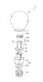
- FIG. 1is a side view of a light bulb shaped lamp 1 according to the present embodiment.
- FIG. 2is an exploded perspective view of the light bulb shaped lamp 1 according to the present embodiment.
- FIG. 3is a cross-sectional view of the light bulb shaped lamp 1 according to the present embodiment.
- the upper side of the drawingis the front (upper) of the bulb-shaped lamp 1
- the lower side of the drawingis the rear (lower) of the bulb-shaped lamp 1
- the left and right sides of the drawingare the sides of the bulb-shaped lamp 1. is there.
- “rearward”refers to the direction on the base side with respect to the substrate of the LED module
- “forward”refers to the direction opposite to the base relative to the substrate in the LED module.
- the “side”is a direction parallel to the main surface of the substrate of the LED module.
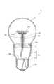
- the bulb-shaped lamp 1is a bulb-shaped LED lamp (LED bulb) which is a substitute for a bulb-shaped fluorescent lamp or an incandescent lamp.
- the light bulb-shaped lamp 1includes a translucent globe 10, LED modules 20a and 20b as light sources, a cap 30, which receives power from the outside of the lamp, a support 40, a support 50, a resin case 60, and lead wires. And a lighting circuit 80.
- an envelopeis configured by the glove 10, the resin case 60 (first case portion 61), and the base 30.
- the glove 10accommodates the LED modules 20a and 20b.
- the globe 10is made of a material transparent to the light from the LED modules 20a and 20b, and is a translucent globe that transmits the light from the LED modules 20a and 20b and transmits the light to the outside of the lamp.
- a glass bulbmade of silica glass that is transparent to visible light can be used.
- the LED modules 20 a and 20 b housed in the glove 10can be viewed from the outside of the glove 10.
- the shape of the glove 10is a shape in which one end is closed spherically and the other end has an opening 11. Specifically, the shape of the glove 10 is such that a part of the hollow sphere is narrowed while extending in a direction away from the center of the sphere, and the opening 11 is formed at a position away from the center of the sphere It is done.
- a glass bulb having the same shape as a general incandescent bulbcan be used.
- a glass bulbsuch as A-shaped, G-shaped or E-shaped can be used as the glove 10.
- the globe 10does not necessarily have to be transparent to visible light, and the globe 10 may have a light diffusing function.
- a milky white light diffusion filmmay be formed by applying a resin containing a light diffusion material such as silica or calcium carbonate, a white pigment, or the like on the entire inner surface or outer surface of the glove 10.
- the glove 10does not have to be made of silica glass.
- a glove 10 made of a resin material such as acrylicmay be used.
- the LED modules 20 a and 20 bare light emitting modules that have LEDs (LED chips) and emit light when power is supplied to the LEDs through the lead wires 70.
- the LED modules 20 a and 20 bare held in the hollow of the glove 10 by the columns 40.
- the LED modules 20a and 20bbe disposed at a central position of the spherical shape formed by the globe 10 (for example, inside the major part of the larger diameter of the globe 10).
- the light distribution characteristic of the light bulb shaped lamp 1becomes a light distribution characteristic similar to a general incandescent light bulb using a conventional filament coil. .
- the LED modules 20a and 20bare arranged such that the main surfaces (front and back surfaces) of the substrate intersect, for example, be substantially perpendicular to the lamp axis.
- the LED module 20 aemits light toward the front of the bulb-shaped lamp 1
- the LED module 20 bemits light toward the rear of the bulb-shaped lamp 1.
- the lamp axisis an axis serving as a rotation center when attaching the light bulb shaped lamp 1 to the socket of the lighting device (not shown), and coincides with the rotation axis of the base.
- the LED modules 20a and 20b configured in this wayare configured as one double-sided LED module that emits light from both sides.
- the detailed configuration of the LED modules 20a and 20bwill be described later.
- the base 30is a power receiving unit that receives power for causing the LEDs of the LED modules 20 a and 20 b to emit light from the outside of the light bulb shaped lamp 1.
- the base 30receives AC power at the two contacts, and the power received by the base 30 is input to the power input unit of the lighting circuit 80 through the lead wire.
- the base 30is attached to a socket of a lighting fixture (lighting device) and receives electric power from the socket to light the light bulb shaped lamp 1 (the LED modules 20a and 20b).
- the base 30is E-shaped, and a screwing portion for screwing with a socket of the lighting device is formed on the outer peripheral surface thereof, and a screwing portion for screwing with the resin case 60 is formed on the inner peripheral surface thereof. Is formed.
- the base 30is a bottomed cylindrical body made of metal.
- die etc.can be used as a screw-in type Edison type (E type
- a plug-in basemay be used as the base 30, a plug-in base may be used as the base 30, a plug-in base may be used.
- the support column 40is a stem provided to extend from the vicinity of the opening 11 of the glove 10 toward the inside of the glove 10 and functions as a holding member for holding the LED modules 20 a and 20 b in the glove 10.
- One end of the support 40is connected to the LED modules 20 a and 20 b, and the other end is connected to the support 50.
- the columns 40also function as a heat dissipation member for radiating the heat generated by the LED modules 20a and 20b to the base 30 side. Therefore, the heat dissipation efficiency of the support 40 can be enhanced by configuring the support 40 with a metal material having high thermal conductivity, such as aluminum having a thermal conductivity of 237 [W / m ⁇ K]. As a result, it is possible to suppress the decrease in the light emission efficiency and the life of the LED due to the temperature rise.
- the columns 40can also be made of resin or the like.
- the support column 40is configured by, for example, integrally molding the main shaft portion 41 and the fixing portion 42.
- the main shaft portion 41is a cylindrical member having a constant cross-sectional area.
- One end of the main shaft portion 41is connected to the fixing portion 42, and the other end is connected to the support 50.
- the fixing portion 42has a fixing surface to which the LED modules 20a and 20b are fixed, and this fixing surface is in contact with the back surface of the substrate of the LED modules 20a and 20b.
- the fixing portion 42further has a protrusion which protrudes from the fixing surface, and the protrusion fits with a through hole provided in the substrate of the LED modules 20a and 20b.
- the LED modules 20a and 20b and the fixing surfaceare adhered by an adhesive of resin such as silicone resin, for example.
- the support base (support plate) 50is a member for supporting the support column 40, and is fixed to the resin case 60.
- the support 50is connected to the open end of the opening 11 of the glove 10 and configured to close the opening 11 of the glove 10.
- the support 50is formed of a disk-like member having a step portion at the periphery, and the opening end of the opening 11 of the glove 10 is in contact with the step portion. In the step portion, the support 50, the resin case 60, and the open end of the opening 11 of the glove 10 are fixed by an adhesive.
- the support base 50is made of a metal material having a high thermal conductivity such as aluminum similarly to the support column 40, so that the heat dissipation efficiency of the heat of the LED modules 20a and 20b which thermally conducts the support column 50 by the support support 50 is enhanced. Be As a result, it is possible to further suppress the decrease in the light emission efficiency and the life of the LED due to the temperature rise.
- the resin case 60is an insulating case (circuit holder) for insulating the support 40 and the base 30 and housing the lighting circuit 80, and has a large diameter cylindrical first case portion 61 and a small diameter cylindrical second case. And a case portion 62.
- the resin case 60can be formed of, for example, polybutylene terephthalate (PBT).
- the second case portion 62is configured such that the outer circumferential surface is in contact with the inner circumferential surface of the mouthpiece 30, and a screwing portion for screwing with the mouthpiece 30 is formed on the outer circumferential surface of the second case portion 62. ing.
- the two lead wires 70are a pair of lead wires for supplying power for lighting the LED modules 20a and 20b from the lighting circuit 80 to the LED modules 20a and 20b, and are formed of a metal wire such as a copper wire. It can be configured.
- Each lead 70is disposed in the glove 10, one end is electrically connected to the external terminals of the LED modules 20a and 20b, and the other end is electrically connected to the power output portion of the lighting circuit 80, in other words, the cap 30 It is done.
- the lead wire 70also functions as a support for supporting the LED modules 20a and 20b by connecting a part of the lead 70 to the external terminals of the LED modules 20a and 20b.
- the two lead wires 70are, for example, vinyl wires composed of a metal core wire and an insulating resin covering the core wire, and the LED modules 20a and 20b are not covered with the insulating resin and the surface is exposed. It is electrically connected through the core wire which has been
- the lighting circuit 80is a circuit unit for lighting the LEDs of the LED modules 20a and 20b, and includes a plurality of circuit elements and a circuit board on which each circuit element is mounted.
- the lighting circuit 80includes a circuit for converting alternating current power supplied from the base 30 into direct current power, and supplies the converted direct current power to the LEDs of the LED modules 20a and 20b via the two lead wires 70. It is a drive circuit.
- the bulb-shaped lamp 1does not necessarily have to include the lighting circuit 80.
- the lighting circuit 80is not limited to the smoothing circuit, and the light control circuit, the booster circuit, and the like can be appropriately selected and combined.
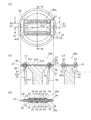
- FIG. 4is a view showing the configuration of the light bulb shaped lamp 1 according to the present embodiment.
- FIG. 5is an enlarged cross-sectional view of the LEDs in the LED modules 20a and 20b of the light bulb shaped lamp 1 according to the present embodiment.
- FIG. 4Ais a plan view when the LED module 20 a is viewed from above in a state where the globe 10 is removed in the light bulb shaped lamp 1.
- (b) of FIG. 4is a cross-sectional view of the same light bulb shaped lamp 1 cut along the AA 'line of (a), and
- (c) of FIG. 4is a BB' line of (a) 4
- (d)is a cross-sectional view of the same light bulb-shaped lamp 1 taken along the line CC 'of FIG. 4 (a).
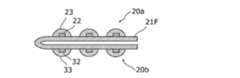
- the LED module 20 ais an example of a main light emitting module (first light emitting module), and has a COB (Chip On Board) structure in which a bare chip is directly mounted on the surface (one main surface) of the substrate 21.
- the LED module 20 bis an example of a sub light emitting module (second light emitting module), and has a COB structure in which a bare chip is directly mounted on the back surface (other main surface) of the substrate 21.
- the LED module 20 aincludes a substrate 21, a plurality of LEDs 22 provided on the surface of the substrate 21, a sealing member 23, metal wires 24 and 26, a wire 25, a conductive adhesive member 27 and a terminal (external terminal) 28.
- the LED module 20 bincludes the substrate 21, the plurality of LEDs 32 provided on the back surface of the substrate 21, the sealing member 33, the metal wires 34 and 36, the wires 35, the conductive adhesive members 37 and the terminals 38. There is.
- the substrate 21can be a light-transmitting substrate or a non-light-transmitting substrate.
- the substrate 21is, for example, a ceramic substrate made of a ceramic material such as aluminum oxide (alumina) or aluminum nitride, a metal substrate, a resin substrate, a glass substrate, a flexible substrate, an alumina substrate or the like.
- the substrate 21is preferably made of a white substrate such as a white alumina substrate having a low light transmittance with respect to light emitted from the LEDs 22 and 32, for example, 10% or less, or a metal substrate.
- the substrate 21has a light reflectance of 50% or more with respect to light emitted from the LEDs 22 and 32, and is made of a substrate containing Al 2 O 3 , MgO, SiO, or TiO 2 as a main component. be able to.
- the LED module 20aWhen the light transmittance of the substrate 21 is high, in the LED module 20a, a part of the light of the LED 22 on the front surface side of the substrate 21 passes through the substrate 21 and then passes further through the sealing member 33 on the back surface of the substrate 21 It is emitted from the back side of 21. Similarly, in the LED module 20b, after a part of the light of the LED 32 on the back surface side of the substrate 21 passes through the substrate 21, it further passes through the sealing member 23 on the surface of the substrate 21 and is emitted from the surface side of the substrate 21 . Therefore, in the light bulb shaped lamp 1, color shift occurs with respect to light extracted from the base side and the opposite side. On the other hand, such a color shift can be suppressed by lowering the light transmittance of the substrate 21. Further, since an inexpensive white substrate can be used, cost reduction of the light bulb shaped lamp 1 can be realized.
- two through holes 21 b penetrating from the front surface to the rear surface of the substrate 21are provided. These two through holes 21b constitute terminals 28 and 38 for connecting the lead wire 70 for feeding and the LED modules 20a and 20b, and the lead wire 70 is inserted through each of the two through holes 21b. .
- one through hole 21a penetrating from the front surface to the back surface of the substrate 21is provided.
- the through holes 21 aare for fixing the LED modules 20 a and 20 b to the support 40, and the projections 42 b of the support 40 are fitted in the through holes 21 a.
- the through hole 21amay not be provided.
- a plurality of LEDs 22are mounted on the surface of the substrate 21.
- the plurality of LEDs 22are arranged such that a plurality of element rows formed by being linearly arranged at the same pitch in the long side direction of the substrate 21 are arranged in the short side direction of the substrate 21.
- the plurality of LEDs 22are connected in series in the element row, and are connected in parallel in the element rows.
- This element rowis an example of the first light emitting element group.
- the distance (pitch) between adjacent LEDs 22 in an element rowis 1.8 mm
- the distance between the LEDs 22 of one element row and the LEDs 22 of the other element row in adjacent element rowsis 4 mm, for example It is arranged to be
- a plurality of LEDs 32are mounted on the back surface of the substrate 21.
- the plurality of LEDs 32are arranged such that a plurality of element rows formed by being linearly arranged at the same pitch in the long side direction of the substrate 21 are arranged in the short side direction of the substrate 21.
- the plurality of LEDs 32are connected in series in the element row, and are connected in parallel in the element rows. This element row is an example of the second light emitting element group.
- the LEDs 22 and 32are bare chips that emit monochromatic visible light in all directions, that is, sideways, upward and downward.
- the LEDs 22 and 32emit, for example, 20% of the total light amount laterally, 60% of the total light amount upward, and 20% of the total light amount downward.
- the LEDs 22 and 32are rectangular (square) blue LED chips that emit blue light when energized, for example, each side having a length of about 0.35 mm (350 ⁇ m).
- the blue LED chipfor example, a gallium nitride-based semiconductor light emitting device having a center wavelength of 440 nm to 470 nm, which is made of an InGaN-based material, can be used.
- the LEDs 22 and 32have a sapphire substrate 22a and a plurality of nitride semiconductor layers 22b stacked on the sapphire substrate 22a and having different compositions.
- a cathode electrode 22c and an anode electrode 22dare provided at both ends of the upper surface of the nitride semiconductor layer 22b.
- a wire bond portion 22eis provided on the cathode electrode 22c, and a wire bond portion 22f is provided on the anode electrode 22d.
- the cathode electrode 22c of one LED 22 and the anode electrode 22d of the other LED 22are connected by the wire 25 via the wire bond portions 22e and 22f.
- the LEDs 22 and 32are fixed on the substrate 21 by a translucent chip bonding material 22 g such that the surface on the sapphire substrate 22 a side faces the front surface or the back surface of the substrate 21.
- a translucent chip bonding material 22ga silicone resin containing a filler made of metal oxide can be used.
- the sealing member 23is a conversion member that converts the wavelength of light emitted by the LED 22, and is formed to cover the LED 22.
- the sealing member 23is a sealing resin composed of a wavelength conversion material for converting the wavelength of light emitted by the LED 22 and a resin material containing the wavelength conversion material.
- a wavelength conversion materialphosphor particles which are excited by the light emitted by the LED 22 and emit light of a desired color (wavelength) may be used, or light of a certain wavelength such as semiconductors, metal complexes, organic dyes and pigments
- a material containing a substance that absorbs light and emits light of a different wavelength from the absorbed lightcan also be used.
- a light diffusing materialsuch as silica particles may be dispersed.
- phosphor particleswhen the LED 22 is a blue LED chip that emits blue light, phosphor particles that wavelength-convert blue light to yellow light are used to emit white light from the sealing member 23 .
- YAG (yttrium aluminum garnet) -based yellow phosphor particlescan be used as the phosphor particles.
- part of the blue light emitted by the LED 22is wavelength-converted to yellow light by the yellow phosphor particles contained in the sealing member 23.
- the blue light which is not absorbed by the yellow phosphor particles (the wavelength is not converted) and the yellow light which is wavelength converted by the yellow phosphor particlesare diffused and mixed in the sealing member 23.
- the white lightis emitted from the sealing member 23.
- green phosphor particles, red phosphor particles, etc.may be used as the phosphor particles, and when the LED 22 is an LED 22 that emits ultraviolet light, as phosphor particles that are wavelength conversion materials A combination of phosphor particles emitting light of three primary colors (red, green and blue) is used.
- transparent resin materialssuch as silicone resin, organic materials such as fluorine resin, and inorganic materials such as low melting point glass and sol-gel glass can be used as the resin material containing the phosphor particles.
- the sealing member 23 configured as described aboveis formed in a straight line along the arrangement direction of the plurality of LEDs 22 constituting the element row, and collectively seals the element row of the LEDs 22. At the same time, a plurality of sealing members 23 are formed along the arrangement direction of the element rows to individually seal different element rows.
- Each sealing member 23has, for example, a length of 24 mm, a line width of 1.6 mm, and a central maximum height of 0.7 mm.
- the sealing member 33is a conversion member that converts the wavelength of light emitted by the LED 32, and is formed so as to cover the LED 32.
- the sealing member 33is a sealing resin composed of a wavelength conversion material for converting the wavelength of light emitted by the LED 32 and a resin material containing the wavelength conversion material.
- the wavelength conversion materialphosphor particles which are excited by the light emitted from the LED 32 and emit light of a desired color (wavelength) may be used, or light of a certain wavelength such as a semiconductor, metal complex, organic dye and pigment
- a material containing a substance that absorbs light and emits light of a different wavelength from the absorbed lightcan also be used.
- the sealing member 33is linearly formed along the arrangement direction of the plurality of LEDs 32 constituting the element row, and collectively seals the element rows of the LEDs 32. At the same time, a plurality of sealing members 33 are formed along the arrangement direction of the element rows to individually seal different element rows.
- Metal wiring, terminalIn order to electrically connect the element row of the LEDs 22 and the terminals 28 in parallel, two metal wires 26 are formed in the shape of islands in a predetermined shape at both ends of the substrate 21. These two metal wires 26 are formed on the surface of the substrate 21 so as to sandwich the element rows of the plurality of LEDs 22.
- the metal wiring 26protrudes toward the element row at a portion adjacent to the element row of the LED 22 on the surface of the substrate 21.
- the protruding portion of the metal wiring 26is a connection point with the wire 25 from the LED 22.
- two metal wirings 36are formed in the shape of islands in a predetermined shape at both ends of the substrate 21. These two metal wires 36 are formed on the back surface of the substrate 21 so as to sandwich the element rows of the plurality of LEDs 32.
- the metal wiring 36protrudes toward the element row at a portion adjacent to the element row of the LED 32 on the back surface of the substrate 21.
- the protruding portion of the metal wiring 36is a connection point with the wire 35 from the LED 32.
- the terminal 28is a feed electrode on which the conductive adhesive member 27 is provided, for example, a solder electrode to which soldering is performed, and the surface of the substrate 21 is surrounded by the through hole 21 b and the opening on the surface side of the substrate 21 of the through hole 21 b. And a land for connection formed in a predetermined shape.
- Two terminals 28are formed corresponding to each of the two metal wires 26.
- the pair of terminals 28is an example of a first terminal pair, is integrally formed with the corresponding metal wires 26, and is connected by being in contact with the corresponding metal wires 26.
- One corresponding wiring patternis configured by such a corresponding set of metal wires 26 and terminals 28.
- the terminal 28is a power supply unit of the LED module 20a, and receives power from the outside of the LED module 20a to emit light from the LED module 20, and supplies the received power to each LED 22 through the metal wires 26 and 24 and the wire 25. .
- the terminal 38is a feed electrode provided with the conductive adhesive member 37, and is formed in a predetermined shape on the back surface of the substrate 21 so as to surround the through hole 21b and the opening on the back surface side of the substrate 21 of the through hole 21b. And the land for connection.
- Two terminals 38are formed corresponding to each of the two metal wires 36.
- the pair of terminals 38is an example of a second terminal pair, is integrally formed with the corresponding metal wires 36, and is connected by being in contact with the corresponding metal wires 36.
- One corresponding wiring patternis configured by such a corresponding set of metal wires 36 and terminals 38.
- the terminal 38is a power supply unit of the LED module 20b, and receives power from the outside of the LED module 20b to emit light from the LED 32, and supplies the received power to each LED 32 through the metal wires 36 and 34 and the wire 35. .
- a plurality of metal wires 24are formed in a predetermined shape on the surface of the substrate 21 in order to electrically connect the plurality of LEDs 22 in series.
- the plurality of metal wires 24are formed in an island shape on the surface of the substrate 21 between the adjacent LEDs 22 in the element row.
- a plurality of metal wires 34are formed in a predetermined shape on the back surface of the substrate 21 in order to electrically connect the plurality of LEDs 32 in series.
- the plurality of metal wires 34are formed in an island shape between the adjacent LEDs 32 in the element row on the back surface of the substrate 21.
- the metal wires 26 and 24 and the terminals 28 of the above-described configurationare simultaneously patterned with the same metal material.
- a metal materialsilver (Ag), tungsten (W) or copper (Cu) etc. can be used, for example.
- the surfaces of the metal wires 26 and 24 and the terminals 28may be plated with nickel (Ni) / gold (Au) or the like.
- the metal wires 26 and 24 and the terminals 28may be made of different metal materials or may be formed in separate steps.
- metal lines 36 and 34 and terminal 38are simultaneously patterned with the same metal material.
- the wire 25is a wire for connecting the LED 22 and the metal wire 26 or the LED 22 and the metal wire 24 and is, for example, a gold wire. As described in FIG. 5, wire bonding of each of the wire bonding portions 22 e and 22 f provided on the upper surface of the LED 22 and the metal wiring 26 or the metal wiring 24 formed adjacent to both sides of the LED 22 by the wire 25 It is done.
- the wire 25is entirely embedded in the sealing member 23 so as not to be exposed from the sealing member 23, for example.
- the wire 35is an electric wire for connecting the LED 32 and the metal wire 36 or the LED 32 and the metal wire 34.
- wire bonding of the wire bonding portions 22 e and 22 f provided on the upper surface of the LED 32 and the metal wiring 36 or the metal wiring 34 formed adjacent to both sides of the LED 32 by the wire 35is wire bonding It is done.
- the wire 35is entirely embedded in the sealing member 33 so as not to be exposed from the sealing member 33, for example.
- the conductive adhesive member 27is a conductive adhesive such as solder or silver paste which connects the terminal 28 to the lead wire 70.
- the conductive adhesive member 27is provided in contact with both the terminal 28 and the lead wire 70 so as to cover the side surface of one end of the lead wire 70 on the surface of the terminal 28.
- the conductive adhesive member 27is provided to close the opening on the surface side of the substrate 21 of the through hole 21 b.
- the conductive adhesive member 37is a conductive adhesive that connects the terminal 38 to the lead 70.
- the conductive adhesive member 37is provided in contact with both the terminal 38 and the lead 70 so as to cover the side surface of one end of the lead 70 on the surface of the terminal 38.
- the conductive adhesive member 37is provided to close the opening on the back surface side of the substrate 21 of the through hole 21 b.
- the conductive adhesive members 27are used to form the two lead wires 70 and the terminals 38 after the members except the conductive adhesive members 27 and 37 are provided on the front and back surfaces of the substrate 21. It forms by connecting and connecting the two lead wires 70 and the terminal 28 by the conductive adhesive member 37.
- the lead wire 70is inserted from the opening on the back surface side of the through hole 21b and provided to protrude from the opening on the surface side of the through hole 21b.
- conductive adhesive member 37is provided to be in contact with both the back surface portion of lead wire 70 and terminal 38, and conductive adhesive member 27 is in contact with both the surface side portion and terminal 28.
- the terminal 28 and the terminal 38are connected by the lead wire 70. Then, the terminals 28 and 38 are connected to the same lead 70, and the plurality of LEDs 22 on the surface of the substrate 21 and the plurality of LEDs 32 on the back of the substrate 21 are connected in parallel to the lead 70.
- the current supplied to one positive lead wire 70passes through the conductive adhesive member 27, the terminal 28, the metal wiring 26, the LED 22 and the metal wiring 24, and the other minus It is outputted from the lead wire 70 on the side.
- the current supplied to the positive lead wire 70 on one sidepasses through the conductive adhesive member 37, the terminal 38, the metal wiring 36, the LED 32 and the metal wiring 34, and the other negative side It is output from the lead 70.
- the LED 32 and the sealing member 33Each member is not provided. Therefore, on the back surface of the substrate 21, the element rows of the plurality of LEDs 32 are provided to sandwich the fixing portion 42, and the distance between the element rows is the element row sandwiching the fixing portion 42 of the support column 40 than the distance between the other element rows. It is getting bigger. Further, in order to make the light emission characteristics of the LED modules 20a and 20b uniform, in the LED module 20a on the surface of the substrate 21, the elements of the plurality of LEDs 22 sandwich a portion located above the contact surface of the substrate 21 with the fixing portion 42. A row is provided. That is, the distance between the element rows of the LEDs 22 is larger than the distance between the other element rows in the element row sandwiching a portion located above the contact surface of the substrate 21 with the fixing portion 42.
- the conductive adhesive members 27 and 37are spaced apart from each other in the through hole 21b.
- the conductive adhesive members 27 and 37may not be separate members, but may be integrally provided as one adhesive member. That is, one conductive member may be provided continuously in the through hole 21b, on the surface of the substrate 21, and on the back surface of the substrate 21 so as to be in contact with the terminals 28 and 38 and the lead wire 70. .
- the tip of the lead wire 70is provided so as to be exposed on the surface of the conductive adhesive member 27, but may be completely covered by the conductive adhesive member 27. In this case, the contact area between the lead wire 70 and the conductive adhesive member 27 is increased, so that the connection between the both can be strengthened.
- the LED 22is located in the upper part of the contact surface with the fixing portion An element row of may be provided.
- the light bulb-shaped lamp 1 of the present embodimentis disposed in the glove 10, the pillar 40 provided so as to extend inward of the glove 10, and fixed to the pillar 40.
- LED modules 20a and 20bare provided.
- the light bulb shaped lamp 1further includes a lighting circuit 80 for supplying power to the LED modules 20a and 20b, and a pair of lead wires 70 for electrically connecting the LED modules 20a and 20b and the lighting circuit 80.
- the LED module 20 ais provided on the surface of the substrate 21 and the element row of the LEDs 22 provided on the surface of the substrate 21, and is a pair for electrically connecting the element row of the LEDs 22 and the lighting circuit 80. And a terminal 28.
- the LED module 20bis provided on the rear surface of the substrate 21 and on the rear surface of the substrate 21.
- the LED module 20bis provided on the rear surface of the substrate 21 and electrically connects the lighting array 80 with the device column of the LED 32. And a terminal 38.
- the LED module 20 a and the LED module 20 bare electrically connected in parallel via the pair of lead wires 70. That is, one double-sided light emission type LED module which emits light from both sides is configured by the LED module 20 a and the LED module 20 b connected in parallel.
- the pair of terminals 28are provided on the outer periphery of the two through holes 21 b provided on the substrate 21 and the two through holes 21 b on the surface of the substrate 21. It consists of lands.
- the pair of terminals 38is composed of two through holes 21 b and connection lands provided on the outer surface of the two through holes 21 b on the back surface of the substrate 21. Then, the pair of terminals 28 and the pair of terminals 38 are disposed so as to be approximately concentric, and the pair of lead wires 70 are inserted through the through holes 21 b. In other words, the terminal 28 and the terminal 38 are disposed so as to be approximately concentric, and the lead wire 70 is inserted into the through hole 21 b.
- the pair of lead wires 70is composed of a core wire and an insulating resin covering the core wire, and a portion of the pair of lead wires 70 protruding from the surface of the substrate 21 and a back surface of the substrate 21 only 3 mm or less
- the core wiremay not be covered with the insulating resin in the part.
- the element row of the LEDs 22 and the element row of the LEDs 32are each composed of a plurality of LEDs connected in series, and the element row of the LEDs 22 is the number of LEDs of the element row of the LEDs 32 Have the same number of LEDs.
- the pair of lead wires 70 and the pair of terminals 28 and the pair of terminals 38are electrically connected by the conductive adhesive member 27.
- the conductive adhesive member 27may be coated with an insulating resin.
- this insulating resinmay be white resin whose light transmittance is low with respect to the light emitted from LED22 and 32, for example, 10% or less.
- the surface of the support column 40has a light reflectance of 30% or more to the light emitted from the LED modules 20a and 20b.
- the pillars 40contain any of Al, Cu, and Fe as main components.
- the LED module 20 ahas an element row of a plurality of LEDs 22, and the LED module 20 b has an element row of a plurality of LEDs 32.
- the light bulb shaped lamp 1emits light from both sides of the substrate 21, light is taken out from the base side of the light bulb shaped lamp 1 and the opposite side thereof, and the light bulb shaped lamp 1 having a wide light distribution angle is realized. it can.
- power supply to the LED modules 20a and 20bis realized simply by connecting the lead wire 70 to both of the two terminals 28 and 38 by the conductive adhesive members 27 and 37 through the through holes 21b. Therefore, compared with the configuration in which the lead wire 70 is connected to either of the terminals 28 and 38 and the terminal 28 and the terminal 38 are connected by a via hole or the like, the configuration such as the via hole connecting the terminal 28 and the terminal 38 is unnecessary. It becomes. Further, the number of lead wires 70 can be halved as compared with the configuration in which the separate lead wires 70 are connected to the terminals 28 and 38. As a result, a light bulb shaped lamp 1 with a simple structure can be realized.
- the substrate 21has a light reflectance of 50% or more to the light emitted from the LED modules 20a and 20b. Then, the substrate 21 contains any of Al 2 O 3 , MgO, SiO, and TiO 2 as a main component. Thereby, the light transmittance of the substrate 21 can be lowered to suppress the color shift of the light emitted from the LED modules 20a and 20b. In addition, it is possible to reduce the cost of the light bulb shaped lamp 1 by using a low cost white substrate as the substrate 21.
- the back surface of the substrate 21is adhesively fixed to the support 40 so as to contact the support 40, and the LED modules 20a and 20b are directly fixed to the support 40. .
- the heat dissipation efficiency of the substrate 21can be enhanced. As a result, it is possible to suppress the decrease in the light emission efficiency and the life of the LEDs 22 and 32 due to the temperature rise.
- the bulb-type lamp 1 according to the present modificationis the above-described embodiment in that the substrate 21 of the LED module is configured by bonding the two substrates including the light source and the wiring for emitting light on the surface with an adhesive. It differs from the light bulb shaped lamp 1 in the form.
- points different from the light bulb shaped lamp 1 of the above embodimentwill be mainly described in detail.
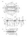
- FIG. 6is a view showing the configuration of the light bulb shaped lamp 1 according to the present modification.
- FIG. 6is a top view when the LED module 120a is seen from upper direction in the state except the globe 10 in the light bulb shaped lamp 1 which concerns on this modification.
- (b) of FIG. 6is a cross-sectional view of the same light bulb shaped lamp 1 cut along the AA 'line of (a)
- (c) of FIG. 6is a BB' line of (a) 6
- (d)is a cross-sectional view of the same light bulb-shaped lamp 1 taken along the line CC 'of FIG. 6 (a).
- the LED module 120 ais an example of a main light emitting module (first light emitting module), and has a COB structure in which a bare chip is directly mounted on the surface (one main surface) of the substrate 29.
- the LED module 120 bis an example of a sub light emitting module (second light emitting module), and has a COB structure in which a bare chip is directly mounted on the surface (one main surface) of the substrate 39.
- the LED module 120 aincludes a substrate 29, a plurality of LEDs 22 provided on the surface of the substrate 29, a sealing member 23, metal wires 24 and 26, a wire 25, a conductive adhesive member 27, and a terminal 28.
- the LED module 120 bincludes a substrate 39, a plurality of LEDs 32 provided on the surface of the substrate 39, a sealing member 33, metal wires 34 and 36, a wire 35, a conductive adhesive member 37 and terminals 38. There is.
- the substrate 29is an example of a main substrate, and the substrate 39 is an example of a sub substrate.
- the substrates 29 and 39have similar configurations and shapes, and the back surfaces of the substrates 29 and 39 are bonded to each other by an adhesive 90 to constitute one substrate 21.
- the substrates 29 and 39are, for example, a ceramic substrate such as aluminum nitride, a metal substrate, a resin substrate, a glass substrate, a flexible substrate, an alumina substrate or the like.
- the substrate 29is a rectangular mounting substrate for mounting the LED 22, and the substrate 39 is a rectangular mounting substrate for mounting the LED 32.
- the substrates 29 and 39are preferably made of a white substrate such as a white alumina substrate having a low light transmittance with respect to the light emitted from the LEDs 22 and 32, for example, 10% or less.
- the substrates 29 and 39have a light reflectance of 50% or more with respect to light emitted from the LEDs 22 and 32, and are substrates having any of Al 2 O 3 , MgO, SiO, and TiO 2 as main components. It can be configured. As a result, it is possible to reduce the light transmittance of the substrate 21 and to suppress the color shift of the light emitted from the LED modules 120a and 120b. In addition, it is possible to reduce the cost of the light bulb shaped lamp 1 by using a low cost white substrate for the substrates 29 and 39.
- the two through holes 29 b penetrating from the front surface to the back surface of the substrate 29are provided at both ends in the long side direction of the substrate 29, and both ends from the front surface to the back surface of the substrate 39 also There are two through holes 39b penetrating to the side.
- the through hole 29 bconstitutes a terminal 28 for connecting the lead wire 70 for feeding and the LED module 120 a
- the through hole 39 bis a terminal 38 for connecting the lead wire 70 for feeding and the LED module 120 b.
- the through holes 29 b and 39 bare arranged to be continuous to form the through hole 21 b of the substrate 21. Therefore, one lead 70 passes through one continuous through hole 29b and 39b.
- a central portion of the substrate 29is provided with one through hole 29a penetrating from the front surface to the rear surface of the substrate 29, and a central portion of the substrate 39 is a single penetration penetrating from the front surface to the rear surface of the substrate 39
- a hole 39ais provided.
- the through holes 29 a and 39 aare for fixing the LED modules 120 a and 120 b to the support column 40, and are arranged continuously to constitute one through hole 21 a of the substrate 21. Accordingly, the protrusions 42b of the support column 40 are fitted with the continuous through holes 29a and 39a.
- the adhesive 90is provided between the back surface of the substrate 29 and the back surface of the substrate 39 to bond the two, and is made of, for example, a resin such as silicone resin or a metal paste such as Ag paste.
- a resinsuch as silicone resin
- a metal pastesuch as Ag paste.
- the thermal conductivity between the substrate 29 and the substrate 39is enhanced to enhance the thermal conductivity as the substrate 21, so that the heat radiation efficiency of the substrate 21 can be enhanced.
- the light shielding property of the adhesive 90that is, the light shielding property of the substrate 21 can be enhanced, it is possible to suppress the color shift due to the light traveling from the front surface to the back surface of the substrates 29 and 39.
- Adhesive 90is at least a part of the space between through holes 29b and 39b between the back surface of substrate 29 and the back surface of substrate 39 so as not to prevent lead wire 70 from penetrating through holes 29b and 39b. Not provided. In addition, between the through holes 29a and 39a between the back surface of the substrate 29 and the back surface of the substrate 39, the adhesive 90 does not disturb the engagement of the through holes 29a and 39a with the protrusions of the support column 40. It is not provided in all of the space.
- the plurality of LEDs 22, the sealing member 23, the metal wires 24 and 26, the wires 25 and the terminals 28are provided on the surface of the substrate 29.
- a plurality of LEDs 32, sealing members 33, metal wires 34 and 36, wires 35 and terminals 38are provided on the surface of the substrate 39.
- the two lead wires 70 and the terminals 28are connected by the conductive adhesive member 27, and the two lead wires 70 and the terminals 38 by the conductive adhesive member 37. Is connected. Therefore, compared with the case where the light source and the wiring which makes this light-emit on both surfaces of the surface and back surface of one board
- the LED module 120 a and the LED module 120 bconstitute one double-sided LED module that emits light from both sides. Therefore, in the light bulb shaped lamp 1 of this modification, the light bulb shaped lamp 1 of a simple structure having a wide light distribution angle can be realized for the same reason as the light bulb shaped lamp 1 of the above embodiment.
- the substrate 21is composed of the substrate 29 on which the element row of the LEDs 22 is provided and the substrate 39 on which the element row of the LEDs 32 is provided.
- the substrates 29 and 39are disposed such that the element rows of the LEDs 22 and the back surfaces on which the element rows of the LEDs 32 are not provided face each other.
- the LED module 120 bmay be adhesively fixed to the support 40.
- the LED modules 120a and 120bcan be manufactured simply by preparing the separate substrates 29 and 39, providing the respective members individually on the respective surfaces, and bonding them, so that the LED modules 120a and 120b can be manufactured. Can be made easier. As a result, it is possible to realize the light bulb shaped lamp 1 which is easy to manufacture.
- the LED module 120 bis directly attached to the support 40, and the heat generated in the LED module 120 b is transferred to the support 40.
- the LED module 120ais indirectly attached to the support via the LED module 120b, and the heat generated in the LED module 120a is indirectly transferred to the support via the LED module 120b.
- an adhesive 90 as a heat conducting memberis provided between the LED modules 120a and 120b.
- the adhesive 90is any of a thermally conductive resin, a ceramic paste, and a metal paste.
- the heat radiation efficiency and the light shielding property of the substrate 21can be enhanced, it is possible to further suppress the decrease in the light emission efficiency and the life of the LEDs 22 and 32, and at the same time further suppress the color shift of the light emitted by the LED modules 120a and 120b. Can.
- the substrate 39has a through hole 39 c penetrating from the front surface to the back surface of the substrate 39, and the support 40 is a through hole 39 c of the substrate 39. And may be in contact with the back surface of the substrate 29. That is, the through hole 39 c may be formed to fit the entire fixing portion 42 of the support column 40, and the fixing surface of the fixing portion 42 of the support column 40 and the back surface of the substrate 29 may be bonded by the adhesive 90.
- the LED modules 120a and 120bcan be easily fixed to the support column 40, and the light bulb shaped lamp 1 can be realized which is easy to manufacture.
- the LED module 120ais adhesively fixed to the support 40 to shorten the heat radiation path from the substrate 29 to the support 40, and heat conduction such as grease is performed between the inner wall of the through hole 39b of the substrate 39 and the fixing portion 42 of the support 40.
- the heat radiation path from the substrate 39 to the support 40can be widened by making contact through the members. As a result, it is possible to further suppress the decrease in the light emission efficiency and the life of the LEDs 22 and 32.
- FIG. 7is a view showing another configuration of the light bulb shaped lamp 1 according to the present modification
- FIG. 7 (a)is a plan view when the LED module 120a is viewed from above with the glove 10 removed.
- (B) of FIG. 7is a cross-sectional view of the same light bulb shaped lamp 1 taken along the line AA 'of (a)
- (c) of FIG. 7is a BB' of (a)
- FIG. 7 (d)is a cross-sectional view of the same light bulb-shaped lamp 1 taken along the line CC ′ of FIG. 7 (a).
- the LEDis illustrated as a light emitting element in the above embodiment and modification, a semiconductor light emitting element such as a semiconductor laser, or an EL element such as organic EL (Electro Luminescence) or inorganic EL, or other solid light emitting element May be used.
- a semiconductor light emitting elementsuch as a semiconductor laser
- an EL elementsuch as organic EL (Electro Luminescence) or inorganic EL, or other solid light emitting element May be used.
- the LED moduleset it as the structure of the COB type which mounted the LED chip directly on the board
- a package type in which the LED chip is mounted in a recess (cavity) of a resin container and the phosphor-containing resin is enclosed in the recess, that is, a surface mount device (SMD) LED elementis used.
- SMDsurface mount device
- an LED module configured by mounting a plurality of the SMD type LED elements as a light emitting element on a substratemay be used.
- the supporthas a shape in which the width in the direction in which the LED element rows are arranged narrows in the direction from the support to the LED module.
- the supportmay have a shape in which the width in the arrangement direction of the LED element rows is expanded in the direction from the support to the LED module.
- FIG. 8Ais a plan view of the LED module 20 a as viewed from above with the globe 10 removed in the modification of the light bulb shaped lamp 1 according to the present embodiment.
- (b) of FIG. 8is a cross-sectional view of the same light bulb shaped lamp 1 cut along the AA 'line of (a), and (c) of FIG. 8 is a BB' line of (a) 4 is a cross-sectional view of the same bulb-shaped lamp 1 taken along the line.
- (d) of FIG. 8is a cross-sectional view of the same light bulb shaped lamp 1 cut along the C-C 'line of (a).
- the lead wireis provided outside the pillar, as shown in the sectional view of the light bulb shaped lamp in FIG. 9, a cavity is provided in the pillar and the lead wire A portion of may be provided in the support cavity.
- the lead wiredirectly enters the cavity in the support from the support base and then protrudes from the upper side of the support near the LED module and is connected to the LED module. Thereby, it can reduce that the light of a LED module is interrupted
- the lead wiresare provided to pierce the substrate from the back surface side of the substrate, but may be provided so as to pierce the lead wires from the front surface side of the substrate by turning the lead wires to the front surface side of the substrate.
- the LED 22 and the sealing member 23are provided on one surface of the flexible substrate 21F, and the flexible substrate 21F is bent so that the other surfaces are aligned with each other, thereby providing a dual emission type.
- the LED modulemay be configured.
- the double-sided light emitting type LED modulemay be configured by pasting together the LED module 20b having the SMD structure with the adhesive 90.
- the upper LED module 20ahas a COB structure and the lower LED module 20b has an SMD structure, but the upper LED module 20a has an SMD structure and the lower LED module 20b has a COB structure.
- the LED 22 and the sealing member 23may be provided on one surface of the substrate using one substrate, and the LED 22S may be provided on the other surface.
- a substrate 49X made of a material having a high light reflectance such as white aluminais embedded in a part of a light transmitting substrate 49Y made of a material having a high light transmittance such as light transmitting alumina or glass.
- a substrate 49 configured as described aboveis prepared, and the LED 22 and the sealing member 23 are formed on the surface of each of the substrate 49X and the substrate 49Y.
- the light from the LED 22 and the sealing member 23 provided on the surface of the translucent substrate 49Ytransmits the inside of the substrate 49X and is emitted from the opposite side (downward).
- the light from the LED 22 and the sealing member 23 provided on the surface of the substrate 49Xis not transmitted through the substrate 49X, is reflected by the substrate 49X, and travels upward.
- a light guide plate 59may be used to constitute a double-sided light emission type LED module.
- the LEDs 22Sare disposed to face the edge portions on both sides of the light guide plate 59.
- the light extraction efficiencymay be improved by, for example, forming a dot pattern on the surface of the light guide plate 59.
- the double-sided light emitting type LED moduleis fixed to the support column 40 so that light is mainly emitted upward and downward, as shown in FIGS. 11A and 11B.
- the double-sided light emitting type LED modulemay be fixed to the support 40 so that light is emitted mainly in the lateral direction. That is, the LED module may be erected on the support column 40 such that the main surface of the substrate in the double-sided light emission type LED module is substantially parallel to the lamp axis.
- the double-sided light emission type LED moduleas shown in FIG. 11A, the one used in the above embodiment (FIG. 1) may be used, or as shown in FIG. 11B, it is shown in FIG. You may use the thing of a structure.
- ones used in the other modified examples or ones having the configurations shown in FIGS. 10B to 10Dmay be used.
- a bulb-shaped lamp having a wide light distribution angleis realized by using a double-sided light emission type LED module that emits light from both sides, but a wide distribution can be achieved by the configuration shown in FIG.
- a light bulb-shaped lampmay be realized with a light angle.
- an LED and a sealing memberare provided on the upper surface (upper surface) of the substrate 21, and a reflective substrate with high reflectance such as a mirror is provided on the lower surface (lower surface) of the substrate 21. 69 is attached, and the LED 22S is disposed at a position below the reflective substrate 69 (for example, the support 50).
- the light emitted from the LED 22Scan be reflected by the reflective substrate 69 and travel to the base side.
- the light emitting unitthe LED 22 and the sealing member 23
- lightcan be extracted to the upper side and the lower side.
- a light bulb shaped lamp with a light anglecan be realized.
- this inventioncan also be implement
- a lighting device 100As shown in FIG. 13, as a lighting device 100 according to an embodiment of the present invention, a lighting device comprising the above-described bulb-shaped lamp 1 and a lighting fixture (lighting fixture) 200 to which the bulb-shaped lamp 1 is attached. It can be done.
- the lighting fixture 200turns off and lights the bulb-shaped lamp 1, and for example, the fixture body 210 attached to the ceiling and a translucent or non-translucent lamp cover covering the bulb-shaped lamp 1 And 220.
- the fixture body 210has a socket 211 to which the base of the bulb-shaped lamp 1 is attached and which supplies power to the bulb-shaped lamp 1.
- a translucent platemay be provided at the opening of the lamp cover 220.
- the present inventionis useful as a light bulb shaped lamp replacing conventional incandescent light bulbs and the like, and can be widely used in lighting devices and the like.
Landscapes
- Engineering & Computer Science (AREA)
- General Engineering & Computer Science (AREA)
- Physics & Mathematics (AREA)
- Microelectronics & Electronic Packaging (AREA)
- Optics & Photonics (AREA)
- Non-Portable Lighting Devices Or Systems Thereof (AREA)
- Led Device Packages (AREA)
Abstract
Description
Translated fromJapanese本発明は、電球形ランプ及び照明装置に関し、例えば、半導体発光素子を用いた電球形ランプ及びこれを用いた照明装置に関する。The present invention relates to a light bulb-shaped lamp and a lighting device, for example, to a light bulb-shaped lamp using a semiconductor light emitting element and a lighting device using the same.
近年、LED(Light Emitting Diode)等の半導体発光素子は、高効率及び長寿命であることから、各種ランプの新しい光源として期待されており、LEDを光源とするLEDランプの研究開発が進められている。In recent years, semiconductor light emitting devices such as LEDs (Light Emitting Diodes) are expected to be new light sources for various lamps due to their high efficiency and long life, and research and development of LED lamps using LEDs as light sources are underway There is.
このようなLEDランプとしては、電球形のLEDランプ(電球形LEDランプ)があり、電球形LEDランプでは、基板と、基板上に実装された複数のLEDとを備えるLEDモジュールが用いられる。例えば、特許文献1には、従来の電球形LEDランプが開示されている。As such an LED lamp, there is a bulb-shaped LED lamp (bulb-shaped LED lamp), and in the bulb-shaped LED lamp, an LED module including a substrate and a plurality of LEDs mounted on the substrate is used. For example,
ところで、従来の電球形LEDランプでは、LEDで発生する熱を放熱するためにヒートシンクが用いられており、LEDモジュールはこのヒートシンクに固定される。例えば、特許文献1に開示された電球形LEDランプでは、半球状のグローブと口金との間に、ヒートシンクとして機能する金属筐体が設けられ、LEDモジュールはこの金属筐体の上面に載置されている。By the way, in the conventional bulb-shaped LED lamp, a heat sink is used to dissipate heat generated by the LED, and the LED module is fixed to the heat sink. For example, in the light bulb-shaped LED lamp disclosed in
従って、このような従来の電球形LEDランプでは、LEDモジュールが発する光のうちヒートシンク側に放射される光は、金属製のヒートシンクによって遮られてしまうので、白熱電球又は電球形蛍光ランプ等の全配光特性を有するランプとは光の広がり方が異なる。つまり、従来の電球形LEDランプでは、白熱電球又は電球形蛍光ランプ等と同様の広い配光角を実現することが難しい。Therefore, in such a conventional bulb-shaped LED lamp, the light emitted to the heat sink side among the light emitted from the LED module is blocked by the metal heat sink, so that all light bulbs or bulb-shaped fluorescent lamps etc. The spread of light is different from a lamp having light distribution characteristics. That is, it is difficult for the conventional bulb-shaped LED lamp to realize the same wide light distribution angle as an incandescent bulb or a bulb-shaped fluorescent lamp.
そこで、電球形LEDランプにおいて、白熱電球と同様の構成を用いることが考えられる。つまり、ヒートシンクを用いずに、白熱電球のフィラメントコイルを単にLEDモジュールに置き換えた構成の電球形LEDランプが考えられる。この場合、LEDモジュールからの光は、ヒートシンクによって遮られない。Therefore, it is conceivable to use the same configuration as the incandescent bulb in the bulb-type LED lamp. That is, a bulb-shaped LED lamp having a configuration in which the filament coil of the incandescent bulb is simply replaced with the LED module without using a heat sink can be considered. In this case, the light from the LED module is not blocked by the heat sink.
しかしながら、電球形LEDランプに用いられるLEDモジュールは、通常、基板の片面(LEDが実装された面)のみから光を取り出すような構成となっている。従って、上述した置き換えの構成を用いたとしても、電球形LEDランプの口金側への光束は低く、広い配光角を実現することは困難である。これに対し、口金に向けて光を発する別のLEDモジュールを付加することで対応することもできるが、この場合には、2つのLEDモジュールに同時に給電を行うための構成が必要となり、電球形LEDランプとして構造が複雑化する。However, an LED module used for a bulb-type LED lamp is usually configured to extract light only from one side of the substrate (the side on which the LED is mounted). Therefore, even if the above-described replacement configuration is used, the luminous flux to the base of the bulb-type LED lamp is low, and it is difficult to realize a wide light distribution angle. On the other hand, this can be coped with by adding another LED module that emits light toward the base, but in this case, a configuration for simultaneously supplying power to two LED modules is required, and a light bulb is required. The structure becomes complicated as an LED lamp.
本発明は、このような問題を解決するためになされたものであり、広い配光角を持つ簡素な構造の電球形ランプ及び照明装置を提供することを目的とする。The present invention has been made to solve such problems, and it is an object of the present invention to provide a light bulb-shaped lamp and a lighting device with a simple structure having a wide light distribution angle.
上記課題を解決するために、本発明に係る電球形ランプの一態様は、透光性のグローブと、前記グローブの内方に向かって延びるように設けられた支柱と、前記グローブ内に配置され、前記支柱に固定された主発光モジュール及び副発光モジュールと、前記主発光モジュール及び前記副発光モジュールに電力を供給するための駆動回路と、前記主発光モジュール及び前記副発光モジュールと前記駆動回路とを電気的に接続するためのリード線対とを備え、前記主発光モジュールは、基板の表面上に設けられた第1発光素子群と、前記基板の表面上に設けられ、前記第1発光素子群と前記駆動回路とを電気的に接続するための第1端子対とを有し、前記副発光モジュールは、前記基板の裏面上に設けられた第2発光素子群と、前記基板の裏面上に設けられ、前記第2発光素子群と前記駆動回路とを電気的に接続するための第2端子対とを有し、前記主発光モジュールと前記副発光モジュールとが、前記リード線対を介して電気的に並列接続されていることを特徴とする。In order to solve the above problems, one aspect of the light bulb shaped lamp according to the present invention is disposed in a translucent glove, a post provided so as to extend inward of the glove, and the glove A main light emitting module and a sub light emitting module fixed to the support, a drive circuit for supplying power to the main light emitting module and the sub light emitting module, the main light emitting module, the sub light emitting module, and the drive circuit; A main light emitting module provided on the surface of the substrate, and the main light emitting module provided on the surface of the substrate; A second light emitting element group provided on the back surface of the substrate, and a second light emitting element group provided on the back surface of the substrate; And a second terminal pair for electrically connecting the second light emitting element group and the drive circuit, and the main light emitting module and the sub light emitting module are connected via the lead wire pair. And electrically connected in parallel.
さらに、本発明に係る電球形ランプの一態様において、前記基板は、前記第1発光素子群が表面に設けられた主基板と、前記第2発光素子群が表面に設けられた副基板とから構成され、前記主基板及び前記副基板が、前記第1発光素子群及び前記第2発光素子群を設けていない裏面同士が互いに対向するように配置されている、とすることができる。Furthermore, in one aspect of the light bulb shaped lamp according to the present invention, the substrate is a main substrate on which the first light emitting element group is provided on the surface, and a sub substrate on which the second light emitting element group is provided on the surface. The main substrate and the sub substrate may be arranged such that the back surfaces not provided with the first light emitting element group and the second light emitting element group face each other.
さらに、本発明に係る電球形ランプの一態様において、前記第1端子対が、前記基板に設けられた2つの貫通孔と、前記基板の表面における当該2つの貫通孔の外周に設けられた接続用ランドとから構成され、前記第2端子対が、前記2つの貫通孔と、前記基板の裏面における当該2つの貫通孔の外周に設けられた接続用ランドとから構成され、前記第1端子対及び前記第2端子対が、概略同心となるように配置され、前記リード線対が、前記貫通孔に挿通される、とすることができる。Furthermore, in one aspect of the light bulb shaped lamp according to the present invention, the first terminal pair is connected to two through holes provided in the substrate and the outer periphery of the two through holes on the surface of the substrate. And a land for connection, wherein the second terminal pair is comprised of the two through holes and a connection land provided on an outer periphery of the two through holes on the back surface of the substrate, the first terminal pair And the second pair of terminals may be disposed so as to be approximately concentric, and the pair of lead wires may be inserted into the through hole.
さらに、本発明に係る電球形ランプの一態様において、前記第1発光素子群及び前記第2発光素子群が、おのおの直列接続された複数の素子から構成され、前記第1発光素子群が、前記第2発光素子群の素子の数と同一の素子の数を有する、とすることができる。Furthermore, in one aspect of the light bulb shaped lamp according to the present invention, the first light emitting element group and the second light emitting element group are each configured of a plurality of elements connected in series, and the first light emitting element group is It is possible to have the same number of elements as the number of elements in the second light emitting element group.
さらに、本発明に係る電球形ランプの一態様において、前記リード線対と、前記第1端子対及び前記第2端子対とは、半田によって電気的に接続される、とすることができる。Furthermore, in one aspect of the light bulb shaped lamp according to the present invention, the lead wire pair may be electrically connected to the first terminal pair and the second terminal pair by solder.
さらに、本発明に係る電球形ランプの一態様において、前記半田が、絶縁性樹脂によって被覆されている、とすることができる。Furthermore, in one aspect of the light bulb shaped lamp according to the present invention, the solder may be covered with an insulating resin.
さらに、本発明に係る電球形ランプの一態様において、前記絶縁性樹脂が、白色である、とすることができる。Furthermore, in one aspect of the light bulb shaped lamp according to the present invention, the insulating resin can be white.
さらに、本発明に係る電球形ランプの一態様において、前記リード線対が、芯線と前記芯線を被覆する絶縁性樹脂とで構成され、前記リード線対における前記基板の裏面から3mm以下だけ突き出した部分では、前記芯線が前記絶縁性樹脂によって被覆されていない、とすることができる。Furthermore, in one aspect of the light bulb shaped lamp according to the present invention, the lead wire pair is composed of a core wire and an insulating resin covering the core wire, and protrudes by 3 mm or less from the back surface of the substrate in the lead wire pair. In the part, the core wire may not be covered with the insulating resin.
さらに、本発明に係る電球形ランプの一態様において、前記副発光モジュールが、前記支柱に直接的に取り付けられ、前記副発光モジュールで発生した熱を前記支柱に伝熱するとともに、前記主発光モジュールが、前記副発光モジュールを介して前記支柱に間接的に取り付けられ、前記主発光モジュールで発生した熱を、前記副発光モジュールを介して前記支柱に間接的に伝熱する、とすることができる。Furthermore, in one aspect of the light bulb shaped lamp according to the present invention, the sub light emitting module is directly attached to the support, and heat generated in the sub light emitting module is transferred to the support, and the main light emitting module May be indirectly attached to the support via the sub light emitting module, and the heat generated in the main light emitting module may be indirectly transferred to the support via the sub light emitting module. .
さらに、本発明に係る電球形ランプの一態様において、前記主発光モジュールと前記副発光モジュールとの間に、熱伝導部材が設けられている、とすることができる。Furthermore, in one aspect of the light bulb shaped lamp according to the present invention, a heat conducting member may be provided between the main light emitting module and the sub light emitting module.
さらに、本発明に係る電球形ランプの一態様において、前記熱伝導部材が、熱伝導性樹脂、セラミックペースト、及び金属ペーストのいずれかである、とすることができる。Furthermore, in one aspect of the light bulb shaped lamp according to the present invention, the heat conducting member can be any one of a heat conducting resin, a ceramic paste, and a metal paste.
さらに、本発明に係る電球形ランプの一態様において、前記副発光モジュールが、前記支柱に対し接着固定されている、とすることができる。Furthermore, in one aspect of the light bulb shaped lamp according to the present invention, the sub light emitting module can be adhesively fixed to the support.
さらに、本発明に係る電球形ランプの一態様において、前記基板が、前記第1発光素子群及び前記第2発光素子群から発せられる光に対して光反射率50%以上を有する、とすることができる。Furthermore, in one aspect of the light bulb shaped lamp according to the present invention, the substrate has a light reflectance of 50% or more with respect to light emitted from the first light emitting element group and the second light emitting element group. Can.
さらに、本発明に係る電球形ランプの一態様において、前記基板が、Al2O3、MgO、SiO、及びTiO2のいずれかを主成分とする、とすることができる。Furthermore, in one aspect of the light bulb shaped lamp according to the present invention, the substrate may contain any one of Al2 O3 , MgO, SiO and TiO2 as a main component.
さらに、本発明に係る電球形ランプの一態様において、前記支柱の表面が、前記主発光モジュール及び前記副発光モジュールから発せられる光に対して光反射率30%以上を有する、とすることができる。Furthermore, in one aspect of the light bulb shaped lamp according to the present invention, the surface of the support can have a light reflectance of 30% or more with respect to light emitted from the main light emitting module and the sub light emitting module. .
さらに、本発明に係る電球形ランプの一態様において、前記支柱が、Al、Cu、及びFeのいずれかを主成分とする、とすることができる。Furthermore, in one aspect of the light bulb shaped lamp according to the present invention, the support can be made mainly of any of Al, Cu and Fe.
さらに、本発明に係る電球形ランプの一態様において、前記主発光モジュールは、少なくとも2つ以上の前記第1発光素子群を有し、前記副発光モジュールは、少なくとも2つ以上の前記第2発光素子群を有する、とすることができる。Furthermore, in one aspect of the light bulb shaped lamp according to the present invention, the main light emitting module has at least two or more of the first light emitting element groups, and the sub light emitting module has at least two or more of the second light emitting It is possible to have an element group.
また、本発明に係る照明装置の一態様は、上記電球形ランプを備えることを特徴とする。Further, one aspect of a lighting device according to the present invention is characterized by including the above-described bulb-shaped lamp.
本発明によれば、広い配光角を持つ簡素な構造の電球形ランプ及び照明装置を実現することができる。According to the present invention, it is possible to realize a light bulb shaped lamp and a lighting device of a simple structure having a wide light distribution angle.
以下、本発明の実施の形態について、図面を用いて詳細に説明する。なお、以下で説明する実施の形態は、いずれも本発明の好ましい一具体例を示すものである。以下の実施の形態で示される数値、形状、材料、構成要素、構成要素の配置位置及び接続形態、ステップ、ステップの順序などは、一例であり、本発明を限定する主旨ではない。よって、以下の実施の形態における構成要素のうち、本発明の最上位概念を示す独立請求項に記載されていない構成要素については、本発明の課題を達成するのに必ずしも必要ではないが、より好ましい形態を構成するものとして説明される。また、図面において、実質的に同一の構成、動作、及び効果を表す要素については、同一の符号を付す。Hereinafter, embodiments of the present invention will be described in detail with reference to the drawings. The embodiments described below all show one preferable specific example of the present invention. Numerical values, shapes, materials, components, arrangement positions and connection forms of components, steps, order of steps, and the like shown in the following embodiments are merely examples, and the present invention is not limited thereto. Therefore, among the components in the following embodiments, components that are not described in the independent claim showing the highest concept of the present invention are not necessarily required to achieve the object of the present invention, It is described as constituting a preferred embodiment. Further, in the drawings, elements that represent substantially the same configuration, operation, and effect are denoted by the same reference numerals.
まず、本発明の実施の形態に係る電球形ランプ1の全体構成について、図1~図3を参照しながら説明する。First, the overall configuration of the light bulb shaped
図1は、本実施の形態に係る電球形ランプ1の側面図である。図2は、本実施の形態に係る電球形ランプ1の分解斜視図である。図3は、本実施の形態に係る電球形ランプ1の断面図である。FIG. 1 is a side view of a light bulb shaped
なお、図1~図3において、紙面上方が電球形ランプ1の前方(上方)であり、紙面下方が電球形ランプ1の後方(下方)であり、紙面左右が電球形ランプ1の側方である。ここで、本明細書において、「後方」とは、LEDモジュールの基板を基準として口金側の方向のことであり、「前方」とは、LEDモジュールの基板を基準として口金と反対側の方向のことであり、「側方」とは、LEDモジュールの基板の主面と平行な方向のことである。1 to 3, the upper side of the drawing is the front (upper) of the bulb-shaped
電球形ランプ1は、電球形蛍光灯又は白熱電球の代替品となる電球形LEDランプ(LED電球)である。電球形ランプ1は、透光性のグローブ10と、光源であるLEDモジュール20a及び20bと、ランプ外部から電力を受ける口金30と、支柱40と、支持台50と、樹脂ケース60と、リード線70と、点灯回路80とを備える。The bulb-shaped
電球形ランプ1は、グローブ10と樹脂ケース60(第1ケース部61)と口金30とによって外囲器が構成されている。In the light bulb shaped
[グローブ]
グローブ10は、LEDモジュール20a及び20bを収納する。グローブ10は、LEDモジュール20a及び20bからの光に対して透明な材料から構成され、LEDモジュール20a及び20bからの光を透過させてランプ外部に透光する透光性グローブである。このようなグローブ10としては、例えば可視光に対して透明なシリカガラス製のガラスバルブ(クリアバルブ)とすることができる。この場合、グローブ10内に収納されたLEDモジュール20a及び20bは、グローブ10の外側から視認することができる。[Globe]
The
グローブ10の形状は、一端が球状に閉塞され、他端に開口部11を有する形状である。具体的に、グローブ10の形状は、中空の球の一部が、球の中心部から遠ざかる方向に伸びながら狭まったような形状であり、球の中心部から遠ざかった位置に開口部11が形成されている。このような形状のグローブ10としては、一般的な白熱電球と同様の形状のガラスバルブを用いることができる。例えば、グローブ10として、A形、G形又はE形等のガラスバルブを用いることができる。The shape of the
なお、グローブ10は、必ずしも可視光に対して透明である必要はなく、グローブ10に光拡散機能を持たせてもよい。例えば、シリカや炭酸カルシウム等の光拡散材を含有する樹脂や白色顔料等をグローブ10の内面又は外面の全面に塗布することによって乳白色の光拡散膜を形成してもよい。また、グローブ10は、シリカガラス製である必要もない。例えば、アクリル等の樹脂材料によって作製されたグローブ10を用いても構わない。The
[LEDモジュール]
LEDモジュール20a及び20bは、LED(LEDチップ)を有し、リード線70を介してLEDに電力が供給されることにより発光する発光モジュールである。LEDモジュール20a及び20bは、支柱40によってグローブ10内の中空に保持されている。[LED module]
The
LEDモジュール20a及び20bは、グローブ10によって形成される球形状の中心位置(例えば、グローブ10の内径が大きい径大部分の内部)に配置されることが好ましい。このように、グローブ10の中心位置にLEDモジュール20a及び20bが配置されることにより、電球形ランプ1の配光特性は、従来のフィラメントコイルを用いた一般白熱電球と近似した配光特性となる。It is preferable that the
LEDモジュール20a及び20bは、その基板の主面(表面及び裏面)がランプ軸と交差、例えば略垂直となるように配置されている。そして、LEDモジュール20aは、電球形ランプ1の前方に向かって光を発し、LEDモジュール20bは、電球形ランプ1の後方に向かって光を発する。このとき、ランプ軸とは、電球形ランプ1を照明装置(不図示)のソケットに取り付ける際の回転中心となる軸であり、口金の回転軸と一致している。The
このように構成されるLEDモジュール20a及び20bは、両面から光を放出する両面発光型の1つのLEDモジュールとして構成される。なお、LEDモジュール20a及び20bの詳細な構成については後述する。The
[口金]
口金30は、LEDモジュール20a及び20bのLEDを発光させるための電力を電球形ランプ1外部から受ける受電部である。口金30は、二接点によって交流電力を受電し、口金30で受電した電力はリード線を介して点灯回路80の電力入力部に入力される。口金30は、照明器具(照明装置)のソケットに取り付けられてソケットから電力を受けることで電球形ランプ1(LEDモジュール20a及び20b)を点灯させる。[Cap]
The
例えば、口金30はE形であり、その外周面には照明装置のソケットに螺合させるための螺合部が形成され、その内周面には樹脂ケース60に螺合させるための螺合部が形成されている。口金30は、金属製の有底筒体形状である。なお、口金30としては、ねじ込み型のエジソンタイプ(E型)の口金として、E26形又はE17形の口金等を用いることができる。また、口金30として、差し込み型の口金を用いてもよい。For example, the
[支柱]
支柱40は、グローブ10の開口部11の近傍からグローブ10の内方に向かって延びるように設けられたステムであり、グローブ10内でLEDモジュール20a及び20bを保持する保持部材として機能する。支柱40の一端はLEDモジュール20a及び20bに接続され、他端は支持台50に接続されている。[Support]
The
支柱40は、LEDモジュール20a及び20bで発生する熱を口金30側に放熱させるための放熱部材としても機能する。従って、支柱40を熱伝導率の高い金属材料、例えば熱伝導率が237[W/m・K]のアルミニウム等により構成することで支柱40による放熱効率を高めることができる。その結果、温度上昇によるLEDの発光効率及び寿命の低下を抑制することができる。なお、支柱40は、樹脂等により構成することもできる。The
支柱40は、主軸部41と、固定部42とが例えば一体成型されて構成されている。主軸部41は、断面積が一定の円柱部材である。主軸部41の一端は固定部42に接続されており、他端は支持台50に接続されている。固定部42は、LEDモジュール20a及び20bが固定される固定面を有し、この固定面がLEDモジュール20a及び20bの基板の裏面と接する。固定部42は、さらに、固定面から突出する突起部を有し、この突起部はLEDモジュール20a及び20bの基板に設けられた貫通孔と嵌合する。LEDモジュール20a及び20bと固定面とは、例えばシリコーン樹脂等の樹脂の接着剤により接着される。The
[支持台]
支持台(支持板)50は、支柱40を支持する部材であり、樹脂ケース60に固定されている。支持台50は、グローブ10の開口部11の開口端に接続されてグローブ10の開口部11を塞ぐように構成されている。具体的に、支持台50は、周縁に段差部を有する円盤状部材で構成されており、その段差部にはグローブ10の開口部11の開口端が当接されている。そして、この段差部において、支持台50と樹脂ケース60とグローブ10の開口部11の開口端とは、接着剤によって固着されている。[Support stand]
The support base (support plate) 50 is a member for supporting the
支持台50は、支柱40と同様に、アルミニウム等の熱伝導率の高い金属材料により構成されることで、支持台50による支柱40を熱伝導したLEDモジュール20a及び20bの熱の放熱効率が高められる。その結果、温度上昇によるLEDの発光効率及び寿命の低下をさらに抑制することができる。The
[樹脂ケース]
樹脂ケース60は、支柱40と口金30とを絶縁すると共に点灯回路80を収納するための絶縁ケース(回路ホルダ)であり、大径円筒状の第1ケース部61と、小径円筒状の第2ケース部62とから構成されている。樹脂ケース60は、例えば、ポリブチレンテレフタレート(PBT)によって成形することができる。[Resin case]
The
第1ケース部61の外表面は外気に露出しているので、樹脂ケース60に伝導した熱は、主に第1ケース部61から放熱される。第2ケース部62は、外周面が口金30の内周面と接触するように構成されており、第2ケース部62の外周面には口金30と螺合するための螺合部が形成されている。Since the outer surface of the
[リード線]
2本のリード線70は、LEDモジュール20a及び20bを点灯させるための電力を点灯回路80からLEDモジュール20a及び20bに供給するためのリード線対であり、銅線等の針金状の金属電線より構成することができる。各リード線70は、グローブ10内に配置され、一端がLEDモジュール20a及び20bの外部端子と電気的に接続され、他端が点灯回路80の電力出力部、言い換えると口金30と電気的に接続されている。リード線70は、その一部がLEDモジュール20a及び20bの外部端子に接続されることでLEDモジュール20a及び20bを支持する支持部としても機能している。[Lead]
The two
2本のリード線70は、金属の芯線とこの芯線を被覆する絶縁性樹脂とで構成される例えばビニル線であり、LEDモジュール20a及び20bとは絶縁性樹脂で被覆されておらず表面がむき出しにされた芯線を介して電気的に接続される。The two
なお、リード線70のLEDモジュール20a及び20bとの接続関係の詳細については後述する。In addition, the detail of the connection relation with
[点灯回路]
点灯回路80は、LEDモジュール20a及び20bのLEDを点灯させるための回路ユニットであり、複数の回路素子と、各回路素子が実装される回路基板とを有する。点灯回路80は、口金30から給電された交流電力を直流電力に変換する回路を含み、2本のリード線70を介して変換後の直流電力をLEDモジュール20a及び20bのLEDに供給するための駆動回路である。[Lighting circuit]
The
なお、電球形ランプ1は、必ずしも点灯回路80を備える必要はない。例えば、照明器具又は電池等から電球形ランプ1に直接直流電力が供給される場合には、電球形ランプ1は、点灯回路80を備えなくてもよい。また、点灯回路80は、平滑回路に限られるものではなく、調光回路及び昇圧回路等も適宜選択して組み合わせて構成することができる。The bulb-shaped
次に、LEDモジュール20a及び20bの詳細な構成と、LEDモジュール20a及び20b並びにリード線70の接続関係とについて、図4及び図5を用いて説明する。Next, the detailed configuration of the
図4は、本実施の形態に係る電球形ランプ1の構成を示す図である。図5は、本実施の形態に係る電球形ランプ1のLEDモジュール20a及び20bにおけるLEDの拡大断面図である。FIG. 4 is a view showing the configuration of the light bulb shaped
なお、図4の(a)は電球形ランプ1においてグローブ10を除いた状態でLEDモジュール20aを上方から見たときの平面図である。そして、図4の(b)は(a)のA-A’線に沿って切断した同電球形ランプ1の断面図であり、図4の(c)は(a)のB-B’線に沿って切断した同電球形ランプ1の断面図であり、図4の(d)は(a)のC-C’線に沿って切断した同電球形ランプ1の断面図である。FIG. 4A is a plan view when the
LEDモジュール20aは、主発光モジュール(第1発光モジュール)の一例であり、ベアチップが直接基板21の表面(一方の主面)上に実装されたCOB(Chip On Board)構造である。一方、LEDモジュール20bは、副発光モジュール(第2発光モジュール)の一例であり、ベアチップが直接基板21の裏面(他方の主面)上に実装されたCOB構造である。The
LEDモジュール20aは、基板21と、基板21の表面上に設けられた複数のLED22、封止部材23、金属配線24及び26、ワイヤー25、導電性接着部材27並びに端子(外部端子)28とを備えている。一方、LEDモジュール20bは、基板21と、基板21の裏面上に設けられた複数のLED32、封止部材33、金属配線34及び36、ワイヤー35、導電性接着部材37並びに端子38とを備えている。The
[基板]
基板21は、透光性基板又は非透光性基板を用いることができる。基板21は、例えば酸化アルミニウム(アルミナ)又は窒化アルミニウム等のセラミック材料からなるセラミック基板、金属基板、樹脂基板、ガラス基板、フレキシブル基板又はアルミナ基板等である。基板21は、LED22及び32を実装するための矩形状の実装基板(LED実装用基板)である。基板21は、その長辺の長さをL1とし、短辺の長さをL2とし、厚みをdとすると、例えばL1=26mm、L2=13mm、d=1mmとされる。[substrate]
The
基板21は、LED22及び32から発せられる光に対して光透過率が低く例えば10%以下の白色アルミナ基板等の白色基板又は金属基板等で構成されることが好ましい。例えば、基板21は、LED22及び32から発せられる光に対して光反射率50%以上を有し、Al2O3、MgO、SiO、及びTiO2のいずれかを主成分とする基板で構成することができる。基板21の光透過率が高い場合、LEDモジュール20aにおいて、基板21の表面側のLED22の光の一部が基板21を通過した後、基板21の裏面の封止部材33をさらに通過して基板21の裏面側から発せられる。同様に、LEDモジュール20bにおいて、基板21の裏面側のLED32の光の一部が基板21を通過した後、基板21の表面の封止部材23をさらに通過して基板21の表面側から発せられる。従って、電球形ランプ1において、口金側及びそれと反対側から取り出される光について色ずれが発生する。これに対し、基板21の光透過率を低くすることでこのような色ずれを抑制することができる。また、安価な白色基板を用いることができるので、電球形ランプ1の低コスト化を実現できる。The
基板21の長辺方向の両端部には基板21の表面から裏面に向けて貫通する2つの貫通孔21bが設けられている。これら2つの貫通孔21bは給電用のリード線70とLEDモジュール20a及び20bとを接続するための端子28及び38を構成し、2つの貫通孔21bのそれぞれにはリード線70が挿通されている。At both ends in the long side direction of the
基板21の中央部には基板21の表面から裏面に向けて貫通する1つの貫通孔21aが設けられている。この貫通孔21aは、LEDモジュール20a及び20bを支柱40に固定するためのものであり、貫通孔21aには支柱40の突起部42bが嵌合されている。In the central portion of the
なお、貫通孔21aがなくても接着剤によりLEDモジュール20a及び20bの支柱40への固定は可能である。従って、貫通孔21aは設けられなくても構わない。In addition, even if there is no through-
[LED]
LED22は、基板21の表面の上に複数実装されている。複数のLED22は、基板21の長辺方向に同一ピッチで直線状に配列されて構成された素子列が基板21の短辺方向に複数本並べられるように配設されている。複数のLED22は素子列において直列接続され、素子列同士において並列接続されている。この素子列が第1発光素子群の一例である。例えば、複数のLED22は、素子列内において隣り合うLED22の間隔(ピッチ)が1.8mmとなり、隣り合う素子列において一方の素子列のLED22と他方の素子列のLED22との間隔が例えば4mmとなるように配設されている。[LED]
A plurality of
同様に、LED32は、基板21の裏面の上に複数実装されている。複数のLED32は、基板21の長辺方向に同一ピッチで直線状に配列されて構成された素子列が基板21の短辺方向に複数本並べられるように配設されている。複数のLED32は素子列において直列接続され、素子列同士において並列接続されている。この素子列が第2発光素子群の一例である。Similarly, a plurality of
LED22及び32は、全方位、つまり側方、上方及び下方に向けて単色の可視光を発するベアチップである。LED22及び32は、例えば、側方に全光量の20%、上方に全光量の60%、下方に全光量の20%の光を発する。The
LED22及び32は、例えば一辺の長さが約0.35mm(350μm)で、通電されることで青色光を発する矩形状(正方形)の青色LEDチップである。青色LEDチップとしては、例えばInGaN系の材料によって構成された、中心波長が440nm~470nmの窒化ガリウム系の半導体発光素子を用いることができる。The
LED22及び32は、図5に示すように、サファイア基板22aと、サファイア基板22a上に積層された、互いに異なる組成から構成される複数の窒化物半導体層22bとを有する。As shown in FIG. 5, the
窒化物半導体層22bの上面の両端部には、カソード電極22cとアノード電極22dとが設けられている。そして、カソード電極22cの上にはワイヤーボンド部22eが設けられ、アノード電極22dの上にはワイヤーボンド部22fが設けられている。例えば、隣り合うLED22において、一方のLED22のカソード電極22cと他方のLED22のアノード電極22dとは、ワイヤーボンド部22e及び22fを介して、ワイヤー25により接続されている。A
LED22及び32は、サファイア基板22a側の面が基板21の表面又は裏面と対向するように、透光性のチップボンディング材22gにより基板21の上に固定されている。チップボンディング材22gには、酸化金属から構成されるフィラーを含有したシリコーン樹脂等を用いることができる。チップボンディング材22gに透光性材料を使用することにより、LED22の側面から出る光の損失を低減することができ、チップボンディング材22gによる影の発生を抑制することができる。The
[封止部材]
封止部材23は、LED22が発する光の波長を変換する変換部材であり、LED22を覆うように形成されている。封止部材23は、LED22が発する光の波長を変換する波長変換材と、波長変換材を含有する樹脂材料とから構成される封止樹脂である。波長変換材としては、LED22が発する光によって励起されて所望の色(波長)の光を放出する蛍光体粒子を用いることもできるし、半導体、金属錯体、有機染料及び顔料等のある波長の光を吸収して吸収した光とは異なる波長の光を発する物質を含む材料を用いることもできる。なお、封止部材23には、シリカ粒子等の光拡散材が分散されていてもよい。[Sealing member]
The sealing
このような蛍光体粒子としては、LED22が青色光を発する青色LEDチップである場合、封止部材23から白色光を出射させるために、青色光を黄色光に波長変換する蛍光体粒子が用いられる。例えば、蛍光体粒子としてYAG(イットリウム・アルミニウム・ガーネット)系の黄色蛍光体粒子を用いることができる。これにより、LED22が発した青色光の一部は、封止部材23に含まれる黄色蛍光体粒子によって黄色光に波長変換される。そして、黄色蛍光体粒子に吸収されなかった(波長変換されなかった)青色光と、黄色蛍光体粒子によって波長変換された黄色光とは、封止部材23の中で拡散及び混合されることにより、封止部材23から白色光となって出射される。なお、蛍光体粒子として、黄色蛍光体粒子以外に緑色蛍光体粒子及び赤色蛍光体粒子等が用いられてもよく、LED22が紫外線を発するLED22である場合、波長変換材である蛍光体粒子としては、三原色(赤色、緑色、青色)に発光する各色蛍光体粒子を組み合わせたものが用いられる。As such phosphor particles, when the
一方、蛍光体粒子を含有させる樹脂材料としては、シリコーン樹脂等の透明樹脂材料、フッ素系樹脂等の有機材、並びに低融点ガラス及びゾルゲルガラス等の無機材等を用いることができる。On the other hand, transparent resin materials such as silicone resin, organic materials such as fluorine resin, and inorganic materials such as low melting point glass and sol-gel glass can be used as the resin material containing the phosphor particles.
上述した構成の封止部材23は、素子列を構成する複数のLED22の配列方向に沿って直線状に形成され、LED22の素子列を一括封止している。同時に、封止部材23は、素子列の配列方向に沿って複数形成され、異なる素子列を個別に封止している。1本あたりの封止部材23は、例えば、長さが24mm、線幅が1.6mm、中心最大高さが0.7mmである。The sealing
同様に、封止部材33は、LED32が発する光の波長を変換する変換部材であり、LED32を覆うように形成されている。封止部材33は、LED32が発する光の波長を変換する波長変換材と、波長変換材を含有する樹脂材料とから構成される封止樹脂である。波長変換材としては、LED32が発する光によって励起されて所望の色(波長)の光を放出する蛍光体粒子を用いることもできるし、半導体、金属錯体、有機染料及び顔料等のある波長の光を吸収して吸収した光とは異なる波長の光を発する物質を含む材料を用いることもできる。Similarly, the sealing
封止部材33は、素子列を構成する複数のLED32の配列方向に沿って直線状に形成され、LED32の素子列を一括封止している。同時に、封止部材33は、素子列の配列方向に沿って複数形成され、異なる素子列を個別に封止している。The sealing
[金属配線、端子]
金属配線26は、LED22の素子列と端子28とを電気的に並列接続するために、基板21の両端部に所定形状で島状に2つ形成されている。これら2つの金属配線26は、基板21の表面において、複数のLED22の素子列を挟み込むように形成されている。[Metal wiring, terminal]
In order to electrically connect the element row of the
金属配線26は、基板21の表面において、LED22の素子列と隣り合う部分で素子列に向かって突出している。この金属配線26の突出部は、LED22からのワイヤー25との接続箇所となる。The
同様に、金属配線36は、LED32の素子列と端子38とを電気的に並列接続するために、基板21の両端部に所定形状で島状に2つ形成されている。これら2つの金属配線36は、基板21の裏面において、複数のLED32の素子列を挟み込むように形成されている。Similarly, in order to electrically connect the element row of the
金属配線36は、基板21の裏面において、LED32の素子列と隣り合う部分で素子列に向かって突出している。この金属配線36の突出部は、LED32からのワイヤー35との接続箇所となる。The
端子28は、導電性接着部材27が設けられる給電電極、例えば半田付けが行われる半田電極であり、貫通孔21bと、貫通孔21bの基板21の表面側の開口を囲むように基板21の表面に所定形状で形成された接続用ランドとから構成されている。端子28は、2つの金属配線26のそれぞれに対応して2つ形成されている。この一対の端子28は、第1端子対の一例であり、それぞれ対応する金属配線26と一体化して形成され、対応する金属配線26と接することで接続されている。このような対応する1組の金属配線26及び端子28により1つの配線パターンが構成されている。The terminal 28 is a feed electrode on which the
端子28は、LEDモジュール20aの給電部であって、LED22を発光させるために、LEDモジュール20a外部から電力を受け、受けた電力を金属配線26及び24並びにワイヤー25を介して各LED22に供給する。The terminal 28 is a power supply unit of the
同様に、端子38は、導電性接着部材37が設けられる給電電極であり、貫通孔21bと、貫通孔21bの基板21の裏面側の開口を囲むように基板21の裏面に所定形状で形成された接続用ランドとから構成されている。端子38は、2つの金属配線36のそれぞれに対応して2つ形成されている。この一対の端子38は、第2端子対の一例であり、それぞれ対応する金属配線36と一体化して形成され、対応する金属配線36と接することで接続されている。このような対応する1組の金属配線36及び端子38により1つの配線パターンが構成されている。Similarly, the terminal 38 is a feed electrode provided with the
端子38は、LEDモジュール20bの給電部であって、LED32を発光させるために、LEDモジュール20b外部から電力を受け、受けた電力を金属配線36及び34並びにワイヤー35を介して各LED32に供給する。The terminal 38 is a power supply unit of the
金属配線24は、複数のLED22同士を電気的に直列接続するために、基板21の表面に所定形状で複数形成されている。これら複数の金属配線24は、基板21の表面において、素子列内で隣り合うLED22の間に島状に形成されている。A plurality of
同様に、金属配線34は、複数のLED32同士を電気的に直列接続するために、基板21の裏面に所定形状で複数形成されている。これら複数の金属配線34は、基板21の裏面において、素子列内で隣り合うLED32の間に島状に形成されている。Similarly, a plurality of
上述した構成の金属配線26及び24並びに端子28は同じ金属材料で同時にパターン形成される。金属材料としては、例えば、銀(Ag)、タングステン(W)又は銅(Cu)等を用いることができる。なお、金属配線26及び24並びに端子28の表面に、ニッケル(Ni)/金(Au)等のメッキ処理を施しても構わない。また、金属配線26及び24並びに端子28は、異なる金属材料により構成されてもよいし、別々の工程で形成されてもよい。The
同様に、金属配線36及び34並びに端子38は同じ金属材料で同時にパターン形成される。Similarly,
[ワイヤー]
ワイヤー25は、LED22と金属配線26、又はLED22と金属配線24とを接続するための電線であり、例えば、金ワイヤーである。図5で説明したように、このワイヤー25により、LED22の上面に設けられたワイヤーボンド部22e及び22fのそれぞれとLED22の両側に隣接して形成された金属配線26又は金属配線24とがワイヤボンディングされている。[wire]
The
ワイヤー25は、例えば、封止部材23から露出しないように、全体が封止部材23の中に埋め込まれる。The
同様に、ワイヤー35は、LED32と金属配線36、又はLED32と金属配線34とを接続するための電線である。図5で説明したように、このワイヤー35により、LED32の上面に設けられたワイヤーボンド部22e及び22fのそれぞれとLED32の両側に隣接して形成された金属配線36又は金属配線34とがワイヤボンディングされている。Similarly, the
ワイヤー35は、例えば、封止部材33から露出しないように、全体が封止部材33の中に埋め込まれる。The
[導電性部材]
導電性接着部材27は、端子28をリード線70と接続する半田又は銀ペースト等の導電性接着剤である。導電性接着部材27は、端子28の表面上でリード線70の一端の側面を被覆するように、端子28及びリード線70の両方に接して設けられている。導電性接着部材27は、貫通孔21bの基板21の表面側の開口を塞ぐように設けられている。[Conductive member]
The
同様に、導電性接着部材37は、端子38をリード線70と接続する導電性接着剤である。導電性接着部材37は、端子38の表面上でリード線70の一端の側面を被覆するように、端子38及びリード線70の両方に接して設けられている。導電性接着部材37は、貫通孔21bの基板21の裏面側の開口を塞ぐように設けられている。Similarly, the
図4のLEDモジュール20a及び20bは、導電性接着部材27及び37を除く各部材を基板21の表面及び裏面上に設けた後、導電性接着部材27により2つのリード線70と端子38とを接続し、導電性接着部材37により2つのリード線70と端子28とを接続することで形成される。このとき、リード線70と端子38との電気的な接続では、まず、リード線70が貫通孔21bの裏面側の開口から挿入されて貫通孔21bの表面側の開口から突き出るように設けられる。その後、そのリード線70の裏面側の部分と端子38との両方に接するように導電性接着部材37が設けられ、表面側の部分と端子28との両方に接するように導電性接着部材27が設けられる。従って、リード線70により端子28と端子38とが接続される。そして、同じリード線70に端子28及び38が接続されて、基板21表面の複数のLED22と、基板21裏面の複数のLED32とはリード線70に並列接続される。In the
また、図4のLEDモジュール20aでは、一方のプラス側のリード線70に供給された電流は、導電性接着部材27、端子28、金属配線26、LED22及び金属配線24を通過し、他方のマイナス側のリード線70から出力される。同様に、LEDモジュール20bでは、一方のプラス側のリード線70に供給された電流は、導電性接着部材37、端子38、金属配線36、LED32及び金属配線34を通過し、他方のマイナス側のリード線70から出力される。Further, in the
また、図4のLEDモジュール20bでは、基板21の裏面と支柱40の固定部42の固定面とを接触させるため、基板21の裏面の固定面と接する部分にはLED32及び封止部材33等の各部材が設けられていない。従って、基板21の裏面において、複数のLED32の素子列は固定部42を挟むように設けられており、素子列の間隔は支柱40の固定部42を挟む素子列で他の素子列の間隔より大きくなっている。また、LEDモジュール20a及び20bの発光特性を揃えるために、基板21の表面のLEDモジュール20aにおいて、基板21の固定部42との接触面の上方に位置する部分を挟むように複数のLED22の素子列が設けられている。つまり、LED22の素子列の間隔は基板21の固定部42との接触面の上方に位置する部分を挟む素子列で他の素子列の間隔より大きくなっている。Further, in the
なお、図4のLEDモジュール20a及び20bでは、導電性接着部材27及び37は貫通孔21b内の空間を隔てて離れて設けられるとした。しかし、複数のLED22及び32はリード線70に対して並列接続されるため、導電性接着部材27及び37は接していても特に問題はない。従って、導電性接着部材27及び37は別々の部材でなく、一体となって1つの接着部材として設けられても構わない。つまり、1つの導電性部材が、端子28及び38並びにリード線70と接するように、貫通孔21b内と、基板21の表面上と、基板21の裏面上とに連続して設けられてもよい。In the
また、図4のLEDモジュール20aでは、リード線70の先端が導電性接着部材27の表面で露出するように設けられるとしたが、導電性接着部材27により完全に被覆されていてもよい。この場合には、リード線70と導電性接着部材27との接触面積が増加するため、両者の接続を強固にすることができる。Further, in the
また、図4のLEDモジュール20a及び20bの発光特性を揃える必要のないときは、基板21の表面のLEDモジュール20aにおいて、基板21の固定部42との接触面の上方に位置する部分に、LED22の素子列を設けてもよい。In addition, when it is not necessary to make the light emission characteristics of the
以上のように本実施の形態の電球形ランプ1は、グローブ10と、グローブ10の内方に向かって延びるように設けられた支柱40と、グローブ10内に配置され、支柱40に固定されたLEDモジュール20a及び20bとを備える。電球形ランプ1は、さらに、LEDモジュール20a及び20bに電力を供給するための点灯回路80と、LEDモジュール20a及び20bと点灯回路80とを電気的に接続するための一対のリード線70を備える。そして、LEDモジュール20aは、基板21の表面上に設けられたLED22の素子列と、基板21の表面上に設けられ、LED22の素子列と点灯回路80とを電気的に接続するための一対の端子28とを有する。そして、LEDモジュール20bは、基板21の裏面上に設けられたLED32の素子列と、基板21の裏面上に設けられ、LED32の素子列と点灯回路80とを電気的に接続するための一対の端子38とを有する。そして、LEDモジュール20aとLEDモジュール20bとが、一対のリード線70を介して電気的に並列接続されている。つまり、並列接続されたLEDモジュール20aとLEDモジュール20bとによって、両面から光を放出する1つの両面発光型のLEDモジュールが構成されている。As described above, the light bulb-shaped
また、本実施の形態の電球形ランプ1では、一対の端子28が、基板21に設けられた2つの貫通孔21bと、基板21の表面における当該2つの貫通孔21bの外周に設けられた接続用ランドとから構成されている。そして、一対の端子38が、2つの貫通孔21bと、基板21の裏面における当該2つの貫通孔21bの外周に設けられた接続用ランドとから構成されている。そして、一対の端子28及び一対の端子38が、概略同心となるように配置され、一対のリード線70が、貫通孔21bに挿通されている。言い換えると、端子28及び端子38が、概略同心となるように配置され、リード線70が貫通孔21bに挿通されている。このとき、一対のリード線70が、芯線と芯線を被覆する絶縁性樹脂とで構成され、一対のリード線70における基板21の表面から突き出した部分と、基板21の裏面から3mm以下だけ突き出した部分とでは芯線が絶縁性樹脂によって被覆されていなくてもよい。Further, in the light bulb shaped
また、本実施の形態の電球形ランプ1では、LED22の素子列及びLED32の素子列が、おのおの直列接続された複数のLEDから構成され、LED22の素子列が、LED32の素子列のLEDの数と同一のLEDの数を有する。Further, in the light bulb shaped
また、本実施の形態の電球形ランプ1では、一対のリード線70と、一対の端子28及び一対の端子38とは、導電性接着部材27によって電気的に接続されている。このとき、導電性接着部材27は、絶縁性樹脂によって被覆されていてもよい。そして、この絶縁性樹脂が、LED22及び32から発せられる光に対して光透過率が低く例えば10%以下の白色樹脂であってもよい。Further, in the light bulb shaped
また、本実施の形態の電球形ランプ1では、支柱40の表面が、LEDモジュール20a及び20bから発せられる光に対して光反射率30%以上を有する。そして、支柱40が、Al、Cu、及びFeのいずれかを主成分とする。Further, in the light bulb shaped
また、本実施の形態の電球形ランプでは、LEDモジュール20aは、複数のLED22の素子列を有し、LEDモジュール20bは、複数のLED32の素子列を有する。Further, in the light bulb shaped lamp of the present embodiment, the
これにより、電球形ランプ1は基板21の両面から光を発するため、電球形ランプ1の口金側及びそれと反対側から光が取り出され、広い配光角を持つ電球形ランプ1を実現することができる。Thereby, since the light bulb shaped
また、LEDモジュール20a及び20bへの給電が、単に、リード線70を、貫通孔21bを通して導電性接着部材27及び37により2つの端子28及び38の両方と接続することで実現される。従って、端子28及び38のいずれかにリード線70を接続し、ビアホール等により端子28と端子38とを接続する構成と比較して、端子28と端子38とを接続するビアホール等の構成が不要となる。また、端子28及び38に別々のリード線70を接続する構成と比較してリード線70の数を半分にすることができる。その結果、簡素な構造の電球形ランプ1を実現することができる。Also, power supply to the
また、本実施の形態の電球形ランプ1では、基板21が、LEDモジュール20a及び20bから発せられる光に対して光反射率50%以上を有する。そして、基板21が、Al2O3、MgO、SiO、及びTiO2のいずれかを主成分とする。これにより、基板21の光透過率を低くしてLEDモジュール20a及び20bから発せられる光の色ずれを抑制することができる。また、基板21に低コストの白色基板を用いて電球形ランプ1を低コスト化することもできる。Further, in the light bulb shaped
また、本実施の形態の電球形ランプ1では、基板21の裏面は、支柱40と接するように支柱40に対し接着固定され、LEDモジュール20a及び20bが、支柱40に直接的に固定されている。これにより、基板21の放熱効率を高めることができる。その結果、温度上昇によるLED22及び32の発光効率及び寿命の低下を抑制することができる。Further, in the light bulb shaped
(変形例)
上記の実施の形態の電球形ランプ1は、1つの基板21の表面及び裏面の両面に光源及びこれを発光させる配線を設けることで、2つのLEDモジュール20a及び20bを形成し、電球形ランプ1の口金側及びそれと反対側に光を取り出すとした。しかしながら、2つの別々の基板の表面に個別に光源及びこれを発光させる配線を設け、2つの基板の裏面を張り合わせて1つの基板21とすることでも、電球形ランプ1の口金側及びそれと反対側に光を取り出すことができる。従って、本変形例に係る電球形ランプ1は、LEDモジュールの基板21がそれぞれ表面に光源及びこれを発光させる配線を備える2つの基板を接着剤で接着して構成される点で上記の実施の形態の電球形ランプ1と異なる。以下、上記の実施の形態の電球形ランプ1と異なる点を中心に詳述する。(Modification)
In the light bulb-shaped
図6は、本変形例に係る電球形ランプ1の構成を示す図である。FIG. 6 is a view showing the configuration of the light bulb shaped
なお、図6の(a)は本変形例に係る電球形ランプ1においてグローブ10を除いた状態でLEDモジュール120aを上方から見たときの平面図である。そして、図6の(b)は(a)のA-A’線に沿って切断した同電球形ランプ1の断面図であり、図6の(c)は(a)のB-B’線に沿って切断した同電球形ランプ1の断面図であり、図6の(d)は(a)のC-C’線に沿って切断した同電球形ランプ1の断面図である。In addition, (a) of FIG. 6 is a top view when the
LEDモジュール120aは、主発光モジュール(第1発光モジュール)の一例であり、ベアチップが直接基板29の表面(一方の主面)上に実装されたCOB構造である。一方、LEDモジュール120bは、副発光モジュール(第2発光モジュール)の一例であり、ベアチップが直接基板39の表面(一方の主面)上に実装されたCOB構造である。The
LEDモジュール120aは、基板29と、基板29の表面上に設けられた複数のLED22、封止部材23、金属配線24及び26、ワイヤー25、導電性接着部材27並びに端子28とを備えている。一方、LEDモジュール120bは、基板39と、基板39の表面上に設けられた複数のLED32、封止部材33、金属配線34及び36、ワイヤー35、導電性接着部材37並びに端子38とを備えている。The
なお、基板29は主基板の一例であり、基板39は副基板の一例である。The
[基板]
基板29及び39は、同様の構成及び形状を有し、接着剤90により互いの裏面が接着されて1つの基板21を構成している。基板29及び39は、例えば窒化アルミニウム等のセラミック基板、金属基板、樹脂基板、ガラス基板、フレキシブル基板又はアルミナ基板等である。基板29はLED22を実装するための矩形状の実装基板であり、基板39はLED32を実装するための矩形状の実装基板である。[substrate]
The
基板29及び39は、LED22及び32から発せられる光に対して光透過率が低く例えば10%以下の白色アルミナ基板等の白色基板で構成されることが好ましい。例えば、基板29及び39は、LED22及び32から発せられる光に対して光反射率50%以上を有し、Al2O3、MgO、SiO、及びTiO2のいずれかを主成分とする基板で構成することができる。これにより、基板21としての光透過率を低くしてLEDモジュール120a及び120bから発せられる光の色ずれを抑制することができる。また、基板29及び39に低コストの白色基板を用いて電球形ランプ1を低コスト化することができる。The
基板29の長辺方向の両端部には基板29の表面から裏面に向けて貫通する2つの貫通孔29bが設けられており、基板39の長辺方向の両端部にも基板39の表面から裏面に向けて貫通する2つの貫通孔39bが設けられている。貫通孔29bは、給電用のリード線70とLEDモジュール120aとを接続するための端子28を構成し、貫通孔39bは、給電用のリード線70とLEDモジュール120bとを接続するための端子38を構成している。貫通孔29b及び39bは、連続するように配置されて基板21の貫通孔21bを構成している。従って、1つのリード線70は、連続する1つの貫通孔29b及び39bを挿通している。The two through
基板29の中央部には基板29の表面から裏面に向けて貫通する1つの貫通孔29aが設けられており、基板39の中央部にも基板39の表面から裏面に向けて貫通する1つの貫通孔39aが設けられている。貫通孔29a及び39aは、LEDモジュール120a及び120bを支柱40に固定するためのものであり、連続するように配置されて基板21の1つの貫通孔21aを構成している。従って、支柱40の突起部42bは、連続する貫通孔29a及び39aと嵌合される。A central portion of the
[接着剤]
接着剤90は、基板29の裏面と基板39の裏面との間に設けられ、両者を接着するものであり、例えばシリコーン樹脂等の樹脂又はAgペースト等の金属ペースト等により構成されている。金属ペーストの場合、基板29と基板39との間での熱伝導率を高めて基板21としての熱伝導率が高められるので、基板21の放熱効率を高めることができる。その結果、温度上昇によるLED22及び32の発光効率及び寿命の低下を抑制することができる。また、接着剤90の遮光性つまり基板21の遮光性を高めることができるので、基板29及び39の表面から裏面に向かう光による色ずれも抑制することができる。[adhesive]
The adhesive 90 is provided between the back surface of the
接着剤90は、リード線70が貫通孔29b及び39bを挿通することを邪魔しないように、基板29の裏面と基板39の裏面との間における貫通孔29b及び39bの間の空間の少なくとも一部には設けられていない。また、接着剤90は、貫通孔29a及び39aと支柱40の突起部とが嵌合することを邪魔しないように、基板29の裏面と基板39の裏面との間における貫通孔29a及び39aの間の空間の全てにおいても設けられていない。
図6のLEDモジュール120a及び120bの製造では、まず、複数のLED22、封止部材23、金属配線24及び26、ワイヤー25並びに端子28が基板29の表面の上に設けられる。同様に、複数のLED32、封止部材33、金属配線34及び36、ワイヤー35並びに端子38が基板39の表面の上に設けられる。その後、基板29及び39が接着剤90により接着された後、導電性接着部材27により2つのリード線70と端子28とが接続され、導電性接着部材37により2つのリード線70と端子38とが接続される。従って、1つの基板29の表面及び裏面の両面に光源及びこれを発光させる配線を設ける場合と比較して、LEDモジュール120a及び120bの製造を容易にすることができる。In the manufacture of the
以上のように、本変形例では、LEDモジュール120aとLEDモジュール120bとによって、両面から光を放出する両面発光型の1つのLEDモジュールが構成されている。従って、本変形例の電球形ランプ1では、上記の実施の形態の電球形ランプ1と同様の理由により、広い配光角を持つ簡素な構造の電球形ランプ1を実現することができる。As described above, in the present modification, the
また、本変形例の電球形ランプ1では、基板21は、LED22の素子列が表面に設けられた基板29と、LED32の素子列が表面に設けられた基板39とから構成される。そして、基板29及び39が、LED22の素子列及びLED32の素子列を設けていない裏面同士が互いに対向するように配置されている。このとき、LEDモジュール120bが、支柱40に対し接着固定されていてもよい。これにより、別々の基板29及び39を用意して、それぞれの表面に個別に各部材を設けた後、それらを接着するだけでLEDモジュール120a及び120bを製造できるので、LEDモジュール120a及び120bの製造を容易にすることができる。その結果、製造が容易な電球形ランプ1を実現することができる。Further, in the light bulb shaped
また、本変形例の電球形ランプ1では、LEDモジュール120bが、支柱40に直接的に取り付けられ、LEDモジュール120bで発生した熱を支柱40に伝熱する。そしてLEDモジュール120aが、LEDモジュール120bを介して支柱40に間接的に取り付けられ、LEDモジュール120aで発生した熱を、LEDモジュール120bを介して支柱40に間接的に伝熱する。そして、LEDモジュール120a及び120bの間に、熱伝導部材としての接着剤90が設けられている。この接着剤90は、熱伝導性樹脂、セラミックペースト、及び金属ペーストのいずれかである。これにより、基板21の放熱効率及び遮光性を高めることができるので、LED22及び32の発光効率及び寿命の低下をさらに抑制し、同時にLEDモジュール120a及び120bが発する光の色ずれをさらに抑制することができる。Further, in the light bulb shaped
本変形例の電球形ランプ1では、図7に示されるように、基板39は、基板39の表面から裏面に向けて貫通する貫通孔39cを有し、支柱40は、基板39の貫通孔39cを突き抜けて基板29の裏面と接してもよい。つまり、貫通孔39cが支柱40の固定部42の全体と嵌合するように形成され、支柱40の固定部42の固定面と基板29の裏面とが接着剤90により接着されてもよい。これにより、LEDモジュール120a及び120bの支柱40への固定が容易になり、製造が容易な電球形ランプ1を実現することができる。また、LEDモジュール120aを支柱40に対し接着固定して基板29から支柱40への放熱経路を短くし、また基板39の貫通孔39bの内壁と支柱40の固定部42とをグリース等の熱伝導部材を介して接触させて基板39から支柱40への放熱経路を広くできる。その結果、LED22及び32の発光効率及び寿命の低下をさらに抑制することができる。In the light bulb shaped
なお、図7は本変形例に係る電球形ランプ1の他の構成を示す図であり、図7の(a)はグローブ10を除いた状態でLEDモジュール120aを上方から見たときの平面図であり、図7の(b)は(a)のA-A’線に沿って切断した同電球形ランプ1の断面図であり、図7の(c)は(a)のB-B’線に沿って切断した同電球形ランプ1の断面図であり、図7の(d)は(a)のC-C’線に沿って切断した同電球形ランプ1の断面図である。FIG. 7 is a view showing another configuration of the light bulb shaped
(その他の変形例)
以上、本発明に係る電球形ランプについて、実施の形態及び変形例に基づいて説明したが、本発明は、これらの実施の形態及び変形例に限定されるものではない。本発明の要旨を逸脱しない範囲内で当業者が思いつく各種変形を施したものも本発明の範囲内に含まれる。また、発明の趣旨を逸脱しない範囲で、実施の形態及び変形例における各構成要素を任意に組み合わせてもよい。(Other modifications)
As mentioned above, although the lightbulb-shaped lamp which concerns on this invention was demonstrated based on embodiment and a modification, this invention is not limited to these embodiment and a modification. It is within the scope of the present invention to apply various modifications that those skilled in the art would think within the scope of the present invention. In addition, each component in the embodiment and the modification may be arbitrarily combined without departing from the scope of the invention.
例えば、上記の実施の形態及び変形例において、発光素子としてLEDを例示したが、半導体レーザ等の半導体発光素子、又は、有機EL(Electro Luminescence)や無機EL等のEL素子、その他の固体発光素子を用いてもよい。For example, although the LED is illustrated as a light emitting element in the above embodiment and modification, a semiconductor light emitting element such as a semiconductor laser, or an EL element such as organic EL (Electro Luminescence) or inorganic EL, or other solid light emitting element May be used.
また、上記の実施の形態及び変形例において、LEDモジュールは基板上にLEDチップを直接実装したCOB型の構成としたが、これに限らない。例えば、樹脂製の容器の凹部(キャビティ)の中にLEDチップを実装して当該凹部内に蛍光体含有樹脂を封入したパッケージ型、つまり表面実装型(SMD:Surface Mount Device)のLED素子を用いて、このSMD型のLED素子を発光素子として基板上に複数個実装することで構成されたLEDモジュールを用いても構わない。Moreover, in said embodiment and modification, although the LED module set it as the structure of the COB type which mounted the LED chip directly on the board | substrate, it does not restrict to this. For example, a package type in which the LED chip is mounted in a recess (cavity) of a resin container and the phosphor-containing resin is enclosed in the recess, that is, a surface mount device (SMD) LED element is used. Alternatively, an LED module configured by mounting a plurality of the SMD type LED elements as a light emitting element on a substrate may be used.
また、上記の実施の形態及び変形例において、基板の表面及び裏面のそれぞれの上には複数の素子列が設けられるとしたが、1つの素子列だけが設けられてもよい。Further, in the above-described embodiment and modification, although a plurality of element rows are provided on each of the front and back surfaces of the substrate, only one element row may be provided.
また、上記の実施の形態及び変形例において、支柱は、支持台からLEDモジュールに向かう方向において、LEDの素子列の並び方向の幅が狭まる形状を有するとした。しかし、図8に示されるように、支柱は、支持台からLEDモジュールに向かう方向において、LEDの素子列の並び方向の幅が広がる形状を有してもよい。Further, in the above-described embodiment and modification, the support has a shape in which the width in the direction in which the LED element rows are arranged narrows in the direction from the support to the LED module. However, as illustrated in FIG. 8, the support may have a shape in which the width in the arrangement direction of the LED element rows is expanded in the direction from the support to the LED module.
なお、図8の(a)は本実施の形態に係る電球形ランプ1の変形例においてグローブ10を除いた状態でLEDモジュール20aを上方から見たときの平面図である。そして、図8の(b)は(a)のA-A’線に沿って切断した同電球形ランプ1の断面図であり、図8の(c)は(a)のB-B’線に沿って切断した同電球形ランプ1の断面図である。そして、図8の(d)は(a)のC-C’線に沿って切断した同電球形ランプ1の断面図である。FIG. 8A is a plan view of the
また、上記の実施の形態及び変形例において、リード線は支柱の外部に設けられるとしたが、図9の電球形ランプの断面図に示されるように、支柱内に空洞が設けられ、リード線の一部は支柱の空洞に設けられてもよい。この場合、リード線は、支持台から直接支柱内の空洞に入った後、LEDモジュールの近傍で支柱の上部側面から飛び出してLEDモジュールと接続される。これにより、LEDモジュールの光がリード線により遮光されるのを低減することができる。図9において、リード線は、基板の裏面側から基板に突き刺すように設けられているが、リード線を基板の表面側まで回り込ませて基板の表面側から突き刺すように設けられてもよい。In the above embodiment and modification, although the lead wire is provided outside the pillar, as shown in the sectional view of the light bulb shaped lamp in FIG. 9, a cavity is provided in the pillar and the lead wire A portion of may be provided in the support cavity. In this case, the lead wire directly enters the cavity in the support from the support base and then protrudes from the upper side of the support near the LED module and is connected to the LED module. Thereby, it can reduce that the light of a LED module is interrupted | blocked by the lead wire. In FIG. 9, the lead wires are provided to pierce the substrate from the back surface side of the substrate, but may be provided so as to pierce the lead wires from the front surface side of the substrate by turning the lead wires to the front surface side of the substrate.
また、上記の実施の形態及び変形例において、両面から光を放出する両面発光型のLEDモジュールとしては、図10A~図10Dに示す構成のものを用いることができる。Further, in the above embodiment and modification, as the double-sided light emitting type LED module which emits light from both sides, those having the configurations shown in FIGS. 10A to 10D can be used.
具体的には、図10Aに示すように、フレキシブル基板21Fの一方の面にLED22及び封止部材23を設けて、当該フレキシブル基板21Fを他方の面同士が合わせるように折り曲げることで、両面発光型のLEDモジュールを構成してもよい。Specifically, as shown in FIG. 10A, the
また、図10Bに示すように、基板29にLEDチップであるLED22及び封止部材23を形成してなるCOB型構造のLEDモジュール20aと、基板39にSMD型LED素子であるLED22Sを実装してなるSMD構造のLEDモジュール20bとを接着剤90で貼り合わせることによって、両面発光型のLEDモジュールを構成してもよい。なお、図10Bでは、上側のLEDモジュール20aをCOB構造とし、下側のLEDモジュール20bをSMD構造としているが、上側のLEDモジュール20aをSMD構造とし、下側のLEDモジュール20bをCOB構造としてもよい。また、2枚の基板を用いるのではなく、1枚の基板を用いて当該基板の一方の面にLED22及び封止部材23を設けて、他方の面にLED22Sを設けてもよい。Further, as shown in FIG. 10B, the
また、図10Cに示すように、基板49の一部を導光素材として、両面発光型のLEDモジュールを構成してもよい。具体的には、透光性アルミナやガラス等の光透過率が高い素材からなる透光性の基板49Yの一部に、白色アルミナ等の光反射率が高い素材からなる基板49Xを埋め込む等して構成された基板49を用意し、基板49X及び基板49Yのそれぞれの表面上にLED22及び封止部材23を形成する。これにより、透光性の基板49Yの表面上に設けられたLED22及び封止部材23からの光は、基板49Xの内部を透過して反対側(下方)から出射する。一方、基板49Xの表面上に設けられたLED22及び封止部材23からの光は、基板49Xを透過せずに基板49Xで反射して上方に向かう。Moreover, as shown to FIG. 10C, you may comprise a double-sided light emission type LED module by using a part of board |
また、図10Dに示すように、導光板59を用いて両面発光型のLEDモジュールを構成してもよい。具体的には、導光板59の両サイドのエッジ部分に対向するようにしてLED22Sを配置する。これにより、両側に位置するLED22Sから出射した光は、導光板59内を導光して導光板59の両主面(上面と下面)から外部に向かって出射する。なお、導光板59の表面にドットパターンを形成する等して、光取り出し効率を向上させるとよい。Further, as shown in FIG. 10D, a
また、上記の実施の形態及び変形例において、両面発光型のLEDモジュールは主に上方と下方とに光が出射するように支柱40に固定されていたが、図11A及び図11Bに示すように、両面発光型のLEDモジュールが主に横方向に光が出射するように支柱40に固定されていてもよい。つまり、両面発光型のLEDモジュールにおける基板の主面がランプ軸と略平行となるように、当該LEDモジュールを支柱40に立設してもよい。この場合、両面発光型のLEDモジュールとしては、図11Aに示すように、上記実施の形態(図1)で用いたものを使用してもよいし、図11Bに示すように、図10Aに示す構成のものを使用してもよい。また、これら以外に、その他の上記変形例で用いたもの、又は、図10B~図10Dに示す構成のものを使用してもよい。Further, in the above embodiment and modification, the double-sided light emitting type LED module is fixed to the
また、上記の実施形態及び変形例では、両面から光を放出する両面発光型のLEDモジュールを用いることで広い配光角を持つ電球形ランプを実現したが、図12に示す構成によって、広い配光角を持ち電球形ランプを実現してもよい。具体的には、図12に示すように、基板21の上方の面(上面)にLED及び封止部材を設けて、基板21の下方の面(下面)にミラー等の反射率の高い反射基板69を貼り付けて、反射基板69の下方の位置(例えば支持台50)にLED22Sを配置する。この構成によって、LED22Sから出射した光を、反射基板69で反射させて口金側へと進行させることができる。これにより、発光部(LED22、封止部材23)が基板21の上方の面(上面)にしか設けられていない場合であっても、上方と下方とに光を取り出すことができるので、広い配光角を持つ電球形ランプを実現することができる。Further, in the above embodiment and modification, a bulb-shaped lamp having a wide light distribution angle is realized by using a double-sided light emission type LED module that emits light from both sides, but a wide distribution can be achieved by the configuration shown in FIG. A light bulb-shaped lamp may be realized with a light angle. Specifically, as shown in FIG. 12, an LED and a sealing member are provided on the upper surface (upper surface) of the
また、本発明は、上記の電球形ランプを備える照明装置として実現することもできる。例えば、図13に示すように、本発明の実施の形態に係る照明装置100として、上記の電球形ランプ1と、当該電球形ランプ1が取り付けられる点灯器具(照明器具)200とを備える照明装置とすることができる。この場合、点灯器具200は、電球形ランプ1の消灯及び点灯を行うものであり、例えば、天井に取り付けられる器具本体210と、電球形ランプ1を覆う透光性又は非透光性のランプカバー220とを備える。このうち、器具本体210は、電球形ランプ1の口金が装着されるとともに電球形ランプ1に給電を行うソケット211を有する。なお、ランプカバー220の開口部に透光性プレートを設けてもよい。Moreover, this invention can also be implement | achieved as an illuminating device provided with said bulb-shaped lamp. For example, as shown in FIG. 13, as a
本発明は、従来の白熱電球等を代替する電球形ランプとして有用であり、照明装置等において広く利用することができる。INDUSTRIAL APPLICABILITY The present invention is useful as a light bulb shaped lamp replacing conventional incandescent light bulbs and the like, and can be widely used in lighting devices and the like.
1 電球形ランプ
10 グローブ
11 開口部
20a、20b、120a、120b LEDモジュール
21、29、39、49、49X、49Y 基板
21F フレキシブル基板
21a、21b、29a、29b、39a、39b、39c 貫通孔
22、22S、32 LED
22a サファイア基板
22b 窒化物半導体層
22c カソード電極
22d アノード電極
22e、22f ワイヤーボンド部
22g チップボンディング材
23、33 封止部材
24、26、34、36 金属配線
25、35 ワイヤー
27、37 導電性接着部材
28、38 端子
30 口金
40 支柱
41 主軸部
42 固定部
42b 突起部
50 支持台
59 導光板
60 樹脂ケース
61 第1ケース部
62 第2ケース部
69 反射基板
70 リード線
80 点灯回路
90 接着剤
100 照明装置
200 点灯器具
210 器具本体
211 ソケット
220 ランプカバー
Claims (18)
Translated fromJapanese前記グローブの内方に向かって延びるように設けられた支柱と、
前記グローブ内に配置され、前記支柱に固定された主発光モジュール及び副発光モジュールと、
前記主発光モジュール及び前記副発光モジュールに電力を供給するための駆動回路と、
前記主発光モジュール及び前記副発光モジュールと前記駆動回路とを電気的に接続するためのリード線対とを備え、
前記主発光モジュールは、
基板の表面上に設けられた第1発光素子群と、
前記基板の表面上に設けられ、前記第1発光素子群と前記駆動回路とを電気的に接続するための第1端子対とを有し、
前記副発光モジュールは、
前記基板の裏面上に設けられた第2発光素子群と、
前記基板の裏面上に設けられ、前記第2発光素子群と前記駆動回路とを電気的に接続するための第2端子対とを有し、
前記主発光モジュールと前記副発光モジュールとが、前記リード線対を介して電気的に並列接続されている
電球形ランプ。With a translucent glove,
A post provided to extend inward of the glove;
A main light emitting module and a sub light emitting module disposed in the glove and fixed to the support;
A driving circuit for supplying power to the main light emitting module and the sub light emitting module;
And a lead wire pair for electrically connecting the main light emitting module and the sub light emitting module to the drive circuit.
The main light emitting module is
A first light emitting element group provided on the surface of the substrate;
It has a first terminal pair provided on the surface of the substrate and electrically connecting the first light emitting element group and the drive circuit.
The sub light emitting module is
A second light emitting element group provided on the back surface of the substrate;
And a second terminal pair provided on the back surface of the substrate and electrically connecting the second light emitting element group to the drive circuit.
The bulb-shaped lamp, wherein the main light emitting module and the sub light emitting module are electrically connected in parallel via the lead wire pair.
前記主基板及び前記副基板が、前記第1発光素子群及び前記第2発光素子群を設けていない裏面同士が互いに対向するように配置されている
請求項1に記載の電球形ランプ。The substrate is composed of a main substrate on the surface of which the first light emitting element group is provided, and a sub substrate on which the second light emitting element group is provided on the surface of the substrate.
The light bulb shaped lamp according to claim 1, wherein the main substrate and the sub substrate are disposed such that the back surfaces not provided with the first light emitting element group and the second light emitting element group face each other.
前記第2端子対が、前記2つの貫通孔と、前記基板の裏面における当該2つの貫通孔の外周に設けられた接続用ランドとから構成され、
前記第1端子対及び前記第2端子対が、概略同心となるように配置され、
前記リード線対が、前記貫通孔に挿通される
請求項1または請求項2に記載の電球形ランプ。The first terminal pair is composed of two through holes provided in the substrate and connection lands provided on the outer periphery of the two through holes in the surface of the substrate.
The second terminal pair includes the two through holes and a connection land provided on an outer periphery of the two through holes on the back surface of the substrate.
The first terminal pair and the second terminal pair are arranged to be approximately concentric.
The light bulb shaped lamp according to claim 1, wherein the lead wire pair is inserted into the through hole.
前記第1発光素子群が、前記第2発光素子群の素子の数と同一の素子の数を有する
請求項3に記載の電球形ランプ。Each of the first light emitting element group and the second light emitting element group includes a plurality of elements connected in series;
The light bulb shaped lamp according to claim 3, wherein the first light emitting element group has the same number of elements as the number of elements of the second light emitting element group.
請求項3または請求項4に記載の電球形ランプ。The light bulb shaped lamp according to claim 3 or 4, wherein the lead wire pair, the first terminal pair and the second terminal pair are electrically connected by solder.
請求項5に記載の電球形ランプ。The light bulb shaped lamp according to claim 5, wherein the solder is covered with an insulating resin.
請求項6に記載の電球形ランプ。The light bulb shaped lamp according to claim 6, wherein the insulating resin is white.
前記リード線対における前記基板の裏面から3mm以下だけ突き出した部分では、前記芯線が前記絶縁性樹脂によって被覆されていない
請求項3に記載の電球形ランプ。The lead wire pair is composed of a core wire and an insulating resin covering the core wire,
The light bulb shaped lamp according to claim 3, wherein the core wire is not covered with the insulating resin in a portion of the lead wire pair which protrudes by 3 mm or less from the back surface of the substrate.
前記主発光モジュールが、前記副発光モジュールを介して前記支柱に間接的に取り付けられ、前記主発光モジュールで発生した熱を、前記副発光モジュールを介して前記支柱に間接的に伝熱する
請求項2に記載の電球形ランプ。The sub light emitting module is directly attached to the post, and transfers heat generated by the sub light emitting module to the post.
The main light emitting module is indirectly attached to the support via the sub light emitting module, and the heat generated in the main light emitting module is indirectly transferred to the support via the sub light emitting module. The light bulb shaped lamp according to 2.
請求項9に記載の電球形ランプ。The light bulb shaped lamp according to claim 9, wherein a heat conducting member is provided between the main light emitting module and the sub light emitting module.
請求項10に記載の電球形ランプ。The light bulb shaped lamp according to claim 10, wherein the heat conductive member is any one of a heat conductive resin, a ceramic paste, and a metal paste.
請求項9から請求項11のいずれか1項に記載の電球形ランプ。The light bulb shaped lamp according to any one of claims 9 to 11, wherein the sub light emitting module is adhesively fixed to the support pillar.
請求項1に記載の電球形ランプ。The light bulb shaped lamp according to claim 1, wherein the substrate has a light reflectance of 50% or more with respect to light emitted from the first light emitting element group and the second light emitting element group.
請求項13に記載の電球形ランプ。The light bulb shaped lamp according to claim 13, wherein the substrate contains any one of Al2 O3 , MgO, SiO, and TiO2 as a main component.
請求項1に記載の電球形ランプ。The light bulb shaped lamp according to claim 1, wherein a surface of the support has a light reflectance of 30% or more with respect to light emitted from the main light emitting module and the sub light emitting module.
請求項15に記載の電球形ランプ。The light bulb shaped lamp according to claim 15, wherein the post mainly contains any of Al, Cu and Fe.
前記副発光モジュールは、少なくとも2つ以上の前記第2発光素子群を有する
請求項1から請求項16のいずれか1項に記載の電球形ランプ。The main light emitting module has at least two or more of the first light emitting element groups,
The light bulb shaped lamp according to any one of claims 1 to 16, wherein the sub light emitting module has at least two or more of the second light emitting element groups.
照明装置。An illumination device comprising the light bulb shaped lamp according to any one of claims 1 to 17.
Priority Applications (1)
| Application Number | Priority Date | Filing Date | Title |
|---|---|---|---|
| JP2013542269AJPWO2014013671A1 (en) | 2012-07-17 | 2013-06-11 | Light bulb shaped lamp and lighting device |
Applications Claiming Priority (2)
| Application Number | Priority Date | Filing Date | Title |
|---|---|---|---|
| JP2012159059 | 2012-07-17 | ||
| JP2012-159059 | 2012-07-17 |
Publications (1)
| Publication Number | Publication Date |
|---|---|
| WO2014013671A1true WO2014013671A1 (en) | 2014-01-23 |
Family
ID=49948515
Family Applications (1)
| Application Number | Title | Priority Date | Filing Date |
|---|---|---|---|
| PCT/JP2013/003665WO2014013671A1 (en) | 2012-07-17 | 2013-06-11 | Bulb-type lamp and illumination device |
Country Status (2)
| Country | Link |
|---|---|
| JP (1) | JPWO2014013671A1 (en) |
| WO (1) | WO2014013671A1 (en) |
Cited By (3)
| Publication number | Priority date | Publication date | Assignee | Title |
|---|---|---|---|---|
| JP2015148730A (en)* | 2014-02-07 | 2015-08-20 | 日立アプライアンス株式会社 | Light diffusion member for LED illumination and LED illumination device using the same |
| WO2016165870A1 (en)* | 2015-04-15 | 2016-10-20 | Osram Gmbh | Luminous means having leds |
| WO2022207603A1 (en)* | 2021-04-01 | 2022-10-06 | Signify Holding B.V. | Optical and thermal improvement of a two-sided multi-channel filament |
Citations (6)
| Publication number | Priority date | Publication date | Assignee | Title |
|---|---|---|---|---|
| JP2002164580A (en)* | 2000-11-16 | 2002-06-07 | Jaenam Kim | Led lamp device |
| JP2010157459A (en)* | 2008-12-31 | 2010-07-15 | Keiji Iimura | Led lamp, and bulb-type led lamp |
| JP2010251775A (en)* | 2010-06-04 | 2010-11-04 | Sharp Corp | Light emitting device |
| JP2012069303A (en)* | 2010-09-21 | 2012-04-05 | Panasonic Corp | Lamp and lighting system |
| JP2012084394A (en)* | 2010-10-12 | 2012-04-26 | Panasonic Corp | Lamp |
| JP2012084274A (en)* | 2010-10-07 | 2012-04-26 | Toshiba Lighting & Technology Corp | Light-emitting device, light source body and lighting fixture |
- 2013
- 2013-06-11JPJP2013542269Apatent/JPWO2014013671A1/enactivePending
- 2013-06-11WOPCT/JP2013/003665patent/WO2014013671A1/enactiveApplication Filing
Patent Citations (6)
| Publication number | Priority date | Publication date | Assignee | Title |
|---|---|---|---|---|
| JP2002164580A (en)* | 2000-11-16 | 2002-06-07 | Jaenam Kim | Led lamp device |
| JP2010157459A (en)* | 2008-12-31 | 2010-07-15 | Keiji Iimura | Led lamp, and bulb-type led lamp |
| JP2010251775A (en)* | 2010-06-04 | 2010-11-04 | Sharp Corp | Light emitting device |
| JP2012069303A (en)* | 2010-09-21 | 2012-04-05 | Panasonic Corp | Lamp and lighting system |
| JP2012084274A (en)* | 2010-10-07 | 2012-04-26 | Toshiba Lighting & Technology Corp | Light-emitting device, light source body and lighting fixture |
| JP2012084394A (en)* | 2010-10-12 | 2012-04-26 | Panasonic Corp | Lamp |
Cited By (5)
| Publication number | Priority date | Publication date | Assignee | Title |
|---|---|---|---|---|
| JP2015148730A (en)* | 2014-02-07 | 2015-08-20 | 日立アプライアンス株式会社 | Light diffusion member for LED illumination and LED illumination device using the same |
| WO2016165870A1 (en)* | 2015-04-15 | 2016-10-20 | Osram Gmbh | Luminous means having leds |
| US10655791B2 (en) | 2015-04-15 | 2020-05-19 | Ledvance Gmbh | Luminous means having LEDs |
| WO2022207603A1 (en)* | 2021-04-01 | 2022-10-06 | Signify Holding B.V. | Optical and thermal improvement of a two-sided multi-channel filament |
| US12092271B2 (en) | 2021-04-01 | 2024-09-17 | Signify Holding B.V. | Optical and thermal improvement of a two-sided multi-channel filament |
Also Published As
| Publication number | Publication date |
|---|---|
| JPWO2014013671A1 (en) | 2016-06-30 |
Similar Documents
| Publication | Publication Date | Title |
|---|---|---|
| JP5830668B2 (en) | Light emitting device and light source for illumination | |
| JP5351365B1 (en) | Light emitting device and lamp | |
| WO2014013671A1 (en) | Bulb-type lamp and illumination device | |
| JP2014157691A (en) | Light emitting device and light source for lighting | |
| JP5681963B2 (en) | Light emitting device and lamp | |
| JP5838309B2 (en) | Light emitting device, illumination light source, and illumination device | |
| JP5420124B1 (en) | Light bulb shaped lamp, lighting device, and method of manufacturing light bulb shaped lamp | |
| JP6206789B2 (en) | Illumination light source and illumination device | |
| JP5948666B2 (en) | Illumination light source and illumination device | |
| JP5417556B1 (en) | Light bulb shaped lamp and lighting device | |
| JP5493058B1 (en) | Light bulb shaped lamp and lighting device | |
| WO2014030275A1 (en) | Light bulb-shaped lamp and lighting device | |
| WO2014030276A1 (en) | Bulb lamp and illumination device | |
| JP5465364B1 (en) | Light bulb shaped lamp and lighting device | |
| JP5563730B1 (en) | Illumination light source and illumination device | |
| JP5793721B2 (en) | Illumination light source and illumination device | |
| JP5433818B1 (en) | Light bulb shaped lamp and lighting device | |
| CN204372573U (en) | Bulb-shaped lamp and lighting device | |
| WO2014041721A1 (en) | Light source for illumination and illumination device | |
| JP2014146510A (en) | Light source for lighting and lighting device |
Legal Events
| Date | Code | Title | Description |
|---|---|---|---|
| ENP | Entry into the national phase | Ref document number:2013542269 Country of ref document:JP Kind code of ref document:A | |
| 121 | Ep: the epo has been informed by wipo that ep was designated in this application | Ref document number:13819194 Country of ref document:EP Kind code of ref document:A1 | |
| NENP | Non-entry into the national phase | Ref country code:DE | |
| 122 | Ep: pct application non-entry in european phase | Ref document number:13819194 Country of ref document:EP Kind code of ref document:A1 |