WO2013187046A1 - Thin film transistor - Google Patents
Thin film transistorDownload PDFInfo
- Publication number
- WO2013187046A1 WO2013187046A1PCT/JP2013/003648JP2013003648WWO2013187046A1WO 2013187046 A1WO2013187046 A1WO 2013187046A1JP 2013003648 WJP2013003648 WJP 2013003648WWO 2013187046 A1WO2013187046 A1WO 2013187046A1
- Authority
- WO
- WIPO (PCT)
- Prior art keywords
- film
- layer
- thin film
- oxide semiconductor
- cumn alloy
- Prior art date
Links
Images


Classifications
- H—ELECTRICITY
- H10—SEMICONDUCTOR DEVICES; ELECTRIC SOLID-STATE DEVICES NOT OTHERWISE PROVIDED FOR
- H10D—INORGANIC ELECTRIC SEMICONDUCTOR DEVICES
- H10D62/00—Semiconductor bodies, or regions thereof, of devices having potential barriers
- H10D62/80—Semiconductor bodies, or regions thereof, of devices having potential barriers characterised by the materials
- H10D62/85—Semiconductor bodies, or regions thereof, of devices having potential barriers characterised by the materials being Group III-V materials, e.g. GaAs
- H—ELECTRICITY
- H10—SEMICONDUCTOR DEVICES; ELECTRIC SOLID-STATE DEVICES NOT OTHERWISE PROVIDED FOR
- H10D—INORGANIC ELECTRIC SEMICONDUCTOR DEVICES
- H10D30/00—Field-effect transistors [FET]
- H10D30/60—Insulated-gate field-effect transistors [IGFET]
- H10D30/67—Thin-film transistors [TFT]
- H10D30/6729—Thin-film transistors [TFT] characterised by the electrodes
- H10D30/6737—Thin-film transistors [TFT] characterised by the electrodes characterised by the electrode materials
- H10D30/6739—Conductor-insulator-semiconductor electrodes
- H—ELECTRICITY
- H10—SEMICONDUCTOR DEVICES; ELECTRIC SOLID-STATE DEVICES NOT OTHERWISE PROVIDED FOR
- H10D—INORGANIC ELECTRIC SEMICONDUCTOR DEVICES
- H10D30/00—Field-effect transistors [FET]
- H10D30/60—Insulated-gate field-effect transistors [IGFET]
- H10D30/67—Thin-film transistors [TFT]
- H10D30/674—Thin-film transistors [TFT] characterised by the active materials
- H10D30/6755—Oxide semiconductors, e.g. zinc oxide, copper aluminium oxide or cadmium stannate
- H—ELECTRICITY
- H10—SEMICONDUCTOR DEVICES; ELECTRIC SOLID-STATE DEVICES NOT OTHERWISE PROVIDED FOR
- H10D—INORGANIC ELECTRIC SEMICONDUCTOR DEVICES
- H10D64/00—Electrodes of devices having potential barriers
- H10D64/60—Electrodes characterised by their materials
- H10D64/62—Electrodes ohmically coupled to a semiconductor
- H—ELECTRICITY
- H10—SEMICONDUCTOR DEVICES; ELECTRIC SOLID-STATE DEVICES NOT OTHERWISE PROVIDED FOR
- H10K—ORGANIC ELECTRIC SOLID-STATE DEVICES
- H10K59/00—Integrated devices, or assemblies of multiple devices, comprising at least one organic light-emitting element covered by group H10K50/00
- H10K59/10—OLED displays
- H10K59/12—Active-matrix OLED [AMOLED] displays
Definitions
- the technology disclosed hereinrelates to a thin film transistor used in a liquid crystal display device, an organic EL (Electro-Luminescence) display device, and the like, an organic EL display device using the thin film transistor, and a method of manufacturing the thin film transistor.
- a thin film transistorused in a liquid crystal display device, an organic EL (Electro-Luminescence) display device, and the like
- an organic EL display device using the thin film transistorand a method of manufacturing the thin film transistor.
- TFTthin film transistor
- the configuration of the thin film transistorincludes a bottom gate type thin film transistor having a structure in which a gate electrode is formed below the channel layer (substrate side), or a top gate type having a structure in which the gate electrode is formed above the channel layer.
- a thin film transistorFor example, a silicon semiconductor or an oxide semiconductor is used for the channel layer of the thin film transistor.
- the bottom gate type thin film transistorincludes a channel etching structure in which the channel layer is etched and a channel etching in which a channel etching stopper is formed to suppress damage to the channel layer when forming the source electrode and the drain electrode.
- a channel etching stopperis formed to suppress damage to the channel layer when forming the source electrode and the drain electrode.
- Patent Document 1discloses a thin film transistor having a channel etching stopper structure in which a channel layer is an oxide semiconductor.
- a channel etching stopperfor example, a SiO 2 thin film is used in order to prevent the oxide semiconductor from changing its characteristics due to the reducing gas when the channel etching stopper is formed.
- the technique disclosed hereinis intended to obtain desired transistor characteristics.
- One embodiment of a thin film transistor that solves the above problemis formed between a gate electrode formed above a substrate, an oxide semiconductor layer formed above the substrate, and the gate electrode and the oxide semiconductor layer.
- Each of the plurality of electrodesincludes a Mo film, a Cu film, and a CuMn alloy film. Or a laminated film in which a CuMn alloy film, a Cu film, and a CuMn alloy film are laminated in this order from the bottom to the top.
- FIG. 1is a partially cutaway perspective view of an organic EL display device according to an embodiment.
- FIG. 2is a perspective view illustrating an example of a pixel bank of the organic EL display device according to the embodiment.
- FIG. 3is an electric circuit diagram showing a configuration of a pixel circuit in the organic EL display device according to the embodiment.
- FIG. 4is a schematic cross-sectional view of the thin film transistor according to the embodiment.
- FIG. 5Ais a cross-sectional view of the gate electrode formation step in the method for manufacturing the thin film transistor according to the embodiment.
- FIG. 5Bis a cross-sectional view of the gate insulating film forming step in the method for manufacturing the thin film transistor according to the embodiment.
- FIG. 5Cis a cross-sectional view of the oxide semiconductor layer formation step in the method for manufacturing the thin film transistor according to the embodiment.
- FIG. 5Dis a cross-sectional view of the oxide semiconductor layer processing resist pattern forming step in the method of manufacturing a thin film transistor according to the embodiment.
- FIG. 5Eis a cross-sectional view of the oxide semiconductor layer processing step in the method for manufacturing the thin film transistor according to the embodiment.
- FIG. 5Fis a cross-sectional view of the oxide semiconductor layer processing resist pattern removal step in the method of manufacturing a thin film transistor according to the embodiment.
- FIG. 5Gis a cross-sectional view of a stacked film forming step of a source electrode and a drain electrode in the thin film transistor manufacturing method according to the embodiment.
- FIG. 5His a cross-sectional view of a resist electrode forming process for processing a source electrode and a drain electrode in the thin film transistor manufacturing method according to the embodiment.
- FIG. 5Iis a cross-sectional view of the source electrode and drain electrode processing step in the method of manufacturing a thin film transistor according to the embodiment.
- FIG. 5Jis a cross-sectional view of a resist pattern removal process for processing a source electrode and a drain electrode in the method for manufacturing a thin film transistor according to the embodiment.
- FIG. 5Kis a cross-sectional view of a protective film forming step in the method of manufacturing a thin film transistor according to the embodiment.
- FIG. 6is a comparison table of film structures of the source electrode and the drain electrode of the thin film transistor according to the embodiment.
- FIG. 7is an enlarged cross-sectional view around the source electrode of the thin film transistor according to the embodiment.
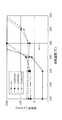
- FIG. 8is a diagram illustrating a relationship between the heating temperature and the resistivity of the source electrode and the drain electrode of the thin film transistor according to the embodiment.
- FIG. 9is a diagram illustrating a relationship between the film thickness of the first layer (upper layer) and the resistivity in the source electrode and the drain electrode of the thin film transistor according to the embodiment.
- FIG. 10is a cross-sectional view of a thin film transistor according to another embodiment.
- FIG. 1is a partially cutaway perspective view of an organic EL display device according to an embodiment.
- FIG. 2is a perspective view illustrating an example of a pixel bank of the organic EL display device according to the embodiment.
- an organic EL display device 1includes a thin film transistor array device (TFT array substrate) 2 in which a plurality of thin film transistors are arranged, an anode 51 as a lower electrode, and a light emitting layer made of an organic material, from the lower layer. It is constituted by a laminated structure of an organic EL element (light emitting part) 5 comprising a certain EL layer 52 and a cathode 53 which is a transparent upper electrode.
- the thin film transistor array device 2has a plurality of pixels 3 arranged in a matrix, and each pixel 3 is provided with a pixel circuit 4.
- the organic EL element 5is formed corresponding to each of the plurality of pixels 3, and the light emission of each organic EL element 5 is controlled by the pixel circuit 4 provided in each pixel 3.
- the organic EL element 5is formed on an interlayer insulating film (planarization film) formed so as to cover a plurality of thin film transistors.
- the organic EL element 5has a configuration in which an EL layer 52 is disposed between a pair of electrodes, that is, an anode 51 and a cathode 53.
- a positive electrodeis further provided between the anode 51 and the EL layer 52.
- a hole transport layeris laminated, and an electron transport layer is further laminated between the EL layer 52 and the cathode 53.
- another organic functional layermay be provided between the anode 51 and the cathode 53.
- Each pixel 3is driven and controlled by the respective pixel circuit 4. Further, in the thin film transistor array device 2, a plurality of gate wirings (scanning lines) 6 arranged along the row direction of the pixels 3 and a column direction of the pixels 3 so as to intersect the gate wiring 6 are arranged. A plurality of source lines (signal lines) 7 and a plurality of power supply lines (not shown in FIG. 1) arranged in parallel with the source lines 7 are formed. Each pixel 3 is partitioned by, for example, an orthogonal gate line 6 and a source line 7.
- the gate wiring 6is connected to each gate electrode of a thin film transistor that operates as a switching element included in each pixel circuit 4.
- the source wiring 7is connected to the source electrode of the thin film transistor operating as a switching element included in each pixel circuit 4 for each column.
- the power supply wiringis connected to the drain electrode of the thin film transistor operating as a driving element included in each pixel circuit 4 for each column.
- each pixel 3 of the organic EL display device 1is composed of sub-pixels 3R, 3G, and 3B of three colors (red, green, and blue), and these sub-pixels 3R, 3G, and 3B. Are formed in a matrix on the display surface.
- the sub-pixels 3R, 3G, and 3Bare separated from each other by the bank 3a.
- the banks 3aare formed in a lattice shape so that the ridges extending in parallel to the gate wiring 6 and the ridges extending in parallel to the source wiring 7 intersect each other.
- each of the portions surrounded by the protrusionsthat is, the opening of the bank 3a
- each of the sub-pixels 3R, 3G, and 3Bhave a one-to-one correspondence.
- the bank 3ais a pixel bank, but may be a line bank.
- the anode 51is formed for each of the sub-pixels 3R, 3G, and 3B on the interlayer insulating film (planarizing film) on the thin film transistor array device 2 and in the opening of the bank 3a.
- the EL layer 52is formed for each of the sub-pixels 3R, 3G, and 3B on the anode 51 and in the opening of the bank 3a.
- the transparent cathode 53is continuously formed on the plurality of banks 3a so as to cover all the EL layers 52 (all the sub-pixels 3R, 3G, and 3B).
- the pixel circuit 4is provided for each of the sub-pixels 3R, 3G, and 3B, and each of the sub-pixels 3R, 3G, and 3B and the corresponding pixel circuit 4 are electrically connected by a contact hole and a relay electrode.
- the sub-pixels 3R, 3G, and 3Bhave the same configuration except that the emission color of the EL layer 52 is different.
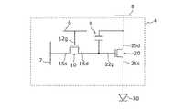
- FIG. 3is an electric circuit diagram showing a configuration of a pixel circuit in the organic EL display device according to the embodiment.
- the pixel circuit 4includes a thin film transistor 10 that operates as a switching element, a thin film transistor 20 that operates as a drive element, and a capacitor 9 that stores data to be displayed on the corresponding pixel 3.
- the thin film transistor 10is a switching transistor for selecting the pixel 3
- the thin film transistor 20is a drive transistor that drives the organic EL element 5.
- the thin film transistor 10includes a gate electrode 12g connected to the gate wiring 6, a source electrode 15s connected to the source wiring 7, a drain electrode 15d connected to the gate electrode 22g of the capacitor 9 and the thin film transistor 20, and a semiconductor film (FIG. Not shown).
- a voltageis applied to the connected gate line 6 and source line 7, the thin film transistor 10 stores the voltage value applied to the source line 7 in the capacitor 9 as display data.
- the thin film transistor 20includes a gate electrode 22g connected to the drain electrode 15d of the thin film transistor 10, a drain electrode 25d connected to the power supply wiring 8 and the capacitor 9, a source electrode 25s connected to the anode 51, and a semiconductor film (not shown). Z).
- the thin film transistor 20supplies a current corresponding to the voltage value held by the capacitor 9 from the power supply wiring 8 to the anode 51 through the source electrode 25s. As a result, a drive current flows from the anode 51 to the cathode 53, and the EL layer 52 emits light.
- the organic EL display device 1having the above configuration employs an active matrix system in which display control is performed for each pixel 3 located at the intersection of the gate wiring 6 and the source wiring 7. Thereby, the corresponding organic EL element 5 selectively emits light by the thin film transistors 10 and 20 of each pixel 3 (each sub-pixel 3R, 3G, and 3B), so that a desired image can be displayed.
- FIG. 4is a schematic cross-sectional view of the thin film transistor according to the embodiment.
- the thin film transistor 20 in the organic EL display device 1will be described, but the thin film transistor 10 can have the same configuration. That is, the thin film transistor described below can be applied to both a switching transistor and a driving transistor.
- the oxide semiconductor layer with high carrier mobilityis used as the channel layer, it is preferable to use the oxide semiconductor layer for a driving transistor.
- the thin film transistor 20includes a substrate 21, a gate electrode 22g formed above the substrate 21, an oxide semiconductor layer 24 that is a channel layer formed above the substrate 21, and a gate electrode 22g.
- a protective film 26 for coveringis a protective film 26 for covering.
- the thin film transistor 20 according to the present embodimentis a channel etching type bottom gate type thin film transistor, and a gate insulating film 23 is formed so as to cover the gate electrode 22g formed on the substrate 21.
- An oxide semiconductor layer 24is formed in an island shape over the film 23.
- the pair of the source electrode 25s and the drain electrode 25dare disposed on the oxide semiconductor layer 24 so as to face each other with a predetermined interval in the substrate horizontal direction.
- the surface of the gate insulating film 23extends from the surface of the end portion of the oxide semiconductor layer 24 so as to cover both ends of the oxide semiconductor layer 24. Is formed over. That is, the source electrode 25 s and the drain electrode 25 d are not only in contact with the oxide semiconductor layer 24 but are also in contact with the gate insulating film 23.
- the source electrode 25s and the drain electrode 25dare directly connected to the oxide semiconductor layer 24 so as to be in contact with the oxide semiconductor layer 24; however, the oxide semiconductor layer 24, the source electrode 25s, and Another layer may be provided between the drain electrode 25d and the source electrode 25s, the drain electrode 25d, and the oxide semiconductor layer 24 may be indirectly connected. At least the oxide semiconductor layer 24 and the source electrode 25s (drain electrode 25d) may be electrically connected so that carriers can move.
- the protective film 26is formed on the source electrode 25s, the drain electrode 25d, and the oxide semiconductor layer 24 so as to cover them. Since the thin film transistor 20 in this embodiment is a channel etching type, the protective film 26 is in contact with not only the source electrode 25s and the drain electrode 25d but also the oxide semiconductor layer 24 between the source electrode 25s and the drain electrode 25d. .
- the protective film 26is formed for the purpose of insulation from the electrode of the organic EL element (light emitting layer) formed on the upper layer of the thin film transistor 20. Although not shown, a contact hole is formed in the protective film 26, and the source electrode 25s or the drain electrode 25d is electrically connected to the electrode (for example, an anode) of the upper organic EL element through the contact hole.
- a glass substrateis used as the substrate 21.
- a resin substratemay be used.
- An undercoat layermay be formed on the surface of the substrate 21.
- the gate electrode 22gfor example, a metal such as Ti, Mo, W, Al, or Au, or a conductive oxide such as ITO (indium tin oxide) is used.
- a metalsuch as Ti, Mo, W, Al, or Au
- a conductive oxidesuch as ITO (indium tin oxide)
- an alloysuch as MoW
- a metal laminate in which, for example, Ti, Al, Au or the like is sandwiched as a metal having good adhesion to the oxidecan be used as the gate electrode 22g.
- an oxide thin filmsuch as a silicon oxide film or a hafnium oxide film, a nitride film such as a silicon nitride film or a single layer film of a silicon oxynitride film, or a laminated film thereof is used.
- the oxide semiconductor layer 24is preferably formed using a transparent amorphous oxide semiconductor such as InGaZnO x (IGZO) containing In—Ga—Zn—O.
- IGZOInGaZnO x
- a thin film transistor using a transparent amorphous oxide semiconductor as a channel layerhas high carrier mobility and is suitable for a large-screen and high-definition display device. Further, since the transparent amorphous oxide semiconductor can be formed at a low temperature, it can be easily formed on a flexible substrate such as a plastic or a film.
- An amorphous oxide semiconductor film of InGaZnO X containing In—Ga—Zn—Ois formed by vapor phase deposition such as sputtering or laser deposition using, for example, a polycrystalline sintered body having an InGaO 3 (ZnO) 4 composition.
- the filmcan be formed by a film method.
- the film thickness of the oxide semiconductor layer 24is preferably 10 nm to 150 nm. When the film thickness is less than 10 nm, pinholes are likely to occur, and when the film thickness is more than 150 nm, the leakage current and subthreshold swing value (S value) during off operation increase, and transistor characteristics Deteriorates.
- the atomic concentration of Cu in the channel region between the source electrode 25s and the drain electrode 25dis preferably 1 ⁇ 10 ⁇ 19 / cm 3 or less. If the atomic concentration (contamination amount) of Cu is large, the leakage current increases, resulting in a change in transistor characteristics and an increase in power consumption of the thin film transistor 20.
- the atomic concentration (contamination amount) of Cuis determined by using secondary ion mass spectrometry (SIMS), that is, by irradiating ions (primary ions) to the sample surface, ions (secondary ions) among the particles that have jumped out.
- SIMSsecondary ion mass spectrometry
- mass spectrometryit can be measured and evaluated using a method for qualitative and quantitative determination of components contained in a sample.
- Each of the source electrode 25s and the drain electrode 25dis made of a material containing Cu. Specifically, each of the source electrode 25s and the drain electrode 25d is a stacked film including three layers of a first layer 251, a second layer 252, and a third layer 253. Note that the source electrode 25s and the drain electrode 25d are not limited to a three-layer structure, and may include other layers.
- the first layer 251which is a lower layer is an adhesion layer with the base layer, and is formed on the oxide semiconductor layer 24 and the gate insulating film 23.
- the first layer 251also functions as a Cu diffusion suppression layer that suppresses diffusion of Cu atoms of the second layer 252 into the oxide semiconductor layer 24.
- the second layer 252which is an intermediate layer is a main wiring layer containing Cu as a main component, and is in contact with the first layer 251 and the third layer 253, and the first layer 251 and the third layer 253 Formed between.
- Cuas the main wiring material, the resistance can be reduced.
- the upper third layer 253is a cap layer that protects the main wiring layer, and is formed on the second layer 252.
- a laminated film(CuMn alloy film / Cu film) in which a Mo (molybdenum) film, a Cu (copper) film, and a CuMn (copper manganese) alloy film are laminated in this order from the bottom to the top. / Mo film).
- the first layer 251is a Mo film
- the second layer 252is a Cu film
- the third layer 253is a CuMn alloy film, and these layers are stacked above the substrate 21.
- the CuMn alloy filmmeans an alloy film of copper and manganese. The same applies to the following.
- the source electrode 25s and the drain electrode 25dinclude a laminated film (CuMn alloy film / Cu film / CuMn alloy film) in which a CuMn alloy film, a Cu film, and a CuMn alloy film are laminated in this order from the bottom to the top. It can be.
- the first layer 251is a CuMn alloy film
- the second layer 252is a Cu film
- the third layer 253is a CuMn alloy film
- these layersare stacked toward the upper side of the substrate 21. Can be formed.
- the first layer (lower layer) 251by forming a Mo film or a CuMn alloy film as the first layer (lower layer) 251, it is possible to suppress the diffusion of Cu atoms in the second layer 252 to the oxide semiconductor layer 24. Furthermore, by forming a Mo film or a CuMn alloy film as the first layer (lower layer) 251, adhesion with the base layer (the oxide semiconductor layer 24 and the gate insulating film 23) can be improved.
- the third layer (upper layer) 252by forming a CuMn alloy film as the third layer (upper layer) 252, it is possible to suppress the Cu atoms of the second layer 252 from being oxidized and the second layer 252 from being altered. Thereby, the high resistance of the source electrode 25s and the drain electrode 25d due to Cu oxidation can be suppressed.
- the protective film 26for example, a resin-coated photosensitive insulating material containing silsesioxene, acrylic, or siloxane that can attenuate light having a wavelength of 450 nm or less is used. Further, the protective film 26 may be a laminated film of the photosensitive insulating material and the inorganic insulating material. For example, silicon oxide, aluminum oxide, titanium oxide, or the like is used as the inorganic insulating material. In addition, a CVD method, a sputtering method, an ALD method, or the like is used for forming the inorganic insulating material.
- FIGS. 5A to 5Kare cross-sectional views of each step in the method of manufacturing the thin film transistor according to the embodiment.
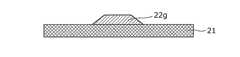
- a substrate 21is prepared, and a gate electrode 22g is processed into a desired shape above the substrate 21.
- a gate metal filmis formed on the substrate 21 by sputtering, and the gate metal film 22 is patterned by using a photolithography method and a wet etching method, thereby forming a gate electrode 22g having a predetermined shape.
- a gate insulating filmis formed above the substrate 21.
- the gate insulating film 23 made of silicon oxideis formed by plasma CVD or the like so as to cover the gate electrode 22g.
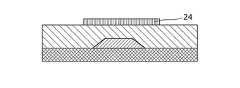
- an oxide semiconductor layer 24 having a predetermined shapeis formed above the substrate 21.
- the oxide semiconductor layer 24is formed over the gate insulating film 23.
- the oxide semiconductor layer 24 made of a transparent amorphous oxide semiconductor of InGaZnO Xis formed by the above-described film formation method.
- a resist pattern R1is formed on the oxide semiconductor layer 24 in order to process the oxide semiconductor layer 24 into a predetermined shape.
- the oxide semiconductor layer 24is patterned using the resist pattern R1 to process the oxide semiconductor layer 24 into a predetermined shape.
- a wet etching methodis used for processing the oxide semiconductor layer 24.
- an acid mixed solution containing phosphoric acid, nitric acid, acetic acid, or the like, or oxalic acid, hydrochloric acid, or the likeis used.
- the resist pattern R1is removed.
- wet etching using a resist stripping solution, dry etching using O 2 plasma, or the likeis used.
- the oxide semiconductor layer 24 having a predetermined shapecan be formed.
- the oxide semiconductor layer 24is formed in an island shape.
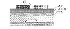
- the laminated film 25is formed and processed to form a pair of source electrode 25s and drain electrode 25d.
- a first layer 251, a second layer 252, and a third layer 253are sequentially formed as a laminated film (electrode film) 25 to be the source electrode 25s and the drain electrode 25d.
- Filmfor example, a Mo film or a CuMn alloy film is formed as the first layer 251, a Cu film is formed as the second layer 252, and a CuMn alloy film is formed as the third layer 253.
- These filmscan be sequentially formed by sputtering, for example.
- the first layer 251plays the role of suppressing the diffusion of Cu into the oxide semiconductor layer 24 and the role of improving the adhesion with the oxide semiconductor layer 24.
- the third layer (upper layer) 253plays a role of suppressing deterioration due to oxidation of the second layer (Cu film) 252 serving as the main wiring layer.
- a resist pattern R2is formed on the laminated film 25 in order to process the laminated film 25 into a source electrode 25s and a drain electrode 25d having a predetermined shape.
- the laminated film 25is patterned using the resist pattern R2 to process the laminated film 25 into a source electrode 25s and a drain electrode 25d having a predetermined shape.
- a wet etching methodis used for processing the laminated film 25.
- the resist pattern R2is removed.
- the removal of the resist pattern R2can use the same method as the removal of the resist pattern R1.
- a pair of source electrode 25s and drain electrode 25d having a predetermined shapecan be formed.
- the oxide semiconductor layer 24is preferably heat-treated at 150 to 450 ° C. for 0.5 to 1200 minutes. By performing this heat treatment, the contact resistance value between the oxide semiconductor layer 24 and the source electrode 25s or the drain electrode 25d can be reduced, and the characteristics of the oxide semiconductor layer 24 can be stabilized.
- a protective film 26is formed so as to cover the source electrode 25s and the drain electrode 25d. Thereby, the thin film transistor 20 is completed.
- an electrical contact between the upper layer electrode and the source electrode 25s or the drain electrode 25d or an electrical contact between the upper layer electrode and the gate electrode 22gis formed.
- a contact holeis formed in The contact hole can be formed by photolithography using a photosensitive material as the protective film 26.
- the wiringtends to become long and thin due to the large screen and high definition of the display device. For this reason, there exists a subject that wiring resistance becomes high and the quality of a display image deteriorates.
- a part of the source electrode and the drain electrode in the thin film transistormay be extended to function as a wiring. Therefore, the material and the structure of the source electrode and the drain electrode are not only the performance as a thin film transistor but also the wiring. Performance is also required.
- the adhesion between the source electrode and the drain electrode with the base layeris important.
- the source electrode and the drain electrodeare peeled off, and the transistor characteristics are greatly deteriorated.
- the channel layeris an oxide semiconductor
- the transistor characteristicsare deteriorated due to an increase in contact resistance.
- the inventors of the present applicationpay attention to the problems of the various aspects described above, and when the oxide semiconductor layer is used as the channel layer and the low resistance Cu is used as the main wiring material of the source electrode and the drain electrode, the source electrode In addition, an electrode structure and a metal material suitable as a drain electrode were studied.
- the inventors of the present applicationuse a laminated film of a Mo film, a Cu film, and a CuMn alloy film or a laminated film of a CuMn alloy film, a Cu film, and a CuMn alloy film as a source electrode and a drain electrode.
- the inventorshave found that desired transistor characteristics can be obtained.
- FIG. 6shows the result of the study, and is a comparative table of the film structures of the source electrode and the drain electrode.
- FIG. 6shows five examples of the source electrode and drain electrode whose main wiring layer is a Cu film.
- the lower layeris the first layer 251
- the main wiring layeris the second layer 252
- the upper layeris the third layer 253.
- adhesionrefers to evaluation of whether the source or drain electrode and the base layer (oxide semiconductor layer, gate insulating film) are in close contact with each other. Moreover, heat resistance evaluated whether the source electrode and the drain electrode can withstand the temperature (for example, the upper limit of 300 ° C.) of the heat treatment process or the oxidation process in the TFT manufacturing process (particularly heat resistance in an oxidizing atmosphere).
- the processing shape propertyis an evaluation of whether the shape of the source electrode and the drain electrode after processing is normal, or whether a predetermined processing can be performed when patterning the source electrode and the drain electrode. . Moreover, evaluation of (circle) means that there was no problem in all, and evaluation of * means that there was some problem.
- Comparative Example 1has a two-layer structure of a Cu film (main wiring layer) and a CuMn alloy film (upper layer), and a cap layer made of a CuMn alloy film is formed on the Cu film in order to suppress oxidation of the Cu film. It has become the composition. In this case, there was no problem in heat resistance and processing shape, but Cu was difficult to adhere to the oxide semiconductor layer, and there was a problem in adhesion.
- Comparative Example 2has a two-layer structure of a Mo film (lower layer) and a Cu film (main wiring layer), in which a Mo film is formed under the Cu film in order to improve adhesion with the oxide semiconductor layer. It has become. In this case, there was no problem with the adhesion and processing shape, but there was a problem with heat resistance.
- Comparative Example 3has a three-layer structure of a Mo film (lower layer), a Cu film (main wiring layer), and a Mo film (upper layer).
- a Mo filmis used as a lower layer in order to improve adhesion. It is the structure which formed.
- Example 1has a three-layer structure of a Mo film (lower layer), a Cu film (main wiring layer), and a CuMn alloy film (upper layer).
- the upper layeris changed from a Mo film to a CuMn alloy film. It has become.
- the upper CuMn alloy filmcan suppress the oxidation of the Cu film, and there is no problem in any of adhesion, heat resistance, and processing shape. That is, in Example 1, the battery reaction as in Comparative Example 3 did not occur, and no abnormality occurred in the processed shape.
- Example 2has a three-layer structure of a CuMn alloy film (lower layer), a Cu film (main wiring layer), and a CuMn alloy film (upper layer).
- the upper and lower Mo filmswere changed to a CuMn alloy film. It has a different configuration. With this configuration, the upper CuMn alloy film can suppress the oxidation of the Cu film, and there is no problem in any of adhesion, heat resistance, and processing shape. In Example 2, no battery reaction occurred, and no abnormality occurred in the processed shape.
- Example 1 or Example 2are applied to the source electrode 25s and the drain electrode 25d of the thin film transistor 20 shown in FIG. It was found that the source electrode 25s and the drain electrode 25d excellent in heat resistance and processing shape can be realized.
- the source electrode 25s and the drain electrode 25d connected to the oxide semiconductor layer 24include a stacked film of a Mo film, a Cu film, and a CuMn alloy film, and a CuMn alloy film and a Cu film.
- a stacked film of a Mo film, a Cu film, and a CuMn alloy film, and a CuMn alloy film and a Cu filmOne of the laminated films of the film and the CuMn alloy film is included.
- the desired processing shape of the source electrode 25s and the drain electrode 25dcan be obtained.
- the source electrode 25sthat is a thin film transistor using an oxide semiconductor as a channel layer, is a low-resistance wiring, and has excellent adhesion, heat resistance, and processed shape. Desired transistor characteristics can be obtained while realizing the drain electrode 25d.
- FIG. 7is an enlarged view of a region A surrounded by a broken line in FIG. 5K, and is an enlarged cross-sectional view around the source electrode 25s.
- An interface layer 254is also formed in the drain electrode 25d.
- an interface layer 254 made of MnSiO having a thickness of about 5 nm to 10 nmis formed at the interface between the protective film 26 made of a silicon oxide film and the third layer (upper layer) 253 made of a CuMn alloy film. It was found that it was formed. That is, it was found that the source electrode 25s is a laminated film in which the Mo film, the Cu film, the CuMn alloy film, and the MnSiO film are laminated in this order from the bottom to the top.
- This interface layer 254is considered to be a layer formed by combining the Mn component of the third layer 253, which is a CuMn alloy film, and the Si component and O component of the protective film 26, which is a silicon oxide film. It is considered that the performance of the source electrode 25s and the drain electrode 25d is further improved by forming the interface layer (MnSiO film) 254.
- the Mn concentrationis 0% (Cu)
- the Mn concentrationis 4% (CuMn4%)
- the Mn concentrationis 8% (CuMn8%)
- the Cu concentrationis 10% (CuMn10%).
- Each of the four CuMn single layer filmswas measured for resistivity values when the heating temperature was 100 ° C, 200 ° C, 250 ° C, 300 ° C, 350 ° C.
- heat resistance of 300 ° C.is required due to the upper limit of the process temperature after wiring formation.
- the film forming temperature of the protective film 26is 300 ° C. at the maximum. From this, it is preferable that the CuMn alloy film has a stable resistivity at 300 ° C. or lower.
- the Mn concentration of the CuMn alloy filmis at least 8% and 10%, no change in resistivity is observed when the heating temperature is 300 ° C. or lower. That is, by setting the Mn concentration of the CuMn alloy film to at least 8% or more, heat resistance that can withstand the upper limit temperature of the TFT process can be ensured.
- the Mn concentration of the CuMn alloy filmis preferably 8% or more. From the viewpoint of the upper limit for producing a large target, the Mn concentration of the CuMn alloy film is preferably 15% or less for practical use.
- the results of an experiment conducted on the thickness of the third layer (upper layer) 253will be described with reference to FIG.
- the source electrode 25s (drain electrode 25d)has a structure of a Mo film (lower layer), a Cu film, and a CuMn alloy film (upper layer)
- the third layer 253 (CuMn alloy film) as a cap layeris formed.
- the change in sheet resistance of the source electrode 25s (drain electrode 25d) due to the presence or absence of heat treatment when the film thickness was changedwas examined.
- the resistivity valueswere measured when the thickness of the CuMn alloy film was 30 nm, 40 nm, 50 nm, 60 nm, 80 nm, and 100 nm.
- the third layer 253As shown in FIG. 9, when the thickness of the third layer 253 (CuMn alloy film) as a cap layer is thin, the resistivity increases when heated at the upper limit temperature (300 ° C.) of the process after the wiring formation. I understand that.
- the wiring resistance in the display deviceis required to be 0.07 ⁇ / ⁇ or less, as shown in FIG. 9, the third layer 253 is used to ensure heat resistance.
- the film thickness of the CuMn alloy filmis preferably 50 nm or more.
- the thickness of the third layer 253(CuMn alloy film) is preferably 100 nm or less.
- the film thickness of the lower first layer 251is preferably 20 nm to 60 nm in the case of a CuMn alloy film, and 10 nm to 40 nm in the case of a Mo film. By setting the film thickness within this range, desired transistor characteristics can be obtained.
- the thickness of the second layer 252 that is a Cu filmis preferably set to 300 nm or more.
- the thin film transistorAs described above, the thin film transistor, the method for manufacturing the thin film transistor, and the organic EL display device have been described based on the embodiments. However, the present invention is not limited to the above embodiments.
- the thin film transistor 20is a bottom gate type TFT, it may be a top gate type TFT as shown in FIG.
- a thin film transistor 20A according to the modification shown in FIG. 10includes a substrate 21, an undercoat layer 27 formed on the substrate 21, an oxide semiconductor layer 24 formed on the undercoat layer 27, and an oxide semiconductor layer. 24, the gate insulating film 23 formed so as to cover the gate electrode 24, the gate electrode 22g formed on the gate insulating film 23 above the oxide semiconductor layer 24, and the gate insulating film 23 so as to cover the gate electrode 22g. Formed on the interlayer insulating film 28, the source electrode 25s and the drain electrode 25d connected to the oxide semiconductor layer 24, and the source electrode 25s and the drain electrode 25d.
- the protective film 26is provided.
- the source electrode 25s and the drain electrode 25dare formed of the first layer 251 (Mo film or CuMn alloy film), the second layer 252 (Cu film), and the third layer 253 (CuMn alloy film). ) And a laminated film laminated in this order from the bottom to the top.
- the third layer 253is embedded in a contact hole formed in the interlayer insulating film 28 and the gate insulating film 23 and connected to the oxide semiconductor layer 24.
- the thin film transistor 20is a channel etching type TFT, but may be a channel etching stopper type (channel protection type) TFT.
- a SiO 2 thin film or the likeis formed on the oxide semiconductor layer 24 as a channel etching stopper (channel protective film).
- the source electrode 25s and the drain electrode 25dare the same laminated film, but they may be different laminated films.
- the source electrode 25smay be a laminated film of a Mo film, a Cu film, and a CuMn alloy film
- the drain electrode 25dmay be a laminated film of a CuMn alloy film, a Cu film, and a CuMn alloy film.
- the source electrode 25smay be a stacked film of a CuMn alloy film, a Cu film, and a CuMn alloy film
- the drain electrode 25dmay be a stacked film of a Mo film, a Cu film, and a CuMn alloy film.
- an organic EL display device using an organic EL elementis described as a display device using a thin film transistor.
- the thin film transistor 20 in the above embodimentis an active matrix substrate (thin film transistor) such as a liquid crystal display element.
- the present inventioncan also be applied to a display device including other display elements in which an array device is used.
- the display devicesuch as the organic EL display device described above can be used as a flat panel display and applied to all electronic devices having a display panel, such as a television set, a personal computer, and a mobile phone. can do. In particular, it is suitable for a large-screen and high-definition display device.
- the technique disclosed hereincan be widely used in a thin film transistor using an oxide semiconductor, a manufacturing method thereof, a display device such as an organic EL display device using the thin film transistor, and the like.
Landscapes
- Electrodes Of Semiconductors (AREA)
- Thin Film Transistor (AREA)
- Electroluminescent Light Sources (AREA)
Abstract
Description
Translated fromJapaneseここに開示された技術は、液晶表示装置や有機EL(Electro-Luminescence)表示装置等に用いられる薄膜トランジスタ及びこれを用いた有機EL表示装置、並びに薄膜トランジスタの製造方法に関する。The technology disclosed herein relates to a thin film transistor used in a liquid crystal display device, an organic EL (Electro-Luminescence) display device, and the like, an organic EL display device using the thin film transistor, and a method of manufacturing the thin film transistor.
液晶表示装置や有機EL表示装置等のアクティブマトリクス方式の表示装置には、スイッチング素子又は駆動素子として薄膜トランジスタ(TFT:Thin Film Transistor)と呼ばれる薄膜半導体装置が用いられる。2. Description of the Related Art In an active matrix display device such as a liquid crystal display device or an organic EL display device, a thin film semiconductor device called a thin film transistor (TFT) is used as a switching element or a driving element.
薄膜トランジスタの構成には、ゲート電極がチャネル層の下方(基板側)に形成された構造であるボトムゲート型の薄膜トランジスタ、あるいは、ゲート電極がチャネル層の上方に形成された構造であるトップゲート型の薄膜トランジスタがある。薄膜トランジスタのチャネル層には、例えばシリコン半導体又は酸化物半導体が用いられる。The configuration of the thin film transistor includes a bottom gate type thin film transistor having a structure in which a gate electrode is formed below the channel layer (substrate side), or a top gate type having a structure in which the gate electrode is formed above the channel layer. There is a thin film transistor. For example, a silicon semiconductor or an oxide semiconductor is used for the channel layer of the thin film transistor.
また、ボトムゲート型の薄膜トランジスタは、チャネル層がエッチングされるチャネルエッチング構造のものと、ソース電極及びドレイン電極を形成する際のチャネル層へのダメージを抑制するためにチャネルエッチングストッパーを形成するチャネルエッチングストッパー構造のものとの2つに大別される。The bottom gate type thin film transistor includes a channel etching structure in which the channel layer is etched and a channel etching in which a channel etching stopper is formed to suppress damage to the channel layer when forming the source electrode and the drain electrode. There are roughly two types, one with a stopper structure.
例えば、特許文献1には、チャネル層が酸化物半導体であるチャネルエッチングストッパー構造の薄膜トランジスタが開示されている。チャネルエッチングストッパーとしては、例えば、チャネルエッチングストッパー形成時に酸化物半導体が還元性ガスにより特性変動を起こすことを防止するために、SiO2薄膜が用いられる。For example,
ここに開示された技術は、所望のトランジスタ特性を得ることを目的とするものである。The technique disclosed herein is intended to obtain desired transistor characteristics.
上記課題を解決する薄膜トランジスタの一態様は、基板の上方に形成されたゲート電極と、前記基板の上方に形成された酸化物半導体層と、ゲート電極と前記酸化物半導体層との間に形成されたゲート絶縁膜と、酸化物半導体層に接続された複数の電極と、複数の電極を覆う保護膜とを有し、複数の電極のそれぞれは、Mo膜とCu膜とCuMn合金膜とが下から上にこの順序で積層された積層膜、又は、CuMn合金膜とCu膜とCuMn合金膜とが下から上にこの順序で積層された積層膜を含む。One embodiment of a thin film transistor that solves the above problem is formed between a gate electrode formed above a substrate, an oxide semiconductor layer formed above the substrate, and the gate electrode and the oxide semiconductor layer. A gate insulating film, a plurality of electrodes connected to the oxide semiconductor layer, and a protective film covering the plurality of electrodes. Each of the plurality of electrodes includes a Mo film, a Cu film, and a CuMn alloy film. Or a laminated film in which a CuMn alloy film, a Cu film, and a CuMn alloy film are laminated in this order from the bottom to the top.
所望のトランジスタ特性を有する薄膜トランジスタを提供することが可能となる。It is possible to provide a thin film transistor having desired transistor characteristics.
以下、薄膜トランジスタ、薄膜トランジスタの製造方法及び薄膜トランジスタを用いた有機EL表示装置の一実施の形態について、図面を用いて説明する。なお、以下に説明する実施の形態は、いずれも本発明の好ましい一具体例を示すものである。したがって、以下の実施の形態で示される、数値、形状、材料、構成要素、構成要素の配置位置及び接続形態、工程(ステップ)、工程の順序などは、一例であって本発明を限定する主旨ではない。よって、以下の実施の形態における構成要素のうち、本発明の最上位概念を示す独立請求項に記載されていない構成要素については、任意の構成要素として説明される。Hereinafter, embodiments of a thin film transistor, a method for manufacturing the thin film transistor, and an organic EL display device using the thin film transistor will be described with reference to the drawings. Note that each of the embodiments described below shows a preferred specific example of the present invention. Accordingly, the numerical values, shapes, materials, components, arrangement positions and connection forms of components, steps (steps), order of steps, and the like shown in the following embodiments are merely examples and are intended to limit the present invention. is not. Therefore, among the constituent elements in the following embodiments, constituent elements that are not described in the independent claims showing the highest concept of the present invention are described as optional constituent elements.
なお、各図は、模式図であり、必ずしも厳密に図示されたものではない。また、各図において、実質的に同一の構成に対しては同一の符号を付しており、重複する説明は省略又は簡略化する。Each figure is a schematic diagram and is not necessarily shown strictly. Moreover, in each figure, the same code | symbol is attached | subjected to the substantially same structure, The overlapping description is abbreviate | omitted or simplified.
(有機EL表示装置)
まず、実施の形態に係る有機EL表示装置1の構成について、図1及び図2を用いて説明する。図1は、実施の形態に係る有機EL表示装置の一部切り欠き斜視図である。図2は、実施の形態に係る有機EL表示装置のピクセルバンクの例を示す斜視図である。(Organic EL display device)
First, the configuration of the organic
図1に示すように、有機EL表示装置1は、下層より、複数個の薄膜トランジスタが配置された薄膜トランジスタアレイ装置(TFTアレイ基板)2と、下部電極である陽極51、有機材料からなる発光層であるEL層52及び透明な上部電極である陰極53からなる有機EL素子(発光部)5との積層構造により構成される。As shown in FIG. 1, an organic
薄膜トランジスタアレイ装置2には複数の画素3がマトリクス状に配置されており、各画素3には画素回路4が設けられている。The thin film
有機EL素子5は、複数の画素3のそれぞれに対応して形成されており、各画素3に設けられた画素回路4によって各有機EL素子5の発光の制御が行われる。有機EL素子5は、複数の薄膜トランジスタを覆うように形成された層間絶縁膜(平坦化膜)の上に形成される。The
また、有機EL素子5は、一対の電極である陽極51と陰極53との間にEL層52が配置された構成となっており、例えば、陽極51とEL層52との間にはさらに正孔輸送層が積層形成され、EL層52と陰極53との間にはさらに電子輸送層が積層形成されている。なお、陽極51と陰極53との間には、その他の有機機能層が設けられていてもよい。The
各画素3は、それぞれの画素回路4によって駆動制御される。また、薄膜トランジスタアレイ装置2には、画素3の行方向に沿って配置される複数のゲート配線(走査線)6と、ゲート配線6と交差するように画素3の列方向に沿って配置される複数のソース配線(信号配線)7と、ソース配線7と平行に配置される複数の電源配線(図1では省略)とが形成されている。各画素3は、例えば直交するゲート配線6とソース配線7とによって区画されている。Each
ゲート配線6は、各画素回路4に含まれるスイッチング素子として動作する薄膜トランジスタのゲート電極と行毎に接続されている。ソース配線7は、各画素回路4に含まれるスイッチング素子として動作する薄膜トランジスタのソース電極と列毎に接続されている。電源配線は、各画素回路4に含まれる駆動素子として動作する薄膜トランジスタのドレイン電極と列毎に接続されている。The
図2に示すように、有機EL表示装置1の各画素3は、3色(赤色、緑色、青色)のサブ画素3R、3G、3Bによって構成されており、これらのサブ画素3R、3G、3Bは、表示面上に複数個マトリクス状に配列されるように形成されている。各サブ画素3R、3G、3Bは、バンク3aによって互いに分離されている。バンク3aは、ゲート配線6に平行に延びる突条と、ソース配線7に平行に延びる突条とが互いに交差するように、格子状に形成されている。そして、この突条で囲まれる部分(すなわち、バンク3aの開口部)の各々とサブ画素3R、3G、3Bの各々とが一対一で対応している。なお、本実施の形態において、バンク3aはピクセルバンクとしたが、ラインバンクとしても構わない。As shown in FIG. 2, each
陽極51は、薄膜トランジスタアレイ装置2上の層間絶縁膜(平坦化膜)上でかつバンク3aの開口部内に、サブ画素3R、3G、3B毎に形成されている。同様に、EL層52は、陽極51上でかつバンク3aの開口部内に、サブ画素3R、3G、3B毎に形成されている。透明な陰極53は、複数のバンク3a上で、かつ全てのEL層52(全てのサブ画素3R、3G、3B)を覆うように、連続的に形成されている。The
さらに、画素回路4は、各サブ画素3R、3G、3B毎に設けられており、各サブ画素3R、3G、3Bと、対応する画素回路4とは、コンタクトホール及び中継電極によって電気的に接続されている。なお、サブ画素3R、3G、3Bは、EL層52の発光色が異なることを除いて同一の構成である。Furthermore, the
ここで、画素3における画素回路4の回路構成について、図3を用いて説明する。図3は、実施の形態に係る有機EL表示装置における画素回路の構成を示す電気回路図である。Here, the circuit configuration of the
図3に示すように、画素回路4は、スイッチング素子として動作する薄膜トランジスタ10と、駆動素子として動作する薄膜トランジスタ20と、対応する画素3に表示するためのデータを記憶するキャパシタ9とで構成される。本実施の形態において、薄膜トランジスタ10は、画素3を選択するためのスイッチングトランジスタであり、薄膜トランジスタ20は、有機EL素子5を駆動する駆動トランジスタである。As shown in FIG. 3, the
薄膜トランジスタ10は、ゲート配線6に接続されるゲート電極12gと、ソース配線7に接続されるソース電極15sと、キャパシタ9及び薄膜トランジスタ20のゲート電極22gに接続されるドレイン電極15dと、半導体膜(図示せず)とで構成される。この薄膜トランジスタ10は、接続されたゲート配線6及びソース配線7に電圧が印加されると、当該ソース配線7に印加された電圧値を表示データとしてキャパシタ9に保存する。The
薄膜トランジスタ20は、薄膜トランジスタ10のドレイン電極15dに接続されるゲート電極22gと、電源配線8及びキャパシタ9に接続されるドレイン電極25dと、陽極51に接続されるソース電極25sと、半導体膜(図示せず)とで構成される。この薄膜トランジスタ20は、キャパシタ9が保持している電圧値に対応する電流を電源配線8からソース電極25sを通じて陽極51に供給する。これにより、陽極51から陰極53へと駆動電流が流れてEL層52が発光する。The
なお、上記構成の有機EL表示装置1では、ゲート配線6とソース配線7との交点に位置する画素3毎に表示制御を行うアクティブマトリクス方式が採用されている。これにより、各画素3(各サブ画素3R、3G、3B)の薄膜トランジスタ10及び20によって、対応する有機EL素子5が選択的に発光することで、所望の画像を表示することができる。Note that the organic
(薄膜トランジスタ)
次に、実施の形態に係る薄膜トランジスタについて、図4を用いて説明する。図4は、実施の形態に係る薄膜トランジスタの概略断面図である。なお、以下の実施の形態では、上記有機EL表示装置1における薄膜トランジスタ20について説明するが、薄膜トランジスタ10も同様の構成とすることができる。つまり、以下に説明する薄膜トランジスタは、スイッチングトランジスタ及び駆動トランジスタのいずれにも適用することができる。ただし、キャリア移動度の高い酸化物半導体層をチャネル層としているので、駆動トランジスタに適用する方がよい。(Thin film transistor)
Next, a thin film transistor according to an embodiment will be described with reference to FIGS. FIG. 4 is a schematic cross-sectional view of the thin film transistor according to the embodiment. In the following embodiment, the
図4に示すように、薄膜トランジスタ20は、基板21と、基板21の上方に形成されたゲート電極22gと、基板21の上方に形成されたチャネル層である酸化物半導体層24と、ゲート電極22gと酸化物半導体層24との間に形成されたゲート絶縁膜23と、酸化物半導体層24に接続された複数の電極であるソース電極25s及びドレイン電極25dと、ソース電極25s及びドレイン電極25dを覆う保護膜26とを有する。As shown in FIG. 4, the
本実施の形態に係る薄膜トランジスタ20は、チャネルエッチング型でボトムゲート型の薄膜トランジスタであって、基板21上に形成されたゲート電極22gを覆うようにゲート絶縁膜23が形成されており、当該ゲート絶縁膜23上には酸化物半導体層24が島状に形成されている。The
一対のソース電極25s及びドレイン電極25dは、酸化物半導体層24上において基板水平方向に所定の間隔をあけて対向配置されている。本実施の形態における一対のソース電極25s及びドレイン電極25dの各々は、酸化物半導体層24の両端部の各々を覆うように、酸化物半導体層24の端部の表面からゲート絶縁膜23の表面にわたって形成されている。つまり、ソース電極25s及びドレイン電極25dは、酸化物半導体層24に接するだけではなく、ゲート絶縁膜23にも接している。The pair of the
なお、本実施の形態において、ソース電極25s及びドレイン電極25dは酸化物半導体層24と接するように酸化物半導体層24と直接的に接続されているが、酸化物半導体層24とソース電極25s及びドレイン電極25dとの間に別の層を設けて、ソース電極25s及びドレイン電極25dと酸化物半導体層24とが間接的に接続されていてもよい。少なくとも、キャリアが移動できるように酸化物半導体層24とソース電極25s(ドレイン電極25d)とが電気的に接続されていればよい。Note that in this embodiment, the
保護膜26は、ソース電極25s、ドレイン電極25d及び酸化物半導体層24上において、これらを覆うように形成されている。本実施の形態における薄膜トランジスタ20はチャネルエッチング型であるので、保護膜26は、ソース電極25s及びドレイン電極25dだけではなく、ソース電極25s及びドレイン電極25d間において酸化物半導体層24にも接している。The
保護膜26は、薄膜トランジスタ20の上部層に形成される有機EL素子(発光層)の電極との絶縁を図るなどを目的として形成されている。なお、図示していないが、保護膜26にはコンタクトホールが形成され、このコンタクトホールを通して、ソース電極25s又はドレイン電極25dと上部層の有機EL素子の電極(例えば陽極)と電気的に接続される。The
ここで、基板21としては、例えば、ガラス基板が用いられる。また、薄膜トランジスタ20をフレキシブルディスプレイに用いる場合には樹脂基板を用いてもよい。なお、基板21の表面にアンダーコート層を形成してもよい。Here, for example, a glass substrate is used as the
ゲート電極22gとしては、例えばTi、Mo、W、Al、Auなどの金属やITO(酸化インジウムスズ)などの導電酸化物が用いられる。また、金属に関しては、例えばMoWのような合金もゲート電極22gとして用いることができる。また、膜の密着性を高めるために、酸化物との密着性が良い金属として例えばTi、AlやAuなどを挟んだ金属の積層体をゲート電極22gとして用いることもできる。As the
ゲート絶縁膜23としては、例えば酸化シリコン膜や酸化ハフニウム膜などの酸化物薄膜、窒化シリコン膜などの窒化膜もしくはシリコン酸窒化膜の単層膜、又は、これらの積層膜などが用いられる。As the
酸化物半導体層24としては、In-Ga-Zn-Oを含むInGaZnOX(IGZO)などの透明アモルファス酸化物半導体により構成するのが望ましい。透明アモルファス酸化物半導体をチャネル層とする薄膜トランジスタは、キャリア移動度が高く、大画面及び高精細の表示装置に適している。また、透明アモルファス酸化物半導体は、低温成膜が可能であるため、プラスチックやフィルムなどのフレキシブル基板上に容易に形成することができる。The
In-Ga-Zn-Oを含むInGaZnOXのアモルファス酸化物半導体膜は、例えば、InGaO3(ZnO)4組成を有する多結晶焼結体をターゲットとして、スパッタ法やレーザー蒸着法などの気相成膜法により成膜することができる。An amorphous oxide semiconductor film of InGaZnOX containing In—Ga—Zn—O is formed by vapor phase deposition such as sputtering or laser deposition using, for example, a polycrystalline sintered body having an InGaO3 (ZnO)4 composition. The film can be formed by a film method.
酸化物半導体層24の膜厚は、10nm~150nmが好ましい。膜厚が10nmより薄い場合は、ピンホールが発生しやすくなり、また、膜厚が150nmより厚い場合は、オフ動作時のリーク電流やサブスレッシュホルドスウィング値(S値)が増大し、トランジスタ特性が劣化する。The film thickness of the
また、酸化物半導体層24は、ソース電極25s及びドレイン電極25d間のチャネル領域におけるCuの原子濃度が、1×10-19/cm3以下であることが好ましい。Cuの原子濃度(汚染量)が多いと、リーク電流が増大し、トランジスタ特性の変動をきたすとともに薄膜トランジスタ20の消費電力が増大してしまう。In the
なお、Cuの原子濃度(汚染量)は、二次イオン質量分析法(SIMS)、すなわちイオン(一次イオン)を試料表面に照射することにより、飛び出してきた粒子のうちイオン(二次イオン)を質量分析することで、試料中に含まれる成分の定性・定量を行う方法を用いて測定して評価することができる。In addition, the atomic concentration (contamination amount) of Cu is determined by using secondary ion mass spectrometry (SIMS), that is, by irradiating ions (primary ions) to the sample surface, ions (secondary ions) among the particles that have jumped out. By mass spectrometry, it can be measured and evaluated using a method for qualitative and quantitative determination of components contained in a sample.
ソース電極25s及びドレイン電極25dの各々は、Cuを含む材料により構成されている。具体的には、ソース電極25s及びドレイン電極25dの各々は、第1の層251、第2の層252及び第3の層253の3層を含む積層膜である。なお、ソース電極25s及びドレイン電極25dは、3層構造に限らず、その他の層が含まれていても構わない。Each of the
下層である第1の層251は、下地層との密着層であって、酸化物半導体層24及びゲート絶縁膜23の上に形成される。また、第1の層251は、第2の層252のCu原子が拡散して酸化物半導体層24内に入り込むことを抑制するCu拡散抑制層としても機能する。The
中間層である第2の層252は、Cuを主成分とする主配線層であって、第1の層251及び第3の層253に接して第1の層251と第3の層253との間に形成される。Cuを主配線材料として用いることにより、低抵抗化を図ることができる。The
上層である第3の層253は、主配線層を保護するキャップ層であって、第2の層252の上に形成される。The upper
ソース電極25s及びドレイン電極25dとしては、Mo(モリブデン)膜とCu(銅)膜とCuMn(銅マンガン)合金膜とが下から上にこの順序で積層された積層膜(CuMn合金膜/Cu膜/Mo膜)を含む構成とすることができる。具体的には、第1の層251がMo膜で、第2の層252がCu膜で、第3の層253がCuMn合金膜であり、これらの層を基板21の上方に向かって積層することによって形成することができる。なお、CuMn合金膜は、銅とマンガンとの合金膜であることを意味している。このことは、以下、同様である。As the
また、ソース電極25s及びドレイン電極25dとして、CuMn合金膜とCu膜とCuMn合金膜とが下から上にこの順序で積層された積層膜(CuMn合金膜/Cu膜/CuMn合金膜)を含む構成とすることができる。具体的には、第1の層251がCuMn合金膜で、第2の層252がCu膜で、第3の層253がCuMn合金膜であり、これらの層を基板21の上方に向かって積層することによって形成することができる。The
このように、第1の層(下層)251としてMo膜又はCuMn合金膜を形成することによって、第2の層252のCu原子が酸化物半導体層24に拡散することを抑制できる。さらに、第1の層(下層)251としてMo膜又はCuMn合金膜を形成することによって、下地層(酸化物半導体層24、ゲート絶縁膜23)との密着性を向上させることもできる。Thus, by forming a Mo film or a CuMn alloy film as the first layer (lower layer) 251, it is possible to suppress the diffusion of Cu atoms in the
また、第3の層(上層)252としてCuMn合金膜を形成することによって、第2の層252のCu原子が酸化して第2の層252が変質することを抑制できる。これにより、Cu酸化によるソース電極25s及びドレイン電極25dの高抵抗化を抑制できる。Further, by forming a CuMn alloy film as the third layer (upper layer) 252, it is possible to suppress the Cu atoms of the
保護膜26としては、例えば、450nm以下の波長の光を減衰させることが可能なシルセスシオキセン、アクリル、シロキサンを含む樹脂塗布型の感光性絶縁材料が用いられる。また、保護膜26として、この感光性絶縁材料と無機絶縁材料との積層膜であってもよい。無機絶縁材料としては、例えば、酸化シリコン、酸化アルミニウム、酸化チタンなどが用いられる。また、無機絶縁材料の成膜には、CVD法、スパッタリング法、ALD法などが用いられる。As the
(薄膜トランジスタの製造方法)
次に、実施の形態に係る薄膜トランジスタ20の製造方法について、図5A~図5Kを用いて説明する。図5A~図5Kは、実施の形態に係る薄膜トランジスタの製造方法における各工程の断面図である。(Thin Film Transistor Manufacturing Method)
Next, a method for manufacturing the
まず、図5Aに示すように、基板21を準備して、当該基板21の上方にゲート電極22gを所望の形状に加工する。例えば、基板21上にゲート金属膜をスパッタによって成膜し、フォトリソグラフィ法及びウエットエッチング法を用いてゲート金属膜をパターニングすることにより、所定形状のゲート電極22gを形成する。First, as shown in FIG. 5A, a
次に、図5Bに示すように、基板21の上方にゲート絶縁膜を形成する。例えば、ゲート電極22gを覆うようにして酸化シリコンからなるゲート絶縁膜23をプラズマCVDなどによって成膜する。Next, as shown in FIG. 5B, a gate insulating film is formed above the
次に、図5C~図5Fに示すようにして、基板21の上方に所定形状の酸化物半導体層24を形成する。Next, as shown in FIGS. 5C to 5F, an
この場合、まず、図5Cに示すように、ゲート絶縁膜23上に酸化物半導体層24を成膜する。例えば、InGaZnOXの透明アモルファス酸化物半導体からなる酸化物半導体層24を上述の成膜方法によって成膜する。In this case, first, as illustrated in FIG. 5C, the
次いで、図5Dに示すように、酸化物半導体層24を所定形状に加工するために、酸化物半導体層24上にレジストパターンR1を形成する。Next, as shown in FIG. 5D, a resist pattern R1 is formed on the
続いて、レジストパターンR1を用いて、図5Eに示すように、酸化物半導体層24のパターニングを行って、酸化物半導体層24を所定形状に加工する。酸化物半導体層24の加工には、例えばウエットエッチング法が用いられる。ウエットエッチング法には、燐酸、硝酸及び酢酸などを含む酸混合液、又は、シュウ酸、塩酸などが用いられる。Subsequently, as shown in FIG. 5E, the
次いで、図5Fに示すように、レジストパターンR1を除去する。レジストパターンR1の除去にはレジスト剥離液を用いたウエットエッチング処理や、O2プラズマを用いたドライエッチング処理などが用いられる。これにより、所定形状の酸化物半導体層24を形成することができる。本実施の形態では、酸化物半導体層24を島状に形成している。Next, as shown in FIG. 5F, the resist pattern R1 is removed. For removing the resist pattern R1, wet etching using a resist stripping solution, dry etching using O2 plasma, or the like is used. Thereby, the
次に、図5G~図5Jに示すようにして、積層膜25を形成及び加工して、一対のソース電極25s及びドレイン電極25dを形成する。Next, as shown in FIGS. 5G to 5J, the
この場合、まず、図5Gに示すように、ソース電極25s及びドレイン電極25dとなる積層膜(電極膜)25として、第1の層251、第2の層252及び第3の層253を順次成膜する。例えば、第1の層251としてMo膜又はCuMn合金膜を成膜し、第2の層252としてCu膜を成膜し、第3の層253としてCuMn合金膜を成膜する。これらの膜は、例えばスパッタ法によって順次成膜することができる。In this case, first, as shown in FIG. 5G, a
第1の層251(下層)は、上述のとおり、酸化物半導体層24へのCuの拡散を抑制する役割と、酸化物半導体層24との密着性を向上させる役割とを果たす。第3の層(上層)253は、主配線層となる第2の層(Cu膜)252の酸化による変質を抑制する役割を果たす。As described above, the first layer 251 (lower layer) plays the role of suppressing the diffusion of Cu into the
次いで、図5Hに示すように、積層膜25を加工して所定形状のソース電極25s及びドレイン電極25dとするために、積層膜25の上にレジストパターンR2を形成する。Next, as shown in FIG. 5H, a resist pattern R2 is formed on the
続いて、図5Iに示すように、レジストパターンR2を用いて積層膜25のパターニングを行って、積層膜25を所定形状のソース電極25s及びドレイン電極25dに加工する。積層膜25の加工には、例えばウエットエッチング法が用いられる。Subsequently, as shown in FIG. 5I, the
次いで、図5Jに示すように、レジストパターンR2を除去する。なお、レジストパターンR2の除去は、レジストパターンR1の除去と同様の方法を用いることができる。これにより、所定形状の一対のソース電極25s及びドレイン電極25dを形成することができる。Next, as shown in FIG. 5J, the resist pattern R2 is removed. The removal of the resist pattern R2 can use the same method as the removal of the resist pattern R1. Thus, a pair of
なお、ソース電極25s及びドレイン電極25dを形成した後、酸化物半導体層24を150~450℃で0.5~1200分間の熱処理を行うとよい。この熱処理を行うことにより、酸化物半導体層24とソース電極25s又はドレイン電極25dとのコンタクト抵抗値を低減することができ、しかも酸化物半導体層24の特性を安定化させることができる。Note that after the
次に、図5Kに示すように、ソース電極25s及びドレイン電極25dを覆うように保護膜26を形成する。これにより、薄膜トランジスタ20が完成する。Next, as shown in FIG. 5K, a
なお、上述したように、保護膜26には、上部層の電極とソース電極25s又はドレイン電極25dとの電気的コンタクト、あるいは、上部層の電極とゲート電極22gとの電気的コンタクトを形成するためにコンタクトホールが形成される。コンタクトホールの形成は、保護膜26として感光性材料を用いることにより、フォトリソグラフィ法により形成することができる。As described above, in the
(作用効果等)
以下、本実施の形態に係る薄膜トランジスタ20の作用効果について、本開示の技術に至った経緯も含めて説明する。(Effects etc.)
Hereinafter, the operation and effect of the
近年、表示装置の大画面化及び高精細化が求められており、表示装置に設けられる薄膜トランジスタの半導体層(チャネル層)として、キャリア移動度の高い酸化物半導体を用いることが検討されている。In recent years, there has been a demand for a larger screen and higher definition of a display device, and it has been studied to use an oxide semiconductor with high carrier mobility as a semiconductor layer (channel layer) of a thin film transistor provided in the display device.
また、表示装置の大画面化及び高精細化によって配線が長く且つ細くなる傾向にある。このため、配線抵抗が高くなり、表示画像の品質が劣化するという課題がある。特に、薄膜トランジスタにおけるソース電極及びドレイン電極は、その一部が延設されて配線としても機能させることもあるので、ソース電極及びドレイン電極の材料及び構造は、薄膜トランジスタとしての性能だけではなく、配線としての性能も要求される。Also, the wiring tends to become long and thin due to the large screen and high definition of the display device. For this reason, there exists a subject that wiring resistance becomes high and the quality of a display image deteriorates. In particular, a part of the source electrode and the drain electrode in the thin film transistor may be extended to function as a wiring. Therefore, the material and the structure of the source electrode and the drain electrode are not only the performance as a thin film transistor but also the wiring. Performance is also required.
そこで、例えば、低抵抗の配線を実現するために、ソース電極及びドレイン電極の電極材料としてCuを用いることが考えられる。Therefore, for example, in order to realize a low resistance wiring, it is conceivable to use Cu as the electrode material of the source electrode and the drain electrode.
この場合、配線やソース電極及びドレイン電極の上に形成する保護膜として酸化膜を用いると、酸化膜の成膜過程では酸素が用いられるので、配線やソース電極及びドレイン電極のCuが酸化して高抵抗化するという課題がある。また、ソース電極及びドレイン電極には、TFT製造プロセスにおける耐熱性も要求される。In this case, if an oxide film is used as a protective film formed on the wiring, the source electrode, and the drain electrode, oxygen is used in the process of forming the oxide film, so that Cu in the wiring, the source electrode, and the drain electrode is oxidized. There is a problem of increasing resistance. Further, the source electrode and the drain electrode are also required to have heat resistance in the TFT manufacturing process.
これらの課題に対して、主配線層であるCu膜を保護するために、Cu膜の上にキャップ層を形成することが考えられる。For these problems, it is conceivable to form a cap layer on the Cu film in order to protect the Cu film as the main wiring layer.
一方、ソース電極及びドレイン電極は、下地層との密着性が重要となる。下地層との密着性が悪くなると、ソース電極及びドレイン電極の膜剥がれ等が生じ、トランジスタ特性が大きく劣化する。特に、チャネル層が酸化物半導体である場合、ソース電極又はドレイン電極と酸化物半導体層との密着性が悪くなると、コンタクト抵抗が大きくなる等してトランジスタ特性が劣化する。On the other hand, the adhesion between the source electrode and the drain electrode with the base layer is important. When the adhesion with the base layer is deteriorated, the source electrode and the drain electrode are peeled off, and the transistor characteristics are greatly deteriorated. In particular, in the case where the channel layer is an oxide semiconductor, when the adhesion between the source or drain electrode and the oxide semiconductor layer is deteriorated, the transistor characteristics are deteriorated due to an increase in contact resistance.
さらに、チャネル層として酸化物半導体層を用いた場合、チャネル領域におけるCuの原子濃度が多くなると、リーク電流が多くなり、所望のトランジスタ特性を得られないという課題もある。Furthermore, when an oxide semiconductor layer is used as the channel layer, there is a problem that when the atomic concentration of Cu in the channel region increases, the leakage current increases and desired transistor characteristics cannot be obtained.
これらの課題に対して、下地層との密着性向上及びCuの拡散抑制のために、Cu膜の下に介在層を形成することが考えられる。In order to solve these problems, it is conceivable to form an intervening layer under the Cu film in order to improve the adhesion with the underlayer and to suppress the diffusion of Cu.
本願発明者らは、上記の様々な観点の課題に着目し、チャネル層として酸化物半導体層を用いるととともにソース電極及びドレイン電極の主配線材料として低抵抗のCuを用いた場合に、ソース電極及びドレイン電極として適した電極構造及び金属材料について鋭意検討した。The inventors of the present application pay attention to the problems of the various aspects described above, and when the oxide semiconductor layer is used as the channel layer and the low resistance Cu is used as the main wiring material of the source electrode and the drain electrode, the source electrode In addition, an electrode structure and a metal material suitable as a drain electrode were studied.
その結果、本願発明者らは、ソース電極及びドレイン電極として、Mo膜とCu膜とCuMn合金膜との積層膜、又は、CuMn合金膜とCu膜とCuMn合金膜との積層膜を用いることで、所望のトランジスタ特性が得られることを見出した。As a result, the inventors of the present application use a laminated film of a Mo film, a Cu film, and a CuMn alloy film or a laminated film of a CuMn alloy film, a Cu film, and a CuMn alloy film as a source electrode and a drain electrode. The inventors have found that desired transistor characteristics can be obtained.
図6は、その検討結果を示すものであり、ソース電極及びドレイン電極における膜構造の比較表である。図6では、主配線層をCu膜とするソース電極及びドレイン電極について、5つの例を示している。図6において、下層は第1の層251であり、主配線層は第2の層252であり、上層は第3の層253である。FIG. 6 shows the result of the study, and is a comparative table of the film structures of the source electrode and the drain electrode. FIG. 6 shows five examples of the source electrode and drain electrode whose main wiring layer is a Cu film. In FIG. 6, the lower layer is the
なお、図6において、密着性とは、ソース電極又はドレイン電極と下地層(酸化物半導体層、ゲート絶縁膜)とが正常に密着しているかどうかを評価したものである。また、耐熱性とは、ソース電極及びドレイン電極がTFT製造工程中の熱処理工程又は酸化処理工程の温度(例えば上限300℃)に耐えられるかどうか(特に酸化雰囲気中での耐熱性)を評価したものである。また、加工形状性は、加工後のソース電極及びドレイン電極の形状が正常であるかどうか、あるいは、ソース電極及びドレイン電極をパターン形成する際に所定の加工ができるかどうかを評価したものである。また、○の評価は、いずれも問題がなかったことを意味し、×の評価は何らかの問題があったことを意味する。Note that in FIG. 6, adhesion refers to evaluation of whether the source or drain electrode and the base layer (oxide semiconductor layer, gate insulating film) are in close contact with each other. Moreover, heat resistance evaluated whether the source electrode and the drain electrode can withstand the temperature (for example, the upper limit of 300 ° C.) of the heat treatment process or the oxidation process in the TFT manufacturing process (particularly heat resistance in an oxidizing atmosphere). Is. The processing shape property is an evaluation of whether the shape of the source electrode and the drain electrode after processing is normal, or whether a predetermined processing can be performed when patterning the source electrode and the drain electrode. . Moreover, evaluation of (circle) means that there was no problem in all, and evaluation of * means that there was some problem.
比較例1は、Cu膜(主配線層)とCuMn合金膜(上層)との2層構造であり、Cu膜の酸化を抑制するためにCu膜の上にCuMn合金膜からなるキャップ層を形成した構成となっている。この場合、耐熱性及び加工形状性には問題はなかったが、Cuは酸化物半導体層と密着しにくく、密着性に問題があった。Comparative Example 1 has a two-layer structure of a Cu film (main wiring layer) and a CuMn alloy film (upper layer), and a cap layer made of a CuMn alloy film is formed on the Cu film in order to suppress oxidation of the Cu film. It has become the composition. In this case, there was no problem in heat resistance and processing shape, but Cu was difficult to adhere to the oxide semiconductor layer, and there was a problem in adhesion.
比較例2は、Mo膜(下層)とCu膜(主配線層)との2層構造であり、酸化物半導体層との密着性を向上させるためにCu膜の下にMo膜を形成した構成となっている。この場合、密着性及び加工形状性には問題はなかったが、耐熱性に問題があった。Comparative Example 2 has a two-layer structure of a Mo film (lower layer) and a Cu film (main wiring layer), in which a Mo film is formed under the Cu film in order to improve adhesion with the oxide semiconductor layer. It has become. In this case, there was no problem with the adhesion and processing shape, but there was a problem with heat resistance.
比較例3は、Mo膜(下層)とCu膜(主配線層)とMo膜(上層)との3層構造であり、比較例1の構成において、密着性を向上させるために下層としてMo膜を形成した構成となっている。この場合、比較例1と比べて、密着性の問題は解消したが、加工形状性に問題が生じることが分かった。これは、Mo膜による電池反応によって加工形状に異常をきたしていると考えられる。Comparative Example 3 has a three-layer structure of a Mo film (lower layer), a Cu film (main wiring layer), and a Mo film (upper layer). In the configuration of Comparative Example 1, a Mo film is used as a lower layer in order to improve adhesion. It is the structure which formed. In this case, as compared with Comparative Example 1, it was found that the problem of adhesion was solved, but a problem occurred in the processing shape. This is thought to be due to an abnormality in the processed shape due to the battery reaction by the Mo film.
実施例1は、Mo膜(下層)とCu膜(主配線層)とCuMn合金膜(上層)との3層構造であり、比較例3において、上層をMo膜からCuMn合金膜に代えた構成となっている。この構成により、上層のCuMn合金膜によってCu膜の酸化を抑制できるとともに、密着性、耐熱性及び加工形状性のいずれにも問題は生じなかった。つまり、実施例1では、比較例3のような電池反応が発生せず、加工形状に異常が生じなかった。Example 1 has a three-layer structure of a Mo film (lower layer), a Cu film (main wiring layer), and a CuMn alloy film (upper layer). In Comparative Example 3, the upper layer is changed from a Mo film to a CuMn alloy film. It has become. With this configuration, the upper CuMn alloy film can suppress the oxidation of the Cu film, and there is no problem in any of adhesion, heat resistance, and processing shape. That is, in Example 1, the battery reaction as in Comparative Example 3 did not occur, and no abnormality occurred in the processed shape.
実施例2は、CuMn合金膜(下層)とCu膜(主配線層)とCuMn合金膜(上層)との3層構造であり、比較例3において、上層及び下層のMo膜をCuMn合金膜に代えた構成となっている。この構成により、上層のCuMn合金膜によってCu膜の酸化を抑制できるとともに、密着性、耐熱性及び加工形状性のいずれにも問題は生じなかった。なお、実施例2でも、電池反応は発生せず、加工形状に異常は生じなかった。Example 2 has a three-layer structure of a CuMn alloy film (lower layer), a Cu film (main wiring layer), and a CuMn alloy film (upper layer). In Comparative Example 3, the upper and lower Mo films were changed to a CuMn alloy film. It has a different configuration. With this configuration, the upper CuMn alloy film can suppress the oxidation of the Cu film, and there is no problem in any of adhesion, heat resistance, and processing shape. In Example 2, no battery reaction occurred, and no abnormality occurred in the processed shape.
図6に示す結果から、図4に示す薄膜トランジスタ20のソース電極25s及びドレイン電極25dに実施例1又は実施例2の電極構造及び材料を適用することで、低抵抗配線を実現しつつ、密着性、耐熱性及び加工形状性に優れたソース電極25s及びドレイン電極25dを実現できることが分かった。From the results shown in FIG. 6, the electrode structure and material of Example 1 or Example 2 are applied to the
そこで、本実施の形態における薄膜トランジスタ20では、酸化物半導体層24に接続されたソース電極25s及びドレイン電極25dが、Mo膜とCu膜とCuMn合金膜との積層膜、及び、CuMn合金膜とCu膜とCuMn合金膜との積層膜のいずれかの積層膜を含むように構成している。Therefore, in the
これにより、第1に、Cu膜の下にMo膜又はCuMn合金膜を形成することによって、Cu膜のCu原子が拡散して酸化物半導体層24に入り込むことを抑制できるとともに、下地層(酸化物半導体層24、ゲート絶縁膜23)との密着性を向上させることができる。これにより、トランジスタ特性が劣化することを抑制できる。Thereby, first, by forming a Mo film or a CuMn alloy film under the Cu film, Cu atoms in the Cu film can be prevented from diffusing and entering the
第2に、Cu膜の上にCuMn合金膜を形成することによって、上方からの酸素をCuMn合金膜でブロックすることができ、Cu膜の酸化を抑制することができる。これにより、ソース電極25s及びドレイン電極25dの酸化による高抵抗化を抑制でき、低抵抗配線を実現できる。また、Cu膜の上にCuMn合金膜を形成することによって、耐熱性を確保することもできる。Second, by forming a CuMn alloy film on the Cu film, oxygen from above can be blocked by the CuMn alloy film, and oxidation of the Cu film can be suppressed. Thereby, the increase in resistance due to oxidation of the
第3に、少なくとも上記2種類の積層膜のいずれかを用いることで、ソース電極25s及びドレイン電極25dの所望の加工形状性を得ることができる。Thirdly, by using at least one of the above two types of laminated films, the desired processing shape of the
以上、本実施の形態における薄膜トランジスタ20によれば、酸化物半導体をチャネル層とする薄膜トランジスタでありながら、低抵抗配線であり、かつ、密着性、耐熱性及び加工形状性に優れたソース電極25s及びドレイン電極25dを実現しつつ、所望のトランジスタ特性を得ることができる。As described above, according to the
また、図5A~図5Kの製造方法によって実際に作製した薄膜トランジスタ20のソース電極25s及びドレイン電極25dを分析してみたところ、図7に示す膜構成になっていることが判明した。図7は、図5Kの破線で囲まれる領域Aの拡大図であり、ソース電極25s周辺の拡大断面図である。また、ドレイン電極25dにおいても、界面層254が形成されている。Further, when the
図7に示すように、酸化シリコン膜からなる保護膜26とCuMn合金膜からなる第3の層(上層)253との界面には、膜厚が5nm~10nm程度のMnSiOからなる界面層254が形成されていることが分かった。つまり、ソース電極25sが、Mo膜とCu膜とCuMn合金膜とMnSiO膜とが下から上にこの順序で積層された積層膜になっていることが分かった。As shown in FIG. 7, an
この界面層254は、CuMn合金膜である第3の層253のMn成分と、酸化シリコン膜である保護膜26のSi成分及びO成分とが結合して生成された層であると考えられる。この界面層(MnSiO膜)254が形成されることによって、さらに、ソース電極25s及びドレイン電極25dの性能が向上していると考えられる。This
次に、CuMn合金膜からなる第3の層(上層)253のMn濃度に関して行った実験結果を、図8を用いて説明する。この実験では、Mn濃度の異なるCuMn合金膜の単層膜を複数作製し、各CuMn合金膜を加熱していったときの抵抗率の変化を調べた。Next, the results of an experiment conducted on the Mn concentration of the third layer (upper layer) 253 made of a CuMn alloy film will be described with reference to FIG. In this experiment, a plurality of single layer films of CuMn alloy films having different Mn concentrations were prepared, and the change in resistivity when each CuMn alloy film was heated was examined.
具体的には、図8に示すように、Mn濃度が0%(Cu)、Mn濃度が4%(CuMn4%)、Mn濃度が8%(CuMn8%)、Cu濃度が10%(CuMn10%)の4つのCuMn単層膜について、加熱温度を100℃、200℃、250℃、300℃、350℃とした場合における各抵抗率の値を測定した。Specifically, as shown in FIG. 8, the Mn concentration is 0% (Cu), the Mn concentration is 4% (CuMn4%), the Mn concentration is 8% (CuMn8%), and the Cu concentration is 10% (CuMn10%). Each of the four CuMn single layer films was measured for resistivity values when the heating temperature was 100 ° C, 200 ° C, 250 ° C, 300 ° C, 350 ° C.
ここで、配線形成以降のプロセス温度の上限により300℃の耐熱性が要求される。例えば保護膜26として酸化シリコン膜をプラズマCVDで成膜する場合、保護膜26の成膜温度は最大で300℃である。このことから、CuMn合金膜は、300℃以下において安定した抵抗率になっていることが好ましい。Here, heat resistance of 300 ° C. is required due to the upper limit of the process temperature after wiring formation. For example, when a silicon oxide film is formed as the
図8に示すように、CuMn合金膜のMn濃度が0%及び4%の場合は、加熱温度が250℃を越えると抵抗率が急激に上昇していることが分かる。これは、酸化によって抵抗率が上昇していると考えられる。As shown in FIG. 8, it can be seen that when the Mn concentration of the CuMn alloy film is 0% and 4%, the resistivity rapidly increases when the heating temperature exceeds 250 ° C. This is considered that the resistivity is increased by oxidation.
一方、CuMn合金膜のMn濃度が少なくとも8%及び10%の場合は、加熱温度が300℃以下では抵抗率の変動はみられない。つまり、CuMn合金膜のMn濃度を少なくとも8%以上とすることによって、TFTプロセスの上限温度に耐えうる耐熱性を確保することができる。On the other hand, when the Mn concentration of the CuMn alloy film is at least 8% and 10%, no change in resistivity is observed when the heating temperature is 300 ° C. or lower. That is, by setting the Mn concentration of the CuMn alloy film to at least 8% or more, heat resistance that can withstand the upper limit temperature of the TFT process can be ensured.
以上により、CuMn合金膜のMn濃度は、8%以上にすることが好ましい。なお、大型ターゲットの作製上限の観点からは、実用上、CuMn合金膜のMn濃度は、15%以下にすることが好ましい。Thus, the Mn concentration of the CuMn alloy film is preferably 8% or more. From the viewpoint of the upper limit for producing a large target, the Mn concentration of the CuMn alloy film is preferably 15% or less for practical use.
次に、第3の層(上層)253の膜厚に関して行った実験結果を、図9を用いて説明する。この実験では、ソース電極25s(ドレイン電極25d)がMo膜(下層)とCu膜とCuMn合金膜(上層)の構造である場合において、キャップ層である第3の層253(CuMn合金膜)の膜厚を変化させたときの、加熱処理の有無によるソース電極25s(ドレイン電極25d)のシート抵抗の変化を調べた。Next, the results of an experiment conducted on the thickness of the third layer (upper layer) 253 will be described with reference to FIG. In this experiment, when the
具体的には、図9に示すように、第3の層253であるCuMn合金膜のMn濃度が8%である場合において、300℃の加熱処理を行った場合と加熱処理を行わなかった場合とで、CuMn合金膜の膜厚を30nm、40nm、50nm、60nm、80nm、100nmとした場合における各抵抗率の値を測定した。Specifically, as shown in FIG. 9, when the Mn concentration of the CuMn alloy film that is the
図9に示すように、キャップ層である第3の層253(CuMn合金膜)の厚みが薄いと、配線形成以降のプロセスの上限温度(300℃)で加熱した場合に、抵抗率が大きくなることが分かる。ここで、表示装置における配線抵抗としては、0.07Ω/□以下であることが要求されていることから、図9に示すように、耐熱性確保のためには、第3の層253であるCuMn合金膜の膜厚は、50nm以上にすることが好ましい。As shown in FIG. 9, when the thickness of the third layer 253 (CuMn alloy film) as a cap layer is thin, the resistivity increases when heated at the upper limit temperature (300 ° C.) of the process after the wiring formation. I understand that. Here, since the wiring resistance in the display device is required to be 0.07Ω / □ or less, as shown in FIG. 9, the
なお、ウエットエッチングの加工精度の観点からは、第3の層253(CuMn合金膜)の膜厚は、100nm以下とすることが好ましい。Note that, from the viewpoint of wet etching processing accuracy, the thickness of the third layer 253 (CuMn alloy film) is preferably 100 nm or less.
また、下層の第1の層251の膜厚については、CuMn合金膜の場合は、20nm以上60nm以下にするとよく、Mo膜の場合は、10nm以上40nm以下にするとよい。この範囲内の膜厚とすることで、所望のトランジスタ特性を得ることができる。Also, the film thickness of the lower
また、上述のとおり、配線抵抗としては0.07Ω/□以下であることが要求されていることから、Cu膜である第2の層252の膜厚は、300nm以上にするとよい。As described above, since the wiring resistance is required to be 0.07Ω / □ or less, the thickness of the
(変形例等)
以上、薄膜トランジスタ、薄膜トランジスタの製造方法及び有機EL表示装置について、施の形態に基づいて説明したが、本発明は、上記実施の形態に限定されるものではない。(Modifications, etc.)
As described above, the thin film transistor, the method for manufacturing the thin film transistor, and the organic EL display device have been described based on the embodiments. However, the present invention is not limited to the above embodiments.
例えば、上記実施の形態に係る薄膜トランジスタ20は、ボトムゲート型のTFTとしたが、図10に示すように、トップゲート型のTFTとしても構わない。For example, although the
図10に示される変形例に係る薄膜トランジスタ20Aは、基板21と、基板21上に形成されたアンダーコート層27と、アンダーコート層27上に形成された酸化物半導体層24と、酸化物半導体層24を覆うように形成されたゲート絶縁膜23と、酸化物半導体層24の上方であってゲート絶縁膜23上に形成されたゲート電極22gと、ゲート電極22gを覆うようにゲート絶縁膜23上に形成された層間絶縁膜28と、層間絶縁膜28上に形成されるとともに酸化物半導体層24に接続されたソース電極25s及びドレイン電極25dと、ソース電極25s及びドレイン電極25dを覆うように形成された保護膜26とを有する。A
ソース電極25s及びドレイン電極25dは、上記実施の形態と同様に、第1の層251(Mo膜又はCuMn合金膜)と第2の層252(Cu膜)と第3の層253(CuMn合金膜)とが下から上にこの順序で積層された積層膜を含む構成となっている。第3の層253は、層間絶縁膜28及びゲート絶縁膜23に形成されたコンタクトホールに埋め込まれて、酸化物半導体層24と接続されている。Similarly to the above embodiment, the
以上、本変形例に係る薄膜トランジスタ20Aにおいても、上記実施の形態に係る薄膜トランジスタ20と同様の効果が得られる。As described above, also in the
また、上記実施の形態に係る薄膜トランジスタ20は、チャネルエッチング型のTFTとしたが、チャネルエッチングストッパー型(チャネル保護型)のTFTとしても構わない。この場合、酸化物半導体層24の上に、チャネルエッチングストッパー(チャネル保護膜)としてSiO2薄膜などが形成される。The
また、上記の実施の形態及び変形例では、ソース電極25sとドレイン電極25dとは同じ積層膜であるとしたが、異なる積層膜であっても構わない。例えば、ソース電極25sがMo膜とCu膜とCuMn合金膜との積層膜であり、ドレイン電極25dがCuMn合金膜とCu膜とCuMn合金膜との積層膜であってもよいし、逆に、ソース電極25sがCuMn合金膜とCu膜とCuMn合金膜との積層膜であり、ドレイン電極25dがMo膜とCu膜とCuMn合金膜との積層膜であってもよい。In the above-described embodiment and modification, the
また、上記実施の形態では、薄膜トランジスタを用いた表示装置として、有機EL素子を用いた有機EL表示装置について説明したが、上記実施の形態における薄膜トランジスタ20は、液晶表示素子等、アクティブマトリクス基板(薄膜トランジスタアレイ装置)が用いられる他の表示素子を備えた表示装置にも適用することもできる。In the above embodiment, an organic EL display device using an organic EL element is described as a display device using a thin film transistor. However, the
また、以上説明した有機EL表示装置等の表示装置(表示パネル)については、フラットパネルディスプレイとして利用することができ、テレビジョンセット、パーソナルコンピュータ、携帯電話など、表示パネルを有するあらゆる電子機器に適用することができる。特に、大画面及び高精細の表示装置に適している。In addition, the display device (display panel) such as the organic EL display device described above can be used as a flat panel display and applied to all electronic devices having a display panel, such as a television set, a personal computer, and a mobile phone. can do. In particular, it is suitable for a large-screen and high-definition display device.
その他、各実施の形態及び変形例に対して当業者が思いつく各種変形を施して得られる形態や、本発明の趣旨を逸脱しない範囲で各実施の形態及び変形例における構成要素及び機能を任意に組み合わせることで実現される形態も本発明に含まれる。In addition, the form obtained by making various modifications conceived by those skilled in the art with respect to each embodiment and modification, and the components and functions in each embodiment and modification are arbitrarily set within the scope of the present invention. Forms realized by combining them are also included in the present invention.
ここに開示された技術は、酸化物半導体を用いた薄膜トランジスタ及びその製造方法、並びに、薄膜トランジスタを用いた有機EL表示装置等の表示装置等において広く利用することができる。The technique disclosed herein can be widely used in a thin film transistor using an oxide semiconductor, a manufacturing method thereof, a display device such as an organic EL display device using the thin film transistor, and the like.
1 有機EL表示装置
2 薄膜トランジスタアレイ装置
3 画素
3R,3G,3B サブ画素
3a バンク
4 画素回路
5 有機EL素子
6 ゲート配線
7 ソース配線
8 電源配線
9 キャパシタ
10,20,20A 薄膜トランジスタ
12g,22g ゲート電極
15s,25s ソース電極
15d,25d ドレイン電極
21 基板
23 ゲート絶縁膜
24 酸化物半導体層
25 積層膜
26 保護膜
27 アンダーコート層
28 層間絶縁膜
51 陽極
52 EL層
53 陰極
251 第1の層
252 第2の層
253 第3の層
254 界面層DESCRIPTION OF
Claims (12)
Translated fromJapanese前記基板の上方に形成された酸化物半導体層と、
前記ゲート電極と前記酸化物半導体層との間に形成されたゲート絶縁膜と、
前記酸化物半導体層に接続された複数の電極と、
前記複数の電極を覆う保護膜とを有し、
前記複数の電極のそれぞれは、Mo膜とCu膜とCuMn合金膜とが下から上にこの順序で積層された積層膜、又は、CuMn合金膜とCu膜とCuMn合金膜とが下から上にこの順序で積層された積層膜を含む、
薄膜トランジスタ。A gate electrode formed above the substrate;
An oxide semiconductor layer formed above the substrate;
A gate insulating film formed between the gate electrode and the oxide semiconductor layer;
A plurality of electrodes connected to the oxide semiconductor layer;
A protective film covering the plurality of electrodes,
Each of the plurality of electrodes includes a laminated film in which a Mo film, a Cu film, and a CuMn alloy film are laminated in this order from the bottom, or a CuMn alloy film, a Cu film, and a CuMn alloy film from the bottom to the top. Including a laminated film laminated in this order,
Thin film transistor.
請求項1に記載の薄膜トランジスタ。The CuMn alloy film as the upper layer of the laminated film has a Mn concentration of 8% or more.
The thin film transistor according to claim 1.
請求項1又は2に記載の薄膜トランジスタ。The film thickness of the CuMn alloy film as the upper layer of the laminated film is 50 nm or more.
The thin film transistor according to claim 1 or 2.
前記複数の電極は、Mo膜とCu膜とCuMn合金膜とMnSiO膜とが下から上にこの順序で積層された積層膜である、
請求項1~3のいずれか1項に記載の薄膜トランジスタ。The protective film is a silicon oxide film,
The plurality of electrodes is a laminated film in which a Mo film, a Cu film, a CuMn alloy film, and a MnSiO film are laminated in this order from the bottom to the top.
The thin film transistor according to any one of claims 1 to 3.
請求項1~3のいずれか1項に記載の薄膜トランジスタ。The protective film is a silicon oxide film and is formed at 300 ° C. or lower.
The thin film transistor according to any one of claims 1 to 3.
請求項1~5のいずれか1項に記載の薄膜トランジスタ。The sheet resistance of each of the plurality of electrodes is 0.07Ω / □.
The thin film transistor according to any one of claims 1 to 5.
請求項1~6のいずれか1項に記載の薄膜トランジスタ。When each of the plurality of electrodes is a laminated film of a Mo film, a Cu film, and a CuMn alloy film, the film thickness of the Mo film as the lower layer of the laminated film is 10 nm or more and 40 nm or less.
The thin film transistor according to any one of claims 1 to 6.
請求項1~6のいずれか1項に記載の薄膜トランジスタ。When each of the plurality of electrodes is a laminated film of a CuMn alloy film, a Cu film, and a CuMn alloy film, the film thickness of the CuMn alloy film as a lower layer of the laminated film is 20 nm or more and 60 nm or less.
The thin film transistor according to any one of claims 1 to 6.
請求項1~8のいずれか1項に記載の薄膜トランジスタ。The concentration of Cu in the channel region of the oxide semiconductor layer is 1 × 10⁻¹⁹ / cm3 or less.
The thin film transistor according to any one of claims 1 to 8.
前記酸化物半導体層は、前記ゲート絶縁膜の上に形成されている、
請求項1~9のいずれか1項に記載の薄膜トランジスタ。The gate insulating film is formed to cover the gate electrode;
The oxide semiconductor layer is formed on the gate insulating film,
The thin film transistor according to any one of claims 1 to 9.
前記薄膜トランジスタの上に形成された層間絶縁膜と、
前記層間絶縁膜の上に形成された有機EL素子とを備える、
有機EL表示装置。The thin film transistor according to any one of claims 1 to 10,
An interlayer insulating film formed on the thin film transistor;
An organic EL element formed on the interlayer insulating film,
Organic EL display device.
前記基板の上方にゲート絶縁膜を形成する工程と、
前記基板の上方に酸化物半導体層を形成する工程と、
前記酸化物半導体層に接続される複数の電極を形成する工程と、
前記複数の電極を覆う保護膜を形成する工程とを含み、
前記複数の電極を形成する工程は、Mo膜とCu膜とCuMn合金膜とを下から上にこの順序で積層する工程、又は、CuMn合金膜とCu膜とCuMn合金膜とを下から上にこの順序で積層する工程を含む、
薄膜トランジスタの製造方法。
Forming a gate electrode above the substrate;
Forming a gate insulating film above the substrate;
Forming an oxide semiconductor layer above the substrate;
Forming a plurality of electrodes connected to the oxide semiconductor layer;
Forming a protective film covering the plurality of electrodes,
The step of forming the plurality of electrodes is a step of laminating a Mo film, a Cu film and a CuMn alloy film in this order from the bottom, or a CuMn alloy film, a Cu film and a CuMn alloy film from the bottom to the top. Including the step of laminating in this order,
A method for manufacturing a thin film transistor.
Applications Claiming Priority (2)
| Application Number | Priority Date | Filing Date | Title |
|---|---|---|---|
| JP2012-134411 | 2012-06-14 | ||
| JP2012134411AJP2015159132A (en) | 2012-06-14 | 2012-06-14 | Thin film transistor |
Publications (1)
| Publication Number | Publication Date |
|---|---|
| WO2013187046A1true WO2013187046A1 (en) | 2013-12-19 |
Family
ID=49757891
Family Applications (1)
| Application Number | Title | Priority Date | Filing Date |
|---|---|---|---|
| PCT/JP2013/003648WO2013187046A1 (en) | 2012-06-14 | 2013-06-11 | Thin film transistor |
Country Status (2)
| Country | Link |
|---|---|
| JP (1) | JP2015159132A (en) |
| WO (1) | WO2013187046A1 (en) |
Cited By (3)
| Publication number | Priority date | Publication date | Assignee | Title |
|---|---|---|---|---|
| JP2016039241A (en)* | 2014-08-07 | 2016-03-22 | 株式会社Joled | Thin film transistor element manufacturing method, organic el display panel manufacturing method, etching device and wet etching method |
| CN105676259A (en)* | 2016-01-27 | 2016-06-15 | 无锡盈芯半导体科技有限公司 | Scintillator detector based on molybdenum disulfide transistor and manufacturing method thereof |
| US9824942B2 (en) | 2014-04-15 | 2017-11-21 | Joled Inc. | Method of manufacturing thin-film transistor substrate including a copper alloy film |
Families Citing this family (1)
| Publication number | Priority date | Publication date | Assignee | Title |
|---|---|---|---|---|
| US9627515B2 (en)* | 2013-10-03 | 2017-04-18 | Joled Inc. | Method of manufacturing thin-film transistor substrate |
Citations (6)
| Publication number | Priority date | Publication date | Assignee | Title |
|---|---|---|---|---|
| JP2008282887A (en)* | 2007-05-09 | 2008-11-20 | Tohoku Univ | Liquid crystal display device and manufacturing method thereof |
| JP2010050112A (en)* | 2008-08-19 | 2010-03-04 | Tohoku Univ | Liquid crystal display, and method of manufacturing the same |
| JP2011150152A (en)* | 2010-01-22 | 2011-08-04 | Hitachi Displays Ltd | Method of manufacturing display device, and display device |
| JP2011205054A (en)* | 2010-03-24 | 2011-10-13 | Samsung Electronics Co Ltd | Thin-film transistor substrate, and method of manufacturing the same |
| WO2012002574A1 (en)* | 2010-07-02 | 2012-01-05 | 合同会社先端配線材料研究所 | Thin film transistor |
| JP2013067857A (en)* | 2011-09-09 | 2013-04-18 | Hitachi Cable Ltd | Cu-Mn ALLOY SPUTTERING TARGET MATERIAL, AND THIN FILM TRANSISTOR WIRING AND THIN FILM TRANSISTOR USING THE SAME |
- 2012
- 2012-06-14JPJP2012134411Apatent/JP2015159132A/enactivePending
- 2013
- 2013-06-11WOPCT/JP2013/003648patent/WO2013187046A1/enactiveApplication Filing
Patent Citations (6)
| Publication number | Priority date | Publication date | Assignee | Title |
|---|---|---|---|---|
| JP2008282887A (en)* | 2007-05-09 | 2008-11-20 | Tohoku Univ | Liquid crystal display device and manufacturing method thereof |
| JP2010050112A (en)* | 2008-08-19 | 2010-03-04 | Tohoku Univ | Liquid crystal display, and method of manufacturing the same |
| JP2011150152A (en)* | 2010-01-22 | 2011-08-04 | Hitachi Displays Ltd | Method of manufacturing display device, and display device |
| JP2011205054A (en)* | 2010-03-24 | 2011-10-13 | Samsung Electronics Co Ltd | Thin-film transistor substrate, and method of manufacturing the same |
| WO2012002574A1 (en)* | 2010-07-02 | 2012-01-05 | 合同会社先端配線材料研究所 | Thin film transistor |
| JP2013067857A (en)* | 2011-09-09 | 2013-04-18 | Hitachi Cable Ltd | Cu-Mn ALLOY SPUTTERING TARGET MATERIAL, AND THIN FILM TRANSISTOR WIRING AND THIN FILM TRANSISTOR USING THE SAME |
Cited By (3)
| Publication number | Priority date | Publication date | Assignee | Title |
|---|---|---|---|---|
| US9824942B2 (en) | 2014-04-15 | 2017-11-21 | Joled Inc. | Method of manufacturing thin-film transistor substrate including a copper alloy film |
| JP2016039241A (en)* | 2014-08-07 | 2016-03-22 | 株式会社Joled | Thin film transistor element manufacturing method, organic el display panel manufacturing method, etching device and wet etching method |
| CN105676259A (en)* | 2016-01-27 | 2016-06-15 | 无锡盈芯半导体科技有限公司 | Scintillator detector based on molybdenum disulfide transistor and manufacturing method thereof |
Also Published As
| Publication number | Publication date |
|---|---|
| JP2015159132A (en) | 2015-09-03 |
Similar Documents
| Publication | Publication Date | Title |
|---|---|---|
| JP4752925B2 (en) | Thin film transistor and display device | |
| WO2015029286A1 (en) | Thin film transistor substrate manufacturing method and thin film transistor substrate | |
| US10283529B2 (en) | Method of manufacturing thin-film transistor, thin-film transistor substrate, and flat panel display apparatus | |
| US8426851B2 (en) | Thin film transistor and display device | |
| JP6019507B2 (en) | THIN FILM TRANSISTOR SUBSTRATE AND METHOD FOR PRODUCING THIN FILM TRANSISTOR SUBSTRATE | |
| US10804404B2 (en) | Thin film transistor array panel and manufacturing method thereof | |
| KR101407814B1 (en) | Display device and method for manufacturing display device | |
| WO2012169397A1 (en) | Thin-film transistor, method for producing same, and display element | |
| JP2015149467A (en) | Manufacturing method of thin film transistor substrate | |
| JP6082912B2 (en) | Method for manufacturing thin film transistor substrate | |
| WO2013187046A1 (en) | Thin film transistor | |
| US9595601B2 (en) | Method of fabricating thin-film semiconductor substrate | |
| JP6311900B2 (en) | Method for manufacturing thin film transistor substrate | |
| US20130334526A1 (en) | Thin film transistor | |
| KR20100040603A (en) | Oxide thin film transistor and method of fabricating the same | |
| JP6500202B2 (en) | Thin film transistor and method of manufacturing thin film transistor | |
| KR20140090472A (en) | Array substrate and method of fabricating the same | |
| WO2013108300A1 (en) | Thin film transistor | |
| JP6248265B2 (en) | Method for manufacturing thin film transistor substrate |
Legal Events
| Date | Code | Title | Description |
|---|---|---|---|
| 121 | Ep: the epo has been informed by wipo that ep was designated in this application | Ref document number:13804352 Country of ref document:EP Kind code of ref document:A1 | |
| NENP | Non-entry into the national phase | Ref country code:DE | |
| 122 | Ep: pct application non-entry in european phase | Ref document number:13804352 Country of ref document:EP Kind code of ref document:A1 | |
| NENP | Non-entry into the national phase | Ref country code:JP |