WO2013069233A1 - Organic el display panel and organic el display device - Google Patents
Organic el display panel and organic el display deviceDownload PDFInfo
- Publication number
- WO2013069233A1 WO2013069233A1PCT/JP2012/007012JP2012007012WWO2013069233A1WO 2013069233 A1WO2013069233 A1WO 2013069233A1JP 2012007012 WJP2012007012 WJP 2012007012WWO 2013069233 A1WO2013069233 A1WO 2013069233A1
- Authority
- WO
- WIPO (PCT)
- Prior art keywords
- display
- organic
- anode electrode
- electrode
- region
- Prior art date
Links
Images


Classifications
- H—ELECTRICITY
- H10—SEMICONDUCTOR DEVICES; ELECTRIC SOLID-STATE DEVICES NOT OTHERWISE PROVIDED FOR
- H10K—ORGANIC ELECTRIC SOLID-STATE DEVICES
- H10K59/00—Integrated devices, or assemblies of multiple devices, comprising at least one organic light-emitting element covered by group H10K50/00
- H10K59/10—OLED displays
- H10K59/12—Active-matrix OLED [AMOLED] displays
- H10K59/122—Pixel-defining structures or layers, e.g. banks
- H—ELECTRICITY
- H10—SEMICONDUCTOR DEVICES; ELECTRIC SOLID-STATE DEVICES NOT OTHERWISE PROVIDED FOR
- H10K—ORGANIC ELECTRIC SOLID-STATE DEVICES
- H10K59/00—Integrated devices, or assemblies of multiple devices, comprising at least one organic light-emitting element covered by group H10K50/00
- H—ELECTRICITY
- H10—SEMICONDUCTOR DEVICES; ELECTRIC SOLID-STATE DEVICES NOT OTHERWISE PROVIDED FOR
- H10K—ORGANIC ELECTRIC SOLID-STATE DEVICES
- H10K59/00—Integrated devices, or assemblies of multiple devices, comprising at least one organic light-emitting element covered by group H10K50/00
- H10K59/10—OLED displays
- H10K59/12—Active-matrix OLED [AMOLED] displays
- H10K59/131—Interconnections, e.g. wiring lines or terminals
- H—ELECTRICITY
- H10—SEMICONDUCTOR DEVICES; ELECTRIC SOLID-STATE DEVICES NOT OTHERWISE PROVIDED FOR
- H10K—ORGANIC ELECTRIC SOLID-STATE DEVICES
- H10K50/00—Organic light-emitting devices
- H10K50/80—Constructional details
- H10K50/805—Electrodes
- H10K50/81—Anodes
- H10K50/814—Anodes combined with auxiliary electrodes, e.g. ITO layer combined with metal lines
- H—ELECTRICITY
- H10—SEMICONDUCTOR DEVICES; ELECTRIC SOLID-STATE DEVICES NOT OTHERWISE PROVIDED FOR
- H10K—ORGANIC ELECTRIC SOLID-STATE DEVICES
- H10K59/00—Integrated devices, or assemblies of multiple devices, comprising at least one organic light-emitting element covered by group H10K50/00
- H10K59/80—Constructional details
- H10K59/805—Electrodes
- H10K59/8051—Anodes
- H10K59/80516—Anodes combined with auxiliary electrodes, e.g. ITO layer combined with metal lines
Definitions
- the present inventionrelates to an organic EL display panel and an organic EL display device using an organic EL (Electro Luminescence) element.
- Patent Document 1a configuration in which an auxiliary electrode is provided in order to prevent a voltage drop at a central portion in the display panel surface as the display panel is enlarged is known. (See FIG. 4 of Patent Document 1).
- Patent Document 1the technique disclosed in Patent Document 1 is also referred to as Conventional Technology A.
- a plurality of first electrodes as pixel electrodesare arranged on an interlayer insulating film, the plurality of pixel electrodes are partitioned by partition walls, and a light emitting functional layer is formed in a region partitioned by the partition walls.
- a second electrode as a common electrodeis formed in common so as to cover all the light emitting functional layers partitioned by the partition walls.
- a second electrode power supply line as a power supply source for the common electrodeis provided in a peripheral region of the effective region.
- the auxiliary electrode described aboveis provided between the pixel electrodes on the interlayer insulating film.
- the auxiliary electrodeis electrically connected to the second electrode in the effective region. As a result, power is supplied to the second electrode via the auxiliary electrode, and a voltage drop in the effective region is prevented.
- a P-type TFTis disclosed as a drive TFT (Thin Film Transistor) for driving a light emitting element (see FIG. 2, paragraph 0018 of Patent Document 1).
- the conventional technique Ahas the following problems.
- the light emitting functional layeris composed of an organic EL material (organic light emitting layer), a hole injection layer, a hole transport layer, an electron transport layer, an electron injection layer, a hole block layer, and an electron block layer.
- organic EL materialorganic light emitting layer
- hole injection layerhole transport layer
- electron transport layerelectron transport layer
- electron injection layerelectron injection layer
- hole block layerhole block layer
- electron block layeran electron block layer
- an object of the present inventionis to provide an organic EL display panel and an organic EL display device that can improve imbalance in the voltage distribution of the common electrode and suppress display deterioration.
- an organic EL display panelincludes a plurality of cathode electrodes arranged in a display region on a substrate, a peripheral region of the display region, and a display region. And an auxiliary wiring arranged separately from the cathode electrode in the display region, a partition wall formed with a plurality of openings formed on the cathode electrode or the auxiliary wiring in the display region, and a partition wall Above, a plurality of anode electrodes formed to face the cathode electrodes, and formed in the openings formed on the cathode electrodes in the partition and between the anode electrodes and the cathode electrodes.
- An organic light emitting layera charge functional layer formed in common to each organic light emitting layer across the plurality of openings between the anode electrode and the partition, and provided in the peripheral region.
- front Power supply wiring for supplying power to the anode electrodethe distance from the center of the display region to the end of the anode electrode is shorter than the distance from the center of the display region to the end of the charge functional layer,
- the anode electrodereceives power supply from the power supply wiring through at least the charge functional layer.
- the voltage distribution imbalance of the common electrodecan be improved and display deterioration can be suppressed.
- FIG. 1is a block diagram showing a configuration of a display device according to Embodiment 1 of the present invention.
- FIG. 2is a diagram showing the configuration of the display area.
- FIG. 3is a diagram illustrating an example of a configuration of the pixel portion.
- FIG. 4is a diagram illustrating a circuit configuration example of the sub-pixel unit.
- FIG. 5is a timing chart for explaining the operation of the sub-pixel unit according to Embodiment 1 of the present invention.
- FIG. 6Ais an enlarged view of the area near the edge of the display area.
- FIG. 6Bis a partial cross-sectional view of the display panel according to Embodiment 1 of the present invention.
- FIG. 7is a diagram for explaining a part of a formula related to the anode electrode and the auxiliary wiring.
- FIG. 8is a diagram illustrating an example of characteristics in the display area.
- FIG. 9is a diagram illustrating another example of the circuit configuration of the sub-pixel unit.
- FIG. 10is a timing chart for explaining the operation of the sub-pixel unit.
- FIG. 11is an enlarged view of the area near the edge of the display area.
- FIG. 12is a cross-sectional view of a part of the display panel according to Modification 1 of Embodiment 1 of the present invention.
- FIG. 13is an enlarged view of the area near the end of the display area.
- FIG. 14is a cross-sectional view of a part of the display panel according to the second modification of the first embodiment of the present invention.
- FIG. 15is an enlarged view of the area near the end of the display area.
- FIG. 16is a partial cross-sectional view of a display panel according to Modification 3 of Embodiment 1 of the present invention.
- FIG. 17is an external view of a display device including a display panel.
- FIG. 18is an enlarged view of the vicinity of the end of the display area of the organic EL display panel.
- FIG. 19Ais a diagram showing a configuration in which a charge functional layer is formed in common over each light emitting element.
- FIG. 19Bis a diagram showing another configuration in which the charge functional layer is formed in common over the light emitting elements.
- FIG. 20is a diagram illustrating an example of a circuit configuration of a sub-pixel unit using N-type TFTs.
- FIG. 21is a timing chart for explaining the operation of the sub-pixel unit.
- FIG. 22is a diagram for explaining the operation of the sub-pixel unit.
- FIG. 23is a diagram for explaining the luminance state of
- a P-type TFTis used as a driving TFT of an organic light-emitting element, and a source electrode of the P-type TFT is electrically connected to a cathode electrode included in the organic light-emitting element.
- the organic light emitting layer included in the organic light emitting elementemits light when a current corresponding to a voltage between the source electrode and the gate electrode of the P-type TFT flows from the anode electrode to the cathode electrode during the light emission period. To do.
- VDDanode voltage
- the amount by which the anode potential of the organic light emitting layer decreasesdepends on the anode voltage (VDD).
- VDDanode voltage
- the rate of decrease of the anode voltage (VDD)is higher than the peripheral region
- the amount of the potential of the gate electrode of the P-type TFT, that is, the one electrode of the capacitoris increased, and the potential difference set in the capacitor is reduced.
- the compression rateis also higher in the central region than in the peripheral region. Therefore, even if the capacitors in the peripheral region and the central region hold the same voltage in the writing period, the voltages held in the light emitting period are different.
- an organic EL display panelincludes a plurality of cathode electrodes arranged in a display region on a substrate, a peripheral region of the display region, and a display region in the display region.
- Auxiliary wiringarranged separately from the cathode electrode, a partition wall formed with a plurality of openings formed on the cathode electrode or the auxiliary wiring in the display region, and a plurality of the cathodes above the partition wall
- An anode electrodeformed to face the electrode, an organic light emitting layer formed between the anode electrode and the cathode electrode in each of the openings formed on the cathode electrode in the partition;
- the charge functional layerformed in common to each of the organic light emitting layers over the plurality of openings, and provided in the peripheral region, and supplies power to the anode electrode
- a distance from the center of the display region to the end of the anode electrodeis shorter than a distance from the center of the display region to the end
- the common electrodeis an anode electrode
- the distance from the center of the display region to the end of the anode electrodeis from the center of the display region to the charge functional layer.
- the anode electrodeis supplied with power from the power supply wiring through at least the charge functional layer.
- the common electrodeis an anode electrode
- the voltage distribution imbalance of the anode electrode as the common electrodecan be improved.
- the compression ratio of the potential difference set in the capacitor due to the transition from the writing period to the light emission periodcan be made uniform in the display area region, and display deterioration can be suppressed.
- the power supply wiringis electrically connected to the auxiliary wiring arranged in the peripheral area of the display area and arranged in the peripheral area of the display area.
- the auxiliary wiringis connected to the auxiliary wiring disposed in the display area via a lower part of the partition located near the boundary between the display area and the peripheral area of the display area, and the anode electrode It may be connected to the auxiliary wiring arranged in the display region via a charge functional layer.
- the organic EL display panelfurther includes a TFT layer including a P-type TFT as a driving TFT, and an interlayer insulating film formed on the TFT layer, and the cathode electrode Is formed on the interlayer insulating film, the source electrode of the P-type TFT is electrically connected to the cathode electrode, and the organic light-emitting layer is formed of the gate electrode and the source electrode of the P-type TFT during the light emission period.
- a current corresponding to the voltage between and flows from the anode electrode to the cathode electrodelight is emitted.
- the common electrodeis an anode electrode
- the voltage distribution imbalance of the anode electrode as the common electrodeis improved. Can do.
- the compression ratio of the potential difference set in the capacitor due to the transition from the writing period to the light emission periodcan be made uniform in the display area region, and display deterioration can be suppressed.
- a parasitic capacitancemay exist between the gate electrode of the P-type TFT and the drain electrode of the P-type TFT.
- the auxiliary wiring arranged in the peripheral region of the display regionmay not be directly connected to the anode electrode in the peripheral region of the display region.
- the auxiliary wiring arranged in the peripheral area of the display areais not directly connected to the anode electrode in the peripheral area of the display area.
- the voltage of the anode electrode in the peripheral region of the display region and the voltage of the anode electrode in the display regionare both voltages via the charge functional layer corresponding to the voltage set in the auxiliary wiring. Become. As a result, an imbalance in the voltage distribution of the anode electrode as the common electrode can be suppressed, and display deterioration can be prevented.
- the connection resistance between the anode electrode and the auxiliary wiring per unit area in the central region of the display regionis R cont (pix), and the periphery of the display region
- the connection resistance between the anode electrode and the auxiliary wiring per unit area in the regionis R cont (EDGE)
- the resistance of the anode electrodeis R ANO
- the resistance of the auxiliary wiringis R BUS ( R cont ( EDGE) + R ANO ⁇ R cont (pix) + R BUS
- the current flowing through the pixelpreferentially flows through the auxiliary wiring having a lower resistance than the anode electrode having a high resistance. Therefore, the amount of voltage drop due to resistance is reduced, and the voltage distribution of the anode electrode is made uniform. Therefore, display unevenness in the display area can be reduced.
- the cathode electrode and the auxiliary wiringmay be formed in the same wiring layer on the interlayer insulating film.
- the partition wallis located near the boundary between the display region and the peripheral region of the display region, the end of the anode electrode and the end of the charge functional layer It is good also as extending to above.
- the charge functional layermay be composed of at least a hole injection layer or a hole transport layer.
- the partitionmay be made of an organic material, and the surface of the partition may be subjected to a liquid repellent treatment.
- the partitionmay be made of an organic material having liquid repellency.
- the organic light emitting layeris formed by a coating method, if the surface of the partition wall that separates pixels does not have liquid repellency, the partition wall does not function to separate pixels. Therefore, the said partition is comprised with the organic material which has liquid repellency.
- An organic EL display deviceincludes the organic EL display panel.
- the organic EL display panelwhich concerns on this one aspect
- mode of the said inventioncan be applied, and it concerns on the other one aspect
- the organic EL display panel and preferred examplescan be appropriately combined.
- the light emitting functional layerincludes an organic EL material (organic light emitting layer), a hole injection layer, a hole transport layer, an electron transport layer, an electron injection layer, a hole block layer, and an electron block.
- organic EL materialorganic light emitting layer
- the light-emitting elementis patterned. For this reason, a patterning process is required for each layer included in the light emitting functional layer, and equipment for the patterning process is required, resulting in a complicated manufacturing process and high cost.
- the charge functional layercomprised of at least one of a hole injection layer and a hole transport layer, for example, included in the light emitting functional layer is formed in common over each light emitting element, the charge functional layer for each light emitting element.
- the process of patterningcan be omitted, the manufacturing process can be simplified, and the cost can be reduced.
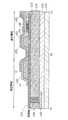
- FIG. 18is an enlarged view of the vicinity of the end of the display area of the organic EL display panel.
- FIG. 19Ais a diagram showing a configuration in which a charge functional layer is formed in common over each light emitting element.
- FIG. 19Ais a cross-sectional view of the vicinity of the edge of the display area shown in FIG. Specifically, FIG. 19A is a cross-sectional view of the vicinity of the end of the display area along the line A9-C9 in FIG.
- the line A9-C9is a line passing through the position B9 in FIG.
- the TFT layer 132Jis formed on the substrate 133J.
- a power supply wiring 110Jis provided in the TFT layer 132J.
- An interlayer insulating film 131Jis formed on the TFT layer 132J.
- An auxiliary wiring 121J and an anode electrode 122J as a pixel electrodeare formed on the interlayer insulating film 131J.
- the anode electrode 122Jis electrically connected to the TFT of the TFT layer 132J through a contact hole (not shown) formed in the interlayer insulating film 131J.
- the auxiliary wiring 121Jis electrically connected to the power supply wiring 110J by the contact plug 134J.
- a partition wall 130Jis formed above the interlayer insulating film 131J.
- the organic light emitting layer 140Jis formed in each opening formed in the partition wall 130J.
- the charge functional layer 151Jis formed over a plurality of openings formed in the partition wall 130J.
- the cathode electrode 152Jis formed on the charge functional layer 151J. That is, the cathode electrode 152J is a common electrode used in common as the anodes of a plurality of light emitting elements.
- the peripheral area of the display areais an area outside the display area and surrounding the display area.
- the peripheral area of the display areais also simply referred to as a peripheral area.
- the cathode electrode 152J as the common electrode and the auxiliary wiring 121Jare electrically connected via at least the charge functional layer 151J. Will be connected.
- the cathode electrode 152Jis directly connected to the auxiliary wiring 121J electrically connected to the power supply wiring 110J without interposing the charge functional layer 151J.
- the drain electrode of the P-type TFTis connected to the organic EL element, and the electrostatic holding capacitance is P-type. It is disposed between the source and gate electrodes of the TFT.
- the voltage of the gate electrode of the driving TFTis increased as the potential of the lower electrode of the organic EL element (anode potential) is increased from the OFF voltage of the organic EL element to the ON voltage when switching from the writing period to the light emission period. Does not occur (bootstrap phenomenon).
- the bootstrap phenomenonoccurs as follows when the anode electrode is a common electrode.
- the anode electrode that is a common electrodeis 152J '
- the cathode electrode that is a pixel electrodeis 122J'.
- FIG. 20is a diagram illustrating an example of a circuit configuration of the sub-pixel unit PX9 using a P-type TFT.
- the sub-pixel unit PX9is one sub-pixel unit among the three sub-pixel units that form one pixel unit.
- the sub-pixel unit PX9is provided with a scanning line 521, a control line 522, and a signal line 511 in association with each other.
- the sub-pixel unit PX9includes a drive transistor T1, switching transistors T2, T3, T4, a capacitor C10, a light emitting element EL9, a cathode power supply line serving as a negative power supply, and a power supply wiring serving as a positive power supply.
- the cathode power supply linesupplies a cathode voltage VEE.
- the power supply wiringsupplies the voltage VDD.
- the drive transistor T1is a P-type TFT.
- the light emitting element EL9is an organic EL element.
- FIG. 21is a timing chart for explaining the operation of the sub-pixel unit PX9.
- FIG. 21shows waveforms of voltages generated in each of the control line 522, the scanning line 521, and the signal line 511.
- FIG. 22is a diagram for explaining the operation of the sub-pixel unit PX9.
- the anode transistor (VDD)does not fluctuate in the writing period in which the potential difference is set in the capacitor C10 in the sub-pixel unit PX9 as the driving circuit, so that the driving transistor T1 is turned off. Yes (see FIGS. 21 and 22A).
- Vg (0)is the gate voltage of the drive transistor T1 immediately before the start of light emission.
- Vs (0)is the source voltage of the drive transistor T1 immediately before the start of light emission.
- Vsg (0)is a source-gate voltage of the drive transistor T1 immediately before the start of light emission.
- the cathode voltage of the organic EL elementdecreases. Based on this, the potential Vs of the other electrode of the capacitor C10 connected to the organic EL element is pushed down.
- the source-gate voltage of the drive transistor T1 immediately after the start of light emissionis Vsg shown in Equation 1.
- the pixel current i pixel of the driving transistor T1has a value represented by the following Expression 2.
- C parais a capacitance component between the source and gate electrodes of the drive transistor T1 (drive transistor T1) from all the capacitive components connected to the gate electrode of the drive transistor T1, including the parasitic capacitance C0 of the drive transistor T1. (Including the parasitic capacitance).
- C 1represents the capacitance of the capacitor C10 is a capacitance component.
- Vsg (1)is a source-gate voltage of the drive transistor T1 during light emission.
- Vs (1)is the source voltage of the drive transistor T1 during light emission.
- V T (TFT)is the threshold voltage of the drive transistor T1.
- V DDcorresponds to VDD.
- Vs (1)is a voltage obtained by subtracting the on voltage of the light emitting element EL9 corresponding to the pixel current i pixel from VDD. From Equation 2, it can be seen that the pixel current i pixel is a function of VDD. That is, in the display region, when the anode voltage (VDD) of each light emitting element EL9 varies greatly depending on the position of the pixel including the light emitting element EL9, the variation of the pixel current i pixel flowing through the light emitting element EL9 also increases ( (Refer FIG.22 (b)). In this case, the light emission amount of each light emitting element EL9 in the display region varies.
- the auxiliary wiring 121Jpasses through at least the charge functional layer 151J in the display area as the effective area.
- the anode electrode 152J ′which is a common electrode
- a contact resistanceis generated by the charge functional layer 151J.
- the auxiliary wiring 121Jis directly connected to the anode electrode 152J 'as the common electrode without the charge functional layer 151J. Therefore, contact resistance due to the charge functional layer 151J does not occur.
- the charge functional layer 151Jis interposed between the anode electrode 152J 'serving as the common electrode and the auxiliary wiring 121J, thereby causing contact resistance.
- the anode electrode 152J 'as the common electrode and the auxiliary wiring 121Jare directly connected, so that no contact resistance occurs.
- FIG. 23Ais a diagram illustrating a state of luminance (relative luminance) of the display area.
- FIG. 23Bis a diagram illustrating a state of luminance (relative luminance) along the line X1-X2 in FIG.
- the amount of current flowing between the auxiliary wiring 121J and the anode electrode 152J ′ as the common electrode in the peripheral area of the display area as the effective areais the same as the auxiliary wiring 121J and the anode electrode 152J in the display area. It means that it becomes relatively larger than the amount of current flowing between. That is, in FIG. 19B, the amount of current flowing through the current path LI2 in the peripheral region is relatively larger than the amount of current flowing through the current path LI1.
- FIG. 1is a block diagram showing a configuration of display apparatus 1000 according to Embodiment 1 of the present invention.
- the display device 1000includes a display panel 100, a scanning line driving circuit 200, and a data line driving circuit 300.
- the display panel 100is an organic EL display panel using an organic EL (Electro Luminescence) element which is an organic light emitting element. That is, the display device 1000 including the display panel 100 that is an organic EL display panel is an organic EL display device.
- organic ELElectro Luminescence
- the display panel 100is an active matrix display panel including a thin film transistor for each pixel portion.
- the display panel 100is a top emission type display panel.
- the display panel 100may be a bottom emission type display panel.
- the display panel 100includes a display area R10 for displaying an image.
- the display region R10is formed on a substrate 133 described later.
- FIG. 2is a diagram showing a configuration of the display region R10.
- the position CPis the center position of the display region R10.
- a plurality of pixel portions PX10are arranged. That is, the display panel 100 includes a plurality of pixel portions PX10. The plurality of pixel portions PX10 are arranged in a matrix. Each of the plurality of pixel units PX10 emits light according to a signal supplied from the outside.
- FIG. 3is a diagram illustrating an example of the configuration of the pixel unit PX10.
- the pixel unit PX10includes sub-pixel units PX. R, PX. G, PX. B.
- Sub-pixel unit PX. R, PX. G, PX. Bis a pixel portion that emits red, green, and blue light, respectively.
- the sub-pixel portions PXR, PXG, and PXBinclude light emitting regions LR1.1, LR1.2, and LR1.3, respectively.
- the light emitting regions LR1.1, LR1.2, and LR1.3are regions that emit red, green, and blue light, respectively.
- each of Bis also simply referred to as a sub-pixel unit PX.
- each of the light emitting regions LR1.1, LR1.2, and LR1.3is also simply referred to as a light emitting region LR1.
- the pixel unit PX10is not limited to the sub-pixel unit of the three primary colors of RGB.
- four primary colorssuch as RGBW and RGBY, and further sub-pixel units corresponding to the respective primary colors may be added.
- itmay be configured by pen tile-arranged sub-pixels arranged in a matrix as one unit cell by combining RG and BG.
- FIG. 4is a diagram illustrating a circuit configuration example of the sub-pixel unit PX.
- a scanning line 221, a control line 222, and a signal line 311are provided in association with each other in the sub-pixel unit PX.
- the subpixel unit PXincludes a driving transistor T1, switching transistors T2, T3, T4, a capacitor C10, and a light emitting element EL1.
- the driving transistor T1is a P-type thin film transistor (TFT).
- Each of the switching transistors T2, T3, T4is a P-type thin film transistor (TFT).
- TFTthin film transistor
- Each of the switching transistors T2, T3, and T4is not limited to a P-type TFT, and may be an N-type TFT.
- the light emitting element EL1is an organic EL element.
- the organic EL elementemits brighter light as the current supplied to the organic EL element itself is larger.
- the binary high voltage state and low voltage state of the signal and the signal lineare also referred to as “H level” and “L level”, respectively.
- the gate electrode, the drain electrode, and the source electrode of each transistorare also referred to as a gate, a drain, and a source, respectively.
- the gates of the switching transistors T2 and T3are electrically connected to the scanning line 221.
- One of the drain and the source of the switching transistor T2is connected to the signal line 311.
- the other of the drain and the source of the switching transistor T2is connected to the node N3.
- One of the drain and source of the switching transistor T3is connected to the power line PL3.
- Power supply line PL3supplies reference voltage Vref.
- the other of the drain and the source of the switching transistor T3is connected to the node N1.
- a capacitor C10is provided between the node N1 and the node N3.
- the gate of the switching transistor T4is connected to the control line 222.
- One of the drain and the source of the switching transistor T4is connected to the node N3.
- the other of the drain and the source of the switching transistor T4is connected to the node N2.
- the gate of the driving transistor T1is connected to the node N1.
- the drain of the drive transistor T1is connected to a power supply line PL2 that supplies a voltage VEE that is a low power supply.
- the source of the driving transistor T1is connected to the node N2.
- a parasitic capacitance C0exists between the gate electrode of the P-type driving transistor T1 and the drain electrode of the driving transistor T1.
- the cathode of the light emitting element EL1is connected to the node N2.
- the anode of the light emitting element EL1is connected to a power supply line PL1 that supplies a voltage VDD that is a high power supply.
- a scanning line 221, a control line 222, and a signal line 311are provided in association with each of the plurality of sub-pixel units PX included in the display panel 100. That is, the display panel 100 includes a plurality of scanning lines 221, a plurality of control lines 222, and a plurality of signal lines 311.
- the scanning line driving circuit 200is connected to the display panel 100 by a plurality of connectors 210.
- the scanning line driving circuit 200is connected to a plurality of scanning lines 221 and a control line 222 via a plurality of connectors 210.
- the scanning line driving circuit 200controls the plurality of scanning lines 221 and the control line 222.
- the data line driving circuit 300is connected to the display panel 100 by a plurality of connectors 310.
- the data line driving circuit 300is connected to a plurality of signal lines 311 via a plurality of connectors 310.
- the data line driver circuit 300controls the plurality of signal lines 311.
- FIG. 5is a timing chart for explaining the operation of the sub-pixel unit PX according to Embodiment 1 of the present invention.
- FIG. 5shows waveforms of voltages generated on the control line 222, the scanning line 221, and the signal line 311.
- the control line 222, the scanning line 221 and the signal line 311 corresponding to the sub-pixel unit PXare controlled as in the waveform shown in FIG. 5, so that the data voltage is written from the signal line 311 to the capacitor C10. It is.
- This data voltageis a voltage that determines the current that flows through the light emitting element EL1 during the light emission period.
- control line 222 and the scanning line 221 corresponding to the sub-pixel unit PXhave the control line 222 at the L level as shown in the waveform of FIG. 5, and the switching transistor T4 is turned on.
- a data voltageis applied between the gate and source of the driving transistor T1, and a current corresponding to the data voltage flows.
- the light emitting element EL1emits light.
- a ring-shaped power supply wiring 110is provided in the peripheral region of the display region R10.
- the peripheral region of the display region R10is a region outside the display region R10.
- the power supply wiring 110is provided inside the peripheral area of the display area R10.
- auxiliary wirings 121are arranged in a grid pattern.
- the auxiliary wiring 121is made of a conductive material.
- the plurality of auxiliary wirings 121are electrically connected to the power supply wiring 110.
- Each auxiliary wiring 121is an electrode for reducing the voltage drop of the power supply line PL1 that supplies the voltage VDD at the central portion in the display region R10.
- the auxiliary wiring 121 arranged in the peripheral region of the display region R10is not shown for the sake of simplification.
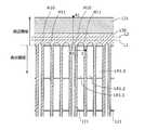
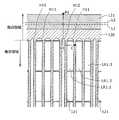
- FIG. 6Ais an enlarged view of a region R20 near the end of the display region R10. Region R20 is the region shown in FIG.
- a plurality of pixel portions PX10 arranged in the vertical directionare arranged between two adjacent auxiliary wirings 121 in the horizontal direction of FIG. 6A.
- Each pixel unit PX10includes sub pixel units PX. R, PX. G, PX. B.
- the light emitting regions LR1.1, LR1.2, and LR1.3 shown in FIG. 6Aare the light emitting regions LR1.1, LR1.2, and LR1.3 in one pixel unit PX10 shown in FIG.
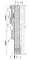
- FIG. 6Bis a partial cross-sectional view of display panel 100 according to Embodiment 1 of the present invention. Specifically, FIG. 6B is a cross-sectional view of the vicinity of the end of the display region R10 along the line A1-C1 of FIG. 6A.
- the A1-C1 lineis a line passing through the position B1 in FIG. 6A.
- componentsfor example, a resin layer, a sealing glass, etc.
- the resin layer not shownis formed of a high resistance material.
- the resin layermay be formed so as to cover a later-described anode electrode 152 and a portion where the anode electrode 152 is not formed.
- FIGS. 6A and 6Bare not a configuration that is applied only to the upper end of the display region R10 in FIG.
- the configuration near the lower end, the left end, and the right end of the display region R10is also the configuration shown in FIGS. 6A and 6B. That is, the configuration in the vicinity of the peripheral region of the display region R10 is the configuration illustrated in FIGS. 6A and 6B.
- the peripheral area of the display area R10is an area in the display area R10 and an end area of the display area R10.
- the display panel 100includes a substrate 133, a TFT layer 132, an interlayer insulating film 131, a power supply wiring 110, an auxiliary wiring 121, a cathode electrode 122, a partition wall 130, and a charge functional layer 151. And an anode electrode 152 and an organic light emitting layer 140.
- a TFT layer 132is formed on the substrate 133.
- an elementsuch as a transistor included in each pixel unit PX10 in the display region R10 is formed. That is, the TFT layer 132 includes a P-type drive transistor T1. In other words, the TFT layer 132 includes a P-type TFT as a driving TFT.
- a power supply wiring 110is formed in the TFT layer 132.
- the interlayer insulating film 131is formed on the TFT layer 132.
- the cathode electrode 122is an electrode corresponding to the cathode of the light emitting element EL1. That is, the cathode electrode 122 is a lower electrode of the light emitting element EL1.
- the cathode electrode 122is formed on the interlayer insulating film 131.
- the cathode electrode 122is provided corresponding to each sub-pixel unit PX in the display region R10. That is, a plurality of cathode electrodes 122 are disposed in the display region R10 on the interlayer insulating film 131.
- an auxiliary wiring 121is formed on the interlayer insulating film 131.
- the auxiliary wiring 121is disposed in the peripheral area of the display area R10 and in the display area R10.
- the auxiliary wiring 121 arranged in the peripheral region of the display region R10is electrically connected to the power supply wiring 110 by the contact plug 134.
- the connection between the auxiliary wiring 121 and the power supply wiring 110is not limited to a mode in which the auxiliary wiring 121 and the power supply wiring 110 are provided in different layers and are electrically connected by the contact plug 134.
- the power supply wiring 110 and the auxiliary wiring 121may be formed in the same layer. In that case, a separate member is provided to electrically connect the auxiliary wiring 121 and the power supply wiring 110.
- auxiliary wiring 121is arranged separately from the cathode electrode 122 in the display region R10. That is, the auxiliary wiring 121 is not directly connected to each cathode electrode 122.
- Each cathode electrode 122is electrically connected to the drive transistor T1 of each pixel portion PX10 of the TFT layer 132 through a contact hole (not shown) formed in the interlayer insulating film 131.
- the cathode electrode 122 and the auxiliary wiring 121may be formed in the same wiring layer on the interlayer insulating film 131.
- a partition wall 130is formed above the interlayer insulating film 131 so as to cover at least the end of the anode electrode 152.
- the partition wall 130is made of an organic material. Further, the surface of the partition wall 130 is subjected to a liquid repellent treatment.
- the liquid repellent processis, for example, a liquid repellent process using fluorine plasma or the like.
- the organic material which comprises the partition 130may have liquid repellency.
- the surface of the partition wall 130is not subjected to liquid repellency treatment, and the partition wall 130 is made of an organic material having liquid repellency.
- the organic material having liquid repellencyincludes, for example, a fluororesin.
- the fluororesin contained in the partition wall 130 (bank)is not particularly limited as long as it has fluorine atoms in at least some of the polymer repeating units. Examples of the fluororesin include fluorinated polyolefin resin, fluorinated polyimide resin, fluorinated polyacrylic resin, and the like.
- a plurality of openingsare formed in the partition wall 130.
- the plurality of openingsare openings H10 or openings H11 as shown in FIG. 6A.
- the opening H10exposes the auxiliary wiring 121 in a step before the charge functional layer 151 is formed.
- the opening H10is formed on the auxiliary wiring 121.
- the opening H11is provided in association with each sub-pixel part PX.
- the opening H11exposes the cathode electrode 122 in a step before the charge functional layer 151 and the organic light emitting layer 140 are formed.
- the opening H11is formed on the cathode electrode 122. That is, the partition wall 130 is formed with a plurality of openings formed on the cathode electrode 122 or the auxiliary wiring 121 in the display region R10.
- the anode electrode 152is a common electrode that is commonly used as the anode of each light emitting element EL1 in the display region R10.
- the anode electrode 152is formed on the charge functional layer 151 described later.
- the anode electrode 152is formed in common for each sub-pixel unit PX in the display region R10. That is, the anode electrode 152 is formed above the partition wall 130 to face the plurality of auxiliary wirings 121 and the cathode electrodes 122.
- the power supply wiring 110is a wiring for finally supplying an anode voltage (VDD) to the anode electrode 152.
- the power supply wiring 110is provided at least in the peripheral region of the display region R10. That is, the power supply wiring 110 for supplying power to the anode electrode 152 is provided in the peripheral region of the display region R10.
- the power supply wiring 110is electrically connected to the auxiliary wiring 121 arranged in the peripheral region of the display region R10 by a contact plug 134.
- the anode electrode 152is supplied with power (anode voltage (VDD)) from the power supply wiring 110 via the contact plug 134, the auxiliary wiring 121, and the charge functional layer 151 in the display region R10. That is, the anode electrode 152 is supplied with power from the power line 110 through at least the charge functional layer 151 in the display region R10. In other words, the anode electrode 152 is supplied with power from the power supply wiring 110 via at least the charge functional layer 151 in the entire region of the anode electrode 152.
- VDDanode voltage
- the auxiliary wiring 121 disposed in the peripheral region of the display region R10is below a partition wall 130 that is located near the boundary between the display region R10 and the peripheral region of the display region R10.
- a portion of the auxiliary wiring 121 located in the peripheral region of the display region R10is included in the auxiliary wiring 121 via the partition 130 located near the boundary between the display region R10 and the peripheral region of the display region R10. It is connected to a part located in the display area R10.
- the partition wall 130 positioned near the boundary between the display region R10 and the peripheral region of the display region R10is a portion of the partition wall 130 positioned near the boundary between the display region R10 and the peripheral region of the display region R10, that is, the partition wall 130. Is part of.
- auxiliary wiring 121 arranged in the peripheral region of the display region R10is not directly connected to the anode electrode 152 in the peripheral region of the display region R10.
- the anode electrode 152is connected to the auxiliary wiring 121 disposed in the display region R10 via the charge functional layer 151.
- the charge functional layer 151is formed of a high-resistance material. Therefore, a current flowing between the power supply wiring 110 and the organic light emitting layer 140 in the sub-pixel unit PX located at the peripheral portion of the display region R10 flows through the current path LI1. That is, the current needs to pass through the high-resistance charge functional layer 151.
- the wiring resistance of the auxiliary wiring 121is set to be smaller than the wiring resistance of the anode electrode 152, the main cause of the potential fluctuation of the anode electrode 152 is the wiring resistance of the auxiliary wiring 121, and the potential distribution of the anode electrode 152 is changed. It can be greatly uniformized.
- the organic light emitting layer 140is a layer mainly composed of an organic light emitting material that emits light by recombination of holes and electrons.
- the organic light emitting layer 140corresponds to a part of the light emitting element EL1.
- the organic light emitting layer 140is formed in the opening H11 corresponding to each sub-pixel unit PX.
- the organic light emitting layer 140is formed on the cathode electrode 122. That is, the organic light emitting layer 140 is formed in each of the plurality of openings H11 formed in the partition wall 130. In other words, the organic light emitting layer 140 is formed between the cathode electrode 122 and the anode electrode 152 in each opening H11 formed on the cathode electrode 122 in the partition wall 130.
- the charge functional layer 151is a layer in which a hole transport layer, a hole injection layer, or a hole transport layer and a hole injection layer are laminated in this order. That is, the charge functional layer 151 is a higher resistance material than the cathode electrode 122 and the anode electrode 152 which are conductive layers. That is, the charge functional layer 151 includes at least a hole injection layer or a hole transport layer.
- the charge functional layer 151is formed so as to cover a plurality of openings formed in the partition wall 130. That is, the charge functional layer 151 is formed so as to cover the top of the organic light emitting layer 140 corresponding to each sub-pixel unit PX in the display region R10. That is, the charge functional layer 151 is formed in common with respect to the plurality of organic light emitting layers 140 formed in the plurality of openings H11. In addition, the charge functional layer 151 is formed between the anode electrode 152 and the partition wall 130. That is, the charge functional layer 151 is formed in common with respect to each of the organic light emitting layers 140 across the plurality of openings between the anode electrode 152 and the partition wall 130.
- the source electrode of the P-type drive transistor T1is electrically connected to the cathode (cathode electrode 122) of the light emitting element EL1. That is, the source electrode of the P-type TFT (drive transistor T1) is electrically connected to the cathode electrode 122.
- a current corresponding to the voltage (Vsg) between the source electrode and the gate electrode of the P-type TFT (driving transistor T1) in the light emission period of FIG. Lightis emitted by flowing to the cathode electrode 122.
- connection resistance between the anode electrode 152 and the auxiliary wiring 121 per unit area in the central region of the display region R10is R cont (pix), and the anode electrode per unit area in the peripheral region of the display region R10.
- R contthe connection resistance between the auxiliary wiring 121 and R 152
- the resistance of the anode electrode 152is R ANO
- the resistance of the auxiliary wiring 121is R BUS
- R ANO and R BUS of Formula 3are expressed by Formula 4 and Formula 5 below, respectively.
- R ANOR ⁇ (ANO) ⁇ n (Formula 4)
- R BUSR ⁇ (BUS) ⁇ L PIX / w BUS ⁇ m (Formula 5)
- R ⁇ (ANO) in Equation 4is the sheet resistance of the anode electrode 152 as a cathode.
- the sheet resistanceis a value obtained by dividing the resistivity of the anode electrode 152 by the film thickness of the anode electrode 152.
- R ⁇ (BUS) in Equation 5is the sheet resistance of the auxiliary wiring 121.
- the sheet resistance of the auxiliary wiring 121is a value obtained by dividing the resistivity of the auxiliary wiring 121 by the film thickness of the auxiliary wiring 121.
- L PIXis a pixel pitch. That is, L PIX is a distance between two adjacent pixel portions PX10.
- w BUSis the width of the auxiliary wiring 121 in the short direction.
- the sheet resistance value of the anode electrode 152is larger than the sheet resistance value of the auxiliary wiring 121.
- FIG. 7is a diagram for explaining a part of a formula relating to the anode electrode 152 and the auxiliary wiring 121.
- FIG. 7Ais a diagram showing the configuration of the power supply wiring 110 and the auxiliary wiring 121 according to the first embodiment.
- a plurality of auxiliary wirings 121are electrically connected to the power supply wiring 110.
- the pixel portion PX10 at the upper end of the display region R10is also referred to as an upper end pixel.
- the pixel portion PX10 at the lower end of the display region R10is also referred to as a lower end pixel.
- the leftmost pixel portion PX10 of the display region R10is also referred to as a leftmost pixel.
- the rightmost pixel portion PX10 of the display region R10is also referred to as a rightmost pixel.
- the upper end pixel, the lower end pixel, the left end pixel, and the right end pixelare pixels close to the power supply wiring 110.
- a certain pixel portion PX10 in the display region R10is referred to as a pixel A.
- the number of pixels (pixel unit PX10) arranged from the pixel A to the uppermost pixel closest to the pixel Ais referred to as the upper pixel number.
- the number of pixels arranged from the pixel A to the lowermost pixel closest to the pixel Ais referred to as the lower pixel number.
- the number of pixels arranged from the pixel A to the leftmost pixel closest to the pixel Ais referred to as the left pixel number.
- the number of pixels arranged from the pixel A to the rightmost pixel closest to the pixel Ais referred to as the right pixel number.
- N in Equation 4is the smallest number (integer) among the number of upper pixels, the number of lower pixels, the number of left pixels, and the number of right pixels.
- peripheral area of the display area R10is also simply referred to as a peripheral area A.
- the peripheral area Ais an area outside the display area R10.
- the line L1indicates the position of the end of the anode electrode 152 in the peripheral region A.
- a line L2 in FIGS. 6A and 6Bindicates the position of the end of the charge functional layer 151 in the peripheral region A.
- the end of the anode electrode 152 and the end of the charge functional layer 151are located near the boundary between the display region R10 and the peripheral region of the display region R10. It is provided above the partition wall 130.
- an end portion of the charge functional layer 151is provided on the partition wall 130 located near the boundary between the display region R10 and the peripheral region of the display region R10.
- the end portion of the anode electrode 152is provided on the charge functional layer 151. That is, the end of the anode electrode 152 is provided above the partition wall 130 located near the boundary between the display region R10 and the peripheral region of the display region R10. In other words, the end of the anode electrode 152 and the end of the charge functional layer 151 are extended to above the partition wall 130 located near the boundary between the display region R10 and the peripheral region of the display region R10. Yes.
- the contact resistance by the charge functional layer 151is a resistance generated at the interface where the auxiliary wiring 121 and the charge functional layer 151 are bonded, a resistance generated at the interface where the anode electrode 152 and the charge functional layer 151 are bonded, and , The electric resistance of the charge functional layer 151.
- the wiring resistance of the auxiliary wiring 121is smaller than the wiring resistance of the anode electrode 152, the main factor of potential fluctuation of the anode electrode 152 can be the wiring resistance of the auxiliary wiring 121.
- the potential distribution of the anode electrode 152can be made substantially uniform, and the difference in the amount of current generated in the central region and the peripheral region of the display region R10 can be reduced.
- the common electrodeis an anode electrode
- the compression ratio of the potential difference set in the capacitor C10can be made substantially the same in the peripheral region and the central region of the display region R10. Thereby, the influence on display uniformity can be suppressed small. That is, it is possible to improve the voltage distribution imbalance of the anode electrode 152 as the common electrode and suppress display deterioration.
- the distance from the center of the display region R10 (position CP in FIG. 2) to the end of the anode electrode 152is shorter than the distance from the center of the display region R10 to the end of the charge functional layer 151.
- a straight line passing through the position CP in FIG. 2 on the surface of the display region R10is referred to as a straight line A.
- the distance from the position CP on the straight line A to the end of the anode electrode 152is shorter than the distance from the position CP on the straight line A to the end of the charge functional layer 151 located near the end of the anode electrode 152. That is, the distance from the center on the straight line A passing through the center (position CP) of the display region R10 to the end of the anode electrode 152 is located in the vicinity of the end of the anode electrode 152 from the center on the straight line A. Shorter than the distance to the end of the charge functional layer 151.
- the end of the anode electrode 152 on the straight line Ais located in the center (position) of the display region R10 from the end of the charge functional layer 151 on the straight line A, which is located in the vicinity of the end of the anode electrode 152. (CP).
- the parasitic capacitance C0exists between the gate electrode of the P-type drive transistor T1 and the drain electrode of the drive transistor T1. That is, a parasitic capacitance C0 exists between the gate electrode of the P-type TFT (driving transistor T1) and the drain electrode of the P-type TFT.
- the potential of the other electrode of the capacitor C10is pushed down more in the peripheral region than in the central region of the display region R10 due to the decrease in the potential of the anode voltage (VDD). Due to the presence of the parasitic capacitance C0 between the gate electrode of the P-type TFT (driving transistor T1) and the drain electrode of the P-type TFT, the depression of the potential of one electrode of the capacitor C10 is suppressed.
- the auxiliary wiring 121 arranged in the peripheral region of the display region R10is not directly connected to the anode electrode 152 in the peripheral region of the display region R10.
- the voltage of the anode electrode 152 in the peripheral region of the display region R10 and the voltage of the anode electrode 152 in the display region R10are both voltages through the charge functional layer 151 having a high resistance.
- imbalance in the voltage distribution of the anode electrode 152 as the common electrodecan be suppressed, and display deterioration can be prevented.
- connection resistance between the anode electrode 152 and the auxiliary wiring 121 per unit area in the central area of the display area R10is R cont (pix), and the unit area in the peripheral area of the display area R10.
- R contthe connection resistance between the anode electrode 152 and the auxiliary wiring 121
- the resistance of the anode electrode 152is R ANO
- the resistance of the auxiliary wiring 121is R BUS
- the current flowing through the pixelpreferentially flows through the auxiliary wiring 121 having a lower resistance than the anode electrode 152 having a high resistance. Therefore, a rapid change in the voltage drop in the peripheral region of the display region R10 due to the resistance of the anode electrode 152 is reduced, and the voltage distribution of the anode electrode 152 is made uniform. Therefore, display unevenness in the display region R10 can be reduced.
- the partition 130does not function to partition pixels unless the surface of the partition 130 that separates pixels has liquid repellency. Therefore, as described above, the partition wall 130 is made of an organic material. Further, the surface of the partition wall 130 is subjected to a liquid repellent treatment. That is, the surface of the partition wall 130 has liquid repellency.
- the minimum amount of ink overflowing from the partition wallcan be increased, and mixing of adjacent colors of inks can be prevented.
- the organic light emitting layer 140is formed by a coating method, the thickness of the applied organic light emitting layer 140 can be formed uniformly.
- the material constituting the partition wall 130may be an organic material having liquid repellency.
- the surface of the partition wall 130is not subjected to liquid repellency treatment, and the partition wall 130 is made of an organic material having liquid repellency.
- the partition wall 130is made of an organic material having liquid repellency, the minimum amount of ink overflowing from the partition wall can be increased when applying different ink types for each color. It is possible to prevent the inks from mixing and mixing colors.
- the organic light emitting layer 140is formed by a coating method, the thickness of the applied organic light emitting layer 140 can be formed uniformly.
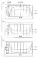
- FIG. 8is a diagram showing an example of characteristics in the display area.
- Vdrop in FIG. 8Ais a voltage fluctuation amount in the display region with respect to the display end voltage VDD0 of the anode voltage VDD. That is, the anode voltage in the display area is represented by VDD0 + Vdrop.
- the horizontal axis in FIG. 8Acorresponds to one line (hereinafter also referred to as a measurement line) in the horizontal direction (row direction) in the display region R10. Also in the vertical direction (column direction) of the display region R10, the voltage / current distribution has the same shape as in FIG.
- FIG. 8Ais a diagram showing a change in the voltage drop of each light emitting element EL1 corresponding to the measurement line.
- the display endindicates an end in the horizontal direction (row direction) of the display region R10.
- the display centercorresponds to the position CP in FIG.
- the horizontal axes in FIGS. 8B and 8Care the same as the horizontal axis in FIG.
- Characteristic line L21indicates the characteristic of the comparison technique (hereinafter, also referred to as comparison technique A) having the configuration described in FIG. 19B.
- a characteristic line L22indicates the characteristic in the configuration of the present embodiment.
- FIG. 8Bis a diagram showing the characteristics of the amount of change in the source-gate voltage Vsg of each drive transistor T1 corresponding to the measurement line.
- a characteristic line L31indicates the characteristic of the comparative technique A.
- a characteristic line L32indicates the characteristic in the configuration of the present embodiment. As shown in FIG. 8B, it can be seen that the difference in the amount of change in the source-gate voltage between the display end and the display center is smaller in the present embodiment than in the comparative technique A.
- FIG. 8Cis a diagram showing the characteristics of the current flowing through each sub-pixel unit PX corresponding to the measurement line.
- a characteristic line L41indicates the characteristic of the comparative technique A.
- a characteristic line L42indicates the characteristic in the configuration of the present embodiment. As shown in FIG. 8C, it can be seen that the amount of change in the current flowing through the sub-pixel portion at the display end and the display center is smaller in the present embodiment than in the comparison technique A.
- circuit configuration of the sub-pixel unit PXis not limited to the configuration shown in FIG.
- the circuit configuration of the sub-pixel unit PXmay be the circuit configuration illustrated in FIG.
- the circuit configuration of FIG. 9is different from the circuit configuration of FIG. 4 in that control lines 223 and 224 are further provided in association with the sub-pixel unit PX and a capacitor C20 is further provided. Note that the circuit of FIG. 9 is a circuit for compensating the threshold voltage V T of the drive transistor T1.
- the circuit shown in FIG. 9operates according to the timing chart shown in FIG.
- the configuration of the power supply wiring 110 and the auxiliary wiring 121is not limited to the configuration of FIG.
- the plurality of auxiliary wirings 121 included in the display panel 100may be arranged along only the vertical direction. Even in this configuration, the above-described Expression 3 is satisfied. In this case, if the pixel A is in the region R32 in FIG. 7B, m ⁇ n.
- the configurationmay be such that the two power supply wirings 110 are arranged so as to sandwich the two long sides of the display region R10.
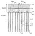
- FIG. 11is an enlarged view of a region R20 near the end of the display region R10.
- FIG. 12is a cross-sectional view of a part of the display panel 100 according to Modification 1 of Embodiment 1 of the present invention. Specifically, FIG. 12 is a cross-sectional view of the vicinity of the end of the display region R10 along the line A1-C1 of FIG. 11 and 12 indicates the position of the end of the anode electrode 152 in the peripheral region A. A line L2 in FIG. 11 and FIG. 12 indicates the position of the end of the charge functional layer 151 in the peripheral region A.
- the configuration of the anode electrode 152 and the charge functional layer 151is the same as the configuration of FIG. 6B of the first embodiment. That is, the distance from the center of the display region R10 (position CP in FIG. 2) to the end of the anode electrode 152 is shorter than the distance from the center of the display region R10 to the end of the charge functional layer 151. Specifically, as described above, the distance from the center on the straight line A passing through the center (position CP) of the display region R10 to the end of the anode electrode 152 is from the center on the straight line A to the anode electrode. It is shorter than the distance to the end of the charge functional layer 151 located near the end of 152.
- the end of the anode electrode 152is provided above the partition wall 130 located near the boundary between the display region R10 and the peripheral region of the display region R10.
- the end portion of the charge functional layer 151is extended so as to cover the entire partition wall 130 located near the boundary between the display region R10 and the peripheral region of the display region R10. That is, the end portion of the charge functional layer 151 is connected to the auxiliary wiring 121 in the peripheral region of the display region R10. Note that, in the peripheral region of the display region R10, the end portion of the anode electrode 152 is not connected to the auxiliary wiring 121.
- the same effect as that of the first embodimentcan be obtained. That is, the imbalance of the voltage distribution of the anode electrode 152 as the common electrode can be improved and display deterioration can be suppressed. In addition, the same effect can be obtained even when the portion where the charge functional layer 151 is covered with the cathode electrode 152 and the portion where it is not covered are mixed in the vicinity of the end portion of the charge functional layer 151. it can.
- FIG. 13is an enlarged view of the region R20 near the end of the display region R10.
- FIG. 14is a partial cross-sectional view of display panel 100 according to Modification 2 of Embodiment 1 of the present invention. Specifically, FIG. 14 is a cross-sectional view of the vicinity of the end of the display region R10 along the line A1-C1 of FIG. A line L1 in FIGS. 13 and 14 indicates the position of the end of the anode electrode 152 in the peripheral region of the display region R10. A line L2 in FIGS. 13 and 14 indicates the position of the end of the charge functional layer 151 in the peripheral region of the display region R10.
- the configurations of the anode electrode 152 and the charge functional layer 151are the same as the configurations of the first embodiment. That is, the distance from the center of the display region R10 (position CP in FIG. 2) to the end of the anode electrode 152 is shorter than the distance from the center of the display region R10 to the end of the charge functional layer 151. Specifically, as described above, the distance from the center on the straight line A passing through the center (position CP) of the display region R10 to the end of the anode electrode 152 is from the center on the straight line A to the anode electrode. It is shorter than the distance to the end of the charge functional layer 151 located near the end of 152.
- the end of the anode electrode 152 and the end of the charge functional layer 151are provided at the end (peripheral region) of the display region R10.
- the end portion of the anode electrode 152is not connected to the auxiliary wiring 121.
- the same effect as that of the first embodimentcan be obtained. That is, it is possible to improve the voltage distribution imbalance of the anode electrode 152 as the common electrode and suppress display deterioration. In addition, the same effect can be obtained even when the portion where the charge functional layer 151 is covered with the cathode electrode 152 and the portion where it is not covered are mixed in the vicinity of the end portion of the charge functional layer 151. it can.
- FIG. 15is an enlarged view of the region R20 near the end of the display region R10.
- FIG. 16is a cross-sectional view of a part of the display panel 100 according to the third modification of the first embodiment of the present invention. Specifically, FIG. 16 is a cross-sectional view of the vicinity of the end of the display region R10 along the line A1-C1 of FIG. A line L1 in FIGS. 15 and 16 indicates the position of the end of the anode electrode 152 in the peripheral region A. A line L2 in FIG. 15 and FIG. 16 indicates the position of the end of the charge functional layer 151 in the peripheral region A.
- the configuration of the anode electrode 152 and the charge functional layer 151is the same as the configuration of the first embodiment. That is, the distance from the center of the display region R10 (position CP in FIG. 2) to the end of the anode electrode 152 is shorter than the distance from the center of the display region R10 to the end of the charge functional layer 151. Specifically, as described above, the distance from the center on the straight line A passing through the center (position CP) of the display region R10 to the end of the anode electrode 152 is from the center on the straight line A to the anode electrode. It is shorter than the distance to the end of the charge functional layer 151 located near the end of 152.
- the end of the anode electrode 152 and the end of the charge functional layer 151are extended so as to cover the entire partition wall 130 located near the boundary between the display region R10 and the peripheral region of the display region R10. Yes.
- the same effect as that of the first embodimentcan be obtained. That is, the imbalance of the voltage distribution of the anode electrode 152 as the common electrode can be improved and display deterioration can be suppressed.
- auxiliary wiring 121 arranged in the peripheral region of the display region R10is not directly connected to the anode electrode 152 in the peripheral region of the display region R10.
- Both voltagesare voltages via the charge functional layer 151.
- an imbalance in the voltage distribution of the anode electrode 152 as the common electrodecan be suppressed, and display deterioration can be prevented.
- the same effectcan be obtained even when the portion where the charge functional layer 151 is covered with the cathode electrode 152 and the portion where it is not covered are mixed in the vicinity of the end portion of the charge functional layer 151. it can.
- FIG. 17is an external view of a display device 1000 including the display panel 100.
- the display device according to the present inventionhas been described based on the embodiments. However, the present invention is not limited to these embodiments.
- the charge functional layer 151 and the end portions of the anode electrode 152are provided.
- the positionmay be a combination of the above-described embodiment and its modifications. Unless it deviates from the meaning of this invention, the form which carried out the various deformation
- the present inventioncan be applied to any pixel configuration in which the pixel current varies due to an imbalance in the voltage distribution of the common electrode. For example, this is true even if the driving TFT is an N-type TFT. Even when the N-type TFT operates in the saturation region, the pixel current depends on the voltage between the source and drain of the driving TFT, and the non-uniform voltage distribution of the common electrode causes the voltage between the source and drain of the driving TFT to fluctuate. As a result, the pixel current becomes non-uniform. Therefore, if the uniformity of the voltage distribution of the common electrode is improved, the pixel current can be made uniform, and the display quality can be improved.
- the present inventioncan be used as an organic EL display panel and an organic EL display device that can improve imbalance in the voltage distribution of the common electrode and suppress display deterioration.
- Display panel 110110J Power supply wiring 121, 121J Auxiliary wiring 122, 122J ', 152J Cathode electrode 122J, 152, 152J' Anode electrode 130, 130J Partition 131, 131J Interlayer insulating film 132, 132J TFT layer 133, 133J Substrate 134, 134J Contact plugs 140, 140J Organic light emitting layers 151, 151J Charge functional layer 152 Anode electrode 200 Scan line drive circuit 300 Data line drive circuit 1000 Display device C0 Parasitic capacitance C10 Capacitor EL1, EL9 Light emitting elements H10, H11 Openings PX, PX. R, PX. G, PX. B, PX9 Sub-pixel portion PX10 Pixel portion R10 Display area T1 drive transistor T2, T3, T4 switching transistor
Landscapes
- Engineering & Computer Science (AREA)
- Microelectronics & Electronic Packaging (AREA)
- Electroluminescent Light Sources (AREA)
- Devices For Indicating Variable Information By Combining Individual Elements (AREA)
Abstract
Description
Translated fromJapanese本発明は、有機EL(Electro Luminescence)素子を用いた有機EL表示パネル及び有機EL表示装置に関する。The present invention relates to an organic EL display panel and an organic EL display device using an organic EL (Electro Luminescence) element.
従来、この種の有機EL表示パネル及び有機EL表示装置としては、表示パネルの大画面化に伴い、表示パネル面内の中央部分での電圧降下を防止するため補助電極を設ける構成が知られている(特許文献1の図4参照)。以下においては、特許文献1に示される技術を、従来技術Aともいう。Conventionally, as this type of organic EL display panel and organic EL display device, a configuration in which an auxiliary electrode is provided in order to prevent a voltage drop at a central portion in the display panel surface as the display panel is enlarged is known. (See FIG. 4 of Patent Document 1). Hereinafter, the technique disclosed in
この従来技術Aでは、層間絶縁膜上に画素電極としての第1電極を複数配置し、この複数の画素電極間を隔壁で区画し、この隔壁で区画された領域に発光機能層を形成している。前記隔壁によって区画されたすべての発光機能層を覆って共通電極としての第2電極が共通に形成されている。そして、前記共通電極用の電源供給源としての第2電極用電源線が有効領域の周辺領域に設けられている。In this prior art A, a plurality of first electrodes as pixel electrodes are arranged on an interlayer insulating film, the plurality of pixel electrodes are partitioned by partition walls, and a light emitting functional layer is formed in a region partitioned by the partition walls. Yes. A second electrode as a common electrode is formed in common so as to cover all the light emitting functional layers partitioned by the partition walls. A second electrode power supply line as a power supply source for the common electrode is provided in a peripheral region of the effective region.
上述した補助電極は、前記層間絶縁膜上であって、画素電極間に設けられている。補助電極は、有効領域内では、前記第2電極と電気的に接続されている。これにより、前記補助電極を介して前記第2電極に電源供給がなされ、有効領域内の電圧降下を防いでいる。The auxiliary electrode described above is provided between the pixel electrodes on the interlayer insulating film. The auxiliary electrode is electrically connected to the second electrode in the effective region. As a result, power is supplied to the second electrode via the auxiliary electrode, and a voltage drop in the effective region is prevented.
尚、従来技術Aには、発光素子を駆動する駆動TFT(Thin Film Transistor)として、P型のTFTが開示されている(特許文献1の図2、段落0018参照)。Note that, in the prior art A, a P-type TFT is disclosed as a drive TFT (Thin Film Transistor) for driving a light emitting element (see FIG. 2, paragraph 0018 of Patent Document 1).
しかし、上記従来技術Aでは、以下のような問題が生じていた。However, the conventional technique A has the following problems.
即ち、上記従来技術Aにおいて、前記発光機能層は、有機EL物質(有機発光層)、正孔注入層、正孔輸送層、電子輸送層、電子注入層、正孔ブロック層及び電子ブロック層の一部又は全部を含むものであるが、発光素子毎にパターニングされた構成である。そのため、前記発光機能層に含まれる各層毎にパターニングする工程が必要であり、そのための設備が必要となって、製造工程が複雑でコスト高を招来していた。That is, in the related art A, the light emitting functional layer is composed of an organic EL material (organic light emitting layer), a hole injection layer, a hole transport layer, an electron transport layer, an electron injection layer, a hole block layer, and an electron block layer. Although it includes part or all, it is a structure patterned for each light emitting element. For this reason, a patterning process is required for each layer included in the light emitting functional layer, and equipment for the patterning process is required, resulting in a complicated manufacturing process and high cost.
また、有効領域(表示領域)において発光素子の共通電極の電圧分布の不均衡が生じることで、表示の不均一(表示劣化)が発生するという問題があった。In addition, there is a problem in that display unevenness (display deterioration) occurs due to an imbalance in the voltage distribution of the common electrode of the light emitting element in the effective region (display region).
そこで、本発明は、上記課題に鑑みてなされたものであって、共通電極の電圧分布の不均衡を改善し、表示劣化を抑制できる有機EL表示パネル及び有機EL表示装置を提供することを目的とする。Therefore, the present invention has been made in view of the above problems, and an object of the present invention is to provide an organic EL display panel and an organic EL display device that can improve imbalance in the voltage distribution of the common electrode and suppress display deterioration. And
上記課題を解決するためには、本発明の一態様に係る有機EL表示パネルは、基板上の表示領域内に複数配置された陰極電極と、前記表示領域の周辺領域及び前記表示領域内に配置され且つ前記表示領域内では前記陰極電極と分離して配置された補助配線と、前記表示領域において前記陰極電極又は前記補助配線上に形成された開口部が複数形成された隔壁と、前記隔壁の上方において、複数の前記陰極電極に対向して形成された陽極電極と、前記隔壁における前記陰極電極上に形成された各前記開口部内であって前記陽極電極と前記陰極電極との間に形成された有機発光層と、前記陽極電極と前記隔壁との間において、前記複数の開口部に亘って各前記有機発光層に対して共通して形成された電荷機能層と、前記周辺領域に設けられ、前記陽極電極に電源供給するための電源配線と、を具備し、前記表示領域の中央から前記陽極電極の端までの距離は、前記表示領域の中央から前記電荷機能層の端までの距離より短く、前記陽極電極は、少なくとも前記電荷機能層を介して前記電源配線から電源供給を受ける。In order to solve the above problems, an organic EL display panel according to an aspect of the present invention includes a plurality of cathode electrodes arranged in a display region on a substrate, a peripheral region of the display region, and a display region. And an auxiliary wiring arranged separately from the cathode electrode in the display region, a partition wall formed with a plurality of openings formed on the cathode electrode or the auxiliary wiring in the display region, and a partition wall Above, a plurality of anode electrodes formed to face the cathode electrodes, and formed in the openings formed on the cathode electrodes in the partition and between the anode electrodes and the cathode electrodes. An organic light emitting layer, a charge functional layer formed in common to each organic light emitting layer across the plurality of openings between the anode electrode and the partition, and provided in the peripheral region. ,in front Power supply wiring for supplying power to the anode electrode, the distance from the center of the display region to the end of the anode electrode is shorter than the distance from the center of the display region to the end of the charge functional layer, The anode electrode receives power supply from the power supply wiring through at least the charge functional layer.
本発明により、共通電極の電圧分布の不均衡を改善し、表示劣化を抑制できる。According to the present invention, the voltage distribution imbalance of the common electrode can be improved and display deterioration can be suppressed.
P型TFTを有機発光素子の駆動TFTとして用い、P型TFTのソース電極が、前記有機発光素子に含まれる陰極電極と電気的に接続されている。また、前記有機発光素子に含まれる有機発光層は、発光期間において前記P型TFTの前記ソース電極と前記ゲート電極との間の電圧に応じた電流が前記陽極電極から陰極電極に流れることにより発光する。A P-type TFT is used as a driving TFT of an organic light-emitting element, and a source electrode of the P-type TFT is electrically connected to a cathode electrode included in the organic light-emitting element. The organic light emitting layer included in the organic light emitting element emits light when a current corresponding to a voltage between the source electrode and the gate electrode of the P-type TFT flows from the anode electrode to the cathode electrode during the light emission period. To do.
ここで、画素としての駆動回路内のコンデンサに電位差を設定する書込期間から、前記コンデンサに設定された電位差に応じた電流に基づいて前記有機発光層を発光させるための発光期間に移行すると、陽極電位が下降する。これに基づき、前記コンデンサの他方の電極の電位が押し下げられる。一方で、前記P型TFTのゲート電極と前記P型TFTのドレイン電極との間の寄生容量の存在により、前記コンデンサの一方の電極の電位の押し下げは抑制される。その結果、書込期間から発光期間への移行により、コンデンサに設定された電位差が圧縮されるという現象が生ずる。Here, when a transition is made from a writing period in which a potential difference is set to a capacitor in a driving circuit as a pixel to a light emitting period for causing the organic light emitting layer to emit light based on a current corresponding to the potential difference set in the capacitor, The anode potential drops. Based on this, the potential of the other electrode of the capacitor is pushed down. On the other hand, due to the presence of the parasitic capacitance between the gate electrode of the P-type TFT and the drain electrode of the P-type TFT, the depression of the potential of one electrode of the capacitor is suppressed. As a result, a phenomenon occurs in which the potential difference set in the capacitor is compressed by the transition from the writing period to the light emission period.
陽極電圧(VDD)の下降が表示領域内で均一であれば、表示領域内の各コンデンサに設定された電位差の圧縮率も同程度になるので、表示バラツキへの影響は小さい。If the decrease in the anode voltage (VDD) is uniform within the display area, the compression ratio of the potential difference set for each capacitor in the display area will be approximately the same, so the influence on display variation is small.
しかし、上記のように、表示領域内では、共通電極としての陽極電極と補助配線との間に少なくとも電荷機能層が介在するためコンタクト抵抗が生ずる。一方、表示領域の周辺領域において、陽極電極と補助配線とが直接接続されコンタクト抵抗が生じない構成では、陽極電圧(VDD)の下降率は、表示領域の中央領域の方が、表示領域の周縁領域より高くなる。However, as described above, in the display region, contact resistance occurs because at least the charge functional layer is interposed between the anode electrode as the common electrode and the auxiliary wiring. On the other hand, in the configuration in which the anode electrode and the auxiliary wiring are directly connected in the peripheral region of the display region and no contact resistance is generated, the rate of decrease of the anode voltage (VDD) is lower in the central region of the display region. Be higher than the area.
そのため、前記有機発光層の陽極電位の下降する量は、陽極電圧(VDD)に依存する。これにより、陽極電圧(VDD)の下降率が周縁領域より高い中央領域では、前記P型TFTのゲート電極すなわち前記コンデンサの一方の電極の電位の押し下げ量も大きくなり、コンデンサに設定された電位差の圧縮率も、中央領域の方が周縁領域より高くなる。従って、周縁領域と中央領域との前記コンデンサは、書込期間において同じ電圧を保持していたとしても、発光期間において保持された電圧が異なってしまう。Therefore, the amount by which the anode potential of the organic light emitting layer decreases depends on the anode voltage (VDD). As a result, in the central region where the rate of decrease of the anode voltage (VDD) is higher than the peripheral region, the amount of the potential of the gate electrode of the P-type TFT, that is, the one electrode of the capacitor is increased, and the potential difference set in the capacitor is reduced. The compression rate is also higher in the central region than in the peripheral region. Therefore, even if the capacitors in the peripheral region and the central region hold the same voltage in the writing period, the voltages held in the light emitting period are different.
そこで、本発明の一態様に係る有機EL表示パネルは、基板上の表示領域内に複数配置された陰極電極と、前記表示領域の周辺領域及び前記表示領域内に配置され且つ前記表示領域内では前記陰極電極と分離して配置された補助配線と、前記表示領域において前記陰極電極又は前記補助配線上に形成された開口部が複数形成された隔壁と、前記隔壁の上方において、複数の前記陰極電極に対向して形成された陽極電極と、前記隔壁における前記陰極電極上に形成された各前記開口部内であって前記陽極電極と前記陰極電極との間に形成された有機発光層と、前記陽極電極と前記隔壁との間において、前記複数の開口部に亘って各前記有機発光層に対して共通して形成された電荷機能層と、前記周辺領域に設けられ、前記陽極電極に電源供給するための電源配線と、を具備し、前記表示領域の中央から前記陽極電極の端までの距離は、前記表示領域の中央から前記電荷機能層の端までの距離より短く、前記陽極電極は、少なくとも前記電荷機能層を介して前記電源配線から電源供給を受ける。Therefore, an organic EL display panel according to an aspect of the present invention includes a plurality of cathode electrodes arranged in a display region on a substrate, a peripheral region of the display region, and a display region in the display region. Auxiliary wiring arranged separately from the cathode electrode, a partition wall formed with a plurality of openings formed on the cathode electrode or the auxiliary wiring in the display region, and a plurality of the cathodes above the partition wall An anode electrode formed to face the electrode, an organic light emitting layer formed between the anode electrode and the cathode electrode in each of the openings formed on the cathode electrode in the partition; Between the anode electrode and the partition wall, the charge functional layer formed in common to each of the organic light emitting layers over the plurality of openings, and provided in the peripheral region, and supplies power to the anode electrode A distance from the center of the display region to the end of the anode electrode is shorter than a distance from the center of the display region to the end of the charge functional layer, the anode electrode, Power is supplied from the power supply wiring through at least the charge functional layer.
すなわち、本発明の一態様に係る有機EL表示パネルでは、共通電極を陽極電極とした場合、前記表示領域の中央から前記陽極電極の端までの距離は、前記表示領域の中央から前記電荷機能層の端までの距離より短く、前記陽極電極は、少なくとも前記電荷機能層を介して前記電源配線から電源供給を受けるようにした。That is, in the organic EL display panel according to one aspect of the present invention, when the common electrode is an anode electrode, the distance from the center of the display region to the end of the anode electrode is from the center of the display region to the charge functional layer. The anode electrode is supplied with power from the power supply wiring through at least the charge functional layer.
これにより、表示領域の周辺領域において陽極電極と補助配線とが直接接続される領域を無くすことができる。そのため、前記表示領域の周辺領域において、前記電荷機能層を介さないで前記陽極電極と前記補助配線との間を電流が流れることがなくなる。即ち、前記陽極電極と前記補助配線との間を流れる電流は、前記電荷機能層によるコンタクト抵抗を介することになる。従って、表示領域の中央領域と周縁領域とで各画素から補助配線への電流経路を画一化することができ、表示領域の中央領域及び周縁領域で生じる陽極電圧(VDD)の電位差をより均一化できる。Thereby, it is possible to eliminate a region where the anode electrode and the auxiliary wiring are directly connected in the peripheral region of the display region. Therefore, no current flows between the anode electrode and the auxiliary wiring without passing through the charge functional layer in the peripheral region of the display region. That is, the current flowing between the anode electrode and the auxiliary wiring is via the contact resistance by the charge functional layer. Therefore, the current path from each pixel to the auxiliary wiring can be made uniform between the central region and the peripheral region of the display region, and the potential difference of the anode voltage (VDD) generated in the central region and the peripheral region of the display region is more uniform. Can be
その結果、共通電極を陽極電極とした場合においても、共通電極としての陽極電極の電圧分布の不均衡を改善することができる。そのため、書込期間から発光期間への移行による、コンデンサに設定された電位差の圧縮率を、表示領域域において均一化させ表示劣化を抑制することができる。As a result, even when the common electrode is an anode electrode, the voltage distribution imbalance of the anode electrode as the common electrode can be improved. For this reason, the compression ratio of the potential difference set in the capacitor due to the transition from the writing period to the light emission period can be made uniform in the display area region, and display deterioration can be suppressed.
また、本発明の一態様に係る有機EL表示パネルにおいて、前記電源配線は、前記表示領域の周辺領域に配置された前記補助配線と電気的に接続され、前記表示領域の周辺領域に配置された前記補助配線は、前記表示領域と前記表示領域の周辺領域との境界付近に位置する前記隔壁の下方を介して前記表示領域内に配置された前記補助配線と接続され、前記陽極電極は、前記電荷機能層を介して前記表示領域内に配置された前記補助配線と接続される、としてもよい。Further, in the organic EL display panel according to one aspect of the present invention, the power supply wiring is electrically connected to the auxiliary wiring arranged in the peripheral area of the display area and arranged in the peripheral area of the display area. The auxiliary wiring is connected to the auxiliary wiring disposed in the display area via a lower part of the partition located near the boundary between the display area and the peripheral area of the display area, and the anode electrode It may be connected to the auxiliary wiring arranged in the display region via a charge functional layer.
また、本発明の一態様に係る有機EL表示パネルは、さらに、駆動TFTとしてのP型TFTを含むTFT層と、前記TFT層上に形成された層間絶縁膜と、を具備し、前記陰極電極は、前記層間絶縁膜上に形成され、前記P型TFTのソース電極は、前記陰極電極と電気的に接続され、前記有機発光層は、発光期間において前記P型TFTのゲート電極と前記ソース電極との間の電圧に応じた電流が前記陽極電極から前記陰極電極に流れることにより発光する。The organic EL display panel according to an aspect of the present invention further includes a TFT layer including a P-type TFT as a driving TFT, and an interlayer insulating film formed on the TFT layer, and the cathode electrode Is formed on the interlayer insulating film, the source electrode of the P-type TFT is electrically connected to the cathode electrode, and the organic light-emitting layer is formed of the gate electrode and the source electrode of the P-type TFT during the light emission period. When a current corresponding to the voltage between and flows from the anode electrode to the cathode electrode, light is emitted.
これにより、有機発光素子の駆動TFTとしてP型TFTを用いた場合であって、かつ、共通電極を陽極電極とした場合においても、共通電極としての陽極電極の電圧分布の不均衡を改善することができる。そのため、書込期間から発光期間への移行による、コンデンサに設定された電位差の圧縮率を、表示領域域において均一化させ表示劣化を抑制することができる。Thereby, even when a P-type TFT is used as the driving TFT of the organic light emitting device and the common electrode is an anode electrode, the voltage distribution imbalance of the anode electrode as the common electrode is improved. Can do. For this reason, the compression ratio of the potential difference set in the capacitor due to the transition from the writing period to the light emission period can be made uniform in the display area region, and display deterioration can be suppressed.
また、本発明の一態様に係る有機EL表示パネルにおいて、前記P型TFTの前記ゲート電極と前記P型TFTのドレイン電極との間には寄生容量が存在する、としてもよい。In the organic EL display panel according to one embodiment of the present invention, a parasitic capacitance may exist between the gate electrode of the P-type TFT and the drain electrode of the P-type TFT.
前記書込期間から前記発光期間に移行した場合、陽極電圧(VDD)の電位の下降により前記コンデンサの他方の電極の電位が、表示領域の中央領域よりも周縁領域において、より押し下げられる。一方で、前記P型TFTの前記ゲート電極と前記P型TFTのドレイン電極との間の寄生容量の存在により、前記コンデンサの一方の電極の電位の押し下げは抑制される。When the writing period shifts to the light emission period, the potential of the other electrode of the capacitor is pushed down more in the peripheral region than in the central region of the display region due to the decrease in the potential of the anode voltage (VDD). On the other hand, due to the presence of the parasitic capacitance between the gate electrode of the P-type TFT and the drain electrode of the P-type TFT, the depression of the potential of one electrode of the capacitor is suppressed.
その結果、書込期間から発光期間への移行により、コンデンサに設定された電位差が圧縮されるという現象が生ずる。As a result, a phenomenon occurs in which the potential difference set in the capacitor is compressed by the transition from the writing period to the light emission period.
また、本発明の一態様に係る有機EL表示パネルにおいて、前記表示領域の周辺領域に配置された前記補助配線は、前記表示領域の周辺領域では前記陽極電極と直接接続されていない、としてもよい。In the organic EL display panel according to one aspect of the present invention, the auxiliary wiring arranged in the peripheral region of the display region may not be directly connected to the anode electrode in the peripheral region of the display region. .
本態様によると、前記表示領域の周辺領域に配置された補助配線は、前記表示領域の周辺領域では前記陽極電極と直接接続されていない。According to this aspect, the auxiliary wiring arranged in the peripheral area of the display area is not directly connected to the anode electrode in the peripheral area of the display area.
そのため、前記表示領域の周辺領域において前記陽極電極の電圧と、前記表示領域における前記陽極電極の電圧とは、共に前記補助配線に設定された電圧に対応して前記電荷機能層を介した電圧となる。その結果、前記共通電極としての陽極電極の電圧分布の不均衡を抑制し、表示劣化を防止できる。Therefore, the voltage of the anode electrode in the peripheral region of the display region and the voltage of the anode electrode in the display region are both voltages via the charge functional layer corresponding to the voltage set in the auxiliary wiring. Become. As a result, an imbalance in the voltage distribution of the anode electrode as the common electrode can be suppressed, and display deterioration can be prevented.
また、本発明の一態様に係る有機EL表示パネルにおいて、前記表示領域の中央領域における単位面積当たりの前記陽極電極と前記補助配線との接続抵抗をRcont(pix)とし、前記表示領域の周縁領域における単位面積当たりの前記陽極電極と前記補助配線との接続抵抗をRcont(EDGE)とし、前記陽極電極の抵抗をRANOとし、前記補助配線の抵抗をRBUSとした場合、Rcont(EDGE)+RANO≧Rcont(pix)+RBUSなる関係式が満たされる、としてもよい。In the organic EL display panel according to one aspect of the present invention, the connection resistance between the anode electrode and the auxiliary wiring per unit area in the central region of the display region is Rcont (pix), and the periphery of the display region When the connection resistance between the anode electrode and the auxiliary wiring per unit area in the region is Rcont (EDGE) , the resistance of the anode electrode is RANO, and the resistance of the auxiliary wiring is RBUS( Rcont ( EDGE) + RANO ≧ Rcont (pix) + RBUS may be satisfied.
これにより、表示領域内のうち、画素に流れる電流が、高抵抗である前記陽極電極よりも低抵抗である前記補助配線に優先的に流れる。そのため、抵抗による電圧降下量を低減し、前記陽極電極の電圧分布が均一化される。よって、表示領域内での表示ムラを低減できる。Thereby, in the display area, the current flowing through the pixel preferentially flows through the auxiliary wiring having a lower resistance than the anode electrode having a high resistance. Therefore, the amount of voltage drop due to resistance is reduced, and the voltage distribution of the anode electrode is made uniform. Therefore, display unevenness in the display area can be reduced.
また、本発明の一態様に係る有機EL表示パネルにおいて、前記陰極電極と前記補助配線とは、前記層間絶縁膜上の同一配線層において形成されている、としてもよい。In the organic EL display panel according to an aspect of the present invention, the cathode electrode and the auxiliary wiring may be formed in the same wiring layer on the interlayer insulating film.
また、本発明の一態様に係る有機EL表示パネルにおいて、前記陽極電極の端部及び前記電荷機能層の端部は、前記表示領域と前記表示領域の周辺領域との境界付近に位置する前記隔壁の上方まで延設されている、としてもよい。Further, in the organic EL display panel according to one aspect of the present invention, the partition wall is located near the boundary between the display region and the peripheral region of the display region, the end of the anode electrode and the end of the charge functional layer It is good also as extending to above.
また、本発明の一態様に係る有機EL表示パネルにおいて、前記電荷機能層は、少なくとも正孔注入層又は正孔輸送層からなる、としてもよい。In the organic EL display panel according to one aspect of the present invention, the charge functional layer may be composed of at least a hole injection layer or a hole transport layer.
また、本発明の一態様に係る有機EL表示パネルにおいて、前記隔壁は、有機材料により構成され、前記隔壁の表面は撥液処理がなされている、としてもよい。In the organic EL display panel according to one aspect of the present invention, the partition may be made of an organic material, and the surface of the partition may be subjected to a liquid repellent treatment.
また、本発明の一態様に係る有機EL表示パネルにおいて、前記隔壁は、撥液性を有する有機材料により構成されている、としてもよい。In the organic EL display panel according to one aspect of the present invention, the partition may be made of an organic material having liquid repellency.
前記有機発光層を塗布方式により形成する場合、画素を区分けする前記隔壁の表面は撥液性を有しなければ、前記隔壁は画素を区分けする機能を果たさない。そのため、前記隔壁は、撥液性を有する有機材料により構成されている。When the organic light emitting layer is formed by a coating method, if the surface of the partition wall that separates pixels does not have liquid repellency, the partition wall does not function to separate pixels. Therefore, the said partition is comprised with the organic material which has liquid repellency.
本発明の一態様に係る有機EL表示装置は、前記有機EL表示パネルを備える。An organic EL display device according to an aspect of the present invention includes the organic EL display panel.
なお、この本発明の他の一態様に係る有機EL表示パネルについては、上記本発明の一態様に係る有機EL表示パネルの好ましい例を適用することができ、本発明の他の一態様に係る有機EL表示パネルと好ましい例とは適宜組み合わせることができる。In addition, about the organic EL display panel which concerns on this one aspect | mode of this invention, the preferable example of the organic EL display panel which concerns on one aspect | mode of the said invention can be applied, and it concerns on the other one aspect | mode of this invention. The organic EL display panel and preferred examples can be appropriately combined.
(本発明に至った経緯)
本発明の実施の形態の説明に先立ち、本発明に至った経緯及び本発明が解決しようとする課題について詳細に説明する。(Background to the present invention)
Prior to the description of the embodiments of the present invention, the background to the present invention and the problems to be solved by the present invention will be described in detail.
上述のとおり、上記従来技術Aにおいて、前記発光機能層は、有機EL物質(有機発光層)、正孔注入層、正孔輸送層、電子輸送層、電子注入層、正孔ブロック層及び電子ブロック層の一部又は全部を含むものであるが、発光素子毎にパターニングされた構成である。そのため、前記発光機能層に含まれる各層毎にパターニングする工程が必要であり、そのための設備が必要となって、製造工程が複雑でコスト高を招来していた。As described above, in the related art A, the light emitting functional layer includes an organic EL material (organic light emitting layer), a hole injection layer, a hole transport layer, an electron transport layer, an electron injection layer, a hole block layer, and an electron block. Although part or all of the layer is included, the light-emitting element is patterned. For this reason, a patterning process is required for each layer included in the light emitting functional layer, and equipment for the patterning process is required, resulting in a complicated manufacturing process and high cost.
仮に、発光機能層に含まれる、例えば、正孔注入層及び正孔輸送層の少なくとも一方から構成される電荷機能層を、各発光素子にわたって共通で形成するとした場合、発光素子毎に電荷機能層をパターニングする工程を省くことができ、製造工程を簡略化し、コスト低減を図ることができる。If the charge functional layer comprised of at least one of a hole injection layer and a hole transport layer, for example, included in the light emitting functional layer is formed in common over each light emitting element, the charge functional layer for each light emitting element. The process of patterning can be omitted, the manufacturing process can be simplified, and the cost can be reduced.
図18は、有機EL表示パネルの表示領域の端部付近を拡大した図である。FIG. 18 is an enlarged view of the vicinity of the end of the display area of the organic EL display panel.
図19Aは、電荷機能層を各発光素子にわたって共通して形成した構成を示す図である。図19Aは、図18に示される表示領域の端部付近の断面図である。具体的には、図19Aは、図18のA9-C9線に沿った、表示領域の端部付近の断面図である。A9-C9線は、図18のB9の位置を経由する線である。FIG. 19A is a diagram showing a configuration in which a charge functional layer is formed in common over each light emitting element. FIG. 19A is a cross-sectional view of the vicinity of the edge of the display area shown in FIG. Specifically, FIG. 19A is a cross-sectional view of the vicinity of the end of the display area along the line A9-C9 in FIG. The line A9-C9 is a line passing through the position B9 in FIG.
図19Aにおいて、基板133J上には、TFT層132Jが形成される。TFT層132J内には、電源配線110Jが設けられている。TFT層132J上には、層間絶縁膜131Jが形成される。層間絶縁膜131J上には、補助配線121Jと、画素電極としての陽極電極122Jとが形成される。この陽極電極122Jは、層間絶縁膜131Jに形成されるコンタクトホール(図示しない)を介してTFT層132JのTFTと電気的に接続される。補助配線121Jは、コンタクトプラグ134Jにより、電源配線110Jと電気的に接続される。In FIG. 19A, the
また、層間絶縁膜131Jの上方には、隔壁130Jが形成される。有効領域としての表示領域において、隔壁130Jに形成された各開口部内には、有機発光層140Jが形成される。In addition, a
電荷機能層151Jは、隔壁130Jに形成された複数の開口部に亘って形成される。陰極電極152Jは、電荷機能層151J上に形成される。すなわち、陰極電極152Jは、複数の発光素子のアノードとして共通して使用される共通電極である。The charge
図18の線L11は、表示領域の周辺領域における、陰極電極152Jの端の位置を示す。図18の線L12は、表示領域の周辺領域における、電荷機能層151Jの端の位置を示す。本明細書において、表示領域の周辺領域とは、表示領域外の領域であって、かつ、表示領域の周辺の領域である。以下においては、表示領域の周辺領域を、単に、周辺領域ともいう。18 indicates the position of the end of the
しかし、図19Aのような構成を想定した場合、有効領域としての表示領域内では、前記共通電極としての陰極電極152Jと前記補助配線121Jとは、少なくとも前記電荷機能層151Jを介して電気的に接続されることになる。一方、周辺領域では、前記陰極電極152Jは、電源配線110Jに電気的に接続される補助配線121Jと、前記電荷機能層151Jを介在することなく、直接接続されることになる。However, assuming the configuration as shown in FIG. 19A, in the display area as the effective area, the
この場合であっても、上記従来技術Aでは、発光素子を駆動する駆動TFTとして、P型のTFTを用いている場合は、問題は生じない。Even in this case, in the above-described prior art A, there is no problem when a P-type TFT is used as the driving TFT for driving the light emitting element.
即ち、P型TFTを駆動TFTとした用いた場合であって、かつ、陰極電極152Jが共通電極である場合、P型TFTのドレイン電極が有機EL素子に接続され、静電保持容量はP型TFTのソース・ゲート電極間に配置される。この場合、書込期間から発光期間への切替えに際して有機EL素子の下部電極の電位(アノードの電位)が有機EL素子のオフ電圧からオン電圧へと押し上げられるに伴い、駆動TFTのゲート電極の電圧が連動して押し上げられるという現象(ブートストラップ現象)が生じない。That is, when the P-type TFT is used as a driving TFT and the
そのため、書込期間から発光期間への切替えに際して陽極電極122Jにおいて電圧変動が生じても、P型TFTのゲート電極の電圧が変動せず、有機EL素子に流れる電流に変動はない。Therefore, even if voltage fluctuation occurs in the
しかし、発光素子を駆動する駆動TFTとして、P型のTFTを用いた場合であっても、陽極電極が共通電極である場合には、以下のようにブートストラップ現象が生ずる。ここで、従来技術Aの発光素子の極性を反転させた場合について説明する。また、以下説明のため、図19Bにおいて、共通電極である陽極電極を152J’とし、画素電極である陰極電極を122J’とする。However, even when a P-type TFT is used as the driving TFT for driving the light emitting element, the bootstrap phenomenon occurs as follows when the anode electrode is a common electrode. Here, the case where the polarity of the light emitting element of the prior art A is reversed will be described. For the following description, in FIG. 19B, the anode electrode that is a common electrode is 152J ', and the cathode electrode that is a pixel electrode is 122J'.
図20は、P型のTFTを用いたサブ画素部PX9の回路構成の一例を示す図である。サブ画素部PX9は、1つの画素部を構成する3つのサブ画素部のうちの1つのサブ画素部である。FIG. 20 is a diagram illustrating an example of a circuit configuration of the sub-pixel unit PX9 using a P-type TFT. The sub-pixel unit PX9 is one sub-pixel unit among the three sub-pixel units that form one pixel unit.
図20に示すように、サブ画素部PX9には、走査線521と、制御線522と、信号線511とが対応づけて設けられる。As shown in FIG. 20, the sub-pixel unit PX9 is provided with a
サブ画素部PX9は、駆動トランジスタT1と、スイッチングトランジスタT2,T3,T4と、コンデンサC10と、発光素子EL9と、負側電源となる陰極電源線と、正側電源となる電源配線とを含む。当該陰極電源線は、陰極電圧VEEを供給する。当該電源配線は、電圧VDDを供給する。The sub-pixel unit PX9 includes a drive transistor T1, switching transistors T2, T3, T4, a capacitor C10, a light emitting element EL9, a cathode power supply line serving as a negative power supply, and a power supply wiring serving as a positive power supply. The cathode power supply line supplies a cathode voltage VEE. The power supply wiring supplies the voltage VDD.
駆動トランジスタT1は、P型のTFTである。発光素子EL9は、有機EL素子である。The drive transistor T1 is a P-type TFT. The light emitting element EL9 is an organic EL element.
図21は、サブ画素部PX9の動作を説明するためのタイミングチャートである。図21は、制御線522、走査線521及び信号線511の各々で発生する電圧の波形を示す。FIG. 21 is a timing chart for explaining the operation of the sub-pixel unit PX9. FIG. 21 shows waveforms of voltages generated in each of the control line 522, the
図22は、サブ画素部PX9の動作を説明するための図である。FIG. 22 is a diagram for explaining the operation of the sub-pixel unit PX9.
図20~図22を参照して、駆動回路としてのサブ画素部PX9内のコンデンサC10に電位差を設定する書込期間においては、陽極電圧(VDD)が変動しないため、駆動トランジスタT1はオフ状態にある(図21、図22(a)参照)。Referring to FIGS. 20 to 22, the anode transistor (VDD) does not fluctuate in the writing period in which the potential difference is set in the capacitor C10 in the sub-pixel unit PX9 as the driving circuit, so that the driving transistor T1 is turned off. Yes (see FIGS. 21 and 22A).
図22(a)において、Vg(0)は、発光開始直前の駆動トランジスタT1のゲート電圧である。Vs(0)は、発光開始直前の駆動トランジスタT1のソース電圧である。Vsg(0)は、発光開始直前の駆動トランジスタT1のソース-ゲート間電圧である。22A, Vg (0) is the gate voltage of the drive transistor T1 immediately before the start of light emission. Vs (0) is the source voltage of the drive transistor T1 immediately before the start of light emission. Vsg (0) is a source-gate voltage of the drive transistor T1 immediately before the start of light emission.
前記コンデンサC10に設定された電位差に応じた電流に基づいて前記有機発光層140Jを発光させる発光期間に移行すると、有機EL素子のカソード電圧が下降する。これに基づき、有機EL素子に接続される前記コンデンサC10の他方の電極の電位Vsが押し下げられる。When the light emitting period for causing the organic
この場合、発光開始直後の駆動トランジスタT1のソース-ゲート間電圧は、式1に示されるVsgとなる。また、駆動トランジスタT1の画素電流ipixelは、以下の式2に示される値となる。In this case, the source-gate voltage of the drive transistor T1 immediately after the start of light emission is Vsg shown in

式1において、Cparaは、駆動トランジスタT1の寄生容量C0を含む、駆動トランジスタT1のゲート電極に接続された全ての容量成分から、駆動トランジスタT1のソース・ゲート電極間の容量成分(駆動トランジスタT1の寄生容量を含む)を除いた値である。C1は、容量成分であるコンデンサC10の容量を示す。Vsg(1)は、発光時における駆動トランジスタT1のソース-ゲート間電圧である。Vs(1)は、発光時における駆動トランジスタT1のソース電圧である。In

図22(b)及び式2において、VT(TFT)は、駆動トランジスタT1の閾値電圧である。また、VDDは、VDDに相当する。Vs(1)は画素電流ipixelに応じた発光素子EL9のオン電圧をVDDから減算した電圧である。式2により、画素電流ipixelはVDDの関数であることが分かる。すなわち、表示領域内において、各発光素子EL9の陽極電圧(VDD)が、当該発光素子EL9を含む画素の位置によって大きく変動する場合、当該発光素子EL9に流れる画素電流ipixelの変動も大きくなる(図22(b)参照)。この場合、表示領域内の各発光素子EL9の発光量にばらつきが生じる。In FIG. 22B and
一方で、駆動トランジスタT1のゲート電極と駆動トランジスタT1のドレイン電極との間の寄生容量C0を含む、駆動トランジスタT1のゲート電極に接続された容量成分の存在により、駆動トランジスタT1のゲート電極に接続される前記コンデンサC10の一方の電極の電位の押し下げは抑制される。その結果、書込期間から発光期間への移行により、書込期間にコンデンサC10に設定された電位差に対して発光期間の電位差が圧縮されるという現象が生ずる。この圧縮量は式2に示されるように陽極電圧(VDD)に依存するため、陽極電圧(VDD)の下降が表示領域内で均一であれば、当該表示領域内の各コンデンサC10に設定された電位差の圧縮率も同程度になるので、表示バラツキは小さい。On the other hand, due to the presence of a capacitive component connected to the gate electrode of the drive transistor T1, including the parasitic capacitance C0 between the gate electrode of the drive transistor T1 and the drain electrode of the drive transistor T1, it is connected to the gate electrode of the drive transistor T1. The depression of the potential of one electrode of the capacitor C10 is suppressed. As a result, the transition from the writing period to the light emitting period causes a phenomenon that the potential difference in the light emitting period is compressed with respect to the potential difference set in the capacitor C10 during the writing period. Since the amount of compression depends on the anode voltage (VDD) as shown in
一方で、P型のTFTを駆動トランジスタT1に用い、かつ陽極電極が共通電極である場合において、前記有効領域としての表示領域内では、前記補助配線121Jは、少なくとも前記電荷機能層151Jを介して、共通電極である陽極電極152J’と電気的に接続されることになるため、前記電荷機能層151Jによるコンタクト抵抗が発生する。一方、表示領域の周辺領域では、前記補助配線121Jは、電荷機能層151Jを介在することなく、前記共通電極としての陽極電極152J’と直接接続されることになる。そのため、前記電荷機能層151Jによるコンタクト抵抗は発生しない。On the other hand, in the case where a P-type TFT is used for the drive transistor T1 and the anode electrode is a common electrode, the
このように、図19Bにおいて、表示領域内では、共通電極としての陽極電極152J’と補助配線121Jとの間に電荷機能層151Jが介在してコンタクト抵抗が生じる。一方、表示領域の周辺領域では、共通電極としての陽極電極152J’と補助配線121Jとは直接接続されるためコンタクト抵抗が生じない。As described above, in FIG. 19B, in the display region, the charge
そのため、図19Bの構成を想定した場合には、発光素子EL9の陽極電圧(VDD)の下降率が、特に表示領域の周縁領域において低くなり中央領域で高くなる。本明細書において、表示領域の周縁領域とは、表示領域内の領域であって、かつ、表示領域の端部の領域である。そのため、コンデンサC10に設定された電位差の圧縮率も、周辺領域よりも中央領域の方が高くなる。その結果、図23(a)及び(b)のように、周縁領域から中央領域に向かって表示輝度が急に暗くなり(例えば、図23(b)の領域R1)、表示バラツキへの影響が大きくなる。図23(a)は、表示領域の輝度(相対輝度)の状態を示す図である。図23(b)は、図23(a)のX1-X2線に沿った輝度(相対輝度)の状態を示す図である。Therefore, when the configuration of FIG. 19B is assumed, the rate of decrease of the anode voltage (VDD) of the light emitting element EL9 is low particularly in the peripheral area of the display area and is high in the central area. In this specification, the peripheral area of the display area is an area in the display area and an end area of the display area. For this reason, the compression ratio of the potential difference set in the capacitor C10 is also higher in the central region than in the peripheral region. As a result, as shown in FIGS. 23A and 23B, the display luminance suddenly becomes darker from the peripheral area toward the central area (for example, the area R1 in FIG. 23B), and the influence on display variation is affected. growing. FIG. 23A is a diagram illustrating a state of luminance (relative luminance) of the display area. FIG. 23B is a diagram illustrating a state of luminance (relative luminance) along the line X1-X2 in FIG.
従って、前記有効領域としての表示領域の周辺領域において前記補助配線121Jと前記共通電極としての陽極電極152J’との間に流れる電流量は、前記表示領域内において前記補助配線121Jと前記陽極電極152J’との間に流れる電流量より相対的に大きくなることを意味する。すなわち、図19Bにおいて、周辺領域での電流経路LI2に流れる電流量は、電流経路LI1に流れる電流量より相対的に大きい。Therefore, the amount of current flowing between the
その結果、前記表示領域の周縁領域においては、表示領域の中央付近より多くの電流が流れ、前記共通電極としての陽極電極152J’の電圧分布の不均衡が生じ、表示領域において表示の不均一(表示劣化)が発生するという問題があった。本発明は、このような課題に鑑みてなされたものである。As a result, more current flows in the peripheral area of the display area than in the vicinity of the center of the display area, resulting in an imbalance in the voltage distribution of the
以下、図面を参照しつつ、本発明の実施の形態について説明する。以下の説明では、同一の構成要素には同一の符号を付してある。それらの名称及び機能も同じである。従って、それらについての詳細な説明を省略する場合がある。Hereinafter, embodiments of the present invention will be described with reference to the drawings. In the following description, the same components are denoted by the same reference numerals. Their names and functions are also the same. Therefore, detailed description thereof may be omitted.
なお、実施の形態において例示される各構成要素の寸法、材質、形状、それらの相対配置などは、本発明が適用される装置の構成や各種条件により適宜変更されるものであり、本発明はそれらの例示に限定されるものではない。また、各図における各構成要素の寸法は、実際の寸法と異なる場合がある。It should be noted that the dimensions, materials, shapes, relative arrangements, and the like of the constituent elements exemplified in the embodiments are appropriately changed depending on the configuration of the apparatus to which the present invention is applied and various conditions. It is not limited to those examples. Moreover, the dimension of each component in each figure may differ from an actual dimension.
<実施の形態1>
図1は、本発明の実施の形態1に係る表示装置1000の構成を示すブロック図である。図1に示されるように、表示装置1000は、表示パネル100と、走査線駆動回路200と、データ線駆動回路300とを備える。<
FIG. 1 is a block diagram showing a configuration of
表示パネル100は、有機発光素子である有機EL(Electro Luminescence)素子を使用した有機EL表示パネルである。すなわち、有機EL表示パネルである表示パネル100を備える表示装置1000は、有機EL表示装置である。The
表示パネル100は、画素部ごとに薄膜トランジスタを備えたアクティブマトリクス方式の表示パネルである。表示パネル100は、トップエミッション方式の表示パネルである。なお、表示パネル100は、ボトムエミッション方式の表示パネルであってもよい。The
表示パネル100は、画像を表示するための表示領域R10を含む。表示領域R10は、後述の基板133上に形成される。The
図2は、表示領域R10の構成を示す図である。図2において、位置CPは、表示領域R10の中央の位置である。FIG. 2 is a diagram showing a configuration of the display region R10. In FIG. 2, the position CP is the center position of the display region R10.
表示パネル100の表示領域R10には、複数の画素部PX10が配置される。すなわち、表示パネル100は、複数の画素部PX10を含む。当該複数の画素部PX10は、行列状に配置される。複数の画素部PX10の各々は、外部から供給される信号に応じて発光する。In the display region R10 of the
図3は、画素部PX10の構成の一例を示す図である。FIG. 3 is a diagram illustrating an example of the configuration of the pixel unit PX10.
図3に示すように、画素部PX10は、サブ画素部PX.R,PX.G,PX.Bから構成される。サブ画素部PX.R,PX.G,PX.Bは、それぞれ、赤、緑及び青色の光を発する画素部である。As shown in FIG. 3, the pixel unit PX10 includes sub-pixel units PX. R, PX. G, PX. B. Sub-pixel unit PX. R, PX. G, PX. B is a pixel portion that emits red, green, and blue light, respectively.
サブ画素部PXR,PXG,PXBは、それぞれ、発光領域LR1.1,LR1.2,LR1.3を含む。発光領域LR1.1,LR1.2,LR1.3は、それぞれ、赤、緑及び青色の光を発する領域である。The sub-pixel portions PXR, PXG, and PXB include light emitting regions LR1.1, LR1.2, and LR1.3, respectively. The light emitting regions LR1.1, LR1.2, and LR1.3 are regions that emit red, green, and blue light, respectively.
以下においては、サブ画素部PX.R,PX.G,PX.Bの各々を、単に、サブ画素部PXとも表記する。また、以下においては、発光領域LR1.1,LR1.2,LR1.3の各々を、単に、発光領域LR1とも表記する。In the following, the sub-pixel unit PX. R, PX. G, PX. Each of B is also simply referred to as a sub-pixel unit PX. Hereinafter, each of the light emitting regions LR1.1, LR1.2, and LR1.3 is also simply referred to as a light emitting region LR1.
なお、画素部PX10は、RGBの3原色のサブ画素部に限定されず、例えば、RGBWやRGBYといった4原色、さらに原色を追加しそれぞれに対応したサブ画素部から構成されてもよい。また、例えば、RGとBGとを組み合わせて1単位胞としてマトリクス配置されたペンタイル配置のサブ画素から構成されてもよい。Note that the pixel unit PX10 is not limited to the sub-pixel unit of the three primary colors of RGB. For example, four primary colors such as RGBW and RGBY, and further sub-pixel units corresponding to the respective primary colors may be added. Further, for example, it may be configured by pen tile-arranged sub-pixels arranged in a matrix as one unit cell by combining RG and BG.
図4は、サブ画素部PXの回路構成例を示す図である。FIG. 4 is a diagram illustrating a circuit configuration example of the sub-pixel unit PX.
図4に示すように、サブ画素部PXには、走査線221と、制御線222と、信号線311とが対応づけて設けられる。As shown in FIG. 4, a
サブ画素部PXは、駆動トランジスタT1と、スイッチングトランジスタT2,T3,T4と、コンデンサC10と、発光素子EL1とを含む。The subpixel unit PX includes a driving transistor T1, switching transistors T2, T3, T4, a capacitor C10, and a light emitting element EL1.
駆動トランジスタT1は、P型の薄膜トランジスタ(TFT)である。The driving transistor T1 is a P-type thin film transistor (TFT).
スイッチングトランジスタT2,T3,T4の各々は、P型の薄膜トランジスタ(TFT)である。なお、スイッチングトランジスタT2,T3,T4の各々は、P型のTFTに限定されることなく、N型のTFTであってもよい。Each of the switching transistors T2, T3, T4 is a P-type thin film transistor (TFT). Each of the switching transistors T2, T3, and T4 is not limited to a P-type TFT, and may be an N-type TFT.
発光素子EL1は、有機EL素子である。有機EL素子は、当該有機EL素子自体に供給される電流が大きいほど、明るい光を発する。The light emitting element EL1 is an organic EL element. The organic EL element emits brighter light as the current supplied to the organic EL element itself is larger.
以下の説明において、信号及び信号線の2値的な高電圧状態及び低電圧状態を、それぞれ、「Hレベル」及び「Lレベル」とも称する。また、以下においては、各トランジスタのゲート電極、ドレイン電極及びソース電極を、それぞれ、ゲート、ドレイン及びソースともいう。In the following description, the binary high voltage state and low voltage state of the signal and the signal line are also referred to as “H level” and “L level”, respectively. In the following, the gate electrode, the drain electrode, and the source electrode of each transistor are also referred to as a gate, a drain, and a source, respectively.
図4に示されるように、スイッチングトランジスタT2,T3の各々のゲートは、走査線221と電気的に接続される。As shown in FIG. 4, the gates of the switching transistors T2 and T3 are electrically connected to the
スイッチングトランジスタT2のドレイン及びソースの一方は、信号線311と接続される。スイッチングトランジスタT2のドレイン及びソースの他方は、ノードN3に接続される。One of the drain and the source of the switching transistor T2 is connected to the
スイッチングトランジスタT3のドレイン及びソースの一方は、電源線PL3と接続される。電源線PL3は、参照電圧Vrefを供給する。スイッチングトランジスタT3のドレイン及びソースの他方は、ノードN1と接続される。ノードN1と、ノードN3との間には、コンデンサC10が設けられる。One of the drain and source of the switching transistor T3 is connected to the power line PL3. Power supply line PL3 supplies reference voltage Vref. The other of the drain and the source of the switching transistor T3 is connected to the node N1. A capacitor C10 is provided between the node N1 and the node N3.
スイッチングトランジスタT4のゲートは、制御線222と接続される。スイッチングトランジスタT4のドレイン及びソースの一方は、ノードN3と接続される。スイッチングトランジスタT4のドレイン及びソースの他方は、ノードN2と接続される。The gate of the switching transistor T4 is connected to the control line 222. One of the drain and the source of the switching transistor T4 is connected to the node N3. The other of the drain and the source of the switching transistor T4 is connected to the node N2.
駆動トランジスタT1のゲートは、ノードN1と接続される。駆動トランジスタT1のドレインは、低電源である電圧VEEを供給する電源線PL2と接続される。駆動トランジスタT1のソースは、ノードN2と接続される。P型の駆動トランジスタT1のゲート電極と駆動トランジスタT1のドレイン電極との間には寄生容量C0が存在する。The gate of the driving transistor T1 is connected to the node N1. The drain of the drive transistor T1 is connected to a power supply line PL2 that supplies a voltage VEE that is a low power supply. The source of the driving transistor T1 is connected to the node N2. A parasitic capacitance C0 exists between the gate electrode of the P-type driving transistor T1 and the drain electrode of the driving transistor T1.
発光素子EL1のカソードは、ノードN2と接続される。発光素子EL1のアノードは、高電源である電圧VDDを供給する電源線PL1と接続される。The cathode of the light emitting element EL1 is connected to the node N2. The anode of the light emitting element EL1 is connected to a power supply line PL1 that supplies a voltage VDD that is a high power supply.
表示パネル100に含まれる複数のサブ画素部PXの各々には、走査線221、制御線222及び信号線311とが対応づけて設けられる。すなわち、表示パネル100は、複数の走査線221と、複数の制御線222と、複数の信号線311とを含む。A
図1及び図4を参照して、走査線駆動回路200は、複数のコネクタ210により、表示パネル100と接続される。走査線駆動回路200は、複数のコネクタ210を介して、複数の走査線221及び制御線222と接続される。走査線駆動回路200は、複数の走査線221及び制御線222を制御する。1 and 4, the scanning
データ線駆動回路300は、複数のコネクタ310により、表示パネル100と接続される。データ線駆動回路300は、複数のコネクタ310を介して、複数の信号線311と接続される。データ線駆動回路300は、複数の信号線311を制御する。The data line driving
図5は、本発明の実施の形態1に係るサブ画素部PXの動作を説明するためのタイミングチャートである。図5は、制御線222、走査線221及び信号線311の各々で発生する電圧の波形を示す。FIG. 5 is a timing chart for explaining the operation of the sub-pixel unit PX according to
書込期間において、サブ画素部PXに対応する制御線222、走査線221及び信号線311は、図5に示す波形のように制御されることにより、信号線311からコンデンサC10にデータ電圧が書き込まれる。このデータ電圧は、発光期間に発光素子EL1に流す電流を決める電圧である。In the writing period, the control line 222, the
また、発光期間において、サブ画素部PXに対応する制御線222及び走査線221は、図5に示す波形のように制御線222がLレベルになり、スイッチングトランジスタT4がオン状態になる。その結果、駆動トランジスタT1のゲート-ソース間にデータ電圧が印加され、データ電圧に対応した電流が流れる。これにより、発光素子EL1は発光する。Further, in the light emission period, the control line 222 and the
再び、図1を参照して、表示領域R10の周辺領域には、リング状の電源配線110が設けられる。以下、本明細書において、表示領域R10の周辺領域とは、表示領域R10外の領域である。Referring to FIG. 1 again, a ring-shaped
電源配線110は、表示領域R10の周辺領域の内部に設けられる。The
表示領域R10には、複数の補助配線121が格子状に配置される。補助配線121は、導電性の材料で構成される。複数の補助配線121は、電源配線110と電気的に接続される。各補助配線121は、表示領域R10内の中央部分における電圧VDDを供給する電源線PL1の電圧降下を低減するための電極である。In the display area R10, a plurality of
なお、図1には、図の簡略化のために、表示領域R10の周辺領域に配置される補助配線121は示していない。In FIG. 1, the
図6Aは、表示領域R10の端部付近の領域R20を拡大した図である。領域R20は、図1に示される領域である。FIG. 6A is an enlarged view of a region R20 near the end of the display region R10. Region R20 is the region shown in FIG.
図6Aでは、図の簡略化のために、表示領域内で水平方向に沿って配置される補助配線121、後述の陽極電極152等は図示していない。In FIG. 6A, for simplification of the drawing, the
図6Aの水平方向において各隣り合う2つの補助配線121の間には、垂直方向に並ぶ複数の画素部PX10が配置される。各画素部PX10は、サブ画素部PX.R,PX.G,PX.Bから構成される。図6Aに示される発光領域LR1.1,LR1.2,LR1.3は、図3に示す1つの画素部PX10内の発光領域LR1.1,LR1.2,LR1.3である。A plurality of pixel portions PX10 arranged in the vertical direction are arranged between two adjacent
図6Bは、本発明の実施の形態1に係る表示パネル100の一部の断面図である。具体的には、図6Bは、図6AのA1-C1線に沿った、表示領域R10の端部付近の断面図である。A1-C1線は、図6AのB1の位置を経由する線である。なお、図6Bでは、図の簡略化のために、表示領域R10内において、後述の陽極電極152の上方に形成される構成要素(例えば、樹脂層、封止ガラス等)は示していない。図示されない当該樹脂層は、高抵抗な材料で形成される。例えば、当該樹脂層は、後述の陽極電極152及び当該陽極電極152が形成されていない部分を覆うように形成されてもよい。FIG. 6B is a partial cross-sectional view of
なお、図6A及び図6Bに示す構成は、図1の表示領域R10の上端部だけに適用される構成ではない。表示領域R10の下端部、左端部及び右端部付近の構成も、図6A及び図6Bに示す構成である。すなわち、表示領域R10の周縁領域付近の構成は、図6A及び図6Bに示す構成である。表示領域R10の周縁領域とは、表示領域R10内の領域であって、かつ、表示領域R10の端部の領域である。Note that the configuration illustrated in FIGS. 6A and 6B is not a configuration that is applied only to the upper end of the display region R10 in FIG. The configuration near the lower end, the left end, and the right end of the display region R10 is also the configuration shown in FIGS. 6A and 6B. That is, the configuration in the vicinity of the peripheral region of the display region R10 is the configuration illustrated in FIGS. 6A and 6B. The peripheral area of the display area R10 is an area in the display area R10 and an end area of the display area R10.
図6Bに示すように、表示パネル100は、基板133と、TFT層132と、層間絶縁膜131と、電源配線110と、補助配線121と、陰極電極122と、隔壁130と、電荷機能層151と、陽極電極152と、有機発光層140とを備える。As shown in FIG. 6B, the
基板133上には、TFT層132が形成される。TFT層132には、表示領域R10内の各画素部PX10に含まれるトランジスタ等の素子が形成される。すなわち、TFT層132は、P型の駆動トランジスタT1を含む。言い換えれば、TFT層132は、駆動TFTとしてのP型TFTを含む。また、TFT層132内には、電源配線110が形成される。A
層間絶縁膜131は、TFT層132上に形成される。The
陰極電極122は、発光素子EL1のカソードに相当する電極である。すなわち、陰極電極122は、発光素子EL1の下部電極である。陰極電極122は、層間絶縁膜131上に形成される。陰極電極122は、表示領域R10内の各サブ画素部PXに対応して設けられる。すなわち、陰極電極122は、前記層間絶縁膜131上の表示領域R10内に複数配置される。The
また、層間絶縁膜131上には、補助配線121が形成される。補助配線121は、前記表示領域R10の周辺領域及び前記表示領域R10内に配置される。表示領域R10の周辺領域に配置された補助配線121は、コンタクトプラグ134により、電源配線110と電気的に接続される。Further, an
なお、補助配線121と電源配線110との接続において、補助配線121及び電源配線110を別層に設け、コンタクトプラグ134により電気的に接続されている態様に限定されない。例えば、電源配線110と補助配線121は同層で形成されていてもよい。その場合、別部材を設け補助配線121と電源配線110とを電気的に接続する。The connection between the
また、補助配線121は、前記表示領域R10内では前記陰極電極122と分離して配置される。つまり、補助配線121は、各陰極電極122と直接接続されない。各陰極電極122は、層間絶縁膜131に形成されるコンタクトホール(図示しない)を介してTFT層132の各画素部PX10の駆動トランジスタT1と電気的に接続される。Further, the
前記陰極電極122と前記補助配線121とは、前記層間絶縁膜131上の同一配線層において形成されていてもよい。The
層間絶縁膜131の上方には、少なくとも前記陽極電極152の端を覆うように隔壁130が形成される。前記隔壁130は、有機材料により構成される。また、前記隔壁130の表面は撥液処理がなされている。撥液処理は、例えば、フッ素プラズマ等による撥液処理である。A
なお、隔壁130を構成する有機材料は、撥液性を有していてもよい。この場合、前記隔壁130の表面は撥液処理がなされず、前記隔壁130は、撥液性を有する有機材料により構成されている。撥液性を有する有機材料は、例えば、フッ素樹脂を含むことを特徴とする。隔壁130(バンク)に含まれるフッ素樹脂は、その高分子繰り返し単位のうち、少なくとも一部の繰り返し単位にフッ素原子を有するものであればよく特に限定されない。フッ素樹脂の例には、フッ素化ポリオレフィン系樹脂、フッ素化ポリイミド樹脂、フッ素化ポリアクリル樹脂などが含まれる。In addition, the organic material which comprises the
隔壁130には、複数の開口部が形成される。当該複数の開口部は、図6Aに示すように、開口部H10又は開口部H11である。A plurality of openings are formed in the
開口部H10は、電荷機能層151が形成されるより前の工程において、補助配線121を露出させる。開口部H10は、補助配線121上に形成される。The opening H10 exposes the
開口部H11は、各サブ画素部PXに対応づけて設けられる。開口部H11は、電荷機能層151および有機発光層140が形成されるより前の工程において、陰極電極122を露出させる。開口部H11は、陰極電極122上に形成される。つまり、隔壁130には、前記表示領域R10において前記陰極電極122又は前記補助配線121上に形成された開口部が複数形成される。The opening H11 is provided in association with each sub-pixel part PX. The opening H11 exposes the
陽極電極152は、表示領域R10内の各発光素子EL1のアノードとして共通して使用される共通電極である。陽極電極152は、後述の電荷機能層151上に形成される。陽極電極152は、表示領域R10内の各サブ画素部PXに対して共通して形成される。すなわち、陽極電極152は、前記隔壁130の上方において、複数の前記補助配線121及び前記陰極電極122に対向して形成される。The
電源配線110は、陽極電圧(VDD)を、最終的に陽極電極152に供給するための配線である。電源配線110は、少なくとも表示領域R10の周辺領域に設けられる。すなわち、表示領域R10の前記周辺領域には、前記陽極電極152に電源供給するための電源配線110が設けられる。The
前記電源配線110は、コンタクトプラグ134により、前記表示領域R10の周辺領域に配置された補助配線121と電気的に接続される。前記陽極電極152は、表示領域R10内において、コンタクトプラグ134、前記補助配線121及び前記電荷機能層151を介して前記電源配線110から電源(陽極電圧(VDD))の供給を受ける。すなわち、前記陽極電極152は、表示領域R10内において、少なくとも前記電荷機能層151を介して前記電源配線110から電源供給を受ける。言い換えれば、前記陽極電極152は、前記陽極電極152の全領域において少なくとも前記電荷機能層151を介して前記電源配線110から電源供給を受ける。The
また、図6Bに示すように、前記表示領域R10の周辺領域に配置された前記補助配線121は、前記表示領域R10と前記表示領域R10の周辺領域との境界付近に位置する隔壁130の下方を介して前記表示領域R10内に配置された前記補助配線121と接続される。言い換えれば、補助配線121のうち表示領域R10の周辺領域に位置する部分は、表示領域R10と表示領域R10の周辺領域との境界付近に位置する隔壁130の下方を介して、補助配線121のうち表示領域R10内に位置する部分と接続される。表示領域R10と表示領域R10の周辺領域との境界付近に位置する隔壁130とは、隔壁130のうち、表示領域R10と表示領域R10の周辺領域との境界付近に位置する部分、すなわち、隔壁130の一部である。In addition, as shown in FIG. 6B, the
また、前記表示領域R10の周辺領域に配置された前記補助配線121は、前記表示領域R10の周辺領域では前記陽極電極152と直接接続されていない。In addition, the
図6BのB1の位置付近において、陽極電極152は、前記電荷機能層151を介して前記表示領域R10内に配置された補助配線121と接続される。なお、電荷機能層151は、高抵抗な材料で形成される。そのため、電源配線110と、表示領域R10の周縁部に位置するサブ画素部PX内の有機発光層140との間に流れる電流は、電流経路LI1を経由して流れる。すなわち、当該電流は、高抵抗な電荷機能層151を経由する必要がある。補助配線121の配線抵抗は陽極電極152の配線抵抗よりも小さくなるよう設置されているため、陽極電極152の電位変動の主要因は補助配線121の配線抵抗となり、陽極電極152の電位の分布を大幅に均一化することができる。In the vicinity of the position B1 in FIG. 6B, the
有機発光層140は、正孔と電子とが再結合することにより発光する有機発光材料を主成分とする層である。有機発光層140は、発光素子EL1の一部に相当する。有機発光層140は、各サブ画素部PXに対応する開口部H11内に形成される。有機発光層140は、陰極電極122上に形成される。すなわち、隔壁130に形成された複数の開口部H11の各々には、有機発光層140が形成される。言い換えれば、有機発光層140は、前記隔壁130における前記陰極電極122上に形成された各前記開口部H11内であって前記陰極電極122と前記陽極電極152との間に形成される。The organic light emitting layer 140 is a layer mainly composed of an organic light emitting material that emits light by recombination of holes and electrons. The organic light emitting layer 140 corresponds to a part of the light emitting element EL1. The organic light emitting layer 140 is formed in the opening H11 corresponding to each sub-pixel unit PX. The organic light emitting layer 140 is formed on the
電荷機能層151は、正孔輸送層、もしくは正孔注入層、もしくは正孔輸送層及び正孔注入層がこの順で積層された層である。すなわち、電荷機能層151は、導電層である陰極電極122や陽極電極152よりも高抵抗材料である。すなわち、前記電荷機能層151は、少なくとも正孔注入層又は正孔輸送層からなる。The charge functional layer 151 is a layer in which a hole transport layer, a hole injection layer, or a hole transport layer and a hole injection layer are laminated in this order. That is, the charge functional layer 151 is a higher resistance material than the
電荷機能層151は、隔壁130に形成された複数の開口部を覆うように形成される。すなわち、電荷機能層151は、表示領域R10内の各サブ画素部PXに対応する有機発光層140の上部を覆うように形成される。すなわち、電荷機能層151は、複数の開口部H11にそれぞれ形成される複数の有機発光層140に対して共通して形成される。また、電荷機能層151は、陽極電極152と隔壁130との間に形成される。すなわち、電荷機能層151は、前記陽極電極152と前記隔壁130との間において、前記複数の開口部に亘って各前記有機発光層140に対して共通して形成される。The charge functional layer 151 is formed so as to cover a plurality of openings formed in the
また、P型の駆動トランジスタT1のソース電極は、発光素子EL1のカソード(陰極電極122)と電気的に接続される。すなわち、前記P型TFT(駆動トランジスタT1)のソース電極は、前記陰極電極122と電気的に接続される。In addition, the source electrode of the P-type drive transistor T1 is electrically connected to the cathode (cathode electrode 122) of the light emitting element EL1. That is, the source electrode of the P-type TFT (drive transistor T1) is electrically connected to the
前記有機発光層140は、例えば、図5の発光期間において前記P型TFT(駆動トランジスタT1)の前記ソース電極とゲート電極との間の電圧(Vsg)に応じた電流が前記陽極電極152から前記陰極電極122に流れることにより発光する。In the organic light emitting layer 140, for example, a current corresponding to the voltage (Vsg) between the source electrode and the gate electrode of the P-type TFT (driving transistor T1) in the light emission period of FIG. Light is emitted by flowing to the
なお、前記表示領域R10の中央領域における単位面積当たりの前記陽極電極152と前記補助配線121との接続抵抗をRcont(pix)とし、前記表示領域R10の周縁領域における単位面積当たりの前記陽極電極152と前記補助配線121との接続抵抗をRcont(EDGE)とし、前記陽極電極152の抵抗をRANOとし、補助配線121の抵抗をRBUSとした場合、下記式3の関係式が満たされる。The connection resistance between the
Rcont(EDGE)+RANO≧Rcont(pix)+RBUS ・・・(式3)Rcont (EDGE) + RANO ≧ Rcont (pix) + RBUS (Formula 3)
式3のRANO及びRBUSは、それぞれ、以下の式4および式5により表現される。RANO and RBUS of Formula 3 are expressed by Formula 4 and Formula 5 below, respectively.
RANO=R□(ANO)×n ・・・(式4)
RBUS=R□(BUS)×LPIX/wBUS×m ・・・(式5)RANO = R□ (ANO) × n (Formula 4)
RBUS = R□ (BUS) × LPIX / wBUS × m (Formula 5)
式4のR□(ANO)は、カソードとしての陽極電極152のシート抵抗である。シート抵抗とは、陽極電極152の抵抗率を、陽極電極152の膜厚で除した値である。式5のR□(BUS)は、補助配線121のシート抵抗である。補助配線121のシート抵抗は、補助配線121の抵抗率を、補助配線121の膜厚で除した値である。R□ (ANO) in Equation 4 is the sheet resistance of the
LPIXは、画素ピッチである。すなわち、LPIXは、隣り合う2つの画素部PX10の間の距離である。wBUSは、補助配線121の短手方向の幅である。LPIX is a pixel pitch. That is, LPIX is a distance between two adjacent pixel portions PX10. wBUS is the width of the
また、前記補助配線121のシート抵抗と前記陽極電極152のシート抵抗を比較した場合、前記補助配線121を設置した効果を得るためには、下記式6の関係式が満たされる。Further, when the sheet resistance of the
R□(ANO)>R□(BUS)・・・(式6)R□ (ANO) > R□ (BUS) (Formula 6)
すなわち、前記陽極電極152のシート抵抗の値は、前記補助配線121のシート抵抗の値より大きい。That is, the sheet resistance value of the
次に、式4のn及び式5のmについて説明する。Next, n in Expression 4 and m in Expression 5 will be described.
図7は、陽極電極152及び補助配線121に関する式の一部を説明するための図である。図7(a)は、実施の形態1に係る電源配線110および補助配線121の構成を示す図である。電源配線110には、複数の補助配線121が電気的に接続される。FIG. 7 is a diagram for explaining a part of a formula relating to the
以下においては、表示領域R10の上端の画素部PX10を上端画素ともいう。また、以下においては、表示領域R10の下端の画素部PX10を下端画素ともいう。また、以下においては、表示領域R10の左端の画素部PX10を左端画素ともいう。また、以下においては、表示領域R10の右端の画素部PX10を右端画素ともいう。上端画素、下端画素、左端画素及び右端画素は、電源配線110に近接する画素である。Hereinafter, the pixel portion PX10 at the upper end of the display region R10 is also referred to as an upper end pixel. Hereinafter, the pixel portion PX10 at the lower end of the display region R10 is also referred to as a lower end pixel. In the following, the leftmost pixel portion PX10 of the display region R10 is also referred to as a leftmost pixel. Hereinafter, the rightmost pixel portion PX10 of the display region R10 is also referred to as a rightmost pixel. The upper end pixel, the lower end pixel, the left end pixel, and the right end pixel are pixels close to the
以下においては、表示領域R10内のある画素部PX10を画素Aという。Hereinafter, a certain pixel portion PX10 in the display region R10 is referred to as a pixel A.
また、以下においては、画素Aから当該画素Aに最も近い上端画素までに配置される画素(画素部PX10)の数を、上画素数という。また、以下においては、画素Aから当該画素Aに最も近い下端画素までに配置される画素の数を、下画素数という。また、以下においては、画素Aから当該画素Aに最も近い左端画素までに配置される画素の数を、左画素数という。また、以下においては、画素Aから当該画素Aに最も近い右端画素までに配置される画素の数を、右画素数という。In the following, the number of pixels (pixel unit PX10) arranged from the pixel A to the uppermost pixel closest to the pixel A is referred to as the upper pixel number. Hereinafter, the number of pixels arranged from the pixel A to the lowermost pixel closest to the pixel A is referred to as the lower pixel number. In the following, the number of pixels arranged from the pixel A to the leftmost pixel closest to the pixel A is referred to as the left pixel number. Hereinafter, the number of pixels arranged from the pixel A to the rightmost pixel closest to the pixel A is referred to as the right pixel number.
式4のnは、上画素数、下画素数、左画素数及び右画素数のうち、最小の数(整数)である。式5のmは、当該画素Aに最も近い補助配線121から当該補助配線121に沿って数えた際の上画素数、下画素数、左画素数及び右画素数のうち、最小の数(整数)である。なお、図7(a)の領域R31内に画素Aがある場合、m=nである。N in Equation 4 is the smallest number (integer) among the number of upper pixels, the number of lower pixels, the number of left pixels, and the number of right pixels. M in Expression 5 is the smallest number (integer number) among the upper pixel number, lower pixel number, left pixel number, and right pixel number when counting along the
式3の関係式が満たされることにより、表示領域R10内のうち、画素に流れる電流が、高抵抗である前記陽極電極152よりも低抵抗である補助配線121に優先的に流れる。そのため、抵抗による電圧降下量を低減し、前記陽極電極152の電圧分布が均一化される。よって、表示領域R10内での表示ムラを低減できる。When the relational expression of Expression 3 is satisfied, a current flowing through the pixel in the display region R10 preferentially flows through the
以下においては、表示領域R10の周辺領域を、単に、周辺領域Aともいう。周辺領域Aは、表示領域R10外の領域である。Hereinafter, the peripheral area of the display area R10 is also simply referred to as a peripheral area A. The peripheral area A is an area outside the display area R10.
図6A及び図6Bの線L1は、周辺領域Aにおける、陽極電極152の端の位置を示す。図6A及び図6Bの線L2は、周辺領域Aにおける、電荷機能層151の端の位置を示す。6A and 6B, the line L1 indicates the position of the end of the
本実施の形態では、図6Bに示すように、前記陽極電極152の端部及び前記電荷機能層151の端部は、前記表示領域R10と前記表示領域R10の周辺領域との境界付近に位置する前記隔壁130の上方に設けられている。In the present embodiment, as shown in FIG. 6B, the end of the
具体的には、前記電荷機能層151の端部は、前記表示領域R10と前記表示領域R10の周辺領域との境界付近に位置する前記隔壁130上に設けられている。また、前記陽極電極152の端部は、前記電荷機能層151上に設けられている。すなわち、前記陽極電極152の端部は、前記表示領域R10と前記表示領域R10の周辺領域との境界付近に位置する前記隔壁130の上方に設けられている。言い換えれば、前記陽極電極152の端部及び前記電荷機能層151の端部は、前記表示領域R10と前記表示領域R10の周辺領域との境界付近に位置する前記隔壁130の上方まで延設されている。Specifically, an end portion of the charge functional layer 151 is provided on the
これにより、表示領域R10の周辺領域において陽極電極152と補助配線121とが直接接続される領域を無くすことができる。そのため、前記表示領域R10の周辺領域において、前記電荷機能層151を介さないで前記陽極電極152と前記補助配線121との間を電流が流れることがなくなる。即ち、前記陽極電極152と前記補助配線121との間を流れる電流は、前記電荷機能層151によるコンタクト抵抗を介することになる。Thereby, a region where the
ここで、電荷機能層151によるコンタクト抵抗とは、補助配線121と電荷機能層151とが接合された界面に生じる抵抗、陽極電極152と電荷機能層151とが接合された界面に生じる抵抗、および、電荷機能層151の電気抵抗である。Here, the contact resistance by the charge functional layer 151 is a resistance generated at the interface where the
従って、補助配線121の配線抵抗を陽極電極152の配線抵抗よりも小さくなるよう設定することにより、陽極電極152の電位変動の主要因を補助配線121の配線抵抗とすることができる。これにより、陽極電極152の電位の分布を大幅に均一化することができ、表示領域R10の中央領域及び周縁領域で生じる電流量の差を小さくできる。Therefore, by setting the wiring resistance of the
その結果、有機発光素子(発光素子EL1)の駆動TFTとしてP型TFTを用いた場合であって、かつ、共通電極を陽極電極とした場合においても、書込期間から発光期間への移行による、コンデンサC10に設定された電位差の圧縮率を、表示領域R10の周縁領域および中央領域において同程度とすることができる。これにより、表示均一性への影響を小さく抑制できる。すなわち、共通電極としての陽極電極152の電圧分布の不均衡を改善し、表示劣化を抑制できる。As a result, even when a P-type TFT is used as the driving TFT of the organic light emitting element (light emitting element EL1) and the common electrode is an anode electrode, The compression ratio of the potential difference set in the capacitor C10 can be made substantially the same in the peripheral region and the central region of the display region R10. Thereby, the influence on display uniformity can be suppressed small. That is, it is possible to improve the voltage distribution imbalance of the
また、前記表示領域R10の中央(図2の位置CP)から前記陽極電極152の端までの距離は、前記表示領域R10の中央から前記電荷機能層151の端までの距離より短い。Further, the distance from the center of the display region R10 (position CP in FIG. 2) to the end of the
以下、具体的に説明する。ここで、表示領域R10の面上において図2の位置CPを通過する直線を直線Aという。直線A上における位置CPから陽極電極152の端までの距離は、直線A上における位置CPから当該陽極電極152の端の近傍に位置する、電荷機能層151の端までの距離より短い。すなわち、表示領域R10の中央(位置CP)を通過する直線A上における該中央から陽極電極152の端までの距離は、該直線A上における該中央から当該陽極電極152の端の近傍に位置する、電荷機能層151の端までの距離より短い。言い換えれば、直線A上における前記陽極電極152の端部は、当該陽極電極152の端部の近傍に位置する、直線A上における前記電荷機能層151の端部より前記表示領域R10の中央(位置CP)から近い位置に配置される。The details will be described below. Here, a straight line passing through the position CP in FIG. 2 on the surface of the display region R10 is referred to as a straight line A. The distance from the position CP on the straight line A to the end of the
また、前述したように、P型の駆動トランジスタT1のゲート電極と駆動トランジスタT1のドレイン電極との間には少なくとも寄生容量C0が存在する。すなわち、P型TFT(駆動トランジスタT1)のゲート電極と前記P型TFTのドレイン電極との間には寄生容量C0が存在する。As described above, at least the parasitic capacitance C0 exists between the gate electrode of the P-type drive transistor T1 and the drain electrode of the drive transistor T1. That is, a parasitic capacitance C0 exists between the gate electrode of the P-type TFT (driving transistor T1) and the drain electrode of the P-type TFT.
前記書込期間から前記発光期間に移行した場合、陽極電圧(VDD)の電位の下降により前記コンデンサC10の他方の電極の電位が、表示領域R10の中央領域よりも周縁領域においてより押し下げられ、前記P型TFT(駆動トランジスタT1)のゲート電極と前記P型TFTのドレイン電極との間の寄生容量C0の存在により、前記コンデンサC10の一方の電極の電位の押し下げは抑制される。When the writing period shifts to the light emission period, the potential of the other electrode of the capacitor C10 is pushed down more in the peripheral region than in the central region of the display region R10 due to the decrease in the potential of the anode voltage (VDD). Due to the presence of the parasitic capacitance C0 between the gate electrode of the P-type TFT (driving transistor T1) and the drain electrode of the P-type TFT, the depression of the potential of one electrode of the capacitor C10 is suppressed.
その結果、書込期間から発光期間への移行により、コンデンサC10に設定された電位差が圧縮されるという現象が生ずる。As a result, a phenomenon occurs in which the potential difference set in the capacitor C10 is compressed by the transition from the writing period to the light emission period.
このような場合であっても、陽極電圧(VDD)の電位分布は補助配線によって決定され、より均一となっているため、コンデンサC10に設定された電位差の圧縮率を、表示領域において均一化させ、表示劣化を抑制できる。Even in such a case, since the potential distribution of the anode voltage (VDD) is determined by the auxiliary wiring and becomes more uniform, the compression ratio of the potential difference set in the capacitor C10 is made uniform in the display region. , Display deterioration can be suppressed.
また、前述したように、前記表示領域R10の周辺領域に配置された補助配線121は、前記表示領域R10の周辺領域では前記陽極電極152と直接接続されていない。Further, as described above, the
そのため、前記表示領域R10の周辺領域において前記陽極電極152の電圧と、前記表示領域R10における前記陽極電極152の電圧は、共に高抵抗な前記電荷機能層151を介した電圧となる。Therefore, the voltage of the
その結果、前記共通電極としての陽極電極152の電圧分布の不均衡を抑制し、表示劣化を防止できる。As a result, imbalance in the voltage distribution of the
また、前述したように、前記表示領域R10の中央領域における単位面積当たりの前記陽極電極152と前記補助配線121との接続抵抗をRcont(pix)とし、前記表示領域R10の周縁領域における単位面積当たりの前記陽極電極152と前記補助配線121との接続抵抗をRcont(EDGE)とし、前記陽極電極152の抵抗をRANOとし、補助配線121の抵抗をRBUSとした場合、式3の関係式が満たされる。Further, as described above, the connection resistance between the
これにより、表示領域R10内のうち、画素に流れる電流が、高抵抗である前記陽極電極152よりも低抵抗である補助配線121に優先的に流れる。そのため、特に陽極電極152の抵抗による表示領域R10の周縁領域における電圧降下量の急激な変化を低減し、前記陽極電極152の電圧分布が均一化される。よって、表示領域R10内での表示ムラを低減できる。Thereby, in the display region R10, the current flowing through the pixel preferentially flows through the
なお、前記有機発光層140を塗布方式により形成する場合、画素を区分けする前記隔壁130の表面は撥液性を有しなければ、前記隔壁130は画素を区分けする機能を果たさない。そのため、前述したように、前記隔壁130は、有機材料により構成される。また、前記隔壁130の表面は撥液処理がなされている。すなわち、前記隔壁130の表面は撥液性を有している。In addition, when the organic light emitting layer 140 is formed by a coating method, the
そのため、各色で異なるインク種を塗布する際に、インクが前記隔壁から溢れる最小量を大きくすることができ、隣接する色のインク同士が混ざって混色することを防止することができる。また、有機発光層140を塗布方式により形成する場合、塗布された有機発光層140の膜厚を均一に形成することができる。Therefore, when applying different ink types for the respective colors, the minimum amount of ink overflowing from the partition wall can be increased, and mixing of adjacent colors of inks can be prevented. In addition, when the organic light emitting layer 140 is formed by a coating method, the thickness of the applied organic light emitting layer 140 can be formed uniformly.
また、前述したように、隔壁130を構成する材料は、撥液性を有する有機材料であってもよい。この場合、前記隔壁130の表面は撥液処理がなされず、前記隔壁130は、撥液性を有する有機材料により構成されている。As described above, the material constituting the
このように隔壁130が撥液性を有する有機材料によって構成されている場合でも、各色で異なるインク種を塗布する際に、インクが前記隔壁から溢れる最小量を大きくすることができ、隣接する色のインク同士が混ざって混色することを防止することができる。また、有機発光層140を塗布方式により形成する場合、塗布された有機発光層140の膜厚を均一に形成することができる。As described above, even when the
図8は、表示領域における特性の一例を示す図である。FIG. 8 is a diagram showing an example of characteristics in the display area.
図8(a)のVdropとは、陽極電圧VDDの、表示端電圧VDD0に対する表示領域内の電圧変動量である。すなわち、表示領域内の陽極電圧は、VDD0+Vdropで表わされる。図8(a)の横軸は、表示領域R10における水平方向(行方向)の1ライン(以下、測定ラインともいう)に対応する。また、表示領域R10の垂直方向(列方向)においても、図8と同様の形状を持った電圧・電流分布となっている。Vdrop in FIG. 8A is a voltage fluctuation amount in the display region with respect to the display end voltage VDD0 of the anode voltage VDD. That is, the anode voltage in the display area is represented by VDD0 + Vdrop. The horizontal axis in FIG. 8A corresponds to one line (hereinafter also referred to as a measurement line) in the horizontal direction (row direction) in the display region R10. Also in the vertical direction (column direction) of the display region R10, the voltage / current distribution has the same shape as in FIG.
すなわち、図8(a)は、測定ラインに対応する各発光素子EL1の降下電圧の変化を示す図である。表示端とは、表示領域R10の水平方向(行方向)における端を示す。表示中央とは、図2の位置CPに相当する。なお、図8(b)及び(c)の横軸も、図8(a)の横軸と同様である。That is, FIG. 8A is a diagram showing a change in the voltage drop of each light emitting element EL1 corresponding to the measurement line. The display end indicates an end in the horizontal direction (row direction) of the display region R10. The display center corresponds to the position CP in FIG. The horizontal axes in FIGS. 8B and 8C are the same as the horizontal axis in FIG.
特性線L21は、図19Bで説明した構成を有する比較技術(以下、比較技術Aともいう)の特性を示す。特性線L22は、本実施の形態の構成における特性を示す。Characteristic line L21 indicates the characteristic of the comparison technique (hereinafter, also referred to as comparison technique A) having the configuration described in FIG. 19B. A characteristic line L22 indicates the characteristic in the configuration of the present embodiment.
図8(a)に示すように、本実施の形態は、比較技術Aよりも、表示端と表示中央とにおける降下電圧の変化量が小さいことがわかる。As shown in FIG. 8A, it can be seen that the amount of change in the voltage drop at the display end and the display center is smaller in the present embodiment than in the comparison technique A.
図8(b)は、測定ラインに対応する各駆動トランジスタT1のソース-ゲート間電圧Vsgの変化量の特性を示す図である。特性線L31は、比較技術Aの特性を示す。特性線L32は、本実施の形態の構成における特性を示す。図8(b)に示すように、本実施の形態は、比較技術Aよりも、表示端と表示中央とにおけるソース-ゲート間電圧の変化量の差が小さいことがわかる。FIG. 8B is a diagram showing the characteristics of the amount of change in the source-gate voltage Vsg of each drive transistor T1 corresponding to the measurement line. A characteristic line L31 indicates the characteristic of the comparative technique A. A characteristic line L32 indicates the characteristic in the configuration of the present embodiment. As shown in FIG. 8B, it can be seen that the difference in the amount of change in the source-gate voltage between the display end and the display center is smaller in the present embodiment than in the comparative technique A.
図8(c)は、測定ラインに対応する各サブ画素部PXに流れる電流の特性を示す図である。特性線L41は、比較技術Aの特性を示す。特性線L42は、本実施の形態の構成における特性を示す。図8(c)に示すように、本実施の形態は、比較技術Aよりも、表示端と表示中央とにおけるサブ画素部に流れる電流の変化量が小さいことがわかる。FIG. 8C is a diagram showing the characteristics of the current flowing through each sub-pixel unit PX corresponding to the measurement line. A characteristic line L41 indicates the characteristic of the comparative technique A. A characteristic line L42 indicates the characteristic in the configuration of the present embodiment. As shown in FIG. 8C, it can be seen that the amount of change in the current flowing through the sub-pixel portion at the display end and the display center is smaller in the present embodiment than in the comparison technique A.
すなわち、図8により、本実施の形態は、比較技術Aよりも、表示バラツキが抑制されることがわかる。That is, it can be seen from FIG. 8 that the present embodiment suppresses the display variation more than the comparison technique A.
なお、サブ画素部PXの回路構成は、図4に示す構成に限定されない。例えば、サブ画素部PXの回路構成は、図9に示す回路構成であってもよい。Note that the circuit configuration of the sub-pixel unit PX is not limited to the configuration shown in FIG. For example, the circuit configuration of the sub-pixel unit PX may be the circuit configuration illustrated in FIG.
図9の回路構成は、図4の回路構成と比較して、さらに制御線223,224がサブ画素部PXに対応づけて設けられる点と、コンデンサC20がさらに設けられる点が異なる。なお、図9の回路は、駆動トランジスタT1の閾値電圧VTを補償するための回路である。The circuit configuration of FIG. 9 is different from the circuit configuration of FIG. 4 in that control lines 223 and 224 are further provided in association with the sub-pixel unit PX and a capacitor C20 is further provided. Note that the circuit of FIG. 9 is a circuit for compensating the threshold voltage VT of the drive transistor T1.
図9に示す回路は、図10に示すタイミングチャートに従って動作する。The circuit shown in FIG. 9 operates according to the timing chart shown in FIG.
サブ画素部PXの回路構成が、図9の回路構成であっても、表示領域R10の端部付近の構成が、比較技術Aの構成である場合、前述したものと同様な課題が生じる。Even if the circuit configuration of the sub-pixel unit PX is the circuit configuration of FIG. 9, when the configuration near the end of the display region R10 is the configuration of the comparison technique A, the same problem as described above occurs.
しかしながら、本実施の形態では、サブ画素部PXの回路構成が、図9の回路構成であっても、表示領域R10の端部付近の構成を、図6Bの構成とすることで、前述した効果を得ることができる。However, in the present embodiment, even if the circuit configuration of the sub-pixel unit PX is the circuit configuration of FIG. 9, the configuration in the vicinity of the end of the display region R10 is the configuration of FIG. Can be obtained.
なお、電源配線110及び補助配線121の構成は、図7(a)の構成に限定されない。例えば、図7(b)のように、表示パネル100に含まれる複数の補助配線121は、垂直方向のみに沿って配置されてもよい。この構成においても、前述の式3は満たされる。この場合、図7(b)の領域R32内に画素Aがある場合、m≠nである。Note that the configuration of the
また、例えば、図7(c)のように、2本の電源配線110が、表示領域R10の2つの長辺を挟むように配置された構成であってもよい。なお、2本の電源配線110は、垂直方向に沿った複数の補助配線121により、電気的に接続される。この構成においても、前述の式3は満たされる。この場合、図7(c)の領域R33内に画素Aがある場合、m=nである。Further, for example, as shown in FIG. 7C, the configuration may be such that the two
また、例えば、図7(d)のように、1本の電源配線110が、表示領域R10の2つの長辺のうちの一方の近傍に配置された構成であってもよい。なお、電源配線110には、垂直方向に沿った複数の補助配線121が電気的に接続される。この構成においても、前述の式3は満たされる。この場合、図7(d)の領域R34内に画素Aがある場合、m=nである。Further, for example, as shown in FIG. 7D, one
<実施の形態1の変形例1>
次に、実施の形態1の変形例1に係る構成について説明する。<
Next, the structure which concerns on the
図11は、表示領域R10の端部付近の領域R20を拡大した図である。FIG. 11 is an enlarged view of a region R20 near the end of the display region R10.
図12は、本発明の実施の形態1の変形例1に係る表示パネル100の一部の断面図である。具体的には、図12は、図11のA1-C1線に沿った、表示領域R10の端部付近の断面図である。図11及び図12の線L1は、周辺領域Aにおける、陽極電極152の端の位置を示す。図11及び図12の線L2は、周辺領域Aにおける、電荷機能層151の端の位置を示す。FIG. 12 is a cross-sectional view of a part of the
図12に示すように、実施の形態1の変形例1において、陽極電極152及び電荷機能層151の構成は、実施の形態1の図6Bの構成と同様である。すなわち、前記表示領域R10の中央(図2の位置CP)から前記陽極電極152の端までの距離は、前記表示領域R10の中央から前記電荷機能層151の端までの距離より短い。具体的には、前述したように、表示領域R10の中央(位置CP)を通過する直線A上における該中央から陽極電極152の端までの距離は、該直線A上における該中央から当該陽極電極152の端の近傍に位置する、電荷機能層151の端までの距離より短い。As shown in FIG. 12, in the first modification of the first embodiment, the configuration of the
また、前記陽極電極152の端部は、前記表示領域R10と前記表示領域R10の周辺領域との境界付近に位置する隔壁130の上方に設けられている。The end of the
また、電荷機能層151の端部は、前記表示領域R10と前記表示領域R10の周辺領域との境界付近に位置する隔壁130全体を覆うように延設されている。すなわち、表示領域R10の周辺領域において、電荷機能層151の端部は、補助配線121と接続される。なお、表示領域R10の周辺領域において、陽極電極152の端部は、補助配線121と接続されていない。Further, the end portion of the charge functional layer 151 is extended so as to cover the
なお、図12の上記以外の構成は、図6Bと同様なので詳細な説明は繰り返さない。Since the configuration other than the above in FIG. 12 is the same as that in FIG. 6B, detailed description will not be repeated.
この実施の形態1の変形例1に係る構成においても、実施の形態1と同様な効果を得ることができる。すなわち、共通電極としての陽極電極152の電圧分布の不均衡を改善し、表示劣化を抑制できる。また、前記電荷機能層151の端部近傍において、前記電荷機能層151が前記陰極電極152に覆われている部分と覆われていない部分とが混在していても、同様の効果を得ることができる。Also in the configuration according to the first modification of the first embodiment, the same effect as that of the first embodiment can be obtained. That is, the imbalance of the voltage distribution of the
<実施の形態1の変形例2>
次に、実施の形態1の変形例2に係る構成について説明する。<
Next, the structure which concerns on the
図13は、表示領域R10の端部付近の領域R20を拡大した図である。FIG. 13 is an enlarged view of the region R20 near the end of the display region R10.
図14は、本発明の実施の形態1の変形例2に係る表示パネル100の一部の断面図である。具体的には、図14は、図13のA1-C1線に沿った、表示領域R10の端部付近の断面図である。図13及び図14の線L1は、表示領域R10の周縁領域における、陽極電極152の端の位置を示す。図13及び図14の線L2は、表示領域R10の周縁領域における、電荷機能層151の端の位置を示す。FIG. 14 is a partial cross-sectional view of
図14に示すように、実施の形態1の変形例2において、陽極電極152及び電荷機能層151の構成は、実施の形態1の構成と同様である。すなわち、前記表示領域R10の中央(図2の位置CP)から前記陽極電極152の端までの距離は、前記表示領域R10の中央から前記電荷機能層151の端までの距離より短い。具体的には、前述したように、表示領域R10の中央(位置CP)を通過する直線A上における該中央から陽極電極152の端までの距離は、該直線A上における該中央から当該陽極電極152の端の近傍に位置する、電荷機能層151の端までの距離より短い。As shown in FIG. 14, in the second modification of the first embodiment, the configurations of the
また、前記陽極電極152の端部及び前記電荷機能層151の端部は、表示領域R10の端部(周縁領域)に設けられている。The end of the
なお、表示領域R10の端部(周縁領域)において、陽極電極152の端部は、補助配線121と接続されていない。Note that, in the end portion (peripheral region) of the display region R10, the end portion of the
なお、図14の上記以外の構成は、図6Bと同様なので詳細な説明は繰り返さない。Since the configuration other than the above in FIG. 14 is the same as that in FIG. 6B, detailed description will not be repeated.
この実施の形態1の変形例2に係る構成においても、実施の形態1と同様な効果を得ることができる。すなわち、共通電極としての陽極電極152の電圧分布の不均衡を改善し、表示劣化を抑制できる。また、前記電荷機能層151の端部近傍において、前記電荷機能層151が前記陰極電極152に覆われている部分と覆われていない部分とが混在していても、同様の効果を得ることができる。In the configuration according to the second modification of the first embodiment, the same effect as that of the first embodiment can be obtained. That is, it is possible to improve the voltage distribution imbalance of the
<実施の形態1の変形例3>
次に、実施の形態1の変形例3に係る構成について説明する。<Modification 3 of
Next, a configuration according to Modification 3 of
図15は、表示領域R10の端部付近の領域R20を拡大した図である。FIG. 15 is an enlarged view of the region R20 near the end of the display region R10.
図16は、本発明の実施の形態1の変形例3に係る表示パネル100の一部の断面図である。具体的には、図16は、図15のA1-C1線に沿った、表示領域R10の端部付近の断面図である。図15及び図16の線L1は、周辺領域Aにおける、陽極電極152の端の位置を示す。図15及び図16の線L2は、周辺領域Aにおける、電荷機能層151の端の位置を示す。FIG. 16 is a cross-sectional view of a part of the
図16に示すように、実施の形態1の変形例3において、陽極電極152及び電荷機能層151の構成は、実施の形態1の構成と同様である。すなわち、前記表示領域R10の中央(図2の位置CP)から前記陽極電極152の端までの距離は、前記表示領域R10の中央から前記電荷機能層151の端までの距離より短い。具体的には、前述したように、表示領域R10の中央(位置CP)を通過する直線A上における該中央から陽極電極152の端までの距離は、該直線A上における該中央から当該陽極電極152の端の近傍に位置する、電荷機能層151の端までの距離より短い。As shown in FIG. 16, in the third modification of the first embodiment, the configuration of the
また、前記陽極電極152の端部及び前記電荷機能層151の端部は、前記表示領域R10と前記表示領域R10の周辺領域との境界付近に位置する隔壁130全体を覆うように延設されている。Further, the end of the
なお、表示領域R10の周辺領域において、陽極電極152の端部は、補助配線121と接続されていない。Note that the end of the
なお、図16の上記以外の構成は、図6Bと同様なので詳細な説明は繰り返さない。Since the configuration other than the above in FIG. 16 is the same as that in FIG. 6B, detailed description will not be repeated.
この実施の形態1の変形例3に係る構成においても、実施の形態1と同様な効果を得ることができる。すなわち、共通電極としての陽極電極152の電圧分布の不均衡を改善し、表示劣化を抑制できる。In the configuration according to the third modification of the first embodiment, the same effect as that of the first embodiment can be obtained. That is, the imbalance of the voltage distribution of the
また、前記表示領域R10の周辺領域に配置された補助配線121は、前記表示領域R10の周辺領域では前記陽極電極152と直接接続されていない。Further, the
そのため、前記表示領域R10の周辺領域において前記補助配線121と前記陽極電極152との間に設定される電圧と、前記表示領域R10において前記補助配線121と前記陽極電極152との間に設定される電圧とは、共に前記電荷機能層151を介した電圧となる。その結果、前記共通電極としての陽極電極152の電圧分布の不均衡を抑制し、表示劣化を防止できる。また、前記電荷機能層151の端部近傍において、前記電荷機能層151が前記陰極電極152に覆われている部分と覆われていない部分とが混在していても、同様の効果を得ることができる。Therefore, a voltage set between the
(表示装置の外観図)
図17は、表示パネル100を備える表示装置1000の外観図である。(External view of display device)
FIG. 17 is an external view of a
以上、本発明における表示装置について、実施の形態に基づいて説明したが、本発明は、これらの実施の形態に限定されるものではなく、例えば、電荷機能層151及び前記陽極電極152の端部の位置は、上記実施の形態およびその変形例の組合せであってもよい。本発明の趣旨を逸脱しない限り、当業者が思いつく各種変形を本実施の形態に施したもの、あるいは異なる実施の形態における構成要素を組み合わせて構築される形態も、本発明の範囲内に含まれる。The display device according to the present invention has been described based on the embodiments. However, the present invention is not limited to these embodiments. For example, the charge functional layer 151 and the end portions of the
また、本発明は共通電極の電圧分布の不均衡により、画素電流が変動するような画素構成であれば適用が可能である。例えば、駆動TFTがN型TFTであっても成立する。N型TFTが飽和領域動作している場合でも、画素電流は駆動TFTのソース・ドレイン間の電圧に依存し、共通電極の電圧分布の不均一は駆動TFTのソース・ドレイン間の電圧を変動させ、結果として画素電流を不均一化させる。よって共通電極の電圧分布の均一性を改善すれば、画素電流を均一化させることが可能となり、表示品位を改善することができる。Further, the present invention can be applied to any pixel configuration in which the pixel current varies due to an imbalance in the voltage distribution of the common electrode. For example, this is true even if the driving TFT is an N-type TFT. Even when the N-type TFT operates in the saturation region, the pixel current depends on the voltage between the source and drain of the driving TFT, and the non-uniform voltage distribution of the common electrode causes the voltage between the source and drain of the driving TFT to fluctuate. As a result, the pixel current becomes non-uniform. Therefore, if the uniformity of the voltage distribution of the common electrode is improved, the pixel current can be made uniform, and the display quality can be improved.
今回開示された実施の形態はすべての点で例示であって制限的なものではないと考えられるべきである。本発明の範囲は上記した説明ではなくて請求の範囲によって示され、請求の範囲と均等の意味および範囲内でのすべての変更が含まれることが意図される。The embodiment disclosed this time should be considered as illustrative in all points and not restrictive. The scope of the present invention is defined by the terms of the claims, rather than the description above, and is intended to include any modifications within the scope and meaning equivalent to the terms of the claims.
本発明は、共通電極の電圧分布の不均衡を改善し、表示劣化を抑制できる有機EL表示パネル及び有機EL表示装置として、利用することができる。The present invention can be used as an organic EL display panel and an organic EL display device that can improve imbalance in the voltage distribution of the common electrode and suppress display deterioration.
100 表示パネル
110,110J 電源配線
121,121J 補助配線
122,122J’,152J 陰極電極
122J,152,152J’ 陽極電極
130,130J 隔壁
131,131J 層間絶縁膜
132,132J TFT層
133,133J 基板
134,134J コンタクトプラグ
140,140J 有機発光層
151,151J 電荷機能層
152 陽極電極
200 走査線駆動回路
300 データ線駆動回路
1000 表示装置
C0 寄生容量
C10 コンデンサ
EL1,EL9 発光素子
H10,H11 開口部
PX,PX.R,PX.G,PX.B,PX9 サブ画素部
PX10 画素部
R10 表示領域
T1 駆動トランジスタ
T2,T3,T4 スイッチングトランジスタ100
T1 drive transistor T2, T3, T4 switching transistor
Claims (14)
Translated fromJapanese前記表示領域の周辺領域及び前記表示領域内に配置され且つ前記表示領域内では前記陰極電極と分離して配置された補助配線と、
前記表示領域において前記陰極電極又は前記補助配線上に形成された開口部が複数形成された隔壁と、
前記隔壁の上方において、複数の前記陰極電極に対向して形成された陽極電極と、
前記隔壁における前記陰極電極上に形成された各前記開口部内であって前記陽極電極と前記陰極電極との間に形成された有機発光層と、
前記陽極電極と前記隔壁との間において、前記複数の開口部に亘って各前記有機発光層に対して共通して形成された電荷機能層と、
前記周辺領域に設けられ、前記陽極電極に電源供給するための電源配線と、を具備し、
前記表示領域の中央から前記陽極電極の端までの距離は、前記表示領域の中央から前記電荷機能層の端までの距離より短く、
前記陽極電極は、少なくとも前記電荷機能層を介して前記電源配線から電源供給を受ける、
有機EL表示パネル。A plurality of cathode electrodes arranged in a display area on the substrate;
An auxiliary wiring disposed in a peripheral region of the display region and in the display region and disposed separately from the cathode electrode in the display region;
A partition wall formed with a plurality of openings formed on the cathode electrode or the auxiliary wiring in the display region;
An anode electrode formed to face the plurality of cathode electrodes above the partition;
An organic light emitting layer formed between the anode electrode and the cathode electrode in each opening formed on the cathode electrode in the partition;
Between the anode electrode and the partition, a charge functional layer formed in common for each organic light emitting layer over the plurality of openings,
Power supply wiring provided in the peripheral region for supplying power to the anode electrode,
The distance from the center of the display region to the end of the anode electrode is shorter than the distance from the center of the display region to the end of the charge functional layer,
The anode electrode is supplied with power from the power wiring via at least the charge functional layer,
Organic EL display panel.
請求項1に記載の有機EL表示パネル。The anode electrode receives power supply from the power supply wiring through at least the charge functional layer in the entire area of the anode electrode.
The organic EL display panel according to claim 1.
前記表示領域の周辺領域に配置された前記補助配線は、前記表示領域と前記表示領域の周辺領域との境界付近に位置する前記隔壁の下方を介して前記表示領域内に配置された前記補助配線と接続され、
前記陽極電極は、前記電荷機能層を介して前記表示領域内に配置された前記補助配線と接続される、
請求項1又は2に記載の有機EL表示パネル。The power supply wiring is electrically connected to the auxiliary wiring arranged in a peripheral area of the display area,
The auxiliary wiring arranged in the peripheral area of the display area is arranged in the display area via the lower part of the partition located near the boundary between the display area and the peripheral area of the display area. Connected with
The anode electrode is connected to the auxiliary wiring disposed in the display region via the charge functional layer.
The organic EL display panel according to claim 1.
前記TFT層上に形成された層間絶縁膜と、を具備し、
前記陰極電極は、前記層間絶縁膜上に形成され、
前記P型TFTのソース電極は、前記陰極電極と電気的に接続され、
前記有機発光層は、発光期間において前記P型TFTのゲート電極と前記ソース電極との間の電圧に応じた電流が前記陽極電極から前記陰極電極に流れることにより発光する、
請求項3に記載の有機EL表示パネル。Furthermore, a TFT layer including a P-type TFT as a driving TFT (Thin Film Transistor),
An interlayer insulating film formed on the TFT layer,
The cathode electrode is formed on the interlayer insulating film,
The source electrode of the P-type TFT is electrically connected to the cathode electrode,
The organic light emitting layer emits light when a current corresponding to a voltage between the gate electrode and the source electrode of the P-type TFT flows from the anode electrode to the cathode electrode during a light emission period.
The organic EL display panel according to claim 3.
請求項4に記載の有機EL表示パネル。There is a parasitic capacitance between the gate electrode of the P-type TFT and the drain electrode of the P-type TFT.
The organic EL display panel according to claim 4.
請求項3乃至請求項5のいずれか1項に記載の有機EL表示パネル。The auxiliary wiring arranged in the peripheral region of the display region is not directly connected to the anode electrode in the peripheral region of the display region,
The organic EL display panel according to claim 3.
請求項1乃至請求項6のいずれか1項に記載の有機EL表示パネル。The value of the sheet resistance of the anode electrode is larger than the value of the sheet resistance of the auxiliary wiring,
The organic EL display panel according to claim 1.
Rcont(EDGE)+RANO≧Rcont(pix)+RBUS
なる関係式が満たされる、
請求項1乃至請求項7のいずれか1項に記載の有機EL表示パネル。The connection resistance between the anode electrode and the auxiliary wiring per unit area in the central area of the display area is Rcont (pix), and the anode electrode and the auxiliary wiring per unit area in the peripheral area of the display area When the connection resistance is Rcont (EDGE) , the resistance of the anode electrode is RANO, and the resistance of the auxiliary wiring is RBUS ,
Rcont (EDGE) + RANO ≧ Rcont (pix) + RBUS
Is satisfied,
The organic EL display panel according to any one of claims 1 to 7.
請求項1乃至請求項8のいずれか1項に記載の有機EL表示パネル。The cathode electrode and the auxiliary wiring are formed in the same wiring layer on the interlayer insulating film,
The organic EL display panel according to claim 1.
請求項1乃至請求項9のいずれか1項に記載の有機EL表示パネル。The end portion of the anode electrode and the end portion of the charge functional layer extend to above the partition located near the boundary between the display region and the peripheral region of the display region,
The organic EL display panel according to any one of claims 1 to 9.
請求項1乃至請求項10のいずれか1項に記載の有機EL表示パネル。The charge functional layer comprises at least a hole injection layer or a hole transport layer,
The organic EL display panel according to any one of claims 1 to 10.
請求項1乃至請求項11に記載の有機EL表示パネル。The partition is made of an organic material, and the surface of the partition is subjected to a liquid repellent treatment.
The organic EL display panel according to claim 1.
請求項11に記載の有機EL表示パネル。The partition is made of an organic material having liquid repellency,
The organic EL display panel according to claim 11.
有機EL表示装置。An organic EL display device comprising the organic EL display panel according to any one of claims 1 to 13.
Priority Applications (2)
| Application Number | Priority Date | Filing Date | Title |
|---|---|---|---|
| US14/354,630US9209227B2 (en) | 2011-11-07 | 2012-11-01 | Organic electroluminescence display panel and organic electroluminescence display apparatus |
| CN201280053261.9ACN103907218B (en) | 2011-11-07 | 2012-11-01 | Organic EL display panel and organic EL display |
Applications Claiming Priority (2)
| Application Number | Priority Date | Filing Date | Title |
|---|---|---|---|
| JP2011-243567 | 2011-11-07 | ||
| JP2011243567 | 2011-11-07 |
Publications (1)
| Publication Number | Publication Date |
|---|---|
| WO2013069233A1true WO2013069233A1 (en) | 2013-05-16 |
Family
ID=48289228
Family Applications (1)
| Application Number | Title | Priority Date | Filing Date |
|---|---|---|---|
| PCT/JP2012/007012WO2013069233A1 (en) | 2011-11-07 | 2012-11-01 | Organic el display panel and organic el display device |
Country Status (4)
| Country | Link |
|---|---|
| US (1) | US9209227B2 (en) |
| JP (1) | JPWO2013069233A1 (en) |
| CN (1) | CN103907218B (en) |
| WO (1) | WO2013069233A1 (en) |
Cited By (1)
| Publication number | Priority date | Publication date | Assignee | Title |
|---|---|---|---|---|
| JP7664999B2 (en) | 2023-01-30 | 2025-04-18 | エルジー ディスプレイ カンパニー リミテッド | Light-emitting display device |
Families Citing this family (7)
| Publication number | Priority date | Publication date | Assignee | Title |
|---|---|---|---|---|
| KR102009357B1 (en)* | 2012-11-26 | 2019-08-09 | 엘지디스플레이 주식회사 | Organic electro-luminescent device and method of fabricating the same |
| KR102654924B1 (en)* | 2016-06-16 | 2024-04-05 | 삼성디스플레이 주식회사 | Display apparatus |
| US11211000B2 (en)* | 2016-08-30 | 2021-12-28 | Sony Semiconductor Solutions Corporation | Display device and electronic device with differently layered wirings for pixel transistors |
| CN109390351B (en)* | 2017-08-02 | 2021-01-22 | 京东方科技集团股份有限公司 | Wiring structure and preparation method thereof, OLED array substrate, and display device |
| CN107565046B (en)* | 2017-08-17 | 2019-03-22 | 上海天马有机发光显示技术有限公司 | Organic light emitting display panel and its manufacturing method and display device |
| TWI678009B (en)* | 2018-06-22 | 2019-11-21 | 友達光電股份有限公司 | Display panel and manufacturing method thereof |
| US12336395B2 (en) | 2019-09-30 | 2025-06-17 | Chengdu Boe Optoelectronics Technology Co., Ltd. | Display substrate, display panel and display device |
Citations (7)
| Publication number | Priority date | Publication date | Assignee | Title |
|---|---|---|---|---|
| JP2003091260A (en)* | 2001-09-18 | 2003-03-28 | Semiconductor Energy Lab Co Ltd | Light emitting device |
| JP2004207217A (en)* | 2002-12-11 | 2004-07-22 | Sony Corp | Display device and method of manufacturing display device |
| JP2007073499A (en)* | 2005-08-08 | 2007-03-22 | Semiconductor Energy Lab Co Ltd | Light-emitting device and its manufacturing method |
| JP2010055116A (en)* | 2002-08-30 | 2010-03-11 | Seiko Epson Corp | Electro-optical device, and electronic equipment |
| WO2010070798A1 (en)* | 2008-12-18 | 2010-06-24 | パナソニック株式会社 | Organic electroluminescent display device and method for manufacturing same |
| JP2011029208A (en)* | 2003-06-16 | 2011-02-10 | Semiconductor Energy Lab Co Ltd | Light emitting device |
| JP2011171134A (en)* | 2010-02-19 | 2011-09-01 | Panasonic Corp | Manufacturing method of organic el display |
Family Cites Families (11)
| Publication number | Priority date | Publication date | Assignee | Title |
|---|---|---|---|---|
| JP2002318556A (en) | 2001-04-20 | 2002-10-31 | Toshiba Corp | Active matrix type flat display device and manufacturing method thereof |
| US6900470B2 (en) | 2001-04-20 | 2005-05-31 | Kabushiki Kaisha Toshiba | Display device and method of manufacturing the same |
| SG148032A1 (en) | 2001-07-16 | 2008-12-31 | Semiconductor Energy Lab | Light emitting device |
| JP2004145278A (en)* | 2002-08-30 | 2004-05-20 | Seiko Epson Corp | Electronic circuit, method of driving electronic circuit, electro-optical device, method of driving electro-optical device, and electronic apparatus |
| US7994711B2 (en)* | 2005-08-08 | 2011-08-09 | Semiconductor Energy Laboratory Co., Ltd. | Light emitting device and manufacturing method thereof |
| JP5104274B2 (en) | 2007-02-08 | 2012-12-19 | セイコーエプソン株式会社 | Light emitting device |
| US7679284B2 (en) | 2007-02-08 | 2010-03-16 | Seiko Epson Corporation | Light emitting device and electronic apparatus |
| JP2008311212A (en) | 2007-05-14 | 2008-12-25 | Sony Corp | Organic electroluminescence display device |
| US7915816B2 (en) | 2007-05-14 | 2011-03-29 | Sony Corporation | Organic electroluminescence display device comprising auxiliary wiring |
| JP2009133914A (en) | 2007-11-28 | 2009-06-18 | Sony Corp | Display apparatus |
| JP2010091682A (en) | 2008-10-06 | 2010-04-22 | Toshiba Mobile Display Co Ltd | Active matrix type organic el display device and method for driving the same |
- 2012
- 2012-11-01USUS14/354,630patent/US9209227B2/enactiveActive
- 2012-11-01JPJP2013542827Apatent/JPWO2013069233A1/enactivePending
- 2012-11-01WOPCT/JP2012/007012patent/WO2013069233A1/enactiveApplication Filing
- 2012-11-01CNCN201280053261.9Apatent/CN103907218B/enactiveActive
Patent Citations (7)
| Publication number | Priority date | Publication date | Assignee | Title |
|---|---|---|---|---|
| JP2003091260A (en)* | 2001-09-18 | 2003-03-28 | Semiconductor Energy Lab Co Ltd | Light emitting device |
| JP2010055116A (en)* | 2002-08-30 | 2010-03-11 | Seiko Epson Corp | Electro-optical device, and electronic equipment |
| JP2004207217A (en)* | 2002-12-11 | 2004-07-22 | Sony Corp | Display device and method of manufacturing display device |
| JP2011029208A (en)* | 2003-06-16 | 2011-02-10 | Semiconductor Energy Lab Co Ltd | Light emitting device |
| JP2007073499A (en)* | 2005-08-08 | 2007-03-22 | Semiconductor Energy Lab Co Ltd | Light-emitting device and its manufacturing method |
| WO2010070798A1 (en)* | 2008-12-18 | 2010-06-24 | パナソニック株式会社 | Organic electroluminescent display device and method for manufacturing same |
| JP2011171134A (en)* | 2010-02-19 | 2011-09-01 | Panasonic Corp | Manufacturing method of organic el display |
Cited By (1)
| Publication number | Priority date | Publication date | Assignee | Title |
|---|---|---|---|---|
| JP7664999B2 (en) | 2023-01-30 | 2025-04-18 | エルジー ディスプレイ カンパニー リミテッド | Light-emitting display device |
Also Published As
| Publication number | Publication date |
|---|---|
| CN103907218A (en) | 2014-07-02 |
| US9209227B2 (en) | 2015-12-08 |
| CN103907218B (en) | 2016-05-04 |
| JPWO2013069233A1 (en) | 2015-04-02 |
| US20140291661A1 (en) | 2014-10-02 |
Similar Documents
| Publication | Publication Date | Title |
|---|---|---|
| JP5974372B2 (en) | Organic EL display panel and organic EL display device | |
| JP6056091B2 (en) | Organic EL display panel and organic EL display device | |
| CN103918098B (en) | Organic el display panel and organic el display device | |
| US7626199B2 (en) | Organic light emitting diode display | |
| CN103907218B (en) | Organic EL display panel and organic EL display | |
| KR102000642B1 (en) | Organic Light Emitting Diode Display Having High Luminescence | |
| KR102072216B1 (en) | Organic light emitting diode display | |
| US10411076B2 (en) | EL display device | |
| WO2021115045A1 (en) | Substrate for display, and display apparatus | |
| JP2009169070A (en) | Color image display device, shadow mask and method of manufacturing color image display device using shadow mask | |
| JP2010085866A (en) | Active matrix type display device | |
| JP2009111047A (en) | Color image display device, shadow mask, and method of manufacturing color image display device using shadow mask | |
| JP2018128612A (en) | Active matrix display device | |
| KR20220093998A (en) | Display apparatus | |
| US20250140191A1 (en) | Display device | |
| US20250140190A1 (en) | Display device | |
| JP2012068379A (en) | Display device | |
| WO2012124603A1 (en) | Semiconductor substrate and organic el display device | |
| KR20220091279A (en) | Display device and manufacturing method for the same |
Legal Events
| Date | Code | Title | Description |
|---|---|---|---|
| WWE | Wipo information: entry into national phase | Ref document number:201280053261.9 Country of ref document:CN | |
| 121 | Ep: the epo has been informed by wipo that ep was designated in this application | Ref document number:12847195 Country of ref document:EP Kind code of ref document:A1 | |
| ENP | Entry into the national phase | Ref document number:2013542827 Country of ref document:JP Kind code of ref document:A | |
| WWE | Wipo information: entry into national phase | Ref document number:14354630 Country of ref document:US | |
| NENP | Non-entry into the national phase | Ref country code:DE | |
| 122 | Ep: pct application non-entry in european phase | Ref document number:12847195 Country of ref document:EP Kind code of ref document:A1 |