WO2013008292A1 - Electromagnetic wave propagation path and electromagnetic wave propagation device - Google Patents
Electromagnetic wave propagation path and electromagnetic wave propagation deviceDownload PDFInfo
- Publication number
- WO2013008292A1 WO2013008292A1PCT/JP2011/065764JP2011065764WWO2013008292A1WO 2013008292 A1WO2013008292 A1WO 2013008292A1JP 2011065764 WJP2011065764 WJP 2011065764WWO 2013008292 A1WO2013008292 A1WO 2013008292A1
- Authority
- WO
- WIPO (PCT)
- Prior art keywords
- planar
- propagation
- electromagnetic wave
- media
- propagation medium
- Prior art date
Links
- 239000004020conductorSubstances0.000claimsabstractdescription75
- 125000006850spacer groupChemical group0.000claimsabstractdescription18
- 238000004891communicationMethods0.000claimsdescription97
- 230000008878couplingEffects0.000claimsdescription27
- 238000010168coupling processMethods0.000claimsdescription27
- 238000005859coupling reactionMethods0.000claimsdescription27
- 238000006243chemical reactionMethods0.000claimsdescription18
- 238000009826distributionMethods0.000claimsdescription11
- 230000005540biological transmissionEffects0.000abstractdescription6
- 230000002441reversible effectEffects0.000abstractdescription3
- 239000000463materialSubstances0.000description8
- 230000002829reductive effectEffects0.000description8
- 238000012423maintenanceMethods0.000description6
- 101100096884Rattus norvegicus Sult1e1 geneProteins0.000description5
- 230000007423decreaseEffects0.000description5
- 239000002184metalSubstances0.000description5
- 238000000034methodMethods0.000description5
- 230000001902propagating effectEffects0.000description5
- 230000005855radiationEffects0.000description5
- 238000005452bendingMethods0.000description4
- 239000003989dielectric materialSubstances0.000description4
- 230000005684electric fieldEffects0.000description4
- 230000005284excitationEffects0.000description4
- 239000010408filmSubstances0.000description4
- 230000007480spreadingEffects0.000description4
- 238000003892spreadingMethods0.000description4
- 239000000758substrateSubstances0.000description4
- 101100442582Neurospora crassa (strain ATCC 24698 / 74-OR23-1A / CBS 708.71 / DSM 1257 / FGSC 987) spe-1 geneProteins0.000description3
- 238000009413insulationMethods0.000description3
- 238000012545processingMethods0.000description3
- 239000006096absorbing agentSubstances0.000description2
- 230000015556catabolic processEffects0.000description2
- 230000003247decreasing effectEffects0.000description2
- 238000010586diagramMethods0.000description2
- 230000000694effectsEffects0.000description2
- 238000005516engineering processMethods0.000description2
- 230000005484gravityEffects0.000description2
- 230000006872improvementEffects0.000description2
- 230000004048modificationEffects0.000description2
- 238000012986modificationMethods0.000description2
- 230000000644propagated effectEffects0.000description2
- 230000009467reductionEffects0.000description2
- 238000003860storageMethods0.000description2
- 239000010409thin filmSubstances0.000description2
- 230000002411adverseEffects0.000description1
- 230000002238attenuated effectEffects0.000description1
- 230000008859changeEffects0.000description1
- 230000000368destabilizing effectEffects0.000description1
- 238000003745diagnosisMethods0.000description1
- 238000009434installationMethods0.000description1
- 238000010030laminatingMethods0.000description1
- 238000004519manufacturing processMethods0.000description1
- 230000006855networkingEffects0.000description1
- 230000036961partial effectEffects0.000description1
- 230000000737periodic effectEffects0.000description1
- 230000035945sensitivityEffects0.000description1
Images


Classifications
- H—ELECTRICITY
- H01—ELECTRIC ELEMENTS
- H01P—WAVEGUIDES; RESONATORS, LINES, OR OTHER DEVICES OF THE WAVEGUIDE TYPE
- H01P3/00—Waveguides; Transmission lines of the waveguide type
- H01P3/02—Waveguides; Transmission lines of the waveguide type with two longitudinal conductors
- H01P3/023—Fin lines; Slot lines
- H—ELECTRICITY
- H01—ELECTRIC ELEMENTS
- H01P—WAVEGUIDES; RESONATORS, LINES, OR OTHER DEVICES OF THE WAVEGUIDE TYPE
- H01P5/00—Coupling devices of the waveguide type
- H01P5/02—Coupling devices of the waveguide type with invariable factor of coupling
- H01P5/022—Transitions between lines of the same kind and shape, but with different dimensions
- H01P5/028—Transitions between lines of the same kind and shape, but with different dimensions between strip lines
- H—ELECTRICITY
- H01—ELECTRIC ELEMENTS
- H01P—WAVEGUIDES; RESONATORS, LINES, OR OTHER DEVICES OF THE WAVEGUIDE TYPE
- H01P5/00—Coupling devices of the waveguide type
- H01P5/12—Coupling devices having more than two ports
Definitions
- the present inventionrelates to an electromagnetic wave propagation path and an electromagnetic wave propagation apparatus, and more particularly to an electromagnetic wave propagation path and an electromagnetic wave propagation apparatus suitable for three-dimensional branch expansion using a planar propagation medium for propagating electromagnetic waves.
- a planar dielectricis sandwiched between two planar conductors, and electromagnetic waves can be transmitted between them, and one of the planar conductors is meshed.
- a planar propagation mediumis disclosed in which an electromagnetic wave propagating device interface is arranged through a thin film dielectric, thereby allowing electromagnetic waves to enter and exit by an evanescent wave that oozes out in the vicinity of the mesh conductor.
- a thin film dielectricis interposed between the mesh-like conductor serving as an electrode and the interface, physical attachment / detachment is unnecessary, and connection between parts without electrode exposure is possible. .
- Patent Document 1discloses a technique for expanding one planar propagation medium in a two-dimensional spreading direction. That is, in Patent Document 1, the planar propagation medium is extended to low loss by providing a pair of conductor plates that face the end faces of the two planar propagation media and cover the connection portions of the two planar propagation media from both sides. It is disclosed.
- Patent Document 2discloses a technique related to branch expansion of a high-frequency line. That is, in Patent Document 2, a dielectric layer and a pair of ground layers made of a conductive material sandwiching the dielectric layer from above and below and covering the surface of the dielectric layer are laminated, and also made of a conductive material. Disclosed is a technology related to a strip line composed of signal lines arranged in a dielectric layer, in which electromagnetic waves are branched by bonding two strip lines each having an opening in a ground layer. ing.
- planar propagation medium expansion technique described in Patent Document 1refers to medium size expansion in a two-dimensional direction using a pair of conductor plates, and includes a large number of electronic devices arranged three-dimensionally in a housing. It is difficult to apply to the three-dimensional branch expansion for transmitting electromagnetic waves to electronic parts.
- Patent Document 1also describes an example in which planar propagation media are not limited to those connected in the same plane, and may be connected so as to have an arbitrary inclination so as to be bent at the connection end. ing. This example can be applied to a continuous surface such as an indoor inner wall, but there is no mention of branch expansion and is applicable to a three-dimensional arrangement in which multiple surfaces are arranged in three dimensions. Is considered difficult.
- the branch and extension technique for a high-frequency line described in Patent Document 2is based on a strip line, and the ground layer provided in the openings of the two strip lines is in physical contact, and an electrode in contact with a communication device or the like of an electronic device is provided. Exposed. This exposure of the electrodes is not preferable because one strip line on which components are installed is easily worn out when taken out of the electronic equipment for maintenance such as component replacement.
- the strip line described in Patent Document 2is provided with two ground layers on the front and back sides, and the electromagnetic wave energy between each ground layer and the signal line is 1 ⁇ 2, so an opening is provided in one ground layer. However, it is difficult to transmit electromagnetic energy of 1/2 or more and high efficiency transmission.
- Patent Document 2also discloses an aspect in which the high-frequency line strip line is applied to an indoor wireless LAN system.
- a wireless LAN base unitand a plurality of wireless LAN slave units.
- electromagnetic wavesare irregularly reflected on a metal wall surface such as an indoor housing and the communication quality is destabilized.
- the present inventionhas been made in order to solve the above-described problems.
- the three-dimensional branch expansion of the planar propagation mediumis not required to be physically attached and removed, and the electrode is not exposed, with low loss and low leakage. It is an object of the present invention to provide an electromagnetic wave propagation path and an electromagnetic wave propagation device that can be implemented in the same manner.
- An electromagnetic wave propagation deviceincludes a plurality of planar propagation media, a planar dielectric spacer disposed to isolate the plurality of planar propagation media, and between the planar propagation medium and a transceiver. And each of the planar propagation media is configured by superposing at least one planar conductor and at least one planar dielectric, each planar The propagation medium is arranged so as to have an overlapping portion with at least one other planar propagation medium, and an electromagnetic wave coupling means for transmitting and receiving electromagnetic waves between the planar propagation media is provided on the planar conductor of the overlapping portion. It is characterized by being.
- branch expansion of a propagation pathcan be performed with low loss while maintaining low leakage characteristics and high interference wave resistance, and therefore, a plurality of three-dimensionally arranged at various positions in the housing Highly reliable communication with a communication terminal is possible.
- FIG. 3is a cross-sectional view illustrating a three-dimensional branch expansion example of the planar propagation medium according to the first embodiment.
- FIG. 6is an exploded perspective view illustrating a configuration example of an electromagnetic wave propagation device according to a second embodiment. It is sectional drawing which shows the three-dimensional branch expansion example of the planar propagation medium which concerns on Embodiment 2. FIG. It is sectional drawing which shows the other branch expansion example of the electromagnetic wave propagation apparatus which concerns on Embodiment 2. FIG. It is sectional drawing which shows the other branch expansion example of the electromagnetic wave propagation apparatus which concerns on Embodiment 2. FIG. It is sectional drawing which shows the other branch expansion example of the electromagnetic wave propagation apparatus which concerns on Embodiment 2. FIG. It is sectional drawing which shows the other branch expansion example of the electromagnetic wave propagation apparatus which concerns on Embodiment 2. FIG.
- FIG. 1It is sectional drawing of the electromagnetic wave coupling
- FIG.It is sectional drawing which shows the other branch expansion example of the planar propagation medium which concerns on Embodiment 3.
- FIG.It is sectional drawing which shows the other branch expansion example of the planar propagation medium which concerns on Embodiment 3.
- FIG.It is a perspective view which shows the structural example of the electronic device which provided the electromagnetic wave propagation apparatus in the housing
- an electromagnetic wave propagation devicein order to achieve the above object, includes a plurality of planar propagations configured by superposing at least one planar conductor and at least one planar dielectric.
- a mediuma plurality of transceivers for transmitting and receiving information between electronic devices; and a first interface for transmitting and receiving electromagnetic waves between the transceiver and the planar propagation medium.
- a planar dielectric spacerfor separating each of the plurality of planar propagation media is provided, and the planar propagation medium is at least one of the other at least one planar propagation medium.
- Electromagnetic wave coupling meansfunctioning as a second interface for transmitting and receiving electromagnetic waves between the planar propagation media is provided on the planar conductors at the overlapping portions.
- branch expansion of the propagation pathcan be performed with low loss while maintaining low leakage characteristics and high interference wave resistance, so that a plurality of communication terminals arranged at various positions in the housing can be highly reliable. Communication is possible. Further, since the connection of a plurality of planar propagation media can be performed under the condition that the electrode is not exposed and does not need to be physically fixed, the assembly cost and the maintenance cost can be reduced. In addition, since it is possible to insulate between the two planar propagation media and between the planar propagation medium and the communication terminal disposed thereon in a low frequency band near DC, for example, the planar propagation medium and the communication terminal This is useful for applications that require different ground potentials and require insulation. Further, since the planar propagation medium can use a highly flexible substrate having a thickness of 100 microns or less, it can be easily mounted regardless of the shape of the casing.
- a planar conductor, a planar dielectric, and a planar mesh conductorare sequentially stacked as at least one of the planar propagation media, and the planar mesh conductor is formed. Is used as the first interface. According to the electromagnetic wave propagation device of this embodiment, stable communication can be performed regardless of the position of the communication terminal on the planar propagation medium.
- the first planar conductor, the planar dielectric, and the second planar conductorare sequentially stacked as at least one of the planar propagation media.
- a slot provided in the second planar conductoris used as the first interface.
- an electromagnetic wave propagation deviceas at least one of the electromagnetic wave coupling means, a slot (opening) is provided in the planar conductor in an overlapping portion of the at least two planar propagation media. Yes.
- the propagation efficiency between the planar propagation mediacan be improved, and the propagation efficiency can be made variable according to the size of the slot.
- an electromagnetic wave propagation deviceas at least one of the electromagnetic wave coupling means, a mesh structure is provided on the planar conductor in an overlapping portion of the at least two planar propagation media. According to the electromagnetic wave propagation device of this embodiment, it is possible to reduce the fluctuation in propagation efficiency between the planar propagation media due to the positional deviation in the spreading direction of the planar propagation medium.
- the plurality of planar propagation mediaincludes a first planar propagation medium and a plurality of second planar propagation media.
- the planar transmission medium 2includes the overlapping portion configured to overlap at least partly with respect to the propagation direction of the electromagnetic wave in the first planar propagation medium, and the second planar propagation medium. And the other part bent to the overlapping part so as to incline the propagation direction of the electromagnetic wave.
- branch expansion in various directionscan be performed while maintaining low leakage characteristics and high interference wave resistance.
- FIG. 1Ashows an example of electromagnetic wave coupling means of two planar propagation media constituting an electromagnetic wave propagation path in the electromagnetic wave propagation device according to the first embodiment.
- FIG. 1Bis a configuration diagram of the electromagnetic wave propagation device, and is an exploded perspective view in which main surfaces are displayed for easy understanding.
- the electromagnetic wave propagation device 100is a device that transmits and receives information between at least one communication base station 7 and a plurality of communication terminals 10 (10-1 to 10-n), and includes planar propagation media 50a and 50b and parallel conversion.
- a mold interface 6is provided.
- Each communication terminal 10is, for example, a transceiver that is incorporated as a communication module in each of a plurality of electronic devices and communicates with the communication base station 7.
- the frequency of the electromagnetic wave used for communicationis, for example, 2.5 GHz or 900 MHz.
- the communication terminal 10includes a vertical conversion interface 8 and a transceiver 9, and transmits and receives communication signals to and from the communication base station 7 via the parallel conversion interface (third interface) 6 and the planar propagation media 50a and 50b. .
- the two planar propagation media 50a and 50bare arranged so as to overlap each other, for example, in the vicinity of the end portion, and the electromagnetic wave coupling means is provided in the overlapping portion to propagate the electromagnetic wave as a communication signal. Make a route.
- the first and second planar propagation media 50a and 50bare respectively planar conductors 1a and 1b, planar dielectrics 2a and 2b, planar mesh conductors 4a and 4b, and planar dielectric spacers 3a and 3b. It is constructed by stacking members in order.
- the planar mesh conductors 4a and 4bspread in a grid pattern, and the amount of electromagnetic waves oozing out to the outside can be controlled by the pitch of the mesh.
- An electromagnetic wave that exudes to the outside called an evanescent waveattenuates exponentially with respect to the propagation distance.
- the distance at which the amplitude is attenuated to 1 / eis about 1 cm (e: base of natural logarithm). Therefore, electromagnetic waves can be localized only in the vicinity of the planar mesh conductor 4b, and unnecessary radiation to the outside can be made extremely small. Further, due to the reversible principle of the radiating element, it is hardly affected by interference waves from the outside.
- the planar mesh conductor 4bfunctions as an interface (first interface) with the communication terminal 10.
- the planar dielectrics 2a and 2bare preferably made of a material having a low dielectric constant and a low dielectric loss tangent in consideration of propagation efficiency.
- the planar dielectric spacers 3a and 3bprotect the planar mesh conductors 4a and 4b.
- the planar dielectric spacer 3ais between the two planar propagation media 50a and 50b, and the planar dielectric spacer 3b is a surface. It has a role to insulate between the state propagation medium 50b and the communication terminal 10 disposed thereon in a low frequency band near DC.
- LLmc1
- Lmt1the distance from the end face of the first planar propagation medium 50a to the slot 5b
- Lmt2the distance from the end face of the second planar propagation medium 50b to the slot 5b
- the slot 5b provided in the overlapping portion Lserves as an interface (second interface) for transmitting and receiving electromagnetic waves between the first and second planar propagation media 50a and 50b. That is, the slot 5b functions as electromagnetic wave coupling means.
- the slot 5bis displayed on the planar dielectric spacer 3a.
- the slot 5bmay be formed on the lower surface of the second planar propagation medium 50b.
- each layer of the electromagnetic wave propagation device 100 including the slot 5bmay be further finely disassembled.
- the electromagnetic wave propagation device 100 shown in FIGS. 1A and 1Bonly needs to have the above-described configuration as a whole, and the division of these components is arbitrary, and the manufacturing method along this division May be appropriately selected (the same applies to the following examples).
- the parallel conversion interface 6is an interface for connecting the communication base station 7 and the planar propagation medium 50a, both of which are arranged in parallel to the traveling direction of the electromagnetic wave, and the coaxial line mode output from the communication base station 7 or the like. Is converted into the surface wave mode of the planar propagation medium 50a.
- the communication base station 7is a device that transmits and receives communication signals to and from the communication terminal 10 via the parallel conversion interface 6 and the planar propagation media 50a and 50b.
- the vertical conversion interface 8 of the communication terminal 10is an interface for receiving a communication signal from the planar propagation medium 50b, and the vertical conversion interface 8 is arranged perpendicular to the traveling direction of the electromagnetic wave in the planar propagation medium 50b.
- the surface wave mode of the planar propagation medium 50bis mode-converted into an electromagnetic wave such as a coaxial line mode.
- an electromagnetic wavesuch as a coaxial line mode.
- the electromagnetic waveis converted from the surface wave mode to the evanescent wave, and further converted to the coaxial line mode.
- Each of the planar propagation media 50a and 50bcan propagate an electromagnetic wave called a surface wave over a wide area with a two-dimensional spread.
- the planar propagation medium 50a and 50bare planar propagation from the parallel conversion interface 6 here. The description will be made on the assumption that a surface wave propagates along the longitudinal direction of the medium 50a. Further, in this configuration, the two end surfaces existing in the short direction of the planar propagation media 50a and 50b have an open structure, so that electromagnetic waves can be propagated in all frequency bands without any size limitation.
- the two end faceshave a short-circuit structure, it is necessary to select dimensions so that the length of the planar propagation media 50a and 50b in the short direction is 1 / 2 ⁇ g or more ( ⁇ g: effective wavelength). .
- ⁇ geffective wavelength
- the end surface of the planar propagation medium 50bis a short-circuited or open reflection end, a standing wave is excited inside, and the electromagnetic energy received by the position of the communication terminal 10 disposed thereon varies, thereby causing communication. There may be deviations in quality.
- itis effective to arrange a radio wave absorber that operates in the used frequency band on the end face of the planar propagation medium 50b.
- the slot 5b opened in the overlapping portion in the vicinity of the end of the planar conductor 1bis an interface (second interface) for transmitting and receiving electromagnetic waves between the two planar propagation media 50a and 50b. Play a role. Since the slot 5b is electromagnetically shielded by the planar mesh conductors 4a and 4b, unnecessary radiation to the outside can be made extremely small. Similarly, it is hardly affected by disturbance waves from the outside world.
- the dimension of the slot 5bis defined as Smw1 in the longitudinal direction of the planar propagation medium 50a and Sme1 in the short direction.
- the slot 5bis preferably set to a length Sme1 ⁇ (2n ⁇ 1) ⁇ ⁇ g / 2 in the short direction by exciting the resonance at the use frequency ⁇ g to improve the propagation efficiency between the planar propagation media.
- nis a natural number.
- the length Smw1 in the longitudinal directionis 0.1 mm or more, which is a general minimum processing dimension of the printed circuit board.
- the position of the slot itselfmay be offset to the long side of the planar propagation medium 50a.
- the partial overlap of the two planar propagation media in the present inventionis not limited to the vicinity of the end.
- the area of the first planar propagation medium 50a located on the lower sideis larger than that of the second planar propagation medium 50b located on the upper side, and inside the end of the first planar propagation medium 50a, It may be arranged so that the front and back are partially overlapped.
- FIG. 2is a cross-sectional view of the electromagnetic wave propagation device 100 in which two planar propagation media 50a and 50b are partially overlapped and expanded.
- Lmt1 and Lmt2may be determined so that the electric field is maximized at the position of the slot 5b.
- FIG. 3shows one linear planar propagation medium (first planar propagation medium) 50a and a plurality of L-shaped planar propagation media (second (Planar propagation media) 50b to 50d are cross-sectional views of the electromagnetic wave propagation device 100 in which a portion of each of the second planar propagation media is disposed in the vicinity of the end of each second planar propagation medium so as to overlap the surface of the first planar propagation medium. is there.
- a plurality of second planar propagation media 50b to 50dare connected to the first planar propagation medium 50a at intervals in the axial direction thereof.
- the electromagnetic waves from the first planar propagation medium 50a to the second planar propagation media 50b to 50dare electromagnetic wave couplings provided at overlapping portions of the length Lnc1 in the same propagation direction as the first planar propagation medium 50a. It is input via slots 5b to 5d as means.
- the purpose of the plurality of second planar propagation media 50b to 50d being bent in an L shape so as to be perpendicular to the first planar propagation medium 50ais that of the surface wave in the planar propagation medium 50a. This is because the length of the overlapping portion is adjusted so as to propagate in the direction perpendicular to the propagation direction and further to change the distribution ratio of the electromagnetic wave to the branch path.
- the planar propagation media 50b to 50dare bent at right angles for the sake of simplicity, but it goes without saying that bending loss with a gentle R can reduce propagation loss and reflection loss.
- the overlapping portion dimension Lwill be described using the overlapping portion of the planar propagation media 50a and 50b as a representative example. It is assumed that the distance of the overlapping portion is Lnc1, the distance from the end surface of the planar propagation medium 50b to the slot 5b is Lnt1, and the materials, thicknesses, and the like used for the planar propagation media 50a and 50b are the same. As described above, the planar propagation medium 50a has a different characteristic impedance in a portion that does not overlap with the overlapping portion with the planar propagation medium 50b. Therefore, reflection of surface waves occurs at the boundary, resulting in a decrease in the overall propagation efficiency and standing waves. This causes problems such as position variations in communication quality due to excitation.
- Lnc1 ⁇ (2n ⁇ 1) ⁇ ⁇ g / 4In order to minimize reflection, it is desirable to set Lnc1 ⁇ (2n ⁇ 1) ⁇ ⁇ g / 4. In order to improve the propagation efficiency of the slot 5b, Lnt1 may be determined so that the electric field is maximized at the position of the slot 5b. When the end surface of the planar propagation medium 50b is an open end, Lnt1 ⁇ n ⁇ ⁇ g / 2. In the case of a short-circuited end, it is desirable to set so that Lnt1 ⁇ (2n ⁇ 1) ⁇ ⁇ g / 4. The above applies to the slots 5c and 5d as well, but Lnc1 and Lnt1 can be used as parameters for changing the distribution ratio.
- the branch extension of the propagation path using two or four planar propagation mediahas been described.
- the present inventioncan be similarly applied to other planar propagation media.
- one slotis used to connect two planar propagation media, it is possible to increase the propagation efficiency between the two by providing two or more slots.
- the present embodimenthas been described as a configuration in which the lower surface of the communication terminal is in contact with the planar propagation medium, a configuration in which the upper surface of the communication terminal is in contact with the planar propagation medium may be reversed.
- the electromagnetic wave propagation device 100maintains a low leakage characteristic and a high interference wave resistance by connecting a plurality of planar propagation media via a slot (second interface).
- branch expansion of the propagation pathparticularly three-dimensional branch expansion, can be performed with low loss, a plurality of communication terminals that are three-dimensionally arranged at various positions in the housing and high frequency via the electromagnetic wave propagation path. Reliable communication is possible.
- connection of a plurality of planar propagation mediacan be made without exposing the electrodes and requiring no physical fixation, so that the assembly cost and the maintenance cost can be reduced.
- the value of the slot dimension Sme1is set to be sufficiently smaller than the length of the planar propagation medium in the short direction, thereby forming the planar mesh conductor. Variations in propagation efficiency between planar propagation media due to misalignment in the spreading direction of the propagation media can be reduced.
- the planar dielectric spacersinsulate between the two planar propagation media and between the planar propagation medium and the communication terminal disposed thereon in a low frequency band near DC. Therefore, for example, the ground potential is different between the planar propagation medium and the communication terminal, which is useful for applications that require insulation.
- the planar propagation mediumcan be a flexible film having a thickness of 100 microns or less, for example, a film substrate. Therefore, the planar propagation medium can be mounted regardless of whether the casing is flat or curved. It is easy.
- this Embodiment 1demonstrated as a communication apparatus, by replacing the communication base station 7 and the transmitter / receiver 9 with a power transmission apparatus and a power receiving apparatus, respectively, the electric power which operates an electronic device instead of sending electromagnetic waves as a communication signal. It is also possible to send as. Of course, it is needless to say that both can be sent simultaneously or in a time-division manner with a combined configuration.
- FIG. 4is a cross-sectional view of the electromagnetic wave coupling means of the planar propagation medium in the electromagnetic wave propagation device according to the second embodiment.
- the electromagnetic wave propagation device 100is a device that transmits and receives information between the communication base station 7 and the communication terminal 10, and includes planar propagation media 51 a and 51 b and a parallel conversion interface 6.
- the two planar propagation media 50a and 50bare arranged so as to overlap each other in the vicinity of their end portions, and electromagnetic wave coupling means is provided in this overlapping portion to form a propagation path of electromagnetic waves as communication signals.
- Lbe the distance of the overlapping portion.
- the distance from the end surface of the planar propagation medium 51a to the slot 5ais Lpt1
- Lpt1 and Lpt2need to be set individually.
- FIG. 5is an exploded perspective view so that main surfaces of the electromagnetic wave propagation device according to the second exemplary embodiment are displayed.
- the two planar propagation media 51a and 51bare arranged so as to overlap each other in the vicinity of their end portions, and an electromagnetic wave coupling means is provided in the overlapping portion to form a propagation path of an electromagnetic wave as a communication signal.
- Each of the planar propagation media 51a and 51bis configured by sequentially laminating planar conductors 1a and 1b, planar dielectrics 2a and 2b, planar conductors 11a and 11b, and planar dielectric spacers 3a and 3b.
- the planar propagation media 51a and 51bcan spread electromagnetic waves in a parallel plate mode over a wide area with a two-dimensional expansion.
- the planar propagation medium 51ahas a planar propagation medium 51a.
- the descriptionwill be made on the assumption that electromagnetic waves propagate along the longitudinal direction. Further, in this configuration, the two end faces existing in the lateral direction of the planar propagation media 51a and 51b have an open structure (parallel plate mode), so that electromagnetic waves can be propagated in all frequency bands without any size limitation. .
- the two end faceshave a short-circuited structure
- the end surface of the planar propagation medium 51bis a short-circuited or open reflection end
- a standing waveis excited inside, and the electromagnetic wave energy received by the position of the communication terminal 10 arranged thereon varies, thereby causing communication.
- the slot 12is opened in the planar conductor 11b, and is used to send and receive communication signals to and from the communication terminal 10 immediately above.
- the slot 12functions as an interface (first interface) with the communication terminal 10.
- the dimension of the slot 12is defined as the length in the longitudinal direction of the planar propagation medium 51b as Stw1, and the length in the short direction as Ste1.
- the slot 12may be set to Ste1 ⁇ (2n ⁇ 1) ⁇ ⁇ g / 2, and may be radiated to the outside by its own resonance similarly to the slots 5a and 5b described later. However, as Ste1 ⁇ ⁇ g / 2, communication is performed. It is also effective to control to the minimum required radiation amount.
- the structureis determined so as to resonate at the operating frequency when the vertical conversion interface 8 is directly above. As described above, unnecessary radiation to the outside world can be extremely reduced. Further, due to the reversible principle of the radiating element, it is hardly affected by interference waves from the outside.
- the three slots 12are illustrated in the same size. However, in order to prevent signal level variations between the communication terminals 10, the values of the Ste1 of the two slots 12 at the center are the ends of the slots 12 positioned at the ends. It is also effective to set it smaller than the value of Ste1.
- the planar dielectrics 2a and 2bare preferably made of a material having a low dielectric constant and a low dielectric loss tangent in consideration of propagation efficiency.
- planar dielectric spacers 3a and 3bprotect the planar conductors 11a and 11b
- planar dielectric spacer 3ais between the two planar propagation media 51a and 51b
- planar dielectric spacer 3bis planar. It has a role to insulate between the propagation medium 51b and the communication terminal 10 arranged thereon in a low frequency band near the direct current.
- Slots 5a and 5b respectively provided in the overlapping portions of the planar conductors 11a and 1b as electromagnetic wave coupling meansserve as a second interface for transmitting and receiving electromagnetic waves between the two planar propagation media 51a and 51b. Since the slots 5a and 5b are electromagnetically shielded by the planar conductors 1a and 11b, unnecessary radiation to the outside can be made extremely small. Similarly, it is hardly affected by disturbance waves from the outside world.
- the dimensions of the slots 5a and 5bare defined as Spw1 and Spw2 in the longitudinal direction of the planar propagation medium 51a, and Spe1 and Spe2 in the short direction, respectively. Exciting resonance at the operating frequency of the slot improves the propagation efficiency between the planar propagation media.
- the position of the slot itselfmay be offset to the long side of the planar propagation medium 51a.
- the dimensions of the short side and the long side of the slots 5a and 5bare interchanged, and the position offset is set to the long side of the planar propagation medium 51a. Measures such as turning the slot center of gravity around the axis 45 degrees, and making the slot a cross shape are also effective.
- FIG. 6shows one planar propagation medium (first planar propagation medium) 51a and a plurality of planar propagation media (second planar propagation media) 51b to 51d in order to implement three-dimensional branch expansion.
- first planar propagation mediumfirst planar propagation medium
- second planar propagation mediasecond planar propagation media
- FIG. 6shows one planar propagation medium (first planar propagation medium) 51a and a plurality of planar propagation media (second planar propagation media) 51b to 51d in order to implement three-dimensional branch expansion.
- Electromagnetic waves from the first planar propagation medium 51a to the second planar propagation media 51b to 51dare input via the slots 5b to 5d, respectively.
- the distribution ratio to the planar propagation media 51b to 51dit is necessary to adjust the slot dimensions as described above.
- the size of the corresponding slot 5a and the slots 5b, 5c, 5dis increased. It is possible to achieve a distribution ratio of about a degree.
- the slot 5bwill be described as a representative.
- the distance from the end surface of the planar propagation medium 51b to the slot 5bis Lqt1
- the materials, thicknesses, and the like used for the planar propagation media 50a and 50bare the same.
- Lqt1may be determined so that the electric field is maximized at the positions of the slots 5a and 5b.
- Lqt1 ⁇In the case of n ⁇ ⁇ g / 2 and the short-circuited end, it is desirable to set Lqt1 ⁇ (2n ⁇ 1) ⁇ ⁇ g / 4. Although the above applies similarly to the slots 5c and 5d, Lqt1 can also be used as a parameter for changing the distribution ratio.
- the electromagnetic wave propagation device 100 of FIG. 7is provided with slots 5a on both sides of a central planar propagation medium (first planar propagation medium) 51a that is the main stream, and two sets of left and right (second) pairs that are divided. A configuration is shown in which each is connected to a planar propagation medium (51b to 51d, 51e to 51g).
- a plurality of (second) planar propagation media 51m and 51n extending from a planar propagation medium (first planar propagation medium) 51a below the mainstream diagramextend.
- planar propagation media (51m, 51nare used as the first planar propagation medium, and (second) planar propagation media (51b to 51d, 51e to 51g) are connected to each other. 7 and 8 can be applied to a housing having a three-dimensional arrangement and a more complicated shape.
- the electromagnetic wave propagation apparatus 100 in FIG. 9inputs a communication signal from the communication base station 7 to the pair of (first) planar propagation media 51a and 51e via the two parallel conversion type interfaces 6, and a plurality of shunt currents. It is configured to connect to (second) planar propagation media (51b to 51d).
- the pair of planar propagation media 51a and 51eis disposed on the side surface inside the housing.
- the housing processing accuracyis insufficient, so that, for example, the connection surface of one of the planar propagation media 51a and the planar propagation media 51b to 51d does not contact and is about 1 mm. There is a possibility of gaps.
- This gapcauses a decrease in communication quality.
- this configurationsince two inputs are prepared, it is possible to reliably perform communication with the smaller one of the planar propagation media 51a and 51e, and to reduce the adverse effect of the gap. It is also an effective means to improve the communication quality by giving a frequency difference and a phase difference between the two systems of inputs.
- planar propagation mediaa representative example of propagation path branch expansion using a plurality of planar propagation media has been described.
- the configuration of planar propagation media by combining or replacing themcan be similarly implemented.
- one set of slotsis used to connect two planar propagation media, it is possible to increase the propagation efficiency between the two by providing two or more sets of slots.
- the electromagnetic wave propagation device 100connects a plurality of planar propagation media via a set of slots, thereby maintaining a low leakage characteristic and high interference wave resistance while maintaining a propagation path. Since branch expansion can be performed with low loss, highly reliable communication is possible with a plurality of communication terminals arranged three-dimensionally at various positions in the housing.
- connection of a plurality of planar propagation mediacan be performed without exposing the electrodes and requiring no physical fixation, so that the assembly cost and the maintenance cost can be reduced.
- the propagation between the planar propagation mediadue to the positional deviation in the spreading direction of the two planar propagation media. Variations in efficiency can be reduced.
- the planar dielectric spacerinsulates between the two planar propagation media and between the planar propagation medium and the communication terminal disposed thereon in a low frequency band near DC. Therefore, for example, the ground potential is different between the planar propagation medium and the communication terminal, which is useful for applications that require insulation.
- the planar propagation mediumcan be a film substrate having a high flexibility of 100 microns or less, for example, a film substrate. Therefore, the planar propagation medium can be mounted regardless of whether the casing is flat or curved. It is easy.
- this Embodiment 2demonstrated as a communication apparatus, by replacing the communication base station 7 and the transmitter / receiver 9 with the power transmission apparatus and the power receiving apparatus, respectively, it does not send electromagnetic waves as a communication signal, but as electric power which operates an apparatus. It is also possible to send it. Of course, it is needless to say that both can be sent simultaneously or in a time-division manner with a combined configuration.
- FIG. 10is a sectional view showing the configuration of the electromagnetic wave propagation device 100 according to the third embodiment.
- the electromagnetic wave propagation device 100is a device that transmits and receives information between the communication base station 7 and the communication terminal 10, and includes planar propagation media 52 a and 52 b and a parallel conversion interface 6.
- 13ais provided, and in the latter case, a sparse mesh conductor 13b is newly provided on the planar conductor 1b.
- the sparse mesh conductors 13a and 13bserve as electromagnetic wave coupling means (second interface) that transmits and receives electromagnetic waves between the two planar propagation media 52a and 52b.
- the pitch of the planar mesh conductor 4ais 1 / 20 ⁇ g to 1 / 10 ⁇ g, whereas the sparse mesh conductors 13a and 13b are set to 1 / 4 ⁇ g or more.
- planar propagation media 52a and 52bare configured by sequentially stacking the planar conductor, the planar dielectric, the planar mesh conductor, and the planar dielectric, respectively, as in the first embodiment.
- the planar mesh conductor on the planar dielectric spacer 3 afunctions as an interface (first interface) with the communication terminal 10.
- the planar propagation media 52a and 52bcan spread an electromagnetic wave called a surface wave over a wide area by giving a two-dimensional extension.
- the planar propagation medium 52aThe description will be made on the assumption that a surface wave propagates along the longitudinal direction of 52b. Since the planar propagation medium 52a has a different characteristic impedance in a portion that does not overlap with the overlapping portion with the planar propagation medium 52b, reflection of surface waves occurs at the boundary, and communication quality due to a decrease in overall propagation efficiency or standing wave excitation. This causes problems such as position variation. In order to minimize reflection, it is desirable to set Lrt1 ⁇ (2n ⁇ 1) ⁇ ⁇ g / 4.
- Lrt1may be determined so as to excite resonance at the overlapping portion.
- Lrt1 ⁇ n ⁇ ⁇ g. / 2for the short-circuited end, it is desirable to set Lrt1 ⁇ (2n ⁇ 1) ⁇ ⁇ g / 4.
- FIG. 11shows one planar propagation medium (first planar propagation medium) 52a and a plurality of other planar propagation media (second planar propagation media) 52b to implement a three-dimensional branch.
- FIG. 52is a cross-sectional view of the electromagnetic wave propagation device 100 in which a part of each of the second planar propagation media of .about.52d is disposed in the vicinity of the end portion in an overlapping manner.
- the purpose of bending the second planar propagation media 52b to 52d so as to be perpendicular to the first planar propagation medium 52ais the direction perpendicular to the propagation direction of the surface wave in the planar propagation medium 52a.
- planar propagation media 52b to 52dare bent at a right angle for the sake of simplicity. Needless to say, bending with a gentle R can reduce propagation loss and reflection loss.
- Electromagnetic waves from the first planar propagation medium 52a to the plurality of second planar propagation media 52b to 52dare input via the sparse mesh conductors 13b to 13d, respectively.
- the distribution ratio to the second planar propagation media 52b to 52dit is necessary to adjust the mesh pitch of the overlapping portion as described above.
- the mesh pitch of the corresponding sparse mesh conductors 13b, 13c, 13dis increased, so that the same distribution is achieved. It can be a ratio.
- the overlapping portion of the planar propagation media 52a and 52bwill be described as a representative example. It is assumed that the distance of the overlapping portion is Lrc1, and the materials, thicknesses, and the like used for the planar propagation media 52a and 52b are the same. As described above, the planar propagation medium 52a has a different characteristic impedance in a portion that does not overlap with the overlapping portion with the planar propagation medium 52b, so that reflection of surface waves occurs at the boundary, resulting in a decrease in overall propagation efficiency and standing waves. This causes problems such as position variations in communication quality due to excitation.
- Lrc1may be determined so as to excite resonance at the overlapping portion.
- FIG. 12shows a modified example of the electromagnetic wave propagation device 100 of the present embodiment.
- the shield conductors 14b to 14dare respectively disposed at the overlapping portions of the first planar propagation medium 52a and the second planar propagation media 52b to 52d. And further reducing leakage electromagnetic waves from areas where communication terminals are not arranged.
- FIG. 13is also a modification of the electromagnetic wave propagation device 100 of the present embodiment, in which the second planar propagation media 53b to 53d are bent in the opposite direction to the example of FIG. 12 to produce the first planar propagation medium 53a. And one conductor layer of the planar propagation media 53a to 53d can be a complete planar conductor, leading to an improvement in mountability in the housing.
- the electromagnetic wave propagation device 100connects the two planar propagation media that are partially overlapped at the overlapping portion via the sparse mesh conductor, thereby reducing the low leakage characteristics and the high performance. Since branch expansion of the propagation path can be performed with low loss while maintaining the interference wave resistance, highly reliable communication is possible with a plurality of communication terminals arranged three-dimensionally at various positions in the housing. Moreover, since it is a continuous mesh structure, the fluctuation
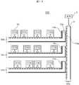
- FIG. 14shows a configuration example of the battery system 200 according to the fourth embodiment.
- the battery system 200includes a plurality of battery modules 220 (220-1 to 220-n) arranged three-dimensionally in a storage rack in the casing 210, and a transmitter / receiver corresponding to each of the battery modules.
- Communication terminal 230(230-1 to 230-n) incorporated, electromagnetic wave propagation device 100 connecting each communication terminal 230 and communication base station 7, and connected to communication base station 7 via control bus 242 And a battery system controller 240.
- the electromagnetic wave propagation device 100 shown in FIG. 6is disposed in a storage rack corresponding to the multipath environment in the housing 210, and control signals and data are transmitted between the communication terminal 230 and the battery system controller 240. Communication for transmitting and receiving such information is performed, and each battery module 220 is controlled by the battery system controller 240. It goes without saying that the electromagnetic wave propagation device 100 of other embodiments may be adopted.
- this electromagnetic wave propagation devicesince branch expansion of the propagation path can be performed with low loss while maintaining low leakage characteristics and high interference wave resistance, a plurality of batteries arranged three-dimensionally at various positions in the casing 210 Highly reliable communication is possible between the communication terminal 230 of the module 220 and the battery system controller 240.
- the electromagnetic wave propagation device 100By adopting the electromagnetic wave propagation device 100, there is no concern that the electromagnetic wave is irregularly reflected by the metal wall surface of the housing as in wireless communication, and the communication quality is unstable.
- the use of the electromagnetic wave propagation device 100eliminates the need for individual wiring, high breakdown voltage, free installation position, and easy maintenance can be achieved.
- the conventional detachable connectoris not required to connect multiple planar propagation media to electronic devices, so there is no need to expose electrodes and physically fix them, improving reliability, and reducing assembly and maintenance costs. Can be achieved. Furthermore, a high breakdown voltage can be achieved. Moreover, it is also possible to send the electric power which operates a battery module to the communication base station 7 and the communication terminal 230 by adding the function of a power transmission apparatus and a power receiving apparatus.
- the electromagnetic wave propagation device 100 of the present inventionis a system that includes a large number of electronic devices arranged three-dimensionally in a closed space inside a housing or indoors, and requires highly reliable communication with a center controller. It can also be applied to data centers, hard disk controllers, hospital medical diagnosis systems, traffic management centers, and the like.
- 1a, 1bplanar conductor
- 2a, 2bplanar dielectric
- 3a, 3bplanar dielectric spacer
- 4a, 4bplanar mesh conductor
- 5a, 5bslot
- 6parallel conversion interface
- 7Communication base station
- 8vertical conversion interface
- 9transceiver
- 10communication terminal
- 11a, 11bplanar conductor
- 12slot
- 13a, 13bsparse mesh conductor
- 14b-14dshield conductor
- 50a ⁇ 53a, 50b ⁇ 53bplanar propagation medium
- 100electromagnetic wave propagation device
- 200battery system.
Landscapes
- Near-Field Transmission Systems (AREA)
- Waveguide Aerials (AREA)
Abstract
Description
本発明は、電磁波伝搬路および電磁波伝搬装置に係り、特に、電磁波を伝搬させる面状伝搬媒体を用いた、3次元的な分岐拡張に適した電磁波伝搬路および電磁波伝搬装置に関するものである。The present invention relates to an electromagnetic wave propagation path and an electromagnetic wave propagation apparatus, and more particularly to an electromagnetic wave propagation path and an electromagnetic wave propagation apparatus suitable for three-dimensional branch expansion using a planar propagation medium for propagating electromagnetic waves.
近年、コンシューマ、社会インフラのあらゆる分野で電子機器のネットワーク化が進み、電子機器間を接続する配線コードの数が大幅に増加する傾向にある。同様に、電子機器の筐体内においても電子機器を構成するモジュール、電子部品間の配線数も増加の一途にあり、電子機器の小型化、低コスト化、信頼性向上を妨げている。In recent years, networking of electronic devices has progressed in every field of consumer and social infrastructure, and the number of wiring cords connecting electronic devices tends to increase significantly. Similarly, the number of wires between modules and electronic components constituting the electronic device is also increasing in the housing of the electronic device, which hinders downsizing, cost reduction, and reliability improvement of the electronic device.
無線LAN等の一般的な無線通信システムの導入が一つの配線削減手段であるが、無線通信システムでは筐体の金属壁面で電磁波が乱反射され、通信品質を不安定化させるという懸念点がある。
また、電子機器同士を結線するための従来の着脱式コネクタは、信頼性、コスト面での課題があり、物理的な着脱が不要で電極非露出の部品間接続へのニーズが増大している。The introduction of a general wireless communication system such as a wireless LAN is one of the wiring reduction means. However, in the wireless communication system, there is a concern that electromagnetic waves are irregularly reflected on the metal wall surface of the casing, thereby destabilizing communication quality.
In addition, conventional detachable connectors for connecting electronic devices have problems in reliability and cost, and there is an increasing need for connection between parts that do not require physical detachment and are not exposed to electrodes. .
これらの課題を解決する技術として、例えば、特許文献1には、2枚の面状導体で面状誘電体を挟み、その間で電磁波を伝達可能にするとともに、面状導体の一方をメッシュ状にして、薄膜の誘電体を介して電磁波伝搬装置のインターフェースを配置することで、メッシュ状導体近傍に滲み出るエバネッセント波により電磁波の出入を可能とする面状伝搬媒体が開示されている。同文献に記載されている技術では、電極となるメッシュ状導体とインターフェースの間に薄膜の誘電体が介在するため、物理的な着脱が不要であり、電極非露出の部品間接続が可能である。また、表面波と呼ばれる誘電体内を伝搬する電磁波を面状伝搬媒体内に閉じ込め、面状伝搬媒体に沿って2次元的に電力を伝送させるため、面状伝搬媒体外部への電磁波漏洩が小さく、金属筐体内の閉空間に設置しても乱反射による通信品質不安定化の問題が少ない。また、他システムによる外部からの妨害波に対する耐性が高いという特長も有する。また、特許文献1では、一つの面状伝搬媒体を2次元的な広がり方向に拡張するための技術が開示されている。すなわち、特許文献1では、二つの面状伝搬媒体の端面同士を対向させ、両者の接続部を表裏から挟むように覆う一対の導体板を備えることにより、面状伝搬媒体を低損失に拡張することが開示されている。As a technique for solving these problems, for example, inPatent Document 1, a planar dielectric is sandwiched between two planar conductors, and electromagnetic waves can be transmitted between them, and one of the planar conductors is meshed. Thus, a planar propagation medium is disclosed in which an electromagnetic wave propagating device interface is arranged through a thin film dielectric, thereby allowing electromagnetic waves to enter and exit by an evanescent wave that oozes out in the vicinity of the mesh conductor. In the technology described in this document, since a thin film dielectric is interposed between the mesh-like conductor serving as an electrode and the interface, physical attachment / detachment is unnecessary, and connection between parts without electrode exposure is possible. . In addition, electromagnetic waves propagating in a dielectric called surface waves are confined in a planar propagation medium, and power is transmitted two-dimensionally along the planar propagation medium, so that electromagnetic leakage outside the planar propagation medium is small, Even when installed in a closed space inside a metal casing, there are few problems of unstable communication quality due to diffuse reflection. Moreover, it has the feature that the tolerance with respect to the disturbance wave from the outside by other systems is high.Patent Document 1 discloses a technique for expanding one planar propagation medium in a two-dimensional spreading direction. That is, inPatent Document 1, the planar propagation medium is extended to low loss by providing a pair of conductor plates that face the end faces of the two planar propagation media and cover the connection portions of the two planar propagation media from both sides. It is disclosed.
また、特許文献2には、高周波線路の分岐拡張に関する技術が開示されている。すなわち、特許文献2には、誘電体層と、誘電体層を上下方向から挟み、誘電体層表面を被覆する、導電性材料から成る一対のグランド層とを積層し、同じく導電性材料から成る誘電体層内に配設された信号線で構成されたストリップ線路に関する技術であって、グランド層に開口部を設けた二つのストリップ線路同士を貼りあわせることで、電磁波を分岐させることが開示されている。Patent Document 2 discloses a technique related to branch expansion of a high-frequency line. That is, in Patent Document 2, a dielectric layer and a pair of ground layers made of a conductive material sandwiching the dielectric layer from above and below and covering the surface of the dielectric layer are laminated, and also made of a conductive material. Disclosed is a technology related to a strip line composed of signal lines arranged in a dielectric layer, in which electromagnetic waves are branched by bonding two strip lines each having an opening in a ground layer. ing.
特許文献1に記載の面状伝搬媒体の拡張技術は、一対の導体板を利用した2次元方向への媒体サイズ拡張に言及したものであり、筐体内に3次元配置された多数の電子機器や電子部品に電磁波を行き届かせるための3次元的な分岐拡張には適用困難である。特許文献1には、面状伝搬媒体が同一平面状で接続されるものに限定されず、その接続端部で折れ曲がるように任意の傾きを有するように接続しても良いとする例も記載されている。この例は、屋内の内壁面のような連続した面への適用は可能であるが、分岐拡張についての言及が無く、複数の面が立体的に配置されたような3次元的配置には適用が困難と考えられる。The planar propagation medium expansion technique described inPatent Document 1 refers to medium size expansion in a two-dimensional direction using a pair of conductor plates, and includes a large number of electronic devices arranged three-dimensionally in a housing. It is difficult to apply to the three-dimensional branch expansion for transmitting electromagnetic waves to electronic parts.Patent Document 1 also describes an example in which planar propagation media are not limited to those connected in the same plane, and may be connected so as to have an arbitrary inclination so as to be bent at the connection end. ing. This example can be applied to a continuous surface such as an indoor inner wall, but there is no mention of branch expansion and is applicable to a three-dimensional arrangement in which multiple surfaces are arranged in three dimensions. Is considered difficult.
特許文献2に記載の高周波線路の分岐拡張技術は、ストリップ線路を前提とし、二つのストリップ線路の開口部に設けたグランド層は物理的に接しており、電子機器の通信機器等と接する電極が露出している。この電極の露出は、部品が設置された一つのストリップ線路を、部品交換等のメンテナンスのために電子機器外に取り出す際に磨耗しやすいことから好ましくない。また、特許文献2に記載のストリップ線路は、表裏二つのグランド層を設けており、各グランド層と信号線間の電磁波エネルギーが1/2ずつであるので、一つのグランド層に開口部を設けても1/2以上の電磁波エネルギーの伝送ができず、高効率伝送が困難である。The branch and extension technique for a high-frequency line described in Patent Document 2 is based on a strip line, and the ground layer provided in the openings of the two strip lines is in physical contact, and an electrode in contact with a communication device or the like of an electronic device is provided. Exposed. This exposure of the electrodes is not preferable because one strip line on which components are installed is easily worn out when taken out of the electronic equipment for maintenance such as component replacement. In addition, the strip line described in Patent Document 2 is provided with two ground layers on the front and back sides, and the electromagnetic wave energy between each ground layer and the signal line is ½, so an opening is provided in one ground layer. However, it is difficult to transmit electromagnetic energy of 1/2 or more and high efficiency transmission.
また、特許文献2には、上記高周波線路ストリップ線路を屋内無線LANシステムに適用した態様も開示されているが、このような無線LAN親機と複数の無線LAN子機との無線通信には、上記のとおり、屋内の筐体等の金属壁面で電磁波が乱反射され、通信品質を不安定化させるという課題がある。Patent Document 2 also discloses an aspect in which the high-frequency line strip line is applied to an indoor wireless LAN system. However, in wireless communication between such a wireless LAN base unit and a plurality of wireless LAN slave units, As described above, there is a problem in that electromagnetic waves are irregularly reflected on a metal wall surface such as an indoor housing and the communication quality is destabilized.
本発明は、上記のような課題を解決するためになされたものであり、面状伝搬媒体の3次元的な分岐拡張を、物理的な着脱が不要で電極非露出に、低損失、低漏洩に実施することのできる電磁波伝搬路及び電磁波伝搬装置の提供を目的とする。The present invention has been made in order to solve the above-described problems. The three-dimensional branch expansion of the planar propagation medium is not required to be physically attached and removed, and the electrode is not exposed, with low loss and low leakage. It is an object of the present invention to provide an electromagnetic wave propagation path and an electromagnetic wave propagation device that can be implemented in the same manner.
本発明の代表的なものの一例を示すと次の通りである。本発明の電磁波伝搬装置は、複数の面状伝搬媒体と、前記複数の面状伝搬媒体間を隔離するために配置された面状誘電体スペーサと、前記面状伝搬媒体と送受信機との間で電磁波の送受を行なう第1のインターフェースとを備え、前記各面状伝搬媒体は、各々、少なくとも一つの面状導体と少なくとも一つの面状誘電体とを重ね合わせて構成され、前記各面状伝搬媒体は、他の少なくとも一つの前記面状伝搬媒体と、重なり部分を有するよう配置され、前記重なり部分の前記面状導体に、該面状伝搬媒体間で電磁波を送受する電磁波結合手段が設けられていることを特徴とする。An example of a representative example of the present invention is as follows. An electromagnetic wave propagation device according to the present invention includes a plurality of planar propagation media, a planar dielectric spacer disposed to isolate the plurality of planar propagation media, and between the planar propagation medium and a transceiver. And each of the planar propagation media is configured by superposing at least one planar conductor and at least one planar dielectric, each planar The propagation medium is arranged so as to have an overlapping portion with at least one other planar propagation medium, and an electromagnetic wave coupling means for transmitting and receiving electromagnetic waves between the planar propagation media is provided on the planar conductor of the overlapping portion. It is characterized by being.
本発明の電磁波伝搬装置によれば、伝搬経路の分岐拡張が低漏洩特性、高妨害波耐性を維持しつつ低損失でできるので、筐体内の様々な位置に3次元的に配置された複数の通信端末と高信頼な通信が可能となる。According to the electromagnetic wave propagation device of the present invention, branch expansion of a propagation path can be performed with low loss while maintaining low leakage characteristics and high interference wave resistance, and therefore, a plurality of three-dimensionally arranged at various positions in the housing Highly reliable communication with a communication terminal is possible.
本発明の代表的な実施形態では、上記目的を達成するために、電磁波伝搬装置が、少なくとも一つの面状導体と、少なくとも一つの面状誘電体を重ね合わせて構成された複数の面状伝搬媒体と、電子機器間で情報を送受する複数の送受信機と、前記送受信機と前記面状伝搬媒体の間で電磁波の送受を行なう第1のインターフェースとを備えている。この電磁波伝搬装置では、前記複数の面状伝搬媒体間にはそれぞれを隔離するための面状誘電体スペーサを設け、前記面状伝搬媒体は、他方の少なくとも一つの前記面状伝搬媒体と少なくとも一部が表裏に重なるように配置され、重なり部分の前記面状導体に前記面状伝搬媒体間で電磁波を送受する第2のインターフェースとして機能する電磁波結合手段を設けている。In an exemplary embodiment of the present invention, in order to achieve the above object, an electromagnetic wave propagation device includes a plurality of planar propagations configured by superposing at least one planar conductor and at least one planar dielectric. A medium; a plurality of transceivers for transmitting and receiving information between electronic devices; and a first interface for transmitting and receiving electromagnetic waves between the transceiver and the planar propagation medium. In this electromagnetic wave propagation device, a planar dielectric spacer for separating each of the plurality of planar propagation media is provided, and the planar propagation medium is at least one of the other at least one planar propagation medium. Electromagnetic wave coupling means functioning as a second interface for transmitting and receiving electromagnetic waves between the planar propagation media is provided on the planar conductors at the overlapping portions.
この電磁波伝搬装置によれば、低漏洩特性、高妨害波耐性を維持しつつ伝搬経路の分岐拡張が低損失でできるので、筐体内の様々な位置に配置された複数の通信端末と高信頼な通信が可能となる。また、複数の面状伝搬媒体の接続を電極非露出、物理的な固定不要の条件でできるため、組立てコスト、メンテナンスコストを削減できる。また、二つの面状伝搬媒体間および面状伝搬媒体とその上に配置される通信端末の間をそれぞれ直流近傍の低周波数帯において絶縁することができるので、例えば、面状伝搬媒体と通信端末間でグランド電位が異なり絶縁を要する用途に有用である。また、面状伝搬媒体は100ミクロン厚以下のフレキシブル性の高い基板を用いることができるので、筐体形状を問わず容易に実装できる。According to this electromagnetic wave propagation device, branch expansion of the propagation path can be performed with low loss while maintaining low leakage characteristics and high interference wave resistance, so that a plurality of communication terminals arranged at various positions in the housing can be highly reliable. Communication is possible. Further, since the connection of a plurality of planar propagation media can be performed under the condition that the electrode is not exposed and does not need to be physically fixed, the assembly cost and the maintenance cost can be reduced. In addition, since it is possible to insulate between the two planar propagation media and between the planar propagation medium and the communication terminal disposed thereon in a low frequency band near DC, for example, the planar propagation medium and the communication terminal This is useful for applications that require different ground potentials and require insulation. Further, since the planar propagation medium can use a highly flexible substrate having a thickness of 100 microns or less, it can be easily mounted regardless of the shape of the casing.
また、具体的な実施形態の電磁波伝搬装置では、前記面状伝搬媒体のうち少なくとも一つとして、面状導体、面状誘電体、面状メッシュ導体を順に重ねて構成し、前記面状メッシュ導体を前記第1のインターフェースとして用いている。
この実施形態の電磁波伝搬装置によれば、面状伝搬媒体上の通信端末の位置に依らず安定した通信を行なうことができる。In the electromagnetic wave propagation device of a specific embodiment, a planar conductor, a planar dielectric, and a planar mesh conductor are sequentially stacked as at least one of the planar propagation media, and the planar mesh conductor is formed. Is used as the first interface.
According to the electromagnetic wave propagation device of this embodiment, stable communication can be performed regardless of the position of the communication terminal on the planar propagation medium.
また、具体的な他の実施形態の電磁波伝搬装置では、前記面状伝搬媒体のうち少なくとも一つとして、第1の面状導体、面状誘電体、第2の面状導体を順に重ねて構成し、前記第2の面状導体に設けたスロットを前記第1のインターフェースとして用いている。
この実施形態の電磁波伝搬装置によれば、予め定められた通信端末の位置以外からの電磁波漏洩を低減し、面状伝搬媒体内の伝搬効率を向上させることができる。In addition, in the electromagnetic wave propagation device according to another specific embodiment, the first planar conductor, the planar dielectric, and the second planar conductor are sequentially stacked as at least one of the planar propagation media. A slot provided in the second planar conductor is used as the first interface.
According to the electromagnetic wave propagation device of this embodiment, leakage of electromagnetic waves from other than the predetermined position of the communication terminal can be reduced, and propagation efficiency in the planar propagation medium can be improved.
また、具体的な他の実施形態の電磁波伝搬装置では、前記電磁波結合手段の少なくとも一つとして、前記少なくとも二つの面状伝搬媒体の重なり部分の前記面状導体にスロット(開口部)を設けている。
この実施形態の電磁波伝搬装置によれば、面状伝搬媒体間の伝搬効率を向上させることができ、前記スロットの寸法により伝搬効率を可変とすることができる。In addition, in an electromagnetic wave propagation device according to another specific embodiment, as at least one of the electromagnetic wave coupling means, a slot (opening) is provided in the planar conductor in an overlapping portion of the at least two planar propagation media. Yes.
According to the electromagnetic wave propagation device of this embodiment, the propagation efficiency between the planar propagation media can be improved, and the propagation efficiency can be made variable according to the size of the slot.
また、具体的な他の実施形態の電磁波伝搬装置では、前記電磁波結合手段の少なくとも一つとして、前記少なくとも二つの面状伝搬媒体の重なり部分の前記面状導体にメッシュ構造を設けている。
この実施形態の電磁波伝搬装置によれば、面状伝搬媒体の広がり方向の位置ズレによる面状伝搬媒体間の伝搬効率の変動を小さく出来る。In an electromagnetic wave propagation device according to another specific embodiment, as at least one of the electromagnetic wave coupling means, a mesh structure is provided on the planar conductor in an overlapping portion of the at least two planar propagation media.
According to the electromagnetic wave propagation device of this embodiment, it is possible to reduce the fluctuation in propagation efficiency between the planar propagation media due to the positional deviation in the spreading direction of the planar propagation medium.
また、具体的な他の実施形態の電磁波伝搬装置では、前記複数の面状伝搬媒体が、1つの第1の面状伝搬媒体と複数の第2の面状伝搬媒体とで構成され、前記第2の面状伝搬媒体は、前記第1の面状伝搬媒体内の電磁波の伝搬方向に対し、少なくとも一部が表裏に重なるように構成された前記重なり部分と、前記第2の面状伝搬媒体の電磁波の伝搬方向を傾けるように、前記重なり部分に対して曲げて構成された他の部分とを有する。
この実施形態の電磁波伝搬装置によれば、様々な方向への分岐拡張が低漏洩特性、高妨害波耐性を維持したまま実施できる。
以下、本発明の実施形態について、図面を参照しながら、詳細に説明する。In the electromagnetic wave propagation device according to another specific embodiment, the plurality of planar propagation media includes a first planar propagation medium and a plurality of second planar propagation media. The planar transmission medium 2 includes the overlapping portion configured to overlap at least partly with respect to the propagation direction of the electromagnetic wave in the first planar propagation medium, and the second planar propagation medium. And the other part bent to the overlapping part so as to incline the propagation direction of the electromagnetic wave.
According to the electromagnetic wave propagation device of this embodiment, branch expansion in various directions can be performed while maintaining low leakage characteristics and high interference wave resistance.
Hereinafter, embodiments of the present invention will be described in detail with reference to the drawings.
本発明の実施形態1について、図1A~図3を参照しながら説明する。
図1Aは、実施形態1に係る電磁波伝搬装置における、電磁波伝搬路を構成する二つの面状伝搬媒体の電磁波結合手段の例を示している。また、図1Bは、電磁波伝搬装置の構成図であり、分かり易くするために、主要な面が表示されるように分解した斜視図である。Embodiment 1 of the present invention will be described with reference to FIGS. 1A to 3.
FIG. 1A shows an example of electromagnetic wave coupling means of two planar propagation media constituting an electromagnetic wave propagation path in the electromagnetic wave propagation device according to the first embodiment. FIG. 1B is a configuration diagram of the electromagnetic wave propagation device, and is an exploded perspective view in which main surfaces are displayed for easy understanding.
図1Aは、実施形態1に係る電磁波伝搬装置における、電磁波伝搬路を構成する二つの面状伝搬媒体の電磁波結合手段の例を示している。また、図1Bは、電磁波伝搬装置の構成図であり、分かり易くするために、主要な面が表示されるように分解した斜視図である。
FIG. 1A shows an example of electromagnetic wave coupling means of two planar propagation media constituting an electromagnetic wave propagation path in the electromagnetic wave propagation device according to the first embodiment. FIG. 1B is a configuration diagram of the electromagnetic wave propagation device, and is an exploded perspective view in which main surfaces are displayed for easy understanding.
電磁波伝搬装置100は、少なくとも1つの通信基地局7と複数の通信端末10(10-1~10-n)間で情報を送受信する装置であり、面状伝搬媒体50a、50b、及び、平行変換型インターフェース6を備える。各通信端末10は、例えば、複数の電子機器の各々に通信モジュールとして組み込まれ、通信基地局7と通信を行う送受信機である。通信に使用される電磁波の周波数は、例えば、2.5GHzや900MHzである。通信端末10は、垂直変換型インターフェース8と送受信機9を備え、平行変換型インターフェース(第3のインターフェース)6と面状伝搬媒体50a、50bを介して、通信基地局7と通信信号を送受する。
二つの面状伝搬媒体50a、50bは、それらの一部分、例えば端部近傍で、表裏が重なるようにして重ねて配置され、この重なり部分に電磁波結合手段が設けられ、通信信号としての電磁波の伝搬経路を成す。第1、第2の面状伝搬媒体50a、50bは、それぞれ、面状導体1a、1b、面状誘電体2a、2b、面状メッシュ導体4a、4b、面状誘電体スペーサ3a、3bの各部材を順に重ねて構成される。The electromagneticwave propagation device 100 is a device that transmits and receives information between at least onecommunication base station 7 and a plurality of communication terminals 10 (10-1 to 10-n), and includesplanar propagation media mold interface 6 is provided. Eachcommunication terminal 10 is, for example, a transceiver that is incorporated as a communication module in each of a plurality of electronic devices and communicates with thecommunication base station 7. The frequency of the electromagnetic wave used for communication is, for example, 2.5 GHz or 900 MHz. Thecommunication terminal 10 includes avertical conversion interface 8 and a transceiver 9, and transmits and receives communication signals to and from thecommunication base station 7 via the parallel conversion interface (third interface) 6 and theplanar propagation media
The twoplanar propagation media planar propagation media planar conductors planar dielectrics planar mesh conductors dielectric spacers
二つの面状伝搬媒体50a、50bは、それらの一部分、例えば端部近傍で、表裏が重なるようにして重ねて配置され、この重なり部分に電磁波結合手段が設けられ、通信信号としての電磁波の伝搬経路を成す。第1、第2の面状伝搬媒体50a、50bは、それぞれ、面状導体1a、1b、面状誘電体2a、2b、面状メッシュ導体4a、4b、面状誘電体スペーサ3a、3bの各部材を順に重ねて構成される。The electromagnetic
The two
面状メッシュ導体4a、4bは碁盤目状になって広がっており、メッシュのピッチによって、電磁波が外界へ滲み出す量を制御することができる。エバネッセント波と呼ばれる外界へ滲み出す電磁波は、伝搬距離に対して指数関数的に減衰する。典型的には、振幅が1/eに減衰する距離は1cm程度である(e:自然対数の底)。従って、面状メッシュ導体4b近傍にのみ電磁波を局在させ、外界への不要放射を極めて小さくできる。また、放射素子の可逆原理により、外界からの妨害波からの影響をほとんど受けない。面状メッシュ導体4bは通信端末10とのインターフェース(第1のインターフェース)として機能する。Theplanar mesh conductors planar mesh conductor 4b, and unnecessary radiation to the outside can be made extremely small. Further, due to the reversible principle of the radiating element, it is hardly affected by interference waves from the outside. Theplanar mesh conductor 4b functions as an interface (first interface) with thecommunication terminal 10.
面状誘電体2a、2bは、伝搬効率を考慮すると低誘電率かつ低誘電正接である材料が望ましい。面状誘電体スペーサ3a、3bは面状メッシュ導体4a、4bを保護するのと同時に、面状誘電体スペーサ3aは二つの面状伝搬媒体50a、50b間を、面状誘電体スペーサ3bは面状伝搬媒体50bとその上に配置される通信端末10の間を、それぞれ直流近傍の低周波数帯において絶縁する役割を持つ。Theplanar dielectrics dielectric spacers planar mesh conductors dielectric spacer 3a is between the twoplanar propagation media dielectric spacer 3b is a surface. It has a role to insulate between thestate propagation medium 50b and thecommunication terminal 10 disposed thereon in a low frequency band near DC.
ここで、二つの面状伝搬媒体50a、50bの重なり部分の距離をLとする。本実施形態では、L=Lmc1、第1の面状伝搬媒体50aの端面からスロット5bまでの距離をLmt1、第2の面状伝搬媒体50bの端面からスロット5bまでの距離をLmt2とする。この重なり部分Lに設けられたスロット5bが、第1、第2の面状伝搬媒体50a、50b間で電磁波を送受するインターフェース(第2のインターフェース)の役割を果たす。すなわち、スロット5bは電磁波結合手段として機能する。Here, let L be the distance between the overlapping portions of the twoplanar propagation media planar propagation medium 50a to theslot 5b is Lmt1, and the distance from the end face of the secondplanar propagation medium 50b to theslot 5b is Lmt2. Theslot 5b provided in the overlapping portion L serves as an interface (second interface) for transmitting and receiving electromagnetic waves between the first and secondplanar propagation media slot 5b functions as electromagnetic wave coupling means.
なお、図1Bでは、分かり易くするために、スロット5bを面状誘電体スペーサ3a上に表示しているが、このスロット5bは第2の面状伝搬媒体50bの下面に形成されていても良く、あるいはスロット5bを含む電磁波伝搬装置100の各層をさらに細かく分解して形成しても良い。このように、図1A、図1Bに示した電磁波伝搬装置100は、全体として上記構成を具備していれば良く、それらの構成要素の区分は任意であり、また、この区分に沿って製造方法を適宜選択すればよい(以下の実施例でも同様)。In FIG. 1B, for the sake of clarity, theslot 5b is displayed on the planardielectric spacer 3a. However, theslot 5b may be formed on the lower surface of the secondplanar propagation medium 50b. Alternatively, each layer of the electromagneticwave propagation device 100 including theslot 5b may be further finely disassembled. Thus, the electromagneticwave propagation device 100 shown in FIGS. 1A and 1B only needs to have the above-described configuration as a whole, and the division of these components is arbitrary, and the manufacturing method along this division May be appropriately selected (the same applies to the following examples).
平行変換型インターフェース6は、通信基地局7と面状伝搬媒体50aを接続するインターフェースであり、両者は電磁波の進行方向に対して平行に配置され、通信基地局7から出力された同軸線路モード等の電磁波を、面状伝搬媒体50aの表面波モードにモード変換する。通信基地局7は、平行変換型インターフェース6および面状伝搬媒体50a、50bを介して通信端末10と通信信号を送受する装置である。通信端末10の垂直変換型インターフェース8は、面状伝搬媒体50bから通信信号を受け取るためのインターフェースであり、この垂直変換型インターフェース8は面状伝搬媒体50bにおける電磁波の進行方向に対して垂直に配置され、面状伝搬媒体50bの表面波モードを同軸線路モード等の電磁波にモード変換する。このように、電磁波は、表面波モードから、エバネッセント波に変換され、さらに同軸線路モードに変換される。Theparallel conversion interface 6 is an interface for connecting thecommunication base station 7 and theplanar propagation medium 50a, both of which are arranged in parallel to the traveling direction of the electromagnetic wave, and the coaxial line mode output from thecommunication base station 7 or the like. Is converted into the surface wave mode of theplanar propagation medium 50a. Thecommunication base station 7 is a device that transmits and receives communication signals to and from thecommunication terminal 10 via theparallel conversion interface 6 and theplanar propagation media vertical conversion interface 8 of thecommunication terminal 10 is an interface for receiving a communication signal from theplanar propagation medium 50b, and thevertical conversion interface 8 is arranged perpendicular to the traveling direction of the electromagnetic wave in theplanar propagation medium 50b. Then, the surface wave mode of theplanar propagation medium 50b is mode-converted into an electromagnetic wave such as a coaxial line mode. As described above, the electromagnetic wave is converted from the surface wave mode to the evanescent wave, and further converted to the coaxial line mode.
面状伝搬媒体50a、50bは、各々、2次元的な広がりを持たせて表面波と呼ばれる電磁波を広域に伝搬させることができるが、ここでは典型例として、平行変換型インターフェース6から面状伝搬媒体50aの長手方向に沿って表面波が伝搬すると仮定して説明する。また、本構成では面状伝搬媒体50a、50bの短手方向に存在する二つの端面は開放構造となっているため、寸法の制限無く全周波数帯の電磁波伝搬が可能である。しかし、二つの端面が短絡構造となっている場合は、面状伝搬媒体50a、50bの短手方向の長さが1/2λg以上(λg:実効波長)となるように寸法を選ぶ必要がある。さらに、面状伝搬媒体50bの端面が短絡もしくは開放の反射端の場合、内部で定在波が励起され、その上に配置される通信端末10の位置によって受けられる電磁波エネルギーにバラツキが生じ、通信品質に偏差が現れる可能性がある。本現象の対策としては面状伝搬媒体50bの端面に、使用周波数帯で動作する電波吸収体を配置することが有効である。Each of theplanar propagation media planar propagation medium parallel conversion interface 6 here. The description will be made on the assumption that a surface wave propagates along the longitudinal direction of the medium 50a. Further, in this configuration, the two end surfaces existing in the short direction of theplanar propagation media planar propagation media planar propagation medium 50b is a short-circuited or open reflection end, a standing wave is excited inside, and the electromagnetic energy received by the position of thecommunication terminal 10 disposed thereon varies, thereby causing communication. There may be deviations in quality. As a countermeasure against this phenomenon, it is effective to arrange a radio wave absorber that operates in the used frequency band on the end face of theplanar propagation medium 50b.
先に述べたように、面状導体1bの端部近傍の重なり部分に空けられているスロット5bは、二つの面状伝搬媒体50a、50b間で電磁波を送受するインターフェース(第2のインターフェース)の役割を果たす。スロット5bは面状メッシュ導体4a、4bに電磁シールドされているので、外界への不要放射を極めて小さくできる。また同様に、外界からの妨害波からの影響をほとんど受けない。ここで、スロット5bの寸法を、面状伝搬媒体50aの長手方向の長さをSmw1、短手方向の長さをSme1と定義する。スロット5bは使用周波数λgにおいて共振を励起させることが面状伝搬媒体間の伝搬効率が良く、短手方向の長さSme1≒(2n-1)・λg/2に設定することが望ましい。ここでnは自然数である。一方、長手方向の長さSmw1はプリント基板の一般的な最小加工寸法である0.1mm以上あれば問題ない。もちろん、複数の面状伝搬媒体を用いるようなケースでは、上述のような寸法を増減させてスロット毎に伝搬効率の調整を行なうことが可能である。調整の手段として、スロット自身の位置を面状伝搬媒体50aの長辺側に位置オフセットさせても良い。また、面状伝搬媒体50aに伝搬させる電磁波の周波数によって様々な伝搬モードが成立するため、Smw1とSme1の寸法を入れ替え、面状伝搬媒体50aの長辺側に位置オフセットさせる、スロットの重心を軸に45度回転させる、スロットを十字型にする等の方策も有効である。As described above, theslot 5b opened in the overlapping portion in the vicinity of the end of theplanar conductor 1b is an interface (second interface) for transmitting and receiving electromagnetic waves between the twoplanar propagation media slot 5b is electromagnetically shielded by theplanar mesh conductors slot 5b is defined as Smw1 in the longitudinal direction of theplanar propagation medium 50a and Sme1 in the short direction. Theslot 5b is preferably set to a length Sme1≈ (2n−1) · λg / 2 in the short direction by exciting the resonance at the use frequency λg to improve the propagation efficiency between the planar propagation media. Here, n is a natural number. On the other hand, there is no problem if the length Smw1 in the longitudinal direction is 0.1 mm or more, which is a general minimum processing dimension of the printed circuit board. Of course, in the case of using a plurality of planar propagation media, it is possible to adjust the propagation efficiency for each slot by increasing or decreasing the dimensions as described above. As an adjustment means, the position of the slot itself may be offset to the long side of theplanar propagation medium 50a. Further, since various propagation modes are established depending on the frequency of the electromagnetic wave propagating to theplanar propagation medium 50a, the dimensions of Smw1 and Sme1 are switched, and the center of gravity of the slot is offset to the long side of theplanar propagation medium 50a. Measures such as 45 degrees rotation and a cross-shaped slot are also effective.
なお、本発明における二つの面状伝搬媒体の部分的な重なりは、端部近傍に限定されるものではない。例えば、下側に位置する第1の面状伝搬媒体50aの面積が上側に位置する第2の面状伝搬媒体50bよりも大きく、第1の面状伝搬媒体50aの端部よりも内側において、表裏が部分的に重なるようにして重ねて配置されるものでも良い。It should be noted that the partial overlap of the two planar propagation media in the present invention is not limited to the vicinity of the end. For example, the area of the firstplanar propagation medium 50a located on the lower side is larger than that of the secondplanar propagation medium 50b located on the upper side, and inside the end of the firstplanar propagation medium 50a, It may be arranged so that the front and back are partially overlapped.
図2は、二つの面状伝搬媒体50a、50bの一部を重ねて配置し拡張した電磁波伝搬装置100の断面図である。面状伝搬媒体50aは、面状伝搬媒体50bとの重なり部分(L=Lmc1)と重ならない部分とで特性インピーダンスが異なる為、その境界で表面波の反射が起こり、全体の伝搬効率の低下や定在波励起による通信品質の位置バラツキ等の問題を引き起こす。反射を最小とするには、Lmc1≒(2n-1)・λg/4に設定することが望ましい。FIG. 2 is a cross-sectional view of the electromagneticwave propagation device 100 in which twoplanar propagation media planar propagation medium 50a has different characteristic impedances in the overlapping part (L = Lmc1) with theplanar propagation medium 50b and the non-overlapping part. Therefore, reflection of surface waves occurs at the boundary, and the overall propagation efficiency decreases. It causes problems such as position variations in communication quality due to standing wave excitation. In order to minimize reflection, it is desirable to set Lmc1≈ (2n−1) · λg / 4.
また、スロット5bの伝搬効率を向上させるには、スロット5bの位置で電界が最大となるようにLmt1、Lmt2を決めればよく、面状伝搬媒体50a、50bの端面が開放端の場合(図2(b))は、Lmt1=Lmt2≒n・λg/2、金属による短絡端の場合(図2(a))は、Lmt1=Lmt2≒(2n-1)・λg/4となるように設定することが望ましい。In order to improve the propagation efficiency of theslot 5b, Lmt1 and Lmt2 may be determined so that the electric field is maximized at the position of theslot 5b. When the end surfaces of theplanar propagation media
以上は、面状伝搬媒体50a、50bに用いる材料、厚み等が同一であると仮定した場合であり、異なる場合はLmt1、Lmt2を個別に設定する必要がある。The above is a case where the materials, thicknesses, and the like used for theplanar propagation media
図3は、3次元的な分岐拡張を実現するために、1つの直線状の面状伝搬媒体(第1の面状伝搬媒体)50aと複数のL字型の面状伝搬媒体(第2の面状伝搬媒体)50b~50dとが、各第2の面状伝搬媒体の端部近傍でその一部分を第1の面状伝搬媒体の表面に重ねて配置された電磁波伝搬装置100の断面図である。複数の第2の面状伝搬媒体50b~50dが、第1の面状伝搬媒体50aにその軸方向に間隔をおいて接続されている。第1の面状伝搬媒体50aから第2の面状伝搬媒体50b~50dへの電磁波はそれぞれ、第1の面状伝搬媒体50aと同じ伝搬方向で長さLnc1の重なり部分に設けられた電磁波結合手段であるスロット5b~5dを介して入力される。FIG. 3 shows one linear planar propagation medium (first planar propagation medium) 50a and a plurality of L-shaped planar propagation media (second (Planar propagation media) 50b to 50d are cross-sectional views of the electromagneticwave propagation device 100 in which a portion of each of the second planar propagation media is disposed in the vicinity of the end of each second planar propagation medium so as to overlap the surface of the first planar propagation medium. is there. A plurality of secondplanar propagation media 50b to 50d are connected to the firstplanar propagation medium 50a at intervals in the axial direction thereof. The electromagnetic waves from the firstplanar propagation medium 50a to the secondplanar propagation media 50b to 50d are electromagnetic wave couplings provided at overlapping portions of the length Lnc1 in the same propagation direction as the firstplanar propagation medium 50a. It is input viaslots 5b to 5d as means.
複数の第2の面状伝搬媒体50b~50dが、第1の面状伝搬媒体50aに対して垂直となるようにL字型に曲げている目的は、面状伝搬媒体50a内の表面波の伝搬方向に対して垂直方向へも伝搬させ、さらに、分岐経路への電磁波の分配比率を可変とするよう重なり部分の長さを調節するためである。なお、本図では簡単のため面状伝搬媒体50b~50dを直角に曲げているが、緩やかなRをつけて曲げる方が伝搬損失や反射損失が少なくできることは言うまでもない。The purpose of the plurality of secondplanar propagation media 50b to 50d being bent in an L shape so as to be perpendicular to the firstplanar propagation medium 50a is that of the surface wave in theplanar propagation medium 50a. This is because the length of the overlapping portion is adjusted so as to propagate in the direction perpendicular to the propagation direction and further to change the distribution ratio of the electromagnetic wave to the branch path. In this figure, theplanar propagation media 50b to 50d are bent at right angles for the sake of simplicity, but it goes without saying that bending loss with a gentle R can reduce propagation loss and reflection loss.
第1の面状伝搬媒体50aから第2の面状伝搬媒体50b~50dへの分配比率が同程度となるようにするには、前述したようなスロット寸法の調整が必要である。典型的には、第2の面状伝搬媒体(50b、50c、50d)が平行変換型インターフェース6から離れるに従って、対応するスロット(5b、5c、5d)の寸法(図1BのSmw1、Sme1相当)を順次大きくすることで、同程度の分配比率とすることが可能である。To adjust the distribution ratio from the firstplanar propagation medium 50a to the secondplanar propagation media 50b to 50d to the same level, it is necessary to adjust the slot dimensions as described above. Typically, as the second planar propagation medium (50b, 50c, 50d) moves away from theparallel conversion interface 6, the dimensions of the corresponding slots (5b, 5c, 5d) (corresponding to Smw1, Sme1 in FIG. 1B) By sequentially increasing, it is possible to achieve the same distribution ratio.
また、重なり部分の寸法Lについては、面状伝搬媒体50a、50bの重なり部分を代表例として説明する。重なり部分の距離をLnc1、面状伝搬媒体50bの端面からスロット5bまでの距離をLnt1とし、面状伝搬媒体50a、50bに用いる材料、厚み等が同一であると仮定する。前述したように面状伝搬媒体50aは面状伝搬媒体50bとの重なり部分と重ならない部分で特性インピーダンスが異なる為、その境界で表面波の反射が起こり、全体の伝搬効率の低下や定在波励起による通信品質の位置バラツキ等の問題を引き起こす。反射を最小とするには、Lnc1≒(2n-1)・λg/4に設定することが望ましい。また、スロット5bの伝搬効率を向上させるには、スロット5bの位置で電界が最大となるようにLnt1を決めればよく、面状伝搬媒体50bの端面が開放端の場合はLnt1≒n・λg/2、短絡端の場合はLnt1≒(2n-1)・λg/4となるように設定することが望ましい。以上は、スロット5c、5dについても同様に当てはまるが、Lnc1、Lnt1を、分配比率を変えるためのパラメータとすることもできる。The overlapping portion dimension L will be described using the overlapping portion of theplanar propagation media planar propagation medium 50b to theslot 5b is Lnt1, and the materials, thicknesses, and the like used for theplanar propagation media planar propagation medium 50a has a different characteristic impedance in a portion that does not overlap with the overlapping portion with theplanar propagation medium 50b. Therefore, reflection of surface waves occurs at the boundary, resulting in a decrease in the overall propagation efficiency and standing waves. This causes problems such as position variations in communication quality due to excitation. In order to minimize reflection, it is desirable to set Lnc1≈ (2n−1) · λg / 4. In order to improve the propagation efficiency of theslot 5b, Lnt1 may be determined so that the electric field is maximized at the position of theslot 5b. When the end surface of theplanar propagation medium 50b is an open end, Lnt1≈n · λg / 2. In the case of a short-circuited end, it is desirable to set so that Lnt1≈ (2n−1) · λg / 4. The above applies to theslots
本実施形態は、2個または4個の面状伝搬媒体を用いた伝搬経路の分岐拡張について説明したが、それ以上の面状伝搬媒体についても同様に実施することができる。また、二つの面状伝搬媒体の接続に一つのスロットを用いたが、二つ以上のスロットを設けてより両者間の伝搬効率を上げることも可能である。In the present embodiment, the branch extension of the propagation path using two or four planar propagation media has been described. However, the present invention can be similarly applied to other planar propagation media. In addition, although one slot is used to connect two planar propagation media, it is possible to increase the propagation efficiency between the two by providing two or more slots.
また、本実施形態は通信端末の下面と面状伝搬媒体が接する構成として説明したが、天地を逆転させて、通信端末の上面と面状伝搬媒体が接する構成にしてもよい。In addition, although the present embodiment has been described as a configuration in which the lower surface of the communication terminal is in contact with the planar propagation medium, a configuration in which the upper surface of the communication terminal is in contact with the planar propagation medium may be reversed.
以上のように、本実施形態1に係る電磁波伝搬装置100は、複数の面状伝搬媒体を、スロット(第2のインターフェース)を介して接続することにより、低漏洩特性、高妨害波耐性を維持しつつ伝搬経路の分岐拡張、特に3次元的な分岐拡張、が低損失でできるので、筐体内の様々な位置に3次元的に配置された複数の通信端末と、電磁波伝搬路を介して高信頼な通信が可能となる。As described above, the electromagneticwave propagation device 100 according to the first exemplary embodiment maintains a low leakage characteristic and a high interference wave resistance by connecting a plurality of planar propagation media via a slot (second interface). However, since branch expansion of the propagation path, particularly three-dimensional branch expansion, can be performed with low loss, a plurality of communication terminals that are three-dimensionally arranged at various positions in the housing and high frequency via the electromagnetic wave propagation path. Reliable communication is possible.
また、本実施形態1によれば、複数の面状伝搬媒体の接続を電極非露出、物理的な固定不要でできるため、組立てコスト、メンテナンスコストを削減できる。In addition, according to the first embodiment, the connection of a plurality of planar propagation media can be made without exposing the electrodes and requiring no physical fixation, so that the assembly cost and the maintenance cost can be reduced.
また、本実施形態1によれば、面状メッシュ導体は周期構造であるため、スロット寸法であるSme1の値を面状伝搬媒体の短手方向の長さよりも十分小さく設定することで、面状伝搬媒体の広がり方向の位置ズレによる面状伝搬媒体間の伝搬効率の変動を小さく出来る。Further, according to the first embodiment, since the planar mesh conductor has a periodic structure, the value of the slot dimension Sme1 is set to be sufficiently smaller than the length of the planar propagation medium in the short direction, thereby forming the planar mesh conductor. Variations in propagation efficiency between planar propagation media due to misalignment in the spreading direction of the propagation media can be reduced.
また、本実施形態1によれば、面状誘電体スペーサにより二つの面状伝搬媒体間および面状伝搬媒体とその上に配置される通信端末の間をそれぞれ直流近傍の低周波数帯において絶縁することができるので、例えば、面状伝搬媒体と通信端末間でグランド電位が異なり絶縁を要する用途に有用である。Further, according to the first embodiment, the planar dielectric spacers insulate between the two planar propagation media and between the planar propagation medium and the communication terminal disposed thereon in a low frequency band near DC. Therefore, for example, the ground potential is different between the planar propagation medium and the communication terminal, which is useful for applications that require insulation.
また、本実施形態1によれば、面状伝搬媒体は100ミクロン厚以下のフレキシブル性の高い、例えばフィルム基板を用いることができるので、筐体が平面であっても曲面であっても実装することは容易である。Further, according to the first embodiment, the planar propagation medium can be a flexible film having a thickness of 100 microns or less, for example, a film substrate. Therefore, the planar propagation medium can be mounted regardless of whether the casing is flat or curved. It is easy.
また、本実施形態1は通信装置として説明したが、通信基地局7、送受信機9をそれぞれ送電装置、受電装置に置き換えることで、電磁波を通信信号として送るのではなく、電子機器を動作させる電力として送ることも可能である。もちろん、両者を同時もしくは時分割に送ることも組み合わせの構成で実現できることは言うまでもない。Moreover, although thisEmbodiment 1 demonstrated as a communication apparatus, by replacing thecommunication base station 7 and the transmitter / receiver 9 with a power transmission apparatus and a power receiving apparatus, respectively, the electric power which operates an electronic device instead of sending electromagnetic waves as a communication signal. It is also possible to send as. Of course, it is needless to say that both can be sent simultaneously or in a time-division manner with a combined configuration.
次に、本発明の実施形態2について、図4~図9を参照しながら説明する。
図4は、実施形態2に係る電磁波伝搬装置における、面状伝搬媒体の電磁波結合手段の断面図である。Next, a second embodiment of the present invention will be described with reference to FIGS.
FIG. 4 is a cross-sectional view of the electromagnetic wave coupling means of the planar propagation medium in the electromagnetic wave propagation device according to the second embodiment.
電磁波伝搬装置100は、通信基地局7と通信端末10で情報を送受信する装置であり、面状伝搬媒体51a、51b、平行変換型インターフェース6を備える。
二つの面状伝搬媒体50a、50bは、それらの端部近傍で表裏が重なるようにして重ねて配置され、この重なり部分に電磁波結合手段が設けられ、通信信号としての電磁波の伝搬経路を成す。ここで、重なり部分の距離をLとする。本実施形態では、面状伝搬媒体51aの端面からスロット5aまでの距離をLpt1、面状伝搬媒体51bの端面からスロット5bまでの距離をLpt2とする。従って、重なり部分の距離L=Lpt1+Lpt2となる。The electromagneticwave propagation device 100 is a device that transmits and receives information between thecommunication base station 7 and thecommunication terminal 10, and includesplanar propagation media parallel conversion interface 6.
The twoplanar propagation media planar propagation medium 51a to theslot 5a is Lpt1, and the distance from the end surface of theplanar propagation medium 51b to theslot 5b is Lpt2. Accordingly, the overlap distance L = Lpt1 + Lpt2.
二つの面状伝搬媒体50a、50bは、それらの端部近傍で表裏が重なるようにして重ねて配置され、この重なり部分に電磁波結合手段が設けられ、通信信号としての電磁波の伝搬経路を成す。ここで、重なり部分の距離をLとする。本実施形態では、面状伝搬媒体51aの端面からスロット5aまでの距離をLpt1、面状伝搬媒体51bの端面からスロット5bまでの距離をLpt2とする。従って、重なり部分の距離L=Lpt1+Lpt2となる。The electromagnetic
The two
スロット5a、5bの伝搬効率を向上させるには、スロット5a、5bの位置で電界が最大となるようにLpt1、Lpt2をそれぞれ決めればよく、面状伝搬媒体51a、51bの端面が開放端の場合はLpt1=Lpt2≒n・λg/2、短絡端の場合はLpt1=Lpt2≒(2n-1)・λg/4となるように設定することが望ましい。以上は、面状伝搬媒体51a、51bに用いる材料、厚み等が同一であると仮定した場合であり、異なる場合はLpt1、Lpt2は個別に設定する必要がある。In order to improve the propagation efficiency of theslots slots planar propagation media planar propagation media
図5は、実施形態2に係る電磁波伝搬装置の主要な面が表示されるように分解した斜視図である。
二つの面状伝搬媒体51a、51bは、それらの端部近傍で重なるようにして重ねて配置され、この重なり部分に電磁波結合手段が設けられ、通信信号としての電磁波の伝搬経路を成す。面状伝搬媒体51a、51bはそれぞれ、面状導体1a、1b、面状誘電体2a、2b、面状導体11a、11b、面状誘電体スペーサ3a、3bを順に重ねて構成される。FIG. 5 is an exploded perspective view so that main surfaces of the electromagnetic wave propagation device according to the second exemplary embodiment are displayed.
The twoplanar propagation media planar propagation media planar conductors planar dielectrics planar conductors dielectric spacers
二つの面状伝搬媒体51a、51bは、それらの端部近傍で重なるようにして重ねて配置され、この重なり部分に電磁波結合手段が設けられ、通信信号としての電磁波の伝搬経路を成す。面状伝搬媒体51a、51bはそれぞれ、面状導体1a、1b、面状誘電体2a、2b、面状導体11a、11b、面状誘電体スペーサ3a、3bを順に重ねて構成される。FIG. 5 is an exploded perspective view so that main surfaces of the electromagnetic wave propagation device according to the second exemplary embodiment are displayed.
The two
面状伝搬媒体51a、51bは2次元的な広がりを持たせて平行平板モードの電磁波を広域に伝搬させることができるが、ここでは典型例として、平行変換型インターフェース6から面状伝搬媒体51aの長手方向に沿って電磁波が伝搬すると仮定して説明する。また、本構成では面状伝搬媒体51a、51bの短手方向に存在する二つの端面は開放構造(平行平板モード)となっているため、寸法の制限無く全周波数帯の電磁波伝搬が可能である。しかし、二つの端面が短絡構造となっている場合は、導波管モードが伝搬できるよう面状伝搬媒体51a、51bの短手方向の長さが1/2λg以上となるように寸法を選ぶ必要がある。さらに、面状伝搬媒体51bの端面が短絡もしくは開放の反射端の場合、内部で定在波が励起され、その上に配置される通信端末10の位置によって受けられる電磁波エネルギーにバラツキが生じ、通信品質に偏差が現れる可能性がある。本現象の対策としては面状伝搬媒体51bの端面に、使用周波数帯で動作する電波吸収体を配置することが有効である。Theplanar propagation media planar propagation medium 51a has aplanar propagation medium 51a. The description will be made on the assumption that electromagnetic waves propagate along the longitudinal direction. Further, in this configuration, the two end faces existing in the lateral direction of theplanar propagation media planar propagation media planar propagation medium 51b is a short-circuited or open reflection end, a standing wave is excited inside, and the electromagnetic wave energy received by the position of thecommunication terminal 10 arranged thereon varies, thereby causing communication. There may be deviations in quality. As a countermeasure against this phenomenon, it is effective to arrange a radio wave absorber that operates in the used frequency band on the end face of theplanar propagation medium 51b.
スロット12は面状導体11bに空けられており、その直上の通信端末10と通信信号の送受をするのに用いられる。スロット12は通信端末10とのインターフェース(第1のインターフェース)として機能する。ここで、スロット12の寸法を、面状伝搬媒体51bの長手方向の長さをStw1、短手方向の長さをSte1と定義する。スロット12はSte1≒(2n-1)・λg/2に設定し、後述するスロット5a、5bと同様にそれ自身の共振により外界へ放射させても良いが、Ste1≪λg/2として、通信に必要な最低限の放射量に制御することも有効である。また、垂直変換型インターフェース8が直上にある時に動作周波数で共振するように構造を定めてやれば尚良い。以上により、外界への不要放射を極めて小さくできる。また、放射素子の可逆原理により、外界からの妨害波からの影響をほとんど受けない。図5では3つのスロット12は同一サイズで図示されているが、通信端末10間で信号レベルのばらつきが生じないように、中央の二つのスロット12のSte1の値を端に位置するスロット12のSte1の値よりも小さく設定することも有効である。面状誘電体2a、2bは、伝搬効率を考慮すると低誘電率かつ低誘電正接である材料が望ましい。面状誘電体スペーサ3a、3bは面状導体11a、11bを保護するのと同時に、面状誘電体スペーサ3aは二つの面状伝搬媒体51a、51b間を、面状誘電体スペーサ3bは面状伝搬媒体51bとその上に配置される通信端末10の間をそれぞれ直流近傍の低周波数帯において絶縁する役割を持つ。Theslot 12 is opened in theplanar conductor 11b, and is used to send and receive communication signals to and from thecommunication terminal 10 immediately above. Theslot 12 functions as an interface (first interface) with thecommunication terminal 10. Here, the dimension of theslot 12 is defined as the length in the longitudinal direction of theplanar propagation medium 51b as Stw1, and the length in the short direction as Ste1. Theslot 12 may be set to Ste1≈ (2n−1) · λg / 2, and may be radiated to the outside by its own resonance similarly to theslots vertical conversion interface 8 is directly above. As described above, unnecessary radiation to the outside world can be extremely reduced. Further, due to the reversible principle of the radiating element, it is hardly affected by interference waves from the outside. In FIG. 5, the threeslots 12 are illustrated in the same size. However, in order to prevent signal level variations between thecommunication terminals 10, the values of the Ste1 of the twoslots 12 at the center are the ends of theslots 12 positioned at the ends. It is also effective to set it smaller than the value of Ste1. Theplanar dielectrics dielectric spacers planar conductors dielectric spacer 3a is between the twoplanar propagation media dielectric spacer 3b is planar. It has a role to insulate between thepropagation medium 51b and thecommunication terminal 10 arranged thereon in a low frequency band near the direct current.
電磁波結合手段として面状導体11a、1bの重なり部分にそれぞれ空けられているスロット5a、5bは、二つの面状伝搬媒体51a、51b間で電磁波を送受する第2のインターフェースの役割を果たす。スロット5a、5bは面状導体1a、11bに電磁シールドされているので、外界への不要放射を極めて小さくできる。また同様に、外界からの妨害波からの影響をほとんど受けない。ここで、スロット5a、5bの寸法をそれぞれ、面状伝搬媒体51aの長手方向の長さをSpw1、Spw2、短手方向の長さをSpe1、Spe2と定義する。スロットは使用周波数において共振を励起させることが面状伝搬媒体間の伝搬効率が良く、さらにSpe1≠Spe2とした方がスロット5a、5b間の位置ズレの感度を小さくできる。したがって、Spe1≧(2n-1)・λg/2≧Spe2と設定することが望ましい。一方、Spw1、Spe2はプリント基板の一般的な最小加工寸法である0.1mm以上あればよく、上述と同様にSpw1≧Spw2と設定するのが良い。以上は、スロット5bよりもスロット5aの方が大きいとして説明したが、反対であっても同様の効果が得られる。Slots planar conductors planar propagation media slots planar conductors slots planar propagation medium 51a, and Spe1 and Spe2 in the short direction, respectively. Exciting resonance at the operating frequency of the slot improves the propagation efficiency between the planar propagation media. Further, when Spe1 ≠ Spe2, the sensitivity of positional deviation between theslots slot 5a is larger than theslot 5b, but the same effect can be obtained even in the opposite case.
また、複数の面状伝搬媒体を用いるようなケースでは、上述のような寸法を増減させてスロット毎に伝搬効率の調整を行なうことが可能である。調整の手段として、スロット自身の位置を面状伝搬媒体51aの長辺側に位置オフセットさせても良い。また、面状伝搬媒体51aに伝搬させる電磁波の周波数によって様々な伝搬モードが成立するため、スロット5a、5bの短辺と長辺の寸法を入れ替え、面状伝搬媒体51aの長辺側に位置オフセットさせる、スロットの重心を軸に45度回転させる、スロットを十字型にする等の方策も有効である。In the case of using a plurality of planar propagation media, it is possible to adjust the propagation efficiency for each slot by increasing / decreasing the dimensions as described above. As an adjustment means, the position of the slot itself may be offset to the long side of theplanar propagation medium 51a. In addition, since various propagation modes are established depending on the frequency of the electromagnetic wave propagating to theplanar propagation medium 51a, the dimensions of the short side and the long side of theslots planar propagation medium 51a. Measures such as turning the slot center of gravity around the axis 45 degrees, and making the slot a cross shape are also effective.
図6は、3次元的な分岐拡張を実施するために1つの面状伝搬媒体(第1の面状伝搬媒体)51aと複数の面状伝搬媒体(第2の面状伝搬媒体)51b~51dを、各第2の面状伝搬媒体の端部近傍でその一部分を第1の面状伝搬媒体に重ねて配置した電磁波伝搬装置100の断面図である。面状伝搬媒体51b~51dを面状伝搬媒体51aに対して垂直となるように曲げているのは、面状伝搬媒体50a内の表面波の伝搬方向に対して垂直方向へも伝搬させるためである。なお、本図では簡単のため面状伝搬媒体51b~51dを直角に曲げているが、緩やかなRをつけて曲げる方が伝搬損失や反射損失が少なくできることは言うまでもない。FIG. 6 shows one planar propagation medium (first planar propagation medium) 51a and a plurality of planar propagation media (second planar propagation media) 51b to 51d in order to implement three-dimensional branch expansion. Is a cross-sectional view of the electromagneticwave propagation device 100 in which a part of the second planar propagation medium is disposed in the vicinity of the end of each second planar propagation medium so as to overlap the first planar propagation medium. The reason why theplanar propagation media 51b to 51d are bent so as to be perpendicular to theplanar propagation medium 51a is to cause the propagation in the direction perpendicular to the propagation direction of the surface wave in the planar propagation medium 50a. is there. In this figure, theplanar propagation media 51b to 51d are bent at right angles for the sake of simplicity, but it goes without saying that bending loss with a gentle R can reduce propagation loss and reflection loss.
第1の面状伝搬媒体51aから第2の面状伝搬媒体51b~51dへの電磁波はそれぞれスロット5b~5dを介して入力される。面状伝搬媒体51b~51dへの分配比率が同程度とするには、前述したようなスロット寸法の調整が必要である。典型的には第2の面状伝搬媒体51b、51c、51dが平行変換型インターフェース6から離れるに従って、対応する各段のスロット5a、及びスロット5b、5c、5dの寸法を大きくすることで、同程度の分配比率とすることが可能である。Electromagnetic waves from the firstplanar propagation medium 51a to the secondplanar propagation media 51b to 51d are input via theslots 5b to 5d, respectively. In order for the distribution ratio to theplanar propagation media 51b to 51d to be approximately the same, it is necessary to adjust the slot dimensions as described above. Typically, as the secondplanar propagation media parallel conversion interface 6, the size of thecorresponding slot 5a and theslots
また、スロット位置については、代表してスロット5bについて説明する。ここで、面状伝搬媒体51bの端面からスロット5bまでの距離をLqt1とし、面状伝搬媒体50a、50bに用いる材料、厚み等が同一であると仮定する。スロット5a、5bの伝搬効率を向上させるには、スロット5a、5bの位置で電界が最大となるようにLqt1を決めればよく、面状伝搬媒体51a、51bの端面が開放端の場合はLqt1≒n・λg/2、短絡端の場合はLqt1≒(2n-1)・λg/4となるように設定することが望ましい。以上はスロット5c、5dについても同様に当てはまるが、Lqt1を、分配比率を変えるためのパラメータとすることもできる。In addition, as for the slot position, theslot 5b will be described as a representative. Here, it is assumed that the distance from the end surface of theplanar propagation medium 51b to theslot 5b is Lqt1, and the materials, thicknesses, and the like used for theplanar propagation media slots slots planar propagation media slots
図7~9は、本実施形態における電磁波伝搬装置100の3次元的な分岐の変形例である。
図7の電磁波伝搬装置100は、主流となる中央の面状伝搬媒体(第1の面状伝搬媒体)51aの両面にそれぞれスロット5aを設け、分流となる左右の2組の(第2の)面状伝搬媒体(51b~51d、51e~51g)と各々接続する構成を示している。図8の電磁波伝搬装置100は、主流となる図の下方の面状伝搬媒体(第1の面状伝搬媒体)51aから支流となる複数の(第2の)面状伝搬媒体51m、51nが伸びており、さらにそこからこれらの面状伝搬媒体(51m、51nを第1の面状伝搬媒体としてその分流となる(第2の)面状伝搬媒体(51b~51d、51e~51g)が各々接続される構成である。図7、図8の両電磁波伝搬装置100とも、3次元的配置で、かつ、より複雑形状の筐体への適用が可能である。7 to 9 are modifications of the three-dimensional branching of the electromagneticwave propagation device 100 in the present embodiment.
The electromagneticwave propagation device 100 of FIG. 7 is provided withslots 5a on both sides of a central planar propagation medium (first planar propagation medium) 51a that is the main stream, and two sets of left and right (second) pairs that are divided. A configuration is shown in which each is connected to a planar propagation medium (51b to 51d, 51e to 51g). In the electromagneticwave propagation device 100 of FIG. 8, a plurality of (second)planar propagation media
図7の電磁波伝搬装置100は、主流となる中央の面状伝搬媒体(第1の面状伝搬媒体)51aの両面にそれぞれスロット5aを設け、分流となる左右の2組の(第2の)面状伝搬媒体(51b~51d、51e~51g)と各々接続する構成を示している。図8の電磁波伝搬装置100は、主流となる図の下方の面状伝搬媒体(第1の面状伝搬媒体)51aから支流となる複数の(第2の)面状伝搬媒体51m、51nが伸びており、さらにそこからこれらの面状伝搬媒体(51m、51nを第1の面状伝搬媒体としてその分流となる(第2の)面状伝搬媒体(51b~51d、51e~51g)が各々接続される構成である。図7、図8の両電磁波伝搬装置100とも、3次元的配置で、かつ、より複雑形状の筐体への適用が可能である。7 to 9 are modifications of the three-dimensional branching of the electromagnetic
The electromagnetic
図9の電磁波伝搬装置100は、通信基地局7から二つの平行変換型インターフェース6を介して一対の(第1の)面状伝搬媒体51a、51eに通信信号を入力し、分流となる複数の(第2の)面状伝搬媒体(51b~51d)と各々接続する構成である。ここで、一対の面状伝搬媒体51a、51eは筐体内側の側面に配置することを想定している。ただし、大型の汎用筐体へ適用する場合、筐体加工精度が不十分であるために、例えば一方の面状伝搬媒体51aと面状伝搬媒体51b~51dの接続面が接触せずに1mm程度のギャップができる可能性がある。このギャップは通信品質の低下を招く。本構成によれば、入力を2系統用意しているので、面状伝搬媒体51a、51eの何れかギャップの小さい方で確実に通信を行ない、ギャップの悪影響を軽減できる。また、2系統の入力の間に、周波数差、位相差を持たせて通信品質を向上させることも有効な手段である。The electromagneticwave propagation apparatus 100 in FIG. 9 inputs a communication signal from thecommunication base station 7 to the pair of (first)planar propagation media conversion type interfaces 6, and a plurality of shunt currents. It is configured to connect to (second) planar propagation media (51b to 51d). Here, it is assumed that the pair ofplanar propagation media planar propagation media 51a and theplanar propagation media 51b to 51d does not contact and is about 1 mm. There is a possibility of gaps. This gap causes a decrease in communication quality. According to this configuration, since two inputs are prepared, it is possible to reliably perform communication with the smaller one of theplanar propagation media
また、図7~9の電磁波伝搬装置100について、実施形態1、3の面状伝搬媒体間の接続手段を用いても同様な構成を実現できることは言うまでもない。Further, it is needless to say that the same configuration can be realized for the electromagneticwave propagation device 100 of FIGS. 7 to 9 even if the connection means between the planar propagation media ofEmbodiments 1 and 3 is used.
本実施形態では複数の面状伝搬媒体を用いた伝搬経路の分岐拡張の代表例について説明したが、これらの組合せや置換えによる面状伝搬媒体の構成についても同様に実施することができる。また、二つの面状伝搬媒体の接続に1セットのスロットを用いたが、2セット以上のスロットを設けてより両者間の伝搬効率を上げることも可能である。In this embodiment, a representative example of propagation path branch expansion using a plurality of planar propagation media has been described. However, the configuration of planar propagation media by combining or replacing them can be similarly implemented. Further, although one set of slots is used to connect two planar propagation media, it is possible to increase the propagation efficiency between the two by providing two or more sets of slots.
以上のように本実施形態2に係る電磁波伝搬装置100は、複数の面状伝搬媒体を、スロットのセットを介して接続することにより、低漏洩特性、高妨害波耐性を維持しつつ伝搬経路の分岐拡張が低損失でできるので、筐体内の様々な位置に3次元的に配置された複数の通信端末と高信頼な通信が可能となる。As described above, the electromagneticwave propagation device 100 according to the second exemplary embodiment connects a plurality of planar propagation media via a set of slots, thereby maintaining a low leakage characteristic and high interference wave resistance while maintaining a propagation path. Since branch expansion can be performed with low loss, highly reliable communication is possible with a plurality of communication terminals arranged three-dimensionally at various positions in the housing.
また、本実施形態2によれば、複数の面状伝搬媒体の接続を電極非露出、物理的な固定不要でできるため、組立てコスト、メンテナンスコストを削減できる。Further, according to the second embodiment, the connection of a plurality of planar propagation media can be performed without exposing the electrodes and requiring no physical fixation, so that the assembly cost and the maintenance cost can be reduced.
また、本実施形態2によれば、二つの面状伝搬媒体を接続する二つのスロットのサイズを異ならせることで、二つの面状伝搬媒体の広がり方向の位置ズレによる面状伝搬媒体間の伝搬効率の変動を小さく出来る。Further, according to the second embodiment, by changing the sizes of the two slots connecting the two planar propagation media, the propagation between the planar propagation media due to the positional deviation in the spreading direction of the two planar propagation media. Variations in efficiency can be reduced.
また、本実施形態2によれば、面状誘電体スペーサにより二つの面状伝搬媒体間および面状伝搬媒体とその上に配置される通信端末の間をそれぞれ直流近傍の低周波数帯において絶縁することができるので、例えば、面状伝搬媒体と通信端末間でグランド電位が異なり絶縁を要する用途に有用である。Further, according to the second embodiment, the planar dielectric spacer insulates between the two planar propagation media and between the planar propagation medium and the communication terminal disposed thereon in a low frequency band near DC. Therefore, for example, the ground potential is different between the planar propagation medium and the communication terminal, which is useful for applications that require insulation.
また、本実施形態2によれば、面状伝搬媒体は100ミクロン厚以下のフレキシブル性の高い、例えばフィルム基板を用いることができるので、筐体が平面であっても曲面であっても実装することは容易である。Further, according to the second embodiment, the planar propagation medium can be a film substrate having a high flexibility of 100 microns or less, for example, a film substrate. Therefore, the planar propagation medium can be mounted regardless of whether the casing is flat or curved. It is easy.
また、本実施形態2は通信装置として説明したが、通信基地局7、送受信機9をそれぞれ送電装置、受電装置に置き換えることで、電磁波を通信信号として送るのではなく、機器を動作させる電力として送ることも可能である。もちろん、両者を同時もしくは時分割に送ることも組み合わせの構成で実現できることは言うまでもない。Moreover, although this Embodiment 2 demonstrated as a communication apparatus, by replacing thecommunication base station 7 and the transmitter / receiver 9 with the power transmission apparatus and the power receiving apparatus, respectively, it does not send electromagnetic waves as a communication signal, but as electric power which operates an apparatus. It is also possible to send it. Of course, it is needless to say that both can be sent simultaneously or in a time-division manner with a combined configuration.
次に、本発明の実施形態3について、図10~図13を参照しながら説明する。
図10は、実施の形態3に係る電磁波伝搬装置100の構成を断面図で示したものである。電磁波伝搬装置100は、通信基地局7と通信端末10で情報を送受信する装置であり、面状伝搬媒体52a、52b、平行変換型インターフェース6を備える。Next, Embodiment 3 of the present invention will be described with reference to FIGS.
FIG. 10 is a sectional view showing the configuration of the electromagneticwave propagation device 100 according to the third embodiment. The electromagneticwave propagation device 100 is a device that transmits and receives information between thecommunication base station 7 and thecommunication terminal 10, and includesplanar propagation media parallel conversion interface 6.
図10は、実施の形態3に係る電磁波伝搬装置100の構成を断面図で示したものである。電磁波伝搬装置100は、通信基地局7と通信端末10で情報を送受信する装置であり、面状伝搬媒体52a、52b、平行変換型インターフェース6を備える。Next, Embodiment 3 of the present invention will be described with reference to FIGS.
FIG. 10 is a sectional view showing the configuration of the electromagnetic
電磁波結合手段として、二つの面状伝搬媒体52a、52bの重なり部分(重なり部分の距離=Lrt1)に、前者には、重ならない部分の面状メッシュ導体4aよりもメッシュピッチを大きくした疎メッシュ導体13aを設け、後者には、新たに面状導体1bに疎メッシュ導体13bを設ける。これにより、二つの面状伝搬媒体52a、52bを接続し、通信信号としての電磁波の伝搬経路を成す。すなわち、疎メッシュ導体13a、13bは、2つの面状伝搬媒体52a、52b間で電磁波を送受する電磁波結合手段(第2のインターフェース)の役割を果たす。二つの面状伝搬媒体52a、52bの重なり部分におけるメッシュピッチを大きくすることにより、両者間の伝搬効率を向上させることができる。典型的には、面状メッシュ導体4aのピッチが1/20λg~1/10λgであるのに対し、疎メッシュ導体13a、13bは1/4λg以上と設定する。As an electromagnetic wave coupling means, the former is a sparse mesh conductor having a mesh pitch larger than that of theplanar mesh conductor 4a where the twoplanar propagation media sparse mesh conductor 13b is newly provided on theplanar conductor 1b. As a result, the twoplanar propagation media sparse mesh conductors planar propagation media planar propagation media planar mesh conductor 4a is 1 / 20λg to 1 / 10λg, whereas thesparse mesh conductors
なお、二つの面状伝搬媒体52a、52bは、実施形態1と同様に、それぞれ、面状導体、面状誘電体、面状メッシュ導体、面状誘電体の各部材を順に重ねて構成される。面状誘電体スペーサ3aの上の面状メッシュ導体が通信端末10とのインターフェース(第1のインターフェース)として機能する。Note that the twoplanar propagation media dielectric spacer 3 a functions as an interface (first interface) with thecommunication terminal 10.
面状伝搬媒体52a、52bは2次元的な広がりを持たせて表面波と呼ばれる電磁波を広域に伝搬させることができるが、ここでは典型例として、平行変換型インターフェース6から面状伝搬媒体52a、52bの長手方向に沿って表面波が伝搬すると仮定して説明する。面状伝搬媒体52aは面状伝搬媒体52bとの重なり部分と重ならない部分で特性インピーダンスが異なる為、その境界で表面波の反射が起こり、全体の伝搬効率の低下や定在波励起による通信品質の位置バラツキ等の問題を引き起こす。反射を最小とするには、Lrt1≒(2n-1)・λg/4に設定することが望ましい。また、伝搬効率を向上させることを重視するのであれば、重なり部分で共振を励起させるようにLrt1を決めればよく、面状伝搬媒体52a、52bの端面が開放端の場合はLrt1≒n・λg/2、短絡端の場合はLrt1≒(2n-1)・λg/4となるように設定することが望ましい。以上は、面状伝搬媒体52a、52bに用いる材料、厚み等が同一であると仮定した典型例について説明した。Theplanar propagation media planar propagation medium 52a, The description will be made on the assumption that a surface wave propagates along the longitudinal direction of 52b. Since theplanar propagation medium 52a has a different characteristic impedance in a portion that does not overlap with the overlapping portion with theplanar propagation medium 52b, reflection of surface waves occurs at the boundary, and communication quality due to a decrease in overall propagation efficiency or standing wave excitation. This causes problems such as position variation. In order to minimize reflection, it is desirable to set Lrt1≈ (2n−1) · λg / 4. Further, if importance is placed on improving propagation efficiency, Lrt1 may be determined so as to excite resonance at the overlapping portion. When the end surfaces of theplanar propagation media planar propagation media
図11は、3次元的な分岐を実施するために1つの面状伝搬媒体(第1の面状伝搬媒体)52aと、他の複数の面状伝搬媒体(第2の面状伝搬媒体)52b~52dの各第2の面状伝搬媒体の端部近傍でその一部分とを、重ねて配置した電磁波伝搬装置100の断面図である。第2の面状伝搬媒体52b~52dを第1の面状伝搬媒体52aに対して垂直となるように曲げている目的は、面状伝搬媒体52a内の表面波の伝搬方向に対して垂直方向へも伝搬させ、さらに、分岐経路への電磁波の分配比率を可変とするよう重なり部分の長さを調節するためである。なお、本図では簡単のため面状伝搬媒体52b~52dを直角に曲げているが、緩やかなRをつけて曲げる方が伝搬損失や反射損失が少なくできることは言うまでもない。FIG. 11 shows one planar propagation medium (first planar propagation medium) 52a and a plurality of other planar propagation media (second planar propagation media) 52b to implement a three-dimensional branch. FIG. 52 is a cross-sectional view of the electromagneticwave propagation device 100 in which a part of each of the second planar propagation media of .about.52d is disposed in the vicinity of the end portion in an overlapping manner. The purpose of bending the secondplanar propagation media 52b to 52d so as to be perpendicular to the firstplanar propagation medium 52a is the direction perpendicular to the propagation direction of the surface wave in theplanar propagation medium 52a. This is because the length of the overlapping portion is adjusted so that the distribution ratio of the electromagnetic wave to the branch path is variable. In this figure, theplanar propagation media 52b to 52d are bent at a right angle for the sake of simplicity. Needless to say, bending with a gentle R can reduce propagation loss and reflection loss.
第1の面状伝搬媒体52aから複数の第2の面状伝搬媒体52b~52dへの電磁波はそれぞれ疎メッシュ導体13b~13dを介して入力される。第2の面状伝搬媒体52b~52dへの分配比率が同程度とするには、前述したように重なり部分のメッシュピッチの調整が必要である。典型的には、第2の面状伝搬媒体52b、52c、52dが平行変換型インターフェース6から離れるに従って、対応する疎メッシュ導体13b、13c、13dのメッシュピッチを大きくすることで、同程度の分配比率とすることが可能である。Electromagnetic waves from the firstplanar propagation medium 52a to the plurality of secondplanar propagation media 52b to 52d are input via thesparse mesh conductors 13b to 13d, respectively. In order for the distribution ratio to the secondplanar propagation media 52b to 52d to be approximately the same, it is necessary to adjust the mesh pitch of the overlapping portion as described above. Typically, as the secondplanar propagation media parallel conversion interface 6, the mesh pitch of the correspondingsparse mesh conductors
また、重なり部分の寸法については、面状伝搬媒体52a、52bの重なり部分を代表例として説明する。重なり部分の距離をLrc1とし、面状伝搬媒体52a、52bに用いる材料、厚み等が同一であると仮定する。前述したように面状伝搬媒体52aは面状伝搬媒体52bとの重なり部分と重ならない部分で特性インピーダンスが異なる為、その境界で表面波の反射が起こり、全体の伝搬効率の低下や定在波励起による通信品質の位置バラツキ等の問題を引き起こす。反射を最小とするには、Lrc1≒(2n-1)・λg/4に設定することが望ましい。また、伝搬効率を向上させることを重視するのであれば、重なり部分で共振を励起させるようにLrc1を決めればよく、面状伝搬媒体52a、52bの端面が開放端の場合はLrc1≒n・λg/2、短絡端の場合はLrc1≒(2n-1)・λg/4となるように設定することが望ましい。In addition, as for the dimension of the overlapping portion, the overlapping portion of theplanar propagation media planar propagation media planar propagation medium 52a has a different characteristic impedance in a portion that does not overlap with the overlapping portion with theplanar propagation medium 52b, so that reflection of surface waves occurs at the boundary, resulting in a decrease in overall propagation efficiency and standing waves. This causes problems such as position variations in communication quality due to excitation. In order to minimize reflection, it is desirable to set Lrc1≈ (2n−1) · λg / 4. Further, if importance is placed on improving propagation efficiency, Lrc1 may be determined so as to excite resonance at the overlapping portion. When the end surfaces of theplanar propagation media
図12は、本実施形態の電磁波伝搬装置100の変形例であり、第1の面状伝搬媒体52aと第2の面状伝搬媒体52b~52dとの重なり部分において、それぞれシールド導体14b~14dを設け、通信端末が配置されない区域からの漏洩電磁波をさらに低減している。FIG. 12 shows a modified example of the electromagneticwave propagation device 100 of the present embodiment. Theshield conductors 14b to 14d are respectively disposed at the overlapping portions of the firstplanar propagation medium 52a and the secondplanar propagation media 52b to 52d. And further reducing leakage electromagnetic waves from areas where communication terminals are not arranged.
図13も同じく本実施形態の電磁波伝搬装置100の変形例であり、第2の面状伝搬媒体53b~53dを、図12の例とは逆方向に曲げて、第1の面状伝搬媒体53aと接続しており、面状伝搬媒体53a~53dの一つの導体層は完全な平面導体とすることができ、筐体内への実装性向上につながる。FIG. 13 is also a modification of the electromagneticwave propagation device 100 of the present embodiment, in which the secondplanar propagation media 53b to 53d are bent in the opposite direction to the example of FIG. 12 to produce the firstplanar propagation medium 53a. And one conductor layer of theplanar propagation media 53a to 53d can be a complete planar conductor, leading to an improvement in mountability in the housing.
以上のように本実施形態3に係る電磁波伝搬装置100は、重なり部分において一部を重ねて配置した二つの面状伝搬媒体を、疎メッシュ導体を介して接続することにより、低漏洩特性、高妨害波耐性を維持しつつ伝搬経路の分岐拡張が低損失でできるので、筐体内の様々な位置に3次元的に配置された複数の通信端末と高信頼な通信が可能となる。また、連続的なメッシュ構造であるため、面状伝搬媒体同士の位置ズレによる伝搬効率の変動は小さく抑えることができる。As described above, the electromagneticwave propagation device 100 according to the third exemplary embodiment connects the two planar propagation media that are partially overlapped at the overlapping portion via the sparse mesh conductor, thereby reducing the low leakage characteristics and the high performance. Since branch expansion of the propagation path can be performed with low loss while maintaining the interference wave resistance, highly reliable communication is possible with a plurality of communication terminals arranged three-dimensionally at various positions in the housing. Moreover, since it is a continuous mesh structure, the fluctuation | variation of the propagation efficiency by the positional offset of planar propagation media can be suppressed small.
次に、本発明の実施形態4について、図14を参照しながら説明する。本実施形態は、筐体内に3次元的配置された多数の電子機器としての電池モジュールを備えた、電池システムに関するものである。
図14は、実施の形態4に係る電池システム200の構成例を示したものである。電池システム200は、筐体210内の収納ラック内に3次元的に配置された複数の電池モジュール220(220-1~220-n)と、電池モジュールの各々に対応してそれらの送受信機として組み込まれた通信端末230(230-1~230-n)と、各通信端末230と通信基地局7とを接続する電磁波伝搬装置100と、通信基地局7に制御バス242を介して接続された電池システムコントローラ240とを備えている。この実施形態では、図6に示した電磁波伝搬装置100が筐体210内のマルチパス環境に対応して収納ラックに配設され、通信端末230と電池システムコントローラ240との間で制御信号やデータ等の情報の送受を行う通信がなされ、電池システムコントローラ240による各電池モジュール220の制御が行われる。他の実施形態の電磁波伝搬装置100を採用しても良いことは言うまでもない。Next, Embodiment 4 of the present invention will be described with reference to FIG. The present embodiment relates to a battery system including a battery module as a large number of electronic devices arranged three-dimensionally in a housing.
FIG. 14 shows a configuration example of thebattery system 200 according to the fourth embodiment. Thebattery system 200 includes a plurality of battery modules 220 (220-1 to 220-n) arranged three-dimensionally in a storage rack in thecasing 210, and a transmitter / receiver corresponding to each of the battery modules. Communication terminal 230 (230-1 to 230-n) incorporated, electromagneticwave propagation device 100 connecting eachcommunication terminal 230 andcommunication base station 7, and connected tocommunication base station 7 viacontrol bus 242 And abattery system controller 240. In this embodiment, the electromagneticwave propagation device 100 shown in FIG. 6 is disposed in a storage rack corresponding to the multipath environment in thehousing 210, and control signals and data are transmitted between thecommunication terminal 230 and thebattery system controller 240. Communication for transmitting and receiving such information is performed, and eachbattery module 220 is controlled by thebattery system controller 240. It goes without saying that the electromagneticwave propagation device 100 of other embodiments may be adopted.
図14は、実施の形態4に係る電池システム200の構成例を示したものである。電池システム200は、筐体210内の収納ラック内に3次元的に配置された複数の電池モジュール220(220-1~220-n)と、電池モジュールの各々に対応してそれらの送受信機として組み込まれた通信端末230(230-1~230-n)と、各通信端末230と通信基地局7とを接続する電磁波伝搬装置100と、通信基地局7に制御バス242を介して接続された電池システムコントローラ240とを備えている。この実施形態では、図6に示した電磁波伝搬装置100が筐体210内のマルチパス環境に対応して収納ラックに配設され、通信端末230と電池システムコントローラ240との間で制御信号やデータ等の情報の送受を行う通信がなされ、電池システムコントローラ240による各電池モジュール220の制御が行われる。他の実施形態の電磁波伝搬装置100を採用しても良いことは言うまでもない。Next, Embodiment 4 of the present invention will be described with reference to FIG. The present embodiment relates to a battery system including a battery module as a large number of electronic devices arranged three-dimensionally in a housing.
FIG. 14 shows a configuration example of the
この電磁波伝搬装置によれば、低漏洩特性、高妨害波耐性を維持しつつ伝搬経路の分岐拡張が低損失でできるので、筐体210内の様々な位置に3次元的に配置された複数電池モジュール220の通信端末230と電池システムコントローラ240との間で、高信頼な通信が可能となる。電磁波伝搬装置100を採用することで、無線通信のように、筐体の金属壁面で電磁波が乱反射され、通信品質を不安定化させるという懸念はない。また、電磁波伝搬装置100の採用により個別の配線が不要になるため、高耐圧、設置位置のフリー化、メンテナンス容易化が図れる。さらに、複数の面状伝搬媒体と電子機器の接続には、従来の着脱式コネクタが不要となるため、電極非露出、物理的な固定不要となり、信頼性の向上、組立てコストやメンテナンスコストの削減を図ることができる。さらに、高耐圧化も図ることができる。また、通信基地局7、通信端末230に、送電装置、受電装置の機能を付加することで、電池モジュールを動作させる電力を送ることも可能である。According to this electromagnetic wave propagation device, since branch expansion of the propagation path can be performed with low loss while maintaining low leakage characteristics and high interference wave resistance, a plurality of batteries arranged three-dimensionally at various positions in thecasing 210 Highly reliable communication is possible between thecommunication terminal 230 of themodule 220 and thebattery system controller 240. By adopting the electromagneticwave propagation device 100, there is no concern that the electromagnetic wave is irregularly reflected by the metal wall surface of the housing as in wireless communication, and the communication quality is unstable. In addition, since the use of the electromagneticwave propagation device 100 eliminates the need for individual wiring, high breakdown voltage, free installation position, and easy maintenance can be achieved. In addition, the conventional detachable connector is not required to connect multiple planar propagation media to electronic devices, so there is no need to expose electrodes and physically fix them, improving reliability, and reducing assembly and maintenance costs. Can be achieved. Furthermore, a high breakdown voltage can be achieved. Moreover, it is also possible to send the electric power which operates a battery module to thecommunication base station 7 and thecommunication terminal 230 by adding the function of a power transmission apparatus and a power receiving apparatus.
なお、本発明の電磁波伝搬装置100は、筐体内や屋内の閉じた空間に3次元的に配置された多数の電子機器を備え、センターのコントローラとの高信頼な通信が必要なるシステムである、データーセンター、ハードディスクコントローラ、病院の医療診断システム、交通管理センター等にも、適用が可能である。The electromagneticwave propagation device 100 of the present invention is a system that includes a large number of electronic devices arranged three-dimensionally in a closed space inside a housing or indoors, and requires highly reliable communication with a center controller. It can also be applied to data centers, hard disk controllers, hospital medical diagnosis systems, traffic management centers, and the like.
1a、1b:面状導体、2a、2b:面状誘電体、3a、3b:面状誘電体スペーサ、4a、4b:面状メッシュ導体、5a、5b:スロット、6:平行変換型インターフェース、7:通信基地局、8:垂直変換型インターフェース、9:送受信機、10:通信端末、11a、11b:面状導体、12:スロット、13a、13b:疎メッシュ導体、14b~14d:シールド導体、50a~53a、50b~53b:面状伝搬媒体、100:電磁波伝搬装置、200:電池システム。1a, 1b: planar conductor, 2a, 2b: planar dielectric, 3a, 3b: planar dielectric spacer, 4a, 4b: planar mesh conductor, 5a, 5b: slot, 6: parallel conversion interface, 7 : Communication base station, 8: vertical conversion interface, 9: transceiver, 10: communication terminal, 11a, 11b: planar conductor, 12: slot, 13a, 13b: sparse mesh conductor, 14b-14d: shield conductor, 50a ˜53a, 50b˜53b: planar propagation medium, 100: electromagnetic wave propagation device, 200: battery system.
Claims (15)
- 複数の面状伝搬媒体と、
前記複数の面状伝搬媒体間を隔離するために配置された面状誘電体スペーサと、
前記面状伝搬媒体と送受信機との間で電磁波の送受を行なう第1のインターフェースとを備え、
前記各面状伝搬媒体は、各々、少なくとも一つの面状導体と少なくとも一つの面状誘電体とを重ね合わせて構成され、
前記各面状伝搬媒体は、他の少なくとも一つの前記面状伝搬媒体と、重なり部分を有するよう配置され、
前記重なり部分の前記面状導体に、該面状伝搬媒体間で電磁波を送受する電磁波結合手段が設けられている
ことを特徴とする電磁波伝搬装置。A plurality of planar propagation media;
A planar dielectric spacer disposed to isolate the plurality of planar propagation media;
A first interface for transmitting and receiving electromagnetic waves between the planar propagation medium and the transceiver;
Each of the planar propagation media is configured by superposing at least one planar conductor and at least one planar dielectric,
Each planar propagation medium is arranged to have an overlapping portion with at least one other planar propagation medium,
An electromagnetic wave propagation device characterized in that an electromagnetic wave coupling means for transmitting and receiving electromagnetic waves between the planar propagation media is provided on the planar conductor in the overlapping portion. - 請求項1において、
前記面状伝搬媒体は、前記面状導体、面状誘電体、面状メッシュ導体を順に重ねて構成され、
前記面状メッシュ導体が前記送受信機との間で電磁波の送受を行なう
ことを特徴とする電磁波伝搬装置。In claim 1,
The planar propagation medium is configured by overlapping the planar conductor, planar dielectric, and planar mesh conductor in order,
The electromagnetic wave propagation device, wherein the planar mesh conductor transmits and receives electromagnetic waves to and from the transceiver. - 請求項1において、
前記面状伝搬媒体のうち少なくとも一つとして、第1の面状導体、面状誘電体、第2の面状導体を順に重ねて構成し、
前記第2の面状導体に前記送受信機との間で電磁波の送受を行なうスロットを設けた
ことを特徴とする電磁波伝搬装置。In claim 1,
As at least one of the planar propagation media, a first planar conductor, a planar dielectric, and a second planar conductor are sequentially stacked,
An electromagnetic wave propagation device, wherein the second planar conductor is provided with a slot for transmitting and receiving electromagnetic waves to and from the transceiver. - 請求項1において、
前記電磁波結合手段の少なくとも一つとして、前記重なり部分の前記面状導体にスロットを設けた
ことを特徴とする電磁波伝搬装置。In claim 1,
An electromagnetic wave propagation device characterized in that, as at least one of the electromagnetic wave coupling means, a slot is provided in the planar conductor in the overlapping portion. - 請求項1において、
前記電磁波結合手段の少なくとも一つとして、前記重なり部分の前記面状導体にメッシュ構造を設けた
ことを特徴とする電磁波伝搬装置。In claim 1,
An electromagnetic wave propagation device characterized in that, as at least one of the electromagnetic wave coupling means, a mesh structure is provided on the planar conductor in the overlapping portion. - 請求項4において、
前記面状伝搬媒体内の電磁波の伝搬方向に位置する端面から前記スロットまでの距離を、1/4×(実効波長の整数倍)となるよう配置した
ことを特徴とする電磁波伝搬装置。In claim 4,
An electromagnetic wave propagation apparatus, wherein a distance from an end face located in the propagation direction of an electromagnetic wave in the planar propagation medium to the slot is ¼ × (an integral multiple of an effective wavelength). - 請求項1において、
前記面状伝搬媒体について、
前記二つの面状伝搬媒体の前記重なり部分における、前記面状伝搬媒体内の電磁波の伝搬方向の距離を、1/4×(実効波長の整数倍)となるよう配置した
ことを特徴とする電磁波伝搬装置。In claim 1,
For the planar propagation medium,
An electromagnetic wave, characterized in that the distance in the propagation direction of the electromagnetic wave in the planar propagation medium at the overlapping portion of the two planar propagation media is ¼ × (integer multiple of effective wavelength). Propagation device. - 請求項4において、
1つの前記面状伝搬媒体の前記スロットの寸法は、一部が表裏に重なるよう配置された他方の前記面状伝搬媒体の前記スロットの寸法より小さい
ことを特徴とする電磁波伝搬装置。In claim 4,
The electromagnetic wave propagation device according to claim 1, wherein the size of the slot of one planar propagation medium is smaller than the dimension of the slot of the other planar propagation medium arranged so that a part thereof overlaps the front and back. - 請求項2において、
前記面状伝搬媒体の前記面状メッシュ導体における前記重なり部分のピッチは、重ならない部分のピッチより小さい
ことを特徴とする電磁波伝搬装置。In claim 2,
The electromagnetic wave propagation device according to claim 1, wherein a pitch of the overlapping portion in the planar mesh conductor of the planar propagation medium is smaller than a pitch of a non-overlapping portion. - 請求項1において、
前記複数の面状伝搬媒体が、第1の面状伝搬媒体と複数の第2の面状伝搬媒体とで構成され、
前記第2の面状伝搬媒体は、
前記第1の面状伝搬媒体内の電磁波の伝搬方向に対し、少なくとも一部が同じ伝搬方向でかつ表裏に重なるよう構成された前記重なり部分と、
前記第2の面状伝搬媒体の電磁波の伝搬方向を傾けるように、前記重なり部分に対して曲げて構成された他の部分とを有し、
前記第1の面状伝搬媒体と複数の前記第2の面状伝搬媒体とが3次元的に分岐拡張される
ことを特徴とする電磁波伝搬装置。In claim 1,
The plurality of planar propagation media are composed of a first planar propagation medium and a plurality of second planar propagation media,
The second planar propagation medium is
The overlapping portion configured to overlap at least partly in the same propagation direction and the front and back with respect to the propagation direction of the electromagnetic wave in the first planar propagation medium;
The second planar propagation medium has another portion configured to bend with respect to the overlapping portion so as to incline the propagation direction of the electromagnetic wave of the second planar propagation medium,
An electromagnetic wave propagation device characterized in that the first planar propagation medium and the plurality of second planar propagation media are three-dimensionally branched and expanded. - 請求項10において、
前記第1の面状伝搬媒体の軸方向に、間隔をおいて前記複数の第2の面状伝搬媒体が接続されることにより、前記複数の面状伝搬媒体が3次元的に分岐拡張され、
前記第1の面状伝搬媒体から前記各面状伝搬媒体への電磁波は、それぞれの前記重なり部分に設けられた前記電磁波結合手段を介して入力され、
前記第1の面状伝搬媒体から前記第2の面状伝搬媒体への各電磁波の分配比率が、前記各電磁波結合手段の寸法によって調整される
ことを特徴とする電磁波伝搬装置。In claim 10,
By connecting the plurality of second planar propagation media with an interval in the axial direction of the first planar propagation medium, the plurality of planar propagation media are three-dimensionally branched and expanded.
An electromagnetic wave from the first planar propagation medium to each planar propagation medium is input via the electromagnetic wave coupling means provided in each of the overlapping portions,
An electromagnetic wave propagation device characterized in that a distribution ratio of each electromagnetic wave from the first planar propagation medium to the second planar propagation medium is adjusted by a size of each electromagnetic wave coupling means. - 請求項10において、
前記第1の面状伝搬媒体には、通信基地局に接続する平行変換型インターフェースが接続され、
前記第2の面状伝搬媒体に前記第1のインターフェースを介して接続された前記送受信機には、該送受信機との間で電磁波の送受を行なう電子機器が接続される
ことを特徴とする電磁波伝搬装置。In claim 10,
A parallel conversion type interface connected to a communication base station is connected to the first planar propagation medium,
An electromagnetic wave characterized in that an electronic device for transmitting / receiving electromagnetic waves to / from the transceiver is connected to the transceiver connected to the second planar propagation medium via the first interface. Propagation device. - 複数の面状伝搬媒体と、
前記複数の面状伝搬媒体間を隔離するために配置された面状誘電体スペーサとを備え、
前記各面状伝搬媒体は、各々、少なくとも一つの面状導体と少なくとも一つの面状誘電体とを重ね合わせて構成され、
前記各面状伝搬媒体は、他の少なくとも一つの前記面状伝搬媒体と重なり部分を有するよう配置され、
前記重なり部分の前記面状導体に、該面状伝搬媒体間で電磁波を送受する電磁波結合手段が設けられている
ことを特徴とする電磁波伝搬路。A plurality of planar propagation media;
A planar dielectric spacer disposed to isolate the plurality of planar propagation media,
Each of the planar propagation media is configured by superposing at least one planar conductor and at least one planar dielectric,
Each planar propagation medium is arranged to have an overlapping portion with at least one other planar propagation medium,
An electromagnetic wave propagation path characterized in that an electromagnetic wave coupling means for transmitting and receiving electromagnetic waves between the planar propagation media is provided on the planar conductor in the overlapping portion. - 請求項13において、
前記電磁波結合手段の少なくとも一つとして、前記重なり部分の前記面状導体にスロットを設けた
ことを特徴とする電磁波伝搬路。In claim 13,
An electromagnetic wave propagation path, wherein at least one of the electromagnetic wave coupling means is provided with a slot in the planar conductor in the overlapping portion. - 請求項13において、
前記電磁波結合手段の少なくとも一つとして、前記重なり部分の前記面状導体にメッシュ構造を設けた
ことを特徴とする電磁波伝搬路。In claim 13,
An electromagnetic wave propagation path, wherein at least one of the electromagnetic wave coupling means is provided with a mesh structure on the planar conductor in the overlapping portion.
Priority Applications (3)
| Application Number | Priority Date | Filing Date | Title |
|---|---|---|---|
| PCT/JP2011/065764WO2013008292A1 (en) | 2011-07-11 | 2011-07-11 | Electromagnetic wave propagation path and electromagnetic wave propagation device |
| US14/131,543US9362605B2 (en) | 2011-07-11 | 2011-07-11 | Electromagnetic wave propagation path and electromagnetic wave propagation device |
| JP2013523721AJP5695744B2 (en) | 2011-07-11 | 2011-07-11 | Electromagnetic wave propagation device |
Applications Claiming Priority (1)
| Application Number | Priority Date | Filing Date | Title |
|---|---|---|---|
| PCT/JP2011/065764WO2013008292A1 (en) | 2011-07-11 | 2011-07-11 | Electromagnetic wave propagation path and electromagnetic wave propagation device |
Publications (1)
| Publication Number | Publication Date |
|---|---|
| WO2013008292A1true WO2013008292A1 (en) | 2013-01-17 |
Family
ID=47505612
Family Applications (1)
| Application Number | Title | Priority Date | Filing Date |
|---|---|---|---|
| PCT/JP2011/065764WO2013008292A1 (en) | 2011-07-11 | 2011-07-11 | Electromagnetic wave propagation path and electromagnetic wave propagation device |
Country Status (3)
| Country | Link |
|---|---|
| US (1) | US9362605B2 (en) |
| JP (1) | JP5695744B2 (en) |
| WO (1) | WO2013008292A1 (en) |
Cited By (238)
| Publication number | Priority date | Publication date | Assignee | Title |
|---|---|---|---|---|
| GB2516763A (en)* | 2013-07-02 | 2015-02-04 | Roke Manor Research | A guiding medium |
| GB2516764A (en)* | 2013-07-02 | 2015-02-04 | Roke Manor Research | A surface wave launcher |
| JP2017505557A (en)* | 2013-11-06 | 2017-02-16 | エイ・ティ・アンド・ティ インテレクチュアル プロパティ アイ,エル.ピー. | Millimeter wave surface wave communication |
| US20180287260A1 (en)* | 2015-07-31 | 2018-10-04 | At&T Intellectual Property I, L.P. | Radial antenna and methods for use therewith |
| US10498044B2 (en) | 2016-11-03 | 2019-12-03 | At&T Intellectual Property I, L.P. | Apparatus for configuring a surface of an antenna |
| US10505584B1 (en) | 2018-11-14 | 2019-12-10 | At&T Intellectual Property I, L.P. | Device with resonant cavity for transmitting or receiving electromagnetic waves |
| US10505667B2 (en) | 2016-10-21 | 2019-12-10 | At&T Intellectual Property I, L.P. | Launcher and coupling system to support desired guided wave mode |
| US10516555B2 (en) | 2014-11-20 | 2019-12-24 | At&T Intellectual Property I, L.P. | Methods and apparatus for creating interstitial areas in a cable |
| US10516515B2 (en) | 2015-09-16 | 2019-12-24 | At&T Intellectual Property I, L.P. | Method and apparatus for use with a radio distributed antenna system having an in-band reference signal |
| US10516443B2 (en) | 2014-12-04 | 2019-12-24 | At&T Intellectual Property I, L.P. | Method and apparatus for configuring a communication interface |
| US10516441B2 (en) | 2015-07-31 | 2019-12-24 | At&T Intellectual Property I, L.P. | Method and apparatus for communications management in a neighborhood network |
| US10523274B2 (en) | 2017-11-15 | 2019-12-31 | At&T Intellectual Property I, L.P. | Access point and methods for use in a radio distributed antenna system |
| US10530031B2 (en) | 2016-10-26 | 2020-01-07 | At&T Intellectual Property I, L.P. | Launcher with planar strip antenna and methods for use therewith |
| US10531232B2 (en) | 2016-12-08 | 2020-01-07 | At&T Intellectual Property I, L.P. | Method and apparatus for proximity sensing |
| US10531357B2 (en) | 2018-03-26 | 2020-01-07 | At&T Intellectual Property I, L.P. | Processing of data channels provided in electromagnetic waves by an access point and methods thereof |
| US10530423B2 (en) | 2014-09-15 | 2020-01-07 | At&T Intellectual Property I, L.P. | Method and apparatus for sensing a condition in a transmission medium of electromagnetic waves |
| US10530505B2 (en) | 2016-12-08 | 2020-01-07 | At&T Intellectual Property I, L.P. | Apparatus and methods for launching electromagnetic waves along a transmission medium |
| US10530403B2 (en) | 2017-11-09 | 2020-01-07 | At&T Intellectual Property I, L.P. | Guided wave communication system with interference cancellation and methods for use therewith |
| US10530459B2 (en) | 2016-12-07 | 2020-01-07 | At&T Intellectual Property I, L.P. | Method and repeater for broadband distribution |
| US10536212B2 (en) | 2018-03-26 | 2020-01-14 | At&T Intellectual Property I, L.P. | Analog surface wave multipoint repeater and methods for use therewith |
| US10541458B2 (en) | 2015-05-14 | 2020-01-21 | At&T Intellectual Property I, L.P. | Transmission medium having multiple cores and methods for use therewith |
| US10541471B2 (en) | 2015-10-02 | 2020-01-21 | At&T Intellectual Property I, L.P. | Communication device and antenna assembly with actuated gimbal mount |
| US10547349B2 (en) | 2015-09-16 | 2020-01-28 | At&T Intellectual Property I, L.P. | Method and apparatus for use with a radio distributed antenna system having an out-of-band reference signal |
| US10547545B2 (en) | 2018-03-30 | 2020-01-28 | At&T Intellectual Property I, L.P. | Method and apparatus for switching of data channels provided in electromagnetic waves |
| JP2020503685A (en)* | 2016-12-28 | 2020-01-30 | レイセオン カンパニー | Interconnect system and manufacturing method for multilayer radio frequency circuits |
| US10554235B2 (en) | 2017-11-06 | 2020-02-04 | At&T Intellectual Property I, L.P. | Multi-input multi-output guided wave system and methods for use therewith |
| US10553959B2 (en) | 2017-10-26 | 2020-02-04 | At&T Intellectual Property I, L.P. | Antenna system with planar antenna and directors and methods for use therewith |
| US10555318B2 (en) | 2017-11-09 | 2020-02-04 | At&T Intellectual Property I, L.P. | Guided wave communication system with resource allocation and methods for use therewith |
| US10553960B2 (en) | 2017-10-26 | 2020-02-04 | At&T Intellectual Property I, L.P. | Antenna system with planar antenna and methods for use therewith |
| US10554259B2 (en) | 2015-04-24 | 2020-02-04 | At&T Intellectual Property I, L.P. | Passive electrical coupling device and methods for use therewith |
| US10554454B2 (en) | 2014-11-20 | 2020-02-04 | At&T Intellectual Property I, L.P. | Methods and apparatus for inducing electromagnetic waves in a cable |
| US10555249B2 (en) | 2017-11-15 | 2020-02-04 | At&T Intellectual Property I, L.P. | Access point and methods for communicating resource blocks with guided electromagnetic waves |
| US10553956B2 (en) | 2017-09-06 | 2020-02-04 | At&T Intellectual Property I, L.P. | Multimode antenna system and methods for use therewith |
| US10560144B2 (en) | 2014-12-04 | 2020-02-11 | At&T Intellectual Property I, L.P. | Transmission medium and communication interfaces and methods for use therewith |
| US10560191B2 (en) | 2015-07-23 | 2020-02-11 | At&T Intellectual Property I, L.P. | Node device, repeater and methods for use therewith |
| US10560201B2 (en) | 2015-06-25 | 2020-02-11 | At&T Intellectual Property I, L.P. | Methods and apparatus for inducing a fundamental wave mode on a transmission medium |
| US10560151B2 (en) | 2017-11-15 | 2020-02-11 | At&T Intellectual Property I, L.P. | Access point and methods for communicating with guided electromagnetic waves |
| US10560153B2 (en) | 2014-10-21 | 2020-02-11 | At&T Intellectual Property I, L.P. | Guided wave transmission device with diversity and methods for use therewith |
| US10560150B2 (en) | 2012-12-05 | 2020-02-11 | At&T Intellectual Property I, L.P. | Backhaul link for distributed antenna system |
| US10560145B2 (en) | 2015-07-15 | 2020-02-11 | At&T Intellectual Property I, L.P. | Method and apparatus for launching a wave mode that mitigates interference |
| US10560943B2 (en) | 2015-06-03 | 2020-02-11 | At&T Intellectual Property I, L.P. | Network termination and methods for use therewith |
| US10560148B2 (en) | 2015-07-14 | 2020-02-11 | At&T Intellectual Property I, L.P. | Transmission medium and methods for use therewith |
| US10567911B2 (en) | 2016-12-08 | 2020-02-18 | At&T Intellectual Property I, L.P. | Method and apparatus for proximity sensing on a communication device |
| US10566696B2 (en) | 2015-07-14 | 2020-02-18 | At&T Intellectual Property I, L.P. | Apparatus and methods for generating an electromagnetic wave having a wave mode that mitigates interference |
| US10574293B2 (en) | 2017-03-13 | 2020-02-25 | At&T Intellectual Property I, L.P. | Apparatus of communication utilizing wireless network devices |
| US10582384B2 (en) | 2015-06-09 | 2020-03-03 | At&T Intellectual Property I, L.P. | Signal fingerprinting for authentication of communicating devices |
| US10581522B1 (en) | 2018-12-06 | 2020-03-03 | At&T Intellectual Property I, L.P. | Free-space, twisted light optical communication system |
| US10581486B2 (en) | 2014-10-21 | 2020-03-03 | At&T Intellectual Property I, L.P. | Method and apparatus for responding to events affecting communications in a communication network |
| US10581154B2 (en) | 2017-09-06 | 2020-03-03 | At&T Intellectual Property I, L.P. | Antenna structure with hollow-boresight antenna beam |
| US10581275B2 (en) | 2018-03-30 | 2020-03-03 | At&T Intellectual Property I, L.P. | Methods and apparatus for regulating a magnetic flux in an inductive power supply |
| US10583463B2 (en) | 2015-01-30 | 2020-03-10 | At&T Intellectual Property I, L.P. | Method and apparatus for mitigating interference affecting a propagation of electromagnetic waves guided by a transmission medium |
| US10587308B2 (en) | 2017-09-06 | 2020-03-10 | At&T Intellectual Property I, L.P. | Method and apparatus for guiding an electromagnetic wave to a transmission medium |
| US10587048B2 (en) | 2015-07-14 | 2020-03-10 | At&T Intellectual Property I, L.P. | Apparatus and methods for communicating utilizing an antenna array |
| US10587310B1 (en) | 2018-10-10 | 2020-03-10 | At&T Intellectual Property I, L.P. | Methods and apparatus for selectively controlling energy consumption of a waveguide system |
| US10594040B2 (en) | 2016-10-18 | 2020-03-17 | At&T Intellectual Property I, L.P. | Apparatus and methods for launching guided waves via plural waveguide systems |
| US10594597B2 (en) | 2015-07-14 | 2020-03-17 | At&T Intellectual Property I, L.P. | Apparatus and methods for communicating utilizing an antenna array and multiple communication paths |
| US10602376B2 (en) | 2017-10-19 | 2020-03-24 | At&T Intellectual Property I, L.P. | Dual mode communications device with remote device feedback and methods for use therewith |
| US10601138B2 (en) | 2016-12-01 | 2020-03-24 | At&T Intellectual Property I, L.P. | Reflecting dielectric antenna system and methods for use therewith |
| US10602377B2 (en) | 2017-10-19 | 2020-03-24 | At&T Intellectual Property I, L.P. | Dual mode communications device with null steering and methods for use therewith |
| US10601469B2 (en) | 2015-06-03 | 2020-03-24 | At&T Intellectual Property I, L.P. | Network termination and methods for use therewith |
| US10601494B2 (en) | 2016-12-08 | 2020-03-24 | At&T Intellectual Property I, L.P. | Dual-band communication device and method for use therewith |
| US10616047B2 (en) | 2014-11-20 | 2020-04-07 | At&T Intellectual Property I, L.P. | System for generating topology information and methods thereof |
| US10615889B2 (en) | 2016-11-03 | 2020-04-07 | At&T Intellectual Property I, L.P. | System for detecting a fault in a communication system |
| US10622722B2 (en) | 2018-08-13 | 2020-04-14 | At&T Intellecual Property I, L.P. | System and method for launching guided electromagnetic waves with impedance matching |
| US10623812B2 (en) | 2014-09-29 | 2020-04-14 | At&T Intellectual Property I, L.P. | Method and apparatus for distributing content in a communication network |
| US10623033B1 (en) | 2018-11-29 | 2020-04-14 | At&T Intellectual Property I, L.P. | Methods and apparatus to reduce distortion between electromagnetic wave transmissions |
| US10623057B1 (en) | 2018-12-03 | 2020-04-14 | At&T Intellectual Property I, L.P. | Guided wave directional coupler and methods for use therewith |
| US10623056B1 (en) | 2018-12-03 | 2020-04-14 | At&T Intellectual Property I, L.P. | Guided wave splitter and methods for use therewith |
| US10630343B2 (en) | 2015-04-28 | 2020-04-21 | At&T Intellectual Property I, L.P. | Magnetic coupling device and methods for use therewith |
| US10629994B2 (en) | 2016-12-06 | 2020-04-21 | At&T Intellectual Property I, L.P. | Apparatus and methods for generating an electromagnetic wave along a transmission medium |
| US10630341B2 (en) | 2017-05-11 | 2020-04-21 | At&T Intellectual Property I, L.P. | Method and apparatus for installation and alignment of radio devices |
| US10627524B2 (en) | 2016-12-06 | 2020-04-21 | At&T Intellectual Property I, L.P. | Method and apparatus for positioning via unmanned aerial vehicles |
| US10631176B2 (en) | 2018-09-12 | 2020-04-21 | At&T Intellectual Property I, L.P. | Apparatus and methods for transmitting or receiving electromagnetic waves |
| US10637149B2 (en) | 2016-12-06 | 2020-04-28 | At&T Intellectual Property I, L.P. | Injection molded dielectric antenna and methods for use therewith |
| US10637535B1 (en) | 2018-12-10 | 2020-04-28 | At&T Intellectual Property I, L.P. | Methods and apparatus to receive electromagnetic wave transmissions |
| US10644752B2 (en) | 2017-11-09 | 2020-05-05 | At&T Intellectual Property I, L.P. | Guided wave communication system with interference mitigation and methods for use therewith |
| US10644831B2 (en) | 2014-10-14 | 2020-05-05 | At&T Intellectual Property I, L.P. | Method and apparatus for adjusting a mode of communication in a communication network |
| US10644372B2 (en) | 2016-10-21 | 2020-05-05 | At&T Intellectual Property I, L.P. | Launcher and coupling system for guided wave mode cancellation |
| US10644747B2 (en) | 2017-10-04 | 2020-05-05 | At&T Intellectual Property I, L.P. | Apparatus and methods for processing ultra-wideband electromagnetic waves |
| US10644406B2 (en) | 2016-12-07 | 2020-05-05 | At&T Intellectual Property I, L.P. | Beam adaptive multi-feed dielectric antenna system and methods for use therewith |
| US10650940B2 (en) | 2015-05-15 | 2020-05-12 | At&T Intellectual Property I, L.P. | Transmission medium having a conductive material and methods for use therewith |
| US10652054B2 (en) | 2014-11-20 | 2020-05-12 | At&T Intellectual Property I, L.P. | Methods and apparatus for inducing electromagnetic waves within pathways of a cable |
| US10651564B2 (en) | 2014-11-20 | 2020-05-12 | At&T Intellectual Property I, L.P. | Apparatus for converting wireless signals and electromagnetic waves and methods thereof |
| US10659212B2 (en) | 2015-06-11 | 2020-05-19 | At&T Intellectual Property I, L.P. | Repeater and methods for use therewith |
| US10659973B2 (en) | 2017-10-04 | 2020-05-19 | At&T Intellectual Property I, L.P. | Apparatus and methods for communicating with ultra-wideband electromagnetic waves |
| US10658726B2 (en) | 2016-12-06 | 2020-05-19 | At&T Intellectual Property I, L.P. | Methods and apparatus for adjusting a phase of electromagnetic waves |
| US10659105B2 (en) | 2014-10-10 | 2020-05-19 | At&T Intellectual Property I, L.P. | Method and apparatus for arranging communication sessions in a communication system |
| US10665942B2 (en) | 2015-10-16 | 2020-05-26 | At&T Intellectual Property I, L.P. | Method and apparatus for adjusting wireless communications |
| US10666323B1 (en) | 2018-12-13 | 2020-05-26 | At&T Intellectual Property I, L.P. | Methods and apparatus for monitoring conditions to switch between modes of transmission |
| US10666322B2 (en) | 2014-10-21 | 2020-05-26 | At&T Intellectual Property I, L.P. | Apparatus for providing communication services and methods thereof |
| US10673115B2 (en) | 2015-07-14 | 2020-06-02 | At&T Intellectual Property I, L.P. | Dielectric transmission medium connector and methods for use therewith |
| US10673116B2 (en) | 2017-09-06 | 2020-06-02 | At&T Intellectual Property I, L.P. | Method and apparatus for coupling an electromagnetic wave to a transmission medium |
| US10680309B2 (en) | 2015-06-25 | 2020-06-09 | At&T Intellectual Property I, L.P. | Methods and apparatus for inducing a non-fundamental wave mode on a transmission medium |
| US10679767B2 (en) | 2015-05-15 | 2020-06-09 | At&T Intellectual Property I, L.P. | Transmission medium having a conductive material and methods for use therewith |
| US10680729B2 (en) | 2016-08-24 | 2020-06-09 | At&T Intellectual Property I, L.P. | Method and apparatus for managing a fault in a distributed antenna system |
| US10680308B2 (en) | 2017-12-07 | 2020-06-09 | At&T Intellectual Property I, L.P. | Methods and apparatus for bidirectional exchange of electromagnetic waves |
| US10686496B2 (en) | 2015-07-14 | 2020-06-16 | At&T Intellecutal Property I, L.P. | Method and apparatus for coupling an antenna to a device |
| US10686516B2 (en) | 2015-06-11 | 2020-06-16 | At&T Intellectual Property I, L.P. | Repeater and methods for use therewith |
| US10687124B2 (en) | 2016-11-23 | 2020-06-16 | At&T Intellectual Property I, L.P. | Methods, devices, and systems for load balancing between a plurality of waveguides |
| US10686649B2 (en) | 2018-11-16 | 2020-06-16 | At&T Intellectual Property I, L.P. | Method and apparatus for managing a local area network |
| US10694379B2 (en) | 2016-12-06 | 2020-06-23 | At&T Intellectual Property I, L.P. | Waveguide system with device-based authentication and methods for use therewith |
| US10693667B2 (en) | 2018-10-12 | 2020-06-23 | At&T Intellectual Property I, L.P. | Methods and apparatus for exchanging communication signals via a cable of twisted pair wires |
| US10714803B2 (en) | 2015-05-14 | 2020-07-14 | At&T Intellectual Property I, L.P. | Transmission medium and methods for use therewith |
| US10714831B2 (en) | 2017-10-19 | 2020-07-14 | At&T Intellectual Property I, L.P. | Dual mode communications device with remote radio head and methods for use therewith |
| US10714824B2 (en) | 2018-03-26 | 2020-07-14 | At&T Intellectual Property I, L.P. | Planar surface wave launcher and methods for use therewith |
| US10720713B2 (en) | 2016-12-01 | 2020-07-21 | At&T Intellectual Property I, L.P. | Dielectric dish antenna system and methods for use therewith |
| US10720962B2 (en) | 2017-07-05 | 2020-07-21 | At&T Intellectual Property I, L.P. | Method and apparatus for reducing radiation from an external surface of a waveguide structure |
| US10727559B2 (en) | 2015-07-23 | 2020-07-28 | At&T Intellectual Property I, L.P. | Dielectric transmission medium comprising a plurality of rigid dielectric members coupled together in a ball and socket configuration |
| US10727583B2 (en) | 2017-07-05 | 2020-07-28 | At&T Intellectual Property I, L.P. | Method and apparatus for steering radiation on an outer surface of a structure |
| US10727599B2 (en) | 2016-12-06 | 2020-07-28 | At&T Intellectual Property I, L.P. | Launcher with slot antenna and methods for use therewith |
| US10727898B2 (en) | 2017-07-05 | 2020-07-28 | At&T Intellectual Property I, L.P. | Method and apparatus for reducing flow of currents on an outer surface of a structure |
| US10727577B2 (en) | 2018-03-29 | 2020-07-28 | At&T Intellectual Property I, L.P. | Exchange of wireless signals guided by a transmission medium and methods thereof |
| US10727902B2 (en) | 2016-12-08 | 2020-07-28 | At&T Intellectual Property I, L.P. | Apparatus and methods for launching electromagnetic waves having a certain electric field structure |
| US10727901B2 (en) | 2017-09-06 | 2020-07-28 | At&T Intellectual Property I, L.P. | Antenna structure with circularly polarized antenna beam |
| US10727955B2 (en) | 2018-11-29 | 2020-07-28 | At&T Intellectual Property I, L.P. | Method and apparatus for power delivery to waveguide systems |
| US10736117B2 (en) | 2015-09-16 | 2020-08-04 | At&T Intellectual Property I, L.P. | Method and base station for managing utilization of wireless resources using multiple carrier frequencies |
| US10742614B2 (en) | 2015-09-28 | 2020-08-11 | At&T Intellectual Property I, L.P. | Method and apparatus for encryption of communications over a network |
| US10741923B2 (en) | 2015-07-14 | 2020-08-11 | At&T Intellectual Property I, L.P. | Method and apparatus for coupling an antenna to a device |
| US10742243B2 (en) | 2015-07-14 | 2020-08-11 | At&T Intellectual Property I, L.P. | Method and apparatus for coupling an antenna to a device |
| US10743196B2 (en) | 2015-10-16 | 2020-08-11 | At&T Intellectual Property I, L.P. | Method and apparatus for directing wireless signals |
| US10749614B2 (en) | 2016-11-03 | 2020-08-18 | At&T Intellectual Property I, L.P. | Method and apparatus for detecting a fault in a communication system |
| US10755542B2 (en) | 2016-12-06 | 2020-08-25 | At&T Intellectual Property I, L.P. | Method and apparatus for surveillance via guided wave communication |
| US10756806B2 (en) | 2018-12-13 | 2020-08-25 | At&T Intellectual Property I, L.P. | Methods and apparatus for measuring a signal to switch between modes of transmission |
| US10756805B2 (en) | 2015-06-03 | 2020-08-25 | At&T Intellectual Property I, L.P. | Client node device with frequency conversion and methods for use therewith |
| US10763916B2 (en) | 2017-10-19 | 2020-09-01 | At&T Intellectual Property I, L.P. | Dual mode antenna systems and methods for use therewith |
| US10764762B2 (en) | 2017-10-04 | 2020-09-01 | At&T Intellectual Property I, L.P. | Apparatus and methods for distributing a communication signal obtained from ultra-wideband electromagnetic waves |
| US10770799B2 (en) | 2017-12-06 | 2020-09-08 | At&T Intellectual Property I, L.P. | Method and apparatus for communication using variable permittivity polyrod antenna |
| US10770800B2 (en) | 2015-06-25 | 2020-09-08 | At&T Intellectual Property I, L.P. | Waveguide systems and methods for inducing a non-fundamental wave mode on a transmission medium |
| US10779286B2 (en) | 2016-12-09 | 2020-09-15 | At&T Intellectual Property I, L.P. | Cloud-based packet controller and methods for use therewith |
| US10778286B2 (en) | 2018-09-12 | 2020-09-15 | At&T Intellectual Property I, L.P. | Methods and apparatus for transmitting or receiving electromagnetic waves |
| US10777873B2 (en) | 2016-12-08 | 2020-09-15 | At&T Intellectual Property I, L.P. | Method and apparatus for mounting network devices |
| US10784556B2 (en) | 2014-08-26 | 2020-09-22 | At&T Intellectual Property I, L.P. | Apparatus and a method for coupling an electromagnetic wave to a transmission medium, where portions of the electromagnetic wave are inside the coupler and outside the coupler |
| US10785125B2 (en) | 2018-12-03 | 2020-09-22 | At&T Intellectual Property I, L.P. | Method and procedure for generating reputation scores for IoT devices based on distributed analysis |
| US10784670B2 (en) | 2015-07-23 | 2020-09-22 | At&T Intellectual Property I, L.P. | Antenna support for aligning an antenna |
| US10784554B2 (en) | 2015-06-09 | 2020-09-22 | At&T Intellectual Property I, L.P. | Transmission medium and method of communication comprising a cable with a core, a cladding, and at least one metallic conductive layers |
| US10790593B2 (en) | 2015-07-14 | 2020-09-29 | At&T Intellectual Property I, L.P. | Method and apparatus including an antenna comprising a lens and a body coupled to a feedline having a structure that reduces reflections of electromagnetic waves |
| US10797370B2 (en) | 2016-10-26 | 2020-10-06 | At&T Intellectual Property I, L.P. | Launcher with cylindrical coupling device and methods for use therewith |
| US10804959B1 (en) | 2019-12-04 | 2020-10-13 | At&T Intellectual Property I, L.P. | Transmission device with corona discharge mitigation and methods for use therewith |
| US10804964B2 (en) | 2014-10-21 | 2020-10-13 | At&T Intellectual Property I, L.P. | Method and apparatus for transmitting electromagnetic waves |
| US10804962B2 (en) | 2018-07-09 | 2020-10-13 | At&T Intellectual Property I, L.P. | Method and apparatus for communications using electromagnetic waves |
| US10804586B2 (en) | 2018-10-18 | 2020-10-13 | At&T Intellectual Property I, L.P. | System and method for launching scattering electromagnetic waves |
| US10804965B2 (en) | 2014-10-03 | 2020-10-13 | At&T Intellectual Property I, L.P. | Circuit panel network and methods thereof |
| US10804585B2 (en) | 2015-07-14 | 2020-10-13 | At&T Intellectual Property I, L.P. | Method and apparatus for launching a wave mode that mitigates interference |
| US10804961B2 (en) | 2015-07-31 | 2020-10-13 | At&T Intellectual Property I, L.P. | Method and apparatus for exchanging communication signals |
| US10812291B1 (en) | 2019-12-03 | 2020-10-20 | At&T Intellectual Property I, L.P. | Method and apparatus for communicating between a waveguide system and a base station device |
| US10812142B2 (en) | 2018-12-13 | 2020-10-20 | At&T Intellectual Property I, L.P. | Method and apparatus for mitigating thermal stress in a waveguide communication system |
| US10812189B2 (en) | 2015-02-20 | 2020-10-20 | At&T Intellectual Property I, L.P. | Guided-wave transmission device with non-fundamental mode propagation and methods for use therewith |
| US10812136B1 (en) | 2019-12-02 | 2020-10-20 | At&T Intellectual Property I, L.P. | Surface wave repeater with controllable isolator and methods for use therewith |
| US10811767B2 (en) | 2016-10-21 | 2020-10-20 | At&T Intellectual Property I, L.P. | System and dielectric antenna with convex dielectric radome |
| US10811779B2 (en) | 2016-10-21 | 2020-10-20 | At&T Intellectual Property I, L.P. | System and dielectric antenna with non-uniform dielectric |
| US10812123B1 (en) | 2019-12-05 | 2020-10-20 | At&T Intellectual Property I, L.P. | Magnetic coupler for launching and receiving electromagnetic waves and methods thereof |
| US10812139B2 (en) | 2018-11-29 | 2020-10-20 | At&T Intellectual Property I, L.P. | Method and apparatus for communication utilizing electromagnetic waves and a telecommunication line |
| US10812144B1 (en) | 2019-12-03 | 2020-10-20 | At&T Intellectual Property I, L.P. | Surface wave repeater and methods for use therewith |
| US10811781B2 (en) | 2016-12-08 | 2020-10-20 | At&T Intellectual Property I, L.P. | Apparatus and methods for selecting sections of an antenna array and use therewith |
| US10812174B2 (en) | 2015-06-03 | 2020-10-20 | At&T Intellectual Property I, L.P. | Client node device and methods for use therewith |
| US10819034B2 (en) | 2016-12-08 | 2020-10-27 | At&T Intellectual Property I, L.P. | Apparatus and methods for selectively targeting communication devices with an antenna array |
| US10819391B2 (en) | 2018-12-03 | 2020-10-27 | At&T Intellectual Property I, L.P. | Guided wave launcher with reflector and methods for use therewith |
| US10819542B2 (en) | 2015-07-14 | 2020-10-27 | At&T Intellectual Property I, L.P. | Apparatus and methods for inducing electromagnetic waves on a cable |
| US10820329B2 (en) | 2017-12-04 | 2020-10-27 | At&T Intellectual Property I, L.P. | Guided wave communication system with interference mitigation and methods for use therewith |
| US10818991B2 (en) | 2015-07-14 | 2020-10-27 | At&T Intellectual Property I, L.P. | Method and apparatus for adjusting a field of a signal to mitigate interference |
| US10819035B2 (en) | 2016-12-06 | 2020-10-27 | At&T Intellectual Property I, L.P. | Launcher with helical antenna and methods for use therewith |
| US10827492B2 (en) | 2012-12-05 | 2020-11-03 | At&T Intellectual Property I, L.P. | Backhaul link for distributed antenna system |
| US10826562B2 (en) | 2018-03-26 | 2020-11-03 | At&T Intellectual Property I, L.P. | Coaxial surface wave communication system and methods for use therewith |
| US10833743B2 (en) | 2017-12-01 | 2020-11-10 | AT&T Intelletual Property I. L.P. | Methods and apparatus for generating and receiving electromagnetic waves |
| US10833729B2 (en) | 2018-03-26 | 2020-11-10 | At&T Intellectual Property I, L.P. | Surface wave communication system and methods for use therewith |
| US10833730B1 (en) | 2019-12-03 | 2020-11-10 | At&T Intellectual Property I, L.P. | Method and apparatus for providing power to a waveguide system |
| US10834607B2 (en) | 2016-12-08 | 2020-11-10 | At&T Intellectual Property I, L.P. | Method and apparatus for collecting data associated with wireless communications |
| US10833727B2 (en) | 2018-10-02 | 2020-11-10 | At&T Intellectual Property I, L.P. | Methods and apparatus for launching or receiving electromagnetic waves |
| US10886969B2 (en) | 2016-12-06 | 2021-01-05 | At&T Intellectual Property I, L.P. | Method and apparatus for broadcast communication via guided waves |
| US10886589B1 (en) | 2019-12-02 | 2021-01-05 | At&T Intellectual Property I, L.P. | Guided wave coupling system for telephony cable messenger wire and methods for use therewith |
| US10911099B2 (en) | 2018-05-16 | 2021-02-02 | At&T Intellectual Property I, L.P. | Method and apparatus for communications using electromagnetic waves and an insulator |
| US10916863B2 (en) | 2015-07-15 | 2021-02-09 | At&T Intellectual Property I, L.P. | Antenna system with dielectric array and methods for use therewith |
| US10916969B2 (en) | 2016-12-08 | 2021-02-09 | At&T Intellectual Property I, L.P. | Method and apparatus for providing power using an inductive coupling |
| US10914904B2 (en) | 2018-11-29 | 2021-02-09 | At&T Intellectual Property I, L.P. | Method and apparatus for providing power to waveguide systems |
| US10924158B2 (en) | 2017-04-11 | 2021-02-16 | At&T Intellectual Property I, L.P. | Machine assisted development of deployment site inventory |
| US10924143B2 (en) | 2016-08-26 | 2021-02-16 | At&T Intellectual Property I, L.P. | Method and communication node for broadband distribution |
| US10931012B2 (en) | 2018-11-14 | 2021-02-23 | At&T Intellectual Property I, L.P. | Device with programmable reflector for transmitting or receiving electromagnetic waves |
| US10931018B2 (en) | 2016-12-07 | 2021-02-23 | At&T Intellectual Property I, L.P. | Multi-feed dielectric antenna system with core selection and methods for use therewith |
| US10930992B1 (en) | 2019-12-03 | 2021-02-23 | At&T Intellectual Property I, L.P. | Method and apparatus for communicating between waveguide systems |
| US10938108B2 (en) | 2016-12-08 | 2021-03-02 | At&T Intellectual Property I, L.P. | Frequency selective multi-feed dielectric antenna system and methods for use therewith |
| US10938104B2 (en) | 2018-11-16 | 2021-03-02 | At&T Intellectual Property I, L.P. | Method and apparatus for mitigating a change in an orientation of an antenna |
| US10944466B2 (en) | 2016-12-07 | 2021-03-09 | At&T Intellectual Property I, L.P. | Distributed antenna system and methods for use therewith |
| US10944177B2 (en) | 2016-12-07 | 2021-03-09 | At&T Intellectual Property 1, L.P. | Multi-feed dielectric antenna system and methods for use therewith |
| US10951266B1 (en) | 2019-12-03 | 2021-03-16 | At&T Intellectual Property I, L.P. | Guided wave coupling system for telephony cable wrap wire and methods for use therewith |
| US10951267B1 (en) | 2019-12-04 | 2021-03-16 | At&T Intellectual Property I, L.P. | Method and apparatus for adapting a waveguide to properties of a physical transmission medium |
| US10951265B1 (en) | 2019-12-02 | 2021-03-16 | At&T Intellectual Property I, L.P. | Surface wave repeater with cancellation and methods for use therewith |
| US10957977B2 (en) | 2018-11-14 | 2021-03-23 | At&T Intellectual Property I, L.P. | Device with virtual reflector for transmitting or receiving electromagnetic waves |
| US10959072B2 (en) | 2016-12-07 | 2021-03-23 | At&T Intellectual Property I, L.P. | Method and apparatus for deploying equipment of a communication system |
| US10958307B2 (en) | 2015-04-24 | 2021-03-23 | At&T Intellectual Property I, L.P. | Directional coupling device and methods for use therewith |
| US10965344B2 (en) | 2018-11-29 | 2021-03-30 | At&T Intellectual Property 1, L.P. | Methods and apparatus for exchanging wireless signals utilizing electromagnetic waves having differing characteristics |
| US10964995B2 (en) | 2017-09-05 | 2021-03-30 | At&T Intellectual Property I, L.P. | Dielectric coupling system with mode control and methods for use therewith |
| US10979342B2 (en) | 2015-07-31 | 2021-04-13 | At&T Intellectual Property 1, L.P. | Method and apparatus for authentication and identity management of communicating devices |
| US10978773B2 (en) | 2018-12-03 | 2021-04-13 | At&T Intellectual Property I, L.P. | Guided wave dielectric coupler having a dielectric cable with an exposed dielectric core position for enabling electromagnetic coupling between the cable and a transmission medium |
| US10977932B2 (en) | 2018-12-04 | 2021-04-13 | At&T Intellectual Property I, L.P. | Method and apparatus for electromagnetic wave communications associated with vehicular traffic |
| US10992343B1 (en) | 2019-12-04 | 2021-04-27 | At&T Intellectual Property I, L.P. | Guided electromagnetic wave communications via an underground cable |
| US11018525B2 (en) | 2017-12-07 | 2021-05-25 | At&T Intellectual Property 1, L.P. | Methods and apparatus for increasing a transfer of energy in an inductive power supply |
| US11018401B2 (en) | 2017-09-05 | 2021-05-25 | At&T Intellectual Property I, L.P. | Flared dielectric coupling system and methods for use therewith |
| US11025460B2 (en) | 2014-11-20 | 2021-06-01 | At&T Intellectual Property I, L.P. | Methods and apparatus for accessing interstitial areas of a cable |
| US11031668B2 (en) | 2015-05-14 | 2021-06-08 | At&T Intellectual Property I, L.P. | Transmission medium comprising a non-circular dielectric core adaptable for mating with a second dielectric core splicing device |
| US11032819B2 (en) | 2016-09-15 | 2021-06-08 | At&T Intellectual Property I, L.P. | Method and apparatus for use with a radio distributed antenna system having a control channel reference signal |
| US11031667B1 (en) | 2019-12-05 | 2021-06-08 | At&T Intellectual Property I, L.P. | Method and apparatus having an adjustable structure positioned along a transmission medium for launching or receiving electromagnetic waves having a desired wavemode |
| US11063334B2 (en) | 2019-12-05 | 2021-07-13 | At&T Intellectual Property I, L.P. | Method and apparatus having one or more adjustable structures for launching or receiving electromagnetic waves having a desired wavemode |
| US11070250B2 (en) | 2019-12-03 | 2021-07-20 | At&T Intellectual Property I, L.P. | Method and apparatus for calibrating waveguide systems to manage propagation delays of electromagnetic waves |
| US11082091B2 (en) | 2018-11-29 | 2021-08-03 | At&T Intellectual Property I, L.P. | Method and apparatus for communication utilizing electromagnetic waves and a power line |
| US11108126B2 (en) | 2017-09-05 | 2021-08-31 | At&T Intellectual Property I, L.P. | Multi-arm dielectric coupling system and methods for use therewith |
| US11121466B2 (en) | 2018-12-04 | 2021-09-14 | At&T Intellectual Property I, L.P. | Antenna system with dielectric antenna and methods for use therewith |
| US11139580B2 (en) | 2016-11-23 | 2021-10-05 | At&T Intellectual Property I, L.P. | Multi-antenna system and methods for use therewith |
| US11145948B2 (en) | 2015-05-27 | 2021-10-12 | At&T Intellectual Property I, L.P. | Apparatus and method for launching electromagnetic waves onto a cable by using a tapered insulation layer with a slit |
| US11171764B1 (en) | 2020-08-21 | 2021-11-09 | At&T Intellectual Property I, L.P. | Method and apparatus for automatically retransmitting corrupted data |
| US11171960B2 (en) | 2018-12-03 | 2021-11-09 | At&T Intellectual Property I, L.P. | Network security management based on collection and cataloging of network-accessible device information |
| US11177981B2 (en) | 2015-07-14 | 2021-11-16 | At&T Intellectual Property I, L.P. | Apparatus and methods for generating non-interfering electromagnetic waves on an uninsulated conductor |
| US11184050B2 (en) | 2016-12-07 | 2021-11-23 | At&T Intellectual Property I, L.P. | Method and apparatus for switching transmission mediums in a communication system |
| US11183767B2 (en) | 2016-10-18 | 2021-11-23 | At&T Intellectual Property I, L.P. | Apparatus and methods for launching guided waves via an antenna |
| US11183877B2 (en) | 2016-12-07 | 2021-11-23 | At&T Intellectual Property I, L.P. | Method and apparatus for utilities management via guided wave communication |
| US11189930B2 (en) | 2015-07-14 | 2021-11-30 | At&T Intellectual Property I, L.P. | Apparatus and methods for sending or receiving electromagnetic signals |
| US11201753B1 (en) | 2020-06-12 | 2021-12-14 | At&T Intellectual Property I, L.P. | Method and apparatus for managing power being provided to a waveguide system |
| US11206552B2 (en) | 2016-12-06 | 2021-12-21 | At&T Intellectual Property I, L.P. | Method and apparatus for managing wireless communications based on communication paths and network device positions |
| US11205857B2 (en) | 2018-12-04 | 2021-12-21 | At&T Intellectual Property I, L.P. | System and method for launching guided electromagnetic waves with channel feedback |
| US11205853B2 (en) | 2016-10-18 | 2021-12-21 | At&T Intellectual Property I, L.P. | Apparatus and methods for launching guided waves via circuits |
| US11212138B2 (en) | 2015-07-14 | 2021-12-28 | At&T Intellectual Property I, L.P. | Apparatus and methods for generating non-interfering electromagnetic waves on an insulated transmission medium |
| US11223098B2 (en) | 2019-12-04 | 2022-01-11 | At&T Intellectual Property I, L.P. | Waveguide system comprising a scattering device for generating a second non-fundamental wave mode from a first non-fundamental wave mode |
| US11277159B2 (en) | 2019-12-03 | 2022-03-15 | At&T Intellectual Property I, L.P. | Method and apparatus for managing propagation delays of electromagnetic waves |
| US11283177B2 (en) | 2019-12-02 | 2022-03-22 | At&T Intellectual Property I, L.P. | Surface wave transmission device with RF housing and methods for use therewith |
| US11283182B2 (en) | 2018-12-03 | 2022-03-22 | At&T Intellectual Property I, L.P. | Guided wave launcher with lens and methods for use therewith |
| US11356208B2 (en) | 2019-12-04 | 2022-06-07 | At&T Intellectual Property I, L.P. | Transmission device with hybrid ARQ and methods for use therewith |
| US11356143B2 (en) | 2019-12-10 | 2022-06-07 | At&T Intellectual Property I, L.P. | Waveguide system with power stabilization and methods for use therewith |
| US11362438B2 (en) | 2018-12-04 | 2022-06-14 | At&T Intellectual Property I, L.P. | Configurable guided wave launcher and methods for use therewith |
| US11387560B2 (en) | 2019-12-03 | 2022-07-12 | At&T Intellectual Property I, L.P. | Impedance matched launcher with cylindrical coupling device and methods for use therewith |
| US11431555B2 (en) | 2017-10-04 | 2022-08-30 | At&T Intellectual Property I, L.P. | Apparatus and methods for mitigating a fault that adversely affects ultra-wideband transmissions |
| US11456771B1 (en) | 2021-03-17 | 2022-09-27 | At&T Intellectual Property I, L.P. | Apparatuses and methods for facilitating a conveyance of status in communication systems and networks |
| US11502724B2 (en) | 2019-12-03 | 2022-11-15 | At&T Intellectual Property I, L.P. | Method and apparatus for transitioning between electromagnetic wave modes |
| US11533079B2 (en) | 2021-03-17 | 2022-12-20 | At&T Intellectual Property I, L.P. | Methods and apparatuses for facilitating guided wave communications with an enhanced flexibility in parameters |
| US11569868B2 (en) | 2021-03-17 | 2023-01-31 | At&T Intellectual Property I, L.P. | Apparatuses and methods for enhancing a reliability of power available to communicaton devices via an insulator |
| US11581917B2 (en) | 2019-12-05 | 2023-02-14 | At&T Intellectual Property I, L.P. | Method and apparatus adapted to a characteristic of an outer surface of a transmission medium for launching or receiving electromagnetic waves |
| US11664883B2 (en) | 2021-04-06 | 2023-05-30 | At&T Intellectual Property I, L.P. | Time domain duplexing repeater using envelope detection |
| US11671926B2 (en) | 2021-03-17 | 2023-06-06 | At&T Intellectual Property I, L.P. | Methods and apparatuses for facilitating signaling and power in a communication system |
| WO2023182159A1 (en)* | 2022-03-22 | 2023-09-28 | 株式会社デンソー | Electromagnetic wave transmission sheet and connection structure for electromagnetic wave transmission sheet |
| US12021578B2 (en) | 2016-12-09 | 2024-06-25 | At&T Intellectual Property I, L.P. | Method and apparatus for surveying remote sites via guided wave communications |
Families Citing this family (3)
| Publication number | Priority date | Publication date | Assignee | Title |
|---|---|---|---|---|
| US9800327B2 (en) | 2014-11-20 | 2017-10-24 | At&T Intellectual Property I, L.P. | Apparatus for controlling operations of a communication device and methods thereof |
| US20200131025A1 (en)* | 2017-06-15 | 2020-04-30 | Cymatics Laboratories Corp. | Wave propagation computing devices for machine learning |
| JP7224762B2 (en) | 2018-02-27 | 2023-02-20 | 三菱重工業株式会社 | Wireless communication systems and projectiles |
Citations (4)
| Publication number | Priority date | Publication date | Assignee | Title |
|---|---|---|---|---|
| JP2010021822A (en)* | 2008-07-11 | 2010-01-28 | Serukurosu:Kk | Transmitting device |
| JP2010056952A (en)* | 2008-08-28 | 2010-03-11 | Serukurosu:Kk | Electromagnetic wave transfer medium system and method for connecting electromagnetic wave transfer medium |
| JP2010074790A (en)* | 2008-09-22 | 2010-04-02 | Murata Mfg Co Ltd | Communication body and coupler |
| JP2010074791A (en)* | 2008-09-22 | 2010-04-02 | Murata Mfg Co Ltd | Communication body and coupler |
Family Cites Families (3)
| Publication number | Priority date | Publication date | Assignee | Title |
|---|---|---|---|---|
| JP2002353707A (en) | 2001-05-30 | 2002-12-06 | Kobe Steel Ltd | High frequency strip line and antenna system |
| CN103262344A (en)* | 2011-03-14 | 2013-08-21 | 株式会社日立制作所 | Electromagnetic wave propagation medium |
| US9530031B2 (en)* | 2011-12-09 | 2016-12-27 | Hitachi, Ltd. | Position detection system |
- 2011
- 2011-07-11WOPCT/JP2011/065764patent/WO2013008292A1/enactiveApplication Filing
- 2011-07-11USUS14/131,543patent/US9362605B2/ennot_activeExpired - Fee Related
- 2011-07-11JPJP2013523721Apatent/JP5695744B2/ennot_activeExpired - Fee Related
Patent Citations (4)
| Publication number | Priority date | Publication date | Assignee | Title |
|---|---|---|---|---|
| JP2010021822A (en)* | 2008-07-11 | 2010-01-28 | Serukurosu:Kk | Transmitting device |
| JP2010056952A (en)* | 2008-08-28 | 2010-03-11 | Serukurosu:Kk | Electromagnetic wave transfer medium system and method for connecting electromagnetic wave transfer medium |
| JP2010074790A (en)* | 2008-09-22 | 2010-04-02 | Murata Mfg Co Ltd | Communication body and coupler |
| JP2010074791A (en)* | 2008-09-22 | 2010-04-02 | Murata Mfg Co Ltd | Communication body and coupler |
Cited By (279)
| Publication number | Priority date | Publication date | Assignee | Title |
|---|---|---|---|---|
| US10560150B2 (en) | 2012-12-05 | 2020-02-11 | At&T Intellectual Property I, L.P. | Backhaul link for distributed antenna system |
| US10827492B2 (en) | 2012-12-05 | 2020-11-03 | At&T Intellectual Property I, L.P. | Backhaul link for distributed antenna system |
| GB2516763A (en)* | 2013-07-02 | 2015-02-04 | Roke Manor Research | A guiding medium |
| GB2516764A (en)* | 2013-07-02 | 2015-02-04 | Roke Manor Research | A surface wave launcher |
| US10492081B2 (en) | 2013-11-06 | 2019-11-26 | At&T Intellectual Property I, L.P. | Surface-wave communications and methods thereof |
| JP2017505557A (en)* | 2013-11-06 | 2017-02-16 | エイ・ティ・アンド・ティ インテレクチュアル プロパティ アイ,エル.ピー. | Millimeter wave surface wave communication |
| US10784556B2 (en) | 2014-08-26 | 2020-09-22 | At&T Intellectual Property I, L.P. | Apparatus and a method for coupling an electromagnetic wave to a transmission medium, where portions of the electromagnetic wave are inside the coupler and outside the coupler |
| US10784555B2 (en) | 2014-08-26 | 2020-09-22 | At&T Intellectual Property I, L.P. | Waveguide system and method for coupling electromagnetic waves from a coupling device to a transmission medium and an antenna coupled thereto |
| US10530423B2 (en) | 2014-09-15 | 2020-01-07 | At&T Intellectual Property I, L.P. | Method and apparatus for sensing a condition in a transmission medium of electromagnetic waves |
| US11012741B2 (en) | 2014-09-29 | 2021-05-18 | At&T Intellectual Property I, L.P. | Method and apparatus for distributing content in a communication network |
| US10623812B2 (en) | 2014-09-29 | 2020-04-14 | At&T Intellectual Property I, L.P. | Method and apparatus for distributing content in a communication network |
| US10804965B2 (en) | 2014-10-03 | 2020-10-13 | At&T Intellectual Property I, L.P. | Circuit panel network and methods thereof |
| US10659105B2 (en) | 2014-10-10 | 2020-05-19 | At&T Intellectual Property I, L.P. | Method and apparatus for arranging communication sessions in a communication system |
| US10644831B2 (en) | 2014-10-14 | 2020-05-05 | At&T Intellectual Property I, L.P. | Method and apparatus for adjusting a mode of communication in a communication network |
| US10560153B2 (en) | 2014-10-21 | 2020-02-11 | At&T Intellectual Property I, L.P. | Guided wave transmission device with diversity and methods for use therewith |
| US11063633B2 (en) | 2014-10-21 | 2021-07-13 | At&T Intellectual Property I, L.P. | Guided wave transmission device with diversity and methods for use therewith |
| US10797756B2 (en) | 2014-10-21 | 2020-10-06 | At&T Intellectual Property I, L.P. | Apparatus for providing communication services and methods thereof |
| US10804964B2 (en) | 2014-10-21 | 2020-10-13 | At&T Intellectual Property I, L.P. | Method and apparatus for transmitting electromagnetic waves |
| US10581486B2 (en) | 2014-10-21 | 2020-03-03 | At&T Intellectual Property I, L.P. | Method and apparatus for responding to events affecting communications in a communication network |
| US10666322B2 (en) | 2014-10-21 | 2020-05-26 | At&T Intellectual Property I, L.P. | Apparatus for providing communication services and methods thereof |
| US10651564B2 (en) | 2014-11-20 | 2020-05-12 | At&T Intellectual Property I, L.P. | Apparatus for converting wireless signals and electromagnetic waves and methods thereof |
| US10616047B2 (en) | 2014-11-20 | 2020-04-07 | At&T Intellectual Property I, L.P. | System for generating topology information and methods thereof |
| US10516555B2 (en) | 2014-11-20 | 2019-12-24 | At&T Intellectual Property I, L.P. | Methods and apparatus for creating interstitial areas in a cable |
| US11025460B2 (en) | 2014-11-20 | 2021-06-01 | At&T Intellectual Property I, L.P. | Methods and apparatus for accessing interstitial areas of a cable |
| US10652054B2 (en) | 2014-11-20 | 2020-05-12 | At&T Intellectual Property I, L.P. | Methods and apparatus for inducing electromagnetic waves within pathways of a cable |
| US10554454B2 (en) | 2014-11-20 | 2020-02-04 | At&T Intellectual Property I, L.P. | Methods and apparatus for inducing electromagnetic waves in a cable |
| US10917136B2 (en) | 2014-12-04 | 2021-02-09 | At&T Intellectual Property I, L.P. | Method and apparatus for configuring a communication interface |
| US10560152B2 (en) | 2014-12-04 | 2020-02-11 | At&T Intellectual Property I, L.P. | Method and apparatus for configuring a communication interface |
| US10965340B2 (en) | 2014-12-04 | 2021-03-30 | At&T Intellectual Property I, L.P. | Transmission medium and communication interfaces and methods for use therewith |
| US10516443B2 (en) | 2014-12-04 | 2019-12-24 | At&T Intellectual Property I, L.P. | Method and apparatus for configuring a communication interface |
| US10560144B2 (en) | 2014-12-04 | 2020-02-11 | At&T Intellectual Property I, L.P. | Transmission medium and communication interfaces and methods for use therewith |
| US10583463B2 (en) | 2015-01-30 | 2020-03-10 | At&T Intellectual Property I, L.P. | Method and apparatus for mitigating interference affecting a propagation of electromagnetic waves guided by a transmission medium |
| US10812189B2 (en) | 2015-02-20 | 2020-10-20 | At&T Intellectual Property I, L.P. | Guided-wave transmission device with non-fundamental mode propagation and methods for use therewith |
| US10554259B2 (en) | 2015-04-24 | 2020-02-04 | At&T Intellectual Property I, L.P. | Passive electrical coupling device and methods for use therewith |
| US10958307B2 (en) | 2015-04-24 | 2021-03-23 | At&T Intellectual Property I, L.P. | Directional coupling device and methods for use therewith |
| US10804968B2 (en) | 2015-04-24 | 2020-10-13 | At&T Intellectual Property I, L.P. | Passive electrical coupling device and methods for use therewith |
| US10630343B2 (en) | 2015-04-28 | 2020-04-21 | At&T Intellectual Property I, L.P. | Magnetic coupling device and methods for use therewith |
| US10541458B2 (en) | 2015-05-14 | 2020-01-21 | At&T Intellectual Property I, L.P. | Transmission medium having multiple cores and methods for use therewith |
| US10714803B2 (en) | 2015-05-14 | 2020-07-14 | At&T Intellectual Property I, L.P. | Transmission medium and methods for use therewith |
| US11031668B2 (en) | 2015-05-14 | 2021-06-08 | At&T Intellectual Property I, L.P. | Transmission medium comprising a non-circular dielectric core adaptable for mating with a second dielectric core splicing device |
| US10679767B2 (en) | 2015-05-15 | 2020-06-09 | At&T Intellectual Property I, L.P. | Transmission medium having a conductive material and methods for use therewith |
| US10650940B2 (en) | 2015-05-15 | 2020-05-12 | At&T Intellectual Property I, L.P. | Transmission medium having a conductive material and methods for use therewith |
| US11145948B2 (en) | 2015-05-27 | 2021-10-12 | At&T Intellectual Property I, L.P. | Apparatus and method for launching electromagnetic waves onto a cable by using a tapered insulation layer with a slit |
| US10812174B2 (en) | 2015-06-03 | 2020-10-20 | At&T Intellectual Property I, L.P. | Client node device and methods for use therewith |
| US10756805B2 (en) | 2015-06-03 | 2020-08-25 | At&T Intellectual Property I, L.P. | Client node device with frequency conversion and methods for use therewith |
| US10560943B2 (en) | 2015-06-03 | 2020-02-11 | At&T Intellectual Property I, L.P. | Network termination and methods for use therewith |
| US10601469B2 (en) | 2015-06-03 | 2020-03-24 | At&T Intellectual Property I, L.P. | Network termination and methods for use therewith |
| US10582384B2 (en) | 2015-06-09 | 2020-03-03 | At&T Intellectual Property I, L.P. | Signal fingerprinting for authentication of communicating devices |
| US10985436B2 (en) | 2015-06-09 | 2021-04-20 | At&T Intellectual Property I, L.P. | Apparatus and method utilizing a transmission medium with hollow waveguide cores |
| US10784554B2 (en) | 2015-06-09 | 2020-09-22 | At&T Intellectual Property I, L.P. | Transmission medium and method of communication comprising a cable with a core, a cladding, and at least one metallic conductive layers |
| US10659212B2 (en) | 2015-06-11 | 2020-05-19 | At&T Intellectual Property I, L.P. | Repeater and methods for use therewith |
| US10686516B2 (en) | 2015-06-11 | 2020-06-16 | At&T Intellectual Property I, L.P. | Repeater and methods for use therewith |
| US10560201B2 (en) | 2015-06-25 | 2020-02-11 | At&T Intellectual Property I, L.P. | Methods and apparatus for inducing a fundamental wave mode on a transmission medium |
| US10770800B2 (en) | 2015-06-25 | 2020-09-08 | At&T Intellectual Property I, L.P. | Waveguide systems and methods for inducing a non-fundamental wave mode on a transmission medium |
| US10680309B2 (en) | 2015-06-25 | 2020-06-09 | At&T Intellectual Property I, L.P. | Methods and apparatus for inducing a non-fundamental wave mode on a transmission medium |
| US10818991B2 (en) | 2015-07-14 | 2020-10-27 | At&T Intellectual Property I, L.P. | Method and apparatus for adjusting a field of a signal to mitigate interference |
| US11212138B2 (en) | 2015-07-14 | 2021-12-28 | At&T Intellectual Property I, L.P. | Apparatus and methods for generating non-interfering electromagnetic waves on an insulated transmission medium |
| US10742243B2 (en) | 2015-07-14 | 2020-08-11 | At&T Intellectual Property I, L.P. | Method and apparatus for coupling an antenna to a device |
| US10594597B2 (en) | 2015-07-14 | 2020-03-17 | At&T Intellectual Property I, L.P. | Apparatus and methods for communicating utilizing an antenna array and multiple communication paths |
| US10587048B2 (en) | 2015-07-14 | 2020-03-10 | At&T Intellectual Property I, L.P. | Apparatus and methods for communicating utilizing an antenna array |
| US10804585B2 (en) | 2015-07-14 | 2020-10-13 | At&T Intellectual Property I, L.P. | Method and apparatus for launching a wave mode that mitigates interference |
| US10819542B2 (en) | 2015-07-14 | 2020-10-27 | At&T Intellectual Property I, L.P. | Apparatus and methods for inducing electromagnetic waves on a cable |
| US11025300B2 (en) | 2015-07-14 | 2021-06-01 | At&T Intellectual Property I, L.P. | Transmission medium and methods for use therewith |
| US10790593B2 (en) | 2015-07-14 | 2020-09-29 | At&T Intellectual Property I, L.P. | Method and apparatus including an antenna comprising a lens and a body coupled to a feedline having a structure that reduces reflections of electromagnetic waves |
| US11177981B2 (en) | 2015-07-14 | 2021-11-16 | At&T Intellectual Property I, L.P. | Apparatus and methods for generating non-interfering electromagnetic waves on an uninsulated conductor |
| US10560148B2 (en) | 2015-07-14 | 2020-02-11 | At&T Intellectual Property I, L.P. | Transmission medium and methods for use therewith |
| US10566696B2 (en) | 2015-07-14 | 2020-02-18 | At&T Intellectual Property I, L.P. | Apparatus and methods for generating an electromagnetic wave having a wave mode that mitigates interference |
| US10686496B2 (en) | 2015-07-14 | 2020-06-16 | At&T Intellecutal Property I, L.P. | Method and apparatus for coupling an antenna to a device |
| US11189930B2 (en) | 2015-07-14 | 2021-11-30 | At&T Intellectual Property I, L.P. | Apparatus and methods for sending or receiving electromagnetic signals |
| US10673115B2 (en) | 2015-07-14 | 2020-06-02 | At&T Intellectual Property I, L.P. | Dielectric transmission medium connector and methods for use therewith |
| US12052119B2 (en) | 2015-07-14 | 2024-07-30 | At & T Intellectual Property I, L.P. | Apparatus and methods generating non-interfering electromagnetic waves on an uninsulated conductor |
| US10741923B2 (en) | 2015-07-14 | 2020-08-11 | At&T Intellectual Property I, L.P. | Method and apparatus for coupling an antenna to a device |
| US11658422B2 (en) | 2015-07-14 | 2023-05-23 | At&T Intellectual Property I, L.P. | Apparatus and methods for sending or receiving electromagnetic signals |
| US10916863B2 (en) | 2015-07-15 | 2021-02-09 | At&T Intellectual Property I, L.P. | Antenna system with dielectric array and methods for use therewith |
| US10804960B2 (en) | 2015-07-15 | 2020-10-13 | At&T Intellectual Property I, L.P. | Method and apparatus for launching a wave mode that mitigates interference |
| US10560145B2 (en) | 2015-07-15 | 2020-02-11 | At&T Intellectual Property I, L.P. | Method and apparatus for launching a wave mode that mitigates interference |
| US10784670B2 (en) | 2015-07-23 | 2020-09-22 | At&T Intellectual Property I, L.P. | Antenna support for aligning an antenna |
| US10812191B2 (en) | 2015-07-23 | 2020-10-20 | At&T Intellectual Property I, L.P. | Node device, repeater and methods for use therewith |
| US10560191B2 (en) | 2015-07-23 | 2020-02-11 | At&T Intellectual Property I, L.P. | Node device, repeater and methods for use therewith |
| US10727559B2 (en) | 2015-07-23 | 2020-07-28 | At&T Intellectual Property I, L.P. | Dielectric transmission medium comprising a plurality of rigid dielectric members coupled together in a ball and socket configuration |
| US10938123B2 (en) | 2015-07-31 | 2021-03-02 | At&T Intellectual Property I, L.P. | Radial antenna and methods for use therewith |
| US20180287260A1 (en)* | 2015-07-31 | 2018-10-04 | At&T Intellectual Property I, L.P. | Radial antenna and methods for use therewith |
| US10979342B2 (en) | 2015-07-31 | 2021-04-13 | At&T Intellectual Property 1, L.P. | Method and apparatus for authentication and identity management of communicating devices |
| US10804961B2 (en) | 2015-07-31 | 2020-10-13 | At&T Intellectual Property I, L.P. | Method and apparatus for exchanging communication signals |
| US10516441B2 (en) | 2015-07-31 | 2019-12-24 | At&T Intellectual Property I, L.P. | Method and apparatus for communications management in a neighborhood network |
| US10931330B2 (en) | 2015-09-16 | 2021-02-23 | At&T Intellectual Property I, L.P. | Method and apparatus for use with a radio distributed antenna system having an out-of- band reference signal |
| US10736117B2 (en) | 2015-09-16 | 2020-08-04 | At&T Intellectual Property I, L.P. | Method and base station for managing utilization of wireless resources using multiple carrier frequencies |
| US10516515B2 (en) | 2015-09-16 | 2019-12-24 | At&T Intellectual Property I, L.P. | Method and apparatus for use with a radio distributed antenna system having an in-band reference signal |
| US10772102B2 (en) | 2015-09-16 | 2020-09-08 | At&T Intellectual Property I, L.P. | Method and apparatus for managing utilization of wireless resources via use of a reference signal to reduce distortion |
| US10547349B2 (en) | 2015-09-16 | 2020-01-28 | At&T Intellectual Property I, L.P. | Method and apparatus for use with a radio distributed antenna system having an out-of-band reference signal |
| US10742614B2 (en) | 2015-09-28 | 2020-08-11 | At&T Intellectual Property I, L.P. | Method and apparatus for encryption of communications over a network |
| US10541471B2 (en) | 2015-10-02 | 2020-01-21 | At&T Intellectual Property I, L.P. | Communication device and antenna assembly with actuated gimbal mount |
| US10743196B2 (en) | 2015-10-16 | 2020-08-11 | At&T Intellectual Property I, L.P. | Method and apparatus for directing wireless signals |
| US10665942B2 (en) | 2015-10-16 | 2020-05-26 | At&T Intellectual Property I, L.P. | Method and apparatus for adjusting wireless communications |
| US10680729B2 (en) | 2016-08-24 | 2020-06-09 | At&T Intellectual Property I, L.P. | Method and apparatus for managing a fault in a distributed antenna system |
| US10924143B2 (en) | 2016-08-26 | 2021-02-16 | At&T Intellectual Property I, L.P. | Method and communication node for broadband distribution |
| US11032819B2 (en) | 2016-09-15 | 2021-06-08 | At&T Intellectual Property I, L.P. | Method and apparatus for use with a radio distributed antenna system having a control channel reference signal |
| US11183767B2 (en) | 2016-10-18 | 2021-11-23 | At&T Intellectual Property I, L.P. | Apparatus and methods for launching guided waves via an antenna |
| US11652297B2 (en) | 2016-10-18 | 2023-05-16 | At&T Intellectual Property I, L.P. | Apparatus and methods for launching guided waves via circuits |
| US11205853B2 (en) | 2016-10-18 | 2021-12-21 | At&T Intellectual Property I, L.P. | Apparatus and methods for launching guided waves via circuits |
| US10594040B2 (en) | 2016-10-18 | 2020-03-17 | At&T Intellectual Property I, L.P. | Apparatus and methods for launching guided waves via plural waveguide systems |
| US10811779B2 (en) | 2016-10-21 | 2020-10-20 | At&T Intellectual Property I, L.P. | System and dielectric antenna with non-uniform dielectric |
| US10644372B2 (en) | 2016-10-21 | 2020-05-05 | At&T Intellectual Property I, L.P. | Launcher and coupling system for guided wave mode cancellation |
| US10505667B2 (en) | 2016-10-21 | 2019-12-10 | At&T Intellectual Property I, L.P. | Launcher and coupling system to support desired guided wave mode |
| US10811767B2 (en) | 2016-10-21 | 2020-10-20 | At&T Intellectual Property I, L.P. | System and dielectric antenna with convex dielectric radome |
| US10530031B2 (en) | 2016-10-26 | 2020-01-07 | At&T Intellectual Property I, L.P. | Launcher with planar strip antenna and methods for use therewith |
| US10797370B2 (en) | 2016-10-26 | 2020-10-06 | At&T Intellectual Property I, L.P. | Launcher with cylindrical coupling device and methods for use therewith |
| US10498044B2 (en) | 2016-11-03 | 2019-12-03 | At&T Intellectual Property I, L.P. | Apparatus for configuring a surface of an antenna |
| US10615889B2 (en) | 2016-11-03 | 2020-04-07 | At&T Intellectual Property I, L.P. | System for detecting a fault in a communication system |
| US10749614B2 (en) | 2016-11-03 | 2020-08-18 | At&T Intellectual Property I, L.P. | Method and apparatus for detecting a fault in a communication system |
| US10687124B2 (en) | 2016-11-23 | 2020-06-16 | At&T Intellectual Property I, L.P. | Methods, devices, and systems for load balancing between a plurality of waveguides |
| US11139580B2 (en) | 2016-11-23 | 2021-10-05 | At&T Intellectual Property I, L.P. | Multi-antenna system and methods for use therewith |
| US10720713B2 (en) | 2016-12-01 | 2020-07-21 | At&T Intellectual Property I, L.P. | Dielectric dish antenna system and methods for use therewith |
| US10601138B2 (en) | 2016-12-01 | 2020-03-24 | At&T Intellectual Property I, L.P. | Reflecting dielectric antenna system and methods for use therewith |
| US10886969B2 (en) | 2016-12-06 | 2021-01-05 | At&T Intellectual Property I, L.P. | Method and apparatus for broadcast communication via guided waves |
| US10755542B2 (en) | 2016-12-06 | 2020-08-25 | At&T Intellectual Property I, L.P. | Method and apparatus for surveillance via guided wave communication |
| US10658726B2 (en) | 2016-12-06 | 2020-05-19 | At&T Intellectual Property I, L.P. | Methods and apparatus for adjusting a phase of electromagnetic waves |
| US12162190B2 (en) | 2016-12-06 | 2024-12-10 | At&T Intellectual Property I, L.P. | Injection molded dielectric antenna formed with an antenna mold that compensates the dielectric during curing |
| US10694379B2 (en) | 2016-12-06 | 2020-06-23 | At&T Intellectual Property I, L.P. | Waveguide system with device-based authentication and methods for use therewith |
| US11206552B2 (en) | 2016-12-06 | 2021-12-21 | At&T Intellectual Property I, L.P. | Method and apparatus for managing wireless communications based on communication paths and network device positions |
| US11189932B2 (en) | 2016-12-06 | 2021-11-30 | At&T Intellectual Property I, L.P. | Injection molded dielectric antenna formed with an antenna mold that compensates the dielectric during curing |
| US10727599B2 (en) | 2016-12-06 | 2020-07-28 | At&T Intellectual Property I, L.P. | Launcher with slot antenna and methods for use therewith |
| US10629994B2 (en) | 2016-12-06 | 2020-04-21 | At&T Intellectual Property I, L.P. | Apparatus and methods for generating an electromagnetic wave along a transmission medium |
| US10637149B2 (en) | 2016-12-06 | 2020-04-28 | At&T Intellectual Property I, L.P. | Injection molded dielectric antenna and methods for use therewith |
| US10819035B2 (en) | 2016-12-06 | 2020-10-27 | At&T Intellectual Property I, L.P. | Launcher with helical antenna and methods for use therewith |
| US10627524B2 (en) | 2016-12-06 | 2020-04-21 | At&T Intellectual Property I, L.P. | Method and apparatus for positioning via unmanned aerial vehicles |
| US10944177B2 (en) | 2016-12-07 | 2021-03-09 | At&T Intellectual Property 1, L.P. | Multi-feed dielectric antenna system and methods for use therewith |
| US10959072B2 (en) | 2016-12-07 | 2021-03-23 | At&T Intellectual Property I, L.P. | Method and apparatus for deploying equipment of a communication system |
| US10644406B2 (en) | 2016-12-07 | 2020-05-05 | At&T Intellectual Property I, L.P. | Beam adaptive multi-feed dielectric antenna system and methods for use therewith |
| US10530459B2 (en) | 2016-12-07 | 2020-01-07 | At&T Intellectual Property I, L.P. | Method and repeater for broadband distribution |
| US10931018B2 (en) | 2016-12-07 | 2021-02-23 | At&T Intellectual Property I, L.P. | Multi-feed dielectric antenna system with core selection and methods for use therewith |
| US11184050B2 (en) | 2016-12-07 | 2021-11-23 | At&T Intellectual Property I, L.P. | Method and apparatus for switching transmission mediums in a communication system |
| US11183877B2 (en) | 2016-12-07 | 2021-11-23 | At&T Intellectual Property I, L.P. | Method and apparatus for utilities management via guided wave communication |
| US10944466B2 (en) | 2016-12-07 | 2021-03-09 | At&T Intellectual Property I, L.P. | Distributed antenna system and methods for use therewith |
| US10601494B2 (en) | 2016-12-08 | 2020-03-24 | At&T Intellectual Property I, L.P. | Dual-band communication device and method for use therewith |
| US10530505B2 (en) | 2016-12-08 | 2020-01-07 | At&T Intellectual Property I, L.P. | Apparatus and methods for launching electromagnetic waves along a transmission medium |
| US10777873B2 (en) | 2016-12-08 | 2020-09-15 | At&T Intellectual Property I, L.P. | Method and apparatus for mounting network devices |
| US10834607B2 (en) | 2016-12-08 | 2020-11-10 | At&T Intellectual Property I, L.P. | Method and apparatus for collecting data associated with wireless communications |
| US10916969B2 (en) | 2016-12-08 | 2021-02-09 | At&T Intellectual Property I, L.P. | Method and apparatus for providing power using an inductive coupling |
| US10938108B2 (en) | 2016-12-08 | 2021-03-02 | At&T Intellectual Property I, L.P. | Frequency selective multi-feed dielectric antenna system and methods for use therewith |
| US10727902B2 (en) | 2016-12-08 | 2020-07-28 | At&T Intellectual Property I, L.P. | Apparatus and methods for launching electromagnetic waves having a certain electric field structure |
| US10567911B2 (en) | 2016-12-08 | 2020-02-18 | At&T Intellectual Property I, L.P. | Method and apparatus for proximity sensing on a communication device |
| US10811781B2 (en) | 2016-12-08 | 2020-10-20 | At&T Intellectual Property I, L.P. | Apparatus and methods for selecting sections of an antenna array and use therewith |
| US10531232B2 (en) | 2016-12-08 | 2020-01-07 | At&T Intellectual Property I, L.P. | Method and apparatus for proximity sensing |
| US11146916B2 (en) | 2016-12-08 | 2021-10-12 | At&T Intellectual Property I, L.P. | Method and apparatus for proximity sensing on a communication device |
| US10819034B2 (en) | 2016-12-08 | 2020-10-27 | At&T Intellectual Property I, L.P. | Apparatus and methods for selectively targeting communication devices with an antenna array |
| US10779286B2 (en) | 2016-12-09 | 2020-09-15 | At&T Intellectual Property I, L.P. | Cloud-based packet controller and methods for use therewith |
| US12021578B2 (en) | 2016-12-09 | 2024-06-25 | At&T Intellectual Property I, L.P. | Method and apparatus for surveying remote sites via guided wave communications |
| JP2020503685A (en)* | 2016-12-28 | 2020-01-30 | レイセオン カンパニー | Interconnect system and manufacturing method for multilayer radio frequency circuits |
| US10574293B2 (en) | 2017-03-13 | 2020-02-25 | At&T Intellectual Property I, L.P. | Apparatus of communication utilizing wireless network devices |
| US10924158B2 (en) | 2017-04-11 | 2021-02-16 | At&T Intellectual Property I, L.P. | Machine assisted development of deployment site inventory |
| US10630341B2 (en) | 2017-05-11 | 2020-04-21 | At&T Intellectual Property I, L.P. | Method and apparatus for installation and alignment of radio devices |
| US10720962B2 (en) | 2017-07-05 | 2020-07-21 | At&T Intellectual Property I, L.P. | Method and apparatus for reducing radiation from an external surface of a waveguide structure |
| US10727898B2 (en) | 2017-07-05 | 2020-07-28 | At&T Intellectual Property I, L.P. | Method and apparatus for reducing flow of currents on an outer surface of a structure |
| US10727583B2 (en) | 2017-07-05 | 2020-07-28 | At&T Intellectual Property I, L.P. | Method and apparatus for steering radiation on an outer surface of a structure |
| US11018401B2 (en) | 2017-09-05 | 2021-05-25 | At&T Intellectual Property I, L.P. | Flared dielectric coupling system and methods for use therewith |
| US10964995B2 (en) | 2017-09-05 | 2021-03-30 | At&T Intellectual Property I, L.P. | Dielectric coupling system with mode control and methods for use therewith |
| US11108126B2 (en) | 2017-09-05 | 2021-08-31 | At&T Intellectual Property I, L.P. | Multi-arm dielectric coupling system and methods for use therewith |
| US10587308B2 (en) | 2017-09-06 | 2020-03-10 | At&T Intellectual Property I, L.P. | Method and apparatus for guiding an electromagnetic wave to a transmission medium |
| US10553956B2 (en) | 2017-09-06 | 2020-02-04 | At&T Intellectual Property I, L.P. | Multimode antenna system and methods for use therewith |
| US10673116B2 (en) | 2017-09-06 | 2020-06-02 | At&T Intellectual Property I, L.P. | Method and apparatus for coupling an electromagnetic wave to a transmission medium |
| US10840602B2 (en) | 2017-09-06 | 2020-11-17 | At&T Intellectual Property I, L.P. | Multimode antenna system and methods for use therewith |
| US10727901B2 (en) | 2017-09-06 | 2020-07-28 | At&T Intellectual Property I, L.P. | Antenna structure with circularly polarized antenna beam |
| US10581154B2 (en) | 2017-09-06 | 2020-03-03 | At&T Intellectual Property I, L.P. | Antenna structure with hollow-boresight antenna beam |
| US10659973B2 (en) | 2017-10-04 | 2020-05-19 | At&T Intellectual Property I, L.P. | Apparatus and methods for communicating with ultra-wideband electromagnetic waves |
| US11431555B2 (en) | 2017-10-04 | 2022-08-30 | At&T Intellectual Property I, L.P. | Apparatus and methods for mitigating a fault that adversely affects ultra-wideband transmissions |
| US10764762B2 (en) | 2017-10-04 | 2020-09-01 | At&T Intellectual Property I, L.P. | Apparatus and methods for distributing a communication signal obtained from ultra-wideband electromagnetic waves |
| US10644747B2 (en) | 2017-10-04 | 2020-05-05 | At&T Intellectual Property I, L.P. | Apparatus and methods for processing ultra-wideband electromagnetic waves |
| US10602377B2 (en) | 2017-10-19 | 2020-03-24 | At&T Intellectual Property I, L.P. | Dual mode communications device with null steering and methods for use therewith |
| US10827365B2 (en) | 2017-10-19 | 2020-11-03 | At&T Intellectual Property I, L.P. | Dual mode communications device with null steering and methods for use therewith |
| US10945138B2 (en) | 2017-10-19 | 2021-03-09 | At&T Intellectual Property I, L.P. | Dual mode communications device with remote device feedback and methods for use therewith |
| US10602376B2 (en) | 2017-10-19 | 2020-03-24 | At&T Intellectual Property I, L.P. | Dual mode communications device with remote device feedback and methods for use therewith |
| US10763916B2 (en) | 2017-10-19 | 2020-09-01 | At&T Intellectual Property I, L.P. | Dual mode antenna systems and methods for use therewith |
| US10714831B2 (en) | 2017-10-19 | 2020-07-14 | At&T Intellectual Property I, L.P. | Dual mode communications device with remote radio head and methods for use therewith |
| US11381007B2 (en) | 2017-10-26 | 2022-07-05 | At&T Intellectual Property I, L.P. | Antenna system with planar antenna and directors and methods for use therewith |
| US10553959B2 (en) | 2017-10-26 | 2020-02-04 | At&T Intellectual Property I, L.P. | Antenna system with planar antenna and directors and methods for use therewith |
| US10886629B2 (en) | 2017-10-26 | 2021-01-05 | At&T Intellectual Property I, L.P. | Antenna system with planar antenna and methods for use therewith |
| US10553960B2 (en) | 2017-10-26 | 2020-02-04 | At&T Intellectual Property I, L.P. | Antenna system with planar antenna and methods for use therewith |
| US10826548B2 (en) | 2017-11-06 | 2020-11-03 | At&T Intellectual Property I, L.P. | Multi-input multi-output guided wave system and methods for use therewith |
| US10554235B2 (en) | 2017-11-06 | 2020-02-04 | At&T Intellectual Property I, L.P. | Multi-input multi-output guided wave system and methods for use therewith |
| US10555318B2 (en) | 2017-11-09 | 2020-02-04 | At&T Intellectual Property I, L.P. | Guided wave communication system with resource allocation and methods for use therewith |
| US10530403B2 (en) | 2017-11-09 | 2020-01-07 | At&T Intellectual Property I, L.P. | Guided wave communication system with interference cancellation and methods for use therewith |
| US10644752B2 (en) | 2017-11-09 | 2020-05-05 | At&T Intellectual Property I, L.P. | Guided wave communication system with interference mitigation and methods for use therewith |
| US10887891B2 (en) | 2017-11-09 | 2021-01-05 | At&T Intellectual Property I, L.P. | Guided wave communication system with resource allocation and methods for use therewith |
| US10555249B2 (en) | 2017-11-15 | 2020-02-04 | At&T Intellectual Property I, L.P. | Access point and methods for communicating resource blocks with guided electromagnetic waves |
| US10523274B2 (en) | 2017-11-15 | 2019-12-31 | At&T Intellectual Property I, L.P. | Access point and methods for use in a radio distributed antenna system |
| US10560151B2 (en) | 2017-11-15 | 2020-02-11 | At&T Intellectual Property I, L.P. | Access point and methods for communicating with guided electromagnetic waves |
| US11051240B2 (en) | 2017-11-15 | 2021-06-29 | At&T Intellectual Property I, L.P. | Access point and methods for communicating resource blocks with guided electromagnetic waves |
| US10819392B2 (en) | 2017-11-15 | 2020-10-27 | At&T Intellectual Property I, L.P. | Access point and methods for communicating with guided electromagnetic waves |
| US10833743B2 (en) | 2017-12-01 | 2020-11-10 | AT&T Intelletual Property I. L.P. | Methods and apparatus for generating and receiving electromagnetic waves |
| US10820329B2 (en) | 2017-12-04 | 2020-10-27 | At&T Intellectual Property I, L.P. | Guided wave communication system with interference mitigation and methods for use therewith |
| US10770799B2 (en) | 2017-12-06 | 2020-09-08 | At&T Intellectual Property I, L.P. | Method and apparatus for communication using variable permittivity polyrod antenna |
| US10680308B2 (en) | 2017-12-07 | 2020-06-09 | At&T Intellectual Property I, L.P. | Methods and apparatus for bidirectional exchange of electromagnetic waves |
| US11018525B2 (en) | 2017-12-07 | 2021-05-25 | At&T Intellectual Property 1, L.P. | Methods and apparatus for increasing a transfer of energy in an inductive power supply |
| US10536212B2 (en) | 2018-03-26 | 2020-01-14 | At&T Intellectual Property I, L.P. | Analog surface wave multipoint repeater and methods for use therewith |
| US10714824B2 (en) | 2018-03-26 | 2020-07-14 | At&T Intellectual Property I, L.P. | Planar surface wave launcher and methods for use therewith |
| US10530647B2 (en) | 2018-03-26 | 2020-01-07 | At&T Intellectual Property I, L.P. | Processing of electromagnetic waves and methods thereof |
| US10616056B2 (en) | 2018-03-26 | 2020-04-07 | At&T Intellectual Property I, L.P. | Modulation and demodulation of signals conveyed by electromagnetic waves and methods thereof |
| US10686493B2 (en) | 2018-03-26 | 2020-06-16 | At&T Intellectual Property I, L.P. | Switching of data channels provided in electromagnetic waves and methods thereof |
| US10826562B2 (en) | 2018-03-26 | 2020-11-03 | At&T Intellectual Property I, L.P. | Coaxial surface wave communication system and methods for use therewith |
| US11165642B2 (en) | 2018-03-26 | 2021-11-02 | At&T Intellectual Property I, L.P. | Processing of electromagnetic waves and methods thereof |
| US10833729B2 (en) | 2018-03-26 | 2020-11-10 | At&T Intellectual Property I, L.P. | Surface wave communication system and methods for use therewith |
| US10531357B2 (en) | 2018-03-26 | 2020-01-07 | At&T Intellectual Property I, L.P. | Processing of data channels provided in electromagnetic waves by an access point and methods thereof |
| US10727577B2 (en) | 2018-03-29 | 2020-07-28 | At&T Intellectual Property I, L.P. | Exchange of wireless signals guided by a transmission medium and methods thereof |
| US10581275B2 (en) | 2018-03-30 | 2020-03-03 | At&T Intellectual Property I, L.P. | Methods and apparatus for regulating a magnetic flux in an inductive power supply |
| US11546258B2 (en) | 2018-03-30 | 2023-01-03 | At&T Intellectual Property I, L.P. | Method and apparatus for switching of data channels provided in electromagnetic waves |
| US11070085B2 (en) | 2018-03-30 | 2021-07-20 | At&T Intellectual Property I, L.P. | Methods and apparatus for regulating a magnetic flux in an inductive power supply |
| US10547545B2 (en) | 2018-03-30 | 2020-01-28 | At&T Intellectual Property I, L.P. | Method and apparatus for switching of data channels provided in electromagnetic waves |
| US10911099B2 (en) | 2018-05-16 | 2021-02-02 | At&T Intellectual Property I, L.P. | Method and apparatus for communications using electromagnetic waves and an insulator |
| US10804962B2 (en) | 2018-07-09 | 2020-10-13 | At&T Intellectual Property I, L.P. | Method and apparatus for communications using electromagnetic waves |
| US10622722B2 (en) | 2018-08-13 | 2020-04-14 | At&T Intellecual Property I, L.P. | System and method for launching guided electromagnetic waves with impedance matching |
| US10924942B2 (en) | 2018-09-12 | 2021-02-16 | At&T Intellectual Property I, L.P. | Apparatus and methods for transmitting or receiving electromagnetic waves |
| US10778286B2 (en) | 2018-09-12 | 2020-09-15 | At&T Intellectual Property I, L.P. | Methods and apparatus for transmitting or receiving electromagnetic waves |
| US10631176B2 (en) | 2018-09-12 | 2020-04-21 | At&T Intellectual Property I, L.P. | Apparatus and methods for transmitting or receiving electromagnetic waves |
| US11632146B2 (en) | 2018-10-02 | 2023-04-18 | At&T Intellectual Property I, L.P. | Methods and apparatus for launching or receiving electromagnetic waves |
| US10833727B2 (en) | 2018-10-02 | 2020-11-10 | At&T Intellectual Property I, L.P. | Methods and apparatus for launching or receiving electromagnetic waves |
| US10587310B1 (en) | 2018-10-10 | 2020-03-10 | At&T Intellectual Property I, L.P. | Methods and apparatus for selectively controlling energy consumption of a waveguide system |
| US10886972B2 (en) | 2018-10-10 | 2021-01-05 | At&T Intellectual Property I, L.P. | Methods and apparatus for selectively controlling energy consumption of a waveguide system |
| US10693667B2 (en) | 2018-10-12 | 2020-06-23 | At&T Intellectual Property I, L.P. | Methods and apparatus for exchanging communication signals via a cable of twisted pair wires |
| US10804586B2 (en) | 2018-10-18 | 2020-10-13 | At&T Intellectual Property I, L.P. | System and method for launching scattering electromagnetic waves |
| US10931012B2 (en) | 2018-11-14 | 2021-02-23 | At&T Intellectual Property I, L.P. | Device with programmable reflector for transmitting or receiving electromagnetic waves |
| US10505584B1 (en) | 2018-11-14 | 2019-12-10 | At&T Intellectual Property I, L.P. | Device with resonant cavity for transmitting or receiving electromagnetic waves |
| US10957977B2 (en) | 2018-11-14 | 2021-03-23 | At&T Intellectual Property I, L.P. | Device with virtual reflector for transmitting or receiving electromagnetic waves |
| US10686649B2 (en) | 2018-11-16 | 2020-06-16 | At&T Intellectual Property I, L.P. | Method and apparatus for managing a local area network |
| US10938104B2 (en) | 2018-11-16 | 2021-03-02 | At&T Intellectual Property I, L.P. | Method and apparatus for mitigating a change in an orientation of an antenna |
| US10623033B1 (en) | 2018-11-29 | 2020-04-14 | At&T Intellectual Property I, L.P. | Methods and apparatus to reduce distortion between electromagnetic wave transmissions |
| US10914904B2 (en) | 2018-11-29 | 2021-02-09 | At&T Intellectual Property I, L.P. | Method and apparatus for providing power to waveguide systems |
| US10812139B2 (en) | 2018-11-29 | 2020-10-20 | At&T Intellectual Property I, L.P. | Method and apparatus for communication utilizing electromagnetic waves and a telecommunication line |
| US10965344B2 (en) | 2018-11-29 | 2021-03-30 | At&T Intellectual Property 1, L.P. | Methods and apparatus for exchanging wireless signals utilizing electromagnetic waves having differing characteristics |
| US11082091B2 (en) | 2018-11-29 | 2021-08-03 | At&T Intellectual Property I, L.P. | Method and apparatus for communication utilizing electromagnetic waves and a power line |
| US10727955B2 (en) | 2018-11-29 | 2020-07-28 | At&T Intellectual Property I, L.P. | Method and apparatus for power delivery to waveguide systems |
| US10819391B2 (en) | 2018-12-03 | 2020-10-27 | At&T Intellectual Property I, L.P. | Guided wave launcher with reflector and methods for use therewith |
| US10978773B2 (en) | 2018-12-03 | 2021-04-13 | At&T Intellectual Property I, L.P. | Guided wave dielectric coupler having a dielectric cable with an exposed dielectric core position for enabling electromagnetic coupling between the cable and a transmission medium |
| US10623057B1 (en) | 2018-12-03 | 2020-04-14 | At&T Intellectual Property I, L.P. | Guided wave directional coupler and methods for use therewith |
| US10623056B1 (en) | 2018-12-03 | 2020-04-14 | At&T Intellectual Property I, L.P. | Guided wave splitter and methods for use therewith |
| US11283182B2 (en) | 2018-12-03 | 2022-03-22 | At&T Intellectual Property I, L.P. | Guided wave launcher with lens and methods for use therewith |
| US11171960B2 (en) | 2018-12-03 | 2021-11-09 | At&T Intellectual Property I, L.P. | Network security management based on collection and cataloging of network-accessible device information |
| US10785125B2 (en) | 2018-12-03 | 2020-09-22 | At&T Intellectual Property I, L.P. | Method and procedure for generating reputation scores for IoT devices based on distributed analysis |
| US11121466B2 (en) | 2018-12-04 | 2021-09-14 | At&T Intellectual Property I, L.P. | Antenna system with dielectric antenna and methods for use therewith |
| US11205857B2 (en) | 2018-12-04 | 2021-12-21 | At&T Intellectual Property I, L.P. | System and method for launching guided electromagnetic waves with channel feedback |
| US11362438B2 (en) | 2018-12-04 | 2022-06-14 | At&T Intellectual Property I, L.P. | Configurable guided wave launcher and methods for use therewith |
| US10977932B2 (en) | 2018-12-04 | 2021-04-13 | At&T Intellectual Property I, L.P. | Method and apparatus for electromagnetic wave communications associated with vehicular traffic |
| US10826607B2 (en) | 2018-12-06 | 2020-11-03 | At&T Intellectual Property I, L.P. | Free-space, twisted light optical communication system |
| US10581522B1 (en) | 2018-12-06 | 2020-03-03 | At&T Intellectual Property I, L.P. | Free-space, twisted light optical communication system |
| US10637535B1 (en) | 2018-12-10 | 2020-04-28 | At&T Intellectual Property I, L.P. | Methods and apparatus to receive electromagnetic wave transmissions |
| US10756806B2 (en) | 2018-12-13 | 2020-08-25 | At&T Intellectual Property I, L.P. | Methods and apparatus for measuring a signal to switch between modes of transmission |
| US10666323B1 (en) | 2018-12-13 | 2020-05-26 | At&T Intellectual Property I, L.P. | Methods and apparatus for monitoring conditions to switch between modes of transmission |
| US10812142B2 (en) | 2018-12-13 | 2020-10-20 | At&T Intellectual Property I, L.P. | Method and apparatus for mitigating thermal stress in a waveguide communication system |
| US10886589B1 (en) | 2019-12-02 | 2021-01-05 | At&T Intellectual Property I, L.P. | Guided wave coupling system for telephony cable messenger wire and methods for use therewith |
| US11283177B2 (en) | 2019-12-02 | 2022-03-22 | At&T Intellectual Property I, L.P. | Surface wave transmission device with RF housing and methods for use therewith |
| US10812136B1 (en) | 2019-12-02 | 2020-10-20 | At&T Intellectual Property I, L.P. | Surface wave repeater with controllable isolator and methods for use therewith |
| US10951265B1 (en) | 2019-12-02 | 2021-03-16 | At&T Intellectual Property I, L.P. | Surface wave repeater with cancellation and methods for use therewith |
| US10951266B1 (en) | 2019-12-03 | 2021-03-16 | At&T Intellectual Property I, L.P. | Guided wave coupling system for telephony cable wrap wire and methods for use therewith |
| US11387560B2 (en) | 2019-12-03 | 2022-07-12 | At&T Intellectual Property I, L.P. | Impedance matched launcher with cylindrical coupling device and methods for use therewith |
| US11070250B2 (en) | 2019-12-03 | 2021-07-20 | At&T Intellectual Property I, L.P. | Method and apparatus for calibrating waveguide systems to manage propagation delays of electromagnetic waves |
| US11277159B2 (en) | 2019-12-03 | 2022-03-15 | At&T Intellectual Property I, L.P. | Method and apparatus for managing propagation delays of electromagnetic waves |
| US10812144B1 (en) | 2019-12-03 | 2020-10-20 | At&T Intellectual Property I, L.P. | Surface wave repeater and methods for use therewith |
| US10833730B1 (en) | 2019-12-03 | 2020-11-10 | At&T Intellectual Property I, L.P. | Method and apparatus for providing power to a waveguide system |
| US10812291B1 (en) | 2019-12-03 | 2020-10-20 | At&T Intellectual Property I, L.P. | Method and apparatus for communicating between a waveguide system and a base station device |
| US10930992B1 (en) | 2019-12-03 | 2021-02-23 | At&T Intellectual Property I, L.P. | Method and apparatus for communicating between waveguide systems |
| US11502724B2 (en) | 2019-12-03 | 2022-11-15 | At&T Intellectual Property I, L.P. | Method and apparatus for transitioning between electromagnetic wave modes |
| US10951267B1 (en) | 2019-12-04 | 2021-03-16 | At&T Intellectual Property I, L.P. | Method and apparatus for adapting a waveguide to properties of a physical transmission medium |
| US11223098B2 (en) | 2019-12-04 | 2022-01-11 | At&T Intellectual Property I, L.P. | Waveguide system comprising a scattering device for generating a second non-fundamental wave mode from a first non-fundamental wave mode |
| US10992343B1 (en) | 2019-12-04 | 2021-04-27 | At&T Intellectual Property I, L.P. | Guided electromagnetic wave communications via an underground cable |
| US10804959B1 (en) | 2019-12-04 | 2020-10-13 | At&T Intellectual Property I, L.P. | Transmission device with corona discharge mitigation and methods for use therewith |
| US11356208B2 (en) | 2019-12-04 | 2022-06-07 | At&T Intellectual Property I, L.P. | Transmission device with hybrid ARQ and methods for use therewith |
| US11031667B1 (en) | 2019-12-05 | 2021-06-08 | At&T Intellectual Property I, L.P. | Method and apparatus having an adjustable structure positioned along a transmission medium for launching or receiving electromagnetic waves having a desired wavemode |
| US11063334B2 (en) | 2019-12-05 | 2021-07-13 | At&T Intellectual Property I, L.P. | Method and apparatus having one or more adjustable structures for launching or receiving electromagnetic waves having a desired wavemode |
| US11581917B2 (en) | 2019-12-05 | 2023-02-14 | At&T Intellectual Property I, L.P. | Method and apparatus adapted to a characteristic of an outer surface of a transmission medium for launching or receiving electromagnetic waves |
| US10812123B1 (en) | 2019-12-05 | 2020-10-20 | At&T Intellectual Property I, L.P. | Magnetic coupler for launching and receiving electromagnetic waves and methods thereof |
| US11356143B2 (en) | 2019-12-10 | 2022-06-07 | At&T Intellectual Property I, L.P. | Waveguide system with power stabilization and methods for use therewith |
| US11201753B1 (en) | 2020-06-12 | 2021-12-14 | At&T Intellectual Property I, L.P. | Method and apparatus for managing power being provided to a waveguide system |
| US11171764B1 (en) | 2020-08-21 | 2021-11-09 | At&T Intellectual Property I, L.P. | Method and apparatus for automatically retransmitting corrupted data |
| US11533079B2 (en) | 2021-03-17 | 2022-12-20 | At&T Intellectual Property I, L.P. | Methods and apparatuses for facilitating guided wave communications with an enhanced flexibility in parameters |
| US11671926B2 (en) | 2021-03-17 | 2023-06-06 | At&T Intellectual Property I, L.P. | Methods and apparatuses for facilitating signaling and power in a communication system |
| US11569868B2 (en) | 2021-03-17 | 2023-01-31 | At&T Intellectual Property I, L.P. | Apparatuses and methods for enhancing a reliability of power available to communicaton devices via an insulator |
| US11456771B1 (en) | 2021-03-17 | 2022-09-27 | At&T Intellectual Property I, L.P. | Apparatuses and methods for facilitating a conveyance of status in communication systems and networks |
| US11664883B2 (en) | 2021-04-06 | 2023-05-30 | At&T Intellectual Property I, L.P. | Time domain duplexing repeater using envelope detection |
| WO2023182159A1 (en)* | 2022-03-22 | 2023-09-28 | 株式会社デンソー | Electromagnetic wave transmission sheet and connection structure for electromagnetic wave transmission sheet |
Also Published As
| Publication number | Publication date |
|---|---|
| JP5695744B2 (en) | 2015-04-08 |
| US20140167882A1 (en) | 2014-06-19 |
| US9362605B2 (en) | 2016-06-07 |
| JPWO2013008292A1 (en) | 2015-02-23 |
Similar Documents
| Publication | Publication Date | Title |
|---|---|---|
| JP5695744B2 (en) | Electromagnetic wave propagation device | |
| US10230147B2 (en) | High-frequency signal transmission line and electronic apparatus including the same | |
| US9781832B2 (en) | Laminated multi-conductor cable | |
| KR101744605B1 (en) | Array antenna | |
| JP6540847B2 (en) | Transmission line and electronic equipment | |
| JP5842850B2 (en) | Flat cable and electronics | |
| JP5688977B2 (en) | Input / output connection structure of dielectric waveguide | |
| WO2011052361A1 (en) | Surface communication device | |
| JP5967290B2 (en) | High frequency transmission line | |
| JP2006024618A (en) | Wiring board | |
| US20130193772A1 (en) | Surface communication device | |
| WO2012124040A1 (en) | Electromagnetic wave propagation medium | |
| CN110137652B (en) | Signal processing device including multiple substrate layers | |
| WO2019189622A1 (en) | Multilayer transmission line path | |
| WO2018016632A1 (en) | Diplexer and transmitting and receiving system | |
| JP2005269012A (en) | Filter | |
| WO2014157031A1 (en) | High-frequency transmission line and electronic device | |
| JP2010074790A (en) | Communication body and coupler | |
| WO2013099603A1 (en) | High frequency signal line and electronic apparatus | |
| JPWO2009145237A1 (en) | Filter, printed circuit board, and noise suppression method | |
| WO2019198702A1 (en) | Electromagnetic wave propagation control member, electromagnetic wave propagation control structure, electromagnetic wave control member-mounted sash, window structure, and electronic apparatus | |
| JP5620534B2 (en) | Phase shifter and antenna system | |
| JP2013021541A (en) | Electromagnetic wave propagation device and electromagnetic wave interface | |
| JP3833601B2 (en) | High frequency microstrip line | |
| JP6063930B2 (en) | Multi-conductor transmission line with integrated control RF supply network |
Legal Events
| Date | Code | Title | Description |
|---|---|---|---|
| 121 | Ep: the epo has been informed by wipo that ep was designated in this application | Ref document number:11869425 Country of ref document:EP Kind code of ref document:A1 | |
| ENP | Entry into the national phase | Ref document number:2013523721 Country of ref document:JP Kind code of ref document:A | |
| NENP | Non-entry into the national phase | Ref country code:DE | |
| WWE | Wipo information: entry into national phase | Ref document number:14131543 Country of ref document:US | |
| 122 | Ep: pct application non-entry in european phase | Ref document number:11869425 Country of ref document:EP Kind code of ref document:A1 |