WO2012086480A1 - Vapor deposition device, vapor deposition method, and method of manufacturing organic electroluminescent display device - Google Patents
Vapor deposition device, vapor deposition method, and method of manufacturing organic electroluminescent display deviceDownload PDFInfo
- Publication number
- WO2012086480A1 WO2012086480A1PCT/JP2011/078861JP2011078861WWO2012086480A1WO 2012086480 A1WO2012086480 A1WO 2012086480A1JP 2011078861 WJP2011078861 WJP 2011078861WWO 2012086480 A1WO2012086480 A1WO 2012086480A1
- Authority
- WO
- WIPO (PCT)
- Prior art keywords
- vapor deposition
- deposition source
- injection
- particles
- substrate
- Prior art date
Links
- 238000007740vapor depositionMethods0.000titleclaimsabstractdescription423
- 238000000034methodMethods0.000titleclaimsdescription61
- 238000004519manufacturing processMethods0.000titleclaimsdescription23
- 238000002347injectionMethods0.000claimsabstractdescription200
- 239000007924injectionSubstances0.000claimsabstractdescription200
- 239000000758substrateSubstances0.000claimsabstractdescription184
- 239000002245particleSubstances0.000claimsabstractdescription141
- 230000015572biosynthetic processEffects0.000claimsabstractdescription37
- 239000010410layerSubstances0.000claimsdescription203
- 238000000151depositionMethods0.000claimsdescription113
- 230000008021depositionEffects0.000claimsdescription105
- 238000007789sealingMethods0.000claimsdescription32
- 239000012044organic layerSubstances0.000claimsdescription18
- 238000005401electroluminescenceMethods0.000claimsdescription15
- 239000011159matrix materialSubstances0.000claimsdescription6
- 239000010408filmSubstances0.000description134
- 238000009826distributionMethods0.000description52
- 230000005525hole transportEffects0.000description33
- 239000000463materialSubstances0.000description21
- 239000011229interlayerSubstances0.000description15
- 230000000903blocking effectEffects0.000description13
- MWPLVEDNUUSJAV-UHFFFAOYSA-NanthraceneChemical compoundC1=CC=CC2=CC3=CC=CC=C3C=C21MWPLVEDNUUSJAV-UHFFFAOYSA-N0.000description10
- 230000007423decreaseEffects0.000description9
- 239000011521glassSubstances0.000description9
- 230000008569processEffects0.000description6
- KAKZBPTYRLMSJV-UHFFFAOYSA-NButadieneChemical compoundC=CC=CKAKZBPTYRLMSJV-UHFFFAOYSA-N0.000description4
- UFWIBTONFRDIAS-UHFFFAOYSA-NNaphthaleneChemical compoundC1=CC=CC2=CC=CC=C21UFWIBTONFRDIAS-UHFFFAOYSA-N0.000description4
- XLOMVQKBTHCTTD-UHFFFAOYSA-NZinc monoxideChemical compound[Zn]=OXLOMVQKBTHCTTD-UHFFFAOYSA-N0.000description4
- DZBUGLKDJFMEHC-UHFFFAOYSA-NacridineChemical compoundC1=CC=CC2=CC3=CC=CC=C3N=C21DZBUGLKDJFMEHC-UHFFFAOYSA-N0.000description4
- 239000012790adhesive layerSubstances0.000description4
- QVGXLLKOCUKJST-UHFFFAOYSA-Natomic oxygenChemical compound[O]QVGXLLKOCUKJST-UHFFFAOYSA-N0.000description4
- 239000003086colorantSubstances0.000description4
- 230000000694effectsEffects0.000description4
- GVEPBJHOBDJJJI-UHFFFAOYSA-NfluoranthreneNatural productsC1=CC(C2=CC=CC=C22)=C3C2=CC=CC3=C1GVEPBJHOBDJJJI-UHFFFAOYSA-N0.000description4
- 229910052760oxygenInorganic materials0.000description4
- 239000001301oxygenSubstances0.000description4
- YNPNZTXNASCQKK-UHFFFAOYSA-NphenanthreneChemical compoundC1=CC=C2C3=CC=CC=C3C=CC2=C1YNPNZTXNASCQKK-UHFFFAOYSA-N0.000description4
- BBEAQIROQSPTKN-UHFFFAOYSA-NpyreneChemical compoundC1=CC=C2C=CC3=CC=CC4=CC=C1C2=C43BBEAQIROQSPTKN-UHFFFAOYSA-N0.000description4
- 239000011347resinSubstances0.000description4
- 229920005989resinPolymers0.000description4
- 238000001771vacuum depositionMethods0.000description4
- 239000004925Acrylic resinSubstances0.000description3
- 229920000178Acrylic resinPolymers0.000description3
- PXHVJJICTQNCMI-UHFFFAOYSA-NNickelChemical compound[Ni]PXHVJJICTQNCMI-UHFFFAOYSA-N0.000description3
- PJANXHGTPQOBST-VAWYXSNFSA-NStilbeneNatural productsC=1C=CC=CC=1/C=C/C1=CC=CC=C1PJANXHGTPQOBST-VAWYXSNFSA-N0.000description3
- 230000008020evaporationEffects0.000description3
- 238000001704evaporationMethods0.000description3
- RAXXELZNTBOGNW-UHFFFAOYSA-NimidazoleNatural productsC1=CNC=N1RAXXELZNTBOGNW-UHFFFAOYSA-N0.000description3
- BASFCYQUMIYNBI-UHFFFAOYSA-NplatinumChemical compound[Pt]BASFCYQUMIYNBI-UHFFFAOYSA-N0.000description3
- 229920001721polyimidePolymers0.000description3
- 239000009719polyimide resinSubstances0.000description3
- 230000001681protective effectEffects0.000description3
- 230000007261regionalizationEffects0.000description3
- PJANXHGTPQOBST-UHFFFAOYSA-NstilbeneChemical compoundC=1C=CC=CC=1C=CC1=CC=CC=C1PJANXHGTPQOBST-UHFFFAOYSA-N0.000description3
- 235000021286stilbenesNutrition0.000description3
- 239000010409thin filmSubstances0.000description3
- TVIVIEFSHFOWTE-UHFFFAOYSA-Ktri(quinolin-8-yloxy)alumaneChemical compound[Al+3].C1=CN=C2C([O-])=CC=CC2=C1.C1=CN=C2C([O-])=CC=CC2=C1.C1=CN=C2C([O-])=CC=CC2=C1TVIVIEFSHFOWTE-UHFFFAOYSA-K0.000description3
- 238000005019vapor deposition processMethods0.000description3
- YBYIRNPNPLQARY-UHFFFAOYSA-N1H-indeneChemical compoundC1=CC=C2CC=CC2=C1YBYIRNPNPLQARY-UHFFFAOYSA-N0.000description2
- SLGBZMMZGDRARJ-UHFFFAOYSA-NTriphenyleneNatural productsC1=CC=C2C3=CC=CC=C3C3=CC=CC=C3C2=C1SLGBZMMZGDRARJ-UHFFFAOYSA-N0.000description2
- 238000005229chemical vapour depositionMethods0.000description2
- 238000004140cleaningMethods0.000description2
- 239000004020conductorSubstances0.000description2
- 150000004696coordination complexChemical class0.000description2
- VPUGDVKSAQVFFS-UHFFFAOYSA-NcoroneneChemical compoundC1=C(C2=C34)C=CC3=CC=C(C=C3)C4=C4C3=CC=C(C=C3)C4=C2C3=C1VPUGDVKSAQVFFS-UHFFFAOYSA-N0.000description2
- ZYGHJZDHTFUPRJ-UHFFFAOYSA-NcoumarinChemical compoundC1=CC=C2OC(=O)C=CC2=C1ZYGHJZDHTFUPRJ-UHFFFAOYSA-N0.000description2
- 239000007772electrode materialSubstances0.000description2
- 239000007850fluorescent dyeSubstances0.000description2
- 239000010931goldSubstances0.000description2
- AMGQUBHHOARCQH-UHFFFAOYSA-Nindium;oxotinChemical compound[In].[Sn]=OAMGQUBHHOARCQH-UHFFFAOYSA-N0.000description2
- 239000011810insulating materialSubstances0.000description2
- 239000007788liquidSubstances0.000description2
- 229910052751metalInorganic materials0.000description2
- 239000002184metalSubstances0.000description2
- 230000004048modificationEffects0.000description2
- 238000012986modificationMethods0.000description2
- IBHBKWKFFTZAHE-UHFFFAOYSA-Nn-[4-[4-(n-naphthalen-1-ylanilino)phenyl]phenyl]-n-phenylnaphthalen-1-amineChemical groupC1=CC=CC=C1N(C=1C2=CC=CC=C2C=CC=1)C1=CC=C(C=2C=CC(=CC=2)N(C=2C=CC=CC=2)C=2C3=CC=CC=C3C=CC=2)C=C1IBHBKWKFFTZAHE-UHFFFAOYSA-N0.000description2
- 238000000059patterningMethods0.000description2
- 125000002080perylenyl groupChemical groupC1(=CC=C2C=CC=C3C4=CC=CC5=CC=CC(C1=C23)=C45)*0.000description2
- CSHWQDPOILHKBI-UHFFFAOYSA-NperyreneNatural productsC1=CC(C2=CC=CC=3C2=C2C=CC=3)=C3C2=CC=CC3=C1CSHWQDPOILHKBI-UHFFFAOYSA-N0.000description2
- 238000000206photolithographyMethods0.000description2
- 229920002120photoresistant polymerPolymers0.000description2
- GBROPGWFBFCKAG-UHFFFAOYSA-NpiceneChemical compoundC1=CC2=C3C=CC=CC3=CC=C2C2=C1C1=CC=CC=C1C=C2GBROPGWFBFCKAG-UHFFFAOYSA-N0.000description2
- 239000004033plasticSubstances0.000description2
- 239000007787solidSubstances0.000description2
- 238000004544sputter depositionMethods0.000description2
- 230000002194synthesizing effectEffects0.000description2
- 150000003852triazolesChemical class0.000description2
- 125000005580triphenylene groupChemical group0.000description2
- 239000011787zinc oxideSubstances0.000description2
- UWRZIZXBOLBCON-VOTSOKGWSA-N(e)-2-phenylethenamineChemical compoundN\C=C\C1=CC=CC=C1UWRZIZXBOLBCON-VOTSOKGWSA-N0.000description1
- GEYOCULIXLDCMW-UHFFFAOYSA-N1,2-phenylenediamineChemical compoundNC1=CC=CC=C1NGEYOCULIXLDCMW-UHFFFAOYSA-N0.000description1
- APQXWKHOGQFGTB-UHFFFAOYSA-N1-ethenyl-9h-carbazoleChemical classC12=CC=CC=C2NC2=C1C=CC=C2C=CAPQXWKHOGQFGTB-UHFFFAOYSA-N0.000description1
- QWNCDHYYJATYOG-UHFFFAOYSA-N2-phenylquinoxalineChemical classC1=CC=CC=C1C1=CN=C(C=CC=C2)C2=N1QWNCDHYYJATYOG-UHFFFAOYSA-N0.000description1
- GOLORTLGFDVFDW-UHFFFAOYSA-N3-(1h-benzimidazol-2-yl)-7-(diethylamino)chromen-2-oneChemical compoundC1=CC=C2NC(C3=CC4=CC=C(C=C4OC3=O)N(CC)CC)=NC2=C1GOLORTLGFDVFDW-UHFFFAOYSA-N0.000description1
- 229910000838Al alloyInorganic materials0.000description1
- 229910017073AlLiInorganic materials0.000description1
- 241001136782AlcaSpecies0.000description1
- UHOVQNZJYSORNB-UHFFFAOYSA-NBenzeneChemical compoundC1=CC=CC=C1UHOVQNZJYSORNB-UHFFFAOYSA-N0.000description1
- OYPRJOBELJOOCE-UHFFFAOYSA-NCalciumChemical compound[Ca]OYPRJOBELJOOCE-UHFFFAOYSA-N0.000description1
- 229910021578Iron(III) chlorideInorganic materials0.000description1
- 229910000861Mg alloyInorganic materials0.000description1
- ZCQWOFVYLHDMMC-UHFFFAOYSA-NOxazoleChemical compoundC1=COC=N1ZCQWOFVYLHDMMC-UHFFFAOYSA-N0.000description1
- 229910052581Si3N4Inorganic materials0.000description1
- VYPSYNLAJGMNEJ-UHFFFAOYSA-NSilicium dioxideChemical compoundO=[Si]=OVYPSYNLAJGMNEJ-UHFFFAOYSA-N0.000description1
- DGEZNRSVGBDHLK-UHFFFAOYSA-N[1,10]phenanthrolineChemical compoundC1=CN=C2C3=NC=CC=C3C=CC2=C1DGEZNRSVGBDHLK-UHFFFAOYSA-N0.000description1
- XGQBAQHNKOWRLL-UHFFFAOYSA-N[Eu].C(C1=CC=CC=C1)(=O)C(C(C1=CC=CC=C1)=O)C1=C(C(=NC2=C3N=CC=CC3=CC=C12)C(C(C1=CC=CC=C1)=O)C(C1=CC=CC=C1)=O)C(C(C1=CC=CC=C1)=O)C(C1=CC=CC=C1)=OChemical compound[Eu].C(C1=CC=CC=C1)(=O)C(C(C1=CC=CC=C1)=O)C1=C(C(=NC2=C3N=CC=CC3=CC=C12)C(C(C1=CC=CC=C1)=O)C(C1=CC=CC=C1)=O)C(C(C1=CC=CC=C1)=O)C(C1=CC=CC=C1)=OXGQBAQHNKOWRLL-UHFFFAOYSA-N0.000description1
- SQFPKRNUGBRTAR-UHFFFAOYSA-NacephenanthryleneChemical groupC1=CC(C=C2)=C3C2=CC2=CC=CC=C2C3=C1SQFPKRNUGBRTAR-UHFFFAOYSA-N0.000description1
- 229910052782aluminiumInorganic materials0.000description1
- XAGFODPZIPBFFR-UHFFFAOYSA-NaluminiumChemical compound[Al]XAGFODPZIPBFFR-UHFFFAOYSA-N0.000description1
- 150000001448anilinesChemical class0.000description1
- 150000004982aromatic aminesChemical class0.000description1
- 229910052790berylliumInorganic materials0.000description1
- ATBAMAFKBVZNFJ-UHFFFAOYSA-Nberyllium atomChemical compound[Be]ATBAMAFKBVZNFJ-UHFFFAOYSA-N0.000description1
- 230000005540biological transmissionEffects0.000description1
- 229910052791calciumInorganic materials0.000description1
- 239000011575calciumSubstances0.000description1
- 150000001875compoundsChemical class0.000description1
- 239000000470constituentSubstances0.000description1
- 238000007796conventional methodMethods0.000description1
- 229960000956coumarinDrugs0.000description1
- 235000001671coumarinNutrition0.000description1
- 230000018044dehydrationEffects0.000description1
- 238000006297dehydration reactionMethods0.000description1
- 238000013461designMethods0.000description1
- 230000005684electric fieldEffects0.000description1
- 239000005326engraved glassSubstances0.000description1
- YLQWCDOCJODRMT-UHFFFAOYSA-Nfluoren-9-oneChemical compoundC1=CC=C2C(=O)C3=CC=CC=C3C2=C1YLQWCDOCJODRMT-UHFFFAOYSA-N0.000description1
- PCHJSUWPFVWCPO-UHFFFAOYSA-NgoldChemical compound[Au]PCHJSUWPFVWCPO-UHFFFAOYSA-N0.000description1
- 229910052737goldInorganic materials0.000description1
- 125000000623heterocyclic groupChemical group0.000description1
- 150000007857hydrazonesChemical class0.000description1
- 229910052738indiumInorganic materials0.000description1
- APFVFJFRJDLVQX-UHFFFAOYSA-Nindium atomChemical compound[In]APFVFJFRJDLVQX-UHFFFAOYSA-N0.000description1
- RBTARNINKXHZNM-UHFFFAOYSA-Kiron trichlorideChemical compoundCl[Fe](Cl)ClRBTARNINKXHZNM-UHFFFAOYSA-K0.000description1
- 238000002955isolationMethods0.000description1
- 238000010030laminatingMethods0.000description1
- 230000007246mechanismEffects0.000description1
- 239000007769metal materialSubstances0.000description1
- 239000000178monomerSubstances0.000description1
- 229910052759nickelInorganic materials0.000description1
- 239000011368organic materialSubstances0.000description1
- AHLBNYSZXLDEJQ-FWEHEUNISA-NorlistatChemical compoundCCCCCCCCCCC[C@H](OC(=O)[C@H](CC(C)C)NC=O)C[C@@H]1OC(=O)[C@H]1CCCCCCAHLBNYSZXLDEJQ-FWEHEUNISA-N0.000description1
- WCPAKWJPBJAGKN-UHFFFAOYSA-NoxadiazoleChemical compoundC1=CON=N1WCPAKWJPBJAGKN-UHFFFAOYSA-N0.000description1
- 150000004866oxadiazolesChemical class0.000description1
- NRZWYNLTFLDQQX-UHFFFAOYSA-Np-tert-AmylphenolChemical compoundCCC(C)(C)C1=CC=C(O)C=C1NRZWYNLTFLDQQX-UHFFFAOYSA-N0.000description1
- SLIUAWYAILUBJU-UHFFFAOYSA-NpentaceneChemical compoundC1=CC=CC2=CC3=CC4=CC5=CC=CC=C5C=C4C=C3C=C21SLIUAWYAILUBJU-UHFFFAOYSA-N0.000description1
- 230000035699permeabilityEffects0.000description1
- 238000005268plasma chemical vapour depositionMethods0.000description1
- 238000009832plasma treatmentMethods0.000description1
- 229910052697platinumInorganic materials0.000description1
- 229920000548poly(silane) polymerPolymers0.000description1
- -1polyarylalkaneChemical compound0.000description1
- 229920000642polymerPolymers0.000description1
- 150000004032porphyrinsChemical class0.000description1
- 238000012545processingMethods0.000description1
- 230000004044responseEffects0.000description1
- HQVNEWCFYHHQES-UHFFFAOYSA-Nsilicon nitrideChemical compoundN12[Si]34N5[Si]62N3[Si]51N64HQVNEWCFYHHQES-UHFFFAOYSA-N0.000description1
- 229910052814silicon oxideInorganic materials0.000description1
- 150000003967silolesChemical class0.000description1
- 239000000243solutionSubstances0.000description1
- 238000003786synthesis reactionMethods0.000description1
- IFLREYGFSNHWGE-UHFFFAOYSA-NtetraceneChemical compoundC1=CC=CC2=CC3=CC4=CC=CC=C4C=C3C=C21IFLREYGFSNHWGE-UHFFFAOYSA-N0.000description1
- 150000003577thiophenesChemical class0.000description1
- 238000012546transferMethods0.000description1
- ODHXBMXNKOYIBV-UHFFFAOYSA-NtriphenylamineChemical compoundC1=CC=CC=C1N(C=1C=CC=CC=1)C1=CC=CC=C1ODHXBMXNKOYIBV-UHFFFAOYSA-N0.000description1
Images


Classifications
- C—CHEMISTRY; METALLURGY
- C23—COATING METALLIC MATERIAL; COATING MATERIAL WITH METALLIC MATERIAL; CHEMICAL SURFACE TREATMENT; DIFFUSION TREATMENT OF METALLIC MATERIAL; COATING BY VACUUM EVAPORATION, BY SPUTTERING, BY ION IMPLANTATION OR BY CHEMICAL VAPOUR DEPOSITION, IN GENERAL; INHIBITING CORROSION OF METALLIC MATERIAL OR INCRUSTATION IN GENERAL
- C23C—COATING METALLIC MATERIAL; COATING MATERIAL WITH METALLIC MATERIAL; SURFACE TREATMENT OF METALLIC MATERIAL BY DIFFUSION INTO THE SURFACE, BY CHEMICAL CONVERSION OR SUBSTITUTION; COATING BY VACUUM EVAPORATION, BY SPUTTERING, BY ION IMPLANTATION OR BY CHEMICAL VAPOUR DEPOSITION, IN GENERAL
- C23C14/00—Coating by vacuum evaporation, by sputtering or by ion implantation of the coating forming material
- C23C14/06—Coating by vacuum evaporation, by sputtering or by ion implantation of the coating forming material characterised by the coating material
- C23C14/12—Organic material
- C—CHEMISTRY; METALLURGY
- C23—COATING METALLIC MATERIAL; COATING MATERIAL WITH METALLIC MATERIAL; CHEMICAL SURFACE TREATMENT; DIFFUSION TREATMENT OF METALLIC MATERIAL; COATING BY VACUUM EVAPORATION, BY SPUTTERING, BY ION IMPLANTATION OR BY CHEMICAL VAPOUR DEPOSITION, IN GENERAL; INHIBITING CORROSION OF METALLIC MATERIAL OR INCRUSTATION IN GENERAL
- C23C—COATING METALLIC MATERIAL; COATING MATERIAL WITH METALLIC MATERIAL; SURFACE TREATMENT OF METALLIC MATERIAL BY DIFFUSION INTO THE SURFACE, BY CHEMICAL CONVERSION OR SUBSTITUTION; COATING BY VACUUM EVAPORATION, BY SPUTTERING, BY ION IMPLANTATION OR BY CHEMICAL VAPOUR DEPOSITION, IN GENERAL
- C23C14/00—Coating by vacuum evaporation, by sputtering or by ion implantation of the coating forming material
- C23C14/22—Coating by vacuum evaporation, by sputtering or by ion implantation of the coating forming material characterised by the process of coating
- C23C14/24—Vacuum evaporation
- C23C14/243—Crucibles for source material
- H—ELECTRICITY
- H05—ELECTRIC TECHNIQUES NOT OTHERWISE PROVIDED FOR
- H05B—ELECTRIC HEATING; ELECTRIC LIGHT SOURCES NOT OTHERWISE PROVIDED FOR; CIRCUIT ARRANGEMENTS FOR ELECTRIC LIGHT SOURCES, IN GENERAL
- H05B33/00—Electroluminescent light sources
- H05B33/02—Details
- H05B33/04—Sealing arrangements, e.g. against humidity
- H—ELECTRICITY
- H05—ELECTRIC TECHNIQUES NOT OTHERWISE PROVIDED FOR
- H05B—ELECTRIC HEATING; ELECTRIC LIGHT SOURCES NOT OTHERWISE PROVIDED FOR; CIRCUIT ARRANGEMENTS FOR ELECTRIC LIGHT SOURCES, IN GENERAL
- H05B33/00—Electroluminescent light sources
- H05B33/10—Apparatus or processes specially adapted to the manufacture of electroluminescent light sources
- H—ELECTRICITY
- H10—SEMICONDUCTOR DEVICES; ELECTRIC SOLID-STATE DEVICES NOT OTHERWISE PROVIDED FOR
- H10K—ORGANIC ELECTRIC SOLID-STATE DEVICES
- H10K50/00—Organic light-emitting devices
- H10K50/80—Constructional details
- H10K50/805—Electrodes
- H—ELECTRICITY
- H10—SEMICONDUCTOR DEVICES; ELECTRIC SOLID-STATE DEVICES NOT OTHERWISE PROVIDED FOR
- H10K—ORGANIC ELECTRIC SOLID-STATE DEVICES
- H10K50/00—Organic light-emitting devices
- H10K50/80—Constructional details
- H10K50/84—Passivation; Containers; Encapsulations
- H10K50/844—Encapsulations
- H—ELECTRICITY
- H10—SEMICONDUCTOR DEVICES; ELECTRIC SOLID-STATE DEVICES NOT OTHERWISE PROVIDED FOR
- H10K—ORGANIC ELECTRIC SOLID-STATE DEVICES
- H10K71/00—Manufacture or treatment specially adapted for the organic devices covered by this subclass
- H—ELECTRICITY
- H10—SEMICONDUCTOR DEVICES; ELECTRIC SOLID-STATE DEVICES NOT OTHERWISE PROVIDED FOR
- H10K—ORGANIC ELECTRIC SOLID-STATE DEVICES
- H10K71/00—Manufacture or treatment specially adapted for the organic devices covered by this subclass
- H10K71/10—Deposition of organic active material
- H10K71/16—Deposition of organic active material using physical vapour deposition [PVD], e.g. vacuum deposition or sputtering
- H10K71/166—Deposition of organic active material using physical vapour deposition [PVD], e.g. vacuum deposition or sputtering using selective deposition, e.g. using a mask
- H—ELECTRICITY
- H10—SEMICONDUCTOR DEVICES; ELECTRIC SOLID-STATE DEVICES NOT OTHERWISE PROVIDED FOR
- H10K—ORGANIC ELECTRIC SOLID-STATE DEVICES
- H10K71/00—Manufacture or treatment specially adapted for the organic devices covered by this subclass
- H10K71/10—Deposition of organic active material
- H10K71/191—Deposition of organic active material characterised by provisions for the orientation or alignment of the layer to be deposited
- H—ELECTRICITY
- H10—SEMICONDUCTOR DEVICES; ELECTRIC SOLID-STATE DEVICES NOT OTHERWISE PROVIDED FOR
- H10K—ORGANIC ELECTRIC SOLID-STATE DEVICES
- H10K71/00—Manufacture or treatment specially adapted for the organic devices covered by this subclass
- H10K71/60—Forming conductive regions or layers, e.g. electrodes
- H—ELECTRICITY
- H10—SEMICONDUCTOR DEVICES; ELECTRIC SOLID-STATE DEVICES NOT OTHERWISE PROVIDED FOR
- H10K—ORGANIC ELECTRIC SOLID-STATE DEVICES
- H10K59/00—Integrated devices, or assemblies of multiple devices, comprising at least one organic light-emitting element covered by group H10K50/00
- H10K59/30—Devices specially adapted for multicolour light emission
- H10K59/35—Devices specially adapted for multicolour light emission comprising red-green-blue [RGB] subpixels
Definitions
- the present inventionrelates to a vapor deposition apparatus using a vacuum vapor deposition method, a vapor deposition method, and a method for manufacturing an organic electroluminescence display device using the vapor deposition apparatus and the vapor deposition method.
- flat panel displayshave been used in various products and fields, and further flat panel displays are required to have larger sizes, higher image quality, and lower power consumption.
- an organic EL display device including an organic EL element using electroluminescence (hereinafter referred to as “EL”) of an organic materialis an all-solid-state type, low voltage driving, high-speed response, As a flat panel display excellent in terms of self-luminous property and the like, it is attracting a great deal of attention.
- the organic EL display devicehas, for example, a configuration in which an organic EL element connected to a TFT is provided on a substrate made of a glass substrate or the like provided with a TFT (thin film transistor).
- the organic EL elementis a light emitting element that can emit light with high luminance by low-voltage direct current drive, and has a structure in which a first electrode, an organic EL layer, and a second electrode are stacked in this order. Of these, the first electrode is connected to the TFT. In addition, between the first electrode and the second electrode, as the organic EL layer, a hole injection layer, a hole transport layer, an electron blocking layer, a light emitting layer, a hole blocking layer, an electron transport layer, an electron injection layer The organic layer which laminated
- organic EL elementsincluding light emitting layers of red (R), green (G), and blue (B) are arranged and formed on a substrate as sub-pixels. A color image is displayed by selectively emitting light from these organic EL elements with a desired luminance using TFTs.
- an organic EL display deviceIn order to manufacture an organic EL display device, it is necessary to form a light emitting layer made of an organic light emitting material that emits light of each color in a predetermined pattern for each organic EL element. In addition, for a layer that does not require pattern formation for each organic EL element, a thin film is collectively formed on the entire pixel region constituted by the organic EL element.
- a vacuum deposition methodfor example, a vacuum deposition method, an ink jet method, and a laser transfer method are known.
- a vacuum deposition methodis often used (for example, Patent Documents 1 and 2).
- a maskalso referred to as a deposition mask or a shadow mask in which openings having a predetermined pattern are formed is used.
- the deposition surface of the substrate to which the mask is closely fixedis opposed to the deposition source.
- vapor deposition particles (film forming material) from the vapor deposition sourceare vapor deposited on the vapor deposition surface through the opening of the mask, thereby forming a thin film having a predetermined pattern.
- Vapor depositionis performed for each color of the light emitting layer (this is called “separate vapor deposition”).
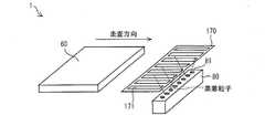
- FIG. 12is a side view illustrating a schematic configuration of a conventional vapor deposition apparatus 250
- FIG. 13is a perspective view illustrating a schematic configuration of a vapor deposition source 280, a vapor deposition source crucible 282, and a pipe 283 of the vapor deposition apparatus 250.
- the vapor deposition apparatus 250is an apparatus for forming a film on the deposition target substrate 260, and includes a shadow mask 270, a vapor deposition source 280, a vapor deposition source crucible 282, and a pipe 283.
- the shadow mask 270 and the vapor deposition source 280are disposed in the vacuum chamber 290, and the vapor deposition source crucible 282 is fixed to a support base (not shown).
- the vapor deposition source 280has a plurality of injection ports (nozzles) 281 for injecting vapor deposition particles, and the injection ports 281 are arranged in one row as shown in FIG.
- the vapor deposition source crucible 282stores a solid or liquid vapor deposition material.
- the vapor deposition materialis heated inside the vapor deposition source crucible 282 to be gaseous vapor particles, and is supplied (introduced) to the vapor deposition source 280 through the pipe 283.
- the pipe 283is connected to one end (supply side end) of the row of the injection ports 281 of the vapor deposition source 280, and the vapor deposition particles supplied to the vapor deposition source 280 are injected from the injection port 281. . Note that the pipe 283 is heated to a temperature at which vapor deposition particles do not adhere.
- the vapor deposition surface of the deposition target substrate 260 and the vapor deposition source 280are arranged to face each other.
- a shadow mask 270 having an opening corresponding to the pattern of the vapor deposition regionis closely fixed to the vapor deposition surface of the deposition target substrate 260 so that the vapor deposition particles do not adhere to a region other than the target vapor deposition region.
- the deposition target substrate 260 and the shadow mask 270are relatively moved (scanned) with respect to the vapor deposition source 280 while vapor deposition particles are ejected from the ejection port 281. Thereby, a predetermined pattern is formed on the deposition target substrate 260.
- Japanese Patent PublicationJapanese Patent Laid-Open No. 8-227276 (published on September 3, 1996)” Japanese Patent Publication “JP 2000-188179 A (published July 4, 2000)”
- the conventional technique as described abovehas a problem that the film thickness distribution of the deposited film becomes non-uniform.
- FIG. 14is a graph showing the relationship between the position of the deposition target substrate 260 along the arrangement direction of the injection ports 281 and the distribution (thickness) of vapor deposition particles.
- a position facing the supply side end of the vapor deposition source 280is A
- a position facing the end opposite to the supply side end of the vapor deposition source 280is B.
- the inside of the vapor deposition source 280is affected by the pressure difference in the supply path and the injection port, the internal shape, conductance, and the like, the amount of vapor deposition particles injected from each injection port 281 varies. Specifically, since the vapor deposition particles are sequentially injected from the injection port 281 near the supply side end portion, the density of the vapor deposition particles decreases as the distance from the supply side end portion increases, and a pressure difference is generated inside the vapor deposition source 280. Therefore, the larger the distance from the supply side end of the vapor deposition source 280, the smaller the injection amount of the vapor deposition particles from the injection port 281. Accordingly, as shown in FIG.
- the amount of vapor deposition particlesvaries depending on the position in the substrate surface for the vapor deposition film on the deposition target substrate 260 constituted by the synthesis of vapor deposition particles injected from various injection ports 281. Will be different. For this reason, nonuniformity of the film thickness distribution occurs in the substrate surface.
- the light emission characteristics of organic EL elementsare extremely sensitive to the film thickness of the deposited organic film, and the difference in film thickness of the organic film within the screen of the organic EL display device results in uneven display and uneven life characteristics. Connect directly. Therefore, it is desirable to deposit the light emitting layer of the organic EL element as uniformly as possible.
- the present inventionhas been made in view of the above problems, and an object thereof is to provide a vapor deposition apparatus and a vapor deposition method capable of depositing vapor deposition particles with a uniform film thickness on a deposition target substrate.
- a vapor deposition apparatusis a vapor deposition apparatus that forms a film on a deposition target substrate, and has a plurality of injection ports that eject vapor deposition particles to the deposition target substrate.
- a vapor deposition sourcein which the injection ports are arranged in one or a plurality of rows, a plurality of pipes connected to the vapor deposition source, and a vapor deposition particle supply for supplying the vapor deposition particles to the vapor deposition source through the plurality of pipes And at least one of the plurality of pipes is connected to one end side of the row of the injection ports in the vapor deposition source, and at least one of the plurality of pipes is connected to the injection port of the vapor deposition source. It is characterized by being connected to the other end side of the row.
- a vapor deposition methodis a vapor deposition method for forming a film on a deposition target substrate, which has a plurality of injection ports, and the injection ports are arranged in one or more rows.
- the vapor deposition sourceis supplied to the deposition target substrate from the injection port.
- the vapor deposition particlesare connected to the vapor deposition source via a pipe connected to the other end side of the row of the injection ports in the vapor deposition source.
- the vapor deposition particlesare supplied from the vapor deposition particle supply means to the vapor deposition source through a plurality of pipes, and are injected from the injection port onto the film formation substrate.
- first pipea pipe connected to one end side of the row of injection ports in the vapor deposition source
- second pipea pipe connected to the other end side of the row of injection ports in the vapor deposition source
- the injection amount of particlesdecreases monotonously.
- the film thickness distribution of the vapor deposition particles when the vapor deposition particles are supplied from the first pipe and the film thickness distribution of the vapor deposition particles when the vapor deposition particles are supplied from the second pipeare as follows. It becomes symmetric. Therefore, the film thickness distribution obtained by synthesizing these film thickness distributions is more uniform than the film thickness distribution when the vapor deposition is performed without rotating the vapor deposition source. Therefore, it is possible to provide a vapor deposition apparatus and a vapor deposition method capable of vapor deposition of vapor deposition particles with a uniform film thickness on a deposition target substrate.
- the organic electroluminescence display device manufacturing method of the present inventionincludes a TFT substrate / first electrode manufacturing step of forming a first electrode on a TFT substrate, and an organic layer on which an organic layer including at least a light emitting layer is deposited on the TFT substrate.
- An organic electroluminescence display devicecomprising: a vapor deposition step; a second electrode vapor deposition step of depositing a second electrode; and a sealing step of sealing an organic electroluminescence element including the organic layer and the second electrode with a sealing member.
- the organic layer or the likecan be formed with a uniform film thickness by the vapor deposition method of the present invention, an organic electroluminescence display device with little display unevenness can be provided.
- the vapor deposition apparatusis a vapor deposition apparatus that forms a film on a film formation substrate, and has a plurality of injection holes for injecting vapor deposition particles onto the film formation substrate.
- Vapor deposition sourcearranged in one or more rows, a plurality of pipes connected to the vapor deposition source, vapor deposition particle supply means for supplying the vapor deposition particles to the vapor deposition source via the plurality of pipes, Moving means for moving the deposition target substrate relative to the deposition source, and at least one of the plurality of pipes is connected to one end side of the row of the injection ports in the deposition source, At least one of the pipes is configured to be connected to the other end side of the row of the injection ports in the vapor deposition source.
- the vapor deposition method according to the present inventionis a vapor deposition method for forming a film on a deposition target substrate, wherein the vapor deposition source has a plurality of injection ports, and the injection ports are arranged in one or more rows.
- the injection portis configured to supply vapor deposition particles to the vapor deposition source through a pipe connected to one end side of the row of the injection ports in the source, and move the deposition target substrate relative to the vapor deposition source.
- the vapor deposition sourcewas connected to the other end side of the row of the injection ports in the vapor deposition source Secondly, the vapor deposition particles are supplied to the vapor deposition source via a pipe, and the vapor deposition particles are ejected from the injection port to the film deposition substrate while moving the film deposition substrate relative to the vapor deposition source. Injection process. Therefore, there is an effect that it is possible to provide a vapor deposition apparatus and a vapor deposition method capable of depositing vapor deposition particles with a uniform film thickness on a deposition target substrate.
- FIG. 8is a cross-sectional view taken along line AA of the TFT substrate in the organic EL display device shown in FIG.
- FIG. 1It is a perspective view which shows schematic structure of the vapor deposition source unit of the vapor deposition apparatus shown in FIG. It is a graph which shows the relationship between the position in the film-forming substrate along the sequence direction of the injection port of a vapor deposition source, and distribution (thickness) of vapor deposition particles.
- a method for manufacturing a bottom emission type organic EL display device for RGB full color display in which light is extracted from the TFT substrate sideis given as an example. explain.
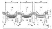
- FIG. 6is a sectional view showing a schematic configuration of an organic EL display device for RGB full-color display.
- 7is a plan view showing a configuration of a pixel constituting the organic EL display device shown in FIG. 6, and
- FIG. 8is a cross-sectional view taken along line AA of the TFT substrate in the organic EL display device shown in FIG. FIG.
- the organic EL display device 1 manufactured in the present embodimentincludes an organic EL element 20 connected to the TFT 12 and an adhesive layer on the TFT substrate 10 on which the TFT 12 (see FIG. 8) is provided. 30 and the sealing substrate 40 have the structure provided in this order.
- the organic EL element 20includes a pair of substrates (TFT substrates) by bonding the TFT substrate 10 on which the organic EL element 20 is laminated to a sealing substrate 40 using an adhesive layer 30. 10 and the sealing substrate 40).
- TFT substratessubstrates
- the organic EL element 20is sealed between the TFT substrate 10 and the sealing substrate 40 in this way, so that oxygen or moisture can enter the organic EL element 20 from the outside. It is prevented.
- the TFT substrate 10includes a transparent insulating substrate 11 such as a glass substrate as a supporting substrate.
- a plurality of wirings 14including a plurality of gate lines laid in the horizontal direction and a plurality of signal lines laid in the vertical direction and intersecting the gate lines are provided. It has been.
- a gate line driving circuit (not shown) for driving the gate lineis connected to the gate line, and a signal line driving circuit (not shown) for driving the signal line is connected to the signal line.
- the organic EL display device 1is a full-color active matrix organic EL display device, and red (R), green (G), and blue are respectively formed on the insulating substrate 11 in regions surrounded by the wirings 14.
- the sub-pixels 2R, 2G, and 2B of the respective colors including the organic EL elements 20 of the respective colors of (B)are arranged in a matrix.
- an area surrounded by these wirings 14is one sub pixel (dot), and R, G, and B light emitting areas are defined for each sub pixel.
- the pixel 2(that is, one pixel) has three sub-pixels: a red sub-pixel 2R that transmits red light, a green sub-pixel 2G that transmits green light, and a blue sub-pixel 2B that transmits blue light. It is composed of pixels 2R, 2G, and 2B.
- Each of the sub-pixels 2R, 2G, and 2Bincludes openings 15R and 15G that are covered by the light-emitting layers 23R, 23G, and 23B of the respective stripes as light-emitting regions of the respective colors that are responsible for light emission in the sub-pixels 2R, 2G, and 2B ⁇ 15B is provided.
- the light emitting layers 23R, 23G, and 23Bare patterned by vapor deposition for each color.
- the openings 15R, 15G, and 15Bwill be described later.
- These sub-pixels 2R, 2G, and 2Bare provided with TFTs 12 connected to the first electrode 21 in the organic EL element 20, respectively.
- the light emission intensity of each of the sub-pixels 2R, 2G, and 2Bis determined by scanning and selection by the wiring 14 and the TFT 12.
- the organic EL display device 1realizes image display by selectively causing the organic EL element 20 to emit light with desired luminance using the TFT 12.
- the TFT substrate 10will be described.
- the TFT substrate 10has a TFT 12 (switching element), an interlayer film 13 (interlayer insulating film, planarizing film), a wiring 14 and an edge cover 15 on a transparent insulating substrate 11 such as a glass substrate. It has the structure formed in this order.
- TFTs 12are provided corresponding to the sub-pixels 2R, 2G, and 2B, respectively.
- the structure of the TFTis conventionally well known. Therefore, illustration and description of each layer in the TFT 12 are omitted.
- the interlayer film 13is laminated on the insulating substrate 11 over the entire region of the insulating substrate 11 so as to cover the TFTs 12.
- the first electrode 21 in the organic EL element 20is formed on the interlayer film 13.
- the interlayer film 13is provided with a contact hole 13a for electrically connecting the first electrode 21 in the organic EL element 20 to the TFT 12.
- the TFT 12is electrically connected to the organic EL element 20 through the contact hole 13a.
- the edge cover 15prevents the first electrode 21 and the second electrode 26 in the organic EL element 20 from being short-circuited when the organic EL layer becomes thin or the electric field concentration occurs at the pattern end of the first electrode 21. It is an insulating layer for preventing.
- the edge cover 15is formed on the interlayer film 13 so as to cover the pattern end of the first electrode 21.
- the edge cover 15is provided with openings 15R, 15G, and 15B for each of the sub-pixels 2R, 2G, and 2B.
- the openings 15R, 15G, and 15B of the edge cover 15are light emitting areas of the sub-pixels 2R, 2G, and 2B.
- the sub-pixels 2R, 2G, and 2Bare partitioned by the edge cover 15 having an insulating property.
- the edge cover 15also functions as an element isolation film.
- the organic EL element 20is a light emitting element that can emit light with high luminance by low-voltage direct current drive, and a first electrode 21, an organic EL layer, and a second electrode 26 are laminated in this order.
- the first electrode 21is a layer having a function of injecting (supplying) holes into the organic EL layer. As described above, the first electrode 21 is connected to the TFT 12 via the contact hole 13a.
- a hole injection layer / hole transport layer 22As shown in FIG. 8, between the first electrode 21 and the second electrode 26, as an organic EL layer, from the first electrode 21 side, a hole injection layer / hole transport layer 22, and light emitting layers 23R, 23G, 23B, the electron carrying layer 24, and the electron injection layer 25 have the structure formed in this order.
- the stacking orderis that in which the first electrode 21 is an anode and the second electrode 26 is a cathode, the first electrode 21 is a cathode, and the second electrode 26 is an anode.
- the order of stackingis reversed.
- the hole injection layeris a layer having a function of increasing the efficiency of hole injection into the light emitting layers 23R, 23G, and 23B.
- the hole transport layeris a layer having a function of improving the efficiency of transporting holes to the light emitting layers 23R, 23G, and 23B.
- the hole injection layer / hole transport layer 22is uniformly formed on the entire display region of the TFT substrate 10 so as to cover the first electrode 21 and the edge cover 15.
- the hole injection layer / hole transport layer 22 in which the hole injection layer and the hole transport layer are integratedis provided as the hole injection layer and the hole transport layer.
- An examplewill be described.
- the present embodimentis not limited to this.
- the hole injection layer and the hole transport layermay be formed as independent layers.
- the light emitting layers 23R, 23G, and 23Bcorrespond to the sub-pixels 2R, 2G, and 2B so as to cover the openings 15R, 15G, and 15B of the edge cover 15, respectively. Is formed.
- the light emitting layers 23R, 23G, and 23Bare layers having a function of emitting light by recombining holes injected from the first electrode 21 side and electrons injected from the second electrode 26 side. .
- the light emitting layers 23R, 23G, and 23Bare each formed of a material having high light emission efficiency, such as a low molecular fluorescent dye or a metal complex.
- the electron transport layer 24is a layer having a function of increasing the electron transport efficiency from the second electrode 26 to the light emitting layers 23R, 23G, and 23B.
- the electron injection layer 25is a layer having a function of increasing the electron injection efficiency from the second electrode 26 to the light emitting layers 23R, 23G, and 23B.
- the electron transport layer 24is formed on the light emitting layer 23R / 23G / 23B and the hole injection layer / hole transport layer 22 so as to cover the light emitting layer 23R / 23G / 23B and the hole injection layer / hole transport layer 22.
- the TFT substrate 10is formed uniformly over the entire display area. Further, the electron injection layer 25 is uniformly formed on the entire surface of the display region of the TFT substrate 10 on the electron transport layer 24 so as to cover the electron transport layer 24.
- the electron transport layer 24 and the electron injection layer 25may be formed as independent layers as described above, or may be provided integrally with each other. That is, the organic EL display device 1 may include an electron transport layer / electron injection layer instead of the electron transport layer 24 and the electron injection layer 25.
- the second electrode 26is a layer having a function of injecting electrons into the organic EL layer composed of the organic layers as described above.
- the second electrode 26is uniformly formed on the entire surface of the display region of the TFT substrate 10 on the electron injection layer 25 so as to cover the electron injection layer 25.
- organic layers other than the light emitting layers 23R, 23G, and 23Bare not essential layers as the organic EL layer, and may be appropriately formed according to the required characteristics of the organic EL element 20.
- a carrier blocking layercan also be added to the organic EL layer as necessary. For example, by adding a hole blocking layer as a carrier blocking layer between the light emitting layers 23R, 23G, and 23B and the electron transport layer 24, the holes are prevented from falling out to the electron transport layer 24, and the light emission efficiency is improved. can do.
- First electrode / light emitting layer / second electrode(2) First electrode / hole transport layer / light emitting layer / electron transport layer / second electrode (3) First electrode / hole transport layer / light emitting layer / Hole blocking layer (carrier blocking layer) / electron transport layer / second electrode (4) first electrode / hole transport layer / light emitting layer / hole blocking layer / electron transport layer / electron injection layer / second electrode (5 ) 1st electrode / hole injection layer / hole transport layer / light emitting layer / electron transport layer / electron injection layer / second electrode (6) 1st electrode / hole injection layer / hole transport layer / light emitting layer / positive Hole blocking layer / electron transport layer / second electrode (7) first electrode / hole injection layer / hole transport layer / light emitting layer / hole blocking layer / electron transport layer / electron injection layer / second electrode (8) 1st electrode
- the configuration of the organic EL element 20is not limited to the above-described exemplary layer configuration, and a desired layer configuration can be adopted according to the required characteristics of the organic EL element 20 as described above.
- FIG. 9is a flowchart showing the manufacturing steps of the organic EL display device 1 in the order of steps.
- the manufacturing method of the organic EL display device 1includes, for example, a TFT substrate / first electrode manufacturing step (S1), a hole injection layer / hole transport layer deposition configuration (S2). ), A light emitting layer vapor deposition step (S3), an electron transport layer vapor deposition step (S4), an electron injection layer vapor deposition step (S5), a second electrode vapor deposition step (S6), and a sealing step (S7).
- the stacking order described in the present embodimentuses the first electrode 21 as an anode and the second electrode 26 as a cathode, and conversely, uses the first electrode 21 as a cathode and the second electrode 26. Is used as the anode, the stacking order of the organic EL layers is reversed. Similarly, the materials constituting the first electrode 21 and the second electrode 26 are also reversed.
- a photosensitive resinis applied on an insulating substrate 11 such as glass on which TFTs 12 and wirings 14 are formed by a known technique, and patterning is performed by a photolithography technique, thereby insulating substrate 11.
- An interlayer film 13is formed thereon.
- the insulating substrate 11has a thickness of 0.7 to 1.1 mm, a length in the y-axis direction (vertical length) of 400 to 500 mm, and a length in the x-axis direction (horizontal length) of 300.
- a glass substrate or a plastic substrate of ⁇ 400 mmis used. In this embodiment, a glass substrate is used.
- an acrylic resin or a polyimide resincan be used as the interlayer film 13.
- the acrylic resininclude Optomer series manufactured by JSR Corporation.
- a polyimide resinthe photo nice series by Toray Industries, Inc. is mentioned, for example.
- the polyimide resinis generally not transparent but colored. Therefore, as shown in FIG. 8, when a bottom emission type organic EL display device is manufactured as the organic EL display device 1, a transparent resin such as an acrylic resin is more preferably used as the interlayer film 13. Used.
- the film thickness of the interlayer film 13is not particularly limited as long as the step due to the TFT 12 can be compensated. In this embodiment, for example, the thickness is about 2 ⁇ m.
- a contact hole 13 a for electrically connecting the first electrode 21 to the TFT 12is formed in the interlayer film 13.
- an ITO (Indium Tin Oxide: Indium Tin Oxide) filmis formed with a thickness of 100 nm by a sputtering method or the like.
- the ITO filmis etched using ferric chloride as an etchant. Thereafter, the photoresist is stripped using a resist stripping solution, and substrate cleaning is further performed. Thereby, the first electrode 21 is formed in a matrix on the interlayer film 13.
- Examples of the conductive film material used for the first electrode 21include transparent conductive materials such as ITO, IZO (Indium (Zinc Oxide), gallium-doped zinc oxide (GZO), gold (Au), Metal materials such as nickel (Ni) and platinum (Pt) can be used.
- transparent conductive materialssuch as ITO, IZO (Indium (Zinc Oxide), gallium-doped zinc oxide (GZO), gold (Au), Metal materials such as nickel (Ni) and platinum (Pt) can be used.
- a method for laminating the conductive filmin addition to the sputtering method, a vacuum deposition method, a CVD (chemical vapor deposition) method, a plasma CVD method, a printing method, or the like can be used.
- the thickness of the first electrode 21is not particularly limited, but as described above, for example, the thickness can be set to 100 nm.
- the edge cover 15is patterned and formed with a film thickness of, for example, about 1 ⁇ m.
- the same insulating material as that of the interlayer film 13can be used.
- the TFT substrate 10 and the first electrode 21are produced (S1).
- the TFT substrate 10 that has undergone the above-described stepsis subjected to oxygen plasma treatment as a vacuum baking for dehydration and surface cleaning of the first electrode 21.
- a hole injection layer and a hole transport layerare displayed on the TFT substrate 10 on the TFT substrate 10 using a conventional vapor deposition apparatus. Vapor deposition is performed on the entire area (S2).
- an open mask having an entire display area openedis aligned and adhered to the TFT substrate 10 and then scattered from the deposition source while rotating the TFT substrate 10 and the open mask together. Vapor deposition particles are uniformly deposited on the entire display region through the opening of the open mask.
- vapor deposition on the entire surface of the display areameans that vapor deposition is performed continuously between adjacent sub-pixels of different colors.
- Examples of the material for the hole injection layer and the hole transport layerinclude benzine, styrylamine, triphenylamine, porphyrin, triazole, imidazole, oxadiazole, polyarylalkane, phenylenediamine, arylamine, oxazole, anthracene, and fluorenone. , Hydrazone, stilbene, triphenylene, azatriphenylene, and derivatives thereof, polysilane compounds, vinylcarbazole compounds, thiophene compounds, aniline compounds, etc., heterocyclic or chain conjugated monomers, oligomers, or polymers Etc.
- the hole injection layer and the hole transport layermay be integrated as described above, or may be formed as independent layers.
- Each film thicknessis, for example, 10 to 100 nm.
- the hole injection layer / hole transport layer 22is provided as the hole injection layer and the hole transport layer, and the material of the hole injection layer / hole transport layer 22 is 4,4′-bis [ N- (1-naphthyl) -N-phenylamino] biphenyl ( ⁇ -NPD) was used.
- the film thickness of the hole injection layer / hole transport layer 22was 30 nm.
- the light emitting layers 23R, 23G, and 23B corresponding to the sub-pixels 2R, 2G, and 2B so as to cover the openings 15R, 15G, and 15B of the edge cover 15.are separately formed (pattern formation) (S3).
- the light emitting layers 23R, 23G, and 23Bare made of a material having high light emission efficiency such as a low molecular fluorescent dye or a metal complex.
- Examples of materials for the light emitting layers 23R, 23G, and 23Binclude anthracene, naphthalene, indene, phenanthrene, pyrene, naphthacene, triphenylene, anthracene, perylene, picene, fluoranthene, acephenanthrylene, pentaphen, pentacene, coronene, butadiene, and coumarin.
- the film thickness of the light emitting layers 23R, 23G, and 23Bis, for example, 10 to 100 nm.
- the vapor deposition method and the vapor deposition apparatus according to the present embodimentcan be particularly preferably used for such separate formation (pattern formation) of the light emitting layers 23R, 23G, and 23B.
- the electron transport layer 24, the hole injection layer / hole transport layer 22 and the light emitting layers 23R, 23G, and 23Bare formed.
- the entire surface of the display area of the TFT substrate 10is deposited so as to cover (S4).
- the electron injection layer 25is formed on the entire surface of the display region of the TFT substrate 10 so as to cover the electron transport layer 24 by the same method as the hole injection layer / hole transport layer deposition step (S2). Evaporation is performed (S5).
- Examples of the material for the electron transport layer 24 and the electron injection layer 25include tris (8-quinolinolato) aluminum complex, oxadiazole derivative, triazole derivative, phenylquinoxaline derivative, silole derivative and the like.
- Alqtris (8-hydroxyquinoline) aluminum
- anthracenenaphthalene
- phenanthrenepyrene
- anthraceneperylene
- butadienecoumarin
- acridinestilbene
- 1,10-phenanthrolineand derivatives and metal complexes thereof
- the electron transport layer 24 and the electron injection layer 25may be integrated or formed as independent layers.
- Each film thicknessis, for example, 1 to 100 nm.
- the total film thickness of the electron transport layer 24 and the electron injection layer 25is, for example, 20 to 200 nm.
- Alqis used as the material of the electron transport layer 24, and LiF is used as the material of the electron injection layer 25.
- the thickness of the electron transport layer 24was 30 nm, and the thickness of the electron injection layer 25 was 1 nm.
- the second electrode 26is applied to the entire display region of the TFT substrate 10 so as to cover the electron injection layer 25 by the same method as the hole injection layer / hole transport layer deposition step (S2). Evaporation is performed (S6).
- Electrode material of the second electrode 26a metal having a small work function is preferably used.
- examples of such electrode materialsinclude magnesium alloys (MgAg, etc.), aluminum alloys (AlLi, AlCa, AlMg, etc.), metallic calcium, and the like.
- the thickness of the second electrode 26is, for example, 50 to 100 nm.
- the organic EL element 20 including the organic EL layer, the first electrode 21, and the second electrode 26was formed on the TFT substrate 10.
- the TFT substrate 10 on which the organic EL element 20 was formed and the sealing substrate 40were bonded together with an adhesive layer 30 to encapsulate the organic EL element 20.
- sealing substrate 40for example, an insulating substrate such as a glass substrate or a plastic substrate having a thickness of 0.4 to 1.1 mm is used. In this embodiment, a glass substrate is used.
- the vertical length and the horizontal length of the sealing substrate 40may be appropriately adjusted according to the size of the target organic EL display device 1, and an insulating substrate having substantially the same size as the insulating substrate 11 in the TFT substrate 10 is used. After sealing the organic EL element 20, the organic EL element 20 may be divided according to the size of the target organic EL display device 1.
- sealing method of the organic EL element 20it is not limited to an above-described method.
- Other sealing methodsinclude, for example, a method in which engraved glass is used as the sealing substrate 40 and sealing is performed in a frame shape with a sealing resin, frit glass, or the like, or between the TFT substrate 10 and the sealing substrate 40.
- a method of filling a resin in betweenThe manufacturing method of the organic EL display device 1 does not depend on the sealing method, and any sealing method can be applied.
- a protective film(not shown) that prevents oxygen and moisture from entering the organic EL element 20 from the outside is provided on the second electrode 26 so as to cover the second electrode 26. Good.
- the protective filmis made of an insulating or conductive material. Examples of such a material include silicon nitride and silicon oxide. Further, the thickness of the protective film is, for example, 100 to 1000 nm.
- the organic EL display device 1is completed through the above steps.
- a predetermined imageis displayed by controlling the light emission luminance of each of the sub-pixels 2R, 2G, and 2B.
- FIG. 1is a side view showing a configuration of a vapor deposition apparatus 50 according to the present embodiment.
- the vapor deposition device 50is a device that forms a film on the deposition target substrate 60, and includes a shadow mask 70, a vapor deposition source 80, a vapor deposition source crucible 82, and two pipes 83a and 83b.
- the shadow mask 70 and the vapor deposition source 80are disposed in the vacuum chamber 90, and the vapor deposition source crucible 82 is fixed to a support base (not shown).
- the structures of the film formation substrate 60, the shadow mask 70, and the vapor deposition source crucible 82are the same as those of the film formation substrate 260, the shadow mask 270, and the vapor deposition source crucible 282 shown in FIG.
- the vapor deposition source 80has a plurality of ejection ports 81 through which vapor deposition particles are ejected, and the ejection ports 81 are arranged in a row as shown in FIG.
- the vapor deposition source crucible 82stores a solid or liquid vapor deposition material. Further, the vapor deposition source crucible 82 is arranged outside the vacuum chamber 90. Thereby, it is not necessary to open the vacuum chamber 90 to the atmosphere each time the vapor deposition material is supplied to the vapor deposition source crucible 82, and the throughput can be improved. Further, a space can be provided in the vacuum chamber 90, and the design in the vacuum chamber 90 is facilitated.
- the vapor deposition materialis heated inside the vapor deposition source crucible 82 to become gaseous vapor deposition particles, and is supplied (introduced) to the vapor deposition source 80 through the pipes 83a and 83b.
- One pipe 83 ais connected to one end face (referred to as “supply-side end face a”) of the row of the injection ports 81 of the vapor deposition source 80, and the other pipe 83 b is the injection port 81 of the vapor deposition source 80.
- supply-side end face bare connected to the other end surface (referred to as “supply-side end surface b”).
- the vapor deposition particles supplied to the vapor deposition source 80are ejected from the ejection port 81.
- the vapor deposition surface of the deposition target substrate 60 and the vapor deposition source 80are arranged to face each other.
- a shadow mask 70 having an opening corresponding to the pattern of the vapor deposition regionis closely fixed to the vapor deposition surface of the deposition target substrate 60 so that the vapor deposition particles do not adhere to a region other than the target vapor deposition region. Then, the deposition target substrate 60 and the shadow mask 70 are moved relative to the deposition source 80 (scanned) by a moving unit (not shown) while ejecting the deposition particles from the injection port 81.
- the moving meansmoves the film formation substrate 60 and the shadow mask 70 in a direction perpendicular to the arrangement direction of the injection ports 81 ( It is reciprocated in the direction from the back side to the front side in the drawing and the opposite direction. As a result, a predetermined pattern is formed on the deposition target substrate 60.
- a pipe 283 for supplying vapor deposition particlesis connected only to one end face of the row of the injection ports 281 of the vapor deposition source 280.
- the pipe 83ais connected to the end face on one end side of the row of the injection ports 81 of the vapor deposition source 80, and the other side of the row of the injection ports 81 of the vapor deposition source 80. It differs from the conventional vapor deposition apparatus 250 in that the pipe 83b is also connected to the end face on the end side.
- the pipes 83a and 83bare provided with valves 84a and 84b (supply control means), respectively.
- the valves 84a and 84bcontrol the supply amount of the vapor deposition particles to the vapor deposition source 80 by opening and closing the internal paths of the pipes 83a and 83b, respectively.
- the valve 84ais open, the vapor deposition particles pass through the introduction path P1 indicated by the solid line arrow, and when the valve 84b is open, the vapor deposition particles pass through the introduction path P2 indicated by the broken line arrow.
- the introduction pathis switched according to the scanning direction of the film formation substrate 60. Specifically, first, the valve 84a is opened, the vapor deposition particles are supplied to the vapor deposition source 80 through the pipe 83a, and the film formation substrate 60 is scanned in the back direction (the forward direction) in FIG. The vapor deposition particles are injected from 81 to the deposition target substrate 60 (first injection step). At this time, the valve 84b is closed.
- the valve 84aWhen scanning in the forward direction ends (that is, when the deposition target substrate 60 reaches a position not facing the vapor deposition source 80), the valve 84a is closed, and the supply of vapor deposition particles from the pipe 83a is terminated. Subsequently, the valve 84b is opened, the vapor deposition particles are supplied to the vapor deposition source 80 via the pipe 83b, and the film deposition substrate 60 is scanned from the injection port 81 while scanning in the forward direction (return direction) in FIG. The vapor deposition particles are injected onto the film formation substrate 60 (second injection step). When the scanning in the backward direction is finished, the ejection of the vapor deposition particles is finished.
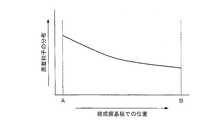
- FIG. 3is a graph showing the relationship between the position of the deposition target substrate 60 along the arrangement direction of the injection ports 81 and the distribution (thickness) of vapor deposition particles.
- the position facing the supply side end face a of the vapor deposition source 80 in the state of FIG. 1is A
- the position facing the supply side end face b of the vapor deposition source 80is B.
- the solid lineindicates the distribution of vapor deposition particles when the film formation substrate 60 is scanned in the forward direction
- the broken lineindicates the distribution of vapor deposition particles when the film formation substrate 60 is scanned in the double path direction.
- the alternate long and short dash lineindicates the distribution of the vapor deposition particles when the reciprocating scanning is completed.
- the amount of vapor deposition particles emitted from the injection port 81decreases as the distance from the supply side end surface of the vapor deposition source 80 increases. Therefore, the distribution of the vapor deposition particles when the deposition target substrate 60 is scanned in the forward direction (that is, when vapor deposition particles are supplied to the vapor deposition source 80 via the pipe 83a) is from the position A as indicated by the solid line. It gradually decreases toward B.
- the vapor deposition particlesare supplied to the vapor deposition source 80 via the pipe 83b.
- the distribution of the injection amount of the vapor deposition particles injected onto the film formation substrate 60is also reversed.
- the film thickness distribution when the deposition target substrate 60 scans in the backward directionis symmetric with respect to the film thickness distribution indicated by the solid line with respect to the intermediate position between the position A and the position B.
- the film thickness distribution at the time when the reciprocating scan of the deposition target substrate 60 is completedis the sum of the film thickness distribution indicated by the solid line and the film thickness distribution indicated by the broken line. Therefore, as shown by the alternate long and short dash line, the film thickness distribution is uniform when compared with the film thickness distribution when scanned in the forward direction and the film thickness distribution when scanned in the backward direction.
- the opening / closing switching of the valves 84a and 84bdoes not need to be performed every time the scanning direction of the deposition target substrate 60 is switched. For example, the film formation substrate 60 is reciprocated three times with the valve 84b closed and the valve 84a opened, and then the film formation substrate 60 is reciprocated three times with the valve 84a closed and the valve 84b opened. May be. Further, the switching of the valves 84 a and 84 b is performed when the deposition target substrate 60 passes over the deposition source 80 and is in a position where the deposition particles do not reach the deposition target substrate 60.
- valves 84a and 84bare opened, the amount of vapor deposition particles supplied from the respective pipes 83a and 83b to the vapor deposition source 80 changes due to a subtle difference in shape and conductance between the pipe 83a and the pipe 83b.
- the pressure distribution in the source 80is also complicated, and it is difficult to make the film thickness distribution uniform. Therefore, it is preferable that the valves 84a and 84b are controlled so that both do not open simultaneously. However, if the influence of the pipes 83a and 83b is very small, both the valves 84a and 84b can be opened.
- the pipes 83a and 83bare connected to the end faces on the one end side and the other end side of the row of the injection ports 81 of the vapor deposition source 80.
- the positions where the pipes 83a and 83b are connectedare not limited thereto. .
- pipes 83a and 83bmay be connected to the vicinity of the end of the row of the injection ports 81 on the side surface in the longitudinal direction of the vapor deposition source 80A.
- FIG. 4Bin the vapor deposition source 80A having a plurality of rows of injection ports 81, it is preferable to connect a plurality of pipes to each end face.
- two pipes 83a and 83care connected to the end surface on one end side of the row of the injection ports 81 of the vapor deposition source 80A, and the end surface on the other end side of the row of the injection ports 81 of the vapor deposition source 80A.
- two pipes 83b and 83dare connected. Thereby, the nonuniformity of the injection quantity for every row
- the opening of the valves 84a and 84c of the pipes 83a and 83c and the opening of the valves 84b and 84d of the pipes 83b and 83dare alternately switched according to the switching in the scanning direction of the film formation substrate 60.
- the valves 83a and 84c of the pipes 83a and 83care opened, and the valves 83b and 84d of the pipes 83b and 83d are closed, while the deposition target substrate 60 is scanned in the forward direction, the pipes 83a and 83c.
- the vapor deposition particlesare supplied to the vapor deposition source 80, and the vapor deposition particles are ejected from the injection port 81 to the film formation substrate 60.
- valves 84 a and 84 care closed, the valves 84 b and 84 d are opened, and the deposition particles are supplied to the deposition source 80 through the pipes 83 b and 83 d while scanning the deposition target substrate 60 in the backward direction.
- the vapor deposition particlesare injected from 81 to the deposition target substrate 60.
- pipingis connected to one end side and the other end side of the row of injection ports in the vapor deposition source, but the position where the piping is connected is not limited to this.
- the injection ports 81are arranged in a matrix like the vapor deposition source 80B shown in FIG. 4C, pipes may be connected to the four sides of the vapor deposition source 80B.
- pipes 83a and 83bare respectively connected to one end side and the other end side of the row of the injection ports 81 in the vapor deposition source 80B.
- Pipes 83e and 83fare connected to one end side and the other end side of the row of injection ports 81 at 80B, respectively.
- valves 84a, 84b, 84e, and 84f of the pipes 83a, 83b, 83e, and 83fmay be sequentially opened in accordance with switching in the scanning direction of the deposition target substrate 60, or all the valves 84a, 84b may be opened. -84e and 84f may be opened simultaneously.
- the deposition substrate and the shadow maskare in close contact with each other.
- vapor depositionmay be performed by providing a gap between the deposition substrate and the shadow mask.
- a shadow mask that covers the entire surface of the deposition target substrateis used, but the present invention is not limited to this.
- a shadow mask 170 having a smaller area than the vapor deposition region of the deposition target substrate 60may be used as the shadow mask.
- the relative position between the shadow mask 170 and the vapor deposition source 80is fixed, and alignment is performed so that the shadow mask 170 faces the deposition target substrate with a certain gap. Then, the film formation substrate 60 is moved relative to the shadow mask 170 and the vapor deposition source 80, and vapor deposition particles are sequentially vapor deposited on the vapor deposition region of the film deposition substrate 60 through the opening 171 of the shadow mask 170.
- FIG. 10is a side view showing the configuration of the vapor deposition apparatus 150 according to the present embodiment.
- the vapor deposition apparatus 150is the structure further provided with the auxiliary piping 83g in the vapor deposition apparatus 50 shown in FIG.
- the auxiliary piping 83gis connected to an intermediate portion of the array of the injection ports 81 in the vapor deposition source 80.
- the vapor deposition source crucible 82supplies vapor deposition particles to the vapor deposition source 80 via the pipes 83a and 83b and the auxiliary pipe 83g. That is, the vapor deposition particles are supplied to the vapor deposition source 80 from the introduction path P3 indicated by the one-dot chain line in addition to the introduction paths P1 and P2.
- auxiliary piping 83gis not provided with a valve. That is, vapor deposition particles are supplied to the vapor deposition source 80 from the auxiliary pipe 83g regardless of the scanning direction of the film formation substrate 60.
- the procedure of the vapor deposition processis the same as that in the first embodiment. Thereby, the vapor deposition apparatus 150 concerning this Embodiment can acquire the effect similar to the vapor deposition apparatus 50 concerning Embodiment 1.
- the auxiliary pipe 83gis provided, so that the film thickness distribution of the vapor deposition particles can be made more uniform. This will be described with reference to FIG.
- FIG. 11is a graph showing the relationship between the position of the deposition target substrate 60 along the arrangement direction of the injection ports 81 and the distribution (thickness) of vapor deposition particles.
- the solid lineindicates the distribution of vapor deposition particles when the film formation substrate 60 is scanned in the forward direction
- the broken lineindicates the distribution of vapor deposition particles when the film formation substrate 60 is scanned in the double path direction.
- the alternate long and short dash lineindicates the distribution of the vapor deposition particles when the reciprocating scanning is completed.
- the film thickness in the vicinity of the intermediate positionis convex.
- the film thickness distribution of vapor deposition particlecan be made more uniform compared with the film thickness distribution in the said Embodiment 1.
- auxiliary pipeis connected to a portion other than one end and the other end of the row of injection ports in the vapor deposition source.
- auxiliary pipe 83gmay include a valve.
- a line type vapor deposition source in which injection ports are arranged in one rowis used as the vapor deposition source.
- a surface type vapor deposition source in which a plurality of rows of injection ports are arrangedmay be used.
- pipesare respectively connected to one end surface and the other end surface of the row of injection ports in the vapor deposition source.
- depositionmay be performed without moving the deposition target substrate relative to the deposition source.
- the arrangement direction of the injection portsis perpendicular to the scanning direction of the film formation substrate, but may be slightly deviated from the direction perpendicular to the scanning direction of the film formation substrate.
- the shape of the injection portis a point shape, but is not limited thereto, and may be, for example, a slit shape that is long in the arrangement direction of the injection ports.
- the present inventioncan also be applied to a contact-type scan vapor deposition method in which a film formation substrate is slid and vapor-deposited while the film formation substrate and a shadow mask are in close contact with each other. Further, the present invention can also be applied to the case where the deposition is performed on the entire surface of the deposition target substrate without using the shadow mask in which the opening pattern is formed for each sub-pixel as in S2 and S4 to S6 of FIG.
- the present inventioncan be applied not only to the deposition of an organic film but also to the deposition of a second electrode and the deposition of a sealing film.
- the variation in the thickness of the organic filmgreatly affects the characteristics of the organic EL display device, the application effect of the present invention is high.
- the film thickness variation of the second electrodeaffects the variation of electric resistance
- the variation of the sealing filmaffects the variation of moisture permeability and oxygen transmission rate. If the influence of these variations on the characteristics of the organic EL element is slight, the present invention may be applied only to the deposition of an organic film in view of the increase in equipment cost accompanying the complexity of the structure of the deposition apparatus. .
- a vapor deposition apparatusis a vapor deposition apparatus that forms a film on a deposition target substrate, and includes a plurality of injection ports that eject vapor deposition particles onto the deposition target substrate.
- a vapor deposition sourcein which the injection ports are arranged in one or a plurality of rows, a plurality of pipes connected to the vapor deposition source, and a vapor deposition particle supply for supplying the vapor deposition particles to the vapor deposition source via the plurality of pipes And at least one of the plurality of pipes is connected to one end side of the row of the injection ports in the vapor deposition source, and at least one of the plurality of pipes is connected to the injection port of the vapor deposition source Connected to the other end of the row.
- the vapor deposition method according to the embodiment of the present inventionis a vapor deposition method for forming a film on a deposition target substrate, and has a plurality of injection ports, and the injection ports are arranged in one or a plurality of rows.
- the vapor deposition sourceis supplied to the deposition target substrate from the injection port.
- the vapor deposition particlesare connected to the vapor deposition source via a pipe connected to the other end side of the row of the injection ports in the vapor deposition source.
- the vapor deposition particlesare supplied from the vapor deposition particle supply means to the vapor deposition source through a plurality of pipes, and are injected from the injection port onto the film formation substrate.
- first pipea pipe connected to one end side of the row of injection ports in the vapor deposition source
- second pipea pipe connected to the other end side of the row of injection ports in the vapor deposition source
- the injection amount of particlesdecreases monotonously.
- the film thickness distribution of the vapor deposition particles when the vapor deposition particles are supplied from the first pipe and the film thickness distribution of the vapor deposition particles when the vapor deposition particles are supplied from the second pipeare as follows. It becomes symmetric. Therefore, the film thickness distribution obtained by synthesizing these film thickness distributions is more uniform than the film thickness distribution when the vapor deposition is performed without rotating the vapor deposition source. Therefore, it is possible to provide a vapor deposition apparatus and a vapor deposition method capable of vapor deposition of vapor deposition particles with a uniform film thickness on a deposition target substrate.
- each pipepreferably includes supply control means for controlling the supply amount of the vapor deposition particles to the vapor deposition source.
- the supply control meanscan switch ON / OFF the supply of vapor deposition particles from each pipe.
- vapor deposition particlescan be vapor-deposited with a more uniform film thickness by switching the piping which supplies vapor deposition particles according to the switching of the relative movement direction of a film-forming substrate.
- the vapor deposition particlesare supplied from any one of the plurality of pipes to the vapor deposition source when the vapor deposition particles are injected.
- a plurality of pipesare connected to the one end side and the other end side, respectively.
- the injection portsare arranged in a matrix, and at least one of the plurality of pipes is connected to one end side of the row of the injection ports in the vapor deposition source, It is preferable that at least one of the plurality of pipes is connected to the other end side of the row of the injection ports in the vapor deposition source.
- the film thickness distribution in the row direction of the injection portcan be made uniform.
- the vapor deposition apparatusin addition to the plurality of pipes, the vapor deposition apparatus further includes an auxiliary pipe, and the vapor deposition particle supplying unit includes the vapor deposition particles via the plurality of pipes and the auxiliary pipe. Is preferably supplied to the vapor deposition source, and the auxiliary pipe is connected to a portion other than the one end and the other end of the vapor deposition source.
- the auxiliary pipeis connected to an intermediate portion of the array of the injection ports in the vapor deposition source.
- the vapor deposition apparatuspreferably includes a moving means for moving the film formation substrate relative to the vapor deposition source.
- the arrangement direction of the plurality of injection portsis perpendicular to the direction in which the deposition target substrate is relatively moved.
- An organic electroluminescence display device manufacturing methodincludes a TFT substrate / first electrode manufacturing step of manufacturing a first electrode on a TFT substrate, and an organic layer including at least a light emitting layer on the TFT substrate.
- An organic layer deposition step for depositing the organic layera second electrode deposition step for depositing the second electrode, and a sealing step for sealing the organic electroluminescence element including the organic layer and the second electrode with a sealing member.
- a second injection stepis included.
- an organic layer or the likecan be formed with a uniform film thickness by the vapor deposition method according to the embodiment of the present invention, so that an organic electroluminescence display device with little display unevenness can be provided. it can.
- the present inventioncan be applied not only to vapor deposition of vapor deposition particles in the manufacture of an organic EL display device but also to vapor deposition of vapor deposition particles to any film formation target.
- Organic EL display device(Organic electroluminescence display device) 2 pixel 2B sub pixel 2G sub pixel 2R sub pixel 10 TFT substrate 11 insulating substrate 12 TFT 13 Interlayer film 13a Contact hole 14 Wiring 15 Edge cover 15R Opening 15G Opening 15B Opening 20 Organic EL element 21 First electrode 22 Hole injection layer / hole transporting layer 23R Light emitting layer 23G Light emitting layer 23B Light emitting layer 24 Electron transport layer 25 Electron injection layer 26 Second electrode 30 Adhesive layer 40 Sealing substrate 50 Deposition device 60 Deposition substrate 70 Shadow mask 80 Deposition source 80A Deposition source 80B Deposition source 81 Injection port 82 Deposition source crucible (deposition particle supply means) 83a piping 83b piping 83c piping 83b piping 83d piping 83e piping 83f piping 83g auxiliary piping 84a valve (supply control means) 84b Valve (supply control means) 84c Valve (supply control means) 84d valve (suppl
Landscapes
- Chemical & Material Sciences (AREA)
- Engineering & Computer Science (AREA)
- Manufacturing & Machinery (AREA)
- Chemical Kinetics & Catalysis (AREA)
- Materials Engineering (AREA)
- Mechanical Engineering (AREA)
- Metallurgy (AREA)
- Organic Chemistry (AREA)
- Physics & Mathematics (AREA)
- Optics & Photonics (AREA)
- Electroluminescent Light Sources (AREA)
- Physical Vapour Deposition (AREA)
Abstract
Description
Translated fromJapanese本発明は、真空蒸着法を用いた蒸着装置、蒸着方法、並びに、この蒸着装置および蒸着方法を用いた有機エレクトロルミネッセンス表示装置の製造方法に関する。The present invention relates to a vapor deposition apparatus using a vacuum vapor deposition method, a vapor deposition method, and a method for manufacturing an organic electroluminescence display device using the vapor deposition apparatus and the vapor deposition method.
近年、様々な商品や分野でフラットパネルディスプレイが活用されており、フラットパネルディスプレイのさらなる大型化、高画質化、低消費電力化が求められている。In recent years, flat panel displays have been used in various products and fields, and further flat panel displays are required to have larger sizes, higher image quality, and lower power consumption.
そのような状況下、有機材料の電界発光(Electroluminescence:以下、「EL」と記す)を利用した有機EL素子を備えた有機EL表示装置は、全固体型で、低電圧駆動、高速応答性、自発光性等の点で優れたフラットパネルディスプレイとして、高い注目を浴びている。Under such circumstances, an organic EL display device including an organic EL element using electroluminescence (hereinafter referred to as “EL”) of an organic material is an all-solid-state type, low voltage driving, high-speed response, As a flat panel display excellent in terms of self-luminous property and the like, it is attracting a great deal of attention.
有機EL表示装置は、例えば、TFT(薄膜トランジスタ)が設けられたガラス基板等からなる基板上に、TFTに接続された有機EL素子が設けられた構成を有している。The organic EL display device has, for example, a configuration in which an organic EL element connected to a TFT is provided on a substrate made of a glass substrate or the like provided with a TFT (thin film transistor).
有機EL素子は、低電圧直流駆動による高輝度発光が可能な発光素子であり、第1電極、有機EL層、および第2電極が、この順に積層された構造を有している。そのうち、第1電極はTFTと接続されている。また、第1電極と第2電極との間には、上記有機EL層として、正孔注入層、正孔輸送層、電子ブロッキング層、発光層、正孔ブロッキング層、電子輸送層、電子注入層等を積層させた有機層が設けられている。The organic EL element is a light emitting element that can emit light with high luminance by low-voltage direct current drive, and has a structure in which a first electrode, an organic EL layer, and a second electrode are stacked in this order. Of these, the first electrode is connected to the TFT. In addition, between the first electrode and the second electrode, as the organic EL layer, a hole injection layer, a hole transport layer, an electron blocking layer, a light emitting layer, a hole blocking layer, an electron transport layer, an electron injection layer The organic layer which laminated | stacked etc. is provided.
フルカラーの有機EL表示装置では、一般的に、赤(R)、緑(G)、青(B)の各色の発光層を備えた有機EL素子がサブ画素として基板上に配列形成される。TFTを用いて、これら有機EL素子を選択的に所望の輝度で発光させることによりカラー画像表示を行う。In a full-color organic EL display device, generally, organic EL elements including light emitting layers of red (R), green (G), and blue (B) are arranged and formed on a substrate as sub-pixels. A color image is displayed by selectively emitting light from these organic EL elements with a desired luminance using TFTs.
有機EL表示装置を製造するためには、各色に発光する有機発光材料からなる発光層を有機EL素子ごとに所定パターンで形成する必要がある。また、有機EL素子ごとにパターン形成が必要ない層については、有機EL素子で構成される画素領域全面に対して、一括して薄膜形成を行う。In order to manufacture an organic EL display device, it is necessary to form a light emitting layer made of an organic light emitting material that emits light of each color in a predetermined pattern for each organic EL element. In addition, for a layer that does not require pattern formation for each organic EL element, a thin film is collectively formed on the entire pixel region constituted by the organic EL element.
発光層を所定パターンで形成する方法としては、例えば、真空蒸着法、インクジェット法、レーザ転写法が知られている。例えば、低分子型有機EL表示装置(OLED)では、真空蒸着法が用いられることが多い(例えば、特許文献1および2)。As a method for forming the light emitting layer in a predetermined pattern, for example, a vacuum deposition method, an ink jet method, and a laser transfer method are known. For example, in a low molecular organic EL display (OLED), a vacuum deposition method is often used (for example,
真空蒸着法では、所定パターンの開口が形成されたマスク(蒸着マスクまたはシャドウマスクとも称される)が使用される。マスクが密着固定された基板の被蒸着面を蒸着源に対向させる。そして、蒸着源からの蒸着粒子(成膜材料)を、マスクの開口を通して被蒸着面に蒸着させることにより、所定パターンの薄膜が形成される。蒸着は発光層の色ごとに行われる(これを「塗り分け蒸着」という)。In the vacuum deposition method, a mask (also referred to as a deposition mask or a shadow mask) in which openings having a predetermined pattern are formed is used. The deposition surface of the substrate to which the mask is closely fixed is opposed to the deposition source. Then, vapor deposition particles (film forming material) from the vapor deposition source are vapor deposited on the vapor deposition surface through the opening of the mask, thereby forming a thin film having a predetermined pattern. Vapor deposition is performed for each color of the light emitting layer (this is called “separate vapor deposition”).
ここで、真空蒸着法を用いた従来の蒸着装置の構成を、図12および図13に基づいて説明する。Here, the configuration of a conventional vapor deposition apparatus using a vacuum vapor deposition method will be described with reference to FIGS.
図12は、従来の蒸着装置250の概略構成を示す側面図であり、図13は、蒸着装置250の蒸着源280、蒸着源坩堝282および配管283の概略構成を示す斜視図である。FIG. 12 is a side view illustrating a schematic configuration of a conventional
図12に示すように、蒸着装置250は、被成膜基板260に成膜を行う装置であり、シャドウマスク270、蒸着源280、蒸着源坩堝282および配管283を備えている。シャドウマスク270および蒸着源280は、真空チャンバ290内に配置され、蒸着源坩堝282は、図示しない支持台に固定されている。As shown in FIG. 12, the
蒸着源280は、蒸着粒子を射出する複数の射出口(ノズル)281を有しており、図13に示すように、射出口281は、1列に配置されている。The
蒸着源坩堝282には、固体または液体の蒸着材料が貯留されている。蒸着材料は、蒸着源坩堝282内部で加熱されて気体の蒸着粒子となり、配管283を通って蒸着源280に供給(導入)される。配管283は、蒸着源280の射出口281の列の一方端側の端部(供給側端部)に接続されており、蒸着源280に供給された蒸着粒子は、射出口281から射出される。なお、配管283は、蒸着粒子が付着しないような温度に加熱されている。The vapor deposition source crucible 282 stores a solid or liquid vapor deposition material. The vapor deposition material is heated inside the vapor
被成膜基板260の蒸着面と蒸着源280とは対向配置されている。目的とする蒸着領域以外の領域に蒸着粒子が付着しないように、蒸着領域のパターンに対応した開口部を有するシャドウマスク270が、被成膜基板260の蒸着面に密着固定されている。The vapor deposition surface of the
上記の構成において、射出口281から蒸着粒子を射出させながら、被成膜基板260およびシャドウマスク270を蒸着源280に対して相対移動(走査)させる。これにより、被成膜基板260に所定のパターンが形成される。In the above configuration, the
しかしながら、上述のような従来技術は、蒸着膜の膜厚分布が不均一になるという問題がある。However, the conventional technique as described above has a problem that the film thickness distribution of the deposited film becomes non-uniform.
図14は、射出口281の配列方向に沿った被成膜基板260での位置と、蒸着粒子の分布(厚さ)との関係を示すグラフである。このグラフでは、蒸着源280の供給側端部に対向する位置をAとし、蒸着源280の供給側端部の反対側の端部に対向する位置をBとしている。FIG. 14 is a graph showing the relationship between the position of the
蒸着源280の内部では、供給経路内および射出口内の圧力差、内部形状、コンダクタンス等の影響を受けるため、各射出口281から射出される蒸着粒子の量が異なってくる。具体的には、供給側端部に近い射出口281から順に蒸着粒子が射出されるため、供給側端部から離れるほど蒸着粒子の密度が低くなり、蒸着源280の内部で圧力差が生じる。そのため、蒸着源280の供給側端部からの距離が大きいほど、射出口281からの蒸着粒子の射出量が減少する。それに伴い、様々な射出口281から射出された蒸着粒子の合成によって構成される被成膜基板260上の蒸着膜についても、図14に示すように、基板面内の位置によって、蒸着粒子の量が異なってくる。このため、基板面内で膜厚分布の不均一が生じてしまう。Since the inside of the
特に、有機EL素子の発光特性は、蒸着される有機膜の膜厚に極めて敏感であり、有機EL表示装置の画面内での有機膜の膜厚差は、表示ムラや寿命特性の不均一に直結する。そのため、有機EL素子の発光層は、極力均一に蒸着することが望ましい。In particular, the light emission characteristics of organic EL elements are extremely sensitive to the film thickness of the deposited organic film, and the difference in film thickness of the organic film within the screen of the organic EL display device results in uneven display and uneven life characteristics. Connect directly. Therefore, it is desirable to deposit the light emitting layer of the organic EL element as uniformly as possible.
なお、射出口の開口量(直径)を変化させることによって、各射出口からの射出量を制御することも可能である。しかしながら、射出口の加工に高い精度が要求されるため、蒸着源の製造コストの上昇を招く。また、蒸着粒子の分布は動的に変化するため、射出口の開口量だけで各射出口からの射出量を均一にすることは難しい。In addition, it is also possible to control the injection amount from each injection port by changing the opening amount (diameter) of the injection port. However, since high accuracy is required for processing the injection port, the manufacturing cost of the vapor deposition source is increased. In addition, since the distribution of the vapor deposition particles dynamically changes, it is difficult to make the injection amount from each injection port uniform only by the opening amount of the injection port.
また、蒸着粒子を供給するための配管283を、蒸着源280の長手方向の中間部分に接続することも考えられる。しかしながらこの場合、蒸着粒子の密度は、位置Aから位置Aと位置Bとの中間位置にかけて増加し、当該中間位置から位置Bにかけて減少するような分布となるため、不均一は解消できない。It is also conceivable to connect a
本発明は、上記問題点に鑑みなされたものであり、その目的は、被成膜基板に均一な膜厚で蒸着粒子を蒸着可能な蒸着装置および蒸着方法を提供することにある。The present invention has been made in view of the above problems, and an object thereof is to provide a vapor deposition apparatus and a vapor deposition method capable of depositing vapor deposition particles with a uniform film thickness on a deposition target substrate.
上記の課題を解決するために、本発明に係る蒸着装置は、被成膜基板に成膜を行う蒸着装置であって、上記被成膜基板に蒸着粒子を射出する複数の射出口を有し、当該射出口が1列または複数列配置された蒸着源と、上記蒸着源に接続された複数の配管と、上記複数の配管を介して、上記蒸着粒子を上記蒸着源に供給する蒸着粒子供給手段とを備え、上記複数の配管の少なくとも1つは、上記蒸着源における上記射出口の列の一方端側に接続され、上記複数の配管の少なくとも1つは、上記蒸着源における上記射出口の列の他方端側に接続されていることを特徴としている。In order to solve the above problems, a vapor deposition apparatus according to the present invention is a vapor deposition apparatus that forms a film on a deposition target substrate, and has a plurality of injection ports that eject vapor deposition particles to the deposition target substrate. , A vapor deposition source in which the injection ports are arranged in one or a plurality of rows, a plurality of pipes connected to the vapor deposition source, and a vapor deposition particle supply for supplying the vapor deposition particles to the vapor deposition source through the plurality of pipes And at least one of the plurality of pipes is connected to one end side of the row of the injection ports in the vapor deposition source, and at least one of the plurality of pipes is connected to the injection port of the vapor deposition source. It is characterized by being connected to the other end side of the row.
上記の課題を解決するために、本発明に係る蒸着方法は、被成膜基板に成膜を行う蒸着方法であって、複数の射出口を有し、当該射出口が1列または複数列配置された蒸着源に、上記蒸着源における上記射出口の列の一方端側に接続された配管を介して、蒸着粒子を上記蒸着源に供給しながら、上記射出口から上記被成膜基板に上記蒸着粒子を射出する第1の射出工程と、第1の射出工程の後に、上記蒸着源に、上記蒸着源における上記射出口の列の他方端側に接続された配管を介して、蒸着粒子を上記蒸着源に供給しながら、上記射出口から上記被成膜基板に上記蒸着粒子を射出する第2の射出工程とを有していることを特徴としている。In order to solve the above-described problems, a vapor deposition method according to the present invention is a vapor deposition method for forming a film on a deposition target substrate, which has a plurality of injection ports, and the injection ports are arranged in one or more rows. While supplying vapor deposition particles to the vapor deposition source via a pipe connected to one end side of the row of the injection ports in the vapor deposition source, the vapor deposition source is supplied to the deposition target substrate from the injection port. After the first injection step of injecting the vapor deposition particles, and the first injection step, the vapor deposition particles are connected to the vapor deposition source via a pipe connected to the other end side of the row of the injection ports in the vapor deposition source. A second injection step of injecting the vapor deposition particles from the injection port onto the deposition target substrate while supplying the vapor deposition source.
上記の蒸着装置および蒸着方法によれば、蒸着粒子は蒸着粒子供給手段から複数の配管を通って蒸着源に供給され、射出口から被成膜基板に射出される。蒸着源における射出口の列の一方端側に接続された配管(「第1の配管」とする)から蒸着粒子が供給される場合、当該一方端側から離れるほど、射出口からの蒸着粒子の射出量は単調に減少する。また、蒸着源における射出口の列の他方端側に接続された配管(「第2の配管」とする)から蒸着粒子が供給される場合、当該他方端側から離れるほど、射出口からの蒸着粒子の射出量は単調に減少する。これにより、第1の配管から蒸着粒子が供給された時における蒸着粒子の膜厚分布と、第2の配管から蒸着粒子が供給された時における蒸着粒子の膜厚分布とは、基板中央部分に関して対称となる。そのため、これらの膜厚分布を合成した膜厚分布は、蒸着源を回転させることなく蒸着を行った場合の膜厚分布よりも均一になる。したがって、被成膜基板に均一な膜厚で蒸着粒子を蒸着可能な蒸着装置および蒸着方法を提供することができる。According to the above vapor deposition apparatus and vapor deposition method, the vapor deposition particles are supplied from the vapor deposition particle supply means to the vapor deposition source through a plurality of pipes, and are injected from the injection port onto the film formation substrate. When vapor deposition particles are supplied from a pipe (referred to as “first pipe”) connected to one end side of the row of injection ports in the vapor deposition source, the vapor particles from the injection port become farther away from the one end side. The injection amount decreases monotonously. Further, when vapor deposition particles are supplied from a pipe connected to the other end side of the row of injection ports in the vapor deposition source (referred to as a “second pipe”), the vapor deposition from the injection port becomes farther away from the other end side. The injection amount of particles decreases monotonously. Thereby, the film thickness distribution of the vapor deposition particles when the vapor deposition particles are supplied from the first pipe and the film thickness distribution of the vapor deposition particles when the vapor deposition particles are supplied from the second pipe are as follows. It becomes symmetric. Therefore, the film thickness distribution obtained by synthesizing these film thickness distributions is more uniform than the film thickness distribution when the vapor deposition is performed without rotating the vapor deposition source. Therefore, it is possible to provide a vapor deposition apparatus and a vapor deposition method capable of vapor deposition of vapor deposition particles with a uniform film thickness on a deposition target substrate.
本発明の有機エレクトロルミネッセンス表示装置の製造方法は、TFT基板上に第1電極を作製するTFT基板・第1電極作製工程と、上記TFT基板上に少なくとも発光層を含む有機層を蒸着する有機層蒸着工程と、第2電極を蒸着する第2電極蒸着工程と、上記有機層および第2電極を含む有機エレクトロルミネッセンス素子を封止部材で封止する封止工程とを有する有機エレクトロルミネッセンス表示装置の製造方法であって、上記有機層蒸着工程、上記第2電極蒸着工程、および上記封止工程の少なくともいずれかの工程は、上記の蒸着方法の上記第1の射出工程および上記第2の射出工程を有することを特徴としている。The organic electroluminescence display device manufacturing method of the present invention includes a TFT substrate / first electrode manufacturing step of forming a first electrode on a TFT substrate, and an organic layer on which an organic layer including at least a light emitting layer is deposited on the TFT substrate. An organic electroluminescence display device comprising: a vapor deposition step; a second electrode vapor deposition step of depositing a second electrode; and a sealing step of sealing an organic electroluminescence element including the organic layer and the second electrode with a sealing member. It is a manufacturing method, Comprising: At least any one of the said organic-layer vapor deposition process, the said 2nd electrode vapor deposition process, and the said sealing process is the said 1st injection | emission process and said 2nd injection | emission process of said vapor deposition method It is characterized by having.
上記の構成によれば、本発明の蒸着方法によって、均一な膜厚で有機層などを成膜することができるので、表示ムラの少ない有機エレクトロルミネッセンス表示装置を提供することができる。According to the above configuration, since the organic layer or the like can be formed with a uniform film thickness by the vapor deposition method of the present invention, an organic electroluminescence display device with little display unevenness can be provided.
以上のように、本発明に係る蒸着装置は、被成膜基板に成膜を行う蒸着装置であって、上記被成膜基板に蒸着粒子を射出する複数の射出口を有し、当該射出口が1列または複数列配置された蒸着源と、上記蒸着源に接続された複数の配管と、上記複数の配管を介して、上記蒸着粒子を上記蒸着源に供給する蒸着粒子供給手段と、上記被成膜基板を上記蒸着源に対して相対移動させる移動手段とを備え、上記複数の配管の少なくとも1つは、上記蒸着源における上記射出口の列の一方端側に接続され、上記複数の配管の少なくとも1つは、上記蒸着源における上記射出口の列の他方端側に接続されている構成である。また、発明に係る蒸着方法は、被成膜基板に成膜を行う蒸着方法であって、複数の射出口を有し、当該射出口が1列または複数列配置された蒸着源に、上記蒸着源における上記射出口の列の一方端側に接続された配管を介して、蒸着粒子を上記蒸着源に供給し、上記被成膜基板を上記蒸着源に対して相対移動させながら、上記射出口から上記被成膜基板に上記蒸着粒子を射出する第1の射出工程と、第1の射出工程の後に、上記蒸着源に、上記蒸着源における上記射出口の列の他方端側に接続された配管を介して、蒸着粒子を上記蒸着源に供給し、上記被成膜基板を上記蒸着源に対して相対移動させながら、上記射出口から上記被成膜基板に上記蒸着粒子を射出する第2の射出工程とを有している。したがって、被成膜基板に均一な膜厚で蒸着粒子を蒸着可能な蒸着装置および蒸着方法を提供できるという効果を奏する。As described above, the vapor deposition apparatus according to the present invention is a vapor deposition apparatus that forms a film on a film formation substrate, and has a plurality of injection holes for injecting vapor deposition particles onto the film formation substrate. Vapor deposition source arranged in one or more rows, a plurality of pipes connected to the vapor deposition source, vapor deposition particle supply means for supplying the vapor deposition particles to the vapor deposition source via the plurality of pipes, Moving means for moving the deposition target substrate relative to the deposition source, and at least one of the plurality of pipes is connected to one end side of the row of the injection ports in the deposition source, At least one of the pipes is configured to be connected to the other end side of the row of the injection ports in the vapor deposition source. The vapor deposition method according to the present invention is a vapor deposition method for forming a film on a deposition target substrate, wherein the vapor deposition source has a plurality of injection ports, and the injection ports are arranged in one or more rows. The injection port is configured to supply vapor deposition particles to the vapor deposition source through a pipe connected to one end side of the row of the injection ports in the source, and move the deposition target substrate relative to the vapor deposition source. After the first injection step of injecting the vapor deposition particles to the deposition substrate and the first injection step, the vapor deposition source was connected to the other end side of the row of the injection ports in the vapor deposition source Secondly, the vapor deposition particles are supplied to the vapor deposition source via a pipe, and the vapor deposition particles are ejected from the injection port to the film deposition substrate while moving the film deposition substrate relative to the vapor deposition source. Injection process. Therefore, there is an effect that it is possible to provide a vapor deposition apparatus and a vapor deposition method capable of depositing vapor deposition particles with a uniform film thickness on a deposition target substrate.
以下、本発明の実施の形態について、詳細に説明する。Hereinafter, embodiments of the present invention will be described in detail.
〔実施の形態1〕
本発明の実施の一形態について図1~図9に基づいて説明すれば以下の通りである。[Embodiment 1]
An embodiment of the present invention will be described below with reference to FIGS.
本実施の形態では、本実施の形態にかかる蒸着装置を用いた蒸着方法の一例として、TFT基板側から光を取り出すボトムエミッション型でRGBフルカラー表示の有機EL表示装置の製造方法を例に挙げて説明する。In the present embodiment, as an example of a vapor deposition method using the vapor deposition apparatus according to the present embodiment, a method for manufacturing a bottom emission type organic EL display device for RGB full color display in which light is extracted from the TFT substrate side is given as an example. explain.
まず、上記有機EL表示装置の全体構成について以下に説明する。First, the overall configuration of the organic EL display device will be described below.
図6は、RGBフルカラー表示の有機EL表示装置の概略構成を示す断面図である。また、図7は、図6に示す有機EL表示装置を構成する画素の構成を示す平面図であり、図8は、図7に示す有機EL表示装置におけるTFT基板のA-A線矢視断面図である。FIG. 6 is a sectional view showing a schematic configuration of an organic EL display device for RGB full-color display. 7 is a plan view showing a configuration of a pixel constituting the organic EL display device shown in FIG. 6, and FIG. 8 is a cross-sectional view taken along line AA of the TFT substrate in the organic EL display device shown in FIG. FIG.
図6に示すように、本実施の形態で製造される有機EL表示装置1は、TFT12(図8参照)が設けられたTFT基板10上に、TFT12に接続された有機EL素子20、接着層30、封止基板40が、この順に設けられた構成を有している。As shown in FIG. 6, the organic
図6に示すように、有機EL素子20は、該有機EL素子20が積層されたTFT基板10を、接着層30を用いて封止基板40と貼り合わせることで、これら一対の基板(TFT基板10、封止基板40)間に封入されている。As shown in FIG. 6, the
上記有機EL表示装置1は、このように有機EL素子20がTFT基板10と封止基板40との間に封入されていることで、有機EL素子20への酸素や水分の外部からの浸入が防止されている。In the organic
TFT基板10は、図8に示すように、支持基板として、例えばガラス基板等の透明な絶縁基板11を備えている。絶縁基板11上には、図7に示すように、水平方向に敷設された複数のゲート線と、垂直方向に敷設され、ゲート線と交差する複数の信号線とからなる複数の配線14が設けられている。ゲート線には、ゲート線を駆動する図示しないゲート線駆動回路が接続され、信号線には、信号線を駆動する図示しない信号線駆動回路が接続されている。As shown in FIG. 8, the TFT substrate 10 includes a transparent insulating
有機EL表示装置1は、フルカラーのアクティブマトリクス型の有機EL表示装置であり、絶縁基板11上には、これら配線14で囲まれた領域に、それぞれ、赤(R)、緑(G)、青(B)の各色の有機EL素子20からなる各色のサブ画素2R・2G・2Bが、マトリクス状に配列されている。The organic
すなわち、これら配線14で囲まれた領域が1つのサブ画素(ドット)であり、サブ画素毎にR、G、Bの発光領域が画成されている。That is, an area surrounded by these
画素2(すなわち、1画素)は、赤色の光を透過する赤色のサブ画素2R、緑色の光を透過する緑色のサブ画素2G、青色の光を透過する青色のサブ画素2Bの、3つのサブ画素2R・2G・2Bによって構成されている。The pixel 2 (that is, one pixel) has three sub-pixels: a
各サブ画素2R・2G・2Bには、各サブ画素2R・2G・2Bにおける発光を担う各色の発光領域として、ストライプ状の各色の発光層23R・23G・23Bによって覆われた開口部15R・15G・15Bがそれぞれ設けられている。Each of the sub-pixels 2R, 2G, and 2B includes
これら発光層23R・23G・23Bは、各色毎に、蒸着によりパターン形成されている。なお、開口部15R・15G・15Bについては後述する。The
これらサブ画素2R・2G・2Bには、有機EL素子20における第1電極21に接続されたTFT12がそれぞれ設けられている。各サブ画素2R・2G・2Bの発光強度は、配線14およびTFT12による走査および選択により決定される。このように、有機EL表示装置1は、TFT12を用いて、有機EL素子20を選択的に所望の輝度で発光させることにより画像表示を実現している。These sub-pixels 2R, 2G, and 2B are provided with
次に、上記有機EL表示装置1におけるTFT基板10および有機EL素子20の構成について詳述する。Next, the configuration of the TFT substrate 10 and the
まず、TFT基板10について説明する。First, the TFT substrate 10 will be described.
TFT基板10は、図8に示すように、ガラス基板等の透明な絶縁基板11上に、TFT12(スイッチング素子)、層間膜13(層間絶縁膜、平坦化膜)、配線14、エッジカバー15がこの順に形成された構成を有している。As shown in FIG. 8, the TFT substrate 10 has a TFT 12 (switching element), an interlayer film 13 (interlayer insulating film, planarizing film), a
上記絶縁基板11上には、配線14が設けられているとともに、各サブ画素2R・2G・2Bに対応して、それぞれTFT12が設けられている。なお、TFTの構成は従来よく知られている。したがって、TFT12における各層の図示並びに説明は省略する。On the insulating
層間膜13は、各TFT12を覆うように、上記絶縁基板11上に、上記絶縁基板11の全領域に渡って積層されている。The
層間膜13上には、有機EL素子20における第1電極21が形成されている。The
また、層間膜13には、有機EL素子20における第1電極21をTFT12に電気的に接続するためのコンタクトホール13aが設けられている。これにより、TFT12は、上記コンタクトホール13aを介して、有機EL素子20に電気的に接続されている。In addition, the
エッジカバー15は、第1電極21のパターン端部で有機EL層が薄くなったり電界集中が起こったりすることで、有機EL素子20における第1電極21と第2電極26とが短絡することを防止するための絶縁層である。The
エッジカバー15は、層間膜13上に、第1電極21のパターン端部を被覆するように形成されている。The
エッジカバー15には、サブ画素2R・2G・2B毎に開口部15R・15G・15Bが設けられている。このエッジカバー15の開口部15R・15G・15Bが、各サブ画素2R・2G・2Bの発光領域となる。The
言い換えれば、各サブ画素2R・2G・2Bは、絶縁性を有するエッジカバー15によって仕切られている。エッジカバー15は、素子分離膜としても機能する。In other words, the sub-pixels 2R, 2G, and 2B are partitioned by the
次に、有機EL素子20について説明する。Next, the
有機EL素子20は、低電圧直流駆動による高輝度発光が可能な発光素子であり、第1電極21、有機EL層、第2電極26が、この順に積層されている。The
第1電極21は、上記有機EL層に正孔を注入(供給)する機能を有する層である。第1電極21は、前記したようにコンタクトホール13aを介してTFT12と接続されている。The
第1電極21と第2電極26との間には、図8に示すように、有機EL層として、第1電極21側から、正孔注入層兼正孔輸送層22、発光層23R・23G・23B、電子輸送層24、電子注入層25が、この順に形成された構成を有している。As shown in FIG. 8, between the
なお、上記積層順は、第1電極21を陽極とし、第2電極26を陰極としたものであり、第1電極21を陰極とし、第2電極26を陽極とする場合には、有機EL層の積層順は反転する。Note that the stacking order is that in which the
正孔注入層は、発光層23R・23G・23Bへの正孔注入効率を高める機能を有する層である。また、正孔輸送層は、発光層23R・23G・23Bへの正孔輸送効率を高める機能を有する層である。正孔注入層兼正孔輸送層22は、第1電極21およびエッジカバー15を覆うように、上記TFT基板10における表示領域全面に一様に形成されている。The hole injection layer is a layer having a function of increasing the efficiency of hole injection into the
なお、本実施の形態では、上記したように、正孔注入層および正孔輸送層として、正孔注入層と正孔輸送層とが一体化された正孔注入層兼正孔輸送層22を設けた場合を例に挙げて説明する。しかしながら、本実施の形態はこれに限定されるものではない。正孔注入層と正孔輸送層とは互いに独立した層として形成されていてもよい。In the present embodiment, as described above, the hole injection layer /
正孔注入層兼正孔輸送層22上には、発光層23R・23G・23Bが、エッジカバー15の開口部15R・15G・15Bを覆うように、それぞれ、サブ画素2R・2G・2Bに対応して形成されている。On the hole injection /
発光層23R・23G・23Bは、第1電極21側から注入されたホール(正孔)と第2電極26側から注入された電子とを再結合させて光を出射する機能を有する層である。発光層23R・23G・23Bは、それぞれ、低分子蛍光色素、金属錯体等の、発光効率が高い材料で形成されている。The
電子輸送層24は、第2電極26から発光層23R・23G・23Bへの電子輸送効率を高める機能を有する層である。また、電子注入層25は、第2電極26から発光層23R・23G・23Bへの電子注入効率を高める機能を有する層である。The
電子輸送層24は、発光層23R・23G・23Bおよび正孔注入層兼正孔輸送層22を覆うように、これら発光層23R・23G・23Bおよび正孔注入層兼正孔輸送層22上に、上記TFT基板10における表示領域全面に渡って一様に形成されている。また、電子注入層25は、電子輸送層24を覆うように、電子輸送層24上に、上記TFT基板10における表示領域全面に渡って一様に形成されている。The
なお、電子輸送層24と電子注入層25とは、上記したように互いに独立した層として形成されていてもよく、互いに一体化して設けられていてもよい。すなわち、上記有機EL表示装置1は、電子輸送層24および電子注入層25に代えて、電子輸送層兼電子注入層を備えていてもよい。The
第2電極26は、上記のような有機層で構成される有機EL層に電子を注入する機能を有する層である。第2電極26は、電子注入層25を覆うように、電子注入層25上に、上記TFT基板10における表示領域全面に渡って一様に形成されている。The
なお、発光層23R・23G・23B以外の有機層は有機EL層として必須の層ではなく、要求される有機EL素子20の特性に応じて適宜形成すればよい。また、有機EL層には、必要に応じ、キャリアブロッキング層を追加することもできる。例えば、発光層23R・23G・23Bと電子輸送層24との間にキャリアブロッキング層として正孔ブロッキング層を追加することで、正孔が電子輸送層24に抜けるのを阻止し、発光効率を向上することができる。Note that organic layers other than the
上記有機EL素子20の構成としては、例えば、下記(1)~(8)に示すような層構成を採用することができる。
(1)第1電極/発光層/第2電極
(2)第1電極/正孔輸送層/発光層/電子輸送層/第2電極
(3)第1電極/正孔輸送層/発光層/正孔ブロッキング層(キャリアブロッキング層)/電子輸送層/第2電極
(4)第1電極/正孔輸送層/発光層/正孔ブロッキング層/電子輸送層/電子注入層/第2電極
(5)第1電極/正孔注入層/正孔輸送層/発光層/電子輸送層/電子注入層/第2電極
(6)第1電極/正孔注入層/正孔輸送層/発光層/正孔ブロッキング層/電子輸送層/第2電極
(7)第1電極/正孔注入層/正孔輸送層/発光層/正孔ブロッキング層/電子輸送層/電子注入層/第2電極
(8)第1電極/正孔注入層/正孔輸送層/電子ブロッキング層(キャリアブロッキング層)/発光層/正孔ブロッキング層/電子輸送層/電子注入層/第2電極
なお、上記したように、例えば正孔注入層と正孔輸送層とは、一体化されていてもよい。また、電子輸送層と電子注入層とは一体化されていてもよい。As the configuration of the
(1) First electrode / light emitting layer / second electrode (2) First electrode / hole transport layer / light emitting layer / electron transport layer / second electrode (3) First electrode / hole transport layer / light emitting layer / Hole blocking layer (carrier blocking layer) / electron transport layer / second electrode (4) first electrode / hole transport layer / light emitting layer / hole blocking layer / electron transport layer / electron injection layer / second electrode (5 ) 1st electrode / hole injection layer / hole transport layer / light emitting layer / electron transport layer / electron injection layer / second electrode (6) 1st electrode / hole injection layer / hole transport layer / light emitting layer / positive Hole blocking layer / electron transport layer / second electrode (7) first electrode / hole injection layer / hole transport layer / light emitting layer / hole blocking layer / electron transport layer / electron injection layer / second electrode (8) 1st electrode / hole injection layer / hole transport layer / electron blocking layer (carrier blocking layer) / light emitting layer / hole blocking layer / electron transport Layer / electron injection layer / second electrode Incidentally, as described above, for example, a hole injection layer and a hole transport layer, may be integrated. Further, the electron transport layer and the electron injection layer may be integrated.
また、有機EL素子20の構成は上記例示の層構成に限定されるものではなく、上記したように、要求される有機EL素子20の特性に応じて所望の層構成を採用することができる。Further, the configuration of the
次に、上記有機EL表示装置1の製造方法について以下に説明する。Next, a method for manufacturing the organic
図9は、上記有機EL表示装置1の製造工程を工程順に示すフローチャートである。FIG. 9 is a flowchart showing the manufacturing steps of the organic
図9に示すように、本実施の形態にかかる有機EL表示装置1の製造方法は、例えば、TFT基板・第1電極作製工程(S1)、正孔注入層・正孔輸送層蒸着構成(S2)、発光層蒸着工程(S3)、電子輸送層蒸着工程(S4)、電子注入層蒸着工程(S5)、第2電極蒸着工程(S6)、封止工程(S7)を備えている。As shown in FIG. 9, the manufacturing method of the organic
以下に、図9に示すフローチャートに従って、図6および図8を参照して上記した各工程について説明する。Hereinafter, according to the flowchart shown in FIG. 9, each process described above will be described with reference to FIG. 6 and FIG.
但し、本実施の形態に記載されている各構成要素の寸法、材質、形状等はあくまで一実施形態に過ぎず、これによって本発明の範囲が限定解釈されるべきではない。However, the dimensions, materials, shapes, and the like of the constituent elements described in the present embodiment are merely one embodiment, and the scope of the present invention should not be construed as being limited thereto.
また、前記したように、本実施形態に記載の積層順は、第1電極21を陽極、第2電極26を陰極としたものであり、反対に第1電極21を陰極とし、第2電極26を陽極とする場合には、有機EL層の積層順は反転する。同様に、第1電極21および第2電極26を構成する材料も反転する。Further, as described above, the stacking order described in the present embodiment uses the
まず、図8に示すように、公知の技術でTFT12並びに配線14等が形成されたガラス等の絶縁基板11上に感光性樹脂を塗布し、フォトリソグラフィ技術によりパターニングを行うことで、絶縁基板11上に層間膜13を形成する。First, as shown in FIG. 8, a photosensitive resin is applied on an insulating
上記絶縁基板11としては、例えば厚さが0.7~1.1mmであり、y軸方向の長さ(縦長さ)が400~500mmであり、x軸方向の長さ(横長さ)が300~400mmのガラス基板あるいはプラスチック基板が用いられる。なお、本実施の形態では、ガラス基板を用いた。For example, the insulating
層間膜13としては、例えば、アクリル樹脂やポリイミド樹脂等を用いることができる。アクリル樹脂としては、例えば、JSR株式会社製のオプトマーシリーズが挙げられる。また、ポリイミド樹脂としては、例えば、東レ株式会社製のフォトニースシリーズが挙げられる。但し、ポリイミド樹脂は一般に透明ではなく、有色である。このため、図8に示すように上記有機EL表示装置1としてボトムエミッション型の有機EL表示装置を製造する場合には、上記層間膜13としては、アクリル樹脂等の透明性樹脂が、より好適に用いられる。As the
上記層間膜13の膜厚としては、TFT12による段差を補償することができればよく、特に限定されるものではない。本実施の形態では、例えば、約2μmとした。The film thickness of the
次に、層間膜13に、第1電極21をTFT12に電気的に接続するためのコンタクトホール13aを形成する。Next, a
次に、導電膜(電極膜)として、例えばITO(Indium Tin Oxide:インジウム錫酸化物)膜を、スパッタ法等により、100nmの厚さで成膜する。Next, as the conductive film (electrode film), for example, an ITO (Indium Tin Oxide: Indium Tin Oxide) film is formed with a thickness of 100 nm by a sputtering method or the like.
次いで、上記ITO膜上にフォトレジストを塗布し、フォトリソグラフィ技術を用いてパターニングを行った後、塩化第二鉄をエッチング液として、上記ITO膜をエッチングする。その後、レジスト剥離液を用いてフォトレジストを剥離し、さらに基板洗浄を行う。これにより、層間膜13上に、第1電極21をマトリクス状に形成する。Next, after applying a photoresist on the ITO film and performing patterning using a photolithography technique, the ITO film is etched using ferric chloride as an etchant. Thereafter, the photoresist is stripped using a resist stripping solution, and substrate cleaning is further performed. Thereby, the
なお、上記第1電極21に用いられる導電膜材料としては、例えば、ITO、IZO(Indium Zinc Oxide:インジウム亜鉛酸化物)、ガリウム添加酸化亜鉛(GZO)等の透明導電材料、金(Au)、ニッケル(Ni)、白金(Pt)等の金属材料を用いることができる。Examples of the conductive film material used for the
また、上記導電膜の積層方法としては、スパッタ法以外に、真空蒸着法、CVD(chemical vapor deposition、化学蒸着)法、プラズマCVD法、印刷法等を用いることができる。Further, as a method for laminating the conductive film, in addition to the sputtering method, a vacuum deposition method, a CVD (chemical vapor deposition) method, a plasma CVD method, a printing method, or the like can be used.
上記第1電極21の厚さとしては特に限定されるものではないが、上記したように、例えば、100nmの厚さとすることができる。The thickness of the
次に、層間膜13と同様にして、エッジカバー15を、例えば約1μmの膜厚でパターニング形成する。エッジカバー15の材料としては、層間膜13と同様の絶縁材料を使用することができる。Next, in the same manner as the
以上の工程により、TFT基板10および第1電極21が作製される(S1)。Through the above steps, the TFT substrate 10 and the
次に、上記のような工程を経たTFT基板10に対し、脱水のための減圧ベークおよび第1電極21の表面洗浄として酸素プラズマ処理を施す。Next, the TFT substrate 10 that has undergone the above-described steps is subjected to oxygen plasma treatment as a vacuum baking for dehydration and surface cleaning of the
次いで、従来の蒸着装置を用いて、上記TFT基板10上に、正孔注入層および正孔輸送層(本実施の形態では正孔注入層兼正孔輸送層22)を、上記TFT基板10における表示領域全面に蒸着する(S2)。Next, a hole injection layer and a hole transport layer (in this embodiment, a hole injection layer / hole transport layer 22) are displayed on the TFT substrate 10 on the TFT substrate 10 using a conventional vapor deposition apparatus. Vapor deposition is performed on the entire area (S2).
具体的には、表示領域全面が開口したオープンマスクを、TFT基板10に対しアライメント調整を行った後に密着して貼り合わせ、TFT基板10とオープンマスクとを共に回転させながら、蒸着源より飛散した蒸着粒子を、オープンマスクの開口部を通じて表示領域全面に均一に蒸着する。Specifically, an open mask having an entire display area opened is aligned and adhered to the TFT substrate 10 and then scattered from the deposition source while rotating the TFT substrate 10 and the open mask together. Vapor deposition particles are uniformly deposited on the entire display region through the opening of the open mask.
ここで表示領域全面への蒸着とは、隣接した色の異なるサブ画素間に渡って途切れなく蒸着することを意味する。Here, vapor deposition on the entire surface of the display area means that vapor deposition is performed continuously between adjacent sub-pixels of different colors.
正孔注入層および正孔輸送層の材料としては、例えば、ベンジン、スチリルアミン、トリフェニルアミン、ポルフィリン、トリアゾール、イミダゾール、オキサジアゾール、ポリアリールアルカン、フェニレンジアミン、アリールアミン、オキザゾール、アントラセン、フルオレノン、ヒドラゾン、スチルベン、トリフェニレン、アザトリフェニレン、およびこれらの誘導体、ポリシラン系化合物、ビニルカルバゾール系化合物、チオフェン系化合物、アニリン系化合物等の、複素環式または鎖状式共役系のモノマー、オリゴマー、またはポリマー等が挙げられる。Examples of the material for the hole injection layer and the hole transport layer include benzine, styrylamine, triphenylamine, porphyrin, triazole, imidazole, oxadiazole, polyarylalkane, phenylenediamine, arylamine, oxazole, anthracene, and fluorenone. , Hydrazone, stilbene, triphenylene, azatriphenylene, and derivatives thereof, polysilane compounds, vinylcarbazole compounds, thiophene compounds, aniline compounds, etc., heterocyclic or chain conjugated monomers, oligomers, or polymers Etc.
正孔注入層と正孔輸送層とは、前記したように一体化されていてもよく、独立した層として形成されていてもよい。各々の膜厚としては、例えば、10~100nmである。The hole injection layer and the hole transport layer may be integrated as described above, or may be formed as independent layers. Each film thickness is, for example, 10 to 100 nm.
本実施の形態では、正孔注入層および正孔輸送層として、正孔注入層兼正孔輸送層22を設けるとともに、正孔注入層兼正孔輸送層22の材料として、4,4’-ビス[N-(1-ナフチル)-N-フェニルアミノ]ビフェニル(α-NPD)を使用した。また、正孔注入層兼正孔輸送層22の膜厚は30nmとした。In the present embodiment, the hole injection layer /
次に、上記正孔注入層兼正孔輸送層22上に、エッジカバー15の開口部15R・15G・15Bを覆うように、サブ画素2R・2G・2Bに対応して発光層23R・23G・23Bをそれぞれ塗り分け形成(パターン形成)する(S3)。Next, on the hole injection layer /
前記したように、発光層23R・23G・23Bには、低分子蛍光色素、金属錯体等の発光効率が高い材料が用いられる。As described above, the
発光層23R・23G・23Bの材料としては、例えば、アントラセン、ナフタレン、インデン、フェナントレン、ピレン、ナフタセン、トリフェニレン、アントラセン、ペリレン、ピセン、フルオランテン、アセフェナントリレン、ペンタフェン、ペンタセン、コロネン、ブタジエン、クマリン、アクリジン、スチルベン、およびこれらの誘導体、トリス(8-キノリノラト)アルミニウム錯体、ビス(ベンゾキノリノラト)ベリリウム錯体、トリ(ジベンゾイルメチル)フェナントロリンユーロピウム錯体、ジトルイルビニルビフェニル等が挙げられる。Examples of materials for the
発光層23R・23G・23Bの膜厚としては、例えば、10~100nmである。The film thickness of the
本実施の形態にかかる蒸着方法並びに蒸着装置は、このような発光層23R・23G・23Bの塗り分け形成(パターン形成)に特に好適に使用することができる。The vapor deposition method and the vapor deposition apparatus according to the present embodiment can be particularly preferably used for such separate formation (pattern formation) of the
本実施の形態にかかる蒸着方法並びに蒸着装置を用いた発光層23R・23G・23Bの塗り分け形成については、後で詳述する。The vapor deposition method according to the present embodiment and the separate formation of the
次に、上記した正孔注入層・正孔輸送層蒸着工程(S2)と同様の方法により、電子輸送層24を、上記正孔注入層兼正孔輸送層22および発光層23R・23G・23Bを覆うように、上記TFT基板10における表示領域全面に蒸着する(S4)。Next, by the same method as the above-described hole injection layer / hole transport layer deposition step (S2), the
続いて、上記した正孔注入層・正孔輸送層蒸着工程(S2)と同様の方法により、電子注入層25を、上記電子輸送層24を覆うように、上記TFT基板10における表示領域全面に蒸着する(S5)。Subsequently, the
電子輸送層24および電子注入層25の材料としては、例えば、トリス(8-キノリノラト)アルミニウム錯体、オキサジアゾール誘導体、トリアゾール誘導体、フェニルキノキサリン誘導体、シロール誘導体等が挙げられる。Examples of the material for the
具体的には、Alq(トリス(8-ヒドロキシキノリン)アルミニウム)、アントラセン、ナフタレン、フェナントレン、ピレン、アントラセン、ペリレン、ブタジエン、クマリン、アクリジン、スチルベン、1,10-フェナントロリン、およびこれらの誘導体や金属錯体、LiF等が挙げられる。Specifically, Alq (tris (8-hydroxyquinoline) aluminum), anthracene, naphthalene, phenanthrene, pyrene, anthracene, perylene, butadiene, coumarin, acridine, stilbene, 1,10-phenanthroline, and derivatives and metal complexes thereof , LiF and the like.
前記したように電子輸送層24と電子注入層25とは、一体化されていても独立した層として形成されていてもよい。各々の膜厚としては、例えば、1~100nmである。また、電子輸送層24および電子注入層25の合計の膜厚は、例えば20~200nmである。As described above, the
本実施の形態では、電子輸送層24の材料にAlqを使用し、電子注入層25の材料には、LiFを使用した。また、電子輸送層24の膜厚は30nmとし、電子注入層25の膜厚は1nmとした。In the present embodiment, Alq is used as the material of the
次に、上記した正孔注入層・正孔輸送層蒸着工程(S2)と同様の方法により、第2電極26を、上記電子注入層25を覆うように、上記TFT基板10における表示領域全面に蒸着する(S6)。Next, the
第2電極26の材料(電極材料)としては、仕事関数の小さい金属等が好適に用いられる。このような電極材料としては、例えば、マグネシウム合金(MgAg等)、アルミニウム合金(AlLi、AlCa、AlMg等)、金属カルシウム等が挙げられる。第2電極26の厚さは、例えば50~100nmである。As the material (electrode material) of the
本実施の形態では、第2電極26としてアルミニウムを50nmの膜厚で形成した。これにより、TFT基板10上に、上記した有機EL層、第1電極21、および第2電極26からなる有機EL素子20を形成した。In this embodiment, aluminum is formed as the
次いで、図6に示すように、有機EL素子20が形成された上記TFT基板10と、封止基板40とを、接着層30にて貼り合わせ、有機EL素子20の封入を行った。Next, as shown in FIG. 6, the TFT substrate 10 on which the
上記封止基板40としては、例えば厚さが0.4~1.1mmのガラス基板あるいはプラスチック基板等の絶縁基板が用いられる。なお、本実施の形態では、ガラス基板を用いた。As the sealing
なお、封止基板40の縦長さおよび横長さは、目的とする有機EL表示装置1のサイズにより適宜調整してもよく、TFT基板10における絶縁基板11と略同一のサイズの絶縁基板を使用し、有機EL素子20を封止した後で、目的とする有機EL表示装置1のサイズに従って分断してもよい。The vertical length and the horizontal length of the sealing
なお、有機EL素子20の封止方法としては、上記した方法に限定されない。他の封止方式としては、例えば、掘り込みガラスを封止基板40として使用し、封止樹脂やフリットガラス等により枠状に封止を行う方法や、TFT基板10と封止基板40との間に樹脂を充填する方法等が挙げられる。上記有機EL表示装置1の製造方法は、上記封止方法に依存せず、あらゆる封止方法を適用することが可能である。In addition, as a sealing method of the
また、上記第2電極26上には、該第2電極26を覆うように、酸素や水分が外部から有機EL素子20内に浸入することを阻止する、図示しない保護膜が設けられていてもよい。In addition, a protective film (not shown) that prevents oxygen and moisture from entering the
上記保護膜は、絶縁性や導電性の材料で形成される。このような材料としては、例えば、窒化シリコンや酸化シリコンが挙げられる。また、上記保護膜の厚さは、例えば100~1000nmである。The protective film is made of an insulating or conductive material. Examples of such a material include silicon nitride and silicon oxide. Further, the thickness of the protective film is, for example, 100 to 1000 nm.
上記の工程により、有機EL表示装置1が完成される。The organic
このような有機EL表示装置1において、配線14からの信号入力によりTFT12をON(オン)させると、第1電極21から有機EL層へ正孔が注入される。一方で、第2電極26から有機EL層に電子が注入され、正孔と電子とが発光層23R・23G・23B内で再結合する。再結合した正孔および電子がエネルギーを失活する際に、光として出射される。In such an organic
上記有機EL表示装置1においては、各サブ画素2R・2G・2Bの発光輝度を制御することで、所定の画像が表示される。In the organic
次に、本実施の形態にかかる蒸着装置の構成について説明する。Next, the configuration of the vapor deposition apparatus according to this embodiment will be described.
図1は、本実施の形態にかかる蒸着装置50の構成を示す側面図である。蒸着装置50は、被成膜基板60に成膜を行う装置であり、シャドウマスク70、蒸着源80、蒸着源坩堝82、2つの配管83a・83bを備えている。FIG. 1 is a side view showing a configuration of a
シャドウマスク70および蒸着源80は、真空チャンバ90内に配置され、蒸着源坩堝82は、図示しない支持台に固定されている。なお、被成膜基板60、シャドウマスク70および蒸着源坩堝82の構成は、図12に示す被成膜基板260、シャドウマスク270および蒸着源坩堝282とそれぞれ同一である。The
すなわち、蒸着源80は、蒸着粒子を射出する複数の射出口81を有しており、図2に示すように、射出口81は1列に配置されている。That is, the
蒸着源坩堝82には、固体または液体の蒸着材料が貯留されている。また、蒸着源坩堝82は、真空チャンバ90の外部に配置されている。これにより、蒸着源坩堝82への蒸着材料供給の度に真空チャンバ90を大気開放する必要がなく、スループットを向上することができる。また、真空チャンバ90内に空間的余裕ができ、真空チャンバ90内の設計が容易となる。The vapor
蒸着材料は、蒸着源坩堝82内部で加熱されて気体の蒸着粒子となり、配管83a・83bを通って蒸着源80に供給(導入)される。一方の配管83aは、蒸着源80の射出口81の列の一方端側の端面(「供給側端面a」とする)に接続されており、他方の配管83bは、蒸着源80の射出口81の列の他方端側の端面(「供給側端面b」とする)に接続されている。蒸着源80に供給された蒸着粒子は、射出口81から射出される。The vapor deposition material is heated inside the vapor
被成膜基板60の蒸着面と蒸着源80とは対向配置されている。目的とする蒸着領域以外の領域に蒸着粒子が付着しないように、蒸着領域のパターンに対応した開口部を有するシャドウマスク70が、被成膜基板60の蒸着面に密着固定されている。そして、射出口81から蒸着粒子を射出させながら、図示しない移動手段により、被成膜基板60およびシャドウマスク70を蒸着源80に対して相対移動(走査)させる。具体的には、蒸着源80が被成膜基板60に蒸着粒子を射出している時に、移動手段は、被成膜基板60およびシャドウマスク70を、射出口81の配列方向に垂直な方向(図面の奥側から手前側に向かう方向、およびその逆方向)に往復移動させる。これにより、被成膜基板60に所定のパターンが形成される。The vapor deposition surface of the
図12に示す従来の蒸着装置250では、蒸着源280の射出口281の列の一方端側の端面のみに、蒸着粒子を供給するための配管283が接続されていた。これに対し、本実施の形態にかかる蒸着装置50は、蒸着源80の射出口81の列の一方端側の端面に配管83aが接続され、さらに、蒸着源80の射出口81の列の他方端側の端面にも配管83bが接続されている点で、従来の蒸着装置250と異なっている。In the conventional
また、配管83a・83bはそれぞれ、バルブ84a・84b(供給制御手段)を備えている。バルブ84a・84bはそれぞれ、配管83a・83bの内部経路を開閉することにより、蒸着粒子の蒸着源80への供給量を制御する。これにより、バルブ84aが開いているときに、蒸着粒子は実線矢印で示される導入経路P1を通り、バルブ84bが開いているときに、蒸着粒子は破線矢印で示される導入経路P2を通る。The
上記の構成では、被成膜基板60の走査方向に応じて、導入経路の切り替えが行われる。具体的には、まずバルブ84aを開き、配管83aを介して蒸着粒子を蒸着源80に供給し、被成膜基板60を図1の奥方向(往路方向とする)に走査させながら、射出口81から被成膜基板60に蒸着粒子を射出する(第1の射出工程)。なおこのとき、バルブ84bは閉じている。In the above configuration, the introduction path is switched according to the scanning direction of the
往路方向の走査が終了すると(すなわち、被成膜基板60が蒸着源80と対向しない位置に達すると)、バルブ84aを閉じて、配管83aからの蒸着粒子の供給を終了する。続いて、バルブ84bを開き、配管83bを介して蒸着粒子を蒸着源80に供給し、被成膜基板60を図1の手前方向(復路方向とする)に走査させながら、射出口81から被成膜基板60に蒸着粒子を射出する(第2の射出工程)。復路方向の走査が終了すると、蒸着粒子の射出を終了させる。When scanning in the forward direction ends (that is, when the
図3は、射出口81の配列方向に沿った被成膜基板60での位置と、蒸着粒子の分布(厚さ)との関係を示すグラフである。このグラフでは、図1の状態における蒸着源80の供給側端面aに対向する位置をAとし、蒸着源80の供給側端面bに対向する位置をBとしている。実線は、被成膜基板60が往路方向に走査した場合の蒸着粒子の分布を示しており、破線は、被成膜基板60が複路方向に走査した場合の蒸着粒子の分布を示している。また、一点鎖線は、往復走査が完了した時点での蒸着粒子の分布を示している。FIG. 3 is a graph showing the relationship between the position of the
射出口81からの蒸着粒子の射出量は、蒸着源80の供給側端面からの距離が大きいほど減少する。そのため、被成膜基板60が往路方向に走査した場合(すなわち、配管83aを介して蒸着粒子を蒸着源80に供給した場合)の蒸着粒子の分布は、実線に示すように、位置Aから位置Bにかけて徐々に減少する。The amount of vapor deposition particles emitted from the
一方、被成膜基板60が復路方向に走査する場合は、配管83bを介して蒸着粒子が蒸着源80に供給される。これにより、被成膜基板60に射出される蒸着粒子の射出量の分布も反転する。その結果、破線に示すように、被成膜基板60が復路方向に走査する場合の膜厚分布は、位置Aと位置Bとの中間位置に関して、実線で示す膜厚分布と対称になる。On the other hand, when the
被成膜基板60の往復走査が完了した時点での膜厚分布は、実線で示される膜厚分布と破線で示される膜厚分布との合計となる。そのため、一点鎖線に示すように、往路方向に走査した場合の膜厚分布、および復路方向に走査した場合の膜厚分布に比べ、均一化されたものとなる。したがって、蒸着源80を、往路方向に走査する場合と復路方向に走査する場合とで、バルブ84a・84bを開閉して、蒸着粒子を供給する配管83a・83bを切り替えることで、供給経路内および射出口内の圧力差等の影響を緩和し、蒸着領域の全面にわたって均一な膜厚分布を得ることができる。特に、蒸着装置50を有機EL素子の発光層の蒸着に適用すれば、表示ムラの少ない有機EL表示装置を製造することができる。The film thickness distribution at the time when the reciprocating scan of the
また、図3において、実線または破線で示される蒸着粒子の分布が、被成膜基板での位置に関して直線的に単調増加あるいは単調減少している場合、それらの蒸着粒子の分布を合成すると、より均一な膜厚分布となりやすく、最も効果が高くなる。In addition, in FIG. 3, when the distribution of vapor deposition particles indicated by a solid line or a broken line linearly increases or decreases linearly with respect to the position on the film formation substrate, if the distribution of the vapor deposition particles is combined, A uniform film thickness distribution is likely to be obtained, and the highest effect is obtained.
なお、バルブ84a・84bの開閉切り替えは、被成膜基板60の走査方向の切り替え毎に合わせて行う必要はない。例えば、バルブ84bを閉じバルブ84aを開けた状態で被成膜基板60を3回往復走査させた後、バルブ84aを閉じバルブ84bを開けた状態で、被成膜基板60を3回往復走査させてもよい。また、バルブ84a・84bの開閉切り替えは、被成膜基板60が蒸着源80上を通過して蒸着粒子が被成膜基板60に到達しない位置にあるときに行われる。The opening / closing switching of the
なお、真空チャンバ90内は様々な他の機構が配置されるため、各配管83a・83bを全く同一とすることは困難である。そのため、バルブ84a・84bを両方開放すると、配管83aと配管83bとの微妙な形状差やコンダクタンス差によって、各配管83a・83bから蒸着源80に供給される蒸着粒子の量が変化し、同時に蒸着源80内の圧力分布も複雑化し、膜厚分布を均一化させることが困難になる。よって、バルブ84a・84bは、両方が同時に開かないように制御されることが好ましい。但し、配管83a・83bの影響が微小であるならば、バルブ84a・84bを両方開放することも可能である。In addition, since various other mechanisms are arranged in the
上記では、蒸着源80の射出口81の列の一方端側および他方端側の各端面に、配管83a・83bを接続していたが、配管83a・83bを接続する位置は、これに限定されない。In the above description, the
例えば、図4の(a)に示すように、蒸着源80Aの長手方向の側面における射出口81の列の端部付近に、配管83a・83bを接続してもよい。For example, as shown in FIG. 4A,
また上記では、蒸着粒子を蒸着源80に供給する経路が2つであったが、3つ以上であってもよい。例えば、図4の(b)に示すように、複数列の射出口81を有する蒸着源80Aでは、各端面に複数の配管を接続することが好ましい。図4の(b)では、蒸着源80Aの射出口81の列の一方端側の端面に、2つの配管83a・83cが接続され、蒸着源80Aの射出口81の列の他方端側の端面に、2つの配管83b・83dが接続されている。これにより、射出口81の列ごとの射出量の不均一を解消することができる。In the above description, there are two paths for supplying the vapor deposition particles to the
この場合、配管83a・83cの各バルブ84a・84cの開放と配管83b・83dの各バルブ84b・84dの開放とを、被成膜基板60の走査方向に切り替えに合わせて、交互に切り替える。例えば、まず、配管83a・83cの各バルブ84a・84cを開け、配管83b・83dの各バルブ84b・84dを閉じた状態で、被成膜基板60を往路方向に走査させながら、配管83a・83cを介して蒸着粒子を蒸着源80に供給し、射出口81から被成膜基板60に蒸着粒子を射出する。続いて、バルブ84a・84cを閉じ、バルブ84b・84dを開けて、被成膜基板60を復路方向に走査させながら、配管83b・83dを介して蒸着粒子を蒸着源80に供給し、射出口81から被成膜基板60に蒸着粒子を射出する。In this case, the opening of the
また、上記では、蒸着源における射出口の列の一方端側および他方端側に、それぞれ配管を接続していたが、配管が接続される位置はこれに限定されない。図4の(c)に示す蒸着源80Bのように、射出口81がマトリクス状に配置されている場合は、蒸着源80Bの4辺に配管を接続してもよい。In the above description, piping is connected to one end side and the other end side of the row of injection ports in the vapor deposition source, but the position where the piping is connected is not limited to this. When the
具体的には、図4の(c)に示す蒸着源80Bでは、蒸着源80Bにおける射出口81の列の一方端側および他方端側に、それぞれ配管83a・83bが接続され、さらに、蒸着源80Bにおける射出口81の行の一方端側および他方端側に、それぞれ配管83e・83fが接続されている。これにより、射出口81の行方向の膜厚分布の均一化を図ることができる。Specifically, in the
この場合、配管83a・83b・83e・83fの各バルブ84a・84b・84e・84fを、被成膜基板60の走査方向に切り替えに合わせて順次開放してもよいし、全てのバルブ84a・84b・84e・84fを同時に開放してもよい。In this case, the
また、本実施の形態では、被成膜基板とシャドウマスクとが密着していたが、被成膜基板とシャドウマスクとの間に空隙を設けて蒸着を行ってもよい。さらに、本実施の形態では、被成膜基板の全面を覆うシャドウマスクを用いていたが、これに限定されない。例えば、図5に示すように、シャドウマスクとして、被成膜基板60の蒸着領域よりも面積が小さいシャドウマスク170を用いてもよい。In this embodiment mode, the deposition substrate and the shadow mask are in close contact with each other. However, vapor deposition may be performed by providing a gap between the deposition substrate and the shadow mask. Furthermore, in this embodiment, a shadow mask that covers the entire surface of the deposition target substrate is used, but the present invention is not limited to this. For example, as shown in FIG. 5, a
この場合、シャドウマスク170と蒸着源80との相対的な位置を固定し、シャドウマスク170が被成膜基板に一定の空隙を有した状態で対向するように位置合わせを行う。そして、被成膜基板60をシャドウマスク170および蒸着源80に対して相対移動させて、蒸着粒子をシャドウマスク170の開口部171を介して被成膜基板60の蒸着領域に順次蒸着させる。In this case, the relative position between the
〔実施の形態2〕
本発明の実施の他の形態について、図10および図11に基づいて説明すれば以下の通りである。前記実施の形態1では、図3の一点鎖線で示される蒸着粒子の分布において、位置Aと位置Bとの中間位置の膜厚が、その他の位置の膜厚よりも小さくなっている。そこで、本実施形態では、補助用配管をさらに設けることにより、位置Aと位置Bとの中間位置付近の膜厚不足を解消する構成について説明する。なお、説明の便宜上、前記実施の形態1において説明した部材と同じ機能を有する部材については、同じ符号を付記し、その説明を省略する。[Embodiment 2]
Another embodiment of the present invention will be described below with reference to FIGS. In the first embodiment, in the distribution of the vapor deposition particles shown by the one-dot chain line in FIG. 3, the film thickness at the intermediate position between position A and position B is smaller than the film thickness at other positions. Therefore, in the present embodiment, a configuration will be described in which an auxiliary pipe is further provided to eliminate a shortage of film thickness in the vicinity of an intermediate position between position A and position B. For convenience of explanation, members having the same functions as those described in the first embodiment are given the same reference numerals and explanation thereof is omitted.
図10は、本実施の形態にかかる蒸着装置150の構成を示す側面図である。蒸着装置150は、図1に示す蒸着装置50において、補助用配管83gをさらに備えた構成である。補助用配管83gは、蒸着源80における射出口81の配列の中間部分に接続されている。これにより、蒸着源坩堝82は、配管83a・83bおよび補助用配管83gを介して、蒸着粒子を蒸着源80に供給する。すなわち、蒸着粒子は、導入経路P1・P2に加え、一点鎖線で示される導入経路P3から蒸着源80に供給される。FIG. 10 is a side view showing the configuration of the
なお、補助用配管83gには、バルブが設けられていない。すなわち、被成膜基板60の走査方向に関わらず、補助用配管83gから蒸着粒子が蒸着源80に供給される。また、蒸着工程の手順は、前記実施の形態1におけるものと同様である。これにより、本実施の形態にかかる蒸着装置150によって、実施の形態1にかかる蒸着装置50と同様の効果を得ることができる。Note that the
さらに、本実施の形態では、補助用配管83gが設けられていることにより、蒸着粒子の膜厚分布をより均一にすることができる。図11を参照して説明する。Furthermore, in the present embodiment, the
図11は、射出口81の配列方向に沿った被成膜基板60での位置と、蒸着粒子の分布(厚さ)との関係を示すグラフである。実線は、被成膜基板60が往路方向に走査した場合の蒸着粒子の分布を示しており、破線は、被成膜基板60が複路方向に走査した場合の蒸着粒子の分布を示している。また、一点鎖線は、往復走査が完了した時点での蒸着粒子の分布を示している。FIG. 11 is a graph showing the relationship between the position of the
導入経路P3からの蒸着粒子が、被成膜基板60の位置Aと位置Bとの中間位置付近に蒸着するため、図3のグラフと比較して、実線、破線および一点鎖線で示されるいずれの分布においても、上記中間位置付近の膜厚が凸状になっている。これにより、本実施の形態では、蒸着粒子の膜厚分布を、前記実施の形態1における膜厚分布に比べて、より均一にすることができる。Since the vapor deposition particles from the introduction path P3 are vapor-deposited in the vicinity of the intermediate position between the position A and the position B of the
なお、補助用配管を複数設けてもよい。この場合、補助用配管は、蒸着源における射出口の列の一方端および他方端以外の部分に接続される。また、補助用配管83gは、バルブを備えていてもよい。Note that a plurality of auxiliary pipes may be provided. In this case, the auxiliary pipe is connected to a portion other than one end and the other end of the row of injection ports in the vapor deposition source. Further, the
〔付記事項〕
上記実施の形態では、蒸着源として、射出口が1列に配置されたライン型の蒸着源を用いていたが、射出口を複数列配置した面型の蒸着源を用いてもよい。この場合、蒸着源における射出口の列の一方端の面および他方端の面に、それぞれ配管が接続される。また、蒸着源の射出面が十分に大きく、被成膜基板が比較的小さい場合は、被成膜基板を蒸着源に対して相対移動させずに蒸着を行ってもよい。[Additional Notes]
In the above-described embodiment, a line type vapor deposition source in which injection ports are arranged in one row is used as the vapor deposition source. However, a surface type vapor deposition source in which a plurality of rows of injection ports are arranged may be used. In this case, pipes are respectively connected to one end surface and the other end surface of the row of injection ports in the vapor deposition source. In the case where the emission surface of the deposition source is sufficiently large and the deposition target substrate is relatively small, deposition may be performed without moving the deposition target substrate relative to the deposition source.
また、上記実施の形態では、射出口の配列方向が被成膜基板の走査方向に垂直であったが、被成膜基板の走査方向に垂直な方向から多少ずれていてもよい。Further, in the above embodiment, the arrangement direction of the injection ports is perpendicular to the scanning direction of the film formation substrate, but may be slightly deviated from the direction perpendicular to the scanning direction of the film formation substrate.
また、上記実施の形態では、射出口の形状が点状であったが、これに限定されず、例えば、射出口の配列方向に長く開口したスリット状であってもよい。In the above-described embodiment, the shape of the injection port is a point shape, but is not limited thereto, and may be, for example, a slit shape that is long in the arrangement direction of the injection ports.
また、被成膜基板とシャドウマスクとを密着させながら、被成膜基板を滑らせ蒸着するような密着型スキャン蒸着法についても、本発明は適用可能である。また、図9のS2、S4~S6のように、サブ画素ごとに開口パターンが形成されたシャドウマスクを用いずに被成膜基板の全面に蒸着を行う場合も、本発明は適用できる。The present invention can also be applied to a contact-type scan vapor deposition method in which a film formation substrate is slid and vapor-deposited while the film formation substrate and a shadow mask are in close contact with each other. Further, the present invention can also be applied to the case where the deposition is performed on the entire surface of the deposition target substrate without using the shadow mask in which the opening pattern is formed for each sub-pixel as in S2 and S4 to S6 of FIG.
また、本発明は有機膜の蒸着だけでなく、第2電極の蒸着や封止膜の蒸着にも適用可能である。但し、有機膜の膜厚のバラツキのほうが有機EL表示装置の特性により大きく影響するため、本発明の適用効果は高い。Further, the present invention can be applied not only to the deposition of an organic film but also to the deposition of a second electrode and the deposition of a sealing film. However, since the variation in the thickness of the organic film greatly affects the characteristics of the organic EL display device, the application effect of the present invention is high.
一方、第2電極の膜厚バラツキは電気抵抗のバラツキに影響し、封止膜のバラツキは透湿度および酸素透過量のバラツキに影響する。それらのバラツキによる有機EL素子の特性への影響が軽微であるならば、蒸着装置の構造の複雑化に伴う設備コストの増加を鑑みて、本発明を有機膜の蒸着のみに適用してもよい。On the other hand, the film thickness variation of the second electrode affects the variation of electric resistance, and the variation of the sealing film affects the variation of moisture permeability and oxygen transmission rate. If the influence of these variations on the characteristics of the organic EL element is slight, the present invention may be applied only to the deposition of an organic film in view of the increase in equipment cost accompanying the complexity of the structure of the deposition apparatus. .
<要点概要>
以上のように、本発明の実施の形態に係る蒸着装置は、被成膜基板に成膜を行う蒸着装置であって、上記被成膜基板に蒸着粒子を射出する複数の射出口を有し、当該射出口が1列または複数列配置された蒸着源と、上記蒸着源に接続された複数の配管と、上記複数の配管を介して、上記蒸着粒子を上記蒸着源に供給する蒸着粒子供給手段とを備え、上記複数の配管の少なくとも1つは、上記蒸着源における上記射出口の列の一方端側に接続され、上記複数の配管の少なくとも1つは、上記蒸着源における上記射出口の列の他方端側に接続されている。<Summary>
As described above, a vapor deposition apparatus according to an embodiment of the present invention is a vapor deposition apparatus that forms a film on a deposition target substrate, and includes a plurality of injection ports that eject vapor deposition particles onto the deposition target substrate. , A vapor deposition source in which the injection ports are arranged in one or a plurality of rows, a plurality of pipes connected to the vapor deposition source, and a vapor deposition particle supply for supplying the vapor deposition particles to the vapor deposition source via the plurality of pipes And at least one of the plurality of pipes is connected to one end side of the row of the injection ports in the vapor deposition source, and at least one of the plurality of pipes is connected to the injection port of the vapor deposition source Connected to the other end of the row.
以上のように、本発明の実施の形態に係る蒸着方法は、被成膜基板に成膜を行う蒸着方法であって、複数の射出口を有し、当該射出口が1列または複数列配置された蒸着源に、上記蒸着源における上記射出口の列の一方端側に接続された配管を介して、蒸着粒子を上記蒸着源に供給しながら、上記射出口から上記被成膜基板に上記蒸着粒子を射出する第1の射出工程と、第1の射出工程の後に、上記蒸着源に、上記蒸着源における上記射出口の列の他方端側に接続された配管を介して、蒸着粒子を上記蒸着源に供給しながら、上記射出口から上記被成膜基板に上記蒸着粒子を射出する第2の射出工程とを有している。As described above, the vapor deposition method according to the embodiment of the present invention is a vapor deposition method for forming a film on a deposition target substrate, and has a plurality of injection ports, and the injection ports are arranged in one or a plurality of rows. While supplying vapor deposition particles to the vapor deposition source via a pipe connected to one end side of the row of the injection ports in the vapor deposition source, the vapor deposition source is supplied to the deposition target substrate from the injection port. After the first injection step of injecting the vapor deposition particles, and the first injection step, the vapor deposition particles are connected to the vapor deposition source via a pipe connected to the other end side of the row of the injection ports in the vapor deposition source. A second injection step of injecting the vapor deposition particles from the injection port onto the deposition target substrate while supplying the vapor deposition source.
上記の蒸着装置および蒸着方法によれば、蒸着粒子は蒸着粒子供給手段から複数の配管を通って蒸着源に供給され、射出口から被成膜基板に射出される。蒸着源における射出口の列の一方端側に接続された配管(「第1の配管」とする)から蒸着粒子が供給される場合、当該一方端側から離れるほど、射出口からの蒸着粒子の射出量は単調に減少する。また、蒸着源における射出口の列の他方端側に接続された配管(「第2の配管」とする)から蒸着粒子が供給される場合、当該他方端側から離れるほど、射出口からの蒸着粒子の射出量は単調に減少する。これにより、第1の配管から蒸着粒子が供給された時における蒸着粒子の膜厚分布と、第2の配管から蒸着粒子が供給された時における蒸着粒子の膜厚分布とは、基板中央部分に関して対称となる。そのため、これらの膜厚分布を合成した膜厚分布は、蒸着源を回転させることなく蒸着を行った場合の膜厚分布よりも均一になる。したがって、被成膜基板に均一な膜厚で蒸着粒子を蒸着可能な蒸着装置および蒸着方法を提供することができる。According to the above vapor deposition apparatus and vapor deposition method, the vapor deposition particles are supplied from the vapor deposition particle supply means to the vapor deposition source through a plurality of pipes, and are injected from the injection port onto the film formation substrate. When vapor deposition particles are supplied from a pipe (referred to as “first pipe”) connected to one end side of the row of injection ports in the vapor deposition source, the vapor particles from the injection port become farther away from the one end side. The injection amount decreases monotonously. Further, when vapor deposition particles are supplied from a pipe connected to the other end side of the row of injection ports in the vapor deposition source (referred to as a “second pipe”), the vapor deposition from the injection port becomes farther away from the other end side. The injection amount of particles decreases monotonously. Thereby, the film thickness distribution of the vapor deposition particles when the vapor deposition particles are supplied from the first pipe and the film thickness distribution of the vapor deposition particles when the vapor deposition particles are supplied from the second pipe are as follows. It becomes symmetric. Therefore, the film thickness distribution obtained by synthesizing these film thickness distributions is more uniform than the film thickness distribution when the vapor deposition is performed without rotating the vapor deposition source. Therefore, it is possible to provide a vapor deposition apparatus and a vapor deposition method capable of vapor deposition of vapor deposition particles with a uniform film thickness on a deposition target substrate.
本発明の実施の形態に係る蒸着装置では、各配管は、上記蒸着粒子の上記蒸着源への供給量を制御する供給制御手段を備えていることが好ましい。In the vapor deposition apparatus according to the embodiment of the present invention, each pipe preferably includes supply control means for controlling the supply amount of the vapor deposition particles to the vapor deposition source.
上記の構成によれば、供給制御手段によって、各配管からの蒸着粒子の供給のON/OFFを切り替えることができる。これにより、被成膜基板の相対移動方向の切り替えに合わせて、蒸着粒子を供給する配管を切り替えることにより、さらに均一な膜厚で蒸着粒子を蒸着できる。According to the above configuration, the supply control means can switch ON / OFF the supply of vapor deposition particles from each pipe. Thereby, vapor deposition particles can be vapor-deposited with a more uniform film thickness by switching the piping which supplies vapor deposition particles according to the switching of the relative movement direction of a film-forming substrate.
本発明の実施の形態に係る蒸着装置では、上記蒸着粒子の射出時には、上記複数の配管のいずれか1つから上記蒸着粒子が上記蒸着源へ供給されることが好ましい。In the vapor deposition apparatus according to the embodiment of the present invention, it is preferable that the vapor deposition particles are supplied from any one of the plurality of pipes to the vapor deposition source when the vapor deposition particles are injected.
複数の配管から同時に蒸着粒子を供給した場合、各配管の形状差やコンダクタンス差の影響を受けて、蒸着源内の圧力分布が複雑化するが、上記の構成によれば、1つずつの配管から蒸着粒子を供給するので、より均一な膜厚分布を得ることができる。When vapor deposition particles are supplied simultaneously from a plurality of pipes, the pressure distribution in the vapor deposition source is complicated by the influence of the shape difference and conductance difference of each pipe, but according to the above configuration, from one pipe at a time Since the vapor deposition particles are supplied, a more uniform film thickness distribution can be obtained.
本発明の実施の形態に係る蒸着装置では、上記一方端側および上記他方端側には、それぞれ複数の配管が接続されることが好ましい。In the vapor deposition apparatus according to the embodiment of the present invention, it is preferable that a plurality of pipes are connected to the one end side and the other end side, respectively.
上記の構成によれば、特に射出口が複数列配置されている場合であっても、射出口の列ごとの射出量の不均一を解消することができる。According to the above configuration, it is possible to eliminate unevenness in the injection amount for each column of the injection ports, particularly even when the injection ports are arranged in a plurality of rows.
本発明の実施の形態に係る蒸着装置では、上記射出口は、マトリクス状に配置され、上記複数の配管の少なくとも1つは、上記蒸着源における上記射出口の行の一方端側に接続され、上記複数の配管の少なくとも1つは、上記蒸着源における上記射出口の行の他方端側に接続されていることが好ましい。In the vapor deposition apparatus according to an embodiment of the present invention, the injection ports are arranged in a matrix, and at least one of the plurality of pipes is connected to one end side of the row of the injection ports in the vapor deposition source, It is preferable that at least one of the plurality of pipes is connected to the other end side of the row of the injection ports in the vapor deposition source.
上記の構成によれば、射出口の行方向の膜厚分布の均一化を図ることができる。According to the above configuration, the film thickness distribution in the row direction of the injection port can be made uniform.
本発明の実施の形態に係る蒸着装置では、上記複数の配管の他に、補助用配管をさらに備え、上記蒸着粒子供給手段は、上記複数の配管および上記補助用配管を介して、上記蒸着粒子を上記蒸着源に供給し、上記補助用配管は、上記蒸着源における上記一方端および他方端以外の部分に接続されることが好ましい。In the vapor deposition apparatus according to the embodiment of the present invention, in addition to the plurality of pipes, the vapor deposition apparatus further includes an auxiliary pipe, and the vapor deposition particle supplying unit includes the vapor deposition particles via the plurality of pipes and the auxiliary pipe. Is preferably supplied to the vapor deposition source, and the auxiliary pipe is connected to a portion other than the one end and the other end of the vapor deposition source.
本発明の実施の形態に係る蒸着装置では、上記補助用配管は、上記蒸着源における上記射出口の配列の中間部分に接続されることが好ましい。In the vapor deposition apparatus according to the embodiment of the present invention, it is preferable that the auxiliary pipe is connected to an intermediate portion of the array of the injection ports in the vapor deposition source.
上記の構成によれば、蒸着源における上記射出口の列の両端側からの蒸着粒子の供給時の膜厚分布における膜厚の小さな部分を補助用配管からの蒸着粒子で補うことができるので、より均一な膜厚分布を得ることができる。According to the above configuration, since the small portion of the film thickness in the film thickness distribution at the time of supplying the vapor deposition particles from both ends of the row of the injection ports in the vapor deposition source can be supplemented with the vapor deposition particles from the auxiliary pipe, A more uniform film thickness distribution can be obtained.
本発明の実施の形態に係る蒸着装置は、上記被成膜基板を上記蒸着源に対して相対移動させる移動手段を備えることが好ましい。The vapor deposition apparatus according to an embodiment of the present invention preferably includes a moving means for moving the film formation substrate relative to the vapor deposition source.
上記の構成によれば、蒸着源の射出面よりも蒸着領域が大きい被成膜基板に対して成膜を容易に行うことができる。According to the above configuration, it is possible to easily form a film on a film formation substrate having a vapor deposition area larger than the emission surface of the vapor deposition source.
本発明の実施の形態に係る蒸着装置では、上記複数の射出口の配列方向は、上記被成膜基板が相対移動する方向に垂直であることが好ましい。In the vapor deposition apparatus according to the embodiment of the present invention, it is preferable that the arrangement direction of the plurality of injection ports is perpendicular to the direction in which the deposition target substrate is relatively moved.
上記の構成によれば、蒸着源と被成膜基板とのアライメントが容易になる。According to the above configuration, alignment between the evaporation source and the deposition target substrate becomes easy.
本発明の実施の形態に係る有機エレクトロルミネッセンス表示装置の製造方法は、TFT基板上に第1電極を作製するTFT基板・第1電極作製工程と、上記TFT基板上に少なくとも発光層を含む有機層を蒸着する有機層蒸着工程と、第2電極を蒸着する第2電極蒸着工程と、上記有機層および第2電極を含む有機エレクトロルミネッセンス素子を封止部材で封止する封止工程とを有する有機エレクトロルミネッセンス表示装置の製造方法であって、上記有機層蒸着工程、上記第2電極蒸着工程、および上記封止工程の少なくともいずれかの工程は、上記の蒸着方法の上記第1の射出工程および上記第2の射出工程を有している。An organic electroluminescence display device manufacturing method according to an embodiment of the present invention includes a TFT substrate / first electrode manufacturing step of manufacturing a first electrode on a TFT substrate, and an organic layer including at least a light emitting layer on the TFT substrate. An organic layer deposition step for depositing the organic layer, a second electrode deposition step for depositing the second electrode, and a sealing step for sealing the organic electroluminescence element including the organic layer and the second electrode with a sealing member. A method for manufacturing an electroluminescence display device, wherein at least one of the organic layer deposition step, the second electrode deposition step, and the sealing step is performed by the first injection step and the above step of the deposition method. A second injection step is included.
上記の構成によれば、本発明の実施の形態に係る蒸着方法によって、均一な膜厚で有機層などを成膜することができるので、表示ムラの少ない有機エレクトロルミネッセンス表示装置を提供することができる。According to the above configuration, an organic layer or the like can be formed with a uniform film thickness by the vapor deposition method according to the embodiment of the present invention, so that an organic electroluminescence display device with little display unevenness can be provided. it can.
本発明は上述した各実施形態に限定されるものではなく、請求項に示した範囲で種々の変更が可能であり、異なる実施形態にそれぞれ開示された技術的手段を適宜組み合わせて得られる実施形態についても本発明の技術的範囲に含まれる。The present invention is not limited to the above-described embodiments, and various modifications are possible within the scope shown in the claims, and embodiments obtained by appropriately combining technical means disclosed in different embodiments. Is also included in the technical scope of the present invention.
本発明は、有機EL表示装置の製造における蒸着粒子の蒸着だけでなく、あらゆる被成膜対象への蒸着粒子の蒸着に適用できる。The present invention can be applied not only to vapor deposition of vapor deposition particles in the manufacture of an organic EL display device but also to vapor deposition of vapor deposition particles to any film formation target.
1 有機EL表示装置(有機エレクトロルミネッセンス表示装置)
2 画素
2B サブ画素
2G サブ画素
2R サブ画素
10 TFT基板
11 絶縁基板
12 TFT
13 層間膜
13a コンタクトホール
14 配線
15 エッジカバー
15R 開口部
15G 開口部
15B 開口部
20 有機EL素子
21 第1電極
22 正孔注入層兼正孔輸送層
23R 発光層
23G 発光層
23B 発光層
24 電子輸送層
25 電子注入層
26 第2電極
30 接着層
40 封止基板
50 蒸着装置
60 被成膜基板
70 シャドウマスク
80 蒸着源
80A 蒸着源
80B 蒸着源
81 射出口
82 蒸着源坩堝(蒸着粒子供給手段)
83a 配管
83b 配管
83c 配管
83b 配管
83d 配管
83e 配管
83f 配管
83g 補助用配管
84a バルブ(供給制御手段)
84b バルブ(供給制御手段)
84c バルブ(供給制御手段)
84d バルブ(供給制御手段)
84e バルブ(供給制御手段)
84f バルブ(供給制御手段)
90 真空チャンバ
150 蒸着装置
170 シャドウマスク
171 開口部
250 蒸着装置
260 被成膜基板
270 シャドウマスク
280 蒸着源
281 射出口
282 蒸着源坩堝
283 配管
290 真空チャンバ
P1 導入経路
P2 導入経路
P3 導入経路1 Organic EL display device (Organic electroluminescence display device)
2
13
83a piping 83b piping 83c piping 83b piping 83d piping 83e piping
84b Valve (supply control means)
84c Valve (supply control means)
84d valve (supply control means)
84e valve (supply control means)
84f Valve (supply control means)
90
Claims (11)
Translated fromJapanese上記被成膜基板に蒸着粒子を射出する複数の射出口を有し、当該射出口が1列または複数列配置された蒸着源と、
上記蒸着源に接続された複数の配管と、
上記複数の配管を介して、上記蒸着粒子を上記蒸着源に供給する蒸着粒子供給手段と、
上記複数の配管の少なくとも1つは、上記蒸着源における上記射出口の列の一方端側に接続され、
上記複数の配管の少なくとも1つは、上記蒸着源における上記射出口の列の他方端側に接続されていることを特徴とする蒸着装置。A vapor deposition apparatus for forming a film on a film formation substrate,
A plurality of injection ports for injecting vapor deposition particles to the film formation substrate, and a vapor deposition source in which the injection ports are arranged in one or more rows;
A plurality of pipes connected to the vapor deposition source;
Vapor deposition particle supply means for supplying the vapor deposition particles to the vapor deposition source via the plurality of pipes;
At least one of the plurality of pipes is connected to one end side of the row of the injection ports in the vapor deposition source,
At least one of the plurality of pipes is connected to the other end side of the row of the injection ports in the vapor deposition source.
上記複数の配管の少なくとも1つは、上記蒸着源における上記射出口の行の一方端側に接続され、
上記複数の配管の少なくとも1つは、上記蒸着源における上記射出口の行の他方端側に接続されていることを特徴とする請求項1~4のいずれか1項に記載の蒸着装置。The injection ports are arranged in a matrix,
At least one of the plurality of pipes is connected to one end side of the injection port in the vapor deposition source,
The vapor deposition apparatus according to any one of claims 1 to 4, wherein at least one of the plurality of pipes is connected to the other end side of the row of the injection ports in the vapor deposition source.
上記蒸着粒子供給手段は、上記複数の配管および上記補助用配管を介して、上記蒸着粒子を上記蒸着源に供給し、
上記補助用配管は、上記蒸着源における上記一方端および他方端以外の部分に接続されることを特徴とする請求項1~5のいずれか1項に記載の蒸着装置。In addition to the plurality of pipes described above, an auxiliary pipe is further provided.
The vapor deposition particle supply means supplies the vapor deposition particles to the vapor deposition source via the plurality of pipes and the auxiliary pipe,
6. The vapor deposition apparatus according to claim 1, wherein the auxiliary pipe is connected to a portion of the vapor deposition source other than the one end and the other end.
複数の射出口を有し、当該射出口が1列または複数列配置された蒸着源に、上記蒸着源における上記射出口の列の一方端側に接続された配管を介して、蒸着粒子を上記蒸着源に供給しながら、上記射出口から上記被成膜基板に上記蒸着粒子を射出する第1の射出工程と、
第1の射出工程の後に、上記蒸着源に、上記蒸着源における上記射出口の列の他方端側に接続された配管を介して、蒸着粒子を上記蒸着源に供給しながら、上記射出口から上記被成膜基板に上記蒸着粒子を射出する第2の射出工程とを有していることを特徴とする蒸着方法。A vapor deposition method for forming a film on a film formation substrate,
The vapor deposition particles are disposed in the vapor deposition source having a plurality of ejection ports and the ejection ports are arranged in one or more rows through a pipe connected to one end side of the row of the ejection ports in the vapor deposition source. A first injection step of injecting the vapor deposition particles from the injection port onto the deposition target substrate while supplying the vapor deposition source;
After the first injection step, the vapor deposition source is supplied to the vapor deposition source through the pipe connected to the other end side of the row of the injection ports in the vapor deposition source, from the injection port. A vapor deposition method comprising: a second injection step of injecting the vapor deposition particles onto the deposition target substrate.
上記TFT基板上に少なくとも発光層を含む有機層を蒸着する有機層蒸着工程と、
第2電極を蒸着する第2電極蒸着工程と、
上記有機層および第2電極を含む有機エレクトロルミネッセンス素子を封止部材で封止する封止工程とを有する有機エレクトロルミネッセンス表示装置の製造方法であって、
上記有機層蒸着工程、上記第2電極蒸着工程、および上記封止工程の少なくともいずれかの工程は、請求項10に記載の蒸着方法の上記第1の射出工程および上記第2の射出工程を有することを特徴とする有機エレクトロルミネッセンス表示装置の製造方法。TFT substrate / first electrode manufacturing step of manufacturing the first electrode on the TFT substrate;
An organic layer deposition step of depositing an organic layer including at least a light emitting layer on the TFT substrate;
A second electrode deposition step of depositing the second electrode;
A method for producing an organic electroluminescence display device comprising: a sealing step of sealing an organic electroluminescence element including the organic layer and the second electrode with a sealing member,
The at least one of the organic layer deposition step, the second electrode deposition step, and the sealing step includes the first injection step and the second injection step of the vapor deposition method according to claim 10. A method for producing an organic electroluminescence display device.
Priority Applications (3)
| Application Number | Priority Date | Filing Date | Title |
|---|---|---|---|
| US13/993,677US20130260501A1 (en) | 2010-12-21 | 2011-12-14 | Vapor deposition device, vapor deposition method, and method of manufacturing organic electroluminescent display device |
| JP2012549744AJP5410618B2 (en) | 2010-12-21 | 2011-12-14 | Vapor deposition apparatus, vapor deposition method, and manufacturing method of organic electroluminescence display apparatus |
| US14/879,090US20160036008A1 (en) | 2010-12-21 | 2015-10-08 | Method of manufacturing film formation substrate, and method of manufacturing organic electroluminescent display device |
Applications Claiming Priority (2)
| Application Number | Priority Date | Filing Date | Title |
|---|---|---|---|
| JP2010284504 | 2010-12-21 | ||
| JP2010-284504 | 2010-12-21 |
Related Child Applications (2)
| Application Number | Title | Priority Date | Filing Date |
|---|---|---|---|
| US13/993,677A-371-Of-InternationalUS20130260501A1 (en) | 2010-12-21 | 2011-12-14 | Vapor deposition device, vapor deposition method, and method of manufacturing organic electroluminescent display device |
| US14/879,090ContinuationUS20160036008A1 (en) | 2010-12-21 | 2015-10-08 | Method of manufacturing film formation substrate, and method of manufacturing organic electroluminescent display device |
Publications (1)
| Publication Number | Publication Date |
|---|---|
| WO2012086480A1true WO2012086480A1 (en) | 2012-06-28 |
Family
ID=46313756
Family Applications (1)
| Application Number | Title | Priority Date | Filing Date |
|---|---|---|---|
| PCT/JP2011/078861WO2012086480A1 (en) | 2010-12-21 | 2011-12-14 | Vapor deposition device, vapor deposition method, and method of manufacturing organic electroluminescent display device |
Country Status (3)
| Country | Link |
|---|---|
| US (2) | US20130260501A1 (en) |
| JP (1) | JP5410618B2 (en) |
| WO (1) | WO2012086480A1 (en) |
Cited By (2)
| Publication number | Priority date | Publication date | Assignee | Title |
|---|---|---|---|---|
| JP2014123505A (en)* | 2012-12-21 | 2014-07-03 | Konica Minolta Inc | Vapor deposition device and vapor deposition method |
| WO2015159428A1 (en)* | 2014-04-18 | 2015-10-22 | 長州産業株式会社 | Line source |
Families Citing this family (5)
| Publication number | Priority date | Publication date | Assignee | Title |
|---|---|---|---|---|
| WO2012133201A1 (en)* | 2011-03-30 | 2012-10-04 | シャープ株式会社 | Deposition particle emitting device, deposition particle emission method, and deposition device |
| KR20180015250A (en)* | 2015-07-28 | 2018-02-12 | 샤프 가부시키가이샤 | Deposition source, deposition apparatus and vapor deposition method |
| KR20220090667A (en)* | 2020-12-22 | 2022-06-30 | 삼성디스플레이 주식회사 | Light-emitting device and electronic apparatus including the same |
| CN113054124A (en)* | 2021-02-20 | 2021-06-29 | 京东方科技集团股份有限公司 | Organic light-emitting device, display device, manufacturing method and storage medium |
| US20230208091A1 (en)* | 2021-12-29 | 2023-06-29 | River Electro-Optics, LLC | Distributed gain polygon ring laser amplification |
Citations (5)
| Publication number | Priority date | Publication date | Assignee | Title |
|---|---|---|---|---|
| JP2002184571A (en)* | 2000-12-15 | 2002-06-28 | Denso Corp | Manufacturing method of organic EL device |
| JP2007332458A (en)* | 2006-05-18 | 2007-12-27 | Sony Corp | Vapor deposition apparatus, and vapor deposition source, and display device manufacturing method |
| JP2008019477A (en)* | 2006-07-13 | 2008-01-31 | Canon Inc | Vacuum deposition equipment |
| JP2011068916A (en)* | 2009-09-22 | 2011-04-07 | Toshiba Corp | Film deposition method and film deposition apparatus |
| JP2011122187A (en)* | 2009-12-08 | 2011-06-23 | Ulvac Japan Ltd | Material evaporation system and film deposition apparatus therefor |
Family Cites Families (9)
| Publication number | Priority date | Publication date | Assignee | Title |
|---|---|---|---|---|
| US3850679A (en)* | 1972-12-15 | 1974-11-26 | Ppg Industries Inc | Chemical vapor deposition of coatings |
| KR100201386B1 (en)* | 1995-10-28 | 1999-06-15 | 구본준 | Reaction gas injecting apparatus of chemical vapor deposition apparatus |
| JP3019095B1 (en)* | 1998-12-22 | 2000-03-13 | 日本電気株式会社 | Manufacturing method of organic thin film EL device |
| ATE374263T1 (en)* | 1999-03-29 | 2007-10-15 | Antec Solar Energy Ag | DEVICE AND METHOD FOR COATING SUBSTRATES BY VAPOR DEPOSION USING A PVD METHOD |
| JP4704605B2 (en)* | 2001-05-23 | 2011-06-15 | 淳二 城戸 | Continuous vapor deposition apparatus, vapor deposition apparatus and vapor deposition method |
| TWI252706B (en)* | 2002-09-05 | 2006-04-01 | Sanyo Electric Co | Manufacturing method of organic electroluminescent display device |
| EP1862788A1 (en)* | 2006-06-03 | 2007-12-05 | Applied Materials GmbH & Co. KG | Evaporator for organic material, coating installation, and method for use thereof |
| EP2168643A1 (en)* | 2008-09-29 | 2010-03-31 | Applied Materials, Inc. | Evaporator for organic materials |
| KR100977374B1 (en)* | 2009-08-03 | 2010-08-20 | 텔리오솔라 테크놀로지스 인크 | Fast devaporation system for large-sized thin film-type cigs solar cell manufacturing and method thereof |
- 2011
- 2011-12-14WOPCT/JP2011/078861patent/WO2012086480A1/enactiveApplication Filing
- 2011-12-14USUS13/993,677patent/US20130260501A1/ennot_activeAbandoned
- 2011-12-14JPJP2012549744Apatent/JP5410618B2/ennot_activeExpired - Fee Related
- 2015
- 2015-10-08USUS14/879,090patent/US20160036008A1/ennot_activeAbandoned
Patent Citations (5)
| Publication number | Priority date | Publication date | Assignee | Title |
|---|---|---|---|---|
| JP2002184571A (en)* | 2000-12-15 | 2002-06-28 | Denso Corp | Manufacturing method of organic EL device |
| JP2007332458A (en)* | 2006-05-18 | 2007-12-27 | Sony Corp | Vapor deposition apparatus, and vapor deposition source, and display device manufacturing method |
| JP2008019477A (en)* | 2006-07-13 | 2008-01-31 | Canon Inc | Vacuum deposition equipment |
| JP2011068916A (en)* | 2009-09-22 | 2011-04-07 | Toshiba Corp | Film deposition method and film deposition apparatus |
| JP2011122187A (en)* | 2009-12-08 | 2011-06-23 | Ulvac Japan Ltd | Material evaporation system and film deposition apparatus therefor |
Cited By (2)
| Publication number | Priority date | Publication date | Assignee | Title |
|---|---|---|---|---|
| JP2014123505A (en)* | 2012-12-21 | 2014-07-03 | Konica Minolta Inc | Vapor deposition device and vapor deposition method |
| WO2015159428A1 (en)* | 2014-04-18 | 2015-10-22 | 長州産業株式会社 | Line source |
Also Published As
| Publication number | Publication date |
|---|---|
| US20160036008A1 (en) | 2016-02-04 |
| JP5410618B2 (en) | 2014-02-05 |
| US20130260501A1 (en) | 2013-10-03 |
| JPWO2012086480A1 (en) | 2014-05-22 |
Similar Documents
| Publication | Publication Date | Title |
|---|---|---|
| JP5384765B2 (en) | Vapor deposition equipment | |
| CN103430625B (en) | The manufacture method of evaporation coating device, evaporation coating method and organic EL display | |
| JP5410618B2 (en) | Vapor deposition apparatus, vapor deposition method, and manufacturing method of organic electroluminescence display apparatus | |
| JP5826828B2 (en) | Display substrate, organic electroluminescence display device, and manufacturing method thereof | |
| JP6567349B2 (en) | Vapor deposition method and vapor deposition apparatus | |
| JP6199967B2 (en) | Method for manufacturing organic electroluminescence element | |
| WO2012124512A1 (en) | Vapor deposition apparatus, vapor deposition method, and organic el display | |
| WO2012098994A1 (en) | Substrate to which film is formed and organic el display device | |
| WO2012099011A1 (en) | Substrate to which film is formed, method for production, and organic el display device | |
| WO2012099019A1 (en) | Substrate to which film is formed, organic el display device, and vapor deposition method | |
| JP5718362B2 (en) | Vapor deposition apparatus, vapor deposition method, and manufacturing method of organic electroluminescence display apparatus | |
| TWI506152B (en) | Coated substrate and organic el display device | |
| US9614155B2 (en) | Vapor deposition apparatus, vapor deposition method, and method for producing organic electroluminescent element |
Legal Events
| Date | Code | Title | Description |
|---|---|---|---|
| 121 | Ep: the epo has been informed by wipo that ep was designated in this application | Ref document number:11850249 Country of ref document:EP Kind code of ref document:A1 | |
| ENP | Entry into the national phase | Ref document number:2012549744 Country of ref document:JP Kind code of ref document:A | |
| WWE | Wipo information: entry into national phase | Ref document number:13993677 Country of ref document:US | |
| NENP | Non-entry into the national phase | Ref country code:DE | |
| 122 | Ep: pct application non-entry in european phase | Ref document number:11850249 Country of ref document:EP Kind code of ref document:A1 |