WO2012077682A1 - Semiconductor device and display apparatus - Google Patents
Semiconductor device and display apparatusDownload PDFInfo
- Publication number
- WO2012077682A1 WO2012077682A1PCT/JP2011/078202JP2011078202WWO2012077682A1WO 2012077682 A1WO2012077682 A1WO 2012077682A1JP 2011078202 WJP2011078202 WJP 2011078202WWO 2012077682 A1WO2012077682 A1WO 2012077682A1
- Authority
- WO
- WIPO (PCT)
- Prior art keywords
- layer
- oxygen supply
- electrode
- semiconductor device
- supply layer
- Prior art date
Links
Images


Classifications
- H—ELECTRICITY
- H10—SEMICONDUCTOR DEVICES; ELECTRIC SOLID-STATE DEVICES NOT OTHERWISE PROVIDED FOR
- H10D—INORGANIC ELECTRIC SEMICONDUCTOR DEVICES
- H10D30/00—Field-effect transistors [FET]
- H10D30/60—Insulated-gate field-effect transistors [IGFET]
- H10D30/67—Thin-film transistors [TFT]
- H10D30/674—Thin-film transistors [TFT] characterised by the active materials
- H10D30/6755—Oxide semiconductors, e.g. zinc oxide, copper aluminium oxide or cadmium stannate
- H—ELECTRICITY
- H01—ELECTRIC ELEMENTS
- H01L—SEMICONDUCTOR DEVICES NOT COVERED BY CLASS H10
- H01L21/00—Processes or apparatus adapted for the manufacture or treatment of semiconductor or solid state devices or of parts thereof
- H01L21/02—Manufacture or treatment of semiconductor devices or of parts thereof
- H01L21/04—Manufacture or treatment of semiconductor devices or of parts thereof the devices having potential barriers, e.g. a PN junction, depletion layer or carrier concentration layer
- H01L21/34—Manufacture or treatment of semiconductor devices or of parts thereof the devices having potential barriers, e.g. a PN junction, depletion layer or carrier concentration layer the devices having semiconductor bodies not provided for in groups H01L21/18, H10D48/04 and H10D48/07, with or without impurities, e.g. doping materials
- H01L21/46—Treatment of semiconductor bodies using processes or apparatus not provided for in groups H01L21/428
- H—ELECTRICITY
- H10—SEMICONDUCTOR DEVICES; ELECTRIC SOLID-STATE DEVICES NOT OTHERWISE PROVIDED FOR
- H10D—INORGANIC ELECTRIC SEMICONDUCTOR DEVICES
- H10D30/00—Field-effect transistors [FET]
- H10D30/01—Manufacture or treatment
- H10D30/021—Manufacture or treatment of FETs having insulated gates [IGFET]
- H10D30/031—Manufacture or treatment of FETs having insulated gates [IGFET] of thin-film transistors [TFT]
- H—ELECTRICITY
- H10—SEMICONDUCTOR DEVICES; ELECTRIC SOLID-STATE DEVICES NOT OTHERWISE PROVIDED FOR
- H10D—INORGANIC ELECTRIC SEMICONDUCTOR DEVICES
- H10D30/00—Field-effect transistors [FET]
- H10D30/60—Insulated-gate field-effect transistors [IGFET]
- H10D30/67—Thin-film transistors [TFT]
- H10D30/6704—Thin-film transistors [TFT] having supplementary regions or layers in the thin films or in the insulated bulk substrates for controlling properties of the device
- H—ELECTRICITY
- H10—SEMICONDUCTOR DEVICES; ELECTRIC SOLID-STATE DEVICES NOT OTHERWISE PROVIDED FOR
- H10D—INORGANIC ELECTRIC SEMICONDUCTOR DEVICES
- H10D30/00—Field-effect transistors [FET]
- H10D30/60—Insulated-gate field-effect transistors [IGFET]
- H10D30/67—Thin-film transistors [TFT]
- H10D30/6729—Thin-film transistors [TFT] characterised by the electrodes
- H10D30/6737—Thin-film transistors [TFT] characterised by the electrodes characterised by the electrode materials
- H10D30/6739—Conductor-insulator-semiconductor electrodes
- H—ELECTRICITY
- H10—SEMICONDUCTOR DEVICES; ELECTRIC SOLID-STATE DEVICES NOT OTHERWISE PROVIDED FOR
- H10D—INORGANIC ELECTRIC SEMICONDUCTOR DEVICES
- H10D64/00—Electrodes of devices having potential barriers
- H10D64/60—Electrodes characterised by their materials
- H10D64/66—Electrodes having a conductor capacitively coupled to a semiconductor by an insulator, e.g. MIS electrodes
- H10D64/68—Electrodes having a conductor capacitively coupled to a semiconductor by an insulator, e.g. MIS electrodes characterised by the insulator, e.g. by the gate insulator
- H—ELECTRICITY
- H10—SEMICONDUCTOR DEVICES; ELECTRIC SOLID-STATE DEVICES NOT OTHERWISE PROVIDED FOR
- H10D—INORGANIC ELECTRIC SEMICONDUCTOR DEVICES
- H10D86/00—Integrated devices formed in or on insulating or conducting substrates, e.g. formed in silicon-on-insulator [SOI] substrates or on stainless steel or glass substrates
- H10D86/40—Integrated devices formed in or on insulating or conducting substrates, e.g. formed in silicon-on-insulator [SOI] substrates or on stainless steel or glass substrates characterised by multiple TFTs
- H10D86/421—Integrated devices formed in or on insulating or conducting substrates, e.g. formed in silicon-on-insulator [SOI] substrates or on stainless steel or glass substrates characterised by multiple TFTs having a particular composition, shape or crystalline structure of the active layer
- H10D86/423—Integrated devices formed in or on insulating or conducting substrates, e.g. formed in silicon-on-insulator [SOI] substrates or on stainless steel or glass substrates characterised by multiple TFTs having a particular composition, shape or crystalline structure of the active layer comprising semiconductor materials not belonging to the Group IV, e.g. InGaZnO
- H—ELECTRICITY
- H10—SEMICONDUCTOR DEVICES; ELECTRIC SOLID-STATE DEVICES NOT OTHERWISE PROVIDED FOR
- H10D—INORGANIC ELECTRIC SEMICONDUCTOR DEVICES
- H10D86/00—Integrated devices formed in or on insulating or conducting substrates, e.g. formed in silicon-on-insulator [SOI] substrates or on stainless steel or glass substrates
- H10D86/40—Integrated devices formed in or on insulating or conducting substrates, e.g. formed in silicon-on-insulator [SOI] substrates or on stainless steel or glass substrates characterised by multiple TFTs
- H10D86/60—Integrated devices formed in or on insulating or conducting substrates, e.g. formed in silicon-on-insulator [SOI] substrates or on stainless steel or glass substrates characterised by multiple TFTs wherein the TFTs are in active matrices
- H—ELECTRICITY
- H10—SEMICONDUCTOR DEVICES; ELECTRIC SOLID-STATE DEVICES NOT OTHERWISE PROVIDED FOR
- H10D—INORGANIC ELECTRIC SEMICONDUCTOR DEVICES
- H10D99/00—Subject matter not provided for in other groups of this subclass
- H—ELECTRICITY
- H10—SEMICONDUCTOR DEVICES; ELECTRIC SOLID-STATE DEVICES NOT OTHERWISE PROVIDED FOR
- H10H—INORGANIC LIGHT-EMITTING SEMICONDUCTOR DEVICES HAVING POTENTIAL BARRIERS
- H10H29/00—Integrated devices, or assemblies of multiple devices, comprising at least one light-emitting semiconductor element covered by group H10H20/00
- H10H29/10—Integrated devices comprising at least one light-emitting semiconductor component covered by group H10H20/00
- H—ELECTRICITY
- H10—SEMICONDUCTOR DEVICES; ELECTRIC SOLID-STATE DEVICES NOT OTHERWISE PROVIDED FOR
- H10K—ORGANIC ELECTRIC SOLID-STATE DEVICES
- H10K59/00—Integrated devices, or assemblies of multiple devices, comprising at least one organic light-emitting element covered by group H10K50/00
- H10K59/10—OLED displays
- H10K59/12—Active-matrix OLED [AMOLED] displays
- H10K59/121—Active-matrix OLED [AMOLED] displays characterised by the geometry or disposition of pixel elements
- H10K59/1213—Active-matrix OLED [AMOLED] displays characterised by the geometry or disposition of pixel elements the pixel elements being TFTs
- G—PHYSICS
- G02—OPTICS
- G02F—OPTICAL DEVICES OR ARRANGEMENTS FOR THE CONTROL OF LIGHT BY MODIFICATION OF THE OPTICAL PROPERTIES OF THE MEDIA OF THE ELEMENTS INVOLVED THEREIN; NON-LINEAR OPTICS; FREQUENCY-CHANGING OF LIGHT; OPTICAL LOGIC ELEMENTS; OPTICAL ANALOGUE/DIGITAL CONVERTERS
- G02F1/00—Devices or arrangements for the control of the intensity, colour, phase, polarisation or direction of light arriving from an independent light source, e.g. switching, gating or modulating; Non-linear optics
- G02F1/01—Devices or arrangements for the control of the intensity, colour, phase, polarisation or direction of light arriving from an independent light source, e.g. switching, gating or modulating; Non-linear optics for the control of the intensity, phase, polarisation or colour
- G02F1/13—Devices or arrangements for the control of the intensity, colour, phase, polarisation or direction of light arriving from an independent light source, e.g. switching, gating or modulating; Non-linear optics for the control of the intensity, phase, polarisation or colour based on liquid crystals, e.g. single liquid crystal display cells
- G02F1/133—Constructional arrangements; Operation of liquid crystal cells; Circuit arrangements
- G02F1/136—Liquid crystal cells structurally associated with a semi-conducting layer or substrate, e.g. cells forming part of an integrated circuit
- G02F1/1362—Active matrix addressed cells
- G02F1/1368—Active matrix addressed cells in which the switching element is a three-electrode device
- H—ELECTRICITY
- H10—SEMICONDUCTOR DEVICES; ELECTRIC SOLID-STATE DEVICES NOT OTHERWISE PROVIDED FOR
- H10D—INORGANIC ELECTRIC SEMICONDUCTOR DEVICES
- H10D30/00—Field-effect transistors [FET]
- H10D30/01—Manufacture or treatment
- H10D30/021—Manufacture or treatment of FETs having insulated gates [IGFET]
- H10D30/031—Manufacture or treatment of FETs having insulated gates [IGFET] of thin-film transistors [TFT]
- H10D30/0312—Manufacture or treatment of FETs having insulated gates [IGFET] of thin-film transistors [TFT] characterised by the gate electrodes
Definitions
- the present inventionrelates to a semiconductor device including a thin film transistor and a display device.
- an active matrix liquid crystal display device or an organic EL (Electro Luminescence) display deviceis a substrate (hereinafter referred to as “TFT”) in which a thin film transistor (hereinafter also referred to as “TFT”) is formed as a switching element for each pixel.
- TFTthin film transistor
- the TFT substrateincludes a plurality of source wirings, a plurality of gate wirings, a plurality of TFTs disposed at intersections thereof, a pixel electrode for applying a voltage to a light modulation layer such as a liquid crystal layer, and an auxiliary Capacitance wiring, auxiliary capacitance electrodes, and the like are formed.
- Patent Document 1The configuration of the TFT substrate is disclosed in Patent Document 1, for example.
- Patent Document 1the configuration of the TFT substrate disclosed in Patent Document 1 will be described with reference to the drawings.
- FIG. 16Ais a schematic plan view showing an outline of the TFT substrate
- FIG. 16Bis an enlarged plan view showing one pixel on the TFT substrate
- FIG. 17is a cross-sectional view of the TFT and the terminal portion in the semiconductor device shown in FIG.
- the TFT substratehas a plurality of gate wirings 2016 and a plurality of source wirings 2017.
- Each region 2021 surrounded by the wirings 2016 and 2017is a “pixel”.
- a plurality of connection portions 2041 for connecting each of the plurality of gate wirings 2016 and the source wirings 2017 to the driving circuitare arranged in a region 2040 other than a region (display region) where a pixel is formed in the TFT substrate.
- Each connection portion 2041constitutes a terminal portion for connecting to external wiring.
- a pixel electrode 2020is provided so as to cover each region 2021 serving as a pixel.
- a TFTis formed.
- the TFTincludes a gate electrode G, gate insulating films 2025 and 2026 covering the gate electrode G, a semiconductor layer 2019 disposed on the gate insulating film 2026, a source electrode S connected to both ends of the semiconductor layer 2019, and And a drain electrode D.
- the TFTis covered with a protective film 2028.
- An interlayer insulating film 2029is formed between the protective film 2028 and the pixel electrode 2020.
- the source electrode S of the TFTis connected to the source wiring 2017 and the gate electrode G is connected to the gate wiring 2016. Further, the drain electrode D is connected to the pixel electrode 2020 in the contact hole 2030.
- an auxiliary capacitance wiring 2018is formed in parallel with the gate wiring 2016.
- the auxiliary capacitance line 2018is connected to the auxiliary capacitance.
- the auxiliary capacitanceincludes an auxiliary capacitance electrode 2018b formed from the same conductive film as the drain electrode D, an auxiliary capacitance electrode 2018a formed from the same conductive film as the gate wiring 2016, and a gate insulating film positioned therebetween. 2026.
- the gate insulating films 2025 and 2026 and the protective film 2028are not formed over the connection portion 2041 extending from each gate wiring 2016 or the source wiring 2017, and the connection wiring 2044 is formed so as to be in contact with the upper surface of the connection portion 2041. ing. Thereby, the electrical connection between the connection portion 2041 and the connection wiring 2044 is ensured.
- the TFT substrateis disposed so as to face the substrate 2014 on which the counter electrode and the color filter are formed with the liquid crystal layer 2015 interposed therebetween.
- a region 2021(also referred to as a “pixel portion”) that serves as a pixel and a terminal portion are formed by a common process to suppress an increase in the number of masks and processes. preferable.
- Patent Document 1discloses that an interlayer insulating film 2029 is formed using an organic insulating film, and the insulating films 2025 and 2026 and the protective film 2028 are etched using the interlayer insulating film 2029 as a mask.
- an oxide semiconductor TFTsuch as IGZO (InGaZnO x ) instead of a silicon semiconductor film.
- IGZOInGaZnO x
- Such a TFTis referred to as an “oxide semiconductor TFT”. Since an oxide semiconductor has higher mobility than amorphous silicon, an oxide semiconductor TFT can operate at a higher speed than an amorphous silicon TFT.
- the oxide semiconductor filmis formed by a simpler process than the polycrystalline silicon film, the oxide semiconductor film can be applied to a device that requires a large area.
- Patent Document 2describes an example of an oxide semiconductor TFT.
- Patent Document 3describes an example of a field effect transistor provided with an active layer of an amorphous oxide semiconductor.
- Patent Document 3in order to form an amorphous oxide semiconductor layer, before the amorphous oxide semiconductor layer is formed on the substrate, the substrate surface is irradiated with ultraviolet rays in an ozone atmosphere, Describes that plasma is irradiated or that the surface of the substrate is washed with hydrogen peroxide. Further, in this document, the step of forming an active layer containing an amorphous oxide is performed in an atmosphere such as ozone gas or nitrogen oxide gas, or after an amorphous oxide is formed on a substrate. Further, it is described that the heat treatment is performed at a temperature higher than the film formation temperature of the amorphous oxide.
- problemssuch as generation of oxygen vacancies during the TFT manufacturing process, for example, a heat treatment step, and generation of carrier electrons to generate unnecessary OFF current may occur.
- problemssuch as generation of oxygen vacancies during the TFT manufacturing process, for example, a heat treatment step, and generation of carrier electrons to generate unnecessary OFF current may occur.
- the etching process of the source / drain electrodes and the formation process of the insulating layer thereabovethere may be a problem that the underlying oxide semiconductor film is damaged by a reducing action or the like.
- Patent Document 3describes that after an amorphous oxide is formed, heat treatment is performed at a temperature higher than the film formation temperature of the amorphous oxide in order to obtain a transistor having excellent characteristics. However, even with such a method, the defect level due to oxygen deficiency cannot be reduced, and it is difficult to obtain good TFT characteristics.
- the present inventionhas been made in view of the above, and an object thereof is to manufacture a semiconductor device having excellent TFT characteristics by reducing defects generated in an oxide semiconductor layer of an oxide semiconductor TFT. It is another object of the present invention to provide a high-performance display device including such a semiconductor device as a TFT substrate.
- a semiconductor deviceincludes a thin film transistor, and includes a gate electrode and an oxygen supply layer of the thin film transistor formed on a substrate, and a gate insulation formed on the gate electrode and the oxygen supply layer.
- the oxygen supply layeris a layer made of a material containing water (H 2 O), an OR group, or an OH group.
- the oxygen supply layeris made of a silicone resin, or a resin material containing silanol groups or Si—OH groups.
- the oxygen supply layeris made of an ester polymerization resin or a resin material containing a CO-OR group.
- the oxygen supply layeris made of a material containing an acrylic resin or an SOG material.
- the semiconductor deviceincludes a lower wiring formed of the same material as the gate electrode, an upper wiring formed of the same material as the source electrode and the drain electrode, and the upper wiring and the lower wiring.
- the semiconductor deviceincludes a lower wiring formed of the same material as the gate electrode, an upper wiring formed of the same material as the source electrode and the drain electrode, and an upper surface of the source electrode and the drain electrode.
- a protective layerformed on the protective layer, a conductive layer formed on the protective layer, and a connection portion to which the upper wiring and the lower wiring are connected.
- the upper wiring and the A lower wiringis connected to the oxygen supply layer, the gate insulating layer, and the conductive layer formed in a contact hole that penetrates the protective layer.
- the semiconductor deviceincludes a lower wiring formed of the same material as the gate electrode, an upper wiring formed of the same material as the source electrode and the drain electrode, and an upper surface of the source electrode and the drain electrode.
- a protective layerformed on the protective layer, a conductive layer formed on the protective layer, and a connection portion to which the upper wiring and the lower wiring are connected.
- the upper wiring and the A conductive layeris connected via a first contact hole that penetrates the protective layer, and the conductive layer and the lower wiring penetrate the protective layer, the gate insulating layer, and the oxygen supply layer. They are connected via the second contact hole.
- the semiconductor devicehas an auxiliary capacitance electrode formed of the same material as the gate electrode, and an auxiliary capacitance formed of the same material as the source electrode and the drain electrode so as to face the auxiliary capacitance electrode. And an auxiliary capacitor including a counter electrode.
- a semiconductor deviceincludes a second oxygen supply layer formed on the oxide semiconductor layer, the source electrode, and the drain electrode.
- a semiconductor deviceincludes the oxide semiconductor layer, the source electrode, and a protective layer formed between the drain electrode and the second oxygen supply layer.
- the second oxygen supply layeris a layer made of a material containing water (H 2 O), an OR group, or an OH group.
- Another semiconductor deviceis a semiconductor device including a thin film transistor, the gate electrode of the thin film transistor formed on a substrate, a gate insulating layer formed on the gate electrode, and the gate insulating layer An oxygen supply layer formed on the oxide supply layer; an oxide semiconductor layer of the thin film transistor formed on the oxygen supply layer; and a source electrode and a drain electrode of the thin film transistor disposed on the oxide semiconductor layer And.
- an openingis formed in the oxygen supply layer, and the oxide semiconductor layer is in contact with the gate insulating layer in the opening of the oxygen supply layer.
- the oxygen supply layeris a layer made of a material containing water (H 2 O), an OR group, or an OH group.
- the oxygen supply layeris made of a silicone resin, or a resin material containing silanol groups or Si—OH groups.
- the oxygen supply layeris made of an ester polymerization resin or a resin material containing a CO-OR group.
- the oxygen supply layeris made of a material containing an acrylic resin or an SOG material.
- a display deviceis a display device including the semiconductor device described above.
- a high-performance semiconductor device having an oxide semiconductor layer with a more repaired defectis provided. Obtainable. Further, according to the present invention, a highly reliable semiconductor device with little variation for each TFT characteristic can be obtained. In addition, according to the present invention, a high-quality display can be provided by a display device including an oxide semiconductor TFT having excellent characteristics.
- FIG. 4is a plan view schematically showing a configuration of a TFT substrate (semiconductor device 100) of the liquid crystal display device 1000.
- FIG. 4is a plan view schematically showing the configuration of a display area DA of the TFT substrate 100.
- FIG. 2is a cross-sectional view schematically showing a configuration of a TFT 10 according to Embodiment 1.
- FIG. 3is a cross-sectional view schematically showing the configuration of the TFT 10 according to Embodiment 1, and is a view for explaining the effect of the TFT 10.
- FIG. 1A) And (b) is a figure for demonstrating the effect by TFT10, (a) represents the voltage-current characteristic of TFT which has an oxygen supply layer, (b) is an oxygen supply layer. This shows the voltage-current characteristics of a TFT that does not have it.
- (A) to (f)are cross-sectional views schematically showing the manufacturing process of the TFT substrate 100.
- (G) And (h)is sectional drawing which represented the manufacturing process of TFT substrate 100 typically.
- 2is a cross-sectional view schematically showing a first form of a connection portion between an upper wiring and a lower wiring in the TFT substrate 100.
- FIG. 4is a cross-sectional view schematically showing a second form of a connection portion in the TFT substrate 100.
- FIG. 4is a cross-sectional view schematically showing a third form of a connection portion in the TFT substrate 100.
- FIG.It is sectional drawing which represented typically the structure of TFT10 by Embodiment 2 of this invention. It is sectional drawing which represented typically the structure of the TFT substrate 100 by Embodiment 3 of this invention. It is sectional drawing which represented typically the structure of TFT10 by Embodiment 4 of this invention. It is sectional drawing which represented typically the structure of the organic electroluminescence display 1002 by Embodiment 5 of this invention.
- (A)is a typical top view which shows the outline of the conventional TFT substrate
- (b)is an enlarged plan view which shows one pixel in the TFT substrate of (a). It is sectional drawing of TFT and the terminal part in the conventional TFT substrate shown in FIG.
- the semiconductor device of the present inventionis a TFT substrate on which an oxide semiconductor TFT is formed, and includes a wide variety of TFT substrates for various display devices and electronic devices.
- the semiconductor devicewill be described as a TFT substrate of a display device including an oxide semiconductor TFT as a switching element.
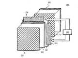
- FIG. 1is a perspective view schematically showing a configuration of a liquid crystal display device 1000 according to an embodiment of the present invention.
- the liquid crystal display device 1000includes a TFT substrate (semiconductor device) 100 and a counter substrate 200 that face each other with a liquid crystal layer interposed therebetween, and polarized light disposed on the outer sides of the TFT substrate 100 and the counter substrate 200. Plates 210 and 220 and a backlight unit 230 that emits display light toward the TFT substrate 100 are provided.
- a scanning line driving circuit 240 for driving a plurality of scanning lines (gate bus lines) and a signal line driving circuit 250 for driving a plurality of signal lines (data bus lines)are arranged on the TFT substrate 100.
- the scanning line driving circuit 240 and the signal line driving circuit 250are connected to a control circuit 260 disposed inside or outside the TFT substrate 100.
- a scanning signal for switching on / off of the TFTis supplied from the scanning line driving circuit 240 to the plurality of scanning lines, and the display signal (to the pixel electrode 20 shown in FIG. 3) is supplied from the signal line driving circuit 250. Applied voltage) is supplied to a plurality of signal lines.
- the counter substrate 200includes a color filter and a common electrode.
- the color filterincludes an R (red) filter, a G (green) filter, and a B (blue) filter, each of which is arranged corresponding to a pixel.
- the common electrodeis formed so as to cover the plurality of pixel electrodes 20 with the liquid crystal layer interposed therebetween. In accordance with the potential difference applied between the common electrode and each pixel electrode 20, the liquid crystal molecules between both electrodes are aligned for each pixel, and display is performed.
- FIG. 2is a plan view schematically showing the configuration of the TFT substrate 100
- FIG. 3is a plan view schematically showing the configuration of the display area DA of the TFT substrate 100.
- the TFT substrate 100has a display part DA and a peripheral part FA located outside the display part DA.
- electrical elementssuch as a scanning line driving circuit 240, a signal line driving circuit 250, and a voltage supply circuit are arranged in a COG (Chip on Glass) system. Electric elements such as TFTs and diodes in the peripheral portion FA can be formed in the same manufacturing process as the TFTs of the display portion DA.
- a terminal portion 30 for attaching an external elementsuch as FPC (Flexible Printed Circuits) is disposed near the outer end portion of the peripheral portion FA.
- a connection portion 25that electrically connects an upper wiring such as a signal line and a lower wiring such as a scanning line is formed in the peripheral portion FA.
- connection wiringsare formed at the boundary between the display area DA and the peripheral area FA.
- Each signal line 12is electrically connected to a connection wiring via a connection portion formed correspondingly.
- the signal line 12 that is the upper wiringis connected to the connection wiring that is the lower wiring by the connecting portion.
- a plurality of pixels 50are arranged in a matrix, and a plurality of scanning lines 14 and a plurality of signal lines 12 are arranged so as to be orthogonal to each other.
- a part of the scanning line 14constitutes a gate electrode of the TFT 10.
- TFTthin film transistor
- Each pixel 50is provided with a pixel electrode 20 made of, for example, ITO (Indium Tin Oxide), which is electrically connected to the drain electrode of the TFT 10.
- a storage capacitor line (also referred to as a Cs line) 16extends in parallel with the scanning line 14 between two adjacent scanning lines 14.
- An auxiliary capacitance (Cs) 18is formed in each pixel 10, and a part of the auxiliary capacitance line 16 serves as an auxiliary capacitance electrode (lower electrode) of the auxiliary capacitance 18.
- the auxiliary capacitance 18is configured by the auxiliary capacitance electrode, the auxiliary capacitance counter electrode (upper electrode), and a layer disposed between the two electrodes.
- the drain electrode of the TFT 10is connected to a storage capacitor counter electrode, and the storage capacitor counter electrode is connected to the pixel electrode 20 through a contact hole formed in the interlayer insulating layer.
- the gate electrode, the scanning line 14, the auxiliary capacitance line 16, and the auxiliary capacitance electrode of the TFT 10are formed of the same material and in the same process.
- the source electrode and drain electrode, the signal line 12, and the storage capacitor counter electrode of the TFT 10are formed of the same material and in the same process.
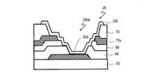
- FIG. 4is a cross-sectional view schematically showing the configuration of the TFT 10 on the TFT substrate 100 (also referred to as “semiconductor device 100”) according to the first embodiment.
- the TFT 10includes a gate electrode 62 formed on a substrate 60 such as a glass substrate, and an oxygen supply layer 64 formed on the substrate 60 so as to cover a part of the gate electrode 62.
- a gate insulating layer 66(also referred to simply as “insulating layer 66”) formed on the oxygen supply layer 64, an oxide semiconductor layer 68 formed on the gate insulating layer 66, and a gate insulating layer 66 and a source electrode 70s and a drain electrode 70d formed on the oxide semiconductor layer 68, and a protective layer 72 formed on the source electrode 70s and the drain electrode 70d.
- the pixel electrode 20 made of a transparent conductive materialis formed on the protective layer 72.
- a contact hole 74his formed in the protective layer 72 below the pixel electrode 20, and the pixel electrode 20 is in contact with the drain electrode 70d of the TFT 10 at the bottom of the contact hole 74h.
- the gate electrode 62may have a two-layer structure in which an upper gate electrode made of, for example, copper (Cu) is formed on a lower gate electrode made of, for example, titanium (Ti).
- the gate electrodemay have a three-layer structure such as Ti / Al (aluminum) / Ti.
- the oxygen supply layer 64is a layer made of a material containing water (H 2 O), an OR group, or an OH group.
- the oxygen supply layer 64is formed by applying a spin-on glass (SOG) material including, for example, a silicone resin by a spin coating method.
- SOGspin-on glass
- other materials including silanol (Si (OH) 4 ), alkoxysilane, siloxane resin, and the likecan be used.
- the oxygen supply layer 64may be formed of other resin materials containing silanol groups or Si—OH groups. Further, the oxygen supply layer 64 may be formed of an acrylic resin, an ester polymerization resin, or a resin material containing a CO—OR group.
- the gate insulating layer 66is made of silicon nitride.
- the gate insulating layer 66may be formed of silicon oxide or a two-layer structure of a silicon nitride layer and a silicon oxide layer.
- the gate insulating layer 66is in contact with the gate electrode 62 in the opening formed in the oxygen supply layer 64.
- the oxide semiconductor layer 68is a layer made of an In—Ga—Zn—O-based semiconductor (IGZO).
- the source electrode 70s and the drain electrode 70d formed on the oxide semiconductor layer 68are conductive layers having a three-layer structure of Ti / Al / Ti.
- the source electrode 70s and the drain electrode 70dmay have a two-layer structure such as Al / Ti, Cu / Ti, or Cu / Mo (molybdenum).
- the protective layer 72is made of silicon oxide (SiO 2 ) or silicon nitride (SiN x ). There may be a configuration in which the protective layer 72 is not provided.
- the oxygen supply layer 64contains H 2 O, an OR group, or an OH group
- a heat treatment stepsuch as annealing.
- H 2 O, OH group, or OR groupis diffused, and defects due to oxygen deficiency or the like in the oxide semiconductor layer 68 are compensated. Therefore, the characteristics of TFT can be improved, and a high-quality semiconductor device with little variation for each TFT can be provided.
- the oxide semiconductor layer 64has moved from the oxygen supply layer 64 to the gate insulating layer 66.
- the H 2 O, OR group, or OH groupis reflected on the bottom surfaces of the source electrode 70 s and the drain electrode 70 d, and part of the H 2 O, OR group, or OH group moves toward the oxide semiconductor layer 68.
- the source electrode 70s and the drain electrode 70dserve as a diffusion prevention layer, and thus more H 2 O, OR is added to the oxide semiconductor layer 68.
- a group or OH groupis supplied to repair more defects.
- FIG. 6Ais a graph showing the voltage-current characteristics of the TFT 10 of Embodiment 1
- FIG. 6Bis a graph showing the voltage-current characteristics of a TFT having no oxygen supply layer.
- the horizontal axisrepresents the gate voltage value
- the vertical axisrepresents the source-drain current value
- the characteristic when the drain voltage is 10Vis a solid line
- the characteristic when the drain voltage is 0.1V.are indicated by broken lines.
- the rising characteristic (S value) of the current in the vicinity of the gate voltage of 0 Vis constant regardless of the drain voltage, and the applied voltage from when the TFT is turned on. Appropriate current value according to is obtained.
- the S valuediffers for each drain voltage, and the rising position of the ON current and the OFF current value vary. From these comparisons, it can be seen that the TFT 10 having the oxygen supply layer 54 of Embodiment 1 can provide a high-performance semiconductor device with more stable TFT characteristics.
- FIGS. 7A to 7F and FIGS. 8G to 8Hare schematic cross-sectional views showing the manufacturing process of the TFT substrate 100.
- FIG. 7A to 7F and FIGS. 8G to 8Hare schematic cross-sectional views showing the manufacturing process of the TFT substrate 100.
- the thickness of the Ti layeris 30 to 150 nm
- the thickness of the Cu layeris 200 to 500 nm.
- the two stacked layersare patterned using a known photolithography method and wet etching method (first mask process) to obtain the gate electrode 62 shown in FIG.
- the scanning line 14, the auxiliary capacitance line 16, the auxiliary capacitance electrode, the lower wiring, and the likeare also formed at the same time. Thereafter, the remaining resist is stripped and the substrate is cleaned.
- a silicone resin or SOG materialis used for the oxygen supply material 64m.
- SOG materialother materials including silanol (for example, Si (OH) 4 ), alkoxysilane, siloxane resin, and the like can be used.
- the oxygen supply layer 64may be formed of other resin materials containing silanol groups or Si—OH groups. Further, the oxygen supply layer 64 may be formed of an acrylic resin, an ester polymerization resin, or a resin material containing a CO—OR group.
- the gate insulating layer 66is a silicon nitride layer stacked to a thickness of 100 to 700 nm by plasma CVD. Instead of silicon nitride, silicon oxide (SiO 2 ) may be stacked, or both silicon nitride and silicon oxide may be stacked.
- the gate insulating layer 66is in contact with the gate electrode 62 in the opening of the oxygen supply layer 64.
- the oxide semiconductoris formed by stacking, for example, an In—Ga—Zn—O-based semiconductor (IGZO) with a thickness of 10 to 100 nm by a sputtering method.
- An oxide semiconductormay be stacked by a coating method or an inkjet method.
- the stacked oxide semiconductoris patterned by a photolithography method, for example, a wet etching method using oxalic acid (third mask process), and an oxide that becomes a channel layer of the TFT 10 as shown in FIG. A physical semiconductor layer 68 is obtained. Thereafter, the remaining resist is stripped and the substrate is cleaned.
- a photolithography methodfor example, a wet etching method using oxalic acid (third mask process)
- oxalic acidthird mask process
- the remaining resistis stripped and the substrate is cleaned.
- the oxide semiconductoranother type of oxide semiconductor film may be used instead of IGZO.
- silicon oxideis laminated on the entire substrate by a CVD method.
- silicon nitridemay be stacked, or both silicon oxide and silicon nitride may be stacked.
- the layer thus formedis called a PAS film.
- the PAS filmwas annealed at a temperature of 200 ° C. to 400 ° C. in an air atmosphere. During the annealing process, a reflective layer is formed between the lower surfaces of the source electrode 70 s and the drain electrode 70 d and the oxide semiconductor layer 68.
- the low reflection layeran oxidation-reduction reaction occurs between titanium constituting the lower layer of the source electrode 70s and the drain electrode 70d and the oxide semiconductor layer 68, and at the same time titanium is oxidized, indium in the oxide semiconductor 68 is obtained. Is formed by reduction.
- external lightsuch as sunlight or sunlight incident on the TFT substrate 10 is repeatedly reflected between the lower surface of the source electrode 70s and the drain electrode 70d and the upper surface of the gate electrode 62, Most of them reach the channel portion of the oxide semiconductor layer 68 and deteriorate the TFT characteristics.
- the TFT 10 of the present embodimentsince the low reflection layer is formed as described above, reflection of incident light is prevented, and the amount of light incident on the channel portion can be reduced. Thereby, it is possible to provide a highly reliable TFT substrate in which variation in characteristics is suppressed.
- the laminated PAS filmis patterned by a photolithography method (fifth mask process) to obtain a protective layer 72 shown in FIG.
- An opening 72his formed in the protective layer 72 by patterning.
- the TFT substrate 100 having the TFT 10is completed.
- connection portion 25 in the TFT substrate 100will be described with reference to FIGS. 9 to 11 schematically show cross sections of first to third configuration examples of the connecting portion 25, respectively.
- the connection portion 25includes a lower wiring 62 d formed on the substrate 60, an oxygen supply layer 64 formed on the lower wiring 62 d, and an oxygen supply layer 64.
- a gate insulating layer 66 formed above and an upper wiring 70 u formed on the gate insulating layer 66are provided.
- the lower wiring 62dis a metal layer formed of the same material as the gate electrode 62.
- the upper wiring 70uis a metal layer formed of the same material simultaneously with the source electrode 70s and the drain electrode 70d.
- each of the oxygen supply layer 64 and the gate insulating layer 66is provided with an opening at a position overlapping each other, and a contact hole 25ha is formed so as to penetrate these two layers.
- the opening of the gate insulating layer 66is larger than the opening of the oxygen supply layer 64, and the side surfaces of the gate insulating layer 66 and the oxygen supply layer 64 are formed stepwise in the contact hole 25ha.
- the upper wiring 70u and the lower wiring 62dare connected through a contact hole 25ha. That is, the upper wiring 70u formed in the contact hole 25ha is connected to the lower wiring 62d at the bottom of the contact hole 25ha.
- the metal layer of the upper wiring 70uWhen laminating the metal layer of the upper wiring 70u, if the side surface of the contact hole 25ha is a steep slope, the metal layer is likely to be cut at the side surface, and there is a risk of disconnection at the connection portion.
- the upper wiring 70uis formed not on the steeply inclined side surface but on the stepped side surfaces of the gate insulating layer 66 and the oxygen supply layer 64, and thus the upper wiring 70u is hardly cut. Therefore, the highly reliable connection part 25 can be formed.
- the connecting portion 25includes a lower wiring 62d formed on the substrate 60, an oxygen supply layer 64 formed on the lower wiring 62d, and an oxygen supply layer 64.
- the gate insulating layer 66formed thereon, the upper wiring 70u formed on the gate insulating layer 66, the protective layer 72 formed on the upper wiring 70u, and the conductive formed on the protective layer 72 Layer 20t.
- the lower wiring 62dis a metal layer formed of the same material simultaneously with the gate electrode 62
- the upper wiring 70uis a metal layer formed of the same material simultaneously with the source electrode 70s and the drain electrode 70d.
- the conductive layer 20tis formed of the same material as the pixel electrode 20 at the same time.
- each of the oxygen supply layer 64, the gate insulating layer 66, the upper wiring 70u, and the protective layer 72is provided with an opening at an overlapping position.
- the openingis formed so as to increase from the lower layer to the upper layer, and a contact hole 25hb is formed so as to penetrate these layers.
- the end portion of each layeris formed in a stepped shape so as to be positioned on the outer side as it becomes higher.
- the upper wiring 70u and the lower wiring 62dare connected via the conductive layer 20t in the contact hole 25hb. That is, in the contact hole 25hb, the conductive layer 20t is formed so as to cover the side surfaces of the oxygen supply layer 64, the gate insulating layer 66, the upper wiring 70u, and the protective layer 72. Wiring 70u is connected, and conductive layer 20t and lower wiring 62d are connected at the bottom of contact hole 25ha.
- a metalsuch as ITO or IZO is laminated by sputtering. If the side surface of the contact hole 25ha is a steep slope, the metal layer is cut or the metal layer and the upper wiring 70u are formed. Contact failure is likely to occur. Also, if the end of each layer is to be formed at the same position, the lower layer end is formed outside the upper layer end due to mask misalignment, variation in etching shift, overhang, etc. in photolithography. Can occur. This causes disconnection in the conductive layer 20t.
- the side surface of each layeris formed so as to be positioned on the outer side as it becomes higher, so the side surface of the contact hole 25hb is formed in a staircase shape, the disconnection of the conductive layer 20t and the upper side of the conductive layer 20t. Contact failure with the wiring 70u is prevented.
- the connection in the multi-layer structure portionis performed through one contact hole, the area of the connection portion can be reduced. As a result, the density and size of the TFT substrate can be reduced.
- the contact hole 25hbcan be formed by collectively etching each layer using halftone exposure, resist ashing, or the like. In this case, the manufacturing efficiency is improved, and the TFT substrate can be manufactured at a low cost.
- the connection portion 25 according to the third configuration exampleincludes a lower wiring 62d formed on the substrate 60, an oxygen supply layer 64 formed on the lower wiring 62d, and an oxygen supply layer 64.
- the lower wiring 62dis a metal layer formed of the same material simultaneously with the gate electrode 62
- the upper wiring 70uis a metal layer formed of the same material simultaneously with the source electrode 70s and the drain electrode 70d.
- the conductive layer 20tis formed of the same material as the pixel electrode 20 at the same time.
- a first contact hole 25hc that penetrates the protective layer 72 and a second contact hole 25hd that penetrates the protective layer 72, the gate insulating layer 66, and the oxygen supply layer 64are formed.
- the upper wiring 70u and the conductive layer 20tare connected in the first contact hole 25hc. That is, the conductive layer 20t is formed in the contact hole 25hc so as to cover the side surface of the protective layer 72, and the conductive layer 20t and the upper wiring 70u are connected at the bottom of the contact hole 25hc.
- the conductive layer 20t and the lower wiring 62dare connected in the second contact hole 25hd.
- the conductive layer 20tis formed in the contact hole 25hd so as to cover the side surfaces of the protective layer 72, the gate insulating layer 66, and the oxygen supply layer 64, and the conductive layer 20t and the lower wiring are formed at the bottom of the contact hole 25hd. 62d is connected.
- the upper wiring 70u and the lower wiring 62dare electrically connected via the conductive layer 20t.
- the side surfaces of the contact holes 25hc and 25hdmay be formed in a step shape, thereby preventing disconnection of the conductive layer 20t.
- FIG. 12is a cross-sectional view schematically showing the configuration of the TFT 10 according to the second embodiment.
- the basic configuration of the TFT substrate according to the present embodimentis the same as that of the TFT substrate 100 of Embodiment 1 except as described below.
- the TFT 10includes a gate electrode 62, an oxygen supply layer 64, a gate insulating layer 66, an oxide semiconductor layer 68, a source electrode 70s, and a drain electrode that are sequentially stacked on the substrate 60, as in the first embodiment. 70d and a protective layer 72 are provided. Further, the TFT 10 of this embodiment includes a second oxygen supply layer 78 formed on the protective layer 72. A form in which the protective layer 72 is not formed is also included in the TFT 10 of this embodiment. The second oxygen supply layer 78 is formed instead of the interlayer insulating layer 74 in the first embodiment. An interlayer insulating layer 74 may be formed on the second oxygen supply layer 78.
- the second oxygen supply layer 78is formed by applying an acrylic resin by, for example, a spin coating method in the step (H) of the first embodiment.
- An SOG material containing silicone resin or the likemay be applied instead of the acrylic resin.
- the second oxygen supply layer 78is a layer made of a material containing H 2 O, an OR group, or an OH group, and can be formed of the material for the oxygen supply layer 64 described in the first embodiment. .
- H 2 O, OR groups, or OH groupscan be supplied not only from the oxygen supply layer 64 but also from the second oxygen supply layer 78 to the channel portion of the oxide semiconductor layer 68. . Therefore, the oxide semiconductor layer 68 in which defects are further repaired than in Embodiment 1 can be obtained, and a highly reliable semiconductor device with more excellent TFT characteristics can be obtained.
- FIG. 13is a cross-sectional view schematically showing the configuration of the TFT substrate 100 according to the third embodiment.
- the basic configuration of the TFT substrate 100 according to the present embodimentis the same as that of the TFT substrate 100 of Embodiment 1 except as described below, and can be used as the TFT substrate 100 shown in FIGS.
- the TFT substrate 100has a contact portion 85, a wiring cross portion 87, a TFT portion 80, and a Cs portion 88.
- the connection portion 25is formed in the contact portion 85
- the TFT 10is formed in the TFT portion 80
- the auxiliary capacitor 18is formed in the Cs portion 88.
- the wiring cross portion 87is a portion where the signal line 12 as the upper layer wiring and the scanning line 14 as the lower layer wiring intersect.
- connection portion 25 in the contact portion 85is basically the same as the connection portion 25 of the second configuration example of the first embodiment.
- a second oxygen supply layer 78is laminated instead of the interlayer insulating layer 74 in the second configuration example.
- the side surfaces of the contact hole 25hbare formed on the side surface of the contact hole 25hb so as to be positioned on the outer side as the upper layer becomes higher. The disconnection of the layer 20t and the contact failure between the conductive layer 20t and the upper wiring 70u are prevented.
- the wiring connectionis performed through one contact hole, the area of the connection portion can be reduced.
- the connection portion 25 of the first and third configuration examples of the first embodimentmay be formed in the contact portion 85.
- the wiring cross portion 87includes a substrate 60, the scanning line 14 formed on the substrate 60, an oxygen supply layer 64 laminated to cover the scanning line, and a gate insulating layer formed on the oxygen supply layer 64. 66, a signal line 12 formed on the gate insulating layer 66, a protective layer 72 formed to cover the signal line 12, and a second oxygen supply layer 78 formed on the protective layer. Yes.
- the TFT 10 of Embodiment 2is formed.
- the drain electrode 70 d of the TFT 10 and the pixel electrode 20are connected via a contact hole formed in the protective layer 72 and the second oxygen supply layer 78.
- an auxiliary capacitance electrode 62c, an oxygen supply layer 64, a gate insulating layer 66, an auxiliary capacitance counter electrode 70c, a protective layer 72, and a second oxygen supply layer 78are stacked in this order.
- the auxiliary capacitance 18is configured by the auxiliary capacitance electrode 62c, the auxiliary capacitance counter electrode 70c facing the auxiliary capacitance electrode 62c, and the gate insulating layer 66 sandwiched between the two electrodes.
- An opening of the oxygen supply layer 64is formed between the electrodes, and a gate insulating layer 66 is formed so as to fill the opening.
- the distance between the two electrodescan be reduced, so that the auxiliary capacitor 18 having a large capacity can be formed in a narrow region even in the TFT substrate 100 having a multilayer structure including the oxygen supply layer 64.
- FIG. 14is a cross-sectional view schematically showing the configuration of the TFT 10 according to the fourth embodiment.
- the basic configuration of the TFT substrate according to the present embodimentis the same as that of the TFT substrate 100 of Embodiment 1 except as described below.
- the TFT 10includes a gate electrode 62 formed on the substrate 60, a gate insulating layer 66 laminated so as to cover the gate electrode 62, and an oxygen formed on the gate insulating layer 66.
- a protective layer 72is provided.
- the oxygen supply layer 64is disposed between the gate insulating layer 66 and the oxide semiconductor layer 68.
- the oxygen supply layer 64has an opening on the gate insulating layer 66 above the gate electrode 62, and the oxide semiconductor layer 64 is in contact with the gate insulating layer 66 in the opening.
- the portion of the oxide semiconductor layer 64 in contact with the gate insulating layer 66is a portion corresponding to the channel portion CH of the TFT 10.
- the other part of the oxide semiconductor layer 64is in direct contact with the oxygen supply layer 64.
- the gate insulating layer 66is laminated on the substrate 60 by the CVD method so as to cover the gate electrode 62.
- an oxygen supply materialis applied onto the gate insulating layer 66 by a spin coat method or the like. The same material as that described in Embodiment 1 is used for the oxygen supply material 64m.
- step (C)the oxygen supply material is patterned by photolithography (second mask step), and the oxygen supply layer 64 is completed. At the time of patterning, an opening is provided above the gate electrode 62.
- the oxide semiconductor layer 68since the oxide semiconductor layer 68 has a portion in direct contact with the oxygen supply layer 64, oxygen is supplied from the oxygen supply layer 64 to the oxide semiconductor layer 68 with high efficiency. Therefore, it is possible to provide a high-performance TFT in which defects are further repaired.
- the oxygen supply layer 64is in direct contact with the channel portion CH of the oxide semiconductor layer 68, since there are many impurities in the oxygen supply layer 64, there is a concern that the reliability of the TFT may be reduced due to diffusion of the impurities. is there. Therefore, it is preferable to dispose a layer made of a material with few impurities, such as a silicon oxide film, at a portion in contact with the channel portion CH.
- the oxide semiconductor layer 68 of the channel portion CHis not in direct contact with the oxygen supply layer 64 but is in contact with the gate insulating layer 66 made of a silicon oxide film or the like, so that the reliability of the TFT is further improved. Can do.
- a gate insulating layer 66 made of silicon oxide, silicon nitride, or the likeis formed on the opposite side of the oxygen supply layer 64 from the oxide semiconductor layer 68.
- the gate insulating layer 66 made of such a materialhas a function of limiting diffusion of H 2 O or the like. Therefore, more H 2 O, OR groups, or OH groups can be moved from the oxygen supply layer 64 to the oxide semiconductor layer 68, whereby the oxide semiconductor layer 68 with more repaired defects can be obtained.
- FIG. 15is a cross-sectional view schematically showing a configuration of an organic EL display device 1002 (also simply referred to as “display device 1002”).
- the display device 1002includes a TFT substrate 140, a hole transport layer 144 provided on the TFT substrate 140, a light emitting layer 146 provided on the hole transport layer 144, and a light emitting layer 146.
- a counter electrode 148 provided aboveis provided.
- the hole transport layer 144 and the light emitting layer 146constitute an organic EL layer.
- the organic EL layeris divided by insulating protrusions 147, and the divided organic EL layer becomes an organic EL layer of one pixel.
- the TFT substrate 140has basically the same configuration as the TFT substrate 100 of the first to fourth embodiments, and includes the TFT 10 formed on the substrate 60.
- the TFT 10 described in Embodiments 1 to 4can be used as the TFT 10.
- the TFT substrate 140has an interlayer insulating layer 74 and a pixel electrode 109 formed on the interlayer insulating layer 74 so as to cover the TFT 10.
- the pixel electrode 109is connected to the drain electrode of the TFT 10 in a contact hole formed in the interlayer insulating layer 74. Since the planar configuration of the TFT substrate 140 is basically the same as that shown in FIGS. 2 and 3, the description thereof is omitted. Note that the TFT substrate 140 may have a form having no auxiliary capacitance.
- Known materials and structuresmay be used for the materials of the hole transport layer 144, the light emitting layer 146, and the counter electrode 148, and the layer structure thereof.
- a hole injection layermay be provided between the hole transport layer 144 and the light emitting layer 146 in order to increase the hole injection efficiency.
- the organic EL display device 1002 of this embodimentuses the TFT 10 described in the first to fourth embodiments, the same effects as those described in the first to fourth embodiments can be obtained. According to this embodiment, it is possible to provide the organic EL display device 1002 capable of performing high-performance display with high manufacturing efficiency.
- the present inventionis suitably used for a semiconductor device having a thin film transistor, and a display device such as a liquid crystal display device or an organic EL display device having the thin film transistor on a TFT substrate.
Landscapes
- Engineering & Computer Science (AREA)
- Physics & Mathematics (AREA)
- Microelectronics & Electronic Packaging (AREA)
- General Physics & Mathematics (AREA)
- Condensed Matter Physics & Semiconductors (AREA)
- Manufacturing & Machinery (AREA)
- Computer Hardware Design (AREA)
- Power Engineering (AREA)
- Nonlinear Science (AREA)
- Mathematical Physics (AREA)
- Crystallography & Structural Chemistry (AREA)
- Chemical & Material Sciences (AREA)
- Optics & Photonics (AREA)
- Geometry (AREA)
- Thin Film Transistor (AREA)
- Liquid Crystal (AREA)
- Electroluminescent Light Sources (AREA)
Abstract
Description
Translated fromJapanese本発明は、薄膜トランジスタを備える半導体装置および表示装置に関する。The present invention relates to a semiconductor device including a thin film transistor and a display device.
アクティブマトリクス型の液晶表示装置や有機EL(Electro Luminescence)表示装置は、一般に、画素毎にスイッチング素子として薄膜トランジスタ(Thin Film Transistor;以下、「TFT」とも呼ぶ)が形成された基板(以下、「TFT基板」と呼ぶ)と、対向電極およびカラーフィルタなどが形成された対向基板と、TFT基板と対向基板との間に設けられた液晶層などの光変調層とを備えている。In general, an active matrix liquid crystal display device or an organic EL (Electro Luminescence) display device is a substrate (hereinafter referred to as “TFT”) in which a thin film transistor (hereinafter also referred to as “TFT”) is formed as a switching element for each pixel. A counter substrate on which a counter electrode and a color filter are formed, and a light modulation layer such as a liquid crystal layer provided between the TFT substrate and the counter substrate.
TFT基板には、複数のソース配線と、複数のゲート配線と、これらの交差部にそれぞれ配置された複数のTFTと、液晶層などの光変調層に電圧を印加するための画素電極と、補助容量配線および補助容量電極などが形成されている。The TFT substrate includes a plurality of source wirings, a plurality of gate wirings, a plurality of TFTs disposed at intersections thereof, a pixel electrode for applying a voltage to a light modulation layer such as a liquid crystal layer, and an auxiliary Capacitance wiring, auxiliary capacitance electrodes, and the like are formed.
TFT基板の構成は、例えば特許文献1に開示されている。以下、図面を参照しながら、特許文献1に開示されたTFT基板の構成を説明する。The configuration of the TFT substrate is disclosed in Patent Document 1, for example. Hereinafter, the configuration of the TFT substrate disclosed in Patent Document 1 will be described with reference to the drawings.
図16(a)は、TFT基板の概略を示す模式的な平面図であり、図16(b)は、TFT基板における1個の画素を示す拡大平面図である。また、図17は、図16に示す半導体装置におけるTFTおよび端子部の断面図である。FIG. 16A is a schematic plan view showing an outline of the TFT substrate, and FIG. 16B is an enlarged plan view showing one pixel on the TFT substrate. FIG. 17 is a cross-sectional view of the TFT and the terminal portion in the semiconductor device shown in FIG.
図16(a)に示すように、TFT基板は、複数のゲート配線2016と、複数のソース配線2017とを有している。これらの配線2016、2017で包囲されたそれぞれの領域2021が「画素」となる。TFT基板のうち画素が形成される領域(表示領域)以外の領域2040には、複数のゲート配線2016およびソース配線2017のそれぞれを駆動回路に接続するための複数の接続部2041が配置されている。各接続部2041は、外部配線と接続するための端子部を構成する。As shown in FIG. 16A, the TFT substrate has a plurality of
図16(b)および図17に示すように、画素となる各領域2021を覆うように画素電極2020が設けられている。また、各領域2021にはTFTが形成されている。TFTは、ゲート電極Gと、ゲート電極Gを覆うゲート絶縁膜2025、2026と、ゲート絶縁膜2026上に配置された半導体層2019と、半導体層2019の両端部にそれぞれ接続されたソース電極Sおよびドレイン電極Dとを有している。TFTは保護膜2028で覆われている。保護膜2028と画素電極2020との間には、層間絶縁膜2029が形成されている。TFTのソース電極Sはソース配線2017に、ゲート電極Gはゲート配線2016に接続されている。また、ドレイン電極Dは、コンタクトホール2030内で画素電極2020に接続されている。As shown in FIGS. 16B and 17, a
また、ゲート配線2016と平行に補助容量配線2018が形成されている。補助容量配線2018は補助容量に接続されている。ここでは、補助容量は、ドレイン電極Dと同じ導電膜から形成された補助容量電極2018bと、ゲート配線2016と同じ導電膜から形成された補助容量電極2018aと、それらの間に位置するゲート絶縁膜2026とから構成されている。Further, an
各ゲート配線2016またはソース配線2017から延びた接続部2041上には、ゲート絶縁膜2025、2026および保護膜2028が形成されておらず、接続部2041の上面と接するように接続配線2044が形成されている。これにより、接続部2041と接続配線2044との電気的な接続が確保されている。The
なお、図17に示すように、液晶表示装置では、TFT基板は、液晶層2015を挟んで、対向電極やカラーフィルタが形成された基板2014と対向するように配置される。As shown in FIG. 17, in the liquid crystal display device, the TFT substrate is disposed so as to face the
このようなTFT基板を製造する際には、画素となる領域2021(「画素部」ともいう。)と、端子部とを共通のプロセスで形成し、マスク数や工程数の増大を抑えることが好ましい。When manufacturing such a TFT substrate, a region 2021 (also referred to as a “pixel portion”) that serves as a pixel and a terminal portion are formed by a common process to suppress an increase in the number of masks and processes. preferable.
上記のTFT基板を製造しようとすると、ゲート絶縁膜2025、2026および保護膜2028のうち端子配置領域2040に位置する部分、および、ゲート絶縁膜2025および保護膜2028のうち補助容量が形成される領域に位置する部分をエッチングする必要がある。特許文献1には、有機絶縁膜を用いて層間絶縁膜2029を形成し、これをマスクとして、これらの絶縁膜2025、2026、および保護膜2028をエッチングすることが開示されている。When the above TFT substrate is manufactured, a portion of the
近年、シリコン半導体膜の代わりに、IGZO(InGaZnOX)などの酸化物半導体膜を用いてTFTのチャネル層を形成することが提案されている。このようなTFTを「酸化物半導体TFT」と称する。酸化物半導体がアモルファスシリコンよりも高い移動度を有していることから、酸化物半導体TFTは、アモルファスシリコンTFTよりも高速で動作することが可能である。また、酸化物半導体膜は、多結晶シリコン膜よりも簡便なプロセスで形成されるため、大面積が必要とされる装置にも適用できる。In recent years, it has been proposed to form a TFT channel layer using an oxide semiconductor film such as IGZO (InGaZnOx ) instead of a silicon semiconductor film. Such a TFT is referred to as an “oxide semiconductor TFT”. Since an oxide semiconductor has higher mobility than amorphous silicon, an oxide semiconductor TFT can operate at a higher speed than an amorphous silicon TFT. In addition, since the oxide semiconductor film is formed by a simpler process than the polycrystalline silicon film, the oxide semiconductor film can be applied to a device that requires a large area.
特許文献2には、酸化物半導体TFTの一例が記載されている。また、特許文献3には、非晶質酸化物半導体の活性層を備えた電界効果型トランジスタの例が記載されている。
特許文献3には、非晶質酸化物半導体層を形成するために、基板上に非晶質酸化物半導体層を形成する前に、基板表面にオゾン雰囲気中で紫外線を照射したり、基板表面にプラズマを照射したり、あるいは基板表面を過酸化水素で洗浄することが記載されている。また、この文献には、非晶質酸化物を含む活性層を形成する工程を、オゾンガス、窒素酸化物ガス等の雰囲気の中で行なうことや、基板上に非晶質酸化物を形成した後に、非晶質酸化物の成膜温度よりも高い温度で熱処理を行なうことなどが記載されている。In Patent Document 3, in order to form an amorphous oxide semiconductor layer, before the amorphous oxide semiconductor layer is formed on the substrate, the substrate surface is irradiated with ultraviolet rays in an ozone atmosphere, Describes that plasma is irradiated or that the surface of the substrate is washed with hydrogen peroxide. Further, in this document, the step of forming an active layer containing an amorphous oxide is performed in an atmosphere such as ozone gas or nitrogen oxide gas, or after an amorphous oxide is formed on a substrate. Further, it is described that the heat treatment is performed at a temperature higher than the film formation temperature of the amorphous oxide.
しかしながら、酸化物半導体TFTでは、TFTの製造プロセス中、例えば熱処理工程等において酸素欠損が生じ、キャリア電子が生じて不要なOFF電流が発生するなどの問題が発生し得る。また、ソース・ドレイン電極のエッチング工程やその上部の絶縁層の形成工程において、下方にある酸化物半導体膜が、還元作用等のダメージを受けるという問題も生じ得る。However, in the oxide semiconductor TFT, problems such as generation of oxygen vacancies during the TFT manufacturing process, for example, a heat treatment step, and generation of carrier electrons to generate unnecessary OFF current may occur. In addition, in the etching process of the source / drain electrodes and the formation process of the insulating layer thereabove, there may be a problem that the underlying oxide semiconductor film is damaged by a reducing action or the like.
本願発明者が検討した結果、酸化物半導体層がその下部のゲート絶縁層、またはその上部の保護層等と接する構成の酸化物半導体TFTにおいては、酸化物半導体層内部、または酸化物半導体層と絶縁層、保護層等との界面近傍に酸素欠損等による欠陥準位が発生し易く、それにより、TFTの特性低下、信頼性低下、品質のばらつき増加等の問題が発生することがわかった。As a result of examination by the inventors of the present application, in an oxide semiconductor TFT having a configuration in which the oxide semiconductor layer is in contact with the gate insulating layer below or the protective layer above the oxide semiconductor layer, the inside of the oxide semiconductor layer or the oxide semiconductor layer It has been found that defect levels due to oxygen vacancies are likely to occur near the interface with the insulating layer, protective layer, etc., thereby causing problems such as degradation of TFT characteristics, reliability, and increased quality variation.
上記特許文献3には、特性の優れたトランジスタを得るために、非晶質酸化物を形成した後に、非晶質酸化物の成膜温度よりも高い温度で熱処理を行なうことなどが記載されているが、このような方法によっても、酸素欠損に起因する欠陥準位の低減を行なうことはできず、良好なTFT特性を得ることは難しい。Patent Document 3 describes that after an amorphous oxide is formed, heat treatment is performed at a temperature higher than the film formation temperature of the amorphous oxide in order to obtain a transistor having excellent characteristics. However, even with such a method, the defect level due to oxygen deficiency cannot be reduced, and it is difficult to obtain good TFT characteristics.
本発明は、上記に鑑みてなされたものであり、酸化物半導体TFTの酸化物半導体層に発生する欠陥を低減して、TFT特性の優れた半導体装置を製造することを目的とする。また本発明は、そのような半導体装置をTFT基板として備えた高性能の表示装置を提供することを目的とする。The present invention has been made in view of the above, and an object thereof is to manufacture a semiconductor device having excellent TFT characteristics by reducing defects generated in an oxide semiconductor layer of an oxide semiconductor TFT. It is another object of the present invention to provide a high-performance display device including such a semiconductor device as a TFT substrate.
本発明による半導体装置は、薄膜トランジスタを備えた半導体装置であって、基板上に形成された前記薄膜トランジスタのゲート電極および酸素供給層と、前記ゲート電極および前記酸素供給層の上に形成されたゲート絶縁層と、前記ゲート絶縁層の上に形成された前記薄膜トランジスタの酸化物半導体層と、前記ゲート絶縁層および前記酸化物半導体層の上に配置された、前記薄膜トランジスタのソース電極およびドレイン電極と、を備えている。A semiconductor device according to the present invention includes a thin film transistor, and includes a gate electrode and an oxygen supply layer of the thin film transistor formed on a substrate, and a gate insulation formed on the gate electrode and the oxygen supply layer. A thin film transistor, an oxide semiconductor layer of the thin film transistor formed on the gate insulating layer, and a source electrode and a drain electrode of the thin film transistor disposed on the gate insulating layer and the oxide semiconductor layer. I have.
ある実施形態では、前記酸素供給層が、水(H2O)、OR基、またはOH基を含む材料からなる層である。In one embodiment, the oxygen supply layer is a layer made of a material containing water (H2 O), an OR group, or an OH group.
ある実施形態では、前記酸素供給層が、シリコーン(silicone)樹脂、あるいはシラノール基またはSi-OH基を含む樹脂材料からなる。In one embodiment, the oxygen supply layer is made of a silicone resin, or a resin material containing silanol groups or Si—OH groups.
ある実施形態では、前記酸素供給層が、エステル重合樹脂、またはCO-OR基を含む樹脂材料からなる。In one embodiment, the oxygen supply layer is made of an ester polymerization resin or a resin material containing a CO-OR group.
ある実施形態では、前記酸素供給層が、アクリル樹脂またはSOG材料を含む材料からなる。In one embodiment, the oxygen supply layer is made of a material containing an acrylic resin or an SOG material.
ある実施形態では、半導体装置が、前記ゲート電極と同じ材料で形成された下部配線と、前記ソース電極および前記ドレイン電極と同じ材料で形成された上部配線と、前記上部配線と前記下部配線とが接続された接続部と、を備え、前記接続部において、前記上部配線と前記下部配線とが、前記酸素供給層および前記ゲート絶縁層を貫通するコンタクトホールを介して接続されている。In one embodiment, the semiconductor device includes a lower wiring formed of the same material as the gate electrode, an upper wiring formed of the same material as the source electrode and the drain electrode, and the upper wiring and the lower wiring. A connecting portion connected, wherein the upper wiring and the lower wiring are connected via a contact hole penetrating the oxygen supply layer and the gate insulating layer.
ある実施形態では、半導体装置が、前記ゲート電極と同じ材料で形成された下部配線と、前記ソース電極および前記ドレイン電極と同じ材料で形成された上部配線と、前記ソース電極および前記ドレイン電極の上に形成された保護層と、前記保護層の上に形成された導電層と、前記上部配線と前記下部配線とが接続された接続部と、を備え、前記接続部において、前記上部配線と前記下部配線とが、前記酸素供給層、前記ゲート絶縁層、および前記保護層を貫通するコンタクトホール内に形成された前記導電層を介して接続されている。In one embodiment, the semiconductor device includes a lower wiring formed of the same material as the gate electrode, an upper wiring formed of the same material as the source electrode and the drain electrode, and an upper surface of the source electrode and the drain electrode. A protective layer formed on the protective layer, a conductive layer formed on the protective layer, and a connection portion to which the upper wiring and the lower wiring are connected. In the connection portion, the upper wiring and the A lower wiring is connected to the oxygen supply layer, the gate insulating layer, and the conductive layer formed in a contact hole that penetrates the protective layer.
ある実施形態では、半導体装置が、前記ゲート電極と同じ材料で形成された下部配線と、前記ソース電極および前記ドレイン電極と同じ材料で形成された上部配線と、前記ソース電極および前記ドレイン電極の上に形成された保護層と、前記保護層の上に形成された導電層と、前記上部配線と前記下部配線とが接続された接続部と、を備え、前記接続部において、前記上部配線と前記導電層とが、前記保護層を貫通する第1コンタクトホールを介して接続されており、前記導電層と前記下部配線とが、前記保護層、前記ゲート絶縁層、および前記酸素供給層を貫通する第2コンタクトホールを介して接続されている。In one embodiment, the semiconductor device includes a lower wiring formed of the same material as the gate electrode, an upper wiring formed of the same material as the source electrode and the drain electrode, and an upper surface of the source electrode and the drain electrode. A protective layer formed on the protective layer, a conductive layer formed on the protective layer, and a connection portion to which the upper wiring and the lower wiring are connected. In the connection portion, the upper wiring and the A conductive layer is connected via a first contact hole that penetrates the protective layer, and the conductive layer and the lower wiring penetrate the protective layer, the gate insulating layer, and the oxygen supply layer. They are connected via the second contact hole.
ある実施形態では、半導体装置が、前記ゲート電極と同じ材料で形成された補助容量電極と、前記補助容量電極に対向するように、前記ソース電極および前記ドレイン電極と同じ材料で形成された補助容量対向電極と、を含む補助容量を備えている。In one embodiment, the semiconductor device has an auxiliary capacitance electrode formed of the same material as the gate electrode, and an auxiliary capacitance formed of the same material as the source electrode and the drain electrode so as to face the auxiliary capacitance electrode. And an auxiliary capacitor including a counter electrode.
ある実施形態では、半導体装置が、前記酸化物半導体層、前記ソース電極、および前記ドレイン電極の上部に形成された第2酸素供給層を備えている。In one embodiment, a semiconductor device includes a second oxygen supply layer formed on the oxide semiconductor layer, the source electrode, and the drain electrode.
ある実施形態では、半導体装置が、前記酸化物半導体層、前記ソース電極、および前記ドレイン電極と前記第2酸素供給層との間に形成された保護層を備えている。In one embodiment, a semiconductor device includes the oxide semiconductor layer, the source electrode, and a protective layer formed between the drain electrode and the second oxygen supply layer.
ある実施形態では、前記第2酸素供給層が、水(H2O)、OR基、またはOH基を含む材料からなる層である。In one embodiment, the second oxygen supply layer is a layer made of a material containing water (H2 O), an OR group, or an OH group.
本発明による他の半導体装置は、薄膜トランジスタを備えた半導体装置であって、基板上に形成された前記薄膜トランジスタのゲート電極と、前記ゲート電極の上に形成されたゲート絶縁層と、前記ゲート絶縁層の上に形成された酸素供給層と、前記酸素供給層の上に形成された前記薄膜トランジスタの酸化物半導体層と、前記酸化物半導体層の上に配置された、前記薄膜トランジスタのソース電極およびドレイン電極と、を備えている。Another semiconductor device according to the present invention is a semiconductor device including a thin film transistor, the gate electrode of the thin film transistor formed on a substrate, a gate insulating layer formed on the gate electrode, and the gate insulating layer An oxygen supply layer formed on the oxide supply layer; an oxide semiconductor layer of the thin film transistor formed on the oxygen supply layer; and a source electrode and a drain electrode of the thin film transistor disposed on the oxide semiconductor layer And.
ある実施形態では、前記酸素供給層に開口が形成されており、前記酸化物半導体層が、前記酸素供給層の前記開口の中で前記ゲート絶縁層と接している。In one embodiment, an opening is formed in the oxygen supply layer, and the oxide semiconductor layer is in contact with the gate insulating layer in the opening of the oxygen supply layer.
ある実施形態では、前記酸素供給層が、水(H2O)、OR基、またはOH基を含む材料からなる層である。In one embodiment, the oxygen supply layer is a layer made of a material containing water (H2 O), an OR group, or an OH group.
ある実施形態では、前記酸素供給層が、シリコーン樹脂、あるいはシラノール基またはSi-OH基を含む樹脂材料からなる。In one embodiment, the oxygen supply layer is made of a silicone resin, or a resin material containing silanol groups or Si—OH groups.
ある実施形態では、前記酸素供給層が、エステル重合樹脂、またはCO-OR基を含む樹脂材料からなる。In one embodiment, the oxygen supply layer is made of an ester polymerization resin or a resin material containing a CO-OR group.
ある実施形態では、前記酸素供給層が、アクリル樹脂またはSOG材料を含む材料からなる。In one embodiment, the oxygen supply layer is made of a material containing an acrylic resin or an SOG material.
本発明による表示装置は、上述した半導体装置を備えた表示装置である。A display device according to the present invention is a display device including the semiconductor device described above.
本発明によれば、酸素供給層から酸化物半導体層にH2O、OR基、またはOH基が供給されるため、より欠陥の修復された酸化物半導体層を有する、高性能の半導体装置を得ることができる。また、本発明によれば、TFT特性毎にばらつきの少ない、高信頼性の半導体装置を得ることができる。また、本発明によれば、特性の優れた酸化物半導体TFTを有する表示装置によって、高品質な表示を提供することが可能となる。According to the present invention, since a H2 O, OR group, or OH group is supplied from an oxygen supply layer to an oxide semiconductor layer, a high-performance semiconductor device having an oxide semiconductor layer with a more repaired defect is provided. Obtainable. Further, according to the present invention, a highly reliable semiconductor device with little variation for each TFT characteristic can be obtained. In addition, according to the present invention, a high-quality display can be provided by a display device including an oxide semiconductor TFT having excellent characteristics.
以下、図面を参照しながら、本発明の実施形態による表示装置、半導体装置を説明する。ただし、本発明の範囲は以下の実施形態に限られるものではない。本発明の半導体装置は、酸化物半導体TFTが形成されたTFT基板であり、各種表示装置や電子機器などのTFT基板を広く含むものとする。本実施形態の説明においては、半導体装置を、酸化物半導体TFTをスイッチング素子として備えた表示装置のTFT基板として説明する。Hereinafter, a display device and a semiconductor device according to an embodiment of the present invention will be described with reference to the drawings. However, the scope of the present invention is not limited to the following embodiments. The semiconductor device of the present invention is a TFT substrate on which an oxide semiconductor TFT is formed, and includes a wide variety of TFT substrates for various display devices and electronic devices. In the description of this embodiment, the semiconductor device will be described as a TFT substrate of a display device including an oxide semiconductor TFT as a switching element.
(実施形態1)
図1は、本発明の実施形態による液晶表示装置1000の構成を模式的に示す斜視図である。(Embodiment 1)
FIG. 1 is a perspective view schematically showing a configuration of a liquid
図1に示すように、液晶表示装置1000は、液晶層を挟んで互いに対向するTFT基板(半導体装置)100および対向基板200と、TFT基板100および対向基板200のそれぞれの外側に配置された偏光板210および220と、表示用の光をTFT基板100に向けて出射するバックライトユニット230とを備えている。TFT基板100には、複数の走査線(ゲートバスライン)を駆動する走査線駆動回路240、および複数の信号線(データバスライン)を駆動する信号線駆動回路250が配置されている。走査線駆動回路240および信号線駆動回路250は、TFT基板100の内部または外部に配置された制御回路260に接続されている。制御回路260による制御に応じて、走査線駆動回路240からTFTのオン-オフを切り替える走査信号が複数の走査線に供給され、信号線駆動回路250から表示信号(図3に示す画素電極20への印加電圧)が、複数の信号線に供給される。As shown in FIG. 1, the liquid
対向基板200は、カラーフィルタおよび共通電極を備えている。カラーフィルタは、3原色表示の場合、それぞれが画素に対応して配置されたR(赤)フィルタ、G(緑)フィルタ、およびB(青)フィルタを含む。共通電極は、液晶層を挟んで複数の画素電極20を覆うように形成されている。共通電極と各画素電極20との間に与えられる電位差に応じて両電極の間の液晶分子が画素毎に配向し、表示がなされる。The
図2は、TFT基板100の構成を模式的に示す平面図であり、図3は、TFT基板100の表示領域DAの構成を模式的に示す平面図である。FIG. 2 is a plan view schematically showing the configuration of the
図2に示すように、TFT基板100は、表示部DAと表示部DAの外側に位置する周辺部FAを有する。周辺部FAには、走査線駆動回路240、信号線駆動回路250、電圧供給回路等の電気素子がCOG(Chip on Glass)方式で配置されている。周辺部FAにおけるTFT、ダイオード等の電気素子は、表示部DAのTFTと同じ製造工程にて形成され得る。また、周辺部FAの外端部付近にはFPC(Flexible Printed Circuits)等の外部素子を取り付けるための端子部30が配置されている。さらに、周辺部FAには、信号線等の上部配線と走査線等の下部配線とを電気的に接続する接続部25が形成されている。As shown in FIG. 2, the
図示してはいないが、表示領域DAと周辺領域FAとの境界には複数の接続配線が形成されている。各信号線12は、それに対応して形成された接続部を介して接続配線に電気的に接続されている。接続部によって、上部配線である信号線12が下部配線である接続配線に接続される。Although not shown, a plurality of connection wirings are formed at the boundary between the display area DA and the peripheral area FA. Each
図3に示すように、表示部DAには、複数の画素50がマトリックス状に配置されており、複数の走査線14と複数の信号線12とが互いに直交するように配置されている。走査線14の一部はTFT10のゲート電極を構成する。複数の走査線14と複数の信号線12との交点それぞれの付近には、能動素子である薄膜トランジスタ(TFT)10が画素50毎に形成されている。各画素50には、TFT10のドレイン電極に電気的に接続された、例えばITO(Indium Tin Oxide)からなる画素電極20が配置されている。また、隣り合う2つの走査線14の間には補助容量線(Csラインとも呼ぶ)16が走査線14と平行に延びている。As shown in FIG. 3, in the display unit DA, a plurality of
各画素10内には補助容量(Cs)18が形成されており、補助容量線16の一部が補助容量18の補助容量電極(下部電極)となっている。この補助容量電極と、補助容量対向電極(上部電極)と、両電極の間に配置された層により補助容量18が構成される。TFT10のドレイン電極は補助容量対向電極に接続されており、補助容量対向電極は層間絶縁層に形成されたコンタクトホールを介して画素電極20に接続されている。TFT10のゲート電極、走査線14、補助容量線16、および補助容量電極は、同一の材料によって、同一の工程で形成される。TFT10のソース電極とドレイン電極、信号線12、補助容量対向電極は、同一の材料によって、同一の工程で形成される。An auxiliary capacitance (Cs) 18 is formed in each
図4は、実施形態1によるTFT基板100(「半導体装置100」と呼ぶこともある)におけるTFT10の構成を模式的に表した断面図である。FIG. 4 is a cross-sectional view schematically showing the configuration of the
図4に示すように、TFT10は、ガラス基板等の基板60の上に形成されたゲート電極62と、基板60の上にゲート電極62の一部を覆うように形成された酸素供給層64と、酸素供給層64の上に形成されたゲート絶縁層66(単に「絶縁層66」と呼ぶこともある)と、ゲート絶縁層66の上に形成された酸化物半導体層68と、ゲート絶縁層66および酸化物半導体層68の上に形成されたソース電極70sおよびドレイン電極70dと、ソース電極70sおよびドレイン電極70dの上に形成された保護層72とを備えている。As shown in FIG. 4, the
後に図8(h)に示すように、保護層72の上には透明導電材料による画素電極20が形成されている。画素電極20の下の保護層72にはコンタクトホール74hが形成されており、画素電極20は、コンタクトホール74hの底でTFT10のドレイン電極70dと接している。なお、保護層72と画素電極20との間に層間絶縁層を配置する構成もあり得る。Subsequently, as shown in FIG. 8H, the
ゲート電極62は、例えばチタン(Ti)からなる下層ゲート電極の上に、例えば銅(Cu)からなる上層ゲート電極が形成された2層構造を有し得る。ゲート電極を、Ti/Al(アルミニウム)/Ti等の3層構成としてもよい。The
酸素供給層64は、水(H2O)、OR基、またはOH基を含む材料からなる層である。本実施形態では、酸素供給層64は、例えばシリコーン(silicone)樹脂を含むスピンオングラス(SOG)材料をスピンコート法によって塗布することで形成されている。SOG材料には、他にシラノール(Si(OH)4)、アルコキシシラン、シロキサン樹脂等を含む材料を用いることができる。酸素供給層64を、シラノール基またはSi-OH基を含む他の樹脂材料から形成してもよい。また、酸素供給層64は、アクリル樹脂、エステル重合樹脂、またはCO-OR基を含む樹脂材料によって形成してもよい。The
ゲート絶縁層66は、窒化シリコンによって形成されている。ゲート絶縁層66を、酸化シリコンで形成してもよく、窒化シリコン層と酸化シリコン層との2層構成に形成してもよい。ゲート絶縁層66は酸素供給層64に形成された開口の中でゲート電極62に接している。The
酸化物半導体層68は、In-Ga-Zn-O系半導体(IGZO)からなる層である。酸化物半導体層68の上に形成されたソース電極70sおよびドレイン電極70dは、Ti/Al/Tiの3層構成からなる導電層である。ソース電極70sおよびドレイン電極70dをAl/Ti、Cu/Ti、Cu/Mo(モリブデン)等の2層構成としてもよい。The
保護層72は、酸化シリコン(SiO2)または窒化シリコン(SiNx)により形成されている。保護層72を設けない構成もあり得る。The
図5に示すように、酸素供給層64がH2O、OR基、またはOH基を含むことから、アニール等の熱処理工程において、酸素供給層64からゲート絶縁層66を介して酸化物半導体層68に、H2O、OH基、またはOR基が拡散され、酸化物半導体層68中の酸素欠損等に起因する欠陥が補われる。したがって、TFTの特性が向上し、TFT毎にばらつきの少ない、高品質の半導体装置を提供することができる。また、TFT10では、酸化物半導体層64の端部からその外側の酸素供給層64の上にソース電極70sおよびドレイン電極70dが形成されているため、酸素供給層64からゲート絶縁層66に移動したH2O、OR基、またはOH基が、ソース電極70sおよびドレイン電極70dの底面にて反射され、その一部が酸化物半導体層68に向けて移動する。このように、ソース電極70sおよびドレイン電極70dを形成した後に熱処理を行なう場合、ソース電極70sおよびドレイン電極70dが拡散防止層の役割を果たすため、酸化物半導体層68により多くのH2O、OR基、またはOH基の供給がなされ、より多くの欠陥が修復される。As shown in FIG. 5, since the
図6(a)は、実施形態1のTFT10の電圧-電流特性を表したグラフであり、(b)は酸素供給層を有しないTFTの電圧-電流特性を表したグラフである。両グラフにおいて、横軸はゲート電圧値を表し、縦軸はソース-ドレイン電流値を表しており、ドレイン電圧が10Vである場合の特性を実線で、ドレイン電圧が0.1Vである場合の特性を破線で、それぞれ表してる。6A is a graph showing the voltage-current characteristics of the
図6(a)に示されるように、実施形態1のTFT10では、ドレイン電圧によらず、ゲート電圧0V付近での電流の立ち上がり特性(S値)が一定であり、TFTのON時から印加電圧に応じた適切な電流値が得られている。一方、図6(b)に示されるように、酸素供給層を有しないTFTでは、ドレイン電圧毎にS値が異なり、ON電流の立ち上がり位置、およびOFF電流値にばらつきが生じている。これらの比較から、実施形態1の酸素供給層54を有するTFT10によれば、よりTFT特性の安定した高性能の半導体装置が得られることがわかる。As shown in FIG. 6A, in the
次に、図7および図8を参照しながらTFT基板100の製造方法を説明する。Next, a manufacturing method of the
図7(a)~(f)および図8(g)~(h)は、TFT基板100の製造工程を示す模式的な断面図である。FIGS. 7A to 7F and FIGS. 8G to 8H are schematic cross-sectional views showing the manufacturing process of the
工程(A):
まず、基板60の上にスパッタ法などにより、Ti層およびCu層をこの順に積層する。Ti層の厚さは30~150nmであり、Cu層の厚さは200~500nmである。次に、積層した2層を公知のフォトリソグラフィ法およびウェットエッチング法を用いてパターニングして(第1マスク工程)、図7(a)に示すゲート電極62を得る。このとき、ここでは図示しない走査線14、補助容量線16、補助容量電極、下部配線等も同時に形成される。その後、残ったレジストの剥離および基板の洗浄が行われる。Step (A):
First, a Ti layer and a Cu layer are laminated in this order on the
工程(B):
次に、図7(b)に示すように、基板60の上に、ゲート電極62を覆うように酸素供給材料64mをスピンコートにより塗布する。ここでは、酸素供給材料64mにはシリコーン樹脂、SOG材料を用いる。SOG材料には、他にシラノール(例えばSi(OH)4)、アルコキシシラン、シロキサン樹脂等を含む材料を用いることができる。酸素供給層64を、シラノール基またはSi-OH基を含む他の樹脂材料から形成してもよい。また、酸素供給層64は、アクリル樹脂、エステル重合樹脂、またはCO-OR基を含む樹脂材料によって形成してもよい。Step (B):
Next, as illustrated in FIG. 7B, an
工程(C):
次に、図7(c)に示すように、ゲート電極62の上の酸素供給材料64mに、フォトリソグラフィ法によって開口を設け(第2マスク工程)、酸素供給層64を形成する。Step (C):
Next, as shown in FIG. 7C, an opening is provided in the
工程(D):
次に、図7(d)に示すように、開口を覆うように酸素供給層64の上にゲート絶縁層66を積層する。ゲート絶縁層66は、プラズマCVD法によって厚さ100~700nmに積層された窒化シリコン層である。窒化シリコンの変わりに酸化シリコン(SiO2)を積層してもよく、窒化シリコンと酸化シリコンの両方を積層してもよい。酸素供給層64の開口内で、ゲート絶縁層66はゲート電極62に接している。Step (D):
Next, as shown in FIG. 7D, a
工程(E):
次に、ゲート絶縁層66の上に酸化物半導体を積層する。酸化物半導体は、スパッタ法を用いて、例えばIn-Ga-Zn-O系半導体(IGZO)を厚さ10~100nm積層して形成される。酸化物半導体を塗布法またはインクジェット法によって積層してもよい。Step (E):
Next, an oxide semiconductor is stacked over the
その後、積層した酸化物半導体を、フォトリソグラフィ法、例えばシュウ酸を用いたウェットエッチング法でパターニングして(第3マスク工程)、図7(e)に示すように、TFT10のチャネル層となる酸化物半導体層68を得る。その後、残ったレジストの剥離および基板の洗浄が行われる。酸化物半導体には、IGZOの代わりに他の種類の酸化物半導体膜を用いてもよい。After that, the stacked oxide semiconductor is patterned by a photolithography method, for example, a wet etching method using oxalic acid (third mask process), and an oxide that becomes a channel layer of the
工程(F):
次に、スパッタ法により、ゲート絶縁層66の上に酸化物半導体層68を覆うように、Ti、Al、およびTiをこの順番に積層する。次に、フォトリソグラフィ法およびウェットエッチング法によって、これら3層をパターニングして、図7(f)に示すように、ソース電極70sおよびドレイン電極70dを得る(第4マスク工程)。その後、残ったレジストの除去、および基板洗浄がなされる。ウェットエッチングの代わりにドライエッチングを用いることも可能である。Ti、Al、およびTiを積層する代わりに、Al/Ti、Cu/Ti、またはCu/Moを積層してもよい。この工程では、ここでは図示しない信号線12、補助容量対向電極、上部配線等も同時に形成される。Step (F):
Next, Ti, Al, and Ti are stacked in this order on the
工程(G):
次に、CVD法により酸化シリコンを基板全体に積層する。酸化シリコンの代わりに、窒化シリコンを積層してもよく、また、酸化シリコンおよび窒化シリコンの両方を積層してもよい。このようにして形成した層をPAS膜と呼ぶ。その後、PAS膜に対して、大気雰囲気中で、200℃~400℃の温度でアニール処理を行った。アニール処理の際に、ソース電極70sおよびドレイン電極70dの下面と酸化物半導体層68との間に反射層が形成される。Process (G):
Next, silicon oxide is laminated on the entire substrate by a CVD method. Instead of silicon oxide, silicon nitride may be stacked, or both silicon oxide and silicon nitride may be stacked. The layer thus formed is called a PAS film. Thereafter, the PAS film was annealed at a temperature of 200 ° C. to 400 ° C. in an air atmosphere. During the annealing process, a reflective layer is formed between the lower surfaces of the
この低反射層は、ソース電極70sおよびドレイン電極70dの下層を構成するチタンと酸化物半導体層68との間に酸化還元反応が生じて、チタンが酸化されると同時に酸化物半導体68中のインジウムが還元されることにより形成されたものである。低反射層が存在しない場合、TFT基板10に入射したバックライトユニットからの光や太陽光等の外光が、ソース電極70sおよびドレイン電極70d下面とゲート電極62上面との間で反射を繰り返し、その多くが酸化物半導体層68のチャネル部に到達し、TFT特性を悪化させる。本実施形態のTFT10によれば、上述したように低反射層が形成されるため、入射光の反射が防止され、チャネル部へ入射する光量を低減させることができる。これにより、特性のばらつきが抑えられた信頼性の高いTFT基板を提供することが可能となる。In the low reflection layer, an oxidation-reduction reaction occurs between titanium constituting the lower layer of the
その後、積層したPAS膜をフォトリソグラフィ法によってパターニングして(第5マスク工程)、図8(g)に示す保護層72を得る。パターニングによって、保護層72には開口72hが形成される。Thereafter, the laminated PAS film is patterned by a photolithography method (fifth mask process) to obtain a
工程(H):
次に、保護層72の上に、例えばスパッタ法により透明導電材料を堆積する。このとき、透明導電材料はコンタクトホール74h内でドレイン電極70dに接する。透明導電材料としては、ITOを用いる。透明導電材料にIZO、ZnO等を用いてもよい。次いで、公知のフォトリソグラフィ法によって、透明電極層のパターニングを行って(第6マスク工程)、図8(h)に示すように、画素電極20が形成される。Step (H):
Next, a transparent conductive material is deposited on the
以上の工程により、TFT10を有するTFT基板100が完成する。Through the above steps, the
次に、図9~図11を参照して、TFT基板100における接続部25の第1~第3構成例を説明する。図9~図11は、それぞれ、接続部25の第1~第3構成例の断面を模式的に表している。Next, first to third configuration examples of the
第1構成例:
第1構成例による接続部25は、図9に示すように、基板60の上に形成された下部配線62dと、下部配線62dの上に形成された酸素供給層64と、酸素供給層64の上に形成されたゲート絶縁層66と、ゲート絶縁層66の上に形成された上部配線70uとを備えている。下部配線62dは、ゲート電極62と同時に同じ材料で形成された金属層である。上部配線70uは、ソース電極70sおよびドレイン電極70dと同時に同じ材料で形成された金属層である。First configuration example:
As shown in FIG. 9, the
接続部25において、酸素供給層64およびゲート絶縁層66のそれぞれには、互いに重なる位置に開口が設けられており、これら2層を貫通するようにコンタクトホール25haが形成されている。ゲート絶縁層66の開口は酸素供給層64の開口よりも大きく、コンタクトホール25haにおいて、ゲート絶縁層66および酸素供給層64の側面は階段状に形成されている。上部配線70uと下部配線62dとは、コンタクトホール25haを介して接続されている。つまり、コンタクトホール25ha内に形成された上部配線70uが、コンタクトホール25haの底部で下部配線62dと接続されている。In the connecting
上部配線70uの金属層を積層する場合、コンタクトホール25haの側面が急斜面であると、側面において金属層の切断が生じやすく、接続部における断線が発生する恐れがある。本構成例では、上部配線70uが、急傾斜の側面ではなく、ゲート絶縁層66および酸素供給層64の階段状の側面の上に形成されるため、上部配線70uの切断が生じにくい。よって、信頼性の高い接続部25を形成することができる。When laminating the metal layer of the
第2構成例:
第2構成例による接続部25は、図10に示すように、基板60の上に形成された下部配線62dと、下部配線62dの上に形成された酸素供給層64と、酸素供給層64の上に形成されたゲート絶縁層66と、ゲート絶縁層66の上に形成された上部配線70uと、上部配線70uの上に形成された保護層72と、保護層72の上に形成された導電層20tとを備えている。下部配線62dは、ゲート電極62と同時に同じ材料で形成された金属層であり、上部配線70uは、ソース電極70sおよびドレイン電極70dと同時に同じ材料で形成された金属層である。導電層20tは、画素電極20と同時に同じ材料で形成される。Second configuration example:
As shown in FIG. 10, the connecting
接続部25において、酸素供給層64、ゲート絶縁層66、上部配線70u、および保護層72のそれぞれには、互いに重なる位置に開口が設けられている。開口は、下層から上層に向けて大きくなるように形成されており、これらの層を貫通するようにコンタクトホール25hbが形成されている。コンタクトホール25hbにおいて、各層の端部は、より上層になるに従ってより外側に位置するように、階段状に形成されている。In the connecting
上部配線70uと下部配線62dとは、コンタクトホール25hb内の導電層20tを介して接続されている。つまり、コンタクトホール25hb内には、酸素供給層64、ゲート絶縁層66、上部配線70u、および保護層72の側面を覆うように導電層20tが形成されており、その側面において導電層20tと上部配線70uが接続され、コンタクトホール25haの底部で導電層20tと下部配線62dとが接続される。The
コンタクトホール25hb内に導電層20tを形成する場合、ITO、IZO等の金属がスパッタ法によって積層されるが、コンタクトホール25haの側面が急斜面であると、金属層の切断や金属層と上部配線70uとの接触不良が発生し易い。また、各層の端部が同じ位置となるように形成しようとすると、フォトリソグラフィにおけるマスクの位置ずれ、エッチングシフトのばらつき、オーバーハング等により、下層の端部が上層の端部よりも外側に形成されることが生じ得る。これは導電層20tに断線を引き起こす原因となる。When the
本構成例では、各層の側面が、より上層になるに従ってより外側に位置するように形成されるため、コンタクトホール25hbの側面が階段状に形成され、導電層20tの断線および導電層20tと上部配線70uとの接触不良が防止される。また、多層構成部位における接続を一つのコンタクトホールを介して行なうため、接続部の面積を小さく抑えることができる。これにより、TFT基板の高密度化、小型化が可能となる。また、コンタクトホール25hbを、各層のエッチングをハーフトーン露光、レジストアッシング等を利用して、一括して行なって形成することもできる。この場合、製造効率が向上し、TFT基板を低コストで製造することが可能となる。In this configuration example, the side surface of each layer is formed so as to be positioned on the outer side as it becomes higher, so the side surface of the contact hole 25hb is formed in a staircase shape, the disconnection of the
第3構成例:
第3構成例による接続部25は、図11に示すように、基板60の上に形成された下部配線62dと、下部配線62dの上に形成された酸素供給層64と、酸素供給層64の上に形成されたゲート絶縁層66と、ゲート絶縁層66の上に形成された上部配線70uと、上部配線70uの上に形成された保護層72と、保護層72の上に形成された導電層20tとを備えている。下部配線62dは、ゲート電極62と同時に同じ材料で形成された金属層であり、上部配線70uは、ソース電極70sおよびドレイン電極70dと同時に同じ材料で形成された金属層である。導電層20tは、画素電極20と同時に同じ材料で形成される。Third configuration example:
As shown in FIG. 11, the
接続部25には、保護層72を貫通する第1コンタクトホール25hc、ならびに、保護層72、ゲート絶縁層66、および酸素供給層64を貫通する第2コンタクトホール25hdが形成されている。上部配線70uと導電層20tとは、第1コンタクトホール25hc内で接続されている。つまり、コンタクトホール25hc内には、保護層72の側面を覆うように導電層20tが形成されており、コンタクトホール25hcの底部で導電層20tと上部配線70uとが接続される。導電層20tと下部配線62dとは、第2コンタクトホール25hd内で接続されている。つまり、コンタクトホール25hd内には、保護層72、ゲート絶縁層66、および酸素供給層64の側面を覆うように導電層20tが形成されており、コンタクトホール25hdの底部で導電層20tと下部配線62dとが接続される。In the connecting
このようにして、上部配線70uと下部配線62dとが、導電層20tを介して電気的に接続されている。第1および第2構成例同様、コンタクトホール25hcおよび25hdの側面を階段状に形成してもよく、それによって、導電層20tの断線を防止することができる。In this way, the
次に、本発明による他の実施形態(実施形態2~5)を説明する。以下の説明においては、実施形態1と同じ構成要素には同じ参照番号を付け、その詳細な説明を省略する。同様の構成を有する構成要素からは同様の効果を得ることができる。Next, other embodiments (
(実施形態2)
図12は、実施形態2によるTFT10の構成を模式的に示す断面図である。本実施形態によるTFT基板の基本的構成は、以下に説明する以外、実施形態1のTFT基板100と同じである。(Embodiment 2)
FIG. 12 is a cross-sectional view schematically showing the configuration of the
図12に示すように、TFT10は、実施形態1同様、基板60の上に順次積層されたゲート電極62、酸素供給層64、ゲート絶縁層66、酸化物半導体層68、ソース電極70sおよびドレイン電極70d、並びに保護層72を備えている。さらに、本実施形態のTFT10は、保護層72の上に形成された第2酸素供給層78を備えている。保護層72を形成しない形態も本実施形態のTFT10に含まれる。第2酸素供給層78は、実施形態1における層間絶縁層74の代わりに形成される。第2酸素供給層78の上に、層間絶縁層74を形成することもあり得る。As shown in FIG. 12, the
第2酸素供給層78は、実施形態1の工程(H)において、例えばスピンコート法によってアクリル樹脂を塗布して形成される。アクリル樹脂の代わりに、シリコーン(silicone)樹脂等を含むSOG材料を塗布してもよい。第2酸素供給層78は、酸素供給層64同様、H2O、OR基、またはOH基を含む材料からなる層であり、実施形態1で説明した酸素供給層64用の材料によって形成され得る。The second
実施形態2のTFT10によれば、酸化物半導体層68のチャネル部に、酸素供給層64のみならず第2酸素供給層78からもH2O、OR基、またはOH基を供給することができる。よって、実施形態1よりもさらに欠陥の修復された酸化物半導体層68を得ることができ、よりTFT特性の優れた信頼性の高い半導体装置が得られる。According to the
(実施形態3)
図13は、実施形態3によるTFT基板100の構成を模式的に示す断面図である。本実施形態によるTFT基板100の基本的構成は、以下に説明する以外、実施形態1のTFT基板100と同じであり、図1および図2に示したTFT基板100として用いられ得る。(Embodiment 3)
FIG. 13 is a cross-sectional view schematically showing the configuration of the
図13に示すように、TFT基板100は、コンタクト部85と、配線クロス部87と、TFT部80と、Cs部88とを有している。コンタクト部85には接続部25が形成され、TFT部80にはTFT10が形成され、Cs部88には補助容量18が形成されている。配線クロス部87は、上層配線である信号線12と下層配線である走査線14が交差する部位である。As shown in FIG. 13, the
コンタクト部85における接続部25の構成は、基本的に実施形態1の第2構成例の接続部25と同じである。ただし、第2構成例における層間絶縁層74の代わりに第2酸素供給層78が積層されている。本実施形態の接続部25においても、コンタクトホール25hb側面において、複数の層がより上層になるに従ってより外側に位置するように形成されるため、コンタクトホール25hbの側面が階段状に形成され、導電層20tの断線および導電層20tと上部配線70uとの接触不良が防止される。また、配線接続を一つのコンタクトホールを介して行なうため、接続部の面積を小さく抑えることができる。コンタクト部85に、実施形態1の第1および第3構成例の接続部25を形成してもよい。The configuration of the
配線クロス部87は、基板60と、基板60の上に形成された走査線14と、走査線を覆うよう積層された酸素供給層64と、酸素供給層64の上に形成されたゲート絶縁層66と、ゲート絶縁層66の上に形成された信号線12と、信号線12を覆って形成された保護層72と、保護層の上に形成された第2酸素供給層78とを備えている。走査線14と信号線12との間に酸素供給層64を配置することにより、両配線間に形成される寄生容量を低減させることができる。The
TFT部80には、実施形態2のTFT10が形成されている。TFT10のドレイン電極70dと画素電極20は、保護層72および第2酸素供給層78に形成されたコンタクトホールを介して接続されている。In the
Cs部88には、補助容量電極62c、酸素供給層64、ゲート絶縁層66、補助容量対向電極70c、保護層72、および第2酸素供給層78が、この順に積層されている。補助容量電極62cと、それに対向する補助容量対向電極70cと、両電極の間に挟まれたゲート絶縁層66とによって、補助容量18が構成される。両電極の間には酸素供給層64の開口が形成され、その開口を埋めるようにゲート絶縁層66が形成されている。これにより、両電極の間隔を狭めることができるので、酸素供給層64を含む多層構成のTFT基板100においても、狭い領域に大きな容量を有する補助容量18を形成することができる。In the
(実施形態4)
図14は、実施形態4によるTFT10の構成を模式的に示す断面図である。本実施形態によるTFT基板の基本的構成は、以下に説明する以外、実施形態1のTFT基板100と同じである。(Embodiment 4)
FIG. 14 is a cross-sectional view schematically showing the configuration of the
図14に示すように、TFT10は、基板60の上に形成されたゲート電極62と、ゲート電極62を覆うように積層されたゲート絶縁層66と、ゲート絶縁層66の上に形成された酸素供給層64と、酸素供給層64の上に形成された酸化物半導体層68と、酸化物半導体層68の上に形成されたソース電極70sおよびドレイン電極70dと、これらの電極の上に積層された保護層72とを備えている。As shown in FIG. 14, the
本実施形態のTFT10では、酸素供給層64はゲート絶縁層66と酸化物半導体層68との間に配置されている。酸素供給層64は、ゲート電極62の上方のゲート絶縁層66の上に開口を有し、その開口の中で酸化物半導体層64がゲート絶縁層66と接している。ゲート絶縁層66と接する酸化物半導体層64の部分は、TFT10のチャネル部CHに相当する部分である。それ以外の部分の酸化物半導体層64は、酸素供給層64と直接接している。In the
TFT10の製造においては、実施形態1で説明した工程(B)において、ゲート電極62を覆うように基板60上に、CVD法によってゲート絶縁層66が積層される。次に、ゲート絶縁層66の上に酸素供給材料がスピンコート法等によって塗布される。酸素供給材料64mには実施形態1で説明したものと同様の材料が用いられる。次に、工程(C)において、酸素供給材料がフォトリソグラフィ法によってパターニングされ(第2マスク工程)、酸素供給層64が完成する。パターニング時には、ゲート電極62の上部に開口が設けられる。In manufacturing the
本実施形態では、酸化物半導体層68が、酸素供給層64と直接接する部分を有しているため、酸素供給層64から酸化物半導体層68に高効率で酸素が供給される。よって、より欠陥の修復された高性能のTFTを提供することが可能となる。In this embodiment, since the
また、酸化物半導体層68のチャネル部CHに酸素供給層64が直接接する構成においては、酸素供給層64に多くの不純物が存在するため、その不純物の拡散によりTFTの信頼性が低下する懸念がある。そのため、チャネル部CHに接する部位には、シリコン酸化膜など不純物が少ない材料による層を配置することが好ましい。本実施形態によれば、チャネル部CHの酸化物半導体層68が酸素供給層64と直接接することなく、シリコン酸化膜等によるゲート絶縁層66と接しているため、TFTの信頼性をより高めることができる。In the structure in which the
さらに、酸素供給層64の酸化物半導体層68とは反対側に酸化シリコン、窒化シリコン等によるゲート絶縁層66が形成されている。このような材料によるゲート絶縁層66はH2O等の拡散を制限する機能を有する。よって、酸素供給層64から酸化物半導体層68により多くのH2O、OR基、またはOH基を移動させることができるため、より欠陥の修復された酸化物半導体層68を得ることができる。Further, a
(実施形態5)
次に、本発明の実施形態5による有機EL表示装置1002を説明する。(Embodiment 5)
Next, an organic
図15は、有機EL表示装置1002(単に「表示装置1002」とも呼ぶ)の構成を模式的に示す断面図である。図に示すように、表示装置1002は、TFT基板140と、TFT基板140の上に設けられたホール輸送層144と、ホール輸送層144の上に設けられた発光層146と、発光層146の上に設けられた対向電極148を備えている。ホール輸送層144と発光層146は有機EL層を構成する。有機EL層は絶縁性突起147によって区分されており、区分された有機EL層が1つの画素の有機EL層となる。FIG. 15 is a cross-sectional view schematically showing a configuration of an organic EL display device 1002 (also simply referred to as “
TFT基板140は、実施形態1から4のTFT基板100と基本的に同じ構成を有しており、基板60の上に形成されたTFT10を備えている。TFT10には、実施形態1から4で説明したTFT10が用いられ得る。TFT基板140は、TFT10を覆って積層された層間絶縁層74および層間絶縁層74の上に形成された画素電極109を有している。画素電極109は、層間絶縁層74に形成されたコンタクトホール内でTFT10のドレイン電極に接続されている。TFT基板140の平面構成は、図2および3に示したものと基本的に同じであるので、その説明を省略する。なお、TFT基板140として、補助容量を有しない形態を用いてもよい。The
画素電極109および対向電極148によって有機EL層に電圧が印加されると、ホール輸送層144を介して画素電極109から発生したホールが発光層146に送られる。また同時に、発光層146には対向電極148から発生した電子が移動し、そのようなホールと電子が再結合されることにより発光層146内で発光が起こる。発光層146での発光を、アクティブマトリクス基板であるTFT基板140を用いて画素毎に制御することにより、所望の表示がなされる。When a voltage is applied to the organic EL layer by the
ホール輸送層144、発光層146、および対向電極148の材料、ならびにこれらの層構造には、公知の材料および構造を用いてよい。ホール輸送層144と発光層146との間に、ホール注入効率を上げるために、ホール注入層を設けることもあり得る。光の出射効率を上げるとともに、有機EL層への高い電子注入効率を達成するため、対向電極148には、透過率が高く、且つ仕事関数の小さな材料を用いることが好ましい。Known materials and structures may be used for the materials of the
本実施形態の有機EL表示装置1002は、実施形態1~4で説明したTFT10を用いているため、実施形態1~4で説明したものと同様の効果を得ることができる。本実施形態によれば、高性能な表示を行うことができる有機EL表示装置1002を製造効率よく提供することが可能となる。Since the organic
本発明は、薄膜トランジスタを有する半導体装置、および薄膜トランジスタをTFT基板に備えた液晶表示装置、有機EL表示装置等の表示装置に好適に用いられる。The present invention is suitably used for a semiconductor device having a thin film transistor, and a display device such as a liquid crystal display device or an organic EL display device having the thin film transistor on a TFT substrate.
10 TFT(薄膜トランジスタ)
12 信号線
14 走査線
16 補助容量線
18 補助容量
20 画素電極
25 接続部
30 端子部
50 画素
60 基板
62 ゲート電極
62c 補助容量電極
62d 下部配線
64 酸素供給層
66 ゲート絶縁層
68、78 酸化物半導体層
70c 補助容量対向電極
70d ドレイン電極
70s ソース電極
70u 上部配線
72 保護層
78 第2酸素供給層
80 TFT部
85 コンタクト部
87 配線クロス部
88 Cs部
100 TFT基板(半導体装置)
200 対向基板
210、220 偏光板
230 バックライトユニット
240 走査線駆動回路
250 信号線駆動回路
260 制御回路
1000 液晶表示装置
1002 有機EL表示装置10 TFT (Thin Film Transistor)
DESCRIPTION OF
200
Claims (19)
Translated fromJapanese基板上に形成された前記薄膜トランジスタのゲート電極および酸素供給層と、
前記ゲート電極および前記酸素供給層の上に形成されたゲート絶縁層と、
前記ゲート絶縁層の上に形成された前記薄膜トランジスタの酸化物半導体層と、
前記ゲート絶縁層および前記酸化物半導体層の上に配置された、前記薄膜トランジスタのソース電極およびドレイン電極と、
を備えた半導体装置。A semiconductor device comprising a thin film transistor,
A gate electrode and an oxygen supply layer of the thin film transistor formed on the substrate;
A gate insulating layer formed on the gate electrode and the oxygen supply layer;
An oxide semiconductor layer of the thin film transistor formed on the gate insulating layer;
A source electrode and a drain electrode of the thin film transistor disposed on the gate insulating layer and the oxide semiconductor layer;
A semiconductor device comprising:
前記ソース電極および前記ドレイン電極と同じ材料で形成された上部配線と、
前記上部配線と前記下部配線とが接続された接続部と、を備え、
前記接続部において、前記上部配線と前記下部配線とが、前記酸素供給層および前記ゲート絶縁層を貫通するコンタクトホールを介して接続されている、請求項1から5のいずれかに記載の半導体装置。A lower wiring formed of the same material as the gate electrode;
An upper wiring formed of the same material as the source electrode and the drain electrode;
A connection portion to which the upper wiring and the lower wiring are connected,
6. The semiconductor device according to claim 1, wherein, in the connection portion, the upper wiring and the lower wiring are connected through a contact hole penetrating the oxygen supply layer and the gate insulating layer. .
前記ソース電極および前記ドレイン電極と同じ材料で形成された上部配線と、
前記ソース電極および前記ドレイン電極の上に形成された保護層と、
前記保護層の上に形成された導電層と、
前記上部配線と前記下部配線とが接続された接続部と、を備え、
前記接続部において、前記上部配線と前記下部配線とが、前記酸素供給層、前記ゲート絶縁層、および前記保護層を貫通するコンタクトホール内に形成された前記導電層を介して接続されている、請求項1から5のいずれかに記載の半導体装置。A lower wiring formed of the same material as the gate electrode;
An upper wiring formed of the same material as the source electrode and the drain electrode;
A protective layer formed on the source electrode and the drain electrode;
A conductive layer formed on the protective layer;
A connection portion to which the upper wiring and the lower wiring are connected,
In the connection portion, the upper wiring and the lower wiring are connected via the conductive layer formed in a contact hole that penetrates the oxygen supply layer, the gate insulating layer, and the protective layer. The semiconductor device according to claim 1.
前記ソース電極および前記ドレイン電極と同じ材料で形成された上部配線と、
前記ソース電極および前記ドレイン電極の上に形成された保護層と、
前記保護層の上に形成された導電層と、
前記上部配線と前記下部配線とが接続された接続部と、を備え、
前記接続部において、前記上部配線と前記導電層とが、前記保護層を貫通する第1コンタクトホールを介して接続されており、前記導電層と前記下部配線とが、前記保護層、前記ゲート絶縁層、および前記酸素供給層を貫通する第2コンタクトホールを介して接続されている、請求項1から5のいずれかに記載の半導体装置。A lower wiring formed of the same material as the gate electrode;
An upper wiring formed of the same material as the source electrode and the drain electrode;
A protective layer formed on the source electrode and the drain electrode;
A conductive layer formed on the protective layer;
A connection portion to which the upper wiring and the lower wiring are connected,
In the connection portion, the upper wiring and the conductive layer are connected via a first contact hole penetrating the protective layer, and the conductive layer and the lower wiring are connected to the protective layer and the gate insulation. The semiconductor device according to claim 1, wherein the semiconductor device is connected via a layer and a second contact hole penetrating the oxygen supply layer.
前記補助容量電極に対向するように、前記ソース電極および前記ドレイン電極と同じ材料で形成された補助容量対向電極と、
を含む補助容量を備えた、請求項1から8のいずれかに記載の半導体装置。An auxiliary capacitance electrode formed of the same material as the gate electrode;
A storage capacitor counter electrode formed of the same material as the source electrode and the drain electrode so as to face the storage capacitor electrode;
The semiconductor device according to claim 1, further comprising an auxiliary capacitor including:
基板上に形成された前記薄膜トランジスタのゲート電極と、
前記ゲート電極の上に形成されたゲート絶縁層と、
前記ゲート絶縁層の上に形成された酸素供給層と、
前記酸素供給層の上に形成された前記薄膜トランジスタの酸化物半導体層と、
前記酸化物半導体層の上に配置された、前記薄膜トランジスタのソース電極およびドレイン電極と、
を備えた半導体装置。A semiconductor device comprising a thin film transistor,
A gate electrode of the thin film transistor formed on the substrate;
A gate insulating layer formed on the gate electrode;
An oxygen supply layer formed on the gate insulating layer;
An oxide semiconductor layer of the thin film transistor formed on the oxygen supply layer;
A source electrode and a drain electrode of the thin film transistor disposed on the oxide semiconductor layer;
A semiconductor device comprising:
前記酸化物半導体層が、前記酸素供給層の前記開口の中で前記ゲート絶縁層と接している、請求項13に記載の半導体装置。An opening is formed in the oxygen supply layer,
The semiconductor device according to claim 13, wherein the oxide semiconductor layer is in contact with the gate insulating layer in the opening of the oxygen supply layer.
Priority Applications (4)
| Application Number | Priority Date | Filing Date | Title |
|---|---|---|---|
| JP2012547875AJP5241967B2 (en) | 2010-12-08 | 2011-12-06 | Semiconductor device and display device |
| CN201180059369.4ACN103262250B (en) | 2010-12-08 | 2011-12-06 | Semiconductor device and display device |
| US13/992,367US8957418B2 (en) | 2010-12-08 | 2011-12-06 | Semiconductor device and display apparatus |
| KR1020137016574AKR101345535B1 (en) | 2010-12-08 | 2011-12-06 | Semiconductor device and display apparatus |
Applications Claiming Priority (2)
| Application Number | Priority Date | Filing Date | Title |
|---|---|---|---|
| JP2010-273934 | 2010-12-08 | ||
| JP2010273934 | 2010-12-08 |
Publications (1)
| Publication Number | Publication Date |
|---|---|
| WO2012077682A1true WO2012077682A1 (en) | 2012-06-14 |
Family
ID=46207170
Family Applications (1)
| Application Number | Title | Priority Date | Filing Date |
|---|---|---|---|
| PCT/JP2011/078202WO2012077682A1 (en) | 2010-12-08 | 2011-12-06 | Semiconductor device and display apparatus |
Country Status (5)
| Country | Link |
|---|---|
| US (1) | US8957418B2 (en) |
| JP (1) | JP5241967B2 (en) |
| KR (1) | KR101345535B1 (en) |
| CN (1) | CN103262250B (en) |
| WO (1) | WO2012077682A1 (en) |
Cited By (6)
| Publication number | Priority date | Publication date | Assignee | Title |
|---|---|---|---|---|
| JP2014082389A (en)* | 2012-10-17 | 2014-05-08 | Semiconductor Energy Lab Co Ltd | Semiconductor device and manufacturing method of the same |
| JP2014099429A (en)* | 2012-10-17 | 2014-05-29 | Semiconductor Energy Lab Co Ltd | Semiconductor device |
| WO2014136612A1 (en)* | 2013-03-07 | 2014-09-12 | シャープ株式会社 | Semiconductor device and method for manufacturing same |
| JP2014207286A (en)* | 2013-04-11 | 2014-10-30 | 株式会社半導体エネルギー研究所 | Semiconductor device, display device, and manufacturing method of semiconductor device |
| US20140339549A1 (en)* | 2013-05-20 | 2014-11-20 | Semiconductor Energy Laboratory Co., Ltd. | Semiconductor Device and Method for Manufacturing the Same |
| CN104737284A (en)* | 2012-09-26 | 2015-06-24 | 凸版印刷株式会社 | Laminated structure, thin film transistor array, and their manufacturing method |
Families Citing this family (14)
| Publication number | Priority date | Publication date | Assignee | Title |
|---|---|---|---|---|
| CN103472644B (en)* | 2013-09-25 | 2015-11-25 | 深圳市华星光电技术有限公司 | A kind of array base palte and display panels |
| CN103943628B (en)* | 2013-10-14 | 2017-01-11 | 上海天马微电子有限公司 | TFT array substrate, manufacturing method and display panel thereof |
| KR102346262B1 (en)* | 2014-07-14 | 2022-01-03 | 엘지디스플레이 주식회사 | Organic lighting emitting display device and fabricating thereof |
| CN104183648B (en)* | 2014-07-25 | 2017-06-27 | 京东方科技集团股份有限公司 | A kind of thin film transistor and its manufacturing method, array substrate and display device |
| CN106033731B (en)* | 2015-03-13 | 2019-11-05 | 联华电子股份有限公司 | Semiconductor element and manufacturing method thereof |
| TWI577032B (en)* | 2015-04-24 | 2017-04-01 | 群創光電股份有限公司 | Display device |
| KR101887299B1 (en)* | 2016-02-04 | 2018-09-10 | 연세대학교 산학협력단 | Oxide thin film transistor and method of manufacturing the same |
| US10032932B2 (en)* | 2016-02-04 | 2018-07-24 | Industry-Academic Cooperation Foundation, Yonsei University | Oxide thin-film transistor and method of fabricating the same |
| KR102514411B1 (en)* | 2016-03-31 | 2023-03-28 | 삼성디스플레이 주식회사 | Display apparatus and method of manufacturing the same |
| TW201804613A (en)* | 2016-07-26 | 2018-02-01 | 聯華電子股份有限公司 | Oxide semiconductor device |
| US20180236011A1 (en)* | 2017-02-22 | 2018-08-23 | Anticancer, Inc. | Methods to enhance tumor-targeting by bacteria |
| JP2019152772A (en)* | 2018-03-05 | 2019-09-12 | 株式会社Joled | Semiconductor device and display device |
| US11444025B2 (en)* | 2020-06-18 | 2022-09-13 | Taiwan Semiconductor Manufacturing Company, Ltd. | Transistor and fabrication method thereof |
| KR20220091701A (en)* | 2020-12-23 | 2022-07-01 | 삼성디스플레이 주식회사 | Display device |
Citations (5)
| Publication number | Priority date | Publication date | Assignee | Title |
|---|---|---|---|---|
| JP2004348144A (en)* | 2004-06-16 | 2004-12-09 | Lg Philips Lcd Co Ltd | Thin film transistor type liquid crystal display |
| JP2005210000A (en)* | 2004-01-26 | 2005-08-04 | Mitsui Chemicals Inc | Field effect transistor and display using the same |
| JP2009194208A (en)* | 2008-02-15 | 2009-08-27 | Konica Minolta Holdings Inc | Thin film transistor and manufacturing method thereof |
| JP2010080952A (en)* | 2008-09-01 | 2010-04-08 | Semiconductor Energy Lab Co Ltd | Semiconductor device and method for manufacturing the same |
| JP2010219511A (en)* | 2009-02-20 | 2010-09-30 | Semiconductor Energy Lab Co Ltd | Nonvolatile semiconductor memory device and method for manufacturing the same |
Family Cites Families (21)
| Publication number | Priority date | Publication date | Assignee | Title |
|---|---|---|---|---|
| US6265249B1 (en)* | 1994-03-01 | 2001-07-24 | Industrial Technology Research Institute | Method of manufacturing thin film transistors |
| CA2299934C (en)* | 1999-03-03 | 2006-09-19 | Kuraray Co., Ltd. | Oxygen absorptive resin composition |
| JP4553470B2 (en)* | 2000-09-13 | 2010-09-29 | 独立行政法人産業技術総合研究所 | Method for growing p-type ZnO-based oxide semiconductor layer and method for manufacturing semiconductor light-emitting device using the same |
| JP2003298062A (en) | 2002-03-29 | 2003-10-17 | Sharp Corp | Thin film transistor and method of manufacturing the same |
| US7829444B2 (en) | 2004-11-10 | 2010-11-09 | Canon Kabushiki Kaisha | Field effect transistor manufacturing method |
| JP5126730B2 (en) | 2004-11-10 | 2013-01-23 | キヤノン株式会社 | Method for manufacturing field effect transistor |
| JP2008170664A (en) | 2007-01-11 | 2008-07-24 | Epson Imaging Devices Corp | Liquid crystal display device and method for manufacturing the same |
| JP5103056B2 (en)* | 2007-05-15 | 2012-12-19 | ルネサスエレクトロニクス株式会社 | Manufacturing method of semiconductor device |
| JP2009004518A (en)* | 2007-06-20 | 2009-01-08 | Kobe Steel Ltd | Thin film transistor substrate and display device |
| CN101933148B (en)* | 2008-01-25 | 2012-12-05 | 夏普株式会社 | Semiconductor element and its manufacturing method |
| KR20100027388A (en)* | 2008-09-02 | 2010-03-11 | 삼성전자주식회사 | Method for formation of insulation layer of the semiconductor device and formation of the semiconductor device using the same |
| TWI506795B (en)* | 2008-11-28 | 2015-11-01 | Semiconductor Energy Lab | Semiconductor device and method of manufacturing same |
| JP5515281B2 (en) | 2008-12-03 | 2014-06-11 | ソニー株式会社 | THIN FILM TRANSISTOR, DISPLAY DEVICE, ELECTRONIC DEVICE, AND METHOD FOR PRODUCING THIN FILM TRANSISTOR |
| JP5424724B2 (en)* | 2009-06-04 | 2014-02-26 | 富士フイルム株式会社 | Field effect transistor manufacturing method, field effect transistor, display device, and electromagnetic wave detector |
| WO2011013596A1 (en)* | 2009-07-31 | 2011-02-03 | Semiconductor Energy Laboratory Co., Ltd. | Semiconductor device and manufacturing method thereof |
| CN102598278B (en)* | 2009-10-09 | 2015-04-08 | 株式会社半导体能源研究所 | Semiconductor device |
| KR102148664B1 (en)* | 2009-11-06 | 2020-08-28 | 가부시키가이샤 한도오따이 에네루기 켄큐쇼 | Semiconductor device and manufacturing method thereof |
| KR101849321B1 (en)* | 2009-11-06 | 2018-04-16 | 가부시키가이샤 한도오따이 에네루기 켄큐쇼 | Semiconductor device and manufacturing method thereof |
| WO2011058913A1 (en)* | 2009-11-13 | 2011-05-19 | Semiconductor Energy Laboratory Co., Ltd. | Semiconductor device and manufacturing method thereof |
| KR102393447B1 (en)* | 2009-11-13 | 2022-05-03 | 가부시키가이샤 한도오따이 에네루기 켄큐쇼 | Semiconductor device and manufacturing method thereof |
| WO2011065243A1 (en)* | 2009-11-28 | 2011-06-03 | Semiconductor Energy Laboratory Co., Ltd. | Semiconductor device and manufacturing method thereof |
- 2011
- 2011-12-06JPJP2012547875Apatent/JP5241967B2/enactiveActive
- 2011-12-06USUS13/992,367patent/US8957418B2/enactiveActive
- 2011-12-06CNCN201180059369.4Apatent/CN103262250B/enactiveActive
- 2011-12-06WOPCT/JP2011/078202patent/WO2012077682A1/enactiveApplication Filing
- 2011-12-06KRKR1020137016574Apatent/KR101345535B1/ennot_activeExpired - Fee Related
Patent Citations (5)
| Publication number | Priority date | Publication date | Assignee | Title |
|---|---|---|---|---|
| JP2005210000A (en)* | 2004-01-26 | 2005-08-04 | Mitsui Chemicals Inc | Field effect transistor and display using the same |
| JP2004348144A (en)* | 2004-06-16 | 2004-12-09 | Lg Philips Lcd Co Ltd | Thin film transistor type liquid crystal display |
| JP2009194208A (en)* | 2008-02-15 | 2009-08-27 | Konica Minolta Holdings Inc | Thin film transistor and manufacturing method thereof |
| JP2010080952A (en)* | 2008-09-01 | 2010-04-08 | Semiconductor Energy Lab Co Ltd | Semiconductor device and method for manufacturing the same |
| JP2010219511A (en)* | 2009-02-20 | 2010-09-30 | Semiconductor Energy Lab Co Ltd | Nonvolatile semiconductor memory device and method for manufacturing the same |
Cited By (15)
| Publication number | Priority date | Publication date | Assignee | Title |
|---|---|---|---|---|
| US9530809B2 (en)* | 2012-09-26 | 2016-12-27 | Toppan Printing Co., Ltd. | Layered structure, thin film transistor array, and method of manufacturing the same |
| CN104737284A (en)* | 2012-09-26 | 2015-06-24 | 凸版印刷株式会社 | Laminated structure, thin film transistor array, and their manufacturing method |
| US20150221685A1 (en)* | 2012-09-26 | 2015-08-06 | Toppan Printing Co., Ltd. | Layered structure, thin film transistor array, and method of manufacturing the same |
| US9852904B2 (en) | 2012-10-17 | 2017-12-26 | Semiconductor Energy Laboratory Co., Ltd. | Method for manufacturing semiconductor device |
| JP2014099429A (en)* | 2012-10-17 | 2014-05-29 | Semiconductor Energy Lab Co Ltd | Semiconductor device |
| US9812467B2 (en) | 2012-10-17 | 2017-11-07 | Semiconductor Energy Laboratory Co., Ltd. | Semiconductor device comprising an oxide semiconductor |
| JP2014082389A (en)* | 2012-10-17 | 2014-05-08 | Semiconductor Energy Lab Co Ltd | Semiconductor device and manufacturing method of the same |
| US9812581B2 (en) | 2013-03-07 | 2017-11-07 | Sharp Kabushiki Kaisha | Semiconductor device and method for manufacturing same |
| WO2014136612A1 (en)* | 2013-03-07 | 2014-09-12 | シャープ株式会社 | Semiconductor device and method for manufacturing same |
| CN105027296A (en)* | 2013-03-07 | 2015-11-04 | 夏普株式会社 | Semiconductor device and manufacturing method thereof |
| JP2014207286A (en)* | 2013-04-11 | 2014-10-30 | 株式会社半導体エネルギー研究所 | Semiconductor device, display device, and manufacturing method of semiconductor device |
| US9748399B2 (en) | 2013-04-11 | 2017-08-29 | Semiconductor Energy Laboratory Co., Ltd. | Semiconductor device and display device comprising an oxide semiconductor channel region having a different crystal orientation than source/drain regions |
| US20140339549A1 (en)* | 2013-05-20 | 2014-11-20 | Semiconductor Energy Laboratory Co., Ltd. | Semiconductor Device and Method for Manufacturing the Same |
| US9647125B2 (en)* | 2013-05-20 | 2017-05-09 | Semiconductor Energy Laboratory Co., Ltd. | Semiconductor device and method for manufacturing the same |
| JP2015005738A (en)* | 2013-05-20 | 2015-01-08 | 株式会社半導体エネルギー研究所 | Semiconductor device and method of manufacturing the same |
Also Published As
| Publication number | Publication date |
|---|---|
| KR101345535B1 (en) | 2013-12-26 |
| JP5241967B2 (en) | 2013-07-17 |
| US20130285054A1 (en) | 2013-10-31 |
| JPWO2012077682A1 (en) | 2014-05-19 |
| US8957418B2 (en) | 2015-02-17 |
| CN103262250B (en) | 2014-12-17 |
| CN103262250A (en) | 2013-08-21 |
| KR20130084698A (en) | 2013-07-25 |
Similar Documents
| Publication | Publication Date | Title |
|---|---|---|
| JP5241967B2 (en) | Semiconductor device and display device | |
| JP5284544B2 (en) | Semiconductor device and display device | |
| JP7322313B2 (en) | light emitting device | |
| JP5275523B2 (en) | Display device, semiconductor device, and display device manufacturing method | |
| TWI546865B (en) | Semiconductor device, display device, and method of manufacturing semiconductor device and display device | |
| CN100524799C (en) | Active organic light emitting diode display device and method of manufacturing the same | |
| JP5275517B2 (en) | Substrate, manufacturing method thereof, and display device | |
| JP5241966B2 (en) | Semiconductor device, TFT substrate, and semiconductor device and TFT substrate manufacturing method | |
| TW201423976A (en) | Substrate for display device, display device including the same, and method of manufacturing the same | |
| KR20150002119A (en) | Organic electro luminescent device and method of fabricating the same | |
| KR100852252B1 (en) | Display Device and Manufacturing Method Thereof | |
| JP6758884B2 (en) | Display device | |
| JP5237600B2 (en) | Display device and manufacturing method thereof | |
| JP2017152231A (en) | Display device and method for manufacturing display device | |
| KR102092550B1 (en) | Organic electro luminescent device and method of fabricating the same |
Legal Events
| Date | Code | Title | Description |
|---|---|---|---|
| 121 | Ep: the epo has been informed by wipo that ep was designated in this application | Ref document number:11847050 Country of ref document:EP Kind code of ref document:A1 | |
| WWE | Wipo information: entry into national phase | Ref document number:2012547875 Country of ref document:JP | |
| NENP | Non-entry into the national phase | Ref country code:DE | |
| ENP | Entry into the national phase | Ref document number:20137016574 Country of ref document:KR Kind code of ref document:A | |
| WWE | Wipo information: entry into national phase | Ref document number:13992367 Country of ref document:US | |
| 122 | Ep: pct application non-entry in european phase | Ref document number:11847050 Country of ref document:EP Kind code of ref document:A1 |