WO2012077163A1 - Silicon oxynitride film and method for forming same, and semiconductor device - Google Patents
Silicon oxynitride film and method for forming same, and semiconductor deviceDownload PDFInfo
- Publication number
- WO2012077163A1 WO2012077163A1PCT/JP2010/007137JP2010007137WWO2012077163A1WO 2012077163 A1WO2012077163 A1WO 2012077163A1JP 2010007137 WJP2010007137 WJP 2010007137WWO 2012077163 A1WO2012077163 A1WO 2012077163A1
- Authority
- WO
- WIPO (PCT)
- Prior art keywords
- film
- silicon oxynitride
- silicon
- oxynitride film
- gas
- Prior art date
Links
- 229910052710siliconInorganic materials0.000titleclaimsabstractdescription91
- 239000010703siliconSubstances0.000titleclaimsabstractdescription90
- XUIMIQQOPSSXEZ-UHFFFAOYSA-NSiliconChemical compound[Si]XUIMIQQOPSSXEZ-UHFFFAOYSA-N0.000titleclaimsabstractdescription84
- 239000004065semiconductorSubstances0.000titleclaimsdescription34
- 238000000034methodMethods0.000titleclaimsdescription20
- 239000007789gasSubstances0.000claimsabstractdescription46
- IJGRMHOSHXDMSA-UHFFFAOYSA-NAtomic nitrogenChemical compoundN#NIJGRMHOSHXDMSA-UHFFFAOYSA-N0.000claimsabstractdescription43
- 229910052731fluorineInorganic materials0.000claimsabstractdescription34
- 239000011737fluorineSubstances0.000claimsabstractdescription31
- 239000000758substrateSubstances0.000claimsabstractdescription29
- 229910052760oxygenInorganic materials0.000claimsabstractdescription23
- QVGXLLKOCUKJST-UHFFFAOYSA-Natomic oxygenChemical compound[O]QVGXLLKOCUKJST-UHFFFAOYSA-N0.000claimsabstractdescription22
- 239000001301oxygenSubstances0.000claimsabstractdescription22
- 229910052757nitrogenInorganic materials0.000claimsabstractdescription17
- 229910001873dinitrogenInorganic materials0.000claimsabstractdescription9
- ABTOQLMXBSRXSM-UHFFFAOYSA-Nsilicon tetrafluorideChemical compoundF[Si](F)(F)FABTOQLMXBSRXSM-UHFFFAOYSA-N0.000claimsabstractdescription9
- 230000001939inductive effectEffects0.000claimsabstractdescription5
- 230000008878couplingEffects0.000claimsabstractdescription4
- 238000010168coupling processMethods0.000claimsabstractdescription4
- 238000005859coupling reactionMethods0.000claimsabstractdescription4
- 239000010408filmSubstances0.000claimsdescription139
- YCKRFDGAMUMZLT-UHFFFAOYSA-NFluorine atomChemical compound[F]YCKRFDGAMUMZLT-UHFFFAOYSA-N0.000claimsdescription28
- 239000010409thin filmSubstances0.000claimsdescription19
- 230000001681protective effectEffects0.000claimsdescription10
- 238000005530etchingMethods0.000claimsdescription9
- 230000015572biosynthetic processEffects0.000claimsdescription7
- 238000009616inductively coupled plasmaMethods0.000claimsdescription7
- 238000005229chemical vapour depositionMethods0.000claimsdescription3
- 239000001257hydrogenSubstances0.000abstractdescription22
- 229910052739hydrogenInorganic materials0.000abstractdescription22
- UFHFLCQGNIYNRP-UHFFFAOYSA-NHydrogenChemical compound[H][H]UFHFLCQGNIYNRP-UHFFFAOYSA-N0.000abstractdescription19
- 238000005268plasma chemical vapour depositionMethods0.000abstractdescription9
- MYMOFIZGZYHOMD-UHFFFAOYSA-NDioxygenChemical compoundO=OMYMOFIZGZYHOMD-UHFFFAOYSA-N0.000abstractdescription4
- 229910001882dioxygenInorganic materials0.000abstractdescription4
- PXGOKWXKJXAPGV-UHFFFAOYSA-NFluorineChemical compoundFFPXGOKWXKJXAPGV-UHFFFAOYSA-N0.000abstract4
- 239000007858starting materialSubstances0.000abstract1
- 230000005684electric fieldEffects0.000description27
- 230000015556catabolic processEffects0.000description20
- 239000004020conductorSubstances0.000description10
- 230000002411adverseEffects0.000description7
- 125000001153fluoro groupChemical groupF*0.000description7
- VYPSYNLAJGMNEJ-UHFFFAOYSA-NSilicium dioxideChemical compoundO=[Si]=OVYPSYNLAJGMNEJ-UHFFFAOYSA-N0.000description6
- 239000000470constituentSubstances0.000description6
- 150000003376siliconChemical class0.000description6
- 229910052814silicon oxideInorganic materials0.000description6
- 239000012528membraneSubstances0.000description5
- QGZKDVFQNNGYKY-UHFFFAOYSA-NAmmoniaChemical compoundNQGZKDVFQNNGYKY-UHFFFAOYSA-N0.000description4
- 229910004298SiO 2Inorganic materials0.000description3
- 238000004833X-ray photoelectron spectroscopyMethods0.000description3
- 238000000026X-ray photoelectron spectrumMethods0.000description3
- 230000000694effectsEffects0.000description3
- 150000002431hydrogenChemical class0.000description3
- 238000009413insulationMethods0.000description3
- MGWGWNFMUOTEHG-UHFFFAOYSA-N4-(3,5-dimethylphenyl)-1,3-thiazol-2-amineChemical compoundCC1=CC(C)=CC(C=2N=C(N)SC=2)=C1MGWGWNFMUOTEHG-UHFFFAOYSA-N0.000description2
- 238000005033Fourier transform infrared spectroscopyMethods0.000description2
- BLRPTPMANUNPDV-UHFFFAOYSA-NSilaneChemical compound[SiH4]BLRPTPMANUNPDV-UHFFFAOYSA-N0.000description2
- 238000000862absorption spectrumMethods0.000description2
- 229910021529ammoniaInorganic materials0.000description2
- 238000000354decomposition reactionMethods0.000description2
- 230000006698inductionEffects0.000description2
- 239000004973liquid crystal related substanceSubstances0.000description2
- JCXJVPUVTGWSNB-UHFFFAOYSA-Nnitrogen dioxideInorganic materialsO=[N]=OJCXJVPUVTGWSNB-UHFFFAOYSA-N0.000description2
- 229910000077silaneInorganic materials0.000description2
- KRHYYFGTRYWZRS-UHFFFAOYSA-MFluoride anionChemical compound[F-]KRHYYFGTRYWZRS-UHFFFAOYSA-M0.000description1
- 229910008284Si—FInorganic materials0.000description1
- 238000010521absorption reactionMethods0.000description1
- 229910052782aluminiumInorganic materials0.000description1
- XAGFODPZIPBFFR-UHFFFAOYSA-NaluminiumChemical compound[Al]XAGFODPZIPBFFR-UHFFFAOYSA-N0.000description1
- 125000004429atomChemical group0.000description1
- 229910052799carbonInorganic materials0.000description1
- 125000004432carbon atomChemical groupC*0.000description1
- 230000003247decreasing effectEffects0.000description1
- 230000007547defectEffects0.000description1
- 238000000151depositionMethods0.000description1
- 230000008021depositionEffects0.000description1
- 238000010438heat treatmentMethods0.000description1
- 229910052751metalInorganic materials0.000description1
- 239000002184metalSubstances0.000description1
- 230000001590oxidative effectEffects0.000description1
- 238000012856packingMethods0.000description1
- 238000002161passivationMethods0.000description1
- 239000002994raw materialSubstances0.000description1
- 238000007789sealingMethods0.000description1
- LIVNPJMFVYWSIS-UHFFFAOYSA-Nsilicon monoxideChemical compound[Si-]#[O+]LIVNPJMFVYWSIS-UHFFFAOYSA-N0.000description1
Images


Classifications
- C—CHEMISTRY; METALLURGY
- C23—COATING METALLIC MATERIAL; COATING MATERIAL WITH METALLIC MATERIAL; CHEMICAL SURFACE TREATMENT; DIFFUSION TREATMENT OF METALLIC MATERIAL; COATING BY VACUUM EVAPORATION, BY SPUTTERING, BY ION IMPLANTATION OR BY CHEMICAL VAPOUR DEPOSITION, IN GENERAL; INHIBITING CORROSION OF METALLIC MATERIAL OR INCRUSTATION IN GENERAL
- C23C—COATING METALLIC MATERIAL; COATING MATERIAL WITH METALLIC MATERIAL; SURFACE TREATMENT OF METALLIC MATERIAL BY DIFFUSION INTO THE SURFACE, BY CHEMICAL CONVERSION OR SUBSTITUTION; COATING BY VACUUM EVAPORATION, BY SPUTTERING, BY ION IMPLANTATION OR BY CHEMICAL VAPOUR DEPOSITION, IN GENERAL
- C23C16/00—Chemical coating by decomposition of gaseous compounds, without leaving reaction products of surface material in the coating, i.e. chemical vapour deposition [CVD] processes
- C23C16/22—Chemical coating by decomposition of gaseous compounds, without leaving reaction products of surface material in the coating, i.e. chemical vapour deposition [CVD] processes characterised by the deposition of inorganic material, other than metallic material
- C23C16/30—Deposition of compounds, mixtures or solid solutions, e.g. borides, carbides, nitrides
- H—ELECTRICITY
- H01—ELECTRIC ELEMENTS
- H01L—SEMICONDUCTOR DEVICES NOT COVERED BY CLASS H10
- H01L21/00—Processes or apparatus adapted for the manufacture or treatment of semiconductor or solid state devices or of parts thereof
- H01L21/02—Manufacture or treatment of semiconductor devices or of parts thereof
- H01L21/02104—Forming layers
- H01L21/02107—Forming insulating materials on a substrate
- H01L21/02109—Forming insulating materials on a substrate characterised by the type of layer, e.g. type of material, porous/non-porous, pre-cursors, mixtures or laminates
- H01L21/02112—Forming insulating materials on a substrate characterised by the type of layer, e.g. type of material, porous/non-porous, pre-cursors, mixtures or laminates characterised by the material of the layer
- H01L21/02123—Forming insulating materials on a substrate characterised by the type of layer, e.g. type of material, porous/non-porous, pre-cursors, mixtures or laminates characterised by the material of the layer the material containing silicon
- H01L21/02126—Forming insulating materials on a substrate characterised by the type of layer, e.g. type of material, porous/non-porous, pre-cursors, mixtures or laminates characterised by the material of the layer the material containing silicon the material containing Si, O, and at least one of H, N, C, F, or other non-metal elements, e.g. SiOC, SiOC:H or SiONC
- H01L21/0214—Forming insulating materials on a substrate characterised by the type of layer, e.g. type of material, porous/non-porous, pre-cursors, mixtures or laminates characterised by the material of the layer the material containing silicon the material containing Si, O, and at least one of H, N, C, F, or other non-metal elements, e.g. SiOC, SiOC:H or SiONC the material being a silicon oxynitride, e.g. SiON or SiON:H
- C—CHEMISTRY; METALLURGY
- C23—COATING METALLIC MATERIAL; COATING MATERIAL WITH METALLIC MATERIAL; CHEMICAL SURFACE TREATMENT; DIFFUSION TREATMENT OF METALLIC MATERIAL; COATING BY VACUUM EVAPORATION, BY SPUTTERING, BY ION IMPLANTATION OR BY CHEMICAL VAPOUR DEPOSITION, IN GENERAL; INHIBITING CORROSION OF METALLIC MATERIAL OR INCRUSTATION IN GENERAL
- C23C—COATING METALLIC MATERIAL; COATING MATERIAL WITH METALLIC MATERIAL; SURFACE TREATMENT OF METALLIC MATERIAL BY DIFFUSION INTO THE SURFACE, BY CHEMICAL CONVERSION OR SUBSTITUTION; COATING BY VACUUM EVAPORATION, BY SPUTTERING, BY ION IMPLANTATION OR BY CHEMICAL VAPOUR DEPOSITION, IN GENERAL
- C23C16/00—Chemical coating by decomposition of gaseous compounds, without leaving reaction products of surface material in the coating, i.e. chemical vapour deposition [CVD] processes
- C23C16/22—Chemical coating by decomposition of gaseous compounds, without leaving reaction products of surface material in the coating, i.e. chemical vapour deposition [CVD] processes characterised by the deposition of inorganic material, other than metallic material
- C23C16/30—Deposition of compounds, mixtures or solid solutions, e.g. borides, carbides, nitrides
- C23C16/308—Oxynitrides
- H—ELECTRICITY
- H01—ELECTRIC ELEMENTS
- H01L—SEMICONDUCTOR DEVICES NOT COVERED BY CLASS H10
- H01L21/00—Processes or apparatus adapted for the manufacture or treatment of semiconductor or solid state devices or of parts thereof
- H01L21/02—Manufacture or treatment of semiconductor devices or of parts thereof
- H01L21/02104—Forming layers
- H01L21/02107—Forming insulating materials on a substrate
- H01L21/02225—Forming insulating materials on a substrate characterised by the process for the formation of the insulating layer
- H01L21/0226—Forming insulating materials on a substrate characterised by the process for the formation of the insulating layer formation by a deposition process
- H01L21/02263—Forming insulating materials on a substrate characterised by the process for the formation of the insulating layer formation by a deposition process deposition from the gas or vapour phase
- H01L21/02271—Forming insulating materials on a substrate characterised by the process for the formation of the insulating layer formation by a deposition process deposition from the gas or vapour phase deposition by decomposition or reaction of gaseous or vapour phase compounds, i.e. chemical vapour deposition
- H01L21/02274—Forming insulating materials on a substrate characterised by the process for the formation of the insulating layer formation by a deposition process deposition from the gas or vapour phase deposition by decomposition or reaction of gaseous or vapour phase compounds, i.e. chemical vapour deposition in the presence of a plasma [PECVD]
- H—ELECTRICITY
- H10—SEMICONDUCTOR DEVICES; ELECTRIC SOLID-STATE DEVICES NOT OTHERWISE PROVIDED FOR
- H10D—INORGANIC ELECTRIC SEMICONDUCTOR DEVICES
- H10D30/00—Field-effect transistors [FET]
- H10D30/60—Insulated-gate field-effect transistors [IGFET]
- H10D30/67—Thin-film transistors [TFT]
- H—ELECTRICITY
- H10—SEMICONDUCTOR DEVICES; ELECTRIC SOLID-STATE DEVICES NOT OTHERWISE PROVIDED FOR
- H10D—INORGANIC ELECTRIC SEMICONDUCTOR DEVICES
- H10D30/00—Field-effect transistors [FET]
- H10D30/60—Insulated-gate field-effect transistors [IGFET]
- H10D30/67—Thin-film transistors [TFT]
- H10D30/6704—Thin-film transistors [TFT] having supplementary regions or layers in the thin films or in the insulated bulk substrates for controlling properties of the device
- H—ELECTRICITY
- H10—SEMICONDUCTOR DEVICES; ELECTRIC SOLID-STATE DEVICES NOT OTHERWISE PROVIDED FOR
- H10D—INORGANIC ELECTRIC SEMICONDUCTOR DEVICES
- H10D30/00—Field-effect transistors [FET]
- H10D30/60—Insulated-gate field-effect transistors [IGFET]
- H10D30/67—Thin-film transistors [TFT]
- H10D30/6729—Thin-film transistors [TFT] characterised by the electrodes
- H10D30/6737—Thin-film transistors [TFT] characterised by the electrodes characterised by the electrode materials
- H10D30/6739—Conductor-insulator-semiconductor electrodes
- H—ELECTRICITY
- H10—SEMICONDUCTOR DEVICES; ELECTRIC SOLID-STATE DEVICES NOT OTHERWISE PROVIDED FOR
- H10D—INORGANIC ELECTRIC SEMICONDUCTOR DEVICES
- H10D30/00—Field-effect transistors [FET]
- H10D30/60—Insulated-gate field-effect transistors [IGFET]
- H10D30/67—Thin-film transistors [TFT]
- H10D30/674—Thin-film transistors [TFT] characterised by the active materials
- H10D30/6755—Oxide semiconductors, e.g. zinc oxide, copper aluminium oxide or cadmium stannate
- H—ELECTRICITY
- H10—SEMICONDUCTOR DEVICES; ELECTRIC SOLID-STATE DEVICES NOT OTHERWISE PROVIDED FOR
- H10D—INORGANIC ELECTRIC SEMICONDUCTOR DEVICES
- H10D64/00—Electrodes of devices having potential barriers
- H10D64/60—Electrodes characterised by their materials
- H10D64/66—Electrodes having a conductor capacitively coupled to a semiconductor by an insulator, e.g. MIS electrodes
- H10D64/68—Electrodes having a conductor capacitively coupled to a semiconductor by an insulator, e.g. MIS electrodes characterised by the insulator, e.g. by the gate insulator
Definitions
- the present inventionrelates to a silicon oxynitride film used for semiconductor devices such as thin film transistors and MOS transistors, and a method for forming the same. Furthermore, the present invention relates to a semiconductor device and an oxide semiconductor thin film transistor having the silicon oxynitride film.
- Non-Patent Document 1discloses plasma CVD using an SiH 4 / N 2 O mixed gas in an oxide semiconductor thin film transistor (abbreviated as OTFT) in which a channel layer is formed of an In 2 -Ga 2 -Zn 0 (abbreviated as IGZO) oxide semiconductor.
- OTFToxide semiconductor thin film transistor
- IGZOoxide semiconductor thin film transistor
- a silicon oxide film (SiO x film)is deposited as a protective film (passivation layer) (for example, see the left column on page 228, Table 1).
- This Non-Patent Document 1assumes that hydrogen in a silicon oxide film used as a protective film is a cause of the shift of the threshold value V th , which is one of the reliability indicators of oxide semiconductor thin film transistors. (For example, see the left column on page 229).
- Patent Document 1instead of SiH 4 gas, which is a conventional gas source, SiF 4 gas is used, O 2 gas is used as an oxidizing gas, and N 2 gas is used as a carry gas. Can form a silicon oxide film (SiO 2 film) containing no hydrogen (see, for example, paragraph 0009).
- Non-Patent Document 1describes that hydrogen in a protective film adversely affects the characteristics of an oxide semiconductor thin film transistor.
- Patent Document 1describes SiH 4 , which is a conventional gas source. Although a technique capable of forming a silicon oxide film containing no hydrogen by using SiF 4 gas in place of the gas is described, the technique described in Patent Document 1 still has a problem.
- an object of the present inventionis to provide an insulating film that does not contain hydrogen and free fluorine and has good film characteristics.
- the silicon oxynitride film according to the present inventionis a film containing silicon, nitrogen, oxygen and fluorine, and the element ratio (N + O + F) / total of nitrogen N, oxygen O and fluorine F (N + O + F) / silicon Si Si is in the range of 1.93 to 1.48, the silicon element ratio in the film is 0.34 to 0.41, the nitrogen element ratio is 0.10 to 0.22, and the oxygen element ratio is It is characterized in that the element ratio of 0.14 to 0.38 and fluorine is in the range of 0.17 to 0.24.
- This silicon oxynitride filmdoes not contain hydrogen. Therefore, the problem that hydrogen in the film adversely affects the characteristics of the semiconductor device can be solved.
- this silicon oxynitride filmdoes not contain free fluorine. Therefore, it is possible to solve the problem that free fluorine deteriorates the stability of the film quality and the film characteristics.
- this silicon oxynitride filmhas a high breakdown electric field strength, a low leakage current density, and is excellent as an insulating film.
- This silicon oxynitride filmmay be used for a semiconductor device. As a more specific example, it may be used for a gate insulating film, an etching stopper, a protective film, or the like of a thin film transistor using an oxide semiconductor.
- the silicon oxynitride filmis formed on the substrate by, for example, inductively coupled plasma CVD using silicon tetrafluoride gas (SiF 4 ), nitrogen gas, and oxygen-containing gas as source gas and generating plasma by inductive coupling. You may form in.
- SiF 4silicon tetrafluoride gas
- nitrogen gasnitrogen gas
- oxygen-containing gasoxygen-containing gas
- the silicon oxynitride film according to claim 1does not contain hydrogen. Therefore, the problem that hydrogen in the film adversely affects the characteristics of the semiconductor device can be solved.
- this silicon oxynitride filmdoes not contain free fluorine. Therefore, it is possible to solve the problem that free fluorine deteriorates the stability of the film quality and the film characteristics.
- the silicon oxynitride filmhas a high breakdown field strength and a low leakage current density, and is excellent as an insulating film.
- the silicon oxynitride film according to the first aspectis provided, a semiconductor device having good characteristics and good characteristic stability can be realized.
- the silicon oxynitride film described in claim 1is used for at least one of the gate insulating film, the etching stopper, and the protective film, the characteristics are good and the characteristics are stable. A good oxide semiconductor thin film transistor can be realized.
- a silicon oxynitride film that does not contain hydrogencan be formed.
- silicon tetrafluoride gas (SiF 4 ) and nitrogen gas (N 2 )are less susceptible to discharge decomposition than silane (SiH 4 ) and ammonia (NH 3 ), which are often used in the past, but they are inductively coupled.
- the type of plasma CVD methodsince a large induction electric field can be generated in the plasma, the silicon tetrafluoride gas and the nitrogen gas can be efficiently discharged and decomposed. As a result, high-density plasma can be generated, and the silicon oxynitride film can be formed efficiently.
- the fifth aspect of the present inventionit is possible to form a silicon oxynitride film having good characteristics while suppressing adverse effects due to heat applied to the substrate and the film.
- FIG. 1It is sectional drawing which shows an example of an inductive coupling type plasma CVD apparatus. It is a figure which shows an example of the relationship between an electric field strength and a current density of the silicon oxynitride film obtained by the film
- FIG. 10is a cross-sectional view illustrating an example of a structure of a thin film transistor using an oxide semiconductor. It is a figure which shows an example of the infrared absorption spectrum of the silicon oxynitride film obtained by the film
- FIG. 1shows an example of an inductively coupled plasma CVD apparatus for forming a film on a substrate by an inductively coupled plasma CVD method.
- This plasma CVD apparatusgenerates plasma 40 by an induced electric field generated by flowing a high-frequency current from a high-frequency power source 42 to a planar conductor 34, and forms a film on the substrate 20 using the plasma 40 by a plasma CVD method.
- Thisis an inductively coupled plasma CVD apparatus.
- the substrate 20is, for example, a substrate 2 (see FIG. 7) to be described later, a substrate for a flat panel display (FPD) such as a liquid crystal display or an organic EL display, a flexible substrate for a flexible display, etc., but is not limited thereto. is not.
- a substrate 2see FIG. 7 to be described later
- a substrate for a flat panel display (FPD)such as a liquid crystal display or an organic EL display
- a flexible substrate for a flexible displayetc.
- This plasma CVD apparatusis provided with, for example, a metal vacuum vessel 22, and the inside thereof is evacuated by a evacuation apparatus 24.
- a raw material gas 28 corresponding to the processing content to be applied to the substrate 20is introduced through a gas introduction pipe 26.
- a mixed gas of silicon tetrafluoride gas SiF 4 , nitrogen gas N 2 and oxygen-containing gasis introduced as the source gas 28.
- the oxygen-containing gasis, for example, oxygen gas O 2 , but may be nitrogen dioxide gas N 2 O or the like.
- a holder 30 for holding the substrate 20is provided in the vacuum vessel 22.
- a heater 32 for heating the substrate 20is provided in the holder 30.
- a planar conductor 34 having a rectangular planar shapeis provided in the vacuum vessel 22, more specifically, inside the ceiling surface 23 of the vacuum vessel 22 so as to face the substrate holding surface of the holder 30.
- the planar shape of the planar conductor 34may be a rectangle, a square, or the like.
- the specific shape of the planar shapemay be determined according to the planar shape of the substrate 20, for example.
- High-frequency poweris supplied from the high-frequency power source 42 via the matching circuit 44 and via the power supply electrode 36 and the termination electrode 38 between the power supply end on one end side in the longitudinal direction of the planar conductor 34 and the terminal end on the other end side. As a result, a high-frequency current flows through the planar conductor 34.
- the frequency of the high-frequency power output from the high-frequency power source 42is, for example, a general 13.56 MHz, but is not limited to this.
- the power supply electrode 36 and the termination electrode 38are attached to the ceiling surface 23 of the vacuum vessel 22 via insulating flanges 39, respectively. Between these elements, packings for vacuum sealing are provided.
- the upper portion of the ceiling surface 23is preferably covered with a shield box 46 that prevents high-frequency leakage as in this example.
- a high-frequency magnetic fieldis generated around the planar conductor 34, thereby generating an induced electric field in the direction opposite to the high-frequency current. Due to this induced electric field, electrons are accelerated in the vacuum chamber 22 to ionize the gas 28 in the vicinity of the planar conductor 34, and plasma 40 is generated in the vicinity of the planar conductor 34.
- the plasma 40diffuses to the vicinity of the substrate 20, and a film can be formed on the substrate 20 by the plasma CVD method using the plasma 40.
- silicon tetrafluoride gas SiF 4 , nitrogen gas N 2 and oxygen gas O 2are used as source gas 28 on substrate 20.
- the temperature of the substrate 20 at this timeis preferably in the range of 100 ° C. to 300 ° C.
- nitrogen dioxide gas N 2 Omay be used instead of the oxygen gas O 2 .
- a silicon oxynitride film not containing hydrogencan be formed on the substrate 20.
- silicon tetrafluoride gas SiF 4 and nitrogen gas N 2are less susceptible to discharge decomposition compared to silane SiH 4 and ammonia NH 3 which are often used in the past, according to the inductively coupled plasma CVD method, Since a large induction electric field can be generated in the plasma 40, the silicon tetrafluoride gas and the nitrogen gas can be efficiently discharged and decomposed. As a result, the high-density plasma 40 can be generated, and the silicon oxynitride film can be efficiently formed on the substrate 20.
- the temperature of the substrate 20within the above range, it is possible to form a silicon oxynitride film having good characteristics while suppressing adverse effects due to heat applied to the substrate 20 and the film. More specifically, a silicon oxynitride film having excellent properties described later can be formed on the substrate 20.
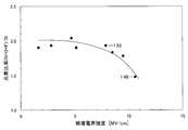
- FIG. 1An example of the relationship between the electric field strength and the current density of the silicon oxynitride film obtained by the film forming method is shown in FIG.
- the deposition conditions in this caseare as follows: the substrate 20 is a silicon substrate, the temperature of the substrate 20 is 200 ° C., and the flow rates of the respective gases constituting the source gas 28 are 50 ccm for SiF 4 , 200 ccm for N 2 , and 10 ccm for O 2 . And the pressure in the vacuum vessel 22 was 0.67 Pa.
- MISmetal-silicon oxynitride film-semiconductor
- the breakdown electric field strengthis defined as the electric field strength when the current density is 1 ⁇ 10 ⁇ 5 A / cm 2 , and the leakage current density. Is the current density when the electric field strength is 3 MV / cm.
- the breakdown electric field strength of the silicon oxynitride film obtained by the film forming methodwas about 10 MV / cm, and the leakage current density was about 1 ⁇ 10 ⁇ 8 A / cm 2 .
- the breakdown electric field strength of the conventional insulating film (SiN x or SiO 2 )is at most 6 to 8 MV / cm, and a higher breakdown electric field strength is obtained.
- the leakage current densitywas comparable to that of the conventional insulating film.
- the breakdown electric field strength of the silicon oxynitride film formed by changing the flow rate conditions of the gases SiF 4 , N 2 , and O 2 constituting the source gas 28, the discharge power for plasma generation, and the gas pressure conditions in the vacuum vessel 22An example of the relationship with the leakage current density is shown in FIG. It was confirmed that the silicon oxynitride film tends to improve (decrease) the leakage current density as the breakdown electric field strength improves (increases). This is considered due to the fact that there are few defects in the silicon oxynitride film. From this point of view, it can be said that this silicon oxynitride film is an insulating film having good characteristics.
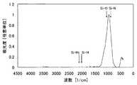
- the composition of the silicon oxynitride film obtained by the above film formation methodwas evaluated using X-ray photoelectron spectroscopy (abbreviated as XPS). As a result, it was confirmed that the obtained film was composed of silicon Si, nitrogen N, oxygen O and fluorine F. Further, the presence or absence of hydrogen in the silicon oxynitride film was confirmed by Fourier transform infrared spectroscopy (abbreviation FT-IR). The result is shown in FIG.
- FT-IRFourier transform infrared spectroscopy
- FIG. 4shows an example of the relationship between the breakdown electric field strength and the constituent element ratio when the constituent element ratio of the silicon oxynitride film obtained by the film forming method is changed.
- the constituent element ratiowas determined from the area of the peak waveform of the signal corresponding to each element obtained by XPS.
- high attached after each element symbolindicates a case where the breakdown electric field strength is 7 MV / cm or more, and low indicates a case where it is less than 7 MV / cm.
- the element ratio of silicon Si in the silicon oxynitride filmis 0.34 to 0.41
- the element ratio of nitrogen Nis 0.10 to 0.22
- the element ratio of oxygen Ois
- a high breakdown electric field strength of 7 MV / cm or more(more specifically, about 8 MV / cm or more) is obtained. It was confirmed that it was obtained. That is, it was confirmed that a silicon oxynitride film having high insulation performance can be realized by using this composition.
- the silicon oxynitride filmwhen it is considered that the silicon oxynitride film has a similar structure to the silicon oxide film, the silicon oxynitride film can be expressed as Si (O x N y F z ) R.
- the subscripts x, y, and zare the ratios of the constituent elements.
- the element ratio R(N + O + F) / Si of the total (N + O + F) of nitrogen N, oxygen O and fluorine F to silicon Si is in the range of 1.93 to 1.48, and the silicon Si in the film
- the element ratiois 0.34 to 0.41
- the nitrogen N element ratiois 0.10 to 0.22
- the oxygen O element ratiois 0.14 to 0.38
- the fluorine F element ratiois 0.17 to 0. It was confirmed that a high breakdown electric field strength of 7 MV / cm or more (more specifically, about 8 MV / cm or more) was obtained in the range of .24. That is, it was confirmed that a silicon oxynitride film having high insulation performance can be realized by using this composition.
- FIG. 1An example of the XPS spectrum of the silicon oxynitride film obtained by the film forming method is shown in FIG.
- Si--F in FIG. 6indicates that when the fluorine atom is bonded to the silicon atom, the electron bond energy of the fluorine atom has a bond energy of 685.5 eV or 687.6 eV.
- Si--F 2indicates that the binding energy of electrons of fluorine atoms is 686.8 eV when two fluorine atoms are bonded to silicon even when bonding between silicon and fluorine.
- O-Si-Findicates that when silicon, oxygen, and fluorine are bonded, the electron bond energy of the fluorine atom has a bond energy of 686.8 eV or 690.5 eV.
- the bonding state corresponding to the energy of 686.8 eVindicates that there are cases of Si -F 2 and O -Si -F.
- the bond energy value of 689 eVindicates that it appears in the case of SiN (F) —O or C—F 2 bond.
- the SiN (F) -O notationindicates that fluorine is contained in the silicon oxynitride film, and that one atom and fluorine are bonded to the bond between silicon and nitrogen.
- C—F 2indicates a case where a carbon atom and two fluorine atoms are bonded.
- FFindicates a structure in which fluorine atoms are bonded to each other. In this case, the bond energy is 696.7 eV.
- the silicon oxynitride filmdoes not contain hydrogen as can be seen from FIGS. 4 and 5 and the description thereof. Therefore, the problem that hydrogen in the film adversely affects the characteristics of the semiconductor device can be solved.
- the silicon oxynitride filmdoes not contain free fluorine as can be seen from FIG. 6 and the description thereof. Therefore, it is possible to solve the problem that free fluorine deteriorates the stability of the film quality and the film characteristics.
- the element ratio (N + O + F) / SiS of the sum of nitrogen N, oxygen O and fluorine F (N + O + F) / Si with respect to silicon Siis in the range of 1.93 to 1.48, and
- the silicon Si element ratiois 0.34 to 0.41
- the nitrogen N element ratiois 0.10 to 0.22
- the oxygen O element ratiois 0.14 to 0.38
- the fluorine F element ratiois 0.
- the silicon oxynitride filmcan be used as an insulating film or the like for semiconductor devices such as thin film transistors and MOS transistors.
- Such a semiconductor deviceis a semiconductor device having good characteristics and good characteristic stability because the silicon oxynitride film constituting the semiconductor device has the above-described features.
- the silicon oxynitride filmcan be used for a thin film transistor using an oxide semiconductor.
- An example of a structure of a thin film transistor using an oxide semiconductoris illustrated in FIG.
- This thin film transistoris an oxide semiconductor thin film transistor (abbreviated as OTFT) in which a channel layer is composed of In -Ga -Zn -O (abbreviated as IGZO) oxide semiconductor.
- An insulating film 6is formed, and a semiconductor layer 8 made of In ⁇ -Ga -Zn -O is formed on the gate insulating film 6.
- a source electrode 10 and a drain electrode 12are formed on the semiconductor layer 8 with a channel region interposed therebetween.
- An etching stopper 14 for stopping etchingis formed on the channel region.
- a protective film 16is formed on the source electrode 10, the drain electrode 12 and the etching stopper 14 to protect them.
- the hydrogenadversely affects the characteristics of the thin film transistor as described above.
- the silicon oxynitride filmwhen used as at least one of the gate insulating film 6, the etching stopper 14, and the protective film 16, the silicon oxynitride film does not contain hydrogen, and thus has good characteristics and characteristics.
- a stable oxide semiconductor thin film transistorcan be realized.
- the silicon oxynitride film according to the present inventioncan be used for semiconductor devices such as thin film transistors and MOS transistors, for example. More specifically, it can be used for a gate insulating film, an etching stopper, a protective film, and the like of a thin film transistor using an oxide semiconductor. Furthermore, such a semiconductor device can be used for displays such as a liquid crystal display and an organic EL display.
- Substrate 22Vacuum container 28
Landscapes
- Chemical & Material Sciences (AREA)
- Engineering & Computer Science (AREA)
- Physics & Mathematics (AREA)
- Chemical Kinetics & Catalysis (AREA)
- Computer Hardware Design (AREA)
- Power Engineering (AREA)
- General Physics & Mathematics (AREA)
- Manufacturing & Machinery (AREA)
- Condensed Matter Physics & Semiconductors (AREA)
- Microelectronics & Electronic Packaging (AREA)
- Mechanical Engineering (AREA)
- Inorganic Chemistry (AREA)
- General Chemical & Material Sciences (AREA)
- Materials Engineering (AREA)
- Metallurgy (AREA)
- Organic Chemistry (AREA)
- Plasma & Fusion (AREA)
- Formation Of Insulating Films (AREA)
- Thin Film Transistor (AREA)
Abstract
Description
Translated fromJapaneseこの発明は、例えば、薄膜トランジスタ、MOSトランジスタ等の半導体デバイス等に用いられるシリコン酸窒化膜およびその形成方法に関する。更には、当該シリコン酸窒化膜を有している半導体デバイスおよび酸化物半導体薄膜トランジスタに関する。The present invention relates to a silicon oxynitride film used for semiconductor devices such as thin film transistors and MOS transistors, and a method for forming the same. Furthermore, the present invention relates to a semiconductor device and an oxide semiconductor thin film transistor having the silicon oxynitride film.
非特許文献1には、In -Ga -Zn -O(略称IGZO)酸化物半導体でチャネル層を形成した酸化物半導体薄膜トランジスタ(略称OTFT)において、SiH4 /N2O混合ガスを用いたプラズマCVD法によって、保護膜(パッシベーション層)としてシリコン酸化膜(SiOx 膜)を堆積させたことが記載されている(例えば、第228頁左欄、表1参照)。Non-Patent
この非特許文献1には、酸化物半導体薄膜トランジスタの信頼性の指標の一つである、しきい値Vthがシフトした原因として、保護膜として用いたシリコン酸化膜中の水素が想定されることが記載されている(例えば、第229頁左欄参照)。This
一方、特許文献1には、従来のガス源であるSiH4 ガスに代えて、SiF4 ガスを用い、酸化ガスとしてO2 ガスを用い、キャリーガスとしてN2 ガスを用いることにより、プラズマCVD法によって、水素含有の無いシリコン酸化膜(SiO2 膜)を形成することができることが記載されている(例えば、段落0009参照)。On the other hand, in
上記のように、非特許文献1には、保護膜中の水素が、酸化物半導体薄膜トランジスタの特性に悪影響を及ぼすことが記載されており、特許文献1には、従来のガス源であるSiH4 ガスに代えてSiF4 ガスを用いることによって、水素含有の無いシリコン酸化膜を形成することができる技術が記載されているけれども、特許文献1に記載の技術にもなお課題がある。As described above, Non-Patent
それは、特許文献1に記載の技術では、シリコン酸化膜中に、水素は含まれないとしても、フッ化物から遊離したフッ素F2 が含まれることになることである。このことは、特許文献1の段落0009に(2)式として記載されている次式からも明らかである。That is, in the technique described in
[数1]
SiF4 +O2 →SiO2 +2F2 [Equation 1]
SiF4 + O2 → SiO2 + 2F2
膜中に遊離したフッ素が含まれていると、当該フッ素が膜中で動いたり、アウトガスとして膜から抜け出たりするので、膜構造の安定性が悪くなり、その結果、膜質の安定性が悪くなり、膜特性も悪くなる。If free fluorine is contained in the film, the fluorine moves in the film or escapes from the film as outgas, which deteriorates the stability of the film structure, resulting in poor film quality stability. The film characteristics also deteriorate.
そこでこの発明は、水素および遊離フッ素を含んでおらず、膜特性の良い絶縁性膜を提供することを一つの目的としている。Therefore, an object of the present invention is to provide an insulating film that does not contain hydrogen and free fluorine and has good film characteristics.
この発明に係るシリコン酸窒化膜は、シリコン、窒素、酸素およびフッ素を含んで成る膜であって、シリコンSi に対する、窒素N、酸素Oおよびフッ素Fの合計(N+O+F)の元素比率(N+O+F)/Si が1.93~1.48の範囲にあり、かつ当該膜中のシリコンの元素比率が0.34~0.41、窒素の元素比率が0.10~0.22、酸素の元素比率が0.14~0.38およびフッ素の元素比率が0.17~0.24の範囲にある、ことを特徴としている。The silicon oxynitride film according to the present invention is a film containing silicon, nitrogen, oxygen and fluorine, and the element ratio (N + O + F) / total of nitrogen N, oxygen O and fluorine F (N + O + F) / silicon Si Si is in the range of 1.93 to 1.48, the silicon element ratio in the film is 0.34 to 0.41, the nitrogen element ratio is 0.10 to 0.22, and the oxygen element ratio is It is characterized in that the element ratio of 0.14 to 0.38 and fluorine is in the range of 0.17 to 0.24.
このシリコン酸窒化膜は、水素を含んでいない。従って、膜中の水素が半導体デバイスの特性に悪影響を及ぼすという課題を解決することができる。This silicon oxynitride film does not contain hydrogen. Therefore, the problem that hydrogen in the film adversely affects the characteristics of the semiconductor device can be solved.
更にこのシリコン酸窒化膜は、遊離フッ素も含んでいない。従って、遊離フッ素が膜質の安定性を悪化させ、膜特性も悪化させるという課題を解決することができる。Furthermore, this silicon oxynitride film does not contain free fluorine. Therefore, it is possible to solve the problem that free fluorine deteriorates the stability of the film quality and the film characteristics.
しかも、各元素比率が上記範囲にあるので、このシリコン酸窒化膜は、破壊電界強度が高く、かつリーク電流密度が低く、絶縁性膜として優れている。In addition, since the ratio of each element is in the above range, this silicon oxynitride film has a high breakdown electric field strength, a low leakage current density, and is excellent as an insulating film.
このシリコン酸窒化膜は、半導体デバイスに用いても良い。より具体例を挙げると、酸化物半導体を用いた薄膜トランジスタのゲート絶縁膜、エッチングストッパ、保護膜等に用いても良い。This silicon oxynitride film may be used for a semiconductor device. As a more specific example, it may be used for a gate insulating film, an etching stopper, a protective film, or the like of a thin film transistor using an oxide semiconductor.
上記シリコン酸窒化膜は、例えば、原料ガスとして、四フッ化シリコンガス(SiF4 )、窒素ガスおよび酸素含有ガスを使用し、誘導結合によってプラズマを生成する誘導結合型のプラズマCVD法によって基板上に形成しても良い。The silicon oxynitride film is formed on the substrate by, for example, inductively coupled plasma CVD using silicon tetrafluoride gas (SiF4 ), nitrogen gas, and oxygen-containing gas as source gas and generating plasma by inductive coupling. You may form in.
請求項1に記載のシリコン酸窒化膜は、水素を含んでいない。従って、膜中の水素が半導体デバイスの特性に悪影響を及ぼすという課題を解決することができる。The silicon oxynitride film according to
更にこのシリコン酸窒化膜は、遊離フッ素も含んでいない。従って、遊離フッ素が膜質の安定性を悪化させ、膜特性も悪化させるという課題を解決することができる。Furthermore, this silicon oxynitride film does not contain free fluorine. Therefore, it is possible to solve the problem that free fluorine deteriorates the stability of the film quality and the film characteristics.
しかも、各元素比率が請求項1に記載の範囲にあるので、このシリコン酸窒化膜は、破壊電界強度が高く、かつリーク電流密度が低く、絶縁性膜として優れている。Moreover, since the ratio of each element is in the range described in
請求項2に記載の発明によれば、請求項1に記載のシリコン酸窒化膜を有しているので、特性が良く、かつ特性安定性の良い半導体デバイスを実現することができる。According to the second aspect of the present invention, since the silicon oxynitride film according to the first aspect is provided, a semiconductor device having good characteristics and good characteristic stability can be realized.
請求項3に記載の発明によれば、請求項1に記載のシリコン酸窒化膜を、ゲート絶縁膜、エッチングストッパおよび保護膜の少なくとも一つに用いているので、特性が良く、かつ特性安定性の良い酸化物半導体薄膜トランジスタを実現することができる。According to the invention described in claim 3, since the silicon oxynitride film described in
請求項4に記載の発明によれば次の効果を奏する。即ち、原料ガスとして水素を含まないガスを用いるので、水素を含んでいないシリコン酸窒化膜を形成することができる。しかも、四フッ化シリコンガス(SiF4 )および窒素ガス(N2 )は、従来から良く用いられているシラン(SiH4 )およびアンモニア(NH3 )に比べて放電分解をさせにくいけれども、誘導結合型のプラズマCVD法によれば、大きな誘導電界をプラズマ中に発生させることができるので、当該四フッ化シリコンガスおよび窒素ガスを効率良く放電分解させることができる。その結果、高密度プラズマを生成して、シリコン酸窒化膜を効率良く形成することができる。According to invention of
請求項5に記載の発明によれば、基板および膜に与える熱による悪影響を抑えつつ、特性の良いシリコン酸窒化膜を形成することができる。According to the fifth aspect of the present invention, it is possible to form a silicon oxynitride film having good characteristics while suppressing adverse effects due to heat applied to the substrate and the film.
図1に、誘導結合型のプラズマCVD法によって基板上に膜を形成する、誘導結合型のプラズマCVD装置の一例を示す。FIG. 1 shows an example of an inductively coupled plasma CVD apparatus for forming a film on a substrate by an inductively coupled plasma CVD method.
このプラズマCVD装置は、平面導体34に高周波電源42から高周波電流を流すことによって発生する誘導電界によってプラズマ40を生成し、当該プラズマ40を用いて基板20上に、プラズマCVD法によって膜形成を行う誘導結合型のプラズマCVD装置である。This plasma CVD apparatus generates
基板20は、例えば、後述する基板2(図7参照)、液晶ディスプレイや有機ELディスプレイ等のフラットパネルディスプレイ(FPD)用の基板、フレキシブルディスプレイ用のフレキシブル基板等であるが、これに限られるものではない。The
このプラズマCVD装置は、例えば金属製の真空容器22を備えており、その内部は真空排気装置24によって真空排気される。This plasma CVD apparatus is provided with, for example, a
真空容器22内には、基板20に施す処理内容に応じた原料ガス28が、ガス導入管26を通して導入される。例えば、後述するように、原料ガス28として、四フッ化シリコンガスSiF4 、窒素ガスN2 および酸素含有ガスの混合ガスが導入される。酸素含有ガスは、例えば、酸素ガスO2 であるが、二酸化窒素ガスN2O等でも良い。In the
真空容器22内には、基板20を保持するホルダ30が設けられている。このホルダ30内には、基板20を加熱するヒータ32が設けられている。A
真空容器22内に、より具体的には真空容器22の天井面23の内側に、ホルダ30の基板保持面に対向するように、平面形状が長方形の平面導体34が設けられている。この平面導体34の平面形状は、長方形でも良いし、正方形等でも良い。その平面形状を具体的にどのようなものにするかは、例えば、基板20の平面形状に応じて決めれば良い。A
高周波電源42から整合回路44を経由して、かつ給電電極36および終端電極38を経由して、平面導体34の長手方向の一端側の給電端と他端側の終端との間に高周波電力が供給され、それによって平面導体34に高周波電流が流される。高周波電源42から出力する高周波電力の周波数は、例えば、一般的な13.56MHzであるが、これに限られるものではない。High-frequency power is supplied from the high-
給電電極36および終端電極38は、絶縁フランジ39をそれぞれ介して、真空容器22の天井面23に取り付けられている。これらの要素の間には、真空シール用のパッキンがそれぞれ設けられている。天井面23の上部は、この例のように、高周波の漏洩を防止するシールドボックス46で覆っておくのが好ましい。The
上記のようにして平面導体34に高周波電流を流すことによって、平面導体34の周囲に高周波磁界が発生し、それによって高周波電流と逆方向に誘導電界が発生する。この誘導電界によって、真空容器22内において、電子が加速されて平面導体34の近傍のガス28を電離させて平面導体34の近傍にプラズマ40が発生する。このプラズマ40は基板20の近傍まで拡散し、このプラズマ40によって基板20上に、プラズマCVD法による膜形成を行うことができる。When a high-frequency current is passed through the
上記のようなプラズマCVD装置を用いた誘導結合型のプラズマCVD法によって、原料ガス28として四フッ化シリコンガスSiF4 、窒素ガスN2 および酸素ガスO2 を使用して、基板20上に、シリコンSi 、窒素N、酸素Oおよびフッ素Fを含んで成るシリコン酸窒化膜を形成した。このときの基板20の温度は100℃~300℃の範囲にするのが好ましい。なお、酸素含有ガスとして、酸素ガスO2 の代わりに、二酸化窒素ガスN2Oを使用しても良い。By using inductively coupled plasma CVD using the above plasma CVD apparatus, silicon tetrafluoride gas SiF4 , nitrogen gas N2 and oxygen gas O2 are used as
この膜形成方法によれば、原料ガス28として水素を含まないガスを用いるので、水素を含んでいないシリコン酸窒化膜を基板20上に形成することができる。しかも、四フッ化シリコンガスSiF4 および窒素ガスN2 は、従来から良く用いられているシランSiH4 およびアンモニアNH3 に比べて放電分解をさせにくいけれども、誘導結合型のプラズマCVD法によれば、大きな誘導電界をプラズマ40中に発生させることができるので、当該四フッ化シリコンガスおよび窒素ガスを効率良く放電分解させることができる。その結果、高密度プラズマ40を生成して、基板20上にシリコン酸窒化膜を効率良く形成することができる。According to this film forming method, since a gas not containing hydrogen is used as the
また、基板20の温度を上記範囲にすることにより、基板20および膜に与える熱による悪影響を抑えつつ、特性の良いシリコン酸窒化膜を形成することができる。より具体的には、後述する優れた性質を有するシリコン酸窒化膜を基板20上に形成することができる。Further, by setting the temperature of the
上記膜形成方法によって得られたシリコン酸窒化膜の、電界強度と電流密度との関係の一例を図2に示す。この場合の成膜条件は、基板20をシリコン基板とし、基板20の温度を200℃とし、原料ガス28を構成する各ガスの流量を、SiF4 が50ccm、N2 が200ccm、O2 が10ccmとし、真空容器22内の圧力を0.67Paとした。An example of the relationship between the electric field strength and the current density of the silicon oxynitride film obtained by the film forming method is shown in FIG. The deposition conditions in this case are as follows: the
そして、得られたシリコン酸窒化膜の上にアルミニウム電極を重ねて、MIS(金属-シリコン酸窒化膜-半導体)構造にして、図2に示す特性を測定した。Then, an aluminum electrode was overlaid on the obtained silicon oxynitride film to form a MIS (metal-silicon oxynitride film-semiconductor) structure, and the characteristics shown in FIG. 2 were measured.
この明細書中で採用している定義を説明すると、図2中にも示すように、破壊電界強度は、電流密度が1×10⁻⁵A/cm2 のときの電界強度とし、リーク電流密度は、電界強度が3MV/cmのときの電流密度とした。The definition adopted in this specification will be explained. As shown in FIG. 2, the breakdown electric field strength is defined as the electric field strength when the current density is 1 × 10⁻⁵ A / cm2 , and the leakage current density. Is the current density when the electric field strength is 3 MV / cm.
図2から分るように、上記膜形成方法によって得られたシリコン酸窒化膜の破壊電界強度は約10MV/cm、リーク電流密度は約1×10-8A/cm2 であった。従来の絶縁性膜(SiNx またはSiO2 )の破壊電界強度はせいぜい6~8MV/cm止まりであり、これよりも高い破壊電界強度が得られた。一方、リーク電流密度は、従来の絶縁性膜のものと同程度であった。As can be seen from FIG. 2, the breakdown electric field strength of the silicon oxynitride film obtained by the film forming method was about 10 MV / cm, and the leakage current density was about 1 × 10⁻⁸ A / cm2 . The breakdown electric field strength of the conventional insulating film (SiNx or SiO2 ) is at most 6 to 8 MV / cm, and a higher breakdown electric field strength is obtained. On the other hand, the leakage current density was comparable to that of the conventional insulating film.
上記原料ガス28を構成する各ガスSiF4 、N2 、O2 の流量条件、プラズマ生成の放電電力および真空容器22内のガス圧条件を変化させて形成したシリコン酸窒化膜の破壊電界強度とリーク電流密度との関係の一例を図3に示す。当該シリコン酸窒化膜は、破壊電界強度の改善(上昇)に伴い、リーク電流密度も改善する(減少する)傾向のあることが確認された。これは、当該シリコン酸窒化膜中の欠陥が少ないことによるものと考えられる。この観点からも、このシリコン酸窒化膜は、特性の良い絶縁性膜であると言うことができる。The breakdown electric field strength of the silicon oxynitride film formed by changing the flow rate conditions of the gases SiF4 , N2 , and O2 constituting the
上記膜形成方法によって得られたシリコン酸窒化膜の組成を、X線光電子分光(略称XPS)を用いて評価した。その結果、得られた膜は、シリコンSi 、窒素N、酸素Oおよびフッ素Fで構成されていることが確認された。更に当該シリコン酸窒化膜中の水素の有無をフーリエ変換型赤外分光法(略称FT-IR)によって確認した。その結果を図8に示す。この赤外吸収スペクトルに示すように、Si -H(波数2000/cm)およびSi -H2 (波数2100/cm)による赤外吸収ピークは観られないので、上記シリコン酸窒化膜中に水素は含まれていないことが確認できた。The composition of the silicon oxynitride film obtained by the above film formation method was evaluated using X-ray photoelectron spectroscopy (abbreviated as XPS). As a result, it was confirmed that the obtained film was composed of silicon Si, nitrogen N, oxygen O and fluorine F. Further, the presence or absence of hydrogen in the silicon oxynitride film was confirmed by Fourier transform infrared spectroscopy (abbreviation FT-IR). The result is shown in FIG. As shown in the infrared absorption spectrum, since Si -H (wave number 2000 / cm) and Si -H2 infrared absorption peak due to (wavenumber 2100 / cm) is not seen, hydrogen in the silicon oxynitride film It was confirmed that it was not included.
上記膜形成方法によって得られるシリコン酸窒化膜の構成元素比率を変えたときの、破壊電界強度と構成元素比率との関係の一例を図4に示す。構成元素比率は、XPSで得られた各元素に対応する信号のピーク波形の面積から決定した。図中の各元素記号の後ろに付したhighは破壊電界強度が7MV/cm以上である場合を示し、lowは7MV/cm未満である場合を示す。FIG. 4 shows an example of the relationship between the breakdown electric field strength and the constituent element ratio when the constituent element ratio of the silicon oxynitride film obtained by the film forming method is changed. The constituent element ratio was determined from the area of the peak waveform of the signal corresponding to each element obtained by XPS. In the figure, high attached after each element symbol indicates a case where the breakdown electric field strength is 7 MV / cm or more, and low indicates a case where it is less than 7 MV / cm.
この図4から分るように、上記シリコン酸窒化膜中のシリコンSi の元素比率が0.34~0.41、窒素Nの元素比率が0.10~0.22、酸素Oの元素比率が0.14~0.38およびフッ素Fの元素比率が0.17~0.24の範囲にある場合に、7MV/cm以上(より具体的には約8MV/cm以上)という高い破壊電界強度が得られることが確認できた。即ち、この組成にすることによって、絶縁性能の高いシリコン酸窒化膜を実現することができることが確認できた。As can be seen from FIG. 4, the element ratio of silicon Si in the silicon oxynitride film is 0.34 to 0.41, the element ratio of nitrogen N is 0.10 to 0.22, and the element ratio of oxygen O is When the element ratio of 0.14 to 0.38 and fluorine F is in the range of 0.17 to 0.24, a high breakdown electric field strength of 7 MV / cm or more (more specifically, about 8 MV / cm or more) is obtained. It was confirmed that it was obtained. That is, it was confirmed that a silicon oxynitride film having high insulation performance can be realized by using this composition.
一方、上記シリコン酸窒化膜がシリコン酸化膜と類似の構造を有するものと考えると、当該シリコン酸窒化膜はSi(Ox Ny Fz ) R と表すことができる。添字のx、y、zは各構成元素の比率である。Rは、Si に対する(N+O+F)の元素比率であり、R=(N+O+F)/Si で表すこともできる。On the other hand, when it is considered that the silicon oxynitride film has a similar structure to the silicon oxide film, the silicon oxynitride film can be expressed as Si (Ox Ny Fz )R. The subscripts x, y, and z are the ratios of the constituent elements. R is an element ratio of (N + O + F) to Si, and can also be represented by R = (N + O + F) / Si.
上記膜形成方法によって得られたシリコン酸窒化膜の、破壊電界強度と元素比率R=(N+O+F)/Si との関係の一例を図5に示す。FIG. 5 shows an example of the relationship between the breakdown electric field strength and the element ratio R = (N + O + F) / Si in the silicon oxynitride film obtained by the film forming method.
この図5から分るように、元素比率R=(N+O+F)/Si が約2付近から小さくなるのに従って、破壊電界強度が上昇することが確認できた。特に、R=(N+O+F)/Si が1.93~1.48の範囲で、7MV/cm以上(より具体的には約8MV/cm以上)という高い破壊電界強度を得ることができた。但し、Rが1.93付近では破壊電界強度が低い場合もあるが、このRの条件と、図4に示した各元素の元素比率の条件とを組み合わせることによって、破壊電界強度が高くて、絶縁性能の高いシリコン酸窒化膜を実現することができる。As can be seen from FIG. 5, it was confirmed that the breakdown electric field strength increased as the element ratio R = (N + O + F) / Si decreased from around 2. In particular, a high breakdown field strength of 7 MV / cm or more (more specifically, about 8 MV / cm or more) was obtained when R = (N + O + F) / Si / was in the range of 1.93 to 1.48. However, there are cases where the breakdown electric field strength is low near R of 1.93, but by combining the conditions of R with the element ratio conditions of each element shown in FIG. A silicon oxynitride film having high insulation performance can be realized.
即ち、シリコンSi に対する、窒素N、酸素Oおよびフッ素Fの合計(N+O+F)の元素比率R=(N+O+F)/Si が1.93~1.48の範囲にあり、かつ当該膜中のシリコンSi の元素比率が0.34~0.41、窒素Nの元素比率が0.10~0.22、酸素Oの元素比率が0.14~0.38およびフッ素Fの元素比率が0.17~0.24の範囲にある場合に、7MV/cm以上(より具体的には約8MV/cm以上)という高い破壊電界強度が得られることが確認できた。即ち、この組成にすることによって、絶縁性能の高いシリコン酸窒化膜を実現することができることが確認できた。That is, the element ratio R = (N + O + F) / Si of the total (N + O + F) of nitrogen N, oxygen O and fluorine F to silicon Si is in the range of 1.93 to 1.48, and the silicon Si in the film The element ratio is 0.34 to 0.41, the nitrogen N element ratio is 0.10 to 0.22, the oxygen O element ratio is 0.14 to 0.38, and the fluorine F element ratio is 0.17 to 0. It was confirmed that a high breakdown electric field strength of 7 MV / cm or more (more specifically, about 8 MV / cm or more) was obtained in the range of .24. That is, it was confirmed that a silicon oxynitride film having high insulation performance can be realized by using this composition.
上記膜形成方法によって得られたシリコン酸窒化膜のXPSスペクトルの一例を図6に示す。An example of the XPS spectrum of the silicon oxynitride film obtained by the film forming method is shown in FIG.
図6中のSi -Fは、フッ素原子がシリコン原子と結合した場合に、フッ素原子の電子の結合エネルギーが685.5eVまたは687.6eVの結合エネルギーを有することを示している。Si -F2 は、シリコンとフッ素の結合でもシリコンにフッ素が2個結合した場合の、フッ素原子の電子の結合エネルギーは686.8eVであることを示している。O-Si -Fは、シリコン、酸素およびフッ素が結合した場合の、フッ素原子の電子の結合エネルギーは686.8eVまたは690.5eVの結合エネルギーを有することを示している。逆に、686.8eVのエネルギーに相当する結合状態は、Si -F2 の場合とO-Si -Fの場合があることを示している。689eVの結合エネルギーの値は、SiN(F)-OまたはC-F2 の結合の場合に現れることを示している。SiN(F)-Oの表記ではシリコン酸窒化膜中にフッ素が入っており、シリコンと窒素の結合に対してどちらかの原子とフッ素が結合した状態にあることを示している。また、C-F2 は、炭素原子とフッ素原子2個が結合した場合を示している。F-Fは、フッ素原子同士が結合した構造を示しており、その場合696.7eVの結合エネルギーであることを示している。Si--F in FIG. 6 indicates that when the fluorine atom is bonded to the silicon atom, the electron bond energy of the fluorine atom has a bond energy of 685.5 eV or 687.6 eV. Si--F2 indicates that the binding energy of electrons of fluorine atoms is 686.8 eV when two fluorine atoms are bonded to silicon even when bonding between silicon and fluorine. O-Si-F indicates that when silicon, oxygen, and fluorine are bonded, the electron bond energy of the fluorine atom has a bond energy of 686.8 eV or 690.5 eV. On the contrary, the bonding state corresponding to the energy of 686.8 eV indicates that there are cases of Si -F2 and O -Si -F. The bond energy value of 689 eV indicates that it appears in the case of SiN (F) —O or C—F2 bond. The SiN (F) -O notation indicates that fluorine is contained in the silicon oxynitride film, and that one atom and fluorine are bonded to the bond between silicon and nitrogen. C—F2 indicates a case where a carbon atom and two fluorine atoms are bonded. FF indicates a structure in which fluorine atoms are bonded to each other. In this case, the bond energy is 696.7 eV.
このXPSスペクトルから分るように、F-Fの結合エネルギー696.7eVに山は観られないので、上記シリコン酸窒化膜中に遊離フッ素は含まれていないと判断することができる。As can be seen from this XPS spectrum, no peaks are observed in the FF bond energy of 696.7 eV, so it can be determined that the silicon oxynitride film does not contain free fluorine.
以上をまとめると、上記シリコン酸窒化膜は、図4、図5およびその説明等からも分るように、水素を含んでいない。従って、膜中の水素が半導体デバイスの特性に悪影響を及ぼすという課題を解決することができる。In summary, the silicon oxynitride film does not contain hydrogen as can be seen from FIGS. 4 and 5 and the description thereof. Therefore, the problem that hydrogen in the film adversely affects the characteristics of the semiconductor device can be solved.
更に上記シリコン酸窒化膜は、図6およびその説明からも分るように、遊離フッ素も含んでいない。従って、遊離フッ素が膜質の安定性を悪化させ、膜特性も悪化させるという課題を解決することができる。Furthermore, the silicon oxynitride film does not contain free fluorine as can be seen from FIG. 6 and the description thereof. Therefore, it is possible to solve the problem that free fluorine deteriorates the stability of the film quality and the film characteristics.
しかも、上記シリコン酸窒化膜において、シリコンSi に対する、窒素N、酸素Oおよびフッ素Fの合計(N+O+F)の元素比率(N+O+F)/Si を1.93~1.48の範囲にし、かつ当該膜中のシリコンSi の元素比率を0.34~0.41、窒素Nの元素比率を0.10~0.22、酸素Oの元素比率を0.14~0.38およびフッ素Fの元素比率を0.17~0.24の範囲にすることによって、破壊電界強度が高く、かつリーク電流密度が低く、絶縁性膜として優れているシリコン酸窒化膜を実現することができる。Moreover, in the silicon oxynitride film, the element ratio (N + O + F) / SiS of the sum of nitrogen N, oxygen O and fluorine F (N + O + F) / Si with respect to silicon Si is in the range of 1.93 to 1.48, and The silicon Si element ratio is 0.34 to 0.41, the nitrogen N element ratio is 0.10 to 0.22, the oxygen O element ratio is 0.14 to 0.38, and the fluorine F element ratio is 0. By setting the thickness within the range of .17 to 0.24, it is possible to realize a silicon oxynitride film having a high breakdown electric field strength and a low leakage current density and excellent as an insulating film.
上記シリコン酸窒化膜は、例えば薄膜トランジスタ、MOSトランジスタ等の半導体デバイスに、絶縁性膜等として用いることができる。そのような半導体デバイスは、それを構成するシリコン酸窒化膜が上記のような特長を有しているので、特性が良く、かつ特性安定性の良い半導体デバイスになる。The silicon oxynitride film can be used as an insulating film or the like for semiconductor devices such as thin film transistors and MOS transistors. Such a semiconductor device is a semiconductor device having good characteristics and good characteristic stability because the silicon oxynitride film constituting the semiconductor device has the above-described features.
より具体例を挙げると、上記シリコン酸窒化膜は、酸化物半導体を用いた薄膜トランジスタに用いることができる。酸化物半導体を用いた薄膜トランジスタの構成の一例を図7に示す。More specifically, the silicon oxynitride film can be used for a thin film transistor using an oxide semiconductor. An example of a structure of a thin film transistor using an oxide semiconductor is illustrated in FIG.
この薄膜トランジスタは、In -Ga -Zn -O(略称IGZO)酸化物半導体でチャネル層を構成した酸化物半導体薄膜トランジスタ(略称OTFT)であり、基板(例えばガラス基板)2の上にゲート電極4およびゲート絶縁膜6が形成されており、ゲート絶縁膜6上に、In -Ga -Zn -Oから成る半導体層8が形成されている。この半導体層8の上に、チャネル領域を挟んでソース電極10およびドレイン電極12が形成されている。チャネル領域上には、エッチングを止めるエッチングストッパ14が形成されている。更に、ソース電極10、ドレイン電極12およびエッチングストッパ14の上に、これらを保護する保護膜16が形成されている。This thin film transistor is an oxide semiconductor thin film transistor (abbreviated as OTFT) in which a channel layer is composed of In -Ga -Zn -O (abbreviated as IGZO) oxide semiconductor. An insulating
このような酸化物半導体薄膜トランジスタにおいて、そのゲート絶縁膜6、エッチングストッパ14または保護膜16が水素を含有していると、前述したように、当該水素が当該薄膜トランジスタの特性に悪影響を及ぼす。In such an oxide semiconductor thin film transistor, when the
そこで、このゲート絶縁膜6、エッチングストッパ14および保護膜16の少なくとも一つに、上記シリコン酸窒化膜を用いると、当該シリコン酸窒化膜は水素を含有していないので、特性が良く、かつ特性安定性の良い酸化物半導体薄膜トランジスタを実現することができる。Therefore, when the silicon oxynitride film is used as at least one of the
この発明に係るシリコン酸窒化膜は、例えば、薄膜トランジスタ、MOSトランジスタ等の半導体デバイス等に用いることができる。より具体例を挙げると、酸化物半導体を用いた薄膜トランジスタのゲート絶縁膜、エッチングストッパ、保護膜等に用いることができる。更にこのような半導体デバイスは、例えば、液晶ディスプレイ、有機ELディスプレイ等のディスプレイ等に用いることができる。The silicon oxynitride film according to the present invention can be used for semiconductor devices such as thin film transistors and MOS transistors, for example. More specifically, it can be used for a gate insulating film, an etching stopper, a protective film, and the like of a thin film transistor using an oxide semiconductor. Furthermore, such a semiconductor device can be used for displays such as a liquid crystal display and an organic EL display.
20 基板
22 真空容器
28 原料ガス
30 ホルダ
34 平面導体
40 プラズマ
42 高周波電源20
Claims (5)
Translated fromJapaneseシリコンSi に対する、窒素N、酸素Oおよびフッ素Fの合計(N+O+F)の元素比率(N+O+F)/Si が1.93~1.48の範囲にあり、
かつ当該膜中のシリコンの元素比率が0.34~0.41、窒素の元素比率が0.10~0.22、酸素の元素比率が0.14~0.38およびフッ素の元素比率が0.17~0.24の範囲にある、ことを特徴とするシリコン酸窒化膜。A silicon oxynitride film comprising silicon, nitrogen, oxygen and fluorine,
The ratio (N + O + F) / Si of the sum of nitrogen N, oxygen O and fluorine F (N + O + F) / Si with respect to silicon Si is in the range of 1.93 to 1.48.
The element ratio of silicon in the film is 0.34 to 0.41, the element ratio of nitrogen is 0.10 to 0.22, the element ratio of oxygen is 0.14 to 0.38, and the element ratio of fluorine is 0. A silicon oxynitride film characterized by being in the range of .17 to 0.24.
Priority Applications (5)
| Application Number | Priority Date | Filing Date | Title |
|---|---|---|---|
| PCT/JP2010/007137WO2012077163A1 (en) | 2010-12-08 | 2010-12-08 | Silicon oxynitride film and method for forming same, and semiconductor device |
| KR1020137003191AKR101475899B1 (en) | 2010-12-08 | 2010-12-08 | Silicon oxynitride film and method for forming same, and semiconductor device |
| JP2012547601AJP5224012B2 (en) | 2010-12-08 | 2010-12-08 | Method for forming silicon oxynitride film and semiconductor device |
| CN201080069030.8ACN103098187B (en) | 2010-12-08 | 2010-12-08 | Silicon oxynitride film and method for forming same, semiconductor device and thin film transistor |
| US13/823,108US9058982B2 (en) | 2010-12-08 | 2010-12-08 | Silicon oxynitride film and method for forming same, and semiconductor device |
Applications Claiming Priority (1)
| Application Number | Priority Date | Filing Date | Title |
|---|---|---|---|
| PCT/JP2010/007137WO2012077163A1 (en) | 2010-12-08 | 2010-12-08 | Silicon oxynitride film and method for forming same, and semiconductor device |
Publications (1)
| Publication Number | Publication Date |
|---|---|
| WO2012077163A1true WO2012077163A1 (en) | 2012-06-14 |
Family
ID=46206685
Family Applications (1)
| Application Number | Title | Priority Date | Filing Date |
|---|---|---|---|
| PCT/JP2010/007137WO2012077163A1 (en) | 2010-12-08 | 2010-12-08 | Silicon oxynitride film and method for forming same, and semiconductor device |
Country Status (5)
| Country | Link |
|---|---|
| US (1) | US9058982B2 (en) |
| JP (1) | JP5224012B2 (en) |
| KR (1) | KR101475899B1 (en) |
| CN (1) | CN103098187B (en) |
| WO (1) | WO2012077163A1 (en) |
Cited By (5)
| Publication number | Priority date | Publication date | Assignee | Title |
|---|---|---|---|---|
| JP2015018889A (en)* | 2013-07-10 | 2015-01-29 | 日新電機株式会社 | Thin film transistor manufacturing method |
| JP2016510171A (en)* | 2013-03-01 | 2016-04-04 | アプライド マテリアルズ インコーポレイテッドApplied Materials,Incorporated | Improved stability of metal oxide TFT |
| JP2016072570A (en)* | 2014-10-01 | 2016-05-09 | 東京エレクトロン株式会社 | Electronic device, manufacturing method thereof, and manufacturing apparatus thereof |
| JP2016082241A (en)* | 2014-10-20 | 2016-05-16 | 株式会社半導体エネルギー研究所 | Semiconductor device, manufacturing method thereof, module, and electronic apparatus |
| KR20180077277A (en) | 2015-12-08 | 2018-07-06 | 고쿠리츠다이가쿠호징 나라 센탄카가쿠기쥬츠 다이가쿠인 다이가쿠 | Thin film transistor, method of manufacturing the same, and semiconductor device having the thin film transistor |
Families Citing this family (2)
| Publication number | Priority date | Publication date | Assignee | Title |
|---|---|---|---|---|
| KR101582838B1 (en)* | 2013-08-23 | 2016-01-12 | 니신 일렉트릭 컴패니 리미티드 | Plasma processing apparatus |
| JP5790893B1 (en)* | 2015-02-13 | 2015-10-07 | 日新電機株式会社 | Film forming method and thin film transistor manufacturing method |
Citations (4)
| Publication number | Priority date | Publication date | Assignee | Title |
|---|---|---|---|---|
| JPH0878408A (en)* | 1994-09-08 | 1996-03-22 | Fujitsu Ltd | Method for manufacturing semiconductor device |
| JPH1012611A (en)* | 1996-06-26 | 1998-01-16 | Sony Corp | Passivation film for protecting wiring and manufacture of semiconductor device |
| JP2003060030A (en)* | 2001-08-10 | 2003-02-28 | Hitachi Ltd | Semiconductor integrated circuit device and manufacturing method thereof |
| JP2009076886A (en)* | 2007-08-24 | 2009-04-09 | Semiconductor Energy Lab Co Ltd | Method for manufacturing semiconductor device |
Family Cites Families (26)
| Publication number | Priority date | Publication date | Assignee | Title |
|---|---|---|---|---|
| JPH0529301A (en) | 1991-07-23 | 1993-02-05 | Seiko Epson Corp | CVD method |
| EP0723944A1 (en)* | 1995-01-26 | 1996-07-31 | Optical Coating Laboratory, Inc. | Wear resistant windows |
| US6362114B1 (en)* | 1996-11-12 | 2002-03-26 | Micron Technology, Inc. | Semiconductor processing methods of forming an oxynitride film on a silicon substrate |
| JPH10154712A (en)* | 1996-11-25 | 1998-06-09 | Fujitsu Ltd | Method for manufacturing semiconductor device |
| US6184158B1 (en)* | 1996-12-23 | 2001-02-06 | Lam Research Corporation | Inductively coupled plasma CVD |
| FR2759362B1 (en)* | 1997-02-10 | 1999-03-12 | Saint Gobain Vitrage | TRANSPARENT SUBSTRATE EQUIPPED WITH AT LEAST ONE THIN LAYER BASED ON SILICON NITRIDE OR OXYNITRIDE AND ITS PROCESS FOR OBTAINING IT |
| US5872065A (en)* | 1997-04-02 | 1999-02-16 | Applied Materials Inc. | Method for depositing low K SI-O-F films using SIF4 /oxygen chemistry |
| US6077764A (en)* | 1997-04-21 | 2000-06-20 | Applied Materials, Inc. | Process for depositing high deposition rate halogen-doped silicon oxide layer |
| GB2373372B (en)* | 1999-11-30 | 2004-04-28 | Intel Corp | Improved flourine doped sio2 film |
| US6472336B1 (en)* | 2000-02-23 | 2002-10-29 | Advanced Micro Devices, Inc. | Forming an encapsulating layer after deposition of a dielectric comprised of corrosive material |
| US6468927B1 (en)* | 2000-05-19 | 2002-10-22 | Applied Materials, Inc. | Method of depositing a nitrogen-doped FSG layer |
| US7074489B2 (en)* | 2001-05-23 | 2006-07-11 | Air Products And Chemicals, Inc. | Low dielectric constant material and method of processing by CVD |
| JP3746968B2 (en)* | 2001-08-29 | 2006-02-22 | 東京エレクトロン株式会社 | Insulating film forming method and forming system |
| US20070184181A1 (en)* | 2003-03-25 | 2007-08-09 | Kazuo Wada | Device and method for forming film for organic electro-luminescence element using inductive coupling CVD |
| US7378157B2 (en)* | 2004-06-28 | 2008-05-27 | Dai Nippon Printing Co., Ltd. | Gas barrier film, and display substrate and display using the same |
| US20060017166A1 (en)* | 2004-07-20 | 2006-01-26 | Po-Hsiung Leu | Robust fluorine containing Silica Glass (FSG) Film with less free fluorine |
| US7037855B2 (en)* | 2004-08-31 | 2006-05-02 | Asm Japan K.K. | Method of forming fluorine-doped low-dielectric-constant insulating film |
| US20060071301A1 (en)* | 2004-10-06 | 2006-04-06 | Luo Shing A | Silicon rich dielectric antireflective coating |
| KR100669142B1 (en)* | 2005-04-20 | 2007-01-15 | (주)더리즈 | Light emitting device and manufacturing method thereof |
| KR100700493B1 (en)* | 2005-05-24 | 2007-03-28 | 삼성에스디아이 주식회사 | Catalytically Enhanced Chemical Vapor Deposition Equipment with Efficient Filament Array Structure |
| JP4717674B2 (en)* | 2006-03-27 | 2011-07-06 | 富士フイルム株式会社 | Gas barrier film, substrate film and organic electroluminescence device |
| US20070299239A1 (en)* | 2006-06-27 | 2007-12-27 | Air Products And Chemicals, Inc. | Curing Dielectric Films Under A Reducing Atmosphere |
| JP2008300779A (en)* | 2007-06-04 | 2008-12-11 | Elpida Memory Inc | Semiconductor device and manufacturing method thereof |
| DE102008028141A1 (en)* | 2008-06-13 | 2009-12-17 | Audi Ag | glass product |
| US8174021B2 (en)* | 2009-02-06 | 2012-05-08 | Semiconductor Energy Laboratory Co., Ltd. | Semiconductor device and method of manufacturing the semiconductor device |
| CN103730515B (en)* | 2009-03-09 | 2016-08-17 | 株式会社半导体能源研究所 | Semiconductor device |
- 2010
- 2010-12-08WOPCT/JP2010/007137patent/WO2012077163A1/enactiveApplication Filing
- 2010-12-08JPJP2012547601Apatent/JP5224012B2/enactiveActive
- 2010-12-08CNCN201080069030.8Apatent/CN103098187B/enactiveActive
- 2010-12-08USUS13/823,108patent/US9058982B2/enactiveActive
- 2010-12-08KRKR1020137003191Apatent/KR101475899B1/enactiveActive
Patent Citations (4)
| Publication number | Priority date | Publication date | Assignee | Title |
|---|---|---|---|---|
| JPH0878408A (en)* | 1994-09-08 | 1996-03-22 | Fujitsu Ltd | Method for manufacturing semiconductor device |
| JPH1012611A (en)* | 1996-06-26 | 1998-01-16 | Sony Corp | Passivation film for protecting wiring and manufacture of semiconductor device |
| JP2003060030A (en)* | 2001-08-10 | 2003-02-28 | Hitachi Ltd | Semiconductor integrated circuit device and manufacturing method thereof |
| JP2009076886A (en)* | 2007-08-24 | 2009-04-09 | Semiconductor Energy Lab Co Ltd | Method for manufacturing semiconductor device |
Cited By (6)
| Publication number | Priority date | Publication date | Assignee | Title |
|---|---|---|---|---|
| JP2016510171A (en)* | 2013-03-01 | 2016-04-04 | アプライド マテリアルズ インコーポレイテッドApplied Materials,Incorporated | Improved stability of metal oxide TFT |
| JP2015018889A (en)* | 2013-07-10 | 2015-01-29 | 日新電機株式会社 | Thin film transistor manufacturing method |
| JP2016072570A (en)* | 2014-10-01 | 2016-05-09 | 東京エレクトロン株式会社 | Electronic device, manufacturing method thereof, and manufacturing apparatus thereof |
| JP2016082241A (en)* | 2014-10-20 | 2016-05-16 | 株式会社半導体エネルギー研究所 | Semiconductor device, manufacturing method thereof, module, and electronic apparatus |
| KR20180077277A (en) | 2015-12-08 | 2018-07-06 | 고쿠리츠다이가쿠호징 나라 센탄카가쿠기쥬츠 다이가쿠인 다이가쿠 | Thin film transistor, method of manufacturing the same, and semiconductor device having the thin film transistor |
| US10475934B2 (en) | 2015-12-08 | 2019-11-12 | National University Corporation NARA Institute of Science and Technology | Thin film transistor, method for manufacturing same and semiconductor device comprising said thin film transistor |
Also Published As
| Publication number | Publication date |
|---|---|
| CN103098187B (en) | 2015-09-09 |
| CN103098187A (en) | 2013-05-08 |
| US9058982B2 (en) | 2015-06-16 |
| JPWO2012077163A1 (en) | 2014-05-19 |
| KR101475899B1 (en) | 2014-12-24 |
| US20130181291A1 (en) | 2013-07-18 |
| JP5224012B2 (en) | 2013-07-03 |
| KR20130050352A (en) | 2013-05-15 |
Similar Documents
| Publication | Publication Date | Title |
|---|---|---|
| JP5224012B2 (en) | Method for forming silicon oxynitride film and semiconductor device | |
| CN104271797B (en) | Barrier materials for display devices | |
| CN101743631B (en) | Boron derived materials deposition method | |
| US9343317B2 (en) | Methods of forming silicon-containing dielectric materials and semiconductor device structures | |
| Kamiyama et al. | Comparison between SiO2 films deposited by atomic layer deposition with SiH2 [N (CH3) 2] 2 and SiH [N (CH3) 2] 3 precursors | |
| US20120220139A1 (en) | Method of depositing dielectric film by modified peald method | |
| TWI747910B (en) | Film formation method and TFT manufacturing method | |
| TW200422424A (en) | Low temperature deposition of silicon oxides and oxynitrides | |
| CN102171799A (en) | Silicon oxide film, method for forming silicon oxide film, and plasma CVD apparatus | |
| KR20090063170A (en) | Silicon Nitride Film Deposition Method | |
| JP2007287890A (en) | Insulating film forming method, semiconductor device manufacturing method, plasma CVD apparatus | |
| CN104250724A (en) | Forming method of multi-layer protective film and forming device of multi-layer protective film | |
| JP2017147438A (en) | Method of improving adhesion | |
| Kim et al. | Electrical properties of low-temperature SiO2 thin films prepared by plasma-enhanced atomic layer deposition with different plasma times | |
| da Silva Zambom et al. | Silicon nitride deposited by inductively coupled plasma using silane and nitrogen | |
| JP5790893B1 (en) | Film forming method and thin film transistor manufacturing method | |
| JPWO2018150452A1 (en) | Nitride film formation method | |
| WO2010038887A1 (en) | Silicon dioxide film and process for production thereof, computer-readable storage medium, and plasma cvd device | |
| JPWO2021186297A5 (en) | ||
| TW565893B (en) | Semiconductor device and method for producing the same | |
| US10475934B2 (en) | Thin film transistor, method for manufacturing same and semiconductor device comprising said thin film transistor | |
| JP2008078253A (en) | Manufacturing method of semiconductor device | |
| Meitine et al. | Low temperature PECVD silicon oxide for devices and circuits on flexible substrates | |
| JP2008078512A (en) | Manufacturing method of semiconductor devices | |
| TW406308B (en) | Method of manufacturing semiconductor devices |
Legal Events
| Date | Code | Title | Description |
|---|---|---|---|
| WWE | Wipo information: entry into national phase | Ref document number:201080069030.8 Country of ref document:CN | |
| 121 | Ep: the epo has been informed by wipo that ep was designated in this application | Ref document number:10860603 Country of ref document:EP Kind code of ref document:A1 | |
| WWE | Wipo information: entry into national phase | Ref document number:2012547601 Country of ref document:JP | |
| ENP | Entry into the national phase | Ref document number:20137003191 Country of ref document:KR Kind code of ref document:A | |
| WWE | Wipo information: entry into national phase | Ref document number:13823108 Country of ref document:US | |
| NENP | Non-entry into the national phase | Ref country code:DE | |
| 122 | Ep: pct application non-entry in european phase | Ref document number:10860603 Country of ref document:EP Kind code of ref document:A1 |