WO2012056615A1 - Semiconductor device - Google Patents
Semiconductor deviceDownload PDFInfo
- Publication number
- WO2012056615A1 WO2012056615A1PCT/JP2011/004147JP2011004147WWO2012056615A1WO 2012056615 A1WO2012056615 A1WO 2012056615A1JP 2011004147 WJP2011004147 WJP 2011004147WWO 2012056615 A1WO2012056615 A1WO 2012056615A1
- Authority
- WO
- WIPO (PCT)
- Prior art keywords
- wiring
- impurity diffusion
- diffusion region
- semiconductor device
- power supply
- Prior art date
Links
Images


Classifications
- H—ELECTRICITY
- H10—SEMICONDUCTOR DEVICES; ELECTRIC SOLID-STATE DEVICES NOT OTHERWISE PROVIDED FOR
- H10D—INORGANIC ELECTRIC SEMICONDUCTOR DEVICES
- H10D84/00—Integrated devices formed in or on semiconductor substrates that comprise only semiconducting layers, e.g. on Si wafers or on GaAs-on-Si wafers
- H10D84/90—Masterslice integrated circuits
- H10D84/903—Masterslice integrated circuits comprising field effect technology
- H10D84/907—CMOS gate arrays
- H—ELECTRICITY
- H01—ELECTRIC ELEMENTS
- H01L—SEMICONDUCTOR DEVICES NOT COVERED BY CLASS H10
- H01L21/00—Processes or apparatus adapted for the manufacture or treatment of semiconductor or solid state devices or of parts thereof
- H01L21/70—Manufacture or treatment of devices consisting of a plurality of solid state components formed in or on a common substrate or of parts thereof; Manufacture of integrated circuit devices or of parts thereof
- H01L21/71—Manufacture of specific parts of devices defined in group H01L21/70
- H01L21/768—Applying interconnections to be used for carrying current between separate components within a device comprising conductors and dielectrics
- H01L21/76838—Applying interconnections to be used for carrying current between separate components within a device comprising conductors and dielectrics characterised by the formation and the after-treatment of the conductors
- H01L21/76895—Local interconnects; Local pads, as exemplified by patent document EP0896365
- H—ELECTRICITY
- H01—ELECTRIC ELEMENTS
- H01L—SEMICONDUCTOR DEVICES NOT COVERED BY CLASS H10
- H01L23/00—Details of semiconductor or other solid state devices
- H01L23/48—Arrangements for conducting electric current to or from the solid state body in operation, e.g. leads, terminal arrangements ; Selection of materials therefor
- H01L23/482—Arrangements for conducting electric current to or from the solid state body in operation, e.g. leads, terminal arrangements ; Selection of materials therefor consisting of lead-in layers inseparably applied to the semiconductor body (electrodes)
- H01L23/485—Arrangements for conducting electric current to or from the solid state body in operation, e.g. leads, terminal arrangements ; Selection of materials therefor consisting of lead-in layers inseparably applied to the semiconductor body (electrodes) consisting of layered constructions comprising conductive layers and insulating layers, e.g. planar contacts
- H—ELECTRICITY
- H10—SEMICONDUCTOR DEVICES; ELECTRIC SOLID-STATE DEVICES NOT OTHERWISE PROVIDED FOR
- H10D—INORGANIC ELECTRIC SEMICONDUCTOR DEVICES
- H10D62/00—Semiconductor bodies, or regions thereof, of devices having potential barriers
- H10D62/10—Shapes, relative sizes or dispositions of the regions of the semiconductor bodies; Shapes of the semiconductor bodies
- H10D62/17—Semiconductor regions connected to electrodes not carrying current to be rectified, amplified or switched, e.g. channel regions
- H10D62/351—Substrate regions of field-effect devices
- H10D62/357—Substrate regions of field-effect devices of FETs
- H10D62/364—Substrate regions of field-effect devices of FETs of IGFETs
- H—ELECTRICITY
- H10—SEMICONDUCTOR DEVICES; ELECTRIC SOLID-STATE DEVICES NOT OTHERWISE PROVIDED FOR
- H10D—INORGANIC ELECTRIC SEMICONDUCTOR DEVICES
- H10D89/00—Aspects of integrated devices not covered by groups H10D84/00 - H10D88/00
- H10D89/10—Integrated device layouts
- H—ELECTRICITY
- H01—ELECTRIC ELEMENTS
- H01L—SEMICONDUCTOR DEVICES NOT COVERED BY CLASS H10
- H01L2924/00—Indexing scheme for arrangements or methods for connecting or disconnecting semiconductor or solid-state bodies as covered by H01L24/00
- H01L2924/0001—Technical content checked by a classifier
- H01L2924/0002—Not covered by any one of groups H01L24/00, H01L24/00 and H01L2224/00
- H—ELECTRICITY
- H10—SEMICONDUCTOR DEVICES; ELECTRIC SOLID-STATE DEVICES NOT OTHERWISE PROVIDED FOR
- H10D—INORGANIC ELECTRIC SEMICONDUCTOR DEVICES
- H10D84/00—Integrated devices formed in or on semiconductor substrates that comprise only semiconducting layers, e.g. on Si wafers or on GaAs-on-Si wafers
- H10D84/90—Masterslice integrated circuits
- H10D84/903—Masterslice integrated circuits comprising field effect technology
- H10D84/907—CMOS gate arrays
- H10D84/909—Microarchitecture
- H10D84/929—Isolations
- H—ELECTRICITY
- H10—SEMICONDUCTOR DEVICES; ELECTRIC SOLID-STATE DEVICES NOT OTHERWISE PROVIDED FOR
- H10D—INORGANIC ELECTRIC SEMICONDUCTOR DEVICES
- H10D84/00—Integrated devices formed in or on semiconductor substrates that comprise only semiconducting layers, e.g. on Si wafers or on GaAs-on-Si wafers
- H10D84/90—Masterslice integrated circuits
- H10D84/903—Masterslice integrated circuits comprising field effect technology
- H10D84/907—CMOS gate arrays
- H10D84/909—Microarchitecture
- H10D84/959—Connectability characteristics, i.e. diffusion and polysilicon geometries
- H10D84/961—Substrate and well contacts
- H—ELECTRICITY
- H10—SEMICONDUCTOR DEVICES; ELECTRIC SOLID-STATE DEVICES NOT OTHERWISE PROVIDED FOR
- H10D—INORGANIC ELECTRIC SEMICONDUCTOR DEVICES
- H10D84/00—Integrated devices formed in or on semiconductor substrates that comprise only semiconducting layers, e.g. on Si wafers or on GaAs-on-Si wafers
- H10D84/90—Masterslice integrated circuits
- H10D84/903—Masterslice integrated circuits comprising field effect technology
- H10D84/907—CMOS gate arrays
- H10D84/909—Microarchitecture
- H10D84/959—Connectability characteristics, i.e. diffusion and polysilicon geometries
- H10D84/966—Gate electrode terminals or contacts
- H—ELECTRICITY
- H10—SEMICONDUCTOR DEVICES; ELECTRIC SOLID-STATE DEVICES NOT OTHERWISE PROVIDED FOR
- H10D—INORGANIC ELECTRIC SEMICONDUCTOR DEVICES
- H10D84/00—Integrated devices formed in or on semiconductor substrates that comprise only semiconducting layers, e.g. on Si wafers or on GaAs-on-Si wafers
- H10D84/90—Masterslice integrated circuits
- H10D84/903—Masterslice integrated circuits comprising field effect technology
- H10D84/907—CMOS gate arrays
- H10D84/968—Macro-architecture
- H10D84/974—Layout specifications, i.e. inner core regions
- H10D84/975—Wiring regions or routing
Definitions
- the present inventionrelates to a semiconductor device, and more particularly to a semiconductor device that realizes high speed and high integration.
- the source region of the transistor formed by the impurity diffusion layerextends to the standard cell boundary and is connected to the power supply wiring shared between the standard cell columns, thereby securing wiring resources in the standard cell.
- the standard cell areahas been reduced.
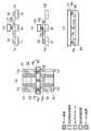
- FIG. 8is a diagram showing a configuration example of a conventional semiconductor device, in which (a) to (c) are layout plan views, (d) is a sectional view taken along line Y81-Y81 ′ in (a), and (e) is ( FIG. 6B is a cross-sectional view taken along line Y82-Y82 ′ of b).
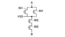
- the configuration of FIG. 8realizes the circuit diagram of FIG.
- two NMOS transistors 901are connected in parallel between the power supply wiring VSS and the terminal A
- two NMOS transistors 902are connected in series between the power supply wiring VSS and the terminal B.
- the two transistors on the upper side of the power supply wiring VSScorrespond to the NMOS transistor 901
- the two transistors on the lower side of the drawingcorrespond to the NMOS transistor 902. .
- FIG. 8Ashows a structure in which a potential is supplied from the power supply wiring VSS installed near the boundary between adjacent transistors to the source region of each transistor through a potential supply wiring and a contact hole.
- a potentialis supplied from the power supply wiring VSS installed near the boundary between adjacent transistors to the source region of each transistor through a potential supply wiring and a contact hole.
- an impurity diffusion region and a contact holeare provided immediately below the power supply wiring VSS, and the power supply wiring VSS is reinforced.
- the potentialis supplied to the source region of each transistor by extracting the source region of each transistor to the position immediately below the power supply wiring VSS provided near the boundary with the adjacent transistor and providing a contact hole. It has a structure. Here, an impurity diffusion region and a contact hole are provided immediately below the power supply wiring VSS, and the power supply wiring VSS is reinforced.
- FIG. 8Cis a modified example of FIG. 8B, in which the impurity diffusion region and the contact hole are provided directly below the power supply wiring VSS only in the portion where the source region of each transistor is extended to the power supply wiring VSS. It has a structure.
- FIGS. 8B and 8CWhen the structure of FIGS. 8B and 8C is used for the structure of FIG. 8A, it is not necessary to use a wiring region from the power supply wiring VSS to the source region of each transistor. Wiring resources that are critical in reducing the cell height of the cell can be effectively used, and this is an effective means for reducing the chip area. That is, the potential supply wiring extending from the source region of the transistor is a metal wiring in FIG. 8A, whereas it is an impurity diffusion region in FIGS. 8B and 8C, and does not use metal wiring resources. Therefore, the area can be reduced.
- FIG. 10Ais a layout structure diagram of the design shape of the impurity diffusion region and the gate electrode forming the source / drain of the transistor. The ends of the gate electrode protruding from the impurity diffusion region are attached to the upper and lower transistors in the drawing. The combined structure is shown.
- FIG. 10Bshows an actual finished shape of the gate electrode with respect to the layout structure of the designed shape shown in FIG.
- OLis the protrusion amount of the gate electrode so that the source region and the drain region do not short-circuit even when the mask misalignment between the gate electrode and the impurity diffusion region occurs
- EXis the thin line pattern receding during gate electrode patterning S is a separation interval for preventing a short circuit between the same layers.
- Lis a length necessary for securing a desired transistor width when the configuration shown in FIGS. 10A and 10B is employed.
- FIGS. 10C and 10Dshow the difference between the design shape and the finished shape when the patterning of the gate electrode is formed by a composite process.
- FIG. 10Cis a layout structure diagram of the design shape of the impurity diffusion region and the gate electrode forming the source / drain of the transistor, and the end portion of the gate electrode protruding from the impurity diffusion region is connected between the upper and lower transistors in the drawing. The structure is shown. Further, a recognition layer 1002 for removing the gate electrode in a later process is provided in a region where the gate electrode of the transistor at the top and bottom of the drawing is connected.
- FIG. 10Dshows the actual finished shape of the gate electrode with respect to the layout structure of the designed shape shown in FIG.
- the gate electrodes of the transistors at the top and bottom of the drawingare separated.
- OLis the protrusion amount of the gate electrode so that the source region and the drain region do not short-circuit even when the mask misalignment between the gate electrode and the impurity diffusion region occurs
- S ′is separated by the gate electrode removal step.
- EXis a thin line pattern retraction amount at the time of gate electrode patterning required in a single process, that is, a margin which is not required in FIG. 10D, and corresponds to a size reduction in the vertical direction of the drawing. .
- the length Lis required in the longitudinal direction of the drawing. Therefore, the length required to form a transistor having the same performance is (L-2 * EX). Thereby, the chip area can be reduced.
- the conventional semiconductor devicehas the following problems.
- FIGS. 11A and 11Bare diagrams showing actual finished shapes of the impurity diffusion regions in the layout configuration shown in FIGS. 8B and 8C described above.
- 1101is the design shape of the opening region of the impurity diffusion region
- 1102is the actual finished shape of the impurity diffusion region.
- Reference numeral 1103denotes a dimensional difference in transistor width between the design shape and the actual finished shape.
- the conventional semiconductor devicehas a problem that the variation in transistor characteristics increases due to the rounding of the impurity diffusion region.
- FIGS. 12A and 12Bshow the case where the gate electrode patterning shown in FIGS. 10C and 10D is formed by a composite process in the layout configuration shown in FIGS. 8B and 8C. It is a figure which shows the actual finishing shape of an impurity diffusion area
- 1201is the design shape of the opening region of the impurity diffusion region
- 1202is the actual finished shape of the impurity diffusion region.
- Reference numeral 1203denotes the separation width of the opening region of the impurity diffusion region in the design shape.
- the isolation width 1203 of the opening region of the impurity diffusion regionis extremely reduced by forming the gate electrode patterning in a composite process, so that the actual finished shape 1202 of the impurity diffusion region is obtained by rounding.
- the shapeis as shown. Therefore, a dimensional difference in transistor width occurs between the design shape 1201 and the actual finished shape 1202, causing a circuit malfunction or a circuit failure due to a short circuit between the source and drain of the transistor. That is, in the conventional semiconductor device, when the patterning of the gate electrode is formed by a composite process, the variation in transistor characteristics due to the rounding of the impurity diffusion region and the processing abnormality of the impurity diffusion region may occur.
- the isolation width 1203 of the opening region of the impurity diffusion regionis set wide, the purpose of reducing the chip area by reducing the layout height is not satisfied.
- an object of the present inventionis to reduce the area of a semiconductor device without causing variations in transistor characteristics and circuit malfunction due to rounding of an impurity diffusion region.
- a semiconductor devicein one embodiment, includes a first impurity diffusion region formed over a substrate and a wiring layer that is above the first impurity diffusion region and extends in a first direction.
- the first local wiringis formed in contact with the upper surface of the first impurity diffusion region and extends below the potential power supply wiring.
- the first local wiring and the potential power supply wiringare electrically connected by the first contact hole. That is, the metal wiring resource is not used for the electrical connection from the impurity diffusion region to the potential power supply wiring, and the local wiring formed in contact with the upper surface of the impurity diffusion region is used. The area can be reduced without being affected by the rounding of the region.
- the local wiringis formed so as to be in contact with the upper surface of the impurity diffusion region, and the structure is drawn out to just below the potential power supply wiring, so that the transistor characteristic variation due to the rounding of the impurity diffusion region can be reduced. Area can be realized.
- FIGS. 1A to 1Care plan views
- FIGS. 2D and 2Eare cross-sectional views
- FIG. 9is a circuit diagram showing a circuit configuration of the semiconductor device of FIGS. 1 to 3 and FIG. 8; It is a figure for demonstrating the characteristic of gate patterning. It is a figure which shows the difference between the design shape in a single process, and a finishing shape. It is a figure which shows the difference between the design shape and finished shape in a composite process.
- FIG. 1A and 1Bare diagrams showing a structure of a semiconductor device according to the first embodiment, wherein FIG. 1A is a layout plan view, FIG. 1B is a cross-sectional view taken along line Ya-Ya ′ in FIG.
- FIG. 6Ais a cross-sectional view taken along line Yb-Yb ′ in FIG. 6A, and
- FIG. 6Dis a cross-sectional view taken along line Xa-Xa ′ in FIG.
- the semiconductor device shown in FIG. 1implements the circuit shown in FIG.
- an impurity diffusion region and a gate electrode constituting a transistorare formed on a substrate (not shown), and a potential feeding wiring and a local wiring for feeding a potential to the transistor are connected by a contact hole.
- the potential supply wiringis shared between the upper and lower transistors in the drawing, and a local wiring is installed directly below the potential power supply wiring through a contact hole, and an impurity diffusion region is in contact directly below the local wiring.
- a three-layer laminated structureis provided.
- the connection between the source region of each transistor and the potential power supply wiringis a structure connected by a local wiring.
- S1is the separation width to the drain composed of the local wiring and the impurity diffusion region constituting the transistor.
- the potential supply wiring 13 extending in the lateral direction (first direction) in the drawingis formed in the wiring layer above the impurity diffusion region.
- the local wiring 12 formed in contact with the upper surface of the impurity diffusion region 11extends below the potential power supply wiring 13, and the potential power supply wiring 13 and the local wiring 12 are electrically connected by a contact hole 14a.
- the local wiring 22 formed in contact with the upper surface of the impurity diffusion region 21also extends below the potential power supply wiring 13, and the potential power supply wiring 13 and the local wiring 22 are electrically connected by a contact hole 14c.
- the local wiring 32 formed in contact with the upper surface of the impurity diffusion region 31also extends below the potential power supply wiring 13.
- the local wirings 12 and 32are integrally formed, and a contact hole for electrically connecting the local wirings 12 and 32 and the potential power supply wiring 13 is shared, and is integrally formed as a contact hole 14a.
- a reinforcing impurity diffusion region 41is formed on the substrate under the potential supply wiring 13, and a reinforcing local wiring 42 is formed in contact with the upper surface of the reinforcing impurity diffusion region 41.
- the potential supply wiring 13 and the reinforcing local wiring 42are electrically connected by contact holes 14a, 14b, and 14c.
- the contact holes 14 a, 14 b, and 14 care arranged on a straight line along the potential supply wiring 13.
- the reinforcing local wiring 42 and the local wirings 12, 22, and 32are integrally formed.
- the minimum value of the isolation width S1is mainly determined by the alignment error, and dimensional variation due to rounding Not affected. For this reason, it can be set sufficiently smaller than the separation interval 1203 of the impurity diffusion layer shown in FIG.
- FIG. 2is a view showing another example of the structure of the semiconductor device according to the present embodiment. 2 also implements the circuit shown in FIG. 9 as in FIG. 1.
- FIG. 2(a) is a layout plan view, and (b) is a cross section taken along line Yc-Yc 'in (a).
- FIG. 4Cis a cross-sectional view taken along line Yd-Yd ′ in FIG. 4A
- FIG. 4Dis a cross-sectional view taken along line Xb-Xb ′ in FIG.
- the configuration in FIG. 2is substantially the same as that in FIG. 1, and the same reference numerals are given to the same components as in FIG. 1, and detailed description thereof is omitted here.
- an impurity diffusion region and a gate electrode constituting a transistorare formed on a substrate (not shown), and a potential feeding wiring and a local wiring for feeding a potential to the transistor are connected by a contact hole.
- the potential supply wiringis shared between the upper and lower transistors in the drawing, and an impurity diffusion region is provided immediately below the potential supply wiring.
- the connection between the source region of each transistor and the impurity diffusion region immediately below the potential power supply wiringis a structure connected by a local wiring, and the structure is connected to the potential power supply wiring through a contact hole on the local wiring.
- S2is the separation width to the drain composed of the impurity diffusion region constituting the local wiring and the transistor.
- FIG. 1is different from FIG. 1 in that no reinforcing local wiring is formed under the potential supply wiring 13. For this reason, even in a region where no local wiring is provided immediately below the potential power supply wiring 13, the potential power supply wiring 13 and the reinforcing impurity diffusion region 41 are directly connected via the contact hole 14 d without passing through the local wiring. . Further, the local wiring 22 formed in contact with the upper surface of the impurity diffusion region 21 extends from below the potential power supply wiring 13 to the empty region.
- the minimum value of the separation width S2is mainly determined by the alignment accuracy, and dimensional variation due to rounding Not affected. For this reason, it can be set sufficiently smaller than the separation interval 1203 of the impurity diffusion layer shown in FIG.
- a local wiring that is not directly connected to the source region of the transistoris provided on the reinforcing impurity diffusion region 41, and a contact hole is provided thereon to connect to the potential power supply wiring 13. Good.
- FIG. 3is a view showing another example of the structure of the semiconductor device according to this embodiment. 3 also implements the circuit shown in FIG. 9 as in FIGS. 1 and 2.
- (a)is a layout plan view
- (b)is a line Ye-Ye in (a).
- (C)is a sectional view taken along line Yf-Yf 'in (a)
- (d)is a sectional view taken along line Xc-Xc' in (a).
- the configuration in FIG. 3is almost the same as that in FIG. 1, and the same reference numerals are given to the same components as in FIG. 1, and detailed description thereof is omitted here.
- an impurity diffusion region and a gate electrode constituting a transistorare formed on a substrate (not shown), and a potential feeding wiring and a local wiring for feeding a potential to the transistor are connected by a contact hole.
- the potential supply wiringis shared between the upper and lower transistors in the drawing, and the connection between the source region of each transistor and the potential supply wiring is connected through a contact hole directly below the potential supply wiring.
- S3is a separation width to the drain composed of the local wiring and the impurity diffusion region constituting the transistor.
- FIG. 1is different from FIG. 1 in that the reinforcing local wiring and the reinforcing impurity diffusion region are not formed under the potential feeding wiring 13. Further, the local wiring 22 formed in contact with the upper surface of the impurity diffusion region 21 extends from below the potential power supply wiring 13 to the empty region.
- the minimum value of the separation width S3is mainly determined by the alignment error, and the size variation due to rounding Not affected. For this reason, it can be set sufficiently smaller than the separation interval 1203 of the impurity diffusion layer shown in FIG.
- the local wiringis formed so as to be in contact with the upper surface of the impurity diffusion region, and the structure is drawn out to a position directly below the potential power supply wiring. Area can be realized.
- FIG. 4is a layout plan view showing the structure of the semiconductor device according to the second embodiment.
- the semiconductor device of FIG. 4is configured by forming each circuit shown in FIG. 5 as a standard cell and arranging these standard cells in an array to constitute a circuit block.
- INVis an inverter circuit cell
- 2NDis a 2-input NAND circuit cell
- 2NRis a 2-input NOR cell
- TAPis a potential feeding cell to a well or a substrate.
- 5Ais an inverter circuit
- FIG. 5Bis a circuit diagram of a 2-input NAND circuit
- FIG. 5Cis a circuit diagram of a 2-input NOR circuit
- 501is a PMOS transistor
- 502is an NMOS transistor.
- the local wiring 401connects the source regions (impurity diffusion regions 411 and 412) of two transistors arranged across the potential power supply wiring VDD in the vertical direction (second direction) of the drawing and the potential power supply wiring VDD. Yes. That is, the local wiring 401 extends from the upper surface of the impurity diffusion region 411 to the upper surface of the impurity diffusion region 412 via the potential supply wiring VDD.
- the local wiring 404extends from the source region (impurity diffusion region 441) of the transistor to the empty region 442 in the adjacent standard cell column across the potential power supply wiring VSS between the standard cell columns.
- the local wirings 406 and 407connect the source regions (impurity diffusion regions 461, 462 or 471, 472) of two transistors adjacent to each other in the left-right direction (first direction) in the drawing and the potential power supply wiring VDD.
- the local wiring 406extends from the upper surface of the impurity diffusion region 461 to the upper surface of the impurity diffusion region 462.
- Reference numeral 402denotes a local wiring for supplying a potential from the potential supply wiring VDD to the well or the substrate.
- Reference numeral 403denotes a local wiring for supplying a potential from the potential supply wiring VSS to the well or the substrate.
- the local wiring 405connects the drains of the NMOS transistor and the PMOS transistor in the standard cell.
- the local wiring 401is shared between the upper and lower standard cells across the potential power supply wiring VDD, and has a structure that can be integrally formed.
- the local wiring 404is shared between the upper and lower standard cells across the potential power supply wiring VSS, and has a structure that can be integrally formed.
- the local wiring 406is shared between the standard cells adjacent to the left and right, and has a structure that can be integrally formed.
- a configurationmay be adopted in which the drains of the NMOS transistor and the PMOS transistor in the standard cell are connected as in the local wiring 405, or via the source region of an adjacent transistor in the horizontal direction in the drawing as in the local wiring 407.
- a configuration in which the power supply wiring VDD and the potential supply wiring VDD are integrally formedmay be employed.
- the structureis such that no reinforcing impurity diffusion region is provided immediately below the potential power supply wiring as shown in FIG. 3, but reinforcement is provided directly below the potential power supply wiring as shown in FIGS.
- a structure having an impurity diffusion region for usemay be used.
- the local wiringis formed so as to be in contact with the upper surface of the impurity diffusion region, and the structure is drawn out to a position directly below the potential power supply wiring.
- the areacan be increased, and the ease of manufacturing the local wiring can be improved.
- FIG. 6A and 6Bare diagrams showing the structure of the semiconductor device according to the third embodiment.
- FIG. 6Ais a layout plan view
- FIG. 6Bis a cross-sectional view taken along line Y1-Y1 ′ in FIG.
- FIG. 7Ais a cross-sectional view taken along line X1-X1 ′
- FIG. 6Dis a cross-sectional view taken along line X2-X2 ′.
- the semiconductor device of FIG. 6implements the AND circuit shown in FIG.
- 701is a PMOS transistor
- 702is an NMOS transistor
- AA and ABare input terminals
- AYis an output terminal.
- connection between the potential supply wirings VDD and VSS and the source region of the transistor, the connection between the potential supply wirings VDD and VSS and the substrate or wellIncludes a configuration in which local wiring is applied to the connection between the drains of the transistors. Further, in the structure of FIG. 6, the local wiring is also connected to the gate electrode.
- reference numeral 601denotes a wiring for connecting the output of the 2-input NAND circuit constituting the AND circuit and the input of the inverter circuit.
- the wiring 601is formed in the same wiring layer as the potential supply wirings VDD and VSS.
- Reference numeral 602denotes a gate electrode
- 603denotes a local wiring formed in contact with the gate electrode 602
- 604denotes a contact hole for electrically connecting the local wiring 603 and the wiring 601.
- the input terminals AA and AB and the inter-element connection wiring 601are connected to the gate electrode through the contact hole and the local wiring.
- the lead-in wiring from the potential supply wirings VDD and VSS to the source region of the transistordoes not interfere with the inter-element connection wiring 601.
- interference between the connection wiring to the input terminals AA and AB and the output terminal AY and the inter-element connection wiring 601can be avoided, so that the area of the standard cell can be reduced.
- the local wiringis formed so as to be in contact with the upper surface of the impurity diffusion region, and the structure is drawn out to a position directly below the potential power supply wiring.
- the areacan be reduced, and further, the area can be further reduced by using the local wiring in combination with the gate electrode.
- the semiconductor device according to the present inventionhas an effect of reducing a margin relating to processing accuracy, alignment, and the like, and is useful for high integration, area reduction, high speed, high reliability, and the like of LSI.
Landscapes
- Engineering & Computer Science (AREA)
- Physics & Mathematics (AREA)
- Condensed Matter Physics & Semiconductors (AREA)
- General Physics & Mathematics (AREA)
- Computer Hardware Design (AREA)
- Microelectronics & Electronic Packaging (AREA)
- Power Engineering (AREA)
- Manufacturing & Machinery (AREA)
- Design And Manufacture Of Integrated Circuits (AREA)
- General Engineering & Computer Science (AREA)
- Metal-Oxide And Bipolar Metal-Oxide Semiconductor Integrated Circuits (AREA)
Abstract
Description
Translated fromJapanese本発明は、半導体装置に関し、特に、高速化及び高集積化を実現する半導体装置に関する。The present invention relates to a semiconductor device, and more particularly to a semiconductor device that realizes high speed and high integration.
従来の半導体装置では、不純物拡散層によって形成されたトランジスタのソース領域をスタンダードセル境界にまで延在させ、スタンダードセル列間で共有する電源配線に接続することによって、スタンダードセル内の配線リソースを確保し、スタンダードセルの面積縮小を実現していた。In the conventional semiconductor device, the source region of the transistor formed by the impurity diffusion layer extends to the standard cell boundary and is connected to the power supply wiring shared between the standard cell columns, thereby securing wiring resources in the standard cell. However, the standard cell area has been reduced.
図8は従来の半導体装置の構成例を示す図であり、(a)~(c)はレイアウト平面図、(d)は(a)の線Y81-Y81’における断面図、(e)は(b)の線Y82-Y82’における断面図である。図8の構成は図9の回路図を実現したものである。図9では、電源配線VSSと端子Aとの間に2個のNMOSトランジスタ901が並列接続されており、また、電源配線VSSと端子Bとの間に2個のNMOSトランジスタ902が直列接続されている。図8(a)~(c)において、電源配線VSSの図面上側にある2個のトランジスタがNMOSトランジスタ901に相当し、図面下側にある2個のトランジスタがNMOSトランジスタ902に相当する。。FIG. 8 is a diagram showing a configuration example of a conventional semiconductor device, in which (a) to (c) are layout plan views, (d) is a sectional view taken along line Y81-Y81 ′ in (a), and (e) is ( FIG. 6B is a cross-sectional view taken along line Y82-Y82 ′ of b). The configuration of FIG. 8 realizes the circuit diagram of FIG. In FIG. 9, two
図8(a)では、隣接するトランジスタとの境界付近に設置された電源配線VSSから電位給電配線およびコンタクトホールを介して、各トランジスタのソース領域に電位が給電される構造となっている。ここで電源配線VSSの直下には、不純物拡散領域及びコンタクトホールが設置されており、電源配線VSSを補強する構造となっている。FIG. 8A shows a structure in which a potential is supplied from the power supply wiring VSS installed near the boundary between adjacent transistors to the source region of each transistor through a potential supply wiring and a contact hole. Here, an impurity diffusion region and a contact hole are provided immediately below the power supply wiring VSS, and the power supply wiring VSS is reinforced.
図8(b)では、隣接するトランジスタとの境界付近に設置された電源配線VSSの直下まで各トランジスタのソース領域を引き出しコンタクトホールを設置することで、各トランジスタのソース領域に電位が給電される構造となっている。ここで、電源配線VSSの直下には、不純物拡散領域及びコンタクトホールが設置されており、電源配線VSSを補強する構造となっている。In FIG. 8B, the potential is supplied to the source region of each transistor by extracting the source region of each transistor to the position immediately below the power supply wiring VSS provided near the boundary with the adjacent transistor and providing a contact hole. It has a structure. Here, an impurity diffusion region and a contact hole are provided immediately below the power supply wiring VSS, and the power supply wiring VSS is reinforced.
図8(c)は、図8(b)の変形例であり、各トランジスタのソース領域が電源配線VSSまで拡張され部分にのみ、電源配線VSSの直下に不純物拡散領域およびコンタクトホールが設置された構造となっている。FIG. 8C is a modified example of FIG. 8B, in which the impurity diffusion region and the contact hole are provided directly below the power supply wiring VSS only in the portion where the source region of each transistor is extended to the power supply wiring VSS. It has a structure.
図8(a)の構造に対して、図8(b)および(c)の構造とした場合には、電源配線VSSから各トランジスタのソース領域までの配線領域を使用する必要がないため、スタンダードセルのセル高さ縮小においてクリティカルとなる配線リソースを有効活用できるので、チップ面積縮小に効果のある手段となる。すなわち、トランジスタのソース領域から延びる電位給電配線が、図8(a)ではメタル配線であるのに対して、図8(b)(c)では不純物拡散領域であり、メタル配線のリソースを使用しないので、面積縮小が可能になる。When the structure of FIGS. 8B and 8C is used for the structure of FIG. 8A, it is not necessary to use a wiring region from the power supply wiring VSS to the source region of each transistor. Wiring resources that are critical in reducing the cell height of the cell can be effectively used, and this is an effective means for reducing the chip area. That is, the potential supply wiring extending from the source region of the transistor is a metal wiring in FIG. 8A, whereas it is an impurity diffusion region in FIGS. 8B and 8C, and does not use metal wiring resources. Therefore, the area can be reduced.
ところで、半導体プロセスの微細化に伴い、ゲート電極のパターニング時の露光工程やエッチング工程を複数回に渡って繰り返し、ゲート電極を精度良く加工する技術が適用され始めている。図10を用いて、ゲート電極のパターニング時に露光工程やエッチング工程を複数回適用する手法(複合工程)による効果について説明する。By the way, with the miniaturization of the semiconductor process, a technique for accurately processing the gate electrode by repeating the exposure process and the etching process at the time of patterning the gate electrode a plurality of times has begun to be applied. The effect of a technique (composite process) in which an exposure process and an etching process are applied multiple times during patterning of the gate electrode will be described with reference to FIG.
図10(a),(b)はゲート電極のパターニングを従来の単一工程で形成した場合の設計形状と仕上がり形状との差を示したものである。図10(a)は、トランジスタのソースドレインを形成する不純物拡散領域とゲート電極の設計形状のレイアウト構造図であり、不純物拡散領域から突き出したゲート電極の端部を、図面上下のトランジスタ同士で付き合わせた構造を示している。10 (a) and 10 (b) show the difference between the design shape and the finished shape when the patterning of the gate electrode is formed by a conventional single process. FIG. 10A is a layout structure diagram of the design shape of the impurity diffusion region and the gate electrode forming the source / drain of the transistor. The ends of the gate electrode protruding from the impurity diffusion region are attached to the upper and lower transistors in the drawing. The combined structure is shown.
図10(b)は、図10(a)の設計形状のレイアウト構造に対する、ゲート電極の実仕上がり形状を示したものである。ここで、OLはゲート電極と不純物拡散領域とのマスク併せズレが発生した場合でも、ソース領域とドレイン領域がショートしないためのゲート電極の突き出し量であり、EXはゲート電極パターニング時の細線パターン後退量であり、Sは同層間でショートさせないための分離間隔である。また、Lは図10(a),(b)のような構成をとった場合の所望のトランジスタ幅を確保するために必要な長さである。FIG. 10B shows an actual finished shape of the gate electrode with respect to the layout structure of the designed shape shown in FIG. Here, OL is the protrusion amount of the gate electrode so that the source region and the drain region do not short-circuit even when the mask misalignment between the gate electrode and the impurity diffusion region occurs, and EX is the thin line pattern receding during gate electrode patterning S is a separation interval for preventing a short circuit between the same layers. L is a length necessary for securing a desired transistor width when the configuration shown in FIGS. 10A and 10B is employed.
一方、図10(c),(d)はゲート電極のパターニングを複合工程で形成した場合の設計形状と仕上がり形状との差を示したものである。図10(c)は、トランジスタのソースドレインを形成する不純物拡散領域とゲート電極の設計形状のレイアウト構造図であり、不純物拡散領域から突き出したゲート電極の端部が、図面上下のトランジスタ同士で接続された構造を示している。また、図面上下のトランジスタのゲート電極が接続された領域には、後工程でゲート電極を除去するための認識層1002が設置されている。On the other hand, FIGS. 10C and 10D show the difference between the design shape and the finished shape when the patterning of the gate electrode is formed by a composite process. FIG. 10C is a layout structure diagram of the design shape of the impurity diffusion region and the gate electrode forming the source / drain of the transistor, and the end portion of the gate electrode protruding from the impurity diffusion region is connected between the upper and lower transistors in the drawing. The structure is shown. Further, a
図10(d)は、図10(c)の設計形状のレイアウト構造に対する、ゲート電極の実仕上がり形状を示したものである。実仕上がり形状では図面上下のトランジスタのゲート電極は分離された構造となっている。ここで、OLはゲート電極と不純物拡散領域とのマスク併せズレが発生した場合でも、ソース領域とドレイン領域がショートしないためのゲート電極の突き出し量であり、S’はゲート電極除去工程によって分離された間隔であり、EXは単一工程で必要とされたゲート電極パターニング時の細線パターン後退量すなわち図10(d)では不要となったマージンであり、図面縦方向での寸法縮小分に相当する。FIG. 10D shows the actual finished shape of the gate electrode with respect to the layout structure of the designed shape shown in FIG. In the actual finished shape, the gate electrodes of the transistors at the top and bottom of the drawing are separated. Here, OL is the protrusion amount of the gate electrode so that the source region and the drain region do not short-circuit even when the mask misalignment between the gate electrode and the impurity diffusion region occurs, and S ′ is separated by the gate electrode removal step. EX is a thin line pattern retraction amount at the time of gate electrode patterning required in a single process, that is, a margin which is not required in FIG. 10D, and corresponds to a size reduction in the vertical direction of the drawing. .
図10に示すように、単一工程でゲート電極のパターニングを行った場合には、図面縦方向において長さがL必要であったものに対して、複合工程でゲート電極のパターニングを行った場合には、同じ性能のトランジスタを形成する場合に必要な長さが(L-2*EX)で済む。これにより、チップ面積を削減することが可能となる。As shown in FIG. 10, when the gate electrode is patterned in a single process, when the gate electrode is patterned in a composite process, the length L is required in the longitudinal direction of the drawing. Therefore, the length required to form a transistor having the same performance is (L-2 * EX). Thereby, the chip area can be reduced.
しかしながら、従来の半導体装置には、以下の課題がある。However, the conventional semiconductor device has the following problems.
図11(a),(b)は、上述の図8(b),(c)で示したレイアウト構成において、不純物拡散領域の実仕上がり形状を示す図である。ここで、1101は不純物拡散領域の開口領域の設計形状であり、1102は不純物拡散領域の実仕上がり形状である。1103は設計形状と実仕上がり形状とのトランジスタ幅の寸法差を示している。FIGS. 11A and 11B are diagrams showing actual finished shapes of the impurity diffusion regions in the layout configuration shown in FIGS. 8B and 8C described above. Here, 1101 is the design shape of the opening region of the impurity diffusion region, and 1102 is the actual finished shape of the impurity diffusion region.
図11に示すように、図8(b),(c)で示したようなトランジスタのソース領域を電源配線直下まで拡張した設計をおこなった場合には、不純物拡散領域の実仕上がり形状1102はラウンディングにより、図示したような形状になる。このため、設計形状1101と実仕上がり形状1102とでトランジスタ幅の寸法差1103が生じ、回路誤動作の原因となる。すなわち、従来の半導体装置では、不純物拡散領域のラウンディングによってトランジスタ特性のばらつきが増大するという問題がある。As shown in FIG. 11, when the transistor source region as shown in FIGS. 8B and 8C is extended to a position just below the power supply wiring, the actual finished
図12(a),(b)は、図8(b),(c)で示したレイアウト構成において、図10(c),(d)で示したゲート電極のパターニングを複合工程で形成した場合の不純物拡散領域の実仕上がり形状を示す図である。ここで、1201は不純物拡散領域の開口領域の設計形状であり、1202は不純物拡散領域の実仕上がり形状である。1203は設計形状における不純物拡散領域の開口領域の分離幅を示している。FIGS. 12A and 12B show the case where the gate electrode patterning shown in FIGS. 10C and 10D is formed by a composite process in the layout configuration shown in FIGS. 8B and 8C. It is a figure which shows the actual finishing shape of an impurity diffusion area | region. Here, 1201 is the design shape of the opening region of the impurity diffusion region, and 1202 is the actual finished shape of the impurity diffusion region.
図12で示すように、ゲート電極のパターニングを複合工程で形成することによって、不純物拡散領域の開口領域の分離幅1203が極端に小さくなるため、不純物拡散領域の実仕上がり形状1202はラウンディングにより、図示したような形状になる。このため、設計形状1201と実仕上がり形状1202とでトランジスタ幅の寸法差が生じ、回路誤動作の原因や、トランジスタのソースとドレインが短絡されたことによる回路不良の原因となる。すなわち、従来の半導体装置では、ゲート電極のパターニングを複合工程で形成した場合に、不純物拡散領域のラウンディングによるトランジスタ特性のばらつき増大や、不純物拡散領域の加工異常が起こりうる。As shown in FIG. 12, the
なお、この問題を回避するために、不純物拡散領域の開口領域の分離幅1203を広く設定した場合には、レイアウト高さ縮小によるチップ面積縮小という目的を満たさなくなる。In order to avoid this problem, when the
前記の問題に鑑み、本発明は、半導体装置において、不純物拡散領域のラウンディングによるトランジスタ特性の変動や回路誤動作を引き起こすことなく、小面積化を実現することを目的とする。In view of the above problems, an object of the present invention is to reduce the area of a semiconductor device without causing variations in transistor characteristics and circuit malfunction due to rounding of an impurity diffusion region.
本発明の一態様では、半導体装置として、基板上に形成された第1の不純物拡散領域と、前記第1の不純物拡散領域より上層にある配線層に形成されており、第1方向に延びる電位給電配線と、前記第1の不純物拡散領域上面に接して形成されており、前記電位給電配線の下まで延びている第1のローカル配線と、前記第1のローカル配線と前記電位給電配線とを電気的に接続する第1のコンタクトホールとを備えたものとする。In one embodiment of the present invention, a semiconductor device includes a first impurity diffusion region formed over a substrate and a wiring layer that is above the first impurity diffusion region and extends in a first direction. A power supply line; a first local line formed in contact with the upper surface of the first impurity diffusion region and extending below the potential power supply line; the first local line and the potential power supply line; A first contact hole that is electrically connected is provided.
この態様によると、第1のローカル配線が、第1の不純物拡散領域上面に接して形成されており、電位給電配線の下まで延びている。そして、第1のコンタクトホールによって、第1のローカル配線と電位給電配線とが電気的に接続されている。すなわち、不純物拡散領域から電位給電配線までの電気的接続のために、メタル配線のリソースが用いられておらず、不純物拡散領域上面に接して形成されたローカル配線が用いられているので、不純物拡散領域のラウンディングの影響を受けることなく、面積縮小が可能になる。According to this aspect, the first local wiring is formed in contact with the upper surface of the first impurity diffusion region and extends below the potential power supply wiring. The first local wiring and the potential power supply wiring are electrically connected by the first contact hole. That is, the metal wiring resource is not used for the electrical connection from the impurity diffusion region to the potential power supply wiring, and the local wiring formed in contact with the upper surface of the impurity diffusion region is used. The area can be reduced without being affected by the rounding of the region.
本発明によれば、不純物拡散領域上面に接するようにローカル配線を形成し、電位給電配線の直下まで引き出す構造とすることによって、不純物拡散領域のラウンディングによるトランジスタ特性変動を発生させること無く、小面積化を実現することができる。According to the present invention, the local wiring is formed so as to be in contact with the upper surface of the impurity diffusion region, and the structure is drawn out to just below the potential power supply wiring, so that the transistor characteristic variation due to the rounding of the impurity diffusion region can be reduced. Area can be realized.
以下、本発明の実施の形態について、図面を参照しながら説明する。Hereinafter, embodiments of the present invention will be described with reference to the drawings.
(第1の実施形態)
図1は第1の実施形態に係る半導体装置の構造を示す図であり、(a)はレイアウト平面図、(b)は(a)の線Ya-Ya’における断面図、(c)は(a)の線Yb-Yb’における断面図、(d)は(a)の線Xa-Xa’における断面図である。図1の半導体装置は図9に示す回路を実現するものである。(First embodiment)
1A and 1B are diagrams showing a structure of a semiconductor device according to the first embodiment, wherein FIG. 1A is a layout plan view, FIG. 1B is a cross-sectional view taken along line Ya-Ya ′ in FIG. FIG. 6A is a cross-sectional view taken along line Yb-Yb ′ in FIG. 6A, and FIG. 6D is a cross-sectional view taken along line Xa-Xa ′ in FIG. The semiconductor device shown in FIG. 1 implements the circuit shown in FIG.
図1の構成では、基板上(図示せず)に、トランジスタを構成する不純物拡散領域およびゲート電極が形成されており、トランジスタに電位を給電するための電位給電配線およびローカル配線がコンタクトホールで接続されている。そして、図面上下のトランジスタ間で電位給電配線を共有する構造となっており、電位給電配線の直下にはコンタクトホールを介してローカル配線が設置され、さらにローカル配線の直下には不純物拡散領域が接するように設置された3層積層構造となっている。各トランジスタのソース領域と電位給電配線との接続は、ローカル配線によって接続される構造となっている。S1は、ローカル配線とトランジスタを構成する不純物拡散領域からなるドレインまでの分離幅である。In the configuration of FIG. 1, an impurity diffusion region and a gate electrode constituting a transistor are formed on a substrate (not shown), and a potential feeding wiring and a local wiring for feeding a potential to the transistor are connected by a contact hole. Has been. The potential supply wiring is shared between the upper and lower transistors in the drawing, and a local wiring is installed directly below the potential power supply wiring through a contact hole, and an impurity diffusion region is in contact directly below the local wiring. A three-layer laminated structure is provided. The connection between the source region of each transistor and the potential power supply wiring is a structure connected by a local wiring. S1 is the separation width to the drain composed of the local wiring and the impurity diffusion region constituting the transistor.
すなわち、不純物拡散領域より上層にある配線層に、図面横方向(第1方向)に延びる電位給電配線13が形成されている。不純物拡散領域11上面に接して形成されたローカル配線12は、電位給電配線13の下まで延びており、電位給電配線13とローカル配線12とはコンタクトホール14aによって電気的に接続されている。また、不純物拡散領域21上面に接して形成されたローカル配線22も電位給電配線13の下まで延びており、電位給電配線13とローカル配線22とはコンタクトホール14cによって電気的に接続されている。さらには、不純物拡散領域31上面に接して形成されたローカル配線32も電位給電配線13の下まで延びている。そして、ローカル配線12,32は一体形成されており、ローカル配線12,32と電位給電配線13とを電気的に接続するコンタクトホールは共通化されており、コンタクトホール14aとして一体形成されている。That is, the
さらには、電位給電配線13の下の基板上に、補強用不純物拡散領域41が形成されており、この補強用不純物拡散領域41上面に接して、補強用ローカル配線42が形成されている。電位給電配線13と補強用ローカル配線42とは、コンタクトホール14a,14b,14cによって電気的に接続されている。コンタクトホール14a,14b,14cは、電位給電配線13に沿って一直線上に配置されている。また、補強用ローカル配線42とローカル配線12,22,32とは、一体に形成されている。Further, a reinforcing
ここで、ローカル配線とトランジスタを構成する不純物拡散領域とは、製造工程上異なる層で形成されるため、分離幅S1の最小値は、主に合わせズレ精度によって決定され、ラウンディングによる寸法変動の影響を受けない。このため、図12(a)で示した不純物拡散層の分離間隔1203よりも十分小さく設定できる。Here, since the local wiring and the impurity diffusion region constituting the transistor are formed in different layers in the manufacturing process, the minimum value of the isolation width S1 is mainly determined by the alignment error, and dimensional variation due to rounding Not affected. For this reason, it can be set sufficiently smaller than the
図2は本実施形態に係る半導体装置の構造の他の例を示す図である。図2の半導体装置も図1と同様に図9に示す回路を実現するものであり、同図中、(a)はレイアウト平面図、(b)は(a)の線Yc-Yc’における断面図、(c)は(a)の線Yd-Yd’における断面図、(d)は(a)は線Xb-Xb’における断面図である。図2の構成は図1とほぼ同様であり、図1と共通の構成要素については同一の符号を付しており、ここではその詳細な説明を省略する。FIG. 2 is a view showing another example of the structure of the semiconductor device according to the present embodiment. 2 also implements the circuit shown in FIG. 9 as in FIG. 1. In FIG. 2, (a) is a layout plan view, and (b) is a cross section taken along line Yc-Yc 'in (a). FIG. 4C is a cross-sectional view taken along line Yd-Yd ′ in FIG. 4A, and FIG. 4D is a cross-sectional view taken along line Xb-Xb ′ in FIG. The configuration in FIG. 2 is substantially the same as that in FIG. 1, and the same reference numerals are given to the same components as in FIG. 1, and detailed description thereof is omitted here.
図2の構成では、基板上(図示せず)に、トランジスタを構成する不純物拡散領域およびゲート電極が形成されており、トランジスタに電位を給電するための電位給電配線およびローカル配線がコンタクトホールで接続されている。そして、図面上下のトランジスタ間で電位給電配線を共有する構造となっており、電位給電配線の直下には不純物拡散領域が設置されている。各トランジスタのソース領域と電位給電配線直下の不純物拡散領域との接続は、ローカル配線によって接続される構造となっており、ローカル配線上のコンタクトホールを介して電位給電配線と接続される構造となっている。S2は、ローカル配線とトランジスタを構成する不純物拡散領域からなるドレインまでの分離幅である。In the configuration of FIG. 2, an impurity diffusion region and a gate electrode constituting a transistor are formed on a substrate (not shown), and a potential feeding wiring and a local wiring for feeding a potential to the transistor are connected by a contact hole. Has been. The potential supply wiring is shared between the upper and lower transistors in the drawing, and an impurity diffusion region is provided immediately below the potential supply wiring. The connection between the source region of each transistor and the impurity diffusion region immediately below the potential power supply wiring is a structure connected by a local wiring, and the structure is connected to the potential power supply wiring through a contact hole on the local wiring. ing. S2 is the separation width to the drain composed of the impurity diffusion region constituting the local wiring and the transistor.
図1と異なっているのは、電位給電配線13の下に、補強用ローカル配線が形成されていない点である。このため、電位給電配線13直下においてローカル配線が設置されていない領域においても、ローカル配線を介すことなく、電位給電配線13と補強用不純物拡散領域41とがコンタクトホール14dで直接接続されている。また、不純物拡散領域21上面に接して形成されたローカル配線22が、電位給電配線13の下からさらに、空き領域まで延びている。1 is different from FIG. 1 in that no reinforcing local wiring is formed under the
ここで、ローカル配線とトランジスタを構成する不純物拡散領域とは、製造工程上異なる層で形成されるため、分離幅S2の最小値は、主に合わせズレ精度によって決定され、ラウンディングによる寸法変動の影響を受けない。このため、図12(a)で示した不純物拡散層の分離間隔1203よりも十分小さく設定できる。Here, since the local wiring and the impurity diffusion region forming the transistor are formed in different layers in the manufacturing process, the minimum value of the separation width S2 is mainly determined by the alignment accuracy, and dimensional variation due to rounding Not affected. For this reason, it can be set sufficiently smaller than the
なお、図2の構成において、補強用不純物拡散領域41上に、トランジスタのソース領域に直接接続されないローカル配線を設置し、その上にコンタクトホールを設置して電位給電配線13と接続する構成としてもよい。In the configuration of FIG. 2, a local wiring that is not directly connected to the source region of the transistor is provided on the reinforcing
図3は本実施形態に係る半導体装置の構造の他の例を示す図である。図3の半導体装置も図1および図2と同様に図9に示す回路を実現するものであり、同図中、(a)はレイアウト平面図、(b)は(a)の線Ye-Ye’における断面図、(c)は(a)の線Yf-Yf’における断面図、(d)は(a)の線Xc-Xc’における断面図である。図3の構成は図1とほぼ同様であり、図1と共通の構成要素については同一の符号を付しており、ここではその詳細な説明を省略する。FIG. 3 is a view showing another example of the structure of the semiconductor device according to this embodiment. 3 also implements the circuit shown in FIG. 9 as in FIGS. 1 and 2. In FIG. 3, (a) is a layout plan view, and (b) is a line Ye-Ye in (a). (C) is a sectional view taken along line Yf-Yf 'in (a), and (d) is a sectional view taken along line Xc-Xc' in (a). The configuration in FIG. 3 is almost the same as that in FIG. 1, and the same reference numerals are given to the same components as in FIG. 1, and detailed description thereof is omitted here.
図3の構成では、基板上(図示せず)に、トランジスタを構成する不純物拡散領域およびゲート電極が形成されており、トランジスタに電位を給電するための電位給電配線およびローカル配線がコンタクトホールで接続されている。そして、図面上下のトランジスタ間で電位給電配線を共有する構造となっており、各トランジスタのソース領域と電位給電配線との接続は、電位給電配線直下のコンタクトホールを介して接続される構造となっている。S3は、ローカル配線とトランジスタを構成する不純物拡散領域からなるドレインまでの分離幅である。In the configuration of FIG. 3, an impurity diffusion region and a gate electrode constituting a transistor are formed on a substrate (not shown), and a potential feeding wiring and a local wiring for feeding a potential to the transistor are connected by a contact hole. Has been. In addition, the potential supply wiring is shared between the upper and lower transistors in the drawing, and the connection between the source region of each transistor and the potential supply wiring is connected through a contact hole directly below the potential supply wiring. ing. S3 is a separation width to the drain composed of the local wiring and the impurity diffusion region constituting the transistor.
図1と異なっているのは、電位給電配線13の下に、補強用ローカル配線および補強用不純物拡散領域が形成されていない点である。また、不純物拡散領域21上面に接して形成されたローカル配線22が、電位給電配線13の下からさらに、空き領域まで延びている。1 is different from FIG. 1 in that the reinforcing local wiring and the reinforcing impurity diffusion region are not formed under the
ここで、ローカル配線とトランジスタを構成する不純物拡散領域とは、製造工程上異なる層で形成されるため、分離幅S3の最小値は、主に合わせズレ精度によって決定され、ラウンディングによる寸法変動の影響を受けない。このため、図12(a)で示した不純物拡散層の分離間隔1203よりも十分小さく設定できる。Here, since the local wiring and the impurity diffusion region constituting the transistor are formed in different layers in the manufacturing process, the minimum value of the separation width S3 is mainly determined by the alignment error, and the size variation due to rounding Not affected. For this reason, it can be set sufficiently smaller than the
本実施形態によると、不純物拡散領域上面に接するようにローカル配線を形成し、電位給電配線の直下まで引き出す構造とすることによって、不純物拡散領域のラウンディングによるトランジスタ特性変動を発生させること無く、小面積化を実現することができる。According to the present embodiment, the local wiring is formed so as to be in contact with the upper surface of the impurity diffusion region, and the structure is drawn out to a position directly below the potential power supply wiring. Area can be realized.
(第2の実施形態)
図4は第2の実施形態に係る半導体装置の構造を示すレイアウト平面図である。図4の半導体装置は、図5に示す各回路をスタンダードセル化し、これらのスタンダードセルをアレイ状に配置することによって回路ブロックを構成したものである。図4において、INVはインバータ回路セル、2NDは2入力NAND回路セル、2NRは2入力NORセル、TAPはウエルまたは基板への電位給電セルである。また図5において、(a)はインバータ回路、(b)は2入力NAND回路、(c)は2入力NOR回路の回路図であり、501はPMOSトランジスタ、502はNMOSトランジスタである。(Second Embodiment)
FIG. 4 is a layout plan view showing the structure of the semiconductor device according to the second embodiment. The semiconductor device of FIG. 4 is configured by forming each circuit shown in FIG. 5 as a standard cell and arranging these standard cells in an array to constitute a circuit block. In FIG. 4, INV is an inverter circuit cell, 2ND is a 2-input NAND circuit cell, 2NR is a 2-input NOR cell, and TAP is a potential feeding cell to a well or a substrate. 5A is an inverter circuit, FIG. 5B is a circuit diagram of a 2-input NAND circuit, FIG. 5C is a circuit diagram of a 2-input NOR circuit, 501 is a PMOS transistor, and 502 is an NMOS transistor.
図4の構造では、第1の実施形態で示したような、不純物拡散領域上面に接しており電位給電配線の直下まで引き出されたローカル配線が、いくつか形成されている。例えば、ローカル配線401は、図面上下方向(第2方向)において電位給電配線VDDを挟んで配置された2つのトランジスタのソース領域(不純物拡散領域411,412)と電位給電配線VDDとを接続している。すなわち、ローカル配線401は、不純物拡散領域411上面から電位給電配線VDDの下を経て、さらに不純物拡散領域412上面まで延びている。ローカル配線404は、トランジスタのソース領域(不純物拡散領域441)からスタンダードセル列間の電位給電配線VSSを跨ぎ隣接するスタンダードセル列内部の空き領域442にまで延在している。ローカル配線406,407は、図面左右方向(第1方向)において隣接する2つのトランジスタのソース領域(不純物拡散領域461,462または471,472)と電位給電配線VDDとを接続している。ローカル配線406は、不純物拡散領域461上面から不純物拡散領域462上面にかけて拡がっている。また、402は電位給電配線VDDからウエル又は基板に電位を給電するためのローカル配線であり、403は電位給電配線VSSからウエル又は基板に電位を給電するためのローカル配線である。ローカル配線405は、スタンダードセル内のNMOSトランジスタとPMOSトランジスタのドレイン間を接続する。In the structure of FIG. 4, as shown in the first embodiment, several local wirings that are in contact with the upper surface of the impurity diffusion region and are drawn out to just below the potential power supply wiring are formed. For example, the
図4に示すように、ローカル配線401は、電位給電配線VDDを挟んだ上下のスタンダードセル間で共有されており、一体形成可能な構造となっている。同様に、ローカル配線404は、電位給電配線VSSを挟んだ上下のスタンダードセル間で共有されており、一体形成可能な構造となっている。また、ローカル配線406は、左右に隣り合うスタンダードセル間で共有されており、一体形成可能な構造となっている。このような構造を採用することによって、ローカル配線の面積を一定以上確保することができ、製造容易性が向上する。As shown in FIG. 4, the
なお、ローカル配線405のようにスタンダードセル内のNMOSトランジスタとPMOSトランジスタのドレイン間を接続する構成としても良いし、ローカル配線407のように、図面左右方向において隣接するトランジスタのソース領域を経由して電位給電配線VDDと接続するように一体形成する構成としてもよい。A configuration may be adopted in which the drains of the NMOS transistor and the PMOS transistor in the standard cell are connected as in the
なお、図4の構造では、図3で示したように電位給電配線の直下に補強用不純物拡散領域を持たない構成としているが、図1また図2で示すような、電位給電配線直下に補強用不純物拡散領域を持つ構成であってもよい。In the structure of FIG. 4, the structure is such that no reinforcing impurity diffusion region is provided immediately below the potential power supply wiring as shown in FIG. 3, but reinforcement is provided directly below the potential power supply wiring as shown in FIGS. A structure having an impurity diffusion region for use may be used.
本実施形態によると、不純物拡散領域上面に接するようにローカル配線を形成し、電位給電配線の直下まで引き出す構造とすることによって、不純物拡散領域のラウンディングによるトランジスタ特性変動を発生させること無く、小面積化を実現することができ、さらに、ローカル配線の製造容易性を向上することができる。According to the present embodiment, the local wiring is formed so as to be in contact with the upper surface of the impurity diffusion region, and the structure is drawn out to a position directly below the potential power supply wiring. The area can be increased, and the ease of manufacturing the local wiring can be improved.
(第3の実施形態)
図6は第3の実施形態に係る半導体装置の構造を示す図であり、(a)はレイアウト平面図、(b)は(a)の線Y1-Y1’における断面図、(c)は(a)の線X1-X1’における断面図、(d)は線X2-X2’における断面図である。図6の半導体装置は図7に示すAND回路を実現するものである。図7において、701はPMOSトランジスタ、702はNMOSトランジスタ、AAおよびABは入力端子、AYは出力端子である。(Third embodiment)
6A and 6B are diagrams showing the structure of the semiconductor device according to the third embodiment. FIG. 6A is a layout plan view, FIG. 6B is a cross-sectional view taken along line Y1-Y1 ′ in FIG. FIG. 7A is a cross-sectional view taken along line X1-X1 ′, and FIG. 6D is a cross-sectional view taken along line X2-X2 ′. The semiconductor device of FIG. 6 implements the AND circuit shown in FIG. In FIG. 7, 701 is a PMOS transistor, 702 is an NMOS transistor, AA and AB are input terminals, and AY is an output terminal.
図6の構造では、第1および第2の実施形態で示したような、電位給電配線VDD,VSSとトランジスタのソース領域との接続、電位給電配線VDD,VSSと基板またはウエルとの接続、さらには、トランジスタのドレイン間の接続に対してローカル配線を適用する構成が、含まれている。さらに図6の構造では、ゲート電極に対してもローカル配線を接続する構成としている。In the structure of FIG. 6, as shown in the first and second embodiments, the connection between the potential supply wirings VDD and VSS and the source region of the transistor, the connection between the potential supply wirings VDD and VSS and the substrate or well, Includes a configuration in which local wiring is applied to the connection between the drains of the transistors. Further, in the structure of FIG. 6, the local wiring is also connected to the gate electrode.
図6において、601はAND回路を構成する2入力NAND回路の出力とインバータ回路の入力とを接続する配線である。配線601は電位給電配線VDD,VSSと同じ配線層に形成されている。602はゲート電極、603はゲート電極602に接して形成されたローカル配線、604はローカル配線603と配線601とを電気的に接続するコンタクトホールである。In FIG. 6,
図6(d)に示すように、入力端子AA,ABおよび素子間接続配線601は、コンタクトホールおよびローカル配線を介してゲート電極と接続されている。これにより、スタンダードセルの高さ(図面上下方向)を低く設定した場合でも、電位給電配線VDD,VSSからトランジスタのソース領域までの引き込み配線が、素子間接続配線601と干渉することがない。このため、入力端子AA,ABや出力端子AYへの接続配線と素子間接続配線601との干渉を回避することができるので、スタンダードセルの面積を縮小することができる。As shown in FIG. 6D, the input terminals AA and AB and the
本実施形態によると、不純物拡散領域上面に接するようにローカル配線を形成し、電位給電配線の直下まで引き出す構造とすることによって、不純物拡散領域のラウンディングによるトランジスタ特性変動を発生させること無く、小面積化を実現することができ、さらに、ローカル配線をゲート電極にも併用することによって、更なる小面積化を実現することができる。According to the present embodiment, the local wiring is formed so as to be in contact with the upper surface of the impurity diffusion region, and the structure is drawn out to a position directly below the potential power supply wiring. The area can be reduced, and further, the area can be further reduced by using the local wiring in combination with the gate electrode.
本発明に係る半導体装置は、加工精度及び位置合わせ等に関するマージンを削減する効果を有し、LSI等の高集積化、面積縮小、高速化及び高信頼性化等のために有用である。The semiconductor device according to the present invention has an effect of reducing a margin relating to processing accuracy, alignment, and the like, and is useful for high integration, area reduction, high speed, high reliability, and the like of LSI.
11,21,31 不純物拡散領域
12,22,32 ローカル配線
13 電位給電配線
14a,14b,14c,14d コンタクトホール
41 補強用不純物拡散領域
42 補強用ローカル配線
401,404,406,407 ローカル配線
411,412,441,461,462,471,472 不純物拡散領域
442 空き領域
601 配線
602 ゲート電極
603 ローカル配線
604 コンタクトホール11, 21, 31
Claims (10)
Translated fromJapanese前記第1の不純物拡散領域より上層にある配線層に形成されており、第1方向に延びる電位給電配線と、
前記第1の不純物拡散領域上面に接して形成されており、前記電位給電配線の下まで延びている第1のローカル配線と、
前記第1のローカル配線と前記電位給電配線とを電気的に接続する第1のコンタクトホールとを備えた
ことを特徴とする半導体装置。A first impurity diffusion region formed on the substrate;
A potential supply wiring formed in a wiring layer above the first impurity diffusion region and extending in a first direction;
A first local wiring formed in contact with the upper surface of the first impurity diffusion region and extending under the potential power supply wiring;
A semiconductor device comprising: a first contact hole that electrically connects the first local wiring and the potential power supply wiring.
前記基板上に形成された第2の不純物拡散領域と、
前記第2の不純物拡散領域上面に接して形成されており、前記電位給電配線の下まで延びている第2のローカル配線と、
前記第2のローカル配線と前記電位給電配線とを電気的に接続する第2のコンタクトホールとを備えた
ことを特徴とする半導体装置。The semiconductor device according to claim 1,
A second impurity diffusion region formed on the substrate;
A second local wiring formed in contact with the upper surface of the second impurity diffusion region and extending under the potential power supply wiring;
A semiconductor device comprising: a second contact hole for electrically connecting the second local wiring and the potential power supply wiring.
前記第1および第2のコンタクトホールは、前記電位給電配線に沿って一直線上に配置されている
ことを特徴とする半導体装置。The semiconductor device according to claim 2,
The semiconductor device according to claim 1, wherein the first and second contact holes are arranged in a straight line along the potential supply wiring.
前記第1および第2のローカル配線は、一体形成されており、
前記第1および第2のコンタクトホールは、共通化され一体形成されている
ことを特徴とする半導体装置。The semiconductor device according to claim 2, wherein the first and second local wirings are integrally formed,
The semiconductor device according to claim 1, wherein the first and second contact holes are shared and integrally formed.
前記電位給電配線の下の基板上に形成された、補強用不純物拡散領域と、
前記補強用不純物拡散領域上面に接して形成されており、前記電位給電配線とコンタクトホールを介して電気的に接続された補強用ローカル配線とを備え、
前記補強用ローカル配線は、前記第1のローカル配線と、一体に形成されている
ことを特徴とする半導体装置。The semiconductor device according to claim 1,
A reinforcing impurity diffusion region formed on the substrate under the potential power supply wiring; and
It is formed in contact with the upper surface of the reinforcing impurity diffusion region, and includes a reinforcing local wiring electrically connected to the potential power supply wiring through a contact hole,
The semiconductor device according to claim 1, wherein the reinforcing local wiring is formed integrally with the first local wiring.
前記電位給電配線の下の基板上に形成されており、前記電位給電配線とコンタクトホールを介して電気的に接続された補強用不純物拡散領域を備えている
ことを特徴とする半導体装置。The semiconductor device according to claim 1,
A semiconductor device comprising a reinforcing impurity diffusion region formed on a substrate under the potential power supply wiring and electrically connected to the potential power supply wiring through a contact hole.
前記基板上に形成されており、前記第1方向と直交する方向である第2方向において、前記電位給電配線を挟んで前記第1の不純物拡散領域と隣り合う第2の不純物拡散領域を備え、
前記第1のローカル配線は、前記電位給電配線の下からさらに、前記第2の不純物拡散領域上面にかけて延びており、かつ、前記第2の不純物拡散領域上面に接して形成されている
ことを特徴とする半導体装置。The semiconductor device according to claim 1,
A second impurity diffusion region that is formed on the substrate and is adjacent to the first impurity diffusion region across the potential supply wiring in a second direction that is perpendicular to the first direction;
The first local wiring extends from below the potential power supply wiring to an upper surface of the second impurity diffusion region, and is formed in contact with the upper surface of the second impurity diffusion region. A semiconductor device.
前記第1方向と直交する方向である第2方向において、前記電位給電配線を挟んで前記第1の不純物拡散領域と隣り合う空き領域を備え、
前記第1のローカル配線は、前記電位給電配線の下からさらに、前記空き領域まで延びている
ことを特徴とする半導体装置。The semiconductor device according to claim 1,
In a second direction, which is a direction orthogonal to the first direction, includes a vacant region adjacent to the first impurity diffusion region across the potential supply wiring,
The semiconductor device according to claim 1, wherein the first local wiring further extends from under the potential power supply wiring to the empty area.
前記基板上に形成されており、前記第1の不純物拡散領域と前記第1方向において隣り合う第2の不純物拡散領域を備え、
前記第1のローカル配線は、前記第1の不純物拡散領域上面から前記第2の不純物拡散領域上面にかけて拡がっており、かつ、前記第2の不純物拡散領域上面に接して形成されている
ことを特徴とする半導体装置。The semiconductor device according to claim 1,
A second impurity diffusion region formed on the substrate and adjacent to the first impurity diffusion region in the first direction;
The first local wiring extends from the upper surface of the first impurity diffusion region to the upper surface of the second impurity diffusion region, and is formed in contact with the upper surface of the second impurity diffusion region. A semiconductor device.
ゲート電極と、
前記配線層に形成された配線と、
前記ゲート電極に接して形成された第2のローカル配線と、
前記第2のローカル配線と前記配線とを電気的に接続する第2のコンタクトホールとを備えた
ことを特徴とする半導体装置。The semiconductor device according to claim 1,
A gate electrode;
Wiring formed in the wiring layer;
A second local wiring formed in contact with the gate electrode;
A semiconductor device comprising: the second local wiring and a second contact hole for electrically connecting the wiring.
Priority Applications (5)
| Application Number | Priority Date | Filing Date | Title |
|---|---|---|---|
| CN2011800218129ACN102870207A (en) | 2010-10-26 | 2011-07-22 | Semiconductor device |
| US13/659,229US9099447B2 (en) | 2010-10-26 | 2012-10-24 | Semiconductor device |
| US14/754,174US9412757B2 (en) | 2010-10-26 | 2015-06-29 | Semiconductor device |
| US15/204,723US9831271B2 (en) | 2010-10-26 | 2016-07-07 | Semiconductor device |
| US15/796,329US10403644B2 (en) | 2010-10-26 | 2017-10-27 | Semiconductor device |
Applications Claiming Priority (2)
| Application Number | Priority Date | Filing Date | Title |
|---|---|---|---|
| JP2010239997 | 2010-10-26 | ||
| JP2010-239997 | 2010-10-26 |
Related Child Applications (1)
| Application Number | Title | Priority Date | Filing Date |
|---|---|---|---|
| US13/659,229ContinuationUS9099447B2 (en) | 2010-10-26 | 2012-10-24 | Semiconductor device |
Publications (1)
| Publication Number | Publication Date |
|---|---|
| WO2012056615A1true WO2012056615A1 (en) | 2012-05-03 |
Family
ID=45993364
Family Applications (1)
| Application Number | Title | Priority Date | Filing Date |
|---|---|---|---|
| PCT/JP2011/004147WO2012056615A1 (en) | 2010-10-26 | 2011-07-22 | Semiconductor device |
Country Status (3)
| Country | Link |
|---|---|
| US (4) | US9099447B2 (en) |
| CN (1) | CN102870207A (en) |
| WO (1) | WO2012056615A1 (en) |
Cited By (1)
| Publication number | Priority date | Publication date | Assignee | Title |
|---|---|---|---|---|
| WO2013161249A1 (en)* | 2012-04-24 | 2013-10-31 | パナソニック株式会社 | Semiconductor device |
Families Citing this family (26)
| Publication number | Priority date | Publication date | Assignee | Title |
|---|---|---|---|---|
| USRE46672E1 (en) | 2006-07-13 | 2018-01-16 | Velodyne Lidar, Inc. | High definition LiDAR system |
| US9831230B2 (en)* | 2013-08-13 | 2017-11-28 | Taiwan Semiconductor Manufacturing Company, Ltd. | Standard cell layout, semiconductor device having engineering change order (ECO) cells and method |
| US9653346B2 (en) | 2015-05-07 | 2017-05-16 | United Microelectronics Corp. | Integrated FinFET structure having a contact plug pitch larger than fin and first metal pitch |
| US9673145B2 (en)* | 2015-05-07 | 2017-06-06 | United Microelectronics Corp. | Semiconductor integrated circuit layout structure |
| US9793211B2 (en) | 2015-10-20 | 2017-10-17 | Taiwan Semiconductor Manufacturing Co., Ltd. | Dual power structure with connection pins |
| US10510688B2 (en)* | 2015-10-26 | 2019-12-17 | Taiwan Semiconductor Manufacturing Co., Ltd. | Via rail solution for high power electromigration |
| US9570395B1 (en)* | 2015-11-17 | 2017-02-14 | Samsung Electronics Co., Ltd. | Semiconductor device having buried power rail |
| US10627490B2 (en) | 2016-01-31 | 2020-04-21 | Velodyne Lidar, Inc. | Multiple pulse, LIDAR based 3-D imaging |
| EP3430428B1 (en) | 2016-03-19 | 2025-04-02 | Velodyne Lidar USA, Inc. | Integrated illumination and detection for lidar based 3-d imaging |
| WO2017210418A1 (en) | 2016-06-01 | 2017-12-07 | Velodyne Lidar, Inc. | Multiple pixel scanning lidar |
| US9960231B2 (en)* | 2016-06-17 | 2018-05-01 | Qualcomm Incorporated | Standard cell architecture for parasitic resistance reduction |
| CN115172453A (en)* | 2016-08-08 | 2022-10-11 | 联华电子股份有限公司 | Semiconductor device with a plurality of transistors |
| EP3593166B1 (en) | 2017-03-31 | 2024-04-17 | Velodyne Lidar USA, Inc. | Integrated lidar illumination power control |
| CN110809704B (en) | 2017-05-08 | 2022-11-01 | 威力登激光雷达美国有限公司 | LIDAR data acquisition and control |
| US10692808B2 (en) | 2017-09-18 | 2020-06-23 | Qualcomm Incorporated | High performance cell design in a technology with high density metal routing |
| US11294041B2 (en)* | 2017-12-08 | 2022-04-05 | Velodyne Lidar Usa, Inc. | Systems and methods for improving detection of a return signal in a light ranging and detection system |
| US10756114B2 (en) | 2017-12-28 | 2020-08-25 | Taiwan Semiconductor Manufacturing Co., Ltd. | Semiconductor circuit with metal structure and manufacturing method |
| US11971507B2 (en) | 2018-08-24 | 2024-04-30 | Velodyne Lidar Usa, Inc. | Systems and methods for mitigating optical crosstalk in a light ranging and detection system |
| US10712434B2 (en) | 2018-09-18 | 2020-07-14 | Velodyne Lidar, Inc. | Multi-channel LIDAR illumination driver |
| US10483200B1 (en) | 2018-09-27 | 2019-11-19 | Qualcomm Incorporated | Integrated circuits (ICs) employing additional output vertical interconnect access(es) (VIA(s)) coupled to a circuit output VIA to decrease circuit output resistance |
| US11562953B2 (en) | 2018-10-23 | 2023-01-24 | Taiwan Semiconductor Manufacturing Company, Ltd. | Cell having stacked pick-up region |
| US11082010B2 (en) | 2018-11-06 | 2021-08-03 | Velodyne Lidar Usa, Inc. | Systems and methods for TIA base current detection and compensation |
| US12061263B2 (en) | 2019-01-07 | 2024-08-13 | Velodyne Lidar Usa, Inc. | Systems and methods for a configurable sensor system |
| US11885958B2 (en) | 2019-01-07 | 2024-01-30 | Velodyne Lidar Usa, Inc. | Systems and methods for a dual axis resonant scanning mirror |
| US10613203B1 (en) | 2019-07-01 | 2020-04-07 | Velodyne Lidar, Inc. | Interference mitigation for light detection and ranging |
| KR20220085138A (en) | 2020-12-15 | 2022-06-22 | 삼성전자주식회사 | Semiconductor device, layout design method for the same and method for fabricating the same |
Citations (9)
| Publication number | Priority date | Publication date | Assignee | Title |
|---|---|---|---|---|
| JPS58116760A (en)* | 1981-12-29 | 1983-07-12 | Fujitsu Ltd | Complementary MOS semiconductor device |
| JPS58202553A (en)* | 1982-05-21 | 1983-11-25 | Toshiba Corp | Semiconductor device |
| JPH01133342A (en)* | 1987-11-18 | 1989-05-25 | Matsushita Electron Corp | Semiconductor integrated circuit |
| JPH0567738A (en)* | 1991-09-09 | 1993-03-19 | Hitachi Ltd | Semiconductor integrated circuit device |
| JPH0594968A (en)* | 1991-05-10 | 1993-04-16 | Toshiba Corp | Semiconductor device and manufacturing method thereof |
| JP2000031286A (en)* | 1998-07-14 | 2000-01-28 | Nec Corp | Semiconductor integrated circuit device |
| JP2003197768A (en)* | 2001-12-25 | 2003-07-11 | Toshiba Corp | Semiconductor device and manufacturing method thereof |
| JP2007043004A (en)* | 2005-08-05 | 2007-02-15 | Nec Electronics Corp | Semiconductor integrated circuit device |
| JP2009032788A (en)* | 2007-07-25 | 2009-02-12 | Renesas Technology Corp | Semiconductor device |
Family Cites Families (15)
| Publication number | Priority date | Publication date | Assignee | Title |
|---|---|---|---|---|
| US5355023A (en)* | 1992-06-05 | 1994-10-11 | Nippon Steel Corporation | Semiconductor device having conducting layers connected through contact holes |
| JPH08250600A (en)* | 1995-03-08 | 1996-09-27 | Matsushita Electric Ind Co Ltd | Semiconductor device and manufacturing method thereof |
| US6617621B1 (en)* | 2000-06-06 | 2003-09-09 | Virage Logic Corporation | Gate array architecture using elevated metal levels for customization |
| JP2005116969A (en)* | 2003-10-10 | 2005-04-28 | Toshiba Corp | Semiconductor device and manufacturing method thereof |
| JP2005159131A (en)* | 2003-11-27 | 2005-06-16 | Nec Electronics Corp | Semiconductor memory device and manufacturing method thereof |
| US7323752B2 (en)* | 2004-09-30 | 2008-01-29 | Taiwan Semiconductor Manufacturing Co., Ltd. | ESD protection circuit with floating diffusion regions |
| JP2006228954A (en)* | 2005-02-17 | 2006-08-31 | Matsushita Electric Ind Co Ltd | Semiconductor device and layout design method thereof |
| JP4827422B2 (en)* | 2005-03-10 | 2011-11-30 | ルネサスエレクトロニクス株式会社 | Semiconductor integrated circuit device design method, apparatus and program |
| JP2007103607A (en)* | 2005-10-03 | 2007-04-19 | Matsushita Electric Ind Co Ltd | Standard cell, semiconductor integrated circuit, semiconductor integrated circuit design method, semiconductor integrated circuit design apparatus, and standard cell library |
| US7446352B2 (en)* | 2006-03-09 | 2008-11-04 | Tela Innovations, Inc. | Dynamic array architecture |
| JP4882455B2 (en)* | 2006-03-31 | 2012-02-22 | 富士通セミコンダクター株式会社 | Unit cell of semiconductor integrated circuit, wiring method using unit cell, and wiring program |
| JP2008004790A (en) | 2006-06-23 | 2008-01-10 | Oki Electric Ind Co Ltd | Standard cell |
| US8063415B2 (en)* | 2007-07-25 | 2011-11-22 | Renesas Electronics Corporation | Semiconductor device |
| US8504972B2 (en)* | 2009-04-15 | 2013-08-06 | Taiwan Semiconductor Manufacturing Company, Ltd. | Standard cells having flexible layout architecture/boundaries |
| US8507957B2 (en)* | 2011-05-02 | 2013-08-13 | Taiwan Semiconductor Manufacturing Company, Ltd. | Integrated circuit layouts with power rails under bottom metal layer |
- 2011
- 2011-07-22WOPCT/JP2011/004147patent/WO2012056615A1/enactiveApplication Filing
- 2011-07-22CNCN2011800218129Apatent/CN102870207A/enactivePending
- 2012
- 2012-10-24USUS13/659,229patent/US9099447B2/enactiveActive
- 2015
- 2015-06-29USUS14/754,174patent/US9412757B2/enactiveActive
- 2016
- 2016-07-07USUS15/204,723patent/US9831271B2/enactiveActive
- 2017
- 2017-10-27USUS15/796,329patent/US10403644B2/enactiveActive
Patent Citations (9)
| Publication number | Priority date | Publication date | Assignee | Title |
|---|---|---|---|---|
| JPS58116760A (en)* | 1981-12-29 | 1983-07-12 | Fujitsu Ltd | Complementary MOS semiconductor device |
| JPS58202553A (en)* | 1982-05-21 | 1983-11-25 | Toshiba Corp | Semiconductor device |
| JPH01133342A (en)* | 1987-11-18 | 1989-05-25 | Matsushita Electron Corp | Semiconductor integrated circuit |
| JPH0594968A (en)* | 1991-05-10 | 1993-04-16 | Toshiba Corp | Semiconductor device and manufacturing method thereof |
| JPH0567738A (en)* | 1991-09-09 | 1993-03-19 | Hitachi Ltd | Semiconductor integrated circuit device |
| JP2000031286A (en)* | 1998-07-14 | 2000-01-28 | Nec Corp | Semiconductor integrated circuit device |
| JP2003197768A (en)* | 2001-12-25 | 2003-07-11 | Toshiba Corp | Semiconductor device and manufacturing method thereof |
| JP2007043004A (en)* | 2005-08-05 | 2007-02-15 | Nec Electronics Corp | Semiconductor integrated circuit device |
| JP2009032788A (en)* | 2007-07-25 | 2009-02-12 | Renesas Technology Corp | Semiconductor device |
Cited By (2)
| Publication number | Priority date | Publication date | Assignee | Title |
|---|---|---|---|---|
| WO2013161249A1 (en)* | 2012-04-24 | 2013-10-31 | パナソニック株式会社 | Semiconductor device |
| US9343461B2 (en) | 2012-04-24 | 2016-05-17 | Socionext Inc. | Semiconductor device including a local wiring connecting diffusion regions |
Also Published As
| Publication number | Publication date |
|---|---|
| CN102870207A (en) | 2013-01-09 |
| US9412757B2 (en) | 2016-08-09 |
| US20180053783A1 (en) | 2018-02-22 |
| US9831271B2 (en) | 2017-11-28 |
| US20150303216A1 (en) | 2015-10-22 |
| US9099447B2 (en) | 2015-08-04 |
| US20160322383A1 (en) | 2016-11-03 |
| US20130113112A1 (en) | 2013-05-09 |
| US10403644B2 (en) | 2019-09-03 |
Similar Documents
| Publication | Publication Date | Title |
|---|---|---|
| WO2012056615A1 (en) | Semiconductor device | |
| TWI599019B (en) | An integrated circuit including a cross-coupled transistor configuration in a logic gate layout layout, a method for generating the layout thereof, and a data storage device including instructions for generating a layout thereof | |
| JP5230251B2 (en) | Standard cell layout structure, standard cell library, and semiconductor integrated circuit layout structure | |
| US20080180132A1 (en) | Semiconductor device and method of fabricating the same | |
| US20090020784A1 (en) | Method for designing semiconductor device and semiconductor device | |
| JPWO2018042986A1 (en) | Semiconductor integrated circuit device | |
| CN113196463A (en) | Semiconductor integrated circuit device having a plurality of semiconductor chips | |
| CN113196464A (en) | Semiconductor integrated circuit device having a plurality of semiconductor chips | |
| JP5547934B2 (en) | Semiconductor device, semiconductor device manufacturing method, and semiconductor device layout method | |
| US20090127721A1 (en) | Semiconductor integrated circuit device | |
| CN110392922B (en) | Semiconductor integrated circuit device with a plurality of semiconductor chips | |
| JP2010003953A (en) | Semiconductor integrated circuit | |
| US7501710B2 (en) | Semiconductor integrated circuit and method of manufacturing the same | |
| JP2011199034A (en) | Semiconductor device | |
| JP5168872B2 (en) | Semiconductor integrated circuit | |
| WO2013161249A1 (en) | Semiconductor device | |
| JP5592560B2 (en) | Semiconductor device and manufacturing method of semiconductor device | |
| JP2010010590A (en) | Semiconductor device and its manufacturing method | |
| JP5021891B2 (en) | Semiconductor integrated circuit pattern generation method, semiconductor integrated circuit, and manufacturing method thereof | |
| JP7323847B2 (en) | Semiconductor integrated circuit device | |
| JP5711812B2 (en) | Semiconductor device | |
| JP2005353683A (en) | Semiconductor integrated circuit | |
| JP2011003779A (en) | Semiconductor integrated circuit device | |
| JP2008270827A (en) | Semiconductor device |
Legal Events
| Date | Code | Title | Description |
|---|---|---|---|
| WWE | Wipo information: entry into national phase | Ref document number:201180021812.9 Country of ref document:CN | |
| 121 | Ep: the epo has been informed by wipo that ep was designated in this application | Ref document number:11835763 Country of ref document:EP Kind code of ref document:A1 | |
| NENP | Non-entry into the national phase | Ref country code:DE | |
| 122 | Ep: pct application non-entry in european phase | Ref document number:11835763 Country of ref document:EP Kind code of ref document:A1 | |
| NENP | Non-entry into the national phase | Ref country code:JP |