WO2012046319A1 - Solar cell module, photovoltaic device, and process for manufacture of solar cell module - Google Patents
Solar cell module, photovoltaic device, and process for manufacture of solar cell moduleDownload PDFInfo
- Publication number
- WO2012046319A1 WO2012046319A1PCT/JP2010/067591JP2010067591WWO2012046319A1WO 2012046319 A1WO2012046319 A1WO 2012046319A1JP 2010067591 WJP2010067591 WJP 2010067591WWO 2012046319 A1WO2012046319 A1WO 2012046319A1
- Authority
- WO
- WIPO (PCT)
- Prior art keywords
- light
- solar cell
- cell module
- oxide
- wavelength range
- Prior art date
Links
- 238000004519manufacturing processMethods0.000titleclaimsdescription31
- 238000000034methodMethods0.000titleclaimsdescription29
- 238000007789sealingMethods0.000claimsabstractdescription124
- 239000000758substrateSubstances0.000claimsabstractdescription65
- 238000000149argon plasma sinteringMethods0.000claimsabstractdescription59
- 239000000463materialSubstances0.000claimsabstractdescription56
- 229910052751metalInorganic materials0.000claimsabstractdescription42
- 239000002184metalSubstances0.000claimsabstractdescription42
- 238000010521absorption reactionMethods0.000claimsabstractdescription35
- 230000001681protective effectEffects0.000claimsabstractdescription31
- GWEVSGVZZGPLCZ-UHFFFAOYSA-NTitan oxideChemical compoundO=[Ti]=OGWEVSGVZZGPLCZ-UHFFFAOYSA-N0.000claimsdescription30
- 239000002245particleSubstances0.000claimsdescription23
- 229910052782aluminiumInorganic materials0.000claimsdescription22
- XAGFODPZIPBFFR-UHFFFAOYSA-NaluminiumChemical compound[Al]XAGFODPZIPBFFR-UHFFFAOYSA-N0.000claimsdescription22
- UQSXHKLRYXJYBZ-UHFFFAOYSA-NIron oxideChemical compound[Fe]=OUQSXHKLRYXJYBZ-UHFFFAOYSA-N0.000claimsdescription20
- 239000000126substanceSubstances0.000claimsdescription14
- 239000004408titanium dioxideSubstances0.000claimsdescription14
- UCKMPCXJQFINFW-UHFFFAOYSA-NSulphideChemical compound[S-2]UCKMPCXJQFINFW-UHFFFAOYSA-N0.000claimsdescription13
- RYGMFSIKBFXOCR-UHFFFAOYSA-NCopperChemical compound[Cu]RYGMFSIKBFXOCR-UHFFFAOYSA-N0.000claimsdescription10
- 229910000502Li-aluminosilicateInorganic materials0.000claimsdescription10
- PWHULOQIROXLJO-UHFFFAOYSA-NManganeseChemical compound[Mn]PWHULOQIROXLJO-UHFFFAOYSA-N0.000claimsdescription10
- 229910000503Na-aluminosilicateInorganic materials0.000claimsdescription10
- PXHVJJICTQNCMI-UHFFFAOYSA-NNickelChemical compound[Ni]PXHVJJICTQNCMI-UHFFFAOYSA-N0.000claimsdescription10
- JGDFBJMWFLXCLJ-UHFFFAOYSA-Ncopper chromiteChemical compound[Cu]=O.[Cu]=O.O=[Cr]O[Cr]=OJGDFBJMWFLXCLJ-UHFFFAOYSA-N0.000claimsdescription10
- 229910052748manganeseInorganic materials0.000claimsdescription10
- 239000011572manganeseSubstances0.000claimsdescription10
- NUJOXMJBOLGQSY-UHFFFAOYSA-Nmanganese dioxideChemical compoundO=[Mn]=ONUJOXMJBOLGQSY-UHFFFAOYSA-N0.000claimsdescription10
- 230000003287optical effectEffects0.000claimsdescription10
- 239000003566sealing materialSubstances0.000claimsdescription10
- 239000000429sodium aluminium silicateSubstances0.000claimsdescription10
- 235000012217sodium aluminium silicateNutrition0.000claimsdescription10
- URGAHOPLAPQHLN-UHFFFAOYSA-Nsodium aluminosilicateChemical compound[Na+].[Al+3].[O-][Si]([O-])=O.[O-][Si]([O-])=OURGAHOPLAPQHLN-UHFFFAOYSA-N0.000claimsdescription10
- SXQXMCWCWVCFPC-UHFFFAOYSA-Naluminum;potassium;dioxido(oxo)silaneChemical compound[Al+3].[K+].[O-][Si]([O-])=O.[O-][Si]([O-])=OSXQXMCWCWVCFPC-UHFFFAOYSA-N0.000claimsdescription9
- 229910052709silverInorganic materials0.000claimsdescription9
- 239000004332silverSubstances0.000claimsdescription9
- RTAQQCXQSZGOHL-UHFFFAOYSA-NTitaniumChemical compound[Ti]RTAQQCXQSZGOHL-UHFFFAOYSA-N0.000claimsdescription8
- 239000010936titaniumSubstances0.000claimsdescription8
- 229910052719titaniumInorganic materials0.000claimsdescription8
- 238000001579optical reflectometryMethods0.000claimsdescription7
- WUPHOULIZUERAE-UHFFFAOYSA-N3-(oxolan-2-yl)propanoic acidChemical compoundOC(=O)CCC1CCCO1WUPHOULIZUERAE-UHFFFAOYSA-N0.000claimsdescription5
- QPLDLSVMHZLSFG-UHFFFAOYSA-NCopper oxideChemical compound[Cu]=OQPLDLSVMHZLSFG-UHFFFAOYSA-N0.000claimsdescription5
- 239000005751Copper oxideSubstances0.000claimsdescription5
- BQCADISMDOOEFD-UHFFFAOYSA-NSilverChemical compound[Ag]BQCADISMDOOEFD-UHFFFAOYSA-N0.000claimsdescription5
- ATJFFYVFTNAWJD-UHFFFAOYSA-NTinChemical compound[Sn]ATJFFYVFTNAWJD-UHFFFAOYSA-N0.000claimsdescription5
- WGLPBDUCMAPZCE-UHFFFAOYSA-NTrioxochromiumChemical compoundO=[Cr](=O)=OWGLPBDUCMAPZCE-UHFFFAOYSA-N0.000claimsdescription5
- HCHKCACWOHOZIP-UHFFFAOYSA-NZincChemical compound[Zn]HCHKCACWOHOZIP-UHFFFAOYSA-N0.000claimsdescription5
- JYDZYJYYCYREGF-UHFFFAOYSA-N[Cd].[Se]=SChemical compound[Cd].[Se]=SJYDZYJYYCYREGF-UHFFFAOYSA-N0.000claimsdescription5
- QEFDIAQGSDRHQW-UHFFFAOYSA-N[O-2].[Cr+3].[Fe+2]Chemical compound[O-2].[Cr+3].[Fe+2]QEFDIAQGSDRHQW-UHFFFAOYSA-N0.000claimsdescription5
- PNFQFZXRHXDPDK-UHFFFAOYSA-N[O-2].[Fe+2].[Cu+2].[Mn+2].[O-2].[O-2]Chemical compound[O-2].[Fe+2].[Cu+2].[Mn+2].[O-2].[O-2]PNFQFZXRHXDPDK-UHFFFAOYSA-N0.000claimsdescription5
- 229910052787antimonyInorganic materials0.000claimsdescription5
- WATWJIUSRGPENY-UHFFFAOYSA-Nantimony atomChemical compound[Sb]WATWJIUSRGPENY-UHFFFAOYSA-N0.000claimsdescription5
- 229910052980cadmium sulfideInorganic materials0.000claimsdescription5
- 229910000423chromium oxideInorganic materials0.000claimsdescription5
- OLFCLHDBKGQITG-UHFFFAOYSA-Nchromium(3+) nickel(2+) oxygen(2-)Chemical compound[Ni+2].[O-2].[Cr+3]OLFCLHDBKGQITG-UHFFFAOYSA-N0.000claimsdescription5
- VYILFTUXZGGDFS-UHFFFAOYSA-Nchromium(3+);cobalt(2+);oxygen(2-)Chemical compound[O-2].[O-2].[O-2].[O-2].[O-2].[Cr+3].[Cr+3].[Co+2].[Co+2]VYILFTUXZGGDFS-UHFFFAOYSA-N0.000claimsdescription5
- 229910000428cobalt oxideInorganic materials0.000claimsdescription5
- QRXDDLFGCDQOTA-UHFFFAOYSA-Ncobalt(2+) iron(2+) oxygen(2-)Chemical compound[O-2].[Fe+2].[Co+2].[O-2]QRXDDLFGCDQOTA-UHFFFAOYSA-N0.000claimsdescription5
- IVMYJDGYRUAWML-UHFFFAOYSA-Ncobalt(ii) oxideChemical compound[Co]=OIVMYJDGYRUAWML-UHFFFAOYSA-N0.000claimsdescription5
- 229910052802copperInorganic materials0.000claimsdescription5
- 239000010949copperSubstances0.000claimsdescription5
- YXOZYBDUQVZAMT-UHFFFAOYSA-Ncopper chromium(3+) manganese(2+) oxygen(2-)Chemical compound[O-2].[Mn+2].[Cr+3].[Cu+2]YXOZYBDUQVZAMT-UHFFFAOYSA-N0.000claimsdescription5
- 229910000431copper oxideInorganic materials0.000claimsdescription5
- LTXHKPDRHPMBKA-UHFFFAOYSA-Ndialuminum;cobalt(2+);oxygen(2-)Chemical compound[O-2].[O-2].[O-2].[O-2].[Al+3].[Al+3].[Co+2]LTXHKPDRHPMBKA-UHFFFAOYSA-N0.000claimsdescription5
- NNGHIEIYUJKFQS-UHFFFAOYSA-Lhydroxy(oxo)iron;zincChemical compound[Zn].O[Fe]=O.O[Fe]=ONNGHIEIYUJKFQS-UHFFFAOYSA-L0.000claimsdescription5
- DMTIXTXDJGWVCO-UHFFFAOYSA-Niron(2+) nickel(2+) oxygen(2-)Chemical compound[O--].[O--].[Fe++].[Ni++]DMTIXTXDJGWVCO-UHFFFAOYSA-N0.000claimsdescription5
- JCDAAXRCMMPNBO-UHFFFAOYSA-Niron(3+);oxygen(2-);titanium(4+)Chemical compound[O-2].[O-2].[O-2].[O-2].[O-2].[O-2].[O-2].[Ti+4].[Ti+4].[Fe+3].[Fe+3]JCDAAXRCMMPNBO-UHFFFAOYSA-N0.000claimsdescription5
- 229910000476molybdenum oxideInorganic materials0.000claimsdescription5
- 229910052759nickelInorganic materials0.000claimsdescription5
- 229910000480nickel oxideInorganic materials0.000claimsdescription5
- PQQKPALAQIIWST-UHFFFAOYSA-NoxomolybdenumChemical compound[Mo]=OPQQKPALAQIIWST-UHFFFAOYSA-N0.000claimsdescription5
- GNRSAWUEBMWBQH-UHFFFAOYSA-NoxonickelChemical compound[Ni]=OGNRSAWUEBMWBQH-UHFFFAOYSA-N0.000claimsdescription5
- 229910052718tinInorganic materials0.000claimsdescription5
- 229910052725zincInorganic materials0.000claimsdescription5
- 239000011701zincSubstances0.000claimsdescription5
- LJFCDOMDEACIMM-UHFFFAOYSA-Nzinc chromium(3+) oxygen(2-)Chemical compound[O-2].[Cr+3].[Zn+2]LJFCDOMDEACIMM-UHFFFAOYSA-N0.000claimsdescription5
- 229910000152cobalt phosphateInorganic materials0.000claimsdescription4
- ZBDSFTZNNQNSQM-UHFFFAOYSA-Hcobalt(2+);diphosphateChemical compound[Co+2].[Co+2].[Co+2].[O-]P([O-])([O-])=O.[O-]P([O-])([O-])=OZBDSFTZNNQNSQM-UHFFFAOYSA-H0.000claimsdescription4
- FHDPVTRIZHHQSJ-UHFFFAOYSA-Ldihydroxy(dioxo)manganese ironChemical compound[Fe].[Mn](=O)(=O)(O)OFHDPVTRIZHHQSJ-UHFFFAOYSA-L0.000claimsdescription3
- PCHJSUWPFVWCPO-UHFFFAOYSA-NgoldChemical compound[Au]PCHJSUWPFVWCPO-UHFFFAOYSA-N0.000claimsdescription3
- 229910052737goldInorganic materials0.000claimsdescription3
- 239000010931goldSubstances0.000claimsdescription3
- QHHOXGNIIABBPX-UHFFFAOYSA-N[Fe+2].[O-][Mn]([O-])(=O)=OChemical compound[Fe+2].[O-][Mn]([O-])(=O)=OQHHOXGNIIABBPX-UHFFFAOYSA-N0.000claimsdescription2
- 229910019142PO4Inorganic materials0.000claims1
- 239000004111Potassium silicateSubstances0.000claims1
- 238000004049embossingMethods0.000claims1
- 230000001590oxidative effectEffects0.000claims1
- NBIIXXVUZAFLBC-UHFFFAOYSA-KphosphateChemical compound[O-]P([O-])([O-])=ONBIIXXVUZAFLBC-UHFFFAOYSA-K0.000claims1
- 239000010452phosphateSubstances0.000claims1
- 235000019353potassium silicateNutrition0.000claims1
- NNHHDJVEYQHLHG-UHFFFAOYSA-Npotassium silicateChemical compound[K+].[K+].[O-][Si]([O-])=ONNHHDJVEYQHLHG-UHFFFAOYSA-N0.000claims1
- 229910052913potassium silicateInorganic materials0.000claims1
- 150000004763sulfidesChemical class0.000claims1
- 229920005989resinPolymers0.000description111
- 239000011347resinSubstances0.000description111
- 238000010248power generationMethods0.000description52
- 239000010408filmSubstances0.000description48
- 239000011521glassSubstances0.000description36
- 239000000049pigmentSubstances0.000description21
- 238000010586diagramMethods0.000description16
- 239000005038ethylene vinyl acetateSubstances0.000description14
- 229920001200poly(ethylene-vinyl acetate)Polymers0.000description14
- 229910021421monocrystalline siliconInorganic materials0.000description11
- XUIMIQQOPSSXEZ-UHFFFAOYSA-NSiliconChemical compound[Si]XUIMIQQOPSSXEZ-UHFFFAOYSA-N0.000description9
- 229910052710siliconInorganic materials0.000description9
- 239000010703siliconSubstances0.000description9
- 239000010409thin filmSubstances0.000description9
- 239000011888foilSubstances0.000description8
- 229910021419crystalline siliconInorganic materials0.000description7
- 238000007740vapor depositionMethods0.000description7
- DQXBYHZEEUGOBF-UHFFFAOYSA-Nbut-3-enoic acid;etheneChemical compoundC=C.OC(=O)CC=CDQXBYHZEEUGOBF-UHFFFAOYSA-N0.000description5
- 230000031700light absorptionEffects0.000description5
- 239000000203mixtureSubstances0.000description5
- 230000003647oxidationEffects0.000description5
- 238000007254oxidation reactionMethods0.000description5
- 125000002080perylenyl groupChemical groupC1(=CC=C2C=CC=C3C4=CC=CC5=CC=CC(C1=C23)=C45)*0.000description5
- CSHWQDPOILHKBI-UHFFFAOYSA-NperyreneNatural productsC1=CC(C2=CC=CC=3C2=C2C=CC=3)=C3C2=CC=CC3=C1CSHWQDPOILHKBI-UHFFFAOYSA-N0.000description5
- 230000003746surface roughnessEffects0.000description5
- 239000006096absorbing agentSubstances0.000description4
- -1polyethylene terephthalatePolymers0.000description4
- 229920000139polyethylene terephthalatePolymers0.000description4
- 239000005020polyethylene terephthalateSubstances0.000description4
- 239000000243solutionSubstances0.000description4
- QTBSBXVTEAMEQO-UHFFFAOYSA-NAcetic acidChemical compoundCC(O)=OQTBSBXVTEAMEQO-UHFFFAOYSA-N0.000description3
- KFZMGEQAYNKOFK-UHFFFAOYSA-NIsopropanolChemical compoundCC(C)OKFZMGEQAYNKOFK-UHFFFAOYSA-N0.000description3
- HEMHJVSKTPXQMS-UHFFFAOYSA-MSodium hydroxideChemical compound[OH-].[Na+]HEMHJVSKTPXQMS-UHFFFAOYSA-M0.000description3
- 238000002048anodisation reactionMethods0.000description3
- 230000002238attenuated effectEffects0.000description3
- 150000002739metalsChemical class0.000description3
- 239000000843powderSubstances0.000description3
- 238000007650screen-printingMethods0.000description3
- 239000004065semiconductorSubstances0.000description3
- 229910000679solderInorganic materials0.000description3
- 230000003595spectral effectEffects0.000description3
- 238000002834transmittanceMethods0.000description3
- KRHYYFGTRYWZRS-UHFFFAOYSA-NFluoraneChemical compoundFKRHYYFGTRYWZRS-UHFFFAOYSA-N0.000description2
- YRKCREAYFQTBPV-UHFFFAOYSA-NacetylacetoneChemical compoundCC(=O)CC(C)=OYRKCREAYFQTBPV-UHFFFAOYSA-N0.000description2
- 229910045601alloyInorganic materials0.000description2
- 239000000956alloySubstances0.000description2
- 229910021417amorphous siliconInorganic materials0.000description2
- IRERQBUNZFJFGC-UHFFFAOYSA-Lazure blueChemical compound[Na+].[Na+].[Na+].[Na+].[Na+].[Na+].[Na+].[Na+].[Al+3].[Al+3].[Al+3].[Al+3].[Al+3].[Al+3].[S-]S[S-].[O-][Si]([O-])([O-])[O-].[O-][Si]([O-])([O-])[O-].[O-][Si]([O-])([O-])[O-].[O-][Si]([O-])([O-])[O-].[O-][Si]([O-])([O-])[O-].[O-][Si]([O-])([O-])[O-]IRERQBUNZFJFGC-UHFFFAOYSA-L0.000description2
- 230000002457bidirectional effectEffects0.000description2
- 230000015572biosynthetic processEffects0.000description2
- 239000003086colorantSubstances0.000description2
- 238000009792diffusion processMethods0.000description2
- 238000005315distribution functionMethods0.000description2
- XHXFXVLFKHQFAL-UHFFFAOYSA-Nphosphoryl trichlorideChemical compoundClP(Cl)(Cl)=OXHXFXVLFKHQFAL-UHFFFAOYSA-N0.000description2
- 239000001057purple pigmentSubstances0.000description2
- 230000005855radiationEffects0.000description2
- 238000002310reflectometryMethods0.000description2
- 239000007787solidSubstances0.000description2
- 125000006850spacer groupChemical group0.000description2
- 239000012463white pigmentSubstances0.000description2
- OAICVXFJPJFONN-UHFFFAOYSA-NPhosphorusChemical compound[P]OAICVXFJPJFONN-UHFFFAOYSA-N0.000description1
- 206010037660PyrexiaDiseases0.000description1
- 241000872198Serjania polyphyllaSpecies0.000description1
- 229910052581Si3N4Inorganic materials0.000description1
- 239000011358absorbing materialSubstances0.000description1
- 239000000654additiveSubstances0.000description1
- 230000000996additive effectEffects0.000description1
- 238000007743anodisingMethods0.000description1
- 239000007864aqueous solutionSubstances0.000description1
- 239000001055blue pigmentSubstances0.000description1
- RPPBZEBXAAZZJH-UHFFFAOYSA-Ncadmium tellurideChemical compound[Te]=[Cd]RPPBZEBXAAZZJH-UHFFFAOYSA-N0.000description1
- 239000006229carbon blackSubstances0.000description1
- 238000005229chemical vapour depositionMethods0.000description1
- 238000004040coloringMethods0.000description1
- 239000013078crystalSubstances0.000description1
- 238000000151depositionMethods0.000description1
- 238000009826distributionMethods0.000description1
- 238000009429electrical wiringMethods0.000description1
- 230000005611electricityEffects0.000description1
- 238000005530etchingMethods0.000description1
- 230000001747exhibiting effectEffects0.000description1
- 239000000945fillerSubstances0.000description1
- 239000005357flat glassSubstances0.000description1
- 238000005338heat storageMethods0.000description1
- 238000010438heat treatmentMethods0.000description1
- BHEPBYXIRTUNPN-UHFFFAOYSA-Nhydridophosphorus(.) (triplet)Chemical compound[PH]BHEPBYXIRTUNPN-UHFFFAOYSA-N0.000description1
- 239000012535impuritySubstances0.000description1
- 238000009434installationMethods0.000description1
- 238000004898kneadingMethods0.000description1
- 238000010030laminatingMethods0.000description1
- 230000035515penetrationEffects0.000description1
- 229910052698phosphorusInorganic materials0.000description1
- 239000011574phosphorusSubstances0.000description1
- 238000001020plasma etchingMethods0.000description1
- 229910021420polycrystalline siliconInorganic materials0.000description1
- 238000007639printingMethods0.000description1
- 239000002994raw materialSubstances0.000description1
- 238000007788rougheningMethods0.000description1
- 150000003839saltsChemical class0.000description1
- 238000000926separation methodMethods0.000description1
- HQVNEWCFYHHQES-UHFFFAOYSA-Nsilicon nitrideChemical compoundN12[Si]34N5[Si]62N3[Si]51N64HQVNEWCFYHHQES-UHFFFAOYSA-N0.000description1
- 238000005476solderingMethods0.000description1
- 238000005507sprayingMethods0.000description1
- 238000005987sulfurization reactionMethods0.000description1
- 239000012780transparent materialSubstances0.000description1
Images


Classifications
- H—ELECTRICITY
- H10—SEMICONDUCTOR DEVICES; ELECTRIC SOLID-STATE DEVICES NOT OTHERWISE PROVIDED FOR
- H10F—INORGANIC SEMICONDUCTOR DEVICES SENSITIVE TO INFRARED RADIATION, LIGHT, ELECTROMAGNETIC RADIATION OF SHORTER WAVELENGTH OR CORPUSCULAR RADIATION
- H10F19/00—Integrated devices, or assemblies of multiple devices, comprising at least one photovoltaic cell covered by group H10F10/00, e.g. photovoltaic modules
- H10F19/80—Encapsulations or containers for integrated devices, or assemblies of multiple devices, having photovoltaic cells
- H10F19/85—Protective back sheets
- H—ELECTRICITY
- H10—SEMICONDUCTOR DEVICES; ELECTRIC SOLID-STATE DEVICES NOT OTHERWISE PROVIDED FOR
- H10F—INORGANIC SEMICONDUCTOR DEVICES SENSITIVE TO INFRARED RADIATION, LIGHT, ELECTROMAGNETIC RADIATION OF SHORTER WAVELENGTH OR CORPUSCULAR RADIATION
- H10F19/00—Integrated devices, or assemblies of multiple devices, comprising at least one photovoltaic cell covered by group H10F10/00, e.g. photovoltaic modules
- H10F19/80—Encapsulations or containers for integrated devices, or assemblies of multiple devices, having photovoltaic cells
- H—ELECTRICITY
- H10—SEMICONDUCTOR DEVICES; ELECTRIC SOLID-STATE DEVICES NOT OTHERWISE PROVIDED FOR
- H10F—INORGANIC SEMICONDUCTOR DEVICES SENSITIVE TO INFRARED RADIATION, LIGHT, ELECTROMAGNETIC RADIATION OF SHORTER WAVELENGTH OR CORPUSCULAR RADIATION
- H10F77/00—Constructional details of devices covered by this subclass
- H10F77/40—Optical elements or arrangements
- H10F77/42—Optical elements or arrangements directly associated or integrated with photovoltaic cells, e.g. light-reflecting means or light-concentrating means
- H10F77/48—Back surface reflectors [BSR]
- H—ELECTRICITY
- H10—SEMICONDUCTOR DEVICES; ELECTRIC SOLID-STATE DEVICES NOT OTHERWISE PROVIDED FOR
- H10F—INORGANIC SEMICONDUCTOR DEVICES SENSITIVE TO INFRARED RADIATION, LIGHT, ELECTROMAGNETIC RADIATION OF SHORTER WAVELENGTH OR CORPUSCULAR RADIATION
- H10F77/00—Constructional details of devices covered by this subclass
- H10F77/40—Optical elements or arrangements
- H10F77/42—Optical elements or arrangements directly associated or integrated with photovoltaic cells, e.g. light-reflecting means or light-concentrating means
- H10F77/488—Reflecting light-concentrating means, e.g. parabolic mirrors or concentrators using total internal reflection
- Y—GENERAL TAGGING OF NEW TECHNOLOGICAL DEVELOPMENTS; GENERAL TAGGING OF CROSS-SECTIONAL TECHNOLOGIES SPANNING OVER SEVERAL SECTIONS OF THE IPC; TECHNICAL SUBJECTS COVERED BY FORMER USPC CROSS-REFERENCE ART COLLECTIONS [XRACs] AND DIGESTS
- Y02—TECHNOLOGIES OR APPLICATIONS FOR MITIGATION OR ADAPTATION AGAINST CLIMATE CHANGE
- Y02E—REDUCTION OF GREENHOUSE GAS [GHG] EMISSIONS, RELATED TO ENERGY GENERATION, TRANSMISSION OR DISTRIBUTION
- Y02E10/00—Energy generation through renewable energy sources
- Y02E10/50—Photovoltaic [PV] energy
- Y02E10/52—PV systems with concentrators
Definitions
- the present inventionrelates to a solar cell module, a photovoltaic device, and a method for manufacturing a solar cell module.
- the photovoltaic elementis used in the state of a module sealed with a resin between a transparent glass substrate and a back surface protective material in order to enhance its weather resistance. At this time, in many cases, a gap is provided between the photovoltaic elements because of ease of arrangement of the photovoltaic elements and electrical wiring. Of the light incident on the surface (light receiving surface) of the glass substrate, light passing through the gap between the photovoltaic elements cannot contribute to power generation by the photovoltaic elements.
- a member having a high light reflectivityis used for the sun.
- Light that passes through the gap between the photovoltaic elements placed on the back side of the battery moduleis reflected on the light receiving surface side in the module and re-reflected on the glass surface on the light receiving surface side to enter the photovoltaic elements. It is possible.
- the member having a high light reflectanceuses a material having a high light reflectance in a wide wavelength region including the visible light region, and thus the color tone is white.
- photovoltaic elementsare often black in order to maximize light absorption. Thereby, when a solar cell module is seen from the light-receiving surface side, it becomes a different color tone by the photovoltaic element and the clearance gap between photovoltaic elements, and the design property of a solar cell module will become scarce.
- the black pigmentabsorbs light and converts the light into heat. For this reason, the temperature of a solar cell module will rise and the electric power generation output of a solar cell module will fall. In addition, since almost all of the light passing through the gap between the photovoltaic elements is wasted, the power generation output is greatly reduced as compared with the case where a member having a high light reflectance is arranged.
- Patent Document 1in an infrared reflective laminate, a black colored resin layer is laminated with an infrared transmitting perylene black pigment on one surface of a base material layer, and an infrared reflective property is provided on the other surface of the base material layer. It is described that a white colored resin layer is laminated with a white pigment. The black colored resin layer absorbs visible light and exhibits a colored appearance and transmits infrared light to the inside. The transmitted infrared light is reflected by the white colored resin layer, and the base layer and It is supposed that it is emitted through the black colored resin layer. Thereby, according to patent document 1, even if it looks and is colored black or chromatic color, it is supposed that the infrared rays of a specific wavelength can be reflected and heat storage can be prevented.
- Patent Document 2describes that in an optical thin film structure, an optical thin film laminate is formed by sequentially laminating an infrared light reflection layer, a spacer layer, and an absorbing material that absorbs visible light on a substrate.
- this optical thin film structurelight reflected by the infrared light reflection layer interferes with light partially reflected by the absorber.
- an absorbergood solar absorber
- Patent Document 3in a solar cell module, a solar cell element is sandwiched between a translucent surface member and a weather resistant film via a translucent filler, and the weather resistant film is formed in a stepped shape. Is described.
- the eaves direction surface of the weather resistant filmis often not irradiated directly with the sun, but only scattered light is often irradiated. It is said that the weather-resistant film appears to have a low reflection color.
- both the light-receiving surface of a solar cell element and the eaves direction surface of a weather-resistant film which can be seen from between solar cell elementsseem to be a low reflection color, installation external appearance is due to the difference in both colors. It is said that it is possible to reduce damage to the surface.
- Patent Document 1in a solar cell module using a solar cell backsheet to which an infrared reflective laminate is applied, from the sunlight receiving surface side, a transparent substrate, a sealing film, a solar cell element, a sealing film, It is described that a solar cell backsheet is laminated in order.
- infrared lightthat has entered the transparent substrate and passed through the gaps between the solar cell elements is incident on the solar cell backsheet.
- the infrared lightpasses through the black colored resin layer and the base material layer twice before and after being reflected by the white colored resin layer, and is attenuated (partially absorbed).
- sufficient intensity of infrared lightcannot be incident. Thereby, it exists in the tendency for the electric power generation output of a solar cell module to fall.
- Patent Document 2describes solar heat absorption that combines visible light absorption characteristics and infrared reflection characteristics, but does not describe solar power generation using reflected infrared radiation. Even if such a film is used as it is for the back sheet portion of the solar cell module, the reflected infrared light is not effectively guided to the solar cell element, and it is considered that the power generation output cannot be improved.
- the infrared light incident on the optical thin film stackpasses through the absorber and the spacer layer twice before and after being reflected by the infrared light reflection layer. Since it is attenuated (partially absorbed), there is a possibility that sufficient intensity of infrared light cannot be emitted from the optical thin film stack. Thereby, when this optical thin film structure is applied to a solar cell module, the power generation output of the solar cell module is likely to be reduced.
- the surface of the glass generally used for the solar cell module surfaceis not flat due to anti-glare properties, etc., it has unevenness, so that the light that reaches the glass surface from the inside of the module is local to the glass surface. In general, it is incident at an angle less than the critical angle, and a portion that is not totally reflected is generated, so that the space between the solar cell elements appears bright. Thereby, the color tone of the light-receiving surface of a solar cell element and the eaves direction surface of a weather-resistant film visible from between solar cell elements differs greatly, and the designability of a solar cell module may fall.
- Patent Documents 1 to 3describes how to make the color tone of the metal electrode and the light absorbing portion close to each other on the light incident side surface of the photovoltaic element. Since many metals reflect visible light due to plasma reflection, when the solar cell module is viewed from the light receiving surface side of the substrate, the metal electrode and the light absorbing portion on the light incident side surface of the photovoltaic element It becomes a different color tone, and the design property of a solar cell module and a photovoltaic device will become scarce.
- the present inventionhas been made in view of the above, and can produce a solar cell module, a photovoltaic device, and a solar cell module capable of improving the power generation output of the solar cell module and improving the design of the solar cell module.
- the purposeis to obtain a method.
- a solar cell moduleincludes a first main surface on a side where light is mainly incident and a side on which light is mainly incident.
- An element arrayin which a plurality of photovoltaic elements each having a second main surface on the opposite side are arrayed, a light-transmitting substrate disposed on the light incident side with respect to the element array, and the element array A light-transmitting first sealing portion disposed between the substrate and the substrate; a back surface protective material disposed on a side opposite to the light incident side with respect to the element array; and the element array and the back surface A second sealing portion disposed between the protective material, the first sealing portion, the second sealing portion, the back surface protective material, and the substrate in at least one of the substrates.
- a light scattering portiondisposed in a region corresponding to a gap between a plurality of photovoltaic elements, the light scattering portion,
- the reflectance of lightis 15% or less over the wavelength range of 00 nm or more and 600 nm or less, and the reflectance of light is in a wavelength range that overlaps the absorption wavelength range of the photovoltaic element in one of 350 nm or less and 700 nm or more.
- Having a wavelength selectivity having a region larger than 15%, and the total integrated scattering of the light scattering portionis 50% or more in a wavelength region overlapping with the absorption wavelength range of the photovoltaic element in one of 350 nm or less and 700 nm or more It is characterized by becoming.
- a solar cell moduleincludes an element array in which a plurality of photovoltaic elements are arrayed, and a light-transmitting substrate disposed on a side where light mainly enters the element array. And a first sealing portion having light transmittance disposed between the element array and the substrate, and a back surface protection disposed on the opposite side of the element array to the side on which light is mainly incident.
- a material, a second sealing portion disposed between the element array and the back surface protective material, the first sealing portion, the second sealing material, the back surface protective material, and the substrateA light reflecting portion disposed in a region corresponding to a gap between the plurality of photovoltaic elements in at least one of the plurality of photovoltaic elements, and the light reflecting portion transmits light over a wavelength range of 500 nm to 600 nm.
- Reflectivityis 15% or less and one of 350 nm or less and 700 nm or more
- a wavelength selectivityhaving a region in which the reflectance of light is greater than 15% in a wavelength region overlapping the absorption wavelength range of the photovoltaic device, and total integrated scattering of the light reflecting portion is 350 nm or less and 700 nm or more
- the refractive index of the medium in contact with the light reflecting portionis n
- the surface on the light incident side of the light reflecting portionis less than 50% in the wavelength region overlapping the absorption wavelength range of the photovoltaic element in one of
- the solar cell moduleincludes a first main surface on a side on which light mainly provided with metal electrodes is incident and a second main surface on the opposite side to the side on which light is mainly incident.
- a plurality of photovoltaic elementseach having a plurality of photovoltaic elements, a light-transmitting substrate disposed on the light incident side with respect to the element array, and the element array and the substrate.
- the reflectance of lightis 15% or less over the wavelength range of 600 nm or less and 350 nm or less.
- a solar cell moduleincludes an element array in which a plurality of photovoltaic elements are arrayed, and a light-transmitting substrate disposed on a side where light mainly enters the element array. And a first sealing portion having light transmittance disposed between the element array and the substrate, and a back surface protection disposed on the opposite side of the element array to the side on which light is mainly incident.
- the light reflecting portionhas a light reflectivity of 15% or less over a wavelength range of 500 nm to 600 nm, and the light reflecting portion in one of 350 nm or less and 700 nm or more.
- a plurality of inclined surfaceseach having a reflecting surface inclined at an angle of ⁇ or more satisfying 2;
- the present inventionmost of the light in the visible region out of the light incident on the region between the plurality of photovoltaic devices or the region covering the metal electrode on the first main surface of the photovoltaic device While absorbing the light at the light reflecting portion and exhibiting a black color tone, light in the wavelength region other than the visible region is scattered by the light scattering portion or the light reflecting portion to re-enter the photovoltaic element to increase the light utilization efficiency. be able to. That is, the power generation output of the solar cell module can be improved and the design of the solar cell module can be improved.
- FIG. 1-1is a diagram of a configuration of the solar cell module according to the first embodiment.
- FIG. 1-2is a diagram of a configuration of the solar cell module according to the first embodiment.
- FIG. 1-3is a diagram of a configuration of the solar cell module according to the first embodiment.
- 1-4is a diagram showing a configuration of a light reflector in the first embodiment.
- FIG. FIG. 2-1is a diagram illustrating the method of manufacturing the solar cell module according to the first embodiment.
- FIG. 2-2is a diagram illustrating the method of manufacturing the solar cell module according to the first embodiment.
- FIG. 2-3is a diagram illustrating the method of manufacturing the solar cell module according to the first embodiment.
- FIG. 3Ais a diagram of a configuration of the solar cell module according to the second embodiment.
- FIG. 4-1is a diagram illustrating a method of manufacturing the solar cell module according to the second embodiment.
- FIGS. 4-2is a figure which shows the manufacturing method of the solar cell module concerning Embodiment 2.
- FIGS. FIG. 4-3is a diagram illustrating the method of manufacturing the solar cell module according to the second embodiment.
- FIG. 4-4is a diagram of the method of manufacturing the solar cell module according to the second embodiment.
- FIG. 5-1is a diagram of a configuration of the solar cell module according to the third embodiment.
- FIG. 5-2is a diagram of a configuration of the solar cell module according to the third embodiment.
- FIG. 5-3is a diagram of the configuration and the manufacturing method of the solar cell module according to the third embodiment.
- FIG. 5-4is a diagram of the configuration and the manufacturing method of the solar cell module according to the third embodiment.
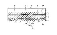
- FIG. 1-1is a perspective view of a main part of the solar cell module 100.
- FIG. 1-2is a plan view of the solar cell module 100 as viewed from the light receiving surface 1a side.
- FIG. 1-3is a cross-sectional view of the solar cell module 100 in FIG. 1-2 cut along a line segment connecting point A and point A ′.
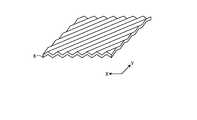
- 1-4is a perspective view for explaining the configuration of the light reflector in the solar cell module 100.
- FIG. 1-1is a perspective view of a main part of the solar cell module 100.
- FIG. 1-2is a plan view of the solar cell module 100 as viewed from the light receiving surface 1a side.
- FIG. 1-3is a cross-sectional view of the solar cell module 100 in FIG. 1-2 cut along a line segment connecting point A and point A ′.
- 1-4is a perspective view for explaining the configuration of the light reflector in the solar cell module 100.
- the solar cell module 100includes an element array DA, a transparent support (substrate) 1, a weather resistant resin film (back surface protective material) 3, a sealing resin (first sealing portion) 41, a sealing resin (second sealing). Stop portion) 42, inter-element connection line 5, and black light reflector 6.
- a plurality of photovoltaic elements 2are spaced apart from each other and arranged substantially on one surface (for example, two-dimensionally).
- the photovoltaic element 2is made of, for example, polycrystalline silicon, single crystal silicon, a double-sided power generation solar cell, or the like.
- the photovoltaic element 2absorbs light having a wavelength within the absorption wavelength range of the received light, and generates a charge separation state according to the absorbed light (generates power).
- Each photovoltaic element 2has a first main surface 2a and a second main surface 2b.
- a metal electrode(see metal electrode 8 shown in FIG. 5A) is disposed on the first main surface 2a.
- the metal electrodeincludes, for example, a plurality of line patterns that respectively intersect with the inter-element connection lines 5.
- An electrode(see the back electrode 9 shown in FIG. 5-4) is disposed on the second main surface 2b. This electrode is formed, for example, so as to cover the second main surface 2b. This electrode does not necessarily need to cover the entire second main surface 2b, and may be a solar cell that is locally present and capable of generating power by light incident from the second main surface 2b.
- the transparent support 1is arranged on the light incident side with respect to the element array DA.
- the transparent support 1has light transparency, and is formed of a light-transmissive material (for example, plate glass) such as transparent glass. In FIG. 1-2, the transparent support 1 is not shown.
- the weather resistant resin film 3is arranged on the side opposite to the light incident side with respect to the element array DA.
- the weather resistant resin film 3is formed of, for example, a weather resistant polyethylene terephthalate resin or a polyethylene terephthalate resin kneaded with a white pigment as a reflective material.
- the protective materialdoes not necessarily need to be an organic film, and may be, for example, an uneven glass.
- the sealing resin 41is disposed between the element array DA and the transparent support 1.
- the sealing resin 42is disposed between the element array DA and the weather resistant resin film 3.
- Each of the sealing resin 41 and the sealing resin 42has light transmittance, and is formed of a transparent sealing material such as ethylene vinyl acetate resin (EVA).
- EVAethylene vinyl acetate resin
- the inter-element connection line 5is formed by connecting the metal electrode on the first main surface 2a of the photovoltaic element 2 to the second main surface of the photovoltaic element 2 adjacent to the photovoltaic element 2 (with a gap). It is connected to the electrode in 2b.
- a copper wireis used as the inter-element connection line 5.
- the inter-element connection line 5is soldered and connected to the metal electrode on the first main surface 2a of the photovoltaic element 2, and is soldered to the electrode on the second main surface 2b of the adjacent photovoltaic element 2. Connected.
- the black light reflector 6is disposed at the interface between the weather resistant resin film 3 and the sealing resin 42.
- the black light reflector 6has a light reflectance of 15% or less over a wavelength range of 500 nm or more and 600 nm or less, and an absorption wavelength range of the photovoltaic element 2 (crystalline silicon) in one of 350 nm or less and 700 nm or more.
- the wavelength selectivityhas a region where the reflectance of light is larger than 15% in the wavelength region overlapping with the.
- the black light reflector 6has, for example, such wavelength selectivity, and is formed of an aluminum foil that has been subjected to blackening treatment (black alumite treatment) by anodization using perylene or the like. In addition to this, it is also possible to use titanium or the like whose surface is oxidized to a thickness of about 20 to 60 nm as shown in Japanese Patent Laid-Open No. 2008-13833 and shows blue due to light interference.
- the black light reflector 6tends not to appear black. Thereby, when the solar cell module 100 is viewed from the light receiving surface 1a side of the transparent support 1, the difference between the color tone of the black light reflector 6 and the color tone (black) of the photovoltaic element 2 becomes conspicuous.
- the black light reflector 6has a light reflectance of 15% or less over a wavelength range of 500 nm to 600 nm. Thereby, since the black light reflector 6 looks black, the difference between the color tone of the black light reflector 6 and the color tone (black) of the photovoltaic element 2 is not conspicuous.
- the reflectance of lightis 15% or less over the wavelength range overlapping the absorption wavelength range of the photovoltaic element 2 at 350 nm or less and 700 nm or more.
- the light intensity of the light reflected by the black light reflector 6is small, and is attenuated to a level that does not contribute to the power generation output before reaching the photovoltaic element 2. This makes it difficult to guide the light reflected by the black light reflector 6 to the photovoltaic element 2.
- the black light reflector 6has a light reflectance of 15 in a wavelength region overlapping with the absorption wavelength range of the photovoltaic element 2 (crystalline silicon) in one of 350 nm or less and 700 nm or more. % Has a region that is greater than%. As a result, the light reflected by the black light reflector 6 has a sufficiently large light intensity at a wavelength that cannot be seen by human eyes and that contributes to power generation, and this is guided to the photovoltaic element 2 to generate power. Can contribute.
- the power generation output of the modulecan be improved.
- the black light reflector 6can be formed of an interference dielectric film, the reflection wavelength shifts depending on the incident angle of light, so it may not necessarily be black depending on the viewing angle.
- the black light reflector 6has a total integrated scattering (TIS) of less than 50% (for example, 30% or less).
- TIStotal integrated scattering
- the total integral scatteringis a numerical value indicating the ratio of the scattered light to the reflected light, and is measured based on the method of American Society for Materials and Testing (ASTM) F1048-87 (1999).
- the total integrated scattering of the light reflector in the present embodimentpreferably takes as small a value as possible in a wavelength region that overlaps the absorption wavelength range of the photovoltaic element at one of 350 nm or less or 700 nm or more, and varies depending on the module structure.
- the total integral scatteringis large, the light reflected by the reflector is scattered at the time of reflection, the incident angle to the interface between the transparent support 1 (glass) and the atmosphere is not constant, and the criticality that causes total reflection.
- the incident light componentis smaller than the angle ⁇ , and a large amount of light is transmitted through the interface between the transparent support 1 (glass) and the atmosphere, and the same light reflector is used as a diffuse reflection (Lambertian reflection). Light can be guided to the photovoltaic element only to the same extent as when it is used.
- the total integrated scatteringis inversely proportional to the square of the wavelength. Integral scattering can also be inferred.
- the total integral scatteringis approximately proportional to the square of the surface roughness (arithmetic average roughness of the surface) of the light reflecting layer, so that the surface roughness is smaller for use as the light reflector in the first embodiment. preferable.
- the incident angle of the light reflected from the black light reflector 6 to the interface between the transparent support 1 (glass) and the atmosphereis critical.
- the total integrated scattering of the black light reflector 6is larger than 50%.
- the reflective surface of the black light reflector 6satisfies the formula (2) or the formula (3).
- the incident angle of the light reflected from the black light reflector 6 on the transparent support 1 (glass)is smaller than the critical angle ⁇ and is likely to be refracted and transmitted without being reflected. This makes it difficult to guide the light reflected by the black light reflector 6 to the photovoltaic element 2.
- the degreevaries depending on the refractive index of the medium constituting the module, the surface flatness of the transparent support, and the spacing between the photovoltaic elements, there is a scatterer that is close to the perfect diffusion generally used so far.
- a reflector embedded in a medium having a refractive index of 1.5is used, about half of the light reflected from the diffuse reflector is transmitted with the incident angle on the transparent support 1 (glass) being smaller than the critical angle ⁇ . Therefore, there is a problem that the light use efficiency is low.
- the regular reflection property of the light reflected by the reflection surfaces 6a11 and 6a12 of the black light reflector 6is high.
- the inclination angle of the reflective surfaces 6a11 and 6a12 in the black light reflector 6is a value equal to or larger than ⁇ satisfying Expression (3), the light reflected from the black light reflector 6 is directed to the transparent support 1 (glass). Becomes larger than the critical angle ⁇ , and the light reflected from the black light reflector 6 can be easily totally reflected. Thereby, it becomes easy to efficiently guide the light reflected by the black light reflector 6 to the photovoltaic element 2.
- the angle of inclination of the reflecting surface of the black light reflector 6is a value smaller than ⁇ that satisfies Equation (3).
- the incident angle of the light reflected from the black light reflector 6 on the transparent support 1 (glass)is critical even if the regular reflection of the light reflected by the reflecting surface of the black light reflector 6 is high.
- the angleis smaller than the angle ⁇ and refracted and transmitted without being reflected. This makes it difficult to guide the light reflected by the black light reflector 6 to the photovoltaic element 2.
- the light incident side surface 6a of the black light reflector 6is inclined with respect to the light receiving surface 1a of the transparent support 1 at an angle equal to or greater than ⁇ satisfying Equation (3).
- a plurality of convex portions 6a1 each having 6a11 and 6a12are included.
- the specific shape of the black light reflector 6is, for example, as shown in FIGS. That is, the light incident side surface 6a of the black light reflector 6 is formed to be a surface in which triangular prisms are repeatedly arranged horizontally. As an example in which the extending direction of the triangular prism is angled with respect to the end of the solar cell module 100, a plane parallel to the inclined surface (light reflecting surface) of the black light reflector 6 and the surface of the solar cell module 100 (light receiving surface 1a).
- FIGS. 1-2 to 1-4show the case of a light reflector in which the line of intersection with () is arranged at 45 °. In FIGS.
- the black light reflector 6has a surface structure in which a triangular prism is tilted sideways, and the ridgeline of the triangular prism (the slope of the black light reflector 6 (light reflecting surface)).
- the vertical direction of the lattice formed by the gap between the photovoltaic elements 2 adjacent to each other in the in-plane directionis parallel to the line of intersection between the plane parallel to the surface and the surface of the solar cell module 100 (light receiving surface 1a) (see FIG. 1-2, and arranged at an angle of 45 ° with respect to the side in the Y direction in FIG. 1-4 or in the horizontal direction (X direction in FIG. 1-2).
- the black light reflector 6may have a plurality of pyramidal convex portions on the light incident side surface 6a.
- the black light reflector 6 arranged in this wayis a light reflector having a shape excellent in mass productivity. For this reason, the black light reflector 6 itself is excellent in mass productivity, and alignment is not required when the solar cell module 100 is manufactured using the black light reflector 6, and the mass light productivity is excellent.
- the solar cell module 100 with an increased amount of light guided to the element 2)can be produced.
- the lightis incident on the light incident side surface (light receiving surface 1a) of the solar cell module 100, passes between adjacent photovoltaic elements 2, and reaches the surface opposite to the light incident side of the solar cell module 100.
- a part of the wavelength region other than visible lightis reflected by the black light reflector 6.
- the light reflected by the black light reflector 6is further reflected at the interface between the atmosphere and the solar cell module 100 and guided to the photovoltaic element 2.
- the sealing resin 42 of the solar cell module 100is made of a general EVA resin
- the refractive index of the EVA resinis about 1.5
- the critical angleis about 42 from Equation (2). °.
- the angle formed by the slope of the black light reflector 6 and the light receiving surface 1a of the solar cell module 100needs to be 21 ° or more from Equation (3).
- the reflected light from the black light reflector 6 having an angle of ⁇ or more shown in the above formula (3) with respect to the light receiving surface 1ais reflected at the transparent support 1 (glass) -air interface and is reflected on the light receiving surface 1a.
- the lightis guided in a parallel direction.
- the angle formed between the light receiving surface 1a of the solar cell module 100 and the inclined surface (light reflecting surface) of the black light reflector 6becomes too large (for example, 2 ⁇ or more), the adjacent black light reflection is performed.
- the lightis multiple-reflected with the slope (light reflecting surface) of the body 6, the incident angle ⁇ of the reflected light from the black light reflector 6 on the glass-atmosphere interface increases, and the reflected light is emitted from the glass. As a result, the light guide efficiency is reduced.
- the black light reflector 6is incident on the light receiving surface 1a of the solar cell module 100 by setting the black light reflector 6 so as to form an angle of about 30 ° ( ⁇ 21 °, ⁇ 42 °) with respect to the light receiving surface 1a.
- the light guide distance of light in a wavelength region other than visible light in the direction parallel to the light receiving surface 1ais increased, and in particular, the power generation output can be improved.
- the solar cell module 100has light reflectivity with respect to light in a wavelength region other than visible light among light incident on the surface of the solar cell module 100 (wavelength selectivity is increased).
- the black light reflector 6 made of an alumite-treated aluminum foilis provided at the interface between the weather resistant resin film 3 and the sealing resin 42 in the solar cell module 100.
- the black light reflector 6is mainly configured by the light receiving surface 1a of the solar cell module 100 and an inclined surface (light reflecting surface) that forms an angle equal to or larger than ⁇ that satisfies the above formula (3).
- the surface shapecan be, for example, a shape in which triangular prisms are arranged in parallel (a shape in which prisms are arranged in parallel). Examples of the shape of the triangular prism include Japanese Patent No. 3616568 and Japanese Patent No. 3433224.
- the light that has entered the light receiving surface 1a of the solar cell module 100 and has passed through the region between the adjacent photovoltaic elements 2 (non-power generation region)is larger than the critical angle of the solar cell module-air interface.
- the lightis reflected by the black light reflector 6 so as to enter the light receiving surface 1 a of the solar cell module 100.
- This reflected lightcan be totally reflected at the solar cell module-air interface. That is, the light that has passed through the region (non-power generation region) between the adjacent photovoltaic elements 2 can be effectively guided to the photovoltaic element 2.
- the solar cell module 100since the total integral scattering is low and the specular reflectance is high, the wavelength region other than the visible light that has passed through the region between the adjacent photovoltaic elements 2 is used. Light can be efficiently re-incident on the photovoltaic element 2 to increase the light utilization efficiency, and the power generation output can be improved. At the same time, by absorbing visible light, the solar cell module 100 with high designability is realized by unifying the color tone of the photovoltaic element and its gap. That is, the power generation output of the solar cell module 100 can be improved and the design of the solar cell module 100 can be improved.
- a metal filmfor example, an aluminum film that is a portion remaining in the aluminum foil without being anodized as described later
- this metal filmcan prevent the penetration of moisture from the outside of the solar cell module 100 into the solar electric element. Thereby, the solar cell module 100 having high reliability is realized.
- the black light reflector 6 having the concavo-convex structureis used as the black light reflector provided in contact with the weather resistant resin film (back surface protective material) 3, but the black light scattering is used instead of the black light reflector. You may use the material.
- the light incident on the black light scattering materialis scattered in various directions, the incident angle on the transparent support 1 (glass) easily becomes larger than the critical angle ⁇ , and is totally reflected at the interface between the glass and the atmosphere. The As a result, light can be guided to the photovoltaic element 2, which can contribute to power generation and can have a uniform appearance. In this case, the black scatterer does not necessarily have unevenness.
- the light scattering portionabsorbs most of the light in the visible region out of the light incident on the non-power generation region by the light scattering portion and exhibits a black color tone. By making it scatter by, it can re-enter into the photovoltaic element 2, and can improve the utilization efficiency of light. That is, the power generation output of the solar cell module 100 can be improved and the design of the solar cell module 100 can be improved.
- a solar battery cell having electrodes on both surfaces of the two main surfaces of the solar battery cellis used, but there is no electrode on the main surface side which is a main light receiving surface, and on the opposite main surface.
- a back contact cell in which only electrodes are arrangedmay be used.
- FIGS. 2-1 to 2-3are cross-sectional views illustrating an example of a method for manufacturing the solar cell module 100 according to the first embodiment.
- a sheet-shaped sealing resin 41iis placed on the transparent support 1 (for example, a transparent glass substrate).
- the sealing resin 41iis made of, for example, ethylene vinyl acetate resin (EVA).
- EVAethylene vinyl acetate resin
- the sheet-shaped sealing resin 42iis placed on the plurality of cells 2.
- the sealing resin 42iis made of, for example, ethylene vinyl acetate resin (EVA).
- EVAethylene vinyl acetate resin
- a weather-resistant polyethylene terephthalate filmis used as the weather-resistant resin film 3i, and an aluminum foil is adhered to the surface as the black light reflector 6i.
- the aluminum foilis black anodized by anodic oxidation using perylene or the like so that the surface of the aluminum foil becomes black.
- the weather resistant resin film 3i to which the black light reflector 6i is adheredis formed.
- This weather resistant resin film 3iis placed on the sealing resin 42i so that the black light reflector 6i is on the light receiving surface 1a side (EVA side).
- the transparent support 1, the sealing resin 41i, the element array DA, the sealing resin 42i, and the weather resistant resin film 3iare sequentially stacked and arranged.
- the element array DAis sealed with a sealing material (sealing resin 41i, sealing resin 42i) between the transparent support 1 and the weather resistant resin film 3. .
- the light incident side surface 6a of the black light reflector 6is formed so as to include a plurality of convex portions 6a1 each having reflection surfaces 6a11 and 6a12 that are inclined at an angle of ⁇ or more that satisfies Equation (3).
- the black light reflector 6iis press-molded. That is, in order to make the black light reflector 6i uneven, a hard plate with unevenness thereon, for example, an unevenness corresponding to the shape shown in FIGS.
- the molds 21are stacked (FIG. 2-2).
- the slopes of the respective pyramid-shaped convex portionsare formed so as to form an angle equal to or larger than ⁇ satisfying Expression (3) with the light receiving surface 1a of the transparent support 1 (transparent glass substrate).
- the entire laminated body in which the transparent support 1, the sealing resin 41i, the element array DA, the sealing resin 42i, and the weather resistant resin film 3i are sequentially laminatedis sandwiched between diaphragms.
- the laminateis heated to a temperature equal to or higher than the softening point of the sealing material (sealing resin 41i, sealing resin 42i) under reduced pressure to soften the sealing material.
- Pressureis applied between the transparent support 1 (transparent glass substrate), the sealing resin 41i and the sealing resin 42i (two weather-resistant polyethylene terephthalate films), and between the sealing resin 41i and the sealing resin 42i (EVA Press between the sheets (Fig. 2-3).
- the solar cell module 100is formed.
- the black light reflector 6 having wavelength selectivityis applied to the weather resistant resin film 3 and the sealing resin 42 on the back surface of the solar cell module 100.
- the light incident surface 6a of the black light reflector 6has a plurality of reflecting surfaces 6a11 and 6a12 that are inclined with respect to the light receiving surface 1a of the transparent support 1 at an angle equal to or larger than ⁇ satisfying Expression (3).
- the black light reflector 6iis embossed so as to include the convex portion 6a1.
- the method for manufacturing the solar cell module 100 according to the first embodimentlight incident on the non-power generation region of the solar cell module 100 can be re-incident on the photovoltaic element 2 to increase the light utilization efficiency.
- the power generation outputcan be increased, and the solar cell module 100 excellent in design can be manufactured.
- the metal film(the aluminum film remaining without being anodized in the aluminum foil) is moisture or salt from the outside of the module to the outside of the module. Therefore, the solar cell module 100 having high reliability can be manufactured.
- the light incident on the non-power generation region where the photovoltaic element 2 does not existcan be guided to the photovoltaic element 2, and the photovoltaic element
- the solar cell module 100having a high reliability and a high design property and excellent in power generation output, with a difference in color tone between the solar cell and the photovoltaic device itself, or between the front and back surfaces of the photovoltaic device is reduced. Can be manufactured.
- the photovoltaic element 2may be a double-sided power generation element.
- the black light reflector 6is arranged on the second main surface 2b side (surface side with low power generation efficiency) of the photovoltaic element 2, from the first main surface 2a of the photovoltaic element 2
- the incident light transmitted through the second main surface 2 b of the photovoltaic element 2can be reflected by the black light reflector 6 and guided again to the photovoltaic element 2.
- the solar cell module 100 provided with the photovoltaic element 2 excellent in the electric power generation outputcan be obtained.
- a see-through solar cell modulethat can take in outdoor light by covering the entire back surface of the solar cell module 100 with a transparent material (the weather-resistant resin film 3 is formed of a light-transmitting material).
- the appearance on the second main surface 2b side of the photovoltaic element 2is equivalent to the appearance on the first main surface 2a side, and the solar cell module 100 excellent in design can be obtained. .
- the light incident side surface of the black light reflector 6is located between the region corresponding to the photovoltaic element 2 and the adjacent photovoltaic element 2.
- the inclination angle formed by the light reflecting surface with respect to the light receiving surface 1a of the transparent support 1may be different from the corresponding region. That is, the black light reflector 6 includes the first light reflection region positioned between the plurality of photovoltaic elements 2 when viewed from the direction perpendicular to the light receiving surface 1 a of the transparent support 1, and the transparent support 1. And a second light reflection region overlapping the photovoltaic element 2 when viewed from a direction perpendicular to the light receiving surface 1a.
- the first light reflection regionincludes the plurality of convex portions 6a1 described above.
- the second light reflecting regionincludes a plurality of second convex portions each having a reflecting surface inclined at an angle smaller than ⁇ satisfying Equation (3) with respect to the light receiving surface 1 a of the transparent support 1.
- the angle at which the light reflected from the second light reflecting region is incident on the main surface 2b side of the photovoltaic element 2is smaller in the light reflection rate on the main surface 2b of the photovoltaic element 2 when it is closer to the vertical. Therefore, since the power generation efficiency is increased, it is preferable that the second light reflection region has no convex portion.
- the power generation efficiency of the solar cell module 100can be further improved.
- the black light reflector 6may be planar, but may be constituted by a light reflecting surface having an angle of ⁇ or more satisfying the mathematical formula (3) with the light receiving surface 1a of the solar cell module 100, and adjacent to the light receiving surface 1a.
- the one that is advantageous for the power generation outputcan be selected.
- the interval between adjacent photovoltaic elementsis as narrow as 1 mm or less, and is incident between adjacent photovoltaic elements.
- the gain by reflecting light to the photovoltaic elementis not so large. Therefore, in this case, the black light reflector 6 may be formed flat on the entire surface (back surface) opposite to the light incident side of the solar cell module 100.
- the black light reflector 6may be formed of a material mainly composed of at least one substance selected from the group consisting of tin, nickel, aluminum, zinc, titanium, copper, and silver. That is, in the black light reflector 6, at least one surface of at least one substance (one metal or an alloy of a plurality of metals) selected from the group consisting of tin, nickel, aluminum, zinc, titanium, copper, and silver is oxidized. (Anodization) may be formed.
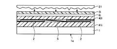
- FIG. 3Ais a cross-sectional view taken along the line connecting the point B and the point B ′ in FIG. 1-2 for illustrating a configuration example of the solar cell module 100j according to the second embodiment.
- FIG. 3-2is a cross-sectional view taken along a line segment connecting the point A and the point A ′ in FIG. 1-2 for illustrating another configuration example of the solar cell module 100j according to the second embodiment. It is. Below, it demonstrates focusing on a different part from Embodiment 1.
- the solar cell module 100jincludes a sealing resin 41j and a sealing resin 42j.
- Sealing resin 42jfunctions as a black scattering portion. That is, the sealing resin 42j is formed of, for example, an ethylene vinyl acetate resin (EVA resin) kneaded with Black 411A pigment of Shepherd Color Company or Brown 10C873 pigment of the company.
- EVA resinethylene vinyl acetate resin
- the sealing resin 42jpreferably has a high light scattering property in order to effectively totally reflect light at the interface between the atmosphere and the glass 1, and preferably has a total integral scattering of 50% or more.
- the sealing resin 42jis formed by kneading, for example, Black 411A pigment of Shepherd® Color Company, Brown® 10C873 pigment of the company, etc., having such wavelength selectivity.
- a typical crystalline silicon solar cell with an antireflection filmhas a light reflectance of about 10% or less in a wavelength region of 500 nm to 600 nm, and a reflectance near 400 nm is about 30% or less.
- the reflectanceneeds to be about 15% or less, and preferably about 10% or less.
- the sealing resin 42jis not necessarily required to have a low light reflectance at all wavelengths in the visible region, and a color that matches the color tone of the photovoltaic element 2 can be selected.
- the company's Blueis used as an additive to the sealing resin 42j to match the color tone. Blue and purple pigments such as 30C588 pigment and Holbein's coloring material Ultramarine Deep, and mixtures thereof can be used.
- the reflectance near 400 nmmay be high, while the reflectance needs to be 15% or less in the wavelength range of about 500 nm to 600 nm.
- a crystalline silicon solar battery cell with an antireflection filmhas a light reflectance of 10% or less in a wavelength region of 500 nm to 600 nm, and in order to match the color tone with this, it is about 500 nm to 600 nm.
- the reflectanceis preferably about 10% or less in the wavelength range.
- the light scattering portion 16jcan be added as shown in FIG.
- the light scattering unit 16jincludes a plurality of black scatterers (a plurality of first light scatterers) 161j and a plurality of black scatterers (a plurality of second light scatterers) 162j.
- Each of the black scatterer 161j and the black scatterer 162jhas a light reflectance of 15% or less over a wavelength region of 500 nm or more and 600 nm or less, and the photovoltaic element 2 (crystal system) in one of 350 nm or less and 700 nm or more
- the wavelength selectivityhas a region where the reflectance of light is greater than 15% in a wavelength region overlapping the absorption wavelength range of silicon.
- Each of the black scatterer 161j and the black scatterer 162jis formed of, for example, Black 411A pigment manufactured by Shepherd® Color® Company or Brown® 10C873 pigment manufactured by the company, having such wavelength selectivity.
- the black scatterers 161j and 162jdo not necessarily have a low light reflectance at all wavelengths in the visible region, and can be selected to have a color that matches the color tone of the photovoltaic element 2.
- the companyuses the black scatterer 161j and the black scatterer 162j to match the color tone.
- Blue to purple pigmentssuch as Blue 30C588 pigment and Ultramarine Deep, a color material of Holbein, and mixtures thereof can be used.
- the black scatterer 161jis disposed between the plurality of photovoltaic elements 2 at the interface between the sealing resin 41j and the sealing resin 42j.
- the black scatterer 162jcovers the second main surface 2b of each of the plurality of photovoltaic elements 2.
- the light intensity reflected from the black scatterer 161jis high, and the light intensity at which the incident angle ⁇ of the light to the glass is not less than the angle (critical angle) satisfying the condition of the above formula (3) is high.
- titania particles or the like having high scattering propertiesmay be mixed with the pigment.
- the light scattering portion 16jmay be a light reflector.
- the surface 42ja on the light incident sideis a reflective surface 42ja11 that is inclined with respect to the light receiving surface 1a of the transparent support 1 at an angle equal to or greater than ⁇ that satisfies Equation (3).
- a plurality of convex portions 42ja1 each having 42ja12are included.
- the same material as the black light reflector 6can be used for the reflecting surface.
- the thickness of the photovoltaic element 2is about 300 nm to 500 ⁇ m, and the thickness of the sealing resins 41j and 42j for sealing the photovoltaic element 2 is about 100 ⁇ m to several millimeters. At this time, the thicknesses of the black scatterers 161j and 162j are large enough to fit into the sealing resins 41j and 42j, and are several ⁇ m to several hundred ⁇ m. The thicknesses of the black scatterers 161j and 162j can be appropriately changed according to the configuration of the solar cell module 100j.
- the scatterer used in the sealing resin 42j, the black scatterer 161j, and the black scatterer 162jpreferably have a total integral scattering of about 50% or more.
- the ratio of the incident light component that is equal to or less than ⁇ in Equation (2) of the spectral solid angle reflectance (spectral reflectance factor) or bidirectional reflection distribution function (BRDF) to total reflected lightIt is preferable to be the largest.
- Spectral solid angle reflectivityis defined in JIS Z8722, and bidirectional reflection distribution function can be measured with reference to ASTM 1392-90 and JIS Z8528-2 Annex C of 2006.
- the total integral scatteringis roughly proportional to the square of the surface roughness (arithmetic mean roughness of the surface) of the light reflecting layer as shown in the following formula (4), and inversely proportional to the square of the wavelength. Therefore, for use as a light scatterer at a target wavelength, the surface roughness is preferably 10 nm to 10 ⁇ m, more preferably 0.1 ⁇ m to 1 ⁇ m.
- TIS1-exp ⁇ (-4 ⁇ / ⁇ ) 2 ⁇ ⁇ (4 ⁇ / ⁇ ) 2 (4)
- ⁇is the root mean square roughness of the light scatterer surface
- ⁇is the wavelength of light.
- the total integral scatteringpreferably satisfies the above range in a wavelength region that overlaps the absorption wavelength range of the photovoltaic device at 350 nm or less or 700 nm or more, but when it is difficult to measure the value at each wavelength, Using the fact that the total integrated scattering is approximately inversely proportional to the square of the wavelength, it is also possible to infer the approximate total integrated scattering at each wavelength from the measured value of one wavelength.
- the particle sizeis composed of particles having a particle size of 100 nm to 10 ⁇ m. .
- the particle size of each of the black scatterer, the black scatterer 161j, and the black scatterer 162j in the sealing resin 42jis smaller than 100 nm.
- the incident angle of the light reflected from the black light reflector 6 to the transparent support 1 (glass)becomes smaller than the critical angle ⁇ and tends to be refracted without being reflected. This makes it difficult to guide the light incident on the black scatterer 161j and the black scatterer 162j to the photovoltaic element 2.
- the particle size of each of the black scatterer, the black scatterer 161j, and the black scatterer 162j in the sealing resin 42jis larger than 10 ⁇ m.
- the incident angle of the light reflected from the black light reflector 6 to the transparent support 1 (glass)becomes smaller than the critical angle ⁇ and tends to be transmitted without being reflected. is there. This makes it difficult to guide the light incident on the black scatterer 161j and the black scatterer 162j to the photovoltaic element 2.
- the particle size of each of the black scatterer, the black scatterer 161j, and the black scatterer 162j in the sealing resin 42jis light in a wavelength region where the amount of sunlight is large.
- the light intensityis 100 nm or more, in which strong light scattering occurs, and the light scattering intensity per volume is sufficiently large, such as about several tens of ⁇ m or less.
- the incident angle of the incident light on the transparent support 1 (glass)easily becomes larger than the critical angle ⁇ , and the light scattered by the sealing resin 42j or the black scatterer 161j can be easily totally reflected. Thereby, it becomes easy to guide the light scattered by the sealing resin 42j or the black scatterer 161j to the photovoltaic element 2.
- the solar cell module 100jin the solar cell module 100j, most of the light in the visible region out of the light incident on the non-power generation region is absorbed by the light scattering unit 16j and exhibits a black color tone, but the region other than the visible region By scattering light in the wavelength region by the light scattering portion 16j, the light can be reincident on the photovoltaic element 2 and the light utilization efficiency can be increased. That is, the power generation output of the solar cell module 100j can be improved and the design of the solar cell module 100j can be improved.
- an appropriate pigment or the likeis selected as the material of the light scattering portion 16j, and a part of light in the visible region that is the light absorption region of the photovoltaic element 2 is absorbed.
- a light scatterer that scatters some other lightcan be used. Thereby, a part of the light in the visible region incident on the non-power generation region between the photovoltaic elements 2 is absorbed by the light scattering unit 16j, and the other part of the light in the visible region is scattered by the light scattering unit 16j. Colors including blue, red, yellow, etc. other than white can be provided in the non-power generation region.
- the designis made by making the color tone of the non-power generation region closer to the color tone of the photovoltaic element 2. Therefore, it is possible to realize the solar cell module 100j that is excellent in power generation output and excellent in design.
- a solar battery cell having electrodes on both surfaces of the two main surfaces of the solar battery cellis used, but there is no electrode on the main surface side which is a main light receiving surface, and on the opposite main surface.
- a back contact cell in which only electrodes are arrangedmay be used.
- FIGS. 4-1 to 4-4are cross-sectional views illustrating the method for manufacturing the solar cell module 100j according to the second embodiment. The following description will focus on differences from the manufacturing method shown in FIGS. 2-1 to 2-3.
- the sealing resins 41j1 and 42j1do not necessarily have an uneven shape on the surface, but the scattering angle distribution of light scattering of the sealing resin 42j1 and the black scatterer 161j is small, and the scattering intensity in the direction perpendicular to the scattering surface is high.
- the light scattering surface of the sealing resin 42j1 or the black scatterer 161jis inclined with respect to the surface of the solar battery module 100j, more light can be guided to the solar battery cell.
- the surface of the sealing resin 42j1 or the black scatterer 161jis provided with irregularities, but it may be made flat for ease of manufacturing. Further, for the above purpose, the surface shape does not necessarily have a regular uneven structure.
- a sheet-like sealing resin 41j1is placed on the transparent support 1, and then a mold 21 (see FIG. 2-2) with projections and recesses is overlaid to seal the sealing resin 41j1. Is embossed. Thereby, a plurality of convex portions having the same shape as the plurality of convex portions 6a1 in the first embodiment are formed on the surface of the sealing resin 41j1 opposite to the light incident side. The other points are the same as those shown in FIG.
- a sealing resin embossed in advancemay be used as the sealing resin 41j1, a sealing resin embossed in advance may be used.
- Brown 10C873 pigment powder of Shepherd Color Companyis applied to the plurality of cells 2 as the black scatterer 161j and the black scatterer 162j.
- the black scatterer powderis composed of particles having a particle size of 100 nm or more and 10 ⁇ m or less.
- the black scatterers 161jare arranged between the plurality of cells 2, and the black scatterers 162j are arranged on the second main surface 2b of each cell 2.
- a sheet-shaped sealing resin 42j1is prepared.
- the sealing resin 42jfor example, an ethylene vinyl acetate resin (EVA) sheet in which the same material as that of the black light reflector 6 is kneaded is used.
- EVAethylene vinyl acetate resin
- the mold 21with projections and depressions is placed on the light incident side surface of the sheet-shaped sealing resin 42j1, and the sealing resin 42j1 is stamped.
- a plurality of convex portions having the same shape as the plurality of convex portions 6a1 in the first embodimentare formed on the light incident side surface of the sealing resin 42j1.
- a sheet-shaped sealing resin 42j1is placed on the plurality of cells 2.
- a sealing resin embossed in advancemay be used as the sealing resin 42j1, a sealing resin embossed in advance may be used.
- the mold 21is not stamped.
- the other pointsare the same as those shown in FIG. 4-4.
- the black scatterer 161jis formed between the adjacent photovoltaic elements 2, and the black scatterer 162j is the first of the photovoltaic elements 2. 2 on the main surface 2b.
- the particle diameter of each of the sealing resin 42j1 or the black scatterer 161j and the black scatterer 162jis a size of 100 nm or more at which strong light scattering occurs, and the volume The scattered light intensity is about several tens of ⁇ m or less.
- the incident angle of the scattered light on the surface of the solar cell module 100jis larger than the critical angle.
- the amount of large lightcan be increased, and the scattered light can be easily totally reflected on the surface of the solar cell module 100j and guided to the photovoltaic element 2.
- the solar cell 2is a solar cell element or the like capable of generating power on both sides and the entire surface of the surface opposite to the main light incident side is not covered with the electrode, it is opposite to the main light incident side of the solar cell 2. Since the sealing resin 42j1 and the black scatterer 162 are provided as light scatterers on the surface, the absorption coefficient of the solar battery cell is small and the light that has been transmitted without being absorbed can be scattered and reflected by the sealing resin 42j1 and the black scatterer 162. The light transmitted through the solar battery cell can be incident on the solar battery again to contribute to power generation.
- the solar cell module 100jin the solar cell module 100j, most of the visible light out of the light incident on the non-power generation region is absorbed by the sealing resin 42j1 and the light scattering portion 16j, and a visible color tone is obtained.
- the lightBy scattering a lot of light in the wavelength region other than the region by the light scattering portion 16j, the light can be re-incident on the photovoltaic element 2 to increase the light use efficiency. That is, the power generation output of the solar cell module 100j can be improved and the design of the solar cell module 100j can be improved.
- the scatterers, the black scatterers 161j, and the black scatterers 162j in the sealing resin 42j1are formed of pigments. Therefore, compared with the case where a black light reflector is formed with a metal, the withstand voltage property between the adjacent photovoltaic elements 2 can be improved, and the manufacturing cost of the solar cell module 100j can be reduced.
- Each of the black scatterer 161j and the black scatterer 162jincludes copper oxide, iron oxide, cobalt oxide, molybdenum oxide, manganese dioxide, chromium oxide, nickel oxide, iron titanate, manganese-containing titanium dioxide, and antimony-containing dioxide dioxide.
- FIG. 5Ais a plan view of the solar cell module 100k as viewed from the light receiving surface 1a side.
- FIG. 5-2is a cross-sectional view showing the configuration of the solar cell module 100k.
- FIG. 5-3is an enlarged cross-sectional view of a portion passing through the soldering bus electrode 12 in the photovoltaic element in the solar cell module 100k.
- FIG. 5-4is an enlarged cross-sectional view of a portion passing through the collector electrode 8 in the photovoltaic element in the solar cell module 100k. Below, it demonstrates centering on a different part from Embodiment 1 and Embodiment 2.
- FIG. 1Ais a plan view of the solar cell module 100k as viewed from the light receiving surface 1a side.
- FIG. 5-2is a cross-sectional view showing the configuration of the solar cell module 100k.
- FIG. 5-3is an enlarged cross-sectional view of a portion passing through the soldering bus electrode 12 in the photovoltaic element in the solar cell
- the solar cell module 100kincludes a light scattering portion 16k.
- the light scattering unit 16kincludes a plurality of black scatterers 161k and 162k.
- Each of the black scatterers 161k and 162khas a light reflectance of 15% or less over a wavelength range of 500 nm or more and 600 nm or less, and absorption of the photovoltaic element 2 (crystalline silicon) at one of 350 nm or less and 700 nm or more. It has wavelength selectivity having a region where the reflectance of light is greater than 15% in a wavelength region overlapping the wavelength range.
- each black scatterer 161k, 162kconsists of a particle
- the light scattering portion 16 kincludes a black scatterer (a plurality of third light scatterers) 161 k that covers the current collecting electrode (metal electrode) 8 and a black scatterer 162 k that covers the inter-element connection line 5.
- a black scatterer 161k and 162k that cover the electrodes on the light receiving surface sidefor example, Brown 10C873 pigment powder manufactured by Shepherd Color Company may be used.
- an electrode of about several tens of micrometersis formed on the light incident side surface of the solar battery cell by an aluminum vapor deposition method using a vapor deposition mask, and this is used as perylene. It may be formed by anodic oxidation in the solution. At this time, an electrode having a large surface roughness can be obtained by roughening the surface of the solar cell using reactive ion etching using a reactive gas such as SF6 prior to depositing aluminum. As a result, light scattering properties are exhibited.
- the method of using such a metal electrode directly as a black scattererdoes not require the black scatterer to be formed in accordance with the position of the electrode, so that alignment is not necessary, and the black scatterer is applied to the light receiving surface of the solar battery cell. There is an advantage that the shadow area to be formed can be reduced.
- the first main surface 2a of the photovoltaic element 2may be covered with the antireflection film 10 in a region where the current collecting electrode 8 and the bus electrode 12 are not arranged.
- the antireflection filmis not always essential.
- a back electrode 9is disposed on the second main surface 2 b of the photovoltaic element 2.
- the particle size of the particles in each of the black scatterer 161k and the black scatterer 162kis about 100 nm or more at which light scattering occurs, and the light scattering intensity per volume is sufficiently large. A size of about several tens of ⁇ m or less is preferable.
- the black scatterer 162k covering the inter-element connection line 5is scattered in various directions, the incident angle of the light scattered by the black scatterer 162k on the transparent support 1 (glass) is easy. Therefore, the light scattered by the black scatterer 162k can be easily totally reflected. Thereby, it becomes easy to guide the light scattered by the black scatterer 162k to the photovoltaic element 2.
- the color tone of the current collecting electrode 8 or the inter-element connection line 5 on the light incident side surface of the photovoltaic element and the color tone of the light absorbing portioncan be brought close to each other. it can.
- a large amount of light in the wavelength region other than the visible regioncan be reincident on the photovoltaic element 2 to increase the light utilization efficiency. That is, the power generation output of the solar cell module 100k can be improved and the design of the solar cell module 100k can be improved.
- the manufacturing method of the solar cell module 100k according to the third embodimentis exemplified by a single crystal silicon solar cell module using a single crystal silicon solar cell (hereinafter referred to as cell 2) as the photovoltaic element 2.
- a single crystal silicon solar cellis used as an example, but a thin film solar cell such as an amorphous silicon solar cell or a cadmium tellurium solar cell can be applied when not only a transparent electrode but also a metal electrode or the like is used.
- a texture structure having irregularitiesis formed on the first main surface 2a of a P-type single crystal silicon substrate 11 as a semiconductor substrate.
- An N-type diffusion layer in which N-type impurities such as phosphorus are diffused by applying heat of about 900 ° C. using phosphorus oxychloride as a raw materialis formed in a predetermined depth range from the surface of the silicon substrate 11.
- a semiconductor PN junctionis formed on the surface of the silicon substrate 11.
- a silicon nitride filmis formed on the first main surface 2a of the silicon substrate 11 by a chemical vapor deposition method as an antireflection film 10 for preventing reflection of incident light, and then a paste containing a glass component and silver is formed. Printing is performed on the first main surface 2a of the silicon substrate 11 by a screen printing method.
- a current collecting electrode (grid electrode) 8made of silver or the like provided in a comb shape for locally collecting current (electrons) generated at the surface PN junction of the single crystal silicon substrate 11, and current collecting
- a surface electrode (light receiving)composed of a surface bus electrode 12 made of silver or the like provided so as to connect the current collecting electrodes 8 substantially orthogonal to the current collecting electrodes 8. Electrode on the surface 1a side).
- the second main surface 2b of the P-type silicon substrate 11has aluminum or the like provided on almost the entire second main surface 2b of the P-type silicon substrate 11 for the purpose of collecting electricity generated by the PN junction. Then, the back electrode 9 and the back electrode 12 made of silver or the like for taking out current to the outside are formed by a screen printing method.
- the electrodeis baked by heating at a temperature of about 800 ° C., and the antireflection film is eroded to connect the electrode and the semiconductor substrate.
- a black 411A pigment manufactured by Shepherd® Color Companyis mixed with an aqueous solution of acetylacetone and acetic acid and kneaded to prepare a paste, which is printed as a black scatterer 161k covering the current collecting electrode 8 by a screen printing method.
- a paste made of particles having a particle size of 100 nm to 10 ⁇ mis used.
- the substrateis heated, components other than the pigment are skipped and dried.
- a maskis placed on a portion of the inter-element connection line 5 other than the copper wire, and the thinned paste containing the pigment is applied by spraying so that only the copper wire portion is mainly black. Thereafter, the mixture is heated to about 200 ° C., and components other than the pigment are skipped and dried.
- the light black scatterer 161k and the black scatterer 162kare placed in a region covering the current collecting electrode (metal electrode) 8 and the inter-element connection line 5.
- the particle size of each of the black scatterers 161k and the black scatterers 162kis a size of 100 nm or more at which light scattering occurs, and the light scattering intensity per volume is sufficiently large, about several tens of ⁇ m. It is the following size.
- the light incident on the black scatterer 161k and the black scatterer 162kis scattered in various directions. It can be reflected and guided to the photovoltaic element 2.
- the color tone of the current collecting electrode 8 or the inter-element connection line 5 on the light incident side surface of the photovoltaic element and the color tone of the light absorbing portioncan be brought close to each other. it can.
- light in a wavelength region other than the visible regionis scattered by the black scatterer 161k and the black scatterer 162k, so that the light can be reincident on the photovoltaic element 2 and the light use efficiency can be improved. That is, the power generation output of the solar cell module 100k can be improved and the design of the solar cell module 100k can be improved.
- the current collecting electrode and the black light scattererare separately formed, but it is not always necessary to separate them, and the metal component serving as the electrode and the particles of the black scatterer are mixed. A state is good.
- the black light scatterer 6 covering the electrodefor example, the current collecting electrode 8 on the light incident side surface is formed by an aluminum vapor deposition method using a vapor deposition mask, and this is anodeed in a solution using perylene or the like. It may be formed by oxidation. As a means for blackening, not only oxidation but also sulfurization may be used. The method of using such a metal electrode directly as a black scatterer does not require the black scatterer to be formed in accordance with the position of the electrode, so that alignment is not necessary, and the black scatterer is applied to the light receiving surface of the solar battery cell. There is an advantage that the shadow area to be formed can be reduced.
- the light scattering portiondoes not necessarily have to be in contact with the metal electrode, and may be formed separately, for example, may be embedded in the sealing resin 41.
- Each black scatterer 161k, 162kis made of copper oxide, iron oxide, cobalt oxide, molybdenum oxide, manganese dioxide, chromium oxide, nickel oxide, iron titanate, manganese-containing titanium dioxide, antimony-containing titanium dioxide, manganese-containing.
- a black light reflectormay be used instead of at least one of the black scatterer 161k and the black scatterer 162k. That is, the current collector electrode (metal electrode) 8 may be covered with a black light reflector instead of the black scatterer 161k.
- the inter-element connection line 5may be covered with a black light reflector instead of the black scatterer 162k.
- the black light reflectormay be formed of a material whose main component is at least one substance selected from the group consisting of tin, nickel, aluminum, zinc, titanium, copper, silver, and gold.
- the black scattererhas at least one surface of at least one substance (one metal or an alloy of a plurality of metals) selected from the group consisting of tin, nickel, aluminum, zinc, titanium, copper, silver, and gold. It may be formed by oxidation (anodization or the like).
- a black light reflectorhas an anodized aluminum (aluminum foil) or surface oxidized as shown in Japanese Patent Application Laid-Open No. 2008-13833 with a thickness of about 20-60 nm. You may form with the titanium etc. which show blue.
- a grid-like electrode having a thickness of about several tens of micrometersis formed as a collecting electrode 8 on the light incident side surface of the solar cell by an aluminum vapor deposition method using a vapor deposition mask or the like. It may be formed by anodizing in a solution using the above.
- the surface of the solar cellis made different in a sodium hydroxide solution to which isopropyl alcohol is added prior to vapor deposition of aluminum.
- an electrode having an inclined surface with respect to the surface direction of the substratecan be formed.
- the angle at which the light is reflecteddepends on the module surface. It can be set as an angle more than the critical angle of the translucent material.
- the method of using such a metal electrode directly as a black reflectordoes not require the black reflector to be formed in accordance with the position of the electrode, so that alignment is not necessary, and the black reflector causes the light receiving surface of the solar battery cell to be aligned. There is an advantage that the area of the formed shadow can be reduced.
- the light incident side surface of the black light reflectorhas at least one convex portion each having a reflective surface inclined at an angle of ⁇ or more that satisfies Formula (3) with respect to the light receiving surface 1a of the transparent support 1.
- the black light reflectoris embossed so as to be formed.
- light having a wavelength other than visible light out of the light incident on the first main surface of the photovoltaic elementis incident on the light receiving surface 1a of the transparent support 1 at an angle larger than the critical angle of the solar cell module-air interface.
- the lightis reflected by a black light reflector so as to enter the light. As a result, the reflected light can be totally reflected at the solar cell module-air interface and contribute to power generation.
- the solar cell module, the photovoltaic device, and the method for manufacturing a solar cell module according to the present inventionare useful for photovoltaic elements that are used in a module state.
- SYMBOLS 1Transparent support 1a Light-receiving surface 2 Photovoltaic element 2a 1st main surface 2b 2nd main surface 3, 3i Weather resistant resin film 5 Interelement connection line 6, 6i Black light reflector 6a1 Protrusion 6a11, 6a12 Reflection Surface 8 Current collecting electrode 9 Back surface electrode 10 Antireflection film 11 Silicon substrate 12 Bus electrode 13 Solder 16j, 16k Light scattering portion 41, 41i, 41j, 41j1, 42, 42i, 42j, 42j1 Sealing resin 42ja1 Protruding portion 42ja11, 42ja12 Reflective surface 100, 100j, 100k Solar cell module 161j, 162j, 161k, 162k Black scatterer DA Element arrangement
Landscapes
- Photovoltaic Devices (AREA)
Abstract
Description
Translated fromJapanese本発明は、太陽電池モジュール、光起電力装置、及び太陽電池モジュールの製造方法に関する。The present invention relates to a solar cell module, a photovoltaic device, and a method for manufacturing a solar cell module.
光起電力素子は、その耐候性を高めるため、透明なガラス基板と裏面保護材との間に樹脂によって封止したモジュールの状態で使用に供される。この際、光起電力素子や電気配線の配置のし易さなどから、光起電力素子間に隙間を設けて配置することが多い。ガラス基板の表面(受光面)に入射した光のうち光起電力素子間の隙間を通過する光は、光起電力素子による発電に寄与できない。The photovoltaic element is used in the state of a module sealed with a resin between a transparent glass substrate and a back surface protective material in order to enhance its weather resistance. At this time, in many cases, a gap is provided between the photovoltaic elements because of ease of arrangement of the photovoltaic elements and electrical wiring. Of the light incident on the surface (light receiving surface) of the glass substrate, light passing through the gap between the photovoltaic elements cannot contribute to power generation by the photovoltaic elements.
ガラス基板の表面(受光面)に入射した光のうち光起電力素子間の隙間を通過する光を利用して太陽電池モジュールの発電出力を向上させるためには、光反射率の高い部材を太陽電池モジュールの裏側に配置して光起電力素子間の隙間を通過する光をモジュール内において受光面側に反射させ、受光面側のガラス表面で再反射させるなどして光起電力素子に入射させることが考えられる。In order to improve the power generation output of the solar cell module by using the light incident on the surface (light receiving surface) of the glass substrate and passing through the gaps between the photovoltaic elements, a member having a high light reflectivity is used for the sun. Light that passes through the gap between the photovoltaic elements placed on the back side of the battery module is reflected on the light receiving surface side in the module and re-reflected on the glass surface on the light receiving surface side to enter the photovoltaic elements. It is possible.
この光反射率の高い部材は、可視光領域を含む広い波長領域で光の反射率を高い材料を用いるため、その色調は白等となる。それに対して、光起電力素子は、光の吸収を最大限とするために黒色のものとなることが多い。これにより、受光面側から太陽電池モジュールを見た場合に、光起電力素子と光起電力素子間の隙間とで異なる色調となり、太陽電池モジュールの意匠性が乏しくなってしまう。The member having a high light reflectance uses a material having a high light reflectance in a wide wavelength region including the visible light region, and thus the color tone is white. In contrast, photovoltaic elements are often black in order to maximize light absorption. Thereby, when a solar cell module is seen from the light-receiving surface side, it becomes a different color tone by the photovoltaic element and the clearance gap between photovoltaic elements, and the design property of a solar cell module will become scarce.
意匠性を高めるためには、光反射率の高い部材の代わりに、カーボンブラック等の黒色顔料により黒色に着色し可視光を吸収する部材を太陽電池モジュールの裏側に配置することも考えられる。In order to improve the design, it is conceivable to arrange a member that is colored black with a black pigment such as carbon black and absorbs visible light instead of a member having high light reflectance on the back side of the solar cell module.
この可視光を吸収する部材は、黒色顔料が光を吸収し光を熱へ変換する。このため、太陽電池モジュールの温度が上昇し、太陽電池モジュールの発電出力が低下してしまう。また、光起電力素子間の隙間を通過する光のほぼ全てを無駄にしてしまうため、光反射率の高い部材を配置した場合よりも発電出力が大幅に低下してしまう。∙ In the member that absorbs visible light, the black pigment absorbs light and converts the light into heat. For this reason, the temperature of a solar cell module will rise and the electric power generation output of a solar cell module will fall. In addition, since almost all of the light passing through the gap between the photovoltaic elements is wasted, the power generation output is greatly reduced as compared with the case where a member having a high light reflectance is arranged.
特許文献1には、赤外線反射性積層体において、基材層の一方の面に赤外線透過性のペリレン系黒色顔料で黒色の着色樹脂層を積層し、基材層の他方の面に赤外線反射性の白色顔料で白色の着色樹脂層を積層することが記載されている。そして、黒色の着色樹脂層が可視光を吸収して着色された外観を呈するとともに赤外光を内部に透過させ、その透過された赤外光が白色の着色樹脂層で反射され基材層及び黒色の着色樹脂層を通過して放射されるとされている。これにより、特許文献1によれば、外見的に黒色または有彩色に着色されていても特定波長の赤外線を反射して蓄熱を防止することができるとされている。In
特許文献2には、光学薄膜構造において、基板の上に、赤外光反射層、スペーサ層、可視光を吸収する吸収材を順に積層した光薄膜積層体を形成することが記載されている。この光学薄膜構造では、赤外光反射層で反射した光と吸収材で部分的に反射した光とが干渉しあう。これにより、特許文献2によれば、可視領域及び近赤外領域で低い反射率を達成するとともに、赤外領域及び遠赤外領域で高い反射率と放射率を達成できるので、良好な太陽光吸収体(good solar absorber)を実現することができるとされている。
特許文献3には、太陽電池モジュールにおいて、透光性表面部材と耐候性フィルムとの間に透光性充填材を介して太陽電池素子を挟持するとともに、耐候性フィルムを階段状に形成することが記載されている。この太陽電池モジュールが屋根に設置された場合、耐候性フィルムにおける軒方向面に直接太陽が照射されず散乱光のみが照射される場合が多く、地上の観測者が耐候性フィルムにおける軒方向面のみを視認するので、耐候性フィルムが低反射色に見えるとされている。これにより、特許文献3によれば、太陽電池素子の受光面と太陽電池素子の間から見える耐候性フィルムの軒方向面とがいずれも低反射色に見えるので、両者の色の差により設置外観が損なわれることを低減できるとされている。In
上述のように、太陽電池モジュールの発電出力を向上させることと、太陽電池モジュールの意匠性を向上させることとは、両立させることが困難である。As described above, it is difficult to improve both the power generation output of the solar cell module and the design of the solar cell module.
特許文献1には、赤外線反射性積層体を適用した太陽電池用バックシートを使用した太陽電池モジュールにおいて、太陽光の受光面側から、透明基板、封止膜、太陽電池素子、封止膜、太陽電池用バックシートを順に積層することが記載されている。この太陽電池モジュールでは、透明基板へ入射し太陽電池素子間の隙間を通過した赤外光が、太陽電池用バックシートへ入射することになる。このとき、赤外光が白色の着色樹脂層で反射される前後でそれぞれ2回ずつ黒色の着色樹脂層及び基材層を通過して減衰(部分的に吸収)されるので、太陽電池素子へ十分な強さの赤外光を入射させられない可能性がある。これにより、太陽電池モジュールの発電出力が低下する傾向にある。In
また、特許文献1では、赤外線反射による熱の放射についてのみ述べられており、可視光線以外の光を反射させることによる発電への寄与に関する記述が無く、その構造は必ずしも有効に発電に寄与しないという問題がある。例えば、反射層によって反射された光のうち、モジュール表面への入射角が臨界角以上となる光成分がモジュール表面で全反射され、光起電力素子へ再入射することが可能となるが、反射層と可視光吸収層とが異なる2層として存在し、反射層での光反射が散乱によるものの場合、反射層で反射された光は可視光吸収層あるいは可視光吸収層とモジュール封止材との界面で反射され必ずしも有効に発電に寄与しない。Moreover, in
特許文献2では、可視光吸収特性と赤外線反射特性とを兼ねそろえた太陽熱吸収について述べられているが、反射赤外線を利用した太陽光発電については述べられていない。このような膜をそのまま太陽電池モジュールのバックシート部等に用いても、反射赤外光が有効に太陽電池素子へ導光されず、発電出力向上を得ることができないと考えられる。
また、特許文献2に記載された光学薄膜構造では、光薄膜積層体へ入射した赤外光が、赤外光反射層で反射される前後でそれぞれ2回ずつ吸収材及びスペーサ層を通過して減衰(部分的に吸収)されるので、十分な強さの赤外光を光薄膜積層体から放射できない可能性がある。これにより、この光学薄膜構造を太陽電池モジュールへ適用した場合に、その太陽電池モジュールの発電出力が低下する可能性が高い。Moreover, in the optical thin film structure described in
一方、特許文献3に記載された技術では、一年を通して変化する太陽高度によっては、耐候性フィルムにおける軒方向面に直接太陽が照射されるので、地上の観測者から耐候性フィルムが白色に近い色に見える可能性がある。また、太陽電池モジュールが地上の観測者の目線より低い位置に設置された場合、地上の観測者が耐候性フィルムにおける直接太陽が照射される棟方向面を視認するので、この場合も、地上の観測者から耐候性フィルムが白色に近い色に見える可能性がある。また、一般的に太陽電池モジュール表面に用いられるガラスの表面は、防眩性等のため平坦ではなく凹凸を有しているため、モジュール内部からガラス表面に到達した光はガラス表面に対して局所的に臨界角以下の角度で入射し、全反射しない部分が生じ、太陽電池素子と太陽電池素子との間が明るく見える。これにより、太陽電池素子の受光面と太陽電池素子の間から見える耐候性フィルムの軒方向面との色調が大きく異なり、太陽電池モジュールの意匠性が低下する可能性がある。On the other hand, in the technique described in
また、特許文献1から3には、いずれも、光起電力素子の光入射側の面における金属電極と光吸収部分との色調をどのようにして近づけるのかについて記載がない。多くの金属はプラズマ反射により可視光を反射してしまうため、基板の受光面側から太陽電池モジュールを見た場合に、光起電力素子の光入射側の面における金属電極と光吸収部分とで異なる色調となり、太陽電池モジュール及び光起電力装置の意匠性が乏しくなってしまう。Also, none of
本発明は、上記に鑑みてなされたものであって、太陽電池モジュールの発電出力を向上できるとともに、太陽電池モジュールの意匠性を向上できる太陽電池モジュール、光起電力装置、及び太陽電池モジュールの製造方法を得ることを目的とする。The present invention has been made in view of the above, and can produce a solar cell module, a photovoltaic device, and a solar cell module capable of improving the power generation output of the solar cell module and improving the design of the solar cell module. The purpose is to obtain a method.
上述した課題を解決し、目的を達成するために、本発明の1つの側面にかかる太陽電池モジュールは、光が主に入射する側の第1の主面と、光が主に入射する側の反対側の第2の主面とをそれぞれ有する複数の光起電力素子が配列された素子配列と、前記素子配列に対して光入射側に配された光透過性を有する基板と、前記素子配列と前記基板との間に配された光透過性を有する第1の封止部と、前記素子配列に対して光入射側と反対側に配された裏面保護材と、前記素子配列と前記裏面保護材との間に配された第2の封止部と、前記第1の封止部、前記第2の封止部、前記裏面保護材、及び前記基板のうちの少なくとも1つの内部における前記複数の光起電力素子間の隙間に対応した領域に配された光散乱部とを備え、前記光散乱部は、500nm以上600nm以下の波長域に渡って光の反射率が15%以下であり、かつ、350nm以下及び700nm以上の一方における前記光起電力素子の吸収波長範囲に重なる波長域に光の反射率が15%より大きくなる領域を有する波長選択性を有し、前記光散乱部の全積分散乱は、350nm以下及び700nm以上の一方における前記光起電力素子の吸収波長範囲に重なる波長域において50%以上となることを特徴とする。In order to solve the above-described problems and achieve the object, a solar cell module according to one aspect of the present invention includes a first main surface on a side where light is mainly incident and a side on which light is mainly incident. An element array in which a plurality of photovoltaic elements each having a second main surface on the opposite side are arrayed, a light-transmitting substrate disposed on the light incident side with respect to the element array, and the element array A light-transmitting first sealing portion disposed between the substrate and the substrate; a back surface protective material disposed on a side opposite to the light incident side with respect to the element array; and the element array and the back surface A second sealing portion disposed between the protective material, the first sealing portion, the second sealing portion, the back surface protective material, and the substrate in at least one of the substrates. A light scattering portion disposed in a region corresponding to a gap between a plurality of photovoltaic elements, the light scattering portion, The reflectance of light is 15% or less over the wavelength range of 00 nm or more and 600 nm or less, and the reflectance of light is in a wavelength range that overlaps the absorption wavelength range of the photovoltaic element in one of 350 nm or less and 700 nm or more. Having a wavelength selectivity having a region larger than 15%, and the total integrated scattering of the light scattering portion is 50% or more in a wavelength region overlapping with the absorption wavelength range of the photovoltaic element in one of 350 nm or less and 700 nm or more It is characterized by becoming.
本発明の他の側面にかかる太陽電池モジュールは、複数の光起電力素子が配列された素子配列と、前記素子配列に対して光が主に入射する側に配された光透過性を有する基板と、前記素子配列と前記基板との間に配された光透過性を有する第1の封止部と、前記素子配列に対して光が主に入射する側の反対側に配された裏面保護材と、前記素子配列と前記裏面保護材との間に配された第2の封止部と、前記第1の封止部、前記第2の封止材、前記裏面保護材、及び前記基板のうち少なくとも1つの内部における前記複数の光起電力素子間の隙間に対応した領域に配された光反射部とを備え、前記光反射部は、500nm以上600nm以下の波長域に渡って光の反射率が15%以下であり、かつ、350nm以下及び700nm以上の一方における前記光起電力素子の吸収波長範囲に重なる波長域に光の反射率が15%より大きくなる領域を有する波長選択性を有し、前記光反射部の全積分散乱は、350nm以下及び700nm以上の一方における前記光起電力素子の吸収波長範囲に重なる波長域において50%未満であり、前記光反射部における光入射側の面は、前記光反射部が接する媒体の屈折率をnとしたとき、前記基板の受光面に対してα = (arcsin(1/n))/2を満たすα以上の角度で傾斜した反射面をそれぞれ有する複数の斜面を含むことを特徴とする。A solar cell module according to another aspect of the present invention includes an element array in which a plurality of photovoltaic elements are arrayed, and a light-transmitting substrate disposed on a side where light mainly enters the element array. And a first sealing portion having light transmittance disposed between the element array and the substrate, and a back surface protection disposed on the opposite side of the element array to the side on which light is mainly incident. A material, a second sealing portion disposed between the element array and the back surface protective material, the first sealing portion, the second sealing material, the back surface protective material, and the substrate A light reflecting portion disposed in a region corresponding to a gap between the plurality of photovoltaic elements in at least one of the plurality of photovoltaic elements, and the light reflecting portion transmits light over a wavelength range of 500 nm to 600 nm. Reflectivity is 15% or less and one of 350 nm or less and 700 nm or more A wavelength selectivity having a region in which the reflectance of light is greater than 15% in a wavelength region overlapping the absorption wavelength range of the photovoltaic device, and total integrated scattering of the light reflecting portion is 350 nm or less and 700 nm or more When the refractive index of the medium in contact with the light reflecting portion is n, the surface on the light incident side of the light reflecting portion is less than 50% in the wavelength region overlapping the absorption wavelength range of the photovoltaic element in one of And a plurality of inclined surfaces each having a reflecting surface inclined at an angle of α or more satisfying α = (arcsin (1 / n)) / 2 with respect to the light receiving surface of the substrate.
本発明の他の側面にかかる太陽電池モジュールは、金属電極が配された光が主に入射する側の第1の主面と、光が主に入射する側の反対側の第2の主面とをそれぞれ有する複数の光起電力素子が配列された素子配列と、前記素子配列に対して光入射側に配された光透過性を有する基板と、前記素子配列と前記基板との間に配された光透過性を有する第1の封止部と、前記素子配列に対して光入射側と反対側に配された裏面保護材と、前記素子配列と前記裏面保護材との間に配された第2の封止部と、前記複数の光起電力素子のそれぞれの前記第1の主面における前記金属電極を覆う領域に配された光散乱部とを備え、前記光散乱部は、500nm以上600nm以下の波長域に渡って光の反射率が15%以下であり、かつ、350nm以下及び700nm以上の一方における前記光起電力素子の吸収波長範囲に重なる波長域に光の反射率が15%より大きくなる領域を有する波長選択性を有し、前記光散乱部の全積分散乱は、350nm以下及び700nm以上の一方における前記光起電力素子の吸収波長範囲に重なる波長域において50%以上となることを特徴とする。The solar cell module according to another aspect of the present invention includes a first main surface on a side on which light mainly provided with metal electrodes is incident and a second main surface on the opposite side to the side on which light is mainly incident. A plurality of photovoltaic elements each having a plurality of photovoltaic elements, a light-transmitting substrate disposed on the light incident side with respect to the element array, and the element array and the substrate. A light-transmitting first sealing portion, a back surface protective material disposed on the side opposite to the light incident side with respect to the element array, and the element array and the back surface protective material. A second sealing portion and a light scattering portion disposed in a region covering the metal electrode on each of the first main surfaces of the plurality of photovoltaic elements, and the light scattering portion has a thickness of 500 nm. The reflectance of light is 15% or less over the wavelength range of 600 nm or less and 350 nm or less. Having a wavelength selectivity having a region where the reflectance of light is greater than 15% in a wavelength region overlapping with the absorption wavelength range of the photovoltaic device at one of 700 nm or more, and the total integrated scattering of the light scattering portion is 50% or more in a wavelength region overlapping with the absorption wavelength range of the photovoltaic element in one of 350 nm or less and 700 nm or more.
本発明の他の側面にかかる太陽電池モジュールは、複数の光起電力素子が配列された素子配列と、前記素子配列に対して光が主に入射する側に配された光透過性を有する基板と、前記素子配列と前記基板との間に配された光透過性を有する第1の封止部と、前記素子配列に対して光が主に入射する側の反対側に配された裏面保護材と、前記素子配列と前記裏面保護材との間に配された第2の封止部と、前記複数の光起電力素子のそれぞれの前記第1の主面における前記金属電極を覆う領域に配された光反射部とを備え、前記光反射部は、500nm以上600nm以下の波長域に渡って光の反射率が15%以下であり、かつ、350nm以下及び700nm以上の一方における前記光起電力素子の吸収波長範囲に重なる波長域に光の反射率が15%より大きくなる領域を有する波長選択性を有し、前記光反射部の全積分散乱は、350nm以下及び700nm以上の一方における前記光起電力素子の吸収波長範囲に重なる波長域において50%未満であり、前記光反射部における光入射側の面は、前記光反射部が接する媒体の屈折率をnとしたとき、前記基板の受光面に対してα = (arcsin(1/n))/2を満たすα以上の角度で傾斜した反射面をそれぞれ有する複数の斜面を含むことを特徴とする。A solar cell module according to another aspect of the present invention includes an element array in which a plurality of photovoltaic elements are arrayed, and a light-transmitting substrate disposed on a side where light mainly enters the element array. And a first sealing portion having light transmittance disposed between the element array and the substrate, and a back surface protection disposed on the opposite side of the element array to the side on which light is mainly incident. A region covering the metal electrode on the first main surface of each of the plurality of photovoltaic elements, and a second sealing portion disposed between the material, the element array and the back surface protective material The light reflecting portion has a light reflectivity of 15% or less over a wavelength range of 500 nm to 600 nm, and the light reflecting portion in one of 350 nm or less and 700 nm or more. Light reflectance in the wavelength range that overlaps the absorption wavelength range of the power element Having a wavelength selectivity having a region larger than 15%, and the total integrated scattering of the light reflecting portion is less than 50% in a wavelength region overlapping with the absorption wavelength range of the photovoltaic device in one of 350 nm or less and 700 nm or more And the surface on the light incident side of the light reflecting portion is α = (arcsin (1 / n)) / with respect to the light receiving surface of the substrate, where n is the refractive index of the medium in contact with the light reflecting portion. A plurality of inclined surfaces each having a reflecting surface inclined at an angle of α or more satisfying 2;
本発明によれば、複数の光起電力素子の間の領域又は光起電力素子の第1の主面における金属電極を覆う領域に入射した光のうち可視領域の光の多くを光散乱部又は光反射部で吸収して黒い色調を呈しながらも、可視領域以外の波長域の光を光散乱部又は光反射部で散乱させることにより光起電力素子へ再入射させて光の利用効率を高めることができる。すなわち、太陽電池モジュールの発電出力を向上できるとともに、太陽電池モジュールの意匠性を向上できる。According to the present invention, most of the light in the visible region out of the light incident on the region between the plurality of photovoltaic devices or the region covering the metal electrode on the first main surface of the photovoltaic device While absorbing the light at the light reflecting portion and exhibiting a black color tone, light in the wavelength region other than the visible region is scattered by the light scattering portion or the light reflecting portion to re-enter the photovoltaic element to increase the light utilization efficiency. be able to. That is, the power generation output of the solar cell module can be improved and the design of the solar cell module can be improved.
以下に、本発明にかかる太陽電池モジュールの実施の形態を図面に基づいて詳細に説明する。なお、これらの実施の形態によりこの発明が限定されるものではない。また、以下に示す図面においては、理解の容易化のため、各部材の縮尺を実際と異ならせている場合がある。各図面間においても同様である。Hereinafter, embodiments of the solar cell module according to the present invention will be described in detail with reference to the drawings. Note that the present invention is not limited to these embodiments. In the drawings shown below, the scale of each member may be different from the actual scale for easy understanding. The same applies between the drawings.
実施の形態1.
実施の形態1にかかる太陽電池モジュール100の構成について図1-1~図1-4を用いて説明する。図1-1は、太陽電池モジュール100の要部斜視図である。図1-2は、太陽電池モジュール100を受光面1a側から見た平面図である。図1-3は、図1-2における太陽電池モジュール100を点Aと点A’とを結ぶ線分で切った場合の断面図である。図1-4は、太陽電池モジュール100における光反射体の構成を説明するための斜視図である。
The configuration of the
太陽電池モジュール100は、素子配列DA、透明支持体(基板)1、耐候性樹脂膜(裏面保護材)3、封止樹脂(第1の封止部)41、封止樹脂(第2の封止部)42、素子間接続線5、黒色光反射体6を備える。The
素子配列DAでは、複数の光起電力素子2が互いに離間して略一面上に(例えば2次元的に)配列されている。光起電力素子2は、例えば多結晶シリコン、単結晶シリコン、両面発電太陽電池などで形成されている。光起電力素子2は、受けた光のうち吸収波長範囲内の波長の光を吸収して、吸収した光に応じて電荷分離状態を発生させる(発電する)。In the element array DA, a plurality of
各光起電力素子2は、第1の主面2a及び第2の主面2bを有する。第1の主面2aには、金属電極(図5-1に示す金属電極8参照)が配されている。この金属電極は、例えば、素子間接続線5とそれぞれ交差する複数のラインパターンを含む。第2の主面2bには、電極(図5-4に示す裏面電極9参照)が配されている。この電極は、例えば第2の主面2bを覆うように形成されている。この電極は必ずしも第2の主面2b全体を覆う必要はなく、局部的に存在し、第2の主面2bから入射する光によって発電することができる両面発電可能な太陽電池セルとしてもよい。Each
透明支持体1は、素子配列DAに対して光入射側に配されている。透明支持体1は、光透過性を有しており、例えば透明ガラスなどの光透過性を有する材料(例えば板ガラス)で形成されている。なお、図1-2では、透明支持体1の図示が省略されている。The
耐候性樹脂膜3は、素子配列DAに対して光入射側と反対側に配されている。耐候性樹脂膜3は、例えば、耐候性ポリエチレンテレフタラート樹脂や、反射材として白色顔料を練りこんだポリエチレンテレフタラート樹脂などで形成されている。保護材としては必ずしも有機膜である必要はなく、例えば凹凸形状を持ったガラス等でも良い。The weather
封止樹脂41は、素子配列DAと透明支持体1との間に配されている。封止樹脂42は、素子配列DAと耐候性樹脂膜3との間に配されている。封止樹脂41及び封止樹脂42は、それぞれ、光透過性を有しており、例えばエチレンビニルアセテート樹脂(EVA)などの透明な封止材で形成されている。なお、図1-2では、封止樹脂41及び封止樹脂42の図示が省略されている。The sealing
素子間接続線5は、光起電力素子2の第1の主面2aにおける金属電極を、その光起電力素子2に(隙間を隔てて)隣接した光起電力素子2の第2の主面2bにおける電極に接続している。素子間接続線5は、例えば銅線が用いられている。素子間接続線5は、光起電力素子2の第1の主面2aにおける金属電極にはんだ付けして接続され、隣接した光起電力素子2の第2の主面2bにおける電極にはんだ付けして接続される。The
黒色光反射体6は、耐候性樹脂膜3と封止樹脂42との界面に配されている。黒色光反射体6は、500nm以上600nm以下の波長域に渡って光の反射率が15%以下であり、350nm以下及び700nm以上の一方における光起電力素子2(結晶系シリコン)の吸収波長範囲に重なる波長域に光の反射率が15%より大きくなる領域を有する波長選択性を有する。黒色光反射体6は、例えばこのような波長選択性を有するものとして、ペリレン等をもちいた陽極酸化による黒化処理(黒色アルマイト処理)をおこなったアルミフォイルで形成されている。このほかにも特開2008-13833号公報に示されるような表面が20-60nm程度の厚さ酸化され、光の干渉によって青色を示すチタンなどを用いることもできる。The
ここで、仮に、500nm以上600nm以下の波長域に渡って光の反射率が15%より大きい場合を考える。この場合、黒色光反射体6が黒く見えなくなる傾向にある。これにより、透明支持体1の受光面1a側から太陽電池モジュール100を見た場合に、黒色光反射体6の色調と光起電力素子2の色調(黒)との差が目立つようになる。Here, let us consider a case where the reflectance of light is larger than 15% over a wavelength range of 500 nm to 600 nm. In this case, the
それに対して、実施の形態1では、黒色光反射体6は、500nm以上600nm以下の波長域に渡って光の反射率が15%以下である。これにより、黒色光反射体6が黒く見えるので、黒色光反射体6の色調と光起電力素子2の色調(黒)との差が目立たない。On the other hand, in the first embodiment, the
また、仮に、350nm以下及び700nm以上のいずれにおいても、光起電力素子2の吸収波長範囲に重なる波長域に渡って光の反射率が15%以下である場合を考える。この場合、黒色光反射体6で反射された光の光強度は小さく、光起電力素子2へ到達する前に発電出力に寄与しないレベルまで減衰される。これにより、黒色光反射体6で反射された光を光起電力素子2へ導くことが困難になる。Also, let us consider a case where the reflectance of light is 15% or less over the wavelength range overlapping the absorption wavelength range of the
それに対して、実施の形態1では、黒色光反射体6は、350nm以下及び700nm以上の一方における光起電力素子2(結晶系シリコン)の吸収波長範囲に重なる波長域に光の反射率が15%より大きくなる領域を有する。これにより、黒色光反射体6で反射された光は、人間の目には見えない波長でかつ発電に寄与する波長の光強度が十分に大きく、これを光起電力素子2へ導くことにより発電に寄与させることができる。すなわち、黒色光反射体6の色調と光起電力素子2の色調との差を目立たせないようにしながらも、黒色光反射体6で反射された光を光起電力素子2へ導き、太陽電池モジュールの発電出力を向上させることができる。On the other hand, in the first embodiment, the
なお、黒色光反射体6を干渉性誘電体膜で形成することもできるが、光の入射角によって反射波長がシフトするため、見る角度によっては必ずしも黒くならない可能性がある。Although the
また、黒色光反射体6は、全積分散乱(Total Integrated Scattering:TIS)が50%未満(例えば、30%以下)である。ここで、全積分散乱は、反射する光のうち散乱する光の割合いを示す数値であり、米国材料・試験協会(ASTM) F1048-87 (1999年)の方法に基づいて測定される。Further, the
本実施の形態における光反射体の全積分散乱は、350nm以下もしくは700nm以上の一方における光起電力素子の吸収波長範囲に重なる波長域において、なるべく小さい値を取ることが好ましく、モジュール構造によって異なるが、全積分散乱が大きい場合、反射体で反射される光は反射の際に散乱されて透明支持体1(ガラス)と大気との界面への入射角が一定とならず、全反射を生じる臨界角θより小さく入射光成分が増大し、多くの光が透明支持体1(ガラス)と大気との界面を透過してしまい、同じ光反射体を用いて拡散反射(ランバート反射)となる面を使用した場合と同程度しか光を光起電力素子に導くことができなくなる。The total integrated scattering of the light reflector in the present embodiment preferably takes as small a value as possible in a wavelength region that overlaps the absorption wavelength range of the photovoltaic element at one of 350 nm or less or 700 nm or more, and varies depending on the module structure. When the total integral scattering is large, the light reflected by the reflector is scattered at the time of reflection, the incident angle to the interface between the transparent support 1 (glass) and the atmosphere is not constant, and the criticality that causes total reflection. The incident light component is smaller than the angle θ, and a large amount of light is transmitted through the interface between the transparent support 1 (glass) and the atmosphere, and the same light reflector is used as a diffuse reflection (Lambertian reflection). Light can be guided to the photovoltaic element only to the same extent as when it is used.
また、各波長における全積分散乱の値を測定するのが困難な場合は、全積分散乱がおおよそ波長の2乗に反比例することを用いて、ある一波長の測定値から各波長におけるおおよその全積分散乱を推測することもできる。なお、全積分散乱は、光反射層の表面粗さ(表面の算術平均粗さ)の2乗におおよそ比例するため、実施の形態1における光反射体として用いるには表面粗さが小さい方が好ましい。In addition, when it is difficult to measure the total integrated scattering value at each wavelength, the total integrated scattering is inversely proportional to the square of the wavelength. Integral scattering can also be inferred. The total integral scattering is approximately proportional to the square of the surface roughness (arithmetic average roughness of the surface) of the light reflecting layer, so that the surface roughness is smaller for use as the light reflector in the first embodiment. preferable.
そして、透明支持体1の受光面1aに垂直な方向を0°としたとき、黒色光反射体6から反射した光の、透明支持体1(ガラス)と大気との界面への入射角が臨界角θとなる条件は、封止樹脂42(黒色光反射体6が接する媒体)の屈折率をnとしたとき、
sinθ = 1/n ・・・・・(2)
である。そこで、黒色光反射体6における光入射側の面6aは、透明支持体1の受光面1aに対してθ/2以上の角度で傾斜した反射面6a11、6a12をそれぞれ有する複数の凸部6a1を含む。すなわち、黒色光反射体6における光入射側の面6aは、透明支持体1の受光面1aに対して
α = (arcsin(1/n))/2 ・・・・・(3)
を満たすα以上の角度で傾斜した反射面6a11、6a12をそれぞれ有する複数の凸部6a1を含む。When the direction perpendicular to the
sin θ = 1 / n (2)
It is. Therefore, the light
A plurality of convex portions 6a1 each having reflection surfaces 6a11 and 6a12 that are inclined at an angle equal to or larger than α satisfying.
ここで、仮に、黒色光反射体6の全積分散乱が50%より大きい場合を考える。この場合、黒色光反射体6の反射面で反射される光の正反射性が低くなっているので、黒色光反射体6における反射面が数式(2)又は数式(3)を満たすものであっても、黒色光反射体6から反射した光の透明支持体1(ガラス)への入射角が臨界角θより小さくなり反射せずに屈折し、透過する可能性が高い。これにより、黒色光反射体6で反射された光を光起電力素子2へ導くことが困難になる。また、モジュールを構成する媒質の屈折率や透明支持体の表面平坦度、光起電力素子間の間隔によって程度が異なるものの、これまでに一般的に使用されている完全拡散に近い、散乱体が屈折率1.5の媒質に埋め込まれた反射体を使用した場合、拡散反射体から反射した光の半分程度が透明支持体1(ガラス)への入射角が臨界角θより小さくなり、透過してしまうため、光の利用効率が低いという問題がある。Here, suppose that the total integrated scattering of the
それに対して、実施の形態1では、全積分散乱が50%未満であるので、黒色光反射体6の反射面6a11、6a12で反射される光の正反射性が高くなっている。これにより、黒色光反射体6における反射面6a11、6a12の傾斜角が数式(3)を満たすα以上の値であれば、黒色光反射体6から反射した光の透明支持体1(ガラス)への入射角が臨界角θより大きくなり、黒色光反射体6から反射した光を容易に全反射させることができる。これにより、黒色光反射体6で反射された光を効率よく光起電力素子2へ導くことが容易になる。On the other hand, in the first embodiment, since the total integral scattering is less than 50%, the regular reflection property of the light reflected by the reflection surfaces 6a11 and 6a12 of the
また、仮に、黒色光反射体6における反射面の傾斜角が数式(3)を満たすαより小さい値である場合を考える。この場合、黒色光反射体6の反射面で反射される光の正反射性が高くなっていても、黒色光反射体6から反射した光の透明支持体1(ガラス)への入射角が臨界角θより小さくなり反射せずに屈折し、透過する可能性が高い。これにより、黒色光反射体6で反射された光を光起電力素子2へ導くことが困難になる。Also, suppose that the angle of inclination of the reflecting surface of the
それに対して、実施の形態1では、黒色光反射体6における光入射側の面6aは、透明支持体1の受光面1aに対して数式(3)を満たすα以上の角度で傾斜した反射面6a11、6a12をそれぞれ有する複数の凸部6a1を含む。これにより、黒色光反射体6の反射面6a11、6a12で反射される光の正反射性が高くなっていれば、黒色光反射体6から反射した光の透明支持体1(ガラス)への入射角が臨界角θより大きくなり、黒色光反射体6から反射した光を容易に全反射させることができる。これにより、黒色光反射体6で反射された光を光起電力素子2へ導くことが容易になる。On the other hand, in the first embodiment, the light
黒色光反射体6の具体的な形状は、例えば、図1-4に示すような形状である。すなわち、黒色光反射体6における光入射側の面6aは、三角柱が横に繰り返し並べられた面になるように形成する。この三角柱の延びる方向が太陽電池モジュール100の端部に対して角度がついた例として、黒色光反射体6の斜面(光反射面)と平行な平面と太陽電池モジュール100の表面(受光面1a)との交線が45°に配置された光反射体の場合を図1-2~図1-4に示している。図1-2~図1-4では、黒色光反射体6は三角柱を横に倒した形状の表面構造を有しており、その三角柱の稜線(黒色光反射体6の斜面(光反射面)と平行な平面と太陽電池モジュール100の表面(受光面1a)との交線と平行となる)が、面内方向において隣接する光起電力素子2間の隙間が構成する格子の縦方向(図1-2、図1-4におけるY方向)あるいは横方向(図1-2におけるX方向)の辺に対して45°の角度をなして配置されている。The specific shape of the
あるいは、黒色光反射体6の具体的な形状は、例えば、図示しないが、ピラミッド型の複数の凸部を光入射側の面6aに有するものであってもよい。Alternatively, although the specific shape of the
このように配置された黒色光反射体6は、量産性に優れた形状の光反射体である。このため、黒色光反射体6自身が量産性に優れるとともに、これを用いて太陽電池モジュール100を作製する際にも位置あわせが不要であり、量産性に優れ、且つ各セル(各光起電力素子2)への導光量が増大した太陽電池モジュール100を作製できる。The
すなわち、太陽電池モジュール100の光入射側の面(受光面1a)へ入射し互いに隣接する光起電力素子2の間を通過して太陽電池モジュール100の光入射側と反対側の面に到達した光のうち、可視光以外の波長領域の一部が、黒色光反射体6で反射する。黒色光反射体6で反射した光は、大気と太陽電池モジュール100との界面でさらに反射され、光起電力素子2へ導かれる。That is, the light is incident on the light incident side surface (
例えば、太陽電池モジュール100の封止樹脂42として一般的なEVA樹脂により構成されている場合は、EVA樹脂の屈折率は約1.5であることから、数式(2)から臨界角は約42°となる。効率的な導光のためには、黒色光反射体6の斜面が太陽電池モジュール100の受光面1aとなす角度は、数式(3)から21°以上となる必要がある。For example, when the sealing
また、受光面1aに対して上述の数式(3)で示すα以上の角度をなす黒色光反射体6での反射光は透明支持体1(ガラス)-空気界面で反射され、受光面1aに対して平行な方向に導光される。太陽電池モジュール100の受光面1aと黒色光反射体6の斜面(光反射面)とのなす角度が大きいほど、光が受光面1aに対して平行な方向に角度がつくため、その導光距離が長くなり光起電力素子2に導光され易くなる。また、その一方で、太陽電池モジュール100の受光面1aと黒色光反射体6の斜面(光反射面)とのなす角度が大きくなりすぎる(例えば、2α以上になる)と、隣接する黒色光反射体6の斜面(光反射面)との間で光が多重反射し、黒色光反射体6での反射光のガラス-大気界面への入射角θが大きくなり、反射光がガラスから出射してしまい導光効率が低下する。In addition, the reflected light from the
このため、黒色光反射体6は受光面1aに対して例えば30°(≧21°、<42°)程度の角度をなすように設定することによって、太陽電池モジュール100の受光面1aに入射した光のうち可視光以外の波長領域の光の、受光面1aと平行な方向への導光距離が長くなり、特に発電出力を向上できる。Therefore, the
このように、実施の形態1にかかる太陽電池モジュール100においては、太陽電池モジュール100の表面に入射した光のうち可視光以外の波長領域の光に対して光反射性を有する(波長選択性を有する)アルマイト処理されたアルミフォイルからなる黒色光反射体6を、太陽電池モジュール100における耐候性樹脂膜3と封止樹脂42との界面に備える。ここで、黒色光反射体6は、太陽電池モジュール100の受光面1aと上記の数式(3)を満たすα以上の角度をなす斜面(光反射面)によって主に構成される。その表面形状は例えば三角柱が平行にならんだ形状(プリズムが並列にならんだ形状)にすることができる。この三角柱の形状として、特許第3616568号公報、特許第3433224号公報などに例がある。As described above, the
これにより、太陽電池モジュール100の受光面1aへ入射し隣接する光起電力素子2の間の領域(非発電領域)を通過した光を、太陽電池モジュール-空気界面の臨界角よりも大きい角度で太陽電池モジュール100の受光面1aへ入射するように、黒色光反射体6で反射させる。この反射光は太陽電池モジュール-空気界面で全反射させることができる。すなわち、隣接する光起電力素子2の間の領域(非発電領域)を通過した光を光起電力素子2に有効に導くことができる。As a result, the light that has entered the
したがって、実施の形態1によれば、太陽電池モジュール100において、全積分散乱が低く正反射性が高いために、隣接する光起電力素子2の間の領域を通過した可視光以外の波長領域の光を効率よく光起電力素子2へ再入射させて光の利用効率を高めることができ、発電出力を向上することができる。それとともに、可視光については吸収することにより光起電力素子とその隙間との色調を統一することにより意匠性が高い太陽電池モジュール100が実現されている。すなわち、太陽電池モジュール100の発電出力を向上できるとともに、太陽電池モジュール100の意匠性を向上できる。Therefore, according to the first embodiment, in the
また、実施の形態1にかかる太陽電池モジュール100においては、黒色光反射体の一部として金属膜(例えば、後述のように、アルミフォイルにおける陽極酸化されずに残った部分であるアルミニウム膜)を用いているため、この金属膜が太陽電池モジュール100の外部から太陽電気素子への水分の浸透を防ぐことができる。これにより、高い信頼性を有する太陽電池モジュール100が実現されている。Moreover, in the
実施の形態1では、耐候性樹脂膜(裏面保護材)3に接して設けられる黒色光反射体として凹凸構造を持つ黒色光反射体6をもちいたが、黒色光反射体のかわりに黒色光散乱材をもちいてもよい。この場合、黒色光散乱材に入射した光はさまざまな方向へ散乱され、透明支持体1(ガラス)への入射角が容易に臨界角θより大きくなり、ガラスと大気との界面で全反射される。このことにより、光を光起電力素子2へ導くことができ、発電に寄与させることができるとともに外観に統一性を持たせることができる。この場合、黒色散乱体は必ずしも凹凸を持っていなくても良い。したがって、太陽電池モジュール100において、非発電領域に入射した光のうち可視領域の光の多くを光散乱部で吸収して黒い色調を呈しながらも、可視領域以外の波長域の光を光散乱部で散乱させることにより光起電力素子2へ再入射させて光の利用効率を高めることができる。すなわち、太陽電池モジュール100の発電出力を向上できるとともに、太陽電池モジュール100の意匠性を向上できる。In the first embodiment, the
また、本実施の形態では太陽電池セルの2つの主面の両面に電極がある太陽電池セルを用いたが、主な受光面となる主面側に電極が無く、その反対側の主面にのみ電極を配置したバックコンタクトセルを用いても良い。Further, in this embodiment, a solar battery cell having electrodes on both surfaces of the two main surfaces of the solar battery cell is used, but there is no electrode on the main surface side which is a main light receiving surface, and on the opposite main surface. A back contact cell in which only electrodes are arranged may be used.
次に、実施の形態1にかかる太陽電池モジュール100の製造方法を、光起電力素子2として単結晶シリコン太陽電池セル(以下、セル2と呼ぶ)を用いた単結晶シリコン太陽電池モジュールを例として図2-1~図2-3を参照して説明する。図2-1~図2-3は、実施の形態1にかかる太陽電池モジュール100の製造方法の一例を説明する断面図である。Next, the manufacturing method of the
図2-1に示す工程では、2つのセル2において一方のセル2の光入射側の電極と他のセル2の光入射側の反対側の電極との間(負極と正極との間)に素子間接続線5として導線を渡しかけ、各電極と導線とをはんだ付けする。これにより、一方のセル2と他方のセル2との電気的接続を行う。この電気的接続を複数のセル2に対して行って全てのセル2を直列接続し、セル2を列状に数珠繋ぎにして一繋ぎにする。In the process shown in FIG. 2A, in two
次に(配置工程)、透明支持体1(たとえば透明ガラス基板)に、シート状の封止樹脂41iを載せる。封止樹脂41iは、例えば、エチレンビニルアセテート樹脂(EVA)で形成する。さらに上記の一繋ぎになった(素子配列DAにおける)複数のセル2を第1の主面2aが透明支持体1側(光入射側)となり第2の主面2bが透明支持体1と反対側になるように載置する。Next (placement step), a sheet-shaped
図2-2に示す工程(配置工程)では、複数のセル2に、シート状の封止樹脂42iを載せる。封止樹脂42iは、例えば、エチレンビニルアセテート樹脂(EVA)で形成する。耐候性樹脂膜3iとして耐候性ポリエチレンテレフタラートフィルムを用い、この表面に黒色光反射体6iとしてアルミフォイルを接着する。そして、ペリレン等を用いた陽極酸化によりアルミフォイルに黒アルマイト処理を施し、アルミフォイルの表面を黒色となるようにする。これにより、黒色光反射体6iが接着された耐候性樹脂膜3iを形成する。この耐候性樹脂膜3iを、黒色光反射体6iが受光面1a側(EVA側)になるように封止樹脂42iの上に載置する。In the step (arrangement step) shown in FIG. 2-2, the sheet-shaped
このように、透明支持体1、封止樹脂41i、素子配列DA、封止樹脂42i、耐候性樹脂膜3iを順に積層して配置する。Thus, the
図2-3に示す工程(封止工程)では、素子配列DAを透明支持体1と耐候性樹脂膜3との間に封止材(封止樹脂41i、封止樹脂42i)で封止する。このとき、黒色光反射体6における光入射側の面6aが数式(3)を満たすα以上の角度で傾斜した反射面6a11、6a12をそれぞれ有する複数の凸部6a1を含んで形成されるように、黒色光反射体6iを型押し成形する。すなわち、黒色光反射体6iに凹凸を付けるために、この上に凹凸がついた硬質の板、例えば図1-4に示す形状に対応した凹凸、あるいは例えば50μm程度のピラミッド型の凹凸がついた金型21を重ねる(図2-2)。ここで、ピラミッド型の各凸部における斜面は、透明支持体1(透明ガラス基板)の受光面1aと数式(3)を満たすα以上の角度をなすように形成されている。In the step shown in FIG. 2-3 (sealing step), the element array DA is sealed with a sealing material (sealing
そして、透明支持体1、封止樹脂41i、素子配列DA、封止樹脂42i、耐候性樹脂膜3iが順に積層された積層体の全体をダイアフラムによって挟む。その積層体を減圧下で封止材(封止樹脂41i、封止樹脂42i)の軟化点以上の温度に加熱し、封止材を軟化させる。透明支持体1(透明ガラス基板)と封止樹脂41i及び封止樹脂42i(2つの耐候性ポリエチレンテレフタラートフィルム)との間に圧力を加えて封止樹脂41i及び封止樹脂42iの間(EVAシート間)を圧着する(図2-3)。これにより、太陽電池モジュール100が形成される。Then, the entire laminated body in which the
以上のように、実施の形態1にかかる太陽電池モジュール100の製造方法では、波長選択性を有する黒色光反射体6を、太陽電池モジュール100の裏面の耐候性樹脂膜3と封止樹脂42との間に形成する。ここで、黒色光反射体6における光入射側の面6aが、透明支持体1の受光面1aに対して数式(3)を満たすα以上の角度で傾斜した反射面6a11、6a12をそれぞれ有する複数の凸部6a1を含んで形成されるように、黒色光反射体6iを型押し成形する。これにより、隣接する光起電力素子2の間の領域(非発電領域)へ入射した光のうち可視光以外の波長の光を、太陽電池モジュール-空気界面の臨界角よりも大きい角度で透明支持体1の受光面1aへ入射するように黒色光反射体6で反射させる。この結果、この反射光を太陽電池モジュール-空気界面で全反射させることができる。As described above, in the method for manufacturing the
したがって、実施の形態1にかかる太陽電池モジュール100の製造方法によれば、太陽電池モジュール100の非発電領域に入射した光を光起電力素子2へ再入射させて光の利用効率を高めることができ、発電出力の増大が図られ、意匠性に優れた太陽電池モジュール100を作製することができる。Therefore, according to the method for manufacturing the
また、以上のような実施の形態1にかかる太陽電池モジュール100の製造方法においては、金属膜(アルミフォイルにおける陽極酸化されずに残ったアルミニウム膜)がモジュール外部からモジュール外部への水分や塩等の浸透を防ぐため、高い信頼性を有する太陽電池モジュール100を作製することができる。Moreover, in the manufacturing method of the
したがって、実施の形態1にかかる太陽電池モジュール100の製造方法によれば、光起電力素子2が存在しない非発電領域に入射した光を光起電力素子2に導くことができ、光起電力素子間と光起電力素子自身との、あるいは、光起電力素子の表面と裏面との色調の差が低減され、高い信頼性と高い意匠性とを有するとともに発電出力に優れた太陽電池モジュール100を製造することができる。Therefore, according to the method for manufacturing the
なお、光起電力素子2は両面発電素子であってもよい。この場合、黒色光反射体6が光起電力素子2の第2の主面2b側(発電効率の低い面側)に配されているので、光起電力素子2の第1の主面2aから入射し光起電力素子2の第2の主面2bから透過した光を、黒色光反射体6により反射させ再び光起電力素子2に導くことができる。これにより、光起電力素子2へ再入射させ発電に寄与させることができるため、発電出力に優れた光起電力素子2を備えた太陽電池モジュール100を得ることができる。また、この際に太陽電池モジュール100の裏面全体を透明な材料で覆う(耐候性樹脂膜3を光透過性の材料で形成する)ことにより屋外の光を取り入れることができるシースルー型の太陽電池モジュール100を作成した場合、光起電力素子2の第2の主面2b側の外観と第1の主面2a側の外観とが同等となり、意匠性に優れた太陽電池モジュール100を得ることができる。The
また、光起電力素子2を両面発電素子として形成する場合、黒色光反射体6の光入射側の面は、光起電力素子2に対応した領域と、隣接する光起電力素子2の間に対応した領域とで、光の反射面が透明支持体1の受光面1aに対してなす傾斜角を異ならせても良い。すなわち、黒色光反射体6は、透明支持体1の受光面1aに垂直な方向から見た場合に複数の光起電力素子2の間に位置する第1の光反射領域と、透明支持体1の受光面1aに垂直な方向から見た場合に光起電力素子2に重なる第2の光反射領域とを有する。第1の光反射領域は、上述した複数の凸部6a1を含む。第2の光反射領域は、透明支持体1の受光面1aに対して数式(3)を満たすαより小さい角度で傾斜した反射面をそれぞれ有する複数の第2の凸部を含む。第2の光反射領域から反射した光が光起電力素子2の主面2b側への入射する角度は、垂直に近い方が光起電力素子2の主面2bでの光の反射率が小さくなり、発電効率が高くなるため、第2の光反射領域としては、凸部がないことが好ましい。また、太陽電池モジュール100の製造方法において、図2-2に示す工程で用いる金型21をあらかじめそのような形状に対応したものにしておく。これにより、光起電力素子2を透過した光は、光起電力素子2へ再入射するように、黒色光反射体6における第2の光反射領域で反射される。それとともに、隣接する光起電力素子2の間を透過した光は、光起電力素子2へ再入射するように、黒色光反射体6における第1の光反射領域で反射される。この結果、太陽電池モジュール100の発電効率をさらに向上できる。When the
また、黒色光反射体6は、平面状であっても良いが、太陽電池モジュール100の受光面1aと数式(3)を満たすα以上の角度をなす光反射面によって構成してもよく、隣接する光起電力素子の間隔に応じて発電出力に有利な方を選択することができる。たとえば、アモルファスシリコン太陽電池に代表される、透明ガラス電極などを用いる薄膜系太陽電池の場合、隣接する光起電力素子の間隔は1ミリメートル以下と狭く、隣接する光起電力素子の間に入射した光を反射させて光起電力素子に導くことによる利得があまり大きくない。そこで、この場合は太陽電池モジュール100の光入射側と反対側の面(裏面)全体に黒色光反射体6を平面状に形成してしまってもよい。Further, the
さらに、黒色光反射体6は、スズ、ニッケル、アルミニウム、亜鉛、チタン、銅、銀からなる群から選ばれた少なくとも1つの物質を主成分とする材料で形成されていてもよい。すなわち、黒色光反射体6は、スズ、ニッケル、アルミニウム、亜鉛、チタン、銅、銀からなる群から選ばれた少なくとも1つの物質(1つの金属、又は複数の金属の合金)の少なくとも片面が酸化(陽極酸化)されて形成されていてもよい。Furthermore, the
実施の形態2.
次に、実施の形態2にかかる太陽電池モジュール100jについて図3を用いて説明する。図3-1は、実施の形態2にかかる太陽電池モジュール100jの構成例を示すための図1ー2における点Bと点B’との間を結ぶ線分で切った場合の断面図である。図3-2は、実施の形態2にかかる太陽電池モジュール100jの他の構成例を示すための図1ー2における点Aと点A’との間を結ぶ線分で切った場合の断面図である。以下では、実施の形態1と異なる部分を中心に説明する。
Next, a
太陽電池モジュール100jは、封止樹脂41j、封止樹脂42jを備える。The
封止樹脂42jは、黒色散乱部として機能する。すなわち、封止樹脂42jは、例えば、Shepherd Color Company社のBlack 411A顔料や同社のBrown 10C873顔料などを練り込んだエチレンビニルアセテート樹脂(EVA樹脂)で形成されている。また、封止樹脂42jは、大気とガラス1との界面で効果的に光を全反射させるために光散乱性が高い方が好ましく、全積分散乱が50%以上であることが好ましい。Sealing
封止樹脂42jは、例えばこのような波長選択性を有するものとして、Shepherd Color Company社のBlack 411A顔料や同社のBrown 10C873顔料などを練り込んで形成する。一般的な反射防止膜付きの結晶シリコン太陽電池セルの500nmから600nmの波長領域での光反射率は10%程度以下であり、400nm付近の反射率は30%以下程度であることから、結晶シリコン太陽電池セルと散乱体との外観の色調を合わせるためには、400nmから600nmまでの波長域で散乱体の光反射率を、30%以下程度に抑えることが必要であり、500nmから600nmの波長範囲では反射率を15%程度以下にする必要があり、10%程度以下であることが好ましい。封止樹脂42jは、必ずしも可視領域の全波長で光反射率が低い必要はなく、光起電力素子2の色調と一致するような色のものを選択することができる。たとえば表面の凹凸構造の形成が難しく、反射防止膜形成後の色が青色に見える場合が多い結晶シリコン太陽電池などには、その色調とあわせるために封止樹脂42jへの添加剤として同社のBlue 30C588顔料やホルベイン社の色材であるウルトラマリンディープなどの青色や紫色の顔料やその混合物などを用いることができる。このように、散乱体の色を青色を呈するようにする場合は、400nm付近の反射率が高くてもよく、その一方で500nmから600nm程度の波長範囲では反射率が15%以下にする必要があり、一般的な反射防止膜付きの結晶シリコン太陽電池セルなどでは500nmから600nmの波長領域での光反射率は10%以下であることから、これと色調を合わせるためには500nmから600nm程度の波長範囲で反射率が10%程度以下であることが好ましい。The sealing
また、封止樹脂42jに含有する顔料の濃度が低く、光反射率が十分に高くない等の場合などは、図3-2のように光散乱部16jを追加することができる。このとき、光散乱部16jは、複数の黒色散乱体(複数の第1の光散乱体)161j、及び複数の黒色散乱体(複数の第2の光散乱体)162jを有する。黒色散乱体161j及び黒色散乱体162jは、それぞれ、500nm以上600nm以下の波長域に渡って光の反射率が15%以下であり、350nm以下及び700nm以上の一方における光起電力素子2(結晶系シリコン)の吸収波長範囲に重なる波長域に光の反射率が15%より大きくなる領域を有する波長選択性を有する。黒色散乱体161j及び黒色散乱体162jは、それぞれ、例えばこのような波長選択性を有するものとして、Shepherd Color Company社のBlack 411A顔料や同社のBrown 10C873顔料などで形成する。黒色散乱体161j、162jは、必ずしも可視領域の全波長で光反射率が低い必要はなく、光起電力素子2の色調と一致するような色のものを選択することができる。たとえば表面の凹凸構造の形成が難しく、反射防止膜形成後の色が青色に見える場合が多い結晶シリコン太陽電池などには、その色調とあわせるために黒色散乱体161j及び黒色散乱体162jとして同社のBlue 30C588顔料やホルベイン社の色材であるウルトラマリンディープなどの青色から紫色の顔料やその混合物などを用いることができる。Further, when the concentration of the pigment contained in the sealing
黒色散乱体161jは、封止樹脂41jと封止樹脂42jとの界面における複数の光起電力素子2の間に配されている。黒色散乱体162jは、複数の光起電力素子2のそれぞれの第2の主面2bを覆っている。ここで、黒色散乱体161jから反射する光強度が高く、また、ガラスへの光の入射角θが、上記の数式(3)の条件を満たす角度(臨界角)以上となる光強度が高くなるように、散乱性が高くなるチタニア粒子などを上記顔料と混合してもちいてもよい。The
光散乱部16jは光反射体でも良く、この場合、光入射側の面42jaは、透明支持体1の受光面1aに対して数式(3)を満たすα以上の角度で傾斜した反射面42ja11、42ja12をそれぞれ有する複数の凸部42ja1を含む。それに対応して、反射面に黒色光反射体6と同様の材料を用いることができる。The
以下では、図3ー1に示す構成例と図3ー2に示す構成例とに共通の事項について説明する。In the following, items common to the configuration example shown in FIG. 3A and the configuration example shown in FIG. 3B will be described.
光起電力素子2の厚さとしては、300nm~500μm程度であり、この光起電力素子2を封止する封止樹脂41j、42jの厚みは100μm~数ミリ程度である。このとき、黒色散乱体161j、162jの厚みは、封止樹脂41j、42jに入りきる大きさであり、数μm~数百μmとなる。黒色散乱体161j、162jの厚みは、太陽電池モジュール100jの構成に合わせて適宜変更可能である。The thickness of the
封止樹脂42j中にもちいる散乱体や、黒色散乱体161j及び黒色散乱体162jは、全積分散乱が50%程度以上となることが好ましい。The scatterer used in the sealing
より詳しくは、分光立体角反射率(spectral reflectance factor)あるいは双方向反射分布関数(BRDF:Bidirectional Reflection Distribution Function)の、数式(2)におけるθ以下となる入射光成分が全反射光に占める割合が最も大きくなることが好ましい。分光立体角反射率はJIS Z8722において定義されており、双方向反射分布関数は、ASTME1392-90や2006年のJIS Z8528-2付属書Cなどを参考として測定できる。More specifically, the ratio of the incident light component that is equal to or less than θ in Equation (2) of the spectral solid angle reflectance (spectral reflectance factor) or bidirectional reflection distribution function (BRDF) to total reflected light It is preferable to be the largest. Spectral solid angle reflectivity is defined in JIS Z8722, and bidirectional reflection distribution function can be measured with reference to ASTM 1392-90 and JIS Z8528-2 Annex C of 2006.
全積分散乱が小さい場合、散乱体から反射した光の多くは散乱せずに鏡面反射し、透明支持体1(ガラス)への入射角が臨界角θより小さくなり大気へと透過してしまい、光発電素子に光が導かれないため、光の利用効率が低くなる。When the total integral scattering is small, most of the light reflected from the scatterer is specularly reflected without being scattered, and the incident angle to the transparent support 1 (glass) becomes smaller than the critical angle θ and is transmitted to the atmosphere. Since light is not guided to the photovoltaic device, the light utilization efficiency is lowered.
一般的に、全積分散乱(TIS)は、下記の数式(4)のように光反射層の表面粗さ(表面の算術平均粗さ)の2乗におおよそ比例し、波長の2乗に反比例することから、目的の波長での光散乱体として用いるには、表面粗さが10nm~10μmが好ましく0.1μm~1μmがより好ましい。
TIS=1-exp{(-4πσ/λ)2}≒(4πσ/λ)2・・・・・(4)
ここで、σは光散乱体表面の2乗平均粗さ、λは光の波長である。In general, the total integral scattering (TIS) is roughly proportional to the square of the surface roughness (arithmetic mean roughness of the surface) of the light reflecting layer as shown in the following formula (4), and inversely proportional to the square of the wavelength. Therefore, for use as a light scatterer at a target wavelength, the surface roughness is preferably 10 nm to 10 μm, more preferably 0.1 μm to 1 μm.
TIS = 1-exp {(-4πσ / λ)2 } ≒ (4πσ / λ)2 (4)
Here, σ is the root mean square roughness of the light scatterer surface, and λ is the wavelength of light.
全積分散乱は、350nm以下もしくは700nm以上の一方における光起電力素子の吸収波長範囲に重なる波長域において、上記範囲を満たすことが好ましいが、各波長における値を測定するのが困難な場合は、全積分散乱がおおよそ波長の2乗に反比例することを用いて、ある一波長の測定値から各波長におけるおおよその全積分散乱を推測することもできる。The total integral scattering preferably satisfies the above range in a wavelength region that overlaps the absorption wavelength range of the photovoltaic device at 350 nm or less or 700 nm or more, but when it is difficult to measure the value at each wavelength, Using the fact that the total integrated scattering is approximately inversely proportional to the square of the wavelength, it is also possible to infer the approximate total integrated scattering at each wavelength from the measured value of one wavelength.
したがって封止樹脂42j中にもちいる光散乱体や、黒色散乱体161j及び黒色散乱体162jを粒子から作成する場合は、それぞれ、粒径が100nm以上10μm以下の大きさの粒子からなることが好ましい。Therefore, when the light scatterer used in the sealing
ここで、仮に、封止樹脂42j中の黒色散乱体および黒色散乱体161j及び黒色散乱体162jのそれぞれにおける粒子の粒径が100nmより小さい場合を考える。この場合、強い光の散乱が生じないので、黒色光反射体6から反射した光の透明支持体1(ガラス)への入射角が臨界角θより小さくなり反射せずに屈折する傾向にある。これにより、黒色散乱体161j及び黒色散乱体162jへ入射した光を光起電力素子2へ導くことが困難になる。Here, it is assumed that the particle size of each of the black scatterer, the
あるいは、仮に、封止樹脂42j中の黒色散乱体および黒色散乱体161j及び黒色散乱体162jのそれぞれにおける粒子の粒径が10μmより大きい場合を考える。この場合、体積あたりの光の散乱強度が弱いので、黒色光反射体6から反射した光の透明支持体1(ガラス)への入射角が臨界角θより小さくなり反射せずに透過する傾向にある。これにより、黒色散乱体161j及び黒色散乱体162jへ入射した光を光起電力素子2へ導くことが困難になる。Alternatively, suppose that the particle size of each of the black scatterer, the
それに対して、実施の形態2では、封止樹脂42j中の黒色散乱体および黒色散乱体161j及び黒色散乱体162jのそれぞれにおける粒子の粒径は、太陽光の光の量が多い波長領域の光に対して強い光の散乱が生じる百nm以上の大きさであり、体積あたりの光の散乱強度が十分に大きい数十μm程度以下の大きさである。これにより、複数の光起電力素子2の間の領域における黒色散乱体161jへ入射した光がさまざまな方向へ散乱されるので、封止樹脂42j中の黒色散乱体もしくは黒色散乱体161jで散乱された光の透明支持体1(ガラス)への入射角が容易に臨界角θより大きくなり、封止樹脂42jもしくは黒色散乱体161jで散乱された光を容易に全反射させることができる。これにより、封止樹脂42jもしくは黒色散乱体161jで散乱された光を光起電力素子2へ導くことが容易になる。On the other hand, in the second embodiment, the particle size of each of the black scatterer, the
また、光起電力素子2が吸収しきれなかった一部の光が光起電力素子2を透過する場合、光起電力素子2を透過して封止樹脂42jもしくは黒色散乱体162jへ入射した光が反射され、光起電力素子2に再入射され、光を光起電力素子2へ導くことが容易になる。In addition, when part of the light that could not be absorbed by the
したがって、実施の形態2によっても、太陽電池モジュール100jにおいて、非発電領域に入射した光のうち可視領域の光の多くを光散乱部16jで吸収して黒い色調を呈しながらも、可視領域以外の波長域の光を光散乱部16jで散乱させることにより光起電力素子2へ再入射させて光の利用効率を高めることができる。すなわち、太陽電池モジュール100jの発電出力を向上できるとともに、太陽電池モジュール100jの意匠性を向上できる。Therefore, even in the second embodiment, in the
また、従来使用されている光散乱による非発電領域から発電領域への導光では、ガラス内から大気へ全可視領域の光が出射してしまい、白く見えている。Also, in the conventional light guide from the non-power generation region to the power generation region by light scattering, light in the entire visible region is emitted from the inside of the glass to the atmosphere and looks white.
これに対し、実施の形態2にかかる太陽電池モジュール100jでは、光散乱部16jの材料に適切な顔料等を選び、光起電力素子2の光吸収領域である可視領域の光の一部を吸収し他の一部の光を散乱する光散乱体を用いることができる。これにより光起電力素子2間の非発電領域に入射した可視領域の一部の光が光散乱部16jによって吸収され可視領域の他の一部の光が光散乱部16jによって散乱されるので、非発電領域に白以外の青色や赤色、黄色等を含む色調をもたせることができる。すなわち、光起電力素子2における光吸収部分が完全な黒でなく青色や赤色、黄色等を含む色調を呈する場合に、非発電領域の色調を光起電力素子2の色調へより近づける等により意匠性を高めることができるので、発電出力に優れかつデザイン性に優れた太陽電池モジュール100jを実現することができる。On the other hand, in the
また、本実施の形態では太陽電池セルの2つの主面の両面に電極がある太陽電池セルを用いたが、主な受光面となる主面側に電極が無く、その反対側の主面にのみ電極を配置したバックコンタクトセルを用いても良い。Further, in this embodiment, a solar battery cell having electrodes on both surfaces of the two main surfaces of the solar battery cell is used, but there is no electrode on the main surface side which is a main light receiving surface, and on the opposite main surface. A back contact cell in which only electrodes are arranged may be used.
次に、実施の形態2にかかる太陽電池モジュール100j(図3ー2に示す構成例)の製造方法を、光起電力素子2として単結晶シリコン太陽電池セル(以下、セル2と呼ぶ)を用いた単結晶シリコン太陽電池モジュールを例として図4-1~図4-4を参照して説明する。図4-1~図4-4は、実施の形態2にかかる太陽電池モジュール100jの製造方法を説明する断面図である。以下では、図2-1~図2-3に示す製造方法と異なる点を中心に説明する。Next, the manufacturing method of the
封止樹脂41j1,42j1は必ずしも表面に凹凸形状を有する必要はないが、封止樹脂42j1や黒色散乱体161jの光散乱の散乱角度分布が小さく、散乱面に対して垂直方向に対する散乱強度が高い場合、封止樹脂42j1や黒色散乱体161jの光散乱面を太陽電池モジュール100jの表面に対して傾斜を持たせることによってより多くの光を太陽電池セルに導くことができるようになるため、以下では封止樹脂42j1や黒色散乱体161jの表面に凹凸を持たせた場合を例示するが、製造の簡便性のために平坦にしてしまっても良い。また、上記の目的のためには、その表面の形状は必ずしも規則正しい凹凸構造である必要はない。The sealing resins 41j1 and 42j1 do not necessarily have an uneven shape on the surface, but the scattering angle distribution of light scattering of the sealing resin 42j1 and the
図4-1に示す工程は、透明支持体1の上にシート状の封止樹脂41j1を載せた後、凹凸がついた金型21(図2-2参照)を重ねて、封止樹脂41j1を型押し成形する。これにより、封止樹脂41j1の光入射側と反対側の面に、実施の形態1における複数の凸部6a1と同様の形状を有した複数の凸部が形成される。それ以外の点は、図2-1に示す工程と同様である。このほか、封止樹脂41j1として、あらかじめエンボス加工された封止樹脂を用いても良い。In the process shown in FIG. 4A, a sheet-like sealing resin 41j1 is placed on the
図4-2に示す工程では、黒色散乱体161j及び黒色散乱体162jとして、たとえばShepherd Color Company社のBrown 10C873顔料粉末を、複数のセル2にかぶせる。このとき、黒色散乱体末粉は、粒径が100nm以上10μm以下の大きさの粒子からなるものを用いる。これにより、複数のセル2の間に黒色散乱体161jが配され、各セル2の第2の主面2bに黒色散乱体162jが配される。In the process shown in FIG. 4-2, for example, Brown 10C873 pigment powder of Shepherd Color Company is applied to the plurality of
図4-3に示す工程では、シート状の封止樹脂42j1を準備する。封止樹脂42j1は、例えば、黒色光反射体6と同様の材料を練り込んだエチレンビニルアセテート樹脂(EVA)シートを用いる。シート状の封止樹脂42j1における光入射側の面に、凹凸がついた金型21(図2-2参照)を重ねて、封止樹脂42j1を型押し成形する。これにより、封止樹脂42j1における光入射側の面に、実施の形態1における複数の凸部6a1と同様の形状を有した複数の凸部が形成される。そして、複数のセル2に、シート状の封止樹脂42j1を載せる。このほか、封止樹脂42j1として、あらかじめエンボス加工された封止樹脂を用いても良い。In the step shown in FIG. 4-3, a sheet-shaped sealing resin 42j1 is prepared. As the sealing resin 42j1, for example, an ethylene vinyl acetate resin (EVA) sheet in which the same material as that of the
図4-4に示す工程では、金型21による型押し成形を行わない。それ以外の点は、図2-3に示す工程と同様である。In the step shown in FIG. 4-4, the
以上のように、実施の形態2にかかる太陽電池モジュール100jの製造方法では、黒色散乱体161jを隣接する光起電力素子2の間に形成し、黒色散乱体162jを光起電力素子2の第2の主面2bに形成する。これにより製造された太陽電池モジュール100jでは、封止樹脂42j1もしくは黒色散乱体161j及び黒色散乱体162jのそれぞれにおける粒子の粒径が、強い光の散乱が生じる百nm以上の大きさであり、体積あたりの光の散乱強度が十分に大きい数十μm程度以下の大きさである。この結果、封止樹脂42j1もしくは黒色散乱体161j及び黒色散乱体162jへ入射した光がさまざまな方向へ散乱されるので、散乱された光の太陽電池モジュール100j表面への入射角が臨界角よりも大きい光の量を多くすることができ、散乱された光を太陽電池モジュール100j表面で容易に全反射させて光起電力素子2へ導くことができる。As described above, in the method of manufacturing the
また、太陽電池セル2が両面発電可能な太陽電池素子等で主な光入射側と逆の面のうち全面が電極で覆われていない場合、太陽電池セル2の主な光入射側と逆の面に光散乱体として封止樹脂42j1および黒色散乱体162があるため、太陽電池セルの吸収係数が小さく吸収しきれずに透過した光を封止樹脂42j1および黒色散乱体162によって散乱反射させることにより、太陽電池セルを透過した光を再度太陽電池に入射させて発電に寄与させることができる。In addition, when the
したがって、実施の形態2によっても、太陽電池モジュール100jにおいて、非発電領域に入射した光のうち可視光の多くを封止樹脂42j1や光散乱部16jで吸収して黒い色調を呈しながらも、可視領域以外の波長域のうち多くの光を光散乱部16jで散乱させることにより光起電力素子2へ再入射させて光の利用効率を高めることができる。すなわち、太陽電池モジュール100jの発電出力を向上できるとともに、太陽電池モジュール100jの意匠性を向上できる。Therefore, according to the second embodiment as well, in the
また、実施の形態2にかかる太陽電池モジュール100jの製造方法では、封止樹脂42j1中の散乱体や黒色散乱体161j及び黒色散乱体162jを顔料で形成する。これにより、金属で黒色光反射体を形成した場合に比べて、隣接する光起電力素子2間の耐電圧性をより高め、太陽電池モジュール100jの製造コストを低減できる。In the method for manufacturing the
なお、黒色散乱体161j及び黒色散乱体162jのそれぞれは、酸化銅、酸化鉄、酸化コバルト、酸化モリブデン、二酸化マンガン、クロム酸化物、ニッケル酸化物、チタン酸鉄、マンガン含有二酸化チタン、アンチモン含有二酸化チタン、マンガン含有酸化鉄、カドミウム硫化物、カドミウムセレン硫化物、銅クロム酸化物、ニッケル鉄酸化物、ニッケルクロム酸化物、コバルトアルミ酸化物、コバルトクロム酸化物、鉄マンガン酸、コバルト鉄酸化物、銅クロム酸化物、亜鉛クロム酸化物、亜鉛鉄酸化物、鉄クロム酸化物、銅鉄マンガン酸化物、銅マンガンクロム酸化物、アルミノ珪酸ナトリウム、アルミノ珪酸リチウム、アルミノ珪酸カリウム、アルミノ珪酸ナトリウム硫化物、アルミノ珪酸リチウム硫化物、アルミノ珪酸カリウム硫化物、二酸化チタン、及びリン酸コバルトからなる群から選ばれた少なくとも1つの物質(1つの物質、又は複数の物質の混合物)を主成分とする材料で形成されていてもよい。Each of the
実施の形態3.
次に、実施の形態3にかかる太陽電池モジュール100kについて図5-1~図5-4を用いて説明する。図5-1は、太陽電池モジュール100kを受光面1a側から見た平面図である。図5-2は、太陽電池モジュール100kの構成を示す断面図である。図5-3は、太陽電池モジュール100k内の光起電力素子におけるはんだ付け用のバス電極12を通る部分の拡大断面図である。図5-4は、太陽電池モジュール100k内の光起電力素子における集電電極8を通る部分の拡大断面図である。以下では、実施の形態1及び実施の形態2と異なる部分を中心に説明する。
Next, a
太陽電池モジュール100kは、光散乱部16kを備える。光散乱部16kは、複数の黒色散乱体161k、162kを有する。各黒色散乱体161k、162kは、500nm以上600nm以下の波長域に渡って光の反射率が15%以下であり、350nm以下及び700nm以上の一方における光起電力素子2(結晶系シリコン)の吸収波長範囲に重なる波長域に光の反射率が15%より大きくなる領域を有する波長選択性を有する。また、各黒色散乱体161k、162kは、粒径が100nm以上10μm以下の大きさの粒子からなる。The
光起電力素子2の第1の主面2aには、図5-3及び図5-4に示すように、集電電極8及びバス電極12が配されている。バス電極12には、素子間接続線5がはんだ13を介して接合されている。光散乱部16kは、集電電極(金属電極)8を覆う黒色散乱体(複数の第3の光散乱体)161kと、素子間接続線5を覆う黒色散乱体162kとを有する。この受光面側の電極を覆う黒色光散乱体161k、162kとしては、例えばShepherd Color Company社のBrown 10C873顔料粉末等を用いることができる。またそのほかにも、例えば、集電電極8として、太陽電池セルの光入射側の面に蒸着マスクを用いたアルミ蒸着法等により数十マイクロメートル程度の電極を形成し、これをペリレン等をもちいた溶液中で陽極酸化することにより、形成しても良い。この際、アルミを蒸着するに先立って太陽電池表面をSF6等の反応性ガスを用いた反応性イオンエッチング等を用いて粗面化しておくことにより、表面粗さの大きな電極を得ることができ、この結果光散乱性が発現する。このような金属電極を直接黒色散乱体として用いる方法は、黒色散乱体を電極の位置にあわせて形成する必要がないため、位置合わせが不要になり、黒色散乱体によって太陽電池セルの受光面に形成される影面積を小さくすることができるという利点がある。On the first
なお、光起電力素子2の第1の主面2aには、集電電極8及びバス電極12が配されていない領域が反射防止膜10により覆われていても良い。反射防止膜は必ずしも必須ではない。また、光起電力素子2の第2の主面2bには、裏面電極9が配されている。The first
実施の形態3では、黒色散乱体161k及び黒色散乱体162kのそれぞれにおける粒子の粒径は、光の散乱が生じる百nm程度以上の大きさであり、体積あたりの光の散乱強度が十分に大きい数十μm程度以下の大きさが好ましい。これにより、各光起電力素子2の第1の主面2aにおける集電電極8を覆う黒色散乱体161kへ入射した光がさまざまな方向へ散乱されるので、黒色散乱体161kで散乱された光の透明支持体1(ガラス)への入射角が容易に臨界角θより大きくなり、黒色散乱体161kで散乱された光を容易に全反射させることができる。これにより、黒色散乱体161kで散乱された光を光起電力素子2へ導くことが容易になる。In
また、素子間接続線5を覆う黒色散乱体162kへ入射した光がさまざまな方向へ散乱されるので、黒色散乱体162kで散乱された光の透明支持体1(ガラス)への入射角が容易に臨界角θより大きくなり、黒色散乱体162kで散乱された光を容易に全反射させることができる。これにより、黒色散乱体162kで散乱された光を光起電力素子2へ導くことが容易になる。Further, since the light incident on the
したがって、実施の形態3によれば、太陽電池モジュール100kにおいて、光起電力素子の光入射側の面における集電電極8や素子間接続線5の色調と光吸収部分の色調とを近づけることができる。それとともに、可視領域以外の波長域のうち多くの光を光起電力素子2へ再入射させて光の利用効率を高めることができる。すなわち、太陽電池モジュール100kの発電出力を向上できるとともに、太陽電池モジュール100kの意匠性を向上できる。Therefore, according to the third embodiment, in the
次に、実施の形態3にかかる太陽電池モジュール100kの製造方法を、光起電力素子2として単結晶シリコン太陽電池セル(以下、セル2と呼ぶ)を用いた単結晶シリコン太陽電池モジュールを例として説明する。この例では単結晶シリコン太陽電池を例として用いるが、アモルファスシリコン太陽電池やカドミウムテルル太陽電池のような薄膜系太陽電池でも、透明電極のみでなく金属電極等を用いる場合には適用可能である。Next, the manufacturing method of the
図5-3に示すセル2は、半導体基板としてのP型単結晶シリコン基板11の第1の主面2aに、図示しない凹凸を有するテクスチャ構造が形成されている。シリコン基板11の表面から所定の深さの範囲には、オキシ塩化リンを原料として900℃程度の熱を加えてリンなどのN型の不純物を拡散させたN型拡散層が形成されている。これによって、シリコン基板11表面には半導体PN接合が形成される。In the
表面に形成されたリンガラスをフッ酸で除去する。* Remove the phosphorous glass formed on the surface with hydrofluoric acid.
シリコン基板11の第1の主面2aには、入射光の反射を防止する反射防止膜10として化学気相蒸着法によってシリコン窒化膜を形成し、こののち、ガラス成分と銀とを含むペーストをスクリーン印刷法によりシリコン基板11の第1の主面2aに印刷する。これにより、単結晶シリコン基板11の表面PN接合で生じた電流(電子)を局所的に集電するために櫛歯状に設けられる銀などからなる集電電極(グリッド電極)8と、集電電極8で集電された電流を取り出すために、集電電極8にほぼ直交して集電電極8間を接続するように設けられる銀などからなる表面バス電極12と、からなる表面電極(受光面1a側の電極)を形成する。A silicon nitride film is formed on the first
一方、P型シリコン基板11の第2の主面2bには、PN接合で発電された電気の集電を目的としてP型シリコン基板11の第2の主面2bのほぼ全面に設けられるアルミニウムや、電流を外部に取り出す、銀などからなる裏面電極9と裏面電極12をスクリーン印刷法により形成する。On the other hand, the second
その後、800℃程度の温度で加熱することにより、電極を焼成するとともに反射防止膜を浸食して電極と半導体基板との接続をとる。Thereafter, the electrode is baked by heating at a temperature of about 800 ° C., and the antireflection film is eroded to connect the electrode and the semiconductor substrate.
この後、Shepherd Color Company社のBlack 411A顔料をアセチルアセトン、酢酸の水溶液に混ぜ、混練することによってペーストを作製し、これをスクリーン印刷法によって集電電極8を覆う黒色散乱体161kとして印刷する。このとき、ペーストは、粒径が100nm以上10μm以下の大きさの粒子からなるものを用いる。基板を加熱し、顔料以外の成分をとばし、乾燥させる。Thereafter, a black 411A pigment manufactured by Shepherd® Color Company is mixed with an aqueous solution of acetylacetone and acetic acid and kneaded to prepare a paste, which is printed as a
つぎに、2つのセル2において一方のセル2の第1の主面2aの電極(表面バス電極12)と他のセル2の第2の主面2bの電極(裏面電極12)との間(負極と正極との間)に素子間接続線5として銅線を渡しかけ、各電極と銅線とをはんだ13で接合する。これにより、一方のセル2と他方のセル2との電気的接続を行う。Next, in the two
この後に、素子間接続線5の銅線の以外の部分にマスクを置いて、上記顔料入りペーストを薄めたものをスプレー塗布し、主に銅線部分のみを黒色にする。この後、200℃程度に加熱し、顔料以外の成分とばし、乾燥させる。After this, a mask is placed on a portion of the
この後は、図2-1~図2-3に示す工程、及び/又は、図4-1~図4-3に示す工程を行う。Thereafter, the steps shown in FIGS. 2-1 to 2-3 and / or the steps shown in FIGS. 4-1 to 4-3 are performed.
以上のように、実施の形態3にかかる太陽電池モジュール100kの製造方法では、光黒色散乱体161k及び黒色散乱体162kを、集電電極(金属電極)8や素子間接続線5を覆う領域に形成する。このとき、黒色散乱体161k及び黒色散乱体162kのそれぞれにおける粒子の粒径は、光の散乱が生じる百nm以上の大きさであり、体積あたりの光の散乱強度が十分に大きい数十μm程度以下の大きさである。この結果、黒色散乱体161k及び黒色散乱体162kへ入射した光がさまざまな方向へ散乱されるので、黒色散乱体161k及び黒色散乱体162kで散乱された光を太陽電池モジュール100k表面で容易に全反射させて光起電力素子2へ導くことができる。As described above, in the method for manufacturing the
したがって、実施の形態3によれば、太陽電池モジュール100kにおいて、光起電力素子の光入射側の面における集電電極8や素子間接続線5の色調と光吸収部分の色調とを近づけることができる。それとともに、可視領域以外の波長域の光を黒色散乱体161k及び黒色散乱体162kで散乱させることにより光起電力素子2へ再入射させて光の利用効率を高めることができる。すなわち、太陽電池モジュール100kの発電出力を向上できるとともに、太陽電池モジュール100kの意匠性を向上できる。Therefore, according to the third embodiment, in the
なお、実施の形態3では、集電電極と黒色光散乱体とを分けて形成しているが、必ずしも分かれている必要はなく、電極となる金属成分と黒色散乱体の粒子とが混合された状態でも良い。In the third embodiment, the current collecting electrode and the black light scatterer are separately formed, but it is not always necessary to separate them, and the metal component serving as the electrode and the particles of the black scatterer are mixed. A state is good.
また、電極を覆う黒色光散乱体6としては、例えば、光入射側の面における集電電極8を、蒸着マスクを用いたアルミ蒸着法により形成し、これをペリレン等をもちいた溶液中で陽極酸化することにより、形成しても良い。黒化の手段としては酸化のみならず硫化によって形成しても良い。このような金属電極を直接黒色散乱体として用いる方法は、黒色散乱体を電極の位置にあわせて形成する必要がないため、位置合わせが不要になり、黒色散乱体によって太陽電池セルの受光面に形成される影面積を小さくすることができるという利点がある。Further, as the
また、光散乱部は必ずしも金属電極に接している必要はなく、離れて形成されていても良く、例えば封止樹脂41中に埋め込まれていても良い。Further, the light scattering portion does not necessarily have to be in contact with the metal electrode, and may be formed separately, for example, may be embedded in the sealing
また、各黒色散乱体161k、162kは、酸化銅、酸化鉄、酸化コバルト、酸化モリブデン、二酸化マンガン、クロム酸化物、ニッケル酸化物、チタン酸鉄、マンガン含有二酸化チタン、アンチモン含有二酸化チタン、マンガン含有酸化鉄、カドミウム硫化物、カドミウムセレン硫化物、銅クロム酸化物、ニッケル鉄酸化物、ニッケルクロム酸化物、コバルトアルミ酸化物、コバルトクロム酸化物、鉄マンガン酸、コバルト鉄酸化物、銅クロム酸化物、亜鉛クロム酸化物、亜鉛鉄酸化物、鉄クロム酸化物、銅鉄マンガン酸化物、銅マンガンクロム酸化物、アルミノ珪酸ナトリウム、アルミノ珪酸リチウム、アルミノ珪酸カリウム、アルミノ珪酸ナトリウム硫化物、アルミノ珪酸リチウム硫化物、アルミノ珪酸カリウム硫化物、二酸化チタン、及びリン酸コバルトからなる群から選ばれた少なくとも1つの物質(1つの物質、又は複数の物質の混合物)を主成分とする材料で形成されていてもよい。Each
さらに、黒色散乱体161k及び黒色散乱体162kの少なくとも一方に代えて、黒色光反射体が用いられても良い。すなわち、集電電極(金属電極)8を覆うのは黒色散乱体161kに代えて黒色光反射体であってもよい。素子間接続線5を覆うのは黒色散乱体162kに代えて黒色光反射体であってもよい。この黒色光反射体は、スズ、ニッケル、アルミニウム、亜鉛、チタン、銅、銀、及び金からなる群から選ばれた少なくとも1つの物質を主成分とする材料で形成されていてもよい。すなわち、黒色散乱体は、スズ、ニッケル、アルミニウム、亜鉛、チタン、銅、銀、及び金からなる群から選ばれた少なくとも1つの物質(1つの金属、又は複数の金属の合金)の少なくとも片面が酸化(陽極酸化等)されて形成されていてもよい。例えば、黒色光反射体は、陽極酸化による黒化処理を行ったアルミ(アルミフォイル)や特開2008-13833号公報に示されるような表面が20-60nm程度の厚さ酸化され光の干渉によって青色を示すチタンなどで形成されていても良い。具体的には、集電電極8として、太陽電池セルの光入射側の面に蒸着マスクを用いたアルミ蒸着法等によりグリッド状の数十マイクロメートル程度の厚みの電極を形成し、これをペリレン等をもちいた溶液中で陽極酸化することにより形成しても良い。この際、例えば光起電力素子として受光面が100面から成る単結晶理シリコンを用いる場合であれば、アルミを蒸着するに先立って太陽電池表面をイソプロピルアルコールを加えた水酸化ナトリウム溶液中で異方性エッチングすることによりシリコン表面の構造をピラミッド形状にしておくことにより、基板の面方向に対して傾斜面を持った電極を形成することができ、この結果光が反射される角度がモジュール表面の透光材の臨界角以上の角度とすることができる。このような金属電極を直接黒色反射体として用いる方法は、黒色反射体を電極の位置にあわせて形成する必要がないため、位置合わせが不要になり、黒色反射体によって太陽電池セルの受光面に形成される影の面積を小さくすることができるという利点がある。Furthermore, a black light reflector may be used instead of at least one of the
ここで、黒色光反射体における光入射側の面が、透明支持体1の受光面1aに対して数式(3)を満たすα以上の角度で傾斜した反射面をそれぞれ有する少なくとも1つの凸部を含んで形成されるように、黒色光反射体を型押し成形する。これにより、光起電力素子の第1の主面へ入射した光のうち可視光以外の波長の光を、太陽電池モジュール-空気界面の臨界角よりも大きい角度で透明支持体1の受光面1aへ入射するように黒色光反射体で反射させる。この結果、この反射光を太陽電池モジュール-空気界面で全反射させ、発電に寄与させることができる。Here, the light incident side surface of the black light reflector has at least one convex portion each having a reflective surface inclined at an angle of α or more that satisfies Formula (3) with respect to the
以上のように、本発明にかかる太陽電池モジュール、光起電力装置、及び太陽電池モジュールの製造方法は、モジュールの状態で使用に供される光起電力素子に有用である。As described above, the solar cell module, the photovoltaic device, and the method for manufacturing a solar cell module according to the present invention are useful for photovoltaic elements that are used in a module state.
1 透明支持体
1a 受光面
2 光起電力素子
2a 第1の主面
2b 第2の主面
3、3i 耐候性樹脂膜
5 素子間接続線
6、6i 黒色光反射体
6a1 凸部
6a11、6a12 反射面
8 集電電極
9 裏面電極
10 反射防止膜
11 シリコン基板
12 バス電極
13 はんだ
16j、16k 光散乱部
41、41i、41j、41j1、42、42i、42j、42j1 封止樹脂
42ja1 凸部
42ja11、42ja12 反射面
100、100j、100k 太陽電池モジュール
161j、162j、161k、162k 黒色散乱体
DA 素子配列DESCRIPTION OF
Claims (21)
Translated fromJapanese前記素子配列に対して光入射側に配された光透過性を有する基板と、
前記素子配列と前記基板との間に配された光透過性を有する第1の封止部と、
前記素子配列に対して光入射側と反対側に配された裏面保護材と、
前記素子配列と前記裏面保護材との間に配された第2の封止部と、
前記第1の封止部、前記第2の封止部、前記裏面保護材、及び前記基板のうちの少なくとも1つの内部における前記複数の光起電力素子間の隙間に対応した領域に配された光散乱部と、
を備え、
前記光散乱部は、500nm以上600nm以下の波長域に渡って光の反射率が15%以下であり、かつ、350nm以下及び700nm以上の一方における前記光起電力素子の吸収波長範囲に重なる波長域に光の反射率が15%より大きくなる領域を有する波長選択性を有し、
前記光散乱部の全積分散乱は、350nm以下及び700nm以上の一方における前記光起電力素子の吸収波長範囲に重なる波長域において50%以上となる
ことを特徴とする太陽電池モジュール。An element array in which a plurality of photovoltaic elements each having a first main surface on the side on which light is mainly incident and a second main surface on the side opposite to the side on which the light is mainly incident are arranged;
A light-transmitting substrate disposed on the light incident side with respect to the element array;
A first sealing portion having light transmissivity disposed between the element array and the substrate;
A back surface protective material disposed on the side opposite to the light incident side with respect to the element arrangement;
A second sealing portion disposed between the element array and the back surface protective material;
Arranged in a region corresponding to a gap between the plurality of photovoltaic elements in at least one of the first sealing portion, the second sealing portion, the back surface protective material, and the substrate. A light scattering part;
With
The light scattering portion has a light reflectance of 15% or less over a wavelength range of 500 nm or more and 600 nm or less, and a wavelength range overlapping with an absorption wavelength range of the photovoltaic element in one of 350 nm or less and 700 nm or more Has a wavelength selectivity having a region where the reflectance of light is greater than 15%,
The total integrated scattering of the light scattering portion is 50% or more in a wavelength region overlapping with the absorption wavelength range of the photovoltaic element in one of 350 nm or less and 700 nm or more.
前記光散乱部は、
前記複数の光起電力素子の間に配された前記波長選択性を有する第1の光散乱体と、
前記光起電力素子の前記第2の主面に配された前記波長選択性を有する第2の光散乱体と、
を有する
ことを特徴とする請求項1に記載の太陽電池モジュール。The photovoltaic element can generate power by light incident on either the first main surface or the second main surface,
The light scattering portion is
A first light scatterer having the wavelength selectivity disposed between the plurality of photovoltaic elements;
A second light scatterer having the wavelength selectivity disposed on the second main surface of the photovoltaic element;
The solar cell module according to claim 1, comprising:
ことを特徴とする請求項1に記載の太陽電池モジュール。The light scattering portion includes copper oxide, iron oxide, cobalt oxide, molybdenum oxide, manganese dioxide, chromium oxide, nickel oxide, iron titanate, manganese-containing titanium dioxide, antimony-containing titanium dioxide, manganese-containing iron oxide, cadmium sulfide. , Cadmium selenium sulfide, copper chromium oxide, nickel iron oxide, nickel chromium oxide, cobalt aluminum oxide, cobalt chromium oxide, iron manganate, cobalt iron oxide, copper chromium oxide, zinc chromium oxide , Zinc iron oxide, iron chromium oxide, copper iron manganese oxide, copper manganese chromium oxide, sodium aluminosilicate, lithium aluminosilicate, potassium aluminosilicate, sodium aluminosilicate sulfide, lithium aluminosilicate sulfide, potassium aluminosilicate From sulfides, titanium dioxide, and cobalt phosphate The solar cell module according to claim 1, characterized in that it is formed of a material mainly containing at least one substance selected from the group that.
前記光起電力素子の前記金属電極の表面に前記波長選択性を有する第3の光散乱体を有する
ことを特徴とする請求項1に記載の太陽電池モジュール。A metal electrode is disposed on the first main surface of the photovoltaic element,
The solar cell module according to claim 1, further comprising a third light scatterer having the wavelength selectivity on a surface of the metal electrode of the photovoltaic element.
ことを特徴とする請求項4に記載の太陽電池モジュール。The third light scatterer includes copper oxide, iron oxide, cobalt oxide, molybdenum oxide, manganese dioxide, chromium oxide, nickel oxide, iron titanate, manganese-containing titanium dioxide, antimony-containing titanium dioxide, manganese-containing iron oxide. , Cadmium sulfide, cadmium selenium sulfide, copper chromium oxide, nickel iron oxide, nickel chromium oxide, cobalt aluminum oxide, cobalt chromium oxide, iron manganic acid, cobalt iron oxide, copper chromium oxide, zinc Chromium oxide, zinc iron oxide, iron chromium oxide, copper iron manganese oxide, copper manganese chromium oxide, sodium aluminosilicate, lithium aluminosilicate, potassium aluminosilicate, sodium aluminosilicate sulfide, lithium aluminosilicate sulfide, Potassium aluminosilicate sulfide, titanium dioxide, and cobalt phosphate The solar cell module according to claim 4, characterized in that it is formed at least one substance selected from the group of materials consisting mainly consisting of.
ことを特徴とする請求項1に記載の太陽電池モジュール。The solar cell module according to claim 1, wherein the second sealing portion functions as a light scatterer having the wavelength selectivity.
ことを特徴とする請求項1に記載の太陽電池モジュール。The solar cell module according to claim 1, wherein the back surface protective material functions as a light scatterer having the wavelength selectivity.
ことを特徴とする請求項1に記載の太陽電池モジュール。The said light-scattering part is comprised from the uneven | corrugated | grooved part whose surface arithmetic mean roughness is 100 nm or more and 10 micrometers or less, or consists of a particle | grain with a particle size of 100 nm or more and 10 micrometers or less. Solar cell module.
前記素子配列に対して光入射側に配された光透過性を有する基板と、
前記素子配列と前記基板との間に配された光透過性を有する第1の封止部と、
前記素子配列に対して光入射側と反対側に配された裏面保護材と、
前記素子配列と前記裏面保護材との間に配された第2の封止部と、
前記複数の光起電力素子のそれぞれの前記第1の主面における前記金属電極を覆う領域に配された光散乱部と、
を備え、
前記光散乱部は、500nm以上600nm以下の波長域に渡って光の反射率が15%以下であり、かつ、350nm以下及び700nm以上の一方における前記光起電力素子の吸収波長範囲に重なる波長域に光の反射率が15%より大きくなる領域を有する波長選択性を有し、
前記光散乱部の全積分散乱は、350nm以下及び700nm以上の一方における前記光起電力素子の吸収波長範囲に重なる波長域において50%以上となる
ことを特徴とする太陽電池モジュール。A plurality of photovoltaic elements each having a first main surface on the side on which the metal electrode is mainly incident and a second main surface on the side opposite to the side on which the light is mainly incident are arranged. Element arrangement,
A light-transmitting substrate disposed on the light incident side with respect to the element array;
A first sealing portion having light transmissivity disposed between the element array and the substrate;
A back surface protective material disposed on the side opposite to the light incident side with respect to the element arrangement;
A second sealing portion disposed between the element array and the back surface protective material;
A light scattering portion disposed in a region covering the metal electrode in the first main surface of each of the plurality of photovoltaic elements;
With
The light scattering portion has a light reflectance of 15% or less over a wavelength range of 500 nm or more and 600 nm or less, and a wavelength range overlapping with an absorption wavelength range of the photovoltaic element in one of 350 nm or less and 700 nm or more Has a wavelength selectivity having a region where the reflectance of light is greater than 15%,
The total integrated scattering of the light scattering portion is 50% or more in a wavelength region overlapping with the absorption wavelength range of the photovoltaic element in one of 350 nm or less and 700 nm or more.
ことを特徴とする請求項9に記載の太陽電池モジュール。The light scattering region is copper oxide, iron oxide, cobalt oxide, molybdenum oxide, manganese dioxide, chromium oxide, nickel oxide, iron titanate, manganese-containing titanium dioxide, antimony-containing titanium dioxide, manganese-containing iron oxide, Cadmium sulfide, cadmium selenium sulfide, copper chromium oxide, nickel iron oxide, nickel chromium oxide, cobalt aluminum oxide, cobalt chromium oxide, iron manganic acid, cobalt iron oxide, copper chromium oxide, zinc chromium Oxide, zinc iron oxide, iron chromium oxide, copper iron manganese oxide, copper manganese chromium oxide, sodium aluminosilicate, lithium aluminosilicate, potassium aluminosilicate, sodium aluminosilicate sulfide, lithium aluminosilicate sulfide, alumino Potassium silicate sulfide, titanium dioxide, and phosphate The solar cell module according to claim 9, characterized in that it is formed at least one substance selected from the group consisting of preparative material mainly.
前記素子配列に対して光が主に入射する側に配された光透過性を有する基板と、
前記素子配列と前記基板との間に配された光透過性を有する第1の封止部と、
前記素子配列に対して光が主に入射する側の反対側に配された裏面保護材と、
前記素子配列と前記裏面保護材との間に配された第2の封止部と、
前記第1の封止部、前記第2の封止材、前記裏面保護材、及び前記基板のうち少なくとも1つの内部における前記複数の光起電力素子間の隙間に対応した領域に配された光反射部と、
を備え、
前記光反射部は、500nm以上600nm以下の波長域に渡って光の反射率が15%以下であり、かつ、350nm以下及び700nm以上の一方における前記光起電力素子の吸収波長範囲に重なる波長域に光の反射率が15%より大きくなる領域を有する波長選択性を有し、
前記光反射部の全積分散乱は、350nm以下及び700nm以上の一方における前記光起電力素子の吸収波長範囲に重なる波長域において50%未満であり、
前記光反射部における光入射側の面は、前記光反射部が接する媒体の屈折率をnとしたとき、前記基板の受光面に対して
α = (arcsin(1/n))/2
を満たすα以上の角度で傾斜した反射面をそれぞれ有する複数の斜面を含む
ことを特徴とする太陽電池モジュール。An element arrangement in which a plurality of photovoltaic elements are arranged;
A light-transmitting substrate disposed on a side on which light mainly enters the element array;
A first sealing portion having light transmissivity disposed between the element array and the substrate;
A back surface protective material disposed on the opposite side of the light incident side with respect to the element arrangement;
A second sealing portion disposed between the element array and the back surface protective material;
Light disposed in a region corresponding to a gap between the plurality of photovoltaic elements in at least one of the first sealing portion, the second sealing material, the back surface protective material, and the substrate. A reflection part;
With
The light reflecting portion has a light reflectivity of 15% or less over a wavelength range of 500 nm to 600 nm, and a wavelength range that overlaps an absorption wavelength range of the photovoltaic element in one of 350 nm or less and 700 nm or more Has a wavelength selectivity having a region where the reflectance of light is greater than 15%,
The total integral scattering of the light reflecting portion is less than 50% in a wavelength region that overlaps the absorption wavelength range of the photovoltaic device at one of 350 nm or less and 700 nm or more,
The surface on the light incident side of the light reflecting portion is α = (arcsin (1 / n)) / 2 with respect to the light receiving surface of the substrate, where n is the refractive index of the medium in contact with the light reflecting portion.
A solar cell module comprising a plurality of inclined surfaces each having a reflecting surface inclined at an angle equal to or greater than α satisfying.
前記基板の受光面に垂直な方向から見た場合に前記複数の光起電力素子の間に位置する第1の光反射領域と、
前記基板の受光面に垂直な方向から見た場合に前記光起電力素子に重なり、前記素子配列を介して前記基板の受光面の反対側に配された第2の光反射領域と、
を有しており、
前記第1の光反射領域は、前記複数の斜面を含み、
前記第2の光反射領域は、その反射面から延長した平面と前記基板の受光面とのなす角度が前記αより小さい角度となる複数の第2の斜面を含む
ことを特徴とする請求項11に記載の太陽電池モジュール。The light reflecting portion is
A first light reflection region located between the plurality of photovoltaic elements when viewed from a direction perpendicular to the light receiving surface of the substrate;
A second light reflection region that overlaps the photovoltaic element when viewed from a direction perpendicular to the light receiving surface of the substrate and is disposed on the opposite side of the light receiving surface of the substrate through the element arrangement;
Have
The first light reflection region includes the plurality of slopes,
12. The second light reflecting region includes a plurality of second inclined surfaces in which an angle formed between a plane extending from the reflecting surface and a light receiving surface of the substrate is smaller than α. The solar cell module according to.
ことを特徴とする請求項11に記載の太陽電池モジュール。The solar cell module according to claim 11, wherein the second sealing portion functions as a light reflector having the wavelength selectivity.
ことを特徴とする請求項11に記載の太陽電池モジュール。The solar cell module according to claim 11, wherein the back surface protective material functions as a light reflector having the wavelength selectivity.
前記素子配列に対して光が主に入射する側に配された光透過性を有する基板と、
前記素子配列と前記基板との間に配された光透過性を有する第1の封止部と、
前記素子配列に対して光が主に入射する側の反対側に配された裏面保護材と、
前記素子配列と前記裏面保護材との間に配された第2の封止部と、
前記複数の光起電力素子のそれぞれの前記第1の主面における前記金属電極を覆う領域に配された光反射部と、
を備え、
前記光反射部は、500nm以上600nm以下の波長域に渡って光の反射率が15%以下であり、かつ、350nm以下及び700nm以上の一方における前記光起電力素子の吸収波長範囲に重なる波長域に光の反射率が15%より大きくなる領域を有する波長選択性を有し、
前記光反射部の全積分散乱は、350nm以下及び700nm以上の一方における前記光起電力素子の吸収波長範囲に重なる波長域において50%未満であり、
前記光反射部における光入射側の面は、前記光反射部が接する媒体の屈折率をnとしたとき、前記基板の受光面に対して
α = (arcsin(1/n))/2
を満たすα以上の角度で傾斜した反射面をそれぞれ有する複数の斜面を含む
ことを特徴とする太陽電池モジュール。An element arrangement in which a plurality of photovoltaic elements are arranged;
A light-transmitting substrate disposed on a side on which light mainly enters the element array;
A first sealing portion having light transmissivity disposed between the element array and the substrate;
A back surface protective material disposed on the opposite side of the light incident side with respect to the element arrangement;
A second sealing portion disposed between the element array and the back surface protective material;
A light reflecting portion disposed in a region covering the metal electrode in the first main surface of each of the plurality of photovoltaic elements;
With
The light reflecting portion has a light reflectivity of 15% or less over a wavelength range of 500 nm to 600 nm, and a wavelength range that overlaps an absorption wavelength range of the photovoltaic element in one of 350 nm or less and 700 nm or more Has a wavelength selectivity having a region where the reflectance of light is greater than 15%,
The total integral scattering of the light reflecting portion is less than 50% in a wavelength region that overlaps the absorption wavelength range of the photovoltaic device at one of 350 nm or less and 700 nm or more,
The surface on the light incident side of the light reflecting portion is α = (arcsin (1 / n)) / 2 with respect to the light receiving surface of the substrate, where n is the refractive index of the medium in contact with the light reflecting portion.
A solar cell module comprising a plurality of inclined surfaces each having a reflecting surface inclined at an angle equal to or greater than α satisfying.
ことを特徴とする請求項15に記載の太陽電池モジュール。The light reflecting portion is formed by oxidizing at least one surface of at least one substance selected from the group consisting of tin, nickel, aluminum, zinc, titanium, copper, silver, and gold. Item 16. The solar cell module according to Item 15.
少なくとも、前記光起電力素子の前記第1の主面における前記金属電極を覆う領域に配された光散乱部と、
を備え、
前記光散乱部は、500nm以上600nm以下の波長域に渡って光の反射率が15%以下であり、かつ、350nm以下及び700nm以上の一方における前記光起電力素子の吸収波長範囲に重なる波長域に光の反射率が15%より大きくなる領域を有する波長選択性を有し、
前記光散乱部は、粒径が100nm以上10μm以下の大きさの粒子からなる
ことを特徴とする光起電力装置。A photovoltaic device having a first main surface on the side on which the light on which the metal electrode is disposed is mainly incident, and a second main surface on the opposite side to the side on which the light is mainly incident;
At least a light scattering portion disposed in a region covering the metal electrode in the first main surface of the photovoltaic element;
With
The light scattering portion has a light reflectance of 15% or less over a wavelength range of 500 nm or more and 600 nm or less, and a wavelength range overlapping with an absorption wavelength range of the photovoltaic element in one of 350 nm or less and 700 nm or more Has a wavelength selectivity having a region where the reflectance of light is greater than 15%,
The photovoltaic device according to claim 1, wherein the light scattering portion is made of particles having a particle size of 100 nm to 10 μm.
少なくとも、前記光起電力素子の前記第1の主面における前記金属電極を覆う領域に配された光反射部と、
を備え、
前記光反射部は、500nm以上600nm以下の波長域に渡って光の反射率が15%以下であり、かつ、350nm以下及び700nm以上の一方における前記光起電力素子の吸収波長範囲に重なる波長域に光の反射率が15%より大きくなる領域を有する波長選択性を有し、
前記光反射部の全積分散乱は、350nm以下及び700nm以上の一方における前記光起電力素子の吸収波長範囲に重なる波長域において50%未満であり、
前記光反射部における光が主に入射する側の面は、前記光反射部が接する媒体の屈折率をnとしたとき、基板の受光面に対して
α = (arcsin(1/n))/2
を満たすα以上の角度で傾斜した反射面をそれぞれ有する少なくとも1つの斜面を含む
ことを特徴とする光起電力装置。A photovoltaic device having a first main surface on the side on which the light on which the metal electrode is disposed is mainly incident, and a second main surface on the opposite side to the side on which the light is mainly incident;
At least a light reflecting portion disposed in a region covering the metal electrode on the first main surface of the photovoltaic element;
With
The light reflecting portion has a light reflectivity of 15% or less over a wavelength range of 500 nm to 600 nm, and a wavelength range that overlaps an absorption wavelength range of the photovoltaic element in one of 350 nm or less and 700 nm or more Has a wavelength selectivity having a region where the reflectance of light is greater than 15%,
The total integral scattering of the light reflecting portion is less than 50% in a wavelength region that overlaps the absorption wavelength range of the photovoltaic device at one of 350 nm or less and 700 nm or more,
The surface of the light reflecting portion on the side on which light mainly enters is α = (arcsin (1 / n)) / with respect to the light receiving surface of the substrate, where n is the refractive index of the medium in contact with the light reflecting portion 2
A photovoltaic device comprising: at least one inclined surface each having a reflecting surface inclined at an angle equal to or greater than α satisfying.
前記素子配列を前記基板と前記裏面保護材との間に封止材で封止する封止工程と、
を備え、
前記光散乱部は、500nm以上600nm以下の波長域に渡って光の反射率が15%以下であり、かつ、350nm以下及び700nm以上の一方における前記光起電力素子の吸収波長範囲に重なる波長域に光の反射率が15%より大きくなる領域を有する波長選択性を有し、
前記光散乱部の全積分散乱は、350nm以下及び700nm以上の一方における前記光起電力素子の吸収波長範囲に重なる波長域において50%以上となる
ことを特徴とする太陽電池モジュールの製造方法。A plurality of photovoltaic elements each having a substrate having light transparency, a first sealing portion having light transparency, and a first main surface and a second main surface on the substrate side on which metal electrodes are arranged. Are arranged in order, the first sealing portion, the second sealing portion, the back surface protective material, and the substrate. At least one of the region corresponding to the gap between the plurality of photovoltaic elements and the region covering the metal electrode on the first main surface of the plurality of photovoltaic elements. An arrangement step of arranging the light scattering portion;
A sealing step of sealing the element array with a sealing material between the substrate and the back surface protective material;
With
The light scattering portion has a light reflectance of 15% or less over a wavelength range of 500 nm or more and 600 nm or less, and a wavelength range overlapping with an absorption wavelength range of the photovoltaic element in one of 350 nm or less and 700 nm or more Has a wavelength selectivity having a region where the reflectance of light is greater than 15%,
The method for producing a solar cell module, wherein the total integrated scattering of the light scattering portion is 50% or more in a wavelength region overlapping with the absorption wavelength range of the photovoltaic element at one of 350 nm or less and 700 nm or more.
前記素子配列を前記基板と前記裏面保護材との間に封止材で封止する封止工程と、
を備え、
前記光反射部は、500nm以上600nm以下の波長域に渡って光の反射率が15%以下であり、かつ、350nm以下及び700nm以上の一方における前記光起電力素子の吸収波長範囲に重なる波長域に光の反射率が15%より大きくなる領域を有する波長選択性を有し、
前記光反射部の全積分散乱は、350nm以下及び700nm以上の一方における前記光起電力素子の吸収波長範囲に重なる波長域において50%未満であり、
前記光反射部における光入射側の面は、前記光反射部が接する媒体の屈折率をnとしたとき、前記基板の受光面に対して
α = (arcsin(1/n))/2
を満たすα以上の角度で傾斜した反射面をそれぞれ有する複数の斜面を含む
ことを特徴とする太陽電池モジュールの製造方法。A substrate having optical transparency, a first sealing part having optical transparency, an element arrangement in which a plurality of photovoltaic elements are arranged, a second sealing part having optical transparency, and a back surface protective material are sequentially laminated. And corresponding to gaps between the plurality of photovoltaic elements in at least one of the first sealing portion, the second sealing material, the back surface protective material, and the substrate. An arrangement step of disposing a light reflecting portion in at least one of a region and a region covering the metal electrode in each of the first main surfaces of the plurality of photovoltaic elements;
A sealing step of sealing the element array with a sealing material between the substrate and the back surface protective material;
With
The light reflecting portion has a light reflectivity of 15% or less over a wavelength range of 500 nm to 600 nm, and a wavelength range that overlaps an absorption wavelength range of the photovoltaic element in one of 350 nm or less and 700 nm or more Has a wavelength selectivity having a region where the reflectance of light is greater than 15%,
The total integral scattering of the light reflecting portion is less than 50% in a wavelength region that overlaps the absorption wavelength range of the photovoltaic device at one of 350 nm or less and 700 nm or more,
The surface on the light incident side of the light reflecting portion is α = (arcsin (1 / n)) / 2 with respect to the light receiving surface of the substrate, where n is the refractive index of the medium in contact with the light reflecting portion.
The manufacturing method of the solar cell module characterized by including the some inclined surface which each has the reflective surface inclined by the angle more than (alpha) which satisfy | fills.
ことを特徴とする請求項20に記載の太陽電池モジュールの製造方法。In the sealing step, the element array is sealed using the first sealing portion and the second sealing portion, and the light incident side surface of the light reflector is at an angle of α or more. 21. The method for manufacturing a solar cell module according to claim 20, wherein the light reflector is formed by embossing so as to include an inclined surface having an inclined reflecting surface.
Priority Applications (3)
| Application Number | Priority Date | Filing Date | Title |
|---|---|---|---|
| US13/877,594US20130206210A1 (en) | 2010-10-06 | 2010-10-06 | Solar battery module, photovoltaic apparatus, and manufacturing method of solar battery module |
| JP2012537521AJP5436691B2 (en) | 2010-10-06 | 2010-10-06 | Solar cell module |
| PCT/JP2010/067591WO2012046319A1 (en) | 2010-10-06 | 2010-10-06 | Solar cell module, photovoltaic device, and process for manufacture of solar cell module |
Applications Claiming Priority (1)
| Application Number | Priority Date | Filing Date | Title |
|---|---|---|---|
| PCT/JP2010/067591WO2012046319A1 (en) | 2010-10-06 | 2010-10-06 | Solar cell module, photovoltaic device, and process for manufacture of solar cell module |
Publications (1)
| Publication Number | Publication Date |
|---|---|
| WO2012046319A1true WO2012046319A1 (en) | 2012-04-12 |
Family
ID=45927335
Family Applications (1)
| Application Number | Title | Priority Date | Filing Date |
|---|---|---|---|
| PCT/JP2010/067591WO2012046319A1 (en) | 2010-10-06 | 2010-10-06 | Solar cell module, photovoltaic device, and process for manufacture of solar cell module |
Country Status (3)
| Country | Link |
|---|---|
| US (1) | US20130206210A1 (en) |
| JP (1) | JP5436691B2 (en) |
| WO (1) | WO2012046319A1 (en) |
Cited By (9)
| Publication number | Priority date | Publication date | Assignee | Title |
|---|---|---|---|---|
| CN103111311A (en)* | 2013-02-20 | 2013-05-22 | 中国科学技术大学 | Composite nano material and preparation method thereof |
| CN104157706A (en)* | 2013-05-13 | 2014-11-19 | 南台科技大学 | Solar module with dodging function |
| US20150249175A1 (en)* | 2014-02-28 | 2015-09-03 | Gabriela Elena Bunea | Solar module with aligning encapsulant |
| JP2015185712A (en)* | 2014-03-25 | 2015-10-22 | パナソニックIpマネジメント株式会社 | Solar battery module |
| US20160149065A1 (en)* | 2014-11-26 | 2016-05-26 | Thomas Pass | Solar module interconnect |
| KR101731201B1 (en) | 2013-04-22 | 2017-04-27 | 비와이디 컴퍼니 리미티드 | Solar cell module |
| JP2018113462A (en)* | 2013-02-26 | 2018-07-19 | パナソニックIpマネジメント株式会社 | Solar cell module |
| JP2018535549A (en)* | 2015-10-28 | 2018-11-29 | 蘇州晶方半導体科技股▲分▼有限公司China Wafer Level Csp Co., Ltd. | Image detection chip mounting structure and mounting method |
| CN111146312A (en)* | 2020-02-15 | 2020-05-12 | 江阴友阳光伏有限公司 | An all-black solar photovoltaic module production process |
Families Citing this family (23)
| Publication number | Priority date | Publication date | Assignee | Title |
|---|---|---|---|---|
| US20110114697A1 (en)* | 2009-11-19 | 2011-05-19 | Ethicon Endo-Surgery, Inc. | Circular stapler introducer with multi-lumen sheath |
| USD933584S1 (en) | 2012-11-08 | 2021-10-19 | Sunpower Corporation | Solar panel |
| USD1009775S1 (en) | 2014-10-15 | 2024-01-02 | Maxeon Solar Pte. Ltd. | Solar panel |
| US9947820B2 (en)* | 2014-05-27 | 2018-04-17 | Sunpower Corporation | Shingled solar cell panel employing hidden taps |
| US10090430B2 (en) | 2014-05-27 | 2018-10-02 | Sunpower Corporation | System for manufacturing a shingled solar cell module |
| US9780253B2 (en)* | 2014-05-27 | 2017-10-03 | Sunpower Corporation | Shingled solar cell module |
| GB201408947D0 (en)* | 2014-05-20 | 2014-07-02 | Oxford Photovoltaics Ltd | Increased - transparency optoelectronic device |
| US11949026B2 (en) | 2014-05-27 | 2024-04-02 | Maxeon Solar Pte. Ltd. | Shingled solar cell module |
| US11482639B2 (en) | 2014-05-27 | 2022-10-25 | Sunpower Corporation | Shingled solar cell module |
| AT516194B1 (en)* | 2014-08-20 | 2017-11-15 | Joanneum Res Forschungsgmbh | Photovoltaic module with integrated light-directing structure based on total internal reflection |
| USD913210S1 (en) | 2014-10-15 | 2021-03-16 | Sunpower Corporation | Solar panel |
| USD999723S1 (en) | 2014-10-15 | 2023-09-26 | Sunpower Corporation | Solar panel |
| USD896747S1 (en) | 2014-10-15 | 2020-09-22 | Sunpower Corporation | Solar panel |
| USD933585S1 (en) | 2014-10-15 | 2021-10-19 | Sunpower Corporation | Solar panel |
| JP6624418B2 (en)* | 2015-03-13 | 2019-12-25 | パナソニックIpマネジメント株式会社 | Solar cell module |
| US10861999B2 (en) | 2015-04-21 | 2020-12-08 | Sunpower Corporation | Shingled solar cell module comprising hidden tap interconnects |
| CN110828591B (en) | 2015-08-18 | 2023-05-02 | 迈可晟太阳能有限公司 | Solar panel |
| TWI573283B (en)* | 2016-03-03 | 2017-03-01 | 上銀光電股份有限公司 | Solar panel module |
| CN108475706B (en)* | 2016-03-10 | 2021-11-02 | 株式会社钟化 | solar cell module |
| US10673379B2 (en) | 2016-06-08 | 2020-06-02 | Sunpower Corporation | Systems and methods for reworking shingled solar cell modules |
| CN209641668U (en)* | 2018-11-30 | 2019-11-15 | 3M创新有限公司 | Solar cell module |
| JP7477271B2 (en)* | 2019-08-08 | 2024-05-01 | トヨタ自動車株式会社 | Method for preparing decorated solar cell modules |
| CN111653642A (en)* | 2020-06-18 | 2020-09-11 | 保定易通光伏科技股份有限公司 | A kind of color welding strip and preparation method thereof |
Citations (6)
| Publication number | Priority date | Publication date | Assignee | Title |
|---|---|---|---|---|
| JPH10284747A (en)* | 1997-04-11 | 1998-10-23 | Sharp Corp | Solar cell module |
| WO1999009601A1 (en)* | 1997-08-19 | 1999-02-25 | Daystar Technologies, Inc. | Reflective concentrating solar cell assembly |
| WO1999056317A1 (en)* | 1998-04-24 | 1999-11-04 | Ase Americas, Inc. | Solar module having reflector between cells |
| JPH11307791A (en)* | 1998-04-22 | 1999-11-05 | Sanyo Electric Co Ltd | Solar cell module |
| JP2001119054A (en)* | 1999-10-15 | 2001-04-27 | Hitachi Ltd | Concentrating solar power generator |
| JP2005019901A (en)* | 2003-06-27 | 2005-01-20 | Sanyo Electric Co Ltd | Solar cell module |
Family Cites Families (3)
| Publication number | Priority date | Publication date | Assignee | Title |
|---|---|---|---|---|
| US4055442A (en)* | 1976-01-19 | 1977-10-25 | Optical Coating Laboratory, Inc. | Silicon solar cell construction having two layer anti-reflection coating |
| WO2009062106A1 (en)* | 2007-11-07 | 2009-05-14 | Ming-Liang Shiao | Photovoltaic roofing elements and roofs using them |
| TWI430462B (en)* | 2008-12-12 | 2014-03-11 | Ind Tech Res Inst | Packaging material, twin solar photovoltaic module and thin film solar photovoltaic module |
- 2010
- 2010-10-06WOPCT/JP2010/067591patent/WO2012046319A1/enactiveApplication Filing
- 2010-10-06USUS13/877,594patent/US20130206210A1/ennot_activeAbandoned
- 2010-10-06JPJP2012537521Apatent/JP5436691B2/ennot_activeExpired - Fee Related
Patent Citations (6)
| Publication number | Priority date | Publication date | Assignee | Title |
|---|---|---|---|---|
| JPH10284747A (en)* | 1997-04-11 | 1998-10-23 | Sharp Corp | Solar cell module |
| WO1999009601A1 (en)* | 1997-08-19 | 1999-02-25 | Daystar Technologies, Inc. | Reflective concentrating solar cell assembly |
| JPH11307791A (en)* | 1998-04-22 | 1999-11-05 | Sanyo Electric Co Ltd | Solar cell module |
| WO1999056317A1 (en)* | 1998-04-24 | 1999-11-04 | Ase Americas, Inc. | Solar module having reflector between cells |
| JP2001119054A (en)* | 1999-10-15 | 2001-04-27 | Hitachi Ltd | Concentrating solar power generator |
| JP2005019901A (en)* | 2003-06-27 | 2005-01-20 | Sanyo Electric Co Ltd | Solar cell module |
Cited By (13)
| Publication number | Priority date | Publication date | Assignee | Title |
|---|---|---|---|---|
| CN103111311A (en)* | 2013-02-20 | 2013-05-22 | 中国科学技术大学 | Composite nano material and preparation method thereof |
| JP2018113462A (en)* | 2013-02-26 | 2018-07-19 | パナソニックIpマネジメント株式会社 | Solar cell module |
| KR101731201B1 (en) | 2013-04-22 | 2017-04-27 | 비와이디 컴퍼니 리미티드 | Solar cell module |
| CN104157706A (en)* | 2013-05-13 | 2014-11-19 | 南台科技大学 | Solar module with dodging function |
| TWI485870B (en)* | 2013-05-13 | 2015-05-21 | Univ Southern Taiwan Sci & Tec | Uniform solar module |
| US20150249175A1 (en)* | 2014-02-28 | 2015-09-03 | Gabriela Elena Bunea | Solar module with aligning encapsulant |
| US9991405B2 (en)* | 2014-02-28 | 2018-06-05 | Sunpower Corporation | Solar module with aligning encapsulant |
| JP2015185712A (en)* | 2014-03-25 | 2015-10-22 | パナソニックIpマネジメント株式会社 | Solar battery module |
| US20160149065A1 (en)* | 2014-11-26 | 2016-05-26 | Thomas Pass | Solar module interconnect |
| US11784270B2 (en) | 2014-11-26 | 2023-10-10 | Maxeon Solar Pte. Ltd. | Solar module interconnect |
| JP2018535549A (en)* | 2015-10-28 | 2018-11-29 | 蘇州晶方半導体科技股▲分▼有限公司China Wafer Level Csp Co., Ltd. | Image detection chip mounting structure and mounting method |
| CN111146312A (en)* | 2020-02-15 | 2020-05-12 | 江阴友阳光伏有限公司 | An all-black solar photovoltaic module production process |
| CN111146312B (en)* | 2020-02-15 | 2024-05-07 | 江阴友阳光伏有限公司 | A production process for all-black solar photovoltaic modules |
Also Published As
| Publication number | Publication date |
|---|---|
| JPWO2012046319A1 (en) | 2014-02-24 |
| US20130206210A1 (en) | 2013-08-15 |
| JP5436691B2 (en) | 2014-03-05 |
Similar Documents
| Publication | Publication Date | Title |
|---|---|---|
| JP5436691B2 (en) | Solar cell module | |
| US7804023B2 (en) | Bifacial thin film solar cell and method for making the same | |
| JP5414516B2 (en) | Photovoltaic element module and manufacturing method thereof | |
| EP2793271A1 (en) | Solar photovoltaic module | |
| JP7307148B2 (en) | Solar module with patterned cover plate and optical interference layer | |
| CN110277457A (en) | Bifacial solar module with back reflector | |
| NL2019318B1 (en) | Photovoltaic module | |
| CN108701734B (en) | Solar cell module | |
| WO2012164814A1 (en) | Solar cell module | |
| JP5590965B2 (en) | Photovoltaic element module and manufacturing method thereof | |
| CN102725868A (en) | Photoelectric conversion module, method for manufacturing same, and power generation device | |
| US20170018672A1 (en) | High power solar cell module | |
| JP5014369B2 (en) | Solar cell module | |
| JP5734382B2 (en) | Photovoltaic element module and manufacturing method thereof | |
| WO2010016098A1 (en) | Daylighting solar battery module | |
| KR102702086B1 (en) | Colored plate-shaped component having a structured cover plate and a color filter layer | |
| EP2273559A1 (en) | Solar cell | |
| JP5266375B2 (en) | Thin film solar cell and manufacturing method thereof | |
| US20200259029A1 (en) | Photovoltaic module having scattering patterns | |
| JP5225415B2 (en) | Solar cell module | |
| JP6192562B2 (en) | Solar cell element and solar cell module | |
| KR20180122302A (en) | Solar cell module having half-mirror | |
| EP4542291A1 (en) | Self-powered display device | |
| KR20180122192A (en) | Solar cell module having half-mirror | |
| TWM517475U (en) | High power solar cell module |
Legal Events
| Date | Code | Title | Description |
|---|---|---|---|
| 121 | Ep: the epo has been informed by wipo that ep was designated in this application | Ref document number:10858127 Country of ref document:EP Kind code of ref document:A1 | |
| ENP | Entry into the national phase | Ref document number:2012537521 Country of ref document:JP Kind code of ref document:A | |
| WWE | Wipo information: entry into national phase | Ref document number:13877594 Country of ref document:US | |
| NENP | Non-entry into the national phase | Ref country code:DE | |
| 122 | Ep: pct application non-entry in european phase | Ref document number:10858127 Country of ref document:EP Kind code of ref document:A1 |