WO2012030183A2 - Capacitive touch detection apparatus using level shift, detection method using level shift, and display device having the detection apparatus built therein - Google Patents
Capacitive touch detection apparatus using level shift, detection method using level shift, and display device having the detection apparatus built thereinDownload PDFInfo
- Publication number
- WO2012030183A2 WO2012030183A2PCT/KR2011/006501KR2011006501WWO2012030183A2WO 2012030183 A2WO2012030183 A2WO 2012030183A2KR 2011006501 WKR2011006501 WKR 2011006501WWO 2012030183 A2WO2012030183 A2WO 2012030183A2
- Authority
- WO
- WIPO (PCT)
- Prior art keywords
- touch
- voltage
- sensor pattern
- common electrode
- signal
- Prior art date
Links
Images


Classifications
- G—PHYSICS
- G06—COMPUTING OR CALCULATING; COUNTING
- G06F—ELECTRIC DIGITAL DATA PROCESSING
- G06F3/00—Input arrangements for transferring data to be processed into a form capable of being handled by the computer; Output arrangements for transferring data from processing unit to output unit, e.g. interface arrangements
- G06F3/01—Input arrangements or combined input and output arrangements for interaction between user and computer
- G06F3/03—Arrangements for converting the position or the displacement of a member into a coded form
- G06F3/041—Digitisers, e.g. for touch screens or touch pads, characterised by the transducing means
- G06F3/0416—Control or interface arrangements specially adapted for digitisers
- G06F3/0418—Control or interface arrangements specially adapted for digitisers for error correction or compensation, e.g. based on parallax, calibration or alignment
- G—PHYSICS
- G06—COMPUTING OR CALCULATING; COUNTING
- G06F—ELECTRIC DIGITAL DATA PROCESSING
- G06F3/00—Input arrangements for transferring data to be processed into a form capable of being handled by the computer; Output arrangements for transferring data from processing unit to output unit, e.g. interface arrangements
- G06F3/01—Input arrangements or combined input and output arrangements for interaction between user and computer
- G06F3/03—Arrangements for converting the position or the displacement of a member into a coded form
- G06F3/041—Digitisers, e.g. for touch screens or touch pads, characterised by the transducing means
- G06F3/0412—Digitisers structurally integrated in a display
- G—PHYSICS
- G06—COMPUTING OR CALCULATING; COUNTING
- G06F—ELECTRIC DIGITAL DATA PROCESSING
- G06F3/00—Input arrangements for transferring data to be processed into a form capable of being handled by the computer; Output arrangements for transferring data from processing unit to output unit, e.g. interface arrangements
- G06F3/01—Input arrangements or combined input and output arrangements for interaction between user and computer
- G06F3/03—Arrangements for converting the position or the displacement of a member into a coded form
- G06F3/041—Digitisers, e.g. for touch screens or touch pads, characterised by the transducing means
- G06F3/0416—Control or interface arrangements specially adapted for digitisers
- G06F3/04166—Details of scanning methods, e.g. sampling time, grouping of sub areas or time sharing with display driving
- G—PHYSICS
- G06—COMPUTING OR CALCULATING; COUNTING
- G06F—ELECTRIC DIGITAL DATA PROCESSING
- G06F3/00—Input arrangements for transferring data to be processed into a form capable of being handled by the computer; Output arrangements for transferring data from processing unit to output unit, e.g. interface arrangements
- G06F3/01—Input arrangements or combined input and output arrangements for interaction between user and computer
- G06F3/03—Arrangements for converting the position or the displacement of a member into a coded form
- G06F3/041—Digitisers, e.g. for touch screens or touch pads, characterised by the transducing means
- G06F3/044—Digitisers, e.g. for touch screens or touch pads, characterised by the transducing means by capacitive means
- G06F3/0445—Digitisers, e.g. for touch screens or touch pads, characterised by the transducing means by capacitive means using two or more layers of sensing electrodes, e.g. using two layers of electrodes separated by a dielectric layer
- G—PHYSICS
- G06—COMPUTING OR CALCULATING; COUNTING
- G06F—ELECTRIC DIGITAL DATA PROCESSING
- G06F2203/00—Indexing scheme relating to G06F3/00 - G06F3/048
- G06F2203/041—Indexing scheme relating to G06F3/041 - G06F3/045
- G06F2203/04104—Multi-touch detection in digitiser, i.e. details about the simultaneous detection of a plurality of touching locations, e.g. multiple fingers or pen and finger
- G—PHYSICS
- G06—COMPUTING OR CALCULATING; COUNTING
- G06F—ELECTRIC DIGITAL DATA PROCESSING
- G06F2203/00—Indexing scheme relating to G06F3/00 - G06F3/048
- G06F2203/041—Indexing scheme relating to G06F3/041 - G06F3/045
- G06F2203/04111—Cross over in capacitive digitiser, i.e. details of structures for connecting electrodes of the sensing pattern where the connections cross each other, e.g. bridge structures comprising an insulating layer, or vias through substrate
Definitions
- the present inventionrelates to a method and apparatus for detecting a capacitive touch input of a finger or a touch input tool having similar conductive characteristics. More specifically, the touch input detection method of detecting a level shift phenomenon of a voltage when the touch capacitance is added to the common electrode capacitance formed between the common electrode and the sensor pattern to obtain a touch signal. And to an apparatus.
- a touch screen panelis attached to a display device such as a liquid crystal display (LCD), a plasma display panel (PDP), an organic light emitting diode (OLED), an active matrix organic light emitting diode (AMOLED), or the like.
- a display devicesuch as a liquid crystal display (LCD), a plasma display panel (PDP), an organic light emitting diode (OLED), an active matrix organic light emitting diode (AMOLED), or the like.
- a signal corresponding to a corresponding positionis generated when an object such as a finger or a pen is touched.
- Touch screen panelsare used in a wide range of applications, such as small portable terminals, industrial terminals, and digital information devices (DIDs).
- the capacitive touch screen panelhas a high transmittance, a soft touch can be recognized, and multi-touch and gesture recognition have advantages of expanding the market.
- FIG. 1shows an example of a conventional capacitive touch screen panel.
- a transparent conductive filmis formed on upper and lower surfaces of a transparent substrate 2 made of plastic, glass, or the like, and a voltage applying metal electrode 4 is formed at each of four corners of the transparent substrate 2.
- the transparent conductive filmis formed of a transparent metal such as indium tin oxide (ITO) or antimony tin oxide (ATO).
- the metal electrodes 4 formed at four corners of the transparent conductive filmare formed by printing a conductive metal having a low resistivity such as silver (Ag).
- a resistance networkis formed around the metal electrodes 4. The resistance network is formed in a linearization pattern in order to transmit control signals evenly over the entire surface of the transparent conductive film.
- a protective filmis coated on the transparent conductive film including the metal electrode 4.
- the capacitive touch screen panelwhen an alternating current voltage of high frequency is applied to the metal electrode 4, the capacitive touch screen panel spreads on the front surface of the transparent substrate 2. At this time, if you lightly touch the transparent conductive film on the upper surface of the transparent substrate 2 with the finger 8 or the conductive touch input tool, a certain amount of current is absorbed into the body and the current sensor built in the controller 6 detects the change of current. The touch points are recognized by calculating the amount of current in each of the four metal electrodes 4.
- the capacitive touch screen panel as shown in FIG. 1is a method of detecting the magnitude of the micro current, and thus requires an expensive detection device, which increases the price and makes it difficult to multi-touch to recognize a plurality of touches.
- the capacitive touch screen panel as shown in FIG. 2is mainly used.
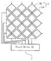
- the touch screen panel of FIG. 2includes a linear sensor pattern 5a in the horizontal direction, a linear sensor pattern 5b in the longitudinal direction, and a touch drive IC 7 for analyzing a touch signal.
- the touch screen paneldetects the magnitude of the capacitance formed between the linear sensor pattern 5 and the finger 8, and scans the linear sensor pattern 5a in the horizontal direction and the linear sensor pattern 5b in the longitudinal direction. By detecting the signal, a plurality of touch points can be recognized.
- the touch screen panel as described aboveis mounted and used on a display device such as an LCD, a phenomenon in which signal detection is difficult due to noise occurs.
- the LCDuses a common electrode, and in some cases, an AC common voltage Vcom is applied to the common electrode.
- the common voltage Vcom of the common electrodeacts as noise when detecting the touch point.
- the display device 200has a structure in which a liquid crystal is sealed between the lower TFT substrate 205 and the upper color filter 215 to form the liquid crystal layer 210.
- the TFT substrate 205 and the color filter 215are bonded by the sealant 230 at the outer portion thereof.
- polarizersare attached to the upper and lower sides of the liquid crystal panel, and optical sheets such as a BLU (Back Light Unit) and a Brightness Enhancement Film (BEF) are installed.
- BLUBack Light Unit
- BEFBrightness Enhancement Film
- a touch screen panelis installed on the display device 200 as shown.
- the touch screen panelhas a structure in which the linear sensor pattern 5 is mounted on the upper surface of the substrate 1.
- a protective panel 3 for protecting the linear sensor pattern 5is attached on the substrate 1.
- the touch screen panelis attached to an edge portion of the display device 200 through an adhesive member 9 such as a double adhesive tape (DAT), and forms an air gap 9a between the display device 200.
- DATdouble adhesive tape
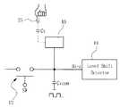
- a capacitance such as Ctis formed between the finger 8 and the linear sensor pattern 5.
- a capacitance such as Cvcomis formed between the linear sensor pattern 5 and the common electrode 220 formed on the lower surface of the color filter 215 of the display device 200, and the linear sensor pattern 5 has a capacitance.
- Cpan unknown parasitic capacitance, is also working.
- a circuitsuch as the equivalent circuit of FIG. 4 is configured.
- the conventional touch screen paneldetects a touch by detecting a change amount of Ct, and background components such as Cvcom and Cp act as noise in detecting Ct.
- background componentssuch as Cvcom and Cp act as noise in detecting Ct.
- the common voltage Vcom of the common electrode 220since the common voltage Vcom of the common electrode 220 alternates by one or a plurality of gate lines as shown in FIG. It acts as a significant noise during touch detection.
- an air gap 9ais disposed between the touch screen panel and the display device 200 as shown in FIG. 3.
- a shielding layeris formed by applying ITO or the like to the lower surface of the substrate 1 of the touch screen panel, and the shielding layer is grounded with the ground signal.
- the thickness of the productis increased by the air gap 9a and quality deterioration occurs.
- the prior artrequires a separate process for constituting the shielding layer, causing an increase in manufacturing cost.
- the touch screen panelis embedded in the LCD, it is impossible to form the air gap 9a or the shielding layer, and thus it is impossible to manufacture the touch screen panel in the LCD or the like.
- the present inventionis proposed to solve the problems of the conventional capacitive touch screen panel as described above, and minimizes the influence of external noise, the parasitic capacitance, and the influence of the common electrode of the display device.
- the present inventionprovides a touch detection device and method of a novel method that is easy to detect a touch signal and at the same time easy to incorporate a touch screen panel in a display device such as LCD, and a display device incorporating the touch detection device.
- a capacitive touch detection apparatuscomprising: a sensor pattern forming a touch capacitance Ct between a touch input tool and spaced apart from a common electrode to form a common electrode capacitance Cvcom; Charging means for supplying a charging signal to the sensor pattern to accumulate charge in the common electrode capacitance (Cvcom); And a level shift detection unit connected to the sensor pattern and detecting a level shift occurring in the voltage variation in the sensor pattern at the time of touch generation with respect to the voltage variation in the sensor pattern when the touch is not generated.
- the common electrodehas a common voltage Vcom level alternated at a predetermined frequency
- the level shift detection unitperforms a level shift between voltage variations generated in the sensor pattern by the common voltage Vcom before and after a touch occurs. Detect.
- Equation 1When the touch is not generated, the voltage variation is determined by Equation 1 below, and when the touch capacitance Ct is added, the voltage variation is determined by Equation 2 below, and the level shift is represented by Equation 1.
- Equation 2Is the difference between the voltage fluctuations of ⁇ Equation 2>.
- Is the voltage variation in the sensor patternIs the high level voltage of the common electrode, Is the low level voltage of the common electrode, Is the common electrode capacitance, Is the parasitic capacitance, Is the touch capacitance.
- the level shift detection unitdetects a level shift in the sensor pattern at a rising time and / or a falling time of the common voltage level.
- the level shift detectormay detect a touch occupancy rate of the touch input tool with respect to the sensor pattern based on the magnitude of the level shift.
- the level shift detectormay include a differential amplifier for differentially amplifying a signal in the sensor pattern.
- the touch detection methodmay further include a common voltage applying unit configured to apply the common voltage to the common electrode.
- the touch detection methodcomprises the steps of: supplying a charging signal to the sensor pattern and the common electrode capacitance (Cvcom) formed in the sensor pattern; Stopping the supply of the charge signal and isolating charge of the charge signal; Detecting a voltage variation in the sensor pattern by a common voltage Vcom applied to the common electrode capacitance Cvcom; And detecting a level shift between the voltage fluctuations before and after the touch occurs to obtain a touch signal.
- Cvcomcommon electrode capacitance
- the touch detection methodmay further include differentially amplifying a signal in the sensor pattern.
- the differential input signalmay be the voltage change when no touch occurs.
- the touch detection methodmay further include storing the voltage variation when the touch is not generated in the memory for each sensor pattern.
- a display device having a capacitive touch deviceincludes a touch capacitance (Ct) between the touch input tool, and is spaced apart from the common electrode to form the common electrode capacitance (Cvcom).
- Cttouch capacitance
- Cvcomcommon electrode capacitance
- Charging meansfor supplying a charging signal to the sensor pattern to accumulate charge in the common electrode capacitance (Cvcom);
- a level shift detection unitconnected to the sensor pattern and detecting a level shift occurring in the voltage variation in the sensor pattern at the time of touch generation with respect to the voltage variation in the sensor pattern when the touch is not generated.
- the common electrodehas a common voltage Vcom level alternated at a predetermined frequency
- the level shift detection unitperforms a level shift between voltage variations generated in the sensor pattern by the common voltage Vcom before and after a touch occurs. Can be detected.
- the capacitive touch device of the display devicemay further include a common voltage receiver configured to receive common voltage information of the common electrode.
- the capacitive touch device of the display devicemay further include a common voltage detector configured to detect a common voltage level of the common electrode.
- the charging means and the level shift detectormay be installed in the invisible region of the display device.
- the capacitive touch detection devicethe detection method and the touch screen panel using the level shift of the present invention, and the display device incorporating such a capacitive touch screen panel, it is possible to reduce the vertical noise, coupling phenomenon and other factors from the display device. By the parasitic capacitance generated by the effect is minimized and the signal misrecognition is not generated.
- the touch resolutionis increased and fine writing and drawing are possible.
- the active area of the touch panelcan be configured as a single layer, the manufacturing process is simplified and the yield is good.
- FIG. 1is a perspective view showing an example of a conventional capacitive touch screen panel
- FIG. 2is a plan view showing another example of a conventional capacitive touch screen panel
- FIG. 3is a cross-sectional view illustrating an example in which the touch screen panel of FIG. 2 is installed on a display device.
- FIG. 4is an equivalent circuit diagram of detecting a touch capacitance in FIG. 3.
- FIG. 5is a waveform diagram illustrating a common voltage waveform of a liquid crystal display device
- FIG. 6is a circuit diagram illustrating a touch detection device according to the present invention.
- FIG. 7Ais a cross-sectional view of a touch screen panel according to an embodiment of the present invention.
- FIG. 7Bis a cross-sectional view of a touch screen panel and a display device according to an embodiment of the present invention.
- FIG. 8is a circuit diagram illustrating an example of a touch detection apparatus
- FIG. 9is a waveform diagram illustrating a process of detecting a touch signal in the embodiment of FIG. 8;
- 11A and 11Bare circuit diagrams illustrating another example of the touch detection apparatus.
- FIG. 13is a block diagram showing an example of the configuration of a memory unit
- 14Ais a block diagram showing an embodiment of a touch screen panel
- 14Bis a block diagram showing an embodiment of a touch screen panel
- 15A to 15Dare circuit diagrams showing an embodiment of a signal processing unit
- 16is a configuration diagram showing another embodiment of the touch screen panel
- 17 to 19are configuration diagrams sequentially showing an example of configuring the sensor pattern in a plurality of layers
- FIG. 21is a diagram illustrating an example of minimizing coupling in the embodiment of FIG. 20.
- FIG. 22is a diagram illustrating another example of minimizing coupling in the embodiment of FIG. 20.
- FIG. 23is a plan view showing an example in which a plurality of drive ICs are installed
- 24is a configuration diagram showing another embodiment of the touch screen panel
- 25is a cross-sectional view showing an example of installation of the touch screen panel.
- 26is a cross-sectional view showing another example of installation of the touch screen panel.
- FIG. 27is a cross-sectional view of a display device having a touch screen panel according to the present invention.
- FIG. 28is an exploded perspective view illustrating the embodiment of FIG. 26.
- the present inventionrelates to a capacitive touch detection device using a level shift, a detection method and a touch screen panel, and a display device incorporating such a capacitive touch screen panel.
- a common electrode having an alternating voltageis formed, and a voltage change generated by the mutual relationship between the common electrode and the sensor pattern is detected.
- the touch detection systemcompares the voltage variation due to the common electrode capacitance between the common electrode and the sensor pattern when no touch occurs, and the voltage variation when the touch capacitance is added to the common electrode capacitance due to touch generation.
- a level shiftwhich is a magnitude difference between two voltage variations, the influence of noise or parasitic capacitance generated in the display device is minimized, and a touch signal can be obtained more stably.
- the present inventiondetects a non-contact touch input of a touch input tool having a finger or similar electrical characteristics.
- non-contact touch inputmeans that a touch input tool such as a finger makes a touch input while being spaced apart from the sensor pattern by a substrate at a predetermined distance.
- the touch input toolmay contact the outer surface of the substrate.
- the touch input tool and the sensor patternremain in a non-contact state. Therefore, the touch action of the finger on the sensor pattern may be expressed by the term "access”.
- the fingersince the finger may be in contact with the outer surface of the substrate, the touch action of the finger against the substrate may be expressed by the term "contact”.
- "access” and “contact”are commonly used as the meaning above.
- components described beloware components that perform certain roles, and refer to software or hardware components such as a field-programmable gate array (FPGA) or an application specific integrated circuit (ASIC).
- ⁇ partis not meant to be limited to software or hardware.
- ⁇may be configured in an addressable storage medium or may be configured to play one or more processors.
- ⁇ partmay include certain processes, functions, properties, subroutines, segments of program code, firmware, microcode, database, variables.
- “ ⁇ part”may be included in larger component or “ ⁇ part” or may include smaller components and “ ⁇ part”.
- the " ⁇ part”may have its own CPU.
- FIG. 7Ais a cross-sectional view illustrating a basic configuration of a touch screen panel in which a common electrode is formed according to an exemplary embodiment of the present invention.
- FIG. 7Bis a cross-sectional view illustrating a configuration of a touch screen panel and a display device in which a common electrode is formed in the display device according to an exemplary embodiment of the present invention.
- the touch detection apparatus of the present inventionbasically includes a sensor pattern 10, a common electrode 20, a charging means 12, and a level shift detector 14.
- the sensor pattern 10is a patterned electrode for detecting a touch input, and forms a touch capacitance Ct between a touch input tool such as a finger 25 of the body or a similar conductor.
- the sensor pattern 10is formed of a transparent conductor when the touch screen panel is placed on the display device.
- the sensor pattern 10may be formed of a transparent material such as indium tin oxide (ITO), antimony tin oxide (ATO), carbon nano tube (CNT), indium zinc oxide (IZO), or a transparent material having similar conductivity characteristics. do. If a touch screen panel such as a touch keyboard or a touch pad is not on the display device, the sensor pattern 10 may be formed of metal.
- the sensor pattern 10may be patterned in various forms.
- the islands isolated in the active region of the substrate 50may be in the form of a dot matrix in which the islands are arranged in a matrix, or linear patterns may be arranged to cross the substrate 50.
- the shape of the sensor pattern 10will be described in the following embodiments.
- the common electrodeis an electrode spaced apart from the sensor pattern 10. As shown in FIG. 7A, the common electrode 20 may be formed on the touch screen panel, and as shown in FIG. 7B, the common electrode of the display device of the common electrode 220 may be used.
- the sensor pattern 10is formed on the top surface of the substrate 50.
- the common electrode 20may be formed on the bottom surface of the 50.
- the common electrode 20may be formed over the entire lower surface of the substrate 50.
- the common electrode 20 in the embodiment shown in Figure 7ais used to detect the level shift to be described later, it is not necessarily physically formed on the touch panel screen, it is equivalent to the circuit shown in Figure 6 It can be formed at any position.
- the common electrode 20may be formed in the driving IC to form Cvcom with each dot matrix sensor pattern 10.
- the common voltage 20is applied to the common electrode 20 alternately at a predetermined frequency.
- a conductor such as a finger 25approaches the sensor pattern 10
- a common electrode capacitance Cvcomis formed between the sensor pattern 10 and the common electrode 20, and the common electrode capacitance is formed by the charged voltage.
- Cvcomhas a predetermined voltage level.
- the sensor pattern 10which is the other end of the common electrode capacitance Cvcom, is alternating by an alternating electric field applied to the common electrode 20.
- the potential ofwill fluctuate. That is, the potential of the sensor pattern 10 varies in voltage by the common electrode capacitance Cvcom.
- Ct and Cvcom and the likeare symbols representing the name and size of the capacitor at the same time.
- Ctmeans a capacitor having the name Ct and a capacitance of the size Ct.
- the display device 200has a common electrode 220.
- the display device 200may be the aforementioned various types of display devices, and the common electrode 220 may be a Vcom electrode of the LCD or another type of electrode. 7 illustrates an LCD among display devices.
- the display device 200 illustrated in FIG. 7Bhas a structure in which a liquid crystal is sealed between the lower TFT substrate 205 and the upper color filter 215 to form the liquid crystal layer 210.
- the TFT substrate 205 and the color filter 215are bonded by the sealant 230 at the outer portion thereof.
- polarizersare attached to the upper and lower sides of the liquid crystal panel, and optical sheets such as a BLU (Back Light Unit) and a Brightness Enhancement Film (BEF) are installed.
- BLUBack Light Unit
- BEFBrightness Enhancement Film
- a substrate 50 of the touch screen panelis installed on the display device 200.
- the substrate 50is attached to the upper portion of the display device 200 through an adhesive member 57 such as a double adhesive tape (DAT) at an outer portion thereof.
- An air gap 58is formed between the substrate 50 and the display device 200.
- the level shiftcan be detected according to the embodiment of the present invention.
- the charging means 12is a means for selectively supplying a charging signal to the sensor pattern 10 when necessary.
- the charging means 12is a three-terminal switching element that performs a switching operation according to a control signal supplied to the on / off control terminal, or a linear element such as an OP-AMP that supplies a signal according to the control signal.
- the charging means 12may include a relay, a metal oxide semiconductor (MOS) switch, a bipolar junction transistor (BJT), a field effect transistor (FET), a metal oxide semiconductor field effect transistor (MOSFET), and an insulated gate bipolar (IGBT). Transistor) and TFT (Thin Film Transistor).
- a relayis a device that outputs a voltage or current applied to an input terminal without loss when a current is applied to a control terminal
- a BJTis a base terminal in a state in which a voltage higher than a threshold voltage of the base is applied to the base.
- TFTis a switching device used in pixel parts such as LCD and AMOLED, and is composed of gate terminal as control terminal, drain terminal as input / output terminal, and source terminal, and gate terminal as source terminal.
- a current flowing through the input terminal to the output terminal while conductingis dependent on the magnitude of the voltage applied to the gate terminal.
- various elementssuch as OP-AMP or flip-flop having Enable and Disable terminals may be used.
- Ct and Cvcom acting on the sensor pattern 10are connected to the output terminal of the charging means 12. Therefore, Ct and Cvcom are charged when a charging signal such as an arbitrary voltage or current is applied to the input terminal while the charging means 12 is turned on. At this time, the parasitic capacitance Cp (Parastic Capacitance), which is not shown, will also be charged.
- CpPara Capacitance
- the input terminal of the level shift detector 14has a high impedance (Hi-impedance or Hi-z). If the touch input is observed while discharging the signals charged in Ct and Cvcom, the charging signal is isolated by other means, or the signal is quickly observed at the start of discharge, the input terminal of the level shift detection unit 14 must be Hi-. It does not have to be z.
- the level shift detection unit 14detects whether the signal level in the sensor pattern 10 is shifted. Preferably, the level shift detection unit 14 adds Ct in parallel to the generation of the touch (that is, Cvcom) in preparation for the voltage variation in the sensor pattern 10 when the touch is not generated (that is, when no Ct is formed). The touch signal is detected by detecting whether a level shift occurs in the voltage variation in the sensor pattern 10.
- the level shift detector 14may have various elements or circuit configurations. In the following embodiment, an example in which a switching element and a differential amplifier are used as the level shift detection unit 14 will be described. However, the configuration of the level shift detection unit 14 is not limited to such an embodiment.
- a touch capacitance Ctis formed between the finger 25 and the sensor pattern 10
- the common electrode capacitance Cvcomis between the sensor pattern 10 and the common electrodes 20 and 220.
- the hidden lineis a flat layer 24 for protecting the sensor pattern 10. If a protective panel such as tempered glass is attached to the upper surface of the substrate 50, the flat layer 24 may be formed as described above. Can be removed
- Is the voltage variation in the sensor pattern 10Is the high level voltage of the common electrode 20, Is the low level voltage of the common electrode 20, Is the common electrode capacitance, Is the parasitic capacitance, Is the touch capacitance.
- the level shift detection unit 14detects the level shift in the sensor pattern 10 by using Equation 1 and Equation 2 as described above.
- VcomH and VcomLare easily set values.
- Cvcomcan be obtained from Equation 3 below.
- Equation 3it can be obtained from the permittivity of the silver substrate 50.
- the relative dielectric constantis 3 to 5, so that the dielectric constant of the substrate 50 can be obtained by multiplying the dielectric constant of the vacuum.
- S1may be easily obtained since the area of the sensor pattern 10 and the common electrode 20 are opposite to each other.
- the common electrodeis formed over the entire lower surface of the substrate 50 as in the example of FIGS. 7A and 7B, the opposing area S1 is determined by the area of the sensor pattern 10.
- D1is the distance between the sensor pattern 10 and the common electrode 20, it corresponds to the thickness of the substrate 50.
- Cvcomis a value that can be easily obtained and set.
- ⁇can be obtained from the medium between the sensor pattern 10 and the finger 25. If the glass is attached to the upper surface of the substrate 50 in Figure 7, the dielectric constant ⁇ can be obtained from the product of the dielectric constant of the vacuum by the relative dielectric constant of the glass.
- S2corresponds to the opposing area of the sensor pattern 10 and the finger 25. If the finger 25 covers all of the sensor patterns 10, S2 corresponds to the area of the sensor pattern 10. If the finger 25 covers a part of the sensor pattern 10, S2 will be reduced by an area not facing the finger 25. In addition, since D2 is the distance between the sensor pattern 10 and the finger 25, it will correspond to the thickness of the tempered glass or the flat layer 24, etc. placed on the upper surface of the substrate 50.
- Ctis also a value that can be easily obtained, and can be easily set using a protection panel or a flat layer 24 placed on the substrate 50.
- Ctis proportional to the opposing areas of the finger 25 and the sensor pattern 10
- the touch occupancy ratio of the finger 25 with respect to the sensor pattern 10can be calculated from this.
- the level shift detection unit 14detects whether or not a level shift has occurred in the voltage change caused by Equation 2 in preparation for the voltage change caused by Equation 1 above.
- the level shift detector 14may include an amplifier for amplifying a signal in the sensor pattern 10, an analog to digital converter (ADC), a voltage to frequency converter (VFC), flip-flops, latches, and buffers. (Buffer), TR (Transistor), Thin Film Transistor (TFT), Comparator, or the like, or a combination of these components.
- the level shift detector 14includes a signal detection switching element 16.
- the signal detection switching element 16is a TFT as an example. Referring to FIG. 8, the on / off control terminal of the signal detection switching element 16 is connected to the sensor pattern 10. Therefore, the current i flowing through the input / output terminal of the signal detection switching element 16 is controlled by the potential in the sensor pattern 10. As shown, if the connection point of the on / off control terminal of the sensor pattern 10 and the signal detection switching element 16 is " P1 ", the potential V_P1 at P1 is as shown in ⁇ Equation 1 > Affected by Cvcom and Ct.
- V_P1has a voltage variation as shown in ⁇ Equation 1>. If a touch input occurs, Ct is added in parallel to Cvcom. The voltage fluctuations are level shifted towards decreasing.
- FIG. 9is a waveform diagram illustrating a process of detecting a touch signal in the embodiment of FIG. 8. A method of detecting a touch signal using level shift will now be described with reference to this.
- Cvcomis charged by turning on the charging means 12 and supplying a charging signal Vb. If the charging means 12 is turned off, the charge stored in the Cvcom remains in an isolated state because the gate input terminal of the signal detection switching element 16 is always in the Hi-z state. Accordingly, the potential of the sensor pattern 10 is also maintained.
- the On voltage of the charging means 12is 15V and the Off voltage is -8V. If the on / off voltage applied to the gate is set to a sufficient difference, more stable on / off characteristics can be obtained.
- the charging signal Vbis applied at 5V, and is synchronized with the gate signal Vg to be 0V when the gate is off, or maintains a potential difference of 5V or more relative to the gate voltage so that the voltage applied to the gate maintains a sufficient turn-off state.
- the common voltage of the common electrode 20is given as 4V at the Hi level and -1V at the Low level. As illustrated, after the charging operation is performed first, the detection operation is performed at the rising time and the falling time of the common voltage. However, the charging operation and the detection operation are not necessarily performed sequentially.
- the gate off period of the charging means 12may be shortened to allow the Cvcom to always be in a charged state, or the Cvcom may be maintained in a charged state by completely blocking other discharge paths.
- the charging operationwill not necessarily need to be performed before such a detection operation. By this operation, the current consumption can be reduced.
- the detection operationmay be performed only in the rising section of the common voltage or in the falling section. Alternatively, the detection operation may be performed every few periods of the common voltage.
- the detection 1 operationis performed in the falling section of the common voltage.
- the detection 1 operationis performed immediately after the drop of the common voltage or after a predetermined time has elapsed.
- a voltage variation as shown in Equation 1occurs. If it is assumed that Cp is negligibly small compared to Cvcom, it is the falling section of common voltage. The value of is "- ⁇ 4-(-1) ⁇ * 1 " Therefore, the potential V_P1 of P1 varies from 5V to 0V.
- the current flowing in the input / output terminal of the signal detection switching element 16drops in conjunction with the potential of P1 as shown in the waveform diagram of FIG.
- a TFTis used as the signal detection switching element 16
- a high current fluctuation valuecan be obtained in comparison with the fluctuation of the gate voltage.
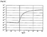
- 10is a graph showing the characteristics of the output current versus the gate voltage of the TFT. Referring to this, when the gate stage voltage is 5V and 0V, the difference in output current is approximately 1,000 times. Therefore, it is very easy to read the voltage variation of P1.
- a comparatoris added to the input terminal of the signal detection switching element 16 in parallel or at the output terminal, and a signal corresponding to the voltage level at P1 when no touch occurs as a reference signal of the comparator is applied, the level shift at P1 when the touch occurs. May be more easily detected.
- Ct formed between the finger 25 and the sensor pattern 10acts.
- Ctcan be designed under various conditions. If the distance between the finger 25 and the sensor pattern 10 and the dielectric constant of the medium, the distance between the sensor pattern 10 and the common electrode 20 and the dielectric constant of the medium are the same, the finger 25 is the sensor pattern 10 If it covers the whole, Cvcom and Ct have the same value. Therefore, the voltage fluctuation at P1 by ⁇ Equation 2> because it is the rising section of common voltage Since the value of " ⁇ 4-(-1) ⁇ * 1/2" is 2.5V. Therefore, the potential V_P1 of P1 varies from 5V to 7.5V. The current flowing in the input / output terminal of the signal detection switching element 16 rises in conjunction with the potential of P1 as shown in the waveform diagram of FIG.
- the charging 3 operationis performed again, and detection 3 detects the level shift in the falling section of the common voltage.
- V_P1falls to 0V
- V_P1falls to 2.5V. That is, when the touch input is generated, the signal at V_P1 is level shifted downward in the rising section of the common voltage, and level shifted upward in the falling section of the common voltage.
- FIG. 11A and 11Bare circuit diagrams illustrating another example of the touch detection apparatus, and show another example of the level shift detection unit 14.
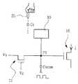
- the level shift detector 14includes an amplifier 18 having an input terminal connected to the sensor pattern 10. Since the amplifier 18 also has Hi-z input, it can stably isolate the signal at P1.
- the voltage variation of P1is changed by Cvcom and Ct as in the embodiment of FIG. 8.
- the amplifier 18is used as a means for detecting the level shift.
- the amplifier 18amplifies the signal in the sensor pattern 10. Accordingly, since the magnitude of the level shift due to the touch is amplified and output, the touch signal can be stably obtained.
- FIG. 11Bshows an example in which a differential amplifier 18a is used as the amplifier 18.
- the differential amplifier 18adifferentially amplifies the signal in the sensor pattern 10 in accordance with the inverted or non-inverted differential input voltage Vdif.
- Vdifis externally adjustable.
- Vdifmay be a signal corresponding to a charging signal applied through the charging means 12.
- Vdifis a signal corresponding to the voltage level at P1 when no touch occurs.
- Vdifmay be 10V in a period in which the common voltage is high, and 0V in a low period.
- Vdifcorresponds to the voltage level at P1 when no touch occurs
- the differential amplifier 18awill amplify and output only the level shift value at the time of touch generation. Therefore, a cleaner and more stable touch signal can be obtained.
- Vdifit is necessary to extract the voltage level at P1 when no touch occurs. Also, in order to obtain a touch signal in each of the rising and falling sections of the common voltage level, Vdif must also separately extract the voltage level of P1 when no touch occurs in each of the rising and falling sections of the common voltage level.
- the Vdifmay be determined and input at the stage of manufacturing the touch screen panel. In addition, the voltage level of P1 may be detected at initial power-on or periodically when no touch occurs.
- FIG. 12is a waveform diagram illustrating a process of detecting a touch signal in the embodiment of FIG. 11B. Referring to this, an example of signal detection when the differential amplifier 18a is used as the level shift detection unit 14 will be described.
- the On voltage of the gate voltage Vg of the charging means 12is 3V, and the Off voltage is 0V.
- the charging signal Vbis applied at 5V.
- the common voltage of the common electrode 20is given at 3V at the Hi level and 0V at the Low level.
- the detection operationis performed after the charging operation.
- Cvcom and Ctare assumed to be the same, and Cp is assumed to be a negligible value. In describing the exemplary embodiment of FIG. 12, detailed descriptions of parts identical to those described in FIG. 9 will be omitted.
- V_P1 of P1When charging 1 is performed, the potential V_P1 of P1 is maintained at 5V, which is the charging voltage.
- the detection 1 operationis performed in the rising section of Vcom after charging 1. The detection 1 operation occurs immediately after the rise of Vcom or after a predetermined time elapses. Since touch is not generated, ⁇ Equation 1> The value of is "(3-0) * 1", that is, 3V. Therefore, V_P1 rises to 8V. Since no touch occurs, Vdif is also given at 8V. When no touch occurs, the voltage level of V_P1 and Vdif are ideally the same, so that the output Vt of the differential amplifier 18a hardly occurs. Even if there is an influence due to noise or the like, Vt is output as a very weak signal.
- the touch input at this timeis performed by the finger 25 with the entire sensor pattern 10. Suppose you cover the whole area.
- V_P1fluctuates by "-(3-0) * 1/2" according to ⁇ Equation 2>. That is, it can be seen that V_P1 is 3.5V in detection 2, and a level shift of 1.5V has occurred compared to when no touch occurs.
- Vdif of the differential amplifier 18acorresponds to the value of V_P1 when no touch occurs, it varies by "-(3-0) * 1" according to ⁇ Equation 1> and has a value of 2V.
- the output Vt of the differential amplifier 18aamplifies and outputs 1.5V, which is the difference between the two inputs, V_P1 and Vdif.
- the 1.5V level-shift voltage valueis easily recognizable even at low amplification rates.
- the amplification factor of the differential amplifier 18acan be appropriately selected to obtain a high Vt value during touch input.
- V_P1After detection 2, charging 3 proceeds again, and V_P1 returns to 5V.
- V_P1since a touch input occurs in the rising section of Vcom, V_P1 varies by ((3-0) * 1/2) according to ⁇ Equation 2>. That is, V_P1 is 6.5V, and a level shift of -1.5V is issued compared to when no touch occurs. Therefore, as in detection 2, V_P1 of 6.5V is differentially amplified based on Vdif of 8V to obtain Vt, and a touch signal is obtained therefrom.
- V_P1When the operation of charge 4 is performed, V_P1 returns to 5V again. Then, the detection 4 detects the touch input. At this time, since the finger 25 occupies as much as 1/2 the area of the sensor pattern 10, the facing area is expressed by Equation 4. Decreases by 1/2. Therefore, Ct has a value of "Cvcom * 1/2". Substituting this in ⁇ Equation 2>, the detection 4 Is "-(3-0) * 1 / 1.5". Thus, as shown, V_P1 has 3V. This means that 1V level shift occurs compared to 2V without touch, and the differential amplifier amplifies 1V differentially.
- V_P1 and Vdifare equally ideal. Therefore, only a weak signal corresponding to noise is outputted in Vt.
- V_P1is level shifted by 1.5V or -1.5V.
- V_P1is level shifted by 1V or -1V. That is, the touch signal can be obtained by detecting the level shift from the output of the differential amplifier 18a, and the touch occupancy rate of the touch input tool having the finger 25 or similar conductive characteristics can be calculated very easily.
- the charging signal Vbis applied at 5V in the on period of the charging means 12.
- the charging signal Vbmay be provided at two voltage levels instead of a single voltage level.
- Vbis supplied at 8V before the falling section of the common voltage Vcom
- Vbis supplied at 2V before the rising section of Vcom.
- V_P1can be maintained at a constant voltage regardless of the rising and falling sections of Vcom when touch is not generated, thus helping to keep the manufacturing IC voltage low.
- the falling section of Vcomit is 5V when -3V fluctuates compared to the charging voltage of 8V
- the rising section of Vcomit is 5V when 3V fluctuates compared to the charging voltage of 2V.
- V_P1is 5V
- touchoccurs
- Cpis assumed to be a negligible value in comparison with Cvcom in Equations 1 and 2.
- the sensor pattern 10 and the common electrode 20are formed on both surfaces of the substrate 50, external noise and parasitic capacitance Cp are relatively very small.
- the parasitic capacitance (Cp)can act largely.
- Cvcom, Ct, and Cpare all 1pF, when the height difference of common voltage (Vcom) is 3V, when no touch occurs Is "3 * 1/2" and when touch occurs Is "3 * 1/3".
- Vcomcommon voltage
- 500mVis a value that can be detected very easily through the differential amplifier 18a, and since the ratio of Cp is higher, the value can be easily recognized even when the magnitude of the level shift is several tens of mV.
- Cpmay be different for each sensor pattern 10. For example, it is very difficult to design the position of the sensor pattern 10, the wire length, other external factors, and the like uniformly for every sensor pattern 10.
- Cvcommay also be different for each sensor pattern 10. If the magnitude of the level shift is large, such a deviation can be ignored, but the smaller the magnitude of the level shift is, the less the value of each deviation of the sensor pattern 10 becomes.
- the drive IC 30has a memory unit for storing the output signal of the differential amplifier 18a when a touch does not occur for each sensor pattern 10 as shown in FIG. 28) may be further included.
- the output signal of the differential amplifier 18a stored in the memory unit 28is a value based on the inherent Cp of each sensor pattern 10 and may be different for each sensor pattern 10.
- the output of the differential amplifier 18amay be obtained in a state where no touch occurs. If the output deviation of the differential amplifier 18a is large for each sensor pattern 10, the output of the differential amplifier 18a when the touch is not generated may be disregarded again.
- the differential amplifier 18a output in the non-touch state at the factory shipment stagemay be stored in the memory unit 28 for each sensor pattern 10.
- the memory unit 28may be additionally installed to store a value when a touch occurs.
- the drive IC 30may compare the values of the same cell to determine that a touch has occurred when a change occurs over a preset reference value.
- the memory unit 28is composed of a table having m rows and n columns.
- the M1-1 addressstores the output of the differential amplifier 18a when no touch is allocated to the sensor pattern 10 at the upper left.
- the signal stored in the memory unit 28is referred to when detecting whether the sensor pattern 10 is touched at the upper left end.
- Values stored at respective addresses of the memory unit 28may be periodically corrected. Periodic calibration may be performed when powering the device as above, or in a dormant state. In this way, the output of the differential amplifier 18a is stored in the memory unit 28 when the touch is not generated (or separately when the touch is not generated and when it is generated) for each sensor pattern 10, periodically corrected, and the memory is detected when the touch signal is detected. Referring to the unit 28, the touch signal may be stably obtained even when the sensor pattern 10 has a unique Cp.
- FIG. 14A to 24illustrate embodiments of a touch screen panel according to the present invention.
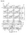
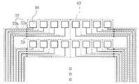
- FIG. 14Aillustrates an example in which the above-described touch detection apparatus is applied, and the sensor pattern 10 is arranged in a dot matrix form.
- the sensor patterns 10are arranged in a dot matrix form, and each sensor pattern 10 is provided with a charging means 12 and a signal detection switching element 16.
- the sensor pattern 10, the charging means 12, and the signal detection switching element 16form a unit cell.
- Such unit cellsare arranged in a matrix on glass, substrate, or other light transmissive substrate 50.
- the configuration as shown in Fig. 14Ais similar to that of the TFT substrate of the LCD.
- the substrate 50can be manufactured using the TFT substrate manufacturing process almost as it is in the LCD manufacturing process. This allows for ease of mass production, stable quality, low cost manufacturing and the like.
- the configuration of the drive IC 30is shown at the bottom of FIG. 14A.
- the drive IC 70includes a signal transmitting and receiving unit 31, a timing controller 33, a signal processor 35, an alternating voltage applying unit 37, and a memory unit 28.
- the detection signal acquired by the drive IC 30is transferred to the CPU 40.
- the CPU 40may be a CPU of a display device, a main CPU of a computer device, or a CPU of the touch screen panel itself.
- a touch processormay be processed by embedding a microprocessor such as 8bit or 16bit.
- the system configurationfurther includes a power supply unit for generating a high or low voltage of signals for detecting a touch input.
- the microprocessor built in the drive IC 30recognizes gestures such as zoom, rotation, and move by calculating touch input coordinates, and calculates reference coordinates (or center point coordinates) and gestures. Data can be transferred to the main CPU.
- gesturessuch as zoom, rotation, and move by calculating touch input coordinates, and calculates reference coordinates (or center point coordinates) and gestures. Data can be transferred to the main CPU.
- reference coordinatesor center point coordinates
- datacan be transferred to the main CPU.
- generating a zooming signalby calculating the area of the touch input, calculating the intensity of the touch input, or when a plurality of GUI objects are touched at the same time, only the GUI object desired by the user (for example, a large area detected) is valid. You can also process and export the data in a variety of forms, including recognizing it as input.
- the timing controller 33generates a time division signal of several tens of ms or less, and the signal processor 35 transmits and receives a signal to each sensor pattern 10 through the signal transmitter / receiver 71.
- the alternating voltage applying unit 37applies a voltage level alternated at a predetermined frequency to the common electrode 20 according to the time division signal of the timing controller 33.
- the frequency of the alternating voltage applied to the common electrode 20can be adjusted by adjusting a resistor.
- the signal transmission / reception unit 31supplies the on / off control signal Vgn of the charging means 12 and the charging signal Vbn. Further, the touch detection signal is transmitted and received from the input / output terminal of the signal detection switching element 16.
- the on / off control signal Vgnis time-divided by the timing control section 33 and is scanned and supplied for each line.
- the touch detection signal Snis supplied to the signal transmission / reception unit 31 at a rising time or a falling time of the common voltage Vcom after Vbn is supplied to perform a charging operation in each sensor pattern 10. do. As described above, Sn may be generated in each of the rising and falling sections of Vcom.
- the memory unit 28is used to correct signals when no touch occurs in each sensor pattern 10 or to store signals when touch occurs. 10) Each has its own absolute address. Each absolute address stores reference values for correcting the sensor patterns 10 (or a value detected when touched with the reference value).
- the memory 28may temporarily store the coordinate values obtained with only one, or may store the reference value when no touch occurs.
- the plurality of memory meansmay be configured to separately store a reference value when no touch occurs and a detection value when a touch occurs.
- the illustrated embodimentexemplifies a case where the sensor pattern 10 has a resolution of 3 * 3, since the sensor pattern 10 actually has a higher resolution, a signal may be lost in the process of processing many signals. For example, when the signal processor 35 is in the "Busy" state, the signal may not be recognized because the touch detection signal is not recognized. The memory unit 28 prevents such a loss of the signal.
- the signal processor 35detects a touch signal and temporarily stores the touch signal in the memory unit 28. After scanning the entire active area 90, the memory unit 28 is referred to to determine whether there is a missing signal. If there is a touch coordinate stored in the memory unit 28 but omitted in the signal processing, the signal processor 35 processes the touch coordinate as a normal input and erases the memory unit 28 before the next scanning.
- the embodiment illustrated in FIG. 14Amay be used when the common electrode 20 is formed on the touch screen panel to apply a common voltage.
- the common electrode 20may not be physically formed on the touch panel as long as it can satisfy the equivalent circuit of FIG. 6.
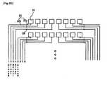
- FIG. 14Billustrates a touch detection device according to another embodiment of the present invention.
- an operation of receiving or detecting and using a common voltage from a display device and an operation of applying a common voltage to the common electrode 220may be performed by the display device.
- the drive IC 30may further include any one of a common voltage detector 43, a common voltage receiver 45, and an alternating voltage applying unit 37.
- the drive IC 30includes a common voltage detector 43, a common voltage receiver 45, and an alternating voltage applying unit 37 as shown in FIG. 14B, and the selector 47 controls the common voltage detector. 43, the common voltage receiver 45 or the alternating voltage applying unit 37 may be configured to be selected.
- 15A to 15Dillustrate embodiments of obtaining a touch signal from the signal processor 35.
- the level shift detector 14exemplifies that the signal detection switching device 16 is applied.
- a resistor Rnis connected to a source terminal, which is an output terminal of the signal detection switching element 16.
- the signal processor 35reads the current flowing through the resistor Rn at the source terminal of the signal detection switching element 16 or converts the resistor Rn and the current into a voltage to obtain a touch signal.
- the obtained touch signalis transmitted to the CPU 40.
- the signal processor 35detects a voltage formed by Rds (on), which is an on resistance of the signal detection switching device 16 when a current flows through the drain terminal of the signal detection switching device 16.
- the signal processor 35may include a voltage detector such as an ADC or a VFC, or may include a current detector such as a hall sensor.
- the signal processing unit 35may be configured by detecting a voltage or a current at a source terminal or a drain terminal of the signal detection switching device 16.
- the source or drain terminal of the signal detection switching device 16 to the drive IC 30are provided.
- the wiringbecomes long.
- Such long wiringincreases wiring resistance and increases coupling capacitor due to overlap between the wirings at the points where the wirings intersect. These resistances and coupling capacitances deteriorate the charge and discharge characteristics and thus act as a cause for delaying signals.
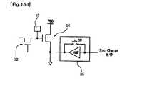
- FIG. 15C and 15Dshow an example in which the signal processing unit 35 includes a precharge circuit as a means for resolving signal delay due to resistance and coupling capacitance.
- an amplifier (Amp) or a switchis connected to the wiring connected to the drain terminal of the signal detection switching element 16, and the precharge voltage is transmitted to the drain terminal side through the wiring.
- the precharge voltageis 2V. Since the drain terminal is precharged to 2V before the touch signal is detected, high speed operation is performed without the above signal delay.
- the amplifier and the switchare shown as being connected in parallel, but they are installed individually one by one.
- FIG. 15Dshows an example in which a precharge circuit is installed at the source terminal of the signal detection switching element 16, and the operation method is the same as that of FIG. 15C.
- the signal processor 35needs to synchronize all signals to the change of the common voltage of the common electrode 220 in order to observe the waveform as shown in FIG. 9 or FIG. 12.
- the touch signalmay be obtained by relatively calculating the height of the detection signal relative to the charging voltage, reading the detection signal several times in succession, even if it is not necessarily synchronized with the change of the common voltage.
- the signal processor 35is configured to sink the charging signal, the detection signal, and the like to the change in the common voltage of the common electrode 220, so that the signal processing is stable.
- the signal processor 35detects common voltage information of the common electrode 220 of the display device 200, receives common voltage information from the display device 200, or uses the common electrode ( The common voltage alternately forced to 220 may be applied. In any case, the signal processor 35 may extract the starting point, magnitude, rising section, and falling section of the common voltage alternately at the common electrode 220, and process the signals accordingly.
- the drive IC 30includes at least one of the common voltage detector 43, the common voltage receiver 45, and the alternating voltage applying unit 37.
- the common voltage detector 43the common voltage detector 45
- the alternating voltage applying unit 37the common voltage applying unit 37.
- all three configurationsmay be provided, and any one may be selected and used by the selector 47.
- the common voltage receiver 45directly receives the common voltage information of the common electrode 220 from the display device 200.
- informationsuch as the start point, magnitude, rising section, and falling section of the common voltage can be obtained very easily, and the signal processing unit 35 can easily process signals in conjunction with the rising and falling sections of the common voltage.
- a burdenarises in that the display apparatus 200 needs to transmit common voltage information.
- the alternating voltage applying unit 37may apply the alternating voltage to the common electrode 220 by force. have.
- the alternating voltage applying unit 37applies a voltage level alternated at a predetermined frequency to the common electrode 220 according to the time division signal of the timing controller 33.
- the frequency of the alternating voltage applied to the common electrode 220can be adjusted by adjusting a resistor. Even in this case, the signal processor 35 can easily process the signal in association with the rising and falling sections of the common voltage. However, the burden of sending an oscillation signal to the display device 200 is generated.
- the common voltage detector 43automatically detects the common voltage information, it is not necessary to exchange information related to the common voltage with the display device.
- the common voltage detector 43is configured to detect that the potential of P1 is alternated according to the alternating of the common voltage in a state in which the charging means 12 cuts off the supply of the charging signal and electrically isolates the sensor pattern 10. do.
- the common voltage detector 43may have various circuit configurations, and a detailed embodiment will be described later.
- the charging means 12 and the signal detection switching element 16are installed in the unit cell.
- the charging means 12 and the signal detection switching element 16are constituted by TFTs
- the TFTsmainly use metal layers, there is a fear that the light is reflected and viewed.
- the TFTis formed of a transparent thin film or if it is not necessary to consider visibility such as a touch pad of a notebook, it does not matter.
- the touch screen panelis raised on the display device, the above visibility is a problem.
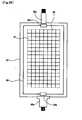
- FIG. 16shows an example of eliminating the visibility problem that may occur in the embodiment shown in FIGS. 14A and 14B.
- the sensor pattern 10is arranged in a dot matrix in the active region 90 of the substrate 50.
- a signal line 22is drawn out.
- the signal line 22is wired to the transparent signal line 22a at least in the active region 90.
- the charging means 12 and the signal detection switching element 16are integrated.
- the charging means 12 and the signal detection switching element 16are concealed by black ink or the like.
- the charging means 12 and the signal detection switching element 16are provided at a position apart from the sensor pattern 10, but the circuit configuration is the same as the embodiment of Fig. 14A or 14B.
- the charging means 12 and the signal detection switching element 16are formed by dividing at both edge portions of the substrate 50.
- Such a wiring structurecan shorten the longest wiring length of the transparent signal line 22a to lower the wiring resistance in the transparent signal line 22a and reduce the number of wirings of the transparent signal line 22a between the sensor patterns 10.
- the transparent signal line (22a)can also be wired in the longitudinal direction, the charging means 12 and the signal detection switching device 16 is distributed on the upper and lower edges of the substrate 50 It may be formed.
- the signal line 22may be wired to the metal signal line 22b.
- the transparent signal line 22a and the metal signal line 22bare formed in different layers, the transparent signal line 22a and the metal signal line 22b are connected to each other via a connection portion 59 formed through a process such as a contact hole.
- the transparent signal line 22ais formed of a transparent conductor having ITO, carbon nanotube (CNT), antimony tin oxide (ATO), indium zinc oxide (IZO), or the like.
- the thickness and width of the transparent signal line 22acan be appropriately selected to reduce the wiring resistance of the transparent signal line 22a as much as possible.
- the transparent signal line 22ahas a thickness of 50 to 200 ⁇ m and is formed to have a width of 10 to 100 ⁇ m.
- the metal signal line 22bis made of aluminum-based metal such as aluminum and aluminum alloy, silver-based metal such as silver and silver alloy, copper-based metal such as copper and copper alloy, molybdenum-based metal such as molybdenum and molybdenum alloy, chromium, titanium, Tantalum or the like.
- itmay include two films having different physical properties, that is, a lower film (not shown) and an upper film (not shown) thereon.
- the upper layeris made of a low resistivity metal such as aluminum (Al) or an aluminum alloy to reduce signal delay or voltage drop.
- the lower layermay be made of a material having excellent contact properties with indium tion oxide (ITO) and indium zinc oxide (IZO), such as molybdenum (Mo), molybdenum alloy, and chromium (Cr).
- ITOindium tion oxide
- IZOindium zinc oxide
- Momolybdenum
- Momolybdenum alloy
- Crchromium
- the black ink regiondoes not require the formation of a light blocking layer or the like on the upper surfaces of the TFTs.
- Simplificationcan reduce the number of photomasks, simplifying the manufacturing process.
- the condition for maintaining the gap between the transparent signal lines 22abecomes difficult and the physical touch resolution may be restricted.
- the following embodimentis an embodiment to solve the above limitations.
- FIGS. 17 to 19show an example in which the sensor pattern 10 and the transparent signal line 22a are formed in a plurality of layers in the active region 90.
- the sensor patterns 10when the sensor patterns 10 are formed in the plurality of layers, physical touch resolution may be increased, and the degree of freedom is increased in the wiring rules of the transparent signal lines 22a passing between the sensor patterns 10.
- the embodiment of FIGS. 17 to 19does not generate a point where the signal lines 22 intersect in the active region 90. Therefore, no coupling capacitance due to the intersection occurs, and there is no fair issue for insulation of the intersection.
- a process of forming the sensor pattern 10 using the plurality of layerswill be described with reference to FIGS. 17 through 19 as follows.
- a sensor pattern 10 and a transparent signal line 22aare formed in the active region 90 of the substrate 50 as shown in FIG.
- a transparent conductive materialsuch as ITO is applied onto the substrate 50 by a process such as sputtering or coating to form a conductive layer, which is exposed or etched by a photomask process to form a pattern as shown in FIG. 17.
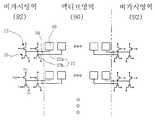
- the charging means 12 and the signal detection switching element 16are integrated in the invisible region 92.
- the wiring in the invisible region 92is formed as the metal signal line 22b in the process of forming the gate metal or the source metal.
- the sensor pattern 10 and the transparent signal line 22a as shown by a dotted line in FIG. 19are formed on the passivation layer.
- the transparent signal line 22a and the metal signal line 22bare connected by a process such as a contact hole.
- an additional protective filmmay be further formed to protect the top layer sensor pattern 10 during processing or transport.
- the sensor pattern 10 and the transparent signal line 22aare configured in multiple layers, the sensor pattern 10 may be arranged at a tight interval, and the upper layer may be disposed between the transparent signal lines 22a of the lower layer. Transparent signal lines 22a may be disposed. Therefore, the number of signal line wirings between the sensor patterns 10 can be increased, and the wiring rules of the transparent signal lines 65 can be freer in the same layer. Ultimately, the physical touch resolution may be increased even when applying the embodiment of FIG. 16 (or the embodiment of FIG. 20 to be described later).
- 20shows another embodiment of a touch screen panel. 20 illustrates an embodiment to which the touch detection apparatus of FIG. 11B is applied, and shows an example in which the sensor patterns 10 are arranged in a dot matrix form.
- the sensor pattern 10 and the signal line 22are formed in the active region 90 of the substrate 50.
- the signal line 22may be wired to the metal in the active region 90, but is preferably wired to the transparent signal line 22a in the active region 90.
- the signal line 22is wired to the transparent signal line 22a in the active region 90 and to the metal signal line 22b connected to the transparent signal line 22a and the connecting portion 59 in the invisible region 92. This is the same as the embodiment of FIG. In FIG. 20, however, the charging means 12 and the level shift detector 14 are provided in the drive IC 30.
- the level shift detector 14may be a switching device installed in the drive IC 30. However, as shown in the figure, when the differential amplifier 18a is used as the level shift detector 14, the touch signal is amplified and processed, so that the signal can be easily captured. Since the touch detection apparatus using the differential amplifier 18a has been described with reference to FIG. 11B, a detailed description thereof will be omitted.
- the sensor patterns 10are each drawn out as separate signal lines 22. Therefore, the drive IC 30 does not need to scan the sensor pattern 10 row by column.
- the drive IC 30may scan and supply a charging signal for each unit cell.
- the charging signalmay be scanned and supplied for every unit cell group that is grouped together.
- the charging signalsmay be scanned and supplied by grouping unit cells far from each other. Such a scanning technique enables multi-touch without limitation on the number of recognizable touch points.
- Cp in ⁇ Equation 1> and ⁇ Equation 2>is larger than the previous embodiment.
- Cpis the capacitance acting between the signal line 22 and the electrode of the display device, the capacitance acting between the signal line 22, the capacitance acting at the bonding point of the FPC (96, Flexible Printed Circuit) and the drive IC (30). And other parasitic capacitances.
- the larger the Cpthe smaller the size of the level shift when the touch occurs when the touch does not occur. Therefore, there is a need to design a small Cp.
- the 16 and 20illustrate that the charging means 12 and the level shift detection unit 14 are separately configured for each unit cell of the sensor pattern 10, but this is merely an example, and a plurality of sensors are provided.
- the patterns 10may be grouped and connected to the charging means 12 and the level shift detector 14 through a mux.
- the signals from the sensor patterns 10 in the groupmay be muxed to process the signals in the respective sensor patterns 10 separately.
- FIG. 21shows an example of reducing Cp by minimizing coupling in the embodiment of FIG. 20.
- a shield line 62as shown by a dotted line is formed between the sensor pattern 10 and the signal lines 22. All shield lines 62 are commonly connected and connected to the ground terminal. This shield line 62 reduces parasitic capacitance, such as coupling capacitance.
- problemssuch as disconnection of the signal line 22 or influence on the display device side can be solved by electrostatic discharge (ESD).
- ESDelectrostatic discharge
- FIG. 22shows another example of minimizing coupling in the embodiment of FIG. 20.
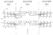
- eight signal lines 22 drawn to the leftare shown. Each signal line 22 was numbered 1-8 from the left side.
- signal line 2is floated and signal line 3 is grounded.
- signal lines 1 and 3are floated, and signal line 4 is grounded.
- the signal lines 2 and 4are floated in the section where the level shift is detected by the signal line 3, and the signal lines 1 and 5 are grounded.
- Each linecan be scanned as above, and five signal lines can be grouped together to proceed while shifting the above scanning at the same time. In this way, if the signal lines on both sides of the signal line of the detection section are floated and the side signal lines of the floated signal line are grounded with a dynamic shield, the coupling between the signal lines can be more completely blocked.
- physical touch resolutionmay be limited due to the wiring of the transparent signal line 22a. 20 may also remove some limitations of the touch resolution in the same manner as in the embodiments of FIGS. 17 to 19. In addition, the touch resolution may be increased by other methods.
- FIG. 23shows another method of increasing touch resolution in the embodiment of FIG. 16 or 20.
- a plurality of drive ICs 30may be mounted on the substrate 50.
- the drive ICs 30are mounted in the form of COG on the glass substrate 50 as shown.
- the drive IC 30includes a master drive IC 30a for transmitting a touch signal to the outside, and a slave drive IC 30b connected to the master driver IC 30a and the communication channel 94 on the substrate 50. do.
- the master drive IC 30ais connected to an FPC 96a for exchanging signals with the outside. Since the slave drive IC 30b communicates with the master drive IC 30a through the communication channel 94, a separate FPC does not need to be connected. However, as shown in the drawing, the FPC 96b for power transmission may be connected to the slave drive IC 30b.
- the master drive IC 30amay give priority to each other, give a scanning order, or have an independent memory space. Process the signals.
- FIG. 24is a diagram illustrating another embodiment of the touch screen panel.
- the sensor pattern 10is arranged in a dot matrix form, whereas the embodiment of FIG. 24 illustrates that the sensor pattern 10 is arranged in a linear manner.
- an x-axis linear sensor pattern 10a and a y-axis linear sensor pattern 10bcross each other in the active region 90 of the substrate 50.
- Each of the linear sensor patterns 10a and 10bhas an opposing area 41a for forming a touch capacitance Ct and a connecting portion 41b for connecting the opposing area 41a with the touch input tool. It is composed.
- the x-axis linear sensor pattern 10a and the y-axis linear sensor pattern 10bcross each other at the connection portion 41b to form an intersection portion 42.
- the intersection 42is configured to mutually insulate the linear sensor patterns 10a and 10b of different axes.
- the connecting portion 41b of the x-axis linear sensor pattern 10ais first formed, and an insulating layer is formed thereon, and then the connecting portion 41b of the y-axis linear sensor pattern 10b passes through the insulating layer. do.
- a great advantage of the embodiment of FIG. 24is that the number of signal lines 22 wired to the invisible region 92 of the substrate 50 can be greatly reduced. If the size of the sensor pattern 10 is reduced, the physical touch resolution may be increased as compared with the previous embodiments without increasing the number of signal lines 22 wired to the edge portion of the substrate 50.
- FIGS. 25 and 26are cross-sectional views illustrating an installation example of a touch screen panel
- FIGS. 27 and 28are cross-sectional views and an exploded perspective view of a display device incorporating a touch screen panel. Referring to this, a touch screen panel and a display device incorporating the touch screen panel according to the present invention will be described.
- the display device 200has a structure in which a liquid crystal is sealed between the lower TFT substrate 205 and the upper color filter 215 to form the liquid crystal layer 210.
- the TFT substrate 205 and the color filter 215are bonded by the sealant 230 at the outer portion thereof.
- polarizersare attached to the upper and lower sides of the liquid crystal panel, and optical sheets such as a BLU (Back Light Unit) and a Brightness Enhancement Film (BEF) are installed.
- BLUBack Light Unit
- BEFBrightness Enhancement Film
- a touch screen panelis installed on the display device 200 as shown.
- the touch screen panelhas a configuration in which the sensor pattern 10 and the common electrode 20 are provided on the upper and lower surfaces of the substrate 50 as in the embodiment of FIG. 7.
- a protection panel 52is attached to the top surface of the device to protect the touch screen panel.
- the touch screen panelis disposed on the upper portion of the display device 200 through an adhesive member 57 such as a DAT at an outer portion thereof.
- the air gap 58is formed between the touch screen panel and the display device 200. In such a structure, since Cp becomes very small, a more stable touch signal can be obtained.
- the LCD 25 and 26may be added over various types of display devices.
- the LCDitself has Vcom. If the Vcom electrode of the LCD is a transverse electric field mode formed on the TFT substrate 205, the noise caused by the Vcom of the LCD is relatively small. On the contrary, if the Vcom electrode 220 of the LCD is formed on the lower surface of the color filter 215 as shown in FIGS. 25 and 26, and the Vcom electrode 220 performs line inversion, noise caused by this may be relatively large.
- the distance to the sensor pattern 10is lower than that of the common electrode 20 on the lower surface of the substrate 50. It is considerable.
- the substrate 50acts as a medium between the sensor pattern 10 and the common electrode 20, the substrate 50 and the air gap 58 may be disposed between the sensor pattern 10 and the Vcom electrode 220 of the display device.
- a mediumsuch as an ultraviolet curable resin 98, a polarizing plate, a BEF, a color filter 215, or the like. Therefore, the influence of the Vcom electrode 220 of the LCD is minimal.
- the Cp due to the minor influencecan be sufficiently filtered out by the level shift detection unit 14.
- FIGS. 27 and 28illustrate a display device with a built-in touch screen panel according to the present invention, illustrating an LCD.
- the color filter 215 of the display device 200may be replaced with the touch screen panel according to the present invention.
- the sensor pattern 10is formed on the top surface of the color filter 215, and the common electrode 20 is formed on the bottom surface of the color filter 215.
- a protective panel 52may be additionally installed on the upper surface of the display device 200. The protection panel 52 prevents the display device 200 from being damaged by the touch input.
- the protection panel 52may serve as a window on which a company logo or icon is printed.
- the TFT IC 205is mounted with a drive IC 60 in the form of COG.
- the drive IC 30 for controlling the touch signalis mounted in the form of a COG.
- the FPCs 96 and 97are drawn out.
- the common electrode 20may be used as a common electrode of the display device.
- the alternating common voltage applied to the common electrode 20may be applied by the alternating voltage applying unit 37 of the touch drive IC 30, or may be applied by the LCD drive IC 60. Further, the touch drive IC 30 and the LCD drive IC 60 may be integrated into a single IC.
- the TFT substrate 205 and the color filter 215may be connected to the FPC to transmit and receive signals.
- the touch screen panelmay be installed between the color filter 215 and the polarizer not shown.
- the present inventionis not limited to the above-described embodiments and the accompanying drawings, and it is common in the art that various substitutions, modifications, and changes can be made without departing from the technical spirit of the present invention. It will be evident to those who have knowledge of.
- a common electrode having a planar shapeis spaced apart from the sensor pattern to form a common electrode.
Landscapes
- Engineering & Computer Science (AREA)
- General Engineering & Computer Science (AREA)
- Theoretical Computer Science (AREA)
- Human Computer Interaction (AREA)
- Physics & Mathematics (AREA)
- General Physics & Mathematics (AREA)
- Position Input By Displaying (AREA)
Abstract
Description
Translated fromKorean본 발명은 신체의 손가락 또는 이와 유사한 도전특성을 갖는 터치입력도구의 정전식 터치입력을 검출하는 방법 및 장치에 관한 것이다. 보다 상세하게는 공통전극과 센서패턴 사이에서 형성되는 공통전극정전용량에 터치입력에 의한 터치정전용량이 부가될 때, 전압의 레벨시프트 현상이 발생하는 것을 감지하여 터치신호를 획득하는 터치입력 검출 방법 및 장치에 관한 것이다.The present invention relates to a method and apparatus for detecting a capacitive touch input of a finger or a touch input tool having similar conductive characteristics. More specifically, the touch input detection method of detecting a level shift phenomenon of a voltage when the touch capacitance is added to the common electrode capacitance formed between the common electrode and the sensor pattern to obtain a touch signal. And to an apparatus.
일반적으로, 터치스크린패널(Touch Screen Panel)은 LCD(Liquid Crystal Display), PDP(Plasma Display Panel), OLED(Organic Light Emitting Diode), AMOLED(Active Matrix Organic Light Emitting Diode) 등의 표시장치 위에 부착되는 것으로서, 손가락이나 펜 등의 물체가 터치될 때 해당 위치에 대응하는 신호를 발생시키는 입력장치의 하나이다. 터치스크린패널은 소형 휴대단말기, 산업용 단말기, DID(Digital Information Device) 등 매우 폭넓은 분야에서 이용되고 있다.In general, a touch screen panel is attached to a display device such as a liquid crystal display (LCD), a plasma display panel (PDP), an organic light emitting diode (OLED), an active matrix organic light emitting diode (AMOLED), or the like. As an input device, a signal corresponding to a corresponding position is generated when an object such as a finger or a pen is touched. Touch screen panels are used in a wide range of applications, such as small portable terminals, industrial terminals, and digital information devices (DIDs).
종래 터치스크린패널은 다양한 유형이 개시되어 있으나, 제조공정이 간단하고 제조 코스트가 저렴한 저항 방식의 터치스크린패널이 가장 널리 이용되고 있다. 그러나 상기 저항 방식의 터치스크린패널은 투과율이 낮고 압력을 인가해야 하므로 사용이 불편하다. 또한, 상기 저항 방식의 터치 스크린 패널은 멀티 터치 및 제스처 인식이 어려운 문제점을 안고 있다.Conventional touch screen panels are disclosed in various types, but a resistive touch screen panel having a simple manufacturing process and a low manufacturing cost is most widely used. However, since the resistive touch screen panel has a low transmittance and a pressure must be applied, it is inconvenient to use. In addition, the resistive touch screen panel has a problem that it is difficult to recognize the multi-touch and gesture.
이에 반해, 정전식 터치스크린패널은 투과율이 높고 소프트 터치를 인식할 수 있고 멀티터치 및 제스처 인식이 양호한 장점을 갖고 있어 점차 시장을 넓혀가고 있다.In contrast, the capacitive touch screen panel has a high transmittance, a soft touch can be recognized, and multi-touch and gesture recognition have advantages of expanding the market.
도 1은 종래 정전식 터치스크린패널의 일예를 보여준다.1 shows an example of a conventional capacitive touch screen panel.
도 1을 참조하면, 플라스틱 또는 유리 등으로 제조된 투명기판(2)의 상하면에 투명도전막이 형성되며, 투명기판(2)의 네 모서리 각각에 전압인가용 금속전극(4)이 형성되어 있다. 상기 투명도전막은 ITO(Indium Tin Oxide) 또는 ATO(Antimony Tin Oxide) 등의 투명한 금속으로 형성된다. 그리고 상기 투명도전막의 네 모서리에 형성되는 금속전극(4)들은 은(Ag) 등의 저항률이 낮은 도전성 금속으로 프린팅하여 형성한다. 상기 금속전극(4)들의 주변에는 저항 네트워크가 형성된다. 상기 저항 네트워크는 상기 투명도전막의 표면 전체에 균등하게 컨트롤신호를 송출하기 위하여 선형성 패턴(Linearization Pattern)으로 형성된다. 그리고 금속전극(4)을 포함한 투명도전막의 상부에는 보호막이 코팅된다.Referring to FIG. 1, a transparent conductive film is formed on upper and lower surfaces of a
위와 같은 정전식 터치스크린패널은 상기 금속전극(4)에 고주파의 교류 전압을 인가하면 이는 투명기판(2)의 전면에 퍼지게 된다. 이때 손가락(8)이나 도전성 터치입력도구로 투명기판(2) 상면의 투명도전막을 가볍게 터치하면, 일정량의 전류가 체내로 흡수되면서 컨트롤러(6)에 내장된 전류센서에서 전류의 변화를 감지하고 4개의 금속전극(4) 각각에서의 전류량을 연산하여 터치 지점을 인식하게 된다.In the capacitive touch screen panel as described above, when an alternating current voltage of high frequency is applied to the
그런데, 도 1과 같은 정전식 터치스크린패널은 미소 전류의 크기를 검출하는 방식으로서, 고가의 검출장치를 필요로 하므로 가격이 상승하며 복수개의 터치를 인식하는 멀티터치가 어려운 문제점이 있다.However, the capacitive touch screen panel as shown in FIG. 1 is a method of detecting the magnitude of the micro current, and thus requires an expensive detection device, which increases the price and makes it difficult to multi-touch to recognize a plurality of touches.
이러한 문제점을 극복하기 위하여 근래에는 도 2와 같은 정전식 터치스크린패널이 주로 사용되고 있다. 도 2의 터치스크린패널은 횡방향의 선형센서패턴(5a) 및 종방향의 선형센서패턴(5b), 터치신호를 분석하는 터치드라이브IC(7)로 이루어져 있다. 이러한 터치스크린패널은 선형센서패턴(5)과 손가락(8) 사이에 형성되는 커패시턴스의 크기를 검출하는 방식으로서, 횡방향의 선형센서패턴(5a)과 종방향의 선형센서패턴(5b)을 스캔하여 신호를 검출하므로 복수개의 터치지점을 인식할 수 있다.In order to overcome this problem, the capacitive touch screen panel as shown in FIG. 2 is mainly used. The touch screen panel of FIG. 2 includes a
그런데, 위와 같은 터치스크린패널은 LCD와 같은 표시장치 위에 실장되어 사용될 때, 노이즈에 의해 신호 검출이 어려운 현상이 발생한다. 예컨대, LCD는 공통전극을 사용하며 경우에 따라 이 공통전극에 교류의 공통전압(Vcom)이 인가된다. 그리고 공통전극의 공통전압(Vcom)은 터치지점 검출시 노이즈로 작용한다.However, when the touch screen panel as described above is mounted and used on a display device such as an LCD, a phenomenon in which signal detection is difficult due to noise occurs. For example, the LCD uses a common electrode, and in some cases, an AC common voltage Vcom is applied to the common electrode. The common voltage Vcom of the common electrode acts as noise when detecting the touch point.
도 3은 LCD 위에 종래 정전식 터치스크린패널이 설치된 실시태양을 보여준다. 표시장치(200)는 하측의 TFT기판(205)과 상측의 칼라필터(215) 사이에 액정이 봉입되어 액정층(210)을 형성하는 구조를 갖는다. 액정의 봉입을 위하여 TFT기판(205)과 칼라필터(215)는 그 외곽부에서 실런트(230)에 의해 접합된다. 도시하지 않았지만, 액정패널의 상하로는 편광판이 부착되며, 그밖에도 BLU(Back Light Unit)와, BEF(Brightness Enhancement Film) 등과 같은 광학시트들이 설치된다.3 shows an embodiment in which a conventional capacitive touch screen panel is installed on an LCD. The
표시장치(200)의 상부에는 도시한 바와 같이 터치스크린패널이 설치된다. 터치스크린패널은 기판(1) 상면에 상기한 선형센서패턴(5)이 올려진 구조를 갖는다. 기판(1)의 위에는 선형센서패턴(5)을 보호하기 위한 보호패널(3)이 부착된다. 터치스크린패널은 DAT(Double Adhesive Tape) 등과 같은 접착부재(9)를 매개로 표시장치(200)의 에지부에 접착되며, 표시장치(200)와의 사이에서 에어갭(9a)을 형성한다.A touch screen panel is installed on the
이러한 구성에서 도 3에서와 같은 터치가 발생할 경우, 손가락(8)과 선형센서패턴(5) 사이에는 Ct와 같은 정전용량이 형성된다. 그런데, 도시한 바와 같이 선형센서패턴(5)과 표시장치(200)의 칼라필터(215) 하면에 형성된 공통전극(220) 사이에서도 Cvcom과 같은 정전용량이 형성되며, 선형센서패턴(5)에는 미지의 기생정전용량인 Cp도 작용하고 있다. 따라서, 도 4의 등가회로와 같은 회로가 구성된다.In this configuration, when a touch as shown in FIG. 3 occurs, a capacitance such as Ct is formed between the
여기서, 종래 터치스크린패널은 Ct의 변화량을 검출해서 터치를 인식하는데, Cvcom 및 Cp와 같은 백그라운드(Background) 성분은 Ct의 검출에 있어 노이즈로 작용한다. 예컨대 휴대기기용 중소형 LCD에서는 소비전류를 감소시키기 위하여 공통전극(220)의 공통전압(Vcom)이 도 5에서와 같이 하나 또는 복수의 게이트라인별로 교번하는 Line inversion 방식을 사용하므로, 이러한 교번 전계는 터치 검출시 상당한 노이즈로 작용한다.Here, the conventional touch screen panel detects a touch by detecting a change amount of Ct, and background components such as Cvcom and Cp act as noise in detecting Ct. For example, in the small and medium-sized LCD for portable devices, since the common voltage Vcom of the
통상적으로 위와 같은 노이즈를 제거하기 위하여, 도 3에서와 같이 터치스크린패널과 표시장치(200) 사이에 에어갭(9a)을 둔다. 또한, 도시하지 않았지만, 터치스크린패널의 기판(1) 하면에 ITO 등을 도포하여 차폐층을 형성하고 이 차폐층을 그라운드 신호와 접지시킨다.Typically, in order to remove the noise as described above, an
하지만, 종래 기술은 에어갭(9a)에 의해 제품의 두께가 증가하며 품질저하가 발생시킨다. 또한 종래 기술은 차폐층을 구성하기 위한 별도의 공정을 필요로 하므로 제조단가의 상승이 유발시킨다. 특히 LCD 내에 터치스크린패널을 내장하는 경우 에어갭(9a)이나 차폐층의 형성이 불가능하므로 LCD 등의 표시장치에 터치스크린패널을 내장하여 제조하는 것이 불가능하였다.However, in the prior art, the thickness of the product is increased by the
본 발명은 상기와 같은 종래 정전식 터치스크린패널의 문제점을 해결하기 위하여 제안된 것으로서, 외부의 노이즈에 의한 영향, 기생정전용량에 의한 영향 및 표시장치의 공통전극에 의한 영향을 최소화한다. 또한, 본 발명은 터치신호를 안정적으로 검출하는 동시에 LCD 등의 표시장치에 터치스크린패널을 내장하는 것이 용이한 새로운 방식의 터치 검출 장치 및 방법, 상기 터치 검출 장치을 내장한 표시장치를 제공한다.The present invention is proposed to solve the problems of the conventional capacitive touch screen panel as described above, and minimizes the influence of external noise, the parasitic capacitance, and the influence of the common electrode of the display device. In addition, the present invention provides a touch detection device and method of a novel method that is easy to detect a touch signal and at the same time easy to incorporate a touch screen panel in a display device such as LCD, and a display device incorporating the touch detection device.
본 발명의 한 측면에 따른 정전식 터치 검출 장치는, 터치입력도구와의 사이에서 터치정전용량(Ct)을 형성하며, 공통전극과 이격 배치되어 공통전극정전용량(Cvcom)을 형성하는 센서패턴; 상기 센서패턴에 충전신호를 공급하여 상기 공통전극정전용량(Cvcom)에 전하를 축적하기 위한 충전 수단; 및 상기 센서패턴에 연결되며, 터치 미발생시의 상기 센서패턴에서의 전압변동분에 대해, 터치 발생시의 상기 센서패턴에서의 전압변동분에 레벨시프트가 발생하는 것을 검출하여 터치신호를 획득하는 레벨시프트 검출부를 포함한다. 여기서, 상기 공통전극은 소정 주파수로 교번하는 공통전압(Vcom) 레벨을 가지며, 상기 레벨시프트 검출부는 터치 발생 전후에서 상기 공통전압(Vcom)에 의해 상기 센서패턴에서 발생하는 전압 변동분 사이의 레벨 시프트를 검출한다.According to an aspect of the present invention, there is provided a capacitive touch detection apparatus, comprising: a sensor pattern forming a touch capacitance Ct between a touch input tool and spaced apart from a common electrode to form a common electrode capacitance Cvcom; Charging means for supplying a charging signal to the sensor pattern to accumulate charge in the common electrode capacitance (Cvcom); And a level shift detection unit connected to the sensor pattern and detecting a level shift occurring in the voltage variation in the sensor pattern at the time of touch generation with respect to the voltage variation in the sensor pattern when the touch is not generated. Include. Here, the common electrode has a common voltage Vcom level alternated at a predetermined frequency, and the level shift detection unit performs a level shift between voltage variations generated in the sensor pattern by the common voltage Vcom before and after a touch occurs. Detect.
상기 터치 미발생시 전압변동은 다음의 <수식1>에 의해 결정되고, 상기 터치정전용량(Ct)이 부가될 때 전압변동은 다음의 <수식2>에 의해 결정되며, 상기 레벨시프트는 <수식1>과 <수식2>의 전압 변동분의 차이이다.When the touch is not generated, the voltage variation is determined by
<수식1>
<수식2>
여기서,


상기 레벨시프트 검출부는 상기 공통전압 레벨의 상승구간(rising time) 및/또는 하강구간(falling time)에서 센서패턴에서의 레벨시프트를 검출한다.The level shift detection unit detects a level shift in the sensor pattern at a rising time and / or a falling time of the common voltage level.
상기 레벨시프트 검출부는 레벨시프트의 크기에 기초하여 상기 센서패턴에 대한 터치입력도구의 터치 점유율을 검출할 수 있다.The level shift detector may detect a touch occupancy rate of the touch input tool with respect to the sensor pattern based on the magnitude of the level shift.
상기 레벨시프트 검출부는 상기 센서패턴에서의 신호를 차동 증폭하는 차동증폭기를 포함할 수 있다.The level shift detector may include a differential amplifier for differentially amplifying a signal in the sensor pattern.
또한, 상기 터치 검출 방법은 상기 공통전극에 상기 공통전압을 인가하는 공통전압 인가부를 더 포함할 수 있다.The touch detection method may further include a common voltage applying unit configured to apply the common voltage to the common electrode.
본 발명의 다른 측면에 따른, 터치 검출 방법은 상기 센서패턴과 상기 센서 패턴에 형성된 공통전극정전용량(Cvcom)에 충전신호를 공급하는 단계; 상기 충전 신호의 공급을 중단하고 상기 충전 신호의 전하를 고립시키는 단계; 상기 공통전극정전용량(Cvcom)에 인가되는 공통전압(Vcom)에 의해 상기 센서패턴에서의 전압변동분을 검출하는 단계; 및 터치 발생 전후의 상기 전압변동분사이의 레벨시프트가 발생하는 것을 검출하여 터치 신호를 획득하는 단계를 포함한다.According to another aspect of the invention, the touch detection method comprises the steps of: supplying a charging signal to the sensor pattern and the common electrode capacitance (Cvcom) formed in the sensor pattern; Stopping the supply of the charge signal and isolating charge of the charge signal; Detecting a voltage variation in the sensor pattern by a common voltage Vcom applied to the common electrode capacitance Cvcom; And detecting a level shift between the voltage fluctuations before and after the touch occurs to obtain a touch signal.
상기 터치 검출 방법은, 상기 센서패턴에서의 신호를 차동 증폭하는 단계를 더 포함할 수 있다.The touch detection method may further include differentially amplifying a signal in the sensor pattern.
상기 차동 증폭 단계에서, 차동 입력 신호는 터치 미발생시의 상기 전압 변동분일 수 있다. 이 때, 상기 터치 검출 방법은 각각의 센서패턴에 대하여 상기 터치 미발생시의 전압변동분을 메모리에 저장하는 단계를 더 포함할 수 있다.In the differential amplifying step, the differential input signal may be the voltage change when no touch occurs. In this case, the touch detection method may further include storing the voltage variation when the touch is not generated in the memory for each sensor pattern.
본 발명의 또 다른 측면에 따른 정전식 터치 장치를 내장한 표시 장치는, 터치입력도구와의 사이에서 터치정전용량(Ct)을 형성하며, 공통전극과 이격 배치되어 공통전극정전용량(Cvcom)을 형성하는 센서패턴; 상기 센서패턴에 충전신호를 공급하여 상기 공통전극정전용량(Cvcom)에 전하를 축적하기 위한 충전 수단; 및 상기 센서패턴에 연결되며, 터치 미발생시의 상기 센서패턴에서의 전압변동분에 대해, 터치 발생시의 상기 센서패턴에서의 전압변동분에 레벨시프트가 발생하는 것을 검출하여 터치신호를 획득하는 레벨시프트 검출부를 포함한다. 여기서, 상기 공통전극은 소정 주파수로 교번하는 공통전압(Vcom) 레벨을 가지며, 상기 레벨시프트 검출부는 터치 발생 전후에서 상기 공통전압(Vcom)에 의해 상기 센서패턴에서 발생하는 전압 변동분 사이의 레벨 시프트를 검출할 수 있다.According to another aspect of the present invention, a display device having a capacitive touch device includes a touch capacitance (Ct) between the touch input tool, and is spaced apart from the common electrode to form the common electrode capacitance (Cvcom). Forming a sensor pattern; Charging means for supplying a charging signal to the sensor pattern to accumulate charge in the common electrode capacitance (Cvcom); And a level shift detection unit connected to the sensor pattern and detecting a level shift occurring in the voltage variation in the sensor pattern at the time of touch generation with respect to the voltage variation in the sensor pattern when the touch is not generated. Include. Here, the common electrode has a common voltage Vcom level alternated at a predetermined frequency, and the level shift detection unit performs a level shift between voltage variations generated in the sensor pattern by the common voltage Vcom before and after a touch occurs. Can be detected.
상기 표시 장치의 정전식 터치 장치는 상기 공통전극의 공통전압 정보를 수신하는 공통 전압 수신부를 더 포함할 수 있다.The capacitive touch device of the display device may further include a common voltage receiver configured to receive common voltage information of the common electrode.
또한, 상기 표시 장치의 정전식 터치 장치는 상기 공통전극의 공통전압 레벨을 검출하는 공통 전압 검출부를 더 포함할 수 있다.The capacitive touch device of the display device may further include a common voltage detector configured to detect a common voltage level of the common electrode.
여기서, 상기 충전 수단 및 레벨시프트 검출부는 표시 장치의 비가시 영역에 설치될 수 있다.The charging means and the level shift detector may be installed in the invisible region of the display device.
본 발명의 레벨시프트를 이용한 정전식 터치 검출 장치, 검출방법 및 터치스크린패널과, 그러한 정전식 터치스크린패널을 내장한 표시장치에 따르면, 표시장치로부터의 수직적인 노이즈, 커플링 현상이나 기타 요인에 의해 생성되는 기생정전용량 등에 의한 영향이 최소화되고 신호의 오인식이 발생하지 않게 된다.According to the capacitive touch detection device, the detection method and the touch screen panel using the level shift of the present invention, and the display device incorporating such a capacitive touch screen panel, it is possible to reduce the vertical noise, coupling phenomenon and other factors from the display device. By the parasitic capacitance generated by the effect is minimized and the signal misrecognition is not generated.
또한, 터치입력을 비교적 높은 전압레벨로 검출함으로써 터치입력도구의 단면이 작아도 신호의 포착이 용이하고 스타일러스 펜 입력이 가능하다.In addition, by detecting the touch input at a relatively high voltage level, even if the cross section of the touch input tool is small, the signal is easily captured and the stylus pen input is possible.
또한, 레벨시프트의 크기에 따라 터치입력도구의 터치 점유율을 구함으로써 터치 해상도를 높이고 미세한 필기 및 드로잉이 가능하도록 한다.In addition, by obtaining the touch occupancy ratio of the touch input tool according to the size of the level shift, the touch resolution is increased and fine writing and drawing are possible.
또한, 터치 패널의 액티브영역을 단일 레이어로 구성할 수 있어 제조공정이 간소화되고 수율이 양호한 효과가 있다.In addition, since the active area of the touch panel can be configured as a single layer, the manufacturing process is simplified and the yield is good.
도 1은 종래 정전식 터치스크린패널의 일예를 보인 사시도1 is a perspective view showing an example of a conventional capacitive touch screen panel
도 2는 종래 정전식 터치스크린패널의 다른 예를 보인 평면구성도2 is a plan view showing another example of a conventional capacitive touch screen panel
도 3은 도 2의 터치스크린패널이 표시장치 위에 설치된 예를 보인 단면도3 is a cross-sectional view illustrating an example in which the touch screen panel of FIG. 2 is installed on a display device.
도 4는 도 3에서 터치정전용량을 검출하는 등가 회로도4 is an equivalent circuit diagram of detecting a touch capacitance in FIG. 3.
도 5는 액정표시장치의 공통전압 파형을 예시한 파형도5 is a waveform diagram illustrating a common voltage waveform of a liquid crystal display device;
도 6은 본 발명에 따른 터치 검출 장치를 예시한 회로도6 is a circuit diagram illustrating a touch detection device according to the present invention.
도 7a는 본 발명의 일 실시예에 따른 터치스크린패널의 단면도7A is a cross-sectional view of a touch screen panel according to an embodiment of the present invention.
도 7b는 본 발명의 일 실시예에 따른 터치스크린패널과 표시 장치의 단면도7B is a cross-sectional view of a touch screen panel and a display device according to an embodiment of the present invention.
도 8은 터치 검출 장치의 일예를 보인 회로도8 is a circuit diagram illustrating an example of a touch detection apparatus;
도 9는 도 8의 실시예에서 터치신호를 검출하는 과정을 보인 파형도9 is a waveform diagram illustrating a process of detecting a touch signal in the embodiment of FIG. 8;
도 10은 TFT의 게이트전압 대비 출력전류의 특성을 보인 그래프10 is a graph showing the characteristics of the output current compared to the gate voltage of the TFT
도 11a 및 11b는 터치 검출 장치의 다른 예를 보인 회로도11A and 11B are circuit diagrams illustrating another example of the touch detection apparatus.
도 12는 도 11의 실시예에서 터치신호를 검출하는 과정을 보인 파형도12 is a waveform diagram illustrating a process of detecting a touch signal in the embodiment of FIG. 11;
도 13은 메모리부의 구성예를 보인 블록도13 is a block diagram showing an example of the configuration of a memory unit;
도 14a는 터치스크린패널의 일실시예를 보인 구성도14A is a block diagram showing an embodiment of a touch screen panel
도 14b는 터치스크린패널의 일실시예를 보인 구성도14B is a block diagram showing an embodiment of a touch screen panel
도 15a 내지 15d는 신호처리부의 실시예를 보인 회로도15A to 15D are circuit diagrams showing an embodiment of a signal processing unit;
도 16은 터치스크린패널의 다른 실시예를 보인 구성도16 is a configuration diagram showing another embodiment of the touch screen panel
도 17 내지 19는 센서패턴을 복수의 레이어로 구성하는 예를 순차적으로 보인 구성도17 to 19 are configuration diagrams sequentially showing an example of configuring the sensor pattern in a plurality of layers
도 20은 터치스크린패널의 또 다른 실시예를 보인 구성도20 is a configuration diagram showing another embodiment of the touch screen panel
도 21은 도 20의 실시예에서 커플링을 최소화하는 예를 보인 구성도21 is a diagram illustrating an example of minimizing coupling in the embodiment of FIG. 20.
도 22는 도 20의 실시예에서 커플링을 최소화하는 다른 예를 보인 구성도22 is a diagram illustrating another example of minimizing coupling in the embodiment of FIG. 20.
도 23은 복수의 드라이브IC가 설치된 예를 보인 평면도23 is a plan view showing an example in which a plurality of drive ICs are installed
도 24는 터치스크린패널의 또 다른 실시예를 보인 구성도24 is a configuration diagram showing another embodiment of the touch screen panel
도 25는 터치스크린패널의 설치예를 보인 단면도25 is a cross-sectional view showing an example of installation of the touch screen panel.
도 26은 터치스크린패널의 다른 설치예를 보인 단면도26 is a cross-sectional view showing another example of installation of the touch screen panel.
도 27은 본 발명에 따른 터치스크린패널을 내장한 표시장치의 단면도27 is a cross-sectional view of a display device having a touch screen panel according to the present invention.
도 28은 도 26의 실시예를 분해 도시한 사시도28 is an exploded perspective view illustrating the embodiment of FIG. 26.
이하, 본 발명의 바람직한 실시예를 첨부된 도면 및 실시예를 참조하여 상세히 설명한다.Hereinafter, preferred embodiments of the present invention will be described in detail with reference to the accompanying drawings and embodiments.
우선, 본 발명은 레벨시프트를 이용한 정전식 터치 검출 장치, 검출방법 및 터치스크린패널과, 그러한 정전식 터치스크린패널을 내장한 표시장치에 관한 것으로서, 종래의 정전식 터치 검출수단이 손가락 등의 접촉에 의한 커패시턴스의 변화를 검출하는 방식인 것과 달리, 교번 전압을 갖는 공통전극을 구성하고 이 공통전극과 센서패턴의 상호관계에 의해 발생하는 전압변동을 검출하는 방식이다.Firstly, the present invention relates to a capacitive touch detection device using a level shift, a detection method and a touch screen panel, and a display device incorporating such a capacitive touch screen panel. Unlike a method of detecting a change in capacitance due to the above-described method, a common electrode having an alternating voltage is formed, and a voltage change generated by the mutual relationship between the common electrode and the sensor pattern is detected.
본 발명에 따른 터치 검출 시스템은 터치 미발생시 공통전극과 센서패턴 상호간의 공통전극정전용량에 의한 전압변동분과, 터치 발생에 의해 공통전극정전용량에 터치정전용량이 부가될 때의 전압변동분을 비교하고, 두 전압변동분 상호간의 크기 차이인 레벨시프트를 검출함으로써, 표시장치에서 발생되는 노이즈나 기생정전용량 등에 의한 영향이 최소화 되며, 보다 안정적으로 터치신호를 획득할 수 있다.The touch detection system according to the present invention compares the voltage variation due to the common electrode capacitance between the common electrode and the sensor pattern when no touch occurs, and the voltage variation when the touch capacitance is added to the common electrode capacitance due to touch generation. By detecting a level shift, which is a magnitude difference between two voltage variations, the influence of noise or parasitic capacitance generated in the display device is minimized, and a touch signal can be obtained more stably.
본 발명은 손가락이나 이와 유사한 전기적 특성을 갖는 터치입력도구의 비접촉 터치입력을 검출한다. 여기서 "비접촉 터치입력"이라 함은 손가락 등의 터치입력도구가 기판에 의해 센서패턴과 소정 거리 이격된 상태에서 터치입력을 하는 것을 의미한다. 터치입력도구가 기판의 외면에 대하여는 접촉될 수 있다. 하지만 이 경우에도 터치입력도구와 센서패턴은 비접촉 상태를 유지한다. 따라서, 센서패턴에 대한 손가락의 터치 행위는 "접근"이라는 용어로 표현될 수 있다. 한편, 기판의 외면에 대하여는 손가락이 접촉된 상태일 수 있으므로, 기판에 대한 손가락의 터치 행위는 "접촉"이라는 용어로 표현될 수 있다. 본 명세서에서 "접근"과 "접촉"은 위와 같은 의미로 통용된다.The present invention detects a non-contact touch input of a touch input tool having a finger or similar electrical characteristics. Here, the term "non-contact touch input" means that a touch input tool such as a finger makes a touch input while being spaced apart from the sensor pattern by a substrate at a predetermined distance. The touch input tool may contact the outer surface of the substrate. However, even in this case, the touch input tool and the sensor pattern remain in a non-contact state. Therefore, the touch action of the finger on the sensor pattern may be expressed by the term "access". On the other hand, since the finger may be in contact with the outer surface of the substrate, the touch action of the finger against the substrate may be expressed by the term "contact". In this specification, "access" and "contact" are commonly used as the meaning above.
또한, 이하에서 설명되는 "~부"와 같은 구성들은 어떤 역할들을 수행하는 구성요소이며, 소프트웨어 또는 FPGA(Field-Programmable Gate Array)나 ASIC(Application Specific Integrated Circuit)와 같은 하드웨어 구성요소를 의미한다. 그렇지만, "~부"는 소프트웨어 또는 하드웨어에 한정되는 의미는 아니다. 예컨대, "~부"는 어드레싱할 수 있는 저장매체에 구성될 수도 있고, 하나 또는 그 이상의 프로세서들을 재생시키도록 구성될 수도 있다. 일예로서, "~부"는 어떤 프로세스들, 함수들, 속성들, 서브루틴들, 프로그램 코드의 세그먼트들, 펌웨어, 마이크로코드, 데이터베이스, 변수들을 포함할 수 있다. 또한, "~부"는 더 큰 구성요소 또는 "~부"에 포함되거나, 더 작은 구성요소들 및 "~부"들을 포함할 수 있다. 또한, "~부"는 자체적으로 독자적인 CPU를 가질 수도 있다.In addition, components described below are components that perform certain roles, and refer to software or hardware components such as a field-programmable gate array (FPGA) or an application specific integrated circuit (ASIC). However, "~ part" is not meant to be limited to software or hardware. For example, " ~ " may be configured in an addressable storage medium or may be configured to play one or more processors. As an example, "~ part" may include certain processes, functions, properties, subroutines, segments of program code, firmware, microcode, database, variables. Also, "~ part" may be included in larger component or "~ part" or may include smaller components and "~ part". Also, the "~ part" may have its own CPU.
이하의 도면에서 여러 층 및 영역을 명확하게 표현하기 위하여 두께나 영역을 확대하여 나타내었다. 명세서 전체를 통하여 유사한 부분에 대해서는 동일한 도면부호를 사용하였다. 층, 막, 영역, 기판 등의 부분이 다른 부분 "위에" 또는 "상면" 있다고 할 때, 이는 다른 부분 "바로 위에" 있는 경우 뿐 아니라 그 중간에 또 다른 부분이 있는 경우도 포함한다. 반대로 어떤 부분이 다른 부분 "바로 위에" 있다고 할 때에는 중간에 다른 부분이 없는 것을 뜻한다. 또한, 본 명세서에 기재된 신호는 특별한 언급이 없는 한, 전압 또는 전류를 총칭한다.In the drawings, thicknesses or regions are enlarged in order to clearly express various layers and regions. The same reference numerals are used for similar parts throughout the specification. When a portion of a layer, film, region, substrate, etc. is said to be "on top" or "top" of another part, this includes not only the case where the other part is "right over" but also another part in the middle. On the contrary, when a part is "just above" another part, there is no other part in the middle. In addition, the signals described herein collectively refer to voltage or current, unless otherwise noted.
도 6은 본 발명에 따른 터치 검출 장치를 예시한 회로도이다.6 is a circuit diagram illustrating a touch detection device according to the present invention.
도 7a은 본 발명의 실시예에 따라 공통전극이 형성된 터치스크린패널의 기본적인 구성을 보인 단면도이다.7A is a cross-sectional view illustrating a basic configuration of a touch screen panel in which a common electrode is formed according to an exemplary embodiment of the present invention.
도 7b는 본 발명의 실시예에 다라 표시장치에 공통전극이 형성된 터치스크린패널과 표시장치의 구성을 보인 단면도이다.7B is a cross-sectional view illustrating a configuration of a touch screen panel and a display device in which a common electrode is formed in the display device according to an exemplary embodiment of the present invention.
우선 도 6을 참조하면, 본 발명의 터치 검출 장치는 기본적으로 센서패턴(10)과, 공통전극(20)과, 충전 수단(12)과, 레벨시프트 검출부(14)로 구성된다.First, referring to FIG. 6, the touch detection apparatus of the present invention basically includes a
센서패턴(10)은 터치입력 검출을 위해 패터닝 된 전극으로서, 신체의 손가락(25) 또는 이와 유사한 도전체와 같은 터치입력도구와의 사이에서 터치정전용량(Ct)을 형성한다. 센서패턴(10)은 표시장치의 위에 터치스크린패널이 올려지는 경우에 투명도전체로 형성된다. 예컨대, 센서패턴(10)은 ITO(Indium Tin Oxide), ATO(Antimony Tin Oxide), CNT(Carbon Nano Tube), IZO(Indium Zinc Oxide) 등의 투명 물질 또는 이와 유사한 도전특성을 갖는 투명 물질로 형성된다. 만약, 표시장치의 위가 아닌 터치 키보드, 터치패드 등의 터치스크린패널에서는 센서패턴(10)은 메탈(metal) 등으로 형성될 수도 있다.The
센서패턴(10)은 다양한 형태로 패터닝 될 수 있다. 예컨대, 기판(50)의 액티브영역에서 고립된 섬(island)들이 매트릭스 형태로 배열되는 도트 매트릭스 형태이거나, 선형의 패턴들이 기판(50)을 종횡하도록 배열될 수 있다. 센서패턴(10)의 형태에 대하여는 후술되는 실시예에서 설명하기로 한다.The
공통전극은 센서패턴(10)과 이격 형성되는 전극이다. 도 7a와 같이 공통전극(20)은 터치스크린패널에 형성될 수 있으며, 도 7b와 같이 공통전극(220)표시장치의 공통전극이 이용될 수 있다.The common electrode is an electrode spaced apart from the
도 7a에 도시된 실시예에서는 공통전극(20)이 센서패턴(10)과 균일한 간격을 유지하도록 하기 위해서, 도 7에서와 같이 기판(50)의 상면에는 센서패턴(10)이 형성되고 기판(50)의 하면에는 공통전극(20)이 형성될 수 있다. 공통전극(20)은 기판(50)의 하면 전체영역에 걸쳐 형성될 수 있다.In the embodiment shown in FIG. 7A, in order to maintain the
한편, 도 7a에 도시된 실시예에서 공통전극(20)은 후술할 레벨시프트를 검출하기 위하여 이용되는 것이기 때문에, 반드시 터치패널스크린 상에 물리적으로 형성되지 않고 도 6에 도시된 회로와 등가를 이루는 임의의 위치에 형성될 수 있다. 예를 들어, 각각의 도트 매트릭스형 센서패턴(10)과 Cvcom을 형성할 수 있도록 구동 드라이브 IC에 공통전극(20)이 형성될 수 있다.On the other hand, since the
공통전극(20)에는 소정 주파수로 교번하는 공통전압 레벨이 인가된다. 손가락(25)과 같은 도전체가 센서패턴(10)에 접근할 때 센서패턴(10)과 공통전극(20) 사이에는 공통전극정전용량(Cvcom)이 형성되며, 충전된 전압에 의해 공통전극정전용량(Cvcom)은 소정의 전압 레벨을 갖게 된다. 이때, 공통전극정전용량(Cvcom)의 일단은 공통전극(20)과 접지되어 있으므로, 공통전극(20)에 인가되는 교번 전계에 의해 공통전극정전용량(Cvcom)의 타단인 센서패턴(10)에서의 전위는 변동할 것이다. 즉, 센서패턴(10)의 전위는 공통전극정전용량(Cvcom)에 의해 전압변동 한다.The
한편, 상술한 Ct 및 Cvcom 등은 커패시터의 이름 및 크기를 동시에 표현하는 기호로서, 예컨대 "Ct"는 Ct라는 이름을 가진 커패시터를 의미하는 동시에 Ct라는 크기의 커패시턴스를 의미한다.Meanwhile, the above-mentioned Ct and Cvcom and the like are symbols representing the name and size of the capacitor at the same time. For example, "Ct" means a capacitor having the name Ct and a capacitance of the size Ct.
도 7b에 도시된 실시예에 따르면, 표시장치(200)가 공통전극(220)을 갖는다. 표시장치(200)는 앞서 언급한 다양한 형태의 표시장치일 수 있으며, 공통전극(220)은 LCD의 Vcom 전극이거나, 기타 다른 유형의 전극일 수 있다. 도 7의 실시예는 표시장치들 중 LCD를 예시하였다.According to the exemplary embodiment illustrated in FIG. 7B, the
도 7b에 도시된 표시장치(200)는 하측의 TFT기판(205)과 상측의 칼라필터(215) 사이에 액정이 봉입되어 액정층(210)을 형성하는 구조를 갖는다. 액정의 봉입을 위하여 TFT기판(205)과 칼라필터(215)는 그 외곽부에서 실런트(230)에 의해 접합된다. 도시하지 않았지만, 액정패널의 상하로는 편광판이 부착되며, 그밖에도 BLU(Back Light Unit)와, BEF(Brightness Enhancement Film) 등과 같은 광학시트들이 설치된다.The
표시장치(200)의 상부에는 도시한 바와 같이 터치스크린패널의 기판(50)이 설치된다. 도 7의 예시에서 기판(50)은 그 외곽부에서 DAT(Double Adhesive Tape) 등과 같은 접착부재(57)를 매개로 표시장치(200)의 상부에 부착된다. 그리고 기판(50)과 표시장치(200) 사이에는 에어갭(58)이 형성된다.As illustrated, a
표시장치(200)의 공통전극(220)에는 도 7b에서와 같이 소정 주파수로 교번하는 공통전압 레벨이 인가된다. 예컨대, 중소형 LCD는 공통전극(220)의 공통전압이 도 5에서와 같이 교번한다. 다른 예로서, 공통전극(220)의 공통전압이 일정하게 유지되거나, 공통전극(220)이 그라운드 신호와 접지되는 경우에는 공통전극(220)에 별도의 교번전압을 인가한다. 공통전극(220)에 교번전압을 인가하는 예에 대하여는 후술되는 실시예에서 상세히 설명하기로 한다.As shown in FIG. 7B, a common voltage level alternated at a predetermined frequency is applied to the
도 7a 및 7b를 참조하여 설명하였지만, 공통전극이 물리적으로 어디에 위치하였든 도 6과 등가 회로가 채택된다면 본 발명의 실시예에 따라 레벨 시프트를 검출할 수 있다.Although described with reference to FIGS. 7A and 7B, even if the common electrode is physically located, if the equivalent circuit of FIG. 6 is adopted, the level shift can be detected according to the embodiment of the present invention.
다시 도 6으로 돌아와 설명하며, 충전 수단(12)은 센서패턴(10)에 충전신호를 필요한 시점에 선택적으로 공급하는 수단이다. 충전 수단(12)은 온/오프 제어단자에 공급되는 제어신호에 따라 스위칭동작을 수행하는 3단자형의 스위칭소자이거나, 제어신호에 따라 신호를 공급하는 OP-AMP 등의 선형소자이다. 예컨대, 충전 수단(12)는 릴레이(Relay), MOS(Metal Oxide Semiconductor) 스위치, BJT(Bipolar Junction Transistor), FET(Field Effect Transistor), MOSFET(Metal Oxide Semiconductor Field Effect Transistor), IGBT(Insulated Gate Bipolar Transistor), TFT(Thin Film Transistor) 중 어느 하나이다. 릴레이는 제어단자에 전류를 인가하면 입력단자에 인가된 전압이나 전류가 손실 없이 출력되는 소자이며, BJT는 베이스(Base)의 문턱전압(Threshold Voltage)보다 높은 전압을 베이스에 인가한 상태에서 베이스단자에 전류를 흘리면 일정량 증폭된 전류가 콜렉터(Collector)에서 에미터(Emitter)로 흐르는 소자이다. 또한 TFT는 LCD나 AMOLED 등의 화소부에 사용되는 스위칭소자로서, 제어단자인 게이트(Gate)단자, 입출력단자인 드레인(Drain)단자 및 소스(Source)단자로 구성되며, 게이트단자로 소스단자에 인가된 전압보다 문턱전압 이상 되는 전압을 가하면, 도통되면서 게이트단자에 인가된 전압의 크기에 종속되는 전류가 입력단자에서 출력단자로 흐르는 소자이다. 또는, 충전 수단(12)으로는 Enable과 Disable 단자를 가진 OP-AMP나 플립플롭(Flip-Flop) 등 다양한 소자들이 사용될 수 있다.6 again, the charging means 12 is a means for selectively supplying a charging signal to the
도 6의 회로도를 참조하면, 충전 수단(12)의 출력단자에는 센서패턴(10)에 작용하는 Ct와 Cvcom이 연결된다. 따라서 충전 수단(12)을 턴 온 시킨 상태에서 입력단자에 임의의 전압이나 전류 등의 충전신호를 인가하면 Ct와 Cvcom이 충전된다. 이때, 도시하지 않은 기생정전용량(Cp;Parastic Capacitance) 역시 충전될 것이다.Referring to the circuit diagram of FIG. 6, Ct and Cvcom acting on the
이후 만약 충전 수단(12)을 턴 오프 시키면, Ct 및 Cvcom 등에 충전된 신호를 별도로 방전시키지 않는 한 충전된 신호는 고립된다. 충전된 신호를 안정적으로 고립시키기 위해서, 도 6에서와 같이 레벨시프트 검출부(14)의 입력단은 하이 임피던스(Hi-impedance 또는 Hi-z)를 갖는다. 만약 Ct 및 Cvcom에 충전된 신호를 방전시키면서 터치입력을 관찰하거나, 다른 수단으로 충전 신호를 고립시키거나, 방전 개시 시점에서 신속하게 신호를 관찰한다면, 레벨시프트 검출부(14)의 입력단이 반드시 Hi-z이어야 하는 것은 아니다.Thereafter, if the charging means 12 is turned off, the charged signal is isolated unless the charged signal is separately discharged to Ct and Cvcom. In order to stably isolate the charged signal, as shown in FIG. 6, the input terminal of the
레벨시프트 검출부(14)는 센서패턴(10)에서의 신호 레벨이 시프트 되는지 여부를 검출한다. 바람직하게는, 레벨시프트 검출부(14)는 터치 미발생시(즉, Ct가 형성되지 않을 때의) 센서패턴(10)에서의 전압변동에 대비하여, 터치 발생시(즉, Cvcom에 Ct가 병렬로 부가될 때의) 센서패턴(10)에서의 전압변동에 레벨시프트가 발생하는지를 검출하여 터치신호를 획득한다. 레벨시프트 검출부(14)는 다양한 소자 또는 회로구성을 가질 수 있다. 후술되는 실시예에서는 레벨시프트 검출부(14)로서 스위칭소자 및 차동증폭기가 사용되는 예를 설명하겠으나, 레벨시프트 검출부(14)의 구성은 그러한 실시예에 국한되지 않는다.The level
도 7a 및 도 7b를 참조하면, 손가락(25)과 센서패턴(10) 사이에는 터치정전용량(Ct)이 형성되며, 센서패턴(10)과 공통전극(20,220) 사이에는 공통전극정전용량(Cvcom)이 형성된다. 도 7a 및 7b에서 은선으로 표시된 것은 센서패턴(10)을 보호하기 위한 평탄층(24)이며, 만약 기판(50)의 상면에 강화 글래스 등과 같은 보호패널이 부착되면 위와 같은 평탄층(24)은 제거될 수 있다7A and 7B, a touch capacitance Ct is formed between the
터치 미발생시 Cvcom에 의한 센서패턴(10)에서의 전압변동은 다음의 <수식1>에 의해 결정된다.When no touch occurs, the voltage variation in the
<수식1>
터치 발생시 Cvcom에 Ct가 병렬로 부가되므로, 센서패턴(10)에서의 전압변동은 다음의 <수식2>에 의해 결정된다.Since Ct is added to Cvcom in parallel when a touch occurs, the voltage variation in the
<수식2>
위 <수식1> 및 <수식2>에서,


레벨시프트 검출부(14)는 위와 같은 <수식1>과 <수식2>를 이용하여 센서패턴(10)에서의 레벨시프트를 검출하며, 이에 대하여 상세히 설명하면 다음과 같다.The level
위 수식들에서 VcomH 및 VcomL는 쉽게 설정할 수 있는 값이다. 그리고 Cvcom은 다음의 <수식3>으로부터 얻을 수 있다.In the above formulas, VcomH and VcomL are easily set values. And Cvcom can be obtained from
<수식3>
<수식3>에서 은 기판(50)의 유전율로부터 얻을 수 있다. 예컨대, 글래스의 경우 비유전율이 3~5이므로, 여기에 진공의 유전율을 곱한 값으로부터 기판(50)의 유전율을 얻을 수 있다. S1은 센서패턴(10)과 공통전극(20)의 대향면적이므로 쉽게 구할 수 있다. 도 7a 및 7b의 예에서와 같이 기판(50)의 하면 전체에 걸쳐 공통전극이 형성된 경우, 대향면적 S1은 센서패턴(10)의 면적에 의해 결정된다. 또한, D1은 센서패턴(10)과 공통전극(20)간 거리이므로, 기판(50)의 두께에 해당된다.In
살펴 본 바와 같이 Cvcom은 쉽게 구할 수 있는 값인 동시에, 설정할 수 있는 값이다.As you can see, Cvcom is a value that can be easily obtained and set.
Ct는 다음의 <수식4>로부터 얻을 수 있다.Ct can be obtained from
<수식4>
<수식4>에서 ε은 센서패턴(10)과 손가락(25) 사이의 매질로부터 얻을 수 있다. 만약, 도 7에서 기판(50)의 상면에 강화 글래스를 부착한다면, 강화 글래스의 비유전율에 진공의 유전율을 곱한 값으로부터 유전율 ε을 얻을 수 있다. S2는 센서패턴(10)과 손가락(25)의 대향면적에 해당한다. 만약 손가락(25)이 어떤 센서패턴(10)을 모두 덮고 있다면 S2는 센서패턴(10)의 면적에 해당한다. 만약 손가락(25)이 센서패턴(10)의 일부를 덮고 있다면 S2는 손가락(25)과 대향하지 않은 면적만큼 줄어들 것이다. 또한, D2는 센서패턴(10)과 손가락(25)간 거리이므로, 기판(50) 상면에 올려진 강화 글래스 또는 평탄층(24) 등의 두께에 해당할 것이다.In
살펴 본 바와 같이 Ct 역시 쉽게 구할 수 있는 값인 동시에, 기판(50) 상부에 올려지는 보호패널 또는 평탄층(24) 등을 이용하여 쉽게 설정할 수 있는 값이다. 특히, <수식4>에 의하면 Ct는 손가락(25)과 센서패턴(10)의 대향면적에 비례하므로, 이로부터 센서패턴(10)에 대한 손가락(25)의 터치 점유율을 연산할 수 있다.As described above, Ct is also a value that can be easily obtained, and can be easily set using a protection panel or a
레벨시프트 검출부(14)는 위와 같은 <수식1>에 의한 전압변동에 대비하여 <수식2>에 의한 전압변동에 레벨시프트가 발생했는지 여부를 검출한다. 레벨시프트 검출부(14)는 센서패턴(10)에서의 신호를 증폭하는 증폭기, ADC(Analogue to Digital Converter), VFC(Voltage to Frequency Converter), 플립플롭(Flip-Flop), 래치(Latch), 버퍼(Buffer), TR(Transistor), TFT(Thin Film Transistor), 비교기 등으로 구성되거나 이러한 구성요소들의 조합으로 구성될 수 있다.The level
도 8은 레벨시프트 검출부(14)가 신호검출 스위칭소자(16)를 포함한 구성을 예시하고 있다. 신호검출 스위칭소자(16)는 일예로서 TFT이다. 도 8을 참조하면, 신호검출 스위칭소자(16)의 온/오프 제어단자는 센서패턴(10)에 연결된다. 따라서 센서패턴(10)에서의 전위에 의해 신호검출 스위칭소자(16)의 입출력단자를 통해 흐르는 전류(i)가 제어된다. 도시한 바와 같이 센서패턴(10)과 신호검출 스위칭소자(16)의 온/오프 제어단자의 접속점을 "P1"이라고 하면, P1에서의 전위 V_P1은 <수식1> 및 <수식2>에서와 같이 Cvcom 및 Ct에 의해 영향을 받는다.8 illustrates a configuration in which the
도시한 바와 같이 공통전극정전용량(Cvcom)의 일단은 공통전극(20)에 의해 전위가 일정 높낮이를 갖도록 교번된다. 따라서 Cvcom이 충전된 상태에서 V_P1의 전위는 공통전극(20)의 교번 전압에 동기되어 변동된다. 이후, 충전전압의 공급과 공통전압의 교번이 연속되면서 V_P1은 <수식1>과 같은 전압변동을 갖게 된다. 만약 터치 입력이 발생한다면, Cvcom에 Ct가 병렬로 부가된다. 그리고 전압변동은 감소하는 쪽으로 레벨시프트 된다.As shown, one end of the common electrode capacitance Cvcom is alternated by the
도 9는 도 8의 실시예에서 터치신호를 검출하는 과정을 보인 파형도이다. 이를 참조하여 레벨시프트를 이용하여 터치신호를 검출하는 방법에 대하여 설명하면 다음과 같다.9 is a waveform diagram illustrating a process of detecting a touch signal in the embodiment of FIG. 8. A method of detecting a touch signal using level shift will now be described with reference to this.
먼저, 충전 수단(12)을 턴 온 하여 충전신호 Vb를 공급함으로써 Cvcom을 충전시킨다. 그리고 충전 수단(12)을 턴 오프 한다면, 신호검출 스위칭소자(16)의 게이트 입력단은 항상 Hi-z 상태이므로 Cvcom에 저장된 전하는 고립상태를 유지한다. 이에 따라 센서패턴(10)의 전위 역시 유지된다. 본 예시에서 충전 수단(12)의 On 전압은 15V이고, Off 전압은 -8V이다. 게이트에 인가되는 On/Off 전압을 충분한 차이로 설정하면 보다 안정적은 On/Off 특성을 얻을 수 있다.First, Cvcom is charged by turning on the charging means 12 and supplying a charging signal Vb. If the charging means 12 is turned off, the charge stored in the Cvcom remains in an isolated state because the gate input terminal of the signal
충전신호 Vb는 일예로 5V로 인가되며, 게이트신호 Vg에 동기되어 게이트 Off시에는 0V로 주어지거나, 게이트에 인가되는 전압이 충분한 턴 오프 상태를 유지하도록 게이트 전압에 비해 5V 이상의 전위차를 유지한다. 공통전극(20)의 공통전압은 Hi 레벨에서 4V, Low 레벨에서 -1V로 주어진다. 도시한 바와 같이, 충전동작이 먼저 수행된 이후에 공통전압의 상승구간(rising time) 및 하강구간(falling time)에서 검출동작이 수행된다. 하지만, 이러한 충전동작과 검출동작이 반드시 순차적으로 이루어져야 하는 것은 아니다.For example, the charging signal Vb is applied at 5V, and is synchronized with the gate signal Vg to be 0V when the gate is off, or maintains a potential difference of 5V or more relative to the gate voltage so that the voltage applied to the gate maintains a sufficient turn-off state. The common voltage of the
예를 들어, 충전 수단(12)의 게이트 Off 구간을 짧게 하여 Cvcom이 항상 충전된 상태를 유지하게 하거나, 기타 방전경로를 완전하게 차단하는 것으로 Cvcom이 충전 상태를 유지하도록 할 수 있다. 이와 같은 검출동작 이전에 반드시 충전동작이 수행될 필요가 없을 것이다. 이러한 동작에 의해 소비전류가 절감될 수 있다.For example, the gate off period of the charging means 12 may be shortened to allow the Cvcom to always be in a charged state, or the Cvcom may be maintained in a charged state by completely blocking other discharge paths. The charging operation will not necessarily need to be performed before such a detection operation. By this operation, the current consumption can be reduced.
또한, 공통전압의 상승구간에서만 검출동작을 수행하거나 하강구간에서만 검출동작을 수행할 수 있다. 아니면, 공통전압의 몇 주기마다 검출동작을 수행할 수도 있을 것이다.In addition, the detection operation may be performed only in the rising section of the common voltage or in the falling section. Alternatively, the detection operation may be performed every few periods of the common voltage.
도 9의 예에서, 충전1이 수행되면 P1의 전위 V_P1은 점차 완만한 곡선을 그리면서 상승하다가 5V가 된다. 도 9의 파형도에서는 충전특성과, 방전특성 및 노이즈에 의한 영향 등은 무시하였다. 이후 Vg를 턴 오프 시켜도 공통전극정전용량(Cvcom)에 저장된 전하가 고립 상태를 유지하므로 V_P1의 전위는 5V로 유지된다.In the example of FIG. 9, when charging 1 is performed, the potential V_P1 of P1 gradually rises to a smooth curve and becomes 5V. In the waveform diagram of FIG. 9, the charging characteristic, the discharging characteristic and the influence due to noise are ignored. Thereafter, even when Vg is turned off, the electric charge stored in the common electrode capacitance Cvcom remains in an isolated state, so the potential of V_P1 is maintained at 5V.
충전1 이후에 공통전압의 하강구간에서 검출1 동작이 수행된다. 바람직하게는, 공통전압의 하강기 직후 또는 소정 시간이 경과한 후에 검출1 동작이 수행된다. 이때에는 도 9의 하단에 도시한 바와 같이 터치가 발생하기 전이므로, <수식1>과 같은 전압변동이 발생한다. 만약 Cvcom에 비해 Cp가 무시할 수 있을 정도로 작은 값이라고 가정하면, 공통전압의 하강구간이므로 <수식1>에서
만약, 신호검출 스위칭소자(16)로서 TFT가 사용된다면, 게이트전압의 변동에 대비 높은 전류 변동값을 얻을 수 있다. 도 10은 TFT의 게이트전압 대비 출력전류의 특성을 보인 그래프이다. 이를 참조하면, 게이트단 전압이 5V일 때와 0V일 때 대략 1,000배의 출력전류 차이를 보인다. 따라서 매우 쉽게 P1의 전압변동을 읽을 수 있다. 또한, 신호검출 스위칭소자(16)의 입력단에 병렬로 또는 출력단에 비교기를 부가하고, 비교기의 기준신호로서 터치 미발생시 P1에서의 전압레벨에 대응하는 신호를 인가한다면, 터치 발생시 P1에서의 레벨시프트를 좀 더 용이하게 검출할 수도 있을 것이다.If a TFT is used as the signal
만약 터치가 발생하지 않은 상태에서, 위와는 반대로 공통전압의 상승구간에서 검출 동작이 수행되었다면,
도 9를 참조하면, 검출1의 동작이 수행된 이후에 다시 충전2 동작이 수행된다. 그리고 앞서 설명한 바와 같이 P1의 전위는 다시 5V로 상승한다. 도 9는 충전2의 동작이 수행된 이후 터치입력이 발생한 상태를 예시한다.9, after the operation of
터치입력이 발생한 이후, 공통전압의 상승구간에서 검출2 동작이 수행된다. 이때, 터치입력이 발생하였으므로 손가락(25)과 센서패턴(10) 사이에서 형성되는 Ct가 작용하게 된다. 앞서 설명한 바와 같이, Ct는 다양한 조건으로 설계 가능하다. 만약 손가락(25)과 센서패턴(10)간 거리 및 매질의 유전율과, 센서패턴(10)과 공통전극(20)간 거리 및 매질의 유전율이 동일하고, 손가락(25)이 센서패턴(10) 전체를 덮고 있다면, Cvcom과 Ct는 동일한 값을 갖게 된다. 따라서 공통전압의 상승구간이므로 <수식2>에 의한 P1에서의 전압변동
이때 도 9에서와 같이 터치입력 발생시에는 터치 미발생시에 비해 전압 레벨이 10V에서 7.5V로 시프트 된 것을 알 수 있다. 따라서 이와 같은 레벨시프트를 검출하여 터치신호를 획득할 수 있다.In this case, as shown in FIG. 9, it can be seen that the voltage level is shifted from 10V to 7.5V when the touch input is not generated. Therefore, such a level shift can be detected to obtain a touch signal.
검출2의 동작 이후에 다시 충전3 동작이 수행되고, 검출3은 공통전압의 하강구간에서 레벨시프트를 검출한다. 이 경우 터치가 발생하지 않았다면 V_P1은 0V로 하강하며, 터치가 발생하면 V_P1은 2.5V로 하강한다. 즉, 터치입력 발생시 공통전압의 상승구간에서는 V_P1에서의 신호가 아래쪽으로 레벨시프트 되며, 공통전압의 하강구간에서는 위쪽으로 레벨시프트 된다.After the operation of
한편, 손가락(25)이 센서패턴(10)을 부분적으로 덮고 있는 상태라면, <수식4>에서 손가락(25)과 센서패턴(10)간 대향면적
도 11a 및 11b는 터치 검출 장치의 다른 예를 보인 회로도로서, 레벨시프트 검출부(14)의 다른 예를 보여준다. 도 11a를 참조하면, 레벨시프트 검출부(14)는 센서패턴(10)에 입력단이 접속된 증폭기(18)를 포함한다. 증폭기(18) 역시 입력단이 Hi-z이므로 P1에서의 신호를 안정적으로 고립시킬 수 있다.11A and 11B are circuit diagrams illustrating another example of the touch detection apparatus, and show another example of the level
도 11a의 실시예에서 P1의 전위가 Cvcom 및 Ct에 의해 전압변동 되는 것은 도 8의 실시예와 동일하다. 다만, 레벨시프트를 검출하는 수단으로 증폭기(18)가 사용된다. 증폭기(18)는 센서패턴(10)에서의 신호를 증폭한다. 이에 따라 터치 발생에 의한 레벨시프트의 크기가 증폭되어 출력되므로, 안정적으로 터치신호를 획득할 수 있다.In the embodiment of FIG. 11A, the voltage variation of P1 is changed by Cvcom and Ct as in the embodiment of FIG. 8. However, the
도 11b의 실시예는 증폭기(18)로서 차동증폭기(18a)가 사용된 예를 보여준다. 차동증폭기(18a)는 반전 또는 비반전 차동입력전압 Vdif에 따라 센서패턴(10)에서의 신호를 차동 증폭한다. 그리고 Vdif는 외부에서 조절 가능하다. Vdif는 충전 수단(12)을 통해 인가되는 충전신호에 대응하는 신호일 수 있다. 바람직하게는, Vdif는 터치 미발생시 P1에서의 전압레벨에 대응하는 신호이다. 일실시예로서, 도 9의 실시예에서 Vdif는 공통전압이 하이인 구간에서는 10V이며, 로우인 구간에서는 0V일 수 있다.The embodiment of FIG. 11B shows an example in which a
이와 같이 Vdif가 터치 미발생시 P1에서의 전압레벨에 대응한다면, 차동증폭기(18a)는 터치 발생시의 레벨시프트 값만을 증폭하여 출력할 것이다. 따라서 좀 더 깨끗하고 안정적인 터치신호를 획득할 수 있다.Thus, if Vdif corresponds to the voltage level at P1 when no touch occurs, the
Vdif를 결정하기 위하여 터치 미발생시 P1에서의 전압레벨을 추출할 필요가 있다. 또한, 바람직하게는 공통전압 레벨의 상승구간 및 하강구간 각각에서 터치신호를 획득하기 위해서는, Vdif 역시 공통전압 레벨의 상승구간 및 하강구간 각각에서 터치 미발생시 P1의 전압레벨을 별도로 추출해야 한다. Vdif는 터치스크린패널을 제조하는 단계에서 확정되어 입력될 수 있다. 또한, 초기 Power on 시에, 또는, 주기적으로 터치 미발생시 P1의 전압레벨을 검출할 수 있다.To determine Vdif, it is necessary to extract the voltage level at P1 when no touch occurs. Also, in order to obtain a touch signal in each of the rising and falling sections of the common voltage level, Vdif must also separately extract the voltage level of P1 when no touch occurs in each of the rising and falling sections of the common voltage level. The Vdif may be determined and input at the stage of manufacturing the touch screen panel. In addition, the voltage level of P1 may be detected at initial power-on or periodically when no touch occurs.
도 12는 도 11b의 실시예에서 터치신호를 검출하는 과정을 보인 파형도이다. 이를 참조하여 레벨시프트 검출부(14)로서 차동증폭기(18a)가 사용될 때 신호 검출 예를 설명한다.FIG. 12 is a waveform diagram illustrating a process of detecting a touch signal in the embodiment of FIG. 11B. Referring to this, an example of signal detection when the
도 11a에서 충전 수단(12)의 게이트 전압 Vg의 On 전압은 3V이고, Off 전압은 0V이다. 충전신호 Vb는 5V로 인가된다. 공통전극(20)의 공통전압은 Hi 레벨에서 3V, Low 레벨에서 0V로 주어진다. 공통전압의 높낮이 차이는 클수록 좋겠지만, 본 실시예는 차동증폭기(18a)를 이용하므로, 공통전압의 높낮이 차이가 작아도 레벨시프트를 쉽게 검출할 수 있다. 도 12의 실시예에서도 충전동작 이후에 검출동작이 수행된다. 또한, Cvcom과 Ct는 동일하게 가정하였으며, Cp는 무시할 수 있는 값으로 가정하였다. 도 12의 실시예를 설명함에 있어 도 9에서 설명된 부분과 동일한 부분에 대하여는 자세한 언급을 생략한다.In FIG. 11A, the On voltage of the gate voltage Vg of the charging means 12 is 3V, and the Off voltage is 0V. The charging signal Vb is applied at 5V. The common voltage of the
충전1이 수행되면 P1의 전위 V_P1은 충전전압인 5V로 유지된다. 도 12에서는 충전1 이후에 Vcom의 상승구간에서 검출1 동작이 수행된다. 검출1 동작은 Vcom의 상승기 직후, 또는 소정 시간 경과 후 발생한다. 터치 미발생 상태이므로, <수식1>에서
도 12에서와 같이 만약 충전2의 동작이 수행되기 직전에(또는 충전2의 동작이 수행되는 중에) 터치입력이 발생하였고, 이때의 터치입력은 손가락(25)이 하나의 센서패턴(10) 전체 영역(whole area)을 덮은 상태라고 가정해보자.As shown in FIG. 12, if a touch input is generated immediately before the operation of the
충전2의 동작이 수행되면 P1의 전압레벨은 다시 충전전압인 5V로 하강한다. 그리고 검출2에서는 터치입력이 발생한 상태이며 Vcom의 하강구간이므로, V_P1이 <수식2>에 따라 "-(3-0)*1/2"만큼 변동한다. 즉, 검출2에서 V_P1은 3.5V이며, 터치 미발생시에 비해 1.5V의 레벨시프트가 발생한 것을 알 수 있다. 이때, 차동증폭기(18a)의 Vdif는 터치 미발생시의 V_P1의 값에 대응하므로 <수식1>에 따라 "-(3-0)*1"만큼 변동하여 2V의 값을 갖는다. 따라서 차동증폭기(18a)의 출력 Vt는 두 입력인 V_P1과 Vdif의 차이인 1.5V를 증폭하여 출력한다. 실질적으로 1.5V의 레벨시프트 전압 값은 낮은 증폭률에서도 충분히 쉽게 인식할 수 있는 값이다. 나아가서 노이즈나 기생정전용량(Cp)의 값이 크게 작용하여도, 차동증폭기(18a)의 증폭률을 적절하게 선택하여 터치 입력시 높은 Vt 값을 얻을 수 있다.When the charging 2 operation is performed, the voltage level of P1 is lowered to 5V, which is the charging voltage. In the
검출2 이후 다시 충전3이 진행되며, V_P1은 5V로 복귀한다. 그리고 검출3에서는 Vcom의 상승구간에서 터치입력이 발생하였으므로, V_P1이 <수식2>에 따라 "(3-0)*1/2"만큼 변동한다. 즉, V_P1은 6.5V이며, 터치 미발생시에 비해 -1.5V의 레벨시프트가 발행하였다. 따라서 검출2에서와 같이 6.5V의 V_P1를 8V의 Vdif를 기준으로 차동 증폭하여 Vt를 얻고, 이로부터 터치신호를 획득한다.After
도 12에서와 같이 만약 충전4의 동작이 수행되기 직전에(또는 충전4의 동작이 수행되는 중에) 손가락(25)이 이동하였고, 해당 센서패턴(10)에 대한 터치 점유율이 1/2로 줄었다고 가정해보자.As shown in FIG. 12, if the operation of the charging 4 is performed immediately (or while the operation of the charging 4 is being performed), the
충전4의 동작이 수행되면 V_P1은 다시 5V로 복귀한다. 그리고 검출4에서 터치 입력을 검출한다. 이때, 손가락(25)은 센서패턴(10)의 1/2 영역만큼을 점유하고 있으므로, <수식4>에서 대향면적

정리하면, 터치 미발생시에는 이상적으로 V_P1과 Vdif가 동일하다. 따라서, Vt는 노이즈에 해당되는 미약한 신호만이 출력된다. 어떤 센서패턴(10)에 대해 100%의 점유율로 터치가 발생하면, V_P1이 1.5V 또는 -1.5V만큼 레벨시프트 된다. 또한 어떤 센서패턴(10)에 대해 50%의 점유율로 터치가 발생하면, V_P1이 1V 또는 -1V만큼 레벨시프트 된다. 즉, 차동증폭기(18a)의 출력으로부터 레벨시프트를 검출하여 터치신호를 획득할 수 있음은 물론, 손가락(25) 또는 이와 유사한 도전특성을 갖는 터치입력도구의 터치 점유율을 매우 쉽게 연산할 수 있다.In summary, when no touch occurs, V_P1 and Vdif are equally ideal. Therefore, only a weak signal corresponding to noise is outputted in Vt. When a touch occurs at a 100% occupancy rate for a
한편, 도 12에서는 충전신호 Vb가 충전 수단(12)의 온 구간에서 5V로 인가되는 것을 예시하였다. 그런데 충전신호 Vb는 단일의 전압레벨이 아닌 두가지 전압레벨로 제공될 수도 있다. 예를 들어, 공통전압(Vcom)의 하강구간 전에는 Vb가 8V로 공급되고, Vcom의 상승구간 전에는 Vb가 2V로 공급된다. 이와 같이 Vcom의 상승구간 및 하강구간에 따라 Vb를 달리하면, 터치 미발생시 V_P1을 Vcom의 상승구간 및 하강구간에 무관하게 일정한 전압으로 유지시킬 수 있으므로 드라이브IC의 제조내압을 낮게 유지하는데 도움이 된다. Vcom의 하강구간에서는 8V의 충전전압에 비해 -3V 변동하면 5V이고, Vcom의 상승구간에서도 2V의 충전전압에 비해 3V 변동하면 5V이다.12 illustrates that the charging signal Vb is applied at 5V in the on period of the charging means 12. However, the charging signal Vb may be provided at two voltage levels instead of a single voltage level. For example, Vb is supplied at 8V before the falling section of the common voltage Vcom, and Vb is supplied at 2V before the rising section of Vcom. In this way, if Vb is changed according to the rising and falling sections of Vcom, V_P1 can be maintained at a constant voltage regardless of the rising and falling sections of Vcom when touch is not generated, thus helping to keep the manufacturing IC voltage low. . In the falling section of Vcom, it is 5V when -3V fluctuates compared to the charging voltage of 8V, and in the rising section of Vcom, it is 5V when 3V fluctuates compared to the charging voltage of 2V.
위와 같이 충전전압을 설정하면 V_P1에서의 전압변동 폭을 줄일 수 있으며, 검출 범위(range) 역시 줄어든다. 터치 미발생시에는 V_P1이 5V이고, 터치 발생시에는 5V를 기준으로 상하로 1.5V씩 레벨시프트 된다.Setting the charging voltage as described above can reduce the voltage fluctuation range at V_P1 and the detection range is also reduced. When no touch occurs, V_P1 is 5V, and when touch occurs, the level shifts by 1.5V up and down based on 5V.
앞선 설명에서는 <수식1> 및 <수식2>에서 Cp를 Cvcom에 비해 무시할 수 있는 작은 값으로 가정하였다. 실제로 기판(50)의 양면에 센서패턴(10)과 공통전극(20)을 형성하므로, 외부의 노이즈 및 기생정전용량(Cp)은 상대적으로 매우 작은 값이다. 하지만, 어떤 환경에서는 기생정전용량(Cp)이 크게 작용할 수 있다. 예를 들어, Cvcom, Ct, Cp가 모두 1pF이라면, 공통전압(Vcom)의 높낮이 차가 3V일 경우 터치 미발생시

한편, Cp는 센서패턴(10)마다 다를 수 있다. 예컨대, 센서패턴(10)의 위치, 배선 길이, 기타 외부인자 등을 모든 센서패턴(10)마다 균일하게 설계하는 것은 매우 곤란하다. 또한, Cvcom 역시 센서패턴(10)마다 다를 수 있다. 레벨시프트의 크기가 크다면, 이와 같은 편차가 무시할 수 있지만, 레벨시프트의 크기가 작을수록 센서패턴(10)마다의 편차는 무시할 수 없는 값이 된다.Meanwhile, Cp may be different for each
위와 같은 문제점을 해결하기 위하여, 드라이브IC(30)에는 도 13에 도시한 바와 같이 각각의 센서패턴(10)별로 터치가 발생하지 않았을 때의 차동증폭기(18a)의 출력신호를 저장하는 메모리부(28)가 더 포함될 수 있다. 메모리부(28)에 저장되는 차동증폭기(18a)의 출력신호는 각 센서패턴(10)이 갖는 고유의 Cp를 근거로 한 값으로서, 센서패턴(10)마다 다를 수 있다.In order to solve the above problems, the
예컨대, 전원이 인가된 이후 즉시 센서패턴(10)들을 스캐닝 한다면, 터치가 발생하지 않은 상태에서 차동증폭기(18a)의 출력을 얻을 수 있다. 만약, 센서패턴(10)별로 차동증폭기(18a)의 출력 편차가 크다면 이를 무시하고 다시 터치 미발생시의 차동증폭기(18a) 출력을 추출할 수 있을 것이다. 또는, 공장 출하 단계에서 터치 미발생 상태에서의 차동증폭기(18a) 출력을 센서패턴(10)별로 메모리부(28)에 저장할 수도 있을 것이다. 이러한 메모리부(28)는 추가로 설치되어 터치가 발생했을 때의 값도 저장할 수 있을 것이다. 그리고 드라이브IC(30)는 동일한 셀의 값을 비교하여 사전에 설정된 기준치 이상 변동이 발생했을 때 터치가 발생했다고 판단할 수 있을 것이다.For example, if the
도 13을 참조하면, 센서패턴(10)이 도트 매트릭스 형태로 배열되고 m*n의 분해능을 가질 때, 메모리부(28)는 m개의 행과 n개의 열을 갖는 테이블로 구성된다. 예를 들어, M1-1 주소에는 좌상단의 센서패턴(10)에 할당된 터치 미발생시 차동증폭기(18a)의 출력이 저장된다. 그리고, 메모리부(28)에 저장된 신호는 좌상단의 센서패턴(10)에서의 터치 여부를 검출할 때 참조된다.Referring to FIG. 13, when the
메모리부(28)의 각 주소들에 저장된 값은 주기적으로 보정될 수 있다. 주기적인 보정은 위와 같이 장치에 전원을 인가할 때, 또는, 휴면 상태에서 실시될 수 있다. 이와 같이, 센서패턴(10)별로 터치 미발생시(또는 터치 미발생시과 발생시를 각각 별도로 하여) 차동증폭기(18a)의 출력을 메모리부(28)에 저장하고, 주기적으로 보정하고, 터치신호 검출시 메모리부(28)를 참조한다면, 센서패턴(10)별로 고유의 Cp를 갖는 경우에도 터치신호를 안정적으로 획득할 수 있다.Values stored at respective addresses of the
도 14a 내지 24는 본 발명에 따른 터치스크린패널의 실시예들을 보여준다. 먼저, 도 14a는 전술한 터치 검출 장치를 적용한 실시예로서, 센서패턴(10)이 도트 매트릭스 형태로 배열된 예를 보인 것이다.14A to 24 illustrate embodiments of a touch screen panel according to the present invention. First, FIG. 14A illustrates an example in which the above-described touch detection apparatus is applied, and the
도 14a를 참조하면, 센서패턴(10)은 도트 매트릭스 형태로 배열되며, 각각의 센서패턴(10)에는 충전 수단(12) 및 신호검출 스위칭소자(16)가 설치된다. 센서패턴(10), 충전 수단(12) 및 신호검출 스위칭소자(16)는 단위 셀을 형성한다. 이와 같은 단위 셀은 글래스, 기판, 또는 기타 광투과성 기판(50) 상에 매트릭스 형태로 배열된다.Referring to FIG. 14A, the
도 14a와 같은 구성은 흡사 LCD의 TFT 기판의 구성과 유사하다. 또한, 충전 수단(12) 및 신호검출 스위칭소자(16)로서 TFT를 사용한다면, LCD 제조공정 중 TFT 기판 제조공정을 거의 그대로 이용하여 기판(50)을 제조할 수 있다. 이는 대량생산의 용이성, 안정된 품질, 저비용 제조 등을 가능하게 한다.The configuration as shown in Fig. 14A is similar to that of the TFT substrate of the LCD. In addition, if a TFT is used as the charging means 12 and the signal
도 14a의 하단에는 드라이브IC(30)의 구성이 도시되어 있다. 드라이브IC(70)는 신호송수신부(31)와, 타이밍 제어부(33)와, 신호처리부(35)와, 교번전압 인가부(37)와, 메모리부(28)로 구성된다. 그리고 드라이브IC(30)에서 획득한 검출신호는 CPU(40)로 전달된다. CPU(40)는 표시장치의 CPU 혹은 컴퓨터장치의 메인 CPU이거나, 터치스크린패널 자체의 CPU일 수 있다. 예컨대, 8bit 혹은 16bit 등의 마이크로프로세서를 내장(embedded)하여 터치신호를 처리할 수 있다. 도시하지 않았지만, 시스템 구성에는 터치입력 검출을 위한 신호들의 하이나 로우전압을 생성하기 위한 전원부가 더 포함된다.The configuration of the
드라이브IC(30)에 내장된 마이크로프로세서는 터치입력된 좌표들을 연산하여 줌(zoom), 회전(rotation), 이동(move) 등의 제스처를 인식하고, 기준 좌표(또는 중심점 좌표)와 제스처 등의 데이터를 메인 CPU로 전달할 수 있다. 또한, 터치입력의 면적을 연산하여 주밍 신호를 생성하거나, 터치입력의 강도를 산출하거나, 복수의 GUI 객체가 동시에 터치된 경우 사용자가 원하는(예를 들어, 면적이 많이 검출된) GUI 객체만을 유효한 입력으로 인식하는 등 다양한 형태로 데이터를 가공하여 내보낼 수도 있다.The microprocessor built in the
타이밍 제어부(33)는 수십 ms 이하의 시분할 신호를 발생시키며, 신호처리부(35)는 신호송수신부(71)를 통해 각각의 센서패턴(10)에 신호를 송수신한다. 교번전압 인가부(37)는 타이밍 제어부(33)의 시분할 신호에 따라 공통전극(20)에 소정 주파수로 교번하는 전압레벨을 인가한다. 공통전극(20)에 인가되는 교번전압의 주파수는 레지스터를 조정하는 등으로 조정 가능하다.The
도시된 바와 같이 신호송수신부(31)는 충전 수단(12)의 온/오프 제어신호 Vgn과, 충전신호 Vbn을 공급한다. 또한, 신호검출 스위칭소자(16)의 입출력단자로부터 터치검출신호를 송수신한다. 온/오프 제어신호 Vgn은 타이밍 제어부(33)에 의해 시분할 되어 각 라인(line)별로 스캐닝 공급된다. 터치검출신호 Sn은 Vbn이 공급되어 각 센서패턴(10)에서 충전동작이 수행된 후에 공통전압(Vcom)의 상승구간(rising time) 또는 하강구간(falling time)에서 신호송수신부(31)로 입수된다. 앞서 살펴본 바와 같이, Sn은 Vcom의 상승구간 및 하강구간 각각에서 발생될 수도 있다.As shown, the signal transmission /
메모리부(28)는 도 13을 참조하여 언급한 바와 같이, 각 센서패턴(10)에서의 터치 미발생시 신호를 보정하기 위해서, 또는, 터치 발생시의 신호를 저장하기 위한 것으로서, 각각의 센서패턴(10)별로 고유의 절대주소를 갖는다. 그리고, 각각의 절대주소에는 센서패턴(10)들을 보정하기 위한 기준값들이(또는 이러한 기준값과 터치시 검출된 값이) 저장된다.As described with reference to FIG. 13, the
이와 같이, 메모리부(28)는 하나만을 구비하여 획득된 좌표값을 일시 저장하거나 터치 미발생시의 기준값을 저장할 수 있다. 또는 복수의 메모리수단으로 구성되어 터치 미발생시의 기준값과 터치 발생시의 검출값을 각각 별도로 저장할 수도 있다.As described above, the
도시된 실시예는 센서패턴(10)이 3*3의 해상도인 경우를 예시하였으나, 실제로는 더욱 높은 해상도를 갖기 때문에, 많은 신호들을 처리하는 과정에서 신호가 손실될 수 있다. 예를 들어, 신호처리부(35)가 "Busy" 상태일 경우, 터치 검출신호를 인식하지 못하여 신호를 놓칠 수 있다. 메모리부(28)는 이와 같은 신호의 손실을 방지한다.Although the illustrated embodiment exemplifies a case where the
신호처리부(35)는 터치신호를 검출하며, 이를 메모리부(28)에 일시 저장한다. 그리고 액티브영역(90) 전체를 스캐닝한 후에 메모리부(28)를 참조하여 누락된 신호가 있는지를 판단한다. 만약 신호처리 과정에서는 누락되었지만 메모리부(28)에는 저장되어 있는 터치 좌표가 있다면, 신호처리부(35)는 해당 터치 좌표를 정상 입력으로 처리하고 다음 스캐닝 이전에 메모리부(28)를 소거한다.The
도 14a에 도시된 실시예는 도 7a에서 도시된 실시예와 같이, 터치스크린 패널에 공통전극(20)이 형성되어 공통 전압을 인가하는 경우 이용될 수 있다. 전술한 바와 같이, 공통전극(20)은 도 6의 등가 회로를 만족시킬수만 있다면 터치 패널에 물리적으로 형성되지 않아도 무방하다.As shown in FIG. 7A, the embodiment illustrated in FIG. 14A may be used when the
도 14b는 본 발명의 다른 실시예에 따른 터치 검출 장치를 도시하고 있다.14B illustrates a touch detection device according to another embodiment of the present invention.
도 14b에 도시된 실시예는 표시 장치로부터 공통 전압을 수신하거나 검출하여 이용하는 동작 및 표시 장치이 공통전극(220)에 공통 전압을 인가하는 동작을 수행할 수 있다.In the exemplary embodiment illustrated in FIG. 14B, an operation of receiving or detecting and using a common voltage from a display device and an operation of applying a common voltage to the
도 14a에 도시된 실시예와 동일한 구성 요소외에, 드라이브 IC(30)는 공통전압 검출부(43), 공통전압 수신부(45), 교번전압 인가부(37) 중 어느 하나를 더 구비할 수 있다. 또는, 드라이브IC(30)는 도 14b에 도시된 바와 같이 공통전압 검출부(43), 공통전압 수신부(45), 교번전압 인가부(37)를 모두 구비하고, 셀렉터(47)에 의해 공통전압 검출부(43), 공통전압 수신부(45) 또는 교번전압 인가부(37) 중 어느 하나를 선택하도록 구성될 수도 있다.In addition to the same components as the embodiment shown in FIG. 14A, the
도 15a 내지 15d는 신호처리부(35)에서 터치신호를 획득하는 실시예들을 보여준다. 본 예시에서 레벨시프트 검출부(14)는 신호검출 스위칭소자(16)가 적용된 것을 예시하였다. 도 15a를 참조하면, 신호검출 스위칭소자(16)의 출력단자인 소스단자에 저항(Rn)이 연결되어 있다. 그리고 신호처리부(35)는 신호검출 스위칭소자(16)의 소스단자에서 저항(Rn)에 흐르는 전류를 읽거나, 저항(Rn)과 전류를 전압으로 환산하여 읽어서 터치신호를 획득한다. 획득된 터치신호는 CPU(40)로 전달된다.15A to 15D illustrate embodiments of obtaining a touch signal from the
도 15b를 참조하면, 신호처리부(35)는 신호검출 스위칭소자(16)의 드레인단자에 전류가 흐를 때 신호검출 스위칭소자(16)의 온 저항인 Rds(on)에 의해 형성된 전압을 검출한다. 도 15a 및 15b에서 신호처리부(35)는 ADC, VFC 등의 전압검출소자를 포함하거나 홀센서 등의 전류검출소자를 포함할 수 있다. 또한, 도시하지 않았지만 신호처리부(35)는 신호검출 스위칭소자(16)의 소스단자나 드레인단자에서 전압 또는 전류를 검출하는 등으로 구성될 수도 있다.Referring to FIG. 15B, the
한편, 도 14a 및 도 14b에서와 같은 실시예에서는 각각의 단위 셀에 신호검출 스위칭소자(16)가 설치되어 있으므로, 신호검출 스위칭소자(16)의 소스단자 또는 드레인단자에서 드라이브IC(30)까지 배선이 길어진다. 그리고 이와 같은 원거리 배선은 배선저항을 증가시키고, 배선들이 교차하는 지점에서 배선들간 오버랩(Overlap)으로 인한 커플링 커패시터를 증가시킨다. 이러한 저항과 커플링 커패시턴스는 충방전 특성을 저하시키므로 신호를 지연시키는 원인으로 작용한다.14A and 14B, since the signal
도 15c 및 15d는 저항과 커플링 커패시턴스에 의한 신호 지연을 해결하는 수단으로서, 신호처리부(35)가 프리차지(Precharge) 회로를 포함한 예를 보여준다. 도 15c를 참조하면, 신호검출 스위칭소자(16)의 드레인단자에 연결된 배선에는 앰프(Amp)나 스위치가 접속되며, 이들을 통해 프리차지 전압이 드레인단자측으로 전달된다. 예컨대, 드레인단자에서 검출되는 터치와 비터치시의 전압의 중심점이 2V라고 한다면 프리차지 전압은 2V가 된다. 그리고 터치신호 검출 전에 드레인단자가 2V로 프리차지 되므로 위와 같은 신호 지연이 발생하지 않고 고속 동작을 하게 된다. 도 15c에서 앰프와 스위치가 병렬 연결된 것처럼 도시하였으나 이들은 개별적으로 하나씩 설치된다. 도 15d는 신호검출 스위칭소자(16)의 소스단자에 프리차지 회로가 설치된 예를 보인 것으로서, 동작방법은 도 15c에 대한 설명과 동일하다.15C and 15D show an example in which the
신호처리부(35)는 도 9 또는 도 12와 같은 파형을 관측하기 위하여 모든 신호를 가급적 공통전극(220)의 공통전압 변화에 싱크할(synchronize) 필요가 있다. 물론 공통전압의 변화에 반드시 싱크하지 않아도 충전 전압에 대비한 검출신호의 높낮이를 상대적으로 계산하고, 연속으로 수차례 검출신호를 읽는 등으로 터치신호를 획득할 수도 있다. 하지만, 바람직하게는 신호처리부(35)는 충전신호 및 검출신호 등을 공통전극(220)의 공통전압 변화에 싱크하는 것이 신호 처리가 안정적이다.The
도 14b에 도시된 실시예에서의 신호처리부(35)는 표시장치(200)의 공통전극(220)의 공통전압 정보를 검출하거나, 표시장치(200)로부터 공통전압 정보를 수신하거나, 공통전극(220)에 강제로 교번하는 공통전압을 인가할 수 있다. 어느 경우라도, 신호처리부(35)는 공통전극(220)에서 교번하는 공통전압의 시작점, 크기, 상승구간 및 하강구간을 추출하고, 그에 대응하여 신호들을 처리할 수 있다.In the exemplary embodiment illustrated in FIG. 14B, the
이를 위해 드라이브IC(30)는 공통전압 검출부(43), 공통전압 수신부(45) 또는 교번전압 인가부(37) 중 적어도 어느 하나를 구비한다. 또는 도 14b에 도시된 바와 같이 세가지 구성을 모두 구비하고, 셀렉터(47)에 의해 어느 하나를 선택해 사용할 수도 있다.To this end, the
공통전압 수신부(45)는 표시장치(200)로부터 공통전극(220)의 공통전압 정보를 직접 수신한다. 이 경우 공통전압의 시작점, 크기, 상승구간 및 하강구간 등의 정보는 매우 쉽게 얻을 수 있으며, 신호처리부(35)가 공통전압의 상승구간 및 하강구간에 연동하여 신호를 처리하는 것이 용이하다. 다만, 표시장치(200)에서 공통전압 정보를 송신해야 한다는 부담이 발생한다.The
한편, 표시장치(200)들 중 공통전극(220)이 일정 DC 레벨을 갖거나 그라운드 신호와 접지되는 경우, 교번전압 인가부(37)가 공통전극(220)에 강제로 교번전압을 인가할 수 있다. 교번전압 인가부(37)는 타이밍 제어부(33)의 시분할 신호에 따라 공통전극(220)에 소정 주파수로 교번하는 전압레벨을 인가한다. 공통전극(220)에 인가되는 교번전압의 주파수는 레지스터를 조정하는 등으로 조정 가능하다. 이 경우에도 신호처리부(35)는 공통전압의 상승구간 및 하강구간에 연동하여 신호를 처리하는 것이 용이하다. 다만, 표시장치(200)측으로 발진신호를 보내야 하는 부담이 발생한다.Meanwhile, when the
그러나 공통전압 검출부(43)는 자동으로 공통전압 정보를 검출함으로써, 표시장치와 공통전압과 관련된 정보를 주고받을 필요가 없다. 공통전압 검출부(43)는 충전 수단(12)에서 충전신호의 공급을 차단하고 센서패턴(10)을 전기적으로 고립시킨 상태에서 공통전압의 교번에 따라 P1의 전위가 교번되는 것을 검출하는 방식으로 구성된다. 공통전압 검출부(43)는 다양한 회로 구성을 가질 수 있으며, 상세한 실시예는 후술하기로 한다.However, since the
도 14a 또는 도 14b의 실시예는 단위 셀에 충전 수단(12)과 신호검출 스위칭소자(16)가 설치된 상태의 실시예이다. 그런데 충전 수단(12)과 신호검출 스위칭소자(16)가 TFT로 구성되는 경우, TFT는 주로 메탈레이어를 이용하기 때문에 광을 반사하여 시인될 우려가 있다. 만약, 투명 박막으로 TFT를 구성하거나, 노트북의 터치패드 등과 같이 시인성을 고려할 필요가 없는 경우라면 문제가 되지 않겠지만, 표시장치의 위에 터치스크린패널이 올라가는 경우라면 위와 같은 시인성이 문제가 된다.14A or 14B is an embodiment in which the charging means 12 and the signal
도 16은 도 14a 및 도 14b에 도시된 실시예에서 발생될 수 있는 시인성 문제를 제거하는 예를 보여준다. 도시된 바와 같이 기판(50)의 액티브영역(90)에는 센서패턴(10)만 도트 매트릭스 형태로 배열된다. 그리고 각각의 센서패턴(10)에서는 신호선(22)이 인출된다. 신호선(22)은 적어도 액티브영역(90)에서는 투명신호선(22a)으로 배선된다. 비가시영역(92)에는 충전 수단(12)과 신호검출 스위칭소자(16)가 집적 설치된다. 따라서 충전 수단(12) 및 신호검출 스위칭소자(16)가 검정 잉크 등에 의해 은폐된다. 이러한 실시예에서 충전 수단(12)과 신호검출 스위칭소자(16)는 센서패턴(10)과 떨어진 위치에 설치되지만, 회로적 구성은 도 14a 또는 도 14b의 실시예와 동일하다.FIG. 16 shows an example of eliminating the visibility problem that may occur in the embodiment shown in FIGS. 14A and 14B. As shown in the drawing, only the
바람직하게는, 충전 수단(12)과 신호검출 스위칭소자(16)는 기판(50)의 양측 에지부에 분할하여 형성된다. 이와 같은 배선구조는 투명신호선(22a)의 최장 배선길이를 짧게 하여 투명신호선(22a)에서의 배선저항을 낮출 수 있으며, 센서패턴(10) 사이로 투명신호선(22a)이 배선되는 수를 줄일 수 있다. 한편, 도 16의 실시예와 달리 투명신호선(22a)은 종방향으로도 배선될 수 있으며, 충전 수단(12) 및 신호검출 스위칭소자(16)는 기판(50)의 상,하측 에지부에 분산 형성될 수도 있다.Preferably, the charging means 12 and the signal
도 16의 실시예에서 비가시영역(92)은 시인되지 않는 영역이므로, 신호선(22)을 메탈신호선(22b)으로 배선할 수 있다. 이때 투명신호선(22a)과 메탈신호선(22b)은 다른 레이어에 형성되어 있으므로, 컨택홀(Contact hole) 등과 같은 공정을 거쳐 형성되는 접속부(59)를 매개로 상호 접속된다.In the embodiment of FIG. 16, since the
투명신호선(22a)은 ITO, CNT(Carbon Nano Tube), ATO(Antimony Tin Oxide), IZO(Indium Zinc Oxide) 또는 이와 유사한 도전특성을 갖는 투명도전체로 형성된다. 가능한 투명신호선(22a)의 배선저항을 줄이기 위하여 투명신호선(22a)의 두께 및 폭을 적절하게 선택할 수 있다. 예컨대, 투명신호선(22a)은 50~200Å의 두께를 가지며, 10~100㎛의 폭으로 형성된다.The
메탈신호선(22b)은 알루미늄과 알루미늄 합금 등 알루미늄 계열의 금속, 은과 은 합금 등 은 계열의 금속, 구리와 구리 합금 등 구리 계열의 금속, 몰리브덴과 몰리브덴 합금 등 몰리브덴 계열의 금속, 크롬, 티타늄, 탄탈륨 등으로 이루어질 수 있다. 또한, 물리적 성질이 다른 두 개의 막, 즉 하부막(도시하지 않음)과 그 위의 상부막(도시하지 않음)을 포함할 수 있다. 상부막은 신호지연이나 전압 강하를 줄일 수 있도록 낮은 비저항(Resistivity)의 금속, 예를 들면 알루미늄(Al)이나 알루미늄 합금 등 알루미늄 계열의 금속으로 이루어진다. 이와는 달리 하부막은 ITO(Indium Tion Oxide) 및 IZO(Indium Zinc Oxide)와의 접촉 특성이 우수한 물질, 이를테면 몰리브덴(Mo), 몰리브덴합금, 크롬(Cr) 등으로 이루어질 수 있다.The
도 16의 실시예는 충전 수단(12) 및 방전 스위칭소자(16)로서 TFT를 이용하는 경우에도, 블랙 잉크 영역이므로 TFT들의 상면에 광차단층 등을 형성할 필요가 없고, 액티브영역 내부의 회로패턴이 간소해지므로 포토마스크의 매수를 줄일 수 있어 제조공정을 간소화할 수 있다. 그러나 센서패턴(10)들 사이로 지나가는 투명신호선(22a)의 배선 수가 증가하게 되므로, 투명신호선(22a)의 간격을 유지하는 조건이 까다로워지고 물리적인 터치 해상도에 제약이 따를 수 있다. 다음에 언급되는 실시예는 위와 같은 제약들을 해결하는 실시예이다.In the embodiment of Fig. 16, even when the TFTs are used as the charging means 12 and the
도 17 내지 19는 액티브영역(90)에서 센서패턴(10) 및 투명신호선(22a)을 복수의 레이어에 형성하는 예를 보여준다. 이와 같이 복수의 레이어에 센서패턴(10)을 형성하면, 물리적인 터치 해상도를 증가시킬 수 있고 센서패턴(10) 사이를 지나가는 투명신호선(22a)의 배선 규칙에 자유도가 증가된다. 한편, 도 17 내지 19의 실시예는 비록 복수의 레이어에 센서패턴(10)을 형성하지만 액티브영역(90) 내에서 신호선(22)이 교차하는 지점이 발생하지 않는다. 따라서 교차부에 의한 커플링 커패시턴스 등이 발생하지 않으며, 교차부의 절연을 위한 공정적 이슈(issue)가 없다.17 to 19 show an example in which the
도 17 내지 19를 참조하여, 복수의 레이어를 이용하여 센서패턴(10)을 형성하는 과정을 설명하면 다음과 같다.A process of forming the
기판(50)의 액티브영역(90)에 도 17에 도시한 바와 같이 센서패턴(10) 및 투명신호선(22a)을 형성한다. 기판(50) 상에 ITO 등의 투명한 도전물질을 스퍼터링 또는 코팅 등의 공정으로 도포하여 도전층을 형성하고, 이를 포토마스크 공정으로 노광하거나 에칭 처리하여 도 17에서와 같은 패턴을 형성한다.A
다음으로, 도 18에 도시한 바와 같이 비가시영역(92)에 충전 수단(12) 및 신호검출 스위칭소자(16)를 집적 설치한다. 이때, 스위칭소자로서 TFT가 사용된다면, 게이트메탈 또는 소스메탈을 형성하는 과정에서 비가시영역(92)에서의 배선을 메탈신호선(22b)으로 형성한다.Next, as shown in FIG. 18, the charging means 12 and the signal
다음으로, 액티브영역(90)을 커버하도록 보호막을 형성한 후, 보호막 위에 도 19에서 점선으로 도시한 바와 같은 센서패턴(10) 및 투명신호선(22a)을 형성한다. 그리고 비가시영역(92)에서 투명신호선(22a)과 메탈신호선(22b)을 컨택홀 등의 공정으로 접속한다. 마지막으로, 공정 중 또는 운반 중에 최상층 센서패턴(10)을 보호하기 위하여 추가의 보호막이 더 형성될 수 있다.Next, after the passivation layer is formed to cover the
이와 같이, 센서패턴(10) 및 투명신호선(22a)을 다중 레이어로 구성하면, 센서패턴(10)을 조밀한 간격으로 배치할 수 있음은 물론, 아래층의 투명신호선(22a)들 사이사이에 위층의 투명신호선(22a)들을 배치할 수 있다. 따라서 센서패턴(10) 사이의 신호선 배선 수를 증가시킬 수 있으며, 동일한 레이어에서는 투명신호선(65)의 배선규칙을 보다 자유롭게 할 수 있다. 궁극적으로는 도 16과 같은 실시예(또는 후술하는 도 20과 같은 실시예)를 적용함에도 물리적인 터치 해상도를 증가시킬 수 있다As such, when the
도 20은 터치스크린패널의 또 다른 실시예를 보여준다. 도 20의 실시예는 도 11b와 같은 터치 검출 장치를 적용한 실시예이며, 센서패턴(10)이 도트 매트릭스 형태로 배열된 예를 보인 것이다.20 shows another embodiment of a touch screen panel. 20 illustrates an embodiment to which the touch detection apparatus of FIG. 11B is applied, and shows an example in which the
도 20을 참조하면, 기판(50)의 액티브영역(90)에는 센서패턴(10)과 신호선(22)이 형성된다. 신호선(22)은 액티브영역(90)에서 메탈로 배선될 수도 있겠으나, 바람직하게는 액티브영역(90)에서 투명신호선(22a)으로 배선된다. 신호선(22)이 액티브영역(90)에서 투명신호선(22a)으로 배선되고, 비가시영역(92)에서 투명신호선(22a)과 접속부(59)를 매개로 접속되는 메탈신호선(22b)으로 배선되는 것은 도 16의 실시예와 동일하다. 다만, 도 20에서는 충전 수단(12) 및 레벨시프트 검출부(14)가 드라이브IC(30) 내에 설치된다.Referring to FIG. 20, the
레벨시프트 검출부(14)는 드라이브IC(30) 내에 설치되는 스위칭소자일 수 있다. 그러나 도시된 바와 같이 레벨시프트 검출부(14)로서 차동증폭기(18a)를 이용하면, 터치신호를 증폭하여 처리하므로 신호의 포착이 용이하다. 차동증폭기(18a)를 이용한 터치 검출 장치에 대하여는 도 11b를 참조하여 설명한 바 있으므로 자세한 설명을 생략하기로 한다.The
도 20의 실시예에서, 센서패턴(10)은 각각 별도의 신호선(22)으로 인출된다. 따라서, 드라이브IC(30)는 센서패턴(10)을 행이나 열별로 스캐닝할 필요가 없다. 드라이브IC(30)는 단위 셀마다 충전신호를 스캐닝 공급할 수 있다. 대체하여 무리지어 있는 몇 개의 단위 셀 군집마다 충전신호를 스캐닝 공급할 수 있다. 또한, 서로 멀리 떨어진 단위 셀들 그룹화하여 충전신호를 스캐닝 공급할 수 있다. 이와 같은 스캐닝 기법은 인식 가능한 터치 포인트 수에 제한 없는 멀티터치를 가능하게 한다.In the embodiment of FIG. 20, the
그런데 도 20의 실시예에서는 센서패턴(10)에서 레벨시프트 검출부(14)까지 거리가 상당히 떨어져 있음을 알 수 있다. 이러한 경우에서는 <수식1> 및 <수식2>에서의 Cp가 앞선 실시예보다 크게 작용한다. Cp는 신호선(22)과 표시장치의 전극간에 작용하는 정전용량, 신호선(22) 상호간에 작용하는 정전용량, FPC(96, Flexible Printed Circuit) 및 드라이브IC(30)의 본딩개소에서 작용하는 정전용량, 기타 기생정전용량 등을 포함한다. 앞서 살펴본 바와 같이 Cp가 클수록 터치 미발생시에 대비한 터치 발생시 레벨시프트의 크기는 작아진다. 따라서 Cp를 작게 설계할 필요성이 발생한다.20, the distance from the
한편, 도 16 및 20의 실시예는 모두 센서패턴(10)의 유닛 셀마다 충전 수단(12)과 레벨시프트 검출부(14)가 각각 별도로 구성된 것을 예시하였으나, 이는 단지 일실시예이며, 복수의 센서패턴(10)들이 그룹으로 묶여 먹스(Mux)를 통해 충전 수단(12) 및 레벨시프트 검출부(14)와 연결될 수도 있다. 그리고 그룹 내 센서패턴(10)들로부터의 신호를 먹싱(Muxing)하여 각각의 센서패턴(10)에서의 신호를 개별적으로 처리할 수 있을 것이다.16 and 20 illustrate that the charging means 12 and the level
도 21은 도 20의 실시예에서 커플링을 최소화하여 Cp를 줄이는 예를 보여준다. 도 21을 참조하면, 센서패턴(10) 및 신호선(22)들의 사이에는 점선으로 도시한 바와 같은 실드라인(62, shield line)이 형성된다. 모든 실드라인(62)은 공통으로 접속되어 접지단에 연결된다. 이와 같은 실드라인(62)은 커플링 커패시턴스와 같은 기생정전용량을 줄여준다. 또한, ESD(Electrostatic Discharge)에 의해 신호선(22)이 단선되거나 표시장치측에 영향을 미치는 등의 문제도 해결할 수 있다.21 shows an example of reducing Cp by minimizing coupling in the embodiment of FIG. 20. Referring to FIG. 21, a
도 22는 도 20의 실시예에서 커플링을 최소화하는 다른 예를 보여준다. 도 22를 참조하면, 좌측으로 인출된 신호선(22)이 8개 도시되어 있다. 각 신호선(22)을 좌측으로부터 1~8로 넘버링 하였다.22 shows another example of minimizing coupling in the embodiment of FIG. 20. Referring to FIG. 22, eight
1번 신호선을 통해 충전신호를 인가하고 레벨시프트를 검출하는 구간에서는 2번 신호선을 플로팅시키고, 3번 신호선은 접지시킨다. 다음에 2번 신호선으로 레벨시프트를 검출하는 구간에서는 1번과 3번 신호선을 플로팅시키고, 4번 신호선은 접지시킨다. 다음에 도 22에 도시된 바와 같이 3번 신호선으로 레벨시프트를 검출하는 구간에서는 2번과 4번 신호선을 플로팅시키고, 1번과 5번 신호선은 접지시킨다. 각 라인들을 위와 같이 스캐닝할 수 있으며, 5개의 신호선들을 그룹화하여 동시에 위와 같은 스캐닝을 시프트하면서 진행할 수도 있다. 이와 같이 검출구간의 신호선 양옆의 신호선들을 플로팅시키고, 플로팅 된 신호선의 측방 신호선은 접지시키는 다이내믹 실드(Dynamic Shield)를 시킨다면, 신호선간의 커플링 현상을 보다 완벽하게 차단할 수 있다.In the section where the charging signal is applied through
도 20의 실시예에서도 도 16의 실시예에서와 마찬가지로 투명신호선(22a)의 배선으로 인해 물리적인 터치 해상도에 제약이 따를 수 있다. 도 20의 실시예도 도 17 내지 19의 실시예에서와 같은 방법으로 터치 해상도의 제약을 어느 정도 해소할 수 있다. 또한, 다른 방법으로도 터치 해상도를 높일 수 있다.In the embodiment of FIG. 20, similar to the embodiment of FIG. 16, physical touch resolution may be limited due to the wiring of the transparent signal line 22a. 20 may also remove some limitations of the touch resolution in the same manner as in the embodiments of FIGS. 17 to 19. In addition, the touch resolution may be increased by other methods.
도 23은 도 16 또는 20의 실시예에서 터치 해상도를 높이는 다른 방법을 보여준다. 도 23을 참조하면, 기판(50) 상에는 복수의 드라이브IC(30)가 실장될 수 있다. 바람직하게는, 복수의 드라이브IC(30)가 실장될 때는 도시한 바와 같이 드라이브IC(30)가 글래스 기판(50) 상에 COG 형태로 실장된다. 드라이브IC(30)는 외부로 터치신호를 전달하기 위한 마스터 드라이브IC(30a)와, 이 마스터 드라이버IC(30a)와 기판(50) 상에서 통신채널(94)로 연결된 슬레이브 드라이브IC(30b)로 구성된다.FIG. 23 shows another method of increasing touch resolution in the embodiment of FIG. 16 or 20. Referring to FIG. 23, a plurality of
마스터 드라이브IC(30a)에는 외부로 신호를 주고받기 위한 FPC(96a)가 연결된다. 슬레이브 드라이브IC(30b)는 통신채널(94)을 통해 마스터 드라이브IC(30a)와 통신하므로 별도의 FPC가 연결될 필요가 없다. 하지만, 전원을 구분하기 위하여 도시한 바와 같이 슬레이브 드라이브IC(30b)에 전원 전달용 FPC(96b)가 연결될 수 있다.The
마스터 드라이브IC(30a)는 자체적으로 검출한 신호와 슬레이브 드라이브IC(30b)에서 검출한 신호간 충돌을 방지하기 위하여, 양자간 우선순위를 부여하거나 스캐닝 순서를 부여하거나 독립된 메모리 공간을 가지는 등으로 터치 신호들을 처리한다.In order to prevent a collision between the signal detected by the
도 24는 터치스크린패널의 또 다른 실시예를 보인 구성도이다. 앞선 터치스크린패널의 실시예는 센서패턴(10)이 도트 매트릭스 형태로 배열된 것에 비해, 도 24의 실시예는 센서패턴(10)이 선형으로 배열된 것을 예시한 것이다. 도 24를 참조하면, 기판(50)의 액티브영역(90)에는 x축 선형 센서패턴(10a)과 y축 선형 센서패턴(10b)이 교차 배열된다. 각 선형 센서패턴(10a, 10b)은 터치입력도구와의 사이에서 터치정전용량(Ct)을 형성하기 위한 대향면적부(41a)와, 대향면적부(41a)들을 연결하기 위한 연결부(41b)로 구성된다. 그리고 x축 선형 센서패턴(10a)과 y축 선형 센서패턴(10b)은 연결부(41b)에서 상호 교차되어 교차부(42)를 형성한다.24 is a diagram illustrating another embodiment of the touch screen panel. In the above-described embodiment of the touch screen panel, the
교차부(42)는 서로 다른 축의 선형 센서패턴(10a, 10b)을 상호 절연하도록 구성된다. 예컨대, x축 선형 센서패턴(10a)의 연결부(41b)을 먼저 형성하고, 그 위에 절연층을 형성한 후 y축 선형센서패턴(10b)의 연결부(41b)가 절연층 위로 지나가는 브리지 형태로 구성된다.The
이와 같이 센서패턴을 선형으로 배열하면 Cvcom이 커지며, 상대적으로 Ct는 작아진다. 하지만, 도 24에서와 같이 차동증폭기(18a)를 이용하여 레벨시프트를 검출하면 Ct에 의한 레벨시프트를 쉽게 포착할 수 있다.In this way, if the sensor patterns are arranged in a linear manner, Cvcom increases, and Ct decreases relatively. However, when the level shift is detected using the
도 24의 실시예가 갖는 큰 장점은 기판(50)의 비가시영역(92)에 배선되는 신호선(22)의 수를 크게 줄일 수 있다는 점이다. 만약 센서패턴(10)의 크기를 작게 가져간다면, 기판(50)의 에지부에 배선되는 신호선(22)의 수를 크게 하지 않아도 앞선 실시예들에 비해 물리적 터치 해상도를 높일 수 있다.A great advantage of the embodiment of FIG. 24 is that the number of
도 25 및 26은 터치스크린패널의 설치예를 보인 단면도이고, 도 27 및 28은 터치스크린패널을 내장한 표시장치의 단면도 및 분해 사시도이다. 이를 참조하여 본 발명에 따른 터치스크린패널 및 그러한 터치스크린패널을 내장한 표시장치에 대하여 설명하면 다음과 같다.25 and 26 are cross-sectional views illustrating an installation example of a touch screen panel, and FIGS. 27 and 28 are cross-sectional views and an exploded perspective view of a display device incorporating a touch screen panel. Referring to this, a touch screen panel and a display device incorporating the touch screen panel according to the present invention will be described.
도 25는 표시장치 위에 터치스크린패널이 부가 설치된 예를 보여준다. 표시장치(200)는 하측의 TFT기판(205)과 상측의 칼라필터(215) 사이에 액정이 봉입되어 액정층(210)을 형성하는 구조를 갖는다. 액정의 봉입을 위하여 TFT기판(205)과 칼라필터(215)는 그 외곽부에서 실런트(230)에 의해 접합된다. 도시하지 않았지만, 액정패널의 상하로는 편광판이 부착되며, 그밖에도 BLU(Back Light Unit)와, BEF(Brightness Enhancement Film) 등과 같은 광학시트들이 설치된다.25 illustrates an example in which a touch screen panel is additionally installed on the display device. The
표시장치(200)의 상부에는 도시한 바와 같이 터치스크린패널이 설치된다. 터치스크린패널은 도 7의 실시예와 같이 기판(50)의 상하면에 각각 센서패턴(10)과 공통전극(20)이 설치된 구성을 갖는다. 그리고 장치의 최상면에는 터치스크린패널을 보호하기 위한 보호패널(52)이 부착된다. 이때, 도 25의 실시예에서와 같이 표시장치(200)로부터의 노이즈를 최소화하기 위하여, 터치스크린패널은 그 외곽부에서 DAT 등과 같은 접착부재(57)를 매개로 표시장치(200)의 상부에 부착되며, 터치스크린패널과 표시장치(200) 사이에는 에어갭(58)이 형성된다. 이와 같은 구조에서는 Cp가 매우 작아지므로 보다 안정적인 터치신호를 획득할 수 있다.A touch screen panel is installed on the
그런데, 앞선 실시예에서 살펴본 바와 같이 본 발명은 센서패턴(10)에 최근접된 공통전극(20)이 교번하고, P1에서의 전압변동에 가장 큰 영향을 미치는 인자가 공통전극(20)이다. 따라서 위와 같이 에어갭(58)을 구성하지 않고도 노이즈 등을 쉽게 제거할 수 있다. 도 26의 실시예는 터치스크린패널의 다른 부착예를 보여준다. 도 26에서와 같이 터치스크린패널은 표시장치(200)의 상면에 직접 부착될 수 있다. 예를 들어 자외선 경화수지(98)나 OCA(Optically Clear Adhesive), 실리콘 테이프 등으로 터치스크린패널을 표시장치(200) 위에 직접 부착할 수 있다.However, as described above, in the present invention, the
도 25 및 26의 실시예는 다양한 형태의 표시장치 위에 부가될 수 있다. 예를 들어, 도시한 바와 같이 LCD 위에 터치스크린패널이 부가 설치되는 경우, LCD는 자체적으로 Vcom을 갖는다. 여기서 LCD의 Vcom 전극이 TFT기판(205) 상에 형성되는 횡전계 모드라면, LCD의 Vcom에 의한 노이즈가 비교적 작다. 이에 비해, 도 25 및 26에서와 같이 LCD의 Vcom 전극(220)이 칼라필터(215)의 하면에 형성되며, Vcom 전극(220)이 line inversion을 한다면, 이로 인한 노이즈가 비교적 크게 발생할 수 있다.25 and 26 may be added over various types of display devices. For example, when a touch screen panel is additionally installed on the LCD as shown, the LCD itself has Vcom. If the Vcom electrode of the LCD is a transverse electric field mode formed on the
하지만, 도시한 바와 같이 LCD의 Vcom 전극(220)에 의한 기생정전용량을 Cp1이라고 할 때, 이 Cp1은 기판(50) 하면의 공통전극(20)과 비교하여 센서패턴(10)까지의 거리가 상당하다. 또한, 센서패턴(10)과 공통전극(20) 사이에는 기판(50)만 매질로 작용하지만, 센서패턴(10)과 표시장치의 Vcom 전극(220) 사이에는 기판(50), 에어갭(58) 또는 자외선 경화수지(98), 편광판, BEF, 칼라필터(215) 등의 매질이 놓여져 있다. 따라서 LCD의 Vcom 전극(220)에 의한 영향은 미미하다. 또한, 미미한 영향에 의한 Cp는 레벨시프트 검출부(14)에서 충분히 걸러낼 수 있다.However, when the parasitic capacitance of the LCD by the
도 27 및 28은 본 발명에 따른 터치스크린패널이 내장된 표시장치를 도시한 것으로서, LCD를 예시한 것이다. 이를 참조하면, 표시장치(200)의 칼라필터(215)는 본 발명에 따른 터치스크린패널로 대체될 수 있다. 도시한 바와 같이, 칼라필터(215)의 상면에는 센서패턴(10)이 형성되고 칼라필터(215)의 하면에는 공통전극(20)이 형성된다. 그리고 표시장치(200)의 상면에는 보호패널(52)이 부가 설치될 수 있다. 보호패널(52)은 터치입력에 의해 표시장치(200)가 손상되는 것을 방지한다. 또한 보호패널(52)은 회사의 로고나 아이콘 등이 인쇄되는 윈도우를 겸할 수 있다.27 and 28 illustrate a display device with a built-in touch screen panel according to the present invention, illustrating an LCD. Referring to this, the
도시된 예에서 TFT기판(205)에는 LCD의 화면표시를 위한 드라이브IC(60)가 COG 형태로 실장된다. 칼라필터(215)에는 터치신호 제어를 위한 드라이브IC(30)가 COG 형태로 실장된다. 각각의 드라이브IC(30, 60)에서는 FPC(96, 97)가 인출된다.In the example shown, the
만약, 도 27 및 28의 LCD가 line inversion을 하는 경우라면, 공통전극(20)은 표시장치의 공통전극으로 이용될 수 있다. 그리고 공통전극(20)에 가해지는 교번 공통전압은 터치 드라이브IC(30)의 교번전압 인가부(37)에서 인가되거나, LCD 드라이브IC(60)에서 인가될 수도 있다. 나아가서 터치 드라이브IC(30) 및 LCD 드라이브IC(60)는 단일의 IC로 통합될 수도 있다. 그리고 TFT기판(205)과 칼라필터(215)는 FPC로 연결되어 신호를 송수신할 수도 있다.If the LCD of FIGS. 27 and 28 performs line inversion, the
한편, 도시하지 않았지만 터치스크린패널은 칼라필터(215)와 도시 안한 편광판 사이에 내장 설치될 수도 있다. 이와 같이 본 발명은 전술한 실시예 및 첨부된 도면에 의해 한정되는 것이 아니고, 본 발명의 기술적 사상을 벗어나지 않는 범위 내에서 여러 가지 치환, 변형 및 변경이 가능하다는 것이, 본 발명의 기술분야에서 통상의 지식을 가진 자에게 있어 명백할 것이다.Although not shown, the touch screen panel may be installed between the
본 발명의 레벨시프트를 이용한 정전식 터치 검출 장치, 검출방법 및 그러한 정전식 정전식 터치 검출 장치가 내장한 표시장치에 따르면, 센서패턴에 이격되어 면 형태의 공통전극을 형성하고, 이 공통전극에 소정 주파수로 교번하는 공통전압 레벨을 인가하며, 터치 발생 여부에 따라 센서패턴에서의 전압변동에 레벨시프트가 발생하는 것을 검출하여 터치신호를 획득함으로써, 표시장치로부터의 수직적인 노이즈, 커플링 현상이나 기타 요인에 의해 생성되는 기생정전용량 등에 의한 영향이 최소화되고 신호의 오인식이 발생하지 않으며, 터치입력을 비교적 높은 전압레벨로 검출함으로써 터치입력도구의 단면이 작아도 신호의 포착이 용이하고 스타일러스 펜 입력이 가능하며, 레벨시프트의 크기에 따라 터치입력도구의 터치 점유율을 구함으로써 터치 해상도를 높이고 미세한 필기 및 드로잉이 가능하며, 액티브영역을 단일 레이어로 구성할 수 있어 제조공정이 간소화되고 수율이 양호한 효과가 있다.According to the capacitive touch detection device, the detection method using the level shift of the present invention, and the display device incorporating such a capacitive touch detection device, a common electrode having a planar shape is spaced apart from the sensor pattern to form a common electrode. By applying a common voltage level alternating with a predetermined frequency and detecting a level shift in the voltage variation in the sensor pattern depending on whether a touch occurs or not, a touch signal is acquired to obtain vertical noise, a coupling phenomenon, The influence of parasitic capacitance generated by other factors is minimized, and the signal misrecognition does not occur. By detecting the touch input at a relatively high voltage level, it is easy to capture the signal even if the cross section of the touch input tool is small, and the stylus pen input It is possible to obtain the touch share of the touch input tool according to the size of the level shift. To increase the resolution value can be fine writing and drawing, and an active region can be composed of a single layer, the manufacturing process is simplified and can yield a good effect.
Claims (20)
Translated fromKorean


Priority Applications (2)
| Application Number | Priority Date | Filing Date | Title |
|---|---|---|---|
| US13/820,146US9703425B2 (en) | 2010-09-01 | 2011-09-01 | Capacitive touch detecting device and method using level shift, and display device using the same |
| US14/811,111US9772732B2 (en) | 2010-09-01 | 2015-07-28 | Capacitive touch detecting device and method using level shift, and display device using the same |
Applications Claiming Priority (4)
| Application Number | Priority Date | Filing Date | Title |
|---|---|---|---|
| KR10-2010-0085360 | 2010-09-01 | ||
| KR1020100085360AKR101085088B1 (en) | 2010-09-01 | 2010-09-01 | Capacitive touch detection means, detection method and touch screen panel using level shift, and display device incorporating such capacitive touch screen panel |
| KR1020100086754AKR101085089B1 (en) | 2010-09-04 | 2010-09-04 | Capacitive touch detection means, detection method and touch screen panel using level shift, and display device incorporating such capacitive touch screen panel |
| KR10-2010-0086754 | 2010-09-04 |
Related Child Applications (2)
| Application Number | Title | Priority Date | Filing Date |
|---|---|---|---|
| US13/820,146A-371-Of-InternationalUS9703425B2 (en) | 2010-09-01 | 2011-09-01 | Capacitive touch detecting device and method using level shift, and display device using the same |
| US14/811,111ContinuationUS9772732B2 (en) | 2010-09-01 | 2015-07-28 | Capacitive touch detecting device and method using level shift, and display device using the same |
Publications (2)
| Publication Number | Publication Date |
|---|---|
| WO2012030183A2true WO2012030183A2 (en) | 2012-03-08 |
| WO2012030183A3 WO2012030183A3 (en) | 2012-04-26 |
Family
ID=45773409
Family Applications (1)
| Application Number | Title | Priority Date | Filing Date |
|---|---|---|---|
| PCT/KR2011/006501WO2012030183A2 (en) | 2010-09-01 | 2011-09-01 | Capacitive touch detection apparatus using level shift, detection method using level shift, and display device having the detection apparatus built therein |
Country Status (2)
| Country | Link |
|---|---|
| US (2) | US9703425B2 (en) |
| WO (1) | WO2012030183A2 (en) |
Cited By (2)
| Publication number | Priority date | Publication date | Assignee | Title |
|---|---|---|---|---|
| CN104866148A (en)* | 2014-02-21 | 2015-08-26 | 株式会社和冠 | Signal processing circuit, signal processing method, position detector, and electronic device |
| TWI691888B (en)* | 2019-04-12 | 2020-04-21 | 宏碁股份有限公司 | Touch input device |
Families Citing this family (20)
| Publication number | Priority date | Publication date | Assignee | Title |
|---|---|---|---|---|
| KR101085086B1 (en)* | 2010-09-29 | 2011-11-18 | 이성호 | Capacitive touch detection means, detection method and touch screen panel using level shift, and display device incorporating such capacitive touch screen panel |
| TWI476459B (en)* | 2012-05-03 | 2015-03-11 | Innocom Tech Shenzhen Co Ltd | A color filter substrate, and a touch screen display device |
| CN103197463B (en)* | 2013-03-26 | 2015-06-17 | 京东方科技集团股份有限公司 | Color film substrate and production method, touch screen and display device thereof |
| CN103389891A (en)* | 2013-08-05 | 2013-11-13 | 信利光电股份有限公司 | Display terminal |
| US10042446B2 (en) | 2013-08-13 | 2018-08-07 | Samsung Electronics Company, Ltd. | Interaction modes for object-device interactions |
| US10042504B2 (en) | 2013-08-13 | 2018-08-07 | Samsung Electronics Company, Ltd. | Interaction sensing |
| KR102117342B1 (en) | 2013-12-19 | 2020-06-01 | 엘지디스플레이 주식회사 | Display device with integrated touch screen and method for driviing thereof |
| CN103970392B (en)* | 2014-04-18 | 2019-10-01 | 京东方科技集团股份有限公司 | A kind of touch screen and display device |
| KR102237859B1 (en)* | 2014-05-14 | 2021-04-09 | 엘지이노텍 주식회사 | Touch panel and touch device with the same |
| US9600106B2 (en)* | 2014-12-12 | 2017-03-21 | Innolux Corporation | Electronic display module and apparatus using the same |
| KR101602842B1 (en)* | 2015-03-05 | 2016-03-11 | 주식회사 지2터치 | Capacitive type touch signal detection apparatus and mentod |
| CN105224155A (en)* | 2015-09-23 | 2016-01-06 | 深圳信炜科技有限公司 | Capacitance type sensor, sensing device, sensing system and electronic equipment |
| CN105183258A (en)* | 2015-09-23 | 2015-12-23 | 深圳信炜科技有限公司 | Sensing unit of capacitive sensor and sensing unit group |
| CN105629597B (en)* | 2016-01-14 | 2019-06-21 | 京东方科技集团股份有限公司 | Array substrate and display driving method, manufacturing method and display device thereof |
| KR102512989B1 (en) | 2016-01-22 | 2023-03-22 | 삼성전자주식회사 | Touch Processor, Touch DDI Chip and Operating Method of Touch Processor |
| US10042463B2 (en)* | 2016-01-28 | 2018-08-07 | Novatek Microelectronics Corp. | Touch sensing circuit and a signal demodulating method |
| KR101832831B1 (en)* | 2017-06-14 | 2018-02-28 | 주식회사 에이코닉 | Display device |
| TWI718540B (en)* | 2019-05-23 | 2021-02-11 | 元太科技工業股份有限公司 | Touch structure and manufacturing method thereof and touch display device |
| CN111258456B (en)* | 2020-01-21 | 2022-09-20 | 重庆京东方显示技术有限公司 | Display substrate, method for manufacturing the same, and display device |
| KR20230061904A (en)* | 2021-10-29 | 2023-05-09 | 주식회사 엘엑스세미콘 | Touch driver circuit and method for driving the same, and driver apparatus of touch display device |
Family Cites Families (18)
| Publication number | Priority date | Publication date | Assignee | Title |
|---|---|---|---|---|
| US5847690A (en) | 1995-10-24 | 1998-12-08 | Lucent Technologies Inc. | Integrated liquid crystal display and digitizer having a black matrix layer adapted for sensing screen touch location |
| KR100595922B1 (en)* | 1998-01-26 | 2006-07-05 | 웨인 웨스터만 | Method and apparatus for integrating manual input |
| KR100855480B1 (en)* | 2001-12-27 | 2008-09-01 | 엘지디스플레이 주식회사 | Touch panel integrated liquid crystal panel and its driving method |
| US20040004488A1 (en)* | 2002-07-02 | 2004-01-08 | Baxter Larry K. | Capacitive sensor circuit with good noise rejection |
| EP1761789A1 (en)* | 2004-07-01 | 2007-03-14 | Quantum Applied Science and Research, Inc. | A sensor system for measuring an electric potential signal of an object |
| KR101160837B1 (en) | 2005-10-26 | 2012-06-29 | 삼성전자주식회사 | Touch sensible display device |
| KR20070064769A (en) | 2005-12-19 | 2007-06-22 | 삼성전자주식회사 | Liquid crystal display |
| US8259078B2 (en) | 2006-06-09 | 2012-09-04 | Apple Inc. | Touch screen liquid crystal display |
| KR101350874B1 (en)* | 2007-02-13 | 2014-01-13 | 삼성디스플레이 주식회사 | Display device and driving method thereof |
| KR20090067376A (en) | 2007-12-21 | 2009-06-25 | 엘지디스플레이 주식회사 | Liquid crystal display |
| TWI356334B (en)* | 2008-03-12 | 2012-01-11 | Chimei Innolux Corp | Systems for displaying images |
| JP4816668B2 (en)* | 2008-03-28 | 2011-11-16 | ソニー株式会社 | Display device with touch sensor |
| KR101286538B1 (en) | 2008-04-10 | 2013-07-16 | 엘지디스플레이 주식회사 | Liquid crystal display |
| JP5481040B2 (en) | 2008-04-11 | 2014-04-23 | 株式会社ジャパンディスプレイ | Display device and driving method thereof |
| KR20100015225A (en) | 2008-08-04 | 2010-02-12 | 삼성전자주식회사 | Liquid crystal display apparatus and touch sensing method thereof |
| CN101666931B (en)* | 2008-09-05 | 2011-12-28 | 北京京东方光电科技有限公司 | Liquid crystal display (LCD), TFT-LCD array substrate and manufacturing method thereof |
| KR20100048236A (en) | 2008-10-30 | 2010-05-11 | 삼성전자주식회사 | Touch controller increasing sensitivity, display driving circuit and display device having the same |
| JP5584433B2 (en) | 2009-06-17 | 2014-09-03 | 株式会社ジャパンディスプレイ | Liquid crystal display |
- 2011
- 2011-09-01WOPCT/KR2011/006501patent/WO2012030183A2/enactiveApplication Filing
- 2011-09-01USUS13/820,146patent/US9703425B2/enactiveActive
- 2015
- 2015-07-28USUS14/811,111patent/US9772732B2/enactiveActive
Cited By (2)
| Publication number | Priority date | Publication date | Assignee | Title |
|---|---|---|---|---|
| CN104866148A (en)* | 2014-02-21 | 2015-08-26 | 株式会社和冠 | Signal processing circuit, signal processing method, position detector, and electronic device |
| TWI691888B (en)* | 2019-04-12 | 2020-04-21 | 宏碁股份有限公司 | Touch input device |
Also Published As
| Publication number | Publication date |
|---|---|
| US9772732B2 (en) | 2017-09-26 |
| US20130162595A1 (en) | 2013-06-27 |
| US9703425B2 (en) | 2017-07-11 |
| US20150331521A1 (en) | 2015-11-19 |
| WO2012030183A3 (en) | 2012-04-26 |
Similar Documents
| Publication | Publication Date | Title |
|---|---|---|
| WO2012030183A2 (en) | Capacitive touch detection apparatus using level shift, detection method using level shift, and display device having the detection apparatus built therein | |
| WO2012044059A2 (en) | Capacitive touch-detecting means, detecting method and touch screen panel using a level shift, and display device having the capacitive touch screen panel built therein | |
| WO2012121517A2 (en) | Voltage fluctuation-based capacitive touch detection means, detection method and touch screen panel and display device with built-in capacitive touch screen panel | |
| WO2013051752A1 (en) | Apparatus and method for detecting a touch | |
| WO2014168399A1 (en) | Capacitive touch detection means and detection method | |
| KR101085089B1 (en) | Capacitive touch detection means, detection method and touch screen panel using level shift, and display device incorporating such capacitive touch screen panel | |
| WO2013129849A1 (en) | Touch detection method and touch detection apparatus having reinforced linearity | |
| WO2017164505A1 (en) | Touch input device for sensing touch pressure | |
| WO2020251212A1 (en) | Touch device and driving method of same | |
| WO2016093523A1 (en) | Touch signal detection device and touch signal detection method | |
| WO2016093525A1 (en) | Touch signal detection device and touch signal detection method | |
| WO2013048195A9 (en) | Touch detection means, detection method, and touch screen panel using driving back phenomenon, and display device having touch screen panel embedded therein | |
| WO2016195388A1 (en) | Technology for driving a panel | |
| WO2013111998A1 (en) | Apparatus and method for detecting touch, capable of reducing parasitic capacitance | |
| WO2017135774A1 (en) | Touch input apparatus | |
| WO2017074107A1 (en) | Pressure detector for performing pressure detection accuracy correction, and touch input device | |
| JP5953242B2 (en) | Display device | |
| KR101085088B1 (en) | Capacitive touch detection means, detection method and touch screen panel using level shift, and display device incorporating such capacitive touch screen panel | |
| WO2017160105A1 (en) | Touch input device | |
| WO2017039282A1 (en) | Pressure detector enabling pressure sensitivity adjustment and touch input device comprising same | |
| WO2016093524A1 (en) | Touch detection sensor structure for capacitive touch screen panel | |
| WO2017018650A1 (en) | Touch pressure sensitivity correction method and computer-readable recording medium | |
| WO2015050332A1 (en) | Touch window and display including the same | |
| WO2011078591A2 (en) | Touch cell structure for a touch panel, touch panel using same, and touch input detection method | |
| WO2018097460A1 (en) | Touch input method and device for providing user interface |
Legal Events
| Date | Code | Title | Description |
|---|---|---|---|
| 121 | Ep: the epo has been informed by wipo that ep was designated in this application | Ref document number:11822158 Country of ref document:EP Kind code of ref document:A2 | |
| NENP | Non-entry into the national phase | Ref country code:DE | |
| WWE | Wipo information: entry into national phase | Ref document number:13820146 Country of ref document:US | |
| 32PN | Ep: public notification in the ep bulletin as address of the adressee cannot be established | Free format text:NOTING OF LOSS OF RIGHTS PURSUANT TO RULE 112(1) EPC (EPO FORM 1205A DATED 10/07/2013) | |
| 122 | Ep: pct application non-entry in european phase | Ref document number:11822158 Country of ref document:EP Kind code of ref document:A2 |