WO2012008061A1 - Silicon solar cell having boron diffusion layer and method for manufacturing same - Google Patents
Silicon solar cell having boron diffusion layer and method for manufacturing sameDownload PDFInfo
- Publication number
- WO2012008061A1 WO2012008061A1PCT/JP2010/068225JP2010068225WWO2012008061A1WO 2012008061 A1WO2012008061 A1WO 2012008061A1JP 2010068225 WJP2010068225 WJP 2010068225WWO 2012008061 A1WO2012008061 A1WO 2012008061A1
- Authority
- WO
- WIPO (PCT)
- Prior art keywords
- electrode
- diffusion
- layer
- silicon
- film
- Prior art date
Links
- XUIMIQQOPSSXEZ-UHFFFAOYSA-NSiliconChemical compound[Si]XUIMIQQOPSSXEZ-UHFFFAOYSA-N0.000titleclaimsabstractdescription91
- 229910052710siliconInorganic materials0.000titleclaimsabstractdescription91
- 239000010703siliconSubstances0.000titleclaimsabstractdescription91
- 229910052796boronInorganic materials0.000titleclaimsabstractdescription61
- ZOXJGFHDIHLPTG-UHFFFAOYSA-NBoronChemical compound[B]ZOXJGFHDIHLPTG-UHFFFAOYSA-N0.000titleclaimsabstractdescription55
- 238000004519manufacturing processMethods0.000titleclaimsabstractdescription25
- 238000009792diffusion processMethods0.000titleclaimsdescription129
- 238000000034methodMethods0.000titleclaimsdescription46
- OAICVXFJPJFONN-UHFFFAOYSA-NPhosphorusChemical compound[P]OAICVXFJPJFONN-UHFFFAOYSA-N0.000claimsabstractdescription39
- 229910052698phosphorusInorganic materials0.000claimsabstractdescription38
- 239000011574phosphorusSubstances0.000claimsabstractdescription38
- VYPSYNLAJGMNEJ-UHFFFAOYSA-NSilicium dioxideChemical compoundO=[Si]=OVYPSYNLAJGMNEJ-UHFFFAOYSA-N0.000claimsabstractdescription23
- 239000000758substrateSubstances0.000claimsdescription80
- 238000001035dryingMethods0.000claimsdescription27
- 238000010304firingMethods0.000claimsdescription27
- 230000008569processEffects0.000claimsdescription27
- 238000007639printingMethods0.000claimsdescription20
- 238000002161passivationMethods0.000claimsdescription18
- 229910004298SiO 2Inorganic materials0.000claimsdescription15
- 229910052814silicon oxideInorganic materials0.000claimsdescription15
- KRHYYFGTRYWZRS-UHFFFAOYSA-NFluoraneChemical compoundFKRHYYFGTRYWZRS-UHFFFAOYSA-N0.000claimsdescription14
- 238000005530etchingMethods0.000claimsdescription10
- CBENFWSGALASAD-UHFFFAOYSA-NOzoneChemical compound[O-][O+]=OCBENFWSGALASAD-UHFFFAOYSA-N0.000claimsdescription7
- 239000011521glassSubstances0.000claimsdescription6
- XLYOFNOQVPJJNP-UHFFFAOYSA-NwaterSubstancesOXLYOFNOQVPJJNP-UHFFFAOYSA-N0.000claimsdescription6
- MYMOFIZGZYHOMD-UHFFFAOYSA-NDioxygenChemical compoundO=OMYMOFIZGZYHOMD-UHFFFAOYSA-N0.000claimsdescription3
- 229910052581Si3N4Inorganic materials0.000claimsdescription3
- BQCADISMDOOEFD-UHFFFAOYSA-NSilverChemical compound[Ag]BQCADISMDOOEFD-UHFFFAOYSA-N0.000claimsdescription3
- 229910001882dioxygenInorganic materials0.000claimsdescription3
- HQVNEWCFYHHQES-UHFFFAOYSA-Nsilicon nitrideChemical compoundN12[Si]34N5[Si]62N3[Si]51N64HQVNEWCFYHHQES-UHFFFAOYSA-N0.000claimsdescription3
- 229910052709silverInorganic materials0.000claimsdescription3
- 239000004332silverSubstances0.000claimsdescription3
- 238000012546transferMethods0.000claimsdescription2
- 238000005268plasma chemical vapour depositionMethods0.000claims1
- 238000006243chemical reactionMethods0.000abstractdescription11
- 230000009467reductionEffects0.000abstractdescription6
- 229910004205SiNXInorganic materials0.000abstractdescription5
- 229910052681coesiteInorganic materials0.000abstract1
- 229910052906cristobaliteInorganic materials0.000abstract1
- 239000000377silicon dioxideSubstances0.000abstract1
- 229910052682stishoviteInorganic materials0.000abstract1
- 229910052905tridymiteInorganic materials0.000abstract1
- 210000004027cellAnatomy0.000description110
- 239000010408filmSubstances0.000description107
- 230000000694effectsEffects0.000description13
- 230000015572biosynthetic processEffects0.000description8
- 239000000969carrierSubstances0.000description8
- 238000010586diagramMethods0.000description8
- QPJSUIGXIBEQAC-UHFFFAOYSA-Nn-(2,4-dichloro-5-propan-2-yloxyphenyl)acetamideChemical compoundCC(C)OC1=CC(NC(C)=O)=C(Cl)C=C1ClQPJSUIGXIBEQAC-UHFFFAOYSA-N0.000description8
- 239000004020conductorSubstances0.000description7
- 230000006798recombinationEffects0.000description7
- 238000011109contaminationMethods0.000description6
- 238000011161developmentMethods0.000description6
- 229910001385heavy metalInorganic materials0.000description6
- 239000010453quartzSubstances0.000description6
- 238000005215recombinationMethods0.000description6
- 229910052782aluminiumInorganic materials0.000description5
- 239000013078crystalSubstances0.000description5
- 238000005516engineering processMethods0.000description5
- 239000003513alkaliSubstances0.000description4
- 229910045601alloyInorganic materials0.000description4
- 239000000956alloySubstances0.000description4
- 125000004429atomChemical group0.000description4
- 239000007789gasSubstances0.000description4
- 239000000463materialSubstances0.000description4
- 229910000679solderInorganic materials0.000description4
- PZNSFCLAULLKQX-UHFFFAOYSA-NBoron nitrideChemical compoundN#BPZNSFCLAULLKQX-UHFFFAOYSA-N0.000description3
- HEMHJVSKTPXQMS-UHFFFAOYSA-MSodium hydroxideChemical compound[OH-].[Na+]HEMHJVSKTPXQMS-UHFFFAOYSA-M0.000description3
- 238000004140cleaningMethods0.000description3
- 239000011248coating agentSubstances0.000description3
- 238000000576coating methodMethods0.000description3
- 230000003647oxidationEffects0.000description3
- 238000007254oxidation reactionMethods0.000description3
- 229910021420polycrystalline siliconInorganic materials0.000description3
- 238000000926separation methodMethods0.000description3
- 238000005476solderingMethods0.000description3
- UFHFLCQGNIYNRP-UHFFFAOYSA-NHydrogenChemical compound[H][H]UFHFLCQGNIYNRP-UHFFFAOYSA-N0.000description2
- XEEYBQQBJWHFJM-UHFFFAOYSA-NIronChemical compound[Fe]XEEYBQQBJWHFJM-UHFFFAOYSA-N0.000description2
- 238000005452bendingMethods0.000description2
- 230000008901benefitEffects0.000description2
- ILAHWRKJUDSMFH-UHFFFAOYSA-Nboron tribromideChemical compoundBrB(Br)BrILAHWRKJUDSMFH-UHFFFAOYSA-N0.000description2
- 239000002131composite materialSubstances0.000description2
- 238000001816coolingMethods0.000description2
- 230000005611electricityEffects0.000description2
- 238000005247getteringMethods0.000description2
- BHEPBYXIRTUNPN-UHFFFAOYSA-Nhydridophosphorus(.) (triplet)Chemical compound[PH]BHEPBYXIRTUNPN-UHFFFAOYSA-N0.000description2
- 239000001257hydrogenSubstances0.000description2
- 229910052739hydrogenInorganic materials0.000description2
- 238000007654immersionMethods0.000description2
- 230000006872improvementEffects0.000description2
- 239000012535impuritySubstances0.000description2
- 229910021421monocrystalline siliconInorganic materials0.000description2
- 238000007650screen-printingMethods0.000description2
- 239000010409thin filmSubstances0.000description2
- 229910002651NO3Inorganic materials0.000description1
- NHNBFGGVMKEFGY-UHFFFAOYSA-NNitrateChemical compound[O-][N+]([O-])=ONHNBFGGVMKEFGY-UHFFFAOYSA-N0.000description1
- 241000084978RenaSpecies0.000description1
- 239000002253acidSubstances0.000description1
- 230000009471actionEffects0.000description1
- 239000000654additiveSubstances0.000description1
- XAGFODPZIPBFFR-UHFFFAOYSA-NaluminiumChemical compound[Al]XAGFODPZIPBFFR-UHFFFAOYSA-N0.000description1
- 238000004458analytical methodMethods0.000description1
- 239000011230binding agentSubstances0.000description1
- 229910052810boron oxideInorganic materials0.000description1
- 239000012159carrier gasSubstances0.000description1
- 238000010344co-firingMethods0.000description1
- 210000002858crystal cellAnatomy0.000description1
- 229910021419crystalline siliconInorganic materials0.000description1
- 230000007423decreaseEffects0.000description1
- 230000007850degenerationEffects0.000description1
- 238000013461designMethods0.000description1
- 230000006866deteriorationEffects0.000description1
- JKWMSGQKBLHBQQ-UHFFFAOYSA-Ndiboron trioxideChemical compoundO=BOB=OJKWMSGQKBLHBQQ-UHFFFAOYSA-N0.000description1
- 238000002845discolorationMethods0.000description1
- 238000009826distributionMethods0.000description1
- 125000004435hydrogen atomChemical group[H]*0.000description1
- 238000010030laminatingMethods0.000description1
- 239000007788liquidSubstances0.000description1
- 230000000873masking effectEffects0.000description1
- 239000000203mixtureSubstances0.000description1
- 230000004048modificationEffects0.000description1
- 238000012986modificationMethods0.000description1
- 229910017604nitric acidInorganic materials0.000description1
- 125000004430oxygen atomChemical groupO*0.000description1
- RLOWWWKZYUNIDI-UHFFFAOYSA-Nphosphinic chlorideChemical compoundClP=ORLOWWWKZYUNIDI-UHFFFAOYSA-N0.000description1
- 238000012545processingMethods0.000description1
- 230000001737promoting effectEffects0.000description1
- 238000010926purgeMethods0.000description1
- 238000001953recrystallisationMethods0.000description1
- -1silver aluminumChemical compound0.000description1
- 238000005245sinteringMethods0.000description1
- 239000007787solidSubstances0.000description1
- 238000005728strengtheningMethods0.000description1
- HCZOPWJVCJSIHU-UHFFFAOYSA-Ntribromo-lambda3-chloraneChemical compoundBr[Cl](Br)BrHCZOPWJVCJSIHU-UHFFFAOYSA-N0.000description1
- 238000005406washingMethods0.000description1
Images


Classifications
- H—ELECTRICITY
- H10—SEMICONDUCTOR DEVICES; ELECTRIC SOLID-STATE DEVICES NOT OTHERWISE PROVIDED FOR
- H10F—INORGANIC SEMICONDUCTOR DEVICES SENSITIVE TO INFRARED RADIATION, LIGHT, ELECTROMAGNETIC RADIATION OF SHORTER WAVELENGTH OR CORPUSCULAR RADIATION
- H10F10/00—Individual photovoltaic cells, e.g. solar cells
- H10F10/10—Individual photovoltaic cells, e.g. solar cells having potential barriers
- H10F10/14—Photovoltaic cells having only PN homojunction potential barriers
- H—ELECTRICITY
- H10—SEMICONDUCTOR DEVICES; ELECTRIC SOLID-STATE DEVICES NOT OTHERWISE PROVIDED FOR
- H10F—INORGANIC SEMICONDUCTOR DEVICES SENSITIVE TO INFRARED RADIATION, LIGHT, ELECTROMAGNETIC RADIATION OF SHORTER WAVELENGTH OR CORPUSCULAR RADIATION
- H10F71/00—Manufacture or treatment of devices covered by this subclass
- H10F71/121—The active layers comprising only Group IV materials
- H—ELECTRICITY
- H10—SEMICONDUCTOR DEVICES; ELECTRIC SOLID-STATE DEVICES NOT OTHERWISE PROVIDED FOR
- H10F—INORGANIC SEMICONDUCTOR DEVICES SENSITIVE TO INFRARED RADIATION, LIGHT, ELECTROMAGNETIC RADIATION OF SHORTER WAVELENGTH OR CORPUSCULAR RADIATION
- H10F77/00—Constructional details of devices covered by this subclass
- H10F77/20—Electrodes
- H10F77/206—Electrodes for devices having potential barriers
- H10F77/211—Electrodes for devices having potential barriers for photovoltaic cells
- Y—GENERAL TAGGING OF NEW TECHNOLOGICAL DEVELOPMENTS; GENERAL TAGGING OF CROSS-SECTIONAL TECHNOLOGIES SPANNING OVER SEVERAL SECTIONS OF THE IPC; TECHNICAL SUBJECTS COVERED BY FORMER USPC CROSS-REFERENCE ART COLLECTIONS [XRACs] AND DIGESTS
- Y02—TECHNOLOGIES OR APPLICATIONS FOR MITIGATION OR ADAPTATION AGAINST CLIMATE CHANGE
- Y02E—REDUCTION OF GREENHOUSE GAS [GHG] EMISSIONS, RELATED TO ENERGY GENERATION, TRANSMISSION OR DISTRIBUTION
- Y02E10/00—Energy generation through renewable energy sources
- Y02E10/50—Photovoltaic [PV] energy
- Y02E10/547—Monocrystalline silicon PV cells
- Y—GENERAL TAGGING OF NEW TECHNOLOGICAL DEVELOPMENTS; GENERAL TAGGING OF CROSS-SECTIONAL TECHNOLOGIES SPANNING OVER SEVERAL SECTIONS OF THE IPC; TECHNICAL SUBJECTS COVERED BY FORMER USPC CROSS-REFERENCE ART COLLECTIONS [XRACs] AND DIGESTS
- Y02—TECHNOLOGIES OR APPLICATIONS FOR MITIGATION OR ADAPTATION AGAINST CLIMATE CHANGE
- Y02P—CLIMATE CHANGE MITIGATION TECHNOLOGIES IN THE PRODUCTION OR PROCESSING OF GOODS
- Y02P70/00—Climate change mitigation technologies in the production process for final industrial or consumer products
- Y02P70/50—Manufacturing or production processes characterised by the final manufactured product
Definitions
- the present inventionrelates to a silicon solar battery cell and a manufacturing method thereof.
- the solar cell of this typehas an n + layer 2 formed by phosphorus (P) diffusion on the front surface of a p-type silicon substrate 1 and aluminum (Al ) Silicon having a so-called n + -pp + structure having a p + layer 3 formed by firing the electrode 7, a passivation oxide film 4 on the front surface (light-receiving surface), and an antireflection coating thereon.
- a silicon nitride film (SiN x ) 5 as a filmis formed, and a front electrode 6 and a back electrode 7 are formed as electrodes for taking out electricity.
- the front surface electrode 6is a grid (comb) electrode composed of finger electrodes 61 and bus bar electrodes 62, and the material thereof is silver (Ag).
- the back surface electrode 7is composed of a back surface Al electrode 7 and a back surface pad electrode 8 made of a silver aluminum (AgAl) alloy. These electrodes are formed by printing using a paste material in a screen printing / drying machine, drying, and firing in a firing furnace. Baking is performed at a peak temperature of 740 to 780 ° C., but Al atoms in the Al paste printed on almost the entire back surface diffuse into the silicon during recrystallization, generating a back surface field (abbreviated as BSF).
- BSFback surface field
- the p + layer 3has an Al concentration on the order of 10 18 / cm 3 and a depth of 4 to 5 ⁇ m, which is a good BSF.
- a passivation method for reducing the surface recombination rate of minority carriers (electrons in the case of p-type silicon) generated by light irradiationa phosphor glass (hereinafter referred to as PSG) film was etched with a hydrofluoric acid (HF) solution. Later, a method of forming a SiN x film 5 (film thickness of about 80 nm) serving as an antireflection film on a light receiving surface with a PE-CVD apparatus has become common.
- the manufacturing method of the solar cell of the said formatis a very rational method.
- the back surface Al electrode 7film thickness after firing: 15 to 20 ⁇ m
- a solar cell of the same or similar type as the present inventionan n + layer by phosphorus diffusion is formed on one surface of a p-type or n-type silicon substrate, and a p + layer by boron (B) diffusion is formed on the opposite surface.
- Bboron
- a silicon solar cell having an n + -p + structure or a p + -n + structurewill be described.
- the solar cell of this typeis a double-sided solar cell that generates power by receiving light from both sides by making the back surface the same grid electrode as the front surface.
- Non-Patent Documents 1 and 2Although reports (Non-Patent Documents 1 and 2) have been made, mass production has been carried out for reasons such as the need for a high-quality silicon substrate having a high lifetime and the complicated manufacturing process. There wasn't. However, recently, improvement of manufacturing technology of this type of double-sided light-receiving solar cell and development of its application technology have been performed, and mass production (Patent Document 3, Non-Patent Documents 3 and 4) has started. When the BSF is formed by boron diffusion (in the case of a p-type substrate) or phosphorus diffusion (in the case of an n-type substrate), no bending occurs even if the silicon substrate is thin, so that the thickness can be reduced to 160 ⁇ m or less.
- a diffusion method(Patent Document 1, Non-Patent Document 5) may be applied.
- the diffusion methodas shown in FIG. 5, the wrapping diffusion 11 around the periphery of the substrate is unavoidable, and this is one of the major causes of the performance deterioration of the solar battery cell.
- a diffusion sourcecan be applied to one side of a silicon substrate and diffused in a belt furnace, or a diffusion source can be applied to a silicon substrate and loaded against a horizontal furnace and diffused. On the opposite surface on the contact surface side and the opposite surface when using a horizontal furnace, wraparound diffusion to the periphery also occurs.
- BSG filmboron glass film
- Patent literature reference 5a passivation oxide film after removing the boron glass film (hereinafter referred to as BSG film) and the PSG film (non-non-conductive).
- BSG filmboron glass film
- Patent literature reference 5As described above, in an n + -pp + Al-BSF solar cell having an Al electrode on almost the entire back surface, the loss due to the ohmic resistance of the back surface electrode is larger than the loss due to the front grid electrode. It can be ignored.
- the electrode of the solar cell of the typegenerally grid electrode of AgAl the p + layer side, since the grid electrodes of Ag on the n + layer side, despite of its advantages, the p + layer side There is a problem that the loss due to ohmic resistance (contact resistance and conductor resistance) of the electrode on the back light receiving surface (when a p-type substrate is used) becomes considerably large, and the conversion efficiency of the solar battery cell is lowered accordingly. That is, when grid electrodes are used on both surfaces, how to reduce their ohmic resistance is one of the major issues.
- Silicon substratesaccount for 70 to 75% of the manufacturing cost of silicon solar cells, and it is indispensable to reduce the thickness of the silicon substrate and improve conversion efficiency in order to reduce costs.
- 200 ⁇ mis the practical limit for thinning.
- the conversion efficiency based on mass productionhas improved over the past few years, but the average conversion efficiency based on mass production is about 16 to 17% for the single crystal form and about 15 to 16% for the polycrystalline form. .
- the problem to be solved by the present inventionis that the most economical screen printing technique as an electrode forming method by reducing the thickness ( ⁇ 160 ⁇ m) and reducing the amount of expensive silicon used for further cost reduction. It is to realize a single-sided light-receiving solar cell and a double-sided light-receiving solar cell that are more efficient by a rational process based on the application of the above.
- n + -p-p + structurewas formed p + by boron diffusion into the opposite surface or p + -n-n +
- a silicon solar cell having a structureas a first step, two silicon substrates are loaded facing each other in a boron diffusion furnace quartz tube, and boron oxide as a diffusion source is placed in the quartz tube. Boron diffusion treatment is performed by introducing (B 2 O 3 ), and then oxygen gas (O 2 ) is introduced to reform the BSG formed on the diffusion surface along with boron diffusion into a thick SiO 2 rich film.
- the mask function for suppressing the wraparound diffusion at the time of phosphorus diffusion in the third step which will be described lateris enhanced, and as the second step, the in-line type single-side etching apparatus (the substrate is moved horizontally to the roller type transport system, On the back side Tsu nitrate (HF / HNO 3) solution using the method) shed removing diffusion and silicon oxide film sneak generated on the facing surface in hydrofluoric-nitric acid solution, as a third step, the process in a diffusion furnace quartz tube combinations to perform the boron diffusion surface of the silicon substrate is loaded by the counter performs phosphorus diffusion by introducing P 2 O 5 of the diffusion source into the quartz tube, but or by coating a phosphorus source phosphoric diffusion in a belt furnace That means.
- the present inventionprovides a passivation process for the reduction of surface recombination of the silicon solar cell having the n + -p-p + structure, or p + -n-n + structure formed by boron diffusion and phosphorus diffusion, the As one means, after removing the BSG film and PSG film formed by the diffusion treatment with a hydrofluoric acid (HF) solution and washing with pure water, the silicon substrate surface is immersed in ozone (O 3 ) water. A high quality ultrathin silicon oxide film free from heavy metal contamination is formed on the substrate, and as a second means, a silicon nitride (SiN x ) film is formed on both surfaces of the silicon substrate at a temperature of 400 to 450 ° C.
- HFhydrofluoric acid
- the present inventionprovides a method of forming a grid-shaped electrode of the boron diffusion surface of the silicon solar cell having the n + -p-p + structure, or p + -n-n + structure formed by boron diffusion and phosphorus diffusion, first A grid electrode having a film thickness of 8 to 10 ⁇ m after drying was printed using an AgAl paste having an Al content of 2 to 4% by weight, and then a film thickness of 24 to 26 ⁇ m after drying was formed on the AgAl electrode. In this way, the Ag paste is baked after being overcoated, dried, and dried.
- the present inventionwas applied to silicon and the passivation method of the n + -p-p + structure fabricated by the above-mentioned means, or the front electrode formation which are produced by a production method similar to n + -p-p +
- a grid-shaped Ag electrodeis provided on the light receiving surface (n + layer side), and the AgAl pad electrode and the AgAl pad electrode portion other than the AgAl pad electrode portion are provided on the back surface.
- n + -pp + B-BSF type or p + -n + P-BSF type solar cellhaving a thickness of 160 ⁇ m or less
- n + -p-p + Al- BSF typethe following thin thickness 160 .mu.m, and a new format of 18% or more efficiency n + -p-p ++ B / An Al—BSF single-sided photovoltaic cell can be realized at low cost.
- the above-mentioned n + -p + B-BSF type or p + -n + P-BSF type double-sided light-receiving solar cell and n + -p +++ B / Al-BSFthere is an effect that the single-sided light-receiving solar battery cell can be manufactured with the same manufacturing equipment only by replacing the screen mask of the printing press, which is a consumable item.
- impurity thermal diffusionis performed in the order of boron diffusion and phosphorus diffusion, and a counter diffusion method in a quartz tube type horizontal furnace is adopted for boron diffusion, and an opposing diffusion method in a quartz tube type horizontal furnace is adopted for phosphorus diffusion.
- a diffusion method or a diffusion method using a belt furnaceis adopted, and a BSG film formed by introducing oxygen gas after boron diffusion is modified to be rich in SiO 2 , thereby suppressing wraparound diffusion during subsequent phosphorus diffusion.
- High-quality n with less leakage currentby strengthening the mask function and performing phosphorous diffusion after etching the opposite surface where wraparound diffusion occurs after boron diffusion efficiently with a single-sided etching apparatus. There is an effect that a + ⁇ p ⁇ p + or a p + ⁇ n ⁇ n + structure can be produced economically.
- the composite surface passivation method of firing in an electrode firing furnacehas the effect of reducing the minority carrier surface recombination speed on both sides of the solar battery cell and increasing the efficiency.
- the film thicknessis 10 to 15 ⁇ m, preferably 10 to 10 ⁇ m.
- a thick film electrode having a low contact resistance and a low conductor resistancecan be realized by laminating a thin AgAl electrode layer having a good contact and a thick Ag electrode layer having a resistivity lower than that of the AgAl electrode (about 60%). The ohmic resistance loss can be reduced, and there is an effect that a double-sided light receiving solar cell with higher conversion efficiency can be obtained.
- a composite double-sided surface passivation treatmentis performed, in which an oxide film is formed, and a passivation oxide film by an oxidation furnace and a SiNx film formation by PE-CVD are formed.
- PE-CVDsilicon-treated substrate having a high-quality n + -pp + structure prepared by boron diffusion and phosphorus diffusion described above.
- a thin and highly efficient new type of n + -pp ++ B / Al- A BSF type cellcan be realized. Even if the solar cell is thinned to 160 ⁇ m or less, the Al electrode absorbs the thinness of the Al electrode and the degeneration of the Al electrode during cooling after firing the electrode. Bending is sufficiently suppressed and the resistance of the back electrode becomes a negligible value, and a strong BSF of a deep p ++ layer in which Al is diffused in addition to B is formed in the Al electrode portion.
- Example 1 of the present inventionfirst, a structure of an n + -pp + B-BSF solar cell using a p-type silicon substrate will be described with reference to FIG.
- mold solar cell using an n-type silicon substrateis shown in the figure (b), since it becomes the same description, it omits.
- the solar cell to which the present invention is appliedhas an n + layer 2 formed by phosphorus diffusion on the front surface of the p-type silicon substrate 1 and a p + layer 12 formed by boron diffusion on the back surface. This is a so-called n + -pp + structure.
- the n + -p junctionforms a diode
- the p-p + junctionforms a BSF.
- a silicon oxide film (SiO 2 ) 4 and a SiN x film 5are formed on the silicon oxide film (SiO 2 ) 4 on the front surface of the p-type silicon substrate 1, and a silicon oxide film 13 and a SiN x film 14 are similarly formed on the back surface side. Is formed.
- the grid-shaped Ag electrode 6is provided on the front surface, the back surface first layer AgAl electrode 151 having a thickness of 7 to 9 ⁇ m and the back surface having a thickness of 15 to 18 ⁇ m on the back surface.
- the back surface grid electrode 15 in which the second layer Ag electrode 152 has a two-layer structureis formed. Since the solar cell is a grid-type electrode on both sides, it is a double-sided solar cell that can generate power by light irradiation from both sides, and the width of the fingers on the back grid electrode is increased and the number is increased. It can also be set as the single-sided light reception type solar cell which made resistance small. Since this solar cell does not have the Al electrode 7 (FIG. 3) formed on the entire back surface unlike the conventional n + -pp + Al-BSF solar cell, a thin shape of 160 ⁇ m or less can be realized. .
- the back electrodeis first Al-containing so that the film thickness after drying is 10 to 15 ⁇ m, preferably 10 to 12 ⁇ m, in order to obtain good contact (reduction of contact resistance) with the p + layer 12 by boron diffusion.
- An AgAl paste of 2 to 4% by weightis printed, and an Ag paste with low resistivity (Ag is about 60% of the AgAl alloy) and excellent solder wettability is dried on it and stacked with a film thickness of 20 to 24 ⁇ m.
- an Ag paste with low resistivityAg is about 60% of the AgAl alloy
- excellent solder wettabilityis dried on it and stacked with a film thickness of 20 to 24 ⁇ m.
- the two-layered backside grid electrode 15having a high film thickness by coating and baking, ohmic resistance loss due to the electrode is reduced.
- the AgAl electrode formed on the p + layer sidehas been suppressed to an Al content of 2% or less from the viewpoint of solder wettability when soldering an interconnection ribbon electric wire during modularization.
- backside first layer AgAl grid-shaped electrodes 151take better contact with the p + layer 12 by boron diffusion
- the Al contentis raised to 2 to 4% by weight.
- the film thickness of the conventional AgAl electrode on the p + layer sideis 15 to 20 ⁇ m, but the total film thickness is increased to 23 to 27 ⁇ m by overprinting to reduce the conductor resistance.
- a silicon solar battery cell having a boron diffusion layer to which the present invention is appliedis manufactured by the following process. Since the solar cell is a double-sided light receiving type, it is desirable that the silicon substrate has a minority carrier lifetime of 100 ⁇ s or more. Therefore, a silicon substrate having a high specific resistance of 3 to 8 ⁇ ⁇ cm is used.
- Damage layer removal and texture etchingAfter removing the damage layer of the silicon substrate with a high concentration alkali (NaOH or KOH) solution, in the case of a single crystal substrate, a random pyramid shape with a low concentration alkali solution (including additives) In the case of a textured or polycrystalline substrate, the texture is formed with alkali or acid.
- the main pyramidhas a height of 2 to 5 ⁇ m and a reflectance of 9 to 10% (at a wavelength of 800 nm).
- the polycrystalline texturehas a shallow depth of about 0.5 ⁇ m and a reflectance of 20 to 25% (at a wavelength of 800 nm).
- Boron diffusion with a sheet resistance of 65 to 80 ⁇ / ⁇is performed by introducing boron tribromide (BBr 3 ), N 2 carrier gas and O 2 gas.
- BBr 3boron tribromide
- N 2 carrier gasN 2 carrier gas
- O 2 gasO 2 gas
- the supply amount of BBr 3 gasis stopped, and after-purging for 10 to 20 minutes and drive processing for adjusting the boron (B) diffusion profile (impurity concentration distribution in the depth direction) are performed.
- the supply amount of O 2 gasis increased, and the BSG film 10 formed on the surface of the silicon substrate 1 is modified to be SiO 2 rich to have a film thickness of 85 to 95 nm.
- the modified BSG film 10is phosphorous to the opposite surface (or belt contact surface) during the opposite phosphorus diffusion (or diffusion in a belt type diffusion furnace) in the process (4) described later. This is because the effect of a mask that suppresses the wraparound diffusion is provided.
- the required thickness of the SiO 2 film used as a mask for phosphorus diffusionis about 60 nm at the phosphorus diffusion temperature and diffusion time described later, but the BSG film 10 is porous, and if it is left as it is, wraparound diffusion of phosphorus occurs.
- the modified BSG 10can sufficiently achieve a masking effect on the wraparound diffusion of the silicon substrate 1.
- the boron diffusionmay be other liquid source chlorine tribromide (BCl 3 ) or solid source boron nitride (BN).
- BCl 3liquid source chlorine tribromide
- BNsolid source boron nitride
- BSG / PSG removal and ozone cleaningUse a wet station to remove the BSG film and PSG film with 5% HF solution and clean with pure water. A surface of the silicon substrate 1 is immersed in an ozone (O 3 ) solution and a high-quality 20 to 30 mm ultrathin silicon oxide film free from heavy metal contamination is formed. Heavy metal contamination becomes a recombination center of solar cells and is a factor that increases the surface recombination rate of carriers.
- Bonding separationThe substrate 1 is packed into a coin stack in a magazine, and the edge of the substrate is etched by 50 to 100 ⁇ m with a plasma etcher (using CF 4 gas) to perform bonding separation.
- the junction separationmay be performed before BSG / PSG removal and ozone cleaning in process (5), or may be performed by a laser scriber after electrode firing in process (10) described later.
- SiN x film formingplasma at PE-CVD double chamber system having a process chamber to generate at the bottom of the process chamber and the silicon substrate to generate the upper portion of the silicon substrate, the silicon substrate at 400 ° C.
- SiN x films 5 and 14are formed on both sides of the film 1.
- the SiN x films 5 and 14have a thickness of 75 to 85 nm and a refractive index of 2.1 to 2.3, so that the reflectance is 1 to 3% at a wavelength of 800 nm for a single crystal substrate and 6 to 6 for a polycrystalline substrate. 10% is obtained.
- the SiN x films 5 and 14have the function of antireflection film, the surface passivation of the solar battery cell by the action of hydrogen atoms in the film at the time of film formation and the subsequent electrode firing (the bulk passivation effect in the case of a polycrystalline silicon substrate). Is well known to occur.
- the printing / drying deviceis a two-stage printing / drying device having a high-precision positioning function with an image recognition device.
- the front surface Ag grid-type electrode 6(comprised of finger electrodes 61 and bus bar electrodes 62) is printed and dried, and then printed and dried by overcoat using a second-stage printing drying device.
- the film thicknessis 34 to 36 ⁇ m.
- the binder in the pasteis scattered to cause sintering and the film thickness after baking becomes 75 to 80% of the film thickness after drying. Therefore, the film thickness after baking can be secured to 25 ⁇ m or more.
- the solar battery cellis a double-sided light receiving type, and the back electrode is a grid electrode (FIG. 2) as in the case of the front surface electrode.
- the printing / drying apparatus for forming the back electrodehas a two-stage configuration. After printing / drying the thin AgAl electrode 151 having a film thickness of 10 to 15 ⁇ m, preferably 10 to 12 ⁇ m after drying with the first-stage printing / drying machine, the second stage The Ag electrode 152 having a film thickness of 20 to 24 ⁇ m is printed by overprinting on the above-mentioned printing / drying machine.
- the film thickness after bakingis set to 23 to 27 ⁇ m by baking in process (10) described later.
- the first layeris an AgAl electrode having an Al content of 2 to 4% by weight in order to ensure good contact (reduction in contact resistance) to the p + layer 12.
- the AgAl electrodeis an alloy, its resistivity is as high as about 6.0 ⁇ cm, so that the conductor resistance is increased. Therefore, in order to reduce the conductor resistance of the finger electrode 61, the first layer AgAl grid electrode 151 is thinned to 10 to 15 ⁇ m, preferably 10 to 12 ⁇ m after firing, and the resistivity on the second layer thereon is reduced.
- the second layer Ag grid electrode 152 having a thickness of about 3.6 ⁇ cmis fired to a thickness of 20 to 24 ⁇ m to obtain a two-layer thick electrode, thereby reducing the conductor resistance.
- the back surface second layer Ag grid electrode 152is an Ag electrode, the soldering performance is good, and the soldering of the interconnection ribbon electric wire at the time of modularization becomes easy. The potential of is reduced.
- the conventional AgAl electrodehas an Al content of 1 to 2% by weight that can maintain solder wettability.
- the back surfaceis also a light receiving surface, so the finger electrode is designed to have the same width as the front surface electrode.
- the solar cellis a single-sided light receiving type
- the finger widthis slightly increased and the ohmic resistance is reduced by increasing the number.
- the specific resistancecan be as low as 1 to 3 ⁇ ⁇ cm, and the loss due to resistance is further reduced. be able to.
- Electrode firingIn order to realize a good contact without fire through the silicon oxide films 4 and 13 and the SiN x films 5 and 14 and through the n + layer and the p + layer, a peak temperature of 750 to The electrodes on both sides are fired simultaneously with a steep temperature profile of 780 ° C. In this firing process, hydrogen in the SiN x films 5 and 14 has an effect of further promoting passivation.
- n + -p-p + structuren + -p-p ++ B / Al-BSF type solar cell silicon substrate, a new form of thin high efficiency, which is based on an This structure will be described with reference to FIGS.
- the solar cellhas an n + layer 2 by phosphorus diffusion on the front surface side of the p-type silicon substrate 1 and a p + layer 12 by boron diffusion on the back surface side, as shown in FIG.
- the Al electrode 20is formed on the silicon portion having a large number of small openings 21 and covered with the back surface Al electrode 20 formed on almost the entire back surface other than the back surface AgAl pad electrode 22.
- the p ++ layer 19 made of B and Alis formed along with the baking.
- An SiO 2 film 4 and an SiN x film 5are formed on the SiO 2 film 4 on the front surface of the treated silicon substrate 1, and an SiO 2 film 13 and an SiN x film 14 are also formed on the back surface.
- the grid-type Ag electrode 6is formed on the front surface, and the back surface Al electrode 20 and the back surface AgAl pad electrode 22 are formed on the back surface.
- FIG. 11is a cross-sectional explanatory view in the length direction of the front finger electrode.
- the front grid electrode 6(consisting of the finger electrode 61 and the bus bar electrode 62) has a film thickness of 25 ⁇ m or more by two-time overprinting as in the first embodiment.
- the back electrodeis printed by the first print drying apparatus, and the back Al electrode 20 having a large number of small openings with a film thickness after firing of 6 to 15 ⁇ m, preferably 6 to 10 ⁇ m, and the second print drying apparatus.
- the back-side pad electrode 22has a printed post-baking film thickness of 18 to 22 ⁇ m.
- the solar cellis manufactured by the same process up to the process (8) of front surface electrode printing and drying of the n + -pp + B-BSF solar cell of Example 1 described above.
- the lifetime of minority carriers (electrons) of the silicon substrate to be usedmay be short, so that the specific resistance is set to 1.0 to 4.0 ⁇ ⁇ cm.
- the resistance of the silicon bulk part of the solar battery cellis reduced.
- back electrode printing and dryingfirst the back Al electrode 20 having a large number of small openings 21 is dried with a first printing / drying apparatus as shown in FIG. Print and dry with a thin film thickness of ⁇ 12 ⁇ m.
- the openinghas a circular shape with a diameter of 1.5 to 2.5 mm, but the shape of the opening is not necessarily circular.
- the height of the pyramid texture in the case of the single-crystal silicon substrateis a 3 ⁇ 5 [mu] m, and a thickness to cover this, n +-p-baking film thickness after 6 ⁇ 10 [mu] m (single-crystal In the case of p + Al-BSF solar cells, the film thickness is 15 to 20 ⁇ m).
- the texture depthis shallow, the film thickness after firing can be further reduced.
- the back surface AgAl pad electrode 22is printed with the back surface Al electrode 20 in a width of 0.4 to 0.6 mm and the film thickness is 18 to 22 ⁇ m after drying. ⁇ dry.
- the electrodes on both sidesare simultaneously fired with a steep temperature profile having a peak temperature of 750 to 780 ° C.
- the front grid electrode 6is fired through the SiNx film and the SiO 2 film, and the film thickness becomes 75 to 80% of the film thickness after drying.
- the back Al electrode 20 and the back pad electrode 22are in the baking process, and as shown in FIGS. 8 and 11, the silicon substrate in the portion covered with the back Al electrode 20 has a p + layer 12 formed by boron diffusion.
- the composition and thickness of the Al paste when the electrode printing and baking, the baking temperature patternAlthough affected by the general conditions in the n + -pp + Al-BSF type cell, that is, the thickness of the Al electrode 7 (FIG. 1) before firing of 20 to 25 ⁇ m and the firing peak temperature of about 750 ° C., The depth is 4 to 6 ⁇ m, and the Al concentration is on the order of 10 18 atoms / cm 3 .
- the film thickness before firing of the back Al electrode 20 a n + -p-p ++ B / Al-BSF type solar battery cell of the present inventionis meant 8 ⁇ 12 [mu] m and thin, the depth of the p ++ layer 19 is slightly It is estimated to be shallow 3-4 ⁇ m, and the total concentration of B and Al is considered to be on the order of 10 19 . Therefore, the BSF layer of the solar cell has a deep p ++ layer 19 in the portion covered by the back Al electrode 20 (15 to 20% of the entire back surface), and the other portion is the back AgAl pad electrode 22 portion (the entire back surface). In the conventional Al-BSF, the BSF is not formed in this portion, and the shallow p + layer 12 can be formed by boron diffusion.
- the ohmic resistance (contact resistance and conductor resistance) of the back electrodeis almost negligible as compared with the loss due to the ohmic resistance due to the front electrode because the Al electrode 20 covers 75 to 80% of the back surface.
- the solar cell of Example 2is characterized by the conventional n + -pp + Al-BSF solar cell and by the n + -pp + B-BSF solar cell. Will be realized at a low cost with a new type of thin high-efficiency solar cells.
- the back Al electrodehas a pattern having a large number of small openings. However, when the thickness of the silicon substrate is 180 ⁇ m or more, a design in which the openings are not provided is possible. is there. In this case, the back surface SiNx film 14 can be omitted.
- Solar cellsare roughly classified into silicon bulk type and thin film type. At present, the former accounts for 80% or more of the total production, and among these, the n + -pp + Al-BSF type, which has a simple process, occupies an overwhelming proportion. In order to reduce costs, silicon-type solar cells have been vigorously improved in efficiency, thinned, and expanded in production scale, but there are significant problems with them.
- the solar battery cell according to the present inventioncan achieve a thin type and high efficiency by a simple mass production process substantially equivalent to the n + -pp + Al-BSF type solar battery cell. It can be one of the mainstream products.
- FIG. 1is an explanatory diagram of a cross-sectional structure of an n + -pp + Al-BSF solar cell.
- FIG. 2is a diagram for explaining a grid electrode for a light receiving surface.
- Figure 3is a view for explaining the back surface electrode of the n + -p-p + Al- BSF type solar battery cell.
- FIG. 4is a diagram for explaining a counter diffusion method using boron diffusion or phosphorus diffusion.
- FIG. 5is a diagram for explaining the state of wraparound diffusion to the opposing surface of the silicon substrate processed by the opposing diffusion method.
- FIG. 1is an explanatory diagram of a cross-sectional structure of an n + -pp + Al-BSF solar cell.
- FIG. 2is a diagram for explaining a grid electrode for a light receiving surface.
- Figure 3is a view for explaining the back surface electrode of the n + -p-p + Al- BSF type solar battery cell.
- FIG. 4is a diagram for explaining a
- FIG. 6is an explanatory view of a cross-sectional structure of an n + -pp + B-BSF solar cell (a) and a p + -n + P-BSF solar cell (b) to which the present invention is applied.
- Example 1FIG. 7 is a process flow of a solar battery cell to which the present invention is applied.
- FIG. 8is an explanatory diagram of a cross-sectional structure of an n + -pp ++ B / Al-BSF solar cell to which the present invention is applied.
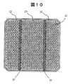
- Figure 9is a diagram showing a back surface Al electrode pattern example of n + -p-p ++ B / Al-BSF type solar cell applied to the present invention.
- FIG. 10is a diagram showing a back surface Al electrode pattern and back pad electrode Examples of n + -p-p ++ B / Al-BSF type solar cell applied to the present invention.
- Figure 11is a sectional structural diagram showing a cross section in the length direction of the front surface finger electrodes to be applied to n + -p-p ++ B / Al-BSF type solar battery cell of the present invention.
Landscapes
- Photovoltaic Devices (AREA)
Abstract
Description
Translated fromJapanese本発明は、シリコン太陽電池セル及びその製造方法に関する。The present invention relates to a silicon solar battery cell and a manufacturing method thereof.
まず、図1~図3を参照しながら、最も一般的なシリコン太陽電池セルであるn+−p−p+ Al−BSF形について説明する。当該形式の太陽電池セルは、図1にその断面説明図を示すように、p形シリコン基板1のおもて面にリン(P)拡散によって形成されたn+層2、裏面にアルミニュウム(Al)電極7の焼成によって形成されるp+層3を持った、いわゆる、n+−p−p+構造のシリコンに、おもて面(受光面)にパッシベーション酸化膜4、その上に反射防止膜であるシリコン窒化膜(SiNx)5が形成されており、更に、電気を取出すための電極として、おもて面電極6及び裏面電極7が形成されている。
おもて面電極6は、図2に示すように、フィンガー電極61とバスバー電極62で構成されるグリッド形(櫛形)電極で、その材質は銀(Ag)ある。一方、裏面電極7は、図3に示すように、裏面Al電極7と銀アルミニューム(AgAl)合金の裏面パッド電極8で構成される。これらの電極はスクリーン印刷・乾燥機にてペースト材を使用して印刷し、乾燥した後、焼成炉にて焼成することによって形成される。焼成はピーク温度740~780℃で行うが、裏面のほぼ全面に印刷したAlペースト中のAl原子が再結晶化時にシリコンに拡散して、裏面電界(Back Surface Field;BSFと略す)を発生するp+層3を形成する。このp+層3は、Al濃度は1018/cm3のオーダー、深さは4~5μmで、良好なBSFとなっている。
光照射によって発生した少数キャリアー(p形シリコンの場合は電子)の表面再結合速度を小さくするためのパッシベーション法としては、フッ酸(HF)溶液でリンガラス(以下、PSGという)膜をエッチングした後に、PE−CVD装置で受光面に反射防止膜となるSiNx膜5(膜厚約80nm)を形成する方法が一般的となっている。また、当該太陽電池セルは、前述のリン拡散時にリンゲッタリング及び電極焼成過程でAlゲッタリングが起こることから、シリコンバルク内での少数キャリアーのライフタイム向上が図られ、比較的高い性能(量産品での平均的変換効率は単結晶セルで16~17%程度、多結晶セルで15~16%程度)が得られる。このように、当該形式の太陽電池セルの製造方法は、非常に合理的な方法であるといえる。
しかし、当該形式の太陽電池セルでは、シリコン基板1を薄くした場合、電極焼成時の冷却過程でシリコン基板1と裏面のほぼ全面に形成される裏面Al電極7(焼成後膜厚15~20μm)との熱膨張係数の差から、セルの湾曲が発生し、割れやクラックによる歩留まりの低下が起こってくる。更に、肉眼では観察されないマイクロクラックの発生も出てくるが、モジュール化工程や供用中に、このマイクロクラックが顕在化して割れを引起こす結果ともなる。従って、シリコン基板1の薄形化には限界があり、実質上200μm程度となっている。なお、当該形式の太陽電池セルにおいて、上記の課題を解決する方法として、裏面全面にAl−BSF層を形成する代わりに、高膜厚の部分Al電極の焼成による部分Al−BSF層を形成した開発例(特許文献4)などもある。また、当該太陽電池セルの変換効率の向上にも限界があり、専ら、高価なプロセスでのテクスチャー構造の改良等に開発の重点が置かれているのが現状である。
次に、本発明と同一あるいは類似形式の太陽電池セルとして、p形またはn形シリコン基板の一方の面にリン拡散によるn+層、反対面にボロン(B)拡散によるp+層を形成したn+−p−p+構造またはp+−n−n+構造を有するシリコン形太陽電池セルについて説明する。
当該形式の太陽電池セルは、裏面もおもて面と同様なグリッド形電極とすることによって、両面からの受光によって発電する両面受光形太陽電池セルとなるものであり、1980年頃から多数の研究報告(非特許文献1、2)が行われてきたが、高ライフタイムを有する良質のシリコン基板が要求されること、その製造プロセスが複雑になること等の理由から、その量産は行われてこなかった。しかし、最近ではこの形式の両面受光形太陽電池セルの製造技術の改良及びその応用技術の開発が行われてきて、その量産(特許文献3、非特許文献3,4)も始まっている。ボロン拡散(p形基板の場合)またはリン拡散(n形基板の場合)によってBSFを形成する場合は、シリコン基板が薄くなっても湾曲は発生しないので160μm以下の薄形化も可能である。
当該形式の太陽電池セルでは、シリコン基板の片側面にリン拡散、反対面にボロン拡散を施す必要がある。このため、一旦、両面にボロン拡散を行い、一方のボロン拡散面にレジスト膜を形成して反対面の拡散層をアルカリ溶液やHF/HNO3溶液でエッチングする処理法等(特許文献2、非特許文献5)が採用されてきたが、製造プロセスが複雑になりコスト高となるという大きな課題がある。このため、低コスト化を目的に、図4に示すように、2枚のp(n)形シリコン基板1(16)を対向させてウェーハボート9に装荷して非対向面だけを拡散する対向拡散法(特許文献1、非特許文献5)が適用される場合もある。しかし当該拡散法では、図5に示すように、特に当該基板周辺部への廻り込み拡散11は避けられず、これが当該太陽電池セルの性能低下の大きな要因の一つとなっている。また、拡散ソースをシリコン基板の片面に塗布して、ベルト炉で拡散する方法や拡散ソースをシリコン基板に塗布して、横型炉に対向させて装荷して拡散する方法も使用されるが、ベルト接触面側の反対面や横型炉使用時の対向面には、やはりその周辺部への廻り込み拡散は発生する。更に、ベルト炉によるボロン拡散の場合は、シリコン基板内部への重金属、特に鉄(Fe)汚染が起こり、シリコン基板の少数キャリアーのライフタイムを著しく低下させるという欠点もある。
最初に説明したn+−p−p+ Al−BSF形太陽電池セルでは、裏面はほぼ全面がAl電極に覆われていること及び深いBSF層が形成されていることから、裏面での少数キャリアーの再結合は十分に抑制されている。一方、当該形式の太陽電池セルでは、おもて面に加えて、裏面での表面再結合速度を如何に低減するかが重要な課題となってくる。そのための表面パッシベーション法としては、ボロンガラス膜(以下、BSG膜という)及びPSG膜除去後に、直接あるいはパッシベーション酸化膜を付けてから、その両面にPE−CVDによるSiNx膜を形成よる方法(非特許文献参5)が一般的に行なわれている。しかし、更なる性能向上のためには、単純な量産プロセス技術での、より優れたパッシベーション法が課題となっている。
前述のように、裏面のほぼ全面にAl電極を持つn+−p−p+ Al−BSF形太陽電池セルでは、裏面電極のオーミック抵抗による損失は、おもて面グリッド電極による損失と比べて無視できる値となっている。一方、当該形式の太陽電池セルの電極は、一般的に、p+層側にAgAlのグリッド電極、n+層側にAgのグリッド電極とするので、その長所とは裏腹に、p+層側(p形基板使用時は裏受光面)の電極のオーミック抵抗(接触抵抗及び導体抵抗)による損失がかなり大きなものとなり、当該太陽電池セルの変換効率はその分だけ低くなるという課題がある。即ち、両面ともグリッド形電極とする場合、それらのオーミック抵抗を如何に低減するかが大きな課題の一つとなっている。
なお、当該太陽電池セルと類似形式の薄形片面受光太陽電池として、p型シリコン基板にボロン拡散及びリン拡散によってn+−p−p+構造を作製し、受光面(n+層側)にグリッド形電極を形成し、裏面(p+層側)は電極抵抗を従来のn+−p−p+ Al−BSF形並みとするため全面Al電極を印刷し、焼成後の反りを低減するために400℃の低温で焼成した開発例(特許文献2)がある。この場合、焼成温度は低くしているのでAlによるBSF形成は起こらない。
As shown in FIG. 2, the
As a passivation method for reducing the surface recombination rate of minority carriers (electrons in the case of p-type silicon) generated by light irradiation, a phosphor glass (hereinafter referred to as PSG) film was etched with a hydrofluoric acid (HF) solution. Later, a method of forming a SiNx film 5 (film thickness of about 80 nm) serving as an antireflection film on a light receiving surface with a PE-CVD apparatus has become common. In addition, since the solar cell undergoes Al gettering in the process of ring gettering and electrode firing during phosphorus diffusion described above, the lifetime of minority carriers in the silicon bulk is improved, and relatively high performance (quantity) The average conversion efficiency of the product is about 16 to 17% for the single crystal cell and about 15 to 16% for the polycrystalline cell). Thus, it can be said that the manufacturing method of the solar cell of the said format is a very rational method.
However, in the solar cell of this type, when the
Next, as a solar cell of the same or similar type as the present invention, an n+ layer by phosphorus diffusion is formed on one surface of a p-type or n-type silicon substrate, and a p+ layer by boron (B) diffusion is formed on the opposite surface. A silicon solar cell having an n+ -p+ structure or a p+ -n+ structure will be described.
The solar cell of this type is a double-sided solar cell that generates power by receiving light from both sides by making the back surface the same grid electrode as the front surface. Although reports (
In the solar cell of this type, it is necessary to perform phosphorus diffusion on one side of the silicon substrate and boron diffusion on the opposite side. For this reason, a treatment method or the like in which boron diffusion is once performed on both surfaces, a resist film is formed on one boron diffusion surface, and the diffusion layer on the opposite surface is etched with an alkali solution or an HF / HNO3 solution (
In the n+ -pp+ Al-BSF solar cell described first, the back surface is almost entirely covered with an Al electrode and a deep BSF layer is formed, so that minority carriers on the back surface are formed. The recombination of is sufficiently suppressed. On the other hand, in the solar cell of this type, how to reduce the surface recombination speed on the back surface in addition to the front surface is an important issue. As a surface passivation method for that purpose, a method of forming a SiNx film by PE-CVD on both sides directly or after attaching a passivation oxide film after removing the boron glass film (hereinafter referred to as BSG film) and the PSG film (non-non-conductive). Patent literature reference 5) is generally performed. However, in order to further improve the performance, a better passivation method using a simple mass production process technology has become an issue.
As described above, in an n+ -pp+ Al-BSF solar cell having an Al electrode on almost the entire back surface, the loss due to the ohmic resistance of the back surface electrode is larger than the loss due to the front grid electrode. It can be ignored. On the other hand, the electrode of the solar cell of the type generally grid electrode of AgAl the p+ layer side, since the grid electrodes of Ag on the n+ layer side, despite of its advantages, the p+ layer side There is a problem that the loss due to ohmic resistance (contact resistance and conductor resistance) of the electrode on the back light receiving surface (when a p-type substrate is used) becomes considerably large, and the conversion efficiency of the solar battery cell is lowered accordingly. That is, when grid electrodes are used on both surfaces, how to reduce their ohmic resistance is one of the major issues.
As thin single-sided light receiving solar cell similar format as the solar cells, to produce n+ -p-p+ structure by boron diffusion and phosphorus diffusion in the p-type silicon substrate, the light-receiving surface (n+ layer side) In order to reduce the warpage after firing by forming a grid electrode and printing the entire surface of the Al electrode so that the electrode resistance on the back surface (p+ layer side) is the same as the conventional n+ -pp+ Al-BSF type. In addition, there is a development example (Patent Document 2) which is fired at a low temperature of 400 ° C. In this case, since the firing temperature is low, BSF formation by Al does not occur.
シリコン太陽電池セルの製造コストはシリコン基板が70~75%を占めており、コスト低減のためにはシリコン基板の薄形化と変換効率の向上が不可欠である。一般的に普及しているn+−p−p+ Al−BSF形太陽電池セルでは薄形化は200μmが実質上の限界となっている。また、その量産ベースの変換効率は、ここ数年の間に向上してきているが、量産ベースの平均的変換効率は単結晶形で16~17%、多結晶形で15~16%程度である。本発明が解決しようとする課題は、更なるコスト低減を行うために、より薄形化(≦160μm)して高価なシリコンの使用量を軽減し、電極形成法として最も経済的なスクリーン印刷技術の適用を前提にした合理的なプロセスで、更に高効率化した片面受光形太陽電池セル及び両面受光形太陽電池セルを実現することである。Silicon substrates account for 70 to 75% of the manufacturing cost of silicon solar cells, and it is indispensable to reduce the thickness of the silicon substrate and improve conversion efficiency in order to reduce costs. In an n+ -pp+ Al-BSF solar cell that is generally spread, 200 μm is the practical limit for thinning. Moreover, the conversion efficiency based on mass production has improved over the past few years, but the average conversion efficiency based on mass production is about 16 to 17% for the single crystal form and about 15 to 16% for the polycrystalline form. . The problem to be solved by the present invention is that the most economical screen printing technique as an electrode forming method by reducing the thickness (≦ 160 μm) and reducing the amount of expensive silicon used for further cost reduction. It is to realize a single-sided light-receiving solar cell and a double-sided light-receiving solar cell that are more efficient by a rational process based on the application of the above.
本発明は、p形またはn形シリコン基板の片方の面にリン拡散によるn+層、反対面にボロン拡散によるp+を形成したn+−p−p+構造またはp+−n−n+構造を有するシリコン太陽電池セルの当該構造の製造方法において、第1ステップとして、ボロン拡散炉石英管内に2枚のシリコン基板を対向させて状態で装荷しておき、石英管内に拡散源の酸化硼素(B2O3)を導入してボロン拡散処理を行い、続いて酸素ガス(O2)を導入してボロン拡散に伴って拡散面に形成されるBSGをSiO2リッチの厚い膜に改質しておき、後述の第3ステップでのリン拡散時の廻込み拡散を抑止するマスク機能を高めておき、第2ステップとして、インライン式片面エッチング装置(ローラ式搬送系に基板を水平移動し、裏面側にフッ硝酸(HF/HNO3)溶液を当てる方式)を使用してフッ硝酸溶液にて対向面に生じた廻込み拡散及びシリコン酸化膜を除去し、第3ステップとして、拡散炉石英管内に上記処理したシリコン基板のボロン拡散面を対向させて装荷して石英管内に拡散源のP2O5を導入してリン拡散を行うが、またはリンソースを塗布してベルト炉でリン拡散を行うこと組合せたことを手段とする。
本発明は、ボロン拡散及びリン拡散によって形成されたn+−p−p+構造またはp+−n−n+構造を有するシリコン太陽電池セルの表面再結合の低減のためのパッシベーション法において、第一の手段として、拡散処理に伴って形成されたBSG膜及びPSG膜をフッ酸(HF)溶液で除去して純水洗浄した後、オゾン(O3)水に浸漬処理することによりシリコン基板表面に重金属汚染のない高品質の極薄シリコン酸化膜を形成し、第二の手段として、PE−CVD装置にてシリコン基板の両面に400~450℃の温度でシリコン窒化(SiNx)膜を形成することを組合せたことを手段とする。
本発明は、ボロン拡散及びリン拡散によって形成されたn+−p−p+構造またはp+−n−n+構造を有するシリコン太陽電池セルのボロン拡散面のグリッド形電極の形成方法において、まず、Al含有量2~4重量%のAgAlペーストを使用して、乾燥後膜厚8~10μmとなるグリッド形電極を印刷し、次に当該AgAl電極の上に、乾燥後膜厚24~26μmとなるように、Agペーストを重ね塗り印刷して乾燥した後に焼成することを手段とする。
本発明は、上記の手段で作製されるn+−p−p+構造のシリコン及び上記パッシベーション法を適用した、あるいは、同様な製造方法で製造される電極形成前のn+−p−p+構造を有するシリコン太陽電池セルにおいて、受光面(n+層側)にはグリッド形Ag電極、裏面にはAgAlパッド電極及び当該AgAlパッド電極部以外(但し、パッド電極はAl電極と接合するため両端0.5μmの重複部がある)のほぼ全面に均一に、又は、多数の小さな開口部を有するパターンで、焼成後厚さ6~8μm(従来のn+−p−p+ Al−BSF形の50%以下の膜厚)となる薄いAl電極を印刷し、焼成することによって、当該Al電極が覆った部分にB及びAlの拡散した強いBSF層となるp++層を形成することを手段とする。The present invention, p-type orn + layer by phosphorus diffusion on one surface of the n-type silicon substrate,n +-p-p + structure was formedp + by boron diffusion into the opposite surface orp +-n-n + In the method for manufacturing a silicon solar cell having a structure, as a first step, two silicon substrates are loaded facing each other in a boron diffusion furnace quartz tube, and boron oxide as a diffusion source is placed in the quartz tube. Boron diffusion treatment is performed by introducing (B2 O3 ), and then oxygen gas (O2 ) is introduced to reform the BSG formed on the diffusion surface along with boron diffusion into a thick SiO2 rich film. In addition, the mask function for suppressing the wraparound diffusion at the time of phosphorus diffusion in the third step which will be described later is enhanced, and as the second step, the in-line type single-side etching apparatus (the substrate is moved horizontally to the roller type transport system, On the back side Tsu nitrate (HF / HNO3) solution using the method) shed removing diffusion and silicon oxide film sneak generated on the facing surface in hydrofluoric-nitric acid solution, as a third step, the process in a diffusion furnace quartz tube combinations to perform the boron diffusion surface of the silicon substrate is loaded by the counter performs phosphorus diffusion by introducing P2 O5 of the diffusion source into the quartz tube, but or by coating a phosphorus source phosphoric diffusion in a belt furnace That means.
The present invention provides a passivation process for the reduction of surface recombination of the silicon solar cell having the n+ -p-p+ structure, or p+ -n-n+ structure formed by boron diffusion and phosphorus diffusion, the As one means, after removing the BSG film and PSG film formed by the diffusion treatment with a hydrofluoric acid (HF) solution and washing with pure water, the silicon substrate surface is immersed in ozone (O3 ) water. A high quality ultrathin silicon oxide film free from heavy metal contamination is formed on the substrate, and as a second means, a silicon nitride (SiNx ) film is formed on both surfaces of the silicon substrate at a temperature of 400 to 450 ° C. using a PE-CVD apparatus. It is a means to combine to do.
The present invention provides a method of forming a grid-shaped electrode of the boron diffusion surface of the silicon solar cell having the n+ -p-p+ structure, or p+ -n-n+ structure formed by boron diffusion and phosphorus diffusion, first A grid electrode having a film thickness of 8 to 10 μm after drying was printed using an AgAl paste having an Al content of 2 to 4% by weight, and then a film thickness of 24 to 26 μm after drying was formed on the AgAl electrode. In this way, the Ag paste is baked after being overcoated, dried, and dried.
The present invention was applied to silicon and the passivation method of the n+ -p-p+ structure fabricated by the above-mentioned means, or the front electrode formation which are produced by a production method similar to n+ -p-p+ In a silicon solar cell having a structure, a grid-shaped Ag electrode is provided on the light receiving surface (n+ layer side), and the AgAl pad electrode and the AgAl pad electrode portion other than the AgAl pad electrode portion are provided on the back surface. Uniform on almost the entire surface of 0.5 μm overlap, or a pattern having many small openings, and a thickness of 6 to 8 μm after firing (conventional n+ -pp+ Al-BSF type A thin Al electrode having a thickness of 50% or less) is printed and baked to form a p++ layer that becomes a strong BSF layer in which B and Al are diffused in a portion covered by the Al electrode; You .
本発明によれば、厚さ160μm以下の薄形で、且つ高効率のn+−p−p+ B−BSF形またはp+−n−n+ P−BSF形太陽電池セル(両面受光形)を低コストで実現できる。また、従来形のn+−p−p+ Al−BSF形では達成できない、厚さ160μm以下の薄形で、且つ18%以上の高効率の新しい形式であるn+−p−p++ B/Al−BSF形片面受光太陽電池セルが低コストで実現できる。
本発明によれば、上述のn+−p−p+ B−BSF形またはp+−n−n+ P−BSF形の両面受光太陽電池セル及びn+−p−p++ B/Al−BSF形片面受光太陽電池セルが、消耗品である印刷機のスクリーンマスクの交換だけで、同一の製造設備で製造できるという効果がある。
本発明では、ボロン拡散及びリン拡散の順序で不純物熱拡散を行い、ボロン拡散には石英管方式の横型炉での対向拡散法を採用し、リン拡散には石英管方式の横型炉での対向拡散法またはベルト炉による拡散法を採用し、且つ、ボロン拡散後に酸素ガスを導入して生成されたBSG膜をSiO2リッチに改質しておき、その後のリン拡散時の廻込み拡散抑制のマスク機能を強化すること、及びボロン拡散後に廻込み拡散の生じた反対面を片面エッチング装置にて効率的にフッ硝酸溶液でエッチングした後にリン拡散を行うことによって、漏洩電流の少ない高品質のn+−p−p+またはp+−n−n+構造を経済的に作製できるという効果がある。
本発明では、上述のn+−p−p+またはp+−n−n+構造を作製した後に、BSG膜及びPSG膜除去後の洗浄時にオゾン水に浸漬を行うことによって重金属汚染のない高品質の極薄酸化膜を形成し、その上に酸化炉によるパッシベーション酸化膜を形成し(割愛の場合ある)、更にPE−CVDにより400~450℃で太陽電池セルの両面にSiNx膜を形成して電極焼成炉にて焼成するという複合的な表面パッシベーション方法によって、太陽電池セルの両面での少数キャリアー表面再結合速度を低減し、高効率化できるという効果がある。
本発明では、n+−p−p+ B−BSF形またはp+−n−n+ P−BSF形セルのp+層側電極形成において、まず乾燥後膜厚10~15μm、望ましくは10~12μm、Al含有量2~4重量%のAgAl電極を印刷・乾燥し、その上に乾燥後膜厚20~24μmのAg電極を印刷・乾燥した後、同時焼成することにより、p+層と良好なコンタクトをとる薄いAgAl電極層とAgAl電極より抵抗率の小さい(約60%)厚いAg電極層を重ねた2層構造の接触抵抗及び導体抵抗の小さい厚膜電極を実現できるので、当該電極によるオーミック抵抗損失を低減でき、より変換効率の高い両面受光太陽電池セルが得られるという効果がある。
本発明では、前述のボロン拡散及びリン拡散で作製した高品質のn+−p−p+構造を有するシリコン処理基板に、BSG及びPSGの除去後にオゾン水浸漬による重金属汚染のない良質の極薄酸化膜形成し、更に酸化炉によるパッシベーション酸化膜及びPE−CVDによるSiNx膜形成を形成するという複合的な両面の表面パッシベーション処理を行うこと、裏面(p+)側の電極として、そのほぼ全面に均一に、あるいは、多数の小さな開口部を有するパターンで、膜厚6~10μmの薄いAl電極を形成することによって、薄形で高効率の新しい形式のn+−p−p++ B/Al−BSF形セルが実現できる。当該太陽電池セルは、厚さを160μm以下に薄くしても、Al電極が薄いこと及び電極焼成後の冷却時のAl電極の縮退をその多数の開口部で吸収するので、当該太陽電池セルの湾曲は十分抑制され、且つ裏面電極の抵抗が殆ど無視可能な値になること、当該Al電極部にBに加えてAlの拡散した深いp++層の強いBSFが形成されること、更に当該Al電極部に到達する長波長成分の光を反射させる機能を持つことから、前述した従来形のn+−p−p+ Al−BSF形では実現できない高効率の薄形太陽電池セルが低コストで実現できるという効果がある。According to the present invention, a thin and high-efficiency n+ -pp+ B-BSF type or p+ -n+ P-BSF type solar cell (double-sided light receiving type) having a thickness of 160 μm or less Can be realized at low cost. Furthermore, it can not be achieved with conventional form ofn + -p-p + Al- BSF type, the following thin thickness 160 .mu.m, and a new format of 18% or more efficiencyn +-p-p ++ B / An Al—BSF single-sided photovoltaic cell can be realized at low cost.
According to the present invention, the above-mentioned n+ -p+ B-BSF type or p+ -n+ P-BSF type double-sided light-receiving solar cell and n+ -p+++ B / Al-BSF There is an effect that the single-sided light-receiving solar battery cell can be manufactured with the same manufacturing equipment only by replacing the screen mask of the printing press, which is a consumable item.
In the present invention, impurity thermal diffusion is performed in the order of boron diffusion and phosphorus diffusion, and a counter diffusion method in a quartz tube type horizontal furnace is adopted for boron diffusion, and an opposing diffusion method in a quartz tube type horizontal furnace is adopted for phosphorus diffusion. A diffusion method or a diffusion method using a belt furnace is adopted, and a BSG film formed by introducing oxygen gas after boron diffusion is modified to be rich in SiO2 , thereby suppressing wraparound diffusion during subsequent phosphorus diffusion. High-quality n with less leakage current by strengthening the mask function and performing phosphorous diffusion after etching the opposite surface where wraparound diffusion occurs after boron diffusion efficiently with a single-sided etching apparatus. There is an effect that a+ −p−p+ or a p+ −n−n+ structure can be produced economically.
In the present invention, after the above-described n+ -pp+ or p+ -nn+ structure is produced, immersion in ozone water is performed at the time of cleaning after removing the BSG film and the PSG film. A quality ultra-thin oxide film is formed, a passivation oxide film is formed on the oxidation furnace on the oxide film (may be omitted), and a SiNx film is formed on both sides of the solar cell at 400 to 450 ° C. by PE-CVD. Thus, the composite surface passivation method of firing in an electrode firing furnace has the effect of reducing the minority carrier surface recombination speed on both sides of the solar battery cell and increasing the efficiency.
In the present invention, in the formation of the p+ layer side electrode of the n+ -pp+ B-BSF type cell or the p+ -n+ P -BSF type cell, first, after drying, the film thickness is 10 to 15 μm, preferably 10 to 10 μm. Print and dry an AgAl electrode with 12 μm and Al content of 2 to 4% by weight, and after drying, print and dry an Ag electrode with a film thickness of 20 to 24 μm on it, and then co-firing to make it good as p+ layer A thick film electrode having a low contact resistance and a low conductor resistance can be realized by laminating a thin AgAl electrode layer having a good contact and a thick Ag electrode layer having a resistivity lower than that of the AgAl electrode (about 60%). The ohmic resistance loss can be reduced, and there is an effect that a double-sided light receiving solar cell with higher conversion efficiency can be obtained.
In the present invention, a high-quality ultrathin material free from heavy metal contamination due to ozone water immersion after removal of BSG and PSG on a silicon-treated substrate having a high-quality n+ -pp+ structure prepared by boron diffusion and phosphorus diffusion described above. A composite double-sided surface passivation treatment is performed, in which an oxide film is formed, and a passivation oxide film by an oxidation furnace and a SiNx film formation by PE-CVD are formed. As an electrode on the back surface (p+ ) side, almost the entire surface is formed. By forming a thin Al electrode having a film thickness of 6 to 10 μm uniformly or in a pattern having a large number of small openings, a thin and highly efficient new type of n+ -pp++ B / Al- A BSF type cell can be realized. Even if the solar cell is thinned to 160 μm or less, the Al electrode absorbs the thinness of the Al electrode and the degeneration of the Al electrode during cooling after firing the electrode. Bending is sufficiently suppressed and the resistance of the back electrode becomes a negligible value, and a strong BSF of a deep p++ layer in which Al is diffused in addition to B is formed in the Al electrode portion. Since it has a function of reflecting light having a long wavelength component that reaches the electrode part, a high-efficiency thin solar cell that cannot be realized by the conventional n+ -pp+ Al-BSF type described above at low cost. There is an effect that it can be realized.
本発明の実施例1として、まず、図6(a)を参照しながら、p形シリコン基板を使用したn+−p−p+ B−BSF形太陽電池セルの構造について説明する。なお、n形シリコン基板を使用したp+−n−n+ P−BSF形太陽電池セルの構造は同図(b)に示すが、同様な説明となるので割愛する。
本発明を適用する太陽電池セルは、p形シリコン基板1のおもて面にリン拡散よって形成されたn+層2と裏面にボロン拡散によって形成されたp+層12を有している、いわゆる、n+−p−p+構造となっている。ここで、n+−p接合はダイオードを形成しており、p−p+接合はBSFを形成している。p形シリコン基板1のおもて面には、シリコン酸化膜(SiO2)4とその上にSiNx膜5が形成されており、裏面側には同じくシリコン酸化膜13とSiNx膜14が形成されている。
当該太陽電池セルで発生する電気を取り出すために、おもて面にはグリッド形Ag電極6が、裏面には膜厚7~9μmの裏面第1層AgAl電極151と膜厚15~18μmの裏面第2層Ag電極152が2層構成となった裏面グリッド電極15が形成されている。当該太陽電池セルは両面ともグリッド形電極となっているので、両面からの光照射で発電ができる両面受光太陽電池セルであり、また、裏面グリッド電極のフィンガーの幅拡大、本数の増加を行って抵抗を小さくした片面受光形太陽電池セルにすることもできる。本太陽電池セルは、従来のn+−p−p+ Al−BSF形太陽電池セルのような裏面全面に形成されるAl電極7(図3)がないため、160μm以下の薄形が実現できる。
一方、従来のn+−p−p+ Al−BSF形セルでは裏面電極のオーミック抵抗による損失はおもて面電極のそれに比べて無視できる値となるが、当該太陽電池セルでは裏面にも、図2に示すような、グリッド形電極を採用しているので、その損失が大きくなり、その分、おもて面入射時のセル変換効率が低くなるという短所がある。本発明では、裏面電極は、まず、ボロン拡散によるp+層12との良好なコンタクト(接触抵抗の低減)を取るため、乾燥後膜厚が10~15μm、望ましくは10~12μmとなるAl含有量2~4重量%のAgAlペーストを印刷して、その上に抵抗率が低く(AgはAgAl合金の約60%)且つ半田濡れ性の優れたAgペーストを乾燥後膜厚20~24μmで重ね塗り印刷して焼成した高膜厚の2層構成裏面グリッド形電極15とすることによって、当該電極によるオーミック抵抗損失を低減している。
なお、従来、p+層側に形成するAgAl電極は、モジュール化時のインターコネクションリボン電線の半田付けを行う際の半田濡れ性の観点からAl含有量は2%以下に抑えられていたが、本発明では、裏面第2層Agグリッド形電極152でより良好な半田濡れ性を確保するとともに、裏面第1層AgAlグリッド形電極151はボロン拡散によるp+層12とのより良好なコンタクトをとれるように、Al含有量を2~4重量%に引き上げているという特徴がある。更に、従来のp+層側のAgAl電極の膜厚は15~20μmであるが、重ね刷り印刷により、全膜厚は23~27μmと厚くして、導体抵抗を低減している。
以上、本発明を適用した実施例1の太陽電池セルの構造上からの説明と特徴について述べたが、以下、図7を参照しながら、製造プロセス面から説明する。
本発明を適用するボロン拡散層を有するシリコン太陽電池セルは、下記のプロセス処理にて製造する。なお、当該太陽電池セルは両面受光形とするので、シリコン基板は少数キャリアーのライフタイムは100μs以上が望ましく、従って、その比抵抗は3~8Ω・cmと高いものを使用する。
(1)ダメージ層除去とテクスチャーエッチング:高濃度アルカリ(NaOHまたはKOH)溶液によるシリコン基板のダメージ層除去した後、単結晶基板の場合は低濃度のアルカリ溶液(添加材含む)でランダムピラミッド形のテクスチャー、多結晶基板の場合はアルカリまたは酸によるテクスチャーの形成を行う。単結晶シリコン基板でのピラミッド状テクスチャーでは、主たるピラミッドの高さは2~5μmで、反射率は9~10%(波長800nmにて)となる。一方、多結晶のテクスチャーでは深さは約0.5μmと浅く、反射率は20~25%(波長800nmにて)となる。
(2)ボロン拡散:前述し、図4に示すように、2枚のシリコン基板1を対向させてウェーハボート12に詰め、横型BBr3拡散炉に挿入して、拡散温度910℃~930℃で、3臭化硼素(BBr3)、N2キャリアーガス及びO2ガスを導入してシート抵抗65~80Ω/□のボロン拡散を行う。拡散終了でBBr3ガスの供給を停止し、10~20分のアフターパージ及びボロン(B)の拡散プロファイル(深さ方向の不純物濃度分布)を調整するためのドライブ処理を行う。引き続いて、O2ガス供給量を増加させて、シリコン基板1の表面に形成されたBSG膜10をSiO2リッチに改質して膜厚85~95nmとする。このBSG改質の目的は、改質されたBSG膜10が後述のプロセス(4)の対向リン拡散(または、ベルト式拡散炉での拡散)時に対向面(または、ベルト接触面)へのリンの廻り込み拡散を抑制するマスクの効果を持たせるためである。リン拡散のマスクとするSiO2膜の必要な厚さは、後述のリン拡散温度と拡散時間では約60nmであるが、BSG膜10はポーラスであり、そのままではリンの廻込み拡散が起こってしまうが、改質したBSG10はシリコン基板1の廻込み拡散に対するマスク効果を十分果たすことができる。なお、ボロン拡散は他の液体ソース3臭化塩素(BCl3)や固体ソースの窒化硼素(BN)でも良い。
(3)おもて面エッチング:プロセス(2)のボロン拡散では、対向面への廻り込み拡散の僅少化を図るため種々の手段が講じられるが、前述のようにシリコン基板1の周辺部に幅1~3mmの廻込み拡散による薄いBSGによる変色部11が生じるとともに、その内側に端部から4~8mmの近辺まで有為な電気的性能が低下する領域ができることは避けられない。更に、シリコン基板1は拡散炉から取出す過程及び炉外に出した時は高温状態で空気に晒されるため、その対向面にもある程度の酸化が生じてシリコン酸化膜(SiO2)ができる。このボロンの廻り込み拡散及びシリコン酸化膜のある状態でリン拡散を行ってn+−p接合をつくると、この接合(ダイオード)はかなりの漏洩電流を生むばかりでなく、電極形成時に太陽電池セルのシャント分抵抗となるポテンシャルが出てくる。
片面エッチングの方法は種々あるが、本発明では最も経済的なプロセスとして、最近、ドイツ国Schmid社やRENA社等が開発・販売しているような、インライン式片面エッチング装置(ローラ式搬送系に基板を水平移動し、裏面側にHF/HNO3溶液を当てる方式)を適用することを特徴とする。本装置を使用して、おもて面だけを比較的低濃度のHF/HNO3溶液(49%HF:65%HNO3:DIW=1:1:5~10)で0.2~0.4μmエッチングする。BSG膜10は吸湿性を有するが、SiO2リッチに改質したBSG膜は十分な耐湿性能を持つという効果もある。
(4)リン拡散:ボロン拡散処理をしたシリコン基板1を、ボロン拡散面を対向させてウェーハボート9に詰めて横型POCl3拡散炉に挿入して、拡散温度850~880℃、拡散時間35~40分で、リン拡散を行う。おもて面エッチングを行わない場合は、周辺部にボロンの廻り込み拡散が発生するため、リン拡散深さまでn形特性を保つためにB密度を超えるP密度とする必要がありシート抵抗は低め(40~45Ω/□)とせざるを得ない。しかし、上記の片面エッチングで廻込み拡散は適切にエッチングされるので、良好なセル特性を得る高めのシート抵抗(60Ω/□以上)での拡散が可能となる。また、対向面(ベルト炉の場合はベルト接触面)のボロン拡散面は改質BSG膜10で保護されるのでリンの廻り込み拡散は大幅に抑制できる。更にシリコン基板1の当該面のSiO2膜も除去しているので、良好な拡散性能が得られ、n+−p接合近辺の酸素原子の低減も図られる。
(5)BSG/PSG除去とオゾン洗浄:ウェットステーションを使用して、5%HF溶液にてBSG膜及びPSG膜の除去と純水洗浄を行った後、最終段の槽で、濃度10~15ppmのオゾン(O3)溶液に浸漬してシリコン基板1の表面の洗浄及び重金属汚染のない高品質の20~30Åの極薄シリコン酸化膜を形成する。重金属汚染は太陽電池セルの再結合中心となって、キャリアーの表面再結合速度を大きくする要因となっているものであり、BSG/PSG除去と同時に高品質のシリコン酸化膜を形成することによって、後続のプロセスでの汚染要因の影響をも僅少化できるものである。
(6)接合分離:コインスタック状に前記基板1をマガジンに詰めてプラズマエッチャー(CF4ガス使用)にて基板端部を50~100μmエッチングして接合分離を行う。なお、当該接合分離は、プロセス(5)のBSG/PSG除去とオゾン洗浄前に行っても良いし、また、後述のプロセス(10)の電極焼成後にレーザスクライバーで行っても良い。
(7)SiNx膜形成:プラズマをシリコン基板の上部に発生させるプロセスチェンバーとシリコン基板の下部に発生させるプロセスチェンバーを有するダブルチェンバー方式のPE−CVDにて、400℃~450℃で当該シリコン基板1の両面にSiNx膜5、14を成膜する。当該SiNx膜5、14は、厚さ75~85nm、屈折率2.1~2.3とすることによって、反射率は単結晶基板で波長800nmにおいて1~3%、多結晶基板で6~10%が得られる。当該SiNx膜5、14は反射防止膜機能の他、成膜時及びその後の電極焼成時に当該膜中の水素原子の働きで太陽電池セルの表面パッシベーション(多結晶シリコン基板の場合はバルクパッシベーション効果もある)が起こることが良く知られている。前述のプロセス(5)でのシリコン基板1の表面に高品質のSiO2膜4、13を形成している効果と相俟って良好なパッシベーション効果を上げるものである。
(8)おもて面電極形成:太陽電池セルの性能を上げるためには、フィンガー電極61(図2)の幅は95~100μmと細くして電極の影による損失を減らすとともに、そのオーミック抵抗を減らすために膜厚は大きくする必要がある。一般的には1回の印刷で行うが、この場合は、その焼成後膜厚は一般的には15~18μmの範囲となる。従って、高膜厚を実現するために、印刷・乾燥装置は画像認識装置付の高精度位置決め機能を有する2段構成の印刷・乾燥装置を適用して、まず、1段目印刷乾燥装置でおもて面Agグリッド形電極6(フィンガー電極61とバスバー電極62より構成)を印刷乾燥し、続いて、2段目印刷乾燥装置を使用して、重ね塗りで印刷乾燥し、乾燥後膜厚が34~36μmの高膜厚なものとする。プロセス(10)の焼成で、ペースト中のバインダーが飛散して焼締まりが起こり、焼成後膜厚は乾燥後膜厚の75~80%になるので、焼成後膜厚は25μm以上が確保できる。
(9)裏面電極形成:当該太陽電池セルは両面受光形であり、裏面電極は、おもて面電極と同様に、グリッド形電極(図2)とする。裏面電極形成用の印刷・乾燥装置は2段構成として、初段の印刷・乾燥機で乾燥後膜厚10~15μm、望ましくは10~12μmの薄いAgAl電極151を印刷・乾燥した後、第2段の印刷・乾燥機でその上に乾燥後膜厚20~24μmのAg電極152を重ね刷り印刷する。後述のプロセス(10)の焼成により、焼成後膜厚は23~27μmを得るようにする。
本発明では、p+層12への良好なコンタクト(接触抵抗の低減)を確保するため第1層はAl含有量2~4重量%のAgAl電極としている。一方、AgAl電極は合金であるためその抵抗率は6.0μΩcm程度と高くなるので導体抵抗は大きくなる。従って、フィンガー電極61の導体抵抗を小さくするため、第1層AgAlグリッド形電極151は焼成後膜厚で10~15μm、望ましくは10~12μmと薄くして、その上の第2層に抵抗率が約3.6μΩcmである第2層Agグリッド形電極152を焼成後膜厚20~24μmと厚くして2層構成の厚膜の電極とすることによって導体抵抗の低減を図ったものである。
また、本発明では、裏面第2層Agグリッド形電極152はAg電極としているので、半田付け性能は良好となり、モジュール化時のインターコネクションリボン電線の半田付けが容易となるので薄形セルの割れのポテンシャルを低減している。なお、従来のAgAl電極は、半田濡れ性が保てるAl含有量として1~2重量%としている。
当該太陽電池セルを両面受光形として製作する場合は、裏面も受光面となるので、フィンガー電極の設計はおもて面電極と同等な幅とする。一方、当該太陽電池セルを片面受光形とする場合は、裏面電極の影による光損失は考える必要がないので、フィンガー幅は少し大きくし、且つ、本数は多くすることによってオーミック抵抗を低減する。また、片面受光形では、p形シリコン基板1の少数キャリアーのライフタイムは10μs以下で良いので、その比抵抗は1~3Ω・cmと低いものとすることができ、抵抗による損失は更に小さくすることができる。
(10)電極焼成:シリコン酸化膜4、13及びSiNx膜5、14をファイアースルーして、且つ、n+層及びp+層を突き抜けず良好なコンタクトを実現するために、ピーク温度750~780℃の急峻な温度プロファイルで両面の電極を同時に焼成する。この焼成過程で、前述のSiNx膜5,14中の水素が更にパッシベーションを進展させる効果がある。As Example 1 of the present invention, first, a structure of an n+ -pp+ B-BSF solar cell using a p-type silicon substrate will be described with reference to FIG. In addition, although the structure of the p<+> -n+ P-BSF type | mold solar cell using an n-type silicon substrate is shown in the figure (b), since it becomes the same description, it omits.
The solar cell to which the present invention is applied has an n+ layer 2 formed by phosphorus diffusion on the front surface of the p-
In order to take out electricity generated in the solar cell, the grid-shaped
On the other hand, in the conventional n+ -pp+ Al-BSF type cell, the loss due to the ohmic resistance of the back surface electrode is negligible compared to that of the front surface electrode. Since the grid-type electrode as shown in FIG. 2 is adopted, the loss increases, and there is a disadvantage that the cell conversion efficiency at the front surface incidence is reduced accordingly. In the present invention, the back electrode is first Al-containing so that the film thickness after drying is 10 to 15 μm, preferably 10 to 12 μm, in order to obtain good contact (reduction of contact resistance) with the p+ layer 12 by boron diffusion. An AgAl paste of 2 to 4% by weight is printed, and an Ag paste with low resistivity (Ag is about 60% of the AgAl alloy) and excellent solder wettability is dried on it and stacked with a film thickness of 20 to 24 μm. By forming the two-layered
Conventionally, the AgAl electrode formed on the p+ layer side has been suppressed to an Al content of 2% or less from the viewpoint of solder wettability when soldering an interconnection ribbon electric wire during modularization. in the present invention, while securing the better the solder wettability on the back second layer Ag grid-shaped
As mentioned above, although the description from the structure of the photovoltaic cell of Example 1 to which this invention was applied and the characteristic were described, it demonstrates from a manufacturing process surface hereafter, referring FIG.
A silicon solar battery cell having a boron diffusion layer to which the present invention is applied is manufactured by the following process. Since the solar cell is a double-sided light receiving type, it is desirable that the silicon substrate has a minority carrier lifetime of 100 μs or more. Therefore, a silicon substrate having a high specific resistance of 3 to 8 Ω · cm is used.
(1) Damage layer removal and texture etching: After removing the damage layer of the silicon substrate with a high concentration alkali (NaOH or KOH) solution, in the case of a single crystal substrate, a random pyramid shape with a low concentration alkali solution (including additives) In the case of a textured or polycrystalline substrate, the texture is formed with alkali or acid. In the pyramidal texture on the single crystal silicon substrate, the main pyramid has a height of 2 to 5 μm and a reflectance of 9 to 10% (at a wavelength of 800 nm). On the other hand, the polycrystalline texture has a shallow depth of about 0.5 μm and a reflectance of 20 to 25% (at a wavelength of 800 nm).
(2) Boron diffusion: As described above and shown in FIG. 4, the two
(3) Front surface etching: In the boron diffusion in the process (2), various measures are taken in order to minimize the diffusion around the opposing surface. It is inevitable that a
There are various methods for single-sided etching. However, as the most economical process in the present invention, an in-line type single-sided etching apparatus (roller type transfer system) recently developed and sold by German company Schmid, RENA, etc. A method of horizontally moving the substrate and applying a HF / HNO3 solution to the back surface side) is applied. Using this apparatus, only the front surface is 0.2 to 0. 0 with a relatively low concentration HF / HNO3 solution (49% HF: 65% HNO3 : DIW = 1: 1: 5 to 10).
(4) Phosphorus diffusion: The
(5) BSG / PSG removal and ozone cleaning: Use a wet station to remove the BSG film and PSG film with 5% HF solution and clean with pure water. A surface of the
(6) Bonding separation: The
(7) SiNx film forming: plasma at PE-CVD double chamber system having a process chamber to generate at the bottom of the process chamber and the silicon substrate to generate the upper portion of the silicon substrate, the silicon substrate at 400 ° C. ~ 450 ° C. SiNx films 5 and 14 are formed on both sides of the
(8) Front surface electrode formation: In order to improve the performance of the solar battery cell, the finger electrode 61 (FIG. 2) is thinned to 95 to 100 μm to reduce the loss due to the shadow of the electrode, and its ohmic resistance In order to reduce the film thickness, it is necessary to increase the film thickness. Generally, printing is performed once. In this case, the film thickness after firing is generally in the range of 15 to 18 μm. Therefore, in order to realize a high film thickness, the printing / drying device is a two-stage printing / drying device having a high-precision positioning function with an image recognition device. The front surface Ag grid-type electrode 6 (comprised of
(9) Back electrode formation: The solar battery cell is a double-sided light receiving type, and the back electrode is a grid electrode (FIG. 2) as in the case of the front surface electrode. The printing / drying apparatus for forming the back electrode has a two-stage configuration. After printing / drying the
In the present invention, the first layer is an AgAl electrode having an Al content of 2 to 4% by weight in order to ensure good contact (reduction in contact resistance) to the p+ layer 12. On the other hand, since the AgAl electrode is an alloy, its resistivity is as high as about 6.0 μΩcm, so that the conductor resistance is increased. Therefore, in order to reduce the conductor resistance of the
Further, in the present invention, since the back surface second layer
When the solar cell is manufactured as a double-sided light receiving type, the back surface is also a light receiving surface, so the finger electrode is designed to have the same width as the front surface electrode. On the other hand, when the solar cell is a single-sided light receiving type, it is not necessary to consider the light loss due to the shadow of the back electrode, so the finger width is slightly increased and the ohmic resistance is reduced by increasing the number. In the single-sided light receiving type, since the lifetime of minority carriers of the p-
(10) Electrode firing: In order to realize a good contact without fire through the
本発明の実施例2として、前記のn+−p−p+構造のシリコン基板をベースとした薄形高効率の新しい形式であるn+−p−p++ B/Al−BSF形太陽電池セルの構造について、図8~11を参照しながら説明する。
当該太陽電池セルは、図8にその断面構造説明図を示すように、p形シリコン基板1のおもて面側にリン拡散によるn+層2、裏面側にボロン拡散によるp+層12及び、図8、10に示すように、多数の小さな開口部21を有して、裏面AgAlパッド電極22以外の裏面のほぼ全面に形成される裏面Al電極20が覆ったシリコン部分に当該Al電極20の焼成に伴って形成されるBとAlによるp++層19を有している。この処理されたシリコン基板1のおもて面にはSiO2膜4と更にその上にSiNx膜5が形成されており、裏面には同じくSiO2膜13とSiNx膜14が形成されている。電極は、おもて面にはグリッド形Ag電極6、裏側には前記の裏面Al電極20及び裏面AgAlパッド電極22が形成されている。
おもて面フィンガー電極の長さ方向での断面説明図である図11を使用して当該太陽電池セルの電極構成を説明する。おもて面グリッド形電極6(フィンガー電極61とバスバー電極62から構成)は実施例1と同様に2回重ね塗り印刷によって膜厚は25μm以上としている。一方、裏面電極は、第1の印刷乾燥装置によって印刷した、焼成後膜厚6~15μm、望ましくは6~10μmの多数の小さな開口部を有する裏面Al電極20と、第2の印刷乾燥装置によって印刷した焼成後膜厚18~22μmの裏面パッド電極22から構成されている。
次に、当該太陽電池セルをその製造プロセス面から、前述の図7及び図9~11を参照しながら詳細に説明する。
当該太陽電池セルは、前記の実施例1のn+−p−p+ B−BSF形太陽電池セルのプロセス(8)おもて面電極印刷・乾燥までは全く同じプロセスで製造される。但し、当該太陽電池セルは片面受光セルであるので、使用するシリコン基板の少数キャリア(電子)のライフタイムは短くてよいので、その比抵抗は1.0~4.0Ω・cmとすることによって、太陽電池セルのシリコンバルク部の抵抗を低減する。
プロセス(9)裏面電極印刷乾燥では、まず第1の印刷・乾燥装置で、図9にそのパターン例を示すように、多数の小さな開口部21を有した裏面Al電極20を乾燥後膜厚8~12μmの薄い膜厚で印刷・乾燥する。本実施例では、開口部は直径1.5~2.5mm円形としたが、開口部の形状は必ずしも円形である必要はない。前述したように、単結晶シリコン基板の場合はテクスチャーのピラミッドの高さが3~5μmであるので、これをカバーする膜厚とし、焼成後膜厚6~10μm(単結晶のn+−p−p+ Al−BSF形太陽電池セルでは15~20μm)、即ち、焼成前膜厚8~12μmで形成する。なお、多結晶シリコン基板の場合はテクスチャーの深さが浅いので焼成後膜厚は更に小さくすることができる。次に第2の印刷・乾燥装置で、図10に示すように、裏面AgAlパッド電極22を裏面Al電極20と0.4~0.6mm重ねた幅で、乾燥後膜厚18~22μmで印刷・乾燥する。
ステップ(10)では、ピーク温度750~780℃の急峻な温度プロファイルで両面の電極を同時に焼成する。この焼成によって、おもて面グリッド形電極6はSiNx膜及びSiO2膜をファイアースルーして焼き締められ、膜厚は乾燥後膜厚の75~80%になる。また、裏面Al電極20及び裏面パッド電極22は焼成過程で、図8及び図11に示すように、当該裏面Al電極20に覆われた部分のシリコン基板には、ボロン拡散によるp+層12の上に、更にAl原子が拡散した深いp++層19が形成され、強力なBSF層となる。また、裏面Al電極20の焼成に伴い太陽電池セルの活性領域であるシリコンバルク内の結晶格子間に入り込んだ重金属(特にFe)をp++層19と当該裏面Al電極20の界面にゲッタリングし、少数キャリアーのライフタイムを向上させる。更に、両面に成膜したSiNx膜5、14の中に含まれる水素の効果で両面の表面パッシベーション及び多結晶基板の場合はバルクパッシベーションが進展する。なお、裏面Al電極20の焼成で、前述のp++層19の上にSiAl合金層ができ、長波長成分の光をシリコン内部へ反射する効果も出てくる。
本実施例2の太陽電池セル特有のBとAlによるp++層19について少し考察してみる。拡散温度910~930℃でのボロン拡散(ドライブイン処理含む)によるp+層12の深さは凡そ0.4μmで、表面近傍のB濃度は凡そ1×10²⁰atoms/cm3である。一方、n+−p−p+ Al−BSF形セルでのAl電極印刷・焼成によるp+層3(図1)は、電極印刷・焼成時のAlペーストの組成及び膜厚、焼成温度パターンに影響されるが、n+−p−p+ Al−BSF形セルでの一般的な条件、即ち、Al電極7(図1)の焼成前厚さ20~25μm、焼成ピーク温度約750℃では、その深さは4~6μmで、Al濃度は1018atoms/cm3のオーダーである。本発明のn+−p−p++ B/Al−BSF形太陽電池セルでは裏面Al電極20の焼成前の膜厚は8~12μmと薄いものとするので、p++層19の深さは若干浅い3~4μmになると推定され、BとAlの合計濃度は1019のオーダーであると考えられる。従って、当該太陽電池セルのBSF層は、裏面Al電極20に覆われた部分(裏面全体の15~20%)は深いp++層19、その他の部分は裏面AgAlパッド電極22の部分(裏面全体の3%以上を占め、従来形のAl−BSFではこの部分にはBSFは形成されない)を含めてボロン拡散による浅いp+層12として形成できるという特徴がある。
また、裏面電極のオーミック抵抗(接触抵抗及び導体抵抗)は、裏面の75~80%をAl電極20が覆っているので、おもて面電極によるオーミック抵抗による損失と比較して、殆ど無視できるレベルとすることができる。
すなわち、本実施例2の太陽電池セルは、従来形のn+−p−p+ Al−BSF形太陽電池セルの持つ特長とn+−p−p+ B−BSF形太陽電池セルの持つ特長を上手く融合さて、新しい形式の薄形高効率太陽電池セルを低コストで実現させるものである。
なお、本発明の実施例2では前記裏面Al電極は多数の小さな開口部を有するパターンとしたが、シリコン基板の厚さが180μm以上の場合にあっては前記開口部を設けない設計も可能である。また、この場合は、裏面SiNx膜14は割愛できる。As a second embodiment of the present invention, saidn+ -p-p + structuren + -p-p ++ B / Al-BSF type solar cell silicon substrate, a new form of thin high efficiency, which is based on an This structure will be described with reference to FIGS.
The solar cell has an n+ layer 2 by phosphorus diffusion on the front surface side of the p-
The electrode configuration of the solar battery cell will be described with reference to FIG. 11 which is a cross-sectional explanatory view in the length direction of the front finger electrode. The front grid electrode 6 (consisting of the
Next, the solar battery cell will be described in detail with reference to FIG. 7 and FIGS.
The solar cell is manufactured by the same process up to the process (8) of front surface electrode printing and drying of the n+ -pp+ B-BSF solar cell of Example 1 described above. However, since the solar cell is a single-sided light-receiving cell, the lifetime of minority carriers (electrons) of the silicon substrate to be used may be short, so that the specific resistance is set to 1.0 to 4.0 Ω · cm. The resistance of the silicon bulk part of the solar battery cell is reduced.
In the process (9) back electrode printing and drying, first the
In step (10), the electrodes on both sides are simultaneously fired with a steep temperature profile having a peak temperature of 750 to 780 ° C. By this firing, the
Consider a little about the p++ layer 19 of B and Al peculiar to the solar battery cell of Example 2. The depth of the p+ layer 12 by boron diffusion (including drive-in treatment) at a diffusion temperature of 910 to 930 ° C. is about 0.4 μm, and the B concentration near the surface is about 1 × 10²⁰ atoms / cm3 . On the otherhand, n + -p-p + Al -BSF in form cells of Al electrode printing and baking byp + layer 3 (Fig. 1) the composition and thickness of the Al paste when the electrode printing and baking, the baking temperature pattern Although affected by the general conditions in the n+ -pp+ Al-BSF type cell, that is, the thickness of the Al electrode 7 (FIG. 1) before firing of 20 to 25 μm and the firing peak temperature of about 750 ° C., The depth is 4 to 6 μm, and the Al concentration is on the order of 1018 atoms / cm3 . Since the film thickness before firing of the back Al electrode 20 an + -p-p ++ B / Al-BSF type solar battery cell of the present invention is meant 8 ~ 12 [mu] m andthin, the depth of thep ++
Further, the ohmic resistance (contact resistance and conductor resistance) of the back electrode is almost negligible as compared with the loss due to the ohmic resistance due to the front electrode because the
In other words, the solar cell of Example 2 is characterized by the conventional n+ -pp+ Al-BSF solar cell and by the n+ -pp+ B-BSF solar cell. Will be realized at a low cost with a new type of thin high-efficiency solar cells.
In Example 2 of the present invention, the back Al electrode has a pattern having a large number of small openings. However, when the thickness of the silicon substrate is 180 μm or more, a design in which the openings are not provided is possible. is there. In this case, the back
太陽電池セルは大別して、シリコンバルク形と薄膜形等がある。現在、前者は全生産量の80%以上を占めており、その中でもプロセスが簡単であるn+−p−p+ Al−BSF形が圧倒的割合を占めている。シリコン形太陽電池セルはコスト低減のため、効率向上、薄形化及び生産規模拡大、が精力的に行われているが、それらには大きな課題が存在する。本発明による太陽電池セルはn+−p−p+ Al−BSF形太陽電池セルとほぼ同等な単純な量産プロセスで、薄形且つ高効率を達成できるものであり、今後のシリコン形太陽電池の主流製品の一つとなり得ると考えられる。Solar cells are roughly classified into silicon bulk type and thin film type. At present, the former accounts for 80% or more of the total production, and among these, the n+ -pp+ Al-BSF type, which has a simple process, occupies an overwhelming proportion. In order to reduce costs, silicon-type solar cells have been vigorously improved in efficiency, thinned, and expanded in production scale, but there are significant problems with them. The solar battery cell according to the present invention can achieve a thin type and high efficiency by a simple mass production process substantially equivalent to the n+ -pp+ Al-BSF type solar battery cell. It can be one of the mainstream products.
図1はn+−p−p+ Al−BSF形太陽電池セルの断面構造説明図である。
図2は受光面用のグリッド形電極を説明する図である。
図3はn+−p−p+ Al−BSF形太陽電池セルの裏面電極を説明する図である。
図4はボロン拡散またはリン拡散での対向拡散法を説明する図である。
図5は対向拡散法で処理したシリコン基板の対向面への廻り込み拡散の状態を説明する図である。
図6は本発明を適用するn+−p−p+ B−BSF形太陽電池セル(a)及びp+−n−n+ P−BSF形太陽電池セル(b)の断面構造説明図である。(実施例1)
図7は本発明を適用する太陽電池セルのプロセス処理フローである。(実施例1及び2)
図8は本発明を適用するn+−p−p++ B/Al−BSF形太陽電池セルの断面構造説明図である。(実施例2)
図9は本発明に適用するn+−p−p++ B/Al−BSF形太陽電池セルの裏面Al電極パターン例を示す図である。(実施例2)
図10は本発明に適用するn+−p−p++ B/Al−BSF形太陽電池セルの裏面Al電極パターン及び裏面パッド電極例を示す図である。(実施例2)
図11は本発明のn+−p−p++ B/Al−BSF形太陽電池セルに適用するおもて面フィンガー電極の長さ方向での断面を示す断面構造説明図である。(実施例2)FIG. 1 is an explanatory diagram of a cross-sectional structure of an n+ -pp+ Al-BSF solar cell.
FIG. 2 is a diagram for explaining a grid electrode for a light receiving surface.
Figure 3 is a view for explaining the back surface electrode of then + -p-p + Al- BSF type solar battery cell.
FIG. 4 is a diagram for explaining a counter diffusion method using boron diffusion or phosphorus diffusion.
FIG. 5 is a diagram for explaining the state of wraparound diffusion to the opposing surface of the silicon substrate processed by the opposing diffusion method.
FIG. 6 is an explanatory view of a cross-sectional structure of an n+ -pp+ B-BSF solar cell (a) and a p+ -n+ P-BSF solar cell (b) to which the present invention is applied. . Example 1
FIG. 7 is a process flow of a solar battery cell to which the present invention is applied. (Examples 1 and 2)
FIG. 8 is an explanatory diagram of a cross-sectional structure of an n+ -pp++ B / Al-BSF solar cell to which the present invention is applied. (Example 2)
Figure 9 is a diagram showing a back surface Al electrode pattern example ofn + -p-p ++ B / Al-BSF type solar cell applied to the present invention. (Example 2)
Figure 10 is a diagram showing a back surface Al electrode pattern and back pad electrode Examples ofn + -p-p ++ B / Al-BSF type solar cell applied to the present invention. (Example 2)
Figure 11 is a sectional structural diagram showing a cross section in the length direction of the front surface finger electrodes to be applied ton + -p-p ++ B / Al-BSF type solar battery cell of the present invention. (Example 2)
1 p形シリコン基板
2 リン拡散によるn+層
3 Al拡散によるp+層
4 おもて面シリコン酸化膜
5 おもて面SiNx膜
6 おもて面グリッド形電極
61 フィンガー電極
62 バスバー電極
7 裏面Al電極
8 裏面パッド電極
9 ウェーハボート
10 ボロンガラス(BSG)
11 廻込み拡散による変色部
12 ボロン拡散によるp+層
13 裏面シリコン酸化膜
14 裏面SiNx膜
15 2層構成裏面グリッド形電極
151 裏面第1層AgAlグリッド形電極
152 裏面第2層Agグリッド形電極
16 n形シリコン基板
17 裏面Agグリッド形電極
18 2層構成おもて面グリッド形電極
181 おもて面第1層AgAlグリッド形電極
182 おもて面第2層Agグリッド形電極
19 BとAlによるp++層
20 n+−p−p++ B/Al−BSF形セルの裏面Al電極
21 n+−p−p++ B/Al−BSFセルの裏面Al電極開口部
22 n+−p−p++ B/Al−BSF形セルの裏面AgAlパッド電極1 p-type silicon substrate 2 n+ layer 3 by phosphorus diffusion 3 p+ layer 4 by Al diffusion front surface
11 sneakp + layer 13 rear surface
Claims (5)
Translated fromJapanese前記n+−p−p+構造またはp+−n−n+構造の製造方法が、
前記シリコン基板2枚を前記第1の面を対向させてボロン拡散炉内に装荷して、前記第2面にボロンを熱拡散し、続いて、酸素ガスを導入してボロン拡散に伴って拡散面に形成されるボロンガラス膜を厚さ85~95μmのSiO2リッチの膜に改質する工程と、
前記ボロン拡散シリコン基板を、ローラ式搬送系に基板を水平移動し裏面側にフッ硝酸溶液を当てる方式のインライン式片面エッチング装置を使用して、前記第1面へのボロン廻り込み拡散部分を除去する工程と、
前記ボロン拡散シリコン基板2枚を、前記第2の面を対向させてリン拡散炉内に装荷して、前記第1の面にリンを熱拡散する工程と、を有することを特徴とするシリコン太陽電池セルの製造方法。n+ -p-p+ structure in which an n+ layer by phosphorus (P) diffusion is formed on the first surface of a p-type or n-type silicon substrate and a p+ layer by boron (B) diffusion is formed on the second surface or pIn a silicon solar cell having a+ −n−n+ structure,
A method for producing the n+ -p+ structure or the p+ -n+ structure,
The two silicon substrates are loaded into a boron diffusion furnace with the first surface facing each other, boron is thermally diffused into the second surface, and then oxygen gas is introduced to diffuse along with boron diffusion. Modifying the boron glass film formed on the surface into a SiO2 rich film having a thickness of 85 to 95 μm;
The boron diffusion silicon substrate is removed from the first surface by using an in-line single-sided etching system that moves the substrate horizontally to the roller-type transfer system and applies a hydrofluoric acid solution to the back side. And a process of
Loading the two boron-diffused silicon substrates into a phosphorus diffusion furnace with the second surface facing each other, and thermally diffusing phosphorus in the first surface. Battery cell manufacturing method.
前記ボロン拡散及びリン拡散に伴ってシリコン基板表面に形成されるボロンガラス膜及びリンガラス膜を除去後に、オゾン水に浸漬することによって、厚さ20~30Åのシリコン酸化膜を第1及び第2の面に形成する工程と
前記第1及び第2の面のシリコン酸化膜の上に、プラズマCVD装置にて成膜温度400~450℃でシリコン窒化膜を形成する工程と、を有することを特徴とする表面パッシベーション法を採用したシリコン太陽電池セルの製造方法。n + layer by phosphorus diffusion on the first surface of the p-type or n-type silicon substrate,n + to form thep + layer by boron diffusion on the second surface--pp + structure, orp +-n-n + In a silicon solar cell having a structure,
After removing the boron glass film and the phosphorus glass film formed on the silicon substrate surface along with the boron diffusion and the phosphorus diffusion, the silicon oxide film having a thickness of 20 to 30 mm is formed into a first and second silicon oxide film by immersing in ozone water. And a step of forming a silicon nitride film on the silicon oxide films on the first and second surfaces at a film forming temperature of 400 to 450 ° C. using a plasma CVD apparatus. A method for producing a silicon solar battery cell employing a surface passivation method.
前記第1の面にグリッド形のAg電極を印刷・乾燥し、
前記第2の面にAl含有率2~4重量%のAgAl電極を乾燥後膜厚10~15μmで印刷・乾燥した後、該銀AgAl電極の上に乾燥後膜厚20~24μmの銀電極を重ね塗り印刷・乾燥し、
前記第1及び第2の面の電極をピーク温度750~780℃で同時焼成した焼成後膜厚23μm以上の2層構成グリッド電極を有すること、を特徴とするシリコン太陽電池セル。n + layer by phosphorus diffusion on the first surface of the p-type or n-type silicon substrate,n + to form thep + layer by boron diffusion on the second surface--pp + structure, orp +-n-n + In a silicon solar cell having a structure,
Printing and drying a grid-shaped Ag electrode on the first surface;
An AgAl electrode having an Al content of 2 to 4% by weight on the second surface is dried and printed and dried at a film thickness of 10 to 15 μm, and then a dried silver electrode having a film thickness of 20 to 24 μm is formed on the silver AgAl electrode. Overprint printing and drying,
A silicon solar battery cell comprising a two-layered grid electrode having a post-firing film thickness of 23 μm or more obtained by cofiring the electrodes on the first and second surfaces at a peak temperature of 750 to 780 ° C.
前記第1の面にグリッド形Ag電極を印刷・乾燥し、
前記第2の面にAgAl裏面パッド電極及び該AgAlパッド電極部以外のほぼ全面に亘って焼成後膜厚6~15μmとなる薄いAl電極を印刷・乾燥し、ピーク温度750~780℃で同時焼成することによって、
前記Al電極に覆われた部分のシリコン基板のp+層に更にAlの拡散したp++層の裏面電界(BSF)を有することを特徴とするシリコン太陽電池セル。A silicon substrate having an n+ -pp+ structure in which an n+ layer by phosphorus diffusion is formed on a first surface of a p-type silicon substrate and a p+ layer by boron diffusion is formed on a second surface;
Printing and drying a grid-shaped Ag electrode on the first surface;
On the second surface, a thin Al electrode having a film thickness of 6 to 15 μm after baking is printed and dried over almost the entire surface other than the AgAl back pad electrode and the AgAl pad electrode portion, and is simultaneously fired at a peak temperature of 750 to 780 ° C. By,
Silicon solar cells, characterized in that it comprises a back surface field (BSF) of diffused p++ layer of the further p+ layer of the silicon substrate portion covered with the Al electrode Al.
前記Al電極を多数の小さな開口部を有するパターンで作製し、当該開口部はB拡散によるp+層、Al電極に覆われた部分はBとAlの拡散したp++層のBSFを形成したこと、を特徴とするシリコン太陽電池セル。In the silicon solar battery cell according to claim 4,
To prepare the Al electrode pattern having a large number of small openings, that the corresponding opening portion covered p+ layer by B diffusion, the Al electrode is formed with BSF of diffused p++ layer of B and Al A silicon solar cell characterized by the above.
Priority Applications (1)
| Application Number | Priority Date | Filing Date | Title |
|---|---|---|---|
| CN2010800681050ACN103026494A (en) | 2010-07-16 | 2010-10-08 | Silicon solar cell having boron diffusion layer and method for manufacturing same |
Applications Claiming Priority (2)
| Application Number | Priority Date | Filing Date | Title |
|---|---|---|---|
| JP2010161926AJP2011129867A (en) | 2009-11-17 | 2010-07-16 | Silicon solar cell containing boron diffusion layer and method of manufacturing the same |
| JP2010-161926 | 2010-07-16 |
Publications (1)
| Publication Number | Publication Date |
|---|---|
| WO2012008061A1true WO2012008061A1 (en) | 2012-01-19 |
Family
ID=45469613
Family Applications (1)
| Application Number | Title | Priority Date | Filing Date |
|---|---|---|---|
| PCT/JP2010/068225WO2012008061A1 (en) | 2010-07-16 | 2010-10-08 | Silicon solar cell having boron diffusion layer and method for manufacturing same |
Country Status (2)
| Country | Link |
|---|---|
| CN (1) | CN103026494A (en) |
| WO (1) | WO2012008061A1 (en) |
Cited By (9)
| Publication number | Priority date | Publication date | Assignee | Title |
|---|---|---|---|---|
| CN103646993A (en)* | 2013-11-29 | 2014-03-19 | 奥特斯维能源(太仓)有限公司 | Boron diffusion technology of back-junction back-contact crystalline silicon solar cell |
| CN103646994A (en)* | 2013-11-29 | 2014-03-19 | 奥特斯维能源(太仓)有限公司 | Preparation method of solar cell positive electrode |
| WO2014098016A1 (en)* | 2012-12-18 | 2014-06-26 | PVG Solutions株式会社 | Solar cell and method for producing same |
| WO2014188773A1 (en)* | 2013-05-21 | 2014-11-27 | 信越化学工業株式会社 | Method for manufacturing solar cell, and solar cell |
| JP2016086149A (en)* | 2014-10-24 | 2016-05-19 | ▲ゆ▼晶能源科技股▲分▼有限公司Gintech Energy Corporation | Manufacturing method of solar cell |
| US9685581B2 (en) | 2013-04-24 | 2017-06-20 | Mitsubishi Electric Corporation | Manufacturing method of solar cell |
| EP3190629A4 (en)* | 2014-11-19 | 2018-05-02 | Shanghai Shenzhou New Energy Development Co. Ltd. | High-efficiency n-type double-sided solar cell |
| CN110534594A (en)* | 2019-09-06 | 2019-12-03 | 浙江晶科能源有限公司 | A kind of preparation method of p-type solar cell |
| CN113140655A (en)* | 2021-04-01 | 2021-07-20 | 常州顺风太阳能科技有限公司 | Preparation method of TOPCON battery with back selective emitter |
Families Citing this family (13)
| Publication number | Priority date | Publication date | Assignee | Title |
|---|---|---|---|---|
| CN104241437B (en)* | 2013-06-13 | 2016-09-28 | 中国电子科技集团公司第四十四研究所 | The method cleaning Pyrex in photodetector manufacturing process |
| CN103594560A (en)* | 2013-11-27 | 2014-02-19 | 奥特斯维能源(太仓)有限公司 | Double-faced diffusion technology of N-type silicon solar cell |
| CN103887347B (en)* | 2014-03-13 | 2017-04-05 | 中国东方电气集团有限公司 | A kind of two-sided P-shaped crystalline silicon battery structure and preparation method thereof |
| CN103904164B (en)* | 2014-04-15 | 2017-04-12 | 苏州阿特斯阳光电力科技有限公司 | Preparation method for N-shaped back-junction solar cell |
| CN104143589B (en)* | 2014-08-01 | 2020-02-14 | 北京飞行博达电子有限公司 | Double-sided diffusion method of solar cell |
| CN105097978A (en)* | 2015-09-07 | 2015-11-25 | 中国东方电气集团有限公司 | N-type back junction crystalline silicon cell and preparation method thereof |
| CN105226115A (en)* | 2015-09-07 | 2016-01-06 | 中国东方电气集团有限公司 | A kind of N-type crystal silicon battery and preparation method thereof |
| WO2017072758A1 (en)* | 2015-10-25 | 2017-05-04 | Solaround Ltd. | Method of bifacial cell fabrication |
| CN106711280B (en)* | 2016-12-01 | 2018-07-13 | 江苏福克斯新能源科技有限公司 | A kind of production method of N-type double-side cell |
| CN109244151A (en)* | 2018-08-01 | 2019-01-18 | 浙江启鑫新能源科技股份有限公司 | A kind of preparation method of full aluminium back knot N-type monocrystalline solar cells |
| CN109360788A (en)* | 2018-09-19 | 2019-02-19 | 捷捷半导体有限公司 | A method of removing boron spot by the way of plasma etching |
| CN111129217B (en)* | 2019-12-20 | 2021-05-18 | 浙江爱旭太阳能科技有限公司 | Method for manufacturing solar cell and solar cell |
| CN111640824B (en)* | 2020-06-11 | 2023-06-02 | 常州时创能源股份有限公司 | Double-sided crystalline silicon solar cell and preparation method thereof |
Citations (5)
| Publication number | Priority date | Publication date | Assignee | Title |
|---|---|---|---|---|
| JPH0878709A (en)* | 1994-09-06 | 1996-03-22 | Hitachi Ltd | Solar cell |
| JP2001077386A (en)* | 1999-09-07 | 2001-03-23 | Hitachi Ltd | Solar cell manufacturing method |
| JP2002026345A (en)* | 2000-07-10 | 2002-01-25 | Hitachi Ltd | Solar cell |
| JP2002222973A (en)* | 2001-01-29 | 2002-08-09 | Sharp Corp | Photoelectric conversion element and method for manufacturing the same |
| JP2009164509A (en)* | 2008-01-10 | 2009-07-23 | Mitsubishi Electric Corp | Solar cell element and manufacturing method thereof |
Family Cites Families (1)
| Publication number | Priority date | Publication date | Assignee | Title |
|---|---|---|---|---|
| CN1921151A (en)* | 2005-08-26 | 2007-02-28 | 中国科学院半导体研究所 | Near-field optics enhancement visible-light detector |
- 2010
- 2010-10-08WOPCT/JP2010/068225patent/WO2012008061A1/enactiveApplication Filing
- 2010-10-08CNCN2010800681050Apatent/CN103026494A/enactivePending
Patent Citations (5)
| Publication number | Priority date | Publication date | Assignee | Title |
|---|---|---|---|---|
| JPH0878709A (en)* | 1994-09-06 | 1996-03-22 | Hitachi Ltd | Solar cell |
| JP2001077386A (en)* | 1999-09-07 | 2001-03-23 | Hitachi Ltd | Solar cell manufacturing method |
| JP2002026345A (en)* | 2000-07-10 | 2002-01-25 | Hitachi Ltd | Solar cell |
| JP2002222973A (en)* | 2001-01-29 | 2002-08-09 | Sharp Corp | Photoelectric conversion element and method for manufacturing the same |
| JP2009164509A (en)* | 2008-01-10 | 2009-07-23 | Mitsubishi Electric Corp | Solar cell element and manufacturing method thereof |
Cited By (13)
| Publication number | Priority date | Publication date | Assignee | Title |
|---|---|---|---|---|
| CN104956495A (en)* | 2012-12-18 | 2015-09-30 | 日本琵维吉咨询株式会社 | Solar cell and method for producing same |
| WO2014098016A1 (en)* | 2012-12-18 | 2014-06-26 | PVG Solutions株式会社 | Solar cell and method for producing same |
| CN104956495B (en)* | 2012-12-18 | 2016-11-09 | 日本琵维吉咨询株式会社 | Solar battery unit and its manufacturing method |
| US9685581B2 (en) | 2013-04-24 | 2017-06-20 | Mitsubishi Electric Corporation | Manufacturing method of solar cell |
| WO2014188773A1 (en)* | 2013-05-21 | 2014-11-27 | 信越化学工業株式会社 | Method for manufacturing solar cell, and solar cell |
| JPWO2014188773A1 (en)* | 2013-05-21 | 2017-02-23 | 信越化学工業株式会社 | Solar cell manufacturing method and solar cell |
| CN103646993A (en)* | 2013-11-29 | 2014-03-19 | 奥特斯维能源(太仓)有限公司 | Boron diffusion technology of back-junction back-contact crystalline silicon solar cell |
| CN103646994A (en)* | 2013-11-29 | 2014-03-19 | 奥特斯维能源(太仓)有限公司 | Preparation method of solar cell positive electrode |
| JP2016086149A (en)* | 2014-10-24 | 2016-05-19 | ▲ゆ▼晶能源科技股▲分▼有限公司Gintech Energy Corporation | Manufacturing method of solar cell |
| EP3190629A4 (en)* | 2014-11-19 | 2018-05-02 | Shanghai Shenzhou New Energy Development Co. Ltd. | High-efficiency n-type double-sided solar cell |
| CN110534594A (en)* | 2019-09-06 | 2019-12-03 | 浙江晶科能源有限公司 | A kind of preparation method of p-type solar cell |
| CN113140655A (en)* | 2021-04-01 | 2021-07-20 | 常州顺风太阳能科技有限公司 | Preparation method of TOPCON battery with back selective emitter |
| CN113140655B (en)* | 2021-04-01 | 2024-05-24 | 常州顺风太阳能科技有限公司 | A method for preparing a back selective emitter TOPCON cell |
Also Published As
| Publication number | Publication date |
|---|---|
| CN103026494A (en) | 2013-04-03 |
Similar Documents
| Publication | Publication Date | Title |
|---|---|---|
| WO2012008061A1 (en) | Silicon solar cell having boron diffusion layer and method for manufacturing same | |
| JP2012054609A (en) | Method of manufacturing silicon solar cell | |
| EP3151286B1 (en) | Solar cell element, method for manufacturing same and solar cell module | |
| JP5440433B2 (en) | Solar cell manufacturing method and film forming apparatus | |
| JP5737204B2 (en) | Solar cell and manufacturing method thereof | |
| JP2009147070A (en) | Manufacturing method of solar cell | |
| CN106653942A (en) | N-type monocrystalline silicon double-sided cell manufacturing method | |
| CN111490130A (en) | Back passivation solar cell and preparation method thereof | |
| JPWO2014174613A1 (en) | Manufacturing method of solar cell | |
| JP2014011246A (en) | Solar cell element and solar cell module | |
| CN106057925B (en) | A kind of manufacture method of front electrode side around back contacts p-type crystal silicon solar battery | |
| JP6426486B2 (en) | Method of manufacturing solar cell element | |
| JP6330108B1 (en) | High photoelectric conversion efficiency solar cell and method for producing high photoelectric conversion efficiency solar cell | |
| JP6688244B2 (en) | High efficiency solar cell manufacturing method and solar cell manufacturing system | |
| JP6647425B2 (en) | Solar cell manufacturing method | |
| CN110785856B (en) | Method for manufacturing high-efficiency solar cell | |
| CN102403398A (en) | Method for manufacturing solar cell | |
| JP2015106585A (en) | Method for manufacturing solar cell element and solar cell module | |
| CN109041583A (en) | Solar cell device and solar cell module | |
| JP2010027744A (en) | Method for forming diffusion layer on substrate | |
| JP6741626B2 (en) | High efficiency back electrode type solar cell and manufacturing method thereof | |
| CN106206772B (en) | A kind of manufacture method of front electrode side around back contacts N-type crystal silicon solar battery | |
| JP2006344883A (en) | Manufacturing method of solar cell | |
| JP5316491B2 (en) | Manufacturing method of solar cell | |
| JP6663492B2 (en) | Solar cell, method for manufacturing solar cell, and system for manufacturing solar cell |
Legal Events
| Date | Code | Title | Description |
|---|---|---|---|
| WWE | Wipo information: entry into national phase | Ref document number:201080068105.0 Country of ref document:CN | |
| 121 | Ep: the epo has been informed by wipo that ep was designated in this application | Ref document number:10854743 Country of ref document:EP Kind code of ref document:A1 | |
| NENP | Non-entry into the national phase | Ref country code:DE | |
| 122 | Ep: pct application non-entry in european phase | Ref document number:10854743 Country of ref document:EP Kind code of ref document:A1 |