WO2011151955A1 - Semiconductor element, thin film transistor substrate, and display device - Google Patents
Semiconductor element, thin film transistor substrate, and display deviceDownload PDFInfo
- Publication number
- WO2011151955A1 WO2011151955A1PCT/JP2011/001225JP2011001225WWO2011151955A1WO 2011151955 A1WO2011151955 A1WO 2011151955A1JP 2011001225 WJP2011001225 WJP 2011001225WWO 2011151955 A1WO2011151955 A1WO 2011151955A1
- Authority
- WO
- WIPO (PCT)
- Prior art keywords
- film transistor
- thin film
- gate electrode
- electrode
- oxide semiconductor
- Prior art date
Links
Images


Classifications
- H—ELECTRICITY
- H10—SEMICONDUCTOR DEVICES; ELECTRIC SOLID-STATE DEVICES NOT OTHERWISE PROVIDED FOR
- H10D—INORGANIC ELECTRIC SEMICONDUCTOR DEVICES
- H10D30/00—Field-effect transistors [FET]
- H10D30/60—Insulated-gate field-effect transistors [IGFET]
- H10D30/67—Thin-film transistors [TFT]
- H10D30/674—Thin-film transistors [TFT] characterised by the active materials
- H10D30/6755—Oxide semiconductors, e.g. zinc oxide, copper aluminium oxide or cadmium stannate
- G—PHYSICS
- G02—OPTICS
- G02F—OPTICAL DEVICES OR ARRANGEMENTS FOR THE CONTROL OF LIGHT BY MODIFICATION OF THE OPTICAL PROPERTIES OF THE MEDIA OF THE ELEMENTS INVOLVED THEREIN; NON-LINEAR OPTICS; FREQUENCY-CHANGING OF LIGHT; OPTICAL LOGIC ELEMENTS; OPTICAL ANALOGUE/DIGITAL CONVERTERS
- G02F1/00—Devices or arrangements for the control of the intensity, colour, phase, polarisation or direction of light arriving from an independent light source, e.g. switching, gating or modulating; Non-linear optics
- G02F1/01—Devices or arrangements for the control of the intensity, colour, phase, polarisation or direction of light arriving from an independent light source, e.g. switching, gating or modulating; Non-linear optics for the control of the intensity, phase, polarisation or colour
- G02F1/13—Devices or arrangements for the control of the intensity, colour, phase, polarisation or direction of light arriving from an independent light source, e.g. switching, gating or modulating; Non-linear optics for the control of the intensity, phase, polarisation or colour based on liquid crystals, e.g. single liquid crystal display cells
- G02F1/133—Constructional arrangements; Operation of liquid crystal cells; Circuit arrangements
- G02F1/136—Liquid crystal cells structurally associated with a semi-conducting layer or substrate, e.g. cells forming part of an integrated circuit
- G02F1/1362—Active matrix addressed cells
- G02F1/1368—Active matrix addressed cells in which the switching element is a three-electrode device
- H—ELECTRICITY
- H10—SEMICONDUCTOR DEVICES; ELECTRIC SOLID-STATE DEVICES NOT OTHERWISE PROVIDED FOR
- H10D—INORGANIC ELECTRIC SEMICONDUCTOR DEVICES
- H10D30/00—Field-effect transistors [FET]
- H10D30/60—Insulated-gate field-effect transistors [IGFET]
- H10D30/67—Thin-film transistors [TFT]
- H10D30/6704—Thin-film transistors [TFT] having supplementary regions or layers in the thin films or in the insulated bulk substrates for controlling properties of the device
- H10D30/6713—Thin-film transistors [TFT] having supplementary regions or layers in the thin films or in the insulated bulk substrates for controlling properties of the device characterised by the properties of the source or drain regions, e.g. compositions or sectional shapes
- H—ELECTRICITY
- H10—SEMICONDUCTOR DEVICES; ELECTRIC SOLID-STATE DEVICES NOT OTHERWISE PROVIDED FOR
- H10D—INORGANIC ELECTRIC SEMICONDUCTOR DEVICES
- H10D30/00—Field-effect transistors [FET]
- H10D30/60—Insulated-gate field-effect transistors [IGFET]
- H10D30/67—Thin-film transistors [TFT]
- H10D30/6729—Thin-film transistors [TFT] characterised by the electrodes
- H—ELECTRICITY
- H10—SEMICONDUCTOR DEVICES; ELECTRIC SOLID-STATE DEVICES NOT OTHERWISE PROVIDED FOR
- H10D—INORGANIC ELECTRIC SEMICONDUCTOR DEVICES
- H10D30/00—Field-effect transistors [FET]
- H10D30/60—Insulated-gate field-effect transistors [IGFET]
- H10D30/67—Thin-film transistors [TFT]
- H10D30/6757—Thin-film transistors [TFT] characterised by the structure of the channel, e.g. transverse or longitudinal shape or doping profile
- H—ELECTRICITY
- H10—SEMICONDUCTOR DEVICES; ELECTRIC SOLID-STATE DEVICES NOT OTHERWISE PROVIDED FOR
- H10D—INORGANIC ELECTRIC SEMICONDUCTOR DEVICES
- H10D99/00—Subject matter not provided for in other groups of this subclass
Definitions
- the present inventionrelates to a semiconductor element including an oxide semiconductor film.
- the present inventionalso relates to a thin film transistor substrate and a display device including the semiconductor element.
- TFT substrateAs an active matrix substrate, a thin film transistor substrate (hereinafter also referred to as “TFT substrate”) in which a thin film transistor (Thin Film Transistor, hereinafter also referred to as “TFT”) is provided as a switching element for each pixel which is the minimum unit of an image. Is widely used.
- TFT substratea thin film transistor substrate in which a thin film transistor (Thin Film Transistor, hereinafter also referred to as “TFT”) is provided as a switching element for each pixel which is the minimum unit of an image.
- a TFT having a general configurationis provided in an island shape, for example, on a gate electrode provided on an insulating substrate, a gate insulating film provided so as to cover the gate electrode, and on the gate insulating film so as to overlap the gate electrode. And a source electrode and a drain electrode provided on the semiconductor layer so as to face each other.
- the semiconductor layerone composed of an amorphous silicon semiconductor film is generally used (see, for example, Patent Document 1).
- a pixel electrodeis formed on the planarizing film to manufacture a TFT substrate, and a counter substrate is provided so as to face the TFT substrate, and a liquid crystal layer is provided between the TFT substrate and the counter substrate.
- a display deviceis manufactured.
- a semiconductor film made of an oxide semiconductor(hereinafter referred to as an “oxide semiconductor film”) is used instead of a semiconductor layer made of amorphous silicon (a-Si).
- a-Siamorphous silicon
- TFTs using the abovehave been proposed.
- An oxide semiconductor filmis superior to an a-Si semiconductor film in that it has a high electron mobility, a low temperature process is possible, and a TFT characteristic variation due to electrical stress is small.
- a TFT using an oxide semiconductor filmis attracting attention because it has a high electron mobility and a small characteristic variation of the TFT due to an electrical stress, so that a driver circuit area can be reduced.
- an oxide semiconductor TFTis suitable because it can be formed with a small driver circuit area, and application of the oxide semiconductor TFT to a monolithic display device is expected.
- a bottom gate structure with a low manufacturing costis adopted as a TFT of a display device.
- This bottom gate structure TFTis provided so that a part of each of a gate electrode and a source electrode, and a gate electrode and a drain electrode may overlap.
- a driver circuitis configured with TFTs having such a structure, parasitic capacitance is generated in the overlapped portion. Therefore, in order to cover a large parasitic capacitance, it is necessary to increase the channel width of the thin film transistor (see FIG. 18). ).
- the channel width of the TFTmust be very large. For example, as a thin film transistor constituting the final stage of the gate driver buffer circuit, a thin film transistor having a channel width of about 800 ⁇ m is currently manufactured.
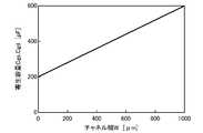
- a thin film transistor using an oxide semiconductor filmhas a property that the probability that the TFT is short-circuited increases as the channel width W increases (see FIG. 19). In other words, it has been found that the yield of TFT decreases as the channel width of the thin film transistor using the oxide semiconductor film increases.
- the present inventionhas been made in view of the above problems, and an object thereof is to provide a semiconductor element including an oxide semiconductor film, a thin film transistor substrate including the semiconductor element, and a display device with high yield.
- an invention according to claim 1is provided in a substrate, a gate electrode provided on the substrate, a gate insulating film provided so as to cover the gate electrode, and a gate insulating film upper layer. And an oxide semiconductor film having a channel portion formed at a position facing the gate electrode, and a source electrode and a drain electrode provided on the oxide semiconductor film so as to be spaced apart from each other with the channel portion interposed therebetween.
- a semiconductor elementwherein at least one of a source electrode and a drain electrode is arranged so as not to overlap with a gate electrode in plan view, and an adjacent region of the gate electrode and the source electrode and an adjacent gate electrode and the drain electrode In a region that does not overlap among the regions, a portion including the surface of the oxide semiconductor film is subjected to resistance reduction treatment.
- the parasitic capacitance C gs generated between the gate electrode and the source electrode or between the gate electrode and the drain electrodeis generated.
- the parasitic capacitance C gdcan be reduced.
- the resistance of the adjacent region of the gate electrode and the source electrode or the adjacent region of the gate electrode and the drain electrodeis reduced. Since it is processed, the parasitic capacitances C gs and C gd can be reduced without reducing the on-current of the thin film transistor.
- the parasitic capacitance generated between the gate electrode and the source electrode and / or the gate electrode and the drain electrodeis reduced, so that the channel width of the semiconductor element can be reduced. Then, by reducing the channel width of the semiconductor element including the oxide semiconductor film, the semiconductor element is less likely to be short-circuited, and as a result, a good yield can be obtained.
- the invention according to claim 2is the semiconductor element according to claim 1, wherein the region of the oxide semiconductor film subjected to the resistance reduction treatment has a sheet resistance of 10 ⁇ / ⁇ to 100 k ⁇ / ⁇ .
- the gate electrode and the source electrode and / or the gate electrode and the drain electrodedo not overlap, the adjacent regions of each electrode are subjected to the low resistance treatment, and the sheet resistance is 10 ⁇ / Since it is about ⁇ -100 k ⁇ / ⁇ , the on-state current of the semiconductor element does not decrease.
- the invention according to claim 3is the semiconductor element according to claim 1 or 2, wherein the channel portion has a channel width of 50 ⁇ m or less.
- the channel width of the semiconductor elementis 50 ⁇ m or less, the semiconductor element is hardly short-circuited. Therefore, a good yield can be obtained in the semiconductor element.
- the invention according to claim 4is the semiconductor device according to any one of claims 1 to 3, wherein the oxide semiconductor film is selected from the group consisting of indium (In), gallium (Ga), and zinc (Zn). It consists of a metal oxide containing at least one selected from the above.
- the oxide semiconductor layer made of these materialshas high mobility even if it is amorphous, so that the on-resistance of the semiconductor element can be increased.
- the invention according to claim 5is the semiconductor element according to claim 4, characterized in that the oxide semiconductor film is made of an In—Ga—Zn—O-based metal oxide.
- the semiconductor element according to any one of claims 1 to 5 of the present inventionhas a small channel width, a short circuit hardly occurs and a yield is good. Accordingly, when the semiconductor element according to any one of claims 1 to 5 is a thin film transistor as in the invention according to claim 6, the thin film transistor can be suitably used for a thin film transistor substrate provided on a substrate body. .
- the thin film transistor substrate according to claim 6includes a semiconductor element having a configuration in which the gate electrode and the source electrode and / or the gate electrode and the drain electrode do not overlap each other, and the channel width is reduced by reducing the parasitic capacitance between the respective electrodes. Since the semiconductor element can be made small, a short circuit of the semiconductor element hardly occurs and a good yield can be obtained. Accordingly, when the semiconductor element according to any one of claims 1 to 5 is provided in the final stage of the buffer circuit in the gate driver region and handles a large current as in the invention according to claim 7, a large channel is conventionally required.
- the present inventioncan also be particularly suitably used for a semiconductor element having a width.
- the thin film transistor substrate according to claim 6 or 7 of the present inventionincludes a semiconductor having a smaller channel width for reducing the parasitic capacitance between the gate electrode and the source electrode and / or the gate electrode and the drain electrode, a good yield can be obtained. It has excellent characteristics. Accordingly, the thin film transistor substrate of the present invention is the thin film transistor substrate according to claim 6, the counter substrate disposed to face the thin film transistor substrate, and the thin film transistor substrate as in the invention according to claim 8. And a display medium layer provided between the substrate and the display medium layer.
- the display device of the present inventioncan be suitably used for a display device in which the display medium layer is a liquid crystal layer, as in the ninth aspect of the invention.
- the parasitic capacitance C gs generated between the gate electrode and the source electrode or the parasitic capacitance generated between the gate electrode and the drain electrodesince the gate electrode and the source electrode, or the gate electrode and the drain electrode do not overlap, the parasitic capacitance C gs generated between the gate electrode and the source electrode or the parasitic capacitance generated between the gate electrode and the drain electrode.
- the capacity C gdcan be reduced.
- the parasitic capacitances C gs and C gdcan be reduced without reducing the on-current of the thin film transistor.
- the parasitic capacitance generated between the gate electrode and the source electrode and / or the gate electrode and the drain electrodeis reduced, so that the channel width of the semiconductor element can be reduced. Then, by reducing the channel width of the semiconductor element including the oxide semiconductor film, the semiconductor element is less likely to be short-circuited, and as a result, a good yield can be obtained.
- a good yieldcan be obtained in a semiconductor element including an oxide semiconductor, and a good yield can be obtained for a thin film transistor substrate and a display device including the semiconductor element.
- FIG. 2is a cross-sectional view taken along line II-II in FIG. It is the schematic which shows the electric circuit of the liquid crystal display device of this embodiment. It is a top view which expands and shows the principal part of the liquid crystal display device of this embodiment.
- FIG. 5is a cross-sectional view taken along line BB in FIG. 4 and is a cross-sectional view of the thin film transistor of the present embodiment.
- (A) And (b)is explanatory drawing which shows the manufacturing process of TFT, and respond
- FIG. 4(A) And (b) is explanatory drawing which shows the manufacturing process of TFT, and respond
- (A) And (b)is explanatory drawing which shows the manufacturing process of TFT, and respond
- (A) And (b)is a top view of the thin-film transistor for demonstrating channel length L.
- FIG.It is sectional drawing which shows the modification of the thin-film transistor of this embodiment. It is sectional drawing which shows the modification of the thin-film transistor provided in the pixel area. It is sectional drawing which shows the modification of the thin-film transistor of this embodiment. It is sectional drawing which shows the modification of the thin-film transistor of this embodiment. It is a top view which shows the modification of the thin-film transistor of this embodiment.
- 5is a graph showing the relationship between channel width W and parasitic capacitances C gs and C gd in a thin film transistor provided in a buffer circuit in a gate driver region. 5 is a graph showing a relationship between a channel width W and a TFT short-circuit rate in a thin film transistor provided in a buffer circuit in a gate driver region.
- FIG. 1is a plan view of a liquid crystal display device 1 having the TFT substrate 10 having a TFT S T according to the present embodiment
- FIG. 2is a sectional view taken along line II-II of Figure 1.
- FIG. 3is a schematic diagram of an electronic circuit in which the display region D and the gate driver region Tg of the TFT substrate 10 including the thin film transistor according to the present embodiment are enlarged.
- Figure 4is an enlarged plan view of the display region D and the gate driver region Tg of the TFT substrate 10 having a TFT S T according to the present embodiment, FIG. 5, the line B-B in FIG. 4, the present embodiment It is sectional drawing of the thin-film transistor of.
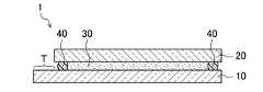
- the liquid crystal display device 1is arranged so that the TFT substrate 10 and the counter substrate 20 face each other, and both are bonded by a sealing material 40 provided on the outer peripheral edge of the substrate.
- a liquid crystal layer 30is provided as a display medium layer in a region surrounded by the sealing material 40.
- a display region D for displaying an imageis formed in an inner portion of the sealing material 40, and a terminal region T (gate driver region Tg and source driver is formed in a portion protruding from the counter substrate 20 of the TFT substrate 10. Region Ts) is formed.
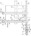
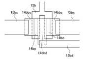
- the TFT substrate 10is provided in the display region D so as to extend in parallel to each other in a direction orthogonal to each of the scanning wirings 121 and a plurality of scanning wirings 121 provided so as to extend in parallel to each other. a plurality of signal lines 15l and, for each intersection of the scanning lines 12l and the signal lines 15l, that is, and a plurality of thin film transistors S P respectively provided for each pixel. A plurality of storage capacitor lines 12c are provided between the scanning lines 12l so as to extend in parallel with each other (not shown in FIG. 3, see FIG. 4). Further, TFT substrate 10, the gate driver region Tg, respective scanning lines 12l and the buffer circuit is configured for supplying a current to a thin film transistor S T to the final stage of the buffer circuit, with the configuration of this embodiment Is provided.
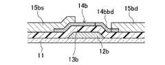
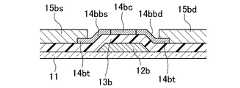
- the TFT substrate 10includes a first conductive film 12a-d, a first insulating film 13a-d, an oxide semiconductor film 14b, d, a second conductive film 15a-d, Passivation films 17a to 17d, planarization films 18a to 18d, and third conductive films 19a, c, and d are stacked.
- the first conductive film 12bis provided as the gate electrode, oxide layer of the gate electrode 12b via a gate insulating film 13b provided so as to cover the gate electrode 12b
- a semiconductor film 14bis provided. Note that a channel portion 14bc is formed in a position facing the gate electrode 12b in the oxide semiconductor film 14b.
- a source electrode 15bs and a drain electrode 15bdare provided over the oxide semiconductor film 14b by the second conductive film 15b so as to be separated from each other through the channel portion 14bc.
- a passivation film 17b and a planarizing film 18bare stacked so as to cover them.
- Each of the gate electrode 12b, the gate insulating film 13b, the source electrode 15bs, the drain electrode 15bd, the passivation film 17b, and the planarizing film 18bis made of a known material.
- the oxide semiconductor film 14bis made of, for example, an IGZO (In—Ga—Zn—O) -based metal oxide, and has a thickness of about 10 to 200 nm, for example. Even if an IGZO (In—Ga—Zn—O) -based metal oxide is amorphous, the mobility is high, and therefore, favorable characteristics for the thin film transistor ST such as high mobility and low off-state current can be obtained.
- the oxide semiconductor film 14bis formed using an IGZO (In—Ga—Zn—O) -based metal oxide; for example, a metal oxide containing any one of In, Ga, and Zn is used. What is necessary is just to be formed with the thing. These metal oxides have high mobility even amorphous, it is possible to form a large thin film transistor S T ON current.
- the drain electrode 15bd and the gate electrode 12bis formed so as not to overlap in plan view.
- the oxide semiconductor film 14bthe regions 14bbs adjacent to each other of the gate electrode 12b and the source electrode 15bs and the regions 14bbd adjacent to each other of the gate electrode 12b and the drain electrode 15bd are subjected to low resistance treatment, and the sheet resistance is reduced. It is about 10 ⁇ / ⁇ to 100k ⁇ / ⁇ .
- the low resistance regions 14bbs and 14bbdare formed to have a width of about 5 to 300 ⁇ m, for example.
- the low resistance portioncan have a thickness of about 2 to 20 nm, for example, and can have a thickness other than that.
- the channel portion 14bcis formed, for example, in a rectangular shape, and has a channel width W of about 5 to 300 ⁇ m and a channel length L of about 2 to 20 ⁇ m (see FIG. 11B).
- the thin film transistor S T, the gate electrode 12b and the source electrode 15bs, or the gate electrode 12b and the drain electrode 15bddo not overlap, the parasitic capacitance C gs, a gate electrode 12b generated between the gate electrode 12b and the source electrode 15bs and The parasitic capacitance C gd generated between the drain electrodes 15bd can be reduced.
- the gate electrode 12b and the source electrode 15bs, or the gate electrode 12b and the drain electrode 15bddo not overlap with each other, the region 14bbs adjacent to each other of the gate electrode 12b and the source electrode 15bs in the oxide semiconductor film 14b, or since mutually adjacent regions 14bbd the gate electrode 12b and the drain electrode 15bd is processed low resistance, the parasitic capacitance C gs without reducing the oN-current of the thin film transistor S T, it is possible to reduce the C gd.
- the same structure as the known TFT substrateFirst conductive films 12a, c, d, first insulating films 13a, c, d, oxide semiconductor film 14d, second conductive films 15a, c, d, passivation films 17a, c, d, planarization
- the films 18a, c, d and the third conductive films 19a, c, dare stacked (see FIG. 8B).
- the counter substrate 20is provided with a color filter layer including a light shielding layer and a colored layer on the substrate, a common electrode is provided so as to cover the color filter layer, and an alignment film is provided so as to cover the common electrode. Yes.
- the liquid crystal layer 30is made of, for example, a nematic liquid crystal material having electro-optical characteristics.
- the liquid crystal display device 1in each pixel, it is sent to the gate electrode 12b a gate signal from the gate driver via the scanning lines 12l, when the thin film transistor S P output display region D is turned on, the thin film transistor in S P, is sent to the source electrode 15ds through the source signal from the source driver signal line 15l, via the oxide semiconductor film 14d and the drain electrode 15Dd, predetermined charge is written in the pixel electrode 19d.
- a potential differenceis generated between each pixel electrode 19d of the TFT substrate 10 and the common electrode of the counter substrate 20, and the liquid crystal layer 30, that is, the liquid crystal capacitance of each pixel, and the auxiliary capacitance connected in parallel to the liquid crystal capacitance.
- a predetermined voltageis applied to the element Cs.
- an imageis displayed by adjusting the light transmittance of the liquid crystal layer 30 by changing the alignment state of the liquid crystal layer 30 according to the magnitude of the voltage applied to the liquid crystal layer 30 in each pixel. .
- TFT substrate manufacturing methoda method for manufacturing the TFT substrate 10 according to the present embodiment will be described with reference to FIGS.
- a first conductive filmis formed on a substrate 11 by laminating, for example, a Ti film having a thickness of about 30 nm, an Al film having a thickness of about 200 nm, and a Ti film having a thickness of about 100 nm, and the gate source contact portion GS.
- a SiN film having a thickness of about 325 nm and a SiO 2 film having a thickness of about 50 nmare stacked on the patterned first conductive films 12a to 12d to form first insulating films 13a to 13a. d is deposited.
- an oxide semiconductor film having a thickness of about 40 nm, as shown in FIG. 6 (b), the thin film transistor S T of the gate driver region Tg, so as to correspond to each of the thin film transistor S P output display region D Patterningis performed.
- the sheet resistance of the oxide semiconductor films 14b and d formed hereis, for example, about 1 ⁇ 10 12 to 1 ⁇ 10 17 ⁇ / ⁇ .
- patterningmay be performed so that the oxide semiconductor film also covers the storage capacitor element Cs.
- a Ti film having a thickness of about 30 nm, an Al film having a thickness of about 200 nm, and a Ti film having a thickness of about 100 nmare stacked to form a second conductive film, and patterning is performed.
- the end portion of the second conductive film 15ais located above the first conductive film 12a with the first insulating film 13a interposed therebetween.
- Pattern.In the thin film transistor S T of the gate driver region Tg, the upper layer of the first conductive film 12b so as not to overlap the source electrode 15bs and the drain electrode 15bd, a source electrode 15bs and the drain electrode 15bd.
- the second conductive film 15cis provided so as to cover the upper part thereof. Then, in the thin film transistor S P output display area D, so that the source electrode 15ds and the drain electrode 15dd oxide semiconductor film 14d of the upper layer of the first conductive film 12d is leaving the portion to be a channel portion 14dc are respectively formed The second conductive film 15d is patterned.
- the gate electrode 12b and the source electrode while the gate electrode 12b and the drain electrode 15bd are provided so as not to overlap in a plan view 15bsmay be provided so as to partially overlap. Even in this case, since the parasitic capacitance C gd between the gate electrode 12b and the drain electrode 15bd is reduced, the channel width W can be reduced accordingly. Conversely, the gate electrode 12b and the source electrode 15bs may be provided so as not to overlap in plan view, while the gate electrode 12b and the drain electrode 15bd may be provided so as to partially overlap each other.
- a resist filmis applied to a thickness of 1 to 2 ⁇ m, followed by exposure and development to form resists 16a to 16d. Note that exposure is performed from the substrate side (opposite side of the resist) so that the resists 16a to 16d are formed only on the first conductive film 12 and the second conductive film 15. In this case, in the forming portion of the thin film transistor S T of the gate driver region Tg, to adjust the exposure time to form a resist 16b inside the to correspond to the channel portion 14bc.
- the resist 16b defining the channel portion 14bchas a width smaller than the width of the gate electrode 12b. Therefore, when the channel length L of the channel portion 114c is defined by patterning using a mask as shown in FIGS. 11A and 12A (that is, the mask size M matches the channel length L). 11 (b) and FIG. 12 (b), the channel length L of the channel portion 14bc is formed by forming the width of the gate electrode so as to coincide with the mask size M, as shown in FIGS. Can be made smaller than the size M of the mask. Therefore, on-current of the thin film transistor S T increases, thereby enabling faster driving.
- the low resistance of the regions not covered with the resists 16b and d of the oxide semiconductor films 14b and dby performing an annealing process or a hydrogen plasma process in a hydrogen atmosphere.
- the region not covered with the resist 16b and the second conductive film 15b of the oxide semiconductor film 14bis made of sheet resistance for example, 10 ⁇ / ⁇ ⁇ 100k ⁇ / ⁇ .
- the resists 16a to 16dare removed.
- an SiO 2 film having a thickness of, for example, about 265 nmis formed as the passivation films 17a to 17d on the entire surface of the substrate 11, and a photosensitive resin is used as the planarizing films 18a to 18d, for example.
- a filmis formed.
- a contact hole Cais formed on both surfaces of the first conductive film 12a and the second conductive film 15a.
- a contact hole Cc that reaches the second conductive film 15c from the planarizing film 18cis formed.
- an ITO film having a thickness of, for example, about 100 nmis formed as the third conductive film 19a, c, d, so as to cover the surface of the contact hole Ca in the gate source contact portion GS, and in the display region D. Patterning is performed so as to form the pixel electrode 19d (19c) including the thin film transistor SP and the auxiliary capacitance element Cs.
- an alignment filmis formed so as to cover the display region D, and the TFT substrate 10 is completed.
- the TFT substrate 10is bonded to, for example, a counter substrate 20 that is separately produced by a known method through a sealing material 40, and a liquid crystal layer 30 is provided between both substrates, thereby forming the liquid crystal display device 1. Can do.
- an oxide semiconductor film 14b, an upper layer of the 14d and the second conductive film 15b, the lower layer of the 15d, the channel portion 14bc, respectively so as to cover the 14dc second insulating film 50b, 50dMay be formed.
- the channel portion 14bc of the oxide semiconductor film 14b oxide semiconductor film 14bAs shown in FIG. 13, in the case of providing the second insulating film 50b so as to cover the channel portion 14bc of the thin film transistor S T of the gate driver region Tg is the channel portion 14bc of the oxide semiconductor film 14b oxide semiconductor film 14b formed Since the second insulating film 50b can be covered immediately after the film, the channel portion 14bc is not easily subjected to stress such as electrical and temperature due to external factors, and the operating characteristics of the TFT are improved.
- the resistance reduction treatment of the oxide semiconductor film 14bmay be performed after the oxide semiconductor film patterning.
- the oxide semiconductor film 14bhas a low resistance when the second conductive films 15bs and 15bd are patterned.
- the low resistance region 14bu on the surfaceis etched and only the lower portion 14bl of the lower resistance region that is not subjected to the low resistance treatment remains. Therefore, when the resistance reduction process of the oxide semiconductor film 14b is performed before the second conductive films 15bs and 15bd are provided, it is necessary to control the thickness, the etching depth, and the like of the resistance reduction process.
- a plurality of channel portions 14bcmay be provided over one oxide semiconductor film 14b.
- two source electrodes 15bsare provided so as to sandwich two channel portions 14bc positioned opposite to each other, and a drain electrode 15bd is provided at an end of both channel portions 14bc. It can be a layout.
- a process of reducing the resistance of the region 14bbs between the source electrode 15bs and the gate electrode 12b and the region 14bbd between the drain electrode 15bd and the gate electrode 12bis performed.
- a thin-film transistor S T of the present inventionin the final stage of the gate driver region Tg, it may form a thin film transistor S T of the configuration of the present invention other than the final stage of the gate driver region Tg, it may form a thin film transistor S T of the configuration of the present invention so as to correspond to each pixel in the display area D.
- the gate electrode 12b and the source electrode 15bs or the gate electrode 12b and the drain electrode 15bddo not overlap, the parasitic capacitance C gs generated between the gate electrode 12b and the source electrode 15bs, The parasitic capacitance C gd generated between the gate electrode 12b and the drain electrode 15bd can be reduced.
- the gate electrode 12b and the source electrode 15bs, or the gate electrode 12b and the drain electrode 15bddo not overlap with each other, the region 14bbs adjacent to each other of the gate electrode 12b and the source electrode 15bs in the oxide semiconductor film 14b, or Since the region 14bbd adjacent to each other of the gate electrode 12b and the drain electrode 15bd is subjected to a resistance reduction process, the parasitic capacitances C gs and C gd can be reduced without reducing the on-current of the thin film transistor.
- the parasitic capacitance C gs generated between the gate electrode 12b and the source electrode 15bs, and / or the gate electrode 12b and the drain electrode 15bd, by C gdis reduced, reducing the channel width W of the thin film transistor S T Can do. Then, by reducing the channel width W of the thin film transistor S T having the oxide semiconductor film 14b, short of the thin film transistor S T is less likely to occur, as a result, it is possible to obtain a good yield.
- the present inventionis useful for a semiconductor element including an oxide semiconductor film, a thin film transistor substrate including the semiconductor element, and a display device.
- SYMBOLS 1Liquid crystal display device Tg Gate driver area
Landscapes
- Physics & Mathematics (AREA)
- Nonlinear Science (AREA)
- Engineering & Computer Science (AREA)
- Microelectronics & Electronic Packaging (AREA)
- Mathematical Physics (AREA)
- Chemical & Material Sciences (AREA)
- Crystallography & Structural Chemistry (AREA)
- General Physics & Mathematics (AREA)
- Optics & Photonics (AREA)
- Thin Film Transistor (AREA)
- Liquid Crystal (AREA)
Abstract
Description
Translated fromJapanese本発明は、酸化物半導体膜を備えた半導体素子に関する。また、本発明は、その半導体素子を備えた薄膜トランジスタ基板や表示装置に関する。The present invention relates to a semiconductor element including an oxide semiconductor film. The present invention also relates to a thin film transistor substrate and a display device including the semiconductor element.
アクティブマトリクス基板としては、画像の最小単位である各画素毎に、スイッチング素子として薄膜トランジスタ(Thin Film Transistor、以下、「TFT」とも称する)が設けられた薄膜トランジスタ基板(以下、「TFT基板」とも称する)が広く用いられている。As an active matrix substrate, a thin film transistor substrate (hereinafter also referred to as “TFT substrate”) in which a thin film transistor (Thin Film Transistor, hereinafter also referred to as “TFT”) is provided as a switching element for each pixel which is the minimum unit of an image. Is widely used.
一般的な構成のTFTは、例えば、絶縁基板上に設けられたゲート電極と、ゲート電極を覆うように設けられたゲート絶縁膜と、ゲート絶縁膜上にゲート電極に重なるように島状に設けられた半導体層と、半導体層上に互いに対峙するように設けられたソース電極及びドレイン電極とを備えている。半導体層としては、一般に、アモルファスシリコン半導体膜で構成されたものが用いられる(例えば、特許文献1参照)。A TFT having a general configuration is provided in an island shape, for example, on a gate electrode provided on an insulating substrate, a gate insulating film provided so as to cover the gate electrode, and on the gate insulating film so as to overlap the gate electrode. And a source electrode and a drain electrode provided on the semiconductor layer so as to face each other. As the semiconductor layer, one composed of an amorphous silicon semiconductor film is generally used (see, for example, Patent Document 1).
そして、この平坦化膜上に画素電極が形成されてTFT基板が製造されるとともに、TFT基板に対向するように対向基板を設け、TFT基板及び対向基板の間に液晶層を設けることにより、液晶表示装置が製造される。Then, a pixel electrode is formed on the planarizing film to manufacture a TFT substrate, and a counter substrate is provided so as to face the TFT substrate, and a liquid crystal layer is provided between the TFT substrate and the counter substrate. A display device is manufactured.
近年、TFT基板では、画像の最小単位である各画素のTFTとして、アモルファスシリコン(a-Si)からなる半導体層に代わって、酸化物半導体からなる半導体膜(以下、「酸化物半導体膜」とも称する)を用いたTFTが提案されている。酸化物半導体膜は、a-Si半導体膜と比較して、電子移動度が大きい、低温プロセスが可能、電気ストレスによるTFTの特性変動が小さい、等の点で優れている。特に、酸化物半導体膜を用いたTFTは、電子移動度が大きく、電気ストレスによるTFTの特性変動が小さいために、ドライバ回路面積を小さく形成することができる点で注目されている。In recent years, in TFT substrates, as a TFT of each pixel, which is the minimum unit of an image, a semiconductor film made of an oxide semiconductor (hereinafter referred to as an “oxide semiconductor film”) is used instead of a semiconductor layer made of amorphous silicon (a-Si). TFTs using the above have been proposed. An oxide semiconductor film is superior to an a-Si semiconductor film in that it has a high electron mobility, a low temperature process is possible, and a TFT characteristic variation due to electrical stress is small. In particular, a TFT using an oxide semiconductor film is attracting attention because it has a high electron mobility and a small characteristic variation of the TFT due to an electrical stress, so that a driver circuit area can be reduced.
また、近年、モバイル機器に搭載する表示装置の小型化の要求が大きく、表示装置上にドライバ回路を同時形成することにより後付けのドライバチップが不要なモノリシック表示装置の研究開発が盛んに行われている。モノリシック表示装置に用いるTFTとしては、ドライバ回路面積を小さく形成可能である点で、酸化物半導体TFTが好適であり、酸化物半導体TFTのモノリシック表示装置への応用が期待されている。In recent years, there has been a great demand for miniaturization of display devices mounted on mobile devices, and research and development of monolithic display devices that do not require a retrofit driver chip by simultaneously forming a driver circuit on the display device have been actively conducted. Yes. As a TFT used in a monolithic display device, an oxide semiconductor TFT is suitable because it can be formed with a small driver circuit area, and application of the oxide semiconductor TFT to a monolithic display device is expected.
一般に、表示装置のTFTとしては、製造コストが低いボトムゲート構造が採用されている。このボトムゲート構造TFTは、ゲート電極とソース電極、及びゲート電極とドレイン電極のそれぞれの一部が重なり合うように設けられている。このような構造のTFTでドライバ回路を構成すると、そのオーバーラップした部分で寄生容量が発生するので、大きな寄生容量をカバーするためにも、薄膜トランジスタのチャネル幅を大きくする必要がある(図18参照)。特に、ゲートドライバのバッファ回路のうち最終段を構成する薄膜トランジスタでは、画素領域の薄膜トランジスタよりも大きな電流を扱うので、TFTのチャネル幅を非常に大きくしなければならない。例えば、ゲートドライバのバッファ回路の最終段を構成する薄膜トランジスタとしては、現状ではチャネル幅が800μm程度のものが作製されている。Generally, a bottom gate structure with a low manufacturing cost is adopted as a TFT of a display device. This bottom gate structure TFT is provided so that a part of each of a gate electrode and a source electrode, and a gate electrode and a drain electrode may overlap. When a driver circuit is configured with TFTs having such a structure, parasitic capacitance is generated in the overlapped portion. Therefore, in order to cover a large parasitic capacitance, it is necessary to increase the channel width of the thin film transistor (see FIG. 18). ). In particular, since the thin film transistor constituting the final stage of the buffer circuit of the gate driver handles a larger current than the thin film transistor in the pixel region, the channel width of the TFT must be very large. For example, as a thin film transistor constituting the final stage of the gate driver buffer circuit, a thin film transistor having a channel width of about 800 μm is currently manufactured.
ところで、本発明者は、酸化物半導体膜を用いた薄膜トランジスタは、チャネル幅Wが大きくなるにつれてTFTがショートする確率が大きくなるという性質を有することを見いだした(図19参照)。つまり、酸化物半導体膜を用いた薄膜トランジスタのチャネル幅が大きくなるとTFTの歩留まりが低下することが分かった。By the way, the present inventor has found that a thin film transistor using an oxide semiconductor film has a property that the probability that the TFT is short-circuited increases as the channel width W increases (see FIG. 19). In other words, it has been found that the yield of TFT decreases as the channel width of the thin film transistor using the oxide semiconductor film increases.
本発明は、上述の問題に鑑みてなされたものであり、酸化物半導体膜を備えた半導体素子、それを備えた薄膜トランジスタ基板、及び表示装置を歩留まりよく提供することを目的とする。The present invention has been made in view of the above problems, and an object thereof is to provide a semiconductor element including an oxide semiconductor film, a thin film transistor substrate including the semiconductor element, and a display device with high yield.
上記目的を達成するために、請求項1に記載の発明は、基板と、基板上に設けられたゲート電極と、ゲート電極上を覆って設けられたゲート絶縁膜と、ゲート絶縁膜上層に設けられ、ゲート電極に対向する位置にチャネル部が形成された酸化物半導体膜と、酸化物半導体膜上に、チャネル部を介して互いに離間して設けられたソース電極及びドレイン電極と、を備えた半導体素子であって、ソース電極及びドレイン電極のうち少なくとも一方は、ゲート電極と平面視で重ならないように配置され、ゲート電極とソース電極の互いに隣接する領域及びゲート電極とドレイン電極の互いに隣接する領域のうち重なり合わない領域において、酸化物半導体膜の表面を含む部分が低抵抗化処理されていることを特徴とする。In order to achieve the above object, an invention according to
上記の構成によれば、ゲート電極とソース電極、或いはゲート電極とドレイン電極がオーバーラップしていないので、ゲート電極・ソース電極間に発生する寄生容量Cgsやゲート電極・ドレイン電極間に発生する寄生容量Cgdを低減することができる。また、ゲート電極とソース電極、或いはゲート電極とドレイン電極がオーバーラップしていなくても、ゲート電極とソース電極の互いに隣接する領域、或いは、ゲート電極とドレイン電極の互いに隣接する領域が低抵抗化処理されているので、薄膜トランジスタのオン電流を低下させることなく寄生容量Cgs、Cgdを低減することができる。従って、ゲート電極とソース電極、及び/またはゲート電極とドレイン電極の間に発生する寄生容量が低減されることにより、半導体素子のチャネル幅を小さくすることができる。そして、酸化物半導体膜を備えた半導体素子のチャネル幅を小さくすることにより、半導体素子のショートが起こりにくくなり、結果として、良好な歩留まりが得られる。According to the above configuration, since the gate electrode and the source electrode or the gate electrode and the drain electrode do not overlap with each other, the parasitic capacitance Cgs generated between the gate electrode and the source electrode or between the gate electrode and the drain electrode is generated. The parasitic capacitance Cgd can be reduced. In addition, even when the gate electrode and the source electrode or the gate electrode and the drain electrode do not overlap, the resistance of the adjacent region of the gate electrode and the source electrode or the adjacent region of the gate electrode and the drain electrode is reduced. Since it is processed, the parasitic capacitances Cgs and Cgd can be reduced without reducing the on-current of the thin film transistor. Accordingly, the parasitic capacitance generated between the gate electrode and the source electrode and / or the gate electrode and the drain electrode is reduced, so that the channel width of the semiconductor element can be reduced. Then, by reducing the channel width of the semiconductor element including the oxide semiconductor film, the semiconductor element is less likely to be short-circuited, and as a result, a good yield can be obtained.
請求項2に記載の発明は、請求項1に記載された半導体素子において、酸化物半導体膜のうち低抵抗化処理された領域は、シート抵抗が10Ω/□~100kΩ/□であることを特徴とする。The invention according to claim 2 is the semiconductor element according to
上記の構成によれば、ゲート電極とソース電極、及び/またはゲート電極とドレイン電極がオーバーラップしていなくても、それぞれの電極の互いに隣接する領域が低抵抗化処理されてシート抵抗が10Ω/□~100kΩ/□程度となっているので、半導体素子のオン電流が低下することがない。According to the above configuration, even if the gate electrode and the source electrode and / or the gate electrode and the drain electrode do not overlap, the adjacent regions of each electrode are subjected to the low resistance treatment, and the sheet resistance is 10Ω / Since it is about □ -100 kΩ / □, the on-state current of the semiconductor element does not decrease.
請求項3に記載の発明は、請求項1または2に記載された半導体素子において、チャネル部は、チャネル幅が50μm以下であることを特徴とする。The invention according to claim 3 is the semiconductor element according to
上記の構成によれば、半導体素子のチャネル幅が50μm以下であるので、半導体素子のショートが起こりにくい。従って、半導体素子において良好な歩留まりが得られる。According to the above configuration, since the channel width of the semiconductor element is 50 μm or less, the semiconductor element is hardly short-circuited. Therefore, a good yield can be obtained in the semiconductor element.
請求項4に記載の発明は、請求項1~3のいずれかに記載された半導体素子において、酸化物半導体膜が、インジウム(In)、ガリウム(Ga)及び亜鉛(Zn)からなる群より選ばれる少なくとも1種を含む金属酸化物からなることを特徴とする。The invention according to
上記の構成によれば、これらの材料からなる酸化物半導体層は、アモルファスであっても移動度が高いため、半導体素子のオン抵抗を大きくすることができる。According to the above structure, the oxide semiconductor layer made of these materials has high mobility even if it is amorphous, so that the on-resistance of the semiconductor element can be increased.
請求項5に記載の発明は、請求項4に記載の半導体素子において、酸化物半導体膜が、In-Ga-Zn-O系の金属酸化物からなることを特徴とする。The invention according to
上記の構成によれば、TFTにおいて、高移動度、低オフ電流といった良好な特性を得ることができる。According to the above configuration, good characteristics such as high mobility and low off-state current can be obtained in the TFT.
本発明の請求項1~5のいずれかに記載の半導体素子は、チャネル幅が小さいので、ショートが起こりにくく歩留まりがよい。従って、請求項6に記載の発明のように、請求項1~5のいずれかに記載された半導体素子が薄膜トランジスタである場合に、その薄膜トランジスタを基板本体上に備えた薄膜トランジスタ基板に好適に使用できる。Since the semiconductor element according to any one of
請求項6に記載の薄膜トランジスタ基板は、ゲート電極とソース電極、及び/またはゲート電極とドレイン電極がオーバーラップしない構成の半導体素子を備え、それぞれの電極間の寄生容量を低減することによりチャネル幅を小さくすることができるので、半導体素子のショートが起こりにくく良好な歩留まりが得られる。従って、請求項7に記載の発明のように、請求項1~5のいずれかに記載の半導体素子がゲートドライバ領域のバッファ回路の最終段に設けられて大きな電流を取り扱う場合に従来では大きなチャネル幅に構成されていた半導体素子にも、特に好適に使用できる。The thin film transistor substrate according to claim 6 includes a semiconductor element having a configuration in which the gate electrode and the source electrode and / or the gate electrode and the drain electrode do not overlap each other, and the channel width is reduced by reducing the parasitic capacitance between the respective electrodes. Since the semiconductor element can be made small, a short circuit of the semiconductor element hardly occurs and a good yield can be obtained. Accordingly, when the semiconductor element according to any one of
本発明の請求項6または7に記載の薄膜トランジスタ基板は、ゲート電極とソース電極、及び/またはゲート電極とドレイン電極間の寄生容量の低減により小さいチャネル幅の半導体を備えるので良好な歩留まりが得られるという優れた特性を備えている。従って、本発明の薄膜トランジスタ基板は、請求項8に記載の発明のように、請求項6または7に記載された薄膜トランジスタ基板と、薄膜トランジスタ基板に対向して配置された対向基板と、薄膜トランジスタ基板と対向基板との間に設けられた表示媒体層と、を備える表示装置に好適に使用できる。Since the thin film transistor substrate according to claim 6 or 7 of the present invention includes a semiconductor having a smaller channel width for reducing the parasitic capacitance between the gate electrode and the source electrode and / or the gate electrode and the drain electrode, a good yield can be obtained. It has excellent characteristics. Accordingly, the thin film transistor substrate of the present invention is the thin film transistor substrate according to claim 6, the counter substrate disposed to face the thin film transistor substrate, and the thin film transistor substrate as in the invention according to claim 8. And a display medium layer provided between the substrate and the display medium layer.
本発明の表示装置は、請求項9に記載の発明のように、表示媒体層が液晶層である表示装置に好適に使用できる。The display device of the present invention can be suitably used for a display device in which the display medium layer is a liquid crystal layer, as in the ninth aspect of the invention.
本発明によれば、ゲート電極とソース電極、或いはゲート電極とドレイン電極がオーバーラップしていないので、ゲート電極・ソース電極間に発生する寄生容量Cgsやゲート電極・ドレイン電極間に発生する寄生容量Cgdを低減することができる。また、ゲート電極とソース電極、或いはゲート電極とドレイン電極がオーバーラップしていなくても、ゲート電極とソース電極の互いに隣接する領域、或いは、ゲート電極とドレイン電極の互いに隣接する領域が低抵抗化処理されているので、薄膜トランジスタのオン電流を低下させることなく寄生容量Cgs、Cgdを低減することができる。従って、ゲート電極とソース電極、及び/またはゲート電極とドレイン電極の間に発生する寄生容量が低減されることにより、半導体素子のチャネル幅を小さくすることができる。そして、酸化物半導体膜を備えた半導体素子のチャネル幅を小さくすることにより、半導体素子のショートが起こりにくくなり、結果として、良好な歩留まりが得られる。According to the present invention, since the gate electrode and the source electrode, or the gate electrode and the drain electrode do not overlap, the parasitic capacitance Cgs generated between the gate electrode and the source electrode or the parasitic capacitance generated between the gate electrode and the drain electrode. The capacity Cgd can be reduced. In addition, even when the gate electrode and the source electrode or the gate electrode and the drain electrode do not overlap, the resistance of the adjacent region of the gate electrode and the source electrode or the adjacent region of the gate electrode and the drain electrode is reduced. Since it is processed, the parasitic capacitances Cgs and Cgd can be reduced without reducing the on-current of the thin film transistor. Accordingly, the parasitic capacitance generated between the gate electrode and the source electrode and / or the gate electrode and the drain electrode is reduced, so that the channel width of the semiconductor element can be reduced. Then, by reducing the channel width of the semiconductor element including the oxide semiconductor film, the semiconductor element is less likely to be short-circuited, and as a result, a good yield can be obtained.
また、上述のように、酸化物半導体を備えた半導体素子において良好な歩留まりが得られるのに伴って、当該半導体素子を備えた薄膜トランジスタ基板や表示装置についても良好な歩留まりが得られる。In addition, as described above, a good yield can be obtained in a semiconductor element including an oxide semiconductor, and a good yield can be obtained for a thin film transistor substrate and a display device including the semiconductor element.
以下、本発明の実施形態について、図面を参照しながら詳細に説明する。なお、本発明は以下の実施形態に限定されるものではない。Hereinafter, embodiments of the present invention will be described in detail with reference to the drawings. In addition, this invention is not limited to the following embodiment.
(液晶表示装置の構成)
図1は、本実施形態に係る薄膜トランジスタSTを備えるTFT基板10を有する液晶表示装置1の平面図であり、図2は、図1のII-II線における断面図である。また、図3は、本実施形態に係る薄膜トランジスタを備えるTFT基板10の表示領域D及びゲートドライバ領域Tgを拡大した電子回路の概略図である。図4は、本実施形態に係る薄膜トランジスタSTを備えるTFT基板10の表示領域D及びゲートドライバ領域Tgを拡大した平面図であり、図5は、図4のB-B線における、本実施形態の薄膜トランジスタの断面図である。(Configuration of liquid crystal display device)
Figure 1 is a plan view of a liquid
液晶表示装置1は、TFT基板10と対向基板20とが互いに対向するように配置され、基板外周縁部に設けられたシール材40により両者が接着されている。そして、シール材40に囲まれた領域に、表示媒体層として液晶層30が設けられている。The liquid
また、液晶表示装置1では、シール材40の内側の部分に画像表示を行う表示領域Dが形成され、TFT基板10の対向基板20から突出する部分に端子領域T(ゲートドライバ領域Tg及びソースドライバ領域Ts)が形成されている。Further, in the liquid
TFT基板10は、図3に示すように、表示領域Dにおいて、互いに並行に延びるように設けられた複数の走査配線12lと、各走査配線12lと直交する方向に互いに並行に延びるように設けられた複数の信号配線15lと、各走査配線12l及び各信号配線15lの交差部分毎、すなわち、各画素毎にそれぞれ設けられた複数の薄膜トランジスタSPと、を備えている。なお、各走査配線12lの間には、互いに並行に延びるように複数の補助容量配線12cが設けられている(図3には不図示、図4参照)。また、TFT基板10は、ゲートドライバ領域Tgにおいて、各走査配線12lに電流を流すためのバッファ回路が構成されており、そのバッファ回路の最終段に、本実施形態の構成を備えた薄膜トランジスタSTが設けられている。As shown in FIG. 3, the
また、積層構造の点からは、TFT基板10は、基板11上に第1導電膜12a~d、第1絶縁膜13a~d、酸化物半導体膜14b,d、第2導電膜15a~d、パッシベーション膜17a~d、平坦化膜18a~d、及び第3導電膜19a,c,dが積層された構成を有している。From the viewpoint of the laminated structure, the
薄膜トランジスタSTにおいては、図5に示すように、第1導電膜12bがゲート電極として設けられ、ゲート電極12bを覆うように設けられたゲート絶縁膜13bを介してゲート電極12bの上層に酸化物半導体膜14bが設けられている。なお、酸化物半導体膜14bのうちゲート電極12bに対向する位置にはチャネル部14bcが形成されている。また、酸化物半導体膜14bの上層には、チャネル部14bcを介して互いに離間して、第2導電膜15bによりソース電極15bsとドレイン電極15bdとが設けられている。そして、これらを覆うようにパッシベーション膜17b及び平坦化膜18bが積層されている。In the thin film transistor ST, as shown in FIG. 5, the first
ゲート電極12b、ゲート絶縁膜13b、ソース電極15bs、ドレイン電極15bd、パッシベーション膜17b、平坦化膜18bのそれぞれは、公知の材料で構成されている。Each of the
酸化物半導体膜14bは、例えば、IGZO(In-Ga-Zn-O)系の金属酸化物により形成されており、例えば厚さが10~200nm程度である。IGZO(In-Ga-Zn-O)系の金属酸化物はアモルファスであっても移動度が高いので、高移動度、低オフ電流といった薄膜トランジスタSTにとって良好な特性が得られる。なお、ここでは酸化物半導体膜14bがIGZO(In-Ga-Zn-O)系の金属酸化物で形成されているとしたが、例えばIn、Ga、及びZnのいずれか1種を含む金属酸化物で形成されていればよい。これらの金属酸化物はアモルファスであっても移動度が高いため、オン電流の大きい薄膜トランジスタSTを形成することができる。The
薄膜トランジスタSTは、ソース電極15bsとゲート電極12bが平面視で重ならないように、また、ドレイン電極15bdとゲート電極12bが平面視で重ならないように形成されている。そして、酸化物半導体膜14bのうちゲート電極12bとソース電極15bsの互いに隣接する領域14bbs、及び、ゲート電極12bとドレイン電極15bdの互いに隣接する領域14bbdが低抵抗化処理されており、シート抵抗が10Ω/□~100kΩ/□程度になっている。この低抵抗化された領域14bbs,14bbdは、幅が例えば5~300μm程度に形成されている。なお、ここでの酸化物半導体膜14bの低抵抗化処理においては、酸化物半導体膜14bの表面を含む部分が少なくとも低抵抗化されていればよい。なお、ここでの酸化物半導体膜14bの低抵抗化処理においては、酸化物半導体膜14bの表面を含む部分が少なくとも低抵抗化されていればよい。低抵抗化された部分は、一例として、例えば2~20nm程度の厚さとすることができ、それ以外の厚さとすることも可能である。TFT ST, as the source electrode 15bs and the
酸化物半導体膜14bのうち、低抵抗化された領域14bbs,14bbdで挟まれる領域は、チャネル部14bcを構成している。チャネル部14bcは、例えば矩形に形成され、チャネル幅Wが5~300μm程度及びチャネル長Lが2~20μm程度である(図11(b)参照)。Of the
この薄膜トランジスタSTは、ゲート電極12bとソース電極15bs、或いはゲート電極12bとドレイン電極15bdがオーバーラップしていないので、ゲート電極12b及びソース電極15bs間に発生する寄生容量Cgsやゲート電極12b及びドレイン電極15bd間に発生する寄生容量Cgdを低減することができる。また、ゲート電極12bとソース電極15bs、或いはゲート電極12bとドレイン電極15bdがオーバーラップしていなくても、酸化物半導体膜14bのうちゲート電極12bとソース電極15bsの互いに隣接する領域14bbs、或いは、ゲート電極12bとドレイン電極15bdの互いに隣接する領域14bbdが低抵抗化処理されているので、薄膜トランジスタSTのオン電流を低下させることなく寄生容量Cgs、Cgdを低減することができる。The thin film transistorS T, the
なお、端子領域Tに形成された薄膜トランジスタST以外(例えば、補助容量素子Cs、表示領域Dに形成された薄膜トランジスタSP、ゲートソースコンタクト部GS等)は、公知のTFT基板と同様の構造となるように、第1導電膜12a,c,d、第1絶縁膜13a,c,d、酸化物半導体膜14d、第2導電膜15a,c,d、パッシベーション膜17a,c,d、平坦化膜18a,c,d、及び第3導電膜19a,c,dが積層されている(図8(b)参照)。Incidentally, other than the thin film transistor ST formed in the terminal region T (e.g., the auxiliary capacitor element Cs, a thin film transistor SP formed in the display regionD, the gate source contact portion GS, etc.), the same structure as the known TFT substrate First
対向基板20は、基板上に遮光層及び着色層を備えたカラーフィルタ層が設けられ、カラーフィルタ層を覆うように共通電極が設けられ、さらに、共通電極を覆うように配向膜が設けられている。The
液晶層30は、例えば、電気光学特性を有するネマチックの液晶材料などにより構成されている。The
上記構成の液晶表示装置1では、各画素において、ゲートドライバからゲート信号が走査配線12lを介してゲート電極12bに送られて、表示領域Dの薄膜トランジスタSPがオン状態になったときに、薄膜トランジスタSPにおいて、ソースドライバからソース信号が信号配線15lを介してソース電極15dsに送られて、酸化物半導体膜14d及びドレイン電極15ddを介して、画素電極19dに所定の電荷が書き込まれる。この際、TFT基板10の各画素電極19dと対向基板20の共通電極との間において電位差が生じ、液晶層30、すなわち、各画素の液晶容量、及びその液晶容量に並列に接続された補助容量素子Csに所定の電圧が印加される。そして、液晶表示装置1では、各画素において、液晶層30に印加する電圧の大きさによって液晶層30の配向状態を変えることにより、液晶層30の光透過率を調整して画像が表示される。In the liquid
(TFT基板の製造方法)
以下、本実施形態に係るTFT基板10の製造方法について図6~8を用いて説明する。(TFT substrate manufacturing method)
Hereinafter, a method for manufacturing the
まず、基板11上に、例えば厚さ30nm程度のTi膜、厚さ200nm程度のAl膜、及び厚さ100nm程度のTi膜を積層して第1導電膜を成膜し、ゲートソースコンタクト部GS、ゲートドライバ領域Tgの薄膜トランジスタST、補助容量素子Cs、表示領域Dの薄膜トランジスタSPのそれぞれに対応するようにパターニングを行う。そして、図6(a)に示すように、パターニングした第1導電膜12a~dの上層に厚さ325nm程度のSiN膜及び厚さ50nm程度のSiO2膜を積層して第1絶縁膜13a~dを成膜する。First, a first conductive film is formed on a
続いて、例えば厚さ40nm程度の酸化物半導体膜を成膜し、図6(b)に示すように、ゲートドライバ領域Tgの薄膜トランジスタST、表示領域Dの薄膜トランジスタSPのそれぞれに対応するようにパターニングを行う。ここで成膜される酸化物半導体膜14b,dのシート抵抗は、例えば、1×10¹²~1×10¹⁷Ω/□程度である。Then, for example, an oxide semiconductor film having a thickness of about 40 nm, as shown in FIG. 6 (b), the thin film transistor ST of the gate driver regionTg, so as to correspond to each of the thin film transistor SP output display region D Patterning is performed. The sheet resistance of the
なお、このとき、図9に示すように、酸化物半導体膜が補助容量素子Csをも覆うようにパターニングを行ってもよい。At this time, as shown in FIG. 9, patterning may be performed so that the oxide semiconductor film also covers the storage capacitor element Cs.
次いで、例えば厚さ30nm程度のTi膜、厚さ200nm程度のAl膜、及び厚さ100nm程度のTi膜を積層して第2導電膜を成膜してパターニングを行う。このとき、図7(b)に示すように、ゲートソースコンタクト部GSにおいては、第1導電膜12aの上層に第1絶縁膜13aを介して第2導電膜15aの端部が位置するようにパターニングする。ゲートドライバ領域Tgの薄膜トランジスタSTにおいては、第1導電膜12bの上層にソース電極15bs及びドレイン電極15bdが重ならないようにして、ソース電極15bs及びドレイン電極15bdを形成する。補助容量素子Csにおいては、その上部を覆うように第2導電膜15cを設ける。そして、表示領域Dの薄膜トランジスタSPにおいては、第1導電膜12dの上層のうち酸化物半導体膜14dがチャネル部14dcとなる部分を残してソース電極15ds及びドレイン電極15ddがそれぞれ形成されるように第2導電膜15dをパターニングする。Next, for example, a Ti film having a thickness of about 30 nm, an Al film having a thickness of about 200 nm, and a Ti film having a thickness of about 100 nm are stacked to form a second conductive film, and patterning is performed. At this time, as shown in FIG. 7B, in the gate source contact portion GS, the end portion of the second
なお、このとき、ゲートドライバ領域Tgの薄膜トランジスタSTにおいて、図10に示すように、ゲート電極12bとドレイン電極15bdとが平面視で重ならないように設けられている一方でゲート電極12bとソース電極15bsとは一部が重なり合うように設けられていても構わない。この場合でも、ゲート電極12b及びドレイン電極15bd間の寄生容量Cgdが低減されるので、その分だけチャネル幅Wを小さくすることができる。また、反対に、ゲート電極12bとソース電極15bsとが平面視で重ならないように設けられている一方でゲート電極12bとドレイン電極15bdとは一部が重なり合うように設けられていてもよい。At this time, in the thin film transistor ST of the gate driver region Tg, as shown in FIG. 10, the
次に、図7(b)に示すように、1~2μmの厚さにレジスト膜を塗布し、続いて、露光及び現像を行ってレジスト16a~dを形成する。なお、露光時には基板側(レジストとは反対側)から露光を行い、第1導電膜12と第2導電膜15の上だけにレジスト16a~dが形成されるようにする。このとき、ゲートドライバ領域Tgの薄膜トランジスタSTの形成部分においては、チャネル部14bcに対応するようにの内側にレジスト16bを形成するために露光時間の調整を行う。Next, as shown in FIG. 7B, a resist film is applied to a thickness of 1 to 2 μm, followed by exposure and development to form resists 16a to 16d. Note that exposure is performed from the substrate side (opposite side of the resist) so that the resists 16a to 16d are formed only on the first conductive film 12 and the second
ここでは、レジスト膜の露光を基板側から行ってレジスト16a~dを設けるので、チャネル部14bcを規定するレジスト16bは、ゲート電極12bの幅よりも小さい幅となる。そのため、図11(a)及び図12(a)に示すようにマスクを用いたパターニングによってチャネル部114cのチャネル長Lが規定される場合(つまり、マスクの大きさMがチャネル長Lと一致する場合)と比較して、図11(b)及び図12(b)に示すように、ゲート電極の幅をマスクの大きさMと一致するように形成することにより、チャネル部14bcのチャネル長Lをマスクの大きさMよりも小さくすることができる。そのため、薄膜トランジスタSTのオン電流が大きくなり、より高速な駆動が可能となる。Here, since the resist 16a to d is provided by exposing the resist film from the substrate side, the resist 16b defining the channel portion 14bc has a width smaller than the width of the
続いて、図8(a)に示すように、水素雰囲気下でのアニール処理や水素プラズマ処理を行うことにより、酸化物半導体膜14b,dのレジスト16b,dで覆われていない領域の低抵抗化処理を行う。これにより、ゲートドライバ領域Tgの薄膜トランジスタSTにおいて、酸化物半導体膜14bのうちレジスト16bや第2導電膜15bで覆われていない領域は、シート抵抗が例えば10Ω/□~100kΩ/□となる。低抵抗化処理を行った後は、レジスト16a~dを除去する。Subsequently, as shown in FIG. 8A, the low resistance of the regions not covered with the resists 16b and d of the
続いて、図8(b)に示すように、基板11全面に、パッシベーション膜17a~dとして例えば厚さが265nm程度のSiO2膜を成膜し、平坦化膜18a~dとして例えば感光性樹脂膜を成膜する。そして、ゲートソースコンタクト部GSにおいて、第1導電膜12aと第2導電膜15aの両方が表面に吐出するコンタクトホールCaを形成する。また、補助容量素子Csにおいて、平坦化膜18cから第2導電膜15cに到達するコンタクトホールCcを形成する。さらに、第3導電膜19a,c,dとして例えば厚さが100nm程度のITO膜を成膜し、ゲートソースコンタクト部GSにおいてはコンタクトホールCaの表面を被覆するように、並びに、表示領域Dの薄膜トランジスタSP及び補助容量素子Csを含む画素電極19d(19c)を形成するようにパターニングを行う。Subsequently, as shown in FIG. 8B, an SiO2 film having a thickness of, for example, about 265 nm is formed as the
最後に、表示領域Dを覆うように配向膜を成膜し、TFT基板10が完成する。Finally, an alignment film is formed so as to cover the display region D, and the
このTFT基板10は、例えば、シール材40を介して別途公知の方法を用いて作製した対向基板20と貼り合わせると共に両基板間に液晶層30を設けることにより、液晶表示装置1を形成することができる。The
なお、薄膜トランジスタST及びSPにおいて、酸化物半導体膜14b,14dの上層且つ第2導電膜15b、15dの下層に、各チャネル部14bc,14dcを覆うようにしてそれぞれ第2絶縁膜50b,50dを形成してもよい。Incidentally, in the thin film transistorS T andS P, an
図13に示すように、ゲートドライバ領域Tgの薄膜トランジスタSTのチャネル部14bcを覆うように第2絶縁膜50bを設ける場合には、酸化物半導体膜14bのチャネル部14bcを酸化物半導体膜14b成膜直後に第2絶縁膜50bで覆うことができるので、チャネル部14bcが外的要因によって電気的、温度などのストレスを受けにくく、TFTの動作特性が良好となる。As shown in FIG. 13, in the case of providing the second
また、図14に示すように、表示領域Dの薄膜トランジスタSPのチャネル部14dcを覆うように第2絶縁膜50dを設ける場合には、ソース電極15dsとチャネル部14dc、或いはドレイン電極15ddとチャネル部14dcが一部重なるように設けられるので、実効チャネル長Laが重なりの分だけ小さくなり、薄膜トランジスタSPのオン電流が大きくなるので、より高速な駆動が可能となる。Further, as shown in FIG. 14, if to cover the channel portion 14dc of the thin film transistorS P output display area D providing the second
なお、ここでは、第2導電膜のパターニング後に酸化物半導体膜14bの低抵抗化処理を行うとして説明したが、例えば、酸化物半導体膜成膜後パターニング前に低抵抗化処理を行ってもよく、或いは、酸化物半導体膜パターニング後に酸化物半導体膜14bの低抵抗化処理を行ってもよい。Note that, here, the description has been made assuming that the resistance reduction process of the
第2導電膜15bを設ける前に酸化物半導体膜14bの低抵抗化処理を行う場合、図15に示すように、酸化物半導体膜14bのうち第2導電膜15bs,15bdで被覆された領域14btについてもシート抵抗が小さくなる。そのため、酸化物半導体膜14bと第2導電膜15bs,15bdとのコンタクト抵抗がより小さくなり、薄膜トランジスタSTのオン電流が大きくなるので、より高速な駆動が可能となる。そのため、この薄膜トランジスタSTを周辺駆動回路により好適に使用することができる。但し、図16に示すように、酸化物半導体膜14bのうち表面部分14buのみが低抵抗化されている場合には、第2導電膜15bs、15bdをパターン形成するときに酸化物半導体膜14bの表面の低抵抗領域14buがエッチングされてしまって、その下層の低抵抗化処理されていない部分14blだけが残ってしまう虞がある。そのため、第2導電膜15bs、15bdを設ける前に酸化物半導体膜14bの低抵抗化処理を行う場合には、低抵抗化処理を行う厚さやエッチング深さ等に関して制御を行う必要がある。When the resistance reduction treatment of the
なお、1つの酸化物半導体膜14b上に複数のチャネル部14bcが設けられていてもよい。その場合、例えば図17に示すように、対向して位置付けられた2つのチャネル部14bcを挟むようにソース電極15bsが2つ設けられ、両チャネル部14bcの端部にドレイン電極15bdが設けられたレイアウトとすることができる。このとき、酸化物半導体膜14bのうち、ソース電極15bsとゲート電極12bとの間の領域14bbs、及びドレイン電極15bdとゲート電極12bとの間の領域14bbdを低抵抗化する処理を行う。Note that a plurality of channel portions 14bc may be provided over one
また、ここでは、ゲートドライバ領域Tgの最終段に本発明の薄膜トランジスタSTを設けるとして説明したが、ゲートドライバ領域Tgの最終段以外に本発明の構成の薄膜トランジスタSTを形成してもよく、表示領域D内に各画素に対応するように本発明の構成の薄膜トランジスタSTを形成してもよい。Further, here, has been described as providing a thin-film transistor ST of the present invention in the final stage of the gate driver region Tg, it may form a thin film transistor ST of the configuration of the present invention other than the final stage of the gate driver region Tg, it may form a thin film transistor ST of the configuration of the present invention so as to correspond to each pixel in the display area D.
以上説明した本実施形態によれば、ゲート電極12bとソース電極15bs、或いはゲート電極12bとドレイン電極15bdがオーバーラップしていないので、ゲート電極12b及びソース電極15bs間に発生する寄生容量Cgsやゲート電極12b及びドレイン電極15bd間に発生する寄生容量Cgdを低減することができる。また、ゲート電極12bとソース電極15bs、或いはゲート電極12bとドレイン電極15bdがオーバーラップしていなくても、酸化物半導体膜14bのうちゲート電極12bとソース電極15bsの互いに隣接する領域14bbs、或いは、ゲート電極12bとドレイン電極15bdの互いに隣接する領域14bbdが低抵抗化処理されているので、薄膜トランジスタのオン電流を低下させることなく寄生容量Cgs、Cgdを低減することができる。従って、ゲート電極12bとソース電極15bs、及び/またはゲート電極12bとドレイン電極15bdの間に発生する寄生容量Cgs、Cgdが低減されることにより、薄膜トランジスタSTのチャネル幅Wを小さくすることができる。そして、酸化物半導体膜14bを備えた薄膜トランジスタSTのチャネル幅Wを小さくすることにより、薄膜トランジスタSTのショートが起こりにくくなり、結果として、良好な歩留まりを得ることができる。According to the present embodiment described above, since the
本発明は、酸化物半導体膜を備えた半導体素子、その半導体素子を備えた薄膜トランジスタ基板、及び表示装置について有用である。The present invention is useful for a semiconductor element including an oxide semiconductor film, a thin film transistor substrate including the semiconductor element, and a display device.
1 液晶表示装置
Tg ゲートドライバ領域
ST 半導体素子(薄膜トランジスタ)
W チャネル幅
10 TFT基板
11 基板
12b ゲート電極(第1導電膜)
13b ゲート絶縁膜(第1絶縁膜)
14b 酸化物半導体膜
14b,14d 酸化物半導体膜
14bc チャネル部
15bd ドレイン電極(第2導電膜)
15bs ソース電極(第2導電膜)
20 対向基板
30 液晶層DESCRIPTION OF
13b Gate insulating film (first insulating film)
14b
15bs source electrode (second conductive film)
20
Claims (9)
Translated fromJapanese上記基板上に設けられたゲート電極と、
上記ゲート電極上を覆って設けられたゲート絶縁膜と、
上記ゲート絶縁膜上層に設けられ、上記ゲート電極に対向する位置にチャネル部が形成された酸化物半導体膜と、
上記酸化物半導体膜上に、上記チャネル部を介して互いに離間して設けられたソース電極及びドレイン電極と、
を備えた半導体素子であって、
上記ソース電極及びドレイン電極のうち少なくとも一方は、上記ゲート電極と平面視で重ならないように配置され、
上記ゲート電極と上記ソース電極の互いに隣接する領域及び該ゲート電極と上記ドレイン電極の互いに隣接する領域のうち上記重なり合わない領域において、上記酸化物半導体膜の表面を含む部分が低抵抗化処理されていることを特徴とする半導体素子。A substrate,
A gate electrode provided on the substrate;
A gate insulating film provided over the gate electrode;
An oxide semiconductor film provided in an upper layer of the gate insulating film and having a channel portion formed at a position facing the gate electrode;
A source electrode and a drain electrode provided on the oxide semiconductor film so as to be spaced apart from each other through the channel portion;
A semiconductor device comprising:
At least one of the source electrode and the drain electrode is disposed so as not to overlap the gate electrode in plan view,
In the adjacent region of the gate electrode and the source electrode and the non-overlapping region of the adjacent region of the gate electrode and the drain electrode, a portion including the surface of the oxide semiconductor film is subjected to a low resistance treatment. A semiconductor element characterized by comprising:
上記酸化物半導体膜のうち低抵抗化処理された領域は、シート抵抗が10Ω/□~100kΩ/□であることを特徴とする半導体素子。The semiconductor device according to claim 1,
A region of the oxide semiconductor film subjected to the resistance reduction treatment has a sheet resistance of 10Ω / □ to 100 kΩ / □.
上記チャネル部は、チャネル幅が50μm以下であることを特徴とする半導体素子。In the semiconductor device according to claim 1 or 2,
The channel portion has a channel width of 50 μm or less.
上記酸化物半導体膜が、インジウム(In)、ガリウム(Ga)及び亜鉛(Zn)からなる群より選ばれる少なくとも1種を含む金属酸化物からなることを特徴とする半導体素子。The semiconductor device according to any one of claims 1 to 3,
The semiconductor element, wherein the oxide semiconductor film is made of a metal oxide containing at least one selected from the group consisting of indium (In), gallium (Ga), and zinc (Zn).
上記酸化物半導体膜が、In-Ga-Zn-O系の金属酸化物からなることを特徴とする半導体素子。The semiconductor device according to claim 4,
A semiconductor element, wherein the oxide semiconductor film is made of an In—Ga—Zn—O-based metal oxide.
上記半導体素子は、ゲートドライバ領域のバッファ回路の最終段に設けられていることを特徴とする薄膜トランジスタ基板。The thin film transistor substrate according to claim 6,
The thin film transistor substrate, wherein the semiconductor element is provided in a final stage of a buffer circuit in a gate driver region.
上記表示媒体層が液晶層であることを特徴とする表示装置。The display device according to claim 10,
A display device, wherein the display medium layer is a liquid crystal layer.
Priority Applications (1)
| Application Number | Priority Date | Filing Date | Title |
|---|---|---|---|
| US13/640,354US9123820B2 (en) | 2010-05-31 | 2011-03-02 | Thin film transistor including semiconductor oxide layer having reduced resistance regions |
Applications Claiming Priority (2)
| Application Number | Priority Date | Filing Date | Title |
|---|---|---|---|
| JP2010124364 | 2010-05-31 | ||
| JP2010-124364 | 2010-05-31 |
Publications (1)
| Publication Number | Publication Date |
|---|---|
| WO2011151955A1true WO2011151955A1 (en) | 2011-12-08 |
Family
ID=45066349
Family Applications (1)
| Application Number | Title | Priority Date | Filing Date |
|---|---|---|---|
| PCT/JP2011/001225WO2011151955A1 (en) | 2010-05-31 | 2011-03-02 | Semiconductor element, thin film transistor substrate, and display device |
Country Status (2)
| Country | Link |
|---|---|
| US (1) | US9123820B2 (en) |
| WO (1) | WO2011151955A1 (en) |
Cited By (3)
| Publication number | Priority date | Publication date | Assignee | Title |
|---|---|---|---|---|
| JP2014082356A (en)* | 2012-10-17 | 2014-05-08 | Nippon Hoso Kyokai <Nhk> | Thin film device manufacturing method |
| JP2014086705A (en)* | 2012-10-26 | 2014-05-12 | Nippon Hoso Kyokai <Nhk> | Thin film transistor manufacturing method and thin film device |
| CN104779301A (en)* | 2015-04-24 | 2015-07-15 | 京东方科技集团股份有限公司 | Thin film transistor, manufacturing method thereof, array substrate and display device |
Families Citing this family (5)
| Publication number | Priority date | Publication date | Assignee | Title |
|---|---|---|---|---|
| TW201334191A (en)* | 2012-02-06 | 2013-08-16 | Hon Hai Prec Ind Co Ltd | Thin film transistor |
| CN104272463B (en)* | 2012-05-09 | 2017-08-15 | 株式会社神户制钢所 | Thin film transistor (TFT) and display device |
| KR20130139438A (en)* | 2012-06-05 | 2013-12-23 | 삼성디스플레이 주식회사 | Thin film transistor array panel |
| KR102110226B1 (en)* | 2013-09-11 | 2020-05-14 | 삼성디스플레이 주식회사 | Display panel and method for fabricating the same |
| KR20150070648A (en)* | 2013-12-17 | 2015-06-25 | 삼성디스플레이 주식회사 | Thin film transisotr |
Citations (4)
| Publication number | Priority date | Publication date | Assignee | Title |
|---|---|---|---|---|
| JPH09153625A (en)* | 1995-09-29 | 1997-06-10 | Sony Corp | Thin film processing method and thin film semiconductor device manufacturing method |
| JP2006179878A (en)* | 2004-11-26 | 2006-07-06 | Semiconductor Energy Lab Co Ltd | Method of preparing semiconductor device |
| JP2008072025A (en)* | 2006-09-15 | 2008-03-27 | Canon Inc | Field effect transistor and manufacturing method thereof |
| JP2010040645A (en)* | 2008-08-01 | 2010-02-18 | Fujifilm Corp | Thin film field effect transistor manufacturing method and thin film field effect transistor manufactured by manufacturing method |
Family Cites Families (16)
| Publication number | Priority date | Publication date | Assignee | Title |
|---|---|---|---|---|
| WO2003040441A1 (en) | 2001-11-05 | 2003-05-15 | Japan Science And Technology Agency | Natural superlattice homologous single crystal thin film, method for preparation thereof, and device using said single crystal thin film |
| JP4164562B2 (en) | 2002-09-11 | 2008-10-15 | 独立行政法人科学技術振興機構 | Transparent thin film field effect transistor using homologous thin film as active layer |
| US7297977B2 (en) | 2004-03-12 | 2007-11-20 | Hewlett-Packard Development Company, L.P. | Semiconductor device |
| JP2005302808A (en) | 2004-04-07 | 2005-10-27 | Sharp Corp | Method for manufacturing thin film transistor array substrate |
| US7382421B2 (en) | 2004-10-12 | 2008-06-03 | Hewlett-Packard Development Company, L.P. | Thin film transistor with a passivation layer |
| US7791072B2 (en) | 2004-11-10 | 2010-09-07 | Canon Kabushiki Kaisha | Display |
| AU2005302964B2 (en) | 2004-11-10 | 2010-11-04 | Canon Kabushiki Kaisha | Field effect transistor employing an amorphous oxide |
| US8003449B2 (en) | 2004-11-26 | 2011-08-23 | Semiconductor Energy Laboratory Co., Ltd. | Method of manufacturing a semiconductor device having a reverse staggered thin film transistor |
| EP1770788A3 (en)* | 2005-09-29 | 2011-09-21 | Semiconductor Energy Laboratory Co., Ltd. | Semiconductor device having oxide semiconductor layer and manufacturing method thereof |
| JP5064747B2 (en) | 2005-09-29 | 2012-10-31 | 株式会社半導体エネルギー研究所 | Semiconductor device, electrophoretic display device, display module, electronic device, and method for manufacturing semiconductor device |
| JP5000290B2 (en) | 2006-01-31 | 2012-08-15 | 出光興産株式会社 | TFT substrate and manufacturing method of TFT substrate |
| CN102244103A (en) | 2006-01-31 | 2011-11-16 | 出光兴产株式会社 | TFT substrate |
| JP4169073B2 (en)* | 2006-03-13 | 2008-10-22 | ソニー株式会社 | Thin film semiconductor device and method for manufacturing thin film semiconductor device |
| WO2007142167A1 (en)* | 2006-06-02 | 2007-12-13 | Kochi Industrial Promotion Center | Semiconductor device including an oxide semiconductor thin film layer of zinc oxide and manufacturing method thereof |
| JP5525224B2 (en)* | 2008-09-30 | 2014-06-18 | 株式会社半導体エネルギー研究所 | Display device |
| JP5564331B2 (en)* | 2009-05-29 | 2014-07-30 | 株式会社半導体エネルギー研究所 | Method for manufacturing semiconductor device |
- 2011
- 2011-03-02WOPCT/JP2011/001225patent/WO2011151955A1/enactiveApplication Filing
- 2011-03-02USUS13/640,354patent/US9123820B2/enactiveActive
Patent Citations (4)
| Publication number | Priority date | Publication date | Assignee | Title |
|---|---|---|---|---|
| JPH09153625A (en)* | 1995-09-29 | 1997-06-10 | Sony Corp | Thin film processing method and thin film semiconductor device manufacturing method |
| JP2006179878A (en)* | 2004-11-26 | 2006-07-06 | Semiconductor Energy Lab Co Ltd | Method of preparing semiconductor device |
| JP2008072025A (en)* | 2006-09-15 | 2008-03-27 | Canon Inc | Field effect transistor and manufacturing method thereof |
| JP2010040645A (en)* | 2008-08-01 | 2010-02-18 | Fujifilm Corp | Thin film field effect transistor manufacturing method and thin film field effect transistor manufactured by manufacturing method |
Cited By (4)
| Publication number | Priority date | Publication date | Assignee | Title |
|---|---|---|---|---|
| JP2014082356A (en)* | 2012-10-17 | 2014-05-08 | Nippon Hoso Kyokai <Nhk> | Thin film device manufacturing method |
| JP2014086705A (en)* | 2012-10-26 | 2014-05-12 | Nippon Hoso Kyokai <Nhk> | Thin film transistor manufacturing method and thin film device |
| CN104779301A (en)* | 2015-04-24 | 2015-07-15 | 京东方科技集团股份有限公司 | Thin film transistor, manufacturing method thereof, array substrate and display device |
| US9923067B2 (en) | 2015-04-24 | 2018-03-20 | Boe Technology Group Co., Ltd. | Thin-film transistor and method for fabricating the same, array substrate and method for fabricating the same, and display device |
Also Published As
| Publication number | Publication date |
|---|---|
| US9123820B2 (en) | 2015-09-01 |
| US20130048998A1 (en) | 2013-02-28 |
Similar Documents
| Publication | Publication Date | Title |
|---|---|---|
| US10978529B2 (en) | Active matrix substrate and method for manufacturing the same | |
| CN103765494B (en) | Display device and manufacturing method thereof | |
| CN1873989B (en) | Thin film transistor and method of fabricating thin film transistor substrate | |
| JP5784732B2 (en) | Liquid crystal display device and method of manufacturing liquid crystal display device | |
| WO2011151955A1 (en) | Semiconductor element, thin film transistor substrate, and display device | |
| WO2017065199A1 (en) | Semiconductor device and method for manufacturing same | |
| US11302718B2 (en) | Active matrix substrate and production method therefor | |
| CN100526962C (en) | Display device and method of manufacturing the same | |
| JP5357342B2 (en) | Thin film transistor substrate and manufacturing method | |
| JP7471075B2 (en) | Active matrix substrate and its manufacturing method | |
| US8446010B2 (en) | Multilayer wiring, semiconductor device, substrate for display device, and display device | |
| CN103403849A (en) | Semiconductor device and process of producing same, and display device | |
| US11721704B2 (en) | Active matrix substrate | |
| CN107104153A (en) | The manufacture method of non-linear element, array base palte and array base palte | |
| US20200212074A1 (en) | Display device and manufacturing method thereof | |
| JP2009016756A (en) | Active matrix drive display device | |
| WO2013171989A1 (en) | Array substrate and liquid crystal display panel provided with same | |
| CN109698205B (en) | Active matrix substrate and manufacturing method thereof | |
| WO2016104253A1 (en) | Semiconductor device | |
| JP4703258B2 (en) | Thin film transistor substrate and liquid crystal display panel | |
| WO2012017626A1 (en) | Thin-film transistor substrate, method for producing same, and liquid crystal display panel | |
| US20140252355A1 (en) | Semiconductor device and method for producing same | |
| JP2015181194A (en) | transistor circuit | |
| KR20050105577A (en) | Method of fabricating for a substrate of liquid crystal display device | |
| JP2011108706A (en) | Display device |
Legal Events
| Date | Code | Title | Description |
|---|---|---|---|
| 121 | Ep: the epo has been informed by wipo that ep was designated in this application | Ref document number:11789370 Country of ref document:EP Kind code of ref document:A1 | |
| WWE | Wipo information: entry into national phase | Ref document number:13640354 Country of ref document:US | |
| NENP | Non-entry into the national phase | Ref country code:DE | |
| 122 | Ep: pct application non-entry in european phase | Ref document number:11789370 Country of ref document:EP Kind code of ref document:A1 | |
| NENP | Non-entry into the national phase | Ref country code:JP |