WO2011125353A1 - Circuit board, display device, and method for manufacturing circuit board - Google Patents
Circuit board, display device, and method for manufacturing circuit boardDownload PDFInfo
- Publication number
- WO2011125353A1 WO2011125353A1PCT/JP2011/050658JP2011050658WWO2011125353A1WO 2011125353 A1WO2011125353 A1WO 2011125353A1JP 2011050658 WJP2011050658 WJP 2011050658WWO 2011125353 A1WO2011125353 A1WO 2011125353A1
- Authority
- WO
- WIPO (PCT)
- Prior art keywords
- thin film
- transistor element
- film transistor
- circuit board
- tft
- Prior art date
Links
- 238000004519manufacturing processMethods0.000titleclaimsdescription41
- 238000000034methodMethods0.000titleclaimsdescription32
- 229910021417amorphous siliconInorganic materials0.000claimsabstractdescription108
- 239000004065semiconductorSubstances0.000claimsabstractdescription99
- 239000000758substrateSubstances0.000claimsabstractdescription43
- 239000010408filmSubstances0.000claimsdescription114
- 239000010409thin filmSubstances0.000claimsdescription106
- 230000003287optical effectEffects0.000claimsdescription41
- 229910004298SiO 2Inorganic materials0.000claimsdescription26
- 229910021424microcrystalline siliconInorganic materials0.000claimsdescription19
- 239000011159matrix materialSubstances0.000claimsdescription16
- 239000011810insulating materialSubstances0.000claimsdescription12
- 238000000059patterningMethods0.000claimsdescription11
- 239000010410layerSubstances0.000description150
- 239000004973liquid crystal related substanceSubstances0.000description29
- 230000008569processEffects0.000description18
- 238000001514detection methodMethods0.000description17
- 238000010586diagramMethods0.000description15
- 230000035945sensitivityEffects0.000description15
- 230000008901benefitEffects0.000description13
- 238000005530etchingMethods0.000description11
- 239000003990capacitorSubstances0.000description9
- 230000007423decreaseEffects0.000description9
- 239000000463materialSubstances0.000description9
- 238000002161passivationMethods0.000description9
- 230000002457bidirectional effectEffects0.000description6
- 230000000694effectsEffects0.000description5
- 230000004044responseEffects0.000description5
- XLOMVQKBTHCTTD-UHFFFAOYSA-NZinc monoxideChemical compound[Zn]=OXLOMVQKBTHCTTD-UHFFFAOYSA-N0.000description3
- 230000006866deteriorationEffects0.000description3
- 239000012535impuritySubstances0.000description3
- 230000004048modificationEffects0.000description3
- 238000012986modificationMethods0.000description3
- 238000012545processingMethods0.000description3
- XUIMIQQOPSSXEZ-UHFFFAOYSA-NSiliconChemical compound[Si]XUIMIQQOPSSXEZ-UHFFFAOYSA-N0.000description2
- 101100489577Solanum lycopersicum TFT10 geneProteins0.000description2
- 230000008859changeEffects0.000description2
- 239000013078crystalSubstances0.000description2
- 230000002542deteriorative effectEffects0.000description2
- 239000011521glassSubstances0.000description2
- 230000001771impaired effectEffects0.000description2
- 239000013081microcrystalSubstances0.000description2
- 150000004767nitridesChemical class0.000description2
- 230000003071parasitic effectEffects0.000description2
- 239000004033plasticSubstances0.000description2
- 229910021420polycrystalline siliconInorganic materials0.000description2
- 230000004043responsivenessEffects0.000description2
- 229910052710siliconInorganic materials0.000description2
- 239000010703siliconSubstances0.000description2
- 241001181114NetaSpecies0.000description1
- 229910007541Zn OInorganic materials0.000description1
- 230000003321amplificationEffects0.000description1
- 230000015556catabolic processEffects0.000description1
- 238000001311chemical methods and processMethods0.000description1
- 238000006243chemical reactionMethods0.000description1
- 239000000470constituentSubstances0.000description1
- 229910021419crystalline siliconInorganic materials0.000description1
- 238000001312dry etchingMethods0.000description1
- 230000005684electric fieldEffects0.000description1
- 230000005611electricityEffects0.000description1
- 238000005516engineering processMethods0.000description1
- 238000009413insulationMethods0.000description1
- 239000012528membraneSubstances0.000description1
- 239000000203mixtureSubstances0.000description1
- 229910021421monocrystalline siliconInorganic materials0.000description1
- 238000003199nucleic acid amplification methodMethods0.000description1
- 230000002093peripheral effectEffects0.000description1
- 238000000206photolithographyMethods0.000description1
- 239000002985plastic filmSubstances0.000description1
- 229920006255plastic filmPolymers0.000description1
- 230000001681protective effectEffects0.000description1
- 238000012827research and developmentMethods0.000description1
- 239000002356single layerSubstances0.000description1
- 230000003068static effectEffects0.000description1
- 238000001039wet etchingMethods0.000description1
- 239000011701zincSubstances0.000description1
- 229910052725zincInorganic materials0.000description1
- 239000011787zinc oxideSubstances0.000description1
Images


Classifications
- G—PHYSICS
- G02—OPTICS
- G02F—OPTICAL DEVICES OR ARRANGEMENTS FOR THE CONTROL OF LIGHT BY MODIFICATION OF THE OPTICAL PROPERTIES OF THE MEDIA OF THE ELEMENTS INVOLVED THEREIN; NON-LINEAR OPTICS; FREQUENCY-CHANGING OF LIGHT; OPTICAL LOGIC ELEMENTS; OPTICAL ANALOGUE/DIGITAL CONVERTERS
- G02F1/00—Devices or arrangements for the control of the intensity, colour, phase, polarisation or direction of light arriving from an independent light source, e.g. switching, gating or modulating; Non-linear optics
- G02F1/01—Devices or arrangements for the control of the intensity, colour, phase, polarisation or direction of light arriving from an independent light source, e.g. switching, gating or modulating; Non-linear optics for the control of the intensity, phase, polarisation or colour
- G02F1/13—Devices or arrangements for the control of the intensity, colour, phase, polarisation or direction of light arriving from an independent light source, e.g. switching, gating or modulating; Non-linear optics for the control of the intensity, phase, polarisation or colour based on liquid crystals, e.g. single liquid crystal display cells
- G02F1/133—Constructional arrangements; Operation of liquid crystal cells; Circuit arrangements
- G02F1/136—Liquid crystal cells structurally associated with a semi-conducting layer or substrate, e.g. cells forming part of an integrated circuit
- G02F1/1362—Active matrix addressed cells
- G02F1/1368—Active matrix addressed cells in which the switching element is a three-electrode device
- H—ELECTRICITY
- H10—SEMICONDUCTOR DEVICES; ELECTRIC SOLID-STATE DEVICES NOT OTHERWISE PROVIDED FOR
- H10D—INORGANIC ELECTRIC SEMICONDUCTOR DEVICES
- H10D30/00—Field-effect transistors [FET]
- H10D30/60—Insulated-gate field-effect transistors [IGFET]
- H10D30/67—Thin-film transistors [TFT]
- H10D30/6704—Thin-film transistors [TFT] having supplementary regions or layers in the thin films or in the insulated bulk substrates for controlling properties of the device
- H10D30/6723—Thin-film transistors [TFT] having supplementary regions or layers in the thin films or in the insulated bulk substrates for controlling properties of the device having light shields
- H—ELECTRICITY
- H10—SEMICONDUCTOR DEVICES; ELECTRIC SOLID-STATE DEVICES NOT OTHERWISE PROVIDED FOR
- H10D—INORGANIC ELECTRIC SEMICONDUCTOR DEVICES
- H10D30/00—Field-effect transistors [FET]
- H10D30/60—Insulated-gate field-effect transistors [IGFET]
- H10D30/67—Thin-film transistors [TFT]
- H10D30/6729—Thin-film transistors [TFT] characterised by the electrodes
- H10D30/673—Thin-film transistors [TFT] characterised by the electrodes characterised by the shapes, relative sizes or dispositions of the gate electrodes
- H—ELECTRICITY
- H10—SEMICONDUCTOR DEVICES; ELECTRIC SOLID-STATE DEVICES NOT OTHERWISE PROVIDED FOR
- H10D—INORGANIC ELECTRIC SEMICONDUCTOR DEVICES
- H10D30/00—Field-effect transistors [FET]
- H10D30/60—Insulated-gate field-effect transistors [IGFET]
- H10D30/67—Thin-film transistors [TFT]
- H10D30/674—Thin-film transistors [TFT] characterised by the active materials
- H10D30/6755—Oxide semiconductors, e.g. zinc oxide, copper aluminium oxide or cadmium stannate
- H—ELECTRICITY
- H10—SEMICONDUCTOR DEVICES; ELECTRIC SOLID-STATE DEVICES NOT OTHERWISE PROVIDED FOR
- H10D—INORGANIC ELECTRIC SEMICONDUCTOR DEVICES
- H10D86/00—Integrated devices formed in or on insulating or conducting substrates, e.g. formed in silicon-on-insulator [SOI] substrates or on stainless steel or glass substrates
- H10D86/40—Integrated devices formed in or on insulating or conducting substrates, e.g. formed in silicon-on-insulator [SOI] substrates or on stainless steel or glass substrates characterised by multiple TFTs
- H10D86/421—Integrated devices formed in or on insulating or conducting substrates, e.g. formed in silicon-on-insulator [SOI] substrates or on stainless steel or glass substrates characterised by multiple TFTs having a particular composition, shape or crystalline structure of the active layer
- H10D86/423—Integrated devices formed in or on insulating or conducting substrates, e.g. formed in silicon-on-insulator [SOI] substrates or on stainless steel or glass substrates characterised by multiple TFTs having a particular composition, shape or crystalline structure of the active layer comprising semiconductor materials not belonging to the Group IV, e.g. InGaZnO
- H—ELECTRICITY
- H10—SEMICONDUCTOR DEVICES; ELECTRIC SOLID-STATE DEVICES NOT OTHERWISE PROVIDED FOR
- H10D—INORGANIC ELECTRIC SEMICONDUCTOR DEVICES
- H10D86/00—Integrated devices formed in or on insulating or conducting substrates, e.g. formed in silicon-on-insulator [SOI] substrates or on stainless steel or glass substrates
- H10D86/40—Integrated devices formed in or on insulating or conducting substrates, e.g. formed in silicon-on-insulator [SOI] substrates or on stainless steel or glass substrates characterised by multiple TFTs
- H10D86/431—Integrated devices formed in or on insulating or conducting substrates, e.g. formed in silicon-on-insulator [SOI] substrates or on stainless steel or glass substrates characterised by multiple TFTs having different compositions, shapes, layouts or thicknesses of gate insulators in different TFTs
- H—ELECTRICITY
- H10—SEMICONDUCTOR DEVICES; ELECTRIC SOLID-STATE DEVICES NOT OTHERWISE PROVIDED FOR
- H10D—INORGANIC ELECTRIC SEMICONDUCTOR DEVICES
- H10D86/00—Integrated devices formed in or on insulating or conducting substrates, e.g. formed in silicon-on-insulator [SOI] substrates or on stainless steel or glass substrates
- H10D86/40—Integrated devices formed in or on insulating or conducting substrates, e.g. formed in silicon-on-insulator [SOI] substrates or on stainless steel or glass substrates characterised by multiple TFTs
- H10D86/471—Integrated devices formed in or on insulating or conducting substrates, e.g. formed in silicon-on-insulator [SOI] substrates or on stainless steel or glass substrates characterised by multiple TFTs having different architectures, e.g. having both top-gate and bottom-gate TFTs
- H—ELECTRICITY
- H10—SEMICONDUCTOR DEVICES; ELECTRIC SOLID-STATE DEVICES NOT OTHERWISE PROVIDED FOR
- H10D—INORGANIC ELECTRIC SEMICONDUCTOR DEVICES
- H10D86/00—Integrated devices formed in or on insulating or conducting substrates, e.g. formed in silicon-on-insulator [SOI] substrates or on stainless steel or glass substrates
- H10D86/40—Integrated devices formed in or on insulating or conducting substrates, e.g. formed in silicon-on-insulator [SOI] substrates or on stainless steel or glass substrates characterised by multiple TFTs
- H10D86/60—Integrated devices formed in or on insulating or conducting substrates, e.g. formed in silicon-on-insulator [SOI] substrates or on stainless steel or glass substrates characterised by multiple TFTs wherein the TFTs are in active matrices
- H—ELECTRICITY
- H10—SEMICONDUCTOR DEVICES; ELECTRIC SOLID-STATE DEVICES NOT OTHERWISE PROVIDED FOR
- H10H—INORGANIC LIGHT-EMITTING SEMICONDUCTOR DEVICES HAVING POTENTIAL BARRIERS
- H10H29/00—Integrated devices, or assemblies of multiple devices, comprising at least one light-emitting semiconductor element covered by group H10H20/00
- H10H29/10—Integrated devices comprising at least one light-emitting semiconductor component covered by group H10H20/00
- G—PHYSICS
- G02—OPTICS
- G02F—OPTICAL DEVICES OR ARRANGEMENTS FOR THE CONTROL OF LIGHT BY MODIFICATION OF THE OPTICAL PROPERTIES OF THE MEDIA OF THE ELEMENTS INVOLVED THEREIN; NON-LINEAR OPTICS; FREQUENCY-CHANGING OF LIGHT; OPTICAL LOGIC ELEMENTS; OPTICAL ANALOGUE/DIGITAL CONVERTERS
- G02F1/00—Devices or arrangements for the control of the intensity, colour, phase, polarisation or direction of light arriving from an independent light source, e.g. switching, gating or modulating; Non-linear optics
- G02F1/01—Devices or arrangements for the control of the intensity, colour, phase, polarisation or direction of light arriving from an independent light source, e.g. switching, gating or modulating; Non-linear optics for the control of the intensity, phase, polarisation or colour
- G02F1/13—Devices or arrangements for the control of the intensity, colour, phase, polarisation or direction of light arriving from an independent light source, e.g. switching, gating or modulating; Non-linear optics for the control of the intensity, phase, polarisation or colour based on liquid crystals, e.g. single liquid crystal display cells
- G02F1/133—Constructional arrangements; Operation of liquid crystal cells; Circuit arrangements
- G02F1/13306—Circuit arrangements or driving methods for the control of single liquid crystal cells
- G02F1/13318—Circuits comprising a photodetector
- G—PHYSICS
- G02—OPTICS
- G02F—OPTICAL DEVICES OR ARRANGEMENTS FOR THE CONTROL OF LIGHT BY MODIFICATION OF THE OPTICAL PROPERTIES OF THE MEDIA OF THE ELEMENTS INVOLVED THEREIN; NON-LINEAR OPTICS; FREQUENCY-CHANGING OF LIGHT; OPTICAL LOGIC ELEMENTS; OPTICAL ANALOGUE/DIGITAL CONVERTERS
- G02F1/00—Devices or arrangements for the control of the intensity, colour, phase, polarisation or direction of light arriving from an independent light source, e.g. switching, gating or modulating; Non-linear optics
- G02F1/01—Devices or arrangements for the control of the intensity, colour, phase, polarisation or direction of light arriving from an independent light source, e.g. switching, gating or modulating; Non-linear optics for the control of the intensity, phase, polarisation or colour
- G02F1/13—Devices or arrangements for the control of the intensity, colour, phase, polarisation or direction of light arriving from an independent light source, e.g. switching, gating or modulating; Non-linear optics for the control of the intensity, phase, polarisation or colour based on liquid crystals, e.g. single liquid crystal display cells
- G02F1/133—Constructional arrangements; Operation of liquid crystal cells; Circuit arrangements
- G02F1/1333—Constructional arrangements; Manufacturing methods
- G02F1/13338—Input devices, e.g. touch panels
- G—PHYSICS
- G02—OPTICS
- G02F—OPTICAL DEVICES OR ARRANGEMENTS FOR THE CONTROL OF LIGHT BY MODIFICATION OF THE OPTICAL PROPERTIES OF THE MEDIA OF THE ELEMENTS INVOLVED THEREIN; NON-LINEAR OPTICS; FREQUENCY-CHANGING OF LIGHT; OPTICAL LOGIC ELEMENTS; OPTICAL ANALOGUE/DIGITAL CONVERTERS
- G02F1/00—Devices or arrangements for the control of the intensity, colour, phase, polarisation or direction of light arriving from an independent light source, e.g. switching, gating or modulating; Non-linear optics
- G02F1/01—Devices or arrangements for the control of the intensity, colour, phase, polarisation or direction of light arriving from an independent light source, e.g. switching, gating or modulating; Non-linear optics for the control of the intensity, phase, polarisation or colour
- G02F1/13—Devices or arrangements for the control of the intensity, colour, phase, polarisation or direction of light arriving from an independent light source, e.g. switching, gating or modulating; Non-linear optics for the control of the intensity, phase, polarisation or colour based on liquid crystals, e.g. single liquid crystal display cells
- G02F1/133—Constructional arrangements; Operation of liquid crystal cells; Circuit arrangements
- G02F1/136—Liquid crystal cells structurally associated with a semi-conducting layer or substrate, e.g. cells forming part of an integrated circuit
- G02F1/1362—Active matrix addressed cells
- G02F1/136204—Arrangements to prevent high voltage or static electricity failures
Definitions
- the present inventionrelates to a circuit board on which a thin film transistor is mounted, a display device including the circuit board, and a method for manufacturing the circuit board.
- TFTsThin film transistors
- LCDliquid crystal display device
- LCD driverscircuit elements that constitute LCD drivers.
- high performance and high reliabilityare increasingly required for TFTs in order to achieve performance improvements such as large screen, high definition, and high frame rate required for LCDs.
- TFTsare diversified according to the types of semiconductors that can constitute the channel layer.
- mass production technologyhas been established for single crystal silicon TFTs, amorphous silicon (a-Si) TFTs, and polycrystalline silicon (poly-Si) TFTs, and microcrystalline silicon ( ⁇ c-Si) TFTs.
- a-Siamorphous silicon
- poly-Sipolycrystalline silicon
- ⁇ c-Simicrocrystalline silicon
- Patent Document 1 listed belowdiscloses a structure and manufacturing method of a TFT using a transparent conductive oxide semiconductor such as ZnO as a channel layer.
- the oxide semiconductorcan be formed at a low temperature and is transparent to visible light, so that it is possible to form a flexible transparent TFT on a substrate such as a plastic plate or a film.
- FIG. 14is a cross-sectional view showing the structure of a conventional bottom gate type (inverted stagger type) TFT.
- a gate electrode 102is provided over a substrate 101, a first insulating film 103, an oxide semiconductor layer 104 as a channel layer, a second insulating film 105 functioning as an etching stop layer, and a source electrode 106. And a drain electrode 107.
- the oxide semiconductor layer 104can be formed at room temperature. Can be formed at room temperature. Moreover, a plastic substrate, a plastic film, etc. can also be used as a board
- Patent Document 1describes that the source electrode 106 and the drain electrode 107 can be formed by patterning by wet etching as well as dry etching. ing.
- Patent Document 2 listed belowdiscloses a one-transistor photosensor circuit described later as an embodiment.
- Patent Document 3 listed belowincludes a photoelectric conversion element including a light receiving portion formed of an amorphous semiconductor and a switching element including a semiconductor layer formed of a polycrystalline semiconductor.
- a circuit board provided on a conductive substrateis disclosed.
- Patent Document 4 listed belowincludes a pixel switch made of a non-single crystal semiconductor in a pixel display portion, and a peripheral drive circuit made of a single crystal semiconductor for driving the pixel switch.
- a liquid crystal display deviceis disclosed.
- each TFTis a top gate type (positive stagger type) TFT. Therefore, when the configurations disclosed in Patent Documents 3 and 4 are applied to a backlight type display device that irradiates display light from the opposite side of the display surface to the pixels, the display light is emitted from the semiconductor layer. Since the light directly enters the (channel layer), there arises a problem that the off-current of the TFT increases, a characteristic change with time, or a problem that causes deterioration.
- the circuit board of Patent Document 3can be used as a display device capable of simultaneously performing lighting of a backlight for displaying an image and sensing for detecting a touch position, such as a display device having a touch panel function. When applied, the display light becomes noise light for sensing.
- a light shielding layeris required under the channel layer, which increases the manufacturing process and increases the cost.
- the present inventionhas been made in view of the above-described problems, and the object of the present invention is to be able to sufficiently exhibit the performance of a circuit board on which a plurality of TFTs of different semiconductor types are mounted at low cost. And a manufacturing method thereof.
- a circuit boardcomprises: (1) A plurality of transistor elements provided on the same insulating substrate corresponding to the pixels arranged in a matrix or corresponding to a predetermined number of groups of the pixels, (2) At least one of the plurality of transistor elements is a first thin film transistor element including an oxide semiconductor as a channel layer; (3) At least another of the plurality of transistor elements includes a channel layer formed of (a) an amorphous silicon semiconductor, (b) a microcrystalline silicon semiconductor, or a semiconductor in which these (a) and (b) semiconductors are stacked.
- a second thin film transistor elementprovided as (4) The first thin film transistor element and the second thin film transistor element are both bottom-gate transistors.
- the first thin film transistor element including the oxide semiconductor as a channel layer(also referred to as a semiconductor layer or an active layer) has a first characteristic that a high output voltage can be obtained without increasing the size. Yes.
- a second thin film transistor elementprovided with (a) an amorphous silicon semiconductor, (b) a microcrystalline silicon semiconductor, or a semiconductor (non-oxide semiconductor) in which these (a) and (b) semiconductors are stacked as a channel layer Has high sensitivity to light and has a second characteristic of high resistance.
- the first thin film transistor element having the first characteristiccan be formed with a small size, and is suitable for, for example, a pixel switching element or an output element of an optical sensor circuit provided corresponding to a pixel or a plurality of pixels. In this case, a decrease in the aperture ratio of the pixel can be suppressed.
- the second thin film transistor element having the second characteristicis suitable as, for example, a circuit element that constitutes a protection circuit that circuitically protects the optical sensor element of the optical sensor circuit or the switching element.
- a circuit board suitable for a display device having a touch panel functioncan be configured.
- the method for manufacturing the circuit board of the present inventionincludes: (19) A method for manufacturing a circuit board, wherein a first thin film transistor element and a second thin film transistor element having different types of semiconductors forming a channel layer are formed on the same insulating substrate, (20) a first step of forming each gate electrode of the first and second thin film transistor elements by patterning the same conductive layer formed on the insulating substrate; (21) a second step of forming a gate insulating film on each of the gate electrodes; (22) After forming the channel layers of the first and second thin film transistor elements, the third conductive film is patterned to form source and drain electrodes of the first and second thin film transistor elements. And a process.
- a high-performance circuit boardcan be manufactured at a low cost, as already described regarding the invention of the circuit board.
- a combination of a configuration described in a certain claim and a configuration described in another claimis limited to a combination of the configuration described in the claim cited in the claim.
- combinations with configurations described in the claims not cited in the focused claimsare possible.
- the circuit board according to the present inventioncorresponds to a plurality of pixels provided on the same insulating substrate corresponding to the pixels arranged in a matrix or corresponding to a predetermined group of the pixels.
- a transistor elementwherein at least one of the plurality of transistor elements is a first thin film transistor element including an oxide semiconductor as a channel layer, and at least the other one of the plurality of transistor elements includes:
- a second thin film transistor elementcomprising, as a channel layer, a crystalline silicon semiconductor, (b) a microcrystalline silicon semiconductor, or a semiconductor in which the semiconductors (a) and (b) are stacked, and the first thin film transistor element and the second thin film transistor element Both of the thin film transistor elements are bottom-gate transistors.
- the circuit board manufacturing method of the present inventionincludes the first step of forming the gate electrodes of the first and second thin film transistor elements by patterning the same conductive layer formed on the insulating substrate.
- the second step of forming an insulating film on each of the gate electrodes, and the channel layers of the first and second thin film transistor elementsare formed, and then the first and second conductive layers are patterned by patterning the same conductive layer.
- FIG. 1is a cross-sectional view schematically showing a basic configuration of a circuit board according to an embodiment of the present invention. It is sectional drawing which shows roughly the modification of the basic composition of the circuit board shown in FIG.
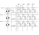
- Itis a circuit diagram which shows the circuit structure of the some pixel and photosensor circuit which were formed on the active matrix substrate of a liquid crystal display device.
- Itis a schematic block diagram which shows the structure of a liquid crystal display device.
- FIG. 2is a process diagram sequentially illustrating manufacturing steps of the circuit board illustrated in FIG. 1.
- FIG. 3is a process diagram sequentially illustrating manufacturing steps of the circuit board illustrated in FIG. 2. It is a block diagram which shows the schematic structure of the liquid crystal display device of this embodiment.
- FIG. 9is a circuit diagram illustrating a circuit configuration of a protection circuit and a pixel circuit formed in a region Sb illustrated in FIG. 8. It is a circuit diagram which shows the other circuit structure of the said protection circuit. It is a circuit diagram which shows the bidirectional
- FIG. 13is a schematic cross-sectional view of the protection circuit taken along line A-A ′ shown in FIG. 12. It is sectional drawing which shows the structure of the conventional bottom gate type (reverse stagger type) TFT.
- FIG. 1is a cross-sectional view schematically showing a basic configuration of the circuit board 1.
- the circuit board 1is formed on the same insulating substrate 2 corresponding to pixels arranged in a matrix (see FIG. 3) or corresponding to a predetermined group of pixels.
- a plurality of transistor elementsare provided.
- At least one of the plurality of transistor elementsis a first thin film transistor element 10, and the first thin film transistor element 10 includes an oxide semiconductor as a channel layer (also referred to as a semiconductor layer or an active layer) 11.
- the first thin film transistor element 10is referred to as an oxide TFT 10.
- the oxide semiconductoran amorphous oxide material typified by In—Ga—Zn—O is suitable, and a polycrystalline material typified by zinc oxide (ZnO) can also be used.
- At least another one of the plurality of transistor elementsis a second thin film transistor element 20.
- the second thin film transistor element 20includes a hydrogenated amorphous silicon semiconductor (a-Si: H) as a channel layer 21 and has a circuit role different from that of the oxide TFT 10.
- the second thin film transistor element 20is hereinafter referred to as a-Si TFT 20.
- the constituent material of the channel layer 21is not limited to an amorphous silicon semiconductor, but a microcrystalline silicon semiconductor (microcrystalline silicon semiconductor, that is, ⁇ c-Si), or a stacked semiconductor in which a-Si: H and ⁇ c-Si are stacked. Can be adopted. Since the laminated semiconductor can cover a wavelength band that cannot be received by one layer, a highly sensitive photosensor element can be formed for a wide wavelength band.
- the oxide TFT 10can obtain a high output voltage without increasing its size (mobility is about 20 times that of the a-Si TFT), so that it can suppress a decrease in the aperture ratio of the pixel, but light ( In particular, it has a first characteristic of low sensitivity to visible light).
- the a-Si TFT 20has a second characteristic that the output voltage is low because the sensitivity to light is high but the mobility is low.
- the oxide TFT 10 having the first characteristic and the a-Si TFT 20 having the second characteristiccan play different roles in terms of circuit. Therefore, according to said structure, the circuit board 1 with the sufficient performance which mounted the electric circuit using each of the said different role can be obtained.
- FIG. 3is a circuit diagram showing a circuit configuration of the plurality of pixels 30 and the photosensor circuit 40 formed on the active matrix substrate of the liquid crystal display device. This active matrix substrate corresponds to the circuit substrate 1. Among these, the above basic configuration of the circuit board 1 is applied to the optical sensor circuit 40.
- FIG. 3shows a circuit configuration built in the region Sa shown in the display panel 51 provided in the liquid crystal display device 50 described later with reference to FIG.
- the optical sensor circuit 40will be schematically described. As shown in FIG. 3, the oxide TFT 10 and the a-Si TFT 20 constitute the optical sensor circuit 40, and the oxide TFT 10 includes the optical sensor circuit 40.
- the a-Si TFT 20serves as a sensor output (output amplifier), and serves as a photo sensor element of the photo sensor circuit 40.
- the optical sensor circuit 40is configured as a 1T (abbreviation of transistor) type circuit using only one transistor that plays a role of sensor output.
- the oxide TFT 10functions as a source follower transistor (voltage follower transistor).
- the drain of the oxide TFT 10is connected to the AMP power supply bus line Vsm (m is a natural number indicating the pixel column number), and the source is connected to the photosensor output bus line Vom + 1.
- the AMP power supply bus line Vsm and the optical sensor output bus line Vom + 1are connected to the sensor readout circuit 55 shown in FIG. 4, and the power supply voltage VDD is applied from the sensor readout circuit 55 to the AMP power supply bus line Vsm. .
- the source of the a-Si TFT 20 functioning as a photodiodeis connected to the base of the oxide TFT 10 and one end of a boosting capacitor 41 is connected to the base of the oxide TFT 10.
- the drain electrode 26 of the a-Si TFT 20is short-circuited to the gate electrode 22 (base). That is, as shown in FIG. 3, the a-Si TFT 20 has a diode-connected configuration, and functions as a photodiode having the source electrode 25 as a cathode and the drain electrode 26 as an anode.
- the drain of the a-Si TFT 20is connected to a photodiode reset wiring Vrstn (n is a natural number indicating a pixel row number) to which a reset signal RST is sent from the sensor scanning signal line drive circuit 54 shown in FIG.
- the other end of the capacitor 41is connected to an optical sensor row selection wiring Vrwn to which an optical sensor row selection signal RWS is sent.
- the photosensor row selection signal RWShas a role of selecting a specific row of photosensor circuits arranged in a matrix and outputting a detection signal from the photosensor circuit 40 in the specific row.
- the oxide TFT 10can obtain a high output voltage without increasing its size, so that it can suppress a decrease in the aperture ratio of the pixel, but has the first characteristic that the sensitivity to light is low. Therefore, it is suitable for the role of the sensor output of the optical sensor circuit 40.
- the a-Si TFT 20is suitable for the role of the photosensor element of the photosensor circuit 40 because it has the second characteristic that the output voltage is low because of its low mobility but high sensitivity to light.
- the optical sensor elementis required to have sensitivity to any wavelength band of the ultraviolet light region, the visible light region, and the infrared light region.
- a-Si: Hhas a good sensitivity over almost the entire visible light region so as to have a sensitivity peak in the vicinity of 500 to 600 nm.
- the oxide TFT 10 and the a-Si TFT 20can constitute the photosensor circuit 40 having excellent advantages of suppressing the decrease in aperture ratio of the pixel, high sensitivity, and high response speed.
- ⁇ c-Si or a laminated semiconductor in which a-Si: H and ⁇ c-Si are laminatedis used for the channel layer 21 of the a-Si TFT 20.
- an excellent advantage of such a photosensor circuit 40is that, for example, by mounting a plurality of photosensor circuits 40 in an active matrix substrate in which pixels using liquid crystals are arranged in a matrix, a touch panel function or an image can be obtained. This is extremely advantageous when a liquid crystal display device having a scanner function or the like is configured.
- optical sensor circuit 40The operation of the optical sensor circuit 40 will be described later.
- a gate wiring Gn and a source wiring Smare further formed in a matrix on the circuit board 1 on which the photosensor circuit 40 is provided.
- Well-known elements constituting the pixel 30are formed, such as a switching element for driving the pixel 30, a pixel electrode for forming a liquid crystal capacitor, and an auxiliary capacitor.
- the auxiliary capacitance of each pixel 30is connected to the auxiliary capacitance line Csn.
- the same number of photosensor circuits 40 as that of all the pixels 30may be provided, or a predetermined number of groups of pixels 30 may be provided.
- the number of photosensor circuits 40may be determined according to the balance with the resolution required for photodetection.
- one photosensor circuit 40is provided for three pixels 30.
- three pixels of R (red), G (green), and B (blue) corresponding to full color displaycan be assigned.
- the source line Smalso serves as the AMP power supply bus line Vsm, and the source line Sm + 1 adjacent to the source line Sm also serves as the photosensor output bus line Vom + 1.
- the oxide TFT 10 and the a-Si TFT 20are both configured as bottom-gate transistors.
- the oxide TFT 10includes a gate electrode 12 as a bottom gate, and a first gate insulating film (first insulating layer) 3 mainly composed of SiO 2 covers the gate electrode 12. .
- the channel layer 11is formed on the first gate insulating film 3, and the etching stopper 14 mainly composed of SiO 2 is stacked on the channel layer 11.
- a source electrode 15 that covers each side surface on the source side of the channel layer 11 and the etching stopper 14is formed in a range from the upper surface of the first gate insulating film 3 to the upper surface of the etching stopper 14.
- the drain electrode 16 covering the drain side surface of the channel layer 11 and the etching stopper 14is formed in a range from the upper surface of the first gate insulating film 3 to the upper surface of the etching stopper 14.
- the a-Si TFT 20includes a gate electrode 22 as a bottom gate, and the gate electrode 22 is covered with the first gate insulating film 3 shared with the oxide TFT 10.
- a second gate insulating film (second insulating layer) 23mainly composed of SiN X is locally formed on the first gate insulating film 3, and the second The channel layer 21 is formed on the gate insulating film 23.
- a conductive layer 24 separated into a source side and a drain sideis stacked.
- n + a-Si or n + ⁇ c-Si doped with a relatively high concentration of n-type impuritiescan be used.
- the source electrode 25 covering the side surfaces on the source side of the second gate insulating film 23, the channel layer 21, and the conductive layer 24extends from the upper surface of the first gate insulating film 3 to the upper surface of the conductive layer 24 on the source side. Formed in a range.
- the drain electrode 26 covering each side surface on the drain side of the second gate insulating film 23, the channel layer 21, and the conductive layer 24extends from the upper surface of the first gate insulating film 3 to the upper surface on the drain side of the conductive layer 24. It is formed in a wide range.
- the oxide TFT 10 and the a-Si TFT 20are covered and protected by a passivation film 4 containing SiN X as a main component.
- the drain electrode 26 of the a-Si TFT 20is short-circuited with the gate electrode 22 through a through hole formed in the first gate insulating film 3.
- the insulating film included in the a-Si TFT 20has a two-layer structure of the first gate insulating film 3 and the second gate insulating film 23.
- the insulating film included in the oxide TFT 10may have a two-layer structure, contrary to the configuration of FIG.
- FIG. 2is a cross-sectional view schematically showing a modification of the basic configuration of the circuit board shown in FIG.
- symbolis attached
- a circuit board 1A shown in FIG. 2includes an oxide TFT 10A and an a-Si TFT 20A both configured as bottom-gate transistors.
- the oxide TFT 10Aincludes a gate electrode 12 as a bottom gate, and a first gate insulating film (first insulating layer) 3A mainly composed of SiN X covers the gate electrode 12. .
- a second gate insulating film (second insulating layer) 23A mainly composed of SiO 2is locally formed on the first gate insulating film 3, and on the second gate insulating film 23A, The channel layer 11 and the etching stopper 14 are formed in this order.
- the source electrode 15 and the drain electrode 16are the same as those in FIG. 1 except that they are provided on the second gate insulating film 23A.
- the a-Si TFT 20Aalso includes a gate electrode 22 as a bottom gate, and the gate electrode 22 is covered with the first gate insulating film 3A shared with the oxide TFT 10A.
- the configurationis the same as that of the a-Si TFT 20 except that the second gate insulating film 23 is removed from the a-Si TFT 20 of FIG.
- the oxide TFT 10A and the a-Si TFT 20Aare also covered and protected by the passivation film 4 mainly composed of SiN X , which is the same as the configuration of FIG.
- the drain electrode 26 of the a-Si TFT 20Ais short-circuited with the gate electrode 22 through a through hole formed in the first gate insulating film 3A.
- both the oxide TFT 10 and the a-Si TFT 20 or the oxide TFT 10A and the a-Si TFT 20Aare bottom gate type, for example, a backlight is provided, and the emitted light intensity of the backlight is modulated by the pixel 30.
- the gate electrodes 12 and 22can shield the light emitted from the backlight. In particular, it is possible to prevent the characteristics of the oxide TFT 10 or the oxide TFT 10A from being deteriorated without providing a light shielding film.
- the gate electrode 12 and the gate electrode 22are formed by the same conductive layer (patterning), and the source electrode 15, 25 and the drain electrodes 16 and 26 are formed by the same conductive layer (patterning).
- the aperture ratio of the pixel 30is suppressed from being lowered, high sensitivity, and high response speed are excellent.
- the manufacturing processcan be simplified and the cost can be reduced without deteriorating the advantages.
- the channel layer 11 of the oxide TFT 10includes the first gate insulating film 3 mainly composed of oxide-based SiO 2 and the etching stopper mainly composed of SiO 2. 14.
- the channel layer 21 of the a-Si TFT 20has a two-layer structure of SiN X / SiO 2 as a gate insulating film of the a-Si TFT 20, and as a result, a second gate insulating film mainly composed of nitride-based SiN X. 23 and a passivation film 4 containing SiN X as a main component.
- circuit board 1Athe results for the gate insulating film of the oxide TFT10 a two-layer structure of SiO 2 / SiN X, oxide channel layer 11 of the TFT10, the second mainly of SiO 2 oxide
- the gate insulating film 23A and the etching stopper 14 mainly composed of SiO 2are sandwiched.
- the channel layer 21 of the a-Si TFT 20Ais sandwiched between the first gate insulating film 3A mainly composed of nitride-based SiN X and the passivation film 4 mainly composed of SiN X.
- the first gate insulating film 3is formed as the same layer common to the oxide TFT 10 and the a-Si TFT 20, and the first gate insulating film 3A is the same layer common to the oxide TFT 10A and the a-Si TFT 20A. It is formed as.
- the oxide semiconductor constituting the channel layer 11 and the amorphous silicon semiconductor constituting the channel layer 21can be in contact with a gate insulating film or a passivation film suitable for each.
- a reducing materialhere, hydrogenated a-Si forming the channel layer 21 and SiN x forming the passivation film 4
- the oxide semiconductoris reduced and its characteristics deteriorate.
- the oxidesince the oxide is in contact with the oxide semiconductor, the characteristics can be prevented from being deteriorated.
- the manufacturing processcan be further simplified and the cost can be reduced.
- FIG. 4is a schematic block diagram showing the configuration of the liquid crystal display device 50.
- the liquid crystal display device 50includes a display panel 51, a display scanning signal line driving circuit 52, a display video signal line driving circuit 53, a sensor scanning signal line driving circuit 54, a sensor readout circuit 55, a sensing image.
- a processing unit 56 and a power supply circuit 57are provided.
- the display panel 51includes an active matrix substrate and a counter substrate sealed with a liquid crystal layer interposed therebetween.
- the insulating substrate 2 shown in FIG. 1is a base member of an active matrix substrate, for example, a glass substrate.
- the circuits constituting the display scanning signal line driving circuit 52, the display video signal line driving circuit 53, the sensor scanning signal line driving circuit 54, and the sensor readout circuit 55have a separately created LSI mounted on the display panel 51. Alternatively, it may be monolithically formed on the insulating substrate 2.
- “Monolithically formed”means that a circuit element is formed directly on the insulating substrate 2 by at least one of a physical process and a chemical process, and the semiconductor circuit is mounted on the glass substrate as a module. Does not include that.
- the liquid crystal display device 50When the liquid crystal display device 50 is a VA (Vertical Alignment) mode liquid crystal display device, a common electrode and R (red), G (green), and B (blue) color filters are provided on the counter substrate. . Since the present invention is not limited by the liquid crystal mode, it can also be applied to a TN (Twisted Nematic) mode, and further, an IPS (In-Plane Switching) also called a lateral electric field application method in which a common electrode is provided on an active matrix substrate. ) Mode.
- VAVertical Alignment
- a common electrode and R (red), G (green), and B (blue) color filtersare provided on the counter substrate.
- TNTransmission Nematic
- IPSIn-Plane Switching
- the display scanning signal line driving circuit 52uses the gate wiring Gn to generate a scanning signal for selectively scanning the pixels 30 row by row.
- the display video signal line drive circuit 53supplies a video signal to each pixel 30 using the source line Sm.
- the sensor scanning signal line drive circuit 54selects and drives the optical sensor circuit 40 row by row, and the sensor readout circuit 55 uses the AMP power supply bus line Vsm to supply the optical sensor circuit 40 with the constant potential.
- a power supply voltage VDDis supplied, and a photodetection signal is read from the photosensor circuit 40 using the photosensor output bus line Vom + 1.
- the sensing image processing unit 56is configured by an LSI (Large Scale Integrated Circuit), a PC (Programmable Controller), or the like, and scans an original from a light detection signal output from the optical sensor circuit 40 according to a stored image processing program. Alternatively, information such as the position of a finger or a pointing pen with respect to the display panel 2 is generated.
- LSILarge Scale Integrated Circuit
- PCComputer Controller
- the power supply circuit 57supplies necessary power supply voltages to the circuits 52 to 56, respectively.
- the configuration of the liquid crystal display device 50is not limited to the above-described configuration, and the sensor scanning signal line drive circuit 54 or the sensor readout circuit 55 is another circuit, specifically, a display scanning signal line drive circuit. 52 or the display video signal line drive circuit 53 or the like may be included as a function, and the sensor readout circuit 55 may be included in the function of the sensing image processing unit 56.
- FIG. 5is a timing chart showing the operation of the optical sensor circuit 40.
- the oxide TFT 10 and the a-Si TFT 20will be described.
- the operation of the optical sensor circuit 40does not change for the oxide TFT 10A and the a-Si TFT 20A.
- a high level reset signal RSTis sent from the sensor scanning signal line drive circuit 54 to the photodiode reset wiring Vrstn.
- the reset period (t1 to t2)since the forward bias is applied to the a-Si TFT 20 as the photodiode, the boosting capacitor 41 is charged, the base potential VINT gradually rises, and finally the initialization potential ( V DDR ) is reached.
- the cathode potential of the a-Si TFT 20(the potential of netA, which is the connection site between the base of the oxide TFT 10 and the source of the a-Si TFT 20) Since this is higher than the anode potential, a reverse bias is applied to the a-Si TFT 20.
- the base potential VINTis obtained by subtracting the forward voltage drop (V F ) in the a-Si TFT 20 and the voltage drop ( ⁇ V RST ) caused by the parasitic capacitance of the a-Si TFT 20 from the initialization potential (V DDR ). Value.
- the light detection result reading periodthat is, the detection signal reading period (t3 to t4) is entered, and then the optical sensor row selection wiring Vrwn is connected from the sensor scanning signal line driving circuit 54 to the other end of the boosting capacitor 41.
- a high-level row selection signal RWSis applied through this.
- the base potential VINTis pushed up through the boosting capacitor 41. Therefore, the base potential VINT is a potential obtained by adding the high level potential of the row selection signal RWS to the detection potential (for example, the potential V1 shown in FIG. 5). become.
- the potential V1 shown in FIG. 5corresponds to the bright state when the a-Si TFT 20 receives strong light and the base potential VINT drops to the lowest level at t3.
- the threshold voltage for turning on the oxide TFT 10is exceeded, so that the oxide TFT 10 is turned on.
- a voltage controlled with an amplification factor according to the level of the base potential VINTthat is, according to the light intensity, is detected from the source of the oxide TFT 10 as a detection signal (for example, the bright state VPIX shown in FIG. 5). Is output and sent to the sensor readout circuit via the optical sensor output bus line Vom + 1.
- the base potential VINTis pushed up through the boosting capacitor 41 in the same manner as described above, so that the base potential VINT is set to the initialization potential and the high level of the row selection signal RWS.
- the potential of the levelbecomes substantially equal to the added potential (for example, the potential V2 shown in FIG. 5).
- the detection signal output from the oxide TFT 10(for example, VPIX in the dark state shown in FIG. 5) shows the maximum level.
- a detection signal having a level corresponding to the intensity of light received by the a-Si TFT 20is generated, and the detection signal is generated in the pixel 30 corresponding to the photosensor circuit 40. Therefore, using the light of the backlight provided in the liquid crystal display device 50 shown in FIG. 4 as a light source for display, the coordinates on the display panel 51 can be read with respect to the detection target arranged close to the display panel 51, Detection operations such as character reading or fingerprint reading can be performed.
- the optical sensor circuit 40is configured by an extremely small number of elements as compared with the conventional CMOS optical sensor circuit. For this reason, since the area occupied by the photosensor circuit 40 is reduced, the 1T photosensor circuit 40 is very advantageous for increasing the aperture ratio of the pixel 30. In addition, if the number of elements is small, the self-parasitic capacitance of the optical sensor circuit 40 is reduced, so that the response speed of the detection operation is increased, and the problem that the dynamic range is reduced by pulling in the parasitic capacitance can be improved. it can.
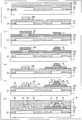
- FIG. 6is a process diagram showing the manufacturing process of the circuit board 1 in order.
- the method for manufacturing a circuit board according to the present inventionis different in that the oxide TFT 10 and the a-Si TFT 20 have different circuit roles due to different types of semiconductors forming the channel layers 11 and 21. Is a manufacturing method for forming on the same insulating substrate 2.
- step Athe gate electrodes 12 and 22 of the oxide TFT 10 and the a-Si TFT 20 are simultaneously formed by patterning the same conductive layer formed on the insulating substrate 2 (step A).
- This step Acorresponds to the first step described in the claims.
- the first gate insulating film 3 mainly composed of SiO 2 which is an insulating material suitable for an oxide semiconductor (not deteriorated)is formed on each of the gate electrodes 12 and 22 (step B). .
- SiN Xwhich is an insulating material suitable for an amorphous silicon semiconductor (not deteriorated), is mainly formed on the first gate insulating film 3.
- the second insulating film 23ais stacked (step C), and the a-Si film 21a and the conductive film 24a are stacked in this order (step D).
- the conductive film 24ais an n + a-Si or n + ⁇ c-Si film in which an n-type impurity is doped at a relatively high concentration.
- step Ethe second insulating film 23a, the a-Si film 21a and the conductive film 24a are patterned together (step E), and the second for the a-Si TFT 20 is patterned.
- a conductive layer 24b before forming the gate insulating film 23, the channel layer 21, and the conductive layer 24is formed (step F).
- an oxide semiconductoris formed on the first gate insulating film 3 and patterned to form the channel layer 11 of the oxide TFT 10 (step G).
- the etching stopper 14is formed by forming and patterning a film mainly containing SiO 2 on the channel layer 11 (step H).
- a contact hole 3ais formed in the first gate insulating film 3, and the gate electrode 22 is locally exposed (see FIG. 6E). Step I).
- a conductive layeris formed on the entire surface and patterned to form the source electrodes 15 and 25 and the drain electrodes 16 and 26 of the oxide TFT 10 and the a-Si TFT 20 simultaneously from the same conductive layer (step J).
- the conductive layer 24bis etched, a gap is formed in the conductive layer 24b, and the conductive layer 24 is formed (step K).
- the process Jcorresponds to the third process described in the claims.
- step Lthe entire surface is covered with the passivation film 4 (step L), and the circuit board 1 is completed.
- the first gate insulating film 3is simultaneously formed as the same layer shared by the oxide TFT 10 and the a-Si TFT 20, and thereafter, SiN X Is formed, and the gate insulating film of the a-Si TFT 20 has a two-layer structure of SiO 2 / SiN X. Therefore, the manufacturing process is not complicated and can be simplified, and the cost can be reduced. You can go down.
- the gate electrodes 11 and 22 of the oxide TFT 10 and the a-Si TFT 20are formed by the same conductive layer, and the source electrodes 15 and 25 and the drain electrodes 16 and 26 are also formed by the same conductive layer. ing. Thereby, the manufacturing process can be further simplified and the cost can be reduced.
- FIG. 7is a process diagram showing the manufacturing process of the circuit board 1A in order.
- the process A for simultaneously forming the gate electrodes 12 and 22 on the insulating substrate 2is as described above.
- the conductive film 24ais an n + a-Si or n + ⁇ c-Si film in which an n-type impurity is doped at a relatively high concentration.
- step D ′the a-Si film 21a and the conductive film 24a are patterned together (step D '), and the channel layer 21 and the conductive layer 24 for the a-Si TFT 20A are formed.
- the previous conductive layer 24bis formed (step E ′).
- a second main component of SiO 2 that is an insulating material suitable for an oxide semiconductor (not deteriorated)is formed on the first gate insulating film 3A.
- An insulating film 23bis stacked (step F ′).
- an oxide semiconductoris formed on the second insulating film 23b and patterned to form the channel layer 11 of the oxide TFT 10A (step G ′).
- the etching stopper 14is formed by forming and patterning a film mainly composed of SiO 2 on the channel layer 11 (step H ′).
- the second insulating film 23bis removed from the a-Si TFT 20A by using, for example, a photolithography technique to thereby form the first and second channel layers 11 of the oxide TFT 10A.
- the second gate insulating film 23Ais locally formed between the gate insulating film 3A (step I ′).
- the step of forming the diode connection of the a-Si TFT 20A, the source electrodes 15 and 25 of the oxide TFT 10A and the a-Si TFT 20A, and the drain electrodes 16 and 26are connected to the same conductive layer.
- the steps of forming the conductive layer 24 simultaneously, the step of forming the conductive layer 24 of the a-Si TFT 20A, and the step of forming the passivation film 4 shown in FIG. 7Gare as described above with reference to FIG. In this way, the circuit board 1A is completed.
- the first gate insulating film 3is simultaneously formed as the same layer shared by the oxide TFT 10 and the a-Si TFT 20, and thereafter, SiO 2 Is formed, and the gate insulating film of the oxide TFT 10A has a two-layer structure of SiN x / SiO 2 , so that the manufacturing process is not complicated and can be simplified. Cost can be reduced.
- the gate electrodes 11 and 22 of the oxide TFT 10A and the a-Si TFT 20Aare formed by the same conductive layer, and the source electrodes 15 and 25 and the drain electrodes 16 and 26 are also formed by the same conductive layer. ing. Thereby, the manufacturing process can be further simplified and the cost can be reduced.
- FIG. 8is a block diagram showing a schematic configuration of the liquid crystal display device 50a of the present embodiment.
- the liquid crystal display device 50aincludes a display panel 51a obtained by removing the optical sensor circuit 40 from the display panel 51, the display scanning signal line drive circuit 52, the display video signal line drive circuit 53, the drive circuits 52, and And a power supply circuit 57 a for supplying a necessary power supply voltage to the power supply 53.
- the configuration of the liquid crystal display device 50ais not limited to the configuration example shown in FIG.
- the liquid crystal display device 50ais provided with a protection circuit between the display scanning signal line drive circuit 52 and the pixel circuit for protecting the thin film elements constituting the pixel circuit in the display panel 51a from external noise.
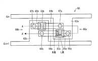
- FIG. 9is a circuit diagram showing a circuit configuration of the protection circuit 60 and the pixel circuit 70 formed in the region Sb shown in FIG.
- the first transistor element(for example, the pixel driving TFT 71 of the pixel circuit 70) which is a part of the plurality of transistor elements provided on the same insulating substrate is protected in a circuit manner.
- the protection circuit 60includes a protection circuit 60 including a second transistor element (for example, a TFT functioning as the diode 61) that is a part of the plurality of transistor elements.
- the first transistor elementis made of an oxide TFT
- the second transistor elementis made of an a-Si TFT.
- an a-Si TFTis used for an element that requires high resistance (for example, a protection element), and an oxide semiconductor is used for an element that preferably has low resistance (high mobility) (for example, a switching element).
- a TFT in which a channel layer is formed by ⁇ c-Si or a stacked semiconductor in which a-Si: H and ⁇ c-Si are stackedcan be employed.
- the protection circuit 60is a bidirectional diode configured by connecting diodes 61 whose forward directions are opposite to each other in parallel, and one protection circuit 60 is provided for every gate wiring Gn. It is provided one by one. Such a protection circuit 60 is also called a diode short ring. One end of the protection circuit 60 is connected to the gate line Gn, and the other end is connected to, for example, a ground line.
- the bidirectional diodecan cope with an excessive voltage of both positive and negative polarities.
- the protection circuit 60may be provided so as to connect the gate wiring Gn and the gate wiring Gn + 1 adjacent to each other. In this case, since an excessive voltage applied to one gate line Gn can be distributed to other gate lines, the pixel circuit 70 can be similarly protected.
- the TFT functioning as the diode 61 of the protection circuit 60is an a-Si TFT, ⁇ c-Si, or a TFT using the laminated semiconductor. This is effective in reducing the area occupied by the protection circuit 60 and reducing the frame size of the display panel 51a.
- the oxide TFThas a characteristic that the on-resistance is one digit smaller than that of the a-Si TFT. For this reason, when an oxide TFT is used in the protection circuit 60 of FIG. 9, there is a risk of current leakage between the gate line Gn and the ground line, and the oxide TFT is added to the protection circuit 60 of FIG. If used, current leakage may occur between adjacent gate wirings.
- the channel length (L length) of the oxide TFTis increased, thereby increasing the on-resistance of the oxide TFT. It becomes necessary to do. For this reason, the size of the oxide TFT must be increased, which hinders the narrowing of the frame of the display panel 51a.
- the protective circuit 60is not provided in preference to narrowing the frame of the display panel 51a, dielectric breakdown or the like occurs in the pixel circuit 70, and the manufacturing yield of the display panel 51a decreases.
- thin film transistorsthat play different roles on the same insulating substrate
- thin film transistors having optimum characteristicsare adopted according to their roles, so that the performance of the circuit board can be maximized. it can.
- the main operationis performed like a switching element of each pixel of a liquid crystal display device or a transistor element included in a driving circuit monolithically formed on the same insulating substrate as the switching element. Since the transistor element to be performed is an oxide TFT, responsiveness or driving capability can be increased.
- the transistor element constituting the protection circuitis an a-Si TFT, the display panel can be narrowed, contributing to downsizing of the display device.
- the protection circuit 60can be provided in the source wiring Sm as disclosed in the above-mentioned Patent Document 5, and is not limited to the forms shown in FIGS.
- FIG. 11is a circuit diagram showing a bidirectional diode constituting the protection circuit 60 using TFT circuit symbols. As shown in FIG. 11, of the two TFTs 60a and 60b whose drain and gate are short-circuited, the gate of the TFT 60a is connected to the gate wiring Gn, the gate of the TFT 60b is connected to the adjacent gate wiring Gn + 1, , Each source is connected to the other's gate.
- FIG. 12is a schematic plan view of the protection circuit 60 and the TFT.
- the gate electrode 62aextends from the gate wiring Gn to the gate wiring Gn + 1, and on the channel layer 63a of the a-Si semiconductor provided above the gate electrode 62a, the source electrode 64a and the drain electrode 65a are opposed to each other with a gap therebetween.
- the drain electrode 65ais connected to the gate electrode 62a through the contact hole 66a.
- the source electrode 64ais connected to the gate electrode 62b of the TFT 60b through the contact hole 66b.
- the gate electrode 62bextends from the gate wiring Gn + 1 to the gate wiring Gn, and on the channel layer 63b of the a-Si semiconductor provided above the gate electrode 62b, the source electrode 64b and the drain electrode 65b is opposed to each other with a gap.
- the drain electrode 65bis connected to the gate electrode 62b through the contact hole 67b.
- the source electrode 64ais connected to the gate electrode 62a of the TFT 60a through the contact hole 67a.
- the channel layer 63a and the channel layer 63bare both formed of an a-Si semiconductor, even if the channel width (W length) shown in FIG. 12 is the same as that of the oxide TFT, the channel length (L length) is The required on-resistance can be obtained by making it shorter than the oxide TFT.
- FIG. 13is a schematic cross-sectional view of the protection circuit 60 taken along the line AA ′ shown in FIG. As shown in FIG. 13, the TFTs 60 a and 60 b are formed on the same insulating substrate 2 and covered and protected by the passivation film 4.
- gate electrodes 62a and 62bare formed on the insulating substrate 2, and the first gate insulating film 3 covers the gate electrodes 62a and 62b.
- Second gate insulating films 23C and 23D corresponding to the second gate insulating film 23are stacked on the first gate insulating film 3 at positions above the gate electrodes 62a and 62b, respectively.
- a-Si semiconductor channel layers 63a and 63bare stacked on the second gate insulating films 23C and 23D, respectively.
- Conductive layers 68a and 68b with gapsare stacked on the channel layers 63a and 63b, and a source electrode 64a and a drain electrode 65a facing each other with a gap are formed on the conductive layer 68a.
- a source electrode 64b and a drain electrode 65b facing each other with a gapare formed.
- the source electrode 64aextends on the gate electrode 62b of the TFT 60b and is connected to the gate electrode 62b through a contact hole 66b.
- the drain electrode 65ais connected to its own gate electrode 62a through a contact hole 66a.
- the source electrode 64bextends onto the gate electrode 62a of the TFT 60a and is connected to the gate electrode 62a through the contact hole 67a.
- the drain electrode 65bis connected to its own gate electrode 62b through a contact hole 67b.
- the gate electrode of the first thin film transistor element and the gate electrode of the second thin film transistor elementare formed of the same conductive layer
- the source electrode and the drain electrode of the first thin film transistor element and the source electrode and the drain electrode of the second thin film transistor elementare formed of the same conductive layer.
- the circuit boardwhen the circuit board is mounted on a backlight type display device, the excellent advantages of suppressing the decrease in the aperture ratio of the pixel and having a high response speed are not deteriorated.
- the manufacturing processcan be simplified, and a remarkable effect that costs can be reduced can be obtained.
- the circuit boardwhen the circuit board is mounted on a display device including a second thin film transistor element that functions as an optical sensor element, the excellent advantage of high sensitivity to light to be sensed is not impaired, or When the circuit board is mounted on a display device including a second thin film transistor element that functions as a circuit element constituting the protection circuit, as described above, the occupation area of the protection circuit is reduced, The excellent advantage of reducing the frame size of the display device is not impaired, and the manufacturing process can be simplified and the cost can be reduced.
- a gate insulating film mainly composed of SiO 2is sandwiched between the channel layer and the gate electrode of the first thin film transistor element, (8) Between the channel layer and the gate electrode of the second thin film transistor element, a gate insulating film mainly composed of SiN X and a gate insulating film mainly composed of SiO 2 are sequentially laminated from the channel layer side. Being pinched, (9) The SiO 2 layer common to both gate insulating films is formed as the same layer.
- a gate insulating film mainly composed of SiO 2 and a gate insulating film mainly composed of SiN Xare laminated in this order from the channel layer side. Being pinched, (11) A gate insulating film mainly composed of SiN X is sandwiched between the channel layer and the gate electrode of the second thin film transistor element, (12) The SiN X layer common to both gate insulating films is formed as the same layer.
- the oxide semiconductor constituting the channel layer of the first thin film transistor element and the channel layer of the second thin film transistor elementare constituted.
- Gate insulation suitable for (a) an amorphous silicon semiconductor, (b) a microcrystalline silicon semiconductor, or a semiconductor in which these (a) and (b) semiconductors are stacked(hereinafter referred to as a non-oxide semiconductor). Can contact the membrane.
- the manufacturing processcan be simplified and the cost can be reduced.
- the first thin film transistor element and the second thin film transistor elementconstitute an optical sensor circuit
- the first thin film transistor elementserves as a sensor output of the optical sensor circuit
- the second thin film transistor elementplays a role of an optical sensor element of the optical sensor circuit.
- the first thin film transistor element including the oxide semiconductor as a channel layercan obtain a high output voltage without increasing the size, and thus can suppress a decrease in the aperture ratio of the pixel, but has a sensitivity to light. Since it has the first characteristic of being low, it is suitable for the role of the sensor output of the optical sensor circuit.
- the second thin film transistor element including the non-oxide semiconductor as a channel layerhas high sensitivity to light, but has a second characteristic that output voltage is low because of low mobility. It is suitable for the role of the optical sensor element.
- the first thin film transistor element and the second thin film transistor elementcan constitute an optical sensor circuit having excellent advantages of suppressing the decrease in aperture ratio of the pixel, high sensitivity, and high response speed.
- an excellent advantage of such a photosensor circuitis that, for example, a plurality of photosensor circuits are mounted on an active matrix substrate in which pixels using liquid crystals are arranged in a matrix, thereby enabling a touch panel function or an image scanner function. This is extremely advantageous when a liquid crystal display device including the above is configured.
- a protection circuit for circuit-protecting the first transistor element that is a part of the plurality of transistor elementsincluding a second transistor element that is a part of the plurality of transistor elements Including
- the first transistor elementincludes the first thin film transistor element.
- the second transistor elementincludes the second thin film transistor element.
- the second transistor element included in the protection circuitis the second thin film transistor element including the non-oxide semiconductor as a channel layer, so that the second transistor element is an oxide semiconductor.
- the area occupied by the protection circuitcan be reduced.
- the first transistor element that is protected in terms of the circuitis the first thin film transistor element, for example, the switching element of each pixel of the liquid crystal display device or a monolithic on the same insulating substrate as the switching element.
- the transistor elements included in the driving circuit formed in the abovethe responsiveness or driving capability of the transistor elements that perform the main operation can be increased.
- a display deviceincludes any one of the circuit boards described above.
- the second step in the method of manufacturing a circuit board according to the present inventionincludes: (23) forming a first insulating layer covering each gate electrode using an insulating material suitable for a semiconductor forming a channel layer of the first thin film transistor element; (24) Using the insulating material suitable for the semiconductor forming the channel layer of the second thin film transistor element, the first insulating layer at a position corresponding to the position where the channel layer of the second thin film transistor element is formed. And a step of locally forming a second insulating layer thereon.
- the second step in the method for manufacturing a circuit board of the present inventionincludes: (25) forming a first insulating layer covering each of the gate electrodes using an insulating material suitable for a semiconductor forming a channel layer of the second thin film transistor element; (26) The first insulating layer is formed at a position corresponding to the position where the channel layer of the first thin film transistor element is formed using an insulating material suitable for a semiconductor forming the channel layer of the first thin film transistor element. And a step of locally forming a second insulating layer thereon.
- the present inventioncan be applied to a circuit board on which a plurality of TFTs having different types of semiconductor layers are mounted, and an electronic device such as a display device on which the circuit board is mounted.
Landscapes
- Physics & Mathematics (AREA)
- Nonlinear Science (AREA)
- Mathematical Physics (AREA)
- Chemical & Material Sciences (AREA)
- Crystallography & Structural Chemistry (AREA)
- General Physics & Mathematics (AREA)
- Optics & Photonics (AREA)
- Engineering & Computer Science (AREA)
- Microelectronics & Electronic Packaging (AREA)
- Thin Film Transistor (AREA)
- Liquid Crystal (AREA)
- Metal-Oxide And Bipolar Metal-Oxide Semiconductor Integrated Circuits (AREA)
Abstract
Description
Translated fromJapanese本発明は、薄膜トランジスタを搭載した回路基板と、その回路基板を備えた表示装置と、その回路基板の製造方法とに関するものである。The present invention relates to a circuit board on which a thin film transistor is mounted, a display device including the circuit board, and a method for manufacturing the circuit board.
薄膜トランジスタ(TFT)は、例えば液晶表示装置(LCD)の画素のスイッチングを司る回路素子、あるいはLCDのドライバを構成する回路素子などの用途に広く用いられてきた。近年では、LCDに要求される大画面、高精細および高フレームレートなどの性能向上を達成するために、TFTに対しても、高性能および高信頼性が益々求められている。Thin film transistors (TFTs) have been widely used for applications such as circuit elements that control switching of pixels of a liquid crystal display device (LCD) or circuit elements that constitute LCD drivers. In recent years, high performance and high reliability are increasingly required for TFTs in order to achieve performance improvements such as large screen, high definition, and high frame rate required for LCDs.
TFTの高性能および高信頼性の追求に伴い、チャネル層を構成することが可能な半導体の種類に応じて、TFTの種類は多様化している。その中で、単結晶シリコンTFT,非晶質(アモルファス)シリコン(a-Si)TFT,多結晶シリコン(poly-Si)TFTについては、量産技術が確立され、微結晶シリコン(μc-Si)TFT、酸化物TFT、有機TFTの研究開発が活発に進められている。With the pursuit of high performance and high reliability of TFTs, the types of TFTs are diversified according to the types of semiconductors that can constitute the channel layer. Among them, mass production technology has been established for single crystal silicon TFTs, amorphous silicon (a-Si) TFTs, and polycrystalline silicon (poly-Si) TFTs, and microcrystalline silicon (μc-Si) TFTs. Research and development of oxide TFTs and organic TFTs are actively underway.
下掲の特許文献1には、ZnOなどの透明導電性の酸化物半導体をチャネル層に用いたTFTの構成と製造方法とが開示されている。上記酸化物半導体は、低温で成膜でき、かつ可視光に対して透明であるため、プラスチック板やフィルムなどの基板上にフレキシブルな透明TFTを形成することが可能であるとされている。
図14は、従来のボトムゲート型(逆スタガ型)TFTの構造を示す断面図である。当該TFTは、基板101上にゲート電極102を設け、その上に第1の絶縁膜103、チャネル層としての酸化物半導体層104、エッチングストップ層として機能する第2の絶縁膜105、ソース電極106およびドレイン電極107を設けることにより構成される。FIG. 14 is a cross-sectional view showing the structure of a conventional bottom gate type (inverted stagger type) TFT. In the TFT, a
上記酸化物半導体層104として、Inと、Znと、Oとを含むアモルファス酸化物を用いる場合、室温で作製することができるため、絶縁膜にもスパッタ法を用いるならば、すべての成膜工程を室温で形成できる。また、基板としてプラスチック基板やプラスチックフィルムなどを用いることもできる。In the case where an amorphous oxide containing In, Zn, and O is used as the
さらに、上記第2の絶縁膜105がチャネル領域を保護しているため、ソース電極106およびドレイン電極107をドライエッチングはもちろんウェットエッチングによるパターニングで形成することも可能となると特許文献1には記載されている。Further, since the second
なお、下掲の特許文献2には、実施の形態として後述する1トランジスタ型光センサ回路が開示されている。It should be noted that
また、下掲の特許文献3には、非晶質半導体にて形成された受光部を備えた光電変換素子と、多結晶半導体にて形成された半導体層を備えたスイッチング素子とが、透光性基板上に設けられた回路基板が開示されている。
さらに、下掲の特許文献4には、画素表示部中に、非単結晶半導体からなる画素スイッチを備えているとともに、単結晶半導体からなる周辺駆動回路を、上記画素スイッチの駆動用に備えている液晶表示装置が開示されている。Further,
ところが、上記特許文献3および4に開示された構成では、特性の異なるTFTが同一の基板上に設けられているものの、どのTFTもトップゲート型(正スタガ型)TFTである。したがって、特許文献3および4に開示された構成を、画素に対して表示面とは反対側から表示用の光を照射するバックライトタイプの表示装置に適用した場合、表示用の光が半導体層(チャネル層)に直接入射するため、TFTのオフ電流が上昇する問題、経時的な特性変化、または劣化を招く問題が生じる。However, in the configurations disclosed in
また、特許文献3の回路基板を、例えばタッチパネル機能を持たせた表示装置のように、画像表示のためのバックライトの点灯と、タッチ位置を検出するセンシングとを同時に行うことのできる表示装置に適用した場合、表示用の光は、センシングに対しノイズ光となる。In addition, the circuit board of
したがって、表示用の光がチャネル層に直接入射しないようにするには、チャネル層の下層に遮光層が必要となるため、製造工程が長くなりコスト高となる。Therefore, in order to prevent the display light from directly entering the channel layer, a light shielding layer is required under the channel layer, which increases the manufacturing process and increases the cost.
本発明は、上記の問題に鑑みてなされたものであり、その目的は、半導体の種類が異なる複数のTFTが搭載された回路基板の性能を、低コストで充分に発揮させることができる構成と、その製造方法とを提供することにある。The present invention has been made in view of the above-described problems, and the object of the present invention is to be able to sufficiently exhibit the performance of a circuit board on which a plurality of TFTs of different semiconductor types are mounted at low cost. And a manufacturing method thereof.
本発明に係る回路基板は、
(1)マトリクス状に配列された画素に対応して、あるいは上記画素の所定数の一群に対応して、同一の絶縁性基板上に設けられた複数のトランジスタ素子を備え、
(2)上記複数のトランジスタ素子の少なくとも1つは、酸化物半導体をチャネル層として備えた第1の薄膜トランジスタ素子であり、
(3)上記複数のトランジスタ素子の少なくとも他の1つは、(a)非晶質シリコン半導体、(b)微結晶シリコン半導体、またはこれら(a)(b)の半導体を積層した半導体をチャネル層として備えた第2の薄膜トランジスタ素子であり、
(4)上記第1の薄膜トランジスタ素子および第2の薄膜トランジスタ素子が、共にボトムゲート型のトランジスタであることを特徴とする。A circuit board according to the present invention comprises:
(1) A plurality of transistor elements provided on the same insulating substrate corresponding to the pixels arranged in a matrix or corresponding to a predetermined number of groups of the pixels,
(2) At least one of the plurality of transistor elements is a first thin film transistor element including an oxide semiconductor as a channel layer;
(3) At least another of the plurality of transistor elements includes a channel layer formed of (a) an amorphous silicon semiconductor, (b) a microcrystalline silicon semiconductor, or a semiconductor in which these (a) and (b) semiconductors are stacked. A second thin film transistor element provided as
(4) The first thin film transistor element and the second thin film transistor element are both bottom-gate transistors.
上記の構成において、酸化物半導体をチャネル層(半導体層または活性層ともいう)として備えた第1の薄膜トランジスタ素子は、サイズを大きくせずに高い出力電圧が得られるという第1の特性を備えている。In the above structure, the first thin film transistor element including the oxide semiconductor as a channel layer (also referred to as a semiconductor layer or an active layer) has a first characteristic that a high output voltage can be obtained without increasing the size. Yes.
一方、(a)非晶質シリコン半導体、(b)微結晶シリコン半導体、またはこれら(a)(b)の半導体を積層した半導体(非酸化物半導体)をチャネル層として備えた第2の薄膜トランジスタ素子は、光に対する感度が高く、高抵抗という第2の特性を備えている。On the other hand, a second thin film transistor element provided with (a) an amorphous silicon semiconductor, (b) a microcrystalline silicon semiconductor, or a semiconductor (non-oxide semiconductor) in which these (a) and (b) semiconductors are stacked as a channel layer Has high sensitivity to light and has a second characteristic of high resistance.
したがって、それぞれの特性を活かした電気回路を同一の絶縁性基板上に搭載した回路基板を得ることができる。Therefore, it is possible to obtain a circuit board on which an electric circuit utilizing each characteristic is mounted on the same insulating substrate.
上記第1の特性を備えた第1の薄膜トランジスタ素子は、サイズを小さく形成できるので、例えば画素のスイッチング素子、あるいは画素または複数画素に対応して設けられた光センサ回路の出力素子などに好適であり、この場合、画素の開口率の低下を抑制することができる。The first thin film transistor element having the first characteristic can be formed with a small size, and is suitable for, for example, a pixel switching element or an output element of an optical sensor circuit provided corresponding to a pixel or a plurality of pixels. In this case, a decrease in the aperture ratio of the pixel can be suppressed.
上記第2の特性を備えた第2の薄膜トランジスタ素子は、例えば上記光センサ回路の光センサ素子または上記スイッチング素子を回路的に保護する保護回路を構成する回路素子などとして好適である。The second thin film transistor element having the second characteristic is suitable as, for example, a circuit element that constitutes a protection circuit that circuitically protects the optical sensor element of the optical sensor circuit or the switching element.
第2の薄膜トランジスタ素子を上記光センサ素子に適用した場合には、タッチパネル機能を備えた表示装置に好適な回路基板を構成することができる。When the second thin film transistor element is applied to the photosensor element, a circuit board suitable for a display device having a touch panel function can be configured.
この回路基板を、画素に対して表示面とは反対側から表示用の光を照射するバックライトタイプの表示装置に適用した場合、さらに以下の利点を生む。すなわち、表示用の光を各薄膜トランジスタ素子のゲート電極が遮光するので、特に、第1の薄膜トランジスタ素子の特性劣化を、遮光膜を別途設けなくても防止できるという効果が得られる。When this circuit board is applied to a backlight type display device that irradiates display light from the opposite side of the display surface to the pixels, the following advantages are further obtained. That is, since the gate electrode of each thin film transistor element shields the display light, it is possible to particularly prevent the deterioration of the characteristics of the first thin film transistor element without separately providing a light shielding film.
加えて、第2の薄膜トランジスタ素子を用いたセンシングに対しノイズ光となる表示用の光を、ゲート電極によって遮光することができるという効果も得られる。In addition, it is possible to obtain an effect that light for display, which becomes noise light, can be shielded by the gate electrode with respect to sensing using the second thin film transistor element.
これにより、遮光層を別途に設ける必要が無いので、半導体の種類が異なる複数の薄膜トランジスタ素子が搭載された回路基板の性能を、低コストで充分に発揮させることができるという効果を奏する。Thereby, there is no need to provide a separate light shielding layer, so that the performance of the circuit board on which a plurality of thin film transistor elements of different types of semiconductors are mounted can be exhibited sufficiently at low cost.
なお、本発明の回路基板に関する構成(5)~(18)については、実施形態の項において後述する。The configurations (5) to (18) related to the circuit board of the present invention will be described later in the section of the embodiment.
本発明の回路基板の製造方法は、
(19)チャネル層を形成する半導体の種類が異なる第1の薄膜トランジスタ素子と第2の薄膜トランジスタ素子とを同一の絶縁性基板上に形成する回路基板の製造方法であって、
(20)上記絶縁性基板上に形成した同一の導電層のパターニングによって、上記第1および第2の薄膜トランジスタ素子の各ゲート電極を形成する第1の工程と、
(21)上記各ゲート電極の上にゲート絶縁膜を形成する第2の工程と、
(22)上記第1および第2の薄膜トランジスタ素子の各チャネル層を形成した後、同一の導電層のパターニングによって、上記第1および第2の薄膜トランジスタ素子のソース電極およびドレイン電極を形成する第3の工程とを含んでいることを特徴とする。The method for manufacturing the circuit board of the present invention includes:
(19) A method for manufacturing a circuit board, wherein a first thin film transistor element and a second thin film transistor element having different types of semiconductors forming a channel layer are formed on the same insulating substrate,
(20) a first step of forming each gate electrode of the first and second thin film transistor elements by patterning the same conductive layer formed on the insulating substrate;
(21) a second step of forming a gate insulating film on each of the gate electrodes;
(22) After forming the channel layers of the first and second thin film transistor elements, the third conductive film is patterned to form source and drain electrodes of the first and second thin film transistor elements. And a process.
上記の構成によれば、回路基板の発明について既に説明したように、高性能の回路基板を安価に製造することができる。According to the above configuration, a high-performance circuit board can be manufactured at a low cost, as already described regarding the invention of the circuit board.
なお、ある着目した請求項に記載された構成と、その他の請求項に記載された構成との組み合わせが、その着目した請求項で引用された請求項に記載された構成との組み合わせのみに限られることはなく、本発明の目的を達成できる限り、その着目した請求項で引用されていない請求項に記載された構成との組み合わせが可能である。A combination of a configuration described in a certain claim and a configuration described in another claim is limited to a combination of the configuration described in the claim cited in the claim. However, as long as the object of the present invention can be achieved, combinations with configurations described in the claims not cited in the focused claims are possible.
本発明に係る回路基板は、以上のように、マトリクス状に配列された画素に対応して、あるいは上記画素の所定数の一群に対応して、同一の絶縁性基板上に設けられた複数のトランジスタ素子を備え、上記複数のトランジスタ素子の少なくとも1つは、酸化物半導体をチャネル層として備えた第1の薄膜トランジスタ素子であり、上記複数のトランジスタ素子の少なくとも他の1つは、(a)非晶質シリコン半導体、(b)微結晶シリコン半導体、またはこれら(a)(b)の半導体を積層した半導体をチャネル層として備えた第2の薄膜トランジスタ素子であり、上記第1の薄膜トランジスタ素子および第2の薄膜トランジスタ素子が、共にボトムゲート型のトランジスタであることを特徴とする。As described above, the circuit board according to the present invention corresponds to a plurality of pixels provided on the same insulating substrate corresponding to the pixels arranged in a matrix or corresponding to a predetermined group of the pixels. A transistor element, wherein at least one of the plurality of transistor elements is a first thin film transistor element including an oxide semiconductor as a channel layer, and at least the other one of the plurality of transistor elements includes: A second thin film transistor element comprising, as a channel layer, a crystalline silicon semiconductor, (b) a microcrystalline silicon semiconductor, or a semiconductor in which the semiconductors (a) and (b) are stacked, and the first thin film transistor element and the second thin film transistor element Both of the thin film transistor elements are bottom-gate transistors.
それゆえ、半導体の種類が異なる複数の薄膜トランジスタ素子が搭載された回路基板の性能を、低コストで充分に発揮させることができるという効果を奏する。Therefore, there is an effect that the performance of the circuit board on which a plurality of thin film transistor elements of different types of semiconductors are mounted can be sufficiently exhibited at low cost.
本発明の回路基板の製造方法は、以上のように、絶縁性基板上に形成した同一の導電層のパターニングによって、第1および第2の薄膜トランジスタ素子の各ゲート電極を形成する第1の工程と、上記各ゲート電極の上に絶縁膜を形成する第2の工程と、上記第1および第2の薄膜トランジスタ素子の各チャネル層を形成した後、同一の導電層のパターニングによって、上記第1および第2の薄膜トランジスタ素子のソース電極およびドレイン電極を形成する第3の工程とを含んでいることを特徴とする。As described above, the circuit board manufacturing method of the present invention includes the first step of forming the gate electrodes of the first and second thin film transistor elements by patterning the same conductive layer formed on the insulating substrate. The second step of forming an insulating film on each of the gate electrodes, and the channel layers of the first and second thin film transistor elements are formed, and then the first and second conductive layers are patterned by patterning the same conductive layer. And a third step of forming a source electrode and a drain electrode of the thin film transistor element.
それゆえ、高性能の回路基板を安価に製造することができるという効果を奏する。Therefore, there is an effect that a high-performance circuit board can be manufactured at low cost.
〔実施の形態1〕
本発明の実施の一形態について図面に基づいて説明すれば、以下のとおりである。但し、この実施の形態に記載されている構成部品の寸法、材質、形状、その相対配置などは、特に特定的な記載がない限り、この発明の範囲をそれのみに限定する趣旨ではなく、単なる説明例に過ぎない。[Embodiment 1]
An embodiment of the present invention will be described below with reference to the drawings. However, the dimensions, materials, shapes, relative arrangements, and the like of the components described in this embodiment are not intended to limit the scope of the present invention only to those unless otherwise specified. This is just an example.
(回路基板の基本構成)
初めに、図1を参照しながら本発明の回路基板1の基本的な構成について説明する。図1は、回路基板1の基本的な構成を概略的に示す断面図である。(Basic configuration of circuit board)
First, a basic configuration of the
図1に示すように、回路基板1は、マトリクス状に配列された画素(図3参照)に対応して、あるいは上記画素の所定数の一群に対応して、同一の絶縁性基板2上に設けられた複数のトランジスタ素子を備えている。As shown in FIG. 1, the
その複数のトランジスタ素子の少なくとも1つは、第1の薄膜トランジスタ素子10であり、第1の薄膜トランジスタ素子10は、酸化物半導体をチャネル層(半導体層または活性層ともいう)11として備えている。なお、第1の薄膜トランジスタ素子10を、以降、酸化物TFT10と呼ぶ。酸化物半導体としては、In-Ga-Zn-Oに代表されるアモルファス酸化物材料が適しており、酸化亜鉛(ZnO)に代表される多結晶材料を用いることもできる。At least one of the plurality of transistor elements is a first thin
また、上記複数のトランジスタ素子の少なくとも他の1つは、第2の薄膜トランジスタ素子20である。第2の薄膜トランジスタ素子20は、水素化アモルファスシリコン半導体(a-Si:H)をチャネル層21として備え、上記酸化物TFT10とは回路的な役割が異なっている。なお、第2の薄膜トランジスタ素子20を、以降、a-SiTFT20と呼ぶ。In addition, at least another one of the plurality of transistor elements is a second thin
上記チャネル層21の構成材料としては、アモルファスシリコン半導体に限られず、微結晶シリコン半導体(マイクロクリスタルシリコン半導体、すなわちμc-Si)、またはa-Si:Hとμc-Siとを積層した積層半導体を採用することができる。積層半導体は、1層では受光し切れない波長帯域をカバーすることができるため、広い波長帯域に対して高感度の光センサ素子を形成することができる。The constituent material of the
なお、酸化物TFT10およびa-SiTFT20の細部の構成については、後述する。The detailed configuration of the
上記の構成において、酸化物TFT10は、サイズを大きくせずに高い出力電圧が得られる(移動度が、a-SiTFTの約20倍)ので、画素の開口率の低下を抑制できる反面、光(特に可視光)に対する感度が低いという第1の特性を備えている。一方、a-SiTFT20は、光に対する感度が高い反面、移動度が低いため出力電圧が低いという第2の特性を備えている。In the above configuration, the
つまり、上記第1の特性を備えた酸化物TFT10と、第2の特性を備えたa-SiTFT20とは、回路的に異なる役割を果たすことができる。したがって、上記の構成によれば、上記異なる役割のそれぞれを活かした電気回路を実装した性能の良い回路基板1を得ることができる。That is, the
(回路基板の応用例-光センサ回路)
上記回路基板1の一応用例を図3に示す。図3は、液晶表示装置のアクティブマトリクス基板上に形成された複数の画素30および光センサ回路40の回路構成を示す回路図である。このアクティブマトリクス基板が、回路基板1に相当する。その中でも、光センサ回路40に対して、回路基板1の上記基本構成が適用されている。(Application example of circuit board-optical sensor circuit)
One application example of the
なお、図3は、後で図4に基づいて説明する液晶表示装置50に備えられた表示パネル51に図示した領域Sa内に作りこまれた回路構成を示している。FIG. 3 shows a circuit configuration built in the region Sa shown in the
まず、光センサ回路40について概略的に説明すると、図3に示すように、上記酸化物TFT10およびa-SiTFT20が、光センサ回路40を構成しており、酸化物TFT10は、光センサ回路40のセンサ出力(出力アンプ)の役割を担い、a-SiTFT20は、光センサ回路40の光センサ素子の役割を担っている。First, the
より具体的には、光センサ回路40は、センサ出力の役割を担うトランジスタを1つだけ用いた1T(トランジスタの略)方式の回路として構成されている。酸化物TFT10は、ソースフォロワトランジスタ(電圧フォロワトランジスタ)として機能する。酸化物TFT10のドレインはAMP電源供給バスラインVsm(mは画素の列番号を示す自然数)に接続され、ソースは光センサ出力バスラインVom+1に接続されている。上記AMP電源供給バスラインVsmおよび光センサ出力バスラインVom+1は、図4に示すセンサ読出し回路55に接続され、AMP電源供給バスラインVsmにはセンサ読出し回路55から電源電圧VDDが印加される。More specifically, the
また、酸化物TFT10のベースには、フォトダイオードとして機能するa-SiTFT20のソースが接続されるとともに、昇圧用コンデンサ41の一端が接続されている。Further, the source of the
図1に示すように、a-SiTFT20のドレイン電極26はゲート電極22(ベース)と短絡されている。すなわち、図3にも示すように、a-SiTFT20はダイオード接続の構成を有しており、ソース電極25をカソード、ドレイン電極26をアノードとするフォトダイオードとして機能する。As shown in FIG. 1, the
さらに、a-SiTFT20のドレインは、図4に示すセンサ走査信号線駆動回路54からリセット信号RSTが送られるフォトダイオードリセット用配線Vrstn(nは画素の行番号を示す自然数)に接続され、昇圧用コンデンサ41の他端は、光センサ行選択信号RWSが送られる光センサ行選択用配線Vrwnに接続されている。なお、光センサ行選択信号RWSは、マトリクス状に並んでいる光センサ回路の特定行を選択し、その特定行にある光センサ回路40から検出信号を出力させる役割を持っている。Further, the drain of the
上記の構成において、酸化物TFT10は、サイズを大きくせずに高い出力電圧が得られるので、画素の開口率の低下を抑制できる反面、光に対する感度が低いという前記第1の特性を備えているから、光センサ回路40のセンサ出力の役割に適している。In the above configuration, the
一方、a-SiTFT20は、光に対する感度が高い反面、移動度が低いため出力電圧が低いという前記第2の特性を備えているから、光センサ回路40の光センサ素子の役割に適している。なお、光センサ素子には、紫外光領域、可視光領域および赤外光領域のいずれかの波長帯に対する感度を有していることが求められる。a-Si:Hは、500~600nm付近に感度のピークを持つように、ほぼ可視光領域全体にわたる良好な感度を有している。On the other hand, the
これにより、酸化物TFT10およびa-SiTFT20は、画素の開口率の低下抑制、高感度、応答速度が速いという優れた利点を備えた光センサ回路40を構成することができる。a-SiTFT20のチャネル層21に、μc-Si、またはa-Si:Hとμc-Siとを積層した積層半導体を採用した場合でも同様である。Thereby, the
また、そのような光センサ回路40の優れた利点は、例えば液晶を用いた画素がマトリクス状に配列されたアクティブマトリクス基板内に、複数の光センサ回路40を実装することにより、タッチパネル機能または画像スキャナ機能などを備えた液晶表示装置を構成する場合に、極めて有利となる。In addition, an excellent advantage of such a
なお、光センサ回路40の動作については、後述する。The operation of the
(画素の構成)
図3に示すように、上記光センサ回路40が設けられた回路基板1上には、さらに、ゲート配線Gnおよびソース配線Smがマトリクス状に形成され、両線の交差位置に対応して、上記画素30を駆動するスイッチング素子、液晶容量を形成する画素電極、補助容量等、画素30を構成する周知の要素が形成されている。なお、各画素30の補助容量は、補助容量線Csnに接続されている。(Pixel configuration)
As shown in FIG. 3, a gate wiring Gn and a source wiring Sm are further formed in a matrix on the
光センサ回路40は全ての画素30と同数設けてもよいし、画素30の所定数の一群に対応して設けてもよい。光センサ回路40の数は、光検出のために求められる解像度との兼ね合いにより、決めればよい。The same number of
図3に示す例では、3つの画素30に1つの光センサ回路40を設けている。3つの画素30として、フルカラー表示に対応したR(赤),G(緑),B(青)の3つの画素を割り当てることができる。In the example shown in FIG. 3, one
なお、ソース配線Smは、前記AMP電源供給バスラインVsmを兼ね、ソース配線Smに隣り合うソース配線Sm+1は、前記光センサ出力バスラインVom+1を兼ねている。The source line Sm also serves as the AMP power supply bus line Vsm, and the source line Sm + 1 adjacent to the source line Sm also serves as the photosensor output bus
(TFTの細部の構成例1)
本実施形態では、図1に示すように、上記酸化物TFT10およびa-SiTFT20は、共にボトムゲート型のトランジスタとして構成されている。(Detailed configuration example 1 of TFT)
In the present embodiment, as shown in FIG. 1, the
より具体的には、酸化物TFT10は、ボトムゲートとしてのゲート電極12を備え、SiO2を主成分とする第1のゲート絶縁膜(第1の絶縁層)3がゲート電極12を覆っている。第1のゲート絶縁膜3上に、上記チャネル層11が成膜され、チャネル層11上にSiO2を主成分とするエッチングストッパ14が積層されている。More specifically, the
さらに、チャネル層11およびエッチングストッパ14のソース側の各側面を覆うソース電極15が、第1のゲート絶縁膜3の上面からエッチングストッパ14の上面に至る範囲で形成されている。同様に、チャネル層11およびエッチングストッパ14のドレイン側の側面を覆うドレイン電極16が、第1のゲート絶縁膜3の上面からエッチングストッパ14の上面に至る範囲で形成されている。Furthermore, a
a-SiTFT20も、酸化物TFT10と同様に、ボトムゲートとしてのゲート電極22を備え、ゲート電極22を、酸化物TFT10と共有された第1のゲート絶縁膜3が覆っている。ただし、a-SiTFT20の場合、第1のゲート絶縁膜3上に、SiNXを主成分とする第2のゲート絶縁膜(第2の絶縁層)23が局所的に成膜され、第2のゲート絶縁膜23上に、上記チャネル層21が成膜されている。また、チャネル層21上には、ソース側とドレイン側とに分離された導電層24が積層されている。導電層24には、n型不純物が比較的高濃度にドープされたn+a-Siまたはn+μc-Siを用いることができる。Similarly to the
さらに、第2のゲート絶縁膜23、チャネル層21および導電層24のソース側の各側面を覆うソース電極25が、第1のゲート絶縁膜3の上面から導電層24のソース側の上面に至る範囲で形成されている。同様に、第2のゲート絶縁膜23、チャネル層21および導電層24のドレイン側の各側面を覆うドレイン電極26が、第1のゲート絶縁膜3の上面から導電層24のドレイン側の上面に至る範囲で形成されている。Furthermore, the
酸化物TFT10およびa-SiTFT20は、SiNXを主成分とするパッシベーション膜4によって被覆され保護されている。The
なお、a-SiTFT20のドレイン電極26は、第1のゲート絶縁膜3に形成されたスルーホールを介して、ゲート電極22と短絡されている。The
(TFTの細部の構成例2)
上述のように、上記酸化物TFT10およびa-SiTFT20では、a-SiTFT20が備える絶縁膜を、上記第1のゲート絶縁膜3と第2のゲート絶縁膜23との2層構造とした。(Detailed configuration example 2 of TFT)
As described above, in the
しかし、第1のゲート絶縁膜3の主成分をSiO2からSiNXに置き換えることによって、図1の構成とは逆に、酸化物TFT10が備える絶縁膜を2層構造としてもよい。However, by replacing the main component of the first
その具体的な構成を図2に示す。図2は、図1に示す回路基板の基本的な構成の変形例を概略的に示す断面図である。なお、図1に示す部材と同じ部材には、同じ符号を付して、その詳細な説明を省略する。The specific configuration is shown in FIG. FIG. 2 is a cross-sectional view schematically showing a modification of the basic configuration of the circuit board shown in FIG. In addition, the same code | symbol is attached | subjected to the same member as the member shown in FIG. 1, and the detailed description is abbreviate | omitted.
図2に示す回路基板1Aは、共にボトムゲート型のトランジスタとして構成された酸化物TFT10Aおよびa-SiTFT20Aを備えている。A
より具体的には、酸化物TFT10Aは、ボトムゲートとしてのゲート電極12を備え、SiNXを主成分とする第1のゲート絶縁膜(第1の絶縁層)3Aがゲート電極12を覆っている。第1のゲート絶縁膜3上には、SiO2を主成分とする第2のゲート絶縁膜(第2の絶縁層)23Aが局所的に成膜され、第2のゲート絶縁膜23A上に、上記チャネル層11およびエッチングストッパ14がこの順に成膜されている。ソース電極15およびドレイン電極16については、それらが第2のゲート絶縁膜23A上に設けられている点を除けば、図1の構成と変わりない。More specifically, the
一方、a-SiTFT20Aも、酸化物TFT10Aと同様に、ボトムゲートとしてのゲート電極22を備え、ゲート電極22を、酸化物TFT10Aと共有された第1のゲート絶縁膜3Aが覆っている。そのほか、図1のa-SiTFT20から第2のゲート絶縁膜23を取り除いた以外の構成は、a-SiTFT20と同じである。On the other hand, as with the
さらに、酸化物TFT10Aおよびa-SiTFT20Aが、SiNXを主成分とするパッシベーション膜4によって被覆され保護されている点も、図1の構成と同じである。Further, the
なお、a-SiTFT20Aのドレイン電極26は、第1のゲート絶縁膜3Aに形成されたスルーホールを介して、ゲート電極22と短絡されている。The
(TFTの構造による利点1)
このように、酸化物TFT10およびa-SiTFT20、あるいは酸化物TFT10Aおよびa-SiTFT20Aがともにボトムゲート型であることにより、例えば、バックライトを備え、バックライトの出射光強度を上記画素30によって変調する表示装置に上記回路基板1または回路基板1Aを搭載した場合、バックライトの出射光をゲート電極12および22が遮光することができる。特に、酸化物TFT10または酸化物TFT10Aの特性劣化を、遮光膜を別途設けなくても防止できるという効果が得られる。(Advantages of TFT structure 1)
As described above, since both the
加えて、a-SiTFT20またはa-SiTFT20Aを用いたセンシングに対しノイズ光となるバックライトの出射光を、ゲート電極12および22によって遮光することができるという効果も得られる。In addition, it is possible to obtain an effect that the light emitted from the backlight, which becomes noise light, can be shielded by the
これにより、遮光層を別途に設ける必要が無いので、半導体の種類が異なる複数の薄膜トランジスタ素子が搭載された回路基板の性能を、低コストで充分に発揮させることができる。Thereby, it is not necessary to provide a separate light shielding layer, so that the performance of the circuit board on which a plurality of thin film transistor elements of different types of semiconductors are mounted can be sufficiently exhibited at low cost.
(TFTの構造による利点2)
また、後で回路基板1および回路基板1Aの製造工程を詳述するが、ゲート電極12とゲート電極22とが、同一の導電層(のパターニング)によって形成されており、かつ、ソース電極15,25およびドレイン電極16,26が、同一の導電層(のパターニング)によって形成されている。(
Although the manufacturing process of the
これにより、既に説明したように、バックライトを備えた表示装置に上記回路基板1または回路基板1Aを搭載した場合に、画素30の開口率の低下抑制、高感度、応答速度が速いという優れた利点を劣化させることなく、製造工程を簡素化でき、コストを軽減できるという格段の効果を得ることができる。Accordingly, as described above, when the
(TFTの構造による利点3)
既に説明したように、回路基板1では、酸化物TFT10の上記チャネル層11は、酸化物系のSiO2を主成分とする第1のゲート絶縁膜3と、SiO2を主成分とするエッチングストッパ14とによって挟まれている。(
As already described, in the
一方、a-SiTFT20の上記チャネル層21は、a-SiTFT20のゲート絶縁膜をSiNX/SiO2の2層構造とする結果、窒化物系のSiNXを主成分とする第2のゲート絶縁膜23と、SiNXを主成分とするパッシベーション膜4とによって挟まれている。On the other hand, the
また、回路基板1Aでは、酸化物TFT10のゲート絶縁膜をSiO2/SiNXの2層構造とする結果、酸化物TFT10のチャネル層11は、酸化物系のSiO2を主成分とする第2のゲート絶縁膜23Aと、SiO2を主成分とするエッチングストッパ14とによって挟まれている。Further, the
一方、a-SiTFT20Aの上記チャネル層21は、窒化物系のSiNXを主成分とする第1のゲート絶縁膜3Aと、SiNXを主成分とするパッシベーション膜4とによって挟まれている。On the other hand, the
さらに、第1のゲート絶縁膜3は、酸化物TFT10およびa-SiTFT20に共通する同一の層として形成され、第1のゲート絶縁膜3Aは、酸化物TFT10Aおよびa-SiTFT20Aに共通する同一の層として形成されている。Further, the first
これにより、チャネル層11を構成する酸化物半導体と、チャネル層21を構成するアモルファスシリコン半導体とが、それぞれに適したゲート絶縁膜あるいはパッシベーション膜と接することができる。Thereby, the oxide semiconductor constituting the
つまり、酸化物半導体に還元性材料(ここでは、チャネル層21を形成する水素化a-Siおよびパッシベーション膜4を形成するSiNX)が接すると、還元され、その特性が劣化するが、上記の構成では、酸化物半導体に酸化物が接するため、その特性が劣化するのを防止できる。In other words, when a reducing material (here, hydrogenated a-Si forming the
また、アモルファスシリコン半導体またはマイクロクリスタルシリコン半導体に酸化物が接すると、酸化され、その特性が劣化するが、上記の構成では、アモルファスシリコン半導体またはマイクロクリスタルシリコン半導体に還元性材料が接するため、その特性が劣化するのを防止できる。In addition, when an oxide is in contact with an amorphous silicon semiconductor or a microcrystal silicon semiconductor, it is oxidized and its characteristics deteriorate. However, in the above configuration, the reducing material is in contact with the amorphous silicon semiconductor or the microcrystal silicon semiconductor. Can be prevented from deteriorating.
加えて、第1のゲート絶縁膜3または第1のゲート絶縁膜3Aは、単一の層として形成されているので、製造工程のさらなる簡素化とコストダウンとを図ることもできる。In addition, since the first
(表示装置の構成)
上記回路基板1または回路基板1Aが搭載される表示装置の一例として、液晶表示装置50の概要的な構成を説明する。(Configuration of display device)
As an example of a display device on which the
図4は、液晶表示装置50の構成を示す概略ブロック図である。図4に示すように、液晶表示装置50は、表示パネル51、表示用走査信号線駆動回路52、表示用映像信号線駆動回路53、センサ走査信号線駆動回路54、センサ読出し回路55、センシング画像処理部56、および電源回路57を備えている。FIG. 4 is a schematic block diagram showing the configuration of the liquid
上記表示パネル51は、液晶層を挟持して封止したアクティブマトリクス基板および対向基板を備えている。図1に示す前記絶縁性基板2は、アクティブマトリクス基板のベース部材であり、例えばガラス基板である。表示用走査信号線駆動回路52、表示用映像信号線駆動回路53、センサ走査信号線駆動回路54およびセンサ読出し回路55を構成する回路は、別途作成したLSIを表示パネル51上に実装していてもよく、また、絶縁性基板2上にモノリシックに形成されていてもよい。The
「モノリシックに形成」とは、物理的プロセスおよび化学的プロセスの少なくとも一方により、絶縁性基板2上に直接に回路素子が形成されることを意味し、半導体回路がモジュールとしてガラス基板に実装されることを含まない。“Monolithically formed” means that a circuit element is formed directly on the insulating
液晶表示装置50が、VA(Vertical Alignment)モードの液晶表示装置である場合、対向基板には、共通電極およびR(赤),G(緑),B(青)のカラーフィルタが設けられている。なお、本発明は、液晶モードの制約を受けないため、TN(Twisted Nematic)モードにも適用でき、さらに、共通電極がアクティブマトリクス基板に設けられた横電界印加方式とも呼ばれるIPS(In-Plane Switching)モードにも適用できる。When the liquid
上記表示用走査信号線駆動回路52は、上記ゲート配線Gnを用いて、画素30を1行ずつ選択的に走査する走査信号を生成する。上記表示用映像信号線駆動回路53は、上記ソース配線Smを用いて、各画素30に映像信号を供給する。The display scanning signal
上記センサ走査信号線駆動回路54は、光センサ回路40を1行ずつ選択して駆動し、センサ読出し回路55は、前記AMP電源供給バスラインVsmを用いて、光センサ回路40に一定電位の前記電源電圧VDDを供給するとともに、前記光センサ出力バスラインVom+1を用いて、光検出信号を光センサ回路40から読み出す。The sensor scanning signal
上記センシング画像処理部56は、LSI(Large Scale Integrated Circuit)およびPC(Programmable Controler)などによって構成され、メモリされた画像処理プログラムに従って、光センサ回路40が出力した光検出信号から、原稿のスキャン画像、あるいは表示パネル2に対する指またはポインティングペンの位置などの情報を生成する。The sensing
電源回路57は、各回路52~56へ、それぞれ必要な電源電圧を供給する。The
なお、液晶表示装置50の構成は、上述した構成に限定されることはなく、センサ走査信号線駆動回路54またはセンサ読出し回路55は、他の回路、具体的には表示用走査信号線駆動回路52または表示用映像信号線駆動回路53等に、機能として含まれていてもよく、センサ読出し回路55が、センシング画像処理部56の機能に含まれていても構わない。The configuration of the liquid
(光センサ回路の動作;明状態)
次に、図5を参照して、光センサ回路40の動作を説明する。図5は、光センサ回路40の動作を示すタイミングチャートである。以下では、酸化物TFT10およびa-SiTFT20を取り上げて説明するが、前記酸化物TFT10Aおよびa-SiTFT20Aについても、光センサ回路40の動作に変わりはない。(Operation of optical sensor circuit; bright state)
Next, the operation of the
まず、酸化物TFT10のベース電位VINTをリセットするために、センサ走査信号線駆動回路54からフォトダイオードリセット用配線Vrstnにハイレベルのリセット信号RSTが送られる。これにより、リセット期間(t1~t2)において、フォトダイオードとしてのa-SiTFT20に順方向バイアスがかかるので、昇圧用コンデンサ41が充電され、ベース電位VINTは徐々に立ち上がり、最終的に初期化電位(VDDR)に到達する。First, in order to reset the base potential VINT of the
ベース電位VINTが初期化電位に到達した後、リセット信号RSTをローレベルに落とすと、a-SiTFT20のカソード電位(酸化物TFT10のベースとa-SiTFT20のソースとの接続部位であるnetAの電位)の方がアノード電位より高くなるので、a-SiTFT20に逆バイアスがかかる。このときのベース電位VINTは、上記初期化電位(VDDR)から、a-SiTFT20における順方向電圧降下分(VF)およびa-SiTFT20の寄生容量に起因した電圧降下分(ΔVRST)を差し引いた値となる。When the reset signal RST is lowered to a low level after the base potential VINT has reached the initialization potential, the cathode potential of the a-Si TFT 20 (the potential of netA, which is the connection site between the base of the
この状態で、a-SiTFT20に光が照射される光検出期間(t2~t3)では、光の強さに応じて、逆バイアスによる光電流がa-SiTFT20に流れる。この結果、昇圧用コンデンサ41に保持されていた電荷が、フォトダイオードリセット用配線Vrstnを介して放電されるため、ベース電位VINTが次第に下がり、最終的には、光の強さに応じた検出電位まで下がる。In this state, in the light detection period (t2 to t3) in which light is irradiated onto the
なお、上記逆バイアスによる光電流が大きく流れるほど、光センサ素子の感度が高いことになる。Note that the greater the photocurrent caused by the reverse bias, the higher the sensitivity of the photosensor element.
続いて、光検出結果の読み取り期間、すなわち検出信号読取期間(t3~t4)に入り、その後、昇圧用コンデンサ41の他端に、センサ走査信号線駆動回路54から光センサ行選択用配線Vrwnを介してハイレベルの行選択信号RWSが印加される。これにより、昇圧用コンデンサ41越しにベース電位VINTが突き上げられるので、ベース電位VINTは、上記検出電位に行選択信号RWSのハイレベルの電位が上乗せされた電位(例えば、図5に示す電位V1)になる。Subsequently, the light detection result reading period, that is, the detection signal reading period (t3 to t4) is entered, and then the optical sensor row selection wiring Vrwn is connected from the sensor scanning signal
なお、図5に示す電位V1は、強い光をa-SiTFT20が受光し、t3において、ベース電位VINTが最も低いレベルに落ちたときの明状態に対応している。Note that the potential V1 shown in FIG. 5 corresponds to the bright state when the
ベース電位VINTが突き上げられると、酸化物TFT10がオンになるしきい値電圧を越えるので、酸化物TFT10がオン状態になる。この結果、ベース電位VINTのレベルに応じた、すなわち光の強さに応じた増幅率で制御された電圧が、検出信号(例えば図5に示す明状態のVPIX)として、酸化物TFT10のソースから出力され、光センサ出力バスラインVom+1を介してセンサ読出し回路に送られる。When the base potential VINT is raised, the threshold voltage for turning on the
(光センサ回路の動作;暗状態)
一方、上記光検出期間(t2~t3)において、a-SiTFT20に光が照射されない場合には、a-SiTFT20に光電流が発生しないため、ベース電位VINTは、初期化電位をほぼ保持し続ける。実際には、わずかにリーク電流が生じるため、ベース電位VINTは、初期化電位より若干低い検出電位になる。(Operation of optical sensor circuit; dark state)
On the other hand, when the
続いて、上記検出信号読取期間(t3~t4)では、上記と同様に、昇圧用コンデンサ41越しにベース電位VINTが突き上げられるので、ベース電位VINTは、上記初期化電位に行選択信号RWSのハイレベルの電位が上乗せされた電位とほぼ等しい電位(例えば、図5に示す電位V2)になる。Subsequently, in the detection signal reading period (t3 to t4), the base potential VINT is pushed up through the boosting
このとき、酸化物TFT10が出力する検出信号(例えば図5に示す暗状態のVPIX)は、最大レベルを示す。At this time, the detection signal output from the oxide TFT 10 (for example, VPIX in the dark state shown in FIG. 5) shows the maximum level.
このようにして、a-SiTFT20が受光した光の強さに応じたレベルを持つ検出信号が生成され、しかも、その検出信号は、光センサ回路40に対応する画素30において生成される。したがって、図4に示す液晶表示装置50が表示用の光源として備えているバックライトの光を利用して、表示パネル51に近接配置された検出対象物について、表示パネル51上の座標読み取りや、文字読み取り、あるいは指紋読み取りなどの検出動作を行うことができる。In this manner, a detection signal having a level corresponding to the intensity of light received by the
なお、光センサ回路40は、従来のCMOS光センサ回路と比較して、非常に少ない数の素子によって構成されている。このため、光センサ回路40の占有面積が小さくなるため、1T方式の光センサ回路40は、画素30の開口率を大きくするのに非常に有利である。また、素子の数が少なければ、光センサ回路40の自己寄生容量が小さくなるので、検出動作の反応速度が速くなるとともに、寄生容量の引き込みによって、ダイナミックレンジが低減される問題も改善することができる。Note that the
(回路基板の製造方法 その1)
上記回路基板1の製造方法について、簡素化のためのポイントを中心に据えて、以下に説明する。図6は、回路基板1の製造工程を順番に示す工程図である。(Circuit board manufacturing method 1)
The manufacturing method of the
本発明の回路基板の製造方法は、図1に基づいて説明したように、チャネル層11,21を形成する半導体の種類が異なることにより、回路的な役割が互いに異なる酸化物TFT10およびa-SiTFT20を同一の絶縁性基板2上に形成するための製造方法である。As described with reference to FIG. 1, the method for manufacturing a circuit board according to the present invention is different in that the
図6の(a)に示すように、絶縁性基板2上に形成した同一の導電層のパターニングによって、酸化物TFT10およびa-SiTFT20の各ゲート電極12,22を同時に形成する(工程A)。この工程Aは、特許請求の範囲に記載した第1の工程に相当する。As shown in FIG. 6A, the
次に、各ゲート電極12,22の上に、酸化物半導体に適した(劣化させない)絶縁性材料であるSiO2を主成分とする前記第1のゲート絶縁膜3を形成する(工程B)。Next, the first
続いて、a-SiTFT20のチャネル層21の形成位置に対応した位置において、第1のゲート絶縁膜3の上に、アモルファスシリコン半導体に適した(劣化させない)絶縁性材料であるSiNXを主成分とする第2の絶縁膜23aを積層し(工程C)、a-Si膜21aおよび導電膜24aをこの順に積層する(工程D)。導電膜24aは、n型不純物が比較的高濃度にドープされたn+a-Siまたはn+μc-Siの膜である。Subsequently, at a position corresponding to the position where the
次に、図6の(b)に示すように、第2の絶縁膜23a、a-Si膜21aおよび導電膜24aを合わせてパターニングし(工程E)、a-SiTFT20のための前記第2のゲート絶縁膜23、チャネル層21、および導電層24の形成前の導電層24bを形成する(工程F)。Next, as shown in FIG. 6B, the second
なお、上記工程B,工程C,工程Eおよび工程Fが、特許請求の範囲に記載した第2の工程に相当する。In addition, the said process B, the process C, the process E, and the process F correspond to the 2nd process described in the claim.
次に、図6の(c)に示すように、第1のゲート絶縁膜3の上に酸化物半導体を成膜してパターニングし、酸化物TFT10のチャネル層11を形成する(工程G)。Next, as shown in FIG. 6C, an oxide semiconductor is formed on the first
続いて、図6の(d)に示すように、チャネル層11の上に、SiO2を主成分とする膜を形成しパターニングすることによって、前記エッチングストッパ14を形成する(工程H)。Subsequently, as shown in FIG. 6D, the
次に、図6の(e)に示すように、a-SiTFT20にダイオード接続を設けるために、第1のゲート絶縁膜3にコンタクトホール3aを形成し、ゲート電極22を局部的に露出させる(工程I)。Next, as shown in FIG. 6E, in order to provide a diode connection to the
その後、導電層を全面に成膜し、パターニングすることによって、酸化物TFT10およびa-SiTFT20のソース電極15,25およびドレイン電極16,26を、同一の導電層から同時に形成する(工程J)。この後、ソース電極25およびドレイン電極26をマスクとして、導電層24bをエッチングし、導電層24bにギャップを形成し、前記導電層24を形成する(工程K)。なお、工程Jは、特許請求の範囲に記載した第3の工程に相当する。Thereafter, a conductive layer is formed on the entire surface and patterned to form the
最後に、図6の(f)に示すように、全面をパッシベーション膜4によって被覆して(工程L)、回路基板1が完成する。Finally, as shown in FIG. 6F, the entire surface is covered with the passivation film 4 (step L), and the
以上のように、本発明の回路基板の製造方法によれば、第1のゲート絶縁膜3を、酸化物TFT10およびa-SiTFT20に共有された同一の層として同時に形成し、その後で、SiNXを主成分とする第2の絶縁膜23aを形成し、a-SiTFT20のゲート絶縁膜を、SiO2/SiNXの2層構造としているので、製造工程が煩雑にならず、簡素化でき、コストダウンを図ることができる。As described above, according to the method for manufacturing a circuit board of the present invention, the first
さらに、酸化物TFT10およびa-SiTFT20の各ゲート電極11および22を同一の導電層によって形成し、かつ、各ソース電極15および25、およびドレイン電極16および26もまた、同一の導電層によって形成している。これにより、製造工程のさらなる簡素化とコストダウンとを図ることができる。Further, the
(回路基板の製造方法 その2)
次に、図2に示す回路基板1Aの製造方法について、上記回路基板1の製造方法との相違点を中心に据えて、以下に説明する。図7は、回路基板1Aの製造工程を順番に示す工程図である。(Circuit board manufacturing method 2)
Next, a method for manufacturing the
図7の(a)に示すように、絶縁性基板2上に、各ゲート電極12および22を同時に形成する工程Aについては、既に説明したとおりである。As shown in FIG. 7A, the process A for simultaneously forming the
次に、各ゲート電極12および22の上に、アモルファスシリコン半導体に適した(劣化させない)絶縁性材料であるSiNXを主成分とする前記第1のゲート絶縁膜3Aを形成する(工程B’)。Next, the first
続いて、a-Si膜21aおよび導電膜24aをこの順に積層する(工程C’)。導電膜24aは、n型不純物が比較的高濃度にドープされたn+a-Siまたはn+μc-Siの膜である。Subsequently, the
次に、図7の(b)に示すように、a-Si膜21aおよび導電膜24aを合わせてパターニングし(工程D’)、a-SiTFT20Aのための前記チャネル層21および導電層24の形成前の導電層24bを形成する(工程E’)。Next, as shown in FIG. 7B, the
次に、図7の(c)に示すように、第1のゲート絶縁膜3Aの上に、酸化物半導体に適した(劣化させない)絶縁性材料であるSiO2を主成分とする第2の絶縁膜23bを積層する(工程F’)。その後、第2の絶縁膜23bの上に、酸化物半導体を成膜してパターニングすることにより、酸化物TFT10Aのチャネル層11を形成する(工程G’)。Next, as shown in FIG. 7C, asecond main component of SiO2 that is an insulating material suitable for an oxide semiconductor (not deteriorated) is formed on the first
さらに、図7の(d)に示すように、チャネル層11の上に、SiO2を主成分とする膜を形成しパターニングすることによって、前記エッチングストッパ14を形成する(工程H’)。Further, as shown in FIG. 7D, the
続いて、図7の(e)に示すように、例えばフォトリソグラフィの手法を用いて、a-SiTFT20A上から第2の絶縁膜23bを除去することによって、酸化物TFT10Aのチャネル層11と第1のゲート絶縁膜3Aとの間において、前記第2のゲート絶縁膜23Aを局所的に形成する(工程I’)。Subsequently, as shown in FIG. 7E, the second
なお、上記工程B’,工程F’および工程I’が、特許請求の範囲に記載した第2の工程に相当する。In addition, the said process B ', the process F', and the process I 'correspond to the 2nd process described in the claim.
このほか、図7の(f)に示すように、a-SiTFT20Aのダイオード接続の形成工程、酸化物TFT10Aおよびa-SiTFT20Aのソース電極15および25、およびドレイン電極16および26を、同一の導電層から同時に形成する工程、a-SiTFT20Aの導電層24を形成する工程、および図7の(g)に示すパッシベーション膜4を形成する工程については、図6を参照して前述したとおりである。
このようにして、回路基板1Aが完成する。In addition, as shown in FIG. 7 (f), the step of forming the diode connection of the
In this way, the
以上のように、本発明の回路基板の製造方法によれば、第1のゲート絶縁膜3を、酸化物TFT10およびa-SiTFT20に共有された同一の層として同時に形成し、その後で、SiO2を主成分とする第2のゲート絶縁膜23Aを形成し、酸化物TFT10Aのゲート絶縁膜を、SiNX/SiO2の2層構造としているので、製造工程が煩雑にならず、簡素化でき、コストダウンを図ることができる。As described above, according to the method for manufacturing a circuit board of the present invention, the first
さらに、酸化物TFT10Aおよびa-SiTFT20Aの各ゲート電極11および22を同一の導電層によって形成し、かつ、各ソース電極15および25、およびドレイン電極16および26もまた、同一の導電層によって形成している。これにより、製造工程のさらなる簡素化とコストダウンとを図ることができる。Further, the
〔実施の形態2〕
本発明の他の実施形態について図面に基づいて説明すれば、以下のとおりである。但し、この実施の形態に記載されている構成部品の寸法、材質、形状、その相対配置などは、特に特定的な記載がない限り、この発明の範囲をそれのみに限定する趣旨ではなく、単なる説明例に過ぎない。また、説明の便宜上、前記実施形態と同一の構成については、同一の符号を付し、その詳細な説明を省略する。[Embodiment 2]
The following will describe another embodiment of the present invention with reference to the drawings. However, the dimensions, materials, shapes, relative arrangements, and the like of the components described in this embodiment are not intended to limit the scope of the present invention only to those unless otherwise specified. This is just an example. For convenience of explanation, the same components as those of the above-described embodiment are denoted by the same reference numerals, and detailed description thereof is omitted.
(表示装置の構成)
図8は、本実施形態の液晶表示装置50aの概略的構成を示すブロック図である。液晶表示装置50aは、前記表示パネル51から光センサ回路40を除いた表示パネル51aと、前記表示用走査信号線駆動回路52と、前記表示用映像信号線駆動回路53と、各駆動回路52および53に必要な電源電圧を供給する電源回路57aとを備えている。なお、液晶表示装置50aの構成は、図8に示す一構成例に限定されることはない。(Configuration of display device)
FIG. 8 is a block diagram showing a schematic configuration of the liquid
液晶表示装置50aは、表示パネル51a内の画素回路を構成する薄膜素子を外来ノイズなどから保護するための保護回路を、表示用走査信号線駆動回路52と画素回路との間に設けている。The liquid
(回路基板の応用例-保護回路および画素回路)
図9は、図8に図示した領域Sb内に作り込まれた保護回路60および画素回路70の回路構成を示す回路図である。(Application example of circuit board-protection circuit and pixel circuit)
FIG. 9 is a circuit diagram showing a circuit configuration of the
本実施形態の回路基板では、同一の絶縁性基板上に設けられた複数のトランジスタ素子の一部となる第1のトランジスタ素子(例えば、画素回路70の画素駆動用TFT71)を回路的に保護する保護回路60であって、上記複数のトランジスタ素子の一部となる第2のトランジスタ素子(例えばダイオード61として機能するTFT)を備えた保護回路60を含んでいる。また、上記第1のトランジスタ素子は、酸化物TFTからなり、上記第2のトランジスタ素子は、a-SiTFTからなっている。In the circuit board of the present embodiment, the first transistor element (for example, the
すなわち、高抵抗が必要な素子(例:保護素子)にはa-SiTFTを用い、低抵抗(高移動度)が好ましい素子(例:スイッチング素子)には酸化物半導体を用いている。なお、a-SiTFTの代わりに、μc-Si、またはa-Si:Hとμc-Siとを積層した積層半導体によってチャネル層を構成したTFTを採用することができる。That is, an a-Si TFT is used for an element that requires high resistance (for example, a protection element), and an oxide semiconductor is used for an element that preferably has low resistance (high mobility) (for example, a switching element). Instead of the a-Si TFT, a TFT in which a channel layer is formed by μc-Si or a stacked semiconductor in which a-Si: H and μc-Si are stacked can be employed.
より具体的には、図9に示すように、保護回路60は、順方向が互いに逆向きのダイオード61を並列に接続して構成した双方向ダイオードであり、全てのゲート配線Gnに対し1つずつ設けられている。このような保護回路60は、ダイオードショートリングとも呼ばれている。保護回路60の一端は、ゲート配線Gnに接続され、他端は、例えば接地線に接続されている。More specifically, as shown in FIG. 9, the
これにより、静電気等による過大な電圧がゲート配線Gnに印加されたとしても、ゲート配線Gnと接地線との間に、速やかに放電パスを形成することができるので、画素回路を構成する薄膜トランジスタなどを過大な電圧から保護することができる。しかも、双方向ダイオードは、正負両極性の過大な電圧に対応することができる。As a result, even if an excessive voltage due to static electricity or the like is applied to the gate wiring Gn, a discharge path can be quickly formed between the gate wiring Gn and the ground line. Can be protected from excessive voltage. Moreover, the bidirectional diode can cope with an excessive voltage of both positive and negative polarities.
また、図10に示すように、上記保護回路60を、互いに隣り合うゲート配線Gnとゲート配線Gn+1とを接続するように設けることもできる。この場合には、1つのゲート配線Gnに印加された過大な電圧を、他のゲート配線に分散させることができるので、同様に、画素回路70を保護することができる。Further, as shown in FIG. 10, the
(保護回路のTFTをa-SiTFTとする意義)
上述のように、保護回路60のダイオード61として機能するTFTを、a-SiTFT、μc-Siまたは上記積層半導体を用いたTFTとしている。これは、保護回路60の占有面積を小さくし、表示パネル51aの額縁サイズを小さくするのに有効である。(Significance of making the protection circuit TFT an a-Si TFT)
As described above, the TFT functioning as the
酸化物TFTは、a-SiTFTに比べてオン抵抗が1桁小さいという特性を持っている。このため、図9の保護回路60に酸化物TFTを用いた場合には、ゲート配線Gnから接地線間で、電流のリークが発生するおそれがあり、図10の保護回路60に酸化物TFTを用いた場合には、隣り合うゲート配線間で、電流のリークが発生するおそれがある。The oxide TFT has a characteristic that the on-resistance is one digit smaller than that of the a-Si TFT. For this reason, when an oxide TFT is used in the
したがって、保護回路60のダイオード61として酸化物TFTを用いようとすると、図12に示すように、酸化物TFTのチャネル長(L長)を大きくし、それによって酸化物TFTの上記オン抵抗を大きくすることが必要になる。このため、酸化物TFTのサイズが大きくならざるを得ないので、表示パネル51aの狭額縁化に支障を来たす。Therefore, when an oxide TFT is used as the
なお、表示パネル51aの狭額縁化を優先して、保護回路60を設けないようにすると、画素回路70で絶縁破壊などが発生し、表示パネル51aの製造の歩留まりが低下する。Note that if the
このように、同一の絶縁性基板上で回路的に異なる役割を果たす薄膜トランジスタについて、その役割に応じて、最適な特性を持つ薄膜トランジスタを採用したので、回路基板の性能を最大限に向上させることができる。As described above, for thin film transistors that play different roles on the same insulating substrate, thin film transistors having optimum characteristics are adopted according to their roles, so that the performance of the circuit board can be maximized. it can.
すなわち、本実施形態では、液晶表示装置の各画素のスイッチング素子や、あるいは、このスイッチング素子と同一の絶縁性基板上にモノリシックに形成された駆動回路に含まれるトランジスタ素子のように、主たる動作を行うトランジスタ素子を、酸化物TFTとしたので、応答性または駆動能力を高くすることができる。That is, in the present embodiment, the main operation is performed like a switching element of each pixel of a liquid crystal display device or a transistor element included in a driving circuit monolithically formed on the same insulating substrate as the switching element. Since the transistor element to be performed is an oxide TFT, responsiveness or driving capability can be increased.
また、保護回路を構成するトランジスタ素子をa-SiTFTとしたので、表示パネルの狭額縁化を図ることができ、表示装置の小型化に寄与する。In addition, since the transistor element constituting the protection circuit is an a-Si TFT, the display panel can be narrowed, contributing to downsizing of the display device.
これにより、小型で高性能の電気回路を搭載した回路基板および表示装置を提供することができる。Thereby, it is possible to provide a circuit board and a display device on which a small and high-performance electric circuit is mounted.
なお、上記保護回路60は、前掲の特許文献5に開示されているように、ソース配線Smに設けることもでき、図9および図10の形態に限定されない。The
(双方向ダイオードの平面構造)
図11は、保護回路60を構成する双方向ダイオードをTFTの回路記号を用いて示す回路図である。図11に示すように、ドレインとゲートとを短絡させた2つのTFT60aおよび60bのうち、TFT60aのゲートをゲート配線Gnに接続し、TFT60bのゲートを隣りのゲート配線Gn+1に接続し、さらに、各々のソースを相手のゲートに接続している。(Planar structure of bidirectional diode)
FIG. 11 is a circuit diagram showing a bidirectional diode constituting the
図12は、保護回路60およびTFTの模式的な平面図である。図12に示すように、TFT60aにおいて、ゲート電極62aがゲート配線Gnからゲート配線Gn+1の方へ張り出し、ゲート電極62aの上方に設けられたa-Si半導体のチャネル層63a上で、ソース電極64aとドレイン電極65aとが、間隔を空けて対向している。FIG. 12 is a schematic plan view of the
上記ドレイン電極65aは、コンタクトホール66aを介して、ゲート電極62aに接続されている。ソース電極64aは、コンタクトホール66bを介して、TFT60bのゲート電極62bに接続されている。The
TFT60bにおいても同様に、ゲート電極62bがゲート配線Gn+1からゲート配線Gnの方へ張り出し、ゲート電極62bの上方に設けられたa-Si半導体のチャネル層63b上で、ソース電極64bとドレイン電極65bとが、間隔を空けて対向している。Similarly, in the
上記ドレイン電極65bは、コンタクトホール67bを介して、ゲート電極62bに接続されている。ソース電極64aは、コンタクトホール67aを介して、TFT60aのゲート電極62aに接続されている。The
チャネル層63aおよびチャネル層63bを、いずれもa-Si半導体によって形成しているので、図12に示すチャネル幅(W長)を酸化物TFTと同じにしたとしても、チャネル長(L長)を酸化物TFTより短くして、必要なオン抵抗を得ることができる。Since the
(双方向ダイオードの断面構造)
図13は、図12に示すA-A’線に沿う、保護回路60の模式的な断面図である。図13に示すように、TFT60aおよび60bは、同一の絶縁性基板2上に形成され、パッシベーション膜4によって被覆され保護されている。(Cross-sectional structure of bidirectional diode)
FIG. 13 is a schematic cross-sectional view of the
TFT60aおよび60bにおいて、絶縁性基板2上にゲート電極62aおよび62bが形成され、ゲート電極62aおよび62bを前記第1のゲート絶縁膜3が被覆している。ゲート電極62aおよび62bのそれぞれの上方位置において、第1のゲート絶縁膜3上に、前記第2のゲート絶縁膜23に相当する第2のゲート絶縁膜23Cおよび23Dが積層されている。In the
さらに、第2のゲート絶縁膜23Cおよび23Dのそれぞれの上に、a-Si半導体のチャネル層63aおよび63bが積層されている。チャネル層63aおよび63bの上には、ギャップを設けた導電層68aおよび68bが積層され、導電層68a上には、間隔を空けて対向したソース電極64aおよびドレイン電極65aが形成され、導電層68b上には、間隔を空けて対向したソース電極64bおよびドレイン電極65bが形成されている。Further, a-Si
ソース電極64aは、TFT60bのゲート電極62b上に延び出し、コンタクトホール66bを介してゲート電極62bに接続されている。The
ドレイン電極65aは、コンタクトホール66aを介して、自らのゲート電極62aに接続されている。The
一方、ソース電極64bは、TFT60aのゲート電極62a上に延び出し、コンタクトホール67aを介してゲート電極62aに接続されている。On the other hand, the
ドレイン電極65bは、コンタクトホール67bを介して、自らのゲート電極62bに接続されている。The
本発明に係る回路基板の特徴点と、その製造方法の特徴点とについて、以下に補足する。Supplied below are the features of the circuit board according to the present invention and the features of the manufacturing method thereof.
本発明の回路基板では、
(5)上記第1の薄膜トランジスタ素子のゲート電極と、上記第2の薄膜トランジスタ素子のゲート電極とが、同一の導電層によって形成されており、
(6)かつ、上記第1の薄膜トランジスタ素子のソース電極およびドレイン電極と、上記第2の薄膜トランジスタ素子のソース電極およびドレイン電極とが、同一の導電層によって形成されていることを特徴とする。In the circuit board of the present invention,
(5) The gate electrode of the first thin film transistor element and the gate electrode of the second thin film transistor element are formed of the same conductive layer,
(6) The source electrode and the drain electrode of the first thin film transistor element and the source electrode and the drain electrode of the second thin film transistor element are formed of the same conductive layer.
上記の構成によれば、既に説明したように、バックライトタイプの表示装置に上記回路基板を搭載した場合に、画素の開口率の低下抑制および応答速度が速いという優れた利点を劣化させることなく、製造工程を簡素化でき、コストを軽減できるという格段の効果を得ることができる。According to the above configuration, as described above, when the circuit board is mounted on a backlight type display device, the excellent advantages of suppressing the decrease in the aperture ratio of the pixel and having a high response speed are not deteriorated. The manufacturing process can be simplified, and a remarkable effect that costs can be reduced can be obtained.
また、例えば光センサ素子として機能する第2の薄膜トランジスタ素子を備えた表示装置に上記回路基板を搭載した場合には、センシングすべき光に対して高感度という優れた利点を損なうことがなく、あるいは、保護回路を構成する回路素子として機能する第2の薄膜トランジスタ素子を備えた表示装置に上記回路基板を搭載した場合には、実施の形態として前述したように、保護回路の占有面積を小さくし、表示装置の額縁サイズを小さくするという優れた利点を損なうことがなく、製造工程を簡素化でき、コストを軽減できるという格段の効果を得ることができる。For example, when the circuit board is mounted on a display device including a second thin film transistor element that functions as an optical sensor element, the excellent advantage of high sensitivity to light to be sensed is not impaired, or When the circuit board is mounted on a display device including a second thin film transistor element that functions as a circuit element constituting the protection circuit, as described above, the occupation area of the protection circuit is reduced, The excellent advantage of reducing the frame size of the display device is not impaired, and the manufacturing process can be simplified and the cost can be reduced.
本発明の回路基板では、
(7)上記第1の薄膜トランジスタ素子の上記チャネル層とゲート電極との間には、SiO2を主成分とするゲート絶縁膜が挟持され、
(8)上記第2の薄膜トランジスタ素子の上記チャネル層とゲート電極との間には、チャネル層側からSiNXを主成分とするゲート絶縁膜およびSiO2を主成分とするゲート絶縁膜が順に積層されて挟持され、
(9)かつ、両ゲート絶縁膜に共通するSiO2の層は、同一の層として形成されていることを特徴とする。In the circuit board of the present invention,
(7) A gate insulating film mainly composed of SiO2 is sandwiched between the channel layer and the gate electrode of the first thin film transistor element,
(8) Between the channel layer and the gate electrode of the second thin film transistor element, a gate insulating film mainly composed of SiNX and a gate insulating film mainly composed of SiO2 are sequentially laminated from the channel layer side. Being pinched,
(9) The SiO2 layer common to both gate insulating films is formed as the same layer.
あるいは、本発明の回路基板では、
(10)上記第1の薄膜トランジスタ素子の上記チャネル層とゲート電極との間には、チャネル層側からSiO2を主成分とするゲート絶縁膜およびSiNXを主成分とするゲート絶縁膜が順に積層されて挟持され、
(11)上記第2の薄膜トランジスタ素子の上記チャネル層とゲート電極との間には、SiNXを主成分とするゲート絶縁膜が挟持され、
(12)かつ、両ゲート絶縁膜に共通するSiNXの層は、同一の層として形成されていることを特徴とする。Alternatively, in the circuit board of the present invention,
(10) Between the channel layer and the gate electrode of the first thin film transistor element, a gate insulating film mainly composed of SiO2 and a gate insulating film mainly composed of SiNX are laminated in this order from the channel layer side. Being pinched,
(11) A gate insulating film mainly composed of SiNX is sandwiched between the channel layer and the gate electrode of the second thin film transistor element,
(12) The SiNX layer common to both gate insulating films is formed as the same layer.
上記(7)~(9)または上記(10)~(12)の構成によれば、第1の薄膜トランジスタ素子のチャネル層を構成する酸化物半導体と、第2の薄膜トランジスタ素子のチャネル層を構成する(a)非晶質シリコン半導体、(b)微結晶シリコン半導体、またはこれら(a)(b)の半導体を積層した半導体(以下、非酸化物半導体と呼ぶ)とが、それぞれに適したゲート絶縁膜と接することができる。According to the configuration of (7) to (9) or (10) to (12) above, the oxide semiconductor constituting the channel layer of the first thin film transistor element and the channel layer of the second thin film transistor element are constituted. Gate insulation suitable for (a) an amorphous silicon semiconductor, (b) a microcrystalline silicon semiconductor, or a semiconductor in which these (a) and (b) semiconductors are stacked (hereinafter referred to as a non-oxide semiconductor). Can contact the membrane.
つまり、酸化物半導体に還元性材料が接すると、還元され、その特性が劣化するが、上記の構成では、酸化物半導体に酸化物が接するため、その特性が劣化するのを防止できる。That is, when a reducing material is in contact with the oxide semiconductor, it is reduced and its characteristics are deteriorated. However, in the above structure, since the oxide is in contact with the oxide semiconductor, the characteristics can be prevented from being deteriorated.
また、上記非酸化物半導体に酸化物が接すると、酸化され、その特性が劣化するが、上記の構成では、上記非酸化物半導体に還元性材料が接するため、その特性が劣化するのを防止できる。In addition, when an oxide comes into contact with the non-oxide semiconductor, it is oxidized and its characteristics deteriorate. However, in the above structure, since the reducing material comes into contact with the non-oxide semiconductor, the deterioration of the characteristics is prevented. it can.
加えて、両ゲート絶縁膜に共通するSiO2またはSiNXの層は、同一の層として形成されているので、製造工程の簡素化とコストダウンとを図ることもできる。In addition, since the SiO2 or SiNX layer common to both gate insulating films is formed as the same layer, the manufacturing process can be simplified and the cost can be reduced.
本発明の回路基板では、
(13)上記第1の薄膜トランジスタ素子および第2の薄膜トランジスタ素子は、光センサ回路を構成しており、
(14)上記第1の薄膜トランジスタ素子は、上記光センサ回路のセンサ出力の役割を担い、
(15)上記第2の薄膜トランジスタ素子は、上記光センサ回路の光センサ素子の役割を担っていることを特徴とする。In the circuit board of the present invention,
(13) The first thin film transistor element and the second thin film transistor element constitute an optical sensor circuit,
(14) The first thin film transistor element serves as a sensor output of the optical sensor circuit,
(15) The second thin film transistor element plays a role of an optical sensor element of the optical sensor circuit.
上記の構成において、酸化物半導体をチャネル層として備えた第1の薄膜トランジスタ素子は、サイズを大きくせずに高い出力電圧が得られるので、画素の開口率の低下を抑制できる反面、光に対する感度が低いという第1の特性を備えているから、光センサ回路のセンサ出力の役割に適している。In the above structure, the first thin film transistor element including the oxide semiconductor as a channel layer can obtain a high output voltage without increasing the size, and thus can suppress a decrease in the aperture ratio of the pixel, but has a sensitivity to light. Since it has the first characteristic of being low, it is suitable for the role of the sensor output of the optical sensor circuit.
一方、上記非酸化物半導体をチャネル層として備えた第2の薄膜トランジスタ素子は、光に対する感度が高い反面、移動度が低いため出力電圧が低いという第2の特性を備えているから、光センサ回路の光センサ素子の役割に適している。On the other hand, the second thin film transistor element including the non-oxide semiconductor as a channel layer has high sensitivity to light, but has a second characteristic that output voltage is low because of low mobility. It is suitable for the role of the optical sensor element.
これにより、第1の薄膜トランジスタ素子および第2の薄膜トランジスタ素子は、画素の開口率の低下抑制、高感度、応答速度が速いという優れた利点を備えた光センサ回路を構成することができる。Thereby, the first thin film transistor element and the second thin film transistor element can constitute an optical sensor circuit having excellent advantages of suppressing the decrease in aperture ratio of the pixel, high sensitivity, and high response speed.
また、そのような光センサ回路の優れた利点は、例えば液晶を用いた画素がマトリクス状に配列されたアクティブマトリクス基板内に、複数の光センサ回路を実装することにより、タッチパネル機能または画像スキャナ機能などを備えた液晶表示装置を構成する場合に、極めて有利となる。In addition, an excellent advantage of such a photosensor circuit is that, for example, a plurality of photosensor circuits are mounted on an active matrix substrate in which pixels using liquid crystals are arranged in a matrix, thereby enabling a touch panel function or an image scanner function. This is extremely advantageous when a liquid crystal display device including the above is configured.
本発明の回路基板では、
(16)上記複数のトランジスタ素子の一部となる第1のトランジスタ素子を回路的に保護する保護回路であって、上記複数のトランジスタ素子の一部となる第2のトランジスタ素子を備えた保護回路を含み、
(17)上記第1のトランジスタ素子は、上記第1の薄膜トランジスタ素子からなり、
(18)上記第2のトランジスタ素子は、上記第2の薄膜トランジスタ素子からなっていることを特徴とする。In the circuit board of the present invention,
(16) A protection circuit for circuit-protecting the first transistor element that is a part of the plurality of transistor elements, the protection circuit including a second transistor element that is a part of the plurality of transistor elements Including
(17) The first transistor element includes the first thin film transistor element.
(18) The second transistor element includes the second thin film transistor element.
上記の構成によれば、保護回路を構成する第2のトランジスタ素子を、上記非酸化物半導体をチャネル層として備えた第2の薄膜トランジスタ素子とすることによって、上記第2のトランジスタ素子を酸化物半導体をチャネル層として備えた第1の薄膜トランジスタ素子とする場合と比較して、保護回路の占有面積を小さくすることができる。According to the above configuration, the second transistor element included in the protection circuit is the second thin film transistor element including the non-oxide semiconductor as a channel layer, so that the second transistor element is an oxide semiconductor. Compared with the case where the first thin film transistor element provided with is provided as a channel layer, the area occupied by the protection circuit can be reduced.
また、回路的に保護される第1のトランジスタ素子を第1の薄膜トランジスタ素子としているので、例えば、液晶表示装置の各画素のスイッチング素子や、あるいは、このスイッチング素子と同一の絶縁性基板上にモノリシックに形成された駆動回路に含まれるトランジスタ素子のように、主たる動作を行うトランジスタ素子の応答性または駆動能力を高くすることができる。Further, since the first transistor element that is protected in terms of the circuit is the first thin film transistor element, for example, the switching element of each pixel of the liquid crystal display device or a monolithic on the same insulating substrate as the switching element. As in the transistor elements included in the driving circuit formed in the above, the responsiveness or driving capability of the transistor elements that perform the main operation can be increased.
このように、同一の絶縁性基板上において、回路的な役割毎に適したトランジスタ素子を実装することにより、小型で高性能の電気回路を搭載した回路基板を提供することができる。Thus, by mounting transistor elements suitable for each circuit role on the same insulating substrate, it is possible to provide a circuit board on which a small and high-performance electric circuit is mounted.
本発明に係る表示装置は、上記いずれかの回路基板を備えたことを特徴とする。A display device according to the present invention includes any one of the circuit boards described above.
上記の構成によれば、既に説明した各回路基板の各利点を備えた表示装置を提供することができる。According to the above configuration, it is possible to provide a display device having the advantages of each circuit board already described.
本発明の回路基板の製造方法における前記の第2の工程は、
(23)上記第1の薄膜トランジスタ素子のチャネル層を形成する半導体に適した絶縁性材料を用いて、上記各ゲート電極を被覆する第1の絶縁層を形成する工程と、
(24)上記第2の薄膜トランジスタ素子のチャネル層を形成する半導体に適した絶縁性材料を用いて、上記第2の薄膜トランジスタ素子のチャネル層の形成位置に対応した位置において、上記第1の絶縁層上に第2の絶縁層を局所的に形成する工程とを含んでいることを特徴とする。The second step in the method of manufacturing a circuit board according to the present invention includes:
(23) forming a first insulating layer covering each gate electrode using an insulating material suitable for a semiconductor forming a channel layer of the first thin film transistor element;
(24) Using the insulating material suitable for the semiconductor forming the channel layer of the second thin film transistor element, the first insulating layer at a position corresponding to the position where the channel layer of the second thin film transistor element is formed. And a step of locally forming a second insulating layer thereon.
あるいは、本発明の回路基板の製造方法における前記の第2の工程は、
(25)上記第2の薄膜トランジスタ素子のチャネル層を形成する半導体に適した絶縁性材料を用いて、上記各ゲート電極を被覆する第1の絶縁層を形成する工程と、
(26)上記第1の薄膜トランジスタ素子のチャネル層を形成する半導体に適した絶縁性材料を用いて、上記第1の薄膜トランジスタ素子のチャネル層の形成位置に対応した位置において、上記第1の絶縁層上に第2の絶縁層を局所的に形成する工程とを含んでいることを特徴とする。Alternatively, the second step in the method for manufacturing a circuit board of the present invention includes:
(25) forming a first insulating layer covering each of the gate electrodes using an insulating material suitable for a semiconductor forming a channel layer of the second thin film transistor element;
(26) The first insulating layer is formed at a position corresponding to the position where the channel layer of the first thin film transistor element is formed using an insulating material suitable for a semiconductor forming the channel layer of the first thin film transistor element. And a step of locally forming a second insulating layer thereon.
上記(23)(24)または(25)(26)の工程によれば、回路基板の発明について既に説明したように、特に、第1の薄膜トランジスタ素子および第2の薄膜トランジスタ素子の各特性を劣化させることのない高性能の回路基板を安価に製造することができる。According to the above steps (23), (24), or (25), (26), as already described with respect to the invention of the circuit board, in particular, the characteristics of the first thin film transistor element and the second thin film transistor element are deteriorated. It is possible to manufacture a high-performance circuit board without any problems at low cost.
本発明は上述した各実施形態に限定されるものではなく、請求項に示した範囲で種々の変更が可能であり、異なる実施形態にそれぞれ開示された技術的手段を適宜組み合わせて得られる実施形態についても本発明の技術的範囲に含まれる。The present invention is not limited to the above-described embodiments, and various modifications are possible within the scope shown in the claims, and embodiments obtained by appropriately combining technical means disclosed in different embodiments. Is also included in the technical scope of the present invention.
本発明は、半導体層の種類が違う複数のTFTが搭載された回路基板と、その回路基板を搭載した表示装置等の電子機器に適用することができる。The present invention can be applied to a circuit board on which a plurality of TFTs having different types of semiconductor layers are mounted, and an electronic device such as a display device on which the circuit board is mounted.
1 回路基板
1A 回路基板
2 絶縁性基板
3 第1のゲート絶縁膜(第1の絶縁層)
3A 第1のゲート絶縁膜(第1の絶縁層)
10 酸化物TFT(トランジスタ素子、第1の薄膜トランジスタ素子)
10A 酸化物TFT(トランジスタ素子、第1の薄膜トランジスタ素子)
11 チャネル層
12 ゲート電極
15 ソース電極
16 ドレイン電極
20 a-SiTFT(トランジスタ素子、第2の薄膜トランジスタ素子)
20A a-SiTFT(トランジスタ素子、第2の薄膜トランジスタ素子)
21 チャネル層
22 ゲート電極
23 第2のゲート絶縁膜(第2の絶縁層)
23A 第2のゲート絶縁膜(第2の絶縁層)
25 ソース電極
26 ドレイン電極
30 画素
40 光センサ回路
50 液晶表示装置(表示装置)
50a 液晶表示装置(表示装置)
60 保護回路
60a TFT(第2のトランジスタ素子)
60b TFT(第2のトランジスタ素子)
71 画素駆動用TFT(第1の薄膜トランジスタ素子)DESCRIPTION OF
3A First gate insulating film (first insulating layer)
10 Oxide TFT (transistor element, first thin film transistor element)
10A oxide TFT (transistor element, first thin film transistor element)
20A a-Si TFT (transistor element, second thin film transistor element)
21
23A Second gate insulating film (second insulating layer)
25
50a Liquid crystal display device (display device)
60
60b TFT (second transistor element)
71 Pixel driving TFT (first thin film transistor element)
Claims (10)
Translated fromJapanese上記複数のトランジスタ素子の少なくとも1つは、酸化物半導体をチャネル層として備えた第1の薄膜トランジスタ素子であり、
上記複数のトランジスタ素子の少なくとも他の1つは、(a)非晶質シリコン半導体、(b)微結晶シリコン半導体、またはこれら(a)(b)の半導体を積層した半導体をチャネル層として備えた第2の薄膜トランジスタ素子であり、
上記第1の薄膜トランジスタ素子および第2の薄膜トランジスタ素子が、共にボトムゲート型のトランジスタであること
を特徴とする回路基板。A plurality of transistor elements provided on the same insulating substrate corresponding to the pixels arranged in a matrix or corresponding to a predetermined number of groups of the pixels,
At least one of the plurality of transistor elements is a first thin film transistor element including an oxide semiconductor as a channel layer,
At least another one of the plurality of transistor elements includes (a) an amorphous silicon semiconductor, (b) a microcrystalline silicon semiconductor, or a semiconductor in which the semiconductors (a) and (b) are stacked as a channel layer. A second thin film transistor element;
A circuit board, wherein the first thin film transistor element and the second thin film transistor element are both bottom-gate transistors.
かつ、上記第1の薄膜トランジスタ素子のソース電極およびドレイン電極と、上記第2の薄膜トランジスタ素子のソース電極およびドレイン電極とが、同一の導電層によって形成されていること
を特徴とする請求項1に記載の回路基板。The gate electrode of the first thin film transistor element and the gate electrode of the second thin film transistor element are formed of the same conductive layer;
2. The source electrode and the drain electrode of the first thin film transistor element and the source electrode and the drain electrode of the second thin film transistor element are formed of the same conductive layer. Circuit board.
上記第2の薄膜トランジスタ素子の上記チャネル層とゲート電極との間には、チャネル層側からSiNXを主成分とするゲート絶縁膜およびSiO2を主成分とするゲート絶縁膜が順に積層されて挟持され、
かつ、両ゲート絶縁膜に共通するSiO2の層は、同一の層として形成されていること
を特徴とする請求項1または2に記載の回路基板。Between the channel layer and the gate electrode of the first thin film transistor element, a gate insulating film mainly composed of SiO2 is sandwiched,
Between the channel layer and the gate electrode of the second thin film transistor element, a gate insulating film mainly composed of SiNX and a gate insulating film mainly composed of SiO2 are sequentially stacked and sandwiched from the channel layer side. And
The circuit board according to claim 1, wherein the SiO2 layer common to both gate insulating films is formed as the same layer.
上記第2の薄膜トランジスタ素子の上記チャネル層とゲート電極との間には、SiNXを主成分とするゲート絶縁膜が挟持され、
かつ、両ゲート絶縁膜に共通するSiNXの層は、同一の層として形成されていること
を特徴とする請求項1または2に記載の回路基板。Between the channel layer and the gate electrode of the first thin film transistor element, a gate insulating film mainly composed of SiO2 and a gate insulating film mainly composed of SiNX are sequentially laminated and sandwiched from the channel layer side. And
Between the channel layer and the gate electrode of the second thin film transistor element, a gate insulating film mainly composed of SiNX is sandwiched,
3. The circuit board according to claim 1, wherein the SiNX layers common to both gate insulating films are formed as the same layer.
上記第1の薄膜トランジスタ素子は、上記光センサ回路のセンサ出力の役割を担い、
上記第2の薄膜トランジスタ素子は、上記光センサ回路の光センサ素子の役割を担っていること
を特徴とする請求項1から4のいずれか1項に記載の回路基板。The first thin film transistor element and the second thin film transistor element constitute an optical sensor circuit,
The first thin film transistor element plays a role of a sensor output of the optical sensor circuit,
5. The circuit board according to claim 1, wherein the second thin film transistor element plays a role of an optical sensor element of the optical sensor circuit. 6.
上記第1のトランジスタ素子は、上記第1の薄膜トランジスタ素子からなり、
上記第2のトランジスタ素子は、上記第2の薄膜トランジスタ素子からなっていること
を特徴とする請求項1から5のいずれか1項に記載の回路基板。A protection circuit that protects the first transistor element that is a part of the plurality of transistor elements in a circuit, the protection circuit including a second transistor element that is a part of the plurality of transistor elements;
The first transistor element comprises the first thin film transistor element,
The circuit board according to claim 1, wherein the second transistor element includes the second thin film transistor element.
を特徴とする表示装置。A display device comprising the circuit board according to claim 1.
上記絶縁性基板上に形成した同一の導電層のパターニングによって、上記第1および第2の薄膜トランジスタ素子の各ゲート電極を形成する第1の工程と、
上記各ゲート電極の上にゲート絶縁膜を形成する第2の工程と、
上記第1および第2の薄膜トランジスタ素子の各チャネル層を形成した後、同一の導電層のパターニングによって、上記第1および第2の薄膜トランジスタ素子のソース電極およびドレイン電極を形成する第3の工程とを含んでいること
を特徴とする回路基板の製造方法。A method of manufacturing a circuit board, wherein a first thin film transistor element and a second thin film transistor element having different types of semiconductors forming a channel layer are formed on the same insulating substrate,
A first step of forming each gate electrode of the first and second thin film transistor elements by patterning the same conductive layer formed on the insulating substrate;
A second step of forming a gate insulating film on each of the gate electrodes;
A third step of forming source and drain electrodes of the first and second thin film transistor elements by patterning the same conductive layer after forming the channel layers of the first and second thin film transistor elements; A method of manufacturing a circuit board, comprising:
上記第1の薄膜トランジスタ素子のチャネル層を形成する半導体に適した絶縁性材料を用いて、上記各ゲート電極を被覆する第1の絶縁層を形成する工程と、
上記第2の薄膜トランジスタ素子のチャネル層を形成する半導体に適した絶縁性材料を用いて、上記第2の薄膜トランジスタ素子のチャネル層の形成位置に対応した位置において、上記第1の絶縁層上に第2の絶縁層を局所的に形成する工程とを含んでいること
を特徴とする請求項8に記載の回路基板の製造方法。The second step is
Forming a first insulating layer covering each of the gate electrodes using an insulating material suitable for a semiconductor forming a channel layer of the first thin film transistor element;
Using an insulating material suitable for a semiconductor for forming a channel layer of the second thin film transistor element, the second thin film transistor element is formed on the first insulating layer at a position corresponding to the position where the channel layer is formed. The method for manufacturing a circuit board according to claim 8, further comprising a step of locally forming two insulating layers.
上記第2の薄膜トランジスタ素子のチャネル層を形成する半導体に適した絶縁性材料を用いて、上記各ゲート電極を被覆する第1の絶縁層を形成する工程と、
上記第1の薄膜トランジスタ素子のチャネル層を形成する半導体に適した絶縁性材料を用いて、上記第1の薄膜トランジスタ素子のチャネル層の形成位置に対応した位置において、上記第1の絶縁層上に第2の絶縁層を局所的に形成する工程とを含んでいること
を特徴とする請求項8に記載の回路基板の製造方法。The second step is
Forming a first insulating layer covering each gate electrode using an insulating material suitable for a semiconductor forming a channel layer of the second thin film transistor element;
Using an insulating material suitable for a semiconductor for forming a channel layer of the first thin film transistor element, the first thin film transistor element is formed on the first insulating layer at a position corresponding to the position where the channel layer is formed. The method for manufacturing a circuit board according to claim 8, further comprising a step of locally forming two insulating layers.
Priority Applications (4)
| Application Number | Priority Date | Filing Date | Title |
|---|---|---|---|
| CN201180017085.9ACN102822981B (en) | 2010-04-07 | 2011-01-17 | Circuit board and display device |
| US13/639,138US8581257B2 (en) | 2010-04-07 | 2011-01-17 | Circuit board and display device |
| JP2012509325AJP5174988B2 (en) | 2010-04-07 | 2011-01-17 | Circuit board and display device |
| KR1020127027473AKR101280743B1 (en) | 2010-04-07 | 2011-01-17 | Circuit board and display device |
Applications Claiming Priority (2)
| Application Number | Priority Date | Filing Date | Title |
|---|---|---|---|
| JP2010-088735 | 2010-04-07 | ||
| JP2010088735 | 2010-04-07 |
Publications (1)
| Publication Number | Publication Date |
|---|---|
| WO2011125353A1true WO2011125353A1 (en) | 2011-10-13 |
Family
ID=44762320
Family Applications (1)
| Application Number | Title | Priority Date | Filing Date |
|---|---|---|---|
| PCT/JP2011/050658WO2011125353A1 (en) | 2010-04-07 | 2011-01-17 | Circuit board, display device, and method for manufacturing circuit board |
Country Status (5)
| Country | Link |
|---|---|
| US (1) | US8581257B2 (en) |
| JP (1) | JP5174988B2 (en) |
| KR (1) | KR101280743B1 (en) |
| CN (1) | CN102822981B (en) |
| WO (1) | WO2011125353A1 (en) |
Cited By (21)
| Publication number | Priority date | Publication date | Assignee | Title |
|---|---|---|---|---|
| CN103165605A (en)* | 2011-12-14 | 2013-06-19 | 瑞萨电子株式会社 | Semiconductor device and method of manufacturing the semiconductor device |
| JPWO2013115050A1 (en)* | 2012-01-31 | 2015-05-11 | シャープ株式会社 | Semiconductor device and manufacturing method thereof |
| US9111810B2 (en) | 2010-04-30 | 2015-08-18 | Sharp Kabushiki Kaisha | Circuit board and display device including first and second channel layers made of different semiconductor materials |
| JP2015167262A (en)* | 2015-06-22 | 2015-09-24 | ルネサスエレクトロニクス株式会社 | Manufacturing method of semiconductor device |
| US9214508B2 (en) | 2014-02-24 | 2015-12-15 | Lg Display Co., Ltd. | Thin film transistor substrate with intermediate insulating layer and display using the same |
| TWI565081B (en)* | 2014-12-31 | 2017-01-01 | 鴻海精密工業股份有限公司 | Thin film transistor and thin film transistor substrate |
| JPWO2015052991A1 (en)* | 2013-10-09 | 2017-03-09 | シャープ株式会社 | Semiconductor device and manufacturing method thereof |
| US9691799B2 (en) | 2014-02-24 | 2017-06-27 | Lg Display Co., Ltd. | Thin film transistor substrate and display using the same |
| US9721973B2 (en) | 2014-02-24 | 2017-08-01 | Lg Display Co., Ltd. | Thin film transistor substrate and display using the same |
| JP2017536646A (en)* | 2014-09-24 | 2017-12-07 | アップル インコーポレイテッド | Silicon and semiconductor oxide thin film transistor displays |
| US9881986B2 (en) | 2014-02-24 | 2018-01-30 | Lg Display Co., Ltd. | Thin film transistor substrate and display using the same |
| US10096622B2 (en) | 2013-08-26 | 2018-10-09 | Apple Inc. | Displays with silicon and semiconducting oxide thin-film transistors |
| US10186528B2 (en) | 2014-02-24 | 2019-01-22 | Lg Display Co., Ltd. | Thin film transistor substrate and display using the same |
| US10325937B2 (en) | 2014-02-24 | 2019-06-18 | Lg Display Co., Ltd. | Thin film transistor substrate with intermediate insulating layer and display using the same |
| US10714009B2 (en) | 2015-12-04 | 2020-07-14 | Apple Inc. | Display with light-emitting diodes |
| US10903246B2 (en) | 2014-02-24 | 2021-01-26 | Lg Display Co., Ltd. | Thin film transistor substrate and display using the same |
| JP2021502689A (en)* | 2017-09-29 | 2021-01-28 | 京東方科技集團股▲ふん▼有限公司Boe Technology Group Co.,Ltd. | Manufacturing method of array board, display device and array board |
| JP2021015954A (en)* | 2019-07-11 | 2021-02-12 | Tianma Japan株式会社 | Thin film transistor substrate |
| US10985196B2 (en) | 2014-02-24 | 2021-04-20 | Lg Display Co., Ltd. | Thin film transistor substrate with intermediate insulating layer and display using the same |
| JP2023519994A (en)* | 2020-03-31 | 2023-05-15 | 華為技術有限公司 | Display assembly, display device, and fingerprint recognition method |
| JP2023144118A (en)* | 2018-07-27 | 2023-10-06 | 株式会社半導体エネルギー研究所 | Imaging device |
Families Citing this family (24)
| Publication number | Priority date | Publication date | Assignee | Title |
|---|---|---|---|---|
| KR102081599B1 (en)* | 2013-06-28 | 2020-02-26 | 엘지디스플레이 주식회사 | Array substrate for Liquid Crystall Display Device and methode for fabricating the same |
| US9564478B2 (en) | 2013-08-26 | 2017-02-07 | Apple Inc. | Liquid crystal displays with oxide-based thin-film transistors |
| KR102040011B1 (en)* | 2013-12-26 | 2019-11-05 | 엘지디스플레이 주식회사 | Electrostatic discharging device of display device and method of manufacturing the same |
| KR102306200B1 (en)* | 2014-01-24 | 2021-09-30 | 가부시키가이샤 한도오따이 에네루기 켄큐쇼 | Semiconductor device |
| KR101658716B1 (en)* | 2014-12-31 | 2016-09-30 | 엘지디스플레이 주식회사 | Display device |
| US10008167B2 (en)* | 2015-03-03 | 2018-06-26 | Semiconductor Energy Laboratory Co., Ltd. | Semiconductor device, method for driving semiconductor device, and program |
| US20160260392A1 (en)* | 2015-03-03 | 2016-09-08 | Semiconductor Energy Laboratory Co., Ltd. | Semiconductor device, method for driving semiconductor device, and program |
| JP2017044714A (en)* | 2015-08-24 | 2017-03-02 | 株式会社ジャパンディスプレイ | Display device |
| KR102179379B1 (en)* | 2015-10-07 | 2020-11-18 | 엘지디스플레이 주식회사 | Thin Film Transistor Substrate And Display Using The Same |
| KR102178472B1 (en)* | 2015-10-07 | 2020-11-16 | 엘지디스플레이 주식회사 | Thin Film Transistor Substrate And Display Using The Same |
| KR102179378B1 (en)* | 2015-10-07 | 2020-11-18 | 엘지디스플레이 주식회사 | Thin Film Transistor Substrate And Display Using The Same |
| KR102178473B1 (en)* | 2015-10-07 | 2020-11-16 | 엘지디스플레이 주식회사 | Thin Film Transistor Substrate And Display Using The Same |
| WO2017170219A1 (en)* | 2016-03-31 | 2017-10-05 | シャープ株式会社 | Active matrix substrate, manufacturing method therefor and display device |
| US10468434B2 (en)* | 2016-04-08 | 2019-11-05 | Innolux Corporation | Hybrid thin film transistor structure, display device, and method of making the same |
| JP2017224676A (en) | 2016-06-14 | 2017-12-21 | 株式会社ジャパンディスプレイ | Semiconductor device and display device |
| KR102458660B1 (en) | 2016-08-03 | 2022-10-26 | 가부시키가이샤 한도오따이 에네루기 켄큐쇼 | Display device and electronic device |
| KR102716282B1 (en) | 2016-09-12 | 2024-10-11 | 삼성디스플레이 주식회사 | Display device having test unit |
| JP7022592B2 (en)* | 2018-01-11 | 2022-02-18 | 株式会社ジャパンディスプレイ | Display device |
| WO2020082390A1 (en)* | 2018-10-27 | 2020-04-30 | Huawei Technologies Co., Ltd. | Sensor and display device |
| FR3095549B1 (en)* | 2019-04-25 | 2021-05-21 | Commissariat Energie Atomique | PROCESS FOR MAKING A TRANSISTOR WHOSE ACTIVE ZONE CONTAINS A SEMI-METALLIC MATERIAL |
| KR20210027654A (en) | 2019-08-30 | 2021-03-11 | 삼성디스플레이 주식회사 | Display device |
| KR102856056B1 (en) | 2019-10-02 | 2025-09-05 | 삼성디스플레이 주식회사 | Display device |
| JP7315452B2 (en) | 2019-12-20 | 2023-07-26 | 株式会社ジャパンディスプレイ | Optical sensor device |
| GB202217962D0 (en)* | 2022-11-29 | 2023-01-11 | Pragmatic Semiconductor Ltd | Electronic device |
Citations (3)
| Publication number | Priority date | Publication date | Assignee | Title |
|---|---|---|---|---|
| WO2009025120A1 (en)* | 2007-08-23 | 2009-02-26 | Fujifilm Corporation | Image detecting device |
| JP2009075385A (en)* | 2007-09-21 | 2009-04-09 | Sony Corp | Display device and manufacturing method of display device |
| JP2009540396A (en)* | 2006-06-12 | 2009-11-19 | シャープ株式会社 | Display device combined with image sensor |
Family Cites Families (9)
| Publication number | Priority date | Publication date | Assignee | Title |
|---|---|---|---|---|
| JPH05107560A (en)* | 1991-10-21 | 1993-04-30 | Hitachi Ltd | Liquid crystal display device and production thereof |
| JPH10293322A (en) | 1997-04-21 | 1998-11-04 | Canon Inc | Liquid crystal display device and manufacturing method thereof |
| JP2003273366A (en) | 2003-03-06 | 2003-09-26 | Semiconductor Energy Lab Co Ltd | Thin-film semiconductor device |
| JP2005072126A (en) | 2003-08-21 | 2005-03-17 | Toshiba Matsushita Display Technology Co Ltd | Circuit board, array substrate, manufacturing method therefor, liquid crystal display device and manufacturing method therefor |
| KR101146574B1 (en) | 2006-12-05 | 2012-05-16 | 캐논 가부시끼가이샤 | Method for manufacturing thin film transistor using oxide semiconductor and display apparatus |
| JP5305630B2 (en) | 2006-12-05 | 2013-10-02 | キヤノン株式会社 | Manufacturing method of bottom gate type thin film transistor and manufacturing method of display device |
| JP5345359B2 (en) | 2008-09-18 | 2013-11-20 | 富士フイルム株式会社 | Thin film field effect transistor and display device using the same |
| US9111810B2 (en) | 2010-04-30 | 2015-08-18 | Sharp Kabushiki Kaisha | Circuit board and display device including first and second channel layers made of different semiconductor materials |
| CN102870220B (en) | 2010-04-30 | 2014-05-07 | 夏普株式会社 | Circuit board and display device |
- 2011
- 2011-01-17WOPCT/JP2011/050658patent/WO2011125353A1/enactiveApplication Filing
- 2011-01-17JPJP2012509325Apatent/JP5174988B2/ennot_activeExpired - Fee Related
- 2011-01-17CNCN201180017085.9Apatent/CN102822981B/ennot_activeExpired - Fee Related
- 2011-01-17USUS13/639,138patent/US8581257B2/enactiveActive
- 2011-01-17KRKR1020127027473Apatent/KR101280743B1/ennot_activeExpired - Fee Related
Patent Citations (3)
| Publication number | Priority date | Publication date | Assignee | Title |
|---|---|---|---|---|
| JP2009540396A (en)* | 2006-06-12 | 2009-11-19 | シャープ株式会社 | Display device combined with image sensor |
| WO2009025120A1 (en)* | 2007-08-23 | 2009-02-26 | Fujifilm Corporation | Image detecting device |
| JP2009075385A (en)* | 2007-09-21 | 2009-04-09 | Sony Corp | Display device and manufacturing method of display device |
Cited By (45)
| Publication number | Priority date | Publication date | Assignee | Title |
|---|---|---|---|---|
| US9111810B2 (en) | 2010-04-30 | 2015-08-18 | Sharp Kabushiki Kaisha | Circuit board and display device including first and second channel layers made of different semiconductor materials |
| US9362318B2 (en) | 2011-12-14 | 2016-06-07 | Renesas Electronics Corporation | Method of manufacturing a semiconductor device |
| JP2013125826A (en)* | 2011-12-14 | 2013-06-24 | Renesas Electronics Corp | Semiconductor device and method of manufacturing the same |
| US9053961B2 (en) | 2011-12-14 | 2015-06-09 | Renesas Electronics Corporation | Semiconductor device and method of manufacturing the semiconductor device |
| CN103165605A (en)* | 2011-12-14 | 2013-06-19 | 瑞萨电子株式会社 | Semiconductor device and method of manufacturing the semiconductor device |
| TWI566362B (en)* | 2011-12-14 | 2017-01-11 | 瑞薩電子股份有限公司 | Semiconductor device and method of manufacturing the same |
| JPWO2013115050A1 (en)* | 2012-01-31 | 2015-05-11 | シャープ株式会社 | Semiconductor device and manufacturing method thereof |
| US11587954B2 (en) | 2013-08-26 | 2023-02-21 | Apple Inc. | Displays with silicon and semiconducting oxide thin-film transistors |
| US10096622B2 (en) | 2013-08-26 | 2018-10-09 | Apple Inc. | Displays with silicon and semiconducting oxide thin-film transistors |
| US12414378B2 (en) | 2013-08-26 | 2025-09-09 | Apple Inc. | Displays with silicon and semiconducting oxide thin-film transistors |
| US11876099B2 (en) | 2013-08-26 | 2024-01-16 | Apple Inc. | Displays with silicon and semiconducting oxide thin-film transistors |
| US11177291B2 (en) | 2013-08-26 | 2021-11-16 | Apple Inc. | Displays with silicon and semiconducting oxide thin-film transistors |
| US10998344B2 (en) | 2013-08-26 | 2021-05-04 | Apple Inc. | Displays with silicon and semiconducting oxide thin-film transistors |
| US10741588B2 (en) | 2013-08-26 | 2020-08-11 | Apple Inc. | Displays with silicon and semiconducting oxide thin-film transistors |
| US10707237B2 (en) | 2013-08-26 | 2020-07-07 | Apple Inc. | Displays with silicon and semiconducting oxide thin-film transistors |
| JPWO2015052991A1 (en)* | 2013-10-09 | 2017-03-09 | シャープ株式会社 | Semiconductor device and manufacturing method thereof |
| US10985196B2 (en) | 2014-02-24 | 2021-04-20 | Lg Display Co., Ltd. | Thin film transistor substrate with intermediate insulating layer and display using the same |
| US9455279B2 (en) | 2014-02-24 | 2016-09-27 | Lg Display Co., Ltd. | Thin film transistor substrate and display using the same |
| US10186528B2 (en) | 2014-02-24 | 2019-01-22 | Lg Display Co., Ltd. | Thin film transistor substrate and display using the same |
| US10325937B2 (en) | 2014-02-24 | 2019-06-18 | Lg Display Co., Ltd. | Thin film transistor substrate with intermediate insulating layer and display using the same |
| US9881986B2 (en) | 2014-02-24 | 2018-01-30 | Lg Display Co., Ltd. | Thin film transistor substrate and display using the same |
| US9214508B2 (en) | 2014-02-24 | 2015-12-15 | Lg Display Co., Ltd. | Thin film transistor substrate with intermediate insulating layer and display using the same |
| US9691799B2 (en) | 2014-02-24 | 2017-06-27 | Lg Display Co., Ltd. | Thin film transistor substrate and display using the same |
| US10903246B2 (en) | 2014-02-24 | 2021-01-26 | Lg Display Co., Ltd. | Thin film transistor substrate and display using the same |
| US9721973B2 (en) | 2014-02-24 | 2017-08-01 | Lg Display Co., Ltd. | Thin film transistor substrate and display using the same |
| JP2017536646A (en)* | 2014-09-24 | 2017-12-07 | アップル インコーポレイテッド | Silicon and semiconductor oxide thin film transistor displays |
| US10032841B2 (en) | 2014-09-24 | 2018-07-24 | Apple Inc. | Silicon and semiconducting oxide thin-film transistor displays |
| TWI565081B (en)* | 2014-12-31 | 2017-01-01 | 鴻海精密工業股份有限公司 | Thin film transistor and thin film transistor substrate |
| JP2015167262A (en)* | 2015-06-22 | 2015-09-24 | ルネサスエレクトロニクス株式会社 | Manufacturing method of semiconductor device |
| US12417743B2 (en) | 2015-12-04 | 2025-09-16 | Apple Inc. | Display with light-emitting diodes |
| US10997917B2 (en) | 2015-12-04 | 2021-05-04 | Apple Inc. | Display with light-emitting diodes |
| US11875745B2 (en) | 2015-12-04 | 2024-01-16 | Apple Inc. | Display with light-emitting diodes |
| US11232748B2 (en) | 2015-12-04 | 2022-01-25 | Apple Inc. | Display with light-emitting diodes |
| US11462163B2 (en) | 2015-12-04 | 2022-10-04 | Apple Inc. | Display with light-emitting diodes |
| US11615746B2 (en) | 2015-12-04 | 2023-03-28 | Apple Inc. | Display with light-emitting diodes |
| US12142220B2 (en) | 2015-12-04 | 2024-11-12 | Apple Inc. | Display with light-emitting diodes |
| US10714009B2 (en) | 2015-12-04 | 2020-07-14 | Apple Inc. | Display with light-emitting diodes |
| JP2021502689A (en)* | 2017-09-29 | 2021-01-28 | 京東方科技集團股▲ふん▼有限公司Boe Technology Group Co.,Ltd. | Manufacturing method of array board, display device and array board |
| JP7079548B2 (en) | 2017-09-29 | 2022-06-02 | 京東方科技集團股▲ふん▼有限公司 | Manufacturing method of array board, display device and array board |
| JP2023144118A (en)* | 2018-07-27 | 2023-10-06 | 株式会社半導体エネルギー研究所 | Imaging device |
| JP7524430B2 (en) | 2018-07-27 | 2024-07-29 | 株式会社半導体エネルギー研究所 | Imaging device |
| JP7497185B2 (en) | 2019-07-11 | 2024-06-10 | Tianma Japan株式会社 | Thin Film Transistor Substrate |
| JP2021015954A (en)* | 2019-07-11 | 2021-02-12 | Tianma Japan株式会社 | Thin film transistor substrate |
| JP7407967B2 (en) | 2020-03-31 | 2024-01-04 | 華為技術有限公司 | Display assembly, display device, and fingerprint recognition method |
| JP2023519994A (en)* | 2020-03-31 | 2023-05-15 | 華為技術有限公司 | Display assembly, display device, and fingerprint recognition method |
Also Published As
| Publication number | Publication date |
|---|---|
| CN102822981A (en) | 2012-12-12 |
| JP5174988B2 (en) | 2013-04-03 |
| US8581257B2 (en) | 2013-11-12 |
| KR101280743B1 (en) | 2013-07-05 |
| CN102822981B (en) | 2014-03-12 |
| US20130092927A1 (en) | 2013-04-18 |
| KR20130012069A (en) | 2013-01-31 |
| JPWO2011125353A1 (en) | 2013-07-08 |
Similar Documents
| Publication | Publication Date | Title |
|---|---|---|
| JP5174988B2 (en) | Circuit board and display device | |
| CN102870220B (en) | Circuit board and display device | |
| JP5512800B2 (en) | Semiconductor device | |
| US7205568B2 (en) | Solid state image pickup apparatus and radiation image pickup apparatus | |
| US9111810B2 (en) | Circuit board and display device including first and second channel layers made of different semiconductor materials | |
| US7682883B2 (en) | Manufacturing method of thin film transistor array substrate and liquid crystal display panel | |
| US7462863B2 (en) | Thin film phototransistor, active matrix substrate using the phototransistor, and image scanning device using the substrate | |
| US8766337B2 (en) | Semiconductor device and method for manufacturing the same | |
| US20120241769A1 (en) | Photodiode and manufacturing method for same, substrate for display panel, and display device | |
| JP2008153427A (en) | High-sensitivity photosensor element and photosensor device using the same | |
| KR20130000220A (en) | Light sensing apparatus and method of driving the light sensing apparatus, and optical touch screen apparatus including the light sensing apparatus | |
| KR101899482B1 (en) | Light sensing circuit, method of fabricating the light sensing circuit, and optical touch panel including the light sensing circuit | |
| JP5004892B2 (en) | Semiconductor device | |
| US20120104530A1 (en) | Substrate for display panel, and display device | |
| US20130083258A1 (en) | Display device equipped with touch sensor | |
| JP4893115B2 (en) | Display panel |
Legal Events
| Date | Code | Title | Description |
|---|---|---|---|
| WWE | Wipo information: entry into national phase | Ref document number:201180017085.9 Country of ref document:CN | |
| 121 | Ep: the epo has been informed by wipo that ep was designated in this application | Ref document number:11765255 Country of ref document:EP Kind code of ref document:A1 | |
| WWE | Wipo information: entry into national phase | Ref document number:2012509325 Country of ref document:JP | |
| NENP | Non-entry into the national phase | Ref country code:DE | |
| ENP | Entry into the national phase | Ref document number:20127027473 Country of ref document:KR Kind code of ref document:A | |
| WWE | Wipo information: entry into national phase | Ref document number:13639138 Country of ref document:US | |
| WWE | Wipo information: entry into national phase | Ref document number:13639138 Country of ref document:US | |
| 122 | Ep: pct application non-entry in european phase | Ref document number:11765255 Country of ref document:EP Kind code of ref document:A1 |