WO2011089670A1 - Semiconductor device and manufacturing method thereof - Google Patents
Semiconductor device and manufacturing method thereofDownload PDFInfo
- Publication number
- WO2011089670A1 WO2011089670A1PCT/JP2010/007031JP2010007031WWO2011089670A1WO 2011089670 A1WO2011089670 A1WO 2011089670A1JP 2010007031 WJP2010007031 WJP 2010007031WWO 2011089670 A1WO2011089670 A1WO 2011089670A1
- Authority
- WO
- WIPO (PCT)
- Prior art keywords
- thin film
- substrate
- semiconductor
- layer
- film
- Prior art date
Links
- 239000004065semiconductorSubstances0.000titleclaimsabstractdescription183
- 238000004519manufacturing processMethods0.000titleclaimsdescription34
- 239000000758substrateSubstances0.000claimsabstractdescription143
- 239000010409thin filmSubstances0.000claimsabstractdescription94
- 239000011347resinSubstances0.000claimsabstractdescription31
- 229920005989resinPolymers0.000claimsabstractdescription31
- 229910052751metalInorganic materials0.000claimsdescription39
- 239000002184metalSubstances0.000claimsdescription39
- 239000011521glassSubstances0.000claimsdescription37
- 238000005530etchingMethods0.000claimsdescription16
- 239000000463materialSubstances0.000claimsdescription5
- 239000010408filmSubstances0.000description161
- 239000010410layerSubstances0.000description130
- 239000012535impuritySubstances0.000description50
- 239000011229interlayerSubstances0.000description37
- 238000000034methodMethods0.000description31
- XUIMIQQOPSSXEZ-UHFFFAOYSA-NSiliconChemical compound[Si]XUIMIQQOPSSXEZ-UHFFFAOYSA-N0.000description29
- 229910052710siliconInorganic materials0.000description27
- 239000010703siliconSubstances0.000description27
- VYPSYNLAJGMNEJ-UHFFFAOYSA-NSilicium dioxideChemical compoundO=[Si]=OVYPSYNLAJGMNEJ-UHFFFAOYSA-N0.000description15
- 229910052814silicon oxideInorganic materials0.000description15
- 229910021421monocrystalline siliconInorganic materials0.000description14
- 238000005468ion implantationMethods0.000description13
- 238000010438heat treatmentMethods0.000description12
- 238000000206photolithographyMethods0.000description11
- 230000015572biosynthetic processEffects0.000description10
- 238000002513implantationMethods0.000description10
- ZOXJGFHDIHLPTG-UHFFFAOYSA-NBoronChemical compound[B]ZOXJGFHDIHLPTG-UHFFFAOYSA-N0.000description9
- OAICVXFJPJFONN-UHFFFAOYSA-NPhosphorusChemical compound[P]OAICVXFJPJFONN-UHFFFAOYSA-N0.000description9
- 229910052581Si3N4Inorganic materials0.000description9
- 229910052796boronInorganic materials0.000description9
- 229910052698phosphorusInorganic materials0.000description9
- 239000011574phosphorusSubstances0.000description9
- HQVNEWCFYHHQES-UHFFFAOYSA-Nsilicon nitrideChemical compoundN12[Si]34N5[Si]62N3[Si]51N64HQVNEWCFYHHQES-UHFFFAOYSA-N0.000description9
- 239000004973liquid crystal related substanceSubstances0.000description8
- 238000005229chemical vapour depositionMethods0.000description6
- 230000004888barrier functionEffects0.000description5
- 239000001257hydrogenSubstances0.000description5
- 229910052739hydrogenInorganic materials0.000description5
- 229910021420polycrystalline siliconInorganic materials0.000description5
- 229920005591polysiliconPolymers0.000description5
- QVGXLLKOCUKJST-UHFFFAOYSA-Natomic oxygenChemical compound[O]QVGXLLKOCUKJST-UHFFFAOYSA-N0.000description4
- 238000009792diffusion processMethods0.000description4
- 238000002955isolationMethods0.000description4
- 239000011159matrix materialSubstances0.000description4
- 239000001301oxygenSubstances0.000description4
- 229910052760oxygenInorganic materials0.000description4
- 238000000059patterningMethods0.000description4
- 238000000623plasma-assisted chemical vapour depositionMethods0.000description4
- UFHFLCQGNIYNRP-UHFFFAOYSA-NHydrogenChemical compound[H][H]UFHFLCQGNIYNRP-UHFFFAOYSA-N0.000description3
- BOTDANWDWHJENH-UHFFFAOYSA-NTetraethyl orthosilicateChemical compoundCCO[Si](OCC)(OCC)OCCBOTDANWDWHJENH-UHFFFAOYSA-N0.000description3
- 238000005401electroluminescenceMethods0.000description3
- 230000003647oxidationEffects0.000description3
- 238000007254oxidation reactionMethods0.000description3
- WFKWXMTUELFFGS-UHFFFAOYSA-NtungstenChemical compound[W]WFKWXMTUELFFGS-UHFFFAOYSA-N0.000description3
- 229910052721tungstenInorganic materials0.000description3
- 239000010937tungstenSubstances0.000description3
- 238000001039wet etchingMethods0.000description3
- 229910008051Si-OHInorganic materials0.000description2
- 229910006358Si—OHInorganic materials0.000description2
- 229910052782aluminiumInorganic materials0.000description2
- XAGFODPZIPBFFR-UHFFFAOYSA-NaluminiumChemical compound[Al]XAGFODPZIPBFFR-UHFFFAOYSA-N0.000description2
- 229910021417amorphous siliconInorganic materials0.000description2
- SWXQKHHHCFXQJF-UHFFFAOYSA-Nazane;hydrogen peroxideChemical compound[NH4+].[O-]OSWXQKHHHCFXQJF-UHFFFAOYSA-N0.000description2
- 238000004140cleaningMethods0.000description2
- 230000007547defectEffects0.000description2
- 230000000694effectsEffects0.000description2
- 239000007789gasSubstances0.000description2
- 238000002347injectionMethods0.000description2
- 239000007924injectionSubstances0.000description2
- 239000007769metal materialSubstances0.000description2
- 230000001590oxidative effectEffects0.000description2
- 230000002093peripheral effectEffects0.000description2
- 238000005498polishingMethods0.000description2
- 230000003746surface roughnessEffects0.000description2
- MZLGASXMSKOWSE-UHFFFAOYSA-Ntantalum nitrideChemical compound[Ta]#NMZLGASXMSKOWSE-UHFFFAOYSA-N0.000description2
- WGTYBPLFGIVFAS-UHFFFAOYSA-Mtetramethylammonium hydroxideChemical compound[OH-].C[N+](C)(C)CWGTYBPLFGIVFAS-UHFFFAOYSA-M0.000description2
- BLIQUJLAJXRXSG-UHFFFAOYSA-N1-benzyl-3-(trifluoromethyl)pyrrolidin-1-ium-3-carboxylateChemical compoundC1C(C(=O)O)(C(F)(F)F)CCN1CC1=CC=CC=C1BLIQUJLAJXRXSG-UHFFFAOYSA-N0.000description1
- 229910018125Al-SiInorganic materials0.000description1
- 229910018182Al—CuInorganic materials0.000description1
- 229910018520Al—SiInorganic materials0.000description1
- 229910000881Cu alloyInorganic materials0.000description1
- ZOKXTWBITQBERF-UHFFFAOYSA-NMolybdenumChemical compound[Mo]ZOKXTWBITQBERF-UHFFFAOYSA-N0.000description1
- RTAQQCXQSZGOHL-UHFFFAOYSA-NTitaniumChemical compound[Ti]RTAQQCXQSZGOHL-UHFFFAOYSA-N0.000description1
- NRTOMJZYCJJWKI-UHFFFAOYSA-NTitanium nitrideChemical compound[Ti]#NNRTOMJZYCJJWKI-UHFFFAOYSA-N0.000description1
- 238000005411Van der Waals forceMethods0.000description1
- 230000004913activationEffects0.000description1
- 239000000853adhesiveSubstances0.000description1
- 230000001070adhesive effectEffects0.000description1
- 239000012670alkaline solutionSubstances0.000description1
- 125000004429atomChemical group0.000description1
- 238000004630atomic force microscopyMethods0.000description1
- 238000006243chemical reactionMethods0.000description1
- 239000004020conductorSubstances0.000description1
- 238000011109contaminationMethods0.000description1
- 239000013078crystalSubstances0.000description1
- 238000001312dry etchingMethods0.000description1
- 150000002431hydrogenChemical class0.000description1
- XLYOFNOQVPJJNP-UHFFFAOYSA-MhydroxideChemical compound[OH-]XLYOFNOQVPJJNP-UHFFFAOYSA-M0.000description1
- AMGQUBHHOARCQH-UHFFFAOYSA-Nindium;oxotinChemical compound[In].[Sn]=OAMGQUBHHOARCQH-UHFFFAOYSA-N0.000description1
- 239000011810insulating materialSubstances0.000description1
- 238000009413insulationMethods0.000description1
- 238000005304joiningMethods0.000description1
- 229910044991metal oxideInorganic materials0.000description1
- 150000004706metal oxidesChemical class0.000description1
- 229910052750molybdenumInorganic materials0.000description1
- 239000011733molybdenumSubstances0.000description1
- 238000000926separation methodMethods0.000description1
- 229910021332silicideInorganic materials0.000description1
- FVBUAEGBCNSCDD-UHFFFAOYSA-Nsilicide(4-)Chemical compound[Si-4]FVBUAEGBCNSCDD-UHFFFAOYSA-N0.000description1
- 238000004544sputter depositionMethods0.000description1
- 239000010935stainless steelSubstances0.000description1
- 229910001220stainless steelInorganic materials0.000description1
- 239000000126substanceSubstances0.000description1
- 239000010936titaniumSubstances0.000description1
- 229910052719titaniumInorganic materials0.000description1
Images


Classifications
- H—ELECTRICITY
- H10—SEMICONDUCTOR DEVICES; ELECTRIC SOLID-STATE DEVICES NOT OTHERWISE PROVIDED FOR
- H10D—INORGANIC ELECTRIC SEMICONDUCTOR DEVICES
- H10D86/00—Integrated devices formed in or on insulating or conducting substrates, e.g. formed in silicon-on-insulator [SOI] substrates or on stainless steel or glass substrates
- H10D86/01—Manufacture or treatment
- H10D86/021—Manufacture or treatment of multiple TFTs
- H10D86/0214—Manufacture or treatment of multiple TFTs using temporary substrates
- H—ELECTRICITY
- H01—ELECTRIC ELEMENTS
- H01L—SEMICONDUCTOR DEVICES NOT COVERED BY CLASS H10
- H01L21/00—Processes or apparatus adapted for the manufacture or treatment of semiconductor or solid state devices or of parts thereof
- H01L21/70—Manufacture or treatment of devices consisting of a plurality of solid state components formed in or on a common substrate or of parts thereof; Manufacture of integrated circuit devices or of parts thereof
- H01L21/71—Manufacture of specific parts of devices defined in group H01L21/70
- H01L21/768—Applying interconnections to be used for carrying current between separate components within a device comprising conductors and dielectrics
- H01L21/76898—Applying interconnections to be used for carrying current between separate components within a device comprising conductors and dielectrics formed through a semiconductor substrate
- H—ELECTRICITY
- H10—SEMICONDUCTOR DEVICES; ELECTRIC SOLID-STATE DEVICES NOT OTHERWISE PROVIDED FOR
- H10D—INORGANIC ELECTRIC SEMICONDUCTOR DEVICES
- H10D84/00—Integrated devices formed in or on semiconductor substrates that comprise only semiconducting layers, e.g. on Si wafers or on GaAs-on-Si wafers
- H10D84/01—Manufacture or treatment
- H10D84/02—Manufacture or treatment characterised by using material-based technologies
- H10D84/03—Manufacture or treatment characterised by using material-based technologies using Group IV technology, e.g. silicon technology or silicon-carbide [SiC] technology
- H10D84/038—Manufacture or treatment characterised by using material-based technologies using Group IV technology, e.g. silicon technology or silicon-carbide [SiC] technology using silicon technology, e.g. SiGe
- H—ELECTRICITY
- H10—SEMICONDUCTOR DEVICES; ELECTRIC SOLID-STATE DEVICES NOT OTHERWISE PROVIDED FOR
- H10D—INORGANIC ELECTRIC SEMICONDUCTOR DEVICES
- H10D86/00—Integrated devices formed in or on insulating or conducting substrates, e.g. formed in silicon-on-insulator [SOI] substrates or on stainless steel or glass substrates
- H10D86/40—Integrated devices formed in or on insulating or conducting substrates, e.g. formed in silicon-on-insulator [SOI] substrates or on stainless steel or glass substrates characterised by multiple TFTs
- H10D86/471—Integrated devices formed in or on insulating or conducting substrates, e.g. formed in silicon-on-insulator [SOI] substrates or on stainless steel or glass substrates characterised by multiple TFTs having different architectures, e.g. having both top-gate and bottom-gate TFTs
- H—ELECTRICITY
- H10—SEMICONDUCTOR DEVICES; ELECTRIC SOLID-STATE DEVICES NOT OTHERWISE PROVIDED FOR
- H10D—INORGANIC ELECTRIC SEMICONDUCTOR DEVICES
- H10D86/00—Integrated devices formed in or on insulating or conducting substrates, e.g. formed in silicon-on-insulator [SOI] substrates or on stainless steel or glass substrates
- H10D86/40—Integrated devices formed in or on insulating or conducting substrates, e.g. formed in silicon-on-insulator [SOI] substrates or on stainless steel or glass substrates characterised by multiple TFTs
- H10D86/60—Integrated devices formed in or on insulating or conducting substrates, e.g. formed in silicon-on-insulator [SOI] substrates or on stainless steel or glass substrates characterised by multiple TFTs wherein the TFTs are in active matrices
- H—ELECTRICITY
- H10—SEMICONDUCTOR DEVICES; ELECTRIC SOLID-STATE DEVICES NOT OTHERWISE PROVIDED FOR
- H10D—INORGANIC ELECTRIC SEMICONDUCTOR DEVICES
- H10D88/00—Three-dimensional [3D] integrated devices
- H—ELECTRICITY
- H10—SEMICONDUCTOR DEVICES; ELECTRIC SOLID-STATE DEVICES NOT OTHERWISE PROVIDED FOR
- H10D—INORGANIC ELECTRIC SEMICONDUCTOR DEVICES
- H10D88/00—Three-dimensional [3D] integrated devices
- H10D88/01—Manufacture or treatment
- H—ELECTRICITY
- H01—ELECTRIC ELEMENTS
- H01L—SEMICONDUCTOR DEVICES NOT COVERED BY CLASS H10
- H01L2224/00—Indexing scheme for arrangements for connecting or disconnecting semiconductor or solid-state bodies and methods related thereto as covered by H01L24/00
- H01L2224/01—Means for bonding being attached to, or being formed on, the surface to be connected, e.g. chip-to-package, die-attach, "first-level" interconnects; Manufacturing methods related thereto
- H01L2224/02—Bonding areas; Manufacturing methods related thereto
- H01L2224/07—Structure, shape, material or disposition of the bonding areas after the connecting process
- H01L2224/08—Structure, shape, material or disposition of the bonding areas after the connecting process of an individual bonding area
- H01L2224/081—Disposition
- H01L2224/0812—Disposition the bonding area connecting directly to another bonding area, i.e. connectorless bonding, e.g. bumpless bonding
- H01L2224/08151—Disposition the bonding area connecting directly to another bonding area, i.e. connectorless bonding, e.g. bumpless bonding the bonding area connecting between a semiconductor or solid-state body and an item not being a semiconductor or solid-state body, e.g. chip-to-substrate, chip-to-passive
- H01L2224/08221—Disposition the bonding area connecting directly to another bonding area, i.e. connectorless bonding, e.g. bumpless bonding the bonding area connecting between a semiconductor or solid-state body and an item not being a semiconductor or solid-state body, e.g. chip-to-substrate, chip-to-passive the body and the item being stacked
- H01L2224/08225—Disposition the bonding area connecting directly to another bonding area, i.e. connectorless bonding, e.g. bumpless bonding the bonding area connecting between a semiconductor or solid-state body and an item not being a semiconductor or solid-state body, e.g. chip-to-substrate, chip-to-passive the body and the item being stacked the item being non-metallic, e.g. insulating substrate with or without metallisation
- H—ELECTRICITY
- H01—ELECTRIC ELEMENTS
- H01L—SEMICONDUCTOR DEVICES NOT COVERED BY CLASS H10
- H01L2224/00—Indexing scheme for arrangements for connecting or disconnecting semiconductor or solid-state bodies and methods related thereto as covered by H01L24/00
- H01L2224/80—Methods for connecting semiconductor or other solid state bodies using means for bonding being attached to, or being formed on, the surface to be connected
- H01L2224/80001—Methods for connecting semiconductor or other solid state bodies using means for bonding being attached to, or being formed on, the surface to be connected by connecting a bonding area directly to another bonding area, i.e. connectorless bonding, e.g. bumpless bonding
- H01L2224/808—Bonding techniques
- H01L2224/80894—Direct bonding, i.e. joining surfaces by means of intermolecular attracting interactions at their interfaces, e.g. covalent bonds, van der Waals forces
- H01L2224/80896—Direct bonding, i.e. joining surfaces by means of intermolecular attracting interactions at their interfaces, e.g. covalent bonds, van der Waals forces between electrically insulating surfaces, e.g. oxide or nitride layers
- H—ELECTRICITY
- H10—SEMICONDUCTOR DEVICES; ELECTRIC SOLID-STATE DEVICES NOT OTHERWISE PROVIDED FOR
- H10D—INORGANIC ELECTRIC SEMICONDUCTOR DEVICES
- H10D30/00—Field-effect transistors [FET]
- H10D30/60—Insulated-gate field-effect transistors [IGFET]
- H10D30/601—Insulated-gate field-effect transistors [IGFET] having lightly-doped drain or source extensions, e.g. LDD IGFETs or DDD IGFETs
Definitions
- the present inventionrelates to a semiconductor device and a manufacturing method thereof, and more particularly, to a semiconductor device in which a semiconductor element is bonded to a substrate on which a thin film element is formed and a manufacturing method thereof.
- An active matrix liquid crystal display deviceincludes, for example, a thin film element such as a thin film transistor (hereinafter also referred to as “TFT”) provided as a switching element for each pixel which is a minimum unit of an image, and each pixel. And a semiconductor element such as a drive circuit for driving the TFT.
- TFTthin film transistor
- a system liquid crystal in which peripheral circuits such as a drive circuit are monolithically formed using continuous grain boundary crystal silicon (Continuous Grain Silicon)has attracted attention.
- the design rule of the submicron orderthat is, IC (Integrated ⁇ Circuit) level fine pattern accuracy is required for the peripheral circuit in order to achieve low power consumption and high definition.
- ICIntegrated ⁇ Circuit
- there is no manufacturing technique such as a stepper corresponding to the glass substrate to be manufacturedit is difficult to directly form a high-performance semiconductor element of submicron order on the glass substrate. Therefore, there is a method of forming a high-performance semiconductor element on a glass substrate by forming a high-performance semiconductor element using a silicon substrate and then joining the formed semiconductor element chip onto the glass substrate by transfer. Proposed.
- Patent Document 1discloses that a semiconductor element having a structure in which a silicon layer and a metal layer are stacked is transferred onto a substrate and heated to form silicon constituting a portion on the metal layer side in the silicon layer, A method for manufacturing a semiconductor device is disclosed in which a metal silicide is formed from a metal constituting a portion on the silicon layer side.
- a large stepis formed between the thin film element formed on the glass substrate and the semiconductor element having a multilayer wiring structure bonded to the glass substrate.
- a connection wiringis formed on the resin layer, and the thin film element and the semiconductor element are connected via the connection wiring, the thin film element
- the connection wiringis disconnected due to a large step formed between the element and the semiconductor element having a multilayer wiring structure.
- the present inventionhas been made in view of such a point, and an object of the present invention is to reliably connect a thin film element provided on a bonded substrate and a semiconductor element having a multilayer wiring structure.
- the end of the semiconductor element on the thin film element sideis provided in a staircase shape and covered with a resin layer, and the thin film element and the semiconductor element body are provided on the resin layer. They are connected to each other via connection wiring.
- a semiconductor deviceis bonded to a bonded substrate, a thin film element formed on the bonded substrate, and the bonded substrate, and is laminated on the insulating layer and the insulating layer, respectively.
- a semiconductor elementhaving a circuit pattern, and a plurality of base layers connected to each other through contact holes formed in the respective insulating layers and laminated on the bonded substrate side of the semiconductor element body;
- An end of the semiconductor element on the side of the thin film elementis stepped so that the end of the base layer on the side of the thin film element gradually protrudes toward the bonded substrate side.
- the thin film element and the semiconductor element bodyare connected to each other through a connection wiring provided on the resin layer.
- said structurejoins on a to-be-joined board
- the side wall of the semiconductor element on the thin film element side that has become looserthat is, the end of the semiconductor element on the thin film element side is covered with the resin layer, so that, for example, each side wall of the semiconductor element is covered.
- the surface of the resin layerbecomes flatter than the case where it stands upright with respect to the bonding substrate.
- the substrate to be bondedmay be a glass substrate.
- the bonded substrateis a glass substrate, for example, a semiconductor device is specifically configured in a glass active matrix substrate that constitutes a liquid crystal display device.
- the thin film elementmay be a thin film transistor, and the semiconductor element body may be a MOS transistor.
- the thin film elementis a thin film transistor and the semiconductor element body is a MOS (Metal Oxide Semiconductor) transistor, for example, in a glass active matrix substrate constituting a liquid crystal display device, each pixel is formed by a thin film element.
- MOSMetal Oxide Semiconductor
- the switching element, gate driver, and the likeare specifically configured, and the semiconductor element body specifically configures a source driver, a controller IC, and the like.
- the method for manufacturing a semiconductor deviceincludes an insulating layer and a circuit pattern laminated on the insulating layer after the semiconductor element body is formed, and the circuit patterns are formed on the insulating layers.
- a metal layeris formed in a predetermined size on the outer edge of each base layer with the same material as the circuit pattern.
- the metal layer at the outer end portion of each base layer in the semiconductor chip bonded onto the bonded substrateis etched to be laminated on the bonded substrate side of the semiconductor element body.
- a semiconductor chip processed on the thin film element side of the semiconductor chip bonded on the bonded substrateis stepped so that the edge on the thin film element side of each underlying layer gradually protrudes toward the bonded substrate side. Since the element is formed, there is a large level difference between the thin film element and the semiconductor element having the multilayer wiring structure, but the semiconductor element is more than the case where each side wall of the semiconductor element is upright with respect to the bonded substrate, for example. The overall inclination of the side wall on the thin film element side becomes gentle.
- the connecting stepthe side wall of the thin film element side of the semiconductor element, which is loosened, that is, the end part of the semiconductor element on the thin film element side is covered with the resin layer.
- the surface of the resin layerbecomes flatter than when the substrate is upright with respect to the bonded substrate.
- the end of the semiconductor element on the thin film element sideis provided in a stepped manner and covered with the resin layer, and the thin film element and the semiconductor element body are connected to each other via the connection wiring provided on the resin layer. Since they are connected, the thin film element provided on the bonded substrate and the semiconductor element having a multilayer wiring structure can be reliably connected.
- FIG. 1is a cross-sectional view of a semiconductor device according to an embodiment of the present invention.
- FIG. 2is a first explanatory view showing the manufacturing process of the semiconductor device according to the embodiment of the present invention in cross section.
- FIG. 3is a second explanatory view showing the manufacturing process of the semiconductor device subsequent to FIG. 2 in section.
- FIG. 4is a third explanatory view, in cross section, of the semiconductor device manufacturing process following FIG.
- FIG. 5is a fourth explanatory view, in cross section, of the semiconductor device manufacturing process following FIG.
- FIG. 6is a fifth explanatory view, in cross section, of the semiconductor device manufacturing process following FIG. 5.
- FIG. 7is a sixth explanatory view showing, in cross section, the manufacturing process of the semiconductor device following FIG. FIG.
- FIG. 8is a seventh explanatory view showing, in cross section, the manufacturing process of the semiconductor device following FIG.
- FIG. 9is an eighth explanatory view showing, in cross section, the manufacturing process of the semiconductor device following FIG.
- FIG. 10is a ninth explanatory view showing, in cross section, the manufacturing process of the semiconductor device following FIG.
- FIG. 11is a tenth explanatory view showing, in cross section, the manufacturing process of the semiconductor device following FIG.
- FIG. 12is an eleventh explanatory view showing the manufacturing process of the semiconductor device subsequent to FIG. 11 in cross section.
- FIG. 13is a twelfth explanatory view showing the manufacturing process of the semiconductor device following FIG. 12 in section.
- FIG. 14is a thirteenth explanatory view showing, in cross section, the manufacturing process of the semiconductor device following FIG.
- FIG. 15is a fourteenth explanatory view showing the manufacturing process of the semiconductor device in section, following FIG.
- FIG. 16is a fifteenth explanatory view showing the manufacturing process of the semiconductor device following FIG. 15 in cross section.
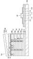
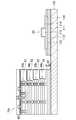
- FIG. 17is a plan view illustrating a manufacturing process of an intermediate substrate used in a manufacturing process of a semiconductor device according to an embodiment of the present invention.
- 18is a cross-sectional view taken along line XVIII-XVIII in FIG.
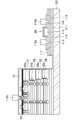
- FIG. 19is a plan view for explaining an intermediate substrate manufacturing process subsequent to FIG. 20 is a cross-sectional view taken along line XX-XX in FIG.
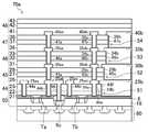
- FIG. 1 to 20show an embodiment of a semiconductor device and a manufacturing method thereof according to the present invention. Specifically, FIG. 1 is a cross-sectional view of the semiconductor device 130 of this embodiment.
- the semiconductor device 130includes a glass substrate 100 provided as a bonded substrate, a thin film element 80 formed on the glass substrate 100, a semiconductor element 90 bonded on the glass substrate 100, A resin layer 120 provided so as to cover the thin film element 80 and the semiconductor element 90, and a thin film element 80 (a source electrode 118a described later) and a semiconductor element 90 (a connection electrode 118c described later) provided on the resin layer 120. And a second connection wiring 121b for connecting to a thin film element 80 (a drain electrode 118b described later).
- the thin film element 80includes a semiconductor layer 113 provided on a glass substrate 100 via a first base coat film 111 and a second base coat film 112, and a gate provided so as to cover the semiconductor layer 113.
- An insulating film 114, a gate electrode 115 provided on the gate insulating film 114, and a first interlayer insulating film 116 and a second interlayer insulating film 117a provided in order so as to cover the gate electrode 115are provided.
- the semiconductor layer 113includes a channel region (not shown) provided so as to overlap with the gate electrode 115, and a source region (not shown) and a drain provided on one outer side and the other outer side of the channel region, respectively.
- a region(not shown), and is formed of a polysilicon film. Note that in the semiconductor layer 113, an LDD (Lightly Doped Drain) region may be provided between the channel region and the source and drain regions. Then, on the second interlayer insulating film 117a, as shown in FIG. 1, through each contact hole formed in the laminated film of the gate insulating film 114, the first interlayer insulating film 116, and the second interlayer insulating film 117a. A source electrode 118a and a drain electrode 118b connected to the source region and the drain region of the semiconductor layer 113 are provided.
- LDDLightly Doped Drain
- the semiconductor element 90includes a semiconductor element body 50, a first foundation layer 51, a second foundation layer 52, a third foundation layer 53, which are sequentially stacked on the glass substrate 100 side of the semiconductor element body 50.
- a thin film elementincluding a fourth base layer 54 and a fifth insulating layer 48, such that end portions of the base layers 51, 52, 53 and 54 on the thin film element 80 side gradually protrude toward the glass substrate 100 side.
- the end on the 80 sideis provided in a staircase pattern.
- the thickness of each of the foundation layers 51, 52, 53, and 54is, for example, about 0.5 ⁇ m
- the ends of the lower foundation layers (52, 53, and 54)are connected to the upper foundation layers (51, 53, 54). For example, it protrudes by about 1 ⁇ m from the ends of 52 and 53).
- the semiconductor element body 50is provided in an N-type NMOS transistor Ta provided in the left region of the single crystal silicon film 21 and in the right region of the single crystal silicon film 21.
- the configuration of the semiconductor element body 50is difficult to describe in detail with reference to FIG. 1 which is relatively small, in the description of the semiconductor chip forming process of the manufacturing method of the semiconductor device 130 which will be described later, This will be described in detail with reference to the drawings.
- the first underlayer 51includes a first insulating layer 44 including a first interlayer insulating film 22 and a second interlayer insulating film 23, and a first circuit pattern 25 aa stacked on the first insulating layer 44. , 25ab, 25ac and 25ad.
- the first circuit pattern 25aais formed in the N-type high concentration impurity region of the single crystal silicon film 21 of the NMOS transistor Ta through the first contact hole 44a formed in the first insulating layer 44. Connected to one of the. Further, as shown in FIG.
- the first circuit pattern 25abis formed in the N-type high concentration impurity region of the single crystal silicon film 21 of the NMOS transistor Ta through the first contact hole 44b formed in the first insulating layer 44. In addition to being connected to the other, it is connected to the connection electrode 118c through the first contact hole 44c and the like formed in the first insulating layer 44 and the gate oxide film 8. Further, as shown in FIG. 1, the first circuit pattern 25ac is formed in the P-type high concentration impurity region of the single crystal silicon film 21 of the PMOS transistor Tb through the first contact hole 44d formed in the first insulating layer 44.
- the first circuit pattern 25adis connected to the other of the P-type high concentration impurity regions of the single crystal silicon film 21 of the PMOS transistor Tb through the first contact hole 44e formed in the first insulating layer 44. ing.
- the second underlayer 52is laminated on the second insulating layer 45, the second insulating layer 45 including the first planarizing film 26, the first interlayer insulating film 27, and the second interlayer insulating film 28.
- Second circuit patterns 30aa and 30abare connected to the first circuit pattern 25ab via the second contact hole 45a formed in the second insulating layer 45, and the second circuit pattern 30ab is It is connected to the first circuit pattern 25ad through a second contact hole 45b formed in the second insulating layer 45.
- the third underlayer 53is laminated on the third insulating layer 46, the third insulating layer 46 including the second planarizing film 31, the first interlayer insulating film 32, and the second interlayer insulating film 33.
- Third circuit patterns 35aa and 35abare connected to the second circuit pattern 30aa via the third contact hole 46a formed in the third insulating layer 46, and the third circuit pattern 35ab is The third circuit pattern 30ab is connected to the second circuit pattern 30ab through a third contact hole 46b formed in the third insulating layer 46.
- the fourth underlayer 54is laminated on the fourth insulating layer 47 and a fourth insulating layer 47 composed of the third planarizing film 36, the first interlayer insulating film 37, and the second interlayer insulating film 38.
- the fourth circuit patterns 40aa and 40abare provided.
- the fourth circuit pattern 40aais connected to the third circuit pattern 35aa through the fourth contact hole 47a formed in the fourth insulating layer 47
- the fourth circuit pattern 40abis The third circuit pattern 35ab is connected through a fourth contact hole 47b formed in the fourth insulating layer 47.
- the fifth insulating layer 48includes a fourth planarizing film 41, a first interlayer insulating film 42, and a second interlayer insulating film 43.
- the thin film element 80constitutes a switching element or a gate driver of each pixel whose minimum unit is an image
- the semiconductor element body 50constitutes a source driver, an IC of a controller, or the like
- a liquid crystal display deviceis configured.
- FIGS. 2 to 16are a series of explanatory views showing the manufacturing process of the semiconductor device 130 in cross section.
- FIG. 17is a plan view illustrating a manufacturing process of the intermediate substrate 60 used in the manufacturing process of the semiconductor device 130
- FIG. 18is a cross-sectional view taken along line XVIII-XVIII in FIG.
- FIG. 19is a plan view for explaining the manufacturing process of the intermediate substrate 60 subsequent to FIG. 17, and
- FIG. 20is a cross-sectional view taken along the line XX-XX in FIG.
- the manufacturing method of the present embodimentincludes a semiconductor chip forming process, a thin film element forming process, a bonding process, an etching process, and a connecting process.
- the thermal oxide film 2is for preventing contamination of the surface of the silicon substrate 1 in the subsequent ion implantation, and is not necessarily essential, and can be omitted.
- N-type impurity element Infor example, phosphorus
- the P-type impurity elementis implanted into the entire surface of the silicon substrate 1 in a later step, it is preferable to set the implantation amount of the N-type impurity element in consideration of the amount canceled by the P-type impurity element.
- a P-type impurity element Ip(for example, boron) is implanted into the entire surface of the silicon substrate 1 by, for example, an ion implantation method.
- the implantation energyis about 10 keV to 50 keV and the dose is about 1 ⁇ 10 12 cm ⁇ 2 to 1 ⁇ 10 13 cm ⁇ 2 .
- phosphorussince phosphorus has a smaller diffusion coefficient in silicon with respect to heat treatment than boron, phosphorus may be appropriately diffused in advance in the silicon substrate by performing heat treatment before injecting the boron element.
- a P-type impurity elementmay be implanted after forming a resist on the N-well formation region. In this case, it is not necessary to consider cancellation due to P-type impurities during N-type impurity implantation in the N well formation region.
- a thermal oxide film 4 having a thickness of about 30 nmis formed by performing a heat treatment at about 900 ° C. to 1000 ° C. in an oxidizing atmosphere. At the same time, the impurity element is diffused to form the N well region 5 and the P well region 6.
- a silicon nitride film having a thickness of about 200 nmis formed on the entire substrate on which the N well region 5 and the P well region 6 are formed by, for example, CVD (Chemical Vapor Deposition) method, and then the silicon nitride film Then, the thermal oxide film 4 underneath is patterned using photolithography or the like to form a silicon nitride film 16a and a thermal oxide film 4a as shown in FIG.
- CVDChemical Vapor Deposition
- LOCOSLOCal Oxidation of Silicon
- a silicon nitride film 16bis formed.
- the LOCOS oxide film 7is for element isolation.
- element isolationmay be performed by, for example, STI (Shallow Trench Isolation).
- a heat treatment at about 1000 ° C.is performed in an oxygen atmosphere, so that the gate oxidation of about 10 nm to 20 nm is performed by the LOCOS oxide film 7 as shown in FIG. A film 8 is formed.
- an N-type impurity or a P-type impuritymay be implanted into the region where the NMOS transistor Ta or the PMOS transistor Tb is formed by ion implantation in order to control the threshold voltage of the transistor. Good.
- a polysilicon film having a thickness of about 300 nmis deposited on the entire substrate on which the gate oxide film 8 is formed, for example, by the CVD method, and then the polysilicon film is deposited. Is patterned using photolithography or the like to form the gate electrode 9a of the NMOS transistor Ta, the gate electrode 9b of the PMOS transistor Tb, and the relay electrode 9c.
- the gate electrode 9ais used as a mask by ion implantation, for example.
- An N-type low concentration impurity region 11is formed by implanting an N-type impurity element In (for example, phosphorus).
- the doseis preferably about 5 ⁇ 10 12 cm ⁇ 2 to 5 ⁇ 10 13 cm ⁇ 2 .
- the impurity concentration of the N-type low concentration impurity region 11is, for example, 1 ⁇ 10 17 / cm 3 to 5 ⁇ 10 17 / cm 3 .
- oblique implantation (HALO implantation) of a P-type impurity element such as boronmay be performed.
- the P typeBy implanting an impurity element Ip (for example, boron), a P-type low concentration impurity region 13 is formed.
- the doseis preferably about 5 ⁇ 10 12 cm ⁇ 2 to 5 ⁇ 10 13 cm ⁇ 2 .
- the impurity concentration of the P-type low-concentration impurity region 13is, for example, 1 ⁇ 10 17 / cm 3 to 5 ⁇ 10 17 / cm 3 .
- oblique implantationof an N-type impurity element such as phosphorus may be performed. Since boron has a large thermal diffusion coefficient, if a low-concentration impurity region of PMOS can be formed only by thermal diffusion of boron implanted by P-type high-concentration impurity implantation into the PMOS transistor in a later process, it is not always necessary. Impurity implantation for forming the P-type low concentration impurity region may not be performed.
- the resist 12is removed, and a silicon oxide film is formed by, for example, a CVD method, and then anisotropic dry etching is performed on the silicon oxide film.
- Side walls 14a, 14b and 14care formed on the side walls of the gate electrodes 9a and 9b and the relay electrode 9c, respectively.
- a resist 15is formed so that the NMOS transistor formation region is opened, and the N-type impurity element In is formed by, for example, ion implantation using the gate electrode 9a and the side wall 14a as a mask.
- the N-type high concentration impurity region 11ais formed.
- the impurity concentration of the N-type high concentration impurity region 11ais, for example, 1 ⁇ 10 19 / cm 3 to 1 ⁇ 10 21 / cm 3 .
- a P-type high-concentration impurity region 13ais formed by implanting a P-type impurity element Ip (for example, boron).
- Ipfor example, boron
- the impurity concentration of the P-type high concentration impurity region 13ais, for example, 1 ⁇ 10 19 / cm 3 to 5 ⁇ 10 20 / cm 3 .
- the implanted impurity elementis activated to form the NMOS transistor Ta and the PMOS transistor Tb.
- an insulating filmsuch as a silicon oxide film is formed on the entire substrate on which the NMOS transistor Ta and the PMOS transistor Tb are formed, and CMP (Chemical-Mechanical-Polishing) is performed on the insulating film.
- CMPChemical-Mechanical-Polishing
- a stripping substance Ih containing at least one of inert elements such as hydrogen, He or Neis implanted into the silicon substrate 1 by, for example, an ion implantation method.
- the release layer 19is formed, and the semiconductor substrate 20 is formed.
- the injection condition of the peeling materialfor example, when hydrogen is used, the dose is set to 2 ⁇ 10 16 cm ⁇ 2 to 2 ⁇ 10 17 cm ⁇ 2 and the injection energy is set to about 100 keV to 200 keV.
- the surface to be bonded of the semiconductor substrate 20 on which the release layer 19 is formed and the surface to be bonded of the intermediate substrate 60are subjected to a hydrophilic treatment by ammonia-hydrogen peroxide SC1 cleaning, and then the semiconductor substrate 20.
- a hydrophilic treatment by ammonia-hydrogen peroxide SC1 cleaningAs shown in FIG. 6C, the surface to be bonded and the surface to be bonded of the intermediate substrate 60 are superposed and heat-treated at 200 ° C. to 300 ° C. for about 2 hours, for example.
- the substrate 60is bonded.
- the intermediate substrate 60is provided in a thermal oxide layer 62 in which a plurality of openings 62 a are formed in a matrix, and a layer below the thermal oxide layer 62.
- the intermediate substrate 60includes the above-described thermal oxide layer 62 and columnar silicon structures 64 that support the thermal oxide layer 62 at a plurality of locations.
- a separation structure 65 that is separable from 62is provided.
- the intermediate substrate 60is formed by first thermally oxidizing the silicon substrate 61a to form a thermal oxide film having a thickness of about 100 to 300 nm, and then patterning the thermal oxide film using photolithography or the like. As shown in FIGS.
- a thermal oxide layer 62having a plurality of openings 62a each having an opening in a square shape having a side of about 0.5 ⁇ m and an opening pitch of about 1.5 ⁇ m is formed.
- the upper layer portion of the silicon substrate 61ais etched by a gas such as xenon difluoride through each opening 62a to form a concave portion 63a as shown in FIGS. Can do.
- a gassuch as xenon difluoride
- an alkaline solutionsuch as TMAH (TetraMethyloxideAmmonium Hydroxide) may be used.
- TMAHTetraMethyloxideAmmonium Hydroxide
- the temperature of the semiconductor substrate 20 and the intermediate substrate 60 bonded to each otheris increased to about 550 ° C. to 600 ° C., so that the silicon substrate 1 is moved along the release layer 19 to the silicon substrate as shown in FIG.
- the NMOS transistor Ta and the PMOS transistor Tbare temporarily transferred onto the intermediate substrate 60 after being separated into 1a and 1b.
- the silicon substrate 1bis polished or etched until the gate oxide film 8 is exposed, A single crystal silicon film 21 is formed and element isolation is performed.
- a first interlayer insulating film 22such as a silicon oxide film is formed to a thickness of about 100 nm, and then 650 ° C. to 800 ° C.
- the thickness of the second interlayer insulating film 23such as a silicon oxide film is increased in order to improve the reproducibility of characteristics and stabilize the transistor characteristics, and to maintain sufficient inter-wiring capacitance without affecting the transistor characteristics. It is formed to about 700 nm.
- the heat treatment temperatureis preferably 850 ° C. or lower so that the impurity profile of the transistor is not disturbed.
- the source region and the drain region of the NMOS transistor Taare obtained by partially etching the single crystal silicon film 21, the first interlayer insulating film 22, and the second interlayer insulating film 23.
- a first opening 44f exposing the end of the P-type high concentration impurity region 13 of the PMOS transistor Tbis formed, and the gate oxide film 8, the first interlayer insulating film 22, and the second interlayer insulating film 23 are partially formed.
- the first contact hole 44c reaching the relay electrode 9cis formed by etching.
- the metal filmis patterned using photolithography or the like, thereby forming the figure.
- the first circuit patterns 25aa to 25ad and the first metal layer 25bare formed.
- a titanium film and a titanium nitride film to be the barrier metal layers 24a and 24bare sequentially formed, and then Al— is used as a low resistance metal film. It is formed by forming a Cu alloy film or the like and patterning the laminated film.
- the impurity concentration of the N-type high concentration impurity region 11a and the P-type high concentration impurity region 13ais 1 ⁇ 10 19 / cm 3 to 1 ⁇ 10 21 / cm 3 and 1 ⁇ 10 19 / cm 3 to 1 ⁇ 10 20. Since / cm 3 , the first circuit patterns 25aa to 25ad and the single crystal silicon film 21 can be reliably connected to a low resistance. Further, when forming the first contact holes 44a, 44b, 44d and 44d, after exposing the silicon surface under an etching condition with a high selectivity between the oxide film and the silicon film, the silicon film up to the high concentration impurity region is formed.
- the single crystal silicon filmis preferably etched in consideration of the thickness.
- a metalsuch as Al—Si, Al—Cu, or Cu is used. Even if the material is used as a circuit pattern, diffusion of the metal material can be suppressed.
- a silicon oxide filmwas formed on the entire substrate on which the first circuit patterns 25aa to 25ad and the first metal layer 25b were formed using a mixed gas of TEOS (Tetraethoxysilane) and oxygen by PE (Plasma Enhanced) CVD or the like. Thereafter, the silicon oxide film is planarized by CMP or the like, thereby forming a first planarizing film 26 as shown in FIG.
- the first interlayer insulating filmas shown in FIG. 27, second interlayer insulating film 28, second contact holes 45a and 45b, second opening 45c, barrier metal layers 29a and 29b, second circuit patterns 30aa and 30ab, second metal layer 30b, second planarizing film 31 , First interlayer insulating film 32, second interlayer insulating film 33, third contact holes 46a and 46b, third opening 46c, barrier metal layers 34a and 34b, third circuit patterns 35aa and 35ab, third metal layer 35b, Third planarizing film 36, first interlayer insulating film 37, second interlayer insulating film 38, fourth contact holes 47a and 47b, fourth opening 47c, barrier metal After the 39a and 39b, the fourth circuit patterns 40aa and 40ab, the fourth metal layer 40b, the fourth planarization film 41, the first interlayer
- the semiconductor element body 50As described above, on the intermediate substrate 60, the semiconductor element body 50, the first base layer 51 provided with the first metal layer 25b at the outer end portion, and the second base layer 51 provided with the second metal layer 30b at the outer end portion.
- the base layer 52, the third base layer 53 provided with the third metal layer 35b at the outer end, the fourth base layer 54 provided with the fourth metal layer 40b at the outer end, and the fifth insulating layer 48are sequentially formed.
- a stacked semiconductor chip 70acan be formed.
- ⁇ Thin film element formation process(see FIG. 10 etc.)> First, after a silicon oxide film (thickness of about 100 nm) and a silicon nitride film (thickness of about 100 nm) are sequentially formed on the entire substrate on the glass substrate 100 by PECVD or the like, the silicon oxide film and the silicon nitride film are stacked.
- the first base coat film 111 and the second base coat film 112are formed by patterning the film using photolithography or the like.
- an amorphous silicon film(thickness of about 50 nm) is formed by PECVD or the like on the entire substrate on which the first base coat film 111 and the second base coat film 112 are formed, and the amorphous silicon film is converted into a polysilicon film by heat treatment. Then, the polysilicon film is patterned using photolithography or the like to form the semiconductor layer 113.
- a silicon oxide film(thickness of about 100 nm) is formed on the entire substrate on which the semiconductor layer 113 is formed by PECVD or the like, the silicon oxide film is patterned using photolithography or the like to obtain gate insulation. A film 114 is formed.
- a tantalum nitride film(thickness of about 50 nm) and a tungsten film (thickness of about 350 nm) are sequentially formed on the entire substrate on which the gate insulating film 114 is formed by sputtering, and then the tantalum nitride film and the tungsten film are formed.
- the gate electrode 115is formed.
- a channel regionoverlaps with the gate electrode 115 and the outside thereof.
- a heat treatmentis performed, and an activation treatment of the implanted phosphorus is performed, whereby an N-channel TFT is formed.
- a method of forming an N-channel TFT by injecting phosphorusis exemplified, but, for example, boron may be injected to form a P-channel TFT.
- a silicon oxide film(thickness of about 50 nm) is formed on the entire substrate on which the gate electrode 115 is formed by PECVD or the like, the silicon oxide film is patterned using photolithography or the like. A one-layer insulating film 116 is formed.
- the thin film element 80can be formed as described above.
- an ammonia-hydrogen peroxide systemis applied to the bonded surface of the semiconductor chip 70a formed in the semiconductor chip forming step and the bonded surface of the glass substrate 100 on which the thin film element 80 is formed in the thin film element forming step.
- the glass substrate on which the thin film element 80 is formed as shown in FIG. 10is obtained by superposing the surface to be bonded of the semiconductor chip 70a and the surface to be bonded of the glass substrate 100 after performing the hydrophilic treatment by SC1 cleaning.
- a semiconductor chip 70 ais bonded onto 100.
- the average surface roughness Ra of the surface to be bondedsatisfies the condition of 0.2 nm to 0.3 nm or less.
- the surface to be bonded of the semiconductor chip 70a and the surface to be bonded of the glass substrate 100are bonded by van der Waals force and hydrogen bond, and then heat-treated at about 400 ° C. to 600 ° C.
- -Si-OHsurface to be bonded of glass substrate 100
- -Si-OHsurface to be bonded of semiconductor chip 70a (second interlayer insulating film 43)
- -Si-O-Si- + H 2 OIt is changed to a strong bond between atoms by the reaction of.
- the glass substrateis exemplified as the bonded substrate.
- a metal substratesuch as stainless steel whose surface is covered with an insulating material (silicon oxide film, silicon nitride film, etc.) is used. It may be used.
- substrateis excellent in impact resistance, for example in an organic EL (Electro Luminescence) display apparatus etc., since the transparency of a board
- itmay be a plastic substrate whose surface is covered with a silicon oxide film. Such a form is suitable for a lighter display device. In this case, the intermediate substrate and the plastic substrate may be bonded together with an adhesive or the like.
- the gate insulating film 114 and the first interlayer Contact holeswere respectively formed in the laminated film of the insulating film 116 and the second interlayer insulating film 117, and the laminated film of the planarizing film 18 and the second interlayer insulating film 117, and then a metal film such as an aluminum film was formed. After that, the metal film is patterned using photolithography or the like to form the source electrode 118a, the drain electrode 118b, and the connection electrode 118c.
- a resist 119is formed on the glass substrate 100 on which the source electrode 118a, the drain electrode 118b, and the connection electrode 118c are formed in the bonding step.
- the insulating film such as the second interlayer insulating film 117 and the planarizing film 18 exposed from the resist 119is removed by wet etching, and subsequently, the metal layers 25b, 30b, 35b and 40b, and the barrier metal layers 24b, 29b, Metal films such as 34b and 39b are removed by wet etching using an etchant different from the etchant used for wet etching of the insulating film, and as shown in FIG.
- the semiconductor element 90is formed by processing the end of the semiconductor chip 70b on the thin film element 80 side in a stepped manner so that the part gradually protrudes toward the glass substrate 100 side.
- ⁇ Connection process>First, the resist 119 used in the etching process is removed, and then a photosensitive resin film is formed so as to cover the thin film element 80 and the semiconductor element 90, and then the photosensitive resin film is exposed and developed. Thus, as shown in FIG. 16, a resin layer 120 that covers at least the end of the semiconductor element 90 on the thin film element 80 side is formed.
- the transparent insulating filmis patterned using photolithography or the like. As shown in FIG. 1, the first connection wiring 121 a and the second connection wiring 121 b are formed to connect the thin film element 80 and the semiconductor element body 50.
- the semiconductor device 130can be manufactured as described above.
- the metal layer at the outer end portion of each of the foundation layers 51 to 54 in the semiconductor chip 70b bonded to the glass substrate 100 in the etching processBy etching 25b, 30b, 35b, and 40b, the end portions on the thin film element 80 side of each of the underlayers 51 to 54 stacked on the glass substrate 100 side of the semiconductor element body 50 gradually protrude toward the glass substrate 100 side.
- the semiconductor element 90is formed by processing the end of the semiconductor chip 70b bonded on the glass substrate 100 on the thin film element 80 side stepwise, the semiconductor element having the multilayer film structure with the thin film element 80 is formed.
- a TFTis exemplified as the thin film element 80, but it may be a TFD (Thin Film Diode) or the like.
- the present inventioncan be reliably connected to a thin film element and a semiconductor element having a multilayer wiring structure, and thus is useful for a display device such as a liquid crystal display device or an organic EL display device.
Landscapes
- Engineering & Computer Science (AREA)
- Physics & Mathematics (AREA)
- Condensed Matter Physics & Semiconductors (AREA)
- General Physics & Mathematics (AREA)
- Manufacturing & Machinery (AREA)
- Computer Hardware Design (AREA)
- Microelectronics & Electronic Packaging (AREA)
- Power Engineering (AREA)
- Thin Film Transistor (AREA)
- Internal Circuitry In Semiconductor Integrated Circuit Devices (AREA)
- Metal-Oxide And Bipolar Metal-Oxide Semiconductor Integrated Circuits (AREA)
Abstract
Description
Translated fromJapanese本発明は、半導体装置及びその製造方法に関し、特に、薄膜素子が形成された基板に半導体素子が接合された半導体装置及びその製造方法に関するものである。The present invention relates to a semiconductor device and a manufacturing method thereof, and more particularly, to a semiconductor device in which a semiconductor element is bonded to a substrate on which a thin film element is formed and a manufacturing method thereof.
アクティブマトリクス駆動方式の液晶表示装置は、例えば、画像の最小単位である各画素毎にスイッチング素子として設けられた薄膜トランジスタ(Thin Film Transistor、以下、「TFT」とも称する)等の薄膜素子と、各画素のTFTを駆動するための駆動回路等の半導体素子とを備えている。An active matrix liquid crystal display device includes, for example, a thin film element such as a thin film transistor (hereinafter also referred to as “TFT”) provided as a switching element for each pixel which is a minimum unit of an image, and each pixel. And a semiconductor element such as a drive circuit for driving the TFT.
近年、液晶表示装置では、例えば、連続粒界結晶シリコン(Continuous Grain Silicon)を用いて、駆動回路等の周辺回路がモノリシックに形成されたシステム液晶が注目されている。このシステム液晶では、低消費電力化や高精細化等を図るために、周辺回路にサブミクロンオーダーのデザインルール、すなわち、IC(Integrated Circuit)レベルの微細なパターン精度が求められているものの、使用するガラス基板に対応するステッパ等の製造技術がないので、サブミクロンオーダーの高性能な半導体素子をガラス基板上に直接形成することが困難である。そこで、シリコン基板を用いて高性能な半導体素子を形成した後に、その形成された半導体素子のチップをガラス基板上に転写により接合して、高性能な半導体素子をガラス基板上に形成する方法が提案されている。Recently, in a liquid crystal display device, for example, a system liquid crystal in which peripheral circuits such as a drive circuit are monolithically formed using continuous grain boundary crystal silicon (Continuous Grain Silicon) has attracted attention. In this system liquid crystal, the design rule of the submicron order, that is, IC (Integrated の Circuit) level fine pattern accuracy is required for the peripheral circuit in order to achieve low power consumption and high definition. Since there is no manufacturing technique such as a stepper corresponding to the glass substrate to be manufactured, it is difficult to directly form a high-performance semiconductor element of submicron order on the glass substrate. Therefore, there is a method of forming a high-performance semiconductor element on a glass substrate by forming a high-performance semiconductor element using a silicon substrate and then joining the formed semiconductor element chip onto the glass substrate by transfer. Proposed.
例えば、特許文献1には、シリコン層及び金属層が積層された構造を有する半導体素子を基板上に転写し、加熱により、シリコン層中の金属層側の部分を構成するシリコンと、金属層中のシリコン層側の部分を構成する金属とから金属シリサイドを形成する、半導体装置の製造方法が開示されている。For example,
ところで、TFT等の薄膜素子が形成されたガラス基板にICチップ等の半導体素子が転写された従来の半導体装置では、半導体素子に一体に形成された回路パターンの占有面積を抑制して、回路パターンの電気抵抗を低くするために、半導体素子において、複数の回路パターンを絶縁膜を介して互いに重なるように形成し、各層の回路パターンを絶縁膜のコンタクトホールを介して互いに接続する多層配線構造を取ることが多い。ここで、半導体素子は、シリコン基板をダイシングして形成されるので、半導体素子の各側壁は、被接合基板であるガラス基板の表面に対して直立している。そのため、ガラス基板に形成された薄膜素子と、そのガラス基板に接合された多層配線構造を有する半導体素子との間には、大きな段差ができてしまう。そして、ガラス基板上の薄膜素子及び半導体素子を樹脂層で覆って、その樹脂層上に接続配線を形成して、その接続配線を介して薄膜素子と半導体素子とを接続する場合には、薄膜素子と多層配線構造を有する半導体素子との間に形成された大きな段差により、接続配線が断線するおそれがある。By the way, in a conventional semiconductor device in which a semiconductor element such as an IC chip is transferred to a glass substrate on which a thin film element such as a TFT is formed, the area occupied by the circuit pattern formed integrally with the semiconductor element is suppressed and the circuit pattern is reduced. In order to reduce the electrical resistance of the semiconductor device, a multilayer wiring structure in which a plurality of circuit patterns are formed so as to overlap each other through an insulating film in a semiconductor element, and the circuit patterns of each layer are connected to each other through a contact hole of the insulating film. I often take it. Here, since the semiconductor element is formed by dicing a silicon substrate, each side wall of the semiconductor element is upright with respect to the surface of the glass substrate which is a bonded substrate. Therefore, a large step is formed between the thin film element formed on the glass substrate and the semiconductor element having a multilayer wiring structure bonded to the glass substrate. When the thin film element and the semiconductor element on the glass substrate are covered with a resin layer, a connection wiring is formed on the resin layer, and the thin film element and the semiconductor element are connected via the connection wiring, the thin film element There is a possibility that the connection wiring is disconnected due to a large step formed between the element and the semiconductor element having a multilayer wiring structure.
本発明は、かかる点に鑑みてなされたものであり、その目的とするところは、被接合基板上に設けられた薄膜素子と多層配線構造を有する半導体素子とを確実に接続することにある。The present invention has been made in view of such a point, and an object of the present invention is to reliably connect a thin film element provided on a bonded substrate and a semiconductor element having a multilayer wiring structure.
上記目的を達成するために、本発明は、半導体素子の薄膜素子側の端部が階段状に設けられていると共に樹脂層で被覆され、薄膜素子及び半導体素子本体が樹脂層上に設けられた接続配線を介して互いに接続されるようにしたものである。In order to achieve the above object, according to the present invention, the end of the semiconductor element on the thin film element side is provided in a staircase shape and covered with a resin layer, and the thin film element and the semiconductor element body are provided on the resin layer. They are connected to each other via connection wiring.
具体的に本発明に係る半導体装置は、被接合基板と、上記被接合基板上に形成された薄膜素子と、上記被接合基板上に接合され、各々、絶縁層及び該絶縁層に積層された回路パターンを有し、該各回路パターンが該各絶縁層に形成されたコンタクトホールを介して互いに接続された複数の下地層が半導体素子本体の上記被接合基板側に積層された半導体素子とを備えた半導体装置であって、上記半導体素子の上記薄膜素子側の端部は、上記各下地層の上記薄膜素子側の端部が上記被接合基板側に行くに従って次第に突出するように、階段状に設けられていると共に、樹脂層で被覆され、上記薄膜素子と上記半導体素子本体とは、上記樹脂層上に設けられた接続配線を介して互いに接続されていることを特徴とする。Specifically, a semiconductor device according to the present invention is bonded to a bonded substrate, a thin film element formed on the bonded substrate, and the bonded substrate, and is laminated on the insulating layer and the insulating layer, respectively. A semiconductor element having a circuit pattern, and a plurality of base layers connected to each other through contact holes formed in the respective insulating layers and laminated on the bonded substrate side of the semiconductor element body; An end of the semiconductor element on the side of the thin film element is stepped so that the end of the base layer on the side of the thin film element gradually protrudes toward the bonded substrate side. The thin film element and the semiconductor element body are connected to each other through a connection wiring provided on the resin layer.
上記の構成によれば、半導体素子本体の被接合基板側に積層された各下地層の薄膜素子側の端部が被接合基板側に行くに従って次第に突出するように、被接合基板上に接合された半導体素子の薄膜素子側の端部が階段状に設けられているので、薄膜素子と多層配線構造を有する半導体素子との間に大きな段差があるものの、例えば、半導体素子の各側壁が被接合基板に対して直立している場合よりも、半導体素子の薄膜素子側の側壁の全体的な傾斜が緩くなる。そして、その半導体素子の薄膜素子側の全体的な傾斜が緩くなった側壁、すなわち、半導体素子の薄膜素子側の端部が樹脂層で被覆されているので、例えば、半導体素子の各側壁が被接合基板に対して直立している場合よりも、樹脂層の表面が平坦になる。これにより、薄膜素子と多層配線構造を有する半導体素子との間に大きな段差があっても、樹脂層上に設けられた接続配線が断線し難くなるので、薄膜素子及び半導体素子本体が接続配線を介して確実に接続されることになり、被接合基板上に設けられた薄膜素子と多層配線構造を有する半導体素子とが確実に接続される。According to said structure, it joins on a to-be-joined board | substrate so that the edge part by the side of the thin film element of each base layer laminated | stacked on the to-be-joined board | substrate side of a semiconductor element body may protrude gradually as it goes to the to-be-joined substrate side. Since the end of the semiconductor element on the thin film element side is provided in a stepped shape, there is a large step between the thin film element and the semiconductor element having a multilayer wiring structure. The overall inclination of the side wall on the thin film element side of the semiconductor element becomes gentler than in the case of standing upright with respect to the substrate. Then, the side wall of the semiconductor element on the thin film element side that has become looser, that is, the end of the semiconductor element on the thin film element side is covered with the resin layer, so that, for example, each side wall of the semiconductor element is covered. The surface of the resin layer becomes flatter than the case where it stands upright with respect to the bonding substrate. As a result, even if there is a large step between the thin film element and the semiconductor element having a multilayer wiring structure, the connection wiring provided on the resin layer is difficult to be disconnected. Thus, the thin film element provided on the substrate to be bonded and the semiconductor element having a multilayer wiring structure are reliably connected.
上記被接合基板は、ガラス基板であってもよい。The substrate to be bonded may be a glass substrate.
上記の構成によれば、被接合基板がガラス基板であるので、例えば、液晶表示装置を構成するガラス製のアクティブマトリクス基板において、半導体装置が具体的に構成される。According to the above configuration, since the bonded substrate is a glass substrate, for example, a semiconductor device is specifically configured in a glass active matrix substrate that constitutes a liquid crystal display device.
上記薄膜素子は、薄膜トランジスタであり、上記半導体素子本体は、MOSトランジスタであってもよい。The thin film element may be a thin film transistor, and the semiconductor element body may be a MOS transistor.
上記の構成によれば、薄膜素子が薄膜トランジスタであり、半導体素子本体がMOS(Metal Oxide Semiconductor)トランジスタであるので、例えば、液晶表示装置を構成するガラス製のアクティブマトリクス基板において、薄膜素子により各画素のスイッチング素子やゲートドライバ等が具体的に構成され、半導体素子本体によりソースドライバやコントローラーのIC等が具体的に構成される。According to the above configuration, since the thin film element is a thin film transistor and the semiconductor element body is a MOS (Metal Oxide Semiconductor) transistor, for example, in a glass active matrix substrate constituting a liquid crystal display device, each pixel is formed by a thin film element. The switching element, gate driver, and the like are specifically configured, and the semiconductor element body specifically configures a source driver, a controller IC, and the like.
また、本発明に係る半導体装置の製造方法は、半導体素子本体を形成した後に、各々、絶縁層及び該絶縁層に積層された回路パターンを有し、該各回路パターンが該各絶縁層に形成されたコンタクトホールを介して互いに接続された複数の下地層を形成する際に、該各下地層の外端部に上記各回路パターンと同一層に同一材料により金属層を所定の大きさに形成することにより、半導体チップを形成する半導体チップ形成工程と、被接合基板上に薄膜素子を形成する薄膜素子形成工程と、上記薄膜素子が形成された被接合基板上に上記半導体チップを上記半導体素子本体側が上方になるように接合する接合工程と、上記被接合基板上に接合された半導体チップにおける上記各下地層の外端部の金属層をエッチングすることにより、上記各下地層の上記薄膜素子側の端部が上記被接合基板側に行くに従って次第に突出するように、上記半導体チップの上記薄膜素子側の端部を階段状に加工して、半導体素子を形成するエッチング工程と、上記半導体素子の上記薄膜素子側の端部を樹脂層で被覆した後に、該樹脂層上に接続配線を形成して、上記薄膜素子と上記半導体素子本体とを互いに接続する接続工程とを備えることを特徴とする。In addition, the method for manufacturing a semiconductor device according to the present invention includes an insulating layer and a circuit pattern laminated on the insulating layer after the semiconductor element body is formed, and the circuit patterns are formed on the insulating layers. When forming a plurality of base layers connected to each other through the formed contact holes, a metal layer is formed in a predetermined size on the outer edge of each base layer with the same material as the circuit pattern. A semiconductor chip forming step of forming a semiconductor chip; a thin film element forming step of forming a thin film element on a bonded substrate; and the semiconductor chip on the bonded substrate on which the thin film element is formed. The bonding step for bonding the main body side upward, and etching the metal layer at the outer end of each base layer in the semiconductor chip bonded on the substrate to be bonded, Etching process for forming a semiconductor element by processing the end part on the thin film element side of the semiconductor chip in a stepped manner so that the end part on the thin film element side of the layer gradually protrudes toward the bonded substrate side And connecting the thin film element and the semiconductor element main body to each other by forming a connection wiring on the resin layer after covering the end of the semiconductor element on the thin film element side with a resin layer. It is characterized by providing.
上記の方法によれば、エッチング工程において、被接合基板上に接合された半導体チップにおける各下地層の外端部の金属層をエッチングすることにより、半導体素子本体の被接合基板側に積層された各下地層の薄膜素子側の端部が被接合基板側に行くに従って次第に突出するように、被接合基板上に接合された半導体チップの薄膜素子側の端部を階段状に加工して、半導体素子を形成するので、薄膜素子と多層配線構造を有する半導体素子との間に大きな段差があるものの、例えば、半導体素子の各側壁が被接合基板に対して直立している場合よりも、半導体素子の薄膜素子側の側壁の全体的な傾斜が緩くなる。そして、接続工程において、その半導体素子の薄膜素子側の全体的な傾斜が緩くなった側壁、すなわち、半導体素子の薄膜素子側の端部を樹脂層で被覆するので、例えば、半導体素子の各側壁が被接合基板に対して直立している場合よりも、樹脂層の表面が平坦になる。これにより、薄膜素子と多層配線構造を有する半導体素子との間に大きな段差があっても、接続工程で樹脂層上に形成する接続配線が断線し難くなるので、薄膜素子及び半導体素子本体が接続配線を介して確実に接続されることになり、被接合基板上に設けられた薄膜素子と多層配線構造を有する半導体素子とが確実に接続される。According to the above method, in the etching step, the metal layer at the outer end portion of each base layer in the semiconductor chip bonded onto the bonded substrate is etched to be laminated on the bonded substrate side of the semiconductor element body. A semiconductor chip processed on the thin film element side of the semiconductor chip bonded on the bonded substrate is stepped so that the edge on the thin film element side of each underlying layer gradually protrudes toward the bonded substrate side. Since the element is formed, there is a large level difference between the thin film element and the semiconductor element having the multilayer wiring structure, but the semiconductor element is more than the case where each side wall of the semiconductor element is upright with respect to the bonded substrate, for example. The overall inclination of the side wall on the thin film element side becomes gentle. In the connecting step, the side wall of the thin film element side of the semiconductor element, which is loosened, that is, the end part of the semiconductor element on the thin film element side is covered with the resin layer. The surface of the resin layer becomes flatter than when the substrate is upright with respect to the bonded substrate. As a result, even if there is a large step between the thin film element and the semiconductor element having the multilayer wiring structure, the connection wiring formed on the resin layer in the connection process is difficult to be disconnected, so the thin film element and the semiconductor element body are connected. Thus, the thin film element provided on the bonded substrate and the semiconductor element having a multilayer wiring structure are reliably connected.
本発明によれば、半導体素子の薄膜素子側の端部が階段状に設けられていると共に樹脂層で被覆され、薄膜素子及び半導体素子本体が樹脂層上に設けられた接続配線を介して互いに接続されているので、被接合基板上に設けられた薄膜素子と多層配線構造を有する半導体素子とを確実に接続することができる。According to the present invention, the end of the semiconductor element on the thin film element side is provided in a stepped manner and covered with the resin layer, and the thin film element and the semiconductor element body are connected to each other via the connection wiring provided on the resin layer. Since they are connected, the thin film element provided on the bonded substrate and the semiconductor element having a multilayer wiring structure can be reliably connected.
以下、本発明の実施形態を図面に基づいて詳細に説明する。なお、本発明は、以下の実施形態に限定されるものではない。Hereinafter, embodiments of the present invention will be described in detail with reference to the drawings. In addition, this invention is not limited to the following embodiment.
図1~図20は、本発明に係る半導体装置及びその製造方法の一実施形態を示している。具体的に、図1は、本実施形態の半導体装置130の断面図である。1 to 20 show an embodiment of a semiconductor device and a manufacturing method thereof according to the present invention. Specifically, FIG. 1 is a cross-sectional view of the
半導体装置130は、図1に示すように、被接合基板として設けられたガラス基板100と、ガラス基板100上に形成された薄膜素子80と、ガラス基板100上に接合された半導体素子90と、薄膜素子80及び半導体素子90を覆うように設けられた樹脂層120と、樹脂層120上に設けられ、薄膜素子80(の後述するソース電極118a)及び半導体素子90(の後述する接続電極118c)を互いに接続するための第1接続配線121a、並びに薄膜素子80(の後述するドレイン電極118b)に接続するための第2接続配線121bとを備えている。As shown in FIG. 1, the
薄膜素子80は、図1に示すように、ガラス基板100上に第1ベースコート膜111及び第2ベースコート膜112を介して設けられた半導体層113と、半導体層113を覆うように設けられたゲート絶縁膜114と、ゲート絶縁膜114上に設けられたゲート電極115と、ゲート電極115を覆うように順に設けられた第1層間絶縁膜116及び第2層間絶縁膜117aとを備えている。ここで、半導体層113は、ゲート電極115に重なるように設けられたチャネル領域(不図示)と、そのチャネル領域の一方の外側及び他方の外側にそれぞれ設けられたソース領域(不図示)及びドレイン領域(不図示)とを備え、ポリシリコン膜により構成されている。なお、半導体層113において、チャネル領域とソース領域及びドレイン領域との間には、LDD(Lightly Doped Drain)領域が設けられていてもよい。そして、第2層間絶縁膜117a上には、図1に示すように、ゲート絶縁膜114、第1層間絶縁膜116及び第2層間絶縁膜117aの積層膜に形成された各コンタクトホールを介して半導体層113のソース領域及びドレイン領域にそれぞれ接続されたソース電極118a及びドレイン電極118bが設けられている。As shown in FIG. 1, the
半導体素子90は、図1に示すように、半導体素子本体50と、半導体素子本体50のガラス基板100側に順に積層された第1下地層51、第2下地層52、第3下地層53、第4下地層54及び第5絶縁層48とを備え、各下地層51、52、53及び54の薄膜素子80側の端部がガラス基板100側に行くに従って次第に突出するように、その薄膜素子80側の端部が階段状に設けられている。ここで、各下地層51、52、53及び54の厚さは、例えば、0.5μm程度であり、下層の下地層(52、53及び54)の端は、その上層の下地層(51、52及び53)の端よりも、例えば、1μm程度それぞれ突出している。As shown in FIG. 1, the
半導体素子本体50は、図1に示すように、単結晶シリコン膜21の図中左側の領域に設けられたN型のNMOSトランジスタTaと、単結晶シリコン膜21の図中右側の領域に設けられたP型のPMOSトランジスタTbと、NMOSトランジスタTa及びPMOSトランジスタTbを分離するためのゲート酸化膜8と、NMOSトランジスタTa及びPMOSトランジスタTbを覆うように設けられた平坦化膜18とを備えている。なお、半導体素子本体50の構成については、相対的に小さく図示された図1を用いて詳細に説明し難いので、後述する半導体装置130の製造方法の半導体チップ形成工程の説明において、相対的に大きく図示された図面を用いて詳細に説明する。As shown in FIG. 1, the
第1下地層51は、図1に示すように、第1層間絶縁膜22及び第2層間絶縁膜23からなる第1絶縁層44と、第1絶縁層44に積層された第1回路パターン25aa、25ab、25ac及び25adとを備えている。ここで、第1回路パターン25aaは、図1に示すように、第1絶縁層44に形成された第1コンタクトホール44aを介してNMOSトランジスタTaの単結晶シリコン膜21のN型高濃度不純物領域の一方に接続されている。また、第1回路パターン25abは、図1に示すように、第1絶縁層44に形成された第1コンタクトホール44bを介してNMOSトランジスタTaの単結晶シリコン膜21のN型高濃度不純物領域の他方に接続されていると共に、第1絶縁層44及びゲート酸化膜8に形成された第1コンタクトホール44c等を介して、接続電極118cに接続されている。さらに、図1に示すように、第1回路パターン25acは、第1絶縁層44に形成された第1コンタクトホール44dを介してPMOSトランジスタTbの単結晶シリコン膜21のP型高濃度不純物領域の一方に接続され、第1回路パターン25adは、第1絶縁層44に形成された第1コンタクトホール44eを介してPMOSトランジスタTbの単結晶シリコン膜21のP型高濃度不純物領域の他方に接続されている。As shown in FIG. 1, the
第2下地層52は、図1に示すように、第1平坦化膜26、第1層間絶縁膜27及び第2層間絶縁膜28からなる第2絶縁層45と、第2絶縁層45に積層された第2回路パターン30aa及び30abとを備えている。ここで、図1に示すように、第2回路パターン30aaは、第2絶縁層45に形成された第2コンタクトホール45aを介して第1回路パターン25abに接続され、第2回路パターン30abは、第2絶縁層45に形成された第2コンタクトホール45bを介して第1回路パターン25adに接続されている。As shown in FIG. 1, the
第3下地層53は、図1に示すように、第2平坦化膜31、第1層間絶縁膜32及び第2層間絶縁膜33からなる第3絶縁層46と、第3絶縁層46に積層された第3回路パターン35aa及び35abとを備えている。ここで、図1に示すように、第3回路パターン35aaは、第3絶縁層46に形成された第3コンタクトホール46aを介して第2回路パターン30aaに接続され、第3回路パターン35abは、第3絶縁層46に形成された第3コンタクトホール46bを介して第2回路パターン30abに接続されている。As shown in FIG. 1, the
第4下地層54は、図1に示すように、第3平坦化膜36、第1層間絶縁膜37及び第2層間絶縁膜38からなる第4絶縁層47と、第4絶縁層47に積層された第4回路パターン40aa及び40abとを備えている。ここで、図1に示すように、第4回路パターン40aaは、第4絶縁層47に形成された第4コンタクトホール47aを介して第3回路パターン35aaに接続され、第4回路パターン40abは、第4絶縁層47に形成された第4コンタクトホール47bを介して第3回路パターン35abに接続されている。As shown in FIG. 1, the
第5絶縁層48は、図1に示すように、第4平坦化膜41、第1層間絶縁膜42及び第2層間絶縁膜43により構成されている。As shown in FIG. 1, the fifth insulating
上記構成の半導体装置130は、例えば、薄膜素子80が画像の最小単位である各画素のスイッチング素子やゲートドライバ等を構成すると共に、半導体素子本体50がソースドライバやコントローラーのIC等を構成することにより、液晶表示装置を構成するものである。In the
次に、本実施形態の半導体装置130の製造方法について、図2~図20を用いて一例を挙げて説明する。ここで、図2~図16は、半導体装置130の製造工程を断面で示す一連の説明図である。また、図17は、半導体装置130の製造工程で用いる中間基板60の製造工程を説明する平面図であり、図18は、図17中のXVIII-XVIII線に沿った断面図である。さらに、図19は、図17に続く中間基板60の製造工程を説明する平面図であり、図20は、図19中のXX-XX線に沿った断面図である。なお、本実施形態の製造方法は、半導体チップ形成工程、薄膜素子形成工程、接合工程、エッチング工程及び接続工程を備える。Next, a method for manufacturing the
<半導体チップ形成工程>
まず、図2(a)に示すように、シリコン基板(単結晶シリコン基板)1上に、例えば、30nm程度の熱酸化膜2を形成する。ここで、熱酸化膜2は、後のイオン注入において、シリコン基板1の表面の汚染を防ぐためのものであり、必ずしも必須でないので、省略することができる。<Semiconductor chip formation process>
First, as shown in FIG. 2A, a
続いて、図2(b)に示すように、熱酸化膜2上にレジスト3を形成した後に、レジスト3をマスクにして、レジスト3の開口領域であるNウェル形成領域に、例えば、イオン注入法により、N型不純物元素In(例えば、リン)を注入する。ここで、イオン注入の条件としては、注入エネルギーを50keV~150keV程度に設定すると共に、ドーズ量を1×1012cm-2~1×1013cm-2程度とすることが好ましい。また、後の工程において、P型不純物元素をシリコン基板1の全面に注入するので、このP型不純物元素によって打ち消される量を考慮して、N型不純物元素の注入量を設定することが好ましい。Subsequently, as shown in FIG. 2B, after forming a resist 3 on the
そして、図2(c)に示すように、レジスト3を除去した後、シリコン基板1全面に、例えば、イオン注入法により、P型不純物元素Ip(例えば、ボロン)を注入する。ここで、イオン注入の条件としては、注入エネルギーを10keV~50keV程度にすると共に、ドーズ量を1×1012cm-2~1×1013cm-2程度とすることが好ましい。また、リンは、ボロンに比べて熱処理に対するシリコン中の拡散係数が小さいので、ボロン元素を注入する前に熱処理を行い、予めリンをシリコン基板中に適度に拡散させてもよい。さらに、Nウェル形成領域においてP型不純物によるN型不純物の打ち消しを避けたい場合には、Nウェル形成領域上にレジストを形成した後に、P型不純物元素を注入してもよい。そして、この場合には、Nウェル形成領域でのN型不純物注入時におけるP型不純物による打ち消しを考慮する必要がない。Then, as shown in FIG. 2C, after removing the resist 3, a P-type impurity element Ip (for example, boron) is implanted into the entire surface of the
さらに、熱酸化膜2を除去した後に、図2(d)に示すように、酸化雰囲気中で900℃~1000℃程度の熱処理を行うことにより、厚さ30nm程度の熱酸化膜4を形成すると共に、不純物元素を拡散させて、Nウェル領域5及びPウェル領域6を形成する。Further, after removing the
引き続いて、Nウェル領域5及びPウェル領域6が形成された基板全体に、例えば、CVD(Chemical Vapor Deposition)法等により、厚さ200nm程度の窒化シリコン膜を成膜した後に、その窒化シリコン膜及びその下層の熱酸化膜4をフォトリソグラフィ等を用いてパターニングして、図3(a)に示すように、窒化シリコン膜16a及び熱酸化膜4aを形成する。Subsequently, a silicon nitride film having a thickness of about 200 nm is formed on the entire substrate on which the
その後、図3(b)に示すように、酸素雰囲気中で900℃~1000℃程度の熱処理によりLOCOS(LOCal Oxidation of Silicon)酸化を行うことにより、厚さ200nm~500nm程度のLOCOS酸化膜7及び窒化シリコン膜16bを形成する。ここで、LOCOS酸化膜7は、素子分離を行うためのものであるが、LOCOS酸化膜7の他に、例えば、STI(Shallow Trench Isolation)等で素子分離を行ってもよい。Thereafter, as shown in FIG. 3B, LOCOS (LOCal Oxidation of Silicon) oxidation is performed by heat treatment at about 900 ° C. to 1000 ° C. in an oxygen atmosphere. A
さらに、窒化シリコン膜16bを除去した後、酸素雰囲気中で1000℃程度の熱処理を行うことにより、図3(c)に示すように、LOCOS酸化膜7により、厚さ10nm~20nm程度のゲート酸化膜8を形成する。ここで、窒化シリコン膜16bを除去した後に、トランジスタの閾値電圧をコントロールするため、NMOSトランジスタTa又はPMOSトランジスタTbを形成する領域に、イオン注入法によってN型不純物又はP型不純物を注入してもよい。Further, after removing the
引き続いて、図4(a)に示すように、ゲート酸化膜8が形成された基板全体に、例えば、CVD法等により、厚さ300nm程度のポリシリコン膜を堆積させた後、そのポリシリコン膜をフォトリソグラフィ等を用いてパターニングして、NMOSトランジスタTaのゲート電極9a、PMOSトランジスタTbのゲート電極9b、及び中継電極9cを形成する。Subsequently, as shown in FIG. 4A, a polysilicon film having a thickness of about 300 nm is deposited on the entire substrate on which the
そして、LDD領域を形成するために、図4(b)に示すように、NMOSトランジスタ形成領域が開口するようにレジスト10を形成した後に、例えば、イオン注入法により、ゲート電極9aをマスクとして、N型不純物元素In(例えば、リン)を注入することにより、N型低濃度不純物領域11を形成する。ここで、イオン注入の条件としては、例えばドーズ量を5×1012cm-2~5×1013cm-2程度とすることが好ましい。このとき、N型低濃度不純物領域11の不純物濃度は、例えば、1×10¹⁷/cm3~5×1017/cm3となる。また、このとき、短チャネル効果を抑制するために、ボロン等のP型不純物元素の斜め注入(HALO注入)を行ってもよい。Then, in order to form the LDD region, as shown in FIG. 4B, after forming the resist 10 so as to open the NMOS transistor formation region, the
さらに、レジスト10を除去し、図4(c)に示すように、PMOSトランジスタ形成領域が開口するようにレジスト12を形成した後に、例えば、イオン注入法により、ゲート電極9bをマスクとして、P型不純物元素Ip(例えば、ボロン)を注入することにより、P型低濃度不純物領域13を形成する。ここで、イオン注入の条件としては、例えば、ドーズ量を5×1012cm-2~5×1013cm-2程度とすることが好ましい。このとき、P型低濃度不純物領域13の不純物濃度は、例えば、1×10¹⁷/cm3~5×1017/cm3となる。また、このとき、短チャネル効果を抑制するために、リン等のN型不純物元素の斜め注入(HALO注入)を行ってもよい。なお、ボロンは、熱拡散係数が大きいので、後工程でのPMOSトランジスタへのP型高濃度不純物注入により注入されたボロンの熱拡散のみでPMOSの低濃度不純物領域が形成できる場合には、必ずしもP型低濃度不純物領域を形成するための不純物注入を行わなくてもよい。Further, after removing the resist 10 and forming the resist 12 so as to open the PMOS transistor formation region as shown in FIG. 4C, for example, by ion implantation, using the
引き続いて、図5(a)に示すように、レジスト12を除去し、例えば、CVD法等により、酸化シリコン膜を形成した後に、その酸化シリコン膜に対して異方性ドライエッチングを行うことにより、ゲート電極9a及び9b並びに中継電極9cの各側壁にサイドウォール14a、14b及び14cをそれぞれ形成する。Subsequently, as shown in FIG. 5A, the resist 12 is removed, and a silicon oxide film is formed by, for example, a CVD method, and then anisotropic dry etching is performed on the silicon oxide film.
そして、図5(b)に示すように、NMOSトランジスタ形成領域が開口するようにレジスト15を形成し、例えば、イオン注入法により、ゲート電極9a及びサイドウォール14aをマスクとして、N型不純物元素In(例えば、リン)を注入することにより、N型高濃度不純物領域11aを形成する。ここで、N型高濃度不純物領域11aの不純物濃度は、例えば、1×10¹⁹/cm3~1×1021/cm3である。Then, as shown in FIG. 5B, a resist 15 is formed so that the NMOS transistor formation region is opened, and the N-type impurity element In is formed by, for example, ion implantation using the
さらに、レジスト15を除去し、図5(c)に示すように、PMOSトランジスタ形成領域が開口するようにレジスト17を形成した後に、例えば、イオン注入法により、ゲート電極9b及びサイドウォール14bをマスクとして、P型不純物元素Ip(例えば、ボロン)を注入することにより、P型高濃度不純物領域13aを形成する。ここで、P型高濃度不純物領域13aの不純物濃度は、例えば、1×10¹⁹/cm3~5×1020/cm3である。その後、例えば、900℃10分間の熱処理を行うことにより、注入した不純物元素の活性化を行って、NMOSトランジスタTa及びPMOSトランジスタTbを形成する。Further, after removing the resist 15 and forming the resist 17 so that the PMOS transistor formation region is opened as shown in FIG. 5C, the
引き続いて、レジスト17を除去した後に、NMOSトランジスタTa及びPMOSトランジスタTbが形成された基板全体に、酸化シリコン膜等の絶縁膜を成膜し、その絶縁膜に対して、CMP(Chemical Mechanical Polishing)等により平坦化を行うことにより、図6(a)に示すように、平坦化膜18を形成する。Subsequently, after removing the resist 17, an insulating film such as a silicon oxide film is formed on the entire substrate on which the NMOS transistor Ta and the PMOS transistor Tb are formed, and CMP (Chemical-Mechanical-Polishing) is performed on the insulating film. By performing planarization by, for example, the
そして、図6(b)で示すように、シリコン基板1に対して、例えば、イオン注入法により、水素、He又はNe等の不活性元素の少なくとも1つを含む剥離用物質Ihを注入することにより、剥離層19を形成して、半導体基板20を形成する。ここで、剥離用物質の注入条件としては、例えば、水素を用いる場合、ドーズ量を2×1016cm-2~2×1017cm-2とし、注入エネルギーを100keV~200keV程度とする。Then, as shown in FIG. 6B, a stripping substance Ih containing at least one of inert elements such as hydrogen, He or Ne is implanted into the
さらに、剥離層19が形成された半導体基板20の被接合表面、及び中間基板60の被接合表面に対して、アンモニア-過酸化水素系のSC1洗浄により親水化処理を行った後に、半導体基板20の被接合表面と中間基板60の被接合表面とを重ね合わせて、例えば、200℃~300℃で約2時間、熱処理することにより、図6(c)に示すように、半導体基板20及び中間基板60を接合する。ここで、中間基板60は、図6(c)、図19及び図20に示すように、複数の開口部62aがマトリクス状に形成された熱酸化層62と、熱酸化層62の下層に設けられ、熱酸化層62の各開口部62aにそれぞれ繋がる複数の凹状部63aが形成されたシリコン基板61bとを備えている。また、中間基板60には、図20に示すように、上述した熱酸化層62と、熱酸化層62を複数箇所で支持する柱状のシリコン構造64とにより構成され、シリコン基板61bと熱酸化層62とが分離可能な分離構造65が設けられている。そして、中間基板60は、まず、シリコン基板61aを熱酸化して、厚さ100~300nm程度の熱酸化膜を形成した後に、その熱酸化膜をフォトリソグラフィ等を用いてパターニングすることにより、図17及び図18に示すように、例えば、一辺が0.5μm程度の正方形状に開口し、その開口ピッチが1.5μm程度である複数の開口部62aを有する熱酸化層62を形成し、続いて、シリコン基板61aの上層部を各開口部62aを介して二フッ化キセノン等のガスによりエッチングして、図19及び図20に示すように、凹状部63aを形成することにより、製造することができる。なお、シリコン基板61aのエッチングには、TMAH(TetraMethyl Ammonium Hydroxide)等のアルカリ性溶液を用いてもよい。また、柱状のシリコン構造64の径及び高さを適切に設定することにより、後で行うCMP工程に耐え、且つ、ねじれ応力による分離が可能な中間基板60を設計することができる。Further, the surface to be bonded of the
引き続いて、互いに接合された半導体基板20及び中間基板60を550℃~600℃程度に昇温することにより、図7(a)に示すように、シリコン基板1を剥離層19に沿ってシリコン基板1a及び1bに分離して、中間基板60上にNMOSトランジスタTa及びPMOSトランジスタTbを一旦転写する。Subsequently, the temperature of the
そして、図7(b)に示すように、剥離層19を研磨(上述のCMP工程)又はエッチング等で除去した後に、ゲート酸化膜8が露出するまでシリコン基板1bを研磨又はエッチングすることにより、単結晶シリコン膜21を形成すると共に、素子分離を行う。Then, as shown in FIG. 7B, after removing the
その後、図7(c)に示すように、単結晶シリコン膜21の表面を保護するために、酸化シリコン膜等の第1層間絶縁膜22を厚さ100nm程度に形成した後に、650℃~800℃程度で30分~2時間程度、熱処理を行うことにより、単結晶シリコン膜21中の水素を除去すると共に、サーマルドナーや格子欠陥を完全に取り除き、且つ、P型不純物の再活性化、トランジスタ特性の再現性の向上、及びトランジスタ特性の安定化を図り、さらに、トランジスタ特性に影響を与えず、充分な配線間容量を保つために、酸化シリコン膜等の第2層間絶縁膜23を厚さ700nm程度に形成する。なお、熱処理の温度については、トランジスタの不純物プロファイルが乱れないように、850℃以下にすることが好ましい。Thereafter, as shown in FIG. 7C, in order to protect the surface of the single
引き続いて、図8(a)に示すように、単結晶シリコン膜21、第1層間絶縁膜22及び第2層間絶縁膜23を部分的にエッチングすることにより、NMOSトランジスタTaのソース領域及びドレイン領域を構成するN型高濃度不純物領域11aまで到達する第1コンタクトホール44a及び44b、PMOSトランジスタTbのソース領域及びドレイン領域を構成するP型高濃度不純物領域13aまで到達する第1コンタクトホール44d及び44e、並びにPMOSトランジスタTbのP型高濃度不純物領域13の端部が露出する第1開口部44fを形成すると共に、ゲート酸化膜8、第1層間絶縁膜22及び第2層間絶縁膜23を部分的にエッチングして、中継電極9cまで到達する第1コンタクトホール44cを形成する。Subsequently, as shown in FIG. 8A, the source region and the drain region of the NMOS transistor Ta are obtained by partially etching the single
そして、第1コンタクトホール44a~44e及び第1開口部44fが形成された基板全体に、低抵抗の金属膜を成膜した後に、その金属膜をフォトリソグラフィ等を用いてパターニングすることにより、図8(b)に示すように、第1回路パターン25aa~25ad及び第1金属層25bを形成する。ここで、第1回路パターン25aa~25ad及び第1金属層25bは、例えば、バリアメタル層24a及び24bとなるチタン膜及び窒化チタン膜等を順に成膜した後に、低抵抗の金属膜としてAl-Cu合金膜等を成膜して、それらの積層膜をパターニングすることにより形成される。また、N型高濃度不純物領域11a及びP型高濃度不純物領域13aの不純物濃度は、1×10¹⁹/cm3~1×1021/cm3及び1×1019/cm3~1×1020/cm3となっているので、各第1回路パターン25aa~25adと単結晶シリコン膜21とを確実に低抵抗に接続することができる。さらに、第1コンタクトホール44a、44b、44d及び44dを形成する際には、酸化膜とシリコン膜との選択比が高いエッチング条件でシリコン表面を露出させた後に、高濃度不純物領域までのシリコン膜厚を考慮して、単結晶シリコン膜をエッチングすることが好ましい。なお、本実施形態では、単結晶シリコン膜21中の水素を除去すると共に、サーマルドナーや格子欠陥を取り除くために、熱処理を既に行っているので、Al-Si、Al-Cu、Cu等の金属材料を回路パターンとして用いても、金属材料の拡散を抑制することができる。Then, after a low-resistance metal film is formed on the entire substrate on which the
さらに、第1回路パターン25aa~25ad及び第1金属層25bが形成された基板全体に、PE(Plasma Enhanced)CVD等によりTEOS(Tetraethoxysilane)及び酸素の混合ガスを用いて酸化シリコン膜を成膜した後に、その酸化シリコン膜に対して、CMP等により平坦化を行うことにより、図8(c)に示すように、第1平坦化膜26を形成する。Further, a silicon oxide film was formed on the entire substrate on which the first circuit patterns 25aa to 25ad and the
最後に、上述した第1層間絶縁膜、第2層間絶縁膜、コンタクトホール、回路パターン、金属層及び平坦化膜を形成する工程を繰り返すことにより、図9に示すように、第1層間絶縁膜27、第2層間絶縁膜28、第2コンタクトホール45a及び45b、第2開口部45c、バリアメタル層29a及び29b、第2回路パターン30aa及び30ab、第2金属層30b、第2平坦化膜31、第1層間絶縁膜32、第2層間絶縁膜33、第3コンタクトホール46a及び46b、第3開口部46c、バリアメタル層34a及び34b、第3回路パターン35aa及び35ab、第3金属層35b、第3平坦化膜36、第1層間絶縁膜37、第2層間絶縁膜38、第4コンタクトホール47a及び47b、第4開口部47c、バリアメタル層39a及び39b、第4回路パターン40aa及び40ab、第4金属層40b、第4平坦化膜41、第1層間絶縁膜42、並びに第2層間絶縁膜43を順に形成した後に、中間基板60を所定のサイズに分断する。Finally, by repeating the process of forming the first interlayer insulating film, the second interlayer insulating film, the contact hole, the circuit pattern, the metal layer, and the planarizing film, the first interlayer insulating film as shown in FIG. 27, second
以上のようにして、中間基板60に、半導体素子本体50、第1金属層25bが外端部に設けられた第1下地層51、第2金属層30bが外端部に設けられた第2下地層52、第3金属層35bが外端部に設けられた第3下地層53、第4金属層40bが外端部に設けられた第4下地層54、及び第5絶縁層48が順に積層された半導体チップ70aを形成することができる。As described above, on the
<薄膜素子形成工程(図10等参照)>
まず、ガラス基板100上の基板全体に、PECVD等により、酸化シリコン膜(厚さ100nm程度)及び窒化シリコン膜(厚さ100nm程度)を順に成膜した後に、酸化シリコン膜及び窒化シリコン膜の積層膜をフォトリソグラフィ等を用いてパターニングすることにより、第1ベースコート膜111及び第2ベースコート膜112をそれぞれ形成する。<Thin film element formation process (see FIG. 10 etc.)>
First, after a silicon oxide film (thickness of about 100 nm) and a silicon nitride film (thickness of about 100 nm) are sequentially formed on the entire substrate on the
続いて、第1ベースコート膜111及び第2ベースコート膜112が形成された基板全体に、PECVD等により、アモルファスシリコン膜(厚さ50nm程度)を成膜し、加熱処理によりアモルファスシリコン膜をポリシリコン膜に変成した後に、そのポリシリコン膜をフォトリソグラフィ等を用いてパターニングすることにより、半導体層113を形成する。Subsequently, an amorphous silicon film (thickness of about 50 nm) is formed by PECVD or the like on the entire substrate on which the first
そして、半導体層113が形成された基板全体に、PECVD等により、酸化シリコン膜(厚さ100nm程度)を成膜した後に、その酸化シリコン膜をフォトリソグラフィ等を用いてパターニングすることにより、ゲート絶縁膜114を形成する。Then, after a silicon oxide film (thickness of about 100 nm) is formed on the entire substrate on which the
その後、ゲート絶縁膜114が形成された基板全体に、スパッタリング法により、窒化タンタル膜(厚さ50nm程度)及びタングステン膜(厚さ350nm程度)を順に成膜した後に、その窒化タンタル膜及びタングステン膜の積層膜をフォトリソグラフィ等を用いてパターニングすることにより、ゲート電極115を形成する。Thereafter, a tantalum nitride film (thickness of about 50 nm) and a tungsten film (thickness of about 350 nm) are sequentially formed on the entire substrate on which the
さらに、ゲート電極115をマスクとして、ゲート絶縁膜114を介して半導体層113に、不純物元素として、例えば、リンを注入することにより、ゲート電極115に重なる部分にチャネル領域(不図示)、その外側にソース領域(不図示)及びドレイン領域(不図示)を形成した後に、加熱処理を行い、注入したリンの活性化処理を行うことにより、Nチャネル型のTFTを形成する。なお、本実施形態では、リンを注入してNチャネル型のTFTを形成する方法を例示したが、例えば、ボロンを注入してPチャネル型のTFTを形成してもよい。Further, by implanting, for example, phosphorus as an impurity element into the
最後に、ゲート電極115が形成された基板全体に、PECVD等により、酸化シリコン膜(厚さ50nm程度)を成膜した後に、その酸化シリコン膜をフォトリソグラフィ等を用いてパターニングすることにより、第1層間絶縁膜116を形成する。Finally, after a silicon oxide film (thickness of about 50 nm) is formed on the entire substrate on which the
以上のようにして、薄膜素子80を形成することができる。The
<接合工程>
まず、上記半導体チップ形成工程で形成された半導体チップ70aの被接合表面、及び上記薄膜素子形成工程で薄膜素子80が形成されたガラス基板100の被接合表面に対して、アンモニア-過酸化水素系のSC1洗浄により親水化処理を行った後に、半導体チップ70aの被接合表面とガラス基板100の被接合表面とを重ね合わせることにより、図10に示すように、薄膜素子80が形成されたガラス基板100上に半導体チップ70aを接合する。ここで、良好な接合を行うためには、被接合表面の平均表面粗さRaが0.2nm~0.3nm以下の条件を満たすことが好ましい。なお、平均表面粗さRaについては、原子間力顕微鏡(Atomic Force Microscopy:AFM)を用いて測定することができる。また、半導体チップ70aの被接合表面とガラス基板100の被接合表面とは、ファンデルワールス力及び水素結合で接合されているが、その後、400℃~600℃程度で熱処理することにより、
-Si-OH(ガラス基板100の被接合表面)+-Si-OH(半導体チップ70a(第2層間絶縁膜43)の被接合表面)→-Si-O-Si-+H2O
の反応により原子同士の強固な結合に変化させる。ここで、アルミニウム、タングステン、モリブデン等の低抵抗の金属材料を回路パターンとして用いた場合には、より低い温度で熱処理することが望ましい。なお、本実施形態では、被接合基板として、ガラス基板を例示したが、ガラス基板の代わりに、表面を絶縁性の材料(酸化シリコン膜、窒化シリコン膜等)で被覆したステンレス等の金属基板を用いてもよい。そして、このような基板は、耐衝撃性に優れ、例えば、有機EL(Electro Luminescence)表示装置等においては、基板の透明性を必要としないので好適である。また、表面を酸化シリコン膜で被覆したプラスチック基板であってもよい。このような形態は、より軽量な表示装置に好適である。この場合には、接着剤等により中間基板とプラスチック基板とを貼り合わせてもよい。<Joint process>
First, an ammonia-hydrogen peroxide system is applied to the bonded surface of the
-Si-OH (surface to be bonded of glass substrate 100) + -Si-OH (surface to be bonded of
It is changed to a strong bond between atoms by the reaction of. Here, when a low-resistance metal material such as aluminum, tungsten, or molybdenum is used as the circuit pattern, it is desirable to perform heat treatment at a lower temperature. In this embodiment, the glass substrate is exemplified as the bonded substrate. However, instead of the glass substrate, a metal substrate such as stainless steel whose surface is covered with an insulating material (silicon oxide film, silicon nitride film, etc.) is used. It may be used. And such a board | substrate is excellent in impact resistance, for example in an organic EL (Electro Luminescence) display apparatus etc., since the transparency of a board | substrate is not required, it is suitable. Further, it may be a plastic substrate whose surface is covered with a silicon oxide film. Such a form is suitable for a lighter display device. In this case, the intermediate substrate and the plastic substrate may be bonded together with an adhesive or the like.
続いて、半導体チップ70aが接合されたガラス基板100における中間基板60に対して、捻り、横滑り又は引き剥がし等の力を加えることによって、図11に示すように、分離構造65の部分で中間基板60を分離する。Subsequently, by applying a force such as twisting, skidding or peeling to the
その後、図12に示すように、半導体素子本体50上に残ったシリコン基板61bの柱状部分の一部及び熱酸化層62をエッチングで除去することにより、半導体チップ70bを形成する。Thereafter, as shown in FIG. 12, a part of the columnar portion of the
さらに、図13に示すように、半導体チップ70bが形成された基板全体に、TEOS及び酸素によるCVD等により、第2層間絶縁膜117を500nm程度に形成した後に、ゲート絶縁膜114、第1層間絶縁膜116及び第2層間絶縁膜117の積層膜、並びに平坦化膜18及び第2層間絶縁膜117の積層膜にコンタクトホールをそれぞれ形成し、続いて、アルミニウム膜等の金属膜を成膜した後に、その金属膜をフォトリソグラフィ等を用いてパターニングすることにより、ソース電極118a、ドレイン電極118b及び接続電極118cを形成する。Further, as shown in FIG. 13, after the second
<エッチング工程>
まず、上記接合工程でソース電極118a、ドレイン電極118b及び接続電極118cが形成されたガラス基板100上に、図14に示すように、レジスト119を形成する。<Etching process>
First, as shown in FIG. 14, a resist 119 is formed on the
さらに、レジスト119から露出する第2層間絶縁膜117及び平坦化膜18等の絶縁膜をウエットエッチングにより除去し、続いて、金属層25b、30b、35b及び40b、並びにバリアメタル層24b、29b、34b及び39b等の金属膜を上記絶縁膜のウエットエッチングに用いたエッチャントとは異なるエッチャントによるウエットエッチングにより除去して、図15に示すように、各下地層51~54の薄膜素子80側の端部がガラス基板100側に行くに従って次第に突出するように、半導体チップ70bの薄膜素子80側の端部を階段状に加工することにより、半導体素子90を形成する。Further, the insulating film such as the second
<接続工程>
まず、上記エッチング工程で用いたレジスト119を除去し、続いて、薄膜素子80及び半導体素子90を覆うように、感光性樹脂膜を成膜した後に、その感光性樹脂膜を露光及び現像することにより、図16に示すように、半導体素子90の少なくとも薄膜素子80側の端部を被覆する樹脂層120を形成する。<Connection process>
First, the resist 119 used in the etching process is removed, and then a photosensitive resin film is formed so as to cover the
さらに、樹脂層120が形成された基板全体に、例えば、ITO(Indium Tin Oxide)膜等の透明導電膜を成膜した後に、その透明絶縁膜をフォトリソグラフィ等を用いてパターニングすることにより、図1に示すように、第1接続配線121a及び第2接続配線121bを形成して、薄膜素子80と半導体素子本体50とを接続する。Further, for example, after forming a transparent conductive film such as an ITO (Indium Tin Oxide) film on the entire substrate on which the
以上のようにして、半導体装置130を製造することができる。The
以上説明したように、本実施形態の半導体装置130及びその製造方法によれば、エッチング工程において、ガラス基板100上に接合された半導体チップ70bにおける各下地層51~54の外端部の金属層25b、30b、35b及び40bをエッチングすることにより、半導体素子本体50のガラス基板100側に積層された各下地層51~54の薄膜素子80側の端部がガラス基板100側に行くに従って次第に突出するように、ガラス基板100上に接合された半導体チップ70bの薄膜素子80側の端部を階段状に加工して、半導体素子90を形成するので、薄膜素子80と多層配線構造を有する半導体素子90との間に大きな段差があるものの、例えば、半導体素子の各側壁が被接合基板に対して直立している場合よりも、半導体素子90の薄膜素子80側の側壁の全体的な傾斜が緩くなる。そして、接続工程において、その半導体素子90の薄膜素子80側の全体的な傾斜が緩くなった側壁、すなわち、半導体素子90の薄膜素子80側の端部を樹脂層120で被覆するので、例えば、半導体素子の各側壁が被接合基板に対して直立している場合よりも、樹脂層120の表面が平坦になる。これにより、薄膜素子80と多層配線構造を有する半導体素子90との間に大きな段差があっても、接続工程で樹脂層120上に形成する第1接続配線121aが断線し難くなるので、薄膜素子80及び半導体素子本体50を第1接続配線121aを介して確実に接続することができ、ガラス基板100上に設けられた薄膜素子80と多層配線構造を有する半導体素子90とを確実に接続することができる。As described above, according to the
本実施形態では、薄膜素子80としてTFTを例示したが、TFD(Thin Film Diode)等であってもよい。In the present embodiment, a TFT is exemplified as the
以上説明したように、本発明は、薄膜素子と多層配線構造を有する半導体素子とを確実に接続することができるので、液晶表示装置や有機EL表示装置等の表示装置について有用である。As described above, the present invention can be reliably connected to a thin film element and a semiconductor element having a multilayer wiring structure, and thus is useful for a display device such as a liquid crystal display device or an organic EL display device.
25aa,25ab,25ac,25ad 第1回路パターン
25b 第1金属層
30aa,30ab 第2回路パターン
30b 第2金属層
35aa,35ab 第3回路パターン
35b 第2金属層
40aa,40ab 第4回路パターン
40b 第4金属層
44 第1絶縁層
44a~44e 第1コンタクトホール
45 第2絶縁層
45a,45b 第2コンタクトホール
46 第3絶縁層
46a,46b 第3コンタクトホール
47 第4絶縁層
47a,47b 第4コンタクトホール
50 半導体素子本体
51~54 下地層
70a,70b 半導体チップ
80 薄膜素子
90 半導体素子
100 ガラス基板(被接合基板)
120 樹脂層
121a 第1接続配線
130 半導体装置25aa, 25ab, 25ac, 25ad
120
Claims (4)
Translated fromJapanese上記被接合基板上に形成された薄膜素子と、
上記被接合基板上に接合され、各々、絶縁層及び該絶縁層に積層された回路パターンを有し、該各回路パターンが該各絶縁層に形成されたコンタクトホールを介して互いに接続された複数の下地層が半導体素子本体の上記被接合基板側に積層された半導体素子とを備えた半導体装置であって、
上記半導体素子の上記薄膜素子側の端部は、上記各下地層の上記薄膜素子側の端部が上記被接合基板側に行くに従って次第に突出するように、階段状に設けられていると共に、樹脂層で被覆され、
上記薄膜素子と上記半導体素子本体とは、上記樹脂層上に設けられた接続配線を介して互いに接続されていることを特徴とする半導体装置。A bonded substrate;
A thin film element formed on the bonded substrate;
A plurality of layers bonded to the substrate to be bonded, each having an insulating layer and a circuit pattern laminated on the insulating layer, each circuit pattern being connected to each other through a contact hole formed in each insulating layer A semiconductor device comprising a semiconductor element stacked on the substrate to be bonded side of the semiconductor element body,
The end of the semiconductor element on the thin film element side is provided in a step-like manner so that the end of the base layer on the side of the thin film element gradually protrudes toward the bonded substrate side, and resin Covered with layers,
The semiconductor device, wherein the thin film element and the semiconductor element body are connected to each other through a connection wiring provided on the resin layer.
上記被接合基板は、ガラス基板であることを特徴とする半導体装置。The semiconductor device according to claim 1,
The semiconductor substrate is a glass substrate.
上記薄膜素子は、薄膜トランジスタであり、
上記半導体素子本体は、MOSトランジスタであることを特徴とする半導体装置。The semiconductor device according to claim 2,
The thin film element is a thin film transistor,
The semiconductor device is characterized in that the semiconductor element body is a MOS transistor.
被接合基板上に薄膜素子を形成する薄膜素子形成工程と、
上記薄膜素子が形成された被接合基板上に上記半導体チップを上記半導体素子本体側が上方になるように接合する接合工程と、
上記被接合基板上に接合された半導体チップにおける上記各下地層の外端部の金属層をエッチングすることにより、上記各下地層の上記薄膜素子側の端部が上記被接合基板側に行くに従って次第に突出するように、上記半導体チップの上記薄膜素子側の端部を階段状に加工して、半導体素子を形成するエッチング工程と、
上記半導体素子の上記薄膜素子側の端部を樹脂層で被覆した後に、該樹脂層上に接続配線を形成して、上記薄膜素子と上記半導体素子本体とを互いに接続する接続工程とを備えることを特徴とする半導体装置の製造方法。After forming the semiconductor element body, each has a plurality of insulating layers and circuit patterns stacked on the insulating layers, and the circuit patterns are connected to each other through contact holes formed in the insulating layers. A semiconductor chip forming step for forming a semiconductor chip by forming a metal layer of the same material and with the same material as the circuit pattern on the outer end of each base layer when forming the base layer When,
A thin film element forming step of forming a thin film element on a bonded substrate;
A bonding step of bonding the semiconductor chip on the substrate to be bonded on which the thin film element is formed, with the semiconductor element body side facing upward;
By etching the metal layer at the outer end of each foundation layer in the semiconductor chip joined on the substrate to be joined, the end on the thin film element side of each foundation layer goes to the substrate to be joined side. An etching step of forming a semiconductor element by processing the end of the semiconductor chip on the thin film element side in a stepped manner so as to gradually protrude;
A step of connecting the thin film element and the semiconductor element body to each other by forming a connection wiring on the resin layer after covering the end of the semiconductor element on the thin film element side with a resin layer; A method of manufacturing a semiconductor device.
Priority Applications (4)
| Application Number | Priority Date | Filing Date | Title |
|---|---|---|---|
| EP10843836AEP2528085A1 (en) | 2010-01-22 | 2010-12-02 | Semiconductor device and manufacturing method thereof |
| US13/520,271US20130037816A1 (en) | 2010-01-22 | 2010-12-02 | Semiconductor device and manufacturing method thereof |
| CN2010800595479ACN102714138A (en) | 2010-01-22 | 2010-12-02 | Semiconductor device and manufacturing method thereof |
| JP2011550729AJP5416790B2 (en) | 2010-01-22 | 2010-12-02 | Semiconductor device and manufacturing method thereof |
Applications Claiming Priority (2)
| Application Number | Priority Date | Filing Date | Title |
|---|---|---|---|
| JP2010012122 | 2010-01-22 | ||
| JP2010-012122 | 2010-01-22 |
Publications (1)
| Publication Number | Publication Date |
|---|---|
| WO2011089670A1true WO2011089670A1 (en) | 2011-07-28 |
Family
ID=44306493
Family Applications (1)
| Application Number | Title | Priority Date | Filing Date |
|---|---|---|---|
| PCT/JP2010/007031WO2011089670A1 (en) | 2010-01-22 | 2010-12-02 | Semiconductor device and manufacturing method thereof |
Country Status (5)
| Country | Link |
|---|---|
| US (1) | US20130037816A1 (en) |
| EP (1) | EP2528085A1 (en) |
| JP (1) | JP5416790B2 (en) |
| CN (1) | CN102714138A (en) |
| WO (1) | WO2011089670A1 (en) |
Families Citing this family (1)
| Publication number | Priority date | Publication date | Assignee | Title |
|---|---|---|---|---|
| CN108493209B (en)* | 2018-05-24 | 2020-06-23 | 京东方科技集团股份有限公司 | A display substrate, a display device, and a manufacturing method of the display substrate |
Citations (4)
| Publication number | Priority date | Publication date | Assignee | Title |
|---|---|---|---|---|
| JPS60130854A (en)* | 1983-12-20 | 1985-07-12 | Toshiba Corp | Semiconductor integrated circuit |
| JPH08264796A (en)* | 1995-03-18 | 1996-10-11 | Semiconductor Energy Lab Co Ltd | Display device and its forming method |
| WO2006126323A1 (en)* | 2005-05-23 | 2006-11-30 | Sharp Kabushiki Kaisha | Semiconductor device, method for manufacturing such semiconductor device, and liquid crystal display device |
| WO2008084628A1 (en) | 2007-01-10 | 2008-07-17 | Sharp Kabushiki Kaisha | Method for manufacturing semiconductor device, method for manufacturing display device, semiconductor device, method for manufacturing semiconductor element, and semiconductor element |
Family Cites Families (4)
| Publication number | Priority date | Publication date | Assignee | Title |
|---|---|---|---|---|
| JP3904752B2 (en)* | 1999-01-26 | 2007-04-11 | アルプス電気株式会社 | Reflective liquid crystal display device and manufacturing method thereof |
| JP2008147418A (en)* | 2006-12-11 | 2008-06-26 | Hitachi Ltd | Thin film transistor device, image display device and manufacturing method thereof |
| WO2009084125A1 (en)* | 2007-12-27 | 2009-07-09 | Sharp Kabushiki Kaisha | Semiconductor device manufacturing method and semiconductor device |
| CN101978480B (en)* | 2008-04-25 | 2012-05-02 | 夏普株式会社 | Multilayer wiring, semiconductor device, substrate for display device, and display device |
- 2010
- 2010-12-02CNCN2010800595479Apatent/CN102714138A/enactivePending
- 2010-12-02WOPCT/JP2010/007031patent/WO2011089670A1/enactiveApplication Filing
- 2010-12-02EPEP10843836Apatent/EP2528085A1/ennot_activeWithdrawn
- 2010-12-02USUS13/520,271patent/US20130037816A1/ennot_activeAbandoned
- 2010-12-02JPJP2011550729Apatent/JP5416790B2/ennot_activeExpired - Fee Related
Patent Citations (4)
| Publication number | Priority date | Publication date | Assignee | Title |
|---|---|---|---|---|
| JPS60130854A (en)* | 1983-12-20 | 1985-07-12 | Toshiba Corp | Semiconductor integrated circuit |
| JPH08264796A (en)* | 1995-03-18 | 1996-10-11 | Semiconductor Energy Lab Co Ltd | Display device and its forming method |
| WO2006126323A1 (en)* | 2005-05-23 | 2006-11-30 | Sharp Kabushiki Kaisha | Semiconductor device, method for manufacturing such semiconductor device, and liquid crystal display device |
| WO2008084628A1 (en) | 2007-01-10 | 2008-07-17 | Sharp Kabushiki Kaisha | Method for manufacturing semiconductor device, method for manufacturing display device, semiconductor device, method for manufacturing semiconductor element, and semiconductor element |
Also Published As
| Publication number | Publication date |
|---|---|
| EP2528085A1 (en) | 2012-11-28 |
| JP5416790B2 (en) | 2014-02-12 |
| JPWO2011089670A1 (en) | 2013-05-20 |
| CN102714138A (en) | 2012-10-03 |
| US20130037816A1 (en) | 2013-02-14 |
Similar Documents
| Publication | Publication Date | Title |
|---|---|---|
| JP5057981B2 (en) | Semiconductor device, manufacturing method thereof, and display device | |
| US7436027B2 (en) | Semiconductor device and fabrication method for the same | |
| KR100737336B1 (en) | Semiconductor device and method for fabricating the same | |
| JP5091397B2 (en) | Semiconductor device | |
| JP4610982B2 (en) | Manufacturing method of semiconductor device | |
| JP5444375B2 (en) | Semiconductor device and manufacturing method thereof | |
| WO2009084312A1 (en) | Semiconductor device, substrate with single-crystal semiconductor thin film and methods for manufacturing same | |
| US7202140B1 (en) | Method to fabricate Ge and Si devices together for performance enhancement | |
| JP5416790B2 (en) | Semiconductor device and manufacturing method thereof | |
| US20170309642A1 (en) | Systems and Methods for a Semiconductor Structure Having Multiple Semiconductor-Device Layers | |
| US7932142B2 (en) | Transistor in a wiring interlayer insulating film | |
| US20110006376A1 (en) | Semiconductor device, semiconductor device manufacturing method, and display device | |
| US8354329B2 (en) | Semiconductor device manufacturing method, semiconductor device and display apparatus | |
| US20110042693A1 (en) | Semiconductor device and manufacturing method thereof | |
| WO2009084149A1 (en) | Semiconductor device and method for manufacturing the same | |
| JP2008205104A (en) | Manufacturing method of semiconductor device | |
| WO2011036915A1 (en) | Semiconductor device manufacturing method and semiconductor device | |
| JP2008066566A (en) | Semiconductor device and manufacturing method thereof | |
| JPH08335627A (en) | Semiconductor device and manufacture thereof | |
| JP2008147445A (en) | Semiconductor device and manufacturing method thereof | |
| WO2006120796A1 (en) | Semiconductor device and method for manufacture thereof, and liquid crystal display device | |
| JP2010186883A (en) | Semiconductor device and method of manufacturing the same |
Legal Events
| Date | Code | Title | Description |
|---|---|---|---|
| WWE | Wipo information: entry into national phase | Ref document number:201080059547.9 Country of ref document:CN | |
| 121 | Ep: the epo has been informed by wipo that ep was designated in this application | Ref document number:10843836 Country of ref document:EP Kind code of ref document:A1 | |
| WWE | Wipo information: entry into national phase | Ref document number:2011550729 Country of ref document:JP | |
| WWE | Wipo information: entry into national phase | Ref document number:2010843836 Country of ref document:EP | |
| WWE | Wipo information: entry into national phase | Ref document number:13520271 Country of ref document:US | |
| NENP | Non-entry into the national phase | Ref country code:DE |