WO2011064819A1 - Light-emitting display device - Google Patents
Light-emitting display deviceDownload PDFInfo
- Publication number
- WO2011064819A1 WO2011064819A1PCT/JP2009/006415JP2009006415WWO2011064819A1WO 2011064819 A1WO2011064819 A1WO 2011064819A1JP 2009006415 WJP2009006415 WJP 2009006415WWO 2011064819 A1WO2011064819 A1WO 2011064819A1
- Authority
- WO
- WIPO (PCT)
- Prior art keywords
- capacitor
- electrode
- light emitting
- display device
- emitting display
- Prior art date
Links
Images


Classifications
- H—ELECTRICITY
- H10—SEMICONDUCTOR DEVICES; ELECTRIC SOLID-STATE DEVICES NOT OTHERWISE PROVIDED FOR
- H10D—INORGANIC ELECTRIC SEMICONDUCTOR DEVICES
- H10D86/00—Integrated devices formed in or on insulating or conducting substrates, e.g. formed in silicon-on-insulator [SOI] substrates or on stainless steel or glass substrates
- H10D86/40—Integrated devices formed in or on insulating or conducting substrates, e.g. formed in silicon-on-insulator [SOI] substrates or on stainless steel or glass substrates characterised by multiple TFTs
- G—PHYSICS
- G09—EDUCATION; CRYPTOGRAPHY; DISPLAY; ADVERTISING; SEALS
- G09G—ARRANGEMENTS OR CIRCUITS FOR CONTROL OF INDICATING DEVICES USING STATIC MEANS TO PRESENT VARIABLE INFORMATION
- G09G3/00—Control arrangements or circuits, of interest only in connection with visual indicators other than cathode-ray tubes
- G09G3/20—Control arrangements or circuits, of interest only in connection with visual indicators other than cathode-ray tubes for presentation of an assembly of a number of characters, e.g. a page, by composing the assembly by combination of individual elements arranged in a matrix no fixed position being assigned to or needed to be assigned to the individual characters or partial characters
- G09G3/22—Control arrangements or circuits, of interest only in connection with visual indicators other than cathode-ray tubes for presentation of an assembly of a number of characters, e.g. a page, by composing the assembly by combination of individual elements arranged in a matrix no fixed position being assigned to or needed to be assigned to the individual characters or partial characters using controlled light sources
- G09G3/30—Control arrangements or circuits, of interest only in connection with visual indicators other than cathode-ray tubes for presentation of an assembly of a number of characters, e.g. a page, by composing the assembly by combination of individual elements arranged in a matrix no fixed position being assigned to or needed to be assigned to the individual characters or partial characters using controlled light sources using electroluminescent panels
- G09G3/32—Control arrangements or circuits, of interest only in connection with visual indicators other than cathode-ray tubes for presentation of an assembly of a number of characters, e.g. a page, by composing the assembly by combination of individual elements arranged in a matrix no fixed position being assigned to or needed to be assigned to the individual characters or partial characters using controlled light sources using electroluminescent panels semiconductive, e.g. using light-emitting diodes [LED]
- G09G3/3208—Control arrangements or circuits, of interest only in connection with visual indicators other than cathode-ray tubes for presentation of an assembly of a number of characters, e.g. a page, by composing the assembly by combination of individual elements arranged in a matrix no fixed position being assigned to or needed to be assigned to the individual characters or partial characters using controlled light sources using electroluminescent panels semiconductive, e.g. using light-emitting diodes [LED] organic, e.g. using organic light-emitting diodes [OLED]
- G09G3/3225—Control arrangements or circuits, of interest only in connection with visual indicators other than cathode-ray tubes for presentation of an assembly of a number of characters, e.g. a page, by composing the assembly by combination of individual elements arranged in a matrix no fixed position being assigned to or needed to be assigned to the individual characters or partial characters using controlled light sources using electroluminescent panels semiconductive, e.g. using light-emitting diodes [LED] organic, e.g. using organic light-emitting diodes [OLED] using an active matrix
- G09G3/3233—Control arrangements or circuits, of interest only in connection with visual indicators other than cathode-ray tubes for presentation of an assembly of a number of characters, e.g. a page, by composing the assembly by combination of individual elements arranged in a matrix no fixed position being assigned to or needed to be assigned to the individual characters or partial characters using controlled light sources using electroluminescent panels semiconductive, e.g. using light-emitting diodes [LED] organic, e.g. using organic light-emitting diodes [OLED] using an active matrix with pixel circuitry controlling the current through the light-emitting element
- H—ELECTRICITY
- H10—SEMICONDUCTOR DEVICES; ELECTRIC SOLID-STATE DEVICES NOT OTHERWISE PROVIDED FOR
- H10D—INORGANIC ELECTRIC SEMICONDUCTOR DEVICES
- H10D30/00—Field-effect transistors [FET]
- H10D30/60—Insulated-gate field-effect transistors [IGFET]
- H10D30/67—Thin-film transistors [TFT]
- H10D30/6729—Thin-film transistors [TFT] characterised by the electrodes
- H—ELECTRICITY
- H10—SEMICONDUCTOR DEVICES; ELECTRIC SOLID-STATE DEVICES NOT OTHERWISE PROVIDED FOR
- H10D—INORGANIC ELECTRIC SEMICONDUCTOR DEVICES
- H10D86/00—Integrated devices formed in or on insulating or conducting substrates, e.g. formed in silicon-on-insulator [SOI] substrates or on stainless steel or glass substrates
- H10D86/40—Integrated devices formed in or on insulating or conducting substrates, e.g. formed in silicon-on-insulator [SOI] substrates or on stainless steel or glass substrates characterised by multiple TFTs
- H10D86/481—Integrated devices formed in or on insulating or conducting substrates, e.g. formed in silicon-on-insulator [SOI] substrates or on stainless steel or glass substrates characterised by multiple TFTs integrated with passive devices, e.g. auxiliary capacitors
- H—ELECTRICITY
- H10—SEMICONDUCTOR DEVICES; ELECTRIC SOLID-STATE DEVICES NOT OTHERWISE PROVIDED FOR
- H10D—INORGANIC ELECTRIC SEMICONDUCTOR DEVICES
- H10D86/00—Integrated devices formed in or on insulating or conducting substrates, e.g. formed in silicon-on-insulator [SOI] substrates or on stainless steel or glass substrates
- H10D86/40—Integrated devices formed in or on insulating or conducting substrates, e.g. formed in silicon-on-insulator [SOI] substrates or on stainless steel or glass substrates characterised by multiple TFTs
- H10D86/60—Integrated devices formed in or on insulating or conducting substrates, e.g. formed in silicon-on-insulator [SOI] substrates or on stainless steel or glass substrates characterised by multiple TFTs wherein the TFTs are in active matrices
- H—ELECTRICITY
- H10—SEMICONDUCTOR DEVICES; ELECTRIC SOLID-STATE DEVICES NOT OTHERWISE PROVIDED FOR
- H10D—INORGANIC ELECTRIC SEMICONDUCTOR DEVICES
- H10D86/00—Integrated devices formed in or on insulating or conducting substrates, e.g. formed in silicon-on-insulator [SOI] substrates or on stainless steel or glass substrates
- H10D86/80—Integrated devices formed in or on insulating or conducting substrates, e.g. formed in silicon-on-insulator [SOI] substrates or on stainless steel or glass substrates characterised by multiple passive components, e.g. resistors, capacitors or inductors
- H—ELECTRICITY
- H10—SEMICONDUCTOR DEVICES; ELECTRIC SOLID-STATE DEVICES NOT OTHERWISE PROVIDED FOR
- H10K—ORGANIC ELECTRIC SOLID-STATE DEVICES
- H10K59/00—Integrated devices, or assemblies of multiple devices, comprising at least one organic light-emitting element covered by group H10K50/00
- H10K59/10—OLED displays
- H10K59/12—Active-matrix OLED [AMOLED] displays
- H10K59/121—Active-matrix OLED [AMOLED] displays characterised by the geometry or disposition of pixel elements
- H10K59/1216—Active-matrix OLED [AMOLED] displays characterised by the geometry or disposition of pixel elements the pixel elements being capacitors
Definitions
- the present inventionrelates to a light-emitting display device, and more particularly to an active matrix light-emitting display device including a drive circuit including a capacitor and a thin film transistor and a light-emitting element.
- organic electroluminescence elementshereinafter referred to as organic EL elements
- the drive circuitgenerally includes a switching transistor that selects a pixel that emits light, a drive transistor that drives the light emitting element, and a capacitor.
- the drive circuitincludes, for example, a holding capacitor that holds a voltage for determining the amount of current flowing through the drive transistor (see Patent Document 1).
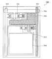
- FIG. 1is a diagram showing a layout of a light emitting pixel 700 included in a conventional light emitting display device shown in Patent Document 1.
- a signal line 705, a scanning line 706, and a power supply line 707are wired in the light emitting pixel 700.
- the light emitting pixel 700includes a switching transistor 701, a holding capacitor 702, a driving transistor 703, and a light emitting element 704.
- the light emitting element 704is formed in the light emitting region of the light emitting pixel 700, and the switching transistor 701, the holding capacitor 702, and the driving transistor 703 are formed in the driving circuit region.
- the holding capacitor 702occupies a large part of the drive circuit area. Therefore, when the holding capacitor 702 having a larger area is provided, or when other capacitors are provided, the region where the driving transistor 703 and the switching transistor 701 are arranged becomes narrow. Or a light emission area
- the present inventionhas been made to solve the above-described conventional problems, and the degree of freedom in design can be increased by providing a capacitor without providing a capacitor-dedicated region or newly increasing the capacitor.
- An objectis to provide a light-emitting display device.
- a light-emitting display deviceincludes a substrate, a semiconductor layer provided above the substrate, including a channel region, a source region, and a drain region, and a gate provided on the semiconductor layer.
- a thin film transistorincluding an insulating film, a gate electrode provided on the gate insulating film, and a source electrode and a drain electrode electrically connected to the source region and the drain region of the semiconductor layer, and the gate electrode
- An interlayer insulating filmprovided on the light emitting element, a light emitting element driven to emit light by a driving circuit configured using the thin film transistor, and a first region disposed on the interlayer insulating film in a region above the gate electrode.
- a capacitor electrode, and the first capacitor electrodeforms a first capacitor with the gate electrode.
- a light emitting display devicethat can increase the degree of freedom of design by providing a capacitor without installing or increasing an area dedicated to the capacitor.
- FIG. 1is a diagram illustrating a layout of pixels included in a conventional light emitting display device.
- FIG. 2is a block diagram illustrating an example of a configuration of the light-emitting display device according to Embodiment 1.
- FIG. 3is a diagram illustrating a circuit configuration of a light emitting pixel included in the display unit according to the first embodiment.
- FIG. 4is a diagram showing an example of the layout of the light emitting pixels according to the first embodiment.
- FIG. 5is a cross-sectional view of the light emitting pixel according to the first embodiment.
- FIG. 6is a diagram illustrating a circuit configuration of a light emitting pixel according to a modification of the first embodiment.
- FIG. 1is a diagram illustrating a layout of pixels included in a conventional light emitting display device.
- FIG. 2is a block diagram illustrating an example of a configuration of the light-emitting display device according to Embodiment 1.
- FIG. 3is a diagram illustrating a circuit
- FIG. 7is a cross-sectional view of a light emitting pixel according to a modification of the first embodiment.
- FIG. 8is a diagram illustrating a circuit configuration of a light emitting pixel according to another modification of the first embodiment.
- FIG. 9is a cross-sectional view of a luminescent pixel according to another modification of the first embodiment.
- FIG. 10is a diagram illustrating a circuit configuration of a light emitting pixel included in the display unit according to the second embodiment.
- FIG. 11is a diagram illustrating an example of the layout of the light-emitting pixels according to the second embodiment.
- FIG. 12is a cross-sectional view of the luminescent pixel according to the second embodiment.
- FIG. 13is an external view of a television provided with a light-emitting display device according to the present invention.
- FIG. 14is a diagram showing an example of the layout of the light emitting pixels of another modification of the light emitting display device according to the present invention.
- a light-emitting display deviceincludes a substrate, a semiconductor layer provided over the substrate and including a channel region, a source region, and a drain region, a gate insulating film provided on the semiconductor layer, and the gate insulating film A gate electrode provided thereon, a thin film transistor including a source electrode and a drain electrode electrically connected to the source region and the drain region of the semiconductor layer, and an interlayer insulating film provided on the gate electrode A light emitting element driven to emit light by a driving circuit configured using the thin film transistor, and a first capacitor electrode disposed on the interlayer insulating film in a region above the gate electrode, The first capacitor electrode constitutes a first capacitor with the gate electrode.
- the capacitoris arranged so as to overlap the thin film transistor above the thin film transistor.
- the pixel spacecan be used effectively. Therefore, a complicated driving circuit including a large number of thin film transistors and a large number of capacitors can be formed in a limited area.
- the capacitormay be a capacitor for holding the gate voltage, or may be a capacitor for holding the threshold voltage Vth in the driver circuit.
- the light emitting display devicemay include a plurality of first capacitor electrodes, and the plurality of first capacitor electrodes may constitute a first capacitor with the gate electrode.
- the source electrode or the drain electrodemay constitute the same layer as the first capacitor electrode, and either the source electrode or the drain electrode may be electrically connected to the first capacitor electrode. .
- the other electrode of the two electrodes constituting the capacitor and the source electrode or the drain electrodecan be formed in one step.
- the light emitting elementis electrically connected to the source electrode or the drain electrode
- the thin film transistoris a driving transistor for supplying a driving current to the light emitting element
- the first capacitoris the driving transistor. It may be a capacitor for setting the value of the current flowing through the capacitor.
- the thin film transistoris a switching transistor that determines a timing for supplying a driving current to the light emitting element
- the first capacitoris a capacitor for initializing a capacitor for setting a current value of the driving current. It may be.
- the driving transistornot only the driving transistor but also the gate electrode of the switching transistor and one capacitor electrode of the capacitor can be used. Therefore, more thin film transistors and capacitors can be arranged by effectively using a limited pixel space.
- the light emitting display devicemay further include a second capacitor, and the second capacitor may be connected in parallel with the first capacitor.
- the second capacitoris provided in parallel, so that the capacitance can be increased by the amount of the second capacitor.
- the second capacitorincludes an upper second capacitor electrode and a lower second capacitor electrode, and one of the upper second capacitor electrode and the lower second capacitor electrode is electrically connected to the gate electrode, The other of the upper second capacitor electrode and the lower second capacitor electrode may be electrically connected to either the source electrode or the drain electrode.
- the capacitancecan be increased by the amount of the second capacitor, the voltage can be stabilized and crosstalk can be reduced even if there is a current leak.
- the upper second capacitor electrodemay constitute the same layer as any one of the source electrode and the drain electrode
- the lower second capacitor electrodemay constitute the same layer as the gate electrode
- One capacitor electrodemay be electrically connected to the upper second capacitor electrode and either the source electrode or the drain electrode.
- the capacitor electrodes constituting the first capacitor and the second capacitorcan be formed as the same layer, the manufacturing process can be reduced.
- the area of the lower surface of the first capacitor electrode constituting the first capacitor in the upper region of the gate electrodemay be 30% to 100% of the area of the upper surface of the gate electrode.
- the semiconductor layermay be formed of polysilicon.
- the light emitting elementmay be an organic electroluminescence element.
- the capacitance of the first capacitormay be 0.1 to 10 pF.
- the light emitting display devicemay be a top emission type, and the light emitting element may be formed on an upper layer of the first capacitor electrode.
- the light emitting display devicemay be a bottom emission type, and the thin film transistor and the first capacitor may be formed in a region other than the light emitting region in which the light emitting element is formed.
- the light-emitting display deviceincludes a drive transistor and a capacitor, and the gate electrode of the drive transistor is one of the two capacitor electrodes constituting the capacitor. Therefore, the capacitor is formed in a region including the gate electrode of the driving transistor and above the driving transistor.
- FIG. 2is a block diagram illustrating an electrical configuration of the light-emitting display device 10 according to the first embodiment.
- the light emitting display device 10 in the figureincludes at least a control circuit 20, a scanning line driving circuit 40, a signal line driving circuit 50, and a display unit 60.
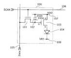
- FIG. 3is a diagram showing a circuit configuration of the light emitting pixel 100 included in the display unit 60 according to the first embodiment.
- the light emitting pixel 100 in FIG. 1includes a switching transistor 101, a capacitor 102, a driving transistor 103, an organic EL element 104, a signal line 105, a scanning line 106, a high voltage side power supply line 107, and a low voltage side power supply. Line 108.
- the control circuit 20has a function of controlling the scanning line driving circuit 40 and the signal line driving circuit 50.
- the control circuit 20outputs a video signal input from the outside to the signal line driving circuit 50 and controls the operation timing of the scanning line driving circuit 40 in accordance with the operation of the signal line driving circuit 50.
- the scanning line driving circuit 40is connected to the scanning line 106, and outputs a scanning signal to the scanning line 106, thereby switching the switching transistor 101 included in the light emitting pixel 100 between conduction (on state) and non-conduction (off state). It has a function to control.
- the signal line driving circuit 50is connected to the signal line 105 and has a function of outputting a signal voltage based on the video signal to the light emitting pixels 100.
- the display unit 60includes a plurality of light emitting pixels 100 arranged two-dimensionally, and displays an image based on a video signal input to the light emitting display device 10 from the outside.
- the switching transistor 101is an example of a switching element in which the gate is connected to the scanning line 106, one of the source and the drain is connected to the signal line 105, and the other of the source and the drain is connected to the capacitor electrode 102 a of the capacitor 102.
- the switching transistor 101has a function of determining the timing at which the signal voltage of the signal line 105 is applied to the capacitor electrode 102 a of the capacitor 102.
- the switching transistor 101is, for example, an n-type thin film transistor (n-type TFT), but may be a p-type TFT.
- the capacitor 102is an example of a first capacitor and includes two capacitor electrodes 102a and 102b.
- the capacitor electrode 102 ais connected to the gate of the driving transistor 103, and the capacitor electrode 102 b is connected to the high voltage side power supply line 107.
- the capacitor 102holds electric charge corresponding to the signal voltage supplied from the signal line 105. That is, the capacitor 102 is an example of a storage capacitor element for setting the current value of the drive current supplied to the organic EL element 104.
- the capacitor 102has a function of supplying a drive current from the drive transistor 103 to the organic EL element 104 until the next new signal voltage is written even after the switching transistor 101 is turned off.
- the drive transistor 103is an example of a drive element whose source is connected to the high-voltage power supply line 107 and whose drain is connected to the anode of the organic EL element 104.
- the drive transistor 103converts a voltage corresponding to the signal voltage applied between the gate and the source into a source-drain current corresponding to the signal voltage.
- the source-drain currentis supplied to the organic EL element 104 as a drive current.
- the drive transistor 103is, for example, a p-type thin film transistor (p-type TFT).
- the organic EL element 104is an example of a light emitting element that is driven to emit light by a drive circuit configured using a thin film transistor such as the drive transistor 103.
- the organic EL element 104has an anode connected to the drain of the drive transistor 103 and a cathode connected to the low-voltage power supply line 108.
- the organic EL element 104emits light when a driving current flows through the driving transistor 103.
- the emission intensityis controlled by the magnitude of the drive current, that is, the signal voltage.
- the signal line 105is connected to the signal line driving circuit 50, is connected to each light emitting pixel belonging to the pixel column including the light emitting pixel 100, and has a function of supplying a signal voltage for determining light emission intensity.
- the light emitting display device 10includes as many signal lines 105 as the number of pixel columns.
- the scanning line 106is connected to the scanning line driving circuit 40 and is connected to each light emitting pixel belonging to the pixel row including the light emitting pixel 100. Accordingly, the scanning line 106 has a function of supplying a timing for writing the signal voltage to each light emitting pixel belonging to the pixel row including the light emitting pixel 100. Note that the light emitting display device 10 includes the scanning lines 106 corresponding to the number of pixel rows.
- the high voltage side power supply line 107 and the low voltage side power supply line 108are also connected to other light emitting pixels and are connected to a voltage source.
- the potential difference between the voltage source VDD to which the high voltage side power supply line 107 is connected and the voltage source VEE to which the low voltage side power supply line 108 is connectedallows a current sufficient to cause the organic EL element 104 to emit light. It is a big size.
- the low-voltage power supply line 108may be grounded.
- the light-emitting display device 10includes a display unit 60 including a plurality of light-emitting pixels 100 arranged in a two-dimensional manner.
- the display unit 60displays an image when the organic EL element 104 in the light emitting pixel 100 emits light with a light emission intensity corresponding to the signal voltage.
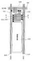
- FIG. 4is a diagram showing an example of the layout of the light emitting pixel 100 according to the first embodiment.
- the light emitting pixel 100is divided into a drive circuit region 110 and a light emitting region 120.
- An organic EL element 104is formed in the light emitting region 120, and the organic EL element 104 emits light according to a signal voltage supplied from the signal line 105.
- the light-emitting display device 10 according to Embodiment 1is a bottom-emission light-emitting display device. That is, the light emitted from the organic EL element 104 is emitted toward the back surface of the substrate. In other words, the display surface of the display unit 60 is the back side of the substrate.
- the drive circuit area 110is an area excluding the light emitting area 120 in the light emitting pixel 100, and is an area in which a drive circuit for driving the organic EL element 104 is formed.
- a switching transistor 101, a capacitor 102, and a drive transistor 103are formed in the drive circuit region 110.
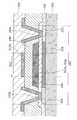
- FIG. 5is a cross-sectional view of the light-emitting pixel 100 according to the first embodiment. Specifically, FIG. 5 is a diagram schematically showing an AA cross section of the light emitting pixel 100 shown in FIG. A cross section AA is a cross section showing a positional relationship between the capacitor 102 and the driving transistor 103. For simplicity, the signal line 105 and the high-voltage power supply line 107 are not shown in FIG.
- the drive transistor 103is formed on the substrate 210.
- the driving transistor 103includes a semiconductor layer 220, a gate insulating film 230, a gate electrode 103g, a source electrode 103s, and a drain electrode 103d.
- the capacitor 102includes a capacitor electrode 102b, an interlayer insulating film 240, and a capacitor electrode 102a that also functions as the gate electrode 103g. Further, a planarization film 250 is formed on the capacitor 102.
- the substrate 210is a transparent substrate having transparency such as glass and quartz.
- the substrate 210may be a flexible substrate such as plastic.
- the substrate 210may be a semiconductor substrate such as a silicon substrate or a compound semiconductor substrate made of a compound semiconductor such as a nitride semiconductor.
- the driving transistor 103is formed on the substrate 210, it may be formed above the substrate 210.
- a buffer layermay be formed over the substrate 210, and the driving transistor 103 may be formed over the buffer layer.
- the semiconductor layer 220is a semiconductor layer formed on the substrate 210, and includes a channel region 221, a source region 222, and a drain region 223.
- the semiconductor layer 220is made of an inorganic semiconductor such as polysilicon doped with impurities, microcrystalline silicon, or amorphous silicon, or an organic semiconductor.
- the driving transistor 103is a p-type TFT, holes mainly contribute to conduction in the channel region 221. That is, according to the voltage applied to each of the source electrode 103s, the drain electrode 103d, and the gate electrode 103g, holes move from the source region 222 to the drain region 223, whereby the driving current described above flows.
- the gate insulating film 230is an insulating film such as a silicon oxide film (SiOx), for example.
- the gate insulating film 230is formed on the entire surface of the substrate 210 so as to cover the semiconductor layer 220, and through holes are formed in regions above the source region 222 and the drain region 223. Note that the gate insulating film 230 may be formed at least over the channel region 221.
- the gate electrode 103gis a metal electrode formed on the gate insulating film 230.
- the gate electrode 103ghas a single layer structure such as a metal such as molybdenum or tungsten, molybdenum / tungsten alloy, polysilicon, or a stacked structure of polysilicon, titanium, tungsten, and the like.
- the gate electrode 103gis connected to the source or drain of the switching transistor 101 (not shown in FIG. 5). The point that the gate electrode 103g also functions as the capacitor electrode 102a of the capacitor 102 is the greatest feature of the present invention.
- the source electrode 103 sis formed on the source region 222 and has a stacked structure of a metal such as aluminum or copper or a metal such as aluminum and molybdenum.
- the source electrode 103sis connected to the high voltage side power supply line 107 (not shown in FIG. 5). Further, as shown in FIG. 5, the source electrode 103 s is connected to the capacitor electrode 102 b of the capacitor 102 through a through hole formed in the interlayer insulating film 240 and the gate insulating film 230.
- the drain electrode 103dis formed on the drain region 223, and has a stacked structure of a metal such as aluminum or a metal such as aluminum and molybdenum.
- the drain electrode 103dis connected to the anode of the organic EL element 104 (not shown in FIG. 5).
- the interlayer insulating film 240is formed on the gate electrode 103g, and is made of, for example, a silicon nitride film (SiNx), a silicon oxide film, or the like. In the example shown in FIG. 5, the interlayer insulating film 240 is formed on the entire surface of the gate insulating film 230 so as to cover the gate electrode 103g, and through holes are formed in the information regions of the source region 222 and the drain region 223. Note that the interlayer insulating film 240 may be formed at least over the gate electrode 103g.
- the thickness of the interlayer insulating film 240is 100 to 1000 nm.
- the capacitor electrode 102bis an example of a first capacitor electrode, and is formed above the gate electrode 103g and on the interlayer insulating film 240. That is, the capacitor electrode 102b is disposed in the region above the gate electrode 103g and on the interlayer insulating film 240.
- the capacitor electrode 102bconstitutes the capacitor 102 together with the gate electrode 103g which is the other capacitor electrode 102a.
- the capacitor electrode 102bhas a stacked structure of a metal such as aluminum or copper, or a metal such as aluminum and molybdenum. In this example, the capacitor electrode 102 b is connected to the high voltage side power supply line 107.
- the capacitor electrode 102bconstitutes the same layer as the source electrode 103s and is connected to the source electrode 103s. Specifically, the capacitor electrode 102 b is connected to the source electrode 103 s through a through hole formed in the interlayer insulating film 240.
- the capacitor electrode 102bis preferably made of the same material as the source electrode 103s. Accordingly, the capacitor electrode 102b and the source electrode 103s can be formed in the same process, and the number of processes can be reduced.
- the area of the lower surface of the capacitor electrode 102b in the upper region of the gate electrode 103g that is the capacitor electrode 102ais 30% to 100% of the area of the upper surface of the gate electrode 103g. Note that the capacitor electrode 102b may be larger than the gate electrode 103g.
- the capacitance of the capacitor 102is 0.1 to 10 pF.
- the planarizing film 250is formed on the capacitor 102 and functions as a protective film that protects the capacitor 102 and the driving transistor 103, and also functions as a planarizing film that planarizes the upper side of the capacitor 102 and the driving transistor 103.
- the planarization film 250is made of, for example, a silicon oxide film (SiOx) or a silicon nitride film (SiNx).
- the capacitor 102uses the gate electrode 103g as one electrode. That is, the capacitor 102 including the gate electrode 103g as the capacitor electrode 102a is formed in a region above the driving transistor 103.
- the capacitor 102can be disposed without providing a region dedicated to the capacitor 102 in the light emitting pixel 100. Therefore, the area of the capacitor 102 or the arrangement of the driving transistor 103 and the switching transistor 101 can be designed relatively freely. Alternatively, other capacitors can be added to the drive circuit region 110.
- the degree of freedom in designcan be improved. Thereby, for example, since the light emitting display device 10 according to Embodiment 1 is a bottom emission type, the light emitting region 120 can be secured widely, and the current density flowing through the organic EL element 104 can be reduced. The light emission lifetime of the light emitting display device 10 can be secured longer.
- the structure in which the capacitor is formed above the driving transistor 103can be applied to other driving circuits other than the circuit shown in FIG.
- the configuration according to the present embodimentcan be applied to a drive circuit having a circuit configuration in which the gate of the drive transistor 103 and one of two capacitor electrodes constituting the capacitor are electrically connected. it can.
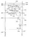
- FIG. 6is a diagram illustrating a circuit configuration of a light emitting pixel 300 according to a modification of the first embodiment. 6 includes a switching transistor 101, 313, 314, and 315, a driving transistor 103, capacitors 311 and 312, an organic EL element 104, a signal line 105, scanning lines 106, 316, 317, and 318, a high-voltage power supply line 107, a low-voltage power supply line 108, and a reference voltage power supply line 319.
- symbolis attached
- the switching transistor 313has a gate connected to the scanning line 316, one of the source and the drain connected to the reference voltage power supply line 319, and the other of the source and the drain connected to one of the source and the drain of the switching transistor 101. It is an example.
- the switching transistor 313has a function of initializing the gate potential of the driving transistor 103, that is, setting the reference potential Vref.
- the switching transistor 313is turned on by the scanning signal supplied from the scanning line 316, and supplies the reference potential Vref to the second electrode of the capacitor.
- the switching transistor 313is, for example, an n-type TFT.
- the switching transistor 314is an example of a switching element in which the gate is connected to the scanning line 317, one of the source and the drain is connected to the gate of the driving transistor 103, and the other of the source and the drain is connected to the drain of the driving transistor 103. .
- the switching transistor 314has a function of detecting the threshold voltage of the driving transistor 103.
- the switching transistor 314is turned on by a scanning signal supplied from the scanning line 317 and short-circuits the gate and drain of the driving transistor 103. Therefore, the threshold voltage of the drive transistor 103 is generated at the gate electrode of the drive transistor 103.
- the switching transistor 314is, for example, an n-type TFT.
- the switching transistor 315is an example of a switching element in which the gate is connected to the scanning line 318, one of the source and the drain is connected to the drain of the driving transistor 103, and the other of the source and the drain is connected to the anode of the organic EL element 104. is there.
- the switching transistor 315has a function of determining timing for supplying a drive current to the organic EL element 104.
- the switching transistor 315is turned on by a scanning signal supplied from the scanning line 318, and a driving current is supplied to the organic EL element 104 if the driving transistor 103 is turned on during the on state. Is done. In other words, if the switching transistor 315 is off, no current is supplied to the organic EL element 104 regardless of the operation of the drive transistor 103.
- the switching transistor 315is, for example, an n-type TFT.
- the capacitor 311includes two capacitor electrodes 311a and 311b.
- the capacitor electrode 311 ais connected to the reference voltage power supply line 319, and the capacitor electrode 311 b is connected to one of the source and drain of the switching transistor 101.
- the capacitor electrode 311bis connected to the gate of the driving transistor 103 via the capacitor 312.
- the capacitor 311holds charges corresponding to the signal voltage supplied from the signal line 105.
- the capacitor 312is an example of a first capacitor, and includes two capacitor electrodes 312a and 312b.
- the capacitor electrode 312 ais connected to one of the source and the drain of the switching transistor 101, and the capacitor electrode 312 b is connected to the gate of the drive transistor 103.
- the capacitor 312holds electric charge corresponding to the threshold voltage of the driving transistor 103.
- the scanning lines 316, 317, and 318are connected to the scanning line driving circuit 40 and connected to each light emitting pixel belonging to the pixel column including the light emitting pixels 300.
- the scanning line 316has a function of supplying a reference voltage for detecting the threshold voltage of the driving transistor 103 included in each light emitting pixel belonging to the pixel row including the light emitting pixel 300.
- the scanning line 317has a function of supplying timing for detecting the threshold voltage of the driving transistor 103 included in each light emitting pixel belonging to the pixel row including the light emitting pixel 300.
- the scanning line 318has a function of supplying a timing for supplying a driving current to the organic EL element 104 included in each light emitting pixel belonging to the pixel row including the light emitting pixels 300 and a timing for detecting a threshold voltage of the driving transistor 103.
- the light emitting display device 10includes scanning lines 316, 317, and 318 corresponding to the number of pixel rows.
- the reference voltage power line 319is also connected to other light emitting pixels, and is connected to a voltage source that supplies a predetermined reference voltage. As a result, the potential of the reference voltage power supply line 319 is maintained at the reference potential Vref.
- FIG. 7is a cross-sectional view of a part of a luminescent pixel 300 according to a modification of the first embodiment. Specifically, FIG. 7 shows an arrangement configuration of the capacitor 312 and the driving transistor 103. Note that the cross-sectional configuration of the drive transistor 103 is the same as the cross-sectional configuration illustrated in FIG.
- a capacitor electrode 312 b of the capacitor 312is formed on the interlayer insulating film 240.
- the gate electrode 103galso functions as the capacitor electrode 312a of the capacitor 312.
- the capacitor electrode 312bis an example of a first capacitor electrode, and is not connected to the source electrode 103s or the drain electrode 103d of the driving transistor 103.
- the capacitor electrode 312bis connected to one of the source and drain of the switching transistor 101 and the capacitor electrode 311b (not shown in FIG. 7).
- the capacitor electrode 312b of the capacitor 311 formed on the driving transistor 103may not be connected to each electrode of the driving transistor 103. That is, as long as one of the two electrodes constituting the capacitor is connected to the gate electrode 103g of the driving transistor 103, the structure according to this embodiment can be applied.
- FIG. 8is a diagram illustrating a circuit configuration of a light emitting pixel 400 according to another modification of the first embodiment.
- the light emitting pixel 400 shown in FIG. 8is different from the light emitting pixel 300 shown in FIG. 6 in that a capacitor 411 is provided instead of the capacitor 311 and a switching transistor 413 is provided instead of the switching transistor 313.
- a capacitor 411is provided instead of the capacitor 311
- a switching transistor 413is provided instead of the switching transistor 313.
- the capacitor 411is an example of a first capacitor, and includes two capacitor electrodes 411a and 411b.
- the capacitor electrode 411ais connected to the gate electrode 103g of the driving transistor 103, and the capacitor electrode 411b is connected to, for example, the high voltage side power supply line 107.
- the capacitor 411holds charges corresponding to the signal voltage supplied from the signal line 105 and the threshold voltage of the driving transistor.
- the switching transistor 413has a gate connected to the scanning line 316, one of the source and the drain connected to the high-voltage power supply line 107, the other of the source and the drain connected to one of the source and the drain of the switching transistor 101, and the capacitor of the capacitor 312. It is an example of the switching element connected to the electrode 312b.
- the switching transistor 413has a function of initializing the capacitor 312 and the capacitor 411.
- the switching transistor 413is turned on by a scanning signal supplied from the scanning line 316, sets the potential of the capacitor electrode 312b of the capacitor 312 to VDD, and the scanning transistor 314 is supplied from the scanning line 317.
- the capacitor 312 and the capacitor 411are initialized so that the threshold voltage of the driving transistor 103 is held.
- the switching transistor 413is, for example, an n-type TFT.
- FIG. 9is a cross-sectional view of a light emitting pixel 400 according to a modification of the first embodiment. Specifically, FIG. 9 shows an arrangement configuration of the capacitor 312, the capacitor 411, and the driving transistor 103. Note that the cross-sectional configuration of the drive transistor 103 is the same as the cross-sectional configuration illustrated in FIG.
- the capacitor electrode 312 b of the capacitor 312 and the capacitor electrode 411 b of the capacitor 411are formed on the interlayer insulating film 240.
- the gate electrode 103galso functions as the capacitor electrode 312a of the capacitor 312 and the capacitor electrode 411a of the capacitor 411.
- the capacitor electrode 411bis an example of a first capacitor electrode, forms the same layer as the source electrode 103s of the driving transistor 103, and is connected to the source electrode 103s. Specifically, the capacitor electrode 411 b is connected to the source electrode 103 s through a through hole formed in the interlayer insulating film 240.
- the capacitor electrode 312b, the capacitor electrode 411b, and the source electrode 103sare preferably made of the same material. Accordingly, the capacitor electrode 312b, the capacitor electrode 411b, and the source electrode 103s can be formed in the same process, so that the number of processes can be reduced.
- the light-emitting display device 10includes the plurality of first capacitor electrodes, and the plurality of first capacitor electrodes includes the first capacitor between the gate electrode 103g. It is composed.
- the plurality of first capacitor electrodesincludes the first capacitor between the gate electrode 103g. It is composed.
- two first capacitor electrodesare shown, but three or more first capacitor electrodes are formed in the region above the gate electrode 103 g and on the interlayer insulating film 240. May be.
- the first capacitoris formed by the gate electrode 103g of the drive transistor 103 included in the drive circuit and the first capacitor electrode formed above the gate electrode 103g. Configure.
- the first capacitor thus configuredcan be used as a storage capacitor element for setting the current value of the drive current supplied to the organic EL element 104.
- the light emitting display device 10has an effect that, for example, a wide light emitting region 120 can be secured.
- the light-emitting display device 10may further include a second capacitor connected in parallel with the capacitor 102.
- the second capacitorincludes an upper second capacitor electrode and a lower second capacitor electrode.
- One of the upper second capacitor electrode and the lower second capacitor electrodeis connected to the gate electrode 103g, and the other is electrically connected to one of the source electrode 103s and the drain electrode 103d.
- the lower second capacitor electrodeconstitutes the same layer as the gate electrode 103g
- the upper second capacitor electrodeis the same as one of the electrically connected source electrode 103s and drain electrode 103d. It may constitute a layer.
- the capacitor electrode 102a of the capacitor 102is electrically connected to the upper second capacitor electrode.
- the light-emitting display deviceincludes a switching transistor, a driving transistor, and a capacitor, and the gate electrode of the switching transistor is one of the two capacitor electrodes that form the capacitor. Therefore, the capacitor is formed in the region above the switching transistor.
- the light emitting display deviceis different from the light emitting display device 10 according to the first embodiment in the circuit configuration of the light emitting pixels included in the display unit and the arrangement of the elements constituting the light emitting pixels. . That is, the electrical configuration of the light-emitting display device according to Embodiment 2 is the same as that of the light-emitting display device 10 according to Embodiment 1 shown in FIG. Therefore, in the following, description of the electrical configuration of the light-emitting display device according to Embodiment 2 will be omitted, and description will be made focusing on the circuit configuration of the light-emitting pixel and the arrangement of elements constituting the light-emitting pixel.
- FIG. 10is a diagram illustrating a circuit configuration of the light-emitting pixel 500 included in the display unit according to the second embodiment.
- the light-emitting pixel 500 in the figureincludes switching transistors 501, 506, 507, and 508, capacitors 502 and 505, a driving transistor 503, an organic EL element 504, a signal line 509, scanning lines 510, 511, 512, and 513.
- the switching transistor 501has a gate connected to the scanning line 510, one of the source and drain connected to the signal line 509, and the other connected to the capacitor electrode 502 a of the capacitor 502 and the gate of the driving transistor 503. It is an example of an element.
- the switching transistor 501has a function of determining timing for applying the signal voltage of the signal line 509 to the capacitor electrode 502 a of the capacitor 502.
- the switching transistor 501is, for example, an n-type TFT.
- the capacitor 502is an example of a first capacitor for the driving transistor 503, and includes two capacitor electrodes 502a and 502b.
- the capacitor electrode 502 ais connected to the gate of the driving transistor 503, and the capacitor electrode 502 b is connected to the capacitor electrode 505 b of the capacitor 505 and the source or drain of the switching transistor 507.
- the capacitor 502holds electric charge corresponding to the signal voltage supplied from the signal line 509 and the threshold voltage of the driving transistor 503. That is, the capacitor 502 is an example of a storage capacitor element for setting the current value of the drive current supplied to the organic EL element 504.
- the drive transistor 503is an example of a drive element whose drain is connected to the high-voltage power supply line 514 and whose source is connected to the anode of the organic EL element 504 via the switching transistor 508.
- the driving transistor 503converts a voltage corresponding to the signal voltage applied between the gate and the source into a source-drain current corresponding to the signal voltage.
- the drive transistor 503is, for example, an n-type TFT.
- the organic EL element 504is an example of a light emitting element having an anode connected to the source of the drive transistor 503 via the switching transistor 508 and a cathode connected to the low-voltage power supply line 515.
- the organic EL element 504emits light when a driving current flows through the driving transistor 503.
- the capacitor 505is an example of a first capacitor for the switching transistor 508, and includes two capacitor electrodes 505a and 505b.
- the capacitor electrode 505ais connected to the scanning line 513, and the capacitor electrode 505b is connected to one of the source and drain of the capacitor electrode 502b and the switching transistor 507.
- the capacitor 505is an example of a capacitor element for adjusting the amount of voltage held by the capacitor 502 serving as a holding capacitor element for the data voltage applied from the signal line 509.
- the switching transistor 506is an example of a switching element in which the gate is connected to the scanning line 511, one of the source and the drain is connected to the reference voltage power supply line 516, and the other of the source and the drain is connected to the gate of the driving transistor 503. .
- the switching transistor 506has a function of applying a reference voltage Vref to the gate of the driving transistor 503. Note that the switching transistor 506 is, for example, an n-type TFT.
- the switching transistor 507is an example of a switching element in which the gate is connected to the scanning line 512, one of the source and the drain is connected to the capacitor electrode 502 b of the capacitor 502, and the other of the source and the drain is connected to the source of the driving transistor 503. is there.
- the switching transistor 507has a function of disconnecting the capacitor 502 and the source of the driving transistor 503 when a signal voltage is written to the capacitor 502.
- the switching transistor 507is, for example, an n-type TFT.
- the switching transistor 508is an example of a switching element in which the gate is connected to the scanning line 513, one of the source and the drain is connected to the source of the driving transistor 503, and the other of the source and the drain is connected to the anode of the organic EL element 504. is there.
- the switching transistor 508has a function of determining timing for supplying a drive current to the organic EL element 504. Note that the switching transistor 508 is, for example, an n-type TFT.
- the signal line 509is connected to the signal line driving circuit, is connected to each light emitting pixel belonging to the pixel column including the light emitting pixel 500, and has a function of supplying a signal voltage for determining light emission intensity.
- the light-emitting display deviceincludes as many signal lines 509 as the number of pixel columns.
- the scanning lines 510, 511, 512 and 513are connected to the scanning line driving circuit and connected to each light emitting pixel belonging to the pixel row including the light emitting pixel 500.
- the scanning line 510has a function of supplying timing for writing the signal voltage to each light emitting pixel belonging to the pixel row including the light emitting pixel 500.
- the scanning line 511has a function of supplying timing for applying the reference voltage Vref to the gate of the driving transistor 503 in each light emitting pixel belonging to the pixel row including the light emitting pixel 500.
- the scanning line 512has a function of supplying timing for disconnecting the capacitor 502 and the source of the driving transistor 503 in each light emitting pixel belonging to the pixel row including the light emitting pixel 500.
- the scanning line 513has a function of supplying timing for supplying a driving current to the organic EL element 504 in each light emitting pixel belonging to the pixel row including the light emitting pixel 500.
- the light-emitting display deviceincludes scan lines 510, 511, 512, and 513 corresponding to the number of pixel rows.
- the high voltage side power supply line 514, the low voltage side power supply line 515, and the reference voltage power supply line 516are also connected to other light emitting pixels and connected to the voltage source. ing.
- the potential difference between the voltage source to which the high voltage side power supply line 514 is connected and the voltage source to which the low voltage side power supply line 515 is connectedis large enough to allow a current sufficient to cause the organic EL element 504 to emit light. That's it.
- the low voltage side power supply line 515may be grounded.
- FIG. 11is a diagram showing an example of the layout of the light emitting pixel 500 according to the second embodiment.
- the light-emitting display device according to Embodiment 2is a top emission type light-emitting display device. That is, the light emitted from the organic EL element 504 is emitted toward the surface of the substrate. In other words, the display surface of the display unit is the surface side of the substrate.
- the light emitting region where the organic EL element 504 is formed and the drive circuit regionare the same. That is, a light emitting region is formed above the drive circuit region.
- the driving transistor 503 and the capacitor 502are formed to overlap the same region in the plane, and the switching transistor 508 and the capacitor 505 are formed to overlap the same region in the plane.
- the structure according to this embodimentcan be applied to any circuit structure in which the gate of the thin film transistor such as the driving transistor 503 or the switching transistor 508 is electrically connected to the capacitor electrode of the capacitor. .
- FIG. 12is a cross-sectional view of the light-emitting pixel 500 according to the second embodiment. Specifically, FIG. 12 shows an arrangement configuration of the switching transistor 508, the capacitor 505, and the organic EL element 504.
- the configuration of the switching transistor 508is the same as that of the driving transistor 103 shown in FIG. That is, the substrate 610, the semiconductor layer 620, the gate insulating film 630, the interlayer insulating film 640, the gate electrode 508g, the source electrode 508s, and the drain electrode 508d shown in FIG. 12 are respectively the substrate 210, the semiconductor layer 220, and the gate insulating film shown in FIG. It corresponds to the film 230, the interlayer insulating film 240, the gate electrode 103g, the source electrode 103s, and the drain electrode 103d. Further, the channel region 621, the source region 622, and the drain region 623 included in the semiconductor layer 620 correspond to the channel region 221, the source region 222, and the drain region 223 included in the semiconductor layer 220, respectively.
- the capacitor electrode 505b of the capacitor 505is an example of a first capacitor electrode, forms the same layer as the source electrode 508s, and is electrically connected to the source electrode 508s. Note that the capacitor electrode 505b may be electrically connected to the drain electrode 508d instead of the source electrode 508s.
- the organic EL element 504is formed in an upper layer of the capacitor 505. Specifically, as shown in FIG. 12, an organic EL element 504 is formed through a planarizing film 650 formed on the capacitor 505.
- the organic EL element 504includes an anode 504a, a light emitting layer 504b, and a transparent cathode 504c.
- the planarizing film 650is made of, for example, a silicon nitride film.
- the anode 504ais an electrode having light reflectivity and is made of, for example, a metal such as aluminum.
- the anode 504ahas a function of reflecting light emitted from the light emitting layer 504b.
- the anode 504ais an anode electrode of the organic EL element 504, and is connected to the source of the driving transistor 503 via the switching transistor 508 as shown in FIG.
- the light emitting layer 504bis a light emitting layer that is formed between the anode 504a and the transparent or translucent transparent cathode 504c and emits light by recombination of holes and electrons injected from the anode 504a and the transparent cathode 504c.
- the light-emitting layer 504bmay include a hole transport layer, a hole injection layer, an electron transport layer, an electron injection layer, and the like.
- the transparent cathode 504cis an electrode having optical transparency, and is made of a transparent oxide conductive film such as indium tin oxide (ITO), for example.
- the transparent cathode 504cis a cathode electrode of the organic EL element 504, and is connected to the low voltage side power supply line 515 as shown in FIG.
- the capacitor 505includes the gate electrode 508g of the switching transistor 508 included in the drive circuit and the capacitor electrode 505b formed above the gate electrode 508g.
- the capacitor 505 configured as described aboveinitializes a storage capacitor element for setting a current value of a drive current supplied to the organic EL element 504, for example, and the storage capacitor has a data voltage applied from the signal line 509. Of these, it can be used as a capacitive element for adjusting the amount of voltage to be held.
- the configuration of this embodimentcan be applied to any drive circuit having a circuit configuration in which the gate electrode of the switching transistor and one of the capacitor electrodes of the capacitor are electrically connected.
- the area dedicated to the capacitorcan be reduced, and the degree of freedom in designing the drive circuit can be increased.
- the light emitting display devicehas been described based on the embodiments, but the present invention is not limited to these embodiments. Unless it deviates from the meaning of this invention, the form which carried out the various deformation
- the present inventioncan be applied to a circuit having a circuit configuration in which a gate of a thin film transistor included in a driving circuit and one of electrodes of a capacitor are connected.
- a circuit configurationin which a gate of a thin film transistor included in a driving circuit and one of electrodes of a capacitor are connected.
- the configuration in which the gate of the driving transistor or the switching transistor and one of the electrodes of the capacitor are connectedis described.
- the circuit configurationis not limited to the above description.
- the n-type transistor that is turned on when a positive voltage is applied to the gate of the switching transistorhas been described. Even if the video display device has the polarity reversed, the same effects as those of the above-described embodiments can be obtained.
- the lower electrodeis an anode and the upper electrode is a cathode.
- the lower electrodemay be a cathode and the upper electrode may be an anode.
- the light emitting display device according to the present inventionis built in a television as shown in FIG.
- a televisioncapable of displaying images with high accuracy reflecting a video signal is realized.
- the light emitting display devicemay include a second capacitor that is electrically connected in parallel with the first capacitor including the gate electrode of the thin film transistor as described above as a lower electrode.
- FIG. 14is a diagram showing an example of the layout of the light emitting pixels of another modification of the light emitting display device according to the present invention.
- the same components as those of the conventional light emitting display device shown in FIG. 1are denoted by the same reference numerals, and description thereof is omitted below.
- the light emitting pixel 700includes a first capacitor 708 and a holding capacitor 702 which is a second capacitor.
- the first capacitor 708is formed on the driving transistor 703 and includes an upper electrode and a lower electrode.
- the lower electrode of the first capacitor 708also functions as the gate electrode of the driving transistor 703.
- the holding capacitor 702 as the second capacitorincludes an upper second capacitor electrode and a lower second capacitor electrode.
- the upper electrode of the first capacitor 708is electrically connected to the upper second capacitor electrode of the holding capacitor 702. Specifically, as shown in FIG. 14, the upper electrode of the first capacitor 708 is the same as the upper second capacitor electrode of the holding capacitor 702, the power supply line 707, and one of the source electrode and the drain electrode of the driving transistor 703. And is electrically connected to one of the layers.
- the lower electrode of the first capacitor 708functions as the gate electrode of the driving transistor 703 and is electrically connected to the lower second capacitor electrode of the holding capacitor 702.
- the gate electrode which is the lower electrode of the first capacitor 708forms the same layer as the lower second capacitor electrode of the holding capacitor 702 and is electrically connected.
- the region above the driving transistor 703can be used effectively, and the capacitance of the holding capacitor 702 can be increased.
- the light-emitting display devicecan be used for all display devices such as a television, a personal computer, and a mobile phone.
- Scan line drive circuit50
- Signal line drive circuit 60Display part 100,300,400,500,700 Light emission pixel 101,313,314,315,413,501,506,507,508,701 Switching transistors 102, 311, 312, 411, 502, 505 Capacitors 102a, 102b, 311a, 311b, 312a, 312b, 411a, 411b, 502a, 502b, 505a, 505b Capacitor electrodes 103, 503, 703 Driving transistors 103d, 508d Drain Electrodes 103g, 508g Gate electrodes 103s, 508s Source electrodes 104, 504 Organic EL elements 105, 509, 705 Signal lines 106, 316, 317, 318, 510, 511, 512, 513, 70 Scan line 107, 514 High voltage side power supply line 108, 515 Low voltage side power supply line 110 Drive circuit region 120
Landscapes
- Engineering & Computer Science (AREA)
- Physics & Mathematics (AREA)
- Geometry (AREA)
- Microelectronics & Electronic Packaging (AREA)
- Computer Hardware Design (AREA)
- General Physics & Mathematics (AREA)
- Theoretical Computer Science (AREA)
- Electroluminescent Light Sources (AREA)
- Control Of Indicators Other Than Cathode Ray Tubes (AREA)
- Devices For Indicating Variable Information By Combining Individual Elements (AREA)
- Control Of El Displays (AREA)
Abstract
Description
Translated fromJapanese本発明は、発光表示装置に関し、特に、キャパシタと薄膜トランジスタとを含む駆動回路と発光素子とを備えるアクティブマトリクス型の発光表示装置に関する。The present invention relates to a light-emitting display device, and more particularly to an active matrix light-emitting display device including a drive circuit including a capacitor and a thin film transistor and a light-emitting element.
従来、有機エレクトロルミネッセンス素子(以下、有機EL素子と記載する)などの、電流によって輝度を制御する発光素子を2次元状に配列した発光表示装置の開発が盛んに行われている。特に、発光素子を駆動するための駆動回路を発光素子毎に備えた画素回路を配列したアクティブマトリクス型の発光表示装置の開発が行われている。2. Description of the Related Art Conventionally, light-emitting display devices in which light-emitting elements whose luminance is controlled by current, such as organic electroluminescence elements (hereinafter referred to as organic EL elements), are two-dimensionally arranged have been actively developed. In particular, an active matrix light-emitting display device in which pixel circuits each having a driving circuit for driving a light-emitting element are arranged has been developed.
駆動回路は、一般的に、発光する画素を選択するスイッチングトランジスタと、発光素子を駆動する駆動トランジスタと、キャパシタとを備える。駆動回路は、例えば、駆動トランジスタが流す電流量を決定するための電圧を保持する保持キャパシタを備えている(特許文献1参照)。The drive circuit generally includes a switching transistor that selects a pixel that emits light, a drive transistor that drives the light emitting element, and a capacitor. The drive circuit includes, for example, a holding capacitor that holds a voltage for determining the amount of current flowing through the drive transistor (see Patent Document 1).
図1は、特許文献1に示す従来の発光表示装置が備える発光画素700のレイアウトを示す図である。図1に示すように、発光画素700には、信号線705と、走査線706と、電源線707とが配線されている。また、発光画素700は、スイッチングトランジスタ701と、保持キャパシタ702と、駆動トランジスタ703と、発光素子704とを備える。発光素子704は、発光画素700の発光領域に形成され、スイッチングトランジスタ701と、保持キャパシタ702と、駆動トランジスタ703とは、駆動回路領域に形成されている。FIG. 1 is a diagram showing a layout of a
しかしながら、上記従来技術では、キャパシタ専用の領域が設けられることになり、キャパシタの数、又は、キャパシタの面積が増えた場合に、その他の素子を配置する領域が狭くなり、設計の自由度が下がるという課題がある。However, in the above prior art, a capacitor-dedicated region is provided, and when the number of capacitors or the area of the capacitor increases, the region where other elements are arranged becomes narrow, and the degree of freedom in design decreases. There is a problem.
例えば、図1に示す特許文献1に記載の発光表示装置のように、駆動回路領域の多くの部分を保持キャパシタ702が占めている。したがって、より大きな面積の保持キャパシタ702を備える場合、又は、その他のキャパシタを備える場合には、駆動トランジスタ703及びスイッチングトランジスタ701を配置する領域が狭くなる。あるいは、発光領域が小さくなってしまい、発光素子に流れる電流密度が上昇し寿命が短くなってしまう。For example, like the light emitting display device described in
そこで、本発明は、上記従来の課題を解決するためになされたものであり、キャパシタ専用の領域を設置、又は、新たに増やすことなくキャパシタを設けることで、設計の自由度を高めることができる発光表示装置を提供することを目的とする。Therefore, the present invention has been made to solve the above-described conventional problems, and the degree of freedom in design can be increased by providing a capacitor without providing a capacitor-dedicated region or newly increasing the capacitor. An object is to provide a light-emitting display device.
上記目的を達成するため、本発明に係る発光表示装置は、基板と、該基板の上方に設けられ、チャネル領域、ソース領域、及びドレイン領域を含む半導体層、該半導体層上に設けられたゲート絶縁膜、該ゲート絶縁膜上に設けられたゲート電極、並びに、前記半導体層の前記ソース領域及び前記ドレイン領域にそれぞれ電気的に接続されたソース電極及びドレイン電極を含む薄膜トランジスタと、前記ゲート電極上に設けられた層間絶縁膜と、前記薄膜トランジスタを用いて構成される駆動回路によって発光駆動される発光素子と、前記ゲート電極の上方領域内であって、前記層間絶縁膜上に配置された第1キャパシタ電極とを備え、該第1キャパシタ電極は、前記ゲート電極との間で第1キャパシタを構成している。In order to achieve the above object, a light-emitting display device according to the present invention includes a substrate, a semiconductor layer provided above the substrate, including a channel region, a source region, and a drain region, and a gate provided on the semiconductor layer. A thin film transistor including an insulating film, a gate electrode provided on the gate insulating film, and a source electrode and a drain electrode electrically connected to the source region and the drain region of the semiconductor layer, and the gate electrode An interlayer insulating film provided on the light emitting element, a light emitting element driven to emit light by a driving circuit configured using the thin film transistor, and a first region disposed on the interlayer insulating film in a region above the gate electrode. A capacitor electrode, and the first capacitor electrode forms a first capacitor with the gate electrode.
本発明によれば、キャパシタ専用の領域を設置、又は増やすことなく、キャパシタを設けることで、設計の自由度を高めることができる発光表示装置を提供することができる。According to the present invention, it is possible to provide a light emitting display device that can increase the degree of freedom of design by providing a capacitor without installing or increasing an area dedicated to the capacitor.
以下、本発明に係る発光表示装置の実施の形態について、図面を参照しながら説明する。Hereinafter, embodiments of a light emitting display device according to the present invention will be described with reference to the drawings.
本発明に係る発光表示装置は、基板と、該基板の上方に設けられ、チャネル領域、ソース領域、及びドレイン領域を含む半導体層、該半導体層上に設けられたゲート絶縁膜、該ゲート絶縁膜上に設けられたゲート電極、並びに、前記半導体層の前記ソース領域及び前記ドレイン領域にそれぞれ電気的に接続されたソース電極及びドレイン電極を含む薄膜トランジスタと、前記ゲート電極上に設けられた層間絶縁膜と、前記薄膜トランジスタを用いて構成される駆動回路によって発光駆動される発光素子と、前記ゲート電極の上方領域内であって、前記層間絶縁膜上に配置された第1キャパシタ電極とを備え、該第1キャパシタ電極は、前記ゲート電極との間で第1キャパシタを構成している。A light-emitting display device according to the present invention includes a substrate, a semiconductor layer provided over the substrate and including a channel region, a source region, and a drain region, a gate insulating film provided on the semiconductor layer, and the gate insulating film A gate electrode provided thereon, a thin film transistor including a source electrode and a drain electrode electrically connected to the source region and the drain region of the semiconductor layer, and an interlayer insulating film provided on the gate electrode A light emitting element driven to emit light by a driving circuit configured using the thin film transistor, and a first capacitor electrode disposed on the interlayer insulating film in a region above the gate electrode, The first capacitor electrode constitutes a first capacitor with the gate electrode.
これにより、薄膜トランジスタのゲート電極を、単にゲート電極として利用するだけではなく、キャパシタを構成する2つの電極のうちの一方の電極としても利用するので、薄膜トランジスタの上方に薄膜トランジスタと重なるように、キャパシタを配置することができ、画素スペースを有効に活用することができる。したがって、多数の薄膜トランジスタ及び多数のキャパシタを含む複雑な駆動回路を、限られた面積の領域に形成することができる。なお、キャパシタは、ゲート電圧を保持するためのキャパシタであってもよく、駆動回路における閾値電圧Vthを保持するためのキャパシタであっても、本発明の構成を適用することができる。Thus, since the gate electrode of the thin film transistor is not only used as the gate electrode but also as one of the two electrodes constituting the capacitor, the capacitor is arranged so as to overlap the thin film transistor above the thin film transistor. The pixel space can be used effectively. Therefore, a complicated driving circuit including a large number of thin film transistors and a large number of capacitors can be formed in a limited area. Note that the capacitor may be a capacitor for holding the gate voltage, or may be a capacitor for holding the threshold voltage Vth in the driver circuit.
また、前記発光表示装置は、複数の前記第1キャパシタ電極を備え、複数の前記第1キャパシタ電極は、前記ゲート電極との間でそれぞれ第1キャパシタを構成していてもよい。Further, the light emitting display device may include a plurality of first capacitor electrodes, and the plurality of first capacitor electrodes may constitute a first capacitor with the gate electrode.
また、前記ソース電極またはドレイン電極が、前記第1キャパシタ電極と同一の層を構成し、該ソース電極またはドレイン電極のいずれか一方は、該第1キャパシタ電極と電気的に接続されていてもよい。The source electrode or the drain electrode may constitute the same layer as the first capacitor electrode, and either the source electrode or the drain electrode may be electrically connected to the first capacitor electrode. .
これにより、キャパシタを構成する2つの電極のうちの他方の電極とソース電極又はドレイン電極とを1つの工程で形成することができる。Thereby, the other electrode of the two electrodes constituting the capacitor and the source electrode or the drain electrode can be formed in one step.
また、前記発光素子は、前記ソース電極または前記ドレイン電極と電気的に接続されており、前記薄膜トランジスタは、前記発光素子に駆動電流を供給する駆動トランジスタであり、前記第1キャパシタは、前記駆動トランジスタに流れる電流値を設定するためのキャパシタであってもよい。The light emitting element is electrically connected to the source electrode or the drain electrode, the thin film transistor is a driving transistor for supplying a driving current to the light emitting element, and the first capacitor is the driving transistor. It may be a capacitor for setting the value of the current flowing through the capacitor.
これにより、駆動トランジスタに流れる駆動電流の電流値を設定するためのキャパシタを、画素スペースを有効に活用しつつ、駆動回路を構成することができる。Thereby, it is possible to configure a drive circuit while effectively utilizing the pixel space for the capacitor for setting the current value of the drive current flowing through the drive transistor.
また、前記薄膜トランジスタは、前記発光素子への駆動電流を供給するタイミングを決定するスイッチングトランジスタであり、前記第1キャパシタは、前記駆動電流の電流値を設定するためのキャパシタを初期化するためのキャパシタであってもよい。The thin film transistor is a switching transistor that determines a timing for supplying a driving current to the light emitting element, and the first capacitor is a capacitor for initializing a capacitor for setting a current value of the driving current. It may be.
これにより、駆動トランジスタに限らず、スイッチングトランジスタのゲート電極とキャパシタの一方のキャパシタ電極とも兼用させることができる。したがって、より多くの薄膜トランジスタとキャパシタとを、限られた画素スペースを有効に利用して配置することができる。Thus, not only the driving transistor but also the gate electrode of the switching transistor and one capacitor electrode of the capacitor can be used. Therefore, more thin film transistors and capacitors can be arranged by effectively using a limited pixel space.
また、前記発光表示装置は、さらに、第2キャパシタを備え、該第2キャパシタは、前記第1キャパシタと電気的に並列となるよう接続されていてもよい。In addition, the light emitting display device may further include a second capacitor, and the second capacitor may be connected in parallel with the first capacitor.
これにより、第1キャパシタに加えて、第2キャパシタが並列的に設けられているので、第2キャパシタの分だけ静電容量を増大させることができる。Thereby, in addition to the first capacitor, the second capacitor is provided in parallel, so that the capacitance can be increased by the amount of the second capacitor.
また、前記第2キャパシタは、上部第2キャパシタ電極及び下部第2キャパシタ電極を含み、前記上部第2キャパシタ電極及び前記下部第2キャパシタ電極の一方は、前記ゲート電極と電気的に接続され、前記上部第2キャパシタ電極及び前記下部第2キャパシタ電極の他方は、前記ソース電極及び前記ドレイン電極のいずれか一方と電気的に接続されていてもよい。The second capacitor includes an upper second capacitor electrode and a lower second capacitor electrode, and one of the upper second capacitor electrode and the lower second capacitor electrode is electrically connected to the gate electrode, The other of the upper second capacitor electrode and the lower second capacitor electrode may be electrically connected to either the source electrode or the drain electrode.
これにより、第2キャパシタの分だけ静電容量を増大させることができ、電流リークがあっても電圧が安定し、クロストークを低減することができる。As a result, the capacitance can be increased by the amount of the second capacitor, the voltage can be stabilized and crosstalk can be reduced even if there is a current leak.
また、前記上部第2キャパシタ電極は、前記ソース電極及び前記ドレイン電極のいずれか一方と同一の層を構成し、前記下部第2キャパシタ電極は、前記ゲート電極と同一の層を構成し、前記第1キャパシタ電極は、前記上部第2キャパシタ電極と、前記ソース電極または前記ドレイン電極のいずれか一方とに電気的に接続されていてもよい。The upper second capacitor electrode may constitute the same layer as any one of the source electrode and the drain electrode, the lower second capacitor electrode may constitute the same layer as the gate electrode, One capacitor electrode may be electrically connected to the upper second capacitor electrode and either the source electrode or the drain electrode.
これにより、第1キャパシタ及び第2キャパシタを構成する各キャパシタ電極をそれぞれ同一の層として形成することができるので、製造工程を削減することができる。Thereby, since the capacitor electrodes constituting the first capacitor and the second capacitor can be formed as the same layer, the manufacturing process can be reduced.
また、前記第1キャパシタを構成する前記第1キャパシタ電極下面の、前記ゲート電極の上方領域内における面積は、前記ゲート電極上面の面積の30%~100%であってもよい。The area of the lower surface of the first capacitor electrode constituting the first capacitor in the upper region of the gate electrode may be 30% to 100% of the area of the upper surface of the gate electrode.
また、前記半導体層は、ポリシリコンで形成されていてもよい。The semiconductor layer may be formed of polysilicon.
また、前記発光素子は、有機エレクトロルミネッセンス素子であってもよい。The light emitting element may be an organic electroluminescence element.
また、前記第1キャパシタの静電容量は、0.1~10pFであってもよい。The capacitance of the first capacitor may be 0.1 to 10 pF.
また、前記発光表示装置は、トップエミッション型であり、前記発光素子は、前記第1キャパシタ電極の上層に形成されてもよい。In addition, the light emitting display device may be a top emission type, and the light emitting element may be formed on an upper layer of the first capacitor electrode.
また、前記発光表示装置は、ボトムエミッション型であり、前記薄膜トランジスタと前記第1キャパシタとは、前記発光素子が形成される発光領域以外の領域に形成されてもよい。The light emitting display device may be a bottom emission type, and the thin film transistor and the first capacitor may be formed in a region other than the light emitting region in which the light emitting element is formed.
(実施の形態1)
実施の形態1に係る発光表示装置は、駆動トランジスタとキャパシタとを備え、駆動トランジスタのゲート電極が、キャパシタを構成する2つのキャパシタ電極のうち一方の電極である。したがって、キャパシタは、駆動トランジスタのゲート電極を含む領域であって、駆動トランジスタの上方の領域に形成される。(Embodiment 1)
The light-emitting display device according to
図2は、実施の形態1に係る発光表示装置10の電気的な構成を示すブロック図である。同図における発光表示装置10は、少なくとも制御回路20と、走査線駆動回路40と、信号線駆動回路50と、表示部60とを備える。FIG. 2 is a block diagram illustrating an electrical configuration of the light-emitting
また、図3は、実施の形態1に係る表示部60が有する発光画素100の回路構成を示す図である。同図における発光画素100は、スイッチングトランジスタ101と、キャパシタ102と、駆動トランジスタ103と、有機EL素子104と、信号線105と、走査線106と、高電圧側電源線107と、低電圧側電源線108とを備える。FIG. 3 is a diagram showing a circuit configuration of the
まず、図2に示された構成要素について、その接続関係及び機能を説明する。First, the connection relationships and functions of the components shown in FIG. 2 will be described.
制御回路20は、走査線駆動回路40、信号線駆動回路50の制御を行う機能を有する。制御回路20は、外部から入力された映像信号を、信号線駆動回路50に出力し、信号線駆動回路50の動作にあわせて走査線駆動回路40の動作タイミングを制御する。The
走査線駆動回路40は、走査線106に接続されており、走査線106に走査信号を出力することにより、発光画素100が備えるスイッチングトランジスタ101の導通(オン状態)/非導通(オフ状態)を制御する機能を有する。The scanning
信号線駆動回路50は、信号線105に接続されており、映像信号に基づいた信号電圧を発光画素100に出力する機能を有する。The signal
表示部60は、2次元状に配列された複数の発光画素100を備え、外部から発光表示装置10に入力された映像信号に基づいて画像を表示する。The
続いて、図3に示された構成要素について、その接続関係及び機能を説明する。Subsequently, the connection relationship and functions of the components shown in FIG. 3 will be described.
スイッチングトランジスタ101は、ゲートが走査線106に接続され、ソース及びドレインの一方が信号線105に接続され、ソース及びドレインの他方がキャパシタ102のキャパシタ電極102aに接続されたスイッチング素子の一例である。スイッチングトランジスタ101は、信号線105の信号電圧をキャパシタ102のキャパシタ電極102aに印加するタイミングを決定する機能を有する。スイッチングトランジスタ101は、例えば、n型の薄膜トランジスタ(n型TFT)であるがp型のTFTであっても良い。The switching
キャパシタ102は、第1キャパシタの一例であり、2つのキャパシタ電極102a及び102bを備える。キャパシタ電極102aが駆動トランジスタ103のゲートに接続され、キャパシタ電極102bが高電圧側電源線107に接続されている。キャパシタ102は、信号線105から供給された信号電圧に対応した電荷を保持する。つまり、キャパシタ102は、有機EL素子104に供給する駆動電流の電流値を設定するための保持容量素子の一例である。例えば、キャパシタ102は、スイッチングトランジスタ101がオフ状態となった後も次の新たな信号電圧が書き込まれるまで、駆動トランジスタ103から有機EL素子104へ駆動電流を供給させる機能を有する。The
駆動トランジスタ103は、ソースが高電圧側電源線107に接続され、ドレインが有機EL素子104のアノードに接続された駆動素子の一例である。駆動トランジスタ103は、ゲート-ソース間に印加された信号電圧に対応した電圧を、当該信号電圧に対応したソース-ドレイン間電流に変換する。そして、このソース-ドレイン間電流を駆動電流として有機EL素子104に供給する。駆動トランジスタ103は、例えば、p型の薄膜トランジスタ(p型TFT)である。The
有機EL素子104は、駆動トランジスタ103などの薄膜トランジスタを用いて構成される駆動回路によって発光駆動される発光素子の一例である。有機EL素子104は、アノードが駆動トランジスタ103のドレインに接続され、カソードが低電圧側電源線108に接続されている。有機EL素子104は、駆動トランジスタ103により駆動電流が流れることにより発光する。発光強度は、駆動電流の大きさ、すなわち、信号電圧によって制御される。The
信号線105は、信号線駆動回路50に接続され、発光画素100を含む画素列に属する各発光画素へ接続され、発光強度を決定する信号電圧を供給する機能を有する。なお、発光表示装置10は、画素列数分の信号線105を備える。The
走査線106は、走査線駆動回路40に接続され、発光画素100を含む画素行に属する各発光画素に接続されている。これにより、走査線106は、発光画素100を含む画素行に属する各発光画素へ上記信号電圧を書き込むタイミングを供給する機能を有する。なお、発光表示装置10は、画素行数分の走査線106を備える。The
なお、図2及び図3には記載されていないが、高電圧側電源線107及び低電圧側電源線108は、それぞれ、他の発光画素にも接続されており電圧源に接続されている。高電圧側電源線107が接続される電圧源VDDと、低電圧側電源線108が接続される電圧源VEEとの電位差は、有機EL素子104を発光させるのに充分な電流を流すことが可能な大きさである。なお、低電圧側電源線108は、接地されていてもよい。Although not shown in FIGS. 2 and 3, the high voltage side
以上の構成に示すように、実施の形態1に係る発光表示装置10は、2次元状に配列された複数の発光画素100を備える表示部60を備える。表示部60は、発光画素100内の有機EL素子104が信号電圧に応じた発光強度で発光することにより、映像を表示する。As shown in the above configuration, the light-emitting
続いて、実施の形態1に係る発光画素100に含まれる各素子の位置関係について説明する。Subsequently, the positional relationship of each element included in the
図4は、実施の形態1に係る発光画素100のレイアウトの一例を示す図である。FIG. 4 is a diagram showing an example of the layout of the
図4に示すように、発光画素100は、駆動回路領域110と発光領域120とに分けられる。発光領域120には有機EL素子104が形成され、有機EL素子104は、信号線105から供給される信号電圧に応じて発光する。なお、実施の形態1に係る発光表示装置10は、ボトムエミッション型の発光表示装置であるとする。すなわち、有機EL素子104から発せられる光は、基板の裏面方向に出射される。言い換えると、表示部60の表示面が、基板の裏面側である。As shown in FIG. 4, the
駆動回路領域110は、発光画素100のうち発光領域120を除く領域であり、有機EL素子104を駆動する駆動回路が形成される領域である。駆動回路領域110には、スイッチングトランジスタ101と、キャパシタ102と、駆動トランジスタ103とが形成されている。The
図5は、実施の形態1に係る発光画素100の断面図である。具体的には、図5は、図4に示す発光画素100のA-A断面を模式的に示す図である。A-A断面は、キャパシタ102と駆動トランジスタ103との位置関係を示す断面である。なお、簡単のため、図5には、信号線105及び高電圧側電源線107を示していない。FIG. 5 is a cross-sectional view of the light-emitting
図5に示すように、駆動トランジスタ103は、基板210上に形成される。駆動トランジスタ103は、半導体層220と、ゲート絶縁膜230と、ゲート電極103gと、ソース電極103sと、ドレイン電極103dとを備える。また、キャパシタ102は、キャパシタ電極102bと、層間絶縁膜240と、ゲート電極103gとしても機能するキャパシタ電極102aとで構成される。さらに、キャパシタ102上には平坦化膜250が形成されている。As shown in FIG. 5, the
基板210は、例えば、ガラス、石英などの透明性を有する透明基板である。また、基板210は、プラスチックなどのフレキシブル基板でもよい。なお、トップエミッション型の発光表示装置である場合は、基板210は、シリコン基板などの半導体基板、又は、窒化物半導体などの化合物半導体からなる化合物半導体基板であってもよい。The
なお、駆動トランジスタ103は、基板210上に形成されるとしたが、基板210上方に形成されてもよい。例えば、基板210上にバッファ層を形成し、当該バッファ層上に駆動トランジスタ103を形成してもよい。Although the driving
半導体層220は、基板210上に形成された半導体層であり、チャネル領域221と、ソース領域222と、ドレイン領域223とを含む。例えば、半導体層220は、不純物がドープされたポリシリコン、微結晶シリコン、アモルファスシリコンなどの無機物半導体、又は、有機物半導体から構成される。The
なお、駆動トランジスタ103はp型TFTであるので、チャネル領域221では、主に正孔が導電に寄与する。つまり、ソース電極103s、ドレイン電極103d及びゲート電極103gのそれぞれに印加される電圧に応じて、ソース領域222からドレイン領域223にかけて正孔が移動することによって、上記の駆動電流が流れる。Note that since the driving
ゲート絶縁膜230は、例えば、シリコン酸化膜(SiOx)などの絶縁性を有する膜である。図5に示す例では、ゲート絶縁膜230は、半導体層220を覆うように基板210の全面に形成され、ソース領域222及びドレイン領域223の上方領域に貫通孔が形成されている。なお、ゲート絶縁膜230は、少なくともチャネル領域221上に形成されていればよい。The
ゲート電極103gは、ゲート絶縁膜230上に形成された金属電極である。例えば、ゲート電極103gは、モリブデンやタングステンなどの金属、モリブデン・タングステン合金、ポリシリコンなどの単層構造、又は、ポリシリコンとチタン及びタングステンなどとの積層構造から構成される。なお、ゲート電極103gは、スイッチングトランジスタ101のソース又はドレインに接続されている(図5には示していない)。そして、ゲート電極103gは、キャパシタ102のキャパシタ電極102aとしても機能する点が、本発明の最大の特徴点である。The
ソース電極103sは、ソース領域222上に形成され、例えば、アルミニウム、銅などの金属、又は、アルミニウム及びモリブデンなどの金属の積層構造から構成される。ソース電極103sは、高電圧側電源線107に接続されている(図5には示していない)。さらに、図5に示すように、ソース電極103sは、層間絶縁膜240及びゲート絶縁膜230に形成された貫通孔を介して、キャパシタ102のキャパシタ電極102bに接続されている。The source electrode 103 s is formed on the
ドレイン電極103dは、ドレイン領域223上に形成され、例えば、アルミニウムなどの金属、又は、アルミニウム及びモリブデンなどの金属の積層構造から構成される。ドレイン電極103dは、有機EL素子104のアノードに接続されている(図5には示していない)。The
層間絶縁膜240は、ゲート電極103g上に形成され、例えば、シリコン窒化膜(SiNx)、シリコン酸化膜などから構成される。図5に示す例では、層間絶縁膜240は、ゲート電極103gを覆うように、ゲート絶縁膜230の全面に形成され、ソース領域222及びドレイン領域223の情報領域に貫通孔が形成されている。なお、層間絶縁膜240は、少なくともゲート電極103g上に形成されていればよい。The
なお、層間絶縁膜240の厚さは、100~1000nmである。Note that the thickness of the
キャパシタ電極102bは、第1キャパシタ電極の一例であり、ゲート電極103gの上方であり、かつ、層間絶縁膜240上に形成されている。つまり、キャパシタ電極102bは、ゲート電極103gの上方領域内であって、かつ、層間絶縁膜240上に配置されている。キャパシタ電極102bは、もう一方のキャパシタ電極102aであるゲート電極103gとともに、キャパシタ102を構成する。例えば、キャパシタ電極102bは、アルミニウム、銅などの金属、又は、アルミニウム及びモリブデンなどの金属の積層構造から構成される。なお、この例においては、キャパシタ電極102bは、高電圧側電源線107に接続されている。The
また、キャパシタ電極102bは、ソース電極103sと同一の層を構成し、ソース電極103sに接続されている。具体的には、キャパシタ電極102bは、層間絶縁膜240に形成された貫通孔を介して、ソース電極103sに接続されている。また、キャパシタ電極102bは、ソース電極103sと同じ材料で構成されていることが好ましい。これにより、キャパシタ電極102bとソース電極103sとを同一の工程で形成することができるので、工程数を削減することができる。The
なお、キャパシタ電極102bの下面の、キャパシタ電極102aであるゲート電極103gの上方領域内における面積は、ゲート電極103g上面の面積の30%~100%である。なお、キャパシタ電極102bの方がゲート電極103gより大きくてもよい。また、キャパシタ102の静電容量は、0.1~10pFである。The area of the lower surface of the
平坦化膜250は、キャパシタ102上に形成され、キャパシタ102及び駆動トランジスタ103を保護する保護膜として機能するとともに、キャパシタ102及び駆動トランジスタ103の上方を平坦化する平坦化膜としても機能する。平坦化膜250は、例えば、シリコン酸化膜(SiOx)又はシリコン窒化膜(SiNx)などから構成される。The
以上の構成に示すように、キャパシタ102は、一方の電極としてゲート電極103gを利用する。つまり、駆動トランジスタ103の上方の領域に、ゲート電極103gをキャパシタ電極102aとして備えるキャパシタ102が形成されている。As shown in the above configuration, the
これにより、図4に示すように、発光画素100内にキャパシタ102専用の領域を設けることなく、キャパシタ102を配置することができる。したがって、キャパシタ102の面積、又は、駆動トランジスタ103及びスイッチングトランジスタ101の配置を比較的自由に設計することができる。あるいは、他のキャパシタを駆動回路領域110に加えることもできる。このように、実施の形態1に係る発光表示装置10によれば、設計の自由度を向上させることができる。これにより、例えば、実施の形態1に係る発光表示装置10は、ボトムエミッション型であるので、発光領域120を広く確保することができ、有機EL素子104に流れる電流密度を低くすることができ、発光表示装置10の発光寿命をより長く確保することができる。Thereby, as shown in FIG. 4, the
なお、本実施の形態に示すように、駆動トランジスタ103の上方にキャパシタを形成する構成は、図3に示す回路以外の他の駆動回路にも適用することができる。具体的には、本実施の形態に係る構成は、駆動トランジスタ103のゲートとキャパシタを構成する2つのキャパシタ電極の一方とが電気的に接続されている回路構成を有する駆動回路に適用することができる。以下では、いくつか変形例について図面を用いて説明する。Note that as shown in this embodiment, the structure in which the capacitor is formed above the driving
(変形例1)
図6は、実施の形態1の変形例に係る発光画素300の回路構成を示す図である。図6に示す発光画素300は、スイッチングトランジスタ101、313、314及び315と、駆動トランジスタ103と、キャパシタ311及び312と、有機EL素子104と、信号線105と、走査線106、316、317及び318と、高電圧側電源線107と、低電圧側電源線108と、参照電圧電源線319とを備える。なお、図3に示す発光画素100と同じ構成については同じ符号を付し、以下では説明を省略する。(Modification 1)
FIG. 6 is a diagram illustrating a circuit configuration of a
スイッチングトランジスタ313は、ゲートが走査線316に接続され、ソース及びドレインの一方が参照電圧電源線319に接続され、ソース及びドレインの他方がスイッチングトランジスタ101のソース及びドレインの一方に接続されたスイッチング素子の一例である。スイッチングトランジスタ313は、駆動トランジスタ103のゲート電位を初期化、すなわち、参照電位Vrefに設定する機能を有する。The switching
具体的には、スイッチングトランジスタ313は、走査線316から供給される走査信号によってオン状態になり、参照電位Vrefをキャパシタの第2電極に供給する。なお、スイッチングトランジスタ313は、例えば、n型TFTである。Specifically, the switching
スイッチングトランジスタ314は、ゲートが走査線317に接続され、ソース及びドレインの一方が駆動トランジスタ103のゲートに接続され、ソース及びドレインの他方が駆動トランジスタ103のドレインに接続されたスイッチング素子の一例である。スイッチングトランジスタ314は、駆動トランジスタ103の閾値電圧を検出する機能を有する。The switching
具体的には、例えば、スイッチングトランジスタ314は、走査線317から供給される走査信号によってオン状態になり、駆動トランジスタ103のゲートとドレインとを短絡する。したがって、駆動トランジスタ103のゲート電極には駆動トランジスタ103の閾値電圧が発生する。スイッチングトランジスタ314は、例えば、n型TFTである。Specifically, for example, the switching
スイッチングトランジスタ315は、ゲートが走査線318に接続され、ソース及びドレインの一方が駆動トランジスタ103のドレインに接続され、ソース及びドレインの他方が有機EL素子104のアノードに接続されたスイッチング素子の一例である。スイッチングトランジスタ315は、有機EL素子104に駆動電流を供給するタイミングを決定する機能を有する。The switching
具体的には、スイッチングトランジスタ315は、走査線318から供給される走査信号によってオン状態となり、オン状態である期間中に、駆動トランジスタ103がオン状態になれば駆動電流が有機EL素子104に供給される。言い換えると、スイッチングトランジスタ315がオフ状態であれば、駆動トランジスタ103の動作に関わらず有機EL素子104には電流が供給されない。なお、スイッチングトランジスタ315は、例えば、n型TFTである。Specifically, the switching
キャパシタ311は、2つのキャパシタ電極311a及び311bを備える。キャパシタ電極311aは、参照電圧電源線319に接続され、キャパシタ電極311bは、スイッチングトランジスタ101のソース及びドレインの一方に接続されている。また、キャパシタ電極311bは、キャパシタ312を介して駆動トランジスタ103のゲートに接続される。キャパシタ311は、信号線105から供給された信号電圧に対応した電荷を保持する。The
キャパシタ312は、第1キャパシタの一例であり、2つのキャパシタ電極312a及び312bを備える。キャパシタ電極312aは、スイッチングトランジスタ101のソース及びドレインの一方に接続され、キャパシタ電極312bは、駆動トランジスタ103のゲートに接続されている。キャパシタ312は、駆動トランジスタ103の閾値電圧に対応した電荷を保持する。The
走査線316、317及び318は、走査線駆動回路40に接続され、発光画素300を含む画素列に属する各発光画素へ接続されている。走査線316は、発光画素300を含む画素行に属する各発光画素に含まれる駆動トランジスタ103の閾値電圧を検出する基準電圧を供給する機能を有する。The scanning lines 316, 317, and 318 are connected to the scanning
走査線317は、発光画素300を含む画素行に属する各発光画素に含まれる駆動トランジスタ103の閾値電圧を検出するタイミングを供給する機能を有する。走査線318は、発光画素300を含む画素行に属する各発光画素に含まれる有機EL素子104に駆動電流を供給するタイミングと駆動トランジスタ103の閾値電圧を検出するタイミングとを供給する機能を有する。The
なお、発光表示装置10は、画素行数分の走査線316、317及び318を備える。The light emitting
参照電圧電源線319は、他の発光画素にも接続されており、所定の参照電圧を供給する電圧源に接続されている。これにより、参照電圧電源線319の電位は、参照電位Vrefに保たれている。The reference
図7は、実施の形態1の変形例に係る発光画素300の一部の断面図である。具体的には、図7は、キャパシタ312と駆動トランジスタ103との配置構成を示している。なお、駆動トランジスタ103の断面構成は、図5に示す断面構成と同じであるため、以下では説明を省略する。FIG. 7 is a cross-sectional view of a part of a
図7に示すように、層間絶縁膜240上には、キャパシタ312のキャパシタ電極312bが形成されている。そして、ゲート電極103gは、キャパシタ312のキャパシタ電極312aとしても機能する。As shown in FIG. 7, a
キャパシタ電極312bは、第1キャパシタ電極の一例であり、駆動トランジスタ103のソース電極103s又はドレイン電極103dには接続されていない。キャパシタ電極312bは、スイッチングトランジスタ101のソース又はドレインの一方とキャパシタ電極311bと接続されている(図7には示していない)。The
以上のように、駆動トランジスタ103上に形成されるキャパシタ311のキャパシタ電極312bは、駆動トランジスタ103の各電極に接続されていなくてもよい。つまり、キャパシタを構成する2つの電極のうちの一方の電極が、駆動トランジスタ103のゲート電極103gに接続する構成であれば、本実施の形態に係る構成を適用することができる。As described above, the
(変形例2)
図8は、実施の形態1の別の変形例に係る発光画素400の回路構成を示す図である。図8に示す発光画素400は、図6に示す発光画素300と比較して、キャパシタ311の代わりにキャパシタ411を備え、スイッチングトランジスタ313の代わりにスイッチングトランジスタ413を備える点が異なっている。以下では、図6に示す発光画素300と同じ構成については同じ符号を付し、以下では説明を省略する。(Modification 2)
FIG. 8 is a diagram illustrating a circuit configuration of a
キャパシタ411は、第1キャパシタの一例であり、2つのキャパシタ電極411a及び411bを備える。キャパシタ電極411aは、駆動トランジスタ103のゲート電極103gに接続され、キャパシタ電極411bは、例えば高電圧側電源線107に接続されている。キャパシタ411は、信号線105から供給された信号電圧と駆動トランジスタの閾値電圧に対応した電荷を保持する。The
スイッチングトランジスタ413は、ゲートが走査線316に接続され、ソース及びドレインの一方が高電圧側電源線107に接続され、ソース及びドレインの他方がスイッチングトランジスタ101のソース及びドレインの一方とキャパシタ312のキャパシタ電極312bとに接続されたスイッチング素子の一例である。スイッチングトランジスタ413は、キャパシタ312を及びキャパシタ411を初期化する機能を有する。The switching
具体的には、スイッチングトランジスタ413は、走査線316から供給される走査信号によってオン状態となり、キャパシタ312のキャパシタ電極312bの電位をVDDに設定し、スイッチングトランジスタ314が走査線317から供給される走査信号によってオン状態となることで、キャパシタ312及びキャパシタ411に駆動トランジスタ103の閾値電圧を保持した状態となるように初期化する。なお、スイッチングトランジスタ413は、例えば、n型TFTである。Specifically, the switching
図9は、実施の形態1の変形例に係る発光画素400の断面図である。具体的には、図9は、キャパシタ312とキャパシタ411と駆動トランジスタ103との配置構成を示している。なお、駆動トランジスタ103の断面構成は、図5に示す断面構成と同じであるため、以下では説明を省略する。FIG. 9 is a cross-sectional view of a
図9に示すように、層間絶縁膜240上には、キャパシタ312のキャパシタ電極312bとキャパシタ411のキャパシタ電極411bとが形成されている。そして、ゲート電極103gは、キャパシタ312のキャパシタ電極312aとキャパシタ411のキャパシタ電極411aとしても機能する。As shown in FIG. 9, the
キャパシタ電極411bは、第1キャパシタ電極の一例であり、駆動トランジスタ103のソース電極103sと同一の層を構成し、ソース電極103sに接続されている。具体的には、キャパシタ電極411bは、層間絶縁膜240に形成された貫通孔を介してソース電極103sに接続されている。The
なお、キャパシタ電極312b、キャパシタ電極411b及びソース電極103sは、同じ材料で構成されていることが好ましい。これにより、キャパシタ電極312b、キャパシタ電極411b及びソース電極103sとを同一の工程で形成することができるので、工程数を削減することができる。Note that the
以上のように、実施の形態1の変形例2に係る発光表示装置10では、複数の第1キャパシタ電極を備え、複数の第1キャパシタ電極は、ゲート電極103gとの間でそれぞれ第1キャパシタを構成している。図8及び図9に示す例では、2つの第1キャパシタ電極について示したが、3つ以上の第1キャパシタ電極がゲート電極103gの上方領域内であって、層間絶縁膜240上に形成されていてもよい。As described above, the light-emitting
以上、実施の形態1及びその変形例に係る発光表示装置10では、駆動回路に含まれる駆動トランジスタ103のゲート電極103gと、ゲート電極103gの上方に形成された第1キャパシタ電極とによって第1キャパシタを構成する。このようにして構成された第1キャパシタは、有機EL素子104に供給する駆動電流の電流値を設定するための保持容量素子などとして利用することができる。As described above, in the light emitting
これにより、発光画素100内の限られた領域を有効に利用することができる。すなわち、設計の自由度を高めることができる。したがって、本実施の形態に係る発光表示装置10は、例えば、発光領域120を広く確保することができるなどの効果を奏する。Thereby, a limited area in the
なお、実施の形態1に係る発光表示装置10は、さらに、キャパシタ102と電気的に並列となるように接続されている第2キャパシタを備えていてもよい。例えば、第2キャパシタは、上部第2キャパシタ電極と下部第2キャパシタ電極とを含む。上部第2キャパシタ電極及び下部第2キャパシタ電極の一方は、ゲート電極103gと接続され、他方は、ソース電極103s及びドレイン電極103dの一方と電気的に接続されている。Note that the light-emitting
より具体的には、下部第2キャパシタ電極は、ゲート電極103gと同一の層を構成し、上部第2キャパシタ電極は、電気的に接続されているソース電極103s及びドレイン電極103dの一方と同一の層を構成していてもよい。このとき、キャパシタ102のキャパシタ電極102aは、上部第2キャパシタ電極と電気的に接続されている。More specifically, the lower second capacitor electrode constitutes the same layer as the
(実施の形態2)
実施の形態2に係る発光表示装置は、スイッチングトランジスタと駆動トランジスタとキャパシタとを備え、スイッチングトランジスタのゲート電極が、キャパシタを構成する2つのキャパシタ電極の一方の電極である。したがって、キャパシタは、スイッチングトランジスタの上方の領域に形成される。(Embodiment 2)
The light-emitting display device according to Embodiment 2 includes a switching transistor, a driving transistor, and a capacitor, and the gate electrode of the switching transistor is one of the two capacitor electrodes that form the capacitor. Therefore, the capacitor is formed in the region above the switching transistor.
実施の形態2に係る発光表示装置では、実施の形態1に係る発光表示装置10と比較すると、表示部に含まれる発光画素の回路構成、及び、発光画素を構成する素子の配置が異なっている。すなわち、実施の形態2に係る発光表示装置の電気的な構成は、図2に示した実施の形態1に係る発光表示装置10と同じである。したがって、以下では、実施の形態2に係る発光表示装置の電気的な構成については説明を省略し、発光画素の回路構成、及び、発光画素を構成する素子の配置を中心に説明する。The light emitting display device according to the second embodiment is different from the light emitting
図10は、実施の形態2に係る表示部が有する発光画素500の回路構成を示す図である。同図における発光画素500は、スイッチングトランジスタ501、506、507及び508と、キャパシタ502及び505と、駆動トランジスタ503と、有機EL素子504と、信号線509と、走査線510、511、512及び513と、高電圧側電源線514と、低電圧側電源線515と、参照電圧電源線516を備える。FIG. 10 is a diagram illustrating a circuit configuration of the light-emitting
スイッチングトランジスタ501は、ゲートが走査線510に接続され、ソース及びドレインの一方が信号線509に接続され、ソース及びドレインの他方がキャパシタ502のキャパシタ電極502a及び駆動トランジスタ503のゲートに接続されたスイッチング素子の一例である。スイッチングトランジスタ501は、信号線509の信号電圧をキャパシタ502のキャパシタ電極502aに印加するタイミングを決定する機能を有する。スイッチングトランジスタ501は、例えば、n型TFTである。The switching
キャパシタ502は、駆動トランジスタ503に対する第1キャパシタの一例であり、2つのキャパシタ電極502a及び502bを備える。キャパシタ電極502aは、駆動トランジスタ503のゲートに接続され、キャパシタ電極502bは、キャパシタ505のキャパシタ電極505b及びスイッチングトランジスタ507のソース又はドレインに接続されている。キャパシタ502は、信号線509から供給された信号電圧と駆動トランジスタ503の閾値電圧とに対応した電荷を保持する。つまり、キャパシタ502は、有機EL素子504に供給する駆動電流の電流値を設定するための保持容量素子の一例である。The
駆動トランジスタ503は、ドレインが高電圧側電源線514に接続され、ソースがスイッチングトランジスタ508を介して有機EL素子504のアノードに接続された駆動素子の一例である。駆動トランジスタ503は、ゲート-ソース間に印加された信号電圧に対応した電圧を、当該信号電圧に対応したソース-ドレイン間電流に変換する。駆動トランジスタ503は、例えば、n型TFTである。The
有機EL素子504は、アノードがスイッチングトランジスタ508を介して駆動トランジスタ503のソースに接続され、カソードが低電圧側電源線515に接続された発光素子の一例である。有機EL素子504は、駆動トランジスタ503により駆動電流が流れることにより発光する。The
キャパシタ505は、スイッチングトランジスタ508に対する第1キャパシタの一例であり、2つのキャパシタ電極505a及び505bを備える。キャパシタ電極505aは、走査線513に接続され、キャパシタ電極505bは、キャパシタ電極502b及びスイッチングトランジスタ507のソース及びドレインの一方に接続されている。キャパシタ505は、信号線509から印加されるデータ電圧を保持容量素子であるキャパシタ502が保持する電圧量を調整するための容量素子の一例である。The
スイッチングトランジスタ506は、ゲートが走査線511に接続され、ソース及びドレインの一方が参照電圧電源線516に接続され、ソース及びドレインの他方が駆動トランジスタ503のゲートに接続されたスイッチング素子の一例である。スイッチングトランジスタ506は、駆動トランジスタ503のゲートに参照電圧Vrefを印加する機能を有する。なお、スイッチングトランジスタ506は、例えば、n型TFTである。The switching
スイッチングトランジスタ507は、ゲートが走査線512に接続され、ソース及びドレインの一方がキャパシタ502のキャパシタ電極502bに接続され、ソース及びドレインの他方が駆動トランジスタ503のソースに接続されたスイッチング素子の一例である。スイッチングトランジスタ507は、キャパシタ502に信号電圧を書き込む際に、キャパシタ502と駆動トランジスタ503のソースとを切断する機能を有する。なお、スイッチングトランジスタ507は、例えば、n型TFTである。The switching
スイッチングトランジスタ508は、ゲートが走査線513に接続され、ソース及びドレインの一方が駆動トランジスタ503のソースに接続され、ソース及びドレインの他方が有機EL素子504のアノードに接続されたスイッチング素子の一例である。スイッチングトランジスタ508は、有機EL素子504に駆動電流を供給するタイミングを決定する機能を有する。なお、スイッチングトランジスタ508は、例えば、n型TFTである。The switching
信号線509は、信号線駆動回路に接続され、発光画素500を含む画素列に属する各発光画素へ接続され、発光強度を決定する信号電圧を供給する機能を有する。なお、実施の形態2に係る発光表示装置は、画素列数分の信号線509を備える。The
走査線510、511、512及び513は、走査線駆動回路に接続され、発光画素500を含む画素行に属する各発光画素に接続されている。走査線510は、発光画素500を含む画素行に属する各発光画素へ上記信号電圧を書き込むタイミングを供給する機能を有する。The scanning lines 510, 511, 512 and 513 are connected to the scanning line driving circuit and connected to each light emitting pixel belonging to the pixel row including the
走査線511は、発光画素500を含む画素行に属する各発光画素において、駆動トランジスタ503のゲートに参照電圧Vrefを印加するタイミングを供給する機能を有する。走査線512は、発光画素500を含む画素行に属する各発光画素において、キャパシタ502と駆動トランジスタ503のソースとを切断するタイミングを供給する機能を有する。走査線513は、発光画素500を含む画素行に属する各発光画素において、有機EL素子504に駆動電流を供給するタイミングを供給する機能を有する。The
なお、実施の形態2に係る発光表示装置は、画素行数分の走査線510、511、512及び513を備える。Note that the light-emitting display device according to Embodiment 2 includes
なお、図10には記載されていないが、高電圧側電源線514、低電圧側電源線515、及び参照電圧電源線516はそれぞれ、他の発光画素にも接続されており電圧源に接続されている。高電圧側電源線514が接続される電圧源と、低電圧側電源線515が接続される電圧源との電位差は、有機EL素子504を発光させるのに充分な電流を流すことが可能な大きさである。なお、低電圧側電源線515は、接地されていてもよい。Although not shown in FIG. 10, the high voltage side
図11は、実施の形態2に係る発光画素500のレイアウトの一例を示す図である。実施の形態2に係る発光表示装置は、トップエミッション型の発光表示装置であるとする。すなわち、有機EL素子504から発せられる光は、基板の表面方向に出射される。言い換えると、表示部の表示面が、基板の表面側である。FIG. 11 is a diagram showing an example of the layout of the
発光画素500は、有機EL素子504が形成される発光領域と駆動回路領域とが同じである。すなわち、駆動回路領域の上方に発光領域が形成されている。In the
図11に示すように、駆動トランジスタ503とキャパシタ502とが平面内で同一の領域に重なるように形成され、スイッチングトランジスタ508とキャパシタ505とが平面内で同一の領域に重なるように形成されている。このように、駆動トランジスタ503又はスイッチングトランジスタ508などの薄膜トランジスタのゲートと、キャパシタのキャパシタ電極とが電気的に接続されている回路構成であれば、本実施の形態に係る構成を適用することができる。As shown in FIG. 11, the driving
図12は、実施の形態2に係る発光画素500の断面図である。具体的には、図12は、スイッチングトランジスタ508とキャパシタ505と有機EL素子504との配置構成を示している。FIG. 12 is a cross-sectional view of the light-emitting
なお、スイッチングトランジスタ508の構成は、図7に示す駆動トランジスタ103と同じである。つまり、図12に示す基板610、半導体層620、ゲート絶縁膜630、層間絶縁膜640、ゲート電極508g、ソース電極508s及びドレイン電極508dはそれぞれ、図7に示す基板210、半導体層220、ゲート絶縁膜230、層間絶縁膜240、ゲート電極103g、ソース電極103s及びドレイン電極103dに相当する。また、半導体層620に含まれるチャネル領域621、ソース領域622及びドレイン領域623はそれぞれ、半導体層220に含まれるチャネル領域221、ソース領域222及びドレイン領域223に相当する。Note that the configuration of the switching
図12に示すように、キャパシタ505のキャパシタ電極505bは、第1キャパシタ電極の一例であり、ソース電極508sと同一の層を構成し、かつ、ソース電極508sに電気的に接続されている。なお、キャパシタ電極505bは、ソース電極508sではなく、ドレイン電極508dに電気的に接続されていてもよい。As shown in FIG. 12, the
実施の形態2に係る発光表示装置は、トップエミッション型の発光表示装置であるため、有機EL素子504は、キャパシタ505の上層に形成されている。具体的には、図12に示すように、キャパシタ505上に形成された平坦化膜650を介して、有機EL素子504が形成されている。有機EL素子504は、陽極504aと、発光層504bと、透明陰極504cとを備える。Since the light emitting display device according to Embodiment 2 is a top emission type light emitting display device, the
平坦化膜650は、例えば、シリコン窒化膜などから構成される。The
陽極504aは、光反射性を有する電極であり、例えば、アルミニウムなどの金属から構成される。陽極504aは、発光層504bから発せられた光を反射する機能を有する。陽極504aは、有機EL素子504のアノード電極であり、図10に示すように、スイッチングトランジスタ508を介して駆動トランジスタ503のソースに接続されている。The
発光層504bは、陽極504a及び透明もしくは半透過の透明陰極504cの間に形成され、陽極504a及び透明陰極504cから注入される正孔及び電子の再結合により発光する発光層である。なお、発光層504bは、正孔輸送層、正孔注入層、電子輸送層、及び電子注入層などを備えていてもよい。The
透明陰極504cは、光透過性を有する電極であり、例えば、酸化インジウムスズ(ITO)などの透明酸化物導電膜から構成される。透明陰極504cは、有機EL素子504のカソード電極であり、図10に示すように、低電圧側電源線515に接続されている。The
以上のように、実施の形態2に係る発光表示装置では、駆動回路に含まれるスイッチングトランジスタ508のゲート電極508gと、ゲート電極508gの上方に形成されたキャパシタ電極505bとによってキャパシタ505を構成する。このようにして構成されたキャパシタ505は、例えば、有機EL素子504に供給する駆動電流の電流値を設定するための保持容量素子を初期化し、保持容量が信号線509から印加されるデータ電圧のうち保持する電圧量を調整するための容量素子として利用することができる。As described above, in the light-emitting display device according to Embodiment 2, the
したがって、スイッチングトランジスタのゲート電極とキャパシタのキャパシタ電極の一方とが電気的に接続されている回路構成を有する駆動回路であれば、本実施の形態の構成を適用することができる。これにより、キャパシタ専用の領域を削減することができるので、駆動回路の設計の自由度を高めることができる。Therefore, the configuration of this embodiment can be applied to any drive circuit having a circuit configuration in which the gate electrode of the switching transistor and one of the capacitor electrodes of the capacitor are electrically connected. As a result, the area dedicated to the capacitor can be reduced, and the degree of freedom in designing the drive circuit can be increased.
以上、本発明に係る発光表示装置について、実施の形態に基づいて説明したが、本発明は、これらの実施の形態に限定されるものではない。本発明の趣旨を逸脱しない限り、当業者が思いつく各種変形を当該実施の形態に施したものや、異なる実施の形態における構成要素を組み合わせて構築される形態も、本発明の範囲内に含まれる。As described above, the light emitting display device according to the present invention has been described based on the embodiments, but the present invention is not limited to these embodiments. Unless it deviates from the meaning of this invention, the form which carried out the various deformation | transformation which those skilled in the art will think to the said embodiment, and the form constructed | assembled combining the component in a different embodiment is also contained in the scope of the present invention. .
例えば、本発明は、駆動回路に含まれる薄膜トランジスタのゲートとキャパシタの電極の一方とが接続されている回路構成を有する回路に適用することができる。上記実施の形態では、駆動トランジスタ又はスイッチングトランジスタのゲートとキャパシタの電極の一方とが接続されている構成について説明したが、回路構成などは上記説明に限られない。For example, the present invention can be applied to a circuit having a circuit configuration in which a gate of a thin film transistor included in a driving circuit and one of electrodes of a capacitor are connected. In the above embodiment, the configuration in which the gate of the driving transistor or the switching transistor and one of the electrodes of the capacitor are connected is described. However, the circuit configuration is not limited to the above description.
また、以上に述べた実施の形態では、スイッチングトランジスタのゲートに正の電圧が印加された場合にオン状態になるn型トランジスタとして説明しているが、これらをp型トランジスタで形成し、走査線の極性を反転させた映像表示装置であっても、上述した各実施の形態と同様の効果を奏する。また、以上の説明では、下部電極が陽極、上部電極が陰極の場合で説明したが、もちろん、下部電極が陰極、上部電極が陽極であってもよい。In the above-described embodiment, the n-type transistor that is turned on when a positive voltage is applied to the gate of the switching transistor has been described. Even if the video display device has the polarity reversed, the same effects as those of the above-described embodiments can be obtained. In the above description, the lower electrode is an anode and the upper electrode is a cathode. However, the lower electrode may be a cathode and the upper electrode may be an anode.
また、例えば、本発明に係る発光表示装置は、図13に示すようなテレビに内蔵される。本発明に係る発光表示装置が内蔵されることにより、映像信号を反映した高精度な画像表示が可能なテレビが実現される。Also, for example, the light emitting display device according to the present invention is built in a television as shown in FIG. By incorporating the light emitting display device according to the present invention, a television capable of displaying images with high accuracy reflecting a video signal is realized.
また、本発明に係る発光表示装置は、上述したような薄膜トランジスタのゲート電極を下部電極として備える第1キャパシタと電気的に並列となるように接続されている第2キャパシタを備えていてもよい。In addition, the light emitting display device according to the present invention may include a second capacitor that is electrically connected in parallel with the first capacitor including the gate electrode of the thin film transistor as described above as a lower electrode.
図14は、本発明に係る発光表示装置の別の変形例の発光画素のレイアウトの一例を示す図である。なお、図14では、図1に示す従来の発光表示装置と同じ構成については、同じ符号を付し、以下では説明を省略する。FIG. 14 is a diagram showing an example of the layout of the light emitting pixels of another modification of the light emitting display device according to the present invention. In FIG. 14, the same components as those of the conventional light emitting display device shown in FIG. 1 are denoted by the same reference numerals, and description thereof is omitted below.
図14に示すように、発光画素700は、第1キャパシタ708と、第2キャパシタである保持キャパシタ702とを備える。第1キャパシタ708は、駆動トランジスタ703上に形成され、上部電極と下部電極とを備える。第1キャパシタ708の下部電極は、駆動トランジスタ703のゲート電極としても機能する。第2キャパシタである保持キャパシタ702は、上部第2キャパシタ電極と下部第2キャパシタ電極とを含む。As shown in FIG. 14, the
第1キャパシタ708の上部電極は、保持キャパシタ702の上部第2キャパシタ電極と電気的に接続されている。具体的には、図14に示すように、第1キャパシタ708の上部電極は、保持キャパシタ702の上部第2キャパシタ電極と、電源線707と、駆動トランジスタ703のソース電極及びドレイン電極の一方と同一の層を構成し、当該一方と電気的に接続されている。The upper electrode of the
第1キャパシタ708の下部電極は、上述したように駆動トランジスタ703のゲート電極として機能するとともに、保持キャパシタ702の下部第2キャパシタ電極と電気的に接続されている。具体的には、図14に示すように、第1キャパシタ708の下部電極であるゲート電極は、保持キャパシタ702の下部第2キャパシタ電極と同一の層を構成し、電気的に接続されている。As described above, the lower electrode of the
以上の構成により、駆動トランジスタ703の上方の領域を有効に利用することができるとともに、保持キャパシタ702の容量をより大きくすることができる。With the above configuration, the region above the driving
本発明に係る発光表示装置は、例えば、テレビ、パーソナルコンピュータ、携帯電話などのあらゆる表示装置に利用することができる。The light-emitting display device according to the present invention can be used for all display devices such as a television, a personal computer, and a mobile phone.
10 発光表示装置
20 制御回路
40 走査線駆動回路
50 信号線駆動回路
60 表示部
100、300、400、500、700 発光画素
101、313、314、315、413、501、506、507、508、701 スイッチングトランジスタ
102、311、312、411、502、505 キャパシタ
102a、102b、311a、311b、312a、312b、411a、411b、502a、502b、505a、505b キャパシタ電極
103、503、703 駆動トランジスタ
103d、508d ドレイン電極
103g、508g ゲート電極
103s、508s ソース電極
104、504 有機EL素子
105、509、705 信号線
106、316、317、318、510、511、512、513、706 走査線
107、514 高電圧側電源線
108、515 低電圧側電源線
110 駆動回路領域
120 発光領域
210、610 基板
220、620 半導体層
221、621 チャネル領域
222、622 ソース領域
223、623 ドレイン領域
230、630 ゲート絶縁膜
240、640 層間絶縁膜
250、650 平坦化膜
319、516 参照電圧電源線
504a 陽極
504b 発光層
504c 透明陰極
702 保持キャパシタ
704 発光素子
707 電源線
708 第1キャパシタDESCRIPTION OF
Claims (14)
Translated fromJapanese該基板の上方に設けられ、チャネル領域、ソース領域、及びドレイン領域を含む半導体層、該半導体層上に設けられたゲート絶縁膜、該ゲート絶縁膜上に設けられたゲート電極、並びに、前記半導体層の前記ソース領域及び前記ドレイン領域にそれぞれ電気的に接続されたソース電極及びドレイン電極を含む薄膜トランジスタと、
前記ゲート電極上に設けられた層間絶縁膜と、
前記薄膜トランジスタを用いて構成される駆動回路によって発光駆動される発光素子と、
前記ゲート電極の上方領域内であって、前記層間絶縁膜上に配置された第1キャパシタ電極とを備え、
該第1キャパシタ電極は、前記ゲート電極との間で第1キャパシタを構成している
発光表示装置。A substrate,
A semiconductor layer provided over the substrate and including a channel region, a source region, and a drain region, a gate insulating film provided on the semiconductor layer, a gate electrode provided on the gate insulating film, and the semiconductor A thin film transistor including a source electrode and a drain electrode electrically connected to the source region and the drain region, respectively, of a layer;
An interlayer insulating film provided on the gate electrode;
A light emitting element driven to emit light by a driving circuit configured using the thin film transistor;
A first capacitor electrode disposed in an upper region of the gate electrode and on the interlayer insulating film;
The light emitting display device, wherein the first capacitor electrode forms a first capacitor with the gate electrode.
前記下部電極は、前記第1キャパシタ電極上に設けられた平坦化膜の上方に形成されている、
請求項1記載の発光表示装置。The light emitting element is an organic electroluminescence element including a lower electrode, an organic light emitting layer, and an upper electrode,
The lower electrode is formed above a planarization film provided on the first capacitor electrode.
The light-emitting display device according to claim 1.
複数の前記第1キャパシタ電極は、前記ゲート電極との間でそれぞれ第1キャパシタを構成している
請求項1記載の発光表示装置。The light emitting display device includes a plurality of the first capacitor electrodes,
The light emitting display device according to claim 1, wherein the plurality of first capacitor electrodes constitute a first capacitor with the gate electrode.
該ソース電極またはドレイン電極のいずれか一方は、該第1キャパシタ電極と電気的に接続されている
請求項1記載の発光表示装置。The source electrode or drain electrode constitutes the same layer as the first capacitor electrode;
The light-emitting display device according to claim 1, wherein either the source electrode or the drain electrode is electrically connected to the first capacitor electrode.
前記薄膜トランジスタは、前記発光素子に駆動電流を供給する駆動トランジスタであり、
前記第1キャパシタは、前記駆動トランジスタに流れる電流値を設定するためのキャパシタである
請求項4記載の発光表示装置。The light emitting element is electrically connected to the source electrode or the drain electrode,
The thin film transistor is a driving transistor that supplies a driving current to the light emitting element,
The light emitting display device according to claim 4, wherein the first capacitor is a capacitor for setting a value of a current flowing through the driving transistor.
前記第1キャパシタは、前記駆動電流の電流値を設定するためのキャパシタを初期化するためのキャパシタである
請求項1記載の発光表示装置。The thin film transistor is a switching transistor that determines timing for supplying a drive current to the light emitting element,
The light emitting display device according to claim 1, wherein the first capacitor is a capacitor for initializing a capacitor for setting a current value of the drive current.
該第2キャパシタは、前記第1キャパシタと電気的に並列となるよう接続されている
請求項1記載の発光表示装置。The light emitting display device further includes a second capacitor,
The light emitting display device according to claim 1, wherein the second capacitor is electrically connected to the first capacitor in parallel.
前記上部第2キャパシタ電極及び前記下部第2キャパシタ電極の一方は、前記ゲート電極と電気的に接続され、
前記上部第2キャパシタ電極及び前記下部第2キャパシタ電極の他方は、前記ソース電極及び前記ドレイン電極のいずれか一方と電気的に接続されている
請求項7記載の発光表示装置。The second capacitor includes an upper second capacitor electrode and a lower second capacitor electrode,
One of the upper second capacitor electrode and the lower second capacitor electrode is electrically connected to the gate electrode;
The light emitting display device according to claim 7, wherein the other of the upper second capacitor electrode and the lower second capacitor electrode is electrically connected to one of the source electrode and the drain electrode.
前記下部第2キャパシタ電極は、前記ゲート電極と同一の層を構成し、
前記第1キャパシタ電極は、前記上部第2キャパシタ電極と、前記ソース電極または前記ドレイン電極のいずれか一方とに電気的に接続されている
請求項8記載の発光表示装置。The upper second capacitor electrode constitutes the same layer as any one of the source electrode and the drain electrode,
The lower second capacitor electrode constitutes the same layer as the gate electrode,
The light emitting display device according to claim 8, wherein the first capacitor electrode is electrically connected to the upper second capacitor electrode and one of the source electrode and the drain electrode.
請求項1記載の発光表示装置。The light emitting display device according to claim 1, wherein an area of the lower surface of the first capacitor electrode constituting the first capacitor in an upper region of the gate electrode is 30% to 100% of an area of the upper surface of the gate electrode.
請求項1記載の発光表示装置。The light emitting display device according to claim 1, wherein the semiconductor layer is made of polysilicon.
請求項1記載の発光表示装置。The light emitting display device according to claim 1, wherein the first capacitor has a capacitance of 0.1 to 10 pF.
前記発光素子は、前記第1キャパシタ電極の上層に形成される
請求項1記載の発光表示装置。The light emitting display device is a top emission type,
The light emitting display device according to claim 1, wherein the light emitting element is formed on an upper layer of the first capacitor electrode.
前記薄膜トランジスタと前記第1キャパシタとは、前記発光素子が形成される発光領域以外の領域に形成される
請求項1記載の発光表示装置。
The light emitting display device is a bottom emission type,
The light emitting display device according to claim 1, wherein the thin film transistor and the first capacitor are formed in a region other than a light emitting region in which the light emitting element is formed.
Priority Applications (9)
| Application Number | Priority Date | Filing Date | Title |
|---|---|---|---|
| KR1020107012226AKR101600100B1 (en) | 2009-11-27 | 2009-11-27 | Light emitting display device |
| PCT/JP2009/006415WO2011064819A1 (en) | 2009-11-27 | 2009-11-27 | Light-emitting display device |
| JP2010521255AJP4801794B2 (en) | 2009-11-27 | 2009-11-27 | Luminescent display device |
| CN200980104084.0ACN102144293B (en) | 2009-11-27 | 2009-11-27 | Light-emitting display device |
| US13/012,294US9461102B2 (en) | 2009-11-27 | 2011-01-24 | Luminescent display device |
| US14/290,104US9093409B2 (en) | 2009-11-27 | 2014-05-29 | Luminescent display device |
| US16/145,623USRE47804E1 (en) | 2009-11-27 | 2018-09-28 | Luminescent display device |
| US16/671,675USRE48931E1 (en) | 2009-11-27 | 2019-11-01 | Luminescent display device |
| US17/580,255USRE50047E1 (en) | 2009-11-27 | 2022-01-20 | Luminescent display device |
Applications Claiming Priority (1)
| Application Number | Priority Date | Filing Date | Title |
|---|---|---|---|
| PCT/JP2009/006415WO2011064819A1 (en) | 2009-11-27 | 2009-11-27 | Light-emitting display device |
Related Child Applications (1)
| Application Number | Title | Priority Date | Filing Date |
|---|---|---|---|
| US13/012,294ContinuationUS9461102B2 (en) | 2009-11-27 | 2011-01-24 | Luminescent display device |
Publications (1)
| Publication Number | Publication Date |
|---|---|
| WO2011064819A1true WO2011064819A1 (en) | 2011-06-03 |
Family
ID=44065944
Family Applications (1)
| Application Number | Title | Priority Date | Filing Date |
|---|---|---|---|
| PCT/JP2009/006415WO2011064819A1 (en) | 2009-11-27 | 2009-11-27 | Light-emitting display device |
Country Status (5)
| Country | Link |
|---|---|
| US (5) | US9461102B2 (en) |
| JP (1) | JP4801794B2 (en) |
| KR (1) | KR101600100B1 (en) |
| CN (1) | CN102144293B (en) |
| WO (1) | WO2011064819A1 (en) |
Cited By (4)
| Publication number | Priority date | Publication date | Assignee | Title |
|---|---|---|---|---|
| JP2013162120A (en)* | 2012-02-01 | 2013-08-19 | Samsung Display Co Ltd | Semiconductor device and flat panel display including the same |
| JP2018036290A (en)* | 2016-08-29 | 2018-03-08 | 株式会社ジャパンディスプレイ | Display device |
| CN109427287A (en)* | 2017-08-29 | 2019-03-05 | 昆山国显光电有限公司 | Pixel-driving circuit, dot structure and production method suitable for high pixel density |
| JP2024038157A (en)* | 2012-08-02 | 2024-03-19 | 三星ディスプレイ株式會社 | organic light emitting diode display device |
Families Citing this family (27)
| Publication number | Priority date | Publication date | Assignee | Title |
|---|---|---|---|---|
| JP5209123B2 (en) | 2009-11-04 | 2013-06-12 | パナソニック株式会社 | Display panel device and manufacturing method thereof |
| WO2011064819A1 (en) | 2009-11-27 | 2011-06-03 | パナソニック株式会社 | Light-emitting display device |
| KR101839533B1 (en)* | 2010-12-28 | 2018-03-19 | 삼성디스플레이 주식회사 | Organic light emitting display device, driving method for the same, and method for manufacturing the same |
| KR20120079351A (en)* | 2011-01-04 | 2012-07-12 | 삼성모바일디스플레이주식회사 | Organic luminescent display device and method for manufacturing the same |
| KR101846589B1 (en) | 2011-10-28 | 2018-04-06 | 가부시키가이샤 제이올레드 | Thin film semiconductor device and method for manufacturing thin film semiconductor device |
| JP5998458B2 (en)* | 2011-11-15 | 2016-09-28 | セイコーエプソン株式会社 | Pixel circuit, electro-optical device, and electronic apparatus |
| WO2013073467A1 (en)* | 2011-11-17 | 2013-05-23 | シャープ株式会社 | Display device and drive method thereof |
| JP6357663B2 (en)* | 2013-09-06 | 2018-07-18 | 株式会社Joled | Display device |
| JP6164059B2 (en)* | 2013-11-15 | 2017-07-19 | ソニー株式会社 | Display device, electronic apparatus, and display device driving method |
| KR102278601B1 (en)* | 2014-03-07 | 2021-07-19 | 삼성디스플레이 주식회사 | Organic light emitting display device |
| KR102189223B1 (en) | 2014-07-10 | 2020-12-10 | 삼성디스플레이 주식회사 | Organic light emitting display, driving method thereof and manufacturing method thereof |
| KR102245722B1 (en)* | 2014-08-05 | 2021-04-29 | 삼성디스플레이 주식회사 | Organic light emitting display device and method of manufacturing an organic light emitting display device |
| KR102175811B1 (en)* | 2014-09-17 | 2020-11-09 | 삼성디스플레이 주식회사 | Organic light emitting diode display device and manufacturing method thereof |
| KR102261006B1 (en)* | 2014-10-08 | 2021-06-04 | 삼성디스플레이 주식회사 | Organic light emitting diode display and method for manufacturing organic light emitting diode display |
| KR20160055546A (en) | 2014-11-10 | 2016-05-18 | 삼성디스플레이 주식회사 | Organic light emitting diode display |
| KR102292514B1 (en) | 2014-11-19 | 2021-08-23 | 삼성디스플레이 주식회사 | Organic light emitting diode display and manufacturing method thereof |
| JP6464368B2 (en) | 2014-11-28 | 2019-02-06 | 株式会社Joled | Thin film transistor substrate |
| KR102300026B1 (en)* | 2015-01-08 | 2021-09-09 | 삼성디스플레이 주식회사 | Display device |
| KR102328678B1 (en)* | 2015-02-09 | 2021-11-19 | 삼성디스플레이 주식회사 | Thin film transistor substrate, display apparatus comprising the same, method for manufacturing thin film transistor substrate, and method for manufacturing display apparatus |
| KR102433316B1 (en)* | 2015-08-06 | 2022-08-17 | 삼성디스플레이 주식회사 | Organic light emitting diode display |
| CN106206613B (en)* | 2016-08-24 | 2020-12-29 | 昆山工研院新型平板显示技术中心有限公司 | A flexible display substrate and preparation method thereof |
| CN111771283B (en) | 2018-01-11 | 2024-10-25 | 应用材料公司 | Thin film transistor of small storage capacitor with metal oxide switch |
| KR102591811B1 (en)* | 2018-05-18 | 2023-10-23 | 삼성디스플레이 주식회사 | Thin film transistor substrate, method of manufacturing the same, and display device including the same |
| KR102620228B1 (en)* | 2018-08-16 | 2024-01-02 | 삼성디스플레이 주식회사 | Display device |
| KR102653575B1 (en)* | 2019-07-29 | 2024-04-03 | 엘지디스플레이 주식회사 | Display device |
| CN118135931A (en)* | 2022-12-02 | 2024-06-04 | 群创光电股份有限公司 | Electronic Devices |
| WO2025091532A1 (en)* | 2023-11-04 | 2025-05-08 | Kunshan Yunyinggu Electronic Technology Co., Ltd. | Pixel circuits for light emitting elements |
Citations (4)
| Publication number | Priority date | Publication date | Assignee | Title |
|---|---|---|---|---|
| JP2008112895A (en)* | 2006-10-31 | 2008-05-15 | Hitachi Ltd | Pixel drive circuit for display element and display device using the same |
| JP2009071285A (en)* | 2007-08-17 | 2009-04-02 | Semiconductor Energy Lab Co Ltd | Method for manufacturing display device |
| JP2009157133A (en)* | 2007-12-27 | 2009-07-16 | Kyocera Corp | Display device substrate, display device, and method of manufacturing display device substrate |
| JP2009271188A (en)* | 2008-05-01 | 2009-11-19 | Seiko Epson Corp | Organic electro-luminescence device and manufacturing method therefor |
Family Cites Families (25)
| Publication number | Priority date | Publication date | Assignee | Title |
|---|---|---|---|---|
| US8853696B1 (en) | 1999-06-04 | 2014-10-07 | Semiconductor Energy Laboratory Co., Ltd. | Electro-optical device and electronic device |
| US6509688B1 (en)* | 1999-07-08 | 2003-01-21 | Lg. Philips Lcd Co., Ltd. | Electro-luminescent display with storage capacitor formed in longitudinal direction of power supply line |
| KR100348995B1 (en)* | 1999-09-08 | 2002-08-17 | 엘지.필립스 엘시디 주식회사 | The method for fabricating liquid crystal display using four masks and the liquid crystal display thereof |
| JP4149168B2 (en) | 2001-11-09 | 2008-09-10 | 株式会社半導体エネルギー研究所 | Light emitting device |
| CN101009322B (en)* | 2001-11-09 | 2012-06-27 | 株式会社半导体能源研究所 | Light-emitting device |
| KR100426031B1 (en)* | 2001-12-29 | 2004-04-03 | 엘지.필립스 엘시디 주식회사 | an active matrix organic electroluminescence display and a manufacturing method of the same |
| JP4549889B2 (en)* | 2004-05-24 | 2010-09-22 | 三星モバイルディスプレイ株式會社 | Capacitor and light-emitting display device using the same |
| US20050275352A1 (en)* | 2004-06-14 | 2005-12-15 | Au Optronics Corporation. | Redundant storage capacitor and method for repairing OLED pixels and driving circuits |
| KR100592646B1 (en)* | 2004-11-08 | 2006-06-26 | 삼성에스디아이 주식회사 | Light-emitting display device and driving method thereof |
| US7652291B2 (en) | 2005-05-28 | 2010-01-26 | Samsung Mobile Display Co., Ltd. | Flat panel display |
| KR100624137B1 (en) | 2005-08-22 | 2006-09-13 | 삼성에스디아이 주식회사 | Pixel circuit of organic electroluminescent display and driving method thereof |
| JP5250960B2 (en) | 2006-01-24 | 2013-07-31 | セイコーエプソン株式会社 | LIGHT EMITTING DEVICE AND ELECTRONIC DEVICE |
| JP5076550B2 (en)* | 2006-04-03 | 2012-11-21 | セイコーエプソン株式会社 | Semiconductor device |
| JP5147320B2 (en)* | 2006-07-21 | 2013-02-20 | 株式会社半導体エネルギー研究所 | Semiconductor device |
| US7863612B2 (en) | 2006-07-21 | 2011-01-04 | Semiconductor Energy Laboratory Co., Ltd. | Display device and semiconductor device |
| JP2008107785A (en) | 2006-09-29 | 2008-05-08 | Seiko Epson Corp | Electro-optical device and electronic apparatus |
| JP4934599B2 (en)* | 2007-01-29 | 2012-05-16 | キヤノン株式会社 | Active matrix display device |
| JP2008257086A (en)* | 2007-04-09 | 2008-10-23 | Sony Corp | Display device, display device manufacturing method, and electronic apparatus |
| KR101320499B1 (en)* | 2007-10-17 | 2013-10-22 | 엘지디스플레이 주식회사 | Liquid crystal display device |
| GB0721567D0 (en)* | 2007-11-02 | 2007-12-12 | Cambridge Display Tech Ltd | Pixel driver circuits |
| JP5308656B2 (en) | 2007-12-10 | 2013-10-09 | グローバル・オーエルイーディー・テクノロジー・リミテッド・ライアビリティ・カンパニー | Pixel circuit |
| JP2009200336A (en)* | 2008-02-22 | 2009-09-03 | Sony Corp | Self-luminous type display |
| WO2010070798A1 (en) | 2008-12-18 | 2010-06-24 | パナソニック株式会社 | Organic electroluminescent display device and method for manufacturing same |
| WO2011064819A1 (en)* | 2009-11-27 | 2011-06-03 | パナソニック株式会社 | Light-emitting display device |
| KR102471113B1 (en)* | 2015-11-18 | 2022-11-28 | 삼성디스플레이 주식회사 | Display apparatus |
- 2009
- 2009-11-27WOPCT/JP2009/006415patent/WO2011064819A1/enactiveApplication Filing
- 2009-11-27CNCN200980104084.0Apatent/CN102144293B/enactiveActive
- 2009-11-27JPJP2010521255Apatent/JP4801794B2/enactiveActive
- 2009-11-27KRKR1020107012226Apatent/KR101600100B1/enactiveActive
- 2011
- 2011-01-24USUS13/012,294patent/US9461102B2/ennot_activeCeased
- 2014
- 2014-05-29USUS14/290,104patent/US9093409B2/enactiveActive
- 2018
- 2018-09-28USUS16/145,623patent/USRE47804E1/enactiveActive
- 2019
- 2019-11-01USUS16/671,675patent/USRE48931E1/enactiveActive
- 2022
- 2022-01-20USUS17/580,255patent/USRE50047E1/enactiveActive
Patent Citations (4)
| Publication number | Priority date | Publication date | Assignee | Title |
|---|---|---|---|---|
| JP2008112895A (en)* | 2006-10-31 | 2008-05-15 | Hitachi Ltd | Pixel drive circuit for display element and display device using the same |
| JP2009071285A (en)* | 2007-08-17 | 2009-04-02 | Semiconductor Energy Lab Co Ltd | Method for manufacturing display device |
| JP2009157133A (en)* | 2007-12-27 | 2009-07-16 | Kyocera Corp | Display device substrate, display device, and method of manufacturing display device substrate |
| JP2009271188A (en)* | 2008-05-01 | 2009-11-19 | Seiko Epson Corp | Organic electro-luminescence device and manufacturing method therefor |
Cited By (7)
| Publication number | Priority date | Publication date | Assignee | Title |
|---|---|---|---|---|
| JP2013162120A (en)* | 2012-02-01 | 2013-08-19 | Samsung Display Co Ltd | Semiconductor device and flat panel display including the same |
| JP2024038157A (en)* | 2012-08-02 | 2024-03-19 | 三星ディスプレイ株式會社 | organic light emitting diode display device |
| US12213358B2 (en) | 2012-08-02 | 2025-01-28 | Samsung Display Co., Ltd. | Organic light emitting diode display with bent semiconductor layer |
| JP7646802B2 (en) | 2012-08-02 | 2025-03-17 | 三星ディスプレイ株式會社 | Organic Light Emitting Diode Display |
| JP2018036290A (en)* | 2016-08-29 | 2018-03-08 | 株式会社ジャパンディスプレイ | Display device |
| CN109427287A (en)* | 2017-08-29 | 2019-03-05 | 昆山国显光电有限公司 | Pixel-driving circuit, dot structure and production method suitable for high pixel density |
| US10997911B2 (en) | 2017-08-29 | 2021-05-04 | Kunshan Go-Visionox Opto-Electronics Co., Ltd. | Pixel driving circuit, pixel structure and manufacturing method thereof |
Also Published As
| Publication number | Publication date |
|---|---|
| CN102144293B (en) | 2015-01-07 |
| KR101600100B1 (en) | 2016-03-04 |
| USRE50047E1 (en) | 2024-07-16 |
| USRE47804E1 (en) | 2020-01-07 |
| CN102144293A (en) | 2011-08-03 |
| US20140264303A1 (en) | 2014-09-18 |
| JP4801794B2 (en) | 2011-10-26 |
| KR20120098970A (en) | 2012-09-06 |
| JPWO2011064819A1 (en) | 2013-04-11 |
| USRE48931E1 (en) | 2022-02-15 |
| US20110128211A1 (en) | 2011-06-02 |
| US9461102B2 (en) | 2016-10-04 |
| US9093409B2 (en) | 2015-07-28 |
Similar Documents
| Publication | Publication Date | Title |
|---|---|---|
| JP4801794B2 (en) | Luminescent display device | |
| JP5508301B2 (en) | Luminescent display device | |
| US9070896B2 (en) | Organic light emitting diode display | |
| US8896044B1 (en) | Organic light emitting diode display | |
| US11563067B2 (en) | Display device with improved aperture ratio and transmissivity | |
| JP2010085695A (en) | Active matrix display | |
| JP2009123538A (en) | Organic electroluminescent display device | |
| US20190229169A1 (en) | Display panel and manufacturing method therefor, and display apparatus | |
| TWI702584B (en) | Display device and array substrate | |
| KR20090046053A (en) | Organic light emitting display device and driving method thereof | |
| US10997921B2 (en) | Organic light-emitting display device | |
| US20180351133A1 (en) | Display Device | |
| US9685458B2 (en) | Display device | |
| US7129524B2 (en) | Organic electroluminescent device and method for fabricating the same | |
| CN104157676B (en) | Light emitting display device | |
| KR20150077169A (en) | Organic light emitting diode device and method of fabricating the same | |
| US8576207B2 (en) | Self-emission type display and method for fabricating the same | |
| WO2020065796A1 (en) | Display device | |
| JP2009055065A (en) | Electro-optical device and electronic apparatus | |
| JP5536365B2 (en) | Image display device | |
| JP2019032557A (en) | Display device | |
| KR20060000427A (en) | Organic light emitting display panel | |
| KR20050051819A (en) | Organic electro luminescence display device |
Legal Events
| Date | Code | Title | Description |
|---|---|---|---|
| WWE | Wipo information: entry into national phase | Ref document number:200980104084.0 Country of ref document:CN | |
| ENP | Entry into the national phase | Ref document number:2010521255 Country of ref document:JP Kind code of ref document:A | |
| ENP | Entry into the national phase | Ref document number:20107012226 Country of ref document:KR Kind code of ref document:A | |
| 121 | Ep: the epo has been informed by wipo that ep was designated in this application | Ref document number:09851611 Country of ref document:EP Kind code of ref document:A1 | |
| NENP | Non-entry into the national phase | Ref country code:DE | |
| 122 | Ep: pct application non-entry in european phase | Ref document number:09851611 Country of ref document:EP Kind code of ref document:A1 |