WO2011055701A1 - Communication terminal and information processing system - Google Patents
Communication terminal and information processing systemDownload PDFInfo
- Publication number
- WO2011055701A1 WO2011055701A1PCT/JP2010/069416JP2010069416WWO2011055701A1WO 2011055701 A1WO2011055701 A1WO 2011055701A1JP 2010069416 WJP2010069416 WJP 2010069416WWO 2011055701 A1WO2011055701 A1WO 2011055701A1
- Authority
- WO
- WIPO (PCT)
- Prior art keywords
- antenna
- antenna unit
- communication terminal
- wireless
- tag
- Prior art date
Links
- 238000004891communicationMethods0.000titleclaimsabstractdescription91
- 230000010365information processingEffects0.000titleclaimsabstractdescription39
- 230000005684electric fieldEffects0.000claimsabstractdescription23
- 229910000859α-FeInorganic materials0.000claimsdescription4
- 239000004020conductorSubstances0.000description20
- 230000004048modificationEffects0.000description16
- 238000012986modificationMethods0.000description16
- 239000000758substrateSubstances0.000description10
- 238000004804windingMethods0.000description8
- 239000000463materialSubstances0.000description7
- 230000006870functionEffects0.000description4
- 230000005540biological transmissionEffects0.000description3
- 230000008859changeEffects0.000description3
- 239000003990capacitorSubstances0.000description2
- 230000000694effectsEffects0.000description2
- 230000004907fluxEffects0.000description2
- 230000005404monopoleEffects0.000description2
- 230000005855radiationEffects0.000description2
- 230000002238attenuated effectEffects0.000description1
- 239000000919ceramicSubstances0.000description1
- 230000008878couplingEffects0.000description1
- 238000010168coupling processMethods0.000description1
- 238000005859coupling reactionMethods0.000description1
- 238000010586diagramMethods0.000description1
- 230000005611electricityEffects0.000description1
- 230000005672electromagnetic fieldEffects0.000description1
- 238000007667floatingMethods0.000description1
- 230000006698inductionEffects0.000description1
- 238000004519manufacturing processMethods0.000description1
- 238000000034methodMethods0.000description1
- 230000002093peripheral effectEffects0.000description1
- 230000008569processEffects0.000description1
- 238000012545processingMethods0.000description1
- 239000011347resinSubstances0.000description1
- 229920005989resinPolymers0.000description1
- 230000004044responseEffects0.000description1
- 230000035945sensitivityEffects0.000description1
- 230000003068static effectEffects0.000description1
- 238000011191terminal modificationMethods0.000description1
- 238000012546transferMethods0.000description1
Images


Classifications
- H—ELECTRICITY
- H01—ELECTRIC ELEMENTS
- H01Q—ANTENNAS, i.e. RADIO AERIALS
- H01Q21/00—Antenna arrays or systems
- H01Q21/28—Combinations of substantially independent non-interacting antenna units or systems
- H—ELECTRICITY
- H01—ELECTRIC ELEMENTS
- H01Q—ANTENNAS, i.e. RADIO AERIALS
- H01Q1/00—Details of, or arrangements associated with, antennas
- H01Q1/12—Supports; Mounting means
- H01Q1/22—Supports; Mounting means by structural association with other equipment or articles
- H01Q1/2208—Supports; Mounting means by structural association with other equipment or articles associated with components used in interrogation type services, i.e. in systems for information exchange between an interrogator/reader and a tag/transponder, e.g. in Radio Frequency Identification [RFID] systems
- H01Q1/2216—Supports; Mounting means by structural association with other equipment or articles associated with components used in interrogation type services, i.e. in systems for information exchange between an interrogator/reader and a tag/transponder, e.g. in Radio Frequency Identification [RFID] systems used in interrogator/reader equipment
- H—ELECTRICITY
- H01—ELECTRIC ELEMENTS
- H01Q—ANTENNAS, i.e. RADIO AERIALS
- H01Q1/00—Details of, or arrangements associated with, antennas
- H01Q1/36—Structural form of radiating elements, e.g. cone, spiral, umbrella; Particular materials used therewith
- H01Q1/38—Structural form of radiating elements, e.g. cone, spiral, umbrella; Particular materials used therewith formed by a conductive layer on an insulating support
- H—ELECTRICITY
- H01—ELECTRIC ELEMENTS
- H01Q—ANTENNAS, i.e. RADIO AERIALS
- H01Q7/00—Loop antennas with a substantially uniform current distribution around the loop and having a directional radiation pattern in a plane perpendicular to the plane of the loop
- H—ELECTRICITY
- H01—ELECTRIC ELEMENTS
- H01Q—ANTENNAS, i.e. RADIO AERIALS
- H01Q9/00—Electrically-short antennas having dimensions not more than twice the operating wavelength and consisting of conductive active radiating elements
- H01Q9/04—Resonant antennas
- H01Q9/16—Resonant antennas with feed intermediate between the extremities of the antenna, e.g. centre-fed dipole
Definitions
- the present inventionrelates to a communication terminal, in particular, a communication terminal that can be used in an RFID (Radio Frequency Identification) system, and an information processing system including the communication terminal.
- RFIDRadio Frequency Identification
- Patent Document 1includes an RFID device (wireless IC tag) built in an input pen, and is within a range where the RFID device and an information processing device (reader / writer) can communicate.
- an information processing systemis described in which an information processing device reads information from an RFID device and recognizes a pen user or a character written by a pen.
- the operating conditionis that the RFID device (wireless IC tag) and the reader / writer are in a communicable range, and the communication distance is short at a high frequency in the HF band and the UHF band, so that the distance is very short. There is a problem that communication is possible only with.
- Patent Document 2describes an inventory management system having a plurality of handy terminals that communicate with a master unit for inventory management in a bookstore.
- this handy terminalincorporates a battery and a signal processing circuit, and has a problem that its configuration is complicated and large.
- an object of the present inventionis to provide a communication terminal and an information processing system that can increase the communication distance between a reader / writer and a wireless IC tag with a simple configuration.
- a communication terminalprovides: A first antenna unit, a second antenna unit, and a connection unit that electrically connects the first antenna unit and the second antenna unit;
- Each of the first antenna unit and the second antenna unithandles signals used in one information processing system, Transmitting a signal received by the first antenna unit from the second antenna unit, and transmitting a signal received by the second antenna unit from the first antenna unit; It is characterized by.
- An information processing systemis A reader / writer, a communication terminal, and a wireless IC tag
- the communication terminalincludes a first antenna unit, a second antenna unit, and a connection unit that electrically connects the first antenna unit and the second antenna unit,
- the first antenna unitcommunicates with the reader / writer;
- the second antenna unitcommunicates with the wireless IC tag; Reading information stored in the wireless IC tag with the reader / writer; It is characterized by.
- the first antenna unit and the second antenna unitare electrically connected to each other, the first antenna unit communicates with the reader / writer, and the second antenna unit communicates with the wireless IC tag.
- the communication terminalmediates between the reader / writer and the wireless IC tag, communication is possible even if the reader / writer and the wireless IC tag are arranged at a distance that cannot be communicated alone. Further, the communication terminal does not require a battery or an information processing circuit, and can be configured simply.
- the communication terminalmediates between the wireless IC tag and the reader / writer, the communication distance can be increased.
- wireless IC tag and boost antenna which were shown in FIG. (A), (B)is an equivalent circuit diagram showing modifications 2 and 3 of the wireless IC tag.
- the perspective view which shows the modification 4 of a wireless IC tagThe perspective view which shows the modification 5 of a wireless IC tag.
- the perspective view which shows the modification 6 of a wireless IC tagThe perspective view which shows the modification 1 of a communication terminal.
- the perspective view which shows the modification 2 of a communication terminalThe perspective view which shows the information processing system which is 2nd Example.
- (A), (B)is a perspective view which shows the information processing system which is 3rd Example.
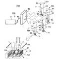
- the information processing system 100Aincludes a reader / writer 50A, a plurality of communication terminals 60A, and a wireless IC tag 1A.
- the reader / writer 50 ⁇ / b> Aincludes a main body 51 including an information processing circuit and the like, and an electric field antenna 53 connected to the main body 51 through a signal line 52.
- the communication terminal 60Afunctions as a pen-type reader / writer, and includes a first antenna unit 61, a second antenna unit 62, and a connection unit 63 that electrically connects both of these components.
- the second antenna portion 62is housed in the cylindrical housing 64 and is disposed at the tip of the housing 64.
- the first antenna unit 61is an electric field type dipole antenna, and is coupled to the antenna 53 of the reader / writer 50A by an electric field.
- the second antenna unit 62is a magnetic field type loop antenna and is coupled to the coiled antennas 20A and 20B of the wireless IC tag 1A by a magnetic field as will be described in detail below.
- the second antenna unit 62has a loop shape having an area substantially equal to the area of the antennas 20A and 20B of the wireless IC tag 1A.
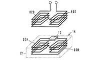
- the wireless IC tag 1Aincludes a wireless IC chip 10 that processes a transmission / reception signal of a predetermined frequency, and two coiled antennas 20A and 20B.
- the wireless IC chip 10includes a clock circuit, a logic circuit, a memory circuit, etc., stores necessary information, and has a pair of input / output terminal electrodes (not shown) on the back surface.
- the coiled antennas 20A and 20Bare obtained by winding a conductor in a coil shape, and one end of each is electrically connected to the input / output terminal electrode of the wireless IC chip 10 and the other end is electrically connected to each other. ing. These antennas 20A and 20B have their winding axes arranged at different positions in plan view and have the same winding direction. As described below with reference to FIG. 2, the antennas 20 ⁇ / b> A and 20 ⁇ / b> B are configured by stacking a plurality of coil conductors formed on the substrate 21, and the wireless IC chip 10 is mounted on the substrate 21.
- a high frequency (HF band, UHF band or higher frequency band) radiated from the antenna 53 of the reader / writer 50Ais received by the first antenna unit 61 of the communication terminal 60A, and the connection unit 63 is connected. Via the second antenna unit 62. And the magnetic flux based on the signal of the predetermined frequency radiated
- a response signal from the radio IC chip 10is radiated from the coiled antennas 20A and 20B to the second antenna unit 62, and the signal is supplied to the first antenna unit 61 through the connection unit 63, and the antenna of the reader / writer 50A is supplied. 53 is received and read by the main body 51.
- each of the first antenna 61 and the second antenna unit 62handles signals used in one information processing system 100A such as a UHF band RFID system, and the communication terminal 60A is a reader. Since the intermediation is performed between the writer 50A and the wireless IC tag 1A, communication is possible even if the reader / writer 50A and the wireless IC tag 1A are arranged at a distance that cannot be communicated alone. In particular, since the antenna 53 of the reader / writer 50A and the first antenna unit 61 of the communication terminal 60A are coupled by an electric field, communication over a relatively long distance is possible. Moreover, the existing electric field type can be used for the antenna 53 of the reader / writer 50A.
- the antennas 20A and 20B of the wireless IC tag 1A and the second antenna unit 62are coupled by a magnetic field, the magnetic field is attenuated more than the electric field, and communication is performed at a short distance. Even if 1A exists, a specific tag 1A can be reliably read. Further, since the communication terminal 60A is wirelessly coupled to the reader / writer 50A, a plurality of wireless IC tags 1A can be read simultaneously using the plurality of communication terminals 60A.
- the connection between the first antenna unit 61 and the second antenna unit 62is DC-connected by the connection unit 63, so that signals can be transmitted efficiently.
- the connection between themmay be a wireless connection such as electromagnetic coupling.
- the communication terminal 60Aincludes antenna units 61 and 62 and a connection unit 63, and does not require a driving power source such as a battery, its peripheral circuit, or a wireless communication device such as Bluetooth (trademark).
- the communication terminal 60Acan be made small and inexpensive.
- the second antenna unit 62is disposed at the tip of the housing 64, it is easy to couple the first antenna unit 61 and the second antenna unit 62 together.
- the communication terminal 60Ais a pen type, holds the housing 64 by hand, and communicates with the wireless IC chip 10 in proximity to the wireless IC tag 1A to be read.
- the human bodymay also function as an antenna that couples with an electric field. Therefore, when the first antenna unit 61 is arranged at a portion gripped with a finger, the human body also acts as an antenna, and the sensitivity of the first antenna unit 61 is improved.
- the housing 64which is a pen type of the communication terminal 60A, may be configured as an article having an actual function in addition to simply having a function as a communication terminal of the RFID system.
- the communication terminal 60Aitself may be a ballpoint pen or a mobile phone.
- the wireless IC tag 1Asince the coiled antennas 20A and 20B have the same winding direction, currents generated in the antennas 20A and 20B do not cancel each other, and energy transmission efficiency is improved. That is, the communication distance between the second antenna unit 62 and the antennas 20A and 20B is increased. Further, the antennas 20A and 20B are formed in a laminated structure, and the coil conductors are formed at positions overlapping each other in plan view, so that the opening area of the coil can be increased and the crossing magnetic flux increases, so that the communication distance Increases more.
- the imaginary part of the impedance of the wireless IC chip 10 and the imaginary part of the impedance of the coiled antennas 20A and 20Bhave a conjugate relationship with the frequency of the signal used for communication. That is, it is desirable that the resonance frequencies of the coiled antennas 20A and 20B are in the vicinity of the use frequency. It is further desirable that the real parts of the impedance match.
- the wireless IC tag 1Acan be summarized into, for example, a size of 3.2 mm in length, 1.6 mm in width, and 0.5 mm in height.
- the substrate 21is formed by stacking electrodes, conductors, and via-hole conductors on a plurality of sheets. Electrodes 31a and 31b connected to the input / output terminal electrodes of the wireless IC chip 10 are formed in the first layer, and coil conductors 32a, 32b, 33a, 33b, 34a, and the like are formed in the second to fourth layers. 34b is formed, and the connecting coil conductor 35 is formed in the fifth layer.
- the coil conductors 32a, 32b to 34a, 34bare connected in a coil shape via via-hole conductors 36a, 36b to form antennas 20A, 20B, and the other ends of both ends of the coil conductor 35 via via-hole conductors 37a, 37b. It is connected to the. Further, one ends of the antennas 20A and 20B are connected to the electrodes 31a and 31b via via-hole conductors 38a and 38b.
- Each sheet of the substrate 21may be formed of a general resin having a dielectric constant of 3 to 4, but is preferably formed of a material having a higher dielectric constant.
- the stability of operationcan be achieved in addition to increasing the opening. That is, since the capacitance between the coil conductors is determined by the material (sheet material) between the coil conductors, the influence of the dielectric constant of the article to which the wireless IC tag 1A is attached is small (floating capacitance is less likely to fluctuate), and the coil There is little change in the inductance value. Therefore, the change in the resonance frequency is small and the communication distance is stabilized.
- the impedance of the coil in the substrate 21is substantially determined, and the substrate 21 is less affected by the use environment.
- the second antenna portion of the communication terminalcan be modified into various shapes, and modifications 1 to 4 are shown below.
- the second antenna portionmay not be a loop shape but may be electric field type antennas 62A and 62B having a flat plate shape as shown in FIG. Since the coiled antennas 20A and 20B of the wireless IC tag 1A are divided into two, an electric field is generated by generating a potential difference between the antennas 20A and 20B. Therefore, even the antennas 62A and 62B having the electric field type flat plate shape can be operated. Note that when the electric field type antennas 62A and 62B are used as the second antenna portion, the antenna of the wireless IC tag may be an electric field type.
- the second antenna sectionmay be a multi-turn loop-shaped magnetic field type antenna 62C as shown in FIG. Since the strength of the magnetic field is increased, the communication distance can be increased.
- the second antenna unitmay be composed of a first coiled antenna unit 62D and a second coiled antenna unit 62E, similar to the coiled antennas 20A and 20B.
- One end of each of the coiled antenna portions 62D and 62Eis electrically connected to the first antenna portion 61 via the connection portion 63, and the other end is electrically connected to each other.
- antenna part 62D, 62Eis arrange
- the coiled antenna portions 62D and 62Ehave the same winding direction, the same effects as the coiled antennas 20A and 20B are obtained, and the energy transmission efficiency during communication with the wireless IC tag 1A is improved.
- the communication distancecan be increased. It also contributes to the downsizing of the communication terminal 60A.
- a matching circuit including inductances L ⁇ b> 1 and L ⁇ b> 2 and a capacitance Cmay be provided in the connection portion 63 (that is, between the second antenna portion 62 and the first antenna portion 61). Since impedance matching at the operating frequency can be achieved, the energy transfer efficiency between the first antenna unit 61 and the second antenna unit 62 is improved, and the communication distance can be increased even with a small amount of power.
- the matching circuitmay have a circuit configuration other than that shown in FIG.
- the wireless IC tag 1B shown in FIG. 7is formed by forming external electrodes 23A and 23B facing the antennas 20A and 20B on the surface (lower surface) of the substrate 21 in which the antennas 20A and 20B are built. Other configurations are the same as those of the wireless IC tag 1A. By providing the external electrodes 23A and 23B, the wireless IC tag 1B can be soldered to an article such as a printed wiring board.
- the wireless IC tag 1Bmay connect meandering boost antennas 24A and 24B to the external electrodes 23A and 23B.
- the boost antennas 24A and 24Bare a field emission type, but may be a loop-shaped magnetic field emission type boost antenna.
- a wireless IC tag 1C shown in FIG. 9Ais obtained by electrically connecting external electrodes 23A and 23B provided on the wireless IC tag 1B to coiled antennas 20A and 20B. Further, as shown in FIG. 9B, capacitors C1 and C2 may be interposed between the external electrodes 23A and 23B and the coiled antennas 20A and 20B.
- the relationship between the potentials of bothcan be easily determined, and the impedance of the external electrodes 23A and 23B can be determined. It can be easily designed to various values.
- the external electrodes 23A and 23Bwhen connected via the capacitors C1 and C2, the external electrodes 23A and 23B are not directly connected to the wireless IC chip 10, so that the wireless IC chip 10 is resistant to intrusion of static electricity. Can be protected.
- the antenna of the wireless IC tagis not two coiled antennas, but may be, for example, one coiled antenna 20C of one turn as shown in FIG. As shown in FIG. 11, a single coiled antenna 20D having a plurality of turns may be used.
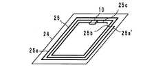
- a coiled antenna 25 formed on the front and back surfaces of one film 24may be used. That is, a coil conductor 25 a wound a plurality of times is formed on the surface of the film 24, its end 25 a ′ is exposed on the back surface of the film 24 and connected to the coil conductor 25 b, and the coil conductor 25 b is connected to the film 24. It may be exposed on the surface and connected to the coil conductor 25c.
- the antennas 20A and 20B of the wireless IC tagmay not be shown, but may have different numbers of windings, or may have different sizes.
- the number of coiled antennasmay be three or more.
- another coiled antennamay be interposed between the coiled antennas 20A and 20B.
- the connecting portion 63may be covered with a ferrite material 65 as shown in FIG.
- the line of the connecting portion 63 and other ground conductorsbecome a part of the electric field antenna and may affect the radiation characteristics.
- the connection portion 63By covering the connection portion 63 with the ferrite material 65, the first antenna portion 61 and the second antenna portion 62 can be separated, and the electric field type first antenna portion 61 can have a radiation characteristic as designed. it can.
- the first antenna unit 61may be an electric field type monopole antenna.
- the lower half of the first antenna portion 61is configured as a coaxial line covered with a cylindrical ground electrode 68, and one end of the loop-shaped second antenna portion 62 is connected to the lower end of the first antenna portion 61, The other end is connected to the ground electrode 68.
- the communication terminal 60Acan be configured to be thin and simple, and the manufacturing cost can be reduced. Further, since the lower half is covered with the ground electrode 68, the change in characteristics as an antenna is small even if the lower half is held by hand.
- the information processing system 100Bincludes a reader / writer 50B having a magnetic field type loop antenna 54, and a communication terminal 60B having a first antenna unit as a magnetic field type loop antenna 61B. And the wireless IC tag 1A.
- Other configurationsare the same as those of the information processing system 100A, and the effects thereof are also the same.
- the information processing system 100Bcan be operated even when the reader / writer antenna is a magnetic field type.
- the antenna 55 of the reader / writer 50Ais housed in the holder 56 as a small electric field type, and the antenna 55 communicates.
- the terminal 60 ⁇ / b> Ccan be inserted adjacent to the first antenna unit 61 into the housing 64.
- FIG. 16Aby attaching the antenna 55 to the communication terminal 60C, reliable communication is possible in a state where the antenna 55 and the first antenna unit 61 are close to each other.
- FIG. 16Bby taking out the antenna 55 from the communication terminal 60C, it is possible to perform communication at a distant place as in the information processing system 100A.
- the reader / writer 50 and the communication terminal 60 ⁇ / b> Cmay be integrated by reducing the size of the main body 51 of the reader / writer 50 and storing it in the holder 56 or by attaching it to the housing 64.
- an information processing system 100Dhas a receptor 66 in which a connector 57 is connected to the tip of a signal line 52 of a reader / writer 50A, and the connector 57 is connected to an extension portion of a connection portion 63. It is designed to be detachable. By connecting the connector 57 to the receptor 66, the reader / writer 50 ⁇ / b> A and the communication terminal 60 ⁇ / b> A can be connected by wire, and stable communication is possible.
- the communication terminal and the information processing system according to the present inventionare not limited to the above-described embodiments, and can be variously modified within the scope of the gist thereof.
- the wireless IC chipis mounted on the substrate on which the antenna is formed, but the wireless IC chip may be mounted in the substrate.
- An antennamay be formed in the rewiring layer of the wireless IC chip.
- the information processing system targeted by the communication terminalis not limited to the UHF band RFID system, and may be another communication system such as an HF band RFID system.
- the present inventionis useful for communication terminals and information processing systems, and is particularly excellent in that the communication distance between a reader / writer and a wireless IC tag can be increased.
- 1A, 1B, 1C ... wireless IC tag 10... wireless IC chip 50A, 50B ... reader / writer 53, 54, 55 ... antenna 60A, 60B, 60C ... communication terminal 61, 61B ... first antenna portion 62 ... second antenna portion 63 ... Connection part 64 ... Housing 65 ... Ferrite material 100A, 100B, 100C, 100D ... Information processing system
Landscapes
- Near-Field Transmission Systems (AREA)
- Details Of Aerials (AREA)
- Variable-Direction Aerials And Aerial Arrays (AREA)
Abstract
Description
本発明は、通信端末、特に、RFID(Radio Frequency Identification)システムに用いることのできる通信端末、及び、該通信端末を備えた情報処理システムに関する。The present invention relates to a communication terminal, in particular, a communication terminal that can be used in an RFID (Radio Frequency Identification) system, and an information processing system including the communication terminal.
従来、物品の管理システムとして、誘導電磁界を発生するリーダライタと物品に付された所定の情報を記憶した無線タグとを非接触方式で通信し、情報を伝達するRFIDシステムが開発されている。この種のRFIDシステムの一例として、特許文献1には、入力ペンの内部にRFID装置(無線ICタグ)を内蔵させ、該RFID装置と情報処理装置(リーダライタ)とが通信可能な範囲にある場合に、情報処理装置がRFID装置の情報を読み出し、ペン使用者の認識あるいはペンによって書かれた文字認識を行う情報処理システムが記載されている。2. Description of the Related Art Conventionally, as an article management system, an RFID system has been developed that communicates information in a contactless manner between a reader / writer that generates an induction electromagnetic field and a wireless tag that stores predetermined information attached to the article. . As an example of this type of RFID system,Patent Document 1 includes an RFID device (wireless IC tag) built in an input pen, and is within a range where the RFID device and an information processing device (reader / writer) can communicate. In this case, an information processing system is described in which an information processing device reads information from an RFID device and recognizes a pen user or a character written by a pen.
しかしながら、前記情報処理システムでは、RFID装置(無線ICタグ)とリーダライタとが通信可能な範囲にあることが動作条件であり、HF帯やUHF帯の高周波では通信距離が短いため、ごく近距離でしか通信ができないという問題点を生じている。However, in the information processing system, the operating condition is that the RFID device (wireless IC tag) and the reader / writer are in a communicable range, and the communication distance is short at a high frequency in the HF band and the UHF band, so that the distance is very short. There is a problem that communication is possible only with.
また、特許文献2には、書店における在庫管理のために親機と通信する複数のハンディー端末を有する在庫管理システムが記載されている。しかし、このハンディー端末は、バッテリーや信号処理回路を内蔵したものであり、構成が複雑で、大型であるという問題点を有している。Further, Patent Document 2 describes an inventory management system having a plurality of handy terminals that communicate with a master unit for inventory management in a bookstore. However, this handy terminal incorporates a battery and a signal processing circuit, and has a problem that its configuration is complicated and large.
そこで、本発明の目的は、簡易な構成でリーダライタと無線ICタグとの通信距離を長くすることのできる通信端末及び情報処理システムを提供することにある。Therefore, an object of the present invention is to provide a communication terminal and an information processing system that can increase the communication distance between a reader / writer and a wireless IC tag with a simple configuration.
前記目的を達成するため、本発明の第1の形態である通信端末は、
第1アンテナ部と、第2アンテナ部と、前記第1アンテナ部と前記第2アンテナ部とを電気的に接続する接続部と、を備え、
前記第1アンテナ部及び前記第2アンテナ部はそれぞれ一の情報処理システムで使用する信号を扱うものであり、
前記第1アンテナ部で受信した信号を前記第2アンテナ部から送信し、前記第2アンテナ部で受信した信号を前記第1アンテナ部から送信すること、
を特徴とする。In order to achieve the above object, a communication terminal according to the first aspect of the present invention provides:
A first antenna unit, a second antenna unit, and a connection unit that electrically connects the first antenna unit and the second antenna unit;
Each of the first antenna unit and the second antenna unit handles signals used in one information processing system,
Transmitting a signal received by the first antenna unit from the second antenna unit, and transmitting a signal received by the second antenna unit from the first antenna unit;
It is characterized by.
本発明の第2の形態である情報処理システムは、
リーダライタと、通信端末と、無線ICタグと、を備え、
前記通信端末は、第1アンテナ部と、第2アンテナ部と、前記第1アンテナ部と前記第2アンテナ部とを電気的に接続する接続部と、を備え、
前記第1アンテナ部が前記リーダライタと通信し、
前記第2アンテナ部が前記無線ICタグと通信し、
前記無線ICタグに格納されている情報を前記リーダライタで読み取ること、
を特徴とする。An information processing system according to the second aspect of the present invention is
A reader / writer, a communication terminal, and a wireless IC tag,
The communication terminal includes a first antenna unit, a second antenna unit, and a connection unit that electrically connects the first antenna unit and the second antenna unit,
The first antenna unit communicates with the reader / writer;
The second antenna unit communicates with the wireless IC tag;
Reading information stored in the wireless IC tag with the reader / writer;
It is characterized by.
前記通信端末は、第1アンテナ部と第2アンテナ部とが互いに電気的に接続されており、第1アンテナ部がリーダライタと通信し、第2アンテナ部が無線ICタグと通信する。即ち、通信端末がリーダライタと無線ICタグとの間を仲介するため、リーダライタと無線ICタグとがそれのみでは通信不能な離れた距離に配置されていても通信が可能になる。また、通信端末はバッテリーや情報処理回路が不要であり、簡易に構成することができる。In the communication terminal, the first antenna unit and the second antenna unit are electrically connected to each other, the first antenna unit communicates with the reader / writer, and the second antenna unit communicates with the wireless IC tag. In other words, since the communication terminal mediates between the reader / writer and the wireless IC tag, communication is possible even if the reader / writer and the wireless IC tag are arranged at a distance that cannot be communicated alone. Further, the communication terminal does not require a battery or an information processing circuit, and can be configured simply.
本発明によれば、通信端末が無線ICタグとリーダライタとの間を仲介するため、通信距離を長くすることができる。According to the present invention, since the communication terminal mediates between the wireless IC tag and the reader / writer, the communication distance can be increased.
以下に、本発明に係る通信端末及び情報処理システムの実施例について添付図面を参照して説明する。なお、各図において、同一の部品、部分には共通する符号を付し、重複する説明は省略する。Embodiments of a communication terminal and an information processing system according to the present invention will be described below with reference to the accompanying drawings. In addition, in each figure, the same code | symbol is attached | subjected to the same components and parts, and the overlapping description is abbreviate | omitted.
(第1実施例、図1及び図2参照)
第1実施例である情報処理システム100Aは、図1に示すように、リーダライタ50Aと、複数の通信端末60Aと、無線ICタグ1Aとで構成されている。リーダライタ50Aは、情報処理回路などを含む本体51と、該本体51と信号線52で接続された電界型アンテナ53とを備えている。(Refer to the first embodiment, FIGS. 1 and 2)
As shown in FIG. 1, theinformation processing system 100A according to the first embodiment includes a reader /writer 50A, a plurality ofcommunication terminals 60A, and awireless IC tag 1A. The reader / writer 50 </ b> A includes amain body 51 including an information processing circuit and the like, and anelectric field antenna 53 connected to themain body 51 through asignal line 52.
第1実施例である情報処理システム100Aは、図1に示すように、リーダライタ50Aと、複数の通信端末60Aと、無線ICタグ1Aとで構成されている。リーダライタ50Aは、情報処理回路などを含む本体51と、該本体51と信号線52で接続された電界型アンテナ53とを備えている。(Refer to the first embodiment, FIGS. 1 and 2)
As shown in FIG. 1, the
通信端末60Aは、ペン型のリーダライタとして機能するものであり、第1アンテナ部61と、第2アンテナ部62と、この両者を電気的に接続する接続部63とを備え、これらの部品は筒状の筺体64に収容され、第2アンテナ部62は筺体64の先端部に配置されている。第1アンテナ部61は、電界型のダイポールアンテナであり、リーダライタ50Aのアンテナ53と電界によって結合する。第2アンテナ部62は、磁界型のループアンテナであり、以下に詳述するように無線ICタグ1Aのコイル状アンテナ20A,20Bと磁界によって結合する。第2アンテナ部62は無線ICタグ1Aのアンテナ20A,20Bを合わせた面積とほぼ等しい面積のループ形状をなしている。Thecommunication terminal 60A functions as a pen-type reader / writer, and includes afirst antenna unit 61, asecond antenna unit 62, and aconnection unit 63 that electrically connects both of these components. Thesecond antenna portion 62 is housed in thecylindrical housing 64 and is disposed at the tip of thehousing 64. Thefirst antenna unit 61 is an electric field type dipole antenna, and is coupled to theantenna 53 of the reader /writer 50A by an electric field. Thesecond antenna unit 62 is a magnetic field type loop antenna and is coupled to the coiledantennas wireless IC tag 1A by a magnetic field as will be described in detail below. Thesecond antenna unit 62 has a loop shape having an area substantially equal to the area of theantennas wireless IC tag 1A.
無線ICタグ1Aは、所定周波数の送受信信号を処理する無線ICチップ10と、二つのコイル状アンテナ20A,20Bと、を備えている。無線ICチップ10は、クロック回路、ロジック回路、メモリ回路などを含み、必要な情報がメモリされており、裏面に図示しない一対の入出力端子電極が設けられている。Thewireless IC tag 1A includes awireless IC chip 10 that processes a transmission / reception signal of a predetermined frequency, and two coiledantennas wireless IC chip 10 includes a clock circuit, a logic circuit, a memory circuit, etc., stores necessary information, and has a pair of input / output terminal electrodes (not shown) on the back surface.
コイル状アンテナ20A,20Bは、導体をコイル状に巻回したもので、それぞれの一端は無線ICチップ10の入出力端子電極に電気的に接続され、それぞれの他端は互いに電気的に接続されている。これらのアンテナ20A,20Bはそれぞれの巻回軸が平面視で異なる位置に配置され、かつ、巻回方向が同じである。アンテナ20A,20Bは、図2を参照して以下に説明するように、基板21に形成されたコイル導体を複数積層して構成され、無線ICチップ10は基板21上に実装されている。The coiledantennas wireless IC chip 10 and the other end is electrically connected to each other. ing. Theseantennas antennas 20 </ b> A and 20 </ b> B are configured by stacking a plurality of coil conductors formed on thesubstrate 21, and thewireless IC chip 10 is mounted on thesubstrate 21.
この情報処理システム100Aにおいて、リーダライタ50Aのアンテナ53から放射された高周波(HF帯、UHF帯あるいはそれ以上の高周波数帯)が通信端末60Aの第1アンテナ部61で受信され、接続部63を介して第2アンテナ部62に伝達される。そして、筺体64の先端部に配置された第2アンテナ部62を無線ICタグ1Aに近接させることによって、第2アンテナ部62から放射された所定周波数の信号に基づく磁束がコイル状アンテナ20A,20Bを貫通することにより、該アンテナ20A,20Bに電流が流れる。即ち、第2アンテナ部62とアンテナ20A,20Bが電磁結合する。この電流が無線ICチップ10に供給されて無線ICチップ10を動作させる。In thisinformation processing system 100A, a high frequency (HF band, UHF band or higher frequency band) radiated from theantenna 53 of the reader /writer 50A is received by thefirst antenna unit 61 of thecommunication terminal 60A, and theconnection unit 63 is connected. Via thesecond antenna unit 62. And the magnetic flux based on the signal of the predetermined frequency radiated | emitted from the2nd antenna part 62 by making the2nd antenna part 62 arrange | positioned at the front-end | tip part of the housing |casing 64 close to thewireless IC tag 1A causes thecoiled antennas antennas second antenna unit 62 and theantennas wireless IC chip 10 to operate thewireless IC chip 10.
一方、無線ICチップ10からの応答信号がコイル状アンテナ20A,20Bから第2アンテナ部62に放射され、その信号は接続部63を介して第1アンテナ部61に供給され、リーダライタ50Aのアンテナ53で受信されて本体51で読み取られる。On the other hand, a response signal from theradio IC chip 10 is radiated from the coiledantennas second antenna unit 62, and the signal is supplied to thefirst antenna unit 61 through theconnection unit 63, and the antenna of the reader /writer 50A is supplied. 53 is received and read by themain body 51.
即ち、本第1実施例において、第1アンテナ61及び第2アンテナ部62はそれぞれ例えばUHF帯RFIDシステムのような一の情報処理システム100Aで使用する信号を扱うものであり、通信端末60Aがリーダライタ50Aと無線ICタグ1Aとの間を仲介するため、リーダライタ50Aと無線ICタグ1Aとがそれのみでは通信不能な離れた距離に配置されていても通信が可能になる。特に、リーダライタ50Aのアンテナ53と通信端末60Aの第1アンテナ部61とが電界によって結合するため、比較的長い距離での通信が可能である。しかも、リーダライタ50Aのアンテナ53は既存の電界型を使用できる。また、無線ICタグ1Aのアンテナ20A,20Bと第2アンテナ部62とは磁界によって結合するため、磁界は電界よりも減衰が大きく、近距離で通信が行われることになり、複数の無線ICタグ1Aが存在していても特定のタグ1Aを確実に読み取ることが可能である。また、通信端末60Aがリーダライタ50Aと無線で結合しているため、複数の通信端末60Aを用いて複数の無線ICタグ1Aを同時に読み取ることができる。That is, in the first embodiment, each of thefirst antenna 61 and thesecond antenna unit 62 handles signals used in oneinformation processing system 100A such as a UHF band RFID system, and thecommunication terminal 60A is a reader. Since the intermediation is performed between thewriter 50A and thewireless IC tag 1A, communication is possible even if the reader /writer 50A and thewireless IC tag 1A are arranged at a distance that cannot be communicated alone. In particular, since theantenna 53 of the reader /writer 50A and thefirst antenna unit 61 of thecommunication terminal 60A are coupled by an electric field, communication over a relatively long distance is possible. Moreover, the existing electric field type can be used for theantenna 53 of the reader /writer 50A. In addition, since theantennas wireless IC tag 1A and thesecond antenna unit 62 are coupled by a magnetic field, the magnetic field is attenuated more than the electric field, and communication is performed at a short distance. Even if 1A exists, aspecific tag 1A can be reliably read. Further, since thecommunication terminal 60A is wirelessly coupled to the reader /writer 50A, a plurality ofwireless IC tags 1A can be read simultaneously using the plurality ofcommunication terminals 60A.
第1アンテナ部61と第2アンテナ部62との接続は、接続部63によって直流接続されており、効率よく信号を伝達することができる。但し、両者の接続は電磁界結合のような無線接続であってもよい。また、通信端末60Aはアンテナ部61,62と接続部63にて構成されており、バッテリーのような駆動用電源やその周辺回路、さらにはブルートゥース(商標)のような無線通信機を必要とせず、通信端末60Aを小型・安価にできる。さらに、筐体64の先端部に第2アンテナ部62を配置しているため、第1アンテナ部61と第2アンテナ部62とを結合させることが容易である。The connection between thefirst antenna unit 61 and thesecond antenna unit 62 is DC-connected by theconnection unit 63, so that signals can be transmitted efficiently. However, the connection between them may be a wireless connection such as electromagnetic coupling. Thecommunication terminal 60A includesantenna units connection unit 63, and does not require a driving power source such as a battery, its peripheral circuit, or a wireless communication device such as Bluetooth (trademark). Thecommunication terminal 60A can be made small and inexpensive. Furthermore, since thesecond antenna unit 62 is disposed at the tip of thehousing 64, it is easy to couple thefirst antenna unit 61 and thesecond antenna unit 62 together.
通信端末60Aはペンタイプであり、筺体64を手で保持して読取り対象となる無線ICタグ1Aに近接させて無線ICチップ10と通信する。人体も電界と結合するアンテナとして機能することがある。従って、第1アンテナ部61を指で握る部分に配置すると人体もアンテナとして作用し、第1アンテナ部61の感度が向上する。Thecommunication terminal 60A is a pen type, holds thehousing 64 by hand, and communicates with thewireless IC chip 10 in proximity to thewireless IC tag 1A to be read. The human body may also function as an antenna that couples with an electric field. Therefore, when thefirst antenna unit 61 is arranged at a portion gripped with a finger, the human body also acts as an antenna, and the sensitivity of thefirst antenna unit 61 is improved.
通信端末60Aのペンタイプである筺体64は、単にRFIDシステムの通信端末としての機能を有する以外に、実際上の機能を有する物品として構成されていてもよい。例えば、通信端末60A自体がボールペンであったり、携帯電話機であってもよい。Thehousing 64, which is a pen type of thecommunication terminal 60A, may be configured as an article having an actual function in addition to simply having a function as a communication terminal of the RFID system. For example, thecommunication terminal 60A itself may be a ballpoint pen or a mobile phone.
無線ICタグ1Aに関しては、コイル状アンテナ20A,20Bは互いの巻回方向が同じであるため、各アンテナ20A,20Bに生じた電流が打ち消し合うことはなく、エネルギー伝達効率が向上する。即ち、第2アンテナ部62とアンテナ20A,20Bとの通信距離が長くなる。また、アンテナ20A,20Bを積層構造で形成し、それぞれのコイル導体を平面視で重なる位置に形成することにより、コイルの開口面積を大きくすることができ、交差する磁束が多くなるため、通信距離がより増加する。Regarding thewireless IC tag 1A, since thecoiled antennas antennas second antenna unit 62 and theantennas antennas
無線ICチップ10のインピーダンスの虚数部と、コイル状アンテナ20A,20Bのインピーダンスの虚数部は、通信に使用する信号の周波数で共役の関係になるようにすることが望ましい。つまり、コイル状アンテナ20A,20Bの共振周波数が使用周波数付近にあることが望ましい。インピーダンスの実部が一致することはさらに望ましい。It is desirable that the imaginary part of the impedance of thewireless IC chip 10 and the imaginary part of the impedance of thecoiled antennas coiled antennas
特に、コイル状アンテナ20A,20Bを積層タイプで大きな開口部とすると、小型で大きいインダクタンス値を得ることができ、ひいては、無線ICタグ1A自体が小型化される。使用周波数を950MHz近辺の短波長とすることで、より小型になる。通信にUHF帯の周波数を用いる場合、無線ICタグ1Aとしては、例えば、縦3.2mm、横1.6mm、高さ0.5mmのサイズにまとめることができる。Particularly, if thecoiled antennas wireless IC tag 1A itself can be downsized. By making the operating frequency a short wavelength around 950 MHz, the size is further reduced. In the case of using a UHF band frequency for communication, thewireless IC tag 1A can be summarized into, for example, a size of 3.2 mm in length, 1.6 mm in width, and 0.5 mm in height.
ここで、コイル状アンテナ20A,20Bの積層構造の一例を図2を参照して説明する。基板21は複数枚のシートに電極や導体、ビアホール導体を形成して積層したものである。第1層目には無線ICチップ10の入出力端子電極に接続される電極31a,31bが形成され、第2層目から第4層目にはコイル導体32a,32b,33a,33b,34a,34bが形成され、第5層目には接続用コイル導体35が形成されている。コイル導体32a,32b~34a,34bはビアホール導体36a,36bを介してコイル状に接続してアンテナ20A,20Bを形成し、それぞれの他端はビアホール導体37a,37bを介してコイル導体35の両端に接続されている。また、アンテナ20A,20Bの一端はビアホール導体38a,38bを介して電極31a,31bに接続されている。Here, an example of a laminated structure of thecoiled antennas substrate 21 is formed by stacking electrodes, conductors, and via-hole conductors on a plurality of sheets.Electrodes 31a and 31b connected to the input / output terminal electrodes of thewireless IC chip 10 are formed in the first layer, andcoil conductors coil conductor 35 is formed in the fifth layer. Thecoil conductors 32a, 32b to 34a, 34b are connected in a coil shape via via-hole conductors 36a, 36b to formantennas coil conductor 35 via via-hole conductors 37a, 37b. It is connected to the. Further, one ends of theantennas electrodes 31a and 31b via via-hole conductors 38a and 38b.
基板21の各シートは、一般的な誘電率3~4の樹脂で形成してもよいが、それよりも高い誘電率の材料で形成することが好ましい。例えば、誘電率が7以上のセラミックである。Each sheet of thesubstrate 21 may be formed of a general resin having a dielectric constant of 3 to 4, but is preferably formed of a material having a higher dielectric constant. For example, a ceramic having a dielectric constant of 7 or more.
コイル状アンテナ20A,20Bを積層タイプとすることで、開口部を大きくできる以外に、動作の安定性を図ることができる。即ち、前記コイル導体間の容量がコイル導体間の材質(シートの材質)によって決まるため、無線ICタグ1Aの貼着対象物品の誘電率の影響が少なく(浮遊容量の変動が生じにくい)、コイルのインダクタンス値の変化が少ない。それゆえ、共振周波数の変化が少なく、通信距離が安定することになる。特に、基板21に高誘電率の材料を用いることで、基板21内でのコイルのインピーダンスがほぼ決定され、使用環境からの影響を受けにくくなる。By making thecoiled antennas wireless IC tag 1A is attached is small (floating capacitance is less likely to fluctuate), and the coil There is little change in the inductance value. Therefore, the change in the resonance frequency is small and the communication distance is stabilized. In particular, by using a high dielectric constant material for thesubstrate 21, the impedance of the coil in thesubstrate 21 is substantially determined, and thesubstrate 21 is less affected by the use environment.
(第2アンテナ部の各種変形例、図3~図6参照)
通信端末の第2アンテナ部は種々の形状に変形することができ、以下にその変形例1~4を示す。まず、第2アンテナ部は、ループ形状ではなく、図3に示すように、平板状をなす電界型のアンテナ62A,62Bであってもよい。無線ICタグ1Aのコイル状アンテナ20A,20Bは二つに分かれているため、それぞれのアンテナ20A,20Bで電位差を生じて電界が発生する。このため、電界型の平板状をなすアンテナ62A,62Bであっても動作させることができる。なお、第2のアンテナ部として電界型のアンテナ62A,62Bを用いる場合、無線ICタグのアンテナを電界型としてもよい。(Refer to FIGS. 3 to 6 for various modifications of the second antenna section.)
The second antenna portion of the communication terminal can be modified into various shapes, andmodifications 1 to 4 are shown below. First, the second antenna portion may not be a loop shape but may be electricfield type antennas coiled antennas wireless IC tag 1A are divided into two, an electric field is generated by generating a potential difference between theantennas antennas field type antennas
通信端末の第2アンテナ部は種々の形状に変形することができ、以下にその変形例1~4を示す。まず、第2アンテナ部は、ループ形状ではなく、図3に示すように、平板状をなす電界型のアンテナ62A,62Bであってもよい。無線ICタグ1Aのコイル状アンテナ20A,20Bは二つに分かれているため、それぞれのアンテナ20A,20Bで電位差を生じて電界が発生する。このため、電界型の平板状をなすアンテナ62A,62Bであっても動作させることができる。なお、第2のアンテナ部として電界型のアンテナ62A,62Bを用いる場合、無線ICタグのアンテナを電界型としてもよい。(Refer to FIGS. 3 to 6 for various modifications of the second antenna section.)
The second antenna portion of the communication terminal can be modified into various shapes, and
第2アンテナ部は、図4に示すように、複数ターンのループ形状の磁界型のアンテナ62Cであってもよい。磁界の強度が強まるため、通信距離を長くすることができる。The second antenna section may be a multi-turn loop-shaped magneticfield type antenna 62C as shown in FIG. Since the strength of the magnetic field is increased, the communication distance can be increased.
第2アンテナ部は、図5に示すように、前記コイル状アンテナ20A,20Bと同様に、第1のコイル状アンテナ部62D及び第2のコイル状アンテナ部62Eにて構成されていてもよい。コイル状アンテナ部62D,62Eのそれぞれの一端は接続部63を介して第1アンテナ部61と電気的に接続され、それぞれの他端は互いに電気的に接続されている。そして、アンテナ部62D,62Eはそれぞれの巻回軸が平面視で異なる位置に配置され、かつ、巻回方向が同じである。As shown in FIG. 5, the second antenna unit may be composed of a firstcoiled antenna unit 62D and a secondcoiled antenna unit 62E, similar to thecoiled antennas antenna portions first antenna portion 61 via theconnection portion 63, and the other end is electrically connected to each other. Andantenna part
このコイル状アンテナ部62D,62Eは、巻回方向が同じとされているため、前記コイル状アンテナ20A,20Bと同様の作用効果を奏し、無線ICタグ1Aとの通信時におけるエネルギー伝達効率を向上させ、通信距離を長くすることができる。また、通信端末60Aの小型化にも寄与する。なお、変形例3のアンテナ62D,62Eを用いる場合、無線ICタグとしては、必ずしも、二つのコイル状アンテナを用いる必要はない。Since the coiledantenna portions coiled antennas wireless IC tag 1A is improved. The communication distance can be increased. It also contributes to the downsizing of thecommunication terminal 60A. In addition, when using theantennas
図6に示すように、接続部63に(即ち、第2アンテナ部62と第1アンテナ部61との間に)、インダクタンスL1,L2とキャパシタンスCとからなる整合回路を設けてもよい。使用周波数でのインピーダンスの整合をとることができるので、第1アンテナ部61と第2アンテナ部62とのエネルギー伝達効率が向上し、小さな電力でも通信距離を長くすることができる。なお、整合回路としては、図6に示すもの以外の回路構成であってもよい。As shown in FIG. 6, a matching circuit including inductances L <b> 1 and L <b> 2 and a capacitance C may be provided in the connection portion 63 (that is, between thesecond antenna portion 62 and the first antenna portion 61). Since impedance matching at the operating frequency can be achieved, the energy transfer efficiency between thefirst antenna unit 61 and thesecond antenna unit 62 is improved, and the communication distance can be increased even with a small amount of power. The matching circuit may have a circuit configuration other than that shown in FIG.
(無線ICタグの各種変形例、図7~図12参照)
次に、無線ICタグの各種変形例について説明する。図7に示す無線ICタグ1Bは、アンテナ20A,20Bを内蔵した基板21の表面(下面)にアンテナ20A,20Bにそれぞれ対向する外部電極23A,23Bを形成したものである。他の構成は前記無線ICタグ1Aと同様である。外部電極23A,23Bを設けることで、無線ICタグ1Bをプリント配線基板などの物品にはんだ付けすることができる。(Variations of wireless IC tags, see FIGS. 7 to 12)
Next, various modifications of the wireless IC tag will be described. Thewireless IC tag 1B shown in FIG. 7 is formed by formingexternal electrodes antennas substrate 21 in which theantennas wireless IC tag 1A. By providing theexternal electrodes wireless IC tag 1B can be soldered to an article such as a printed wiring board.
次に、無線ICタグの各種変形例について説明する。図7に示す無線ICタグ1Bは、アンテナ20A,20Bを内蔵した基板21の表面(下面)にアンテナ20A,20Bにそれぞれ対向する外部電極23A,23Bを形成したものである。他の構成は前記無線ICタグ1Aと同様である。外部電極23A,23Bを設けることで、無線ICタグ1Bをプリント配線基板などの物品にはんだ付けすることができる。(Variations of wireless IC tags, see FIGS. 7 to 12)
Next, various modifications of the wireless IC tag will be described. The
また、無線ICタグ1Bは、図8に示すように、ミアンダ状のブーストアンテナ24A,24Bを外部電極23A,23Bに接続してもよい。ブーストアンテナ24A,24Bは電界放射型であるが、ループ形状の磁界放射型のブーストアンテナであってもよい。Further, as shown in FIG. 8, thewireless IC tag 1B may connectmeandering boost antennas external electrodes boost antennas
図9(A)に示す無線ICタグ1Cは、前記無線ICタグ1Bに設けた外部電極23A,23Bをコイル状アンテナ20A,20Bに電気的に接続したものである。また、図9(B)に示すように、外部電極23A,23Bとコイル状アンテナ20A,20Bとの間に容量C1,C2を介在させてもよい。Awireless IC tag 1C shown in FIG. 9A is obtained by electrically connectingexternal electrodes wireless IC tag 1B to coiledantennas external electrodes coiled antennas
図9(A)に示すように、外部電極23A,23Bをコイル状アンテナ20A,20Bと電気的に直結すると、両者の電位の関係を簡単に決めることができ、外部電極23A,23Bのインピーダンスを様々な値に容易に設計することができる。また、図9(B)に示すように、容量C1,C2を介して接続すると、外部電極23A,23Bは無線ICチップ10とは直結していないため、静電気の侵入に対して無線ICチップ10を保護することができる。As shown in FIG. 9A, when theexternal electrodes coiled antennas external electrodes external electrodes wireless IC chip 10, so that thewireless IC chip 10 is resistant to intrusion of static electricity. Can be protected.
また、無線ICタグのアンテナは二つのコイル状アンテナではなく、例えば、図10に示すように、1ターンの一つのコイル状アンテナ20Cであってもよい。図11に示すように複数ターンの一つのコイル状アンテナ20Dであってもよい。さらに、図12に示すように、1枚のフィルム24の表裏面に形成したコイル状アンテナ25であってもよい。即ち、フィルム24の表面に複数回に巻回されたコイル導体25aを形成し、その端部25a’をフィルム24の裏面に露出させてコイル導体25bに接続し、該コイル導体25bをフィルム24の表面に露出させてコイル導体25cに接続してもよい。Also, the antenna of the wireless IC tag is not two coiled antennas, but may be, for example, onecoiled antenna 20C of one turn as shown in FIG. As shown in FIG. 11, a singlecoiled antenna 20D having a plurality of turns may be used. Furthermore, as shown in FIG. 12, acoiled antenna 25 formed on the front and back surfaces of onefilm 24 may be used. That is, a coil conductor 25 a wound a plurality of times is formed on the surface of thefilm 24, its end 25 a ′ is exposed on the back surface of thefilm 24 and connected to thecoil conductor 25 b, and thecoil conductor 25 b is connected to thefilm 24. It may be exposed on the surface and connected to the coil conductor 25c.
なお、無線ICタグのアンテナ20A,20Bは、図示しないが、互いに巻回数を異ならせたものであってもよく、互いにサイズの異なるものであってもよい。また、コイル状アンテナの個数は3以上であってもよい。例えば、コイル状アンテナ20A,20Bの間にいま一つのコイル状アンテナを介在させてもよい。Note that theantennas coiled antennas
(通信端末の変形例1、図13参照)
前記通信端末60Aに関しては、図13に示すように、接続部63をフェライト材65によって被覆するようにしてもよい。接続部63の線路やその他のグランド導体は電界型アンテナの一部となり、放射特性に影響する場合がある。接続部63をフェライト材65で被覆することにより、第1アンテナ部61と第2アンテナ部62とを分離することができ、電界型の第1アンテナ部61を設計どおりの放射特性にすることができる。(Refer toModification 1 of Communication Terminal, FIG. 13)
With respect to thecommunication terminal 60A, the connectingportion 63 may be covered with aferrite material 65 as shown in FIG. The line of the connectingportion 63 and other ground conductors become a part of the electric field antenna and may affect the radiation characteristics. By covering theconnection portion 63 with theferrite material 65, thefirst antenna portion 61 and thesecond antenna portion 62 can be separated, and the electric field typefirst antenna portion 61 can have a radiation characteristic as designed. it can.
前記通信端末60Aに関しては、図13に示すように、接続部63をフェライト材65によって被覆するようにしてもよい。接続部63の線路やその他のグランド導体は電界型アンテナの一部となり、放射特性に影響する場合がある。接続部63をフェライト材65で被覆することにより、第1アンテナ部61と第2アンテナ部62とを分離することができ、電界型の第1アンテナ部61を設計どおりの放射特性にすることができる。(Refer to
With respect to the
(通信端末の変形例2、図14参照)
前記通信端末60Aに関しては、図14に示すように、第1アンテナ部61は電界型のモノポールアンテナであってもよい。第1アンテナ部61の下半分は円筒形のグランド電極68によって覆われた同軸線路として構成されており、ループ形状の第2アンテナ部62はその一端が第1アンテナ部61の下端に接続され、他端がグランド電極68に接続されている。(Refer to communication terminal modification 2 and FIG. 14)
Regarding thecommunication terminal 60A, as shown in FIG. 14, thefirst antenna unit 61 may be an electric field type monopole antenna. The lower half of thefirst antenna portion 61 is configured as a coaxial line covered with acylindrical ground electrode 68, and one end of the loop-shapedsecond antenna portion 62 is connected to the lower end of thefirst antenna portion 61, The other end is connected to theground electrode 68.
前記通信端末60Aに関しては、図14に示すように、第1アンテナ部61は電界型のモノポールアンテナであってもよい。第1アンテナ部61の下半分は円筒形のグランド電極68によって覆われた同軸線路として構成されており、ループ形状の第2アンテナ部62はその一端が第1アンテナ部61の下端に接続され、他端がグランド電極68に接続されている。(Refer to communication terminal modification 2 and FIG. 14)
Regarding the
モノポールアンテナは前記ダイポールアンテナとは異なって1本の導体によって形成されるため、通信端末60Aを細型かつシンプルに構成でき、製造コストを抑えることができる。また、下半分はグランド電極68で覆われているため、下半分を手で持ってもアンテナとしての特性の変化が小さい。Since the monopole antenna is formed of a single conductor unlike the dipole antenna, thecommunication terminal 60A can be configured to be thin and simple, and the manufacturing cost can be reduced. Further, since the lower half is covered with theground electrode 68, the change in characteristics as an antenna is small even if the lower half is held by hand.
(第2実施例、図15参照)
第2実施例である情報処理システム100Bは、図15に示すように、磁界型のループアンテナ54を備えたリーダライタ50Bと、第1アンテナ部を磁界型のループアンテナ61Bとした通信端末60Bと、無線ICタグ1Aとで構成されている。他の構成は前記情報処理システム100Aと同様であり、その作用効果も同様である。特に、この情報処理システム100Bではリーダライタのアンテナが磁界型でも動作させることができる。(Refer to the second embodiment, FIG. 15)
As shown in FIG. 15, theinformation processing system 100B according to the second embodiment includes a reader /writer 50B having a magnetic fieldtype loop antenna 54, and acommunication terminal 60B having a first antenna unit as a magnetic fieldtype loop antenna 61B. And thewireless IC tag 1A. Other configurations are the same as those of theinformation processing system 100A, and the effects thereof are also the same. In particular, theinformation processing system 100B can be operated even when the reader / writer antenna is a magnetic field type.
第2実施例である情報処理システム100Bは、図15に示すように、磁界型のループアンテナ54を備えたリーダライタ50Bと、第1アンテナ部を磁界型のループアンテナ61Bとした通信端末60Bと、無線ICタグ1Aとで構成されている。他の構成は前記情報処理システム100Aと同様であり、その作用効果も同様である。特に、この情報処理システム100Bではリーダライタのアンテナが磁界型でも動作させることができる。(Refer to the second embodiment, FIG. 15)
As shown in FIG. 15, the
(第3実施例、図16参照)
第3実施例である情報処理システム100Cは、図16(A),(B)に示すように、リーダライタ50Aのアンテナ55を小型の電界型としてホルダ56に収納し、かつ、アンテナ55を通信端末60Cの筺体64に第1アンテナ部61に隣接して挿入可能としたものである。図16(A)に示すように、アンテナ55を通信端末60Cに装着することにより、アンテナ55と第1アンテナ部61とが近接した状態で確実な通信が可能となる。一方、図16(B)に示すように、アンテナ55を通信端末60Cから取り出すことにより、前記情報処理システム100Aと同様に離れた場所での通信が可能になる。(Refer to the third embodiment, FIG. 16)
In theinformation processing system 100C according to the third embodiment, as shown in FIGS. 16A and 16B, theantenna 55 of the reader /writer 50A is housed in theholder 56 as a small electric field type, and theantenna 55 communicates. The terminal 60 </ b> C can be inserted adjacent to thefirst antenna unit 61 into thehousing 64. As shown in FIG. 16A, by attaching theantenna 55 to thecommunication terminal 60C, reliable communication is possible in a state where theantenna 55 and thefirst antenna unit 61 are close to each other. On the other hand, as shown in FIG. 16B, by taking out theantenna 55 from thecommunication terminal 60C, it is possible to perform communication at a distant place as in theinformation processing system 100A.
第3実施例である情報処理システム100Cは、図16(A),(B)に示すように、リーダライタ50Aのアンテナ55を小型の電界型としてホルダ56に収納し、かつ、アンテナ55を通信端末60Cの筺体64に第1アンテナ部61に隣接して挿入可能としたものである。図16(A)に示すように、アンテナ55を通信端末60Cに装着することにより、アンテナ55と第1アンテナ部61とが近接した状態で確実な通信が可能となる。一方、図16(B)に示すように、アンテナ55を通信端末60Cから取り出すことにより、前記情報処理システム100Aと同様に離れた場所での通信が可能になる。(Refer to the third embodiment, FIG. 16)
In the
なお、リーダライタ50の本体51も小型にしてホルダ56に収納し、あるいは、筐体64に貼着するなどして、リーダライタ50と通信端末60Cとを一体化してもよい。Note that the reader / writer 50 and the communication terminal 60 </ b> C may be integrated by reducing the size of themain body 51 of the reader / writer 50 and storing it in theholder 56 or by attaching it to thehousing 64.
(第4実施例、図17参照)
第4実施例である情報処理システム100Dは、図17に示すように、リーダライタ50Aの信号線52の先端にコネクタ57を接続し、該コネクタ57を接続部63の延長部分に接続したレセプタ66に着脱可能としたものである。コネクタ57をレセプタ66に接続することにより、リーダライタ50Aと通信端末60Aとを有線で接続することもでき、安定した通信が可能となる。(See the fourth embodiment, FIG. 17)
As shown in FIG. 17, aninformation processing system 100D according to the fourth embodiment has areceptor 66 in which aconnector 57 is connected to the tip of asignal line 52 of a reader /writer 50A, and theconnector 57 is connected to an extension portion of aconnection portion 63. It is designed to be detachable. By connecting theconnector 57 to thereceptor 66, the reader / writer 50 </ b> A and the communication terminal 60 </ b> A can be connected by wire, and stable communication is possible.
第4実施例である情報処理システム100Dは、図17に示すように、リーダライタ50Aの信号線52の先端にコネクタ57を接続し、該コネクタ57を接続部63の延長部分に接続したレセプタ66に着脱可能としたものである。コネクタ57をレセプタ66に接続することにより、リーダライタ50Aと通信端末60Aとを有線で接続することもでき、安定した通信が可能となる。(See the fourth embodiment, FIG. 17)
As shown in FIG. 17, an
(他の実施例)
なお、本発明に係る通信端末及び情報処理システムは前記実施例に限定するものではなく、その要旨の範囲内で種々に変更できることは勿論である。(Other examples)
Of course, the communication terminal and the information processing system according to the present invention are not limited to the above-described embodiments, and can be variously modified within the scope of the gist thereof.
例えば、前記実施例では、アンテナが形成された基板上に無線ICチップを実装しているが、該基板内に無線ICチップを実装するようにしてもよい。また、無線ICチップの再配線層にアンテナを形成してもよい。また、この通信端末が対象とする情報処理システムはUHF帯RFIDシステムに限定されるものではなく、HF帯RFIDシステムなど、他の通信システムであってもよい。For example, in the embodiment, the wireless IC chip is mounted on the substrate on which the antenna is formed, but the wireless IC chip may be mounted in the substrate. An antenna may be formed in the rewiring layer of the wireless IC chip. In addition, the information processing system targeted by the communication terminal is not limited to the UHF band RFID system, and may be another communication system such as an HF band RFID system.
以上のように、本発明は、通信端末及び情報処理システムに有用であり、特に、リーダライタと無線ICタグとの通信距離を長くできる点で優れている。As described above, the present invention is useful for communication terminals and information processing systems, and is particularly excellent in that the communication distance between a reader / writer and a wireless IC tag can be increased.
1A,1B,1C…無線ICタグ
10…無線ICチップ
50A,50B…リーダライタ
53,54,55…アンテナ
60A,60B,60C…通信端末
61,61B…第1アンテナ部
62…第2アンテナ部
63…接続部
64…筺体
65…フェライト材
100A,100B,100C,100D…情報処理システム1A, 1B, 1C ...wireless IC tag 10 ...wireless IC chip writer antenna communication terminal first antenna portion 62 ...second antenna portion 63 ...Connection part 64 ...Housing 65 ...Ferrite material
10…無線ICチップ
50A,50B…リーダライタ
53,54,55…アンテナ
60A,60B,60C…通信端末
61,61B…第1アンテナ部
62…第2アンテナ部
63…接続部
64…筺体
65…フェライト材
100A,100B,100C,100D…情報処理システム1A, 1B, 1C ...
Claims (18)
- 第1アンテナ部と、第2アンテナ部と、前記第1アンテナ部と前記第2アンテナ部とを電気的に接続する接続部と、を備え、
前記第1アンテナ部及び前記第2アンテナ部はそれぞれ一の情報処理システムで使用する信号を扱うものであり、
前記第1アンテナ部で受信した信号を前記第2アンテナ部から送信し、前記第2アンテナ部で受信した信号を前記第1アンテナ部から送信すること、
を特徴とする通信端末。A first antenna unit, a second antenna unit, and a connection unit that electrically connects the first antenna unit and the second antenna unit;
Each of the first antenna unit and the second antenna unit handles signals used in one information processing system,
Transmitting a signal received by the first antenna unit from the second antenna unit, and transmitting a signal received by the second antenna unit from the first antenna unit;
A communication terminal characterized by. - 前記第1アンテナ部は電界型アンテナであること、を特徴とする請求項1に記載の通信端末。The communication terminal according to claim 1, wherein the first antenna unit is an electric field antenna.
- 前記電界型アンテナはダイポールアンテナであること、を特徴とする請求項2に記載の通信端末。The communication terminal according to claim 2, wherein the electric field antenna is a dipole antenna.
- 前記第2アンテナ部は磁界型アンテナであること、を特徴とする請求項1ないし請求項3のいずれかに記載の通信端末。4. The communication terminal according to claim 1, wherein the second antenna unit is a magnetic field type antenna.
- 前記磁界型アンテナはループアンテナであること、を特徴とする請求項4に記載の通信端末。The communication terminal according to claim 4, wherein the magnetic field type antenna is a loop antenna.
- 前記第1アンテナ部は電界型アンテナであり、前記第2アンテナ部は磁界型アンテナであり、
第1アンテナ部はリーダライタと電界によって結合し、
第2アンテナ部は無線ICタグと磁界によって結合すること、
を特徴とする請求項1ないし請求項5のいずれかに記載の通信端末。The first antenna unit is an electric field antenna, the second antenna unit is a magnetic field antenna,
The first antenna unit is coupled to the reader / writer by an electric field,
The second antenna unit is coupled to the wireless IC tag by a magnetic field;
The communication terminal according to claim 1, wherein: - 前記接続部に整合回路を有すること、を特徴とする請求項1ないし請求項6のいずれかに記載の通信端末。The communication terminal according to any one of claims 1 to 6, wherein a matching circuit is provided in the connection portion.
- 前記接続部は直流接続されていること、を特徴とする請求項1ないし請求項7のいずれかに記載の通信端末。The communication terminal according to any one of claims 1 to 7, wherein the connection unit is DC-connected.
- 前記接続部はフェライトによって被覆されていること、を特徴とする請求項1ないし請求項8のいずれかに記載の通信端末。The communication terminal according to any one of claims 1 to 8, wherein the connection portion is covered with ferrite.
- 前記第1アンテナ部、前記第2アンテナ部及び前記接続部が筺体に収容されていること、を特徴とする請求項1ないし請求項9のいずれかに記載の通信端末。The communication terminal according to any one of claims 1 to 9, wherein the first antenna unit, the second antenna unit, and the connection unit are accommodated in a housing.
- 前記筺体は筒状をなし、前記第2アンテナ部は該筺体の先端部に配置されていること、を特徴とする請求項10に記載の通信端末。11. The communication terminal according to claim 10, wherein the housing is cylindrical, and the second antenna portion is disposed at a tip portion of the housing.
- リーダライタと、通信端末と、無線ICタグと、を備え、
前記通信端末は、第1アンテナ部と、第2アンテナ部と、前記第1アンテナ部と前記第2アンテナ部とを電気的に接続する接続部と、を備え、
前記第1アンテナ部が前記リーダライタと通信し、
前記第2アンテナ部が前記無線ICタグと通信し、
前記無線ICタグに格納されている情報を前記リーダライタで読み取ること、
を特徴とする情報処理システム。A reader / writer, a communication terminal, and a wireless IC tag,
The communication terminal includes a first antenna unit, a second antenna unit, and a connection unit that electrically connects the first antenna unit and the second antenna unit,
The first antenna unit communicates with the reader / writer;
The second antenna unit communicates with the wireless IC tag;
Reading information stored in the wireless IC tag with the reader / writer;
An information processing system characterized by - 前記第1アンテナ部は電界型アンテナであり、前記第2アンテナ部は磁界型アンテナであること、を特徴とする請求項12に記載の情報処理システム。13. The information processing system according to claim 12, wherein the first antenna unit is an electric field type antenna, and the second antenna unit is a magnetic field type antenna.
- 複数の前記通信端末を備えていること、を特徴とする請求項12又は請求項13に記載の情報処理システム。The information processing system according to claim 12 or 13, comprising a plurality of the communication terminals.
- 前記第2アンテナ部は筺体の端部に配置されており、第2アンテナ部を前記無線ICタグに近接させて該無線ICタグに格納されている情報を読み取ること、を特徴とする請求項12ないし請求項14のいずれかに記載の情報処理システム。13. The second antenna unit is disposed at an end of a housing, and the information stored in the wireless IC tag is read by bringing the second antenna unit close to the wireless IC tag. The information processing system according to claim 14.
- 前記第1アンテナ部、前記第2アンテナ部及び前記接続部が筺体に収容されており、
前記筺体内でリーダライタのアンテナと第1アンテナ部とが対向して配置されていること、
を特徴とする請求項12ないし請求項15のいずれかに記載の情報処理システム。The first antenna unit, the second antenna unit, and the connection unit are housed in a housing;
The reader / writer antenna and the first antenna portion are arranged opposite to each other in the housing;
The information processing system according to claim 12, wherein: - 前記リーダライタのアンテナは前記筺体に着脱可能であること、を特徴とする請求項16に記載の情報処理システム。The information processing system according to claim 16, wherein an antenna of the reader / writer is detachable from the housing.
- 前記筺体は筒状をなし、前記第2アンテナ部は該筺体の先端部に配置されていること、を特徴とする請求項15ないし請求項17のいずれかに記載の情報処理システム。The information processing system according to any one of claims 15 to 17, wherein the casing has a cylindrical shape, and the second antenna portion is disposed at a tip portion of the casing.
Priority Applications (4)
| Application Number | Priority Date | Filing Date | Title |
|---|---|---|---|
| CN2010800468064ACN102576930A (en) | 2009-11-04 | 2010-11-01 | Communication terminal and information processing system |
| GB1203353.6AGB2487315B (en) | 2009-11-04 | 2010-11-01 | Communication terminal and information processing system |
| JP2011539360AJP5333601B2 (en) | 2009-11-04 | 2010-11-01 | Communication terminal and information processing system |
| US13/432,002US9461363B2 (en) | 2009-11-04 | 2012-03-28 | Communication terminal and information processing system |
Applications Claiming Priority (2)
| Application Number | Priority Date | Filing Date | Title |
|---|---|---|---|
| JP2009-253228 | 2009-11-04 | ||
| JP2009253228 | 2009-11-04 |
Related Child Applications (1)
| Application Number | Title | Priority Date | Filing Date |
|---|---|---|---|
| US13/432,002ContinuationUS9461363B2 (en) | 2009-11-04 | 2012-03-28 | Communication terminal and information processing system |
Publications (1)
| Publication Number | Publication Date |
|---|---|
| WO2011055701A1true WO2011055701A1 (en) | 2011-05-12 |
Family
ID=43969941
Family Applications (1)
| Application Number | Title | Priority Date | Filing Date |
|---|---|---|---|
| PCT/JP2010/069416WO2011055701A1 (en) | 2009-11-04 | 2010-11-01 | Communication terminal and information processing system |
Country Status (5)
| Country | Link |
|---|---|
| US (1) | US9461363B2 (en) |
| JP (1) | JP5333601B2 (en) |
| CN (2) | CN108063314A (en) |
| GB (1) | GB2487315B (en) |
| WO (1) | WO2011055701A1 (en) |
Cited By (4)
| Publication number | Priority date | Publication date | Assignee | Title |
|---|---|---|---|---|
| JP5464307B2 (en)* | 2012-02-24 | 2014-04-09 | 株式会社村田製作所 | ANTENNA DEVICE AND WIRELESS COMMUNICATION DEVICE |
| JPWO2012105634A1 (en)* | 2011-02-04 | 2014-07-03 | 株式会社村田製作所 | Wireless communication system |
| JP2016010168A (en)* | 2014-06-20 | 2016-01-18 | 日本特殊陶業株式会社 | Resonator and wireless power supply system |
| KR101960805B1 (en)* | 2018-06-27 | 2019-03-21 | 주식회사 엔이아이디 | Semiconductor Process in Module-Type Solution Management System |
Families Citing this family (6)
| Publication number | Priority date | Publication date | Assignee | Title |
|---|---|---|---|---|
| JP5370581B2 (en)* | 2010-03-24 | 2013-12-18 | 株式会社村田製作所 | RFID system |
| WO2013159053A1 (en)* | 2012-04-19 | 2013-10-24 | New York University | Dipole array arrangement |
| US9747540B2 (en)* | 2014-09-30 | 2017-08-29 | Aktiebolaget Skf | Magnet mounting pad with RFID tag |
| EP3163511B1 (en)* | 2015-10-26 | 2018-08-22 | Thomson Licensing | Multi-band rfid device |
| CN111079457B (en)* | 2019-12-06 | 2023-09-29 | 广东思谷智能技术有限公司 | Bridging electric tuning antenna of RFID reader-writer |
| CN113825307B (en)* | 2021-09-27 | 2023-02-03 | 中芯(深圳)精密电路科技有限公司 | Multilayer PCB magnetic antenna |
Citations (3)
| Publication number | Priority date | Publication date | Assignee | Title |
|---|---|---|---|---|
| JP2006246372A (en)* | 2005-03-07 | 2006-09-14 | Fuji Xerox Co Ltd | Relay antenna for rfid and rfid system |
| JP2008167190A (en)* | 2006-12-28 | 2008-07-17 | Philtech Inc | Base body sheet |
| JP2008207875A (en)* | 2007-01-30 | 2008-09-11 | Sony Corp | Optical disk case, optical disk tray, card member and manufacturing method |
Family Cites Families (466)
| Publication number | Priority date | Publication date | Assignee | Title |
|---|---|---|---|---|
| US3364564A (en) | 1965-06-28 | 1968-01-23 | Gregory Ind Inc | Method of producing welding studs dischargeable in end-to-end relationship |
| JPS5754964B2 (en) | 1974-05-08 | 1982-11-20 | ||
| JPS6193701A (en) | 1984-10-13 | 1986-05-12 | Toyota Motor Corp | Automotive antenna device |
| JPS61284102A (en) | 1985-06-11 | 1986-12-15 | Oki Electric Ind Co Ltd | Antenna for portable radio equipment |
| JPS62127140U (en) | 1986-02-03 | 1987-08-12 | ||
| ZA89872B (en) | 1988-02-04 | 1990-10-31 | Uniscan Ltd | Concentrator |
| JPH0744114B2 (en) | 1988-12-16 | 1995-05-15 | 株式会社村田製作所 | Multilayer chip coil |
| JPH02164105A (en) | 1988-12-19 | 1990-06-25 | Mitsubishi Electric Corp | spiral antenna |
| US5253969A (en) | 1989-03-10 | 1993-10-19 | Sms Schloemann-Siemag Aktiengesellschaft | Feeding system for strip material, particularly in treatment plants for metal strips |
| JPH03171385A (en) | 1989-11-30 | 1991-07-24 | Sony Corp | Information card |
| JP2662742B2 (en) | 1990-03-13 | 1997-10-15 | 株式会社村田製作所 | Bandpass filter |
| JP2763664B2 (en) | 1990-07-25 | 1998-06-11 | 日本碍子株式会社 | Wiring board for distributed constant circuit |
| JPH04150011A (en) | 1990-10-12 | 1992-05-22 | Tdk Corp | Composite electronic component |
| JPH04167500A (en) | 1990-10-30 | 1992-06-15 | Omron Corp | Printed-circuit board management system |
| JP2539367Y2 (en) | 1991-01-30 | 1997-06-25 | 株式会社村田製作所 | Multilayer electronic components |
| NL9100176A (en) | 1991-02-01 | 1992-03-02 | Nedap Nv | Antenna configuration for contactless identification label - forms part of tuned circuit of ID or credit card interrogated via inductive coupling |
| JP2558330Y2 (en) | 1991-02-06 | 1997-12-24 | オムロン株式会社 | Electromagnetic coupling type electronic equipment |
| NL9100347A (en) | 1991-02-26 | 1992-03-02 | Nedap Nv | Integrated transformer circuit for ID or credit card - is interrogated via contactless inductive coupling using capacitor to form tuned circuit |
| JPH04321190A (en) | 1991-04-22 | 1992-11-11 | Mitsubishi Electric Corp | Antenna circuit and its production for non-contact type portable storage |
| JPH0745933Y2 (en) | 1991-06-07 | 1995-10-18 | 太陽誘電株式会社 | Multilayer ceramic inductance element |
| DE69215283T2 (en) | 1991-07-08 | 1997-03-20 | Nippon Telegraph & Telephone | Extendable antenna system |
| JPH05327331A (en) | 1992-05-15 | 1993-12-10 | Matsushita Electric Works Ltd | Printed antenna |
| JP3186235B2 (en) | 1992-07-30 | 2001-07-11 | 株式会社村田製作所 | Resonator antenna |
| JPH0677729A (en) | 1992-08-25 | 1994-03-18 | Mitsubishi Electric Corp | Antenna integrated microwave circuit |
| JPH06177635A (en) | 1992-12-07 | 1994-06-24 | Mitsubishi Electric Corp | Cross dipole antenna system |
| JPH06260949A (en) | 1993-03-03 | 1994-09-16 | Seiko Instr Inc | Radio equipment |
| JPH07183836A (en) | 1993-12-22 | 1995-07-21 | San'eisha Mfg Co Ltd | Coupling filter device for distribution line carrier communication |
| US5491483A (en) | 1994-01-05 | 1996-02-13 | Texas Instruments Incorporated | Single loop transponder system and method |
| JP3427527B2 (en) | 1994-12-26 | 2003-07-22 | 凸版印刷株式会社 | Biodegradable laminate and biodegradable card |
| US6096431A (en) | 1994-07-25 | 2000-08-01 | Toppan Printing Co., Ltd. | Biodegradable cards |
| JP2999374B2 (en) | 1994-08-10 | 2000-01-17 | 太陽誘電株式会社 | Multilayer chip inductor |
| JP3141692B2 (en) | 1994-08-11 | 2001-03-05 | 松下電器産業株式会社 | Millimeter wave detector |
| DE4431754C1 (en) | 1994-09-06 | 1995-11-23 | Siemens Ag | Carrier element for ic module of chip card |
| US5528222A (en) | 1994-09-09 | 1996-06-18 | International Business Machines Corporation | Radio frequency circuit and memory in thin flexible package |
| JPH0887580A (en) | 1994-09-14 | 1996-04-02 | Omron Corp | Data carrier and ball game |
| JP3064840B2 (en) | 1994-12-22 | 2000-07-12 | ソニー株式会社 | IC card |
| JP2837829B2 (en) | 1995-03-31 | 1998-12-16 | 松下電器産業株式会社 | Inspection method for semiconductor device |
| JPH08279027A (en) | 1995-04-04 | 1996-10-22 | Toshiba Corp | Wireless communication card |
| US5955723A (en) | 1995-05-03 | 1999-09-21 | Siemens Aktiengesellschaft | Contactless chip card |
| JPH08307126A (en) | 1995-05-09 | 1996-11-22 | Kyocera Corp | Antenna storage structure |
| JP3637982B2 (en) | 1995-06-27 | 2005-04-13 | 株式会社荏原電産 | Inverter-driven pump control system |
| US5629241A (en) | 1995-07-07 | 1997-05-13 | Hughes Aircraft Company | Microwave/millimeter wave circuit structure with discrete flip-chip mounted elements, and method of fabricating the same |
| JP3150575B2 (en) | 1995-07-18 | 2001-03-26 | 沖電気工業株式会社 | Tag device and manufacturing method thereof |
| GB2305075A (en) | 1995-09-05 | 1997-03-26 | Ibm | Radio Frequency Tag for Electronic Apparatus |
| DE19534229A1 (en) | 1995-09-15 | 1997-03-20 | Licentia Gmbh | Transponder arrangement |
| JPH0993029A (en) | 1995-09-21 | 1997-04-04 | Matsushita Electric Ind Co Ltd | Antenna device |
| JP3882218B2 (en) | 1996-03-04 | 2007-02-14 | ソニー株式会社 | optical disk |
| JP3471160B2 (en) | 1996-03-18 | 2003-11-25 | 株式会社東芝 | Monolithic antenna |
| JPH09270623A (en) | 1996-03-29 | 1997-10-14 | Murata Mfg Co Ltd | Antenna system |
| JPH09284038A (en) | 1996-04-17 | 1997-10-31 | Nhk Spring Co Ltd | Antenna equipment of non-contact data carrier |
| JP3427663B2 (en) | 1996-06-18 | 2003-07-22 | 凸版印刷株式会社 | Non-contact IC card |
| AUPO055296A0 (en) | 1996-06-19 | 1996-07-11 | Integrated Silicon Design Pty Ltd | Enhanced range transponder system |
| US6104311A (en) | 1996-08-26 | 2000-08-15 | Addison Technologies | Information storage and identification tag |
| AU4705097A (en) | 1996-10-09 | 1998-05-05 | Evc Rigid Film Gmbh | Method and connection arrangement for producing a smart card |
| JPH10171954A (en) | 1996-12-05 | 1998-06-26 | Hitachi Maxell Ltd | Non-contact IC card |
| JP3279205B2 (en) | 1996-12-10 | 2002-04-30 | 株式会社村田製作所 | Surface mount antenna and communication equipment |
| JPH10193849A (en) | 1996-12-27 | 1998-07-28 | Rohm Co Ltd | Circuit chip-mounted card and circuit chip module |
| JPH10193851A (en) | 1997-01-08 | 1998-07-28 | Denso Corp | Non-contact card |
| DE19703029A1 (en) | 1997-01-28 | 1998-07-30 | Amatech Gmbh & Co Kg | Transmission module for a transponder device and transponder device and method for operating a transponder device |
| US6181287B1 (en) | 1997-03-10 | 2001-01-30 | Precision Dynamics Corporation | Reactively coupled elements in circuits on flexible substrates |
| JPH10293828A (en) | 1997-04-18 | 1998-11-04 | Omron Corp | Data carrier, coil module, reader / writer, and clothing data acquisition method |
| JP3900593B2 (en) | 1997-05-27 | 2007-04-04 | 凸版印刷株式会社 | IC card and IC module |
| JPH11346114A (en) | 1997-06-11 | 1999-12-14 | Matsushita Electric Ind Co Ltd | Antenna device |
| JPH1125244A (en) | 1997-06-27 | 1999-01-29 | Toshiba Chem Corp | Non-contact data carrier package |
| JP3621560B2 (en) | 1997-07-24 | 2005-02-16 | 三菱電機株式会社 | Electromagnetic induction data carrier system |
| JPH1175329A (en) | 1997-08-29 | 1999-03-16 | Hitachi Ltd | Non-contact IC card system |
| JPH1185937A (en) | 1997-09-02 | 1999-03-30 | Nippon Lsi Card Kk | Non-contact lsi card and method for inspecting the same |
| JPH1188241A (en) | 1997-09-04 | 1999-03-30 | Nippon Steel Corp | Data carrier system |
| JPH11103209A (en) | 1997-09-26 | 1999-04-13 | Fujitsu Ten Ltd | Radio wave reception equipment |
| JP3853930B2 (en) | 1997-09-26 | 2006-12-06 | 株式会社マースエンジニアリング | Non-contact data carrier package and manufacturing method thereof |
| JP3800765B2 (en) | 1997-11-14 | 2006-07-26 | 凸版印刷株式会社 | Compound IC card |
| JP3800766B2 (en) | 1997-11-14 | 2006-07-26 | 凸版印刷株式会社 | Compound IC module and compound IC card |
| JPH11149536A (en) | 1997-11-14 | 1999-06-02 | Toppan Printing Co Ltd | Composite IC card |
| CN1179295C (en) | 1997-11-14 | 2004-12-08 | 凸版印刷株式会社 | Composite IC module and composite IC card |
| JPH11175678A (en) | 1997-12-09 | 1999-07-02 | Toppan Printing Co Ltd | IC module and IC card mounting the module |
| JPH11220319A (en) | 1998-01-30 | 1999-08-10 | Sharp Corp | Antenna device |
| JPH11219420A (en) | 1998-02-03 | 1999-08-10 | Tokin Corp | Ic card module, ic card and their manufacture |
| JP2001084463A (en) | 1999-09-14 | 2001-03-30 | Miyake:Kk | Resonance circuit |
| JPH11261325A (en) | 1998-03-10 | 1999-09-24 | Shiro Sugimura | Coil element and manufacturing method thereof |
| EP0987789A4 (en) | 1998-03-31 | 2004-09-22 | Matsushita Electric Industrial Co Ltd | ANTENNA AND DIGITAL TELEVISION |
| JP4260917B2 (en) | 1998-03-31 | 2009-04-30 | 株式会社東芝 | Loop antenna |
| US5936150A (en) | 1998-04-13 | 1999-08-10 | Rockwell Science Center, Llc | Thin film resonant chemical sensor with resonant acoustic isolator |
| JP2002505645A (en) | 1998-04-14 | 2002-02-19 | リバティ・カートン・カンパニー−テキサス | Container for compressors and other goods |
| JP4030651B2 (en) | 1998-05-12 | 2008-01-09 | 三菱電機株式会社 | Mobile phone |
| JPH11328352A (en) | 1998-05-19 | 1999-11-30 | Tokin Corp | Connection structure between antenna and ic chip, and ic card |
| US6107920A (en) | 1998-06-09 | 2000-08-22 | Motorola, Inc. | Radio frequency identification tag having an article integrated antenna |
| US6018299A (en) | 1998-06-09 | 2000-01-25 | Motorola, Inc. | Radio frequency identification tag having a printed antenna and method |
| JP2000021639A (en) | 1998-07-02 | 2000-01-21 | Sharp Corp | Inductor, resonance circuit, matching circuit, antenna circuit and oscillation circuit using the same |
| JP2000021128A (en) | 1998-07-03 | 2000-01-21 | Nippon Steel Corp | Disk-shaped storage medium and its storage case |
| JP2000022421A (en) | 1998-07-03 | 2000-01-21 | Murata Mfg Co Ltd | Chip antenna and radio device mounted with it |
| AUPP473898A0 (en) | 1998-07-20 | 1998-08-13 | Integrated Silicon Design Pty Ltd | Metal screened electronic labelling system |
| JP2000311226A (en) | 1998-07-28 | 2000-11-07 | Toshiba Corp | Wireless IC card, manufacturing method thereof, and wireless IC card read / write system |
| EP0977145A3 (en) | 1998-07-28 | 2002-11-06 | Kabushiki Kaisha Toshiba | Radio IC card |
| JP2000059260A (en) | 1998-08-04 | 2000-02-25 | Sony Corp | Storage device |
| KR100699755B1 (en) | 1998-08-14 | 2007-03-27 | 쓰리엠 이노베이티브 프로퍼티즈 캄파니 | Radio Frequency Identification System Applications |
| JP2002522999A (en) | 1998-08-14 | 2002-07-23 | スリーエム イノベイティブ プロパティズ カンパニー | Applications to radio frequency identification systems |
| JP4411670B2 (en) | 1998-09-08 | 2010-02-10 | 凸版印刷株式会社 | Non-contact IC card manufacturing method |
| JP4508301B2 (en) | 1998-09-16 | 2010-07-21 | 大日本印刷株式会社 | Non-contact IC card |
| JP3632466B2 (en) | 1998-10-23 | 2005-03-23 | 凸版印刷株式会社 | Inspection device and inspection method for non-contact IC card |
| JP2000137779A (en) | 1998-10-30 | 2000-05-16 | Hitachi Maxell Ltd | Non-contact information medium and its manufacturing method |
| JP3924962B2 (en) | 1998-10-30 | 2007-06-06 | 株式会社デンソー | ID tag for dishes |
| JP2000137785A (en) | 1998-10-30 | 2000-05-16 | Sony Corp | Manufacture of noncontact type ic card and noncontact type ic card |
| US6837438B1 (en) | 1998-10-30 | 2005-01-04 | Hitachi Maxell, Ltd. | Non-contact information medium and communication system utilizing the same |
| JP2000148948A (en) | 1998-11-05 | 2000-05-30 | Sony Corp | Non-contact ic label and its manufacture |
| JP2000172812A (en) | 1998-12-08 | 2000-06-23 | Hitachi Maxell Ltd | Noncontact information medium |
| FR2787640B1 (en) | 1998-12-22 | 2003-02-14 | Gemplus Card Int | ARRANGEMENT OF AN ANTENNA IN A METALLIC ENVIRONMENT |
| JP3088404B2 (en) | 1999-01-14 | 2000-09-18 | 埼玉日本電気株式会社 | Mobile radio terminal and built-in antenna |
| JP2000222540A (en) | 1999-02-03 | 2000-08-11 | Hitachi Maxell Ltd | Non-contact type semiconductor tag |
| JP2000228602A (en) | 1999-02-08 | 2000-08-15 | Alps Electric Co Ltd | Resonance line |
| JP2000243797A (en) | 1999-02-18 | 2000-09-08 | Sanken Electric Co Ltd | Semiconductor wafer, and cutting method thereof, and semiconductor wafer assembly and cutting method thereof |
| JP3967487B2 (en) | 1999-02-23 | 2007-08-29 | 株式会社東芝 | IC card |
| JP2000251049A (en) | 1999-03-03 | 2000-09-14 | Konica Corp | Card and production thereof |
| JP4106673B2 (en) | 1999-03-05 | 2008-06-25 | 株式会社エフ・イー・シー | Antenna device using coil unit, printed circuit board |
| JP4349597B2 (en) | 1999-03-26 | 2009-10-21 | 大日本印刷株式会社 | IC chip manufacturing method and memory medium manufacturing method incorporating the same |
| JP3751178B2 (en) | 1999-03-30 | 2006-03-01 | 日本碍子株式会社 | Transceiver |
| US6542050B1 (en) | 1999-03-30 | 2003-04-01 | Ngk Insulators, Ltd. | Transmitter-receiver |
| JP2000286634A (en) | 1999-03-30 | 2000-10-13 | Ngk Insulators Ltd | Antenna system and its manufacture |
| JP3067764B1 (en) | 1999-03-31 | 2000-07-24 | 株式会社豊田自動織機製作所 | Mobile communication coupler, mobile body, and mobile communication method |
| JP2000321984A (en) | 1999-05-12 | 2000-11-24 | Hitachi Ltd | Label with RF-ID tag |
| JP4286977B2 (en) | 1999-07-02 | 2009-07-01 | 大日本印刷株式会社 | Non-contact type IC card and its antenna characteristic adjustment method |
| JP3557130B2 (en) | 1999-07-14 | 2004-08-25 | 新光電気工業株式会社 | Method for manufacturing semiconductor device |
| JP2001043340A (en) | 1999-07-29 | 2001-02-16 | Toppan Printing Co Ltd | Composite IC card |
| US6400326B1 (en)* | 1999-08-03 | 2002-06-04 | Denso Corporation, Ltd. | Antenna booster system for automobile |
| JP2001066990A (en) | 1999-08-31 | 2001-03-16 | Sumitomo Bakelite Co Ltd | Protective filter and protection method of ic tag |
| US6259369B1 (en) | 1999-09-30 | 2001-07-10 | Moore North America, Inc. | Low cost long distance RFID reading |
| JP2001101369A (en) | 1999-10-01 | 2001-04-13 | Matsushita Electric Ind Co Ltd | RF tag |
| JP3451373B2 (en) | 1999-11-24 | 2003-09-29 | オムロン株式会社 | Manufacturing method of data carrier capable of reading electromagnetic wave |
| JP4186149B2 (en) | 1999-12-06 | 2008-11-26 | 株式会社エフ・イー・シー | Auxiliary antenna for IC card |
| JP2001188890A (en) | 2000-01-05 | 2001-07-10 | Omron Corp | Non-contact tag |
| JP2001240046A (en) | 2000-02-25 | 2001-09-04 | Toppan Forms Co Ltd | Container and manufacturing method thereof |
| JP4514880B2 (en) | 2000-02-28 | 2010-07-28 | 大日本印刷株式会社 | Book delivery, returns and inventory management system |
| JP2001257292A (en) | 2000-03-10 | 2001-09-21 | Hitachi Maxell Ltd | Semiconductor device |
| JP2001256457A (en) | 2000-03-13 | 2001-09-21 | Toshiba Corp | Semiconductor device, manufacturing method thereof, and IC card communication system |
| WO2001073685A1 (en) | 2000-03-28 | 2001-10-04 | Lucatron Ag | Rfid label with an element for regulating the resonance frequency |
| JP4624536B2 (en) | 2000-04-04 | 2011-02-02 | 大日本印刷株式会社 | Non-contact data carrier device |
| JP4624537B2 (en) | 2000-04-04 | 2011-02-02 | 大日本印刷株式会社 | Non-contact data carrier device, storage |
| JP2001291181A (en) | 2000-04-07 | 2001-10-19 | Ricoh Elemex Corp | Sensor and sensor system |
| JP2001319380A (en) | 2000-05-11 | 2001-11-16 | Mitsubishi Materials Corp | Optical disk with rfid |
| JP2001331976A (en) | 2000-05-17 | 2001-11-30 | Casio Comput Co Ltd | Optical recording type recording medium |
| JP4223174B2 (en) | 2000-05-19 | 2009-02-12 | Dxアンテナ株式会社 | Film antenna |
| JP2001339226A (en) | 2000-05-26 | 2001-12-07 | Nec Saitama Ltd | Antenna system |
| JP2001344574A (en) | 2000-05-30 | 2001-12-14 | Mitsubishi Materials Corp | Antenna device for interrogator |
| AU2001275117A1 (en) | 2000-06-06 | 2001-12-17 | Battelle Memorial Institute | Remote communication system and method |
| JP2001358527A (en) | 2000-06-12 | 2001-12-26 | Matsushita Electric Ind Co Ltd | Antenna device |
| JP2002157564A (en) | 2000-11-21 | 2002-05-31 | Toyo Aluminium Kk | Antenna coil for ic card and its manufacturing method |
| DE60107500T2 (en) | 2000-06-23 | 2005-04-07 | Toyo Aluminium K.K. | Antenna coil for smart cards and manufacturing processes |
| CN1233104C (en) | 2000-07-04 | 2005-12-21 | 克里蒂帕斯株式会社 | Passive transponder identification system |
| JP4138211B2 (en) | 2000-07-06 | 2008-08-27 | 株式会社村田製作所 | Electronic component and manufacturing method thereof, collective electronic component, mounting structure of electronic component, and electronic apparatus |
| JP2002024776A (en) | 2000-07-07 | 2002-01-25 | Nippon Signal Co Ltd:The | Ic card reader/writer |
| JP2001076111A (en) | 2000-07-12 | 2001-03-23 | Hitachi Kokusai Electric Inc | Resonance circuit |
| JP2002032731A (en) | 2000-07-14 | 2002-01-31 | Sony Corp | Non-contact information exchange card |
| BRPI0112645B1 (en) | 2000-07-19 | 2016-07-05 | Hanex Co Ltd | housing structure and installation structure for a radio frequency identification indicator and communication method using a radio frequency identification indicator |
| RU2163739C1 (en) | 2000-07-20 | 2001-02-27 | Криштопов Александр Владимирович | Antenna |
| JP2002042076A (en) | 2000-07-21 | 2002-02-08 | Dainippon Printing Co Ltd | Non-contact data carrier and booklet having non-contact data carrier |
| JP3075400U (en) | 2000-08-03 | 2001-02-16 | 昌栄印刷株式会社 | Non-contact IC card |
| JP2002063557A (en) | 2000-08-21 | 2002-02-28 | Mitsubishi Materials Corp | Tag for rfid |
| JP2002076750A (en) | 2000-08-24 | 2002-03-15 | Murata Mfg Co Ltd | Antenna device and radio equipment equipped with it |
| JP3481575B2 (en) | 2000-09-28 | 2003-12-22 | 寛児 川上 | antenna |
| JP4615695B2 (en) | 2000-10-19 | 2011-01-19 | 三星エスディーエス株式会社 | IC module for IC card and IC card using it |
| US6634564B2 (en) | 2000-10-24 | 2003-10-21 | Dai Nippon Printing Co., Ltd. | Contact/noncontact type data carrier module |
| JP4628611B2 (en) | 2000-10-27 | 2011-02-09 | 三菱マテリアル株式会社 | antenna |
| JP4432254B2 (en) | 2000-11-20 | 2010-03-17 | 株式会社村田製作所 | Surface mount antenna structure and communication device including the same |
| JP2002185358A (en) | 2000-11-24 | 2002-06-28 | Supersensor Pty Ltd | Method for fitting rf transponder to container |
| JP4641096B2 (en) | 2000-12-07 | 2011-03-02 | 大日本印刷株式会社 | Non-contact data carrier device and wiring member for booster antenna |
| JP2002183690A (en) | 2000-12-11 | 2002-06-28 | Hitachi Maxell Ltd | Non-contact IC tag device |
| US20060071084A1 (en) | 2000-12-15 | 2006-04-06 | Electrox Corporation | Process for manufacture of novel, inexpensive radio frequency identification devices |
| JP3788325B2 (en) | 2000-12-19 | 2006-06-21 | 株式会社村田製作所 | Multilayer coil component and manufacturing method thereof |
| JP3621655B2 (en) | 2001-04-23 | 2005-02-16 | 株式会社ハネックス中央研究所 | RFID tag structure and manufacturing method thereof |
| TW531976B (en) | 2001-01-11 | 2003-05-11 | Hanex Co Ltd | Communication apparatus and installing structure, manufacturing method and communication method |
| JP2002280821A (en) | 2001-01-12 | 2002-09-27 | Furukawa Electric Co Ltd:The | Antenna device and terminal equipment |
| KR20020061103A (en) | 2001-01-12 | 2002-07-22 | 후루까와덴끼고오교 가부시끼가이샤 | Antenna device and terminal with the antenna device |
| JP2002232221A (en) | 2001-01-30 | 2002-08-16 | Alps Electric Co Ltd | Transmission and reception unit |
| JPWO2002061675A1 (en) | 2001-01-31 | 2004-06-03 | 株式会社ルネサステクノロジ | Non-contact identification medium |
| JP4662400B2 (en) | 2001-02-05 | 2011-03-30 | 大日本印刷株式会社 | Articles with coil-on-chip semiconductor modules |
| JP2002246828A (en) | 2001-02-15 | 2002-08-30 | Mitsubishi Materials Corp | Antenna for transponder |
| DE60239262D1 (en) | 2001-03-02 | 2011-04-07 | Nxp Bv | MODULE AND ELECTRONIC DEVICE |
| JP4712986B2 (en) | 2001-03-06 | 2011-06-29 | 大日本印刷株式会社 | Liquid container with RFID tag |
| JP3570386B2 (en) | 2001-03-30 | 2004-09-29 | 松下電器産業株式会社 | Portable information terminal with built-in wireless function |
| JP3772778B2 (en) | 2001-03-30 | 2006-05-10 | 三菱マテリアル株式会社 | Antenna coil, identification tag using the same, reader / writer device, reader device and writer device |
| JP2002298109A (en) | 2001-03-30 | 2002-10-11 | Toppan Forms Co Ltd | Non-contact IC media and method of manufacturing the same |
| JP2002308437A (en) | 2001-04-16 | 2002-10-23 | Dainippon Printing Co Ltd | Inspection system using RFID tag |
| JP2002319812A (en) | 2001-04-20 | 2002-10-31 | Oji Paper Co Ltd | Data carrier attachment method |
| JP4700831B2 (en) | 2001-04-23 | 2011-06-15 | 株式会社ハネックス | RFID tag communication distance expansion method |
| JP2005236339A (en) | 2001-07-19 | 2005-09-02 | Oji Paper Co Ltd | IC chip assembly |
| FI112550B (en) | 2001-05-31 | 2003-12-15 | Rafsec Oy | Smart label and smart label path |
| JP2002366917A (en) | 2001-06-07 | 2002-12-20 | Hitachi Ltd | IC card with built-in antenna |
| JP2002362613A (en) | 2001-06-07 | 2002-12-18 | Toppan Printing Co Ltd | Laminated packaging material in which non-contact IC is laminated, packaging container using the same, and method for detecting opening of packaging container |
| JP4710174B2 (en) | 2001-06-13 | 2011-06-29 | 株式会社村田製作所 | Balanced LC filter |
| JP2002373029A (en) | 2001-06-18 | 2002-12-26 | Hitachi Ltd | How to prevent unauthorized copying of software using IC tags |
| JP4882167B2 (en) | 2001-06-18 | 2012-02-22 | 大日本印刷株式会社 | Card-integrated form with non-contact IC chip |
| JP4759854B2 (en) | 2001-06-19 | 2011-08-31 | 株式会社寺岡精工 | Mounting method of IC tag to metal object and IC tag built-in marker |
| JP2003087008A (en) | 2001-07-02 | 2003-03-20 | Ngk Insulators Ltd | Multilayer dielectric filter |
| JP4058919B2 (en) | 2001-07-03 | 2008-03-12 | 日立化成工業株式会社 | Non-contact IC label, non-contact IC card, non-contact IC label or IC module for non-contact IC card |
| JP2003026177A (en) | 2001-07-12 | 2003-01-29 | Toppan Printing Co Ltd | Non-contact package with IC chip |
| JP2003030612A (en) | 2001-07-19 | 2003-01-31 | Oji Paper Co Ltd | Ic chip mounting body |
| JP4670195B2 (en) | 2001-07-23 | 2011-04-13 | 凸版印刷株式会社 | Mobile phone case with non-contact IC card |
| DE60131270T2 (en) | 2001-07-26 | 2008-08-21 | Irdeto Access B.V. | Time Valid reasoning system |
| JP3629448B2 (en) | 2001-07-27 | 2005-03-16 | Tdk株式会社 | ANTENNA DEVICE AND ELECTRONIC DEVICE HAVING THE SAME |
| JP4731060B2 (en) | 2001-07-31 | 2011-07-20 | トッパン・フォームズ株式会社 | RF-ID inspection method and inspection system |
| JP2003058840A (en) | 2001-08-14 | 2003-02-28 | Hirano Design Sekkei:Kk | Information protection management program utilizing rfid-loaded computer recording medium |
| JP2003069335A (en) | 2001-08-28 | 2003-03-07 | Hitachi Kokusai Electric Inc | Auxiliary antenna |
| JP2003067711A (en) | 2001-08-29 | 2003-03-07 | Toppan Forms Co Ltd | Articles with IC chip mounting or antenna part |
| JP2003078336A (en) | 2001-08-30 | 2003-03-14 | Tokai Univ | Stacked spiral antenna |
| JP2003078333A (en) | 2001-08-30 | 2003-03-14 | Murata Mfg Co Ltd | Radio communication apparatus |
| JP4843885B2 (en) | 2001-08-31 | 2011-12-21 | 凸版印刷株式会社 | Fraud prevention label with IC memory chip |
| JP4514374B2 (en) | 2001-09-05 | 2010-07-28 | トッパン・フォームズ株式会社 | RF-ID inspection system |
| JP4747467B2 (en) | 2001-09-07 | 2011-08-17 | 大日本印刷株式会社 | Non-contact IC tag |
| JP2003085520A (en) | 2001-09-11 | 2003-03-20 | Oji Paper Co Ltd | IC card manufacturing method |
| JP2003087044A (en) | 2001-09-12 | 2003-03-20 | Mitsubishi Materials Corp | Antenna for rfid and rfid system having the antenna |
| US20030052783A1 (en)* | 2001-09-17 | 2003-03-20 | Sitzman William B. | Dock door RFID system |
| JP4845306B2 (en) | 2001-09-25 | 2011-12-28 | トッパン・フォームズ株式会社 | RF-ID inspection system |
| JP4698096B2 (en) | 2001-09-25 | 2011-06-08 | トッパン・フォームズ株式会社 | RF-ID inspection system |
| JP2003099184A (en) | 2001-09-25 | 2003-04-04 | Sharp Corp | Information processing system, information processing device and input pen used therein |
| JP2003110344A (en) | 2001-09-26 | 2003-04-11 | Hitachi Metals Ltd | Surface-mounting type antenna and antenna device mounting the same |
| JP2003132330A (en) | 2001-10-25 | 2003-05-09 | Sato Corp | RFID label printer |
| JP2003134007A (en) | 2001-10-30 | 2003-05-09 | Auto Network Gijutsu Kenkyusho:Kk | Signal transmission / reception system between vehicle-mounted devices and signal transmission / reception method between vehicle-mounted devices |
| JP3908514B2 (en) | 2001-11-20 | 2007-04-25 | 大日本印刷株式会社 | Package with IC tag and method of manufacturing package with IC tag |
| JP3984458B2 (en) | 2001-11-20 | 2007-10-03 | 大日本印刷株式会社 | Manufacturing method of package with IC tag |
| US6812707B2 (en) | 2001-11-27 | 2004-11-02 | Mitsubishi Materials Corporation | Detection element for objects and detection device using the same |
| JP3894540B2 (en) | 2001-11-30 | 2007-03-22 | トッパン・フォームズ株式会社 | Interposer with conductive connection |
| JP2003188338A (en) | 2001-12-13 | 2003-07-04 | Sony Corp | Circuit board and its manufacturing method |
| JP3700777B2 (en) | 2001-12-17 | 2005-09-28 | 三菱マテリアル株式会社 | Electrode structure of RFID tag and method for adjusting resonance frequency using the electrode |
| JP2003188620A (en) | 2001-12-19 | 2003-07-04 | Murata Mfg Co Ltd | Antenna integral with module |
| JP4028224B2 (en) | 2001-12-20 | 2007-12-26 | 大日本印刷株式会社 | Paper IC card substrate having non-contact communication function |
| JP3895175B2 (en) | 2001-12-28 | 2007-03-22 | Ntn株式会社 | Dielectric resin integrated antenna |
| JP2003209421A (en) | 2002-01-17 | 2003-07-25 | Dainippon Printing Co Ltd | RFID tag having transparent antenna and method of manufacturing the same |
| JP3915092B2 (en) | 2002-01-21 | 2007-05-16 | 株式会社エフ・イー・シー | Booster antenna for IC card |
| JP2003216919A (en) | 2002-01-23 | 2003-07-31 | Toppan Forms Co Ltd | RF-ID media |
| JP2003233780A (en) | 2002-02-06 | 2003-08-22 | Mitsubishi Electric Corp | Data communication device |
| JP3998992B2 (en) | 2002-02-14 | 2007-10-31 | 大日本印刷株式会社 | Method for forming antenna pattern on IC chip mounted on web and package with IC tag |
| JP2003243918A (en) | 2002-02-18 | 2003-08-29 | Dainippon Printing Co Ltd | Non-contact IC tag antenna and non-contact IC tag |
| JP2003249813A (en) | 2002-02-25 | 2003-09-05 | Tecdia Kk | RFID tag with loop antenna |
| US7119693B1 (en) | 2002-03-13 | 2006-10-10 | Celis Semiconductor Corp. | Integrated circuit with enhanced coupling |
| JP2003288560A (en) | 2002-03-27 | 2003-10-10 | Toppan Forms Co Ltd | Interposer and inlet sheet having antistatic function |
| US7129834B2 (en) | 2002-03-28 | 2006-10-31 | Kabushiki Kaisha Toshiba | String wireless sensor and its manufacturing method |
| JP2003309418A (en) | 2002-04-17 | 2003-10-31 | Alps Electric Co Ltd | Dipole antenna |
| JP2003317060A (en) | 2002-04-22 | 2003-11-07 | Dainippon Printing Co Ltd | IC card |
| JP2003317052A (en) | 2002-04-24 | 2003-11-07 | Smart Card:Kk | Ic tag system |
| JP3879098B2 (en) | 2002-05-10 | 2007-02-07 | 株式会社エフ・イー・シー | Booster antenna for IC card |
| JP3979178B2 (en) | 2002-05-14 | 2007-09-19 | 凸版印刷株式会社 | Non-contact IC medium module and non-contact IC medium |
| US6753814B2 (en) | 2002-06-27 | 2004-06-22 | Harris Corporation | Dipole arrangements using dielectric substrates of meta-materials |
| JP3863464B2 (en) | 2002-07-05 | 2006-12-27 | 株式会社ヨコオ | Filter built-in antenna |
| JP3803085B2 (en) | 2002-08-08 | 2006-08-02 | 株式会社日立製作所 | Wireless IC tag |
| JP4107381B2 (en) | 2002-08-23 | 2008-06-25 | 横浜ゴム株式会社 | Pneumatic tire |
| JP2004088218A (en) | 2002-08-23 | 2004-03-18 | Tokai Univ | Planar antenna |
| JP4273724B2 (en) | 2002-08-29 | 2009-06-03 | カシオ電子工業株式会社 | Consumables unauthorized use prevention system |
| JP2004096566A (en) | 2002-09-02 | 2004-03-25 | Toenec Corp | Inductive communication equipment |
| JP3925364B2 (en) | 2002-09-03 | 2007-06-06 | 株式会社豊田中央研究所 | Antenna and diversity receiver |
| WO2004027681A2 (en) | 2002-09-20 | 2004-04-01 | Fairchild Semiconductor Corporation | Rfid tag wide bandwidth logarithmic spiral antenna method and system |
| JP2004126750A (en) | 2002-09-30 | 2004-04-22 | Toppan Forms Co Ltd | Information writing / reading device, antenna and RF-ID medium |
| JP3958667B2 (en) | 2002-10-16 | 2007-08-15 | 株式会社日立国際電気 | Loop antenna for reader / writer, and article management shelf and book management system provided with the loop antenna |
| KR20050049548A (en) | 2002-10-17 | 2005-05-25 | 앰비언트 코오퍼레이션 | Repeaters sharing a common medium for communications |
| JP3659956B2 (en) | 2002-11-11 | 2005-06-15 | 松下電器産業株式会社 | Pressure measuring device and pressure measuring system |
| JP2004213582A (en) | 2003-01-09 | 2004-07-29 | Mitsubishi Materials Corp | Rfid tag, reader/writer and rfid system with tag |
| US7075437B2 (en)* | 2003-01-13 | 2006-07-11 | Symbol Technologies, Inc. | RFID relay device and methods for relaying and RFID signal |
| DE602004026549D1 (en) | 2003-02-03 | 2010-05-27 | Panasonic Corp | ANTENNA DEVICE AND THEREOF USING WIRELESS COMMUNICATION DEVICE |
| JP2004234595A (en) | 2003-02-03 | 2004-08-19 | Matsushita Electric Ind Co Ltd | Information recording medium reader |
| EP1445821A1 (en) | 2003-02-06 | 2004-08-11 | Matsushita Electric Industrial Co., Ltd. | Portable radio communication apparatus provided with a boom portion |
| US7225992B2 (en) | 2003-02-13 | 2007-06-05 | Avery Dennison Corporation | RFID device tester and method |
| JP2004253858A (en) | 2003-02-18 | 2004-09-09 | Minerva:Kk | Booster antenna device for ic tag |
| JP2004280390A (en) | 2003-03-14 | 2004-10-07 | Toppan Forms Co Ltd | RF-ID media and method for manufacturing RF-ID media |
| JP4010263B2 (en) | 2003-03-14 | 2007-11-21 | 富士電機ホールディングス株式会社 | Antenna and data reader |
| JP4034676B2 (en) | 2003-03-20 | 2008-01-16 | 日立マクセル株式会社 | Non-contact communication type information carrier |
| JP4097139B2 (en) | 2003-03-26 | 2008-06-11 | Necトーキン株式会社 | Wireless tag |
| JP2004297249A (en) | 2003-03-26 | 2004-10-21 | Matsushita Electric Ind Co Ltd | Coupler between different phases and its mounting method, and coupling method between different phases |
| JP2004297681A (en) | 2003-03-28 | 2004-10-21 | Toppan Forms Co Ltd | Non-contact information recording medium |
| JP2004304370A (en) | 2003-03-28 | 2004-10-28 | Sony Corp | Antenna coil and communication equipment |
| JP4208631B2 (en) | 2003-04-17 | 2009-01-14 | 日本ミクロン株式会社 | Manufacturing method of semiconductor device |
| JP2004326380A (en) | 2003-04-24 | 2004-11-18 | Dainippon Printing Co Ltd | RFID tag |
| JP2004334268A (en) | 2003-04-30 | 2004-11-25 | Dainippon Printing Co Ltd | Paper IC tags and books / magazines with paper IC tags, books with paper IC tags |
| JP2004336250A (en) | 2003-05-02 | 2004-11-25 | Taiyo Yuden Co Ltd | Antenna matching circuit, and mobile communication apparatus and dielectric antenna having the same |
| JP2004343000A (en) | 2003-05-19 | 2004-12-02 | Fujikura Ltd | Semiconductor module, non-contact IC tag having the same, and method of manufacturing semiconductor module |
| JP2004362190A (en) | 2003-06-04 | 2004-12-24 | Hitachi Ltd | Semiconductor device |
| JP4828088B2 (en) | 2003-06-05 | 2011-11-30 | 凸版印刷株式会社 | IC tag |
| JP2005005866A (en) | 2003-06-10 | 2005-01-06 | Alps Electric Co Ltd | Antenna-integrated module |
| JP4210559B2 (en) | 2003-06-23 | 2009-01-21 | 大日本印刷株式会社 | Sheet with IC tag and manufacturing method thereof |
| JP2005033461A (en) | 2003-07-11 | 2005-02-03 | Mitsubishi Materials Corp | Rfid system and structure of antenna therein |
| JP3982476B2 (en) | 2003-10-01 | 2007-09-26 | ソニー株式会社 | Communications system |
| JP4062233B2 (en) | 2003-10-20 | 2008-03-19 | トヨタ自動車株式会社 | Loop antenna device |
| JP4680489B2 (en) | 2003-10-21 | 2011-05-11 | 三菱電機株式会社 | Information record reading system |
| JP3570430B1 (en) | 2003-10-29 | 2004-09-29 | オムロン株式会社 | Loop coil antenna |
| JP4402426B2 (en) | 2003-10-30 | 2010-01-20 | 大日本印刷株式会社 | Temperature change detection system |
| JP4343655B2 (en) | 2003-11-12 | 2009-10-14 | 株式会社日立製作所 | antenna |
| JP4451125B2 (en) | 2003-11-28 | 2010-04-14 | シャープ株式会社 | Small antenna |
| JP4177241B2 (en) | 2003-12-04 | 2008-11-05 | 株式会社日立情報制御ソリューションズ | Wireless IC tag antenna, wireless IC tag, and container with wireless IC tag |
| JP2005165839A (en) | 2003-12-04 | 2005-06-23 | Nippon Signal Co Ltd:The | Reader/writer, ic tag, article control device, and optical disk device |
| US6999028B2 (en) | 2003-12-23 | 2006-02-14 | 3M Innovative Properties Company | Ultra high frequency radio frequency identification tag |
| JP4326936B2 (en) | 2003-12-24 | 2009-09-09 | シャープ株式会社 | Wireless tag |
| EP1548674A1 (en) | 2003-12-25 | 2005-06-29 | Hitachi, Ltd. | Radio IC tag, method and apparatus for manufacturing the same |
| JP2005210676A (en) | 2003-12-25 | 2005-08-04 | Hitachi Ltd | Wireless IC tag, wireless IC tag manufacturing method, and wireless IC tag manufacturing apparatus |
| CN102709687B (en) | 2003-12-25 | 2013-09-25 | 三菱综合材料株式会社 | Antenna device |
| JP4089680B2 (en) | 2003-12-25 | 2008-05-28 | 三菱マテリアル株式会社 | Antenna device |
| JP4218519B2 (en) | 2003-12-26 | 2009-02-04 | 戸田工業株式会社 | Magnetic field antenna, wireless system and communication system using the same |
| JP2005190417A (en) | 2003-12-26 | 2005-07-14 | Taketani Shoji:Kk | Fixed object management system and individual identifier for use therein |
| JP2005210223A (en) | 2004-01-20 | 2005-08-04 | Tdk Corp | Antenna device |
| US20080272885A1 (en) | 2004-01-22 | 2008-11-06 | Mikoh Corporation | Modular Radio Frequency Identification Tagging Method |
| KR101270180B1 (en) | 2004-01-30 | 2013-05-31 | 가부시키가이샤 한도오따이 에네루기 켄큐쇼 | An inspection apparatus, inspenction method, and method for manufacturing a semiconductor device |
| JP4271591B2 (en) | 2004-01-30 | 2009-06-03 | 双信電機株式会社 | Antenna device |
| JP2005229474A (en) | 2004-02-16 | 2005-08-25 | Olympus Corp | Information terminal device |
| JP4393228B2 (en) | 2004-02-27 | 2010-01-06 | シャープ株式会社 | Small antenna and wireless tag provided with the same |
| JP2005252853A (en) | 2004-03-05 | 2005-09-15 | Fec Inc | RF-ID antenna |
| WO2005091434A1 (en) | 2004-03-24 | 2005-09-29 | Uchida Yoko Co.,Ltd. | Recording medium ic tag sticking sheet and recording medium |
| JP2005275870A (en) | 2004-03-25 | 2005-10-06 | Matsushita Electric Ind Co Ltd | INSERTION TYPE WIRELESS COMMUNICATION MEDIUM DEVICE AND ELECTRONIC DEVICE |
| JP2005284352A (en) | 2004-03-26 | 2005-10-13 | Toshiba Corp | Portable electronic device |
| JP2005284455A (en) | 2004-03-29 | 2005-10-13 | Fujita Denki Seisakusho:Kk | RFID system |
| JP4067510B2 (en) | 2004-03-31 | 2008-03-26 | シャープ株式会社 | Television receiver |
| JP2005293537A (en) | 2004-04-05 | 2005-10-20 | Fuji Xynetics Kk | Cardboard with ic tag |
| US8139759B2 (en) | 2004-04-16 | 2012-03-20 | Panasonic Corporation | Line state detecting apparatus and transmitting apparatus and receiving apparatus of balanced transmission system |
| JP2005311205A (en) | 2004-04-23 | 2005-11-04 | Nec Corp | Semiconductor device |
| JP2005340759A (en) | 2004-04-27 | 2005-12-08 | Sony Corp | Magnetic core member for antenna module, antenna module, and personal digital assistant equipped with this |
| JP2005322119A (en) | 2004-05-11 | 2005-11-17 | Ic Brains Co Ltd | Device for preventing illegal taking of article equipped with ic tag |
| JP2005321305A (en) | 2004-05-10 | 2005-11-17 | Murata Mfg Co Ltd | Electronic component measurement jig |
| JP4551122B2 (en) | 2004-05-26 | 2010-09-22 | 株式会社岩田レーベル | RFID label affixing device |
| JP4360276B2 (en) | 2004-06-02 | 2009-11-11 | 船井電機株式会社 | Optical disc having wireless IC tag and optical disc reproducing apparatus |
| US7317396B2 (en) | 2004-05-26 | 2008-01-08 | Funai Electric Co., Ltd. | Optical disc having RFID tag, optical disc apparatus, and system for preventing unauthorized copying |
| JP2005345802A (en) | 2004-06-03 | 2005-12-15 | Casio Comput Co Ltd | IMAGING DEVICE, EXCHANGE UNIT USED FOR THIS IMAGING DEVICE, EXCHANGE UNIT USE CONTROL METHOD, AND PROGRAM |
| JP4348282B2 (en) | 2004-06-11 | 2009-10-21 | 株式会社日立製作所 | Wireless IC tag and method of manufacturing wireless IC tag |
| JP2005352858A (en) | 2004-06-11 | 2005-12-22 | Hitachi Maxell Ltd | Communication record carrier |
| JP4530140B2 (en) | 2004-06-28 | 2010-08-25 | Tdk株式会社 | Soft magnetic material and antenna device using the same |
| JP4359198B2 (en) | 2004-06-30 | 2009-11-04 | 株式会社日立製作所 | IC tag mounting substrate manufacturing method |
| JP4328682B2 (en) | 2004-07-13 | 2009-09-09 | 富士通株式会社 | Radio tag antenna structure for optical recording medium and optical recording medium housing case with radio tag antenna |
| JP2006033312A (en) | 2004-07-15 | 2006-02-02 | Matsushita Electric Ind Co Ltd | Antenna and antenna mounting method |
| JP2004362602A (en) | 2004-07-26 | 2004-12-24 | Hitachi Ltd | RFID tag |
| JP2006039947A (en) | 2004-07-27 | 2006-02-09 | Daido Steel Co Ltd | Composite magnetic sheet |
| JP2006039902A (en) | 2004-07-27 | 2006-02-09 | Ntn Corp | Uhf band radio ic tag |
| JP2006042059A (en) | 2004-07-28 | 2006-02-09 | Tdk Corp | Radio communication apparatus and impedance controlling method thereof |
| JP2006042097A (en) | 2004-07-29 | 2006-02-09 | Kyocera Corp | Antenna wiring board |
| JP4653440B2 (en) | 2004-08-13 | 2011-03-16 | 富士通株式会社 | RFID tag and manufacturing method thereof |
| JP4482403B2 (en) | 2004-08-30 | 2010-06-16 | 日本発條株式会社 | Non-contact information medium |
| JP4186895B2 (en) | 2004-09-01 | 2008-11-26 | 株式会社デンソーウェーブ | Coil antenna for non-contact communication device and manufacturing method thereof |
| JP4125275B2 (en) | 2004-09-02 | 2008-07-30 | 日本電信電話株式会社 | Non-contact IC medium control system |
| JP2005129019A (en) | 2004-09-03 | 2005-05-19 | Sony Chem Corp | Ic card |
| JP2006080367A (en) | 2004-09-10 | 2006-03-23 | Brother Ind Ltd | Inductance element, RFID tag circuit element, tag tape roll, and method of manufacturing inductance element |
| US20060055531A1 (en) | 2004-09-14 | 2006-03-16 | Honeywell International, Inc. | Combined RF tag and SAW sensor |
| JP2006092630A (en) | 2004-09-22 | 2006-04-06 | Sony Corp | Optical disk and manufacturing method therefor |
| JP4600742B2 (en) | 2004-09-30 | 2010-12-15 | ブラザー工業株式会社 | Print head and tag label producing apparatus |
| JP2006107296A (en) | 2004-10-08 | 2006-04-20 | Dainippon Printing Co Ltd | Non-contact IC tag and antenna for non-contact IC tag |
| GB2419779A (en) | 2004-10-29 | 2006-05-03 | Hewlett Packard Development Co | Document having conductive tracks for coupling to a memory tag and a reader |
| EP1807814A1 (en) | 2004-11-05 | 2007-07-18 | Qinetiq Limited | Detunable rf tags |
| JP4088797B2 (en) | 2004-11-18 | 2008-05-21 | 日本電気株式会社 | RFID tag |
| JP2006148518A (en) | 2004-11-19 | 2006-06-08 | Matsushita Electric Works Ltd | Adjuster and adjusting method of non-contact ic card |
| JP2006151402A (en) | 2004-11-25 | 2006-06-15 | Rengo Co Ltd | Corrugated box with radio tag |
| US7545328B2 (en) | 2004-12-08 | 2009-06-09 | Electronics And Telecommunications Research Institute | Antenna using inductively coupled feeding method, RFID tag using the same and antenna impedance matching method thereof |
| JP4281683B2 (en) | 2004-12-16 | 2009-06-17 | 株式会社デンソー | IC tag mounting structure |
| JP4541246B2 (en) | 2004-12-24 | 2010-09-08 | トッパン・フォームズ株式会社 | Non-contact IC module |
| WO2006068286A1 (en) | 2004-12-24 | 2006-06-29 | Semiconductor Energy Laboratory Co., Ltd. | Semiconductor device |
| JP4942998B2 (en) | 2004-12-24 | 2012-05-30 | 株式会社半導体エネルギー研究所 | Semiconductor device and manufacturing method of semiconductor device |
| JP4737505B2 (en) | 2005-01-14 | 2011-08-03 | 日立化成工業株式会社 | IC tag inlet and manufacturing method of IC tag inlet |
| JP4711692B2 (en) | 2005-02-01 | 2011-06-29 | 富士通株式会社 | Meander line antenna |
| JP2006232292A (en) | 2005-02-22 | 2006-09-07 | Nippon Sheet Glass Co Ltd | Container with RFID tag and RFID system |
| JP2006237674A (en) | 2005-02-22 | 2006-09-07 | Suncall Corp | Patch antenna and rfid inlet |
| CA2967430C (en) | 2005-03-10 | 2018-05-08 | Gen-Probe Incorporated | Systems and methods to perform assays for detecting or quantifying analytes within samples |
| JP4330575B2 (en) | 2005-03-17 | 2009-09-16 | 富士通株式会社 | Tag antenna |
| JP4437965B2 (en) | 2005-03-22 | 2010-03-24 | Necトーキン株式会社 | Wireless tag |
| JP2006270681A (en) | 2005-03-25 | 2006-10-05 | Sony Corp | Portable equipment |
| JP4087859B2 (en) | 2005-03-25 | 2008-05-21 | 東芝テック株式会社 | Wireless tag |
| JP2006287659A (en) | 2005-03-31 | 2006-10-19 | Tdk Corp | Antenna device |
| JP4536775B2 (en) | 2005-04-01 | 2010-09-01 | 富士通フロンテック株式会社 | Metal-compatible RFID tag and RFID tag portion thereof |
| JP4750450B2 (en) | 2005-04-05 | 2011-08-17 | 富士通株式会社 | RFID tag |
| JP2006302219A (en) | 2005-04-25 | 2006-11-02 | Fujita Denki Seisakusho:Kk | RFID tag communication range setting device |
| EP1878089A4 (en) | 2005-04-26 | 2008-07-16 | Emw Antenna Co Ltd | Ultra-wideband antenna having a band notch characteristic |
| JP4771115B2 (en) | 2005-04-27 | 2011-09-14 | 日立化成工業株式会社 | IC tag |
| JP4529786B2 (en) | 2005-04-28 | 2010-08-25 | 株式会社日立製作所 | Signal processing circuit and non-contact IC card and tag using the same |
| JP4452865B2 (en) | 2005-04-28 | 2010-04-21 | 智三 太田 | Wireless IC tag device and RFID system |
| US8111143B2 (en) | 2005-04-29 | 2012-02-07 | Hewlett-Packard Development Company, L.P. | Assembly for monitoring an environment |
| JP4740645B2 (en) | 2005-05-17 | 2011-08-03 | 富士通株式会社 | Manufacturing method of semiconductor device |
| US7688272B2 (en) | 2005-05-30 | 2010-03-30 | Semiconductor Energy Laboratory Co., Ltd. | Semiconductor device |
| JP2007013120A (en) | 2005-05-30 | 2007-01-18 | Semiconductor Energy Lab Co Ltd | Semiconductor device |
| JP4255931B2 (en) | 2005-06-01 | 2009-04-22 | 日本電信電話株式会社 | Non-contact IC medium and control device |
| JP2007007888A (en) | 2005-06-28 | 2007-01-18 | Oji Paper Co Ltd | Non-contact IC chip mounting body mounted cardboard and manufacturing method thereof |
| JP2007018067A (en) | 2005-07-05 | 2007-01-25 | Kobayashi Kirokushi Co Ltd | Rfid tag and rfid system |
| JP4286813B2 (en) | 2005-07-08 | 2009-07-01 | 富士通株式会社 | Antenna and RFID tag equipped with the same |
| JP2007028002A (en) | 2005-07-13 | 2007-02-01 | Matsushita Electric Ind Co Ltd | Reader / writer antenna and communication system |
| JP2007040702A (en) | 2005-07-29 | 2007-02-15 | Oki Electric Ind Co Ltd | Semiconductor ic, wireless ic tag and sensor |
| JP4720348B2 (en) | 2005-08-04 | 2011-07-13 | パナソニック株式会社 | Antenna for RF-ID reader / writer device, RF-ID reader / writer device using the antenna, and RF-ID system |
| JP4737716B2 (en) | 2005-08-11 | 2011-08-03 | ブラザー工業株式会社 | RFID tag IC circuit holder, tag tape roll, RFID tag cartridge |
| JP4801951B2 (en) | 2005-08-18 | 2011-10-26 | 富士通フロンテック株式会社 | RFID tag |
| DE202005013349U1 (en)* | 2005-08-24 | 2006-01-12 | Wolter, Michael | Store has device for automatic recording of access to bins comprising RFID-transponders allocated to bins and portable electronic device which has RFID-reader for automatic identifying of transponders |
| JP2007065822A (en) | 2005-08-30 | 2007-03-15 | Sofueru:Kk | Radio ic tag, intermediate ic tag body, intermediate ic tag body set and method for manufacturing radio ic tag |
| DE102005042444B4 (en) | 2005-09-06 | 2007-10-11 | Ksw Microtec Ag | Arrangement for an RFID transponder antenna |
| JP4725261B2 (en) | 2005-09-12 | 2011-07-13 | オムロン株式会社 | RFID tag inspection method |
| JP4384102B2 (en) | 2005-09-13 | 2009-12-16 | 株式会社東芝 | Portable radio device and antenna device |
| JP4075919B2 (en) | 2005-09-29 | 2008-04-16 | オムロン株式会社 | Antenna unit and non-contact IC tag |
| JP4826195B2 (en) | 2005-09-30 | 2011-11-30 | 大日本印刷株式会社 | RFID tag |
| JP2007116347A (en) | 2005-10-19 | 2007-05-10 | Mitsubishi Materials Corp | Tag antenna and mobile radio equipment |
| JP4774273B2 (en) | 2005-10-31 | 2011-09-14 | 株式会社サトー | RFID label and RFID label attaching method |
| JP2007119239A (en)* | 2005-10-31 | 2007-05-17 | Toshiba Tec Corp | Tag reader |
| JP2007159083A (en) | 2005-11-09 | 2007-06-21 | Alps Electric Co Ltd | Antenna matching circuit |
| JP2007150642A (en) | 2005-11-28 | 2007-06-14 | Hitachi Ulsi Systems Co Ltd | Interrogator for wireless tag, antenna for wireless tag, wireless tag system, and wireless tag selector |
| JP2007150868A (en) | 2005-11-29 | 2007-06-14 | Renesas Technology Corp | Electronic equipment and method of manufacturing the same |
| US7573388B2 (en) | 2005-12-08 | 2009-08-11 | The Kennedy Group, Inc. | RFID device with augmented grain |
| JP4560480B2 (en) | 2005-12-13 | 2010-10-13 | Necトーキン株式会社 | Wireless tag |
| JP4815211B2 (en) | 2005-12-22 | 2011-11-16 | 株式会社サトー | RFID label and RFID label attaching method |
| JP4848764B2 (en) | 2005-12-26 | 2011-12-28 | 大日本印刷株式会社 | Non-contact data carrier device |
| US7519328B2 (en) | 2006-01-19 | 2009-04-14 | Murata Manufacturing Co., Ltd. | Wireless IC device and component for wireless IC device |
| JP4123306B2 (en) | 2006-01-19 | 2008-07-23 | 株式会社村田製作所 | Wireless IC device |
| KR101050330B1 (en) | 2006-01-19 | 2011-07-19 | 가부시키가이샤 무라타 세이사쿠쇼 | Radio ic device and radio ic device part |
| WO2007086130A1 (en) | 2006-01-27 | 2007-08-02 | Totoku Electric Co., Ltd. | Tag device, transceiver device and tag system |
| JP2007219585A (en)* | 2006-02-14 | 2007-08-30 | Seiko Epson Corp | Contactless communication system and contactless communication system |
| EP1988601B1 (en) | 2006-02-19 | 2012-10-10 | Nissha Printing Co., Ltd. | Feeding structure of housing with antenna |
| CN101948025B (en) | 2006-02-22 | 2012-05-30 | 东洋制罐株式会社 | Metal cover with RFID tag and metal article |
| JP4026080B2 (en) | 2006-02-24 | 2007-12-26 | オムロン株式会社 | Antenna and RFID tag |
| JP5055478B2 (en) | 2006-02-28 | 2012-10-24 | 凸版印刷株式会社 | IC tag |
| KR20080098412A (en) | 2006-03-06 | 2008-11-07 | 미쓰비시덴키 가부시키가이샤 | RFID tag, manufacturing method of RFID tag and RFID tag installation method |
| JP3933191B1 (en) | 2006-03-13 | 2007-06-20 | 株式会社村田製作所 | Portable electronic devices |
| JP2007287128A (en) | 2006-03-22 | 2007-11-01 | Orient Sokki Computer Kk | Non-contact ic medium |
| US7576657B2 (en)* | 2006-03-22 | 2009-08-18 | Symbol Technologies, Inc. | Single frequency low power RFID device |
| US7642916B2 (en)* | 2006-03-23 | 2010-01-05 | Xerox Corporation | RFID bridge antenna |
| JP4735368B2 (en) | 2006-03-28 | 2011-07-27 | 富士通株式会社 | Planar antenna |
| JP4854362B2 (en) | 2006-03-30 | 2012-01-18 | 富士通株式会社 | RFID tag and manufacturing method thereof |
| JP4927625B2 (en) | 2006-03-31 | 2012-05-09 | ニッタ株式会社 | Magnetic shield sheet, non-contact IC card communication improving method, and non-contact IC card container |
| DE112007000799B4 (en) | 2006-04-10 | 2013-10-10 | Murata Mfg. Co., Ltd. | Wireless IC device |
| EP2009736B1 (en) | 2006-04-14 | 2016-01-13 | Murata Manufacturing Co. Ltd. | Wireless ic device |
| JP4135770B2 (en) | 2006-04-14 | 2008-08-20 | 株式会社村田製作所 | antenna |
| JP4803253B2 (en) | 2006-04-26 | 2011-10-26 | 株式会社村田製作所 | Article with power supply circuit board |
| WO2007125683A1 (en) | 2006-04-26 | 2007-11-08 | Murata Manufacturing Co., Ltd. | Article provided with electromagnetically coupled module |
| US9064198B2 (en) | 2006-04-26 | 2015-06-23 | Murata Manufacturing Co., Ltd. | Electromagnetic-coupling-module-attached article |
| US7589675B2 (en) | 2006-05-19 | 2009-09-15 | Industrial Technology Research Institute | Broadband antenna |
| JP2007324865A (en) | 2006-05-31 | 2007-12-13 | Sony Chemical & Information Device Corp | Antenna circuit, and transponder |
| EP2023275B1 (en) | 2006-06-01 | 2011-04-27 | Murata Manufacturing Co. Ltd. | Radio frequency ic device and composite component for radio frequency ic device |
| CN101467221B (en)* | 2006-06-14 | 2012-06-13 | 株式会社村田制作所 | Multilayer ceramic electronic component |
| JP4957724B2 (en) | 2006-07-11 | 2012-06-20 | 株式会社村田製作所 | Antenna and wireless IC device |
| JP2008033716A (en) | 2006-07-31 | 2008-02-14 | Sankyo Kk | Coin-type RFID tag |
| KR100797172B1 (en) | 2006-08-08 | 2008-01-23 | 삼성전자주식회사 | Loop antenna with integral matching circuit |
| JP4836899B2 (en) | 2006-09-05 | 2011-12-14 | パナソニック株式会社 | Magnetic striped array sheet, RFID magnetic sheet, electromagnetic shielding sheet, and manufacturing method thereof |
| US7981528B2 (en) | 2006-09-05 | 2011-07-19 | Panasonic Corporation | Magnetic sheet with stripe-arranged magnetic grains, RFID magnetic sheet, magnetic shielding sheet and method of manufacturing the same |
| JP4770655B2 (en) | 2006-09-12 | 2011-09-14 | 株式会社村田製作所 | Wireless IC device |
| JP2008083867A (en) | 2006-09-26 | 2008-04-10 | Matsushita Electric Works Ltd | Memory card socket |
| JP4913529B2 (en) | 2006-10-13 | 2012-04-11 | トッパン・フォームズ株式会社 | RFID media |
| JP2008107947A (en) | 2006-10-24 | 2008-05-08 | Toppan Printing Co Ltd | RFID tag |
| DE102006057369A1 (en) | 2006-12-04 | 2008-06-05 | Airbus Deutschland Gmbh | Radio frequency identification tag for e.g. identifying metal container, has radio frequency identification scanning antenna with conductor loop that is aligned diagonally or perpendicularly to attachment surface |
| US8237622B2 (en) | 2006-12-28 | 2012-08-07 | Philtech Inc. | Base sheet |
| US7886315B2 (en)* | 2007-01-30 | 2011-02-08 | Sony Corporation | Optical disc case, optical disc tray, card member, and manufacturing method |
| JP2008197714A (en) | 2007-02-08 | 2008-08-28 | Dainippon Printing Co Ltd | Non-contact data carrier device and auxiliary antenna for non-contact data carrier |
| JP5061657B2 (en) | 2007-03-05 | 2012-10-31 | 大日本印刷株式会社 | Non-contact data carrier device |
| US20080238621A1 (en)* | 2007-03-30 | 2008-10-02 | Broadcom Corporation | Multi-mode rfid reader architecture |
| ATE555453T1 (en) | 2007-04-06 | 2012-05-15 | Murata Manufacturing Co | RADIO IC DEVICE |
| JP5170087B2 (en) | 2007-04-13 | 2013-03-27 | 株式会社村田製作所 | Portable electronic devices |
| WO2008142957A1 (en) | 2007-05-10 | 2008-11-27 | Murata Manufacturing Co., Ltd. | Wireless ic device |
| EP2148449B1 (en) | 2007-05-11 | 2012-12-12 | Murata Manufacturing Co., Ltd. | Wireless ic device |
| JP4770792B2 (en) | 2007-05-18 | 2011-09-14 | パナソニック電工株式会社 | Antenna device |
| JP2009017284A (en) | 2007-07-05 | 2009-01-22 | Panasonic Corp | Antenna device |
| EP2166617B1 (en) | 2007-07-09 | 2015-09-30 | Murata Manufacturing Co. Ltd. | Wireless ic device |
| US7764177B2 (en)* | 2007-07-10 | 2010-07-27 | Allflex Usa, Inc. | Inductively coupled extension antenna for a radio frequency identification reader |
| US8159331B2 (en)* | 2007-07-17 | 2012-04-17 | Psion Teklogix Inc. | Method and system for radiated power control for short range RFID tag reading |
| JP5167709B2 (en) | 2007-07-17 | 2013-03-21 | 株式会社村田製作所 | Wireless IC device, inspection system thereof, and method of manufacturing wireless IC device using the inspection system |
| EP2166490B1 (en) | 2007-07-17 | 2015-04-01 | Murata Manufacturing Co. Ltd. | Wireless ic device and electronic apparatus |
| CN102915462B (en) | 2007-07-18 | 2017-03-01 | 株式会社村田制作所 | Wireless IC device |
| JP4867830B2 (en) | 2007-07-18 | 2012-02-01 | 株式会社村田製作所 | Wireless IC device |
| ATE556466T1 (en) | 2007-07-18 | 2012-05-15 | Murata Manufacturing Co | WIRELESS IC DEVICE |
| US20090021352A1 (en) | 2007-07-18 | 2009-01-22 | Murata Manufacturing Co., Ltd. | Radio frequency ic device and electronic apparatus |
| US7830311B2 (en) | 2007-07-18 | 2010-11-09 | Murata Manufacturing Co., Ltd. | Wireless IC device and electronic device |
| US8200291B2 (en)* | 2007-07-24 | 2012-06-12 | Allan Steinmetz | Vehicle safety device for reducing driver distractions |
| JP2009110144A (en) | 2007-10-29 | 2009-05-21 | Oji Paper Co Ltd | Coin-type RFID tag |
| US8847764B2 (en)* | 2007-12-05 | 2014-09-30 | Avery Dennison Corporation | RFID system with distributed read structure |
| JP4462388B2 (en) | 2007-12-20 | 2010-05-12 | 株式会社村田製作所 | Wireless IC device |
| JP2009182630A (en) | 2008-01-30 | 2009-08-13 | Dainippon Printing Co Ltd | Booster antenna substrate, booster antenna substrate sheet and non-contact type data carrier device |
| EP2251934B1 (en) | 2008-03-03 | 2018-05-02 | Murata Manufacturing Co. Ltd. | Wireless ic device and wireless communication system |
| EP2264831B1 (en) | 2008-04-14 | 2020-05-27 | Murata Manufacturing Co. Ltd. | Radio ic device, electronic device, and method for adjusting resonance frequency of radio ic device |
| EP2284949B1 (en) | 2008-05-21 | 2016-08-03 | Murata Manufacturing Co. Ltd. | Wireless ic device |
| JP4557186B2 (en) | 2008-06-25 | 2010-10-06 | 株式会社村田製作所 | Wireless IC device and manufacturing method thereof |
| BRPI0917477A2 (en) | 2008-08-07 | 2015-12-01 | Wal Mart Stores Inc | method apparatus facilitating communication between components of a radio frequency identification system |
| JP5319313B2 (en) | 2008-08-29 | 2013-10-16 | 峰光電子株式会社 | Loop antenna |
| JP4618459B2 (en) | 2008-09-05 | 2011-01-26 | オムロン株式会社 | RFID tag, RFID tag set and RFID system |
| JP3148168U (en) | 2008-10-21 | 2009-02-05 | 株式会社村田製作所 | Wireless IC device |
| JP5327334B2 (en) | 2009-11-04 | 2013-10-30 | 株式会社村田製作所 | Communication terminal and information processing system |
- 2010
- 2010-11-01WOPCT/JP2010/069416patent/WO2011055701A1/enactiveApplication Filing
- 2010-11-01CNCN201810007307.2Apatent/CN108063314A/enactivePending
- 2010-11-01GBGB1203353.6Apatent/GB2487315B/enactiveActive
- 2010-11-01JPJP2011539360Apatent/JP5333601B2/enactiveActive
- 2010-11-01CNCN2010800468064Apatent/CN102576930A/enactivePending
- 2012
- 2012-03-28USUS13/432,002patent/US9461363B2/enactiveActive
Patent Citations (3)
| Publication number | Priority date | Publication date | Assignee | Title |
|---|---|---|---|---|
| JP2006246372A (en)* | 2005-03-07 | 2006-09-14 | Fuji Xerox Co Ltd | Relay antenna for rfid and rfid system |
| JP2008167190A (en)* | 2006-12-28 | 2008-07-17 | Philtech Inc | Base body sheet |
| JP2008207875A (en)* | 2007-01-30 | 2008-09-11 | Sony Corp | Optical disk case, optical disk tray, card member and manufacturing method |
Cited By (5)
| Publication number | Priority date | Publication date | Assignee | Title |
|---|---|---|---|---|
| JPWO2012105634A1 (en)* | 2011-02-04 | 2014-07-03 | 株式会社村田製作所 | Wireless communication system |
| US9161160B2 (en) | 2011-02-04 | 2015-10-13 | Murata Manufacturing Co., Ltd. | Wireless communication system |
| JP5464307B2 (en)* | 2012-02-24 | 2014-04-09 | 株式会社村田製作所 | ANTENNA DEVICE AND WIRELESS COMMUNICATION DEVICE |
| JP2016010168A (en)* | 2014-06-20 | 2016-01-18 | 日本特殊陶業株式会社 | Resonator and wireless power supply system |
| KR101960805B1 (en)* | 2018-06-27 | 2019-03-21 | 주식회사 엔이아이디 | Semiconductor Process in Module-Type Solution Management System |
Also Published As
| Publication number | Publication date |
|---|---|
| GB201203353D0 (en) | 2012-04-11 |
| CN102576930A (en) | 2012-07-11 |
| CN108063314A (en) | 2018-05-22 |
| US9461363B2 (en) | 2016-10-04 |
| GB2487315B (en) | 2014-09-24 |
| JPWO2011055701A1 (en) | 2013-03-28 |
| US20120182128A1 (en) | 2012-07-19 |
| GB2487315A (en) | 2012-07-18 |
| JP5333601B2 (en) | 2013-11-06 |
Similar Documents
| Publication | Publication Date | Title |
|---|---|---|
| JP5327334B2 (en) | Communication terminal and information processing system | |
| JP5333601B2 (en) | Communication terminal and information processing system | |
| CN102473244B (en) | Wireless IC tag, reader/writer, and information processing system | |
| JP5370581B2 (en) | RFID system | |
| JP3148168U (en) | Wireless IC device | |
| JP5482824B2 (en) | Wireless IC device | |
| JP5293907B2 (en) | Antenna device and communication terminal device | |
| US20090001930A1 (en) | Electronic apparatus and associated methods | |
| US20140062827A1 (en) | Antenna device and wireless device | |
| EP2385580A1 (en) | Antenna and wireless ic device | |
| JP5672874B2 (en) | Wireless IC tag and RFID system | |
| JP2013081072A (en) | Antenna device and communication terminal device | |
| CN101855645A (en) | A radio frequency transponder and radio frequency identification system | |
| JP5605251B2 (en) | Wireless IC device | |
| JP2006180043A (en) | Electronic tag system | |
| JP2016170808A (en) | Wireless IC tag and RFID system | |
| JP5630166B2 (en) | Wireless IC tag and RFID system | |
| CN101783441A (en) | Antenna device and radio frequency device | |
| JP6555320B2 (en) | Wireless IC tag and RFID system | |
| JP5983724B2 (en) | Wireless IC tag and RFID system | |
| JPWO2020003568A1 (en) | RFID tags and articles with RFID |
Legal Events
| Date | Code | Title | Description |
|---|---|---|---|
| WWE | Wipo information: entry into national phase | Ref document number:201080046806.4 Country of ref document:CN | |
| 121 | Ep: the epo has been informed by wipo that ep was designated in this application | Ref document number:10828261 Country of ref document:EP Kind code of ref document:A1 | |
| WWE | Wipo information: entry into national phase | Ref document number:2011539360 Country of ref document:JP | |
| ENP | Entry into the national phase | Ref document number:1203353 Country of ref document:GB Kind code of ref document:A Free format text:PCT FILING DATE = 20101101 | |
| WWE | Wipo information: entry into national phase | Ref document number:1203353.6 Country of ref document:GB | |
| NENP | Non-entry into the national phase | Ref country code:DE | |
| 122 | Ep: pct application non-entry in european phase | Ref document number:10828261 Country of ref document:EP Kind code of ref document:A1 |