WO2011040778A2 - Solar power generation apparatus and manufacturing method thereof - Google Patents
Solar power generation apparatus and manufacturing method thereofDownload PDFInfo
- Publication number
- WO2011040778A2 WO2011040778A2PCT/KR2010/006705KR2010006705WWO2011040778A2WO 2011040778 A2WO2011040778 A2WO 2011040778A2KR 2010006705 WKR2010006705 WKR 2010006705WWO 2011040778 A2WO2011040778 A2WO 2011040778A2
- Authority
- WO
- WIPO (PCT)
- Prior art keywords
- electrode layer
- light absorbing
- layer
- outer side
- back electrode
- Prior art date
Links
- 238000004519manufacturing processMethods0.000titleclaimsabstractdescription21
- 238000010248power generationMethods0.000titleabstractdescription5
- 239000000758substrateSubstances0.000claimsabstractdescription67
- 238000000034methodMethods0.000claimsdescription40
- 238000005530etchingMethods0.000claimsdescription10
- 238000010297mechanical methods and processMethods0.000claimsdescription4
- 238000001039wet etchingMethods0.000claimsdescription2
- 239000000872bufferSubstances0.000description67
- XLOMVQKBTHCTTD-UHFFFAOYSA-NZinc monoxideChemical compound[Zn]=OXLOMVQKBTHCTTD-UHFFFAOYSA-N0.000description25
- 239000011787zinc oxideSubstances0.000description12
- 229910052751metalInorganic materials0.000description11
- 239000002184metalSubstances0.000description11
- 229910052733galliumInorganic materials0.000description7
- 239000000463materialSubstances0.000description7
- 229910052738indiumInorganic materials0.000description6
- 239000011669seleniumSubstances0.000description6
- ZOKXTWBITQBERF-UHFFFAOYSA-NMolybdenumChemical compound[Mo]ZOKXTWBITQBERF-UHFFFAOYSA-N0.000description5
- 239000006227byproductSubstances0.000description5
- 150000001875compoundsChemical class0.000description5
- 239000010949copperSubstances0.000description5
- 239000011521glassSubstances0.000description5
- 229910052750molybdenumInorganic materials0.000description5
- 239000011733molybdenumSubstances0.000description5
- WUPHOULIZUERAE-UHFFFAOYSA-N3-(oxolan-2-yl)propanoic acidChemical compoundOC(=O)CCC1CCCO1WUPHOULIZUERAE-UHFFFAOYSA-N0.000description4
- GYHNNYVSQQEPJS-UHFFFAOYSA-NGalliumChemical compound[Ga]GYHNNYVSQQEPJS-UHFFFAOYSA-N0.000description4
- KTSFMFGEAAANTF-UHFFFAOYSA-N[Cu].[Se].[Se].[In]Chemical compound[Cu].[Se].[Se].[In]KTSFMFGEAAANTF-UHFFFAOYSA-N0.000description4
- 229910052782aluminiumInorganic materials0.000description4
- XAGFODPZIPBFFR-UHFFFAOYSA-NaluminiumChemical compound[Al]XAGFODPZIPBFFR-UHFFFAOYSA-N0.000description4
- 229910052980cadmium sulfideInorganic materials0.000description4
- 239000010408filmSubstances0.000description4
- 239000011159matrix materialSubstances0.000description4
- 239000010409thin filmSubstances0.000description4
- QTBSBXVTEAMEQO-UHFFFAOYSA-NAcetic acidChemical compoundCC(O)=OQTBSBXVTEAMEQO-UHFFFAOYSA-N0.000description3
- PNEYBMLMFCGWSK-UHFFFAOYSA-Naluminium oxideInorganic materials[O-2].[O-2].[O-2].[Al+3].[Al+3]PNEYBMLMFCGWSK-UHFFFAOYSA-N0.000description3
- 238000006243chemical reactionMethods0.000description3
- 239000004020conductorSubstances0.000description3
- 229910052802copperInorganic materials0.000description3
- 239000013078crystalSubstances0.000description3
- 238000000151depositionMethods0.000description3
- 230000000694effectsEffects0.000description3
- 239000012535impuritySubstances0.000description3
- APFVFJFRJDLVQX-UHFFFAOYSA-Nindium atomChemical compound[In]APFVFJFRJDLVQX-UHFFFAOYSA-N0.000description3
- 238000004544sputter depositionMethods0.000description3
- 229910018072Al 2 O 3Inorganic materials0.000description2
- RYGMFSIKBFXOCR-UHFFFAOYSA-NCopperChemical compound[Cu]RYGMFSIKBFXOCR-UHFFFAOYSA-N0.000description2
- MHAJPDPJQMAIIY-UHFFFAOYSA-NHydrogen peroxideChemical compoundOOMHAJPDPJQMAIIY-UHFFFAOYSA-N0.000description2
- NBIIXXVUZAFLBC-UHFFFAOYSA-NPhosphoric acidChemical compoundOP(O)(O)=ONBIIXXVUZAFLBC-UHFFFAOYSA-N0.000description2
- YNLHHZNOLUDEKQ-UHFFFAOYSA-Ncopper;selanylidenegalliumChemical compound[Cu].[Se]=[Ga]YNLHHZNOLUDEKQ-UHFFFAOYSA-N0.000description2
- 238000010586diagramMethods0.000description2
- 239000010410layerSubstances0.000description2
- 239000011777magnesiumSubstances0.000description2
- 230000004048modificationEffects0.000description2
- 238000012986modificationMethods0.000description2
- 239000002245particleSubstances0.000description2
- 230000000149penetrating effectEffects0.000description2
- 229920000307polymer substratePolymers0.000description2
- 239000002243precursorSubstances0.000description2
- 229910052711seleniumInorganic materials0.000description2
- 239000004065semiconductorSubstances0.000description2
- 239000005361soda-lime glassSubstances0.000description2
- 239000011734sodiumSubstances0.000description2
- DGAQECJNVWCQMB-PUAWFVPOSA-MIlexoside XXIXChemical compoundC[C@@H]1CC[C@@]2(CC[C@@]3(C(=CC[C@H]4[C@]3(CC[C@@H]5[C@@]4(CC[C@@H](C5(C)C)OS(=O)(=O)[O-])C)C)[C@@H]2[C@]1(C)O)C)C(=O)O[C@H]6[C@@H]([C@H]([C@@H]([C@H](O6)CO)O)O)O.[Na+]DGAQECJNVWCQMB-PUAWFVPOSA-M0.000description1
- FYYHWMGAXLPEAU-UHFFFAOYSA-NMagnesiumChemical compound[Mg]FYYHWMGAXLPEAU-UHFFFAOYSA-N0.000description1
- GRYLNZFGIOXLOG-UHFFFAOYSA-NNitric acidChemical compoundO[N+]([O-])=OGRYLNZFGIOXLOG-UHFFFAOYSA-N0.000description1
- 239000004642PolyimideSubstances0.000description1
- BUGBHKTXTAQXES-UHFFFAOYSA-NSeleniumChemical compound[Se]BUGBHKTXTAQXES-UHFFFAOYSA-N0.000description1
- CDBYLPFSWZWCQE-UHFFFAOYSA-LSodium CarbonateChemical compound[Na+].[Na+].[O-]C([O-])=OCDBYLPFSWZWCQE-UHFFFAOYSA-L0.000description1
- RTAQQCXQSZGOHL-UHFFFAOYSA-NTitaniumChemical compound[Ti]RTAQQCXQSZGOHL-UHFFFAOYSA-N0.000description1
- 229910000147aluminium phosphateInorganic materials0.000description1
- 230000000903blocking effectEffects0.000description1
- 239000000919ceramicSubstances0.000description1
- 238000005229chemical vapour depositionMethods0.000description1
- 238000010549co-EvaporationMethods0.000description1
- 238000012217deletionMethods0.000description1
- 230000037430deletionEffects0.000description1
- 230000008021depositionEffects0.000description1
- 230000000994depressogenic effectEffects0.000description1
- 239000002019doping agentSubstances0.000description1
- 238000007654immersionMethods0.000description1
- AMGQUBHHOARCQH-UHFFFAOYSA-Nindium;oxotinChemical compound[In].[Sn]=OAMGQUBHHOARCQH-UHFFFAOYSA-N0.000description1
- 238000009413insulationMethods0.000description1
- 239000012212insulatorSubstances0.000description1
- 150000002500ionsChemical class0.000description1
- 230000031700light absorptionEffects0.000description1
- 229910052749magnesiumInorganic materials0.000description1
- 150000002739metalsChemical class0.000description1
- 229910017604nitric acidInorganic materials0.000description1
- 125000002524organometallic groupChemical group0.000description1
- 238000000059patterningMethods0.000description1
- 229920002120photoresistant polymerPolymers0.000description1
- 239000004033plasticSubstances0.000description1
- 229920001721polyimidePolymers0.000description1
- 238000001552radio frequency sputter depositionMethods0.000description1
- 238000005546reactive sputteringMethods0.000description1
- 150000003346selenoethersChemical class0.000description1
- 229910052708sodiumInorganic materials0.000description1
- 239000007921spraySubstances0.000description1
- 238000005507sprayingMethods0.000description1
- 229910001220stainless steelInorganic materials0.000description1
- 239000010935stainless steelSubstances0.000description1
- 230000008685targetingEffects0.000description1
- 239000010936titaniumSubstances0.000description1
- 229910052719titaniumInorganic materials0.000description1
- 238000002834transmittanceMethods0.000description1
- 239000011701zincSubstances0.000description1
- YVTHLONGBIQYBO-UHFFFAOYSA-Nzinc indium(3+) oxygen(2-)Chemical compound[O--].[Zn++].[In+3]YVTHLONGBIQYBO-UHFFFAOYSA-N0.000description1
Images


Classifications
- H—ELECTRICITY
- H10—SEMICONDUCTOR DEVICES; ELECTRIC SOLID-STATE DEVICES NOT OTHERWISE PROVIDED FOR
- H10F—INORGANIC SEMICONDUCTOR DEVICES SENSITIVE TO INFRARED RADIATION, LIGHT, ELECTROMAGNETIC RADIATION OF SHORTER WAVELENGTH OR CORPUSCULAR RADIATION
- H10F19/00—Integrated devices, or assemblies of multiple devices, comprising at least one photovoltaic cell covered by group H10F10/00, e.g. photovoltaic modules
- H10F19/30—Integrated devices, or assemblies of multiple devices, comprising at least one photovoltaic cell covered by group H10F10/00, e.g. photovoltaic modules comprising thin-film photovoltaic cells
- H—ELECTRICITY
- H10—SEMICONDUCTOR DEVICES; ELECTRIC SOLID-STATE DEVICES NOT OTHERWISE PROVIDED FOR
- H10F—INORGANIC SEMICONDUCTOR DEVICES SENSITIVE TO INFRARED RADIATION, LIGHT, ELECTROMAGNETIC RADIATION OF SHORTER WAVELENGTH OR CORPUSCULAR RADIATION
- H10F77/00—Constructional details of devices covered by this subclass
- H10F77/20—Electrodes
- H10F77/206—Electrodes for devices having potential barriers
- H10F77/211—Electrodes for devices having potential barriers for photovoltaic cells
- H—ELECTRICITY
- H10—SEMICONDUCTOR DEVICES; ELECTRIC SOLID-STATE DEVICES NOT OTHERWISE PROVIDED FOR
- H10F—INORGANIC SEMICONDUCTOR DEVICES SENSITIVE TO INFRARED RADIATION, LIGHT, ELECTROMAGNETIC RADIATION OF SHORTER WAVELENGTH OR CORPUSCULAR RADIATION
- H10F10/00—Individual photovoltaic cells, e.g. solar cells
- H10F10/10—Individual photovoltaic cells, e.g. solar cells having potential barriers
- H10F10/16—Photovoltaic cells having only PN heterojunction potential barriers
- H10F10/167—Photovoltaic cells having only PN heterojunction potential barriers comprising Group I-III-VI materials, e.g. CdS/CuInSe2 [CIS] heterojunction photovoltaic cells
- H—ELECTRICITY
- H10—SEMICONDUCTOR DEVICES; ELECTRIC SOLID-STATE DEVICES NOT OTHERWISE PROVIDED FOR
- H10F—INORGANIC SEMICONDUCTOR DEVICES SENSITIVE TO INFRARED RADIATION, LIGHT, ELECTROMAGNETIC RADIATION OF SHORTER WAVELENGTH OR CORPUSCULAR RADIATION
- H10F19/00—Integrated devices, or assemblies of multiple devices, comprising at least one photovoltaic cell covered by group H10F10/00, e.g. photovoltaic modules
- H10F19/30—Integrated devices, or assemblies of multiple devices, comprising at least one photovoltaic cell covered by group H10F10/00, e.g. photovoltaic modules comprising thin-film photovoltaic cells
- H10F19/31—Integrated devices, or assemblies of multiple devices, comprising at least one photovoltaic cell covered by group H10F10/00, e.g. photovoltaic modules comprising thin-film photovoltaic cells having multiple laterally adjacent thin-film photovoltaic cells deposited on the same substrate
- H—ELECTRICITY
- H10—SEMICONDUCTOR DEVICES; ELECTRIC SOLID-STATE DEVICES NOT OTHERWISE PROVIDED FOR
- H10F—INORGANIC SEMICONDUCTOR DEVICES SENSITIVE TO INFRARED RADIATION, LIGHT, ELECTROMAGNETIC RADIATION OF SHORTER WAVELENGTH OR CORPUSCULAR RADIATION
- H10F77/00—Constructional details of devices covered by this subclass
- H10F77/10—Semiconductor bodies
- H10F77/16—Material structures, e.g. crystalline structures, film structures or crystal plane orientations
- H10F77/169—Thin semiconductor films on metallic or insulating substrates
- H10F77/1694—Thin semiconductor films on metallic or insulating substrates the films including Group I-III-VI materials, e.g. CIS or CIGS
- Y—GENERAL TAGGING OF NEW TECHNOLOGICAL DEVELOPMENTS; GENERAL TAGGING OF CROSS-SECTIONAL TECHNOLOGIES SPANNING OVER SEVERAL SECTIONS OF THE IPC; TECHNICAL SUBJECTS COVERED BY FORMER USPC CROSS-REFERENCE ART COLLECTIONS [XRACs] AND DIGESTS
- Y02—TECHNOLOGIES OR APPLICATIONS FOR MITIGATION OR ADAPTATION AGAINST CLIMATE CHANGE
- Y02E—REDUCTION OF GREENHOUSE GAS [GHG] EMISSIONS, RELATED TO ENERGY GENERATION, TRANSMISSION OR DISTRIBUTION
- Y02E10/00—Energy generation through renewable energy sources
- Y02E10/50—Photovoltaic [PV] energy
- Y02E10/541—CuInSe2 material PV cells
- Y—GENERAL TAGGING OF NEW TECHNOLOGICAL DEVELOPMENTS; GENERAL TAGGING OF CROSS-SECTIONAL TECHNOLOGIES SPANNING OVER SEVERAL SECTIONS OF THE IPC; TECHNICAL SUBJECTS COVERED BY FORMER USPC CROSS-REFERENCE ART COLLECTIONS [XRACs] AND DIGESTS
- Y02—TECHNOLOGIES OR APPLICATIONS FOR MITIGATION OR ADAPTATION AGAINST CLIMATE CHANGE
- Y02P—CLIMATE CHANGE MITIGATION TECHNOLOGIES IN THE PRODUCTION OR PROCESSING OF GOODS
- Y02P70/00—Climate change mitigation technologies in the production process for final industrial or consumer products
- Y02P70/50—Manufacturing or production processes characterised by the final manufactured product
Definitions
- the embodimentrelates to a photovoltaic device and a method of manufacturing the same.
- CIGS-based solar cellsthat are pn heterojunction devices having a substrate structure including a glass substrate, a metal back electrode layer, a p-type CIGS-based light absorbing layer, a high resistance buffer layer, an n-type window layer, and the like are widely used.
- Such a solar cellis formed by sequentially depositing from the back of the substrate, and there may exist regions where the layers have partial deposition levels.
- the solar cell moduleis connected to the outside and short-circuited, which may lower the electrical characteristics of the solar cell.
- Embodimentsprovide a photovoltaic device having improved electrical characteristics and a method of manufacturing the same by blocking leakage current in an edge region of a substrate.
- Photovoltaic deviceincludes a substrate; A rear electrode layer disposed on the substrate; A light absorbing layer disposed on the back electrode layer; And a front electrode layer disposed on the light absorbing layer, and the outer side surface of the back electrode layer is disposed on a different plane from the outer side surface of the light absorbing layer.
- Method of manufacturing a solar cell apparatuscomprises the steps of forming a back electrode layer on a substrate; Forming a light absorbing layer on the back electrode layer; Forming a front electrode layer on the light absorbing layer; Firstly removing outer portions of the rear electrode layer, the light absorbing layer, and the front electrode layer; And secondly removing the outer portion of the first removed back electrode layer.
- Method of manufacturing a solar cell apparatuscomprises the steps of forming a back electrode layer on a substrate; Forming a light absorbing layer on the back electrode layer; Forming a front electrode layer on the light absorbing layer; Firstly removing outer portions of the light absorbing layer and the front electrode layer; And secondly removing an outer portion of the back electrode layer.
- the outer side of the rear electrode layer and the outer side of the light absorbing layerare disposed on different planes.
- the outer side surface of the back electrode layermay have a structure recessed inward. Accordingly, the distance between the outer side surface of the rear electrode layer and the outer side surface of the front electrode layer can be increased by being depressed.
- the solar cell apparatus according to the embodimentcan prevent a short between the outer side of the rear electrode layer and the outer side of the front electrode layer.
- the solar cell apparatus according to the embodimentmay block the leakage current generated through the outer side of the rear electrode layer and the outer side of the front electrode layer.
- the manufacturing method of the solar cell apparatus according to the embodimentcan pattern the outer region without using a laser. That is, the edge deletion process may be performed only by the mechanical scribing and etching process.
- the solar cell apparatus according to the embodimentcan be easily formed.
- the outer regionmay be first patterned, and additionally, the second patterning may be performed using an etchant. Accordingly, impurities in the outer portion can be removed, and shorts due to impurities can be prevented.
- the solar cell apparatus according to the embodimentcan prevent the short and the leakage current in the rear electrode layer and the front electrode layer. Therefore, the solar cell apparatus according to the embodiment has improved electrical characteristics and may have high photoelectric conversion efficiency.
- FIG. 1is a plan view illustrating a solar cell apparatus according to an embodiment.
- FIG. 2is a cross-sectional view taken along a line A-A 'in FIG.
- 3 to 11are diagrams illustrating a method of manufacturing the solar cell apparatus according to the embodiment.
- FIG. 12 and 13are views illustrating another manufacturing method of the solar cell apparatus according to the embodiment.
- FIG. 1is a plan view illustrating a solar cell apparatus according to an embodiment.
- FIG. 2is a cross-sectional view taken along a line A-A 'in FIG.
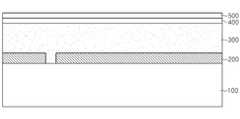
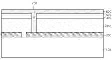
- a photovoltaic deviceincludes a support substrate 100, a back electrode layer 200, a light absorbing layer 300, a buffer layer 400, a high resistance buffer layer 500, and a front electrode layer. 600 and a plurality of connections 700.
- the support substrate 100has a plate shape, and the back electrode layer 200, the light absorbing layer 300, the buffer layer 400, the high resistance buffer layer 500, the front electrode layer 600, and the connection portion ( 700).
- the support substrate 100may be an insulator.
- the support substrate 100may be a glass substrate, a plastic substrate, or a metal substrate.
- the support substrate 100may be a soda lime glass substrate.
- the support substrate 100may be transparent.
- the support substrate 100may be rigid or flexible.
- the back electrode layer 200is disposed on the support substrate 100.
- the outer side surface 201 of the back electrode layer 200extends along the outer side of the support substrate 100. That is, the outer side surface 201 of the back electrode layer 200 corresponds to the outer side of the support substrate 100.
- the outer side surface 201 of the back electrode layer 200is disposed inside the outer side surface of the support substrate 100. That is, the outer side surface 201 of the back electrode layer 200 is disposed on a side different from the outer side surface of the support substrate 100. In addition, the back electrode layer 200 forms a step with the support substrate 100.
- the back electrode layer 200may have a rectangular shape in plan view.
- the back electrode layer 200is a conductive layer.
- Examples of the material used as the back electrode layer 200include a metal such as molybdenum.
- the back electrode layer 200may include two or more layers.
- each of the layersmay be formed of the same metal, or may be formed of different metals.
- First through holes P1are formed in the back electrode layer 200.
- the first through holes P1are open regions exposing the top surface of the support substrate 100.
- the first through holes P1may have a shape extending in one direction when viewed in a plan view.
- the width of the first through holes P1may be about 80 ⁇ m to 200 ⁇ m.
- the back electrode layer 200is divided into a plurality of back electrodes by the first through holes P1. That is, the back electrodes are defined by the first through holes P1.
- the back electrodesare spaced apart from each other by the first through holes P1.
- the back electrodesare arranged in a stripe shape.
- the back electrodesmay be arranged in a matrix form.
- the first through holes P1may have a lattice shape when viewed in a plan view.
- the light absorbing layer 300is disposed on the back electrode layer 200.
- the outer side surface 301 of the light absorbing layer 300corresponds to the outer side surface of the support substrate 100. That is, the outer side surface 301 of the light absorbing layer 300 extends along the outer side surface of the support substrate 100.
- the outer side surface 301 of the light absorbing layer 300is disposed inside the outer side surface of the support substrate 100. That is, the outer side surface 301 of the light absorbing layer 300 is disposed on a plane different from the outer side surface of the support substrate 100.
- the outer side surface 301 of the light absorbing layer 300is disposed on a plane different from the outer side surface 201 of the back electrode layer 200. In more detail, the outer side surface 301 of the light absorbing layer 300 is disposed outside the outer side surface 201 of the back electrode layer 200.
- the light absorbing layer 300forms a step with the back electrode layer 200. That is, the light absorbing layer 300 is stacked on the back electrode layer 200 and has an inverted step shape. That is, the distance between the outer side surface 301 of the light absorbing layer 300 and the outer side surface of the support substrate 100 is between the outer side surface 201 of the back electrode layer 200 and the outer side surface of the support substrate 100. Is smaller than the distance D2.
- a recess 210is formed between the light absorbing layer 300 and the support substrate 100.
- the outer side surface 301 of the light absorbing layer 300 and the outer side surface 201 of the back electrode layer 200may be spaced apart from each other by about 0.1 mm to about 10 mm.
- the light absorbing layer 300covers an area where the back electrode layer 200 is disposed. That is, the region where the light absorbing layer 300 is disposed is larger than the region where the back electrode layer 200 is disposed.
- the planar area of the light absorbing layer 300is larger than the planar area of the back electrode layer 200.
- the outer edge of the light absorbing layer 300surrounds the back electrode layer 200. That is, the outside of the back electrode layer 200 is disposed inside the outside of the light absorbing layer 300.
- the material included in the light absorbing layer 300is filled in the first through holes P1.
- the light absorbing layer 300may include a group I-III-VI compound.
- the light absorbing layer 300may be formed of a copper-indium-gallium-selenide-based (Cu (In, Ga) Se 2 ; CIGS-based) crystal structure, copper-indium-selenide-based, or copper-gallium-selenide It may have a system crystal structure.
- the energy band gap of the light absorbing layer 300may be about 1 eV to 1.8 eV.
- the buffer layer 400is disposed on the light absorbing layer 300.
- the buffer layer 400has the same planar shape as the light absorbing layer 300.
- the buffer layer 400includes cadmium sulfide (CdS), and an energy band gap of the buffer layer 400 is about 2.2 eV to 2.4 eV.
- the high resistance buffer layer 500is disposed on the buffer layer 400.
- the high resistance buffer layer 500has the same planar shape as the light absorbing layer 300.
- the high resistance buffer layer 500includes zinc oxide (iZnO) that is not doped with impurities.
- Second through holes P2are formed in the light absorbing layer 300, the buffer layer 400, and the high resistance buffer layer 500.
- the second through holes P2penetrate the light absorbing layer 300.
- the second through holes P2are open regions exposing the top surface of the back electrode layer 200.
- the second through holes P2are formed adjacent to the first through holes P1. That is, some of the second through holes P2 are formed next to the first through holes P1 when viewed in a plan view.
- the width of the second through holes P2may be about 80 ⁇ m to about 200 ⁇ m.
- the light absorbing layer 300defines a plurality of light absorbing portions by the second through holes P2. That is, the light absorbing layer 300 is divided into the light absorbing portions by the second through holes P2.
- the buffer layer 400is defined as a plurality of buffers by the second through holes P2. That is, the buffer layer 400 is divided into the buffers by the second through holes P2.
- the high resistance buffer layer 500defines a plurality of high resistance buffers by the second through holes P2. That is, the high resistance buffer layer 500 is divided into the high resistance buffers by the second through holes P2.
- the front electrode layer 600is disposed on the high resistance buffer layer 500.
- the front electrode layer 600may have a planar shape corresponding to the light absorbing layer 300.
- the outer side surface 601 of the front electrode layer 600may correspond to the outer side of the support substrate 100. That is, the outer side surface 601 of the front electrode layer 600 may extend along the outer side surface of the support substrate 100.
- the outer side surface 601 of the front electrode layer 600is disposed inward from the outer side surface of the support substrate 100. That is, the outer side surface 601 of the front electrode layer 600 is disposed on a plane different from the outer side surface of the support substrate 100.
- the outer side surface 601 of the front electrode layer 600may be disposed on the same plane as the outer side surface 301 of the light absorbing layer 300. That is, the front electrode layer 600 may coincide with the light absorbing layer 300 when viewed in a plan view.
- the outer side surface 601 of the front electrode layer 600may be disposed inside the outer side surface 301 of the light absorbing layer 300. That is, the front electrode layer 600 may be stacked with a step on the light absorbing layer 300.
- the outer side surface 601 of the front electrode layer 600may be disposed on a plane different from the outer side surface 201 of the rear electrode layer 200. In more detail, the outer side surface 601 of the front electrode layer 600 may be disposed outside the outer side surface 201 of the rear electrode layer 200.
- the distance W1 between the outer side surface 601 of the front electrode layer 600 and the outer side surface 201 of the back electrode layer 200may be about 0.1 mm to about 10 mm.
- the front electrode layer 600may cover an area where the rear electrode layer 200 is disposed. That is, an area where the front electrode layer 600 is disposed may be larger than an area where the rear electrode layer 200 is disposed.
- the planar area of the front electrode layer 600is larger than the area of the back electrode layer 200. Can be.
- the front electrode layer 600is transparent and is a conductive layer.
- the front electrode layer 600includes a conductive oxide.
- the front electrode layer 600may include zinc oxide, indium tin oxide (ITO), or indium zinc oxide (IZO).
- the oxidemay include a conductive dopant such as aluminum (Al), alumina (Al 2 O 3 ), magnesium (Mg), or gallium (Ga).
- a conductive dopantsuch as aluminum (Al), alumina (Al 2 O 3 ), magnesium (Mg), or gallium (Ga).
- the front electrode layer 600may include aluminum doped zinc oxide (AZO) or gallium doped zinc oxide (GZO).
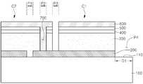
- Third through holes P3are formed in the light absorbing layer 300, the buffer layer 400, the high resistance buffer layer 500, and the front electrode layer 600.
- the third through holes P3are open regions exposing the top surface of the back electrode layer 200.
- the width of the third through holes P3may be about 80 ⁇ m to about 200 ⁇ m.
- the third through holes P3are formed at positions adjacent to the second through holes P2.
- the third through holes P3are disposed next to the second through holes P2. That is, when viewed in plan, the third through holes P3 are arranged side by side next to the second through holes P2.
- the front electrode layer 600is divided into a plurality of front electrodes by the third through holes P3. That is, the front electrodes are defined by the third through holes P3.
- the front electrodeshave a shape corresponding to the rear electrodes. That is, the front electrodes are arranged in a stripe shape. Alternatively, the front electrodes may be arranged in a matrix form.
- a plurality of cells C1, C2...are defined by the third through holes P3.
- the cellsare defined by the second through holes P2 and the third through holes P3. That is, the photovoltaic device according to the embodiment is divided into the cells C1, C2... By the second through holes P2 and the third through holes P3.
- connection parts 700are disposed inside the second through holes P2.
- the connection parts 700extend downward from the front electrode layer 600 and are connected to the back electrode layer 200.
- connection parts 700connect adjacent cells to each other.
- the connection parts 700connect the front electrode and the back electrode included in the cells adjacent to each other.
- connection part 700is formed integrally with the front electrode layer 600. That is, the material used as the connection part 700 is the same as the material used as the front electrode layer 600.
- the outer side surface 201 of the back electrode layer 200 and the outer side surface 601 of the front electrode layer 600are disposed on different planes. Accordingly, the distance between the outer side surface 201 of the rear electrode layer 200 and the outer side surface 601 of the front electrode layer 600 is increased.
- the back electrode layer 200forms a step with the light absorbing layer 300. Accordingly, as the distance between the outer side surface 201 of the back electrode layer 200 and the outer side surface 301 of the light absorbing layer 300 increases, the outer side surface 201 of the back electrode layer 200 and the The distance between the outer side surfaces 601 of the front electrode layer 600 is increased.
- the solar cell apparatusmay prevent a short between the outer side surface 201 of the rear electrode layer 200 and the outer side surface 601 of the front electrode layer 600.
- the solar cell apparatus according to the embodimentmay block the leakage current generated through the outer side surface 201 of the back electrode layer 200 and the outer side surface 601 of the front electrode layer 600.
- the photovoltaic device according to the embodimentmay prevent short circuits and leakage currents in the back electrode layer 200 and the front electrode layer 600. Therefore, the solar cell apparatus according to the embodiment has improved electrical characteristics and may have high photoelectric conversion efficiency.
- 3 to 11are diagrams illustrating a method of manufacturing the solar cell apparatus according to the embodiment.
- the description of the solar cell apparatus according to the embodimentmay be combined with the description of the solar cell apparatus described above.
- the back electrode layer 200is formed on the support substrate 100.
- the support substrate 100may be glass, and a ceramic substrate, a metal substrate, or a polymer substrate may also be used.
- soda lime glass or high strained point soda glassmay be used as the glass substrate.
- a substrate including stainless steel or titaniummay be used.
- polymer substratepolyimide may be used.
- the support substrate 100may be transparent.
- the substrate 100may be rigid or flexible.
- the back electrode layer 200may be formed of a conductor such as metal.
- the back electrode layer 200may be formed by a sputtering process using molybdenum (Mo) as a target.
- Momolybdenum
- the molybdenum (Mo) thin filmwhich is the back electrode layer 200, must have a low specific resistance as an electrode and have excellent adhesion to the substrate 100 so that peeling does not occur due to a difference in thermal expansion coefficient.
- the material forming the back electrode layer 200is not limited thereto, and may be formed of molybdenum (Mo) doped with sodium (Na) ions.
- the back electrode layer 200may be formed of at least one layer.
- the layers constituting the back electrode layer 200may be formed of different materials.
- first through holes P1may be formed in the back electrode layer 200, and the back electrode layers 200 may be separated from each other.
- the first through holes P1may selectively expose the top surface of the substrate 100.
- the first through holes P1may be patterned by a mechanical device or a laser device.
- the width of the first through holes P1may be about 60 ⁇ m to about 100 ⁇ m.
- the back electrode layer 200may be arranged in a stripe form or a matrix form by the first through holes P1 and may correspond to each cell.
- the back electrode layer 200is not limited to the above form, it may be formed in various forms.
- a light absorbing layer 300is formed on the back electrode layer 200 and the first through holes P1.
- the light absorbing layer 300includes an I-III-VI group compound.
- the light absorbing layer 300may include a copper-indium-gallium-selenide-based (Cu (In, Ga) Se 2 , CIGS-based) compound.
- the light absorbing layer 300may include a copper-indium selenide-based (CuInSe 2 , CIS-based) compound or a copper-gallium-selenide-based (CuGaSe 2 , CGS-based) compound.
- CuInSe 2copper-indium selenide-based
- CIS-basedcopper-indium selenide-based
- CuGaSe 2copper-gallium-selenide-based
- CGS-basedcopper-gallium-selenide-based
- a CIG-based metal precursor filmis formed on the back electrode layer 200 using a copper target, an indium target, and a gallium target.
- the metal precursor filmis reacted with selenium (Se) by a selenization process to form a CIGS light absorbing layer.
- Seselenium
- the light absorbing layer 300may form copper, indium, gallium, selenide (Cu, In, Ga, Se) by co-evaporation.
- the light absorbing layer 300receives external light and converts the light into electrical energy.
- the light absorbing layer 300generates photo electromotive force by the photoelectric effect.
- a buffer layer 400 and a high resistance buffer layer 500are formed on the light absorbing layer 300.
- the buffer layer 400may be formed of at least one layer on the light absorbing layer 300.
- the buffer layer 400may be formed by stacking cadmium sulfide (CdS) by a CBD process.
- the buffer layer 400is an n-type semiconductor layer, and the light absorbing layer 300 is a p-type semiconductor layer. Thus, the light absorbing layer 300 and the buffer layer 400 form a pn junction.
- the high resistance buffer layer 500may be formed as a transparent electrode layer on the buffer layer 400.
- the high resistance buffer layer 500may be formed of any one of ITO, ZnO, and i-ZnO.
- the high resistance buffer layer 500may be formed of a zinc oxide layer by performing a sputtering process targeting zinc oxide (ZnO).
- the buffer layer 400 and the high resistance buffer layer 500are disposed between the light absorbing layer 300 and a front electrode formed thereafter.
- the buffer layer 400 and the high resistance buffer layer 500 having a band gap in between the two materialsare inserted.
- a junctioncan be formed.
- two buffer layers 400are formed on the light absorbing layer 300, but the present invention is not limited thereto.
- the buffer layer 400may be formed of only one layer.
- the second through holes P2may be formed by a mechanical device such as a tip or a laser device.
- the second through holes P2may be formed adjacent to the first through holes P1.
- the width of the second through holes P2may be about 60 ⁇ m to about 100 ⁇ m, and the gap between the second through holes P2 and the first through holes P1 may be about. 60 ⁇ m to about 100 ⁇ m.
- the front electrode layer 600is formed by stacking a transparent conductive material on the high resistance buffer layer 500.
- the transparent conductive materialmay be deposited on the second through holes P2 to form a connection wiring 700.
- the front electrode layer 600is formed of zinc oxide doped with aluminum (Al) or alumina (Al 2 O 3 ) by a sputtering process.
- the front electrode layer 600is a window layer forming a pn junction with the light absorbing layer 300. Since the front electrode layer functions as a transparent electrode on the front of the solar cell, zinc oxide (ZnO) having high light transmittance and good electrical conductivity is provided. Is formed.
- ZnOzinc oxide
- the zinc oxide thin filmwhich is the front electrode layer 600, may be formed by a method of depositing using a ZnO target by RF sputtering, reactive sputtering using a Zn target, and organometallic chemical vapor deposition.
- ITOindium thin oxide
- third through holes P3 penetrating the front electrode layer 600, the high resistance buffer layer 500, the buffer layer 400, and the light absorbing layer 300are formed.
- the third through holes P3may selectively expose the back electrode layer 200.
- the third through holes P3may be formed to be adjacent to the second through holes P2.
- the width of the third through holes P3may be about 60 ⁇ m to about 100 ⁇ m, and the gap between the third through holes P3 and the second through holes P2 may be about. 60 ⁇ m to about 100 ⁇ m.
- the third through holes P3may be irradiated with a laser or may be formed by a mechanical method such as a tip.
- the light absorption layer 300, the buffer layer 400, the high resistance buffer layer 500, and the front electrode layer 600may be separated by unit cells by the third through holes P3. That is, the cells C1, C2... May be separated from each other by the third through holes P3.
- the light absorbing layer 300, the buffer layer 400, the high resistance buffer layer 500, and the front electrode layer 600may be arranged in a stripe shape or a matrix shape by the third through holes P3.
- the third through holes P3are not limited to the above shapes, but may be formed in various shapes.
- each of the cells C1 and C2may be connected to each other by the connection wiring 700. That is, the connection wiring 700 may physically and electrically connect the rear electrode of the second cell C2 and the front electrode of the first cell C1 adjacent to the second cell C2.
- a first edge pattern P4is formed around the rear electrode layer 200, the light absorbing layer 300, the buffer layer 400, the high resistance buffer layer 500, and the front electrode layer 600. .
- the first edge pattern P4may be formed by a mechanical scribing process such as a tip or a laser.
- a lasermay be used to remove the outer portion of the back electrode layer 200.
- Side surfaces of the back electrode layer 200, the light absorbing layer 300, the buffer layer 400, the high resistance buffer layer 500, and the front electrode layer 600 formed by the first removal processmay be formed on the support substrate 100. It may be perpendicular to the upper surface of the).
- side surfaces of the back electrode layer 200, the light absorbing layer 300, the buffer layer 400, the high resistance buffer layer 500, and the front electrode layer 600 formed by the first removal processare the same plane. May be disposed on and have a uniform surface.
- the non-uniform portionscan be removed collectively, the performance of the solar cell apparatus according to the embodiment can be improved as a whole.
- the outer portion of the back electrode layer 200is secondarily removed. Accordingly, the second edge pattern 210 is formed outside the back electrode layer 200.
- the second edge pattern 210is a recess 210 formed between the light absorbing layer 300 and the support substrate 100.
- the secondary removal processmay be an etching process.
- the outer portion of the back electrode layer 200is secondarily removed by a wet etching process.
- an etchant capable of selectively etching the back electrode layer 200may be used.
- the etchantmay include an etchant or hydrogen peroxide etchant comprising phosphoric acid, nitric acid and acetic acid.
- the secondary removal processmay be performed by spraying the etchant to the outer portion of the back electrode layer 200.
- an outer portion of the back electrode layer 200may be removed by an etching apparatus including a nozzle for injecting the etchant and a backing for sucking the injected etchant and by-products.
- the nozzlesprays the etchant to the outer portion of the back electrode layer 200 while moving along the outer portion of the back electrode layer 200.
- the backingsucks in the etchant injected by the nozzle and by-products of the etching process.
- the backingcan be moved with the nozzle.
- the width D2 of the second edge pattern 210is larger than the width D1 of the first edge pattern P4. That is, the outer side surface 201 of the back electrode layer 200 has a shape recessed inward with respect to the outer side surface 301 of the light absorbing layer 300.
- the secondary removal processincludes an etching process
- by-products generated in the primary removal processmay be efficiently removed. That is, by-products such as particles generated by a mechanical scribing or laser process are removed. Therefore, the solar cell apparatus according to the embodiment can prevent the short caused by the by-products.
- the manufacturing method of the solar cell apparatuscan prevent the electrical connection between the front electrode layer 600 and the rear electrode layer 200.
- the manufacturing method of the solar cell apparatuscan prevent the electrical connection between the front electrode layer 600 and the rear electrode layer 200.
- the manufacturing method of the solar cell apparatuscan prevent the electrical connection between the front electrode layer 600 and the rear electrode layer 200.
- the manufacturing method of the solar cell apparatuscan prevent the electrical connection between the front electrode layer 600 and the rear electrode layer 200.
- the manufacturing method of the solar cell apparatuscan prevent the electrical connection between the front electrode layer 600 and the rear electrode layer 200.
- the electrical short circuit in the outer portion of the photovoltaic deviceis prevented. And insulation can be ensured.
- FIG. 12 and 13are views illustrating another manufacturing method of the solar cell apparatus according to the embodiment.
- the description of the foregoing photovoltaic device and a description of the manufacturing method thereofmay be essentially combined.
- the back electrode layer 200, the light absorbing layer 300, the buffer layer 400, the high resistance buffer layer 500, and the front electrode layer 600are sequentially formed on the support substrate 100.
- the primary removal processcan be carried out by a mechanical method such as a tip.
- the light absorbing layer 300, the buffer layer 400, the high resistance buffer layer 500, and the front electrode layer 600may have a crystal structure, they may be effectively removed by a mechanical method.
- the back electrode layer 200may be formed of metal, the back electrode layer 200 may remain without being removed in the first removal process.
- the outer portion of the back electrode layer 200is secondarily removed by the etching process described in the foregoing manufacturing method.
- the conditions of the secondary removal processis adjusted, so that the outer side surface 201 of the back electrode layer 200 subjected to the secondary process has a structure recessed with respect to the outer side surface 301 of the light absorbing layer 300.
- the first edge pattern P4 and the second edge pattern 210are formed without using a laser.
- the present manufacturing methodcan provide a photovoltaic device having no photoresist and preventing shorting and having improved photoelectric conversion efficiency.
- Photovoltaic deviceis used in the field of photovoltaic power generation.
Landscapes
- Photovoltaic Devices (AREA)
Abstract
Description
Translated fromKorean실시예는 태양광 발전장치 및 이의 제조방법에 관한 것이다.The embodiment relates to a photovoltaic device and a method of manufacturing the same.
최근 에너지 수요가 증가함에 따라서, 태양광 에너지를 전기에너지로 변환시키는 태양전지에 대한 개발이 진행되고 있다.Recently, as energy demand increases, development of a solar cell converting solar energy into electrical energy is in progress.
특히, 유리 기판, 금속 후면 전극층, p형 CIGS 계 광 흡수층, 고저항 버퍼층, n형 창층 등을 포함하는 기판 구조의 pn 헤테로 접합 장치인 CIGS계 태양전지가 널리 사용되고 있다.In particular, CIGS-based solar cells that are pn heterojunction devices having a substrate structure including a glass substrate, a metal back electrode layer, a p-type CIGS-based light absorbing layer, a high resistance buffer layer, an n-type window layer, and the like are widely used.
이러한 태양전지는 기판 후면부터 차례로 증착 형성되는 것으로, 각층들이 부분적으로 증착 수준이 다른 영역이 존재할 수 있다.Such a solar cell is formed by sequentially depositing from the back of the substrate, and there may exist regions where the layers have partial deposition levels.
이에 따라, 태양전지 모듈이 외부와 연결되어 단락되는 문제가 발생될 수 있으며, 이는 태양전지의 전기적 특성을 저하시킬 수 있다.Accordingly, a problem may occur in which the solar cell module is connected to the outside and short-circuited, which may lower the electrical characteristics of the solar cell.
실시예는 기판의 에지 영역에서 누설전류(leakage current)를 차단하여, 향상된 전기적인 특성을 가지는 태양광 발전장치 및 이의 제조방법을 제공하고자 한다.Embodiments provide a photovoltaic device having improved electrical characteristics and a method of manufacturing the same by blocking leakage current in an edge region of a substrate.
일 실시예에 따른 태양광 발전장치는 기판; 상기 기판 상에 배치되는 후면전극층; 상기 후면전극층 상에 배치되는 광 흡수층; 및 상기 광 흡수층 상에 배치되는 전면전극층을 포함하고, 상기 후면전극층의 외곽 측면은 상기 광 흡수층의 외곽 측면과 서로 다른 평면에 배치된다.Photovoltaic device according to one embodiment includes a substrate; A rear electrode layer disposed on the substrate; A light absorbing layer disposed on the back electrode layer; And a front electrode layer disposed on the light absorbing layer, and the outer side surface of the back electrode layer is disposed on a different plane from the outer side surface of the light absorbing layer.
실시예에 따른 태양광 발전장치의 제조방법은 기판 상에 후면전극층을 형성하는 단계; 상기 후면전극층 상에 광 흡수층을 형성하는 단계; 상기 광 흡수층 상에 전면전극층을 형성하는 단계; 상기 후면전극층, 상기 광 흡수층 및 상기 전면전극층의 외곽 부분을 1차 제거하는 단계; 및 상기 1차 제거된 후면전극층의 외곽 부분을 2차 제거하는 단계를 포함한다.Method of manufacturing a solar cell apparatus according to the embodiment comprises the steps of forming a back electrode layer on a substrate; Forming a light absorbing layer on the back electrode layer; Forming a front electrode layer on the light absorbing layer; Firstly removing outer portions of the rear electrode layer, the light absorbing layer, and the front electrode layer; And secondly removing the outer portion of the first removed back electrode layer.
실시예에 따른 태양광 발전장치의 제조방법은 기판 상에 후면전극층을 형성하는 단계; 상기 후면전극층 상에 광 흡수층을 형성하는 단계; 상기 광 흡수층 상에 전면전극층을 형성하는 단계; 상기 광 흡수층 및 상기 전면전극층의 외곽 부분을 1차 제거하는 단계; 및 상기 후면전극층의 외곽 부분을 2차 제거하는 단계를 포함한다.Method of manufacturing a solar cell apparatus according to the embodiment comprises the steps of forming a back electrode layer on a substrate; Forming a light absorbing layer on the back electrode layer; Forming a front electrode layer on the light absorbing layer; Firstly removing outer portions of the light absorbing layer and the front electrode layer; And secondly removing an outer portion of the back electrode layer.
실시예에 따른 태양광 발전장치는 후면전극층의 외곽 측면 및 광 흡수층의 외곽 측면을 다른 평면에 배치시킨다. 상기 후면전극층의 외곽 측면은 안쪽으로 함몰된 구조를 가질 수 있다. 이에 따라서, 후면전극층의 외곽 측면 및 전면전극층의 외곽 측면 사이의 거리는 함몰된만큼 증가될 수 있다.In the solar cell apparatus according to the embodiment, the outer side of the rear electrode layer and the outer side of the light absorbing layer are disposed on different planes. The outer side surface of the back electrode layer may have a structure recessed inward. Accordingly, the distance between the outer side surface of the rear electrode layer and the outer side surface of the front electrode layer can be increased by being depressed.
따라서, 실시예에 따른 태양광 발전장치는 후면전극층의 외곽 측면 및 전면전극층의 외곽 측면 사이의 쇼트를 방지할 수 있다. 또한, 실시예에 따른 태양광 발전장치는 후면전극층의 외곽 측면 및 전면전극층의 외곽 측면을 통하여 발생되는 누설 전류를 차단할 수 있다.Thus, the solar cell apparatus according to the embodiment can prevent a short between the outer side of the rear electrode layer and the outer side of the front electrode layer. In addition, the solar cell apparatus according to the embodiment may block the leakage current generated through the outer side of the rear electrode layer and the outer side of the front electrode layer.
또한, 실시예에 따른 태양광 발전장치의 제조방법은 외곽 영역을 레이저를 사용하지 않고 패터닝할 수 있다. 즉, 기계적인 스크라이빙 및 식각 공정만으로 에지 제거 공정(edge deletion)이 진행될 수 있다.In addition, the manufacturing method of the solar cell apparatus according to the embodiment can pattern the outer region without using a laser. That is, the edge deletion process may be performed only by the mechanical scribing and etching process.
따라서, 실시예에 따른 태양광 발전장치는 용이하게 형성될 수 있다.Therefore, the solar cell apparatus according to the embodiment can be easily formed.
또한, 실시예에 따른 태양광 발전장치의 제조방법은 외곽 영역을 1차 패터닝하고, 추가적으로 식각액을 사용하여 2차 패터닝할 수 있다. 이에 따라서, 외곽 부분의 불순물이 제거되고, 불순물에 의한 쇼트 등이 방지될 수 있다.In addition, in the method of manufacturing the solar cell apparatus according to the embodiment, the outer region may be first patterned, and additionally, the second patterning may be performed using an etchant. Accordingly, impurities in the outer portion can be removed, and shorts due to impurities can be prevented.
따라서, 실시예에 따른 태양광 발전장치는 후면전극층 및 전면전극층에서의 쇼트 및 누설 전류 등을 방지할 수 있다. 따라서, 실시예에 따른 태양광 발전장치는 향상된 전기적인 특성을 가지고, 높은 광-전 변환 효율을 가질 수 있다.Therefore, the solar cell apparatus according to the embodiment can prevent the short and the leakage current in the rear electrode layer and the front electrode layer. Therefore, the solar cell apparatus according to the embodiment has improved electrical characteristics and may have high photoelectric conversion efficiency.
도 1은 실시예에 따른 태양광 발전장치를 도시한 평면도이다.1 is a plan view illustrating a solar cell apparatus according to an embodiment.
도 2는 1에서 A-A`를 따라서 절단한 단면을 도시한 단면도이다.FIG. 2 is a cross-sectional view taken along a line A-A 'in FIG.
도 3 내지 도 11은 실시예에 따른 태양광 발전장치의 일 제조방법을 도시한 도면들이다.3 to 11 are diagrams illustrating a method of manufacturing the solar cell apparatus according to the embodiment.
도 12 및 도 13은 실시예에 따른 태양광 발전장치의 다른 제조방법을 도시한 도면들이다.12 and 13 are views illustrating another manufacturing method of the solar cell apparatus according to the embodiment.
실시 예의 설명에 있어서, 각 기판, 층, 막 또는 전극 등이 각 기판, 층, 막, 또는 전극 등의 "상(on)"에 또는 "아래(under)"에 형성되는 것으로 기재되는 경우에 있어, "상(on)"과 "아래(under)"는 "직접(directly)" 또는 "다른 구성요소를 개재하여 (indirectly)" 형성되는 것을 모두 포함한다. 또한 각 구성요소의 상 또는 아래에 대한 기준은 도면을 기준으로 설명한다. 도면에서의 각 구성요소들의 크기는 설명을 위하여 과장될 수 있으며, 실제로 적용되는 크기를 의미하는 것은 아니다.In the description of the embodiments, where each substrate, layer, film, or electrode is described as being formed "on" or "under" of each substrate, layer, film, or electrode, etc. , "On" and "under" include both "directly" or "indirectly" formed through other components. In addition, the criteria for the top or bottom of each component will be described with reference to the drawings. The size of each component in the drawings may be exaggerated for description, and does not mean a size that is actually applied.
도 1은 실시예에 따른 태양광 발전장치를 도시한 평면도이다. 도 2는 1에서 A-A`를 따라서 절단한 단면을 도시한 단면도이다.1 is a plan view illustrating a solar cell apparatus according to an embodiment. FIG. 2 is a cross-sectional view taken along a line A-A 'in FIG.
도 1 및 도 2를 참조하면, 실시예에 따른 태양광 발전장치는 지지기판(100), 후면전극층(200), 광 흡수층(300), 버퍼층(400), 고저항 버퍼층(500), 전면전극층(600) 및 다수 개의 접속부들(700)을 포함한다.1 and 2, a photovoltaic device according to an embodiment includes a
상기 지지기판(100)은 플레이트 형상을 가지며, 상기 후면전극층(200), 상기 광 흡수층(300), 상기 버퍼층(400), 상기 고저항 버퍼층(500), 상기 전면전극층(600) 및 상기 접속부(700)를 지지한다.The
상기 지지기판(100)은 절연체일 수 있다. 상기 지지기판(100)은 유리기판, 플라스틱기판 또는 금속기판일 수 있다. 더 자세하게, 상기 지지기판(100)은 소다 라임 글래스(soda lime glass) 기판일 수 있다. 상기 지지기판(100)은 투명할 수 있다. 상기 지지기판(100)은 리지드하거나 플렉서블할 수 있다.The
상기 후면전극층(200)은 상기 지지기판(100) 상에 배치된다. 상기 후면전극층(200)의 외곽 측면(201)은 상기 지지기판(100)의 외곽을 따라서 연장된다. 즉, 상기 후면전극층(200)의 외곽 측면(201)은 상기 지지기판(100)의 외곽에 대응된다.The
상기 후면전극층(200)의 외곽 측면(201)은 상기 지지기판(100)의 외곽 측면의 내측에 배치된다. 즉, 상기 후면전극층(200)의 외곽 측면(201)은 상기 지지기판(100)의 외곽 측면과 다른 측면에 배치된다. 또한, 상기 후면전극층(200)은 상기 지지기판(100)과 단차를 형성한다.The
상기 후면전극층(200)은 평면에서 보았을 때 직사각형 형상을 가질 수 있다. 상기 후면전극층(200)은 도전층이다. 상기 후면전극층(200)으로 사용되는 물질의 예로서는 몰리브덴 등의 금속을 들 수 있다.The
또한, 상기 후면전극층(200)은 두 개 이상의 층들을 포함할 수 있다. 이때, 각각의 층들은 같은 금속으로 형성되거나, 서로 다른 금속으로 형성될 수 있다.In addition, the
상기 후면전극층(200)에는 제 1 관통홈들(P1)이 형성된다. 상기 제 1 관통홈들(P1)은 상기 지지기판(100)의 상면을 노출하는 오픈 영역이다. 상기 제 1 관통홈들(P1)은 평면에서 보았을 때, 일 방향으로 연장되는 형상을 가질 수 있다.First through holes P1 are formed in the
상기 제 1 관통홈들(P1)의 폭은 약 80㎛ 내지 200㎛ 일 수 있다.The width of the first through holes P1 may be about 80 μm to 200 μm.
상기 제 1 관통홈들(P1)에 의해서, 상기 후면전극층(200)은 다수 개의 후면전극들로 구분된다. 즉, 상기 제 1 관통홈들(P1)에 의해서, 상기 후면전극들이 정의된다.The
상기 후면전극들은 상기 제 1 관통홈들(P1)에 의해서 서로 이격된다. 상기 후면전극들은 스트라이프 형태로 배치된다.The back electrodes are spaced apart from each other by the first through holes P1. The back electrodes are arranged in a stripe shape.
이와는 다르게, 상기 후면전극들은 매트릭스 형태로 배치될 수 있다. 이때, 상기 제 1 관통홈들(P1)은 평면에서 보았을 때, 격자 형태로 형성될 수 있다.Alternatively, the back electrodes may be arranged in a matrix form. In this case, the first through holes P1 may have a lattice shape when viewed in a plan view.
상기 광 흡수층(300)은 상기 후면전극층(200) 상에 배치된다. 상기 광 흡수층(300)의 외곽 측면(301)은 상기 지지기판(100)의 외곽 측면에 대응된다. 즉, 상기 광 흡수층(300)의 외곽 측면(301)은 상기 지지기판(100)의 외곽 측면을 따라서 연장된다.The light absorbing
상기 광 흡수층(300)의 외곽 측면(301)은 상기 지지기판(100)의 외곽 측면의 안쪽에 배치된다. 즉, 상기 광 흡수층(300)의 외곽 측면(301)은 상기 지지기판(100)의 외곽 측면과 다른 평면에 배치된다.The
또한, 상기 광 흡수층(300)의 외곽 측면(301)은 상기 후면전극층(200)의 외곽 측면(201)과 다른 평면에 배치된다. 더 자세하게, 상기 광 흡수층(300)의 외곽 측면(301)은 상기 후면전극층(200)의 외곽 측면(201)보다 더 바깥쪽에 배치된다.In addition, the
이에 따라서, 상기 광 흡수층(300)은 상기 후면전극층(200)과 단차를 형성한다. 즉, 상기 광 흡수층(300)은 상기 후면전극층(200) 상에 뒤집어진 계단 형상을 가지며 적층된다. 즉, 상기 광 흡수층(300)의 외곽 측면(301) 및 상기 지지기판(100)의 외곽 측면 사이의 거리는 상기 후면전극층(200)의 외곽 측면(201) 및 상기 지지기판(100)의 외곽 측면 사이의 거리(D2)보다 더 작다.Accordingly, the
이에 따라서, 상기 광 흡수층(300) 및 상기 지지기판(100) 사이에 리세스(210)가 형성된다. 또한, 상기 광 흡수층(300)의 외곽 측면(301) 및 상기 후면전극층(200)의 외곽 측면(201)은 약 0.1㎜ 내지 약 10㎜ 만큼 서로 이격될 수 있다.Accordingly, a
상기 광 흡수층(300)은 상기 후면전극층(200)이 배치되는 영역을 덮는다. 즉, 상기 광 흡수층(300)이 배치되는 영역은 상기 후면전극층(200)이 배치되는 영역보다 더 크다. 상기 광 흡수층(300)의 평면적은 상기 후면전극층(200)의 평면적보다 더 크다.The light
상기 광 흡수층(300)의 외곽은 상기 후면전극층(200)을 둘러싼다. 즉, 상기 후면전극층(200)의 외곽은 상기 광 흡수층(300)의 외곽 내측에 배치된다. 상기 광 흡수층(300)에 포함된 물질은 상기 제 1 관통홈들(P1)에 채워진다.The outer edge of the
상기 광 흡수층(300)은 Ⅰ-Ⅲ-Ⅵ족 계 화합물을 포함할 수 있다. 예를 들어, 상기 광 흡수층(300)은 구리-인듐-갈륨-셀레나이드계(Cu(In,Ga)Se2;CIGS계) 결정 구조, 구리-인듐-셀레나이드계 또는 구리-갈륨-셀레나이드계 결정 구조를 가질 수 있다.The light
상기 광 흡수층(300)의 에너지 밴드갭(band gap)은 약 1eV 내지 1.8eV일 수 있다.The energy band gap of the
상기 버퍼층(400)은 상기 광 흡수층(300) 상에 배치된다. 상기 버퍼층(400)은 상기 광 흡수층(300)과 동일한 평면 형상을 가진다. 상기 버퍼층(400)은 황화 카드뮴(CdS)를 포함하며, 상기 버퍼층(400)의 에너지 밴드갭은 약 2.2eV 내지 2.4eV이다.The
상기 고저항 버퍼층(500)은 상기 버퍼층(400) 상에 배치된다. 상기 고저항 버퍼층(500)은 상기 광 흡수층(300)과 동일한 평면 형상을 가진다. 상기 고저항 버퍼층(500)은 불순물이 도핑되지 않은 징크 옥사이드(iZnO)를 포함한다.The high
상기 광 흡수층(300), 상기 버퍼층(400) 및 상기 고저항 버퍼층(500)에는 제 2 관통홈들(P2)이 형성된다. 상기 제 2 관통홈들(P2)은 상기 광 흡수층(300)을 관통한다. 또한, 상기 제 2 관통홈들(P2)은 상기 후면전극층(200)의 상면을 노출하는 오픈영역이다.Second through holes P2 are formed in the
상기 제 2 관통홈들(P2)은 상기 제 1 관통홈들(P1)에 인접하여 형성된다. 즉, 상기 제 2 관통홈들(P2)의 일부는 평면에서 보았을 때, 상기 제 1 관통홈들(P1)의 옆에 형성된다.The second through holes P2 are formed adjacent to the first through holes P1. That is, some of the second through holes P2 are formed next to the first through holes P1 when viewed in a plan view.
상기 제 2 관통홈들(P2)의 폭은 약 80㎛ 내지 약 200㎛ 일 수 있다.The width of the second through holes P2 may be about 80 μm to about 200 μm.
또한, 상기 광 흡수층(300)은 상기 제 2 관통홈들(P2)에 의해서, 다수 개의 광 흡수부들을 정의한다. 즉, 상기 광 흡수층(300)은 상기 제 2 관통홈들(P2)에 의해서, 상기 광 흡수부들로 구분된다.In addition, the
상기 버퍼층(400)은 상기 제 2 관통홈들(P2)에 의해서, 다수 개의 버퍼들로 정의된다. 즉, 상기 버퍼층(400)은 상기 제 2 관통홈들(P2)에 의해서, 상기 버퍼들로 구분된다.The
상기 고저항 버퍼층(500)은 상기 제 2 관통홈들(P2)에 의해서, 다수 개의 고저항 버퍼들을 정의한다. 즉, 상기 고저항 버퍼층(500)은 상기 제 2 관통홈들(P2)에 의해서, 상기 고저항 버퍼들로 구분된다.The high
상기 전면전극층(600)은 상기 고저항 버퍼층(500) 상에 배치된다. 상기 전면전극층(600)은 상기 광 흡수층(300)에 대응되는 평면 형상을 가질 수 있다.The
상기 전면전극층(600)의 외곽 측면(601)은 상기 지지기판(100)의 외곽에 대응될 수 있다. 즉, 상기 전면전극층(600)의 외곽 측면(601)은 상기 지지기판(100)의 외곽 측면을 따라서 연장될 수 있다.The
상기 전면전극층(600)의 외곽 측면(601)은 상기 지지기판(100)의 외곽 측면보다 안쪽에 배치된다. 즉, 상기 전면전극층(600)의 외곽 측면(601)은 상기 지지기판(100)의 외곽 측면과 다른 평면에 배치된다.The
상기 전면전극층(600)의 외곽 측면(601)은 상기 광 흡수층(300)의 외곽 측면(301)과 동일한 평면에 배치될 수 있다. 즉, 상기 전면전극층(600)은 평면에서 보았을 때, 상기 광 흡수층(300)과 일치될 수 있다.The
이와는 다르게, 상기 전면전극층(600)의 외곽 측면(601)은 상기 광 흡수층(300)의 외곽 측면(301)보다 안쪽에 배치될 수 있다. 즉, 상기 전면전극층(600)은 상기 광 흡수층(300) 상에 단차를 가지며 적층될 수 있다.Alternatively, the
상기 전면전극층(600)의 외곽 측면(601)은 상기 후면전극층(200)의 외곽 측면(201)과 다른 평면에 배치될 수 있다. 더 자세하게, 상기 전면전극층(600)의 외곽 측면(601)은 상기 후면전극층(200)의 외곽 측면(201)보다 더 바깥쪽에 배치될 수 있다.The
이에 따라서, 상기 전면전극층(600)의 외곽 측면(601) 및 상기 후면전극층(200)의 외곽 측면(201) 사이의 거리(W1)는 약 0.1㎜ 내지 약 10㎜ 일 수 있다.Accordingly, the distance W1 between the
상기 전면전극층(600)은 상기 후면전극층(200)이 배치되는 영역을 덮을 수 있다. 즉, 상기 전면전극층(600)이 배치되는 영역은 상기 후면전극층(200)이 배치되는 영역보다 더 클 수 있다.. 상기 전면전극층(600)의 평면적은 상기 후면전극층(200)의 평면적보다 더 클 수 있다.The
상기 전면전극층(600)은 투명하며, 도전층이다. 상기 전면전극층(600)은 도전성 산화물을 포함한다. 예를 들어, 상기 전면전극층(600)은 징크 옥사이드(zinc oxide), 인듐 틴 옥사이드(induim tin oxide;ITO) 또는 인듐 징크 옥사이드(induim zinc oxide;IZO) 등을 포함할 수 있다.The
또한, 상기 산화물은 알루미늄(Al), 알루미나(Al2O3), 마그네슘(Mg) 또는 갈륨(Ga) 등의 도전성 도펀트를 포함할 수 있다. 더 자세하게, 상기 전면전극층(600)은 알루미늄 도핑된 징크 옥사이드(Al doped zinc oxide;AZO) 또는 갈륨 도핑된 징크 옥사이드(Ga doped zinc oxide;GZO) 등을 포함할 수 있다.In addition, the oxide may include a conductive dopant such as aluminum (Al), alumina (Al2 O3 ), magnesium (Mg), or gallium (Ga). In more detail, the
상기 광 흡수층(300), 상기 버퍼층(400), 상기 고저항 버퍼층(500) 및 상기 전면전극층(600)에는 제 3 관통홈들(P3)이 형성된다. 상기 제 3 관통홈들(P3)은 상기 후면전극층(200)의 상면을 노출하는 오픈 영역이다. 예를 들어, 상기 제 3 관통홈들(P3)의 폭은 약 80㎛ 내지 약 200㎛일 수 있다.Third through holes P3 are formed in the
상기 제 3 관통홈들(P3)은 상기 제 2 관통홈들(P2)에 인접하는 위치에 형성된다. 더 자세하게, 상기 제 3 관통홈들(P3)은 상기 제 2 관통홈들(P2) 옆에 배치된다. 즉, 평면에서 보았을 때, 상기 제 3 관통홈들(P3)은 상기 제 2 관통홈들(P2) 옆에 나란히 배치된다.The third through holes P3 are formed at positions adjacent to the second through holes P2. In more detail, the third through holes P3 are disposed next to the second through holes P2. That is, when viewed in plan, the third through holes P3 are arranged side by side next to the second through holes P2.
상기 제 3 관통홈들(P3)에 의해서, 상기 전면전극층(600)은 다수 개의 전면전극들로 구분된다. 즉, 상기 전면전극들은 상기 제 3 관통홈들(P3)에 의해서 정의된다.The
상기 전면전극들은 상기 후면전극들과 대응되는 형상을 가진다. 즉, 상기 전면전극들은 스트라이프 형태로 배치된다. 이와는 다르게, 상기 전면전극들은 매트릭스 형태로 배치될 수 있다.The front electrodes have a shape corresponding to the rear electrodes. That is, the front electrodes are arranged in a stripe shape. Alternatively, the front electrodes may be arranged in a matrix form.
또한, 상기 제 3 관통홈들(P3)에 의해서, 다수 개의 셀들(C1, C2...)이 정의된다. 더 자세하게, 상기 제 2 관통홈들(P2) 및 상기 제 3 관통홈들(P3)에 의해서, 상기 셀들이 정의된다. 즉, 상기 제 2 관통홈들(P2) 및 상기 제 3 관통홈들(P3)에 의해서, 실시예에 따른 태양광 발전장치는 상기 셀들(C1, C2...)로 구분된다.In addition, a plurality of cells C1, C2... Are defined by the third through holes P3. In more detail, the cells are defined by the second through holes P2 and the third through holes P3. That is, the photovoltaic device according to the embodiment is divided into the cells C1, C2... By the second through holes P2 and the third through holes P3.
상기 접속부들(700)은 상기 제 2 관통홈들(P2) 내측에 배치된다. 상기 접속부들(700)은 상기 전면전극층(600)으로부터 하방으로 연장되며, 상기 후면전극층(200)에 접속된다.The
따라서, 상기 접속부들(700)은 서로 인접하는 셀들을 연결한다. 더 자세하게, 상기 접속부들(700)은 서로 인접하는 셀들에 각각 포함된 전면전극과 후면전극을 연결한다.Thus, the
상기 접속부(700)는 상기 전면전극층(600)과 일체로 형성된다. 즉, 상기 접속부(700)로 사용되는 물질은 상기 전면전극층(600)으로 사용되는 물질과 동일하다.The
실시예에 따른 태양광 발전장치는 상기 후면전극층(200)의 외곽 측면(201) 및 상기 전면전극층(600)의 외곽 측면(601)을 다른 평면에 배치시킨다. 이에 따라서, 후면전극층(200)의 외곽 측면(201) 및 전면전극층(600)의 외곽 측면(601) 사이의 거리가 증가된다.In the solar cell apparatus according to the embodiment, the
즉, 상기 후면전극층(200)은 상기 광 흡수층(300)과 단차를 형성한다. 이에 따라서, 상기 후면전극층(200)의 외곽 측면(201) 및 상기 광 흡수층(300)의 외곽 측면(301) 사이의 거리가 증가됨에 따라서, 상기 후면전극층(200)의 외곽 측면(201) 및 상기 전면전극층(600)의 외곽 측면(601) 사이의 거리가 증가된다.That is, the
따라서, 실시예에 따른 태양광 발전장치는 후면전극층(200)의 외곽 측면(201) 및 전면전극층(600)의 외곽 측면(601) 사이의 쇼트를 방지할 수 있다. 또한, 실시예에 따른 태양광 발전장치는 상기 후면전극층(200)의 외곽 측면(201) 및 상기 전면전극층(600)의 외곽 측면(601)을 통하여 발생되는 누설 전류를 차단할 수 있다.Accordingly, the solar cell apparatus according to the embodiment may prevent a short between the
실시예에 따른 태양광 발전장치는 상기 후면전극층(200) 및 상기 전면전극층(600)에서의 쇼트 및 누설 전류 등을 방지할 수 있다. 따라서, 실시예에 따른 태양광 발전장치는 향상된 전기적인 특성을 가지고, 높은 광-전 변환 효율을 가질 수 있다.The photovoltaic device according to the embodiment may prevent short circuits and leakage currents in the
도 3 내지 도 11은 실시예에 따른 태양광 발전장치의 일 제조방법을 도시한 도면들이다. 실시예에 따른 태양광 발전장치의 일 제조방법에 대한 설명에는 앞서 설명한 태양광 발전장치에 대한 설명이 본질적으로 결합될 수 있다.3 to 11 are diagrams illustrating a method of manufacturing the solar cell apparatus according to the embodiment. The description of the solar cell apparatus according to the embodiment may be combined with the description of the solar cell apparatus described above.
도 3을 참조하여, 지지기판(100) 상에 후면전극층(200)이 형성된다.Referring to FIG. 3, the
상기 지지기판(100)은 유리(glass)가 사용될 수 있으며, 세라믹 기판, 금속기판 또는 폴리머 기판 등도 사용될 수 있다.The
예를 들어, 유리 기판으로는 소다라임 유리(sodalime glass) 또는 고변형점 소다유리(high strained point soda glass)를 사용할 수 있다. 금속 기판으로는 스테인레스 스틸 또는 티타늄을 포함하는 기판을 사용할 수 있다 폴리머 기판으로는 폴리이미드(polyimide)를 사용할 수 있다.For example, soda lime glass or high strained point soda glass may be used as the glass substrate. As the metal substrate, a substrate including stainless steel or titanium may be used. As the polymer substrate, polyimide may be used.
상기 지지기판(100)은 투명할 수 있다. 상기 기판(100)은 리지드(rigid)하거나 플렉서블(flexible) 할 수 있다.The
상기 후면전극층(200)은 금속 등의 도전체로 형성될 수 있다.The
예를 들어, 상기 후면전극층(200)은 몰리브덴(Mo)을 타겟으로 사용하여, 스퍼터링(sputtering) 공정에 의해 형성될 수 있다.For example, the
이는, 몰리브덴(Mo)이 가진 높은 전기전도도, 광 흡수층(300)과의 오믹(ohmic) 접합, Se 분위기 하에서의 고온 안정성 때문이다.This is because of high electrical conductivity of molybdenum (Mo), ohmic bonding with the
상기 후면전극층(200)인 몰리브덴(Mo) 박막은 전극으로서 비저항이 낮아야하고, 열팽창 계수의 차이로 인하여 박리현상이 일어나지 않도록 기판(100)에의 점착성이 뛰어나야 한다.The molybdenum (Mo) thin film, which is the
한편, 상기 후면전극층(200)을 형성하는 물질은 이에 한정되지 않고, 나트륨(Na) 이온이 도핑된 몰리브덴(Mo)으로 형성될 수도 있다.Meanwhile, the material forming the
도면에 도시되지는 않았지만, 상기 후면전극층(200)은 적어도 하나 이상의 층으로 형성될 수 있다. 상기 후면전극층(200)이 복수개의 층으로 형성될 때, 상기 후면전극층(200)을 이루는 층들은 서로 다른 물질로 형성될 수 있다.Although not shown in the drawing, the
도 4를 참조하여, 상기 후면전극층(200)에 제 1 관통홈들(P1)이 형성되고, 상기 후면전극층(200)은 상호 분리될 수 있다. 상기 제 1 관통홈들(P1)은 상기 기판(100)의 상면을 선택적으로 노출시킬 수 있다.Referring to FIG. 4, first through holes P1 may be formed in the
예를 들어, 상기 제 1 관통홈들(P1)은 기계적 장치 또는 레이저 장치에 의하여 패터닝 될 수 있다. 상기 제 1 관통홈들(P1)의 폭은 약 60㎛ 내지 약 100㎛일 수 있다.For example, the first through holes P1 may be patterned by a mechanical device or a laser device. The width of the first through holes P1 may be about 60 μm to about 100 μm.
상기 제 1 관통홈들(P1)에 의하여 상기 후면전극층(200)은 스트라이프(stripe) 형태 또는 매트릭스(matrix) 형태로 배치될 수 있으며, 각각의 셀에 대응할 수 있다.The
한편, 상기 후면전극층(200)은 상기의 형태에 한정되지 않고, 다양한 형태로 형성될 수 있다.On the other hand, the
도 5를 참조하여, 상기 후면전극층(200) 및 제 1 관통홈들(P1) 상에 광 흡수층(300)이 형성된다.Referring to FIG. 5, a
상기 광 흡수층(300)은 Ⅰ-Ⅲ-Ⅵ족계 화합물을 포함한다. 더 자세하게, 상기 광 흡수층(300)은 구리-인듐-갈륨-셀레나이드계(Cu(In, Ga)Se2, CIGS계) 화합물을 포함할 수 있다..The light
이와는 다르게, 상기 광 흡수층(300)은 구리-인듐-셀레나이드계(CuInSe2, CIS계) 화합물 또는 구리-갈륨-셀레나이드계(CuGaSe2, CGS계) 화합물을 포함할 수 있다.Alternatively, the
예를 들어, 상기 광 흡수층(300)을 형성하기 위해서, 구리 타겟, 인듐 타겟 및 갈륨 타겟을 사용하여, 상기 후면전극층(200) 상에 CIG계 금속 프리커서(precursor)막이 형성된다.For example, in order to form the
이후, 상기 금속 프리커서막은 셀레니제이션(selenization) 공정에 의해서, 셀레늄(Se)과 반응하여 CIGS계 광 흡수층이 형성된다.Thereafter, the metal precursor film is reacted with selenium (Se) by a selenization process to form a CIGS light absorbing layer.
또한, 상기 광 흡수층(300)은 구리,인듐,갈륨,셀레나이드(Cu, In, Ga, Se)를 동시증착법(co-evaporation)에 의해 형성할 수도 있다.In addition, the
상기 광 흡수층(300)은 외부의 광을 입사받아, 전기 에너지로 변환시킨다. 상기 광 흡수층(300)은 광전효과에 의해서 광 기전력을 생성한다.The light
도 6을 참조하여, 상기 광 흡수층(300) 상에 버퍼층(400) 및 고저항 버퍼층(500)이 형성된다.Referring to FIG. 6, a
상기 버퍼층(400)은 상기 광 흡수층(300) 상에 적어도 하나 이상의 층으로 형성될 수 있다. 상기 버퍼층(400)은 CBD 공정에 의하여 황화 카드뮴(CdS)이 적층되어 형성될 수 있다.The
상기 버퍼층(400)은 n형 반도체 층이고, 상기 광 흡수층(300)은 p형 반도체 층이다. 따라서, 상기 광 흡수층(300) 및 버퍼층(400)은 pn접합을 형성한다.The
상기 고저항 버퍼층(500)은 상기 버퍼층(400) 상에 투명전극층으로 형성될 수 있다.The high
예를 들어, 상기 고저항 버퍼층(500)은 ITO, ZnO 및 i-ZnO 중 어느 하나로 형성될 수 있다.For example, the high
상기 고저항 버퍼층(500)은 산화 아연(ZnO)를 타겟으로 한 스퍼터링 공정을 진행하여, 산화 아연층으로 형성될 수 있다.The high
상기 버퍼층(400) 및 고저항 버퍼층(500)은 상기 광 흡수층(300)과 이후 형성된 전면전극의 사이에 배치된다.The
즉, 상기 광 흡수층(300)과 전면전극은 격자상수와 에너지 밴드 갭의 차이가 크기 때문에, 밴드 갭이 두 물질의 중간에 위치하는 상기 버퍼층(400) 및 고저항 버퍼층(500)을 삽입하여 양호한 접합을 형성할 수 있다.That is, since the difference between the lattice constant and the energy band gap is large between the light absorbing
본 실시예에서는 두 개의 버퍼층(400)을 상기 광 흡수층(300) 상에 형성하였지만, 이에 한정되지 않고, 상기 버퍼층(400)은 한개의 층으로만 형성될 수 있다.In the present exemplary embodiment, two
도 7을 참조하여, 상기 고저항 버퍼층(500), 버퍼층(400) 및 광 흡수층(300)을 관통하는 제 2 관통홈들(P2)이 형성된다. 상기 제 2 관통홈들(P2)은 상기 후면전극층(200)을 선택적으로 노출시킬 수 있다.Referring to FIG. 7, second through holes P2 penetrating the high
상기 제 2 관통홈들(P2)은 팁(Tip)과 같은 기계적 장치 또는 레이저 장치에 의하여 형성될 수 있다.The second through holes P2 may be formed by a mechanical device such as a tip or a laser device.
상기 제 2 관통홈들(P2)은 상기 제 1 관통홈들(P1)에 인접하여 형성될 수 있다.The second through holes P2 may be formed adjacent to the first through holes P1.
예를 들어, 상기 제 2 관통홈들(P2)의 폭은 약 60㎛ 내지 약 100㎛일 수 있고, 상기 제 2 관통홈들(P2)과 상기 제 1 관통홈들(P1)의 갭은 약 60㎛ 내지 약 100㎛일 수 있다.For example, the width of the second through holes P2 may be about 60 μm to about 100 μm, and the gap between the second through holes P2 and the first through holes P1 may be about. 60 μm to about 100 μm.
도 8을 참조하여, 상기 고저항 버퍼층(500) 상에 투명한 도전물질을 적층하여 전면전극층(600)이 형성된다.Referring to FIG. 8, the
상기 전면전극층(600)이 형성될 때, 상기 투명한 도전물질이 상기 제 2 관통홈들(P2)에도 증착되어 접속배선(700)을 형성할 수 있다.When the
상기 전면전극층(600)은 스퍼터링 공정을 진행하여 알루미늄(Al) 또는 알루미나(Al2O3)로 도핑된 산화 아연으로 형성된다.The
상기 전면전극층(600)은 상기 광 흡수층(300)과 pn접합을 형성하는 윈도우(window)층으로서, 태양전지 전면의 투명전극의 기능을 하기 때문에 광투과율이 높고 전기 전도성이 좋은 산화 아연(ZnO)으로 형성된다.The
따라서, 상기 산화 아연에 알루미늄 또는 알루미나를 도핑함으로써 낮은 저항값을 갖는 전극을 형성할 수 있다.Therefore, it is possible to form an electrode having a low resistance value by doping aluminum or alumina to the zinc oxide.
상기 전면전극층(600)인 산화 아연 박막은 RF 스퍼터링방법으로 ZnO 타겟을 사용하여 증착하는 방법과 Zn 타겟을 이용한 반응성 스퍼터링, 그리고 유기금속화학증착법 등으로 형성될 수 있다.The zinc oxide thin film, which is the
또한, 전기광학적 특성이 뛰어난 ITO(Indium Thin Oxide) 박막을 산화 아연 박막 상에 층착한 2중 구조를 형성할 수도 있다.In addition, a double structure in which an indium thin oxide (ITO) thin film having excellent electro-optic properties is laminated on a zinc oxide thin film may be formed.
도 9를 참조하여, 전면전극층(600), 고저항 버퍼층(500), 버퍼층(400) 및 광 흡수층(300)을 관통하는 제 3 관통홈들(P3)이 형성된다.Referring to FIG. 9, third through holes P3 penetrating the
상기 제 3 관통홈들(P3)은 상기 후면전극층(200)을 선택적으로 노출시킬 수 있다. 상기 제 3 관통홈들(P3)은 상기 제 2 관통홈들(P2)과 인접하도록 형성될 수 있다.The third through holes P3 may selectively expose the
예를 들어, 상기 제 3 관통홈들(P3)의 폭은 약 60㎛ 내지 약 100㎛일 수 있고, 상기 제 3 관통홈들(P3)과 상기 제 2 관통홈들(P2)의 갭은 약 60㎛ 내지 약 100㎛일 수 있다.For example, the width of the third through holes P3 may be about 60 μm to about 100 μm, and the gap between the third through holes P3 and the second through holes P2 may be about. 60 μm to about 100 μm.
상기 제 3 관통홈들(P3)은 레이저(laser)를 조사(irradiate)하거나, 팁(Tip)과 같은 물리적인(mechanical) 방법으로 형성할 수 있다.The third through holes P3 may be irradiated with a laser or may be formed by a mechanical method such as a tip.
따라서, 상기 제 3 관통홈들(P3)에 의하여 상기 광흡수층(300), 버퍼층(400), 고저항 버퍼층(500) 및 전면전극층(600)은 단위셀 별로 분리될 수 있다. 즉, 상기 제 3 관통홈들(P3)에 의해 각각의 셀(C1, C2...)은 서로 분리될 수 있다.Therefore, the
그리고, 상기 제 3 관통홈들(P3)에 의해 상기 광 흡수층(300), 버퍼층(400), 고저항 버퍼층(500) 및 전면전극층(600)은 스트라이프 형태 또는 매트릭스 형태로 배치될 수 있다.The light
상기 제 3 관통홈들(P3)은 상기의 형태에 한정되지 않고, 다양한 형태로 형성될 수 있다. 이때, 상기 접속배선(700)에 의해 각각의 셀(C1, C2)은 서로 연결될 수 있다. 즉, 상기 접속배선(700)은 제2셀(C2)의 후면전극과 상기 제2셀(C2)에 인접하는 상기 제1셀(C1)의 전면전극을 물리적,전기적으로 연결할 수 있다.The third through holes P3 are not limited to the above shapes, but may be formed in various shapes. In this case, each of the cells C1 and C2 may be connected to each other by the
도 10을 참조하면, 상기 후면전극층(200), 상기 광 흡수층(300), 상기 버퍼층(400), 상기 고저항 버퍼층(500) 및 상기 전면전극층(600)의 외곽 부분이 1차 제거된다. 이에 따라서, 상기 후면전극층(200), 상기 광 흡수층(300), 상기 버퍼층(400), 상기 고저항 버퍼층(500) 및 상기 전면전극층(600)의 외곽에 제 1 에지 패턴(P4)이 형성된다.Referring to FIG. 10, outer portions of the
상기 제 1 에지 패턴(P4)에 의해서, 상기 지지기판(100)의 상면의 일부(110)가 노출된다. 상기 제 1 에지 패턴(P4)은 상기 지지기판(100)의 외곽을 따라서 연장된다. 더 자세하게, 상기 제 1 에지 패턴(P4)은 폐루프 형상을 가질 수 있다. 상기 제 1 에지 패턴(P4)의 폭은 1㎝ 내지 약 10㎝일 수 있다.A
상기 제 1 에지 패턴(P4)은 팁 등과 같은 기계적인 스크라이빙 공정 또는 레이저에 의해서 형성될 수 있다. 특히, 상기 후면전극층(200)의 외곽 부분을 제거할 때는 레이저가 사용될 수 있다.The first edge pattern P4 may be formed by a mechanical scribing process such as a tip or a laser. In particular, a laser may be used to remove the outer portion of the
상기 1차 제거 공정에 의해서 형성된 상기 후면전극층(200), 상기 광 흡수층(300), 상기 버퍼층(400), 상기 고저항 버퍼층(500) 및 상기 전면전극층(600)의 측면들은 상기 지지기판(100)의 상면에 대하여 수직일 수 있다.Side surfaces of the
또한, 상기 1차 제거 공정에 의해서 형성된 상기 후면전극층(200), 상기 광 흡수층(300), 상기 버퍼층(400), 상기 고저항 버퍼층(500) 및 상기 전면전극층(600)의 측면들은 서로 동일한 평면에 배치되고, 균일한 표면을 가질 수 있다.In addition, side surfaces of the
상기 후면전극층(200), 상기 광 흡수층(300), 상기 버퍼층(400), 상기 고저항 버퍼층(500) 및 상기 전면전극층(600)의 외곽 부분들은 균일하게 증착되지 못하는 경우가 있다. 이때, 상기 1차 제거 공정에서, 불균일한 부분이 일괄적으로 제거될 수 있고, 실시예에 따른 태양광 발전장치의 성능이 전체적으로 향상될 수 있다.Outside portions of the
도 11을 참조하여, 상기 후면전극층(200)의 외곽 부분은 2차 제거된다. 이에 따라서, 상기 후면전극층(200)의 외곽에 제 2 에지 패턴(210)이 형성된다. 상기 제 2 에지 패턴(210)은 상기 광 흡수층(300) 및 상기 지지기판(100) 사이에 형성되는 리세스(210)이다.Referring to FIG. 11, the outer portion of the
상기 2차 제거 공정은 식각 공정일 수 있다. 더 자세하게, 상기 후면전극층(200)의 외곽 부분은 습식 식각 공정에 의해서 2차 제거된다. 더 자세하게, 상기 2차 제거 공정에서, 상기 후면전극층(200)을 선택적으로 식각할 수 있는 식각액이 사용될 수 있다. 상기 식각액은 인산, 질산 및 초산을 포함하는 에천트 또는 과산화수소 에천트를 포함할 수 있다.The secondary removal process may be an etching process. In more detail, the outer portion of the
더 자세하게, 상기 2차 제거 공정은 상기 식각액이 상기 후면전극층(200)의 외곽 부분에 분사되어 진행될 수 있다. 예를 들어, 상기 식각액을 분사하는 노즐 및 상기 분사된 식각액 및 부산물을 흡입하는 배큠을 포함하는 식각 장치에 의해서, 상기 후면전극층(200)의 외곽 부분이 제거될 수 있다.In more detail, the secondary removal process may be performed by spraying the etchant to the outer portion of the
더 자세하게, 상기 노즐은 상기 후면전극층(200)의 외곽 부분을 따라서 이동하면서, 상기 후면전극층(200)의 외곽 부분에 상기 식각액을 분사한다. 상기 배큠은 상기 노즐에 의해서 분사된 식각액 및 상기 식각 공정의 부산물을 흡입한다. 상기 배큠은 상기 노즐과 함께 이동될 수 있다.In more detail, the nozzle sprays the etchant to the outer portion of the
상기 후면전극층(200)의 외곽 부분은 침지법에 의해서 2차 제거될 수 있다. 즉, 상기 식각액이 담긴 배스에 상기 1차 제거된 후면전극층(200)의 외곽 부분이 딥핑될 수 있다.The outer portion of the
즉, 상기 지지기판(100)이 세워진 상태에서, 상기 지지기판(100)의 외곽 부분만 상기 식각액에 담겨질 수 있다. 이와 같은 방식으로 상기 지지기판(100)의 외곽 부분의 4개의 변이 돌아가면서 상기 식각액에 담겨질 수 있다.That is, in the state in which the
이에 따라서, 상기 제 2 에지 패턴(210)의 폭(D2)은 상기 제 1 에지 패턴(P4)의 폭(D1)보다 더 크다. 즉, 상기 후면전극층(200)의 외곽 측면(201)은 상기 광 흡수층(300)의 외곽 측면(301)을 기준으로 안쪽으로 함몰된 형상을 가진다.Accordingly, the width D2 of the
이와 같이, 상기 2차 제거 공정은 식각 공정을 포함하므로, 상기 1차 제거 공정에서 발생되는 부산물도 효율적으로 제거될 수 있다. 즉, 기계적인 스크라이빙 또는 레이저 공정에 의해서 발생되는 파티클 등과 같은 부산물이 제거된다. 따라서, 실시예에 따른 태양광 발전장치는 상기 부산물에 의한 쇼트를 방지할 수 있다.As such, since the secondary removal process includes an etching process, by-products generated in the primary removal process may be efficiently removed. That is, by-products such as particles generated by a mechanical scribing or laser process are removed. Therefore, the solar cell apparatus according to the embodiment can prevent the short caused by the by-products.
또한, 상기 후면전극층(200)의 외곽 측면(201)은 상기 광 흡수층(300)의 외곽 측면(301)에 대하여 함몰된 구조를 가지므로, 상기 후면전극층(200)의 외곽 측면(201) 및 상기 전면전극층(600)의 외곽 측면(601) 사이의 거리가 증가된다.In addition, since the
따라서, 실시예에 따른 태양광 발전장치의 제조방법은 상기 전면전극층(600)과 후면전극층(200)의 전기적 연결을 방지할 수 있다. 특히, 상기 광 흡수층(300)의 외곽 측면(301) 및 상기 지지기판(100)의 노출된 상면에 남아있을 수 있는 파티클을 추가적으로 제거함으로써, 상기 태양광 발전장치의 외곽 부분에서의 전기적 단락이 방지되고, 절연성이 확보될 수 있다.Therefore, the manufacturing method of the solar cell apparatus according to the embodiment can prevent the electrical connection between the
도 12 및 도 13은 실시예에 따른 태양광 발전장치의 다른 제조방법을 도시한 도면들이다. 본 제조방법에 대한 설명에는, 변경된 부분을 제외하고, 앞선 태양광 발전장치에 대한 설명 및 이의 제조방법에 대한 설명이 본질적으로 결합될 수 있다.12 and 13 are views illustrating another manufacturing method of the solar cell apparatus according to the embodiment. In the description of the manufacturing method, except for the changed part, the description of the foregoing photovoltaic device and a description of the manufacturing method thereof may be essentially combined.
도 12을 참조하면, 지지기판(100) 상에 후면전극층(200), 광 흡수층(300), 버퍼층(400), 고저항 버퍼층(500) 및 전면전극층(600)이 차례로 형성된다.Referring to FIG. 12, the
이후, 상기 광 흡수층(300), 상기 버퍼층(400), 상기 고저항 버퍼층(500) 및 상기 전면전극층(600)의 외곽 부분은 1차 제거된다. 이에 따라서, 제 1 에지 패턴(P4)이 형성된다. 상기 1차 제거 공정은 팁 등과 같은 기계적인 방식에 의해서 진행될 수 있다.Thereafter, outer portions of the
상기 광 흡수층(300), 상기 버퍼층(400), 상기 고저항 버퍼층(500) 및 상기 전면전극층(600)은 결정 구조를 가질 수 있기 때문에, 기계적인 방식에 의해서 효과적으로 제거될 수 있다.Since the
상기 후면전극층(200)은 금속으로 형성될 수 있기 때문에, 상기 1차 제거 공정에서는 제거되지 않고 남아 있게된다.Since the
도 13을 참조하면, 상기 1차 제거 공정 후, 상기 후면전극층(200)의 외곽 부분은 앞선 제조방법에서 설명한 식각 공정에 의해서 2차 제거된다.Referring to FIG. 13, after the first removal process, the outer portion of the
이때, 상기 2차 제거 공정의 조건이 조절되어, 상기 2차 공정을 거친 후면전극층(200)의 외곽 측면(201)은 상기 광 흡수층(300)의 외곽 측면(301)에 대하여 함몰된 구조를 가질 수 있다. 즉, 식각 공정 조건에 따라서, 상기 후면전극층(200)의 외곽 부분은 상기 제 1 에지 패턴(P4)보다 더 많이 제거되어 제 2 에지 패턴(210)이 형성될 수 있다.At this time, the conditions of the secondary removal process is adjusted, so that the
본 제조방법에서는 레이저를 사용하지 않고, 상기 제 1 에지 패턴(P4) 및 상기 제 2 에지 패턴(210)이 형성된다. 특히, 본 제조방법은 레지저를 사용하지 않고, 쇼트가 방지되고, 향상된 광-전 변환 효율을 가지는 태양광 발전장치를 제공할 수 있다.In the present manufacturing method, the first edge pattern P4 and the
또한, 이상에서 실시예들에 설명된 특징, 구조, 효과 등은 본 발명의 적어도 하나의 실시예에 포함되며, 반드시 하나의 실시예에만 한정되는 것은 아니다. 나아가, 각 실시예에서 예시된 특징, 구조, 효과 등은 실시예들이 속하는 분야의 통상의 지식을 가지는 자에 의해 다른 실시예들에 대해서도 조합 또는 변형되어 실시 가능하다. 따라서 이러한 조합과 변형에 관계된 내용들은 본 발명의 범위에 포함되는 것으로 해석되어야 할 것이다.In addition, the features, structures, effects, and the like described in the above embodiments are included in at least one embodiment of the present invention, and are not necessarily limited to only one embodiment. Furthermore, the features, structures, effects, and the like illustrated in the embodiments may be combined or modified with respect to other embodiments by those skilled in the art to which the embodiments belong. Therefore, it should be interpreted that the contents related to such a combination and modification are included in the scope of the present invention.
이상에서 실시예를 중심으로 설명하였으나 이는 단지 예시일 뿐 본 발명을 한정하는 것이 아니며, 본 발명이 속하는 분야의 통상의 지식을 가진 자라면 본 실시예의 본질적인 특성을 벗어나지 않는 범위에서 이상에 예시되지 않은 여러 가지의 변형과 응용이 가능함을 알 수 있을 것이다. 예를 들어, 실시예에 구체적으로 나타난 각 구성 요소는 변형하여 실시할 수 있는 것이다. 그리고 이러한 변형과 응용에 관계된 차이점들은 첨부된 청구 범위에서 규정하는 본 발명의 범위에 포함되는 것으로 해석되어야 할 것이다.Although the above description has been made based on the embodiments, these are merely examples and are not intended to limit the present invention. Those skilled in the art to which the present invention pertains may not have been exemplified above without departing from the essential characteristics of the present embodiments. It will be appreciated that many variations and applications are possible. For example, each component specifically shown in the embodiment can be modified. And differences relating to such modifications and applications will have to be construed as being included in the scope of the invention defined in the appended claims.
실시예에 따른 태양광 발전장치는 태양광 발전 분야에 이용된다.Photovoltaic device according to the embodiment is used in the field of photovoltaic power generation.
Claims (17)
Translated fromKoreanPriority Applications (4)
| Application Number | Priority Date | Filing Date | Title |
|---|---|---|---|
| EP10820851AEP2423974A2 (en) | 2009-09-30 | 2010-09-30 | Solar power generation apparatus and manufacturing method thereof |
| US13/322,061US8779282B2 (en) | 2009-09-30 | 2010-09-30 | Solar cell apparatus and method for manufacturing the same |
| CN2010800428391ACN102576757A (en) | 2009-09-30 | 2010-09-30 | Solar power generation apparatus and manufacturing method thereof |
| JP2012532014AJP2013506987A (en) | 2009-09-30 | 2010-09-30 | Photovoltaic power generation apparatus and manufacturing method thereof |
Applications Claiming Priority (2)
| Application Number | Priority Date | Filing Date | Title |
|---|---|---|---|
| KR10-2009-0093567 | 2009-09-30 | ||
| KR1020090093567AKR101072089B1 (en) | 2009-09-30 | 2009-09-30 | Solar cell and method of fabircating the same |
Publications (2)
| Publication Number | Publication Date |
|---|---|
| WO2011040778A2true WO2011040778A2 (en) | 2011-04-07 |
| WO2011040778A3 WO2011040778A3 (en) | 2011-09-15 |
Family
ID=43826802
Family Applications (1)
| Application Number | Title | Priority Date | Filing Date |
|---|---|---|---|
| PCT/KR2010/006705WO2011040778A2 (en) | 2009-09-30 | 2010-09-30 | Solar power generation apparatus and manufacturing method thereof |
Country Status (6)
| Country | Link |
|---|---|
| US (1) | US8779282B2 (en) |
| EP (1) | EP2423974A2 (en) |
| JP (1) | JP2013506987A (en) |
| KR (1) | KR101072089B1 (en) |
| CN (1) | CN102576757A (en) |
| WO (1) | WO2011040778A2 (en) |
Families Citing this family (9)
| Publication number | Priority date | Publication date | Assignee | Title |
|---|---|---|---|---|
| KR101273015B1 (en)* | 2011-05-19 | 2013-06-10 | 엘지이노텍 주식회사 | Solar cell apparatus and method of fabricating the same |
| US20140193941A1 (en)* | 2013-01-10 | 2014-07-10 | Samsung Sdi Co., Ltd. | Method for manufacturing solar cell |
| US9257584B2 (en)* | 2014-03-14 | 2016-02-09 | Tsmc Solar Ltd. | Solar cell interconnects and method of fabricating same |
| NL2014040B1 (en)* | 2014-12-23 | 2016-10-12 | Stichting Energieonderzoek Centrum Nederland | Method of making a curent collecting grid for solar cells. |
| TWI538229B (en)* | 2014-12-29 | 2016-06-11 | 新能光電科技股份有限公司 | Method for manufacturing thin film solar cell panel |
| KR102423108B1 (en)* | 2015-06-11 | 2022-07-22 | 주성엔지니어링(주) | Thin film type solar cell and method for manufacturing the same |
| DE102015121141B4 (en)* | 2015-12-04 | 2020-06-04 | Solibro Hi-Tech Gmbh | Thin-film solar module |
| JP2022085070A (en)* | 2020-11-27 | 2022-06-08 | 株式会社リコー | Photoelectric conversion module, electronic device, and power supply module |
| CN112599637B (en)* | 2020-12-09 | 2022-05-31 | 成都晔凡科技有限公司 | Method for manufacturing solar cell piece and solar cell piece |
Family Cites Families (43)
| Publication number | Priority date | Publication date | Assignee | Title |
|---|---|---|---|---|
| US4593152A (en)* | 1982-11-24 | 1986-06-03 | Semiconductor Energy Laboratory Co., Ltd. | Photoelectric conversion device |
| JPS62173765A (en)* | 1986-01-28 | 1987-07-30 | Canon Inc | solar cells |
| JPH06120536A (en)* | 1991-02-04 | 1994-04-28 | Ricoh Co Ltd | Photovoltaic element |
| JP3618802B2 (en)* | 1994-11-04 | 2005-02-09 | キヤノン株式会社 | Solar cell module |
| JP2922466B2 (en) | 1996-08-29 | 1999-07-26 | 時夫 中田 | Thin film solar cell |
| JP3249407B2 (en)* | 1996-10-25 | 2002-01-21 | 昭和シェル石油株式会社 | Thin-film solar cells composed of chalcopyrite-based multi-compound semiconductor thin-film light-absorbing layers |
| US6137048A (en)* | 1996-11-07 | 2000-10-24 | Midwest Research Institute | Process for fabricating polycrystalline semiconductor thin-film solar cells, and cells produced thereby |
| JP3434259B2 (en) | 1999-03-05 | 2003-08-04 | 松下電器産業株式会社 | Solar cell |
| US6259016B1 (en) | 1999-03-05 | 2001-07-10 | Matsushita Electric Industrial Co., Ltd. | Solar cell |
| US6441301B1 (en)* | 2000-03-23 | 2002-08-27 | Matsushita Electric Industrial Co., Ltd. | Solar cell and method of manufacturing the same |
| EP1160888A1 (en)* | 2000-05-29 | 2001-12-05 | Sony International (Europe) GmbH | Hole transporting agents and photoelectric conversion device comprising the same |
| JP2002043599A (en)* | 2000-07-21 | 2002-02-08 | Mitsubishi Heavy Ind Ltd | Photovoltaic power device |
| JP4662616B2 (en)* | 2000-10-18 | 2011-03-30 | パナソニック株式会社 | Solar cell |
| WO2003069684A1 (en)* | 2002-02-14 | 2003-08-21 | Honda Giken Kogyo Kabushiki Kaisha | Light absorbing layer forming method |
| DE60328665D1 (en)* | 2002-03-05 | 2009-09-17 | Helianthos Bv | METHOD OF MANUFACTURING A SOLAR CELL UNDER DEVELOPMENT |
| JP4012957B2 (en)* | 2002-06-07 | 2007-11-28 | 本田技研工業株式会社 | Method for producing compound thin film solar cell |
| JP2004103959A (en)* | 2002-09-11 | 2004-04-02 | Matsushita Electric Ind Co Ltd | Solar cell and method of manufacturing the same |
| US7479596B2 (en)* | 2003-03-18 | 2009-01-20 | Panasonic Corporation | Solar cell and method for manufacturing the same |
| WO2005006393A2 (en)* | 2003-05-27 | 2005-01-20 | Triton Systems, Inc. | Pinhold porosity free insulating films on flexible metallic substrates for thin film applications |
| JP4064340B2 (en) | 2003-12-25 | 2008-03-19 | 昭和シェル石油株式会社 | Manufacturing method of integrated thin film solar cell |
| JP2006165386A (en)* | 2004-12-09 | 2006-06-22 | Showa Shell Sekiyu Kk | CIS thin film solar cell and method for producing the same |
| JP2006186200A (en)* | 2004-12-28 | 2006-07-13 | Showa Shell Sekiyu Kk | Precursor film and film forming method thereof |
| JP2006332453A (en)* | 2005-05-27 | 2006-12-07 | Sharp Corp | Thin film solar cell manufacturing method and thin film solar cell |
| JP3963924B2 (en)* | 2005-07-22 | 2007-08-22 | 本田技研工業株式会社 | Chalcopyrite solar cell |
| JP4703350B2 (en)* | 2005-10-13 | 2011-06-15 | 本田技研工業株式会社 | Manufacturing method of solar cell |
| JP2007123532A (en)* | 2005-10-27 | 2007-05-17 | Honda Motor Co Ltd | Solar cell |
| JP4730740B2 (en)* | 2006-01-30 | 2011-07-20 | 本田技研工業株式会社 | Solar cell and method for manufacturing the same |
| KR20080009346A (en)* | 2006-07-24 | 2008-01-29 | 주식회사 엘지화학 | Manufacturing method of solar cell buffer layer |
| JP5049607B2 (en)* | 2007-02-02 | 2012-10-17 | シャープ株式会社 | Thin film solar cell and thin film solar cell module |
| US20090194160A1 (en)* | 2008-02-03 | 2009-08-06 | Alan Hap Chin | Thin-film photovoltaic devices and related manufacturing methods |
| WO2009139390A1 (en)* | 2008-05-15 | 2009-11-19 | 株式会社アルバック | Thin film solar battery module and method for manufacturing the same |
| KR20090131841A (en)* | 2008-06-19 | 2009-12-30 | 삼성전자주식회사 | Photoelectric element |
| TWI373851B (en)* | 2008-11-25 | 2012-10-01 | Nexpower Technology Corp | Stacked-layered thin film solar cell and manufacturing method thereof |
| US20100229938A1 (en)* | 2009-03-11 | 2010-09-16 | Fujifilm Corporation | Aluminum alloy substrate and solar cell substrate |
| JP2012530378A (en)* | 2009-06-16 | 2012-11-29 | エルジー イノテック カンパニー リミテッド | Solar cell and manufacturing method thereof |
| KR101091475B1 (en)* | 2009-06-30 | 2011-12-07 | 엘지이노텍 주식회사 | Solar cell and manufacturing method thereof |
| JP2011066045A (en)* | 2009-09-15 | 2011-03-31 | Seiko Epson Corp | Method for manufacturing solar cell |
| KR101144570B1 (en)* | 2009-09-30 | 2012-05-11 | 엘지이노텍 주식회사 | Solar cell and method of fabircating the same |
| KR101072106B1 (en)* | 2009-10-01 | 2011-10-10 | 엘지이노텍 주식회사 | Solar cell and method of fabircating the same |
| JP2011151261A (en)* | 2010-01-22 | 2011-08-04 | Fujifilm Corp | Method of manufacturing buffer layer, and photoelectric conversion device |
| JP2011176285A (en)* | 2010-02-01 | 2011-09-08 | Fujifilm Corp | Photoelectric conversion element, thin film solar cell, and method of manufacturing photoelectric conversion element |
| KR20120018604A (en)* | 2010-08-23 | 2012-03-05 | 삼성전자주식회사 | Solar cell |
| US9076900B2 (en)* | 2011-05-05 | 2015-07-07 | Industrial Technology Research Institute | Solar cell module and solar cell |
- 2009
- 2009-09-30KRKR1020090093567Apatent/KR101072089B1/ennot_activeExpired - Fee Related
- 2010
- 2010-09-30EPEP10820851Apatent/EP2423974A2/ennot_activeWithdrawn
- 2010-09-30WOPCT/KR2010/006705patent/WO2011040778A2/enactiveApplication Filing
- 2010-09-30USUS13/322,061patent/US8779282B2/enactiveActive
- 2010-09-30CNCN2010800428391Apatent/CN102576757A/enactivePending
- 2010-09-30JPJP2012532014Apatent/JP2013506987A/enactivePending
Non-Patent Citations (1)
| Title |
|---|
| None |
Also Published As
| Publication number | Publication date |
|---|---|
| EP2423974A2 (en) | 2012-02-29 |
| CN102576757A (en) | 2012-07-11 |
| WO2011040778A3 (en) | 2011-09-15 |
| US8779282B2 (en) | 2014-07-15 |
| US20120174973A1 (en) | 2012-07-12 |
| KR101072089B1 (en) | 2011-10-10 |
| KR20110035736A (en) | 2011-04-06 |
| JP2013506987A (en) | 2013-02-28 |
Similar Documents
| Publication | Publication Date | Title |
|---|---|---|
| WO2011040781A2 (en) | Solar power generation apparatus and manufacturing method thereof | |
| WO2011040778A2 (en) | Solar power generation apparatus and manufacturing method thereof | |
| WO2011053077A2 (en) | Solar cell and manufacturing method thereof | |
| WO2011043610A2 (en) | Photovoltaic power-generating apparatus and method for manufacturing same | |
| WO2015041467A1 (en) | Solar cell and method for manufacturing same | |
| WO2010114294A2 (en) | Solar photovoltaic power generation apparatus and manufacturing method thereof | |
| WO2010058976A2 (en) | Solar cell and method of manufacturing the same | |
| WO2011119001A2 (en) | Solar cell apparatus and method for manufacturing same | |
| WO2011040782A2 (en) | Solar power generation apparatus and manufacturing method thereof | |
| WO2015041470A1 (en) | Solar cell | |
| WO2011002212A2 (en) | Photovoltaic power-generating apparatus and method for manufacturing same | |
| WO2011040779A2 (en) | Photovoltaic power generating apparatus | |
| WO2011122853A2 (en) | Solar photovoltaic device and a production method for the same | |
| WO2015046845A1 (en) | Solar cell | |
| WO2011040780A2 (en) | Solar power generation apparatus and manufacturing method thereof | |
| WO2010147393A2 (en) | Solar cell and method of fabricating the same | |
| WO2011002230A2 (en) | Solar battery and a production method for same | |
| WO2011055946A2 (en) | Solar cell and method for manufacturing same | |
| WO2010114313A2 (en) | Solar cell and manufacturing method thereof | |
| WO2012033274A1 (en) | Device for generating solar power and method for manufacturing same | |
| WO2011002211A2 (en) | Solar cell and method for producing same | |
| WO2011053025A2 (en) | Solar cell and a production method for the same | |
| WO2012093845A2 (en) | Solar cells and manufacturing method thereof | |
| WO2012057490A2 (en) | Solar cell apparatus and method for manufacturing the same | |
| WO2012015150A1 (en) | Device for generating photovoltaic power and method for manufacturing same |
Legal Events
| Date | Code | Title | Description |
|---|---|---|---|
| WWE | Wipo information: entry into national phase | Ref document number:201080042839.1 Country of ref document:CN | |
| 121 | Ep: the epo has been informed by wipo that ep was designated in this application | Ref document number:10820851 Country of ref document:EP Kind code of ref document:A1 | |
| WWE | Wipo information: entry into national phase | Ref document number:13322061 Country of ref document:US Ref document number:2010820851 Country of ref document:EP | |
| WWE | Wipo information: entry into national phase | Ref document number:2012532014 Country of ref document:JP | |
| NENP | Non-entry into the national phase | Ref country code:DE |