WO2010143306A1 - Nonvolatile semiconductor storage device - Google Patents
Nonvolatile semiconductor storage deviceDownload PDFInfo
- Publication number
- WO2010143306A1 WO2010143306A1PCT/JP2009/060803JP2009060803WWO2010143306A1WO 2010143306 A1WO2010143306 A1WO 2010143306A1JP 2009060803 WJP2009060803 WJP 2009060803WWO 2010143306 A1WO2010143306 A1WO 2010143306A1
- Authority
- WO
- WIPO (PCT)
- Prior art keywords
- layer
- semiconductor layers
- nth
- silicon
- oxide film
- Prior art date
- Legal status (The legal status is an assumption and is not a legal conclusion. Google has not performed a legal analysis and makes no representation as to the accuracy of the status listed.)
- Ceased
Links
Images


Classifications
- H—ELECTRICITY
- H10—SEMICONDUCTOR DEVICES; ELECTRIC SOLID-STATE DEVICES NOT OTHERWISE PROVIDED FOR
- H10D—INORGANIC ELECTRIC SEMICONDUCTOR DEVICES
- H10D30/00—Field-effect transistors [FET]
- H10D30/60—Insulated-gate field-effect transistors [IGFET]
- H10D30/68—Floating-gate IGFETs
- H10D30/6891—Floating-gate IGFETs characterised by the shapes, relative sizes or dispositions of the floating gate electrode
- H10D30/6892—Floating-gate IGFETs characterised by the shapes, relative sizes or dispositions of the floating gate electrode having at least one additional gate other than the floating gate and the control gate, e.g. program gate, erase gate or select gate
- H—ELECTRICITY
- H10—SEMICONDUCTOR DEVICES; ELECTRIC SOLID-STATE DEVICES NOT OTHERWISE PROVIDED FOR
- H10B—ELECTRONIC MEMORY DEVICES
- H10B41/00—Electrically erasable-and-programmable ROM [EEPROM] devices comprising floating gates
- H10B41/20—Electrically erasable-and-programmable ROM [EEPROM] devices comprising floating gates characterised by three-dimensional arrangements, e.g. with cells on different height levels
- H—ELECTRICITY
- H10—SEMICONDUCTOR DEVICES; ELECTRIC SOLID-STATE DEVICES NOT OTHERWISE PROVIDED FOR
- H10B—ELECTRONIC MEMORY DEVICES
- H10B41/00—Electrically erasable-and-programmable ROM [EEPROM] devices comprising floating gates
- H10B41/30—Electrically erasable-and-programmable ROM [EEPROM] devices comprising floating gates characterised by the memory core region
- H10B41/35—Electrically erasable-and-programmable ROM [EEPROM] devices comprising floating gates characterised by the memory core region with a cell select transistor, e.g. NAND
- H—ELECTRICITY
- H10—SEMICONDUCTOR DEVICES; ELECTRIC SOLID-STATE DEVICES NOT OTHERWISE PROVIDED FOR
- H10B—ELECTRONIC MEMORY DEVICES
- H10B43/00—EEPROM devices comprising charge-trapping gate insulators
- H10B43/20—EEPROM devices comprising charge-trapping gate insulators characterised by three-dimensional arrangements, e.g. with cells on different height levels
- H—ELECTRICITY
- H10—SEMICONDUCTOR DEVICES; ELECTRIC SOLID-STATE DEVICES NOT OTHERWISE PROVIDED FOR
- H10B—ELECTRONIC MEMORY DEVICES
- H10B43/00—EEPROM devices comprising charge-trapping gate insulators
- H10B43/30—EEPROM devices comprising charge-trapping gate insulators characterised by the memory core region
- H—ELECTRICITY
- H10—SEMICONDUCTOR DEVICES; ELECTRIC SOLID-STATE DEVICES NOT OTHERWISE PROVIDED FOR
- H10D—INORGANIC ELECTRIC SEMICONDUCTOR DEVICES
- H10D30/00—Field-effect transistors [FET]
- H10D30/01—Manufacture or treatment
- H10D30/021—Manufacture or treatment of FETs having insulated gates [IGFET]
- H10D30/0411—Manufacture or treatment of FETs having insulated gates [IGFET] of FETs having floating gates
- H—ELECTRICITY
- H10—SEMICONDUCTOR DEVICES; ELECTRIC SOLID-STATE DEVICES NOT OTHERWISE PROVIDED FOR
- H10D—INORGANIC ELECTRIC SEMICONDUCTOR DEVICES
- H10D30/00—Field-effect transistors [FET]
- H10D30/01—Manufacture or treatment
- H10D30/021—Manufacture or treatment of FETs having insulated gates [IGFET]
- H10D30/0413—Manufacture or treatment of FETs having insulated gates [IGFET] of FETs having charge-trapping gate insulators, e.g. MNOS transistors
- H—ELECTRICITY
- H10—SEMICONDUCTOR DEVICES; ELECTRIC SOLID-STATE DEVICES NOT OTHERWISE PROVIDED FOR
- H10D—INORGANIC ELECTRIC SEMICONDUCTOR DEVICES
- H10D30/00—Field-effect transistors [FET]
- H10D30/60—Insulated-gate field-effect transistors [IGFET]
- H10D30/68—Floating-gate IGFETs
- H10D30/681—Floating-gate IGFETs having only two programming levels
- H—ELECTRICITY
- H10—SEMICONDUCTOR DEVICES; ELECTRIC SOLID-STATE DEVICES NOT OTHERWISE PROVIDED FOR
- H10D—INORGANIC ELECTRIC SEMICONDUCTOR DEVICES
- H10D30/00—Field-effect transistors [FET]
- H10D30/60—Insulated-gate field-effect transistors [IGFET]
- H10D30/69—IGFETs having charge trapping gate insulators, e.g. MNOS transistors
- H10D30/694—IGFETs having charge trapping gate insulators, e.g. MNOS transistors characterised by the shapes, relative sizes or dispositions of the gate electrodes
- H10D30/696—IGFETs having charge trapping gate insulators, e.g. MNOS transistors characterised by the shapes, relative sizes or dispositions of the gate electrodes having at least one additional gate, e.g. program gate, erase gate or select gate
- H—ELECTRICITY
- H10—SEMICONDUCTOR DEVICES; ELECTRIC SOLID-STATE DEVICES NOT OTHERWISE PROVIDED FOR
- H10D—INORGANIC ELECTRIC SEMICONDUCTOR DEVICES
- H10D64/00—Electrodes of devices having potential barriers
- H10D64/01—Manufacture or treatment
- H10D64/031—Manufacture or treatment of data-storage electrodes
- H10D64/035—Manufacture or treatment of data-storage electrodes comprising conductor-insulator-conductor-insulator-semiconductor structures
- H—ELECTRICITY
- H10—SEMICONDUCTOR DEVICES; ELECTRIC SOLID-STATE DEVICES NOT OTHERWISE PROVIDED FOR
- H10D—INORGANIC ELECTRIC SEMICONDUCTOR DEVICES
- H10D64/00—Electrodes of devices having potential barriers
- H10D64/01—Manufacture or treatment
- H10D64/031—Manufacture or treatment of data-storage electrodes
- H10D64/037—Manufacture or treatment of data-storage electrodes comprising charge-trapping insulators
Definitions
- the present inventionrelates to a nonvolatile semiconductor memory device capable of electrically rewriting data.
- Patent Documents 1 to 4have proposed semiconductor memory devices in which memory cells are arranged three-dimensionally in order to increase the degree of memory integration.
- the stacked active areasare formed by batch processing, gate contacts are also formed at the same time, and the stacked memory strings are batched by hierarchical selection transistors.
- the chip areacan be reduced and the degree of integration of the memory can be increased.
- the laminated structurecan be formed in a lump, manufacturing costs can be significantly reduced.
- the present inventionprovides a nonvolatile semiconductor memory device having a high degree of integration.
- a nonvolatile semiconductor memory deviceincludes a semiconductor substrate and first to third layers stacked in a first direction perpendicular to the surface of the semiconductor substrate and extending in a second direction parallel to the surface of the semiconductor substrate.
- N-th memory strings(n is a natural number of 2 or more) and first to k-th layer selection transistors (k is a natural number of 2 or more) for selecting one of the first to n-th memory strings.
- the first to nth memory stringsare insulated from each other in the first direction and stacked in the first and nth semiconductor layers, and the first to nth semiconductor layers in the first and second directions.
- the first stacked structureis stacked in the third direction in the order of the first insulating film, the charge storage layer, the second insulating film, and the control gate electrode.
- the first to nth memory stringsare electrically rewritable first to mth memory cells (m) connected in series in the second direction with the first to nth semiconductor layers as channels. Has a natural number of 2 or more.
- the control gate electrodeis formed across the first to nth semiconductor layers.
- the first to kth layer selection transistorsare arranged in the order of a third insulating film and a first select gate electrode on the side surface in the third direction of the first to nth semiconductor layers.
- a second laminated structurestacked in a direction.
- the first to kth layer selection transistorsare connected in series in the second direction using the first to nth semiconductor layers as channels.
- the first select gate electrodeis formed across the first to nth semiconductor layers.
- Each of the first to kth layer selection transistorsis always in an uncontrollable state in at least one of the first to nth semiconductor layers, and is turned on / off in the remaining at least one semiconductor layer. This is a controllable state that can be turned off.
- the relationship between the uncontrollable state / the controllable state in the first to nth semiconductor layers of the first to kth layer selection transistorsis different from each other.
- a non-volatile semiconductor memory device having a high degree of integrationcan be realized.
- FIG. 2is a sectional view taken along line AA in FIG. 1.
- Sectional drawingwhich shows the manufacturing method of one Embodiment of this invention.
- Sectional drawingwhich shows the manufacturing method of one Embodiment of this invention.
- the perspective viewwhich shows the manufacturing method of one Embodiment of this invention.
- Sectional drawingwhich shows the manufacturing method of one Embodiment of this invention.
- Sectional drawingwhich shows the manufacturing method of one Embodiment of this invention.
- FIG. 2is a sectional view taken along line AA in FIG. 1.
- the perspective view which shows the manufacturing method of one Embodiment of this inventionThe perspective view which shows the manufacturing method of one Embodiment of this invention.
- the perspective view which shows the manufacturing method of one Embodiment of this inventionThe perspective view which shows the manufacturing method of one Embodiment of this invention.
- the perspective view which shows the manufacturing method of one Embodiment of this inventionThe perspective view which shows the manufacturing method of one Embodiment of this invention.
- Sectional drawingwhich shows the structure of one Embodiment of this invention.
- Sectional drawing which shows the structure of one Embodiment of this inventionSectional drawing which shows the structure of one Embodiment of this invention.
- Sectional drawing which shows the structure of one Embodiment of this inventionSectional drawing which shows the structure of one Embodiment of this invention.
- Sectional drawing which shows the structure of one Embodiment of this inventionSectional drawing which shows the structure of one Embodiment of this invention.
- Sectional drawing which shows the structure of one Embodiment of this inventionSectional drawing
- FIG. 16Bis a cross-sectional view taken along the line CC of FIG. 16A.
- Sectional drawing which shows the manufacturing method of one Embodiment of this inventionSectional drawing which shows the manufacturing method of one Embodiment of this invention. Sectional drawing which shows the manufacturing method of one Embodiment of this invention. Sectional drawing which shows the manufacturing method of one Embodiment of this invention. Sectional drawing which shows the manufacturing method of one Embodiment of this invention. Sectional drawing which shows the manufacturing method of one Embodiment of this invention. Sectional drawing which shows the manufacturing method of one Embodiment of this invention.
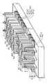
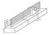
- FIG. 1is a schematic configuration diagram of a nonvolatile semiconductor memory device 9 according to an embodiment of the present invention.
- silicon layers 3 and insulating layers 4are alternately laminated in the manner of 3 a, 4 a, 3 b, 4 b, and 3 c with an insulating film 2 interposed therebetween.
- the insulating film 5is laminated on the silicon layer 3c.
- the silicon layer 3has a configuration having three layers 3a, 3b, and 3c.
- the present inventionis not limited to this, and the larger the number, the larger the memory capacity as a storage device. Therefore, it is preferable.
- the insulating layer 4also increases or decreases with the number of silicon layers 3.
- the insulating film 2is formed of, for example, a silicon oxide film (SiO 2 ), and the silicon layer 3 may be in an amorphous state or a polycrystalline state, but a single crystal state is desirable.
- SiO 2silicon oxide film
- the insulating layer 4is formed of, for example, a silicon oxide film (SiO 2 ), but may be another insulating film as long as the silicon (Si) layer 3 can be electrically insulated.
- the insulating film 5is formed of, for example, a silicon oxide film, but may be another insulating film such as a silicon nitride film (SiN x ) or a structure in which they are stacked.
- SiN xsilicon nitride film
- the laminated film 6 (X)is formed so as to surround a laminated structure composed of a laminated film of the insulating film 2, the silicon layer 3, the insulating layer 4, and the insulating film 5.
- Xis a natural number of 1 to n, and each of the n laminated films 6 is formed in an electrically insulated state.
- the laminated film 6includes an insulating film 6 (X) a, a charge storage layer 6 (X) b, an insulating film 6 (X) c, and an electrode 6 (X) d.
- the state of being electrically insulatedindicates that at least the electrodes 6 (X) d are electrically insulated.
- all of the stacked films 6are independent, but any one of the insulating film 6 (X) a, the charge storage layer 6 (X) b, the insulating film 6 (X) c, or all of them. May be connected.
- the insulating film 6 (X) ais formed of, for example, a silicon oxide film (SiO 2 ).
- the charge storage layer 6 (X) bis formed of, for example, a silicon nitride film (Si 3 N 4 ).
- the insulating film 6 (X) cis formed from, for example, a silicon oxide film (SiO 2 ).
- the electrode 6 (X) dis formed of, for example, nickel silicide (NiSi).
- This laminated structurein which an insulating film 6 (X) a, a charge storage layer 6 (X) b, an insulating film 6 (X) c, and an electrode 6 (X) d are laminated on the silicon layer 3
- the channelthe insulating film 6 (X) a is a tunnel film
- the charge storage layer 6 (X) bis a charge storage layer
- the insulating film 6 (X) cis a block insulating film
- the electrode 6 (X) dis controlled.
- a memory cell of a double gate(a structure in which control gates are arranged on both sides of the silicon layer 3) as a gate is formed.
- each of the laminated films 6 (X)is electrically insulated, and has a single memory string structure as a whole.
- a plurality of silicon layers 3are stacked, and each silicon layer 3 can be controlled as an independent memory string channel. It has a structure laminated on.
- the insulating film 6 (X) acan be used by appropriately selecting a material necessary for each generation of nonvolatile semiconductor memory devices.
- a silicon oxynitride film, a combination of a silicon oxide film and a silicon nitride film, or the likecan be given.
- a material in which silicon nanoparticles or metal ions are mixed with these filmsis also effective, or a combination of these materials may be used.
- charge storage layer 6 (X) bcan be used by appropriately selecting materials necessary for each generation of nonvolatile semiconductor memory devices.
- a material in which the composition ratio of silicon and nitrogen, which are constituent elements such as a hafnium oxide film (HfO 2 ) and a silicon nitride film (SiN), is changed, and silicon nanoparticles and metal A material mixed with ions is also effective, or a combination of these materialsmay be used.
- a semiconductor layersuch as a silicon layer may be used.
- the insulating film 6 (X) ccan be used by appropriately selecting materials necessary for each generation of nonvolatile semiconductor memory devices.
- the composition ratio of the silicon oxide film, the aluminum oxide film (Al 2 O 3 ), the lanthanum aluminum oxide film (LaAlO 3 ), the lanthanum aluminum silicon oxide film (LaAlSiO) and their constituent elementscan be changed. good.
- the electrode 6 (X) dcan be used by appropriately selecting a material necessary for each generation of nonvolatile semiconductor memory devices.
- TaNtantalum nitride
- TaCtantalum carbide
- TiNtitanium nitride
- V, Cr, Mn, Y, Mo, Ru, Rh, Hf, Ta, W, Ir, Co, Ti, Er, Pt, Pd, Zr, Gd, Dy, Howhich show metallic electrical conduction characteristics , Er and their various silicides.
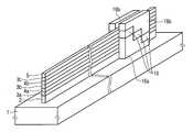
- a plurality of layer selection transistors 10 and selection transistors 11 made of 10a, 10b, and 10care formed in parallel with the laminated film 6 (X).
- the layer selection transistor 10 and the selection transistor 11are drawn in the same structure as the stacked film 6 (X), but any structure may be used as long as the transistor operates with the silicon layer 3 as a channel.
- the layer selection transistor 10may have a structure different from that of the memory cell, for example, a MOS (Metal-Oxide-Semiconductor) transistor including one insulating film and one gate electrode.
- MOSMetal-Oxide-Semiconductor
- each silicon layer 3has an impurity-added region in which the layer selection transistor 10 is always on (normally on). This is applied to a partial region 13 of the channel portion.
- the channel region 13a of the layer selection transistor 10ain the silicon layer 3a, in the channel region 13a of the layer selection transistor 10a, in the silicon layer 3b, in the channel region 13b of the layer selection transistor 10b, and in the silicon layer 3c, the channel region 13c of the layer selection transistor 10c.
- impuritiesare added respectively.
- an impurity that becomes an N-type semiconductorfor example, a pentavalent element such as arsenic (As) phosphorus (P), or an impurity that becomes a P-type semiconductor, for example, boron (B) indium (In) It is also possible to use a combination of these materials.
- a pentavalent elementsuch as arsenic (As) phosphorus (P)
- an impurity that becomes a P-type semiconductorfor example, boron (B) indium (In) It is also possible to use a combination of these materials.
- Each silicon layer 3(memory string) is controlled by a layer selection transistor 10 that can be turned on / off, for example, a layer selection transistor 10 in which no impurity is added to the channel.
- a layer selection transistor 10in which no impurity is added to the channel.
- an impurity for threshold controlmay be added to the channel of the layer selection transistor 10 that can be controlled on / off.
- the silicon layer 3ais controlled by the layer selection transistors 10b and 10c
- the silicon layer 3bis controlled by the layer selection transistors 10a and 10c
- the silicon layer 3cis controlled by the layer selection transistors 10a and 10b.
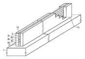
- the electrodes for making contacts that are conventionally formed independently on each memory string layerare all silicon as electrodes 7 and 8 as represented by FIG. It is only necessary to form only one layer 3 that can be contacted in common.
- the increase in the length of the memory stringis only in the region where the layer selection transistor 10 is formed for each layer. Therefore, each time the memory strings are stacked, the contact electrode and the selection transistor are added.
- the lengthcan be shortened compared with the conventional structure formed.
- metal materialssuch as aluminum (Al) can be cited in addition to tungsten (W).
- the number of contact electrodesincreases as the number of memory strings increases as in the conventional case. If it increases, the number of wires drawn from each of them and the circuit area for controlling them will increase.
- the present inventionsince the number of contact electrodes does not increase with each increase in the memory string, it is possible to suppress the increase corresponding to the increase of one layer selection transistor 10 with each increase. The area can be reduced.
- each memory stringcan be controlled, the structure is not limited to that shown in FIG. 2, and can be modified as appropriate.
- a plurality of impurity-added regions 13may exist in the silicon layer 3, or as shown in FIG. 11, are formed on both sides so as to sandwich the laminated film 6 (X). May be.
- the number of layer selection transistors 10does not have to be the same as the number of silicon layers 3, and the number may be large or small as long as each memory string can be controlled. .
- the layer selection transistoris arranged so as to sandwich the memory string, the influence of the diffusion of the impurity-added region 13 can be minimized.
- 4A to 4Fshow a manufacturing process of the nonvolatile semiconductor memory device 9 according to an embodiment of the present invention, in particular, a process of forming the impurity added region 13 in the silicon layer 3.
- a p-type (first conductivity type) silicon substrate 1 having a plane orientation (100) and a specific resistance of 10 to 20 ⁇ cmis prepared, and a silicon oxide film layer is formed on the silicon substrate 1.
- the silicon layer 3 ais laminated by, for example, deposition.
- patterningis performed to provide openings in the resist applied by a photo etching process (Photo Etching Process, hereinafter referred to as “PEP”, a so-called photolithographic lithography process), and ion implantation is performed.
- PEPPhoto Etching Process
- ion implantationis performed.
- an impurity added region 13ais formed in the silicon layer 3a.
- the silicon layer 3bis laminated through the silicon oxide film layer 4a, and the impurity added region 13b is formed by performing patterning by PEP and ion implantation.
- the silicon layer 3cis laminated through the silicon oxide film layer 4b, and patterning by PEP and ion implantation are performed to form the impurity added region 13c.
- the silicon oxide film layer 5is laminated on the silicon layer 3c. This state is shown in FIG. 4B.
- silicon oxide film layer 2silicon layer 3a, silicon oxide film layer 4a, silicon layer 3b, silicon oxide film layer 4b, silicon layer 3c, and insulating film 5 on the silicon substrate 1, for example, by PEP.
- anisotropic dry etchingit is processed into a strip (fin) shape as shown in FIG. 4C.
- the silicon oxide film 106ais formed by performing thermal oxidation.
- the silicon oxide film 106acan also be formed by deposition.
- a tunnel insulating film material necessary for each generation of nonvolatile semiconductor memory devicescan be appropriately selected and used.
- a charge storage layer 106b, an insulating film 106c, and an electrode 106dare deposited. This state is shown in FIG. 4D.
- the silicon oxide film 106a, the charge storage layer 106b, the insulating film 106c, and the electrode 106dare subjected to anisotropic dry etching after patterning using, for example, PEP, and the structure shown in FIG. Then, the laminated film 6 (X), the layer selection transistor 10 and the selection transistor 11 which are electrically insulated from each other are formed.
- the layer selection transistor 10needs to be formed at a position where the corresponding doped region 13 becomes a channel.
- a silicon oxide filmis entirely embedded and subjected to chemical mechanical polishing (CMP), thereby processing the laminated film 6 (X), the layer selection transistor 10, the selection transistor 11, and a fin shape.
- CMPchemical mechanical polishing
- An interlayer insulating film that fills the space between the silicon oxide film layer 2, silicon layer 3a, silicon oxide film layer 4a, silicon layer 3b, silicon oxide film layer 4b, silicon layer 3c, and insulating film 5 on the silicon substrate 1Form.
- anisotropic dry etchingis performed to form a hole pattern in a region where the electrodes 7 and 8 are formed. Thereafter, for example, after depositing tungsten, tungsten other than the hole pattern is subjected to CMP to form the electrodes 7 and 8, and the nonvolatile semiconductor memory device 9 of FIG. 1 is formed.
- FIGS.Although not particularly illustrated, other embodiments can be formed by changing a part thereof.
- patterning by PEPis performed so that the impurity added region 13 shown in FIG. 11 is formed.
- the patterning by PEPis changed and processed so that the length of the fin is increased by the increase of the layer selection transistor, and thereafter, shown in FIG. 4E.
- the patterning by PEPmay be changed so as to have the structure of FIG.
- PEPis required to form each impurity-added region, but rough PEP is sufficient as compared with PEP for contact processing, and it is possible to reduce production costs and to process into a complicated shape. Easy to form. Moreover, since the processing depths of the electrode 7 and the electrode 8 may be equal, both can be formed simultaneously. From the above points, the structure is more effective than the conventional one.
- 5A to 5Cshow a manufacturing process of the nonvolatile semiconductor memory device 9 according to an embodiment of the present invention, particularly, a process of forming the impurity added region 13 in the silicon layer 3.
- a p-type (first conductivity type) silicon substrate 1 having a plane orientation (100) and a specific resistance of 10 to 20 ⁇ cmis prepared, and a silicon layer is formed on the silicon substrate 1 via a silicon oxide film layer 2.
- 3a, the silicon oxide film layer 4a, the silicon layer 3b, the silicon oxide film layer 4b, and the silicon layer 3care alternately stacked by, for example, deposition, and the insulating film 5 is formed on the silicon layer 3 on the outermost surface, for example. , Formed by deposition. This state is shown in FIG. 5A.
- resist patterningis performed by PEP, and ion implantation is performed to form an impurity added region 13a in the silicon layer 3a. This state is shown in FIG. 5B.
- an impurity added region 13bis formed in the silicon layer 3b and an impurity added region 13c is formed in the silicon layer 3c by patterning using PEP and ion implantation, respectively.
- the impurity-added regions 13a, 13b, and 13care formed by changing the depth by changing the energy of ions to be implanted. This state is shown in FIG. 5C.
- the non-volatile semiconductor memory device 9 of FIG. 1is formed by forming in the same procedure as the process described above with reference to FIGS. 4C to 4F.
- FIGS.Although not particularly illustrated, other embodiments can be formed by changing a part thereof.
- patterning by PEPis performed so that the impurity added region 13 shown in FIG. 11 is formed.
- the patterning by PEPis changed and processed so that the length of the fin is increased by the increase of the layer selection transistor, and thereafter, shown in FIG. 4E.
- the patterning by PEPmay be changed so as to have the structure of FIG.
- the silicon layer 3can be formed continuously, and since the resist does not come into contact with the silicon layer 3, the silicon layer 3 is not contaminated, thereby serving as a channel. Characteristic deterioration can be suppressed.
- Impuritiesmay be added in the region immediately above the impurity addition region 13a in 3c.
- 6A to 6Cshow a manufacturing process of the nonvolatile semiconductor memory device 9 according to one embodiment of the present invention, in particular, a process of forming the impurity added region 13 in the silicon layer 3.
- a p-type (first conductivity type) silicon substrate 1 having a plane orientation (100) and a specific resistance of 10 to 20 ⁇ cmis prepared, and a silicon oxide film layer is formed on the silicon substrate 1.
- the silicon layer 3a, the silicon oxide film layer 4a, the silicon layer 3b, the silicon oxide film layer 4b, and the silicon layer 3care alternately stacked by, for example, deposition.
- the insulating film 5is formed by deposition, for example.
- silicon oxide film layer 2silicon layer 3a, silicon oxide film layer 4a, silicon layer 3b, silicon oxide film layer 4b, silicon layer 3c, and insulating film 5 on the silicon substrate 1, for example, by PEP.
- anisotropic dry etchingit is processed into a fin shape as shown in FIG. 6A.
- a silicon oxide filmis deposited and subjected to anisotropic dry etching after patterning by, for example, PEP, so that it has a step shape and is processed into a fin shape as indicated by 15 in FIG. 6B.
- the laminated filmsilicon oxide film layer 2, silicon layer 3a, silicon oxide film layer 4a, silicon layer 3b, silicon oxide film layer 4b, silicon layer 3c, insulating film 5 on silicon substrate 1.
- each of the staircase shapesis preferably located below the upper ends of the silicon layers 3a, 3b, and 3c.
- a silicon oxide film to which an impurity added for forming the impurity-added region 13 is addedis deposited.
- anisotropic dry etchingis performed, which is indicated by 16 in FIG. 6C.
- the silicon oxide film 15is processed into a shape that is formed on each step shape.
- the height of 16is preferably located below the upper ends of the silicon oxide films 4a and 4b and the insulating film 5 formed on the silicon layer 3 in contact with each other.
- impuritiesare solid-diffused from the impurity-added silicon oxide film 16 to the silicon layer 3 to which the impurity-added silicon oxide film 16 is in contact, and the impurity-added region 13 is formed.
- the nonvolatile semiconductor memory device 9 shown in FIGS. 1 and 2is formed by forming in the same procedure as the process described above with reference to FIGS. 4D to 4F.
- a silicon oxide film layer 2a silicon layer 3a, a silicon oxide film layer 4a, a silicon layer 3b, a silicon oxide film layer 4b, a silicon layer 3c, and an insulating film 5 are laminated on the silicon substrate 1, respectively, for example, by PEP After patterning, it is processed into a fin shape by performing anisotropic dry etching.
- an impurity-added silicon oxide filmis deposited and subjected to anisotropic dry etching after patterning by, for example, PEP, thereby having a step shape and a fin shape as shown by 16a in FIG. 9A.
- the laminated filmsilicon oxide film layer 2, silicon layer 3a, silicon oxide film layer 4a, silicon layer 3b, silicon oxide film layer 4b, silicon layer 3c, insulating film 5 on the silicon substrate 1. Process into shape.
- each of the staircase shapesis preferably located below the upper ends of the silicon layers 3a, 3b, and 3c.
- a silicon oxide filmis deposited and subjected to anisotropic dry etching after patterning by, for example, PEP, so that each of the stepped shapes of the impurity-added silicon oxide film 16a is shown as 15 in FIG. 9B. Process into a shape that will be formed on top.
- the height of 15is preferably located below the upper ends of the silicon oxide films 4a and 4b and the insulating film 5 formed on the silicon layer 3 in contact with each other.
- an impurity-added silicon oxide filmis deposited and formed on each of the silicon oxide films 15 as shown by 16b in FIG. 9C by performing anisotropic dry etching after patterning by PEP, for example. It is processed into a shape as
- impuritiesare solid-diffused from the doped silicon oxide films 16 a and 16 b to the silicon layer 3 in contact with the doped silicon oxide films 16 a and 16 b, respectively. Region 13 is formed.
- the nonvolatile semiconductor memory device 9 shown in FIGS. 1 and 8is formed by forming in the same procedure as the process described above with reference to FIGS. 4D to 4F.
- FIGS. 6A to 6Cshow a manufacturing process of the nonvolatile semiconductor memory device 9 which is partly different from FIGS. 6A to 6C.
- a silicon oxide film layer 2a silicon layer 3a, a silicon oxide film layer 4a, a silicon layer 3b, a silicon oxide film layer 4b, a silicon layer 3c, and an insulating film 5 are laminated on the silicon substrate 1, respectively, for example, by PEP After patterning, it is processed into a fin shape by performing anisotropic dry etching.
- a silicon oxide filmis deposited and, for example, patterned by PEP, and then subjected to anisotropic dry etching so that it has a step shape and is processed into a fin shape as indicated by 15 in FIG. 7A.
- a shape as to come into contact with the laminated filmsilicon oxide film layer 2, silicon layer 3a, silicon oxide film layer 4a, silicon layer 3b, silicon oxide film layer 4b, silicon layer 3c, insulating film 5 on silicon substrate 1 Process.
- each of the staircase shapesis preferably located below the upper ends of the silicon layers 3a, 3b, and 3c.
- the silicon insulating film layer 15as shown in FIG. 7A, as shown in FIG. 7B, when the subsequent doped silicon oxide film layer 16 is formed, it can be formed only by deposition. Since the process such as PEP can be omitted, the manufacturing cost can be reduced.
- impuritiesare solid-diffused from the doped silicon oxide film 16 to the silicon layer 3 to which the doped silicon oxide film 16 is in contact, respectively.
- An impurity added region 13is formed.
- the nonvolatile semiconductor memory device 9 shown in FIGS. 1 and 2is formed by forming in the same procedure as the process described above with reference to FIGS. 4D to 4F.
- 10A and 10Bshow a manufacturing process of the nonvolatile semiconductor memory device 9 which is partly different from FIGS. 9A to 9D.
- a silicon oxide film layer 2a silicon layer 3a, a silicon oxide film layer 4a, a silicon layer 3b, a silicon oxide film layer 4b, a silicon layer 3c, and an insulating film 5 are laminated on the silicon substrate 1, respectively, for example, by PEP After patterning, it is processed into a fin shape by performing anisotropic dry etching.
- an impurity-added silicon oxide filmis deposited and subjected to anisotropic dry etching after patterning by, for example, PEP, thereby having a step shape and a fin shape as shown by 16a in FIG. 10A.
- the laminated filmsilicon oxide film layer 2, silicon layer 3a, silicon oxide film layer 4a, silicon layer 3b, silicon oxide film layer 4b, silicon layer 3c, insulating film 5 on the silicon substrate 1. Process into shape.
- each of the staircase shapesis preferably located below the upper ends of the silicon layers 3a, 3b, and 3c.
- each of the stepped shapes of the doped silicon oxide film 16ais obtained. It is processed into a shape that covers the upper and other laminated fin structures.
- the height 15 formed on the impurity-added silicon oxide film layer 16ais higher than the upper ends of the silicon oxide films 4a and 4b and the insulating film 5 formed on the silicon layer 3 in contact with each other. It is desirable to be located below.
- the silicon insulating film layer 15into a shape as shown in FIG. 10A, it is possible to form the silicon oxide film layer 16b only by deposition when forming the subsequent doped silicon oxide film layer 16b as shown in FIG. 10B.
- the process such as PEPcan be omitted, the manufacturing cost can be reduced.
- impuritiesare solidified from the doped silicon oxide films 16a and 16b to the silicon layer 3 in contact with the doped silicon oxide films 16a and 16b. Layer diffusion is performed, and an impurity-added region 13 is formed.
- the nonvolatile semiconductor memory device 9 shown in FIGS. 1 and 8is formed by forming in the same procedure as the process described above with reference to FIGS. 4D to 4F.
- FIG. 10AFrom the structure of FIG. 10A, a structure similar to FIG. 9D can be formed without forming the structure of FIG. 10B.
- the positional relationship of the impurity-added region 13is such that the impurity-added silicon oxide films 16, 16a, 16b is determined by the shape of each of the regions 16b, and in the case of forming by the method shown in FIGS. 4A to 4F and FIGS. 5A to 5C, when patterning by PEP for ion implantation, the positional relationship between the regions is PEP. It is possible to avoid the problem of being unable to maintain due to the accuracy of
- the silicon oxide film 15 and the impurity-added silicon oxide films 16 and 16a16bare formed so as to sandwich both sides of the fin shape. Although formed, it is possible even when formed only on one side. However, when using vapor phase diffusion, it is necessary to cover the other side with an arbitrary layer that does not cause unintended solid phase diffusion to the silicon layer 3.
- FIGS. 6A to 6C, FIGS. 7A and 7B, FIGS. 9A to 9D, and FIGS. 10A and 10Buse a silicon oxide film, but the material is not limited to this, and impurities can be diffused into a solid layer. If it is material, there will be no restriction
- 12A and 12Bare cross-sectional views of the nonvolatile semiconductor memory device according to the embodiment of the present invention.
- FIG. 12Ashows a structure in which a selection transistor 11b is further added to the structure shown in FIG.
- Such a structureimproves the cut-off characteristics of the memory string and can suppress malfunction. In that case, the effect can be obtained by further adding a selection transistor 11c as shown in FIG. 12B.
- FIG. 13is a cross-sectional view of a nonvolatile semiconductor memory device according to an embodiment of the present invention.
- the silicon layer 3is interrupted in the respective impurity-added regions 13, and the insulating films 4a, 4b, and 5 stacked on each of the silicon layers 3 are different from each other.
- the silicon layer 3is interrupted immediately above each of the impurity-added regions 13, and the interrupted region is the silicon layer 14.
- the silicon layers 3are connected to each other by another silicon layer 14 different from the silicon layers 3 through the impurity addition regions 13.
- the string of the channel portion of the layer selection transistorbecomes thicker and the electrical resistance is correspondingly reduced. Therefore, the layer selection is faster than the structure of FIG. 2, and the memory cell can be operated at high speed. .
- the impurity addition region 13is provided in the channel of the layer selection transistor closest to the memory string in the silicon layer 3c, and makes the layer selection transistor uncontrollable.
- the impurity addition region 13is provided in the channel of the layer selection transistor that is second closest to the memory string, and makes the layer selection transistor uncontrollable.
- the impurity added region 13is provided in the channel of the layer selection transistor farthest from the memory string in the silicon layer 3a, and makes the layer selection transistor uncontrollable.
- a p-type (first conductivity type) silicon substrate 1 having a plane orientation (100) and a specific resistance of 10 to 20 ⁇ cmis prepared, and a silicon layer is formed on the silicon substrate 1 via a silicon oxide film layer 2.
- 3a, the silicon oxide film layer 4a, the silicon layer 3b, the silicon oxide film layer 4b, and the silicon layer 3care alternately stacked by, for example, deposition, and the insulating film 5 is formed on the silicon layer 3 on the outermost surface, for example. , Formed by deposition.
- a part of the laminated film composed of the silicon oxide film layer 2, the silicon layer 3a, the silicon oxide film layer 4a, the silicon layer 3b, the silicon oxide film layer 4b, the silicon layer 3c, and the insulating film 5 on the silicon substrate 1is As shown in FIG. 14A, a stepped shape in which the silicon layer 3 is partially exposed is processed by performing anisotropic dry etching after patterning by PEP, for example.
- an impurity added region 13is formed in the exposed portion of the silicon layer 3 by ion implantation. This state is shown in FIG. 14B. At this time, if necessary, patterning by PEP that opens only the impurity-added region 13 may be performed.
- siliconis deposited, and a silicon layer 14 is formed by performing a planarization process by CMP, for example.
- the planarization of the silicon layer 14can also be formed by dry etching.
- siliconmay be epitaxially grown on the impurity-added region 13 to form a single crystal state. If the silicon layer is in a polycrystalline state, a current flows through the crystal grain boundary and the off characteristics of the layer selection transistor 10 are deteriorated. Therefore, the silicon layer 14 is preferably in a single crystal state. Further, an insulating film may be formed on the silicon layer 14 to protect the silicon layer 14.
- the laminated structure shown in FIG. 14Cis processed into a fin shape as shown in FIG. 14D.
- FIG. 14Eis obtained by forming in the same procedure as described above with reference to FIGS. 4D to 4F, and the nonvolatile semiconductor memory device 9 shown in FIG. It is formed.
- FIG. 15is a cross-sectional view of a nonvolatile semiconductor memory device according to an embodiment of the present invention.
- FIG. 2is different from the structure shown in FIG. 2 in that an impurity-added silicon 17 is formed around an electrode 7 for contact with a memory string.
- the electrode 7is connected to the bit line
- the electrode 8is connected to the source line
- the impurity-added region 13 and the impurity-added silicon 17 in the silicon layer 3are n + -type, respectively.
- the constituent element of the p-type semiconductormay be replaced with an n-type semiconductor, and the constituent element of the n-type semiconductor may be replaced with a p-type semiconductor.
- a large positive biasis applied to the memory cell to be written, for example, the control gate 6 (3) d of the memory cell 6 (3) to inject electrons into the charge storage layer 6 (3) b of the memory cell 6 (3). And write.
- a negative biasmay be applied to a memory cell that is not desired to be written, for example, 6 (X) control gate 6 (X) d other than 6 (3).
- a p-type accumulation regionis generated in the silicon layers 3a, 3b, and 3c serving as memory string channels.
- a large negative biasis applied to the memory cell to be erased, for example, the control gate 6 (2) d of the memory cell 6 (2), and holes are formed in the charge storage layer 6 (2) b of the memory cell 6 (2). Inject and erase.
- a positive biasmay be applied to a memory cell that is not desired to be erased, for example, a control gate 6 (X) d of 6 (X) other than the memory cell 6 (2).
- the source line contact electrode 7is grounded and a positive bias is applied to the bit line contact electrode 8 to read the memory cell, for example, a memory other than the memory cell 6 (1), as in a normal NAND flash memory.
- a positive biasis applied to the control gate 6 (X) d of the cell 6 (X), and reading is performed as information “0” or “1” depending on whether or not a current flows.
- the memory strings stacked by the bias application method of the layer selection gates 10a, 10b, and 10ccan be selected and read out.
- the above operationcan be performed in the same manner as in this embodiment.
- the source resistance due to the Schottky barriermay significantly reduce the current flowing during reading. Incidentally, such a Schottky barrier does not cause a problem on the drain region side, and thus the above-described problem does not occur in this embodiment.
- the same effectcan be obtained even if the electrode 8 is formed of a metal material and the electrode 7 is formed of impurity-doped silicon.
- the impurity-doped silicon 17is provided around the electrode 7. May not be formed.
- 16A and 16Bare schematic configuration diagrams of the silicon layer 3 particularly surrounded by the laminated film 6 in the nonvolatile semiconductor memory device 9 according to the embodiment of the present invention.
- the silicon layers 3a, 3b, and 3chave air gaps 18a, 18b, and 18c, respectively, in the portions surrounded by the laminated film 6.
- the air gaps 18a, 18b and 18care formed in the insulating films 4a, 4b and 5.
- the air gaps 18a, 18b, and 18cmay be formed not only in the portion surrounded by the laminated film 6, but also in the portion surrounded by the layer selection transistor 10 and the selection transistor 11, and further, the silicon layers 3a, You may spread to the whole between 3b and 3c.
- the relative dielectric constant between the silicon layers 3a, 3b, and 3cbecomes low, and the same insulation characteristics can be obtained even if the gap between them is narrowed.
- the space between the silicon layers 3a, 3b, 3ccan be narrowed, and the degree of integration can be increased.
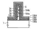
- 18A to 18Hshow a manufacturing process of the nonvolatile semiconductor memory device according to one embodiment of the present invention, in particular, a forming process of the insulating layer 18 including an air gap in the silicon layer 3.
- a p-type (first conductivity type) silicon substrate 1 having a plane orientation (100) and a specific resistance of 10 to 20 ⁇ cmis prepared, and silicon germanium (SiGe) is formed on the silicon substrate 1.
- the silicon layer 3 and the silicon germanium layer 104are alternately stacked so as to be 3a, 104a, 3b, 104b, and 3c through the layer 102.
- silicon and silicon germaniumcan be epitaxially grown by depositing and growing a crystal film while maintaining a crystallographic orientation relationship with the silicon substrate 1, the silicon layer 3 and the silicon germanium layer 104 should be formed of a single crystal. Can do.
- An insulating film 5is formed on the outermost silicon layer 3 by, for example, deposition. This state is shown in FIG. 18B.
- a stacked structure including the silicon germanium layer 102, the silicon layer 3a, the silicon germanium layer 104a, the silicon layer 3b, the silicon germanium layer 104b, the silicon layer 3c, and the insulating film 5 on the silicon substrate 1is patterned by, for example, PEP. Thereafter, anisotropic dry etching is performed to form a strip shape as shown in FIG. 18C.
- the silicon oxide film 106ais formed by performing thermal oxidation.
- a silicon germanium oxide filmis formed on the silicon germanium layers 102 and 104.
- This silicon oxide film 106acan also be formed by deposition.
- a tunnel insulating film material necessary for each generation of nonvolatile semiconductor memory devicescan be appropriately selected and used.
- a charge storage layer 106b, an insulating film 106c, and an electrode 106dare deposited.
- the silicon oxide film 106a, the charge storage layer 106b, the insulating film 106c, and the electrode 106dare subjected to anisotropic dry etching after patterning by, for example, PEP, and are shown in FIG. Then, the laminated film 6 (X), each of which is electrically insulated, is formed.
- the silicon germanium layers 102 and 104are shown to be surrounded by the laminated film 6 (X), but actually, between the laminated films 6 (X), There is a void, and the silicon germanium layers 102 and 104 are etched from the void.
- a silicon oxide filmis deposited on the entire surface, and the silicon oxide film 2 and the silicon oxide film 4 are formed in the region where the silicon germanium layers 102 and 104 are removed.
- the silicon oxide film 2 and the silicon oxide film 4do not need to be entirely formed of a silicon oxide film.
- the air gapmay be in a state where a part or no silicon oxide film is formed.
- the space surrounded by the laminated film 6 (X), the layer selection transistor 10 and the selection transistor 11is not preferentially embedded, and air Insulating layers 18a, 18b, 18c including gaps are formed.
- anisotropic dry etchingis performed to form a hole pattern in a region where the electrodes 7 and 8 are to be formed.
- the electrodes 7 and 8are formed by CMP of tungsten other than the hole pattern, and the nonvolatile layer including the insulating layer 18 including the air gap shown in FIGS. 16A and 16B is formed.
- a semiconductor memory device 9is formed.
- FIG. 17is a schematic configuration diagram of the nonvolatile semiconductor memory device 9 according to one embodiment of the present invention.
- An erasing electrode 19is formed on the memory cell, and a bias is applied to the erasing electrode 19 during the erasing operation of the memory cell composed of the laminated film 6 (X), whereby a hole is formed in the charge storage layer 6 (X) b of the memory cell. It is a structure that can be injected and operated.
- the fringe electric field from the erasing electrode 19 toward the insulating layer 18is weakened when a bias is applied to the erasing electrode 19.
- the concentration of the electric field on each silicon layer 3can be improved.
- the formation method of the embodimentis not limited, and for example, the formation method by epitaxial growth of SiGe and Si shown in FIG. 18 may be used for the purpose of forming a channel with Si single crystal.
- siliconis used as the substrate, but other substrates such as a germanium substrate can also be used.
- the diffusion layer region between each of the memory cell composed of the laminated film 6 (X) in the silicon layer 3, the selection transistor 11, and the layer selection transistors 10a, 10b, and 10cis not described. What is necessary is just to form.
- an electric field(fringe electric field) is applied not only directly below the laminated film 6 (X) but also to the silicon layer 3 between the laminated films 6 (X).
- 6 (X) intervalis short, for example, 30 nm or less, the current path passes through the channel only with the fringe electric field (for example, Chang-Hyum Lee, et al, VLSI Technology Digest of Technical Papers, pp118- 119, 2008), the diffusion layer may not be formed.
- the source line and the bit lineare common to each of the stacked strings, and even if the memory strings are stacked, the increase in length forms a layer selection transistor for each layer. Therefore, the length can be shortened as compared with the conventional structure. Similarly, the number of wirings and the circuit area can be suppressed to an increase corresponding to the increase of one layer selection transistor for each layer.
- the present inventionrelates to a file memory capable of high-speed random writing, a portable terminal capable of high-speed download, a portable player capable of high-speed download, a semiconductor memory for broadcasting equipment, a drive recorder, a home video, a large-capacity buffer memory for communication, and a semiconductor memory for security camera
- a file memory capable of high-speed random writinga portable terminal capable of high-speed download
- a portable player capable of high-speed downloada semiconductor memory for broadcasting equipment, a drive recorder, a home video, a large-capacity buffer memory for communication, and a semiconductor memory for security camera
- the industrial meritis great.
- SYMBOLS 1Silicon (Si) substrate (semiconductor substrate), 2 ... Silicon oxide film (SiO2), 3 (3a, 3b, 3c) ... Silicon layer (memory string channel region), 4 (4a, 4b) ... Silicon oxide film ( (Memory string insulating region), 5 ... silicon oxide film, 6 (X) ... laminated film (X is a natural number of 1 to n), 6 (X) a ... silicon oxide film (memory cell tunnel insulating film), 6 (X) b ... silicon nitride film (Si 3 N 4 ) (memory cell charge storage layer), 6 (X) c ...
- Nonvolatile semiconductor memory device10 (10 a, 10b, 10c) ... layer selection transistor, 11, 11b, 11c ... selection transistor, 13 (13a, 13b, 13c) ... impurity doped region in the silicon layer 3, 14 ... silicon layer, 15 ... silicon oxide film, 16, 16a, 16b ... impurity doped silicon oxide film, 17 ... impurity doped silicon (diffusion layer region), 18 (18a, 18b, 18c) ...
- insulating layerincluding air gap, 19 ... erasing electrode, 102 ... silicon germanium (SiGe) 104, 104a, 104b, silicon germanium layer, 106a, silicon oxide film, 106b, silicon nitride film, 106c, silicon oxide film, 106d, nickel silicide.
- SiGesilicon germanium
Landscapes
- Semiconductor Memories (AREA)
- Non-Volatile Memory (AREA)
Abstract
Description
Translated fromJapanese本発明は、電気的にデータの書き換えが可能な不揮発性半導体記憶装置に関する。The present invention relates to a nonvolatile semiconductor memory device capable of electrically rewriting data.
NAND型フラッシュメモリの高集積化、大容量化を進めるためには、デザインルールを縮小することが必要となる。このデザインルールを縮小するためには、配線パターン等の更なる微細加工が必要となる。配線パターン等の更なる微細加工を実現するためには、非常に高度な加工技術が要求されるため、結果としてデザインルールの縮小化が困難になってきている。In order to increase the integration density and capacity of NAND flash memory, it is necessary to reduce the design rule. In order to reduce this design rule, further fine processing such as a wiring pattern is required. In order to realize further fine processing of wiring patterns and the like, a very advanced processing technique is required, and as a result, it is difficult to reduce the design rule.
そこで、近年、メモリの集積度を高めるために、メモリセルを3次元的に配置した半導体記憶装置が、例えば、特許文献1~4に提案されている。Therefore, in recent years, for example,
これら特許文献1~4に開示されている不揮発性半導体記憶装置は、積層されたアクティブエリアを一括加工で形成し、ゲートコンタクトも一括形成すると共に、積層された各メモリストリングを階層選択トランジスタで一括選択する方式で形成することによりチップ面積の縮小化を実現し、メモリの集積度を高めることができる構造である。また、積層構造を一括形成できることで製造にかかるコストを大幅に抑制することが可能となる。In these nonvolatile semiconductor memory devices disclosed in
しかし、この構造においても、メモリストリング一層ごとに階層選択のためのトランジスタ及びコンタクトプラグを形成しているため、それらを形成するための領域が必要となり、結果として積層を増やすごとにメモリストリングが増大してしまう。さらに、積層された各メモリストリングからの配線の引き出しの形成が難しく、或いは配線の引き出しを形成することに伴う配線数及び回路面積の増大が生じてしまい、積層化のメリットが縮小してしまう。However, even in this structure, since the transistors and contact plugs for selecting the hierarchy are formed for each memory string layer, a region for forming them is necessary, and as a result, the memory string increases as the number of layers increases. Resulting in. In addition, it is difficult to form wiring leads from the stacked memory strings, or the number of wirings and the circuit area increase due to the formation of wiring leads, and the merit of stacking is reduced.
現状、これらの問題を解決する不揮発性半導体記憶装置の構造については開示されていない。Currently, there is no disclosure of the structure of a nonvolatile semiconductor memory device that solves these problems.
本発明は、高い集積度を有する不揮発性半導体記憶装置を提供する。The present invention provides a nonvolatile semiconductor memory device having a high degree of integration.
本発明の例に係わる不揮発性半導体記憶装置は、半導体基板と、前記半導体基板の表面に対して垂直な第1方向に積み重ねられ、前記半導体基板の表面に平行な第2方向に延びる第1乃至第nのメモリストリングス(nは2以上の自然数)と、前記第1乃至第nのメモリストリングスのうちの1つを選択する第1乃至第kのレイヤー選択トランジスタ(kは2以上の自然数)とを備える。前記第1乃至第nのメモリストリングスは、前記第1方向に互いに絶縁されて積み重ねられる第1乃至第nの半導体層と、前記第1乃至第nの半導体層の前記第1及び第2方向に垂直な第3方向の側面上に、第1の絶縁膜、電荷蓄積層、第2の絶縁膜及びコントロールゲート電極の順番で、前記第3方向に積み重ねられる第1の積層構造とを有する。前記第1乃至第nのメモリストリングスは、前記第1乃至第nの半導体層をチャネルとし、前記第2方向に直列に接続される電気的に書き換え可能な第1乃至第mのメモリセル(mは2以上の自然数)を有する。前記コントロールゲート電極は、前記第1乃至第nの半導体層に跨って形成される。前記第1乃至第kのレイヤー選択トランジスタは、前記第1乃至第nの半導体層の前記第3方向の側面上に、第3の絶縁膜及び第1のセレクトゲート電極の順番で、前記第3方向に積み重ねられる第2の積層構造を有する。前記第1乃至第kのレイヤー選択トランジスタは、前記第1乃至第nの半導体層をチャネルとし、前記第2方向に直列に接続される。前記第1のセレクトゲート電極は、前記第1乃至第nの半導体層に跨って形成される。前記第1乃至第kのレイヤー選択トランジスタの各々は、前記第1乃至第nの半導体層のうちの少なくとも1つで常時オンの制御不可能状態であり、残りの少なくとも1つの半導体層でオン/オフが可能である制御可能状態である。前記第1乃至第kのレイヤー選択トランジスタの前記第1乃至第nの半導体層での前記制御不可能状態/前記制御可能状態の関係は、互いに異なっている。A nonvolatile semiconductor memory device according to an example of the present invention includes a semiconductor substrate and first to third layers stacked in a first direction perpendicular to the surface of the semiconductor substrate and extending in a second direction parallel to the surface of the semiconductor substrate. N-th memory strings (n is a natural number of 2 or more) and first to k-th layer selection transistors (k is a natural number of 2 or more) for selecting one of the first to n-th memory strings. Is provided. The first to nth memory strings are insulated from each other in the first direction and stacked in the first and nth semiconductor layers, and the first to nth semiconductor layers in the first and second directions. On the side surface in the vertical third direction, the first stacked structure is stacked in the third direction in the order of the first insulating film, the charge storage layer, the second insulating film, and the control gate electrode. The first to nth memory strings are electrically rewritable first to mth memory cells (m) connected in series in the second direction with the first to nth semiconductor layers as channels. Has a natural number of 2 or more. The control gate electrode is formed across the first to nth semiconductor layers. The first to kth layer selection transistors are arranged in the order of a third insulating film and a first select gate electrode on the side surface in the third direction of the first to nth semiconductor layers. A second laminated structure stacked in a direction. The first to kth layer selection transistors are connected in series in the second direction using the first to nth semiconductor layers as channels. The first select gate electrode is formed across the first to nth semiconductor layers. Each of the first to kth layer selection transistors is always in an uncontrollable state in at least one of the first to nth semiconductor layers, and is turned on / off in the remaining at least one semiconductor layer. This is a controllable state that can be turned off. The relationship between the uncontrollable state / the controllable state in the first to nth semiconductor layers of the first to kth layer selection transistors is different from each other.
本発明によれば、高い集積度を有する不揮発性半導体記憶装置を実現できる。According to the present invention, a non-volatile semiconductor memory device having a high degree of integration can be realized.
以下に、本発明の各実施の形態について図面を参照しながら説明する。尚、実施の形態を通して共通の構成には同一の符号を付すものとし、重複する説明は省略する。また、各図は発明の説明とその理解を促すための模式図であり、その形状や寸法、比などは実際の装置と異なる個所があるが、これらは以下の説明と公知の技術を参酌して適宜、設計変更することができる。Hereinafter, embodiments of the present invention will be described with reference to the drawings. In addition, the same code | symbol shall be attached | subjected to a common structure through embodiment, and the overlapping description is abbreviate | omitted. Each figure is a schematic diagram for promoting explanation and understanding of the invention, and its shape, dimensions, ratio, and the like are different from those of an actual device. However, these are in consideration of the following explanation and known techniques. The design can be changed as appropriate.
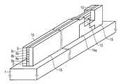
図1は、本発明の一実施形態に係る不揮発性半導体記憶装置9の概略構成図である。FIG. 1 is a schematic configuration diagram of a nonvolatile semiconductor memory device 9 according to an embodiment of the present invention.
シリコン基板(半導体基板)1の主面上には、絶縁膜2を介してシリコン層3と、絶縁層4が、それぞれ、3a、4a、3b、4b、3cのように交互に積層されており、シリコン層3cの上には絶縁膜5が積層されている。On the main surface of the silicon substrate (semiconductor substrate) 1,
尚、本実施形態では、シリコン層3は3a、3b、3cからなる3層を有する構成を示しているが、これに限定されるものではなく多ければ多いほど記憶装置としてのメモリ容量が大きくなるため好ましい。In this embodiment, the
また、絶縁層4もシリコン層3の層数に伴い増減する。Further, the insulating
絶縁膜2は、例えば、シリコン酸化膜(SiO2)で形成されており、シリコン層3は、アモルファス状態、多結晶状態でも良いが、単結晶状態が望ましい。The insulating
絶縁層4は、例えば、シリコン酸化膜(SiO2)で形成されているが、シリコン(Si)層3がそれぞれ電気的に絶縁できる構造であれば、他の絶縁膜でも良い。The insulating
絶縁膜5は、例えば、シリコン酸化膜で形成されているが、シリコン窒化膜(SiNx)などの他の絶縁膜、又はそれらが積層された構造でも良い。The insulating
積層膜6(X)は、絶縁膜2、シリコン層3、絶縁層4、絶縁膜5の積層からなる積層構造の周りを取り囲むように形成されている。ここで、Xは1~nの自然数をとり、n個の積層膜6のそれぞれが電気的に絶縁された状態で形成されている。The laminated film 6 (X) is formed so as to surround a laminated structure composed of a laminated film of the insulating
この積層膜6は、絶縁膜6(X)a、電荷蓄積層6(X)b、絶縁膜6(X)c、電極6(X)dからなっており、前述した、積層膜6のそれぞれが電気的に絶縁された状態とは、少なくとも電極6(X)dがそれぞれ電気的に絶縁されていることを示している。The
従って、図1には、積層膜6のすべてが独立しているが、絶縁膜6(X)a、電荷蓄積層6(X)b、絶縁膜6(X)cのいずれか又はそれらの全てが連結していても良い。Accordingly, in FIG. 1, all of the
絶縁膜6(X)aは、例えば、シリコン酸化膜(SiO2)で形成されている。電荷蓄積層6(X)bは、例えば、シリコン窒化膜(Si3N4)で形成されている。絶縁膜6(X)cは、例えば、シリコン酸化膜(SiO2)から形成されている。電極6(X)dは、例えば、ニッケルシリサイド(NiSi)で形成されている。The insulating film 6 (X) a is formed of, for example, a silicon oxide film (SiO2 ). The charge storage layer 6 (X) b is formed of, for example, a silicon nitride film (Si3 N4 ). The insulating film 6 (X) c is formed from, for example, a silicon oxide film (SiO2 ). The electrode 6 (X) d is formed of, for example, nickel silicide (NiSi).
シリコン層3上に絶縁膜6(X)a、電荷蓄積層6(X)b、絶縁膜6(X)c、電極6(X)dが積層されているこの積層構造は、シリコン層3をチャネルとし、絶縁膜6(X)aをトンネル膜とし、電荷蓄積層6(X)bを電荷蓄積層とし、絶縁膜6(X)cをブロック絶縁膜とし、電極6(X)dをコントロールゲートとしたダブルゲート(シリコン層3の両側にコントロールゲートが配置される構造)のメモリセルを形成している。This laminated structure in which an insulating film 6 (X) a, a charge storage layer 6 (X) b, an insulating film 6 (X) c, and an electrode 6 (X) d are laminated on the
また、積層膜6(X)は、それぞれが電気的に絶縁されており、全体として一本のメモリストリング構造となっている。ここで、図1では、シリコン層3が複数積層されており、さらに、それぞれのシリコン層3は、独立したメモリストリングのチャネルとして制御が可能であるため、図1全体として、メモリストリングを3次元に積層させた構造となっている。Further, each of the laminated films 6 (X) is electrically insulated, and has a single memory string structure as a whole. Here, in FIG. 1, a plurality of
尚、絶縁膜6(X)aは、各世代の不揮発性半導体記憶装置で必要な材料を適宜選択して用いることができる。The insulating film 6 (X) a can be used by appropriately selecting a material necessary for each generation of nonvolatile semiconductor memory devices.
具体的には、シリコン酸窒化膜や、シリコン酸化膜とシリコン窒化膜との組み合わせ等が挙げられる。また、それらの膜に、シリコンナノ粒子や金属イオンを混ぜた材料も有効であるし、それらの材料を組み合わせたものでも良い。Specifically, a silicon oxynitride film, a combination of a silicon oxide film and a silicon nitride film, or the like can be given. In addition, a material in which silicon nanoparticles or metal ions are mixed with these films is also effective, or a combination of these materials may be used.
また、電荷蓄積層6(X)bは、各世代の不揮発性半導体記憶装置で必要な材料を適宜選択して用いることができる。Further, the charge storage layer 6 (X) b can be used by appropriately selecting materials necessary for each generation of nonvolatile semiconductor memory devices.
具体的には、ハフニウム酸化膜(HfO2)や、シリコン窒化膜(SiN)等の構成元素であるシリコン及び窒素の組成比を変化させた材料、及び、それらの膜に、シリコンナノ粒子や金属イオンを混ぜた材料も有効であるし、それらの材料の組み合わせでも良い。或いは、シリコン層などの半導体層でも良い。Specifically, a material in which the composition ratio of silicon and nitrogen, which are constituent elements such as a hafnium oxide film (HfO2 ) and a silicon nitride film (SiN), is changed, and silicon nanoparticles and metal A material mixed with ions is also effective, or a combination of these materials may be used. Alternatively, a semiconductor layer such as a silicon layer may be used.
また、絶縁膜6(X)cは、各世代の不揮発性半導体記憶装置で必要な材料を適宜選択して用いることができる。In addition, the insulating film 6 (X) c can be used by appropriately selecting materials necessary for each generation of nonvolatile semiconductor memory devices.
具体的には、シリコン酸化膜、酸化アルミニウム膜(Al2O3)、ランタンアルミニウム酸化膜(LaAlO3)、ランタンアルミニウムシリコン酸化膜(LaAlSiO)及びそれらの構成元素の組成比を変化させてものでも良い。Specifically, the composition ratio of the silicon oxide film, the aluminum oxide film (Al2 O3 ), the lanthanum aluminum oxide film (LaAlO3 ), the lanthanum aluminum silicon oxide film (LaAlSiO) and their constituent elements can be changed. good.
また、電極6(X)dは、各世代の不揮発性半導体記憶装置で必要な材料を適宜選択して用いることができる。Further, the electrode 6 (X) d can be used by appropriately selecting a material necessary for each generation of nonvolatile semiconductor memory devices.
具体的には、タンタルナイトライド(TaN)、タンタルカーバイト(TaC)、チタンナイトライド(TiN)等のような金属化合物でも同様の効果が得られる。Specifically, the same effect can be obtained with a metal compound such as tantalum nitride (TaN), tantalum carbide (TaC), titanium nitride (TiN), or the like.
さらに、金属的な電気伝導特性を示す、V、Cr、Mn、Y、Mo、Ru、Rh、Hf,Ta、W,Ir、Co、Ti、Er、Pt、Pd、Zr、Gd、Dy、Ho、Er及びそれら種々のシリサイドでも良い。Furthermore, V, Cr, Mn, Y, Mo, Ru, Rh, Hf, Ta, W, Ir, Co, Ti, Er, Pt, Pd, Zr, Gd, Dy, Ho, which show metallic electrical conduction characteristics , Er and their various silicides.
本実施形態では、積層膜6(X)と平行に10a、10b、10cからなる複数のレイヤー選択トランジスタ10及び選択トランジスタ11が形成されている。In this embodiment, a plurality of
図1では、レイヤー選択トランジスタ10及び選択トランジスタ11が積層膜6(X)と同様の構造で描かれているが、シリコン層3をチャネルとしたトランジスタ動作をする構造であれば良い。In FIG. 1, the
即ち、レイヤー選択トランジスタ10は、メモリセルとは異なる構造、例えば、1つの絶縁膜と、1つのゲート電極からなるMOS(Metal‐Oxide‐Semiconductor)型トランジスタであっても良い。That is, the
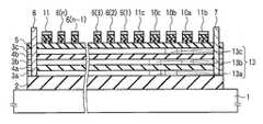
さらに、図1のA-A線に沿う断面である図2に示すように、各シリコン層3にはレイヤー選択トランジスタ10が常時オン(ノーマリーオン)状態になる不純物添加領域がレイヤー選択トランジスタ10のチャネル部の一部領域13に施されている。Further, as shown in FIG. 2 which is a cross section taken along the line AA in FIG. 1, each
例えば、図2で示すように、シリコン層3aでは、レイヤー選択トランジスタ10aのチャネル領域13aに、シリコン層3bではレイヤー選択トランジスタ10bのチャネル領域13bに、シリコン層3cではレイヤー選択トランジスタ10cのチャネル領域13cに、それぞれ不純物添加が施されている。For example, as shown in FIG. 2, in the
尚、不純物の材料としては、N型半導体となる不純物、例えば、砒素(As)リン(P)などの5価元素、また、P型半導体となる不純物、例えば、ホウ素(B)インジウム(In)などの3価元素であり、それらの材料を組み合わせたものでも可能である。As the material of the impurity, an impurity that becomes an N-type semiconductor, for example, a pentavalent element such as arsenic (As) phosphorus (P), or an impurity that becomes a P-type semiconductor, for example, boron (B) indium (In) It is also possible to use a combination of these materials.
各シリコン層3(メモリストリング)は、オン/オフが可能なレイヤー選択トランジスタ10、例えば、チャネルに不純物添加が施されていないレイヤー選択トランジスタ10で制御されることになる。但し、オン/オフ制御可能なレイヤー選択トランジスタ10のチャネルに閾値制御のための不純物添加を行ってもよい。Each silicon layer 3 (memory string) is controlled by a
この場合、シリコン層3aは、レイヤー選択トランジスタ10b、10cで、シリコン層3bは、レイヤー選択トランジスタ10a、10cで、シリコン層3cは、レイヤー選択トランジスタ10a、10bで、それぞれのメモリストリングが制御される。In this case, the
この構造となることで、従来、メモリストリングスのレイヤーそれぞれに独立に形成していたコンタクトを取るための電極は、例えば、図1に代表されるように、電極7及び電極8として、全てのシリコン層3に共通にコンタクトが取れるそれぞれ1つのみを形成すれば良い。With this structure, the electrodes for making contacts that are conventionally formed independently on each memory string layer are all silicon as
従って、メモリストリングを積層させたとしても、メモリストリングの長さの増大は、一層ごとにレイヤー選択トランジスタ10を形成する領域のみとなるため、メモリストリングを積層させるごとにコンタクト用電極と選択トランジスタを形成していた従来の構造に比べてその長さを短くすることが可能となる。Therefore, even if the memory strings are stacked, the increase in the length of the memory string is only in the region where the
尚、電極7、8としては、タングステン(W)の他、アルミニウム(Al)等の金属材料が挙げられる。In addition, as the
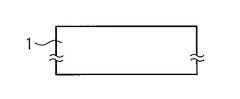
また、集積度を上げるためには、図3に示すように、それぞれのメモリストリングスを並べて配置するのが有効であるが、この場合、従来のようにメモリストリング一層増加ごとにコンタクト電極の数が増加すると、それぞれから引き出される配線数及びその制御のための回路面積が増大してしまう。In order to increase the degree of integration, it is effective to arrange the memory strings side by side as shown in FIG. 3, but in this case, the number of contact electrodes increases as the number of memory strings increases as in the conventional case. If it increases, the number of wires drawn from each of them and the circuit area for controlling them will increase.
一方、本発明では、メモリストリング一層増加ごとにコンタクト用電極の数が増えることは無いため、一層増加ごとにレイヤー選択トランジスタ10が一本増加するのに対応する増大量に抑えることが可能となりチップ面積の縮小が可能となる。On the other hand, in the present invention, since the number of contact electrodes does not increase with each increase in the memory string, it is possible to suppress the increase corresponding to the increase of one
尚、図3では、例として、メモリストリングスが3つ配置した構造を示しているが、これに限定されるものではない。In addition, in FIG. 3, although the structure where three memory strings are arrange | positioned is shown as an example, it is not limited to this.
また、各メモリストリングが制御できる構造であれば、図2に示した形態に限らず適宜変形することが可能である。Further, as long as each memory string can be controlled, the structure is not limited to that shown in FIG. 2, and can be modified as appropriate.
例えば、図8に示すように、複数の不純物添加領域13が、シリコン層3に存在しても良いし、図11に示すように、積層膜6(X)を挟むように両側に形成されていても良い。また、図11に示すように、レイヤー選択トランジスタ10の数は、シリコン層3の数と同じある必要は無く、各メモリストリングが制御できる構成であれば、その数が多くても少なくても良い。For example, as shown in FIG. 8, a plurality of impurity-added
図11のように、レイヤー選択トランジスタを、メモリストリングスを挟み込むように配置すれば、不純物添加領域13の拡散による影響を最小限に抑えることができる。As shown in FIG. 11, if the layer selection transistor is arranged so as to sandwich the memory string, the influence of the diffusion of the impurity-added
但し、メモリストリングスの長さを考えると数が少ない方が短くでき、その分集積度が高まるため望ましい。However, considering the length of the memory strings, the smaller number is preferable because it can be shortened and the degree of integration increases accordingly.
図4A乃至図4Fに、本発明の一実施形態に係る不揮発性半導体記憶装置9の製造工程、特に、シリコン層3における不純物添加領域13の一形成工程を示す。4A to 4F show a manufacturing process of the nonvolatile semiconductor memory device 9 according to an embodiment of the present invention, in particular, a process of forming the impurity added
まず、図4Aに示すように、例えば、面方位(100)、比抵抗10~20Ωcmのp型(第1導電型)シリコン基板1を用意し、このシリコン基板1の上に、シリコン酸化膜層2を介して、シリコン層3aを例えば堆積により積層させる。First, as shown in FIG. 4A, for example, a p-type (first conductivity type)
次に、図では省略するが、フォトエッチングプロセス(Photo Etching Process、以下「PEP」という。いわゆるフォトレジストを使ったリソグラフィ工程)により塗布したレジストに開口を設けるパターニングを行い、イオンインプラ(Ion Implantation)を施すことでシリコン層3a内に不純物添加領域13aを形成する。Next, although not shown in the figure, patterning is performed to provide openings in the resist applied by a photo etching process (Photo Etching Process, hereinafter referred to as “PEP”, a so-called photolithographic lithography process), and ion implantation is performed. As a result, an impurity added
次に、同様の方法で、シリコン酸化膜層4aを介して、シリコン層3bを積層させPEPによるパターニングとイオンインプラを施すことで不純物添加領域13bを形成する。Next, by the same method, the
次に、同様の方法で、シリコン酸化膜層4bを介して、シリコン層3cを積層させPEPによるパターニングとイオンインプラを施すことで不純物添加領域13cを形成する。Next, by the same method, the
次に、シリコン層3cの上に、シリコン酸化膜層5を積層させる。この状態を図4Bに示す。Next, the silicon
次に、シリコン基板1上のシリコン酸化膜層2、シリコン層3a、シリコン酸化膜層4a、シリコン層3b、シリコン酸化膜層4b、シリコン層3c、絶縁膜5を、例えば、PEPによるパターニングの後、異方性ドライエッチングを施すことにより、図4Cで示すような短冊(フィン)形状に加工する。Next, after patterning the silicon
次に、フィン形状に加工したシリコン基板1上のシリコン酸化膜層2、シリコン層3a、シリコン酸化膜層4a、シリコン層3b、シリコン酸化膜層4b、シリコン層3c、絶縁膜5に対して、例えば、熱酸化を施すことによりシリコン酸化膜106aを形成する。Next, with respect to the silicon
このシリコン酸化膜106aは、堆積によっても形成が可能である。また、シリコン酸化膜に限らず、各世代の不揮発性半導体記憶装置で必要なトンネル絶縁膜材料を適宜選択して用いることができる。The
次に、電荷蓄積層106b、絶縁膜106c、電極106dを堆積する。この状態を図4Dに示す。Next, a
次に、図4Eに示すように、シリコン酸化膜106a、電荷蓄積層106b、絶縁膜106c、電極106dを例えば、PEPによるパターニングの後、異方性ドライエッチングを施すことにより、図1で示した、そのそれぞれが電気的に絶縁された積層膜6(X)、レイヤー選択トランジスタ10及び選択トランジスタ11を形成する。Next, as shown in FIG. 4E, the
この時、レイヤー選択トランジスタ10は、それぞれに対応する不純物添加領域13がチャネルとなる位置に形成される必要がある。At this time, the
次に、図では省略するが、例えば、シリコン酸化膜を全体に埋め込み化学機械的研磨(CMP)処理することで、積層膜6(X)、レイヤー選択トランジスタ10、選択トランジスタ11、フィン形状に加工したシリコン基板1上のシリコン酸化膜層2、シリコン層3a、シリコン酸化膜層4a、シリコン層3b、シリコン酸化膜層4b、シリコン層3c、絶縁膜5のそれぞれの間を埋めるような層間絶縁膜を形成する。Next, although not shown in the drawing, for example, a silicon oxide film is entirely embedded and subjected to chemical mechanical polishing (CMP), thereby processing the laminated film 6 (X), the
次に、図4Fに示すように、例えば、PEPによるパターニングの後、異方性ドライエッチングを施すことにより電極7及び電極8を形成する領域にホールパターンを形成する。その後、例えばタングステンの堆積後、ホールパターン以外のタングステンをCMP処理することで電極7及び電極8が形成され、図1の不揮発性半導体記憶装置9が形成される。Next, as shown in FIG. 4F, for example, after patterning by PEP, anisotropic dry etching is performed to form a hole pattern in a region where the
以上は、図1及び図2で示した実施形態を形成する製造工程である。特に図示しないが、他の実施形態もその一部を変更することで形成することが可能である。The above is the manufacturing process for forming the embodiment shown in FIGS. Although not particularly illustrated, other embodiments can be formed by changing a part thereof.
図8で示した構造を形成する場合には、図4A及び図4Bで示す不純物添加領域13を形成する工程において、図8中に示した不純物添加領域13が形成されるようにPEPによるパターニングを変更させれば良い。In the case of forming the structure shown in FIG. 8, in the step of forming the impurity added
図11で示した構造を形成する場合には、図4A及び図4Bで示す不純物添加領域13を形成する工程において、図11中に示した不純物添加領域13が形成されるようにPEPによるパターニングを変更し、さらに、図4Cで示すフィン形状の加工においては、そのフィンの長さがレイヤー選択トランジスタを増加させた分、長くなるようPEPによるパターニングを変更して加工し、その後、図4Eで示す加工でも同様に、図11の構造となるようにPEPによるパターニングを変更して加工すれば良い。When the structure shown in FIG. 11 is formed, in the step of forming the impurity added
このように、各不純物添加領域を形成するにはPEPが必要となるが、コンタクト加工のPEPに比べてラフなPEPで済み、生産コストを抑えることが出来ると同時に、複雑な形状に加工する必要が無く形成がしやすい。また、電極7及び電極8は、加工深さが等しくても良いため、両者は、同時に形成することが可能となる。以上の点で従来よりも有効な構造である。As described above, PEP is required to form each impurity-added region, but rough PEP is sufficient as compared with PEP for contact processing, and it is possible to reduce production costs and to process into a complicated shape. Easy to form. Moreover, since the processing depths of the
図5A乃至図5Cに、本発明の一実施形態に係る不揮発性半導体記憶装置9の製造工程、特に、シリコン層3における不純物添加領域13の一形成工程を示す。5A to 5C show a manufacturing process of the nonvolatile semiconductor memory device 9 according to an embodiment of the present invention, particularly, a process of forming the impurity added
まず、例えば、面方位(100)、比抵抗10~20Ωcmのp型(第1導電型)シリコン基板1を用意し、このシリコン基板1の上に、シリコン酸化膜層2を介して、シリコン層3a、シリコン酸化膜層4a、シリコン層3b、シリコン酸化膜層4b、シリコン層3cと交互に、例えば、堆積により積層させていき、この最表面のシリコン層3の上に絶縁膜5を、例えば、堆積により形成する。この状態を図5Aに示す。First, for example, a p-type (first conductivity type)
次に、PEPによりレジストパターニングを行い、イオンインプラを施すことで、シリコン層3a内に不純物添加領域13aを形成する。この状態を図5Bに示す。Next, resist patterning is performed by PEP, and ion implantation is performed to form an impurity added
次に、同様に、PEPによるパターニングとイオンインプラによりシリコン層3b内に不純物添加領域13bを、シリコン層3c内に不純物添加領域13cを、それぞれ形成する。この時、不純物添加領域13a、13b、13cは、打ち込むイオンのエネルギーを変化させることにより深さを変化させて形成する。この状態を図5Cに示す。Next, similarly, an impurity added
この状態は、前述した図4Bに対応している。この後は図示しないが、図4C~図4Fの図を用いて前述したプロセスと同様な手順で形成することで、図1の不揮発性半導体記憶装置9が形成される。This state corresponds to FIG. 4B described above. Thereafter, although not shown, the non-volatile semiconductor memory device 9 of FIG. 1 is formed by forming in the same procedure as the process described above with reference to FIGS. 4C to 4F.
以上は、図1及び図2で示した実施形態を形成する製造工程である。特に図示しないが、他の実施形態もその一部を変更することで形成することが可能である。The above is the manufacturing process for forming the embodiment shown in FIGS. Although not particularly illustrated, other embodiments can be formed by changing a part thereof.
図8で示した構造を形成する場合には、図5B及び図5Cで示す不純物添加領域13を形成する工程において、図8中に示した不純物添加領域13が形成されるようにPEPによるパターニングを変更させれば良い。When the structure shown in FIG. 8 is formed, patterning by PEP is performed so that the impurity added
図11で示した構造を形成する場合には、図5B及び図5Cで示す不純物添加領域13を形成する工程において、図11中に示した不純物添加領域13が形成されるようにPEPによるパターニングを変更し、さらに、図4Cで示すフィン形状の加工においては、そのフィンの長さがレイヤー選択トランジスタを増加させた分、長くなるようPEPによるパターニングを変更して加工し、その後、図4Eで示す加工でも同様に、図11の構造となるようにPEPによるパターニングを変更して加工すれば良い。In the case of forming the structure shown in FIG. 11, in the step of forming the impurity added
このような形成方法により、シリコン層3を連続的に形成することができ、また、レジストがシリコン層3と接することが無いので、シリコン層3が汚染されることは無く、それによるチャネルとしての特性劣化を抑制することができる。By such a forming method, the
但し、図4A~図4Fで示したプロセスに比べ、不純物添加領域を制御良く形成させるのが難しく、例えば、図5Bにおいて、シリコン層3a内に不純物添加領域13aを形成した際、シリコン層3b、3cにおける不純物添加領域13aの直上の領域内に不純物が添加されてしまう可能性がある。However, compared to the process shown in FIGS. 4A to 4F, it is difficult to form the impurity doped region with good control. For example, when the impurity doped
図6A乃至図6Cに、本発明の一実施形態に係る不揮発性半導体記憶装置9の製造工程、特に、シリコン層3における不純物添加領域13の一形成工程を示す。6A to 6C show a manufacturing process of the nonvolatile semiconductor memory device 9 according to one embodiment of the present invention, in particular, a process of forming the impurity added
まず、図6Aに示すように、例えば、面方位(100)、比抵抗10~20Ωcmのp型(第1導電型)シリコン基板1を用意し、このシリコン基板1の上に、シリコン酸化膜層2を介して、シリコン層3a、シリコン酸化膜層4a、シリコン層3b、シリコン酸化膜層4b、シリコン層3cと交互に、例えば、堆積により積層させていき、この最表面のシリコン層3の上に絶縁膜5を、例えば、堆積により形成する。First, as shown in FIG. 6A, for example, a p-type (first conductivity type)
次に、シリコン基板1上のシリコン酸化膜層2、シリコン層3a、シリコン酸化膜層4a、シリコン層3b、シリコン酸化膜層4b、シリコン層3c、絶縁膜5を、例えば、PEPによるパターニングの後、異方性ドライエッチングを施すことにより、図6Aで示すようなフィン形状に加工する。Next, after patterning the silicon
次に、シリコン酸化膜を堆積し、例えば、PEPによるパターニングの後、異方性ドライエッチングを施すことにより、図6B中、15で示すように、階段形状を有し、かつ、フィン形状に加工された積層膜(シリコン基板1上のシリコン酸化膜層2、シリコン層3a、シリコン酸化膜層4a、シリコン層3b、シリコン酸化膜層4b、シリコン層3c、絶縁膜5)に接するような形状に加工する。Next, a silicon oxide film is deposited and subjected to anisotropic dry etching after patterning by, for example, PEP, so that it has a step shape and is processed into a fin shape as indicated by 15 in FIG. 6B. In such a shape as to come into contact with the laminated film (silicon
この時、階段形状のそれぞれの高さは、シリコン層3a、3b、3cの上端よりも下に位置するのが望ましい。At this time, the height of each of the staircase shapes is preferably located below the upper ends of the
次に、不純物添加領域13を作成するのに望ましい不純物が添加されたシリコン酸化膜を堆積し、例えば、PEPによるパターニングの後、異方性ドライエッチングを施すことにより、図6C中、16で示すように、シリコン酸化膜15の階段形状のそれぞれの上に形成されるような形状に加工する。Next, a silicon oxide film to which an impurity added for forming the impurity-added
この時、16の高さは、それぞれが接しているシリコン層3の上に形成されているシリコン酸化膜4a、4b、絶縁膜5の上端よりも下に位置するのが望ましい。At this time, the height of 16 is preferably located below the upper ends of the
ここで、例えば1000℃の熱を加えることで、不純物添加シリコン酸化膜16から不純物添加シリコン酸化膜16がそれぞれ接しているシリコン層3へと不純物が固層拡散し、不純物添加領域13が形成される。Here, for example, by applying heat at 1000 ° C., impurities are solid-diffused from the impurity-added
次に、シリコン酸化膜15及び不純物添加シリコン酸化膜16を例えば異方性ドライエッチングを施すことにより除去すると、図4Cと同様の構造になる。Next, when the
この後は図示しないが、図4D~図4Fの図を用いて前述したプロセスと同様な手順で形成することで、図1及び図2で示した不揮発性半導体記憶装置9が形成される。After this, although not shown, the nonvolatile semiconductor memory device 9 shown in FIGS. 1 and 2 is formed by forming in the same procedure as the process described above with reference to FIGS. 4D to 4F.
図8で示した構造を形成する場合には、図9で示すように、シリコン酸化膜15及び不純物添加シリコン酸化膜16を入れ替えることで形成が可能となる。8 can be formed by replacing the
まず、シリコン基板1上に、シリコン酸化膜層2、シリコン層3a、シリコン酸化膜層4a、シリコン層3b、シリコン酸化膜層4b、シリコン層3c、絶縁膜5をそれぞれ積層し、例えば、PEPによるパターニングの後、異方性ドライエッチングを施すことによりフィン形状に加工する。First, a silicon
次に、不純物添加シリコン酸化膜を堆積し、例えば、PEPによるパターニングの後、異方性ドライエッチングを施すことにより、図9A中、16aで示すように、階段形状を有し、かつ、フィン形状に加工された積層膜(シリコン基板1上のシリコン酸化膜層2、シリコン層3a、シリコン酸化膜層4a、シリコン層3b、シリコン酸化膜層4b、シリコン層3c、絶縁膜5)に接するような形状に加工する。Next, an impurity-added silicon oxide film is deposited and subjected to anisotropic dry etching after patterning by, for example, PEP, thereby having a step shape and a fin shape as shown by 16a in FIG. 9A. In contact with the laminated film (silicon
この時、階段形状のそれぞれの高さは、シリコン層3a、3b、3cの上端よりも下に位置するのが望ましい。At this time, the height of each of the staircase shapes is preferably located below the upper ends of the
次に、シリコン酸化膜を堆積し、例えば、PEPによるパターニングの後、異方性ドライエッチングを施すことにより、図9B中、15で示すように、不純物添加シリコン酸化膜16aの階段形状のそれぞれの上に形成されるような形状に加工する。Next, a silicon oxide film is deposited and subjected to anisotropic dry etching after patterning by, for example, PEP, so that each of the stepped shapes of the impurity-added
この時、15の高さは、それぞれが接しているシリコン層3の上に形成されているシリコン酸化膜4a、4b、絶縁膜5の上端よりも下に位置するのが望ましい。At this time, the height of 15 is preferably located below the upper ends of the
次に、不純物添加シリコン酸化膜を堆積し、例えば、PEPによるパターニングの後、異方性ドライエッチングを施すことにより、図9C中、16bで示すように、シリコン酸化膜15のそれぞれの上に形成されるような形状に加工する。Next, an impurity-added silicon oxide film is deposited and formed on each of the
ここで、例えば、1000℃の熱を加えることで、不純物添加シリコン酸化膜16a、16bから不純物添加シリコン酸化膜16a、16bがそれぞれ接しているシリコン層3へと不純物が固層拡散し、不純物添加領域13が形成される。Here, for example, by applying heat at 1000 ° C., impurities are solid-diffused from the doped
次に、シリコン酸化膜15及び不純物添加シリコン酸化膜16a、16bを、例えば、異方性ドライエッチングを施すことにより除去すると、図9Dと同様の構造になる。Next, when the
この後は図示しないが、図4D~図4Fの図を用いて前述したプロセスと同様な手順で形成することで、図1及び図8で示した不揮発性半導体記憶装置9が形成される。Thereafter, although not shown, the nonvolatile semiconductor memory device 9 shown in FIGS. 1 and 8 is formed by forming in the same procedure as the process described above with reference to FIGS. 4D to 4F.
特に図示しないが、他の実施形態もその一部を変更することで形成することが可能である。Although not specifically shown, other embodiments can be formed by changing a part thereof.
図7A及び図7Bは、図6A乃至図6Cとその一部が異なる不揮発性半導体記憶装置9の製造工程である。7A and 7B show a manufacturing process of the nonvolatile semiconductor memory device 9 which is partly different from FIGS. 6A to 6C.
まず、シリコン基板1上に、シリコン酸化膜層2、シリコン層3a、シリコン酸化膜層4a、シリコン層3b、シリコン酸化膜層4b、シリコン層3c、絶縁膜5をそれぞれ積層し、例えば、PEPによるパターニングの後、異方性ドライエッチングを施すことによりフィン形状に加工する。First, a silicon
次に、シリコン酸化膜を堆積し、例えば、PEPによるパターニングの後、異方性ドライエッチングを施すことにより、図7A中、15で示すように、階段形状を有し、かつ、フィン形状に加工された積層膜(シリコン基板1上のシリコン酸化膜層2、シリコン層3a、シリコン酸化膜層4a、シリコン層3b、シリコン酸化膜層4b、シリコン層3c、絶縁膜5)に接するような形状に加工する。Next, a silicon oxide film is deposited and, for example, patterned by PEP, and then subjected to anisotropic dry etching so that it has a step shape and is processed into a fin shape as indicated by 15 in FIG. 7A. In such a shape as to come into contact with the laminated film (silicon
この時、階段形状のそれぞれの高さは、シリコン層3a、3b、3cの上端よりも下に位置するのが望ましい。At this time, the height of each of the staircase shapes is preferably located below the upper ends of the
ここで、シリコン絶縁膜層15を図7Aで示すような形状にすることにより、図7Bで示すように、その後の不純物添加シリコン酸化膜層16を形成する際、堆積のみで形成することが可能であり、PEPなどのプロセスを省略できるため、製造コストを低減することができる。Here, by forming the silicon insulating
図7Bの構造に形成した後、例えば、1000℃の熱を加えることで、不純物添加シリコン酸化膜16から不純物添加シリコン酸化膜16がそれぞれ接しているシリコン層3へと不純物が固層拡散し、不純物添加領域13が形成される。After forming the structure of FIG. 7B, for example, by applying heat at 1000 ° C., impurities are solid-diffused from the doped
次に、シリコン酸化膜15及び不純物添加シリコン酸化膜16を例えば異方性ドライエッチングを施すことにより除去すると、図4Cと同様の構造になる。Next, when the
この後は図示しないが、図4D~図4Fの図を用いて前述したプロセスと同様な手順で形成することで、図1及び図2で示した不揮発性半導体記憶装置9が形成される。After this, although not shown, the nonvolatile semiconductor memory device 9 shown in FIGS. 1 and 2 is formed by forming in the same procedure as the process described above with reference to FIGS. 4D to 4F.
図10A及び図10Bは、図9A乃至図9Dとその一部が異なる不揮発性半導体記憶装置9の製造工程である。10A and 10B show a manufacturing process of the nonvolatile semiconductor memory device 9 which is partly different from FIGS. 9A to 9D.
まず、シリコン基板1上に、シリコン酸化膜層2、シリコン層3a、シリコン酸化膜層4a、シリコン層3b、シリコン酸化膜層4b、シリコン層3c、絶縁膜5をそれぞれ積層し、例えば、PEPによるパターニングの後、異方性ドライエッチングを施すことによりフィン形状に加工する。First, a silicon
次に、不純物添加シリコン酸化膜を堆積し、例えば、PEPによるパターニングの後、異方性ドライエッチングを施すことにより、図10A中、16aで示すように、階段形状を有し、かつ、フィン形状に加工された積層膜(シリコン基板1上のシリコン酸化膜層2、シリコン層3a、シリコン酸化膜層4a、シリコン層3b、シリコン酸化膜層4b、シリコン層3c、絶縁膜5)に接するような形状に加工する。Next, an impurity-added silicon oxide film is deposited and subjected to anisotropic dry etching after patterning by, for example, PEP, thereby having a step shape and a fin shape as shown by 16a in FIG. 10A. In contact with the laminated film (silicon
この時、階段形状のそれぞれの高さは、シリコン層3a、3b、3cの上端よりも下に位置するのが望ましい。At this time, the height of each of the staircase shapes is preferably located below the upper ends of the
次に、シリコン酸化膜を堆積し、例えば、PEPによるパターニングの後、異方性ドライエッチングを施すことにより、図10A中、15で示すように、不純物添加シリコン酸化膜16aの階段形状のそれぞれの上及びそれ以外の積層フィン構造を覆うような形状に加工する。Next, by depositing a silicon oxide film and performing, for example, anisotropic dry etching after patterning by PEP, as shown by 15 in FIG. 10A, each of the stepped shapes of the doped
この時、不純物添加シリコン酸化膜層16a上に形成された15の高さは、それぞれが接しているシリコン層3の上に形成されているシリコン酸化膜4a、4b、絶縁膜5の上端よりも下に位置するのが望ましい。At this time, the
ここで、シリコン絶縁膜層15を図10Aで示すような形状にすることにより、図10Bで示すようにその後の不純物添加シリコン酸化膜層16bを形成する際、堆積のみで形成することが可能であり、PEPなどのプロセスを省略できるため、製造コストを低減することができる。Here, by forming the silicon insulating
図10Bの構造に形成した後、例えば、1000℃の熱を加えることで、不純物添加シリコン酸化膜16a、16bから不純物添加シリコン酸化膜16a、16bがそれぞれ接しているシリコン層3へと不純物が固層拡散し、不純物添加領域13が形成される。After forming the structure of FIG. 10B, for example, by applying heat at 1000 ° C., impurities are solidified from the doped
次に、シリコン酸化膜15及び不純物添加シリコン酸化膜16a,16bを、例えば、異方性ドライエッチングを施すことにより除去すると、図9Dと同様の構造になる。Next, when the
この後は図示しないが、図4D~図4Fの図を用いて前述したプロセスと同様な手順で形成することで、図1及び図8で示した不揮発性半導体記憶装置9が形成される。Thereafter, although not shown, the nonvolatile semiconductor memory device 9 shown in FIGS. 1 and 8 is formed by forming in the same procedure as the process described above with reference to FIGS. 4D to 4F.
図10Aの構造からは、図10Bの構造を形成しなくても図9Dと同様の構造が形成できる。From the structure of FIG. 10A, a structure similar to FIG. 9D can be formed without forming the structure of FIG. 10B.
まず、図10Aの構造に形成した後、不純物添加領域13を作成するのに望ましい不純物を含むガス雰囲気中で熱処理を加えると、シリコン酸化膜15及び不純物添加シリコン酸化膜16aで覆われていないシリコン層3中に不純物が拡散し、また、一方で、不純物添加シリコン酸化膜16aから不純物添加シリコン酸化膜16aが接しているシリコン層3へと不純物が固層拡散することになり不純物添加領域13が形成される。First, after the formation of the structure of FIG. 10A, when heat treatment is performed in a gas atmosphere containing impurities desirable for forming the impurity-added
特に図示しないが、他の実施形態もその一部を変更することで形成することが可能である。Although not specifically shown, other embodiments can be formed by changing a part thereof.
図6A乃至図6C、図7A及び図7B、図9A乃至図9D、図10A及び図10Bで示した方法で形成する場合、不純物添加領域13の位置関係は、不純物添加シリコン酸化膜16、16a、16bのそれぞれの形状で決まるため、図4A乃至図4F、図5A乃至図5Cで示した方法で形成した場合において、イオンインプラのためのPEPによるパターニングを行う際、それぞれの領域の位置関係がPEPの精度により保たれなくなってしまうという問題を回避できる。When formed by the method shown in FIGS. 6A to 6C, 7A and 7B, 9A to 9D, 10A and 10B, the positional relationship of the impurity-added
但し、シリコン酸化膜15及び不純物添加シリコン酸化膜16、16a、16bを階段状に加工する際に高さ制御が必要な形状の加工が必要となり、層が増加するとさらに困難度が上がってしまう。However, when the
また、図6A乃至図6C、図7A及び図7B、図9A乃至図9D、図10A及び図10Bでは、フィン形状の両側を挟み込むように、シリコン酸化膜15及び不純物添加シリコン酸化膜16、16a16bを形成していたが、片側にのみ形成した場合でも可能である。但し、気相拡散を用いる場合は、もう一方の片側を全てシリコン層3への意図しない固相拡散が起こらない任意の層で覆う必要がある。6A to 6C, FIGS. 7A and 7B, FIGS. 9A to 9D, and FIGS. 10A and 10B, the
また、図6A乃至図6C、図7A及び図7B、図9A乃至図9D、図10A及び図10Bでは、シリコン酸化膜を用いたが、材料はこれに限らず不純物を固層拡散させることができる材料であれば特に制限しない。6A to 6C, FIGS. 7A and 7B, FIGS. 9A to 9D, and FIGS. 10A and 10B use a silicon oxide film, but the material is not limited to this, and impurities can be diffused into a solid layer. If it is material, there will be no restriction | limiting in particular.
図12A及び図12Bは、本発明の一実施形態に係る不揮発性半導体記憶装置の断面図である。12A and 12B are cross-sectional views of the nonvolatile semiconductor memory device according to the embodiment of the present invention.
図12Aは、図8で示した構造に、さらに、選択トランジスタ11bを追加した構造である。FIG. 12A shows a structure in which a
このような構造をとることでメモリストリングスのカットオフ特性が向上し、誤動作を抑制することができる。その場合、図12Bに示すように選択トランジスタ11cをさらに追加することでその効果は得られる。Such a structure improves the cut-off characteristics of the memory string and can suppress malfunction. In that case, the effect can be obtained by further adding a
但し、選択トランジスタを増やした分、メモリストリングスの長さが長くなり、集積度を高めるという観点からは、選択トランジスタを増加しすぎることは望ましくない。However, it is not desirable to increase the number of select transistors from the viewpoint of increasing the integration degree by increasing the length of the memory string by increasing the number of select transistors.
図13は、本発明の一実施形態に係る不揮発性半導体記憶装置の断面図である。FIG. 13 is a cross-sectional view of a nonvolatile semiconductor memory device according to an embodiment of the present invention.
図2に示した構造と異なるのは、シリコン層3はそれぞれの不純物添加領域13で途切れており、また、各シリコン層3のそれぞれの上に積層された絶縁膜4a、4b、5は、各シリコン層3における不純物添加領域13のそれぞれの直上から途切れており、途切れた先の領域は、シリコン層14となっていることである。2 is different from the structure shown in FIG. 2 in that the
即ち、各シリコン層3は、不純物添加領域13を介して、各シリコン層3とは異なる別のシリコン層14により互いに接続される。That is, the silicon layers 3 are connected to each other by another
この構造となることで、レイヤー選択トランジスタのチャネル部分のストリングが太くなり、その分電気抵抗が低くなるため、図2の構造よりもレイヤー選択が高速化し、メモリセルを高速に動作させることができる。By adopting this structure, the string of the channel portion of the layer selection transistor becomes thicker and the electrical resistance is correspondingly reduced. Therefore, the layer selection is faster than the structure of FIG. 2, and the memory cell can be operated at high speed. .
この例では、不純物添加領域13は、シリコン層3cでは、メモリストリングスに最も近いレイヤー選択トランジスタのチャネルに設けられ、そのレイヤー選択トランジスタを制御不可能状態にする。In this example, the
また、不純物添加領域13は、シリコン層3bでは、メモリストリングスにから2番目に近いレイヤー選択トランジスタのチャネルに設けられ、そのレイヤー選択トランジスタを制御不可能状態にする。Further, in the
さらに、不純物添加領域13は、シリコン層3aでは、メモリストリングスから最も遠いレイヤー選択トランジスタのチャネルに設けられ、そのレイヤー選択トランジスタを制御不可能状態にする。Further, the impurity added
但し、この順番は、これに限られることはなく、逆であってもよい。However, this order is not limited to this and may be reversed.
図14A乃至図14Eは、本発明の一実施形態に係る不揮発性半導体記憶装置の製造工程である。14A to 14E show a manufacturing process of the nonvolatile semiconductor memory device according to the embodiment of the present invention.
まず、例えば、面方位(100)、比抵抗10~20Ωcmのp型(第1導電型)シリコン基板1を用意し、このシリコン基板1の上に、シリコン酸化膜層2を介して、シリコン層3a、シリコン酸化膜層4a、シリコン層3b、シリコン酸化膜層4b、シリコン層3cと交互に、例えば、堆積により積層させていき、この最表面のシリコン層3の上に絶縁膜5を、例えば、堆積により形成する。First, for example, a p-type (first conductivity type)
次に、シリコン基板1上のシリコン酸化膜層2、シリコン層3a、シリコン酸化膜層4a、シリコン層3b、シリコン酸化膜層4b、シリコン層3c、絶縁膜5からなる積層膜の一部を、図14Aで示すように、シリコン層3がそれぞれ一部露出するような階段形状に、例えば、PEPによるパターニングの後、異方性ドライエッチングを施すことにより加工する。Next, a part of the laminated film composed of the silicon
次に、イオンインプラにより、シリコン層3の露出部に不純物添加領域13を形成する。この状態を図14Bに示す。この時必要あれば、不純物添加領域13のみを開口するPEPによるパターニングを行っても良い。Next, an impurity added
次に、図14Cに示すように、シリコンを堆積し、例えばCMPで平坦化処理を行うことでシリコン層14を形成する。シリコン層14の平坦化は、ドライエッチングでも形成可能である。Next, as shown in FIG. 14C, silicon is deposited, and a
また、この時、シリコンを不純物添加領域13の上にエピタキシャル成長させて単結晶状態に形成しても良い。シリコン層が多結晶状態だと、結晶粒界を電流が流れてしまい、レイヤー選択トランジスタ10のオフ特性が劣化してしまうため、シリコン層14は、単結晶状態が望ましい。また、シリコン層14の上に絶縁膜を形成し、シリコン層14を保護しても良い。At this time, silicon may be epitaxially grown on the impurity-added
次に、例えば、PEPによるパターニングの後、異方性ドライエッチングを施すことにより、図14Cに示した積層構造を、図14Dで示すようなフィン形状に加工する。Next, for example, by performing anisotropic dry etching after patterning by PEP, the laminated structure shown in FIG. 14C is processed into a fin shape as shown in FIG. 14D.
詳しい説明は省略するが、その後、図4D~図4Fの図を用いて前述したプロセスと同様な手順で形成することで、図14Eで示す構造となり、図13で示す不揮発性半導体記憶装置9が形成される。Although a detailed description is omitted, the structure shown in FIG. 14E is obtained by forming in the same procedure as described above with reference to FIGS. 4D to 4F, and the nonvolatile semiconductor memory device 9 shown in FIG. It is formed.
図15は、本発明の一実施形態に係る不揮発性半導体記憶装置の断面図である。FIG. 15 is a cross-sectional view of a nonvolatile semiconductor memory device according to an embodiment of the present invention.
図2に示した構造と異なるのは、メモリストリングへのコンタクト用電極7の周りに、不純物添加シリコン17が形成されている。2 is different from the structure shown in FIG. 2 in that an impurity-added
本実施形態において、例えば、電極7がビット線に接続されているとし、電極8がソース線に接続されているとし、シリコン層3内の不純物添加領域13及び不純物添加シリコン17がそれぞれn+型となっている場合における書き込みと消去の動作例を以下に示す。In this embodiment, for example, it is assumed that the
本実施形態は、本発明を限定するものではない。以下の実施形態において、p型半導体の構成要素をn型半導体に代え、かつ、n型半導体の構成要素をp型半導体に代えてもよい。This embodiment does not limit the present invention. In the following embodiments, the constituent element of the p-type semiconductor may be replaced with an n-type semiconductor, and the constituent element of the n-type semiconductor may be replaced with a p-type semiconductor.
書き込みは、ソース線コンタクト電極8とビット線コンタクト電極7とを接地し、選択トランジスタ11にはバイアスを印加せず、レイヤー選択トランジスタ10a、10b及び各メモリセル6(X=1~n)の制御ゲート6(X=1~n)dに正のバイアスを印加することで、メモリストリングスのチャネルとなるシリコン層3a、3b、3cにn型の蓄積領域を生じさせる。For writing, the source
次いで、書き込みたいメモリセル、例えば、メモリセル6(3)の制御ゲート6(3)dに大きな正のバイアスを印加しメモリセル6(3)の電荷蓄積層6(3)bに電子を注入し書き込みを行う。Next, a large positive bias is applied to the memory cell to be written, for example, the control gate 6 (3) d of the memory cell 6 (3) to inject electrons into the charge storage layer 6 (3) b of the memory cell 6 (3). And write.
この時、レイヤー選択トランジスタ10cにはバイアスが印加されていないので、シリコン層3a、3bをチャネルとするメモリセル6(3)には書き込まれず、シリコン層3cをチャネルとするメモリセル6(3)のみが書き込まれる。At this time, since no bias is applied to the
また、書き込みたくないメモリセル、例えば6(3)以外の6(X)の制御ゲート6(X)dについては、負のバイアスを印加しても良い。Further, a negative bias may be applied to a memory cell that is not desired to be written, for example, 6 (X) control gate 6 (X) d other than 6 (3).
消去は、ビット線コンタクト電極7を接地し、選択トランジスタ11、レイヤー選択トランジスタ10a、10b、10c及び各6(X=1~n)の制御ゲート6(X=1~n)dに負のバイアスを印加することで、メモリストリングスのチャネルとなるシリコン層3a、3b、3cにp型の蓄積領域を生じさせる。In erasing, the bit
次いで、消去したいメモリセル、例えば、メモリセル6(2)の制御ゲート6(2)dに大きな負のバイアスを印加して、メモリセル6(2)の電荷蓄積層6(2)bにホールを注入し消去を行う。Next, a large negative bias is applied to the memory cell to be erased, for example, the control gate 6 (2) d of the memory cell 6 (2), and holes are formed in the charge storage layer 6 (2) b of the memory cell 6 (2). Inject and erase.
この時、消去したくないメモリセル、例えば、メモリセル6(2)以外の6(X)の制御ゲート6(X)dに正のバイアスを印加しても良い。At this time, a positive bias may be applied to a memory cell that is not desired to be erased, for example, a control gate 6 (X) d of 6 (X) other than the memory cell 6 (2).
読み出しは、通常のNAND型フラッシュメモリと同様、ソース線コンタクト電極7を接地、ビット線コンタクト電極8に正のバイアスを印加して、読み出したいメモリセル、例えば、メモリセル6(1)以外のメモリセル6(X)の制御ゲート6(X)dに正のバイアスを印加し、電流が流れるか否かで“0”又は“1”の情報として読み出しを行う。In the read operation, the source
この場合も同様に、レイヤー選択ゲート10a、10b、10cのバイアス印加の方法により積層されたメモリストリングを選択し、読み出すことができる。In this case, similarly, the memory strings stacked by the bias application method of the
以上の動作は、ソース線コンタクト電極8とビット線コンタクト電極7の両方に不純物領域17が形成されていない図2の場合も、書き込み及び消去は、本実施形態と同様に行うことができるが、ショットキー障壁によるソース抵抗が、読み出し時に流れる電流を著しく小さくする可能性がある。ちなみに、このようなショットキー障壁は、ドレイン領域側では問題になることはないため、本実施形態では上述の問題は生じない。In the case of FIG. 2 in which the
また、本実施形態は、電極8が金属材料で形成されており、電極7が不純物添加シリコンにより形成されていても同様の効果が得られる、その場合、電極7の周りに、不純物添加シリコン17が形成されていなくても良い。In the present embodiment, the same effect can be obtained even if the
図16A及び図16Bは、本発明の一実施形態に係る不揮発性半導体記憶装置9における、特に、積層膜6により囲まれたシリコン層3の概略構成図である。16A and 16B are schematic configuration diagrams of the
各シリコン層3a、3b、3cは、積層膜6で囲まれた部分において、それぞれエアーギャップ18a、18b、18cを有する。このエアーギャップ18a、18b、18cは、絶縁膜4a,4b,5に形成される。The silicon layers 3a, 3b, and 3c have
エアーギャップ18a、18b、18cは、積層膜6に囲まれた部分だけではなく、レイヤー選択トランジスタ10、選択トランジスタ11で囲まれた部分に形成されていても良いし、さらには、シリコン層3a,3b,3cの間の全体に広がっていても良い。The
その場合、シリコン層3a,3b,3c間の比誘電率が低くなり、その間を狭くしても同じ絶縁特性が得られる。その結果、シリコン層3a,3b,3c間を狭めることができ、集積度を高めることができる。In that case, the relative dielectric constant between the
図18A乃至図18Hは、本発明の一実施形態に係る不揮発性半導体記憶装置の製造工程、特に、シリコン層3おけるエアーギャップを含む絶縁層18の一形成工程を示す。18A to 18H show a manufacturing process of the nonvolatile semiconductor memory device according to one embodiment of the present invention, in particular, a forming process of the insulating
これらの図は、図1のB-B線に沿う断面に相当する。These figures correspond to a cross section taken along line BB in FIG.
まず、図18Aに示すように、例えば、面方位(100)、比抵抗10~20Ωcmのp型(第1導電型)シリコン基板1を用意し、このシリコン基板1の上に、シリコンゲルマニウム(SiGe)層102を介して、シリコン層3とシリコンゲルマニウム層104とが3a、104a、3b、104b、3cとなるように交互に積層する。First, as shown in FIG. 18A, for example, a p-type (first conductivity type)
この時、シリコンとシリコンゲルマニウムは、シリコン基板1と結晶学的方位関係を保ちつつ結晶膜を堆積成長するエピタキシャル成長をさせることができるため、シリコン層3とシリコンゲルマニウム層104は単結晶で形成することができる。この最表面のシリコン層3の上に絶縁膜5を例えば堆積により形成する。この状態を図18Bに示す。At this time, since silicon and silicon germanium can be epitaxially grown by depositing and growing a crystal film while maintaining a crystallographic orientation relationship with the
次に、シリコン基板1上のシリコンゲルマニウム層102、シリコン層3a、シリコンゲルマニウム層104a、シリコン層3b、シリコンゲルマニウム層104b、シリコン層3c、絶縁膜5からなる積層構造を、例えば、PEPによるパターニングの後、異方性ドライエッチングを施すことにより、図18Cで示すような短冊形状に加工する。Next, a stacked structure including the
次に、図18Dに示すように、短冊形状に加工したシリコンゲルマニウム層102、シリコン層3a、シリコンゲルマニウム層104a、シリコン層3b、シリコンゲルマニウム層104b、シリコン層3c、絶縁膜5に対して、例えば、熱酸化を施すことによりシリコン酸化膜106aを形成する。Next, as shown in FIG. 18D, for the
この時、シリコンゲルマニウム層102、104上にはシリコンゲルマニウム酸化膜が形成される。このシリコン酸化膜106aは堆積によっても形成が可能である。また、シリコン酸化膜に限らず、各世代の不揮発性半導体記憶装置で必要なトンネル絶縁膜材料を適宜選択して用いることができる。At this time, a silicon germanium oxide film is formed on the silicon germanium layers 102 and 104. This
次に、図18Eに示すように、電荷蓄積層106b、絶縁膜106c、電極106dを堆積する。Next, as shown in FIG. 18E, a
次に、図18Fに示すように、シリコン酸化膜106a、電荷蓄積層106b、絶縁膜106c、電極106dを例えば、PEPによるパターニングの後、異方性ドライエッチングを施すことにより、図1で示した、そのそれぞれが電気的に絶縁された積層膜6(X)を形成する。Next, as shown in FIG. 18F, the
次に、図18Gに示すように、例えば等方性エッチングによりシリコンゲルマニウム層102、104のみを選択的に除去する。Next, as shown in FIG. 18G, only the silicon germanium layers 102 and 104 are selectively removed by isotropic etching, for example.
ここで、図18Fにおいて、シリコンゲルマニウム層102、104は、積層膜6(X)により全て囲まれているように示しているが、実際には、積層膜6(X)のそれぞれの間には空隙があり、その空隙からシリコンゲルマニウム層102、104はエッチングされる。Here, in FIG. 18F, the silicon germanium layers 102 and 104 are shown to be surrounded by the laminated film 6 (X), but actually, between the laminated films 6 (X), There is a void, and the silicon germanium layers 102 and 104 are etched from the void.
次いで、図18Hに示すように、例えば、シリコン酸化膜を全体に堆積させ、シリコンゲルマニウム層102、104が除去された領域に、シリコン酸化膜2及びシリコン酸化膜4を形成する。ここで、シリコン酸化膜2及びシリコン酸化膜4はその領域がすべてシリコン酸化膜で形成される必要はなく。その一部、又は全くシリコン酸化膜が形成されないエアーギャップの状態でも良い。Next, as shown in FIG. 18H, for example, a silicon oxide film is deposited on the entire surface, and the
また、その際、例えば埋め込み性能の悪いシリコン酸化膜を堆積させることで、積層膜6(X)、レイヤー選択トランジスタ10及び選択トランジスタ11で囲まれた空隙は、優先的に埋め込みが起こらず、エアーギャップを含んだ絶縁層18a、18b、18cが形成される。At this time, for example, by depositing a silicon oxide film having poor embedding performance, the space surrounded by the laminated film 6 (X), the
この後は図示しないが、例えば、PEPによるパターニングの後、異方性ドライエッチングを施すことにより電極7及び電極8を形成する領域にホールパターンを形成する。Thereafter, although not shown, for example, after patterning by PEP, anisotropic dry etching is performed to form a hole pattern in a region where the
その後、例えば、タングステンの堆積後、ホールパターン以外のタングステンをCMP処理することで電極7及び電極8が形成され、図16A及び図16Bで示したエアーギャップを含んだ絶縁層18を備えた不揮発性半導体記憶装置9が形成される。After that, for example, after depositing tungsten, the
図17は、本発明の一実施形態に係る不揮発性半導体記憶装置9の概略構成図である。FIG. 17 is a schematic configuration diagram of the nonvolatile semiconductor memory device 9 according to one embodiment of the present invention.
シリコン基板1上のシリコン酸化膜層2、シリコン層3a、シリコン酸化膜層4a、シリコン層3b、シリコン酸化膜層4b、シリコン層3c、絶縁膜5の積層構造からなる2本のフィン構造の間に消去用電極19が形成されており、積層膜6(X)からなるメモリセルの消去動作時にはこの消去用電極19にバイアスを印加することによってメモリセルの電荷蓄積層6(X)bにホールを注入し、動作させることができる構造である。Between two fin structures composed of a laminated structure of a silicon
この時、図16A及び図16Bで示したエアーギャップを含んだ絶縁層18が備わることで、消去用電極19にバイアスを印加した際、消去用電極19から絶縁層18方向へのフリンジ電界が弱まり、それぞれのシリコン層3への電界が集中する結果、消去特性を向上させることができる。At this time, since the insulating
(変形例)
尚、本発明は、上述した各実施形態に限定されるものではなく、本発明の要旨を逸脱しない範囲で、各実施形態の一部を適宜組み合わせて実施することができる。(Modification)
In addition, this invention is not limited to each embodiment mentioned above, In the range which does not deviate from the summary of this invention, it can implement by combining a part of each embodiment suitably.
また、実施形態の形成方法も限定されるわけではなく、例えば、Si単結晶でチャネルを形成する目的で図18に示したSiGeとSiのエピタキシャル成長による形成方法を用いても良い。Also, the formation method of the embodiment is not limited, and for example, the formation method by epitaxial growth of SiGe and Si shown in FIG. 18 may be used for the purpose of forming a channel with Si single crystal.
Si単結晶でチャネルを形成させることでセル電流値を稼ぐことが可能となり、さらに、単結晶シリコン上に熱酸化プロセスによるトンネル膜を形成することができるため、不揮発性半導体記憶装置としての書き込み、保持特性などの特性向上が期待される。By forming a channel with Si single crystal, it becomes possible to earn a cell current value, and furthermore, since a tunnel film by a thermal oxidation process can be formed on single crystal silicon, writing as a nonvolatile semiconductor memory device, Expected to improve characteristics such as retention characteristics.
また、実施形態では基板としてシリコンを用いたが、ゲルマニウム基板など他の基板を用いることも可能である。In the embodiment, silicon is used as the substrate, but other substrates such as a germanium substrate can also be used.
また、シリコン層3における積層膜6(X)からなるメモリセル、選択トランジスタ11、レイヤー選択トランジスタ10a、10b、10cそれぞれの間の拡散層領域については説明していないが、適宜必要な拡散層を形成すれば良い。Further, the diffusion layer region between each of the memory cell composed of the laminated film 6 (X) in the
また、例えば電極6(X)dに電圧を印加すると積層膜6(X)直下だけではなく積層膜6(X)間のシリコン層3にも電界(フリンジ電界)がかかり、ゲート間隔(積層膜6(X)間隔)が短く、例えば30nm以下となる場合には、そのフリンジ電界だけでもチャネルに電流パスが通るため(例えば、Chang-Hyum Lee, et al, VLSI Technology Digest of Technical Papers, pp118-119, 2008)、拡散層が形成されていなくても良い。For example, when a voltage is applied to the electrode 6 (X) d, an electric field (fringe electric field) is applied not only directly below the laminated film 6 (X) but also to the
その他、本発明の要旨を逸脱しない範囲で、種々変形して実施することができる。Other various modifications can be made without departing from the scope of the present invention.
(効果)
本発明によれば、レイヤー選択トランジスタ構造により、ソース線及びビット線が積層ストリングでそれぞれ共通の一本ずつとなり、メモリストリングを積層させたとしても長さの増大は一層ごとにレイヤー選択トランジスタを形成する領域のみとなるため、従来の構造に比べてその長さを短くすることが可能となる。また、配線数及び回路面積も同様に一層ごとにレイヤー選択トランジスタ一本が増加するのに対応する増大量に抑えることが可能となる。(effect)
According to the present invention, due to the layer selection transistor structure, the source line and the bit line are common to each of the stacked strings, and even if the memory strings are stacked, the increase in length forms a layer selection transistor for each layer. Therefore, the length can be shortened as compared with the conventional structure. Similarly, the number of wirings and the circuit area can be suppressed to an increase corresponding to the increase of one layer selection transistor for each layer.
本発明は、高速ランダム書き込み可能なファイルメモリ、高速ダウンロード可能な携帯端末、高速ダウンロード可能な携帯プレーヤー、放送機器用半導体メモリ、ドライブレコーダ、ホームビデオ、通信用大容量バッファメモリ、防犯カメラ用半導体メモリなどに対して産業上のメリットは多大である。The present invention relates to a file memory capable of high-speed random writing, a portable terminal capable of high-speed download, a portable player capable of high-speed download, a semiconductor memory for broadcasting equipment, a drive recorder, a home video, a large-capacity buffer memory for communication, and a semiconductor memory for security camera The industrial merit is great.
1…シリコン(Si)基板(半導体基板)、2…シリコン酸化膜(SiO2)、3(3a、3b、3c)…シリコン層(メモリストリングチャネル領域)、4(4a、4b)…シリコン酸化膜(メモリストリング絶縁領域)、5…シリコン酸化膜、6(X)…積層膜(Xは1~nの自然数)、6(X)a…シリコン酸化膜(メモリセルトンネル絶縁膜)、6(X)b…シリコン窒化膜(Si3N4)(メモリセル電荷蓄積層)、6(X)c…シリコン酸化膜(メモリセルブロック絶縁膜)、6(X)d…ニッケルシリサイド(NiSi)(メモリセルコントロール電極)、7、…タングステン(W)(メモリストリング独立コンタクト)、8…タングステン(メモリストリング共通コンタクト)、9…不揮発性半導体記憶装置、10(10a、10b、10c)…レイヤー選択トランジスタ、11、11b、11c…選択トランジスタ、13(13a、13b、13c)…シリコン層3における不純物添加領域、14…シリコン層、15…シリコン酸化膜、16、16a、16b…不純物添加シリコン酸化膜、17…不純物添加シリコン(拡散層領域)、18(18a、18b、18c)…エアーギャップを含む絶縁層、19…消去用電極、102…シリコンゲルマニウム(SiGe)層、104(104a、104b)…シリコンゲルマニウム層、106a…シリコン酸化膜、106b…シリコン窒化膜、106c…シリコン酸化膜、106d…ニッケルシリサイド。DESCRIPTION OF
Claims (10)
Translated fromJapanese前記第1乃至第nのメモリストリングスは、前記第1方向に互いに絶縁されて積み重ねられる第1乃至第nの半導体層と、前記第1乃至第nの半導体層の前記第1及び第2方向に垂直な第3方向の側面上に、第1の絶縁膜、電荷蓄積層、第2の絶縁膜及びコントロールゲート電極の順番で、前記第3方向に積み重ねられる第1の積層構造とを有し、
前記第1乃至第nのメモリストリングスは、前記第1乃至第nの半導体層をチャネルとし、前記第2方向に直列に接続される電気的に書き換え可能な第1乃至第mのメモリセル(mは2以上の自然数)を有し、
前記コントロールゲート電極は、前記第1乃至第nの半導体層に跨って形成され、
前記第1乃至第kのレイヤー選択トランジスタは、前記第1乃至第nの半導体層の前記第3方向の側面上に、第3の絶縁膜及び第1のセレクトゲート電極の順番で、前記第3方向に積み重ねられる第2の積層構造を有し、
前記第1乃至第kのレイヤー選択トランジスタは、前記第1乃至第nの半導体層をチャネルとし、前記第1乃至第mのメモリセルに対して前記第2方向に直列に接続され、
前記第1のセレクトゲート電極は、前記第1乃至第nの半導体層に跨って形成され、
前記第1乃至第kのレイヤー選択トランジスタの各々は、前記第1乃至第nの半導体層のうちの少なくとも1つで常時オンの制御不可能状態であり、残りの少なくとも1つの半導体層でオン/オフが可能である制御可能状態であり、
前記第1乃至第kのレイヤー選択トランジスタの前記第1乃至第nの半導体層での前記制御不可能状態/前記制御可能状態の関係は、互いに異なっている
ことを特徴とする不揮発性半導体記憶装置。First to nth memory strings (n is a natural number of 2 or more) stacked in a first direction perpendicular to the surface of the semiconductor substrate and extending in a second direction parallel to the surface of the semiconductor substrate. And first to k-th layer selection transistors (k is a natural number of 2 or more) for selecting one of the first to n-th memory strings,
The first to nth memory strings are insulated from each other in the first direction and stacked in a first direction to an nth semiconductor layer, and the first to nth semiconductor layers in the first and second directions. A first laminated structure stacked in the third direction in the order of a first insulating film, a charge storage layer, a second insulating film, and a control gate electrode on a side surface in a vertical third direction;
The first to nth memory strings are electrically rewritable first to mth memory cells (m) connected in series in the second direction with the first to nth semiconductor layers as channels. Is a natural number of 2 or more)
The control gate electrode is formed across the first to nth semiconductor layers,
The first to kth layer selection transistors are arranged on the side surfaces in the third direction of the first to nth semiconductor layers in the order of a third insulating film and a first select gate electrode. Having a second laminated structure stacked in a direction,
The first to kth layer selection transistors are connected in series in the second direction with respect to the first to mth memory cells, with the first to nth semiconductor layers as channels.
The first select gate electrode is formed across the first to nth semiconductor layers,
Each of the first to kth layer selection transistors is always in an uncontrollable state in at least one of the first to nth semiconductor layers, and is turned on / off in the remaining at least one semiconductor layer. A controllable state that can be turned off,
The non-controllable state / controllable state relationship of the first to kth layer selection transistors in the first to nth semiconductor layers is different from each other. .
前記追加の選択トランジスタは、前記第1乃至第nの半導体層の前記第3方向の側面上に、第4の絶縁膜及び第2のセレクトゲート電極の順番で、前記第3方向に積み重ねられる第3の積層構造を有し、
前記第2のセレクトゲート電極は、前記第1乃至第nの半導体層に跨って形成され、
前記追加の選択トランジスタは、前記第1乃至第nの半導体層の全てで前記制御可能状態である
ことを特徴とする請求項1に記載の不揮発性半導体記憶装置。An additional selection transistor connected in series in the second direction with respect to the first to kth layer selection transistors using the first to nth semiconductor layers as a channel;
The additional selection transistors are stacked in the third direction on the side surfaces in the third direction of the first to nth semiconductor layers in the order of the fourth insulating film and the second select gate electrode. 3 laminated structure,
The second select gate electrode is formed across the first to nth semiconductor layers,
The nonvolatile semiconductor memory device according to claim 1, wherein the additional selection transistor is in the controllable state in all of the first to nth semiconductor layers.
前記第1乃至第kのレイヤー選択トランジスタのうち前記第1乃至第nのメモリストリングスに最も近いレイヤー選択トランジスタは、前記第1乃至第nの半導体層のうち最上層の半導体層で前記制御不可能状態であり、
前記第1乃至第kのレイヤー選択トランジスタのうち前記第1乃至第nのメモリストリングスにi番目(iは、2~n-1のうちの1つ)に近いレイヤー選択トランジスタは、前記第1乃至第nの半導体層のうち最上層からi番目の半導体層で前記制御不可能状態であり、
前記第1乃至第kのレイヤー選択トランジスタのうち前記第1乃至第nのメモリストリングスから最も遠いレイヤー選択トランジスタは、前記第1乃至第nの半導体層のうち最下層の半導体層で前記制御不可能状態であり、
前記制御不可能状態は、前記第1乃至第nの半導体層内に形成される不純物領域により実現し、前記第1乃至第nの半導体層は、前記不純物領域を介して前記第1乃至第nの半導体層とは別の半導体層により互いに結合されている
ことを特徴とする請求項1に記載の不揮発性半導体記憶装置。K is equal to n;
Of the first to k-th layer selection transistors, the layer selection transistor closest to the first to n-th memory strings is not controllable in the uppermost semiconductor layer of the first to n-th semiconductor layers. State
Among the first to kth layer selection transistors, the i-th (i is one of 2 to n−1) closest layer selection transistors to the first to nth memory strings are the first to kth layer selection transistors. The i-th semiconductor layer from the uppermost layer among the n-th semiconductor layers is in the uncontrollable state,
Of the first to kth layer selection transistors, the layer selection transistor farthest from the first to nth memory strings is not controllable in the lowest semiconductor layer of the first to nth semiconductor layers. State
The uncontrollable state is realized by impurity regions formed in the first to n-th semiconductor layers, and the first to n-th semiconductor layers pass through the impurity regions and the first to n-th semiconductor layers. The nonvolatile semiconductor memory device according to claim 1, wherein the semiconductor layers are coupled to each other by a semiconductor layer different from the semiconductor layer.
前記追加の選択トランジスタは、前記第1乃至第nの半導体層の前記第3方向の側面上に、第4の絶縁膜及び第2のセレクトゲート電極の順番で、前記第3方向に積み重ねられる第3の積層構造を有し、
前記第2のセレクトゲート電極は、前記第1乃至第nの半導体層に跨って形成され、
前記追加の選択トランジスタは、前記第1乃至第nの半導体層の全てで前記制御可能状態である
ことを特徴とする請求項3に記載の不揮発性半導体記憶装置。An additional selection transistor connected in series in the second direction with respect to the first to nth layer selection transistors using the first to nth semiconductor layers as a channel;
The additional selection transistors are stacked in the third direction on the side surfaces in the third direction of the first to nth semiconductor layers in the order of the fourth insulating film and the second select gate electrode. 3 laminated structure,
The second select gate electrode is formed across the first to nth semiconductor layers,
The nonvolatile semiconductor memory device according to claim 3, wherein the additional selection transistor is in the controllable state in all of the first to nth semiconductor layers.
Priority Applications (3)
| Application Number | Priority Date | Filing Date | Title |
|---|---|---|---|
| JP2011518196AJP5456036B2 (en) | 2009-06-12 | 2009-06-12 | Nonvolatile semiconductor memory device |
| PCT/JP2009/060803WO2010143306A1 (en) | 2009-06-12 | 2009-06-12 | Nonvolatile semiconductor storage device |
| US13/316,603US8779502B2 (en) | 2009-06-12 | 2011-12-12 | Nonvolatile semiconductor memory |
Applications Claiming Priority (1)
| Application Number | Priority Date | Filing Date | Title |
|---|---|---|---|
| PCT/JP2009/060803WO2010143306A1 (en) | 2009-06-12 | 2009-06-12 | Nonvolatile semiconductor storage device |
Related Child Applications (1)
| Application Number | Title | Priority Date | Filing Date |
|---|---|---|---|
| US13/316,603ContinuationUS8779502B2 (en) | 2009-06-12 | 2011-12-12 | Nonvolatile semiconductor memory |
Publications (1)
| Publication Number | Publication Date |
|---|---|
| WO2010143306A1true WO2010143306A1 (en) | 2010-12-16 |
Family
ID=43308574
Family Applications (1)
| Application Number | Title | Priority Date | Filing Date |
|---|---|---|---|
| PCT/JP2009/060803CeasedWO2010143306A1 (en) | 2009-06-12 | 2009-06-12 | Nonvolatile semiconductor storage device |
Country Status (3)
| Country | Link |
|---|---|
| US (1) | US8779502B2 (en) |
| JP (1) | JP5456036B2 (en) |
| WO (1) | WO2010143306A1 (en) |
Cited By (11)
| Publication number | Priority date | Publication date | Assignee | Title |
|---|---|---|---|---|
| JP2012234885A (en)* | 2011-04-28 | 2012-11-29 | Toshiba Corp | Semiconductor device and manufacturing method of the same |
| US8435857B2 (en) | 2011-01-17 | 2013-05-07 | Kabushiki Kaisha Toshiba | Method for manufacturing semiconductor memory device |
| JP2013115260A (en)* | 2011-11-29 | 2013-06-10 | Toshiba Corp | Semiconductor device and manufacturing method of the same |
| JP2013143536A (en)* | 2012-01-12 | 2013-07-22 | Toshiba Corp | Semiconductor device and method of manufacturing the same |
| US8569829B2 (en) | 2009-12-28 | 2013-10-29 | Kabushiki Kaisha Toshiba | Nonvolatile semiconductor memory device |
| WO2015033417A1 (en)* | 2013-09-05 | 2015-03-12 | 株式会社 東芝 | Semiconductor storage device and data writing method |
| WO2015037159A1 (en)* | 2013-09-13 | 2015-03-19 | 株式会社 東芝 | Semiconductor memory device and memory system |
| JP2016015193A (en)* | 2012-01-30 | 2016-01-28 | 群聯電子股▲ふん▼有限公司 | Operation method for nand flash memory unit |
| US9305936B2 (en) | 2013-07-03 | 2016-04-05 | Kabushiki Kaisha Toshiba | Nonvolatile semiconductor memory device and method of manufacturing the same |
| US9564450B2 (en) | 2010-09-21 | 2017-02-07 | Kabushiki Kaisha Toshiba | Nonvolatile semiconductor memory device and method of manufacturing the same |
| US9768380B2 (en) | 2011-07-15 | 2017-09-19 | Kabushiki Kaisha Toshiba | Nonvolatile semiconductor memory device and method of manufacturing the same |
Families Citing this family (361)
| Publication number | Priority date | Publication date | Assignee | Title |
|---|---|---|---|---|
| US10378106B2 (en) | 2008-11-14 | 2019-08-13 | Asm Ip Holding B.V. | Method of forming insulation film by modified PEALD |
| US9394608B2 (en) | 2009-04-06 | 2016-07-19 | Asm America, Inc. | Semiconductor processing reactor and components thereof |
| US8802201B2 (en) | 2009-08-14 | 2014-08-12 | Asm America, Inc. | Systems and methods for thin-film deposition of metal oxides using excited nitrogen-oxygen species |
| WO2011114502A1 (en)* | 2010-03-19 | 2011-09-22 | 株式会社 東芝 | Nonvolatile semiconductor storage device and method for producing same |
| WO2011114503A1 (en) | 2010-03-19 | 2011-09-22 | 株式会社 東芝 | Nonvolatile semiconductor storage device and method for producing same |
| US9312155B2 (en) | 2011-06-06 | 2016-04-12 | Asm Japan K.K. | High-throughput semiconductor-processing apparatus equipped with multiple dual-chamber modules |
| US10364496B2 (en) | 2011-06-27 | 2019-07-30 | Asm Ip Holding B.V. | Dual section module having shared and unshared mass flow controllers |
| US10854498B2 (en) | 2011-07-15 | 2020-12-01 | Asm Ip Holding B.V. | Wafer-supporting device and method for producing same |
| US20130023129A1 (en) | 2011-07-20 | 2013-01-24 | Asm America, Inc. | Pressure transmitter for a semiconductor processing environment |
| US9017481B1 (en) | 2011-10-28 | 2015-04-28 | Asm America, Inc. | Process feed management for semiconductor substrate processing |
| US20140048867A1 (en)* | 2012-08-20 | 2014-02-20 | Globalfoundries Singapore Pte. Ltd. | Multi-time programmable memory |
| US9659799B2 (en) | 2012-08-28 | 2017-05-23 | Asm Ip Holding B.V. | Systems and methods for dynamic semiconductor process scheduling |
| US10714315B2 (en) | 2012-10-12 | 2020-07-14 | Asm Ip Holdings B.V. | Semiconductor reaction chamber showerhead |
| US20160376700A1 (en) | 2013-02-01 | 2016-12-29 | Asm Ip Holding B.V. | System for treatment of deposition reactor |
| US9484191B2 (en) | 2013-03-08 | 2016-11-01 | Asm Ip Holding B.V. | Pulsed remote plasma method and system |
| US9589770B2 (en) | 2013-03-08 | 2017-03-07 | Asm Ip Holding B.V. | Method and systems for in-situ formation of intermediate reactive species |
| JP2014179530A (en)* | 2013-03-15 | 2014-09-25 | Toshiba Corp | Method for manufacturing non-volatile semiconductor memory device |
| US9240412B2 (en) | 2013-09-27 | 2016-01-19 | Asm Ip Holding B.V. | Semiconductor structure and device and methods of forming same using selective epitaxial process |
| US10683571B2 (en) | 2014-02-25 | 2020-06-16 | Asm Ip Holding B.V. | Gas supply manifold and method of supplying gases to chamber using same |
| JP2015167200A (en) | 2014-03-04 | 2015-09-24 | 株式会社東芝 | Non-volatile semiconductor storage device |
| US10167557B2 (en) | 2014-03-18 | 2019-01-01 | Asm Ip Holding B.V. | Gas distribution system, reactor including the system, and methods of using the same |
| US11015245B2 (en) | 2014-03-19 | 2021-05-25 | Asm Ip Holding B.V. | Gas-phase reactor and system having exhaust plenum and components thereof |
| KR101536530B1 (en)* | 2014-07-15 | 2015-07-15 | 한양대학교 산학협력단 | Fin field effect transistor |
| US10858737B2 (en) | 2014-07-28 | 2020-12-08 | Asm Ip Holding B.V. | Showerhead assembly and components thereof |
| US9890456B2 (en) | 2014-08-21 | 2018-02-13 | Asm Ip Holding B.V. | Method and system for in situ formation of gas-phase compounds |
| US9252153B1 (en)* | 2014-09-22 | 2016-02-02 | Macronix International Co., Ltd. | Method of word-line formation by semi-damascene process with thin protective conductor layer |
| US9657845B2 (en) | 2014-10-07 | 2017-05-23 | Asm Ip Holding B.V. | Variable conductance gas distribution apparatus and method |
| US10941490B2 (en) | 2014-10-07 | 2021-03-09 | Asm Ip Holding B.V. | Multiple temperature range susceptor, assembly, reactor and system including the susceptor, and methods of using the same |
| KR102263121B1 (en) | 2014-12-22 | 2021-06-09 | 에이에스엠 아이피 홀딩 비.브이. | Semiconductor device and manufacuring method thereof |
| US10529542B2 (en) | 2015-03-11 | 2020-01-07 | Asm Ip Holdings B.V. | Cross-flow reactor and method |
| US10276355B2 (en) | 2015-03-12 | 2019-04-30 | Asm Ip Holding B.V. | Multi-zone reactor, system including the reactor, and method of using the same |
| US10458018B2 (en) | 2015-06-26 | 2019-10-29 | Asm Ip Holding B.V. | Structures including metal carbide material, devices including the structures, and methods of forming same |
| US10600673B2 (en) | 2015-07-07 | 2020-03-24 | Asm Ip Holding B.V. | Magnetic susceptor to baseplate seal |
| JP2017054941A (en)* | 2015-09-10 | 2017-03-16 | 株式会社東芝 | Semiconductor device and method of manufacturing the same |
| US9960072B2 (en) | 2015-09-29 | 2018-05-01 | Asm Ip Holding B.V. | Variable adjustment for precise matching of multiple chamber cavity housings |
| US10211308B2 (en) | 2015-10-21 | 2019-02-19 | Asm Ip Holding B.V. | NbMC layers |
| US10322384B2 (en) | 2015-11-09 | 2019-06-18 | Asm Ip Holding B.V. | Counter flow mixer for process chamber |
| US11139308B2 (en) | 2015-12-29 | 2021-10-05 | Asm Ip Holding B.V. | Atomic layer deposition of III-V compounds to form V-NAND devices |
| US10468251B2 (en) | 2016-02-19 | 2019-11-05 | Asm Ip Holding B.V. | Method for forming spacers using silicon nitride film for spacer-defined multiple patterning |
| US10529554B2 (en) | 2016-02-19 | 2020-01-07 | Asm Ip Holding B.V. | Method for forming silicon nitride film selectively on sidewalls or flat surfaces of trenches |
| US10501866B2 (en) | 2016-03-09 | 2019-12-10 | Asm Ip Holding B.V. | Gas distribution apparatus for improved film uniformity in an epitaxial system |
| US10343920B2 (en) | 2016-03-18 | 2019-07-09 | Asm Ip Holding B.V. | Aligned carbon nanotubes |
| US9892913B2 (en) | 2016-03-24 | 2018-02-13 | Asm Ip Holding B.V. | Radial and thickness control via biased multi-port injection settings |
| US10865475B2 (en) | 2016-04-21 | 2020-12-15 | Asm Ip Holding B.V. | Deposition of metal borides and silicides |
| US10190213B2 (en) | 2016-04-21 | 2019-01-29 | Asm Ip Holding B.V. | Deposition of metal borides |
| US10032628B2 (en) | 2016-05-02 | 2018-07-24 | Asm Ip Holding B.V. | Source/drain performance through conformal solid state doping |
| US10367080B2 (en) | 2016-05-02 | 2019-07-30 | Asm Ip Holding B.V. | Method of forming a germanium oxynitride film |
| KR102592471B1 (en) | 2016-05-17 | 2023-10-20 | 에이에스엠 아이피 홀딩 비.브이. | Method of forming metal interconnection and method of fabricating semiconductor device using the same |
| US11453943B2 (en) | 2016-05-25 | 2022-09-27 | Asm Ip Holding B.V. | Method for forming carbon-containing silicon/metal oxide or nitride film by ALD using silicon precursor and hydrocarbon precursor |
| US10388509B2 (en) | 2016-06-28 | 2019-08-20 | Asm Ip Holding B.V. | Formation of epitaxial layers via dislocation filtering |
| US9859151B1 (en) | 2016-07-08 | 2018-01-02 | Asm Ip Holding B.V. | Selective film deposition method to form air gaps |
| US10612137B2 (en) | 2016-07-08 | 2020-04-07 | Asm Ip Holdings B.V. | Organic reactants for atomic layer deposition |
| US10714385B2 (en) | 2016-07-19 | 2020-07-14 | Asm Ip Holding B.V. | Selective deposition of tungsten |
| KR102354490B1 (en) | 2016-07-27 | 2022-01-21 | 에이에스엠 아이피 홀딩 비.브이. | Method of processing a substrate |
| US10395919B2 (en) | 2016-07-28 | 2019-08-27 | Asm Ip Holding B.V. | Method and apparatus for filling a gap |
| US9812320B1 (en) | 2016-07-28 | 2017-11-07 | Asm Ip Holding B.V. | Method and apparatus for filling a gap |
| KR102532607B1 (en) | 2016-07-28 | 2023-05-15 | 에이에스엠 아이피 홀딩 비.브이. | Substrate processing apparatus and method of operating the same |
| US9887082B1 (en) | 2016-07-28 | 2018-02-06 | Asm Ip Holding B.V. | Method and apparatus for filling a gap |
| US9589970B1 (en)* | 2016-08-02 | 2017-03-07 | United Microelectronics Corp. | Antifuse one-time programmable memory |
| KR102613349B1 (en) | 2016-08-25 | 2023-12-14 | 에이에스엠 아이피 홀딩 비.브이. | Exhaust apparatus and substrate processing apparatus and thin film fabricating method using the same |
| US10090316B2 (en)* | 2016-09-01 | 2018-10-02 | Asm Ip Holding B.V. | 3D stacked multilayer semiconductor memory using doped select transistor channel |
| US10410943B2 (en) | 2016-10-13 | 2019-09-10 | Asm Ip Holding B.V. | Method for passivating a surface of a semiconductor and related systems |
| US10643826B2 (en) | 2016-10-26 | 2020-05-05 | Asm Ip Holdings B.V. | Methods for thermally calibrating reaction chambers |
| US11532757B2 (en) | 2016-10-27 | 2022-12-20 | Asm Ip Holding B.V. | Deposition of charge trapping layers |
| US10643904B2 (en) | 2016-11-01 | 2020-05-05 | Asm Ip Holdings B.V. | Methods for forming a semiconductor device and related semiconductor device structures |
| US10229833B2 (en) | 2016-11-01 | 2019-03-12 | Asm Ip Holding B.V. | Methods for forming a transition metal nitride film on a substrate by atomic layer deposition and related semiconductor device structures |
| US10435790B2 (en) | 2016-11-01 | 2019-10-08 | Asm Ip Holding B.V. | Method of subatmospheric plasma-enhanced ALD using capacitively coupled electrodes with narrow gap |
| US10714350B2 (en) | 2016-11-01 | 2020-07-14 | ASM IP Holdings, B.V. | Methods for forming a transition metal niobium nitride film on a substrate by atomic layer deposition and related semiconductor device structures |
| US10134757B2 (en) | 2016-11-07 | 2018-11-20 | Asm Ip Holding B.V. | Method of processing a substrate and a device manufactured by using the method |
| KR102546317B1 (en) | 2016-11-15 | 2023-06-21 | 에이에스엠 아이피 홀딩 비.브이. | Gas supply unit and substrate processing apparatus including the same |
| US10340135B2 (en) | 2016-11-28 | 2019-07-02 | Asm Ip Holding B.V. | Method of topologically restricted plasma-enhanced cyclic deposition of silicon or metal nitride |
| KR102762543B1 (en) | 2016-12-14 | 2025-02-05 | 에이에스엠 아이피 홀딩 비.브이. | Substrate processing apparatus |
| US11447861B2 (en) | 2016-12-15 | 2022-09-20 | Asm Ip Holding B.V. | Sequential infiltration synthesis apparatus and a method of forming a patterned structure |
| US11581186B2 (en) | 2016-12-15 | 2023-02-14 | Asm Ip Holding B.V. | Sequential infiltration synthesis apparatus |
| KR102700194B1 (en) | 2016-12-19 | 2024-08-28 | 에이에스엠 아이피 홀딩 비.브이. | Substrate processing apparatus |
| US10269558B2 (en) | 2016-12-22 | 2019-04-23 | Asm Ip Holding B.V. | Method of forming a structure on a substrate |
| US10867788B2 (en) | 2016-12-28 | 2020-12-15 | Asm Ip Holding B.V. | Method of forming a structure on a substrate |
| US11390950B2 (en) | 2017-01-10 | 2022-07-19 | Asm Ip Holding B.V. | Reactor system and method to reduce residue buildup during a film deposition process |
| US10655221B2 (en) | 2017-02-09 | 2020-05-19 | Asm Ip Holding B.V. | Method for depositing oxide film by thermal ALD and PEALD |
| US10468261B2 (en) | 2017-02-15 | 2019-11-05 | Asm Ip Holding B.V. | Methods for forming a metallic film on a substrate by cyclical deposition and related semiconductor device structures |
| US10283353B2 (en) | 2017-03-29 | 2019-05-07 | Asm Ip Holding B.V. | Method of reforming insulating film deposited on substrate with recess pattern |
| US10529563B2 (en) | 2017-03-29 | 2020-01-07 | Asm Ip Holdings B.V. | Method for forming doped metal oxide films on a substrate by cyclical deposition and related semiconductor device structures |
| KR102457289B1 (en) | 2017-04-25 | 2022-10-21 | 에이에스엠 아이피 홀딩 비.브이. | Method for depositing a thin film and manufacturing a semiconductor device |
| US10770286B2 (en) | 2017-05-08 | 2020-09-08 | Asm Ip Holdings B.V. | Methods for selectively forming a silicon nitride film on a substrate and related semiconductor device structures |
| US10892156B2 (en) | 2017-05-08 | 2021-01-12 | Asm Ip Holding B.V. | Methods for forming a silicon nitride film on a substrate and related semiconductor device structures |
| US10446393B2 (en) | 2017-05-08 | 2019-10-15 | Asm Ip Holding B.V. | Methods for forming silicon-containing epitaxial layers and related semiconductor device structures |
| US10504742B2 (en) | 2017-05-31 | 2019-12-10 | Asm Ip Holding B.V. | Method of atomic layer etching using hydrogen plasma |
| US10886123B2 (en) | 2017-06-02 | 2021-01-05 | Asm Ip Holding B.V. | Methods for forming low temperature semiconductor layers and related semiconductor device structures |
| US12040200B2 (en) | 2017-06-20 | 2024-07-16 | Asm Ip Holding B.V. | Semiconductor processing apparatus and methods for calibrating a semiconductor processing apparatus |
| US11306395B2 (en) | 2017-06-28 | 2022-04-19 | Asm Ip Holding B.V. | Methods for depositing a transition metal nitride film on a substrate by atomic layer deposition and related deposition apparatus |
| US10685834B2 (en) | 2017-07-05 | 2020-06-16 | Asm Ip Holdings B.V. | Methods for forming a silicon germanium tin layer and related semiconductor device structures |
| KR20190009245A (en) | 2017-07-18 | 2019-01-28 | 에이에스엠 아이피 홀딩 비.브이. | Methods for forming a semiconductor device structure and related semiconductor device structures |
| US11374112B2 (en) | 2017-07-19 | 2022-06-28 | Asm Ip Holding B.V. | Method for depositing a group IV semiconductor and related semiconductor device structures |
| US11018002B2 (en) | 2017-07-19 | 2021-05-25 | Asm Ip Holding B.V. | Method for selectively depositing a Group IV semiconductor and related semiconductor device structures |
| US10541333B2 (en) | 2017-07-19 | 2020-01-21 | Asm Ip Holding B.V. | Method for depositing a group IV semiconductor and related semiconductor device structures |
| US10605530B2 (en) | 2017-07-26 | 2020-03-31 | Asm Ip Holding B.V. | Assembly of a liner and a flange for a vertical furnace as well as the liner and the vertical furnace |
| US10312055B2 (en) | 2017-07-26 | 2019-06-04 | Asm Ip Holding B.V. | Method of depositing film by PEALD using negative bias |
| US10590535B2 (en) | 2017-07-26 | 2020-03-17 | Asm Ip Holdings B.V. | Chemical treatment, deposition and/or infiltration apparatus and method for using the same |
| TWI815813B (en) | 2017-08-04 | 2023-09-21 | 荷蘭商Asm智慧財產控股公司 | Showerhead assembly for distributing a gas within a reaction chamber |
| US10770336B2 (en) | 2017-08-08 | 2020-09-08 | Asm Ip Holding B.V. | Substrate lift mechanism and reactor including same |
| US10692741B2 (en) | 2017-08-08 | 2020-06-23 | Asm Ip Holdings B.V. | Radiation shield |
| US11769682B2 (en) | 2017-08-09 | 2023-09-26 | Asm Ip Holding B.V. | Storage apparatus for storing cassettes for substrates and processing apparatus equipped therewith |
| US11139191B2 (en) | 2017-08-09 | 2021-10-05 | Asm Ip Holding B.V. | Storage apparatus for storing cassettes for substrates and processing apparatus equipped therewith |
| US10249524B2 (en) | 2017-08-09 | 2019-04-02 | Asm Ip Holding B.V. | Cassette holder assembly for a substrate cassette and holding member for use in such assembly |
| USD900036S1 (en) | 2017-08-24 | 2020-10-27 | Asm Ip Holding B.V. | Heater electrical connector and adapter |
| US11830730B2 (en) | 2017-08-29 | 2023-11-28 | Asm Ip Holding B.V. | Layer forming method and apparatus |
| US11295980B2 (en) | 2017-08-30 | 2022-04-05 | Asm Ip Holding B.V. | Methods for depositing a molybdenum metal film over a dielectric surface of a substrate by a cyclical deposition process and related semiconductor device structures |
| KR102491945B1 (en) | 2017-08-30 | 2023-01-26 | 에이에스엠 아이피 홀딩 비.브이. | Substrate processing apparatus |
| US11056344B2 (en) | 2017-08-30 | 2021-07-06 | Asm Ip Holding B.V. | Layer forming method |
| KR102401446B1 (en) | 2017-08-31 | 2022-05-24 | 에이에스엠 아이피 홀딩 비.브이. | Substrate processing apparatus |
| US10607895B2 (en) | 2017-09-18 | 2020-03-31 | Asm Ip Holdings B.V. | Method for forming a semiconductor device structure comprising a gate fill metal |
| KR102630301B1 (en) | 2017-09-21 | 2024-01-29 | 에이에스엠 아이피 홀딩 비.브이. | Method of sequential infiltration synthesis treatment of infiltrateable material and structures and devices formed using same |
| US10844484B2 (en) | 2017-09-22 | 2020-11-24 | Asm Ip Holding B.V. | Apparatus for dispensing a vapor phase reactant to a reaction chamber and related methods |
| US10658205B2 (en) | 2017-09-28 | 2020-05-19 | Asm Ip Holdings B.V. | Chemical dispensing apparatus and methods for dispensing a chemical to a reaction chamber |
| US10403504B2 (en) | 2017-10-05 | 2019-09-03 | Asm Ip Holding B.V. | Method for selectively depositing a metallic film on a substrate |
| US10319588B2 (en) | 2017-10-10 | 2019-06-11 | Asm Ip Holding B.V. | Method for depositing a metal chalcogenide on a substrate by cyclical deposition |
| US10923344B2 (en) | 2017-10-30 | 2021-02-16 | Asm Ip Holding B.V. | Methods for forming a semiconductor structure and related semiconductor structures |
| KR102443047B1 (en) | 2017-11-16 | 2022-09-14 | 에이에스엠 아이피 홀딩 비.브이. | Method of processing a substrate and a device manufactured by the same |
| US10910262B2 (en) | 2017-11-16 | 2021-02-02 | Asm Ip Holding B.V. | Method of selectively depositing a capping layer structure on a semiconductor device structure |
| US11022879B2 (en) | 2017-11-24 | 2021-06-01 | Asm Ip Holding B.V. | Method of forming an enhanced unexposed photoresist layer |
| WO2019103613A1 (en) | 2017-11-27 | 2019-05-31 | Asm Ip Holding B.V. | A storage device for storing wafer cassettes for use with a batch furnace |
| CN111344522B (en) | 2017-11-27 | 2022-04-12 | 阿斯莫Ip控股公司 | Including clean mini-environment device |
| US10290508B1 (en) | 2017-12-05 | 2019-05-14 | Asm Ip Holding B.V. | Method for forming vertical spacers for spacer-defined patterning |
| US10872771B2 (en) | 2018-01-16 | 2020-12-22 | Asm Ip Holding B. V. | Method for depositing a material film on a substrate within a reaction chamber by a cyclical deposition process and related device structures |
| KR102695659B1 (en) | 2018-01-19 | 2024-08-14 | 에이에스엠 아이피 홀딩 비.브이. | Method for depositing a gap filling layer by plasma assisted deposition |
| TWI799494B (en) | 2018-01-19 | 2023-04-21 | 荷蘭商Asm 智慧財產控股公司 | Deposition method |
| USD903477S1 (en) | 2018-01-24 | 2020-12-01 | Asm Ip Holdings B.V. | Metal clamp |
| US11018047B2 (en) | 2018-01-25 | 2021-05-25 | Asm Ip Holding B.V. | Hybrid lift pin |
| USD880437S1 (en) | 2018-02-01 | 2020-04-07 | Asm Ip Holding B.V. | Gas supply plate for semiconductor manufacturing apparatus |
| US10535516B2 (en) | 2018-02-01 | 2020-01-14 | Asm Ip Holdings B.V. | Method for depositing a semiconductor structure on a surface of a substrate and related semiconductor structures |
| US11081345B2 (en) | 2018-02-06 | 2021-08-03 | Asm Ip Holding B.V. | Method of post-deposition treatment for silicon oxide film |
| WO2019158960A1 (en) | 2018-02-14 | 2019-08-22 | Asm Ip Holding B.V. | A method for depositing a ruthenium-containing film on a substrate by a cyclical deposition process |
| US10896820B2 (en) | 2018-02-14 | 2021-01-19 | Asm Ip Holding B.V. | Method for depositing a ruthenium-containing film on a substrate by a cyclical deposition process |
| US10731249B2 (en) | 2018-02-15 | 2020-08-04 | Asm Ip Holding B.V. | Method of forming a transition metal containing film on a substrate by a cyclical deposition process, a method for supplying a transition metal halide compound to a reaction chamber, and related vapor deposition apparatus |
| US10658181B2 (en) | 2018-02-20 | 2020-05-19 | Asm Ip Holding B.V. | Method of spacer-defined direct patterning in semiconductor fabrication |
| KR102636427B1 (en) | 2018-02-20 | 2024-02-13 | 에이에스엠 아이피 홀딩 비.브이. | Substrate processing method and apparatus |
| US10975470B2 (en) | 2018-02-23 | 2021-04-13 | Asm Ip Holding B.V. | Apparatus for detecting or monitoring for a chemical precursor in a high temperature environment |
| US11473195B2 (en) | 2018-03-01 | 2022-10-18 | Asm Ip Holding B.V. | Semiconductor processing apparatus and a method for processing a substrate |
| US11629406B2 (en) | 2018-03-09 | 2023-04-18 | Asm Ip Holding B.V. | Semiconductor processing apparatus comprising one or more pyrometers for measuring a temperature of a substrate during transfer of the substrate |
| US11114283B2 (en) | 2018-03-16 | 2021-09-07 | Asm Ip Holding B.V. | Reactor, system including the reactor, and methods of manufacturing and using same |
| KR102646467B1 (en) | 2018-03-27 | 2024-03-11 | 에이에스엠 아이피 홀딩 비.브이. | Method of forming an electrode on a substrate and a semiconductor device structure including an electrode |
| US10510536B2 (en) | 2018-03-29 | 2019-12-17 | Asm Ip Holding B.V. | Method of depositing a co-doped polysilicon film on a surface of a substrate within a reaction chamber |
| US11230766B2 (en) | 2018-03-29 | 2022-01-25 | Asm Ip Holding B.V. | Substrate processing apparatus and method |
| US11088002B2 (en) | 2018-03-29 | 2021-08-10 | Asm Ip Holding B.V. | Substrate rack and a substrate processing system and method |
| KR102501472B1 (en) | 2018-03-30 | 2023-02-20 | 에이에스엠 아이피 홀딩 비.브이. | Substrate processing method |
| KR102600229B1 (en) | 2018-04-09 | 2023-11-10 | 에이에스엠 아이피 홀딩 비.브이. | Substrate supporting device, substrate processing apparatus including the same and substrate processing method |
| TWI811348B (en) | 2018-05-08 | 2023-08-11 | 荷蘭商Asm 智慧財產控股公司 | Methods for depositing an oxide film on a substrate by a cyclical deposition process and related device structures |
| US12025484B2 (en) | 2018-05-08 | 2024-07-02 | Asm Ip Holding B.V. | Thin film forming method |
| US12272527B2 (en) | 2018-05-09 | 2025-04-08 | Asm Ip Holding B.V. | Apparatus for use with hydrogen radicals and method of using same |
| KR20190129718A (en) | 2018-05-11 | 2019-11-20 | 에이에스엠 아이피 홀딩 비.브이. | Methods for forming a doped metal carbide film on a substrate and related semiconductor device structures |
| KR102596988B1 (en) | 2018-05-28 | 2023-10-31 | 에이에스엠 아이피 홀딩 비.브이. | Method of processing a substrate and a device manufactured by the same |
| US11718913B2 (en) | 2018-06-04 | 2023-08-08 | Asm Ip Holding B.V. | Gas distribution system and reactor system including same |
| TWI840362B (en) | 2018-06-04 | 2024-05-01 | 荷蘭商Asm Ip私人控股有限公司 | Wafer handling chamber with moisture reduction |
| US11286562B2 (en) | 2018-06-08 | 2022-03-29 | Asm Ip Holding B.V. | Gas-phase chemical reactor and method of using same |
| KR102568797B1 (en) | 2018-06-21 | 2023-08-21 | 에이에스엠 아이피 홀딩 비.브이. | Substrate processing system |
| US10797133B2 (en) | 2018-06-21 | 2020-10-06 | Asm Ip Holding B.V. | Method for depositing a phosphorus doped silicon arsenide film and related semiconductor device structures |
| KR102854019B1 (en) | 2018-06-27 | 2025-09-02 | 에이에스엠 아이피 홀딩 비.브이. | Periodic deposition method for forming a metal-containing material and films and structures comprising the metal-containing material |
| TWI873894B (en) | 2018-06-27 | 2025-02-21 | 荷蘭商Asm Ip私人控股有限公司 | Cyclic deposition methods for forming metal-containing material and films and structures including the metal-containing material |
| KR102686758B1 (en) | 2018-06-29 | 2024-07-18 | 에이에스엠 아이피 홀딩 비.브이. | Method for depositing a thin film and manufacturing a semiconductor device |
| US10612136B2 (en) | 2018-06-29 | 2020-04-07 | ASM IP Holding, B.V. | Temperature-controlled flange and reactor system including same |
| US10755922B2 (en) | 2018-07-03 | 2020-08-25 | Asm Ip Holding B.V. | Method for depositing silicon-free carbon-containing film as gap-fill layer by pulse plasma-assisted deposition |
| US10388513B1 (en) | 2018-07-03 | 2019-08-20 | Asm Ip Holding B.V. | Method for depositing silicon-free carbon-containing film as gap-fill layer by pulse plasma-assisted deposition |
| US10767789B2 (en) | 2018-07-16 | 2020-09-08 | Asm Ip Holding B.V. | Diaphragm valves, valve components, and methods for forming valve components |
| US10483099B1 (en) | 2018-07-26 | 2019-11-19 | Asm Ip Holding B.V. | Method for forming thermally stable organosilicon polymer film |
| US11053591B2 (en) | 2018-08-06 | 2021-07-06 | Asm Ip Holding B.V. | Multi-port gas injection system and reactor system including same |
| US10883175B2 (en) | 2018-08-09 | 2021-01-05 | Asm Ip Holding B.V. | Vertical furnace for processing substrates and a liner for use therein |
| US10829852B2 (en) | 2018-08-16 | 2020-11-10 | Asm Ip Holding B.V. | Gas distribution device for a wafer processing apparatus |
| US11430674B2 (en) | 2018-08-22 | 2022-08-30 | Asm Ip Holding B.V. | Sensor array, apparatus for dispensing a vapor phase reactant to a reaction chamber and related methods |
| US11024523B2 (en) | 2018-09-11 | 2021-06-01 | Asm Ip Holding B.V. | Substrate processing apparatus and method |
| KR102707956B1 (en) | 2018-09-11 | 2024-09-19 | 에이에스엠 아이피 홀딩 비.브이. | Method for deposition of a thin film |
| US11049751B2 (en) | 2018-09-14 | 2021-06-29 | Asm Ip Holding B.V. | Cassette supply system to store and handle cassettes and processing apparatus equipped therewith |
| CN110970344B (en) | 2018-10-01 | 2024-10-25 | Asmip控股有限公司 | Substrate holding apparatus, system comprising the same and method of using the same |
| US11232963B2 (en) | 2018-10-03 | 2022-01-25 | Asm Ip Holding B.V. | Substrate processing apparatus and method |
| KR102592699B1 (en) | 2018-10-08 | 2023-10-23 | 에이에스엠 아이피 홀딩 비.브이. | Substrate support unit and apparatuses for depositing thin film and processing the substrate including the same |
| US10847365B2 (en) | 2018-10-11 | 2020-11-24 | Asm Ip Holding B.V. | Method of forming conformal silicon carbide film by cyclic CVD |
| US10811256B2 (en) | 2018-10-16 | 2020-10-20 | Asm Ip Holding B.V. | Method for etching a carbon-containing feature |
| KR102605121B1 (en) | 2018-10-19 | 2023-11-23 | 에이에스엠 아이피 홀딩 비.브이. | Substrate processing apparatus and substrate processing method |
| KR102546322B1 (en) | 2018-10-19 | 2023-06-21 | 에이에스엠 아이피 홀딩 비.브이. | Substrate processing apparatus and substrate processing method |
| USD948463S1 (en) | 2018-10-24 | 2022-04-12 | Asm Ip Holding B.V. | Susceptor for semiconductor substrate supporting apparatus |
| US10381219B1 (en) | 2018-10-25 | 2019-08-13 | Asm Ip Holding B.V. | Methods for forming a silicon nitride film |
| US12378665B2 (en) | 2018-10-26 | 2025-08-05 | Asm Ip Holding B.V. | High temperature coatings for a preclean and etch apparatus and related methods |
| US11087997B2 (en) | 2018-10-31 | 2021-08-10 | Asm Ip Holding B.V. | Substrate processing apparatus for processing substrates |
| KR102748291B1 (en) | 2018-11-02 | 2024-12-31 | 에이에스엠 아이피 홀딩 비.브이. | Substrate support unit and substrate processing apparatus including the same |
| US11572620B2 (en) | 2018-11-06 | 2023-02-07 | Asm Ip Holding B.V. | Methods for selectively depositing an amorphous silicon film on a substrate |
| US11031242B2 (en) | 2018-11-07 | 2021-06-08 | Asm Ip Holding B.V. | Methods for depositing a boron doped silicon germanium film |
| US10818758B2 (en) | 2018-11-16 | 2020-10-27 | Asm Ip Holding B.V. | Methods for forming a metal silicate film on a substrate in a reaction chamber and related semiconductor device structures |
| US10847366B2 (en) | 2018-11-16 | 2020-11-24 | Asm Ip Holding B.V. | Methods for depositing a transition metal chalcogenide film on a substrate by a cyclical deposition process |
| US10559458B1 (en) | 2018-11-26 | 2020-02-11 | Asm Ip Holding B.V. | Method of forming oxynitride film |
| US12040199B2 (en) | 2018-11-28 | 2024-07-16 | Asm Ip Holding B.V. | Substrate processing apparatus for processing substrates |
| US11217444B2 (en) | 2018-11-30 | 2022-01-04 | Asm Ip Holding B.V. | Method for forming an ultraviolet radiation responsive metal oxide-containing film |
| KR102636428B1 (en) | 2018-12-04 | 2024-02-13 | 에이에스엠 아이피 홀딩 비.브이. | A method for cleaning a substrate processing apparatus |
| US11158513B2 (en) | 2018-12-13 | 2021-10-26 | Asm Ip Holding B.V. | Methods for forming a rhenium-containing film on a substrate by a cyclical deposition process and related semiconductor device structures |
| TWI874340B (en) | 2018-12-14 | 2025-03-01 | 荷蘭商Asm Ip私人控股有限公司 | Method of forming device structure, structure formed by the method and system for performing the method |
| TWI866480B (en) | 2019-01-17 | 2024-12-11 | 荷蘭商Asm Ip 私人控股有限公司 | Methods of forming a transition metal containing film on a substrate by a cyclical deposition process |
| KR102727227B1 (en) | 2019-01-22 | 2024-11-07 | 에이에스엠 아이피 홀딩 비.브이. | Semiconductor processing device |
| CN111524788B (en) | 2019-02-01 | 2023-11-24 | Asm Ip私人控股有限公司 | Method for forming topologically selective films of silicon oxide |
| TWI873122B (en) | 2019-02-20 | 2025-02-21 | 荷蘭商Asm Ip私人控股有限公司 | Method of filling a recess formed within a surface of a substrate, semiconductor structure formed according to the method, and semiconductor processing apparatus |
| TWI845607B (en) | 2019-02-20 | 2024-06-21 | 荷蘭商Asm Ip私人控股有限公司 | Cyclical deposition method and apparatus for filling a recess formed within a substrate surface |
| KR102626263B1 (en) | 2019-02-20 | 2024-01-16 | 에이에스엠 아이피 홀딩 비.브이. | Cyclical deposition method including treatment step and apparatus for same |
| TWI838458B (en) | 2019-02-20 | 2024-04-11 | 荷蘭商Asm Ip私人控股有限公司 | Apparatus and methods for plug fill deposition in 3-d nand applications |
| TWI842826B (en) | 2019-02-22 | 2024-05-21 | 荷蘭商Asm Ip私人控股有限公司 | Substrate processing apparatus and method for processing substrate |
| KR102858005B1 (en) | 2019-03-08 | 2025-09-09 | 에이에스엠 아이피 홀딩 비.브이. | Method for Selective Deposition of Silicon Nitride Layer and Structure Including Selectively-Deposited Silicon Nitride Layer |
| US11742198B2 (en) | 2019-03-08 | 2023-08-29 | Asm Ip Holding B.V. | Structure including SiOCN layer and method of forming same |
| KR102782593B1 (en) | 2019-03-08 | 2025-03-14 | 에이에스엠 아이피 홀딩 비.브이. | Structure Including SiOC Layer and Method of Forming Same |
| JP2020167398A (en) | 2019-03-28 | 2020-10-08 | エーエスエム・アイピー・ホールディング・ベー・フェー | Door openers and substrate processing equipment provided with door openers |
| KR102809999B1 (en) | 2019-04-01 | 2025-05-19 | 에이에스엠 아이피 홀딩 비.브이. | Method of manufacturing semiconductor device |
| KR20200123380A (en) | 2019-04-19 | 2020-10-29 | 에이에스엠 아이피 홀딩 비.브이. | Layer forming method and apparatus |
| KR20200125453A (en) | 2019-04-24 | 2020-11-04 | 에이에스엠 아이피 홀딩 비.브이. | Gas-phase reactor system and method of using same |
| US11289326B2 (en) | 2019-05-07 | 2022-03-29 | Asm Ip Holding B.V. | Method for reforming amorphous carbon polymer film |
| KR20200130121A (en) | 2019-05-07 | 2020-11-18 | 에이에스엠 아이피 홀딩 비.브이. | Chemical source vessel with dip tube |
| KR20200130652A (en) | 2019-05-10 | 2020-11-19 | 에이에스엠 아이피 홀딩 비.브이. | Method of depositing material onto a surface and structure formed according to the method |
| JP7598201B2 (en) | 2019-05-16 | 2024-12-11 | エーエスエム・アイピー・ホールディング・ベー・フェー | Wafer boat handling apparatus, vertical batch furnace and method |
| JP7612342B2 (en) | 2019-05-16 | 2025-01-14 | エーエスエム・アイピー・ホールディング・ベー・フェー | Wafer boat handling apparatus, vertical batch furnace and method |
| USD975665S1 (en) | 2019-05-17 | 2023-01-17 | Asm Ip Holding B.V. | Susceptor shaft |
| USD947913S1 (en) | 2019-05-17 | 2022-04-05 | Asm Ip Holding B.V. | Susceptor shaft |
| USD935572S1 (en) | 2019-05-24 | 2021-11-09 | Asm Ip Holding B.V. | Gas channel plate |
| USD922229S1 (en) | 2019-06-05 | 2021-06-15 | Asm Ip Holding B.V. | Device for controlling a temperature of a gas supply unit |
| KR20200141002A (en) | 2019-06-06 | 2020-12-17 | 에이에스엠 아이피 홀딩 비.브이. | Method of using a gas-phase reactor system including analyzing exhausted gas |
| KR20200141931A (en) | 2019-06-10 | 2020-12-21 | 에이에스엠 아이피 홀딩 비.브이. | Method for cleaning quartz epitaxial chambers |
| KR20200143254A (en) | 2019-06-11 | 2020-12-23 | 에이에스엠 아이피 홀딩 비.브이. | Method of forming an electronic structure using an reforming gas, system for performing the method, and structure formed using the method |
| USD944946S1 (en) | 2019-06-14 | 2022-03-01 | Asm Ip Holding B.V. | Shower plate |
| USD931978S1 (en) | 2019-06-27 | 2021-09-28 | Asm Ip Holding B.V. | Showerhead vacuum transport |
| KR20210005515A (en) | 2019-07-03 | 2021-01-14 | 에이에스엠 아이피 홀딩 비.브이. | Temperature control assembly for substrate processing apparatus and method of using same |
| JP7499079B2 (en) | 2019-07-09 | 2024-06-13 | エーエスエム・アイピー・ホールディング・ベー・フェー | Plasma device using coaxial waveguide and substrate processing method |
| CN112216646A (en) | 2019-07-10 | 2021-01-12 | Asm Ip私人控股有限公司 | Substrate supporting assembly and substrate processing device comprising same |
| KR20210010307A (en) | 2019-07-16 | 2021-01-27 | 에이에스엠 아이피 홀딩 비.브이. | Substrate processing apparatus |
| KR20210010816A (en) | 2019-07-17 | 2021-01-28 | 에이에스엠 아이피 홀딩 비.브이. | Radical assist ignition plasma system and method |
| KR102860110B1 (en) | 2019-07-17 | 2025-09-16 | 에이에스엠 아이피 홀딩 비.브이. | Methods of forming silicon germanium structures |
| US11643724B2 (en) | 2019-07-18 | 2023-05-09 | Asm Ip Holding B.V. | Method of forming structures using a neutral beam |
| KR20210010817A (en) | 2019-07-19 | 2021-01-28 | 에이에스엠 아이피 홀딩 비.브이. | Method of Forming Topology-Controlled Amorphous Carbon Polymer Film |
| TWI839544B (en) | 2019-07-19 | 2024-04-21 | 荷蘭商Asm Ip私人控股有限公司 | Method of forming topology-controlled amorphous carbon polymer film |
| TWI851767B (en) | 2019-07-29 | 2024-08-11 | 荷蘭商Asm Ip私人控股有限公司 | Methods for selective deposition utilizing n-type dopants and/or alternative dopants to achieve high dopant incorporation |
| US12169361B2 (en) | 2019-07-30 | 2024-12-17 | Asm Ip Holding B.V. | Substrate processing apparatus and method |
| CN112309899A (en) | 2019-07-30 | 2021-02-02 | Asm Ip私人控股有限公司 | Substrate processing apparatus |
| CN112309900A (en) | 2019-07-30 | 2021-02-02 | Asm Ip私人控股有限公司 | Substrate processing apparatus |
| US11587815B2 (en) | 2019-07-31 | 2023-02-21 | Asm Ip Holding B.V. | Vertical batch furnace assembly |
| US11587814B2 (en) | 2019-07-31 | 2023-02-21 | Asm Ip Holding B.V. | Vertical batch furnace assembly |
| US11227782B2 (en) | 2019-07-31 | 2022-01-18 | Asm Ip Holding B.V. | Vertical batch furnace assembly |
| CN112323048B (en) | 2019-08-05 | 2024-02-09 | Asm Ip私人控股有限公司 | Liquid level sensor for chemical source container |
| CN112342526A (en) | 2019-08-09 | 2021-02-09 | Asm Ip私人控股有限公司 | Heater assembly including cooling device and method of using same |
| USD965524S1 (en) | 2019-08-19 | 2022-10-04 | Asm Ip Holding B.V. | Susceptor support |
| USD965044S1 (en) | 2019-08-19 | 2022-09-27 | Asm Ip Holding B.V. | Susceptor shaft |
| JP2021031769A (en) | 2019-08-21 | 2021-03-01 | エーエスエム アイピー ホールディング ビー.ブイ. | Production apparatus of mixed gas of film deposition raw material and film deposition apparatus |
| USD930782S1 (en) | 2019-08-22 | 2021-09-14 | Asm Ip Holding B.V. | Gas distributor |
| USD979506S1 (en) | 2019-08-22 | 2023-02-28 | Asm Ip Holding B.V. | Insulator |
| KR20210024423A (en) | 2019-08-22 | 2021-03-05 | 에이에스엠 아이피 홀딩 비.브이. | Method for forming a structure with a hole |
| USD949319S1 (en) | 2019-08-22 | 2022-04-19 | Asm Ip Holding B.V. | Exhaust duct |
| USD940837S1 (en) | 2019-08-22 | 2022-01-11 | Asm Ip Holding B.V. | Electrode |
| KR20210024420A (en) | 2019-08-23 | 2021-03-05 | 에이에스엠 아이피 홀딩 비.브이. | Method for depositing silicon oxide film having improved quality by peald using bis(diethylamino)silane |
| US11286558B2 (en) | 2019-08-23 | 2022-03-29 | Asm Ip Holding B.V. | Methods for depositing a molybdenum nitride film on a surface of a substrate by a cyclical deposition process and related semiconductor device structures including a molybdenum nitride film |
| KR102806450B1 (en) | 2019-09-04 | 2025-05-12 | 에이에스엠 아이피 홀딩 비.브이. | Methods for selective deposition using a sacrificial capping layer |
| KR102733104B1 (en) | 2019-09-05 | 2024-11-22 | 에이에스엠 아이피 홀딩 비.브이. | Substrate processing apparatus |
| US11562901B2 (en) | 2019-09-25 | 2023-01-24 | Asm Ip Holding B.V. | Substrate processing method |
| CN112593212B (en) | 2019-10-02 | 2023-12-22 | Asm Ip私人控股有限公司 | Method for forming topologically selective silicon oxide film by cyclic plasma enhanced deposition process |
| KR20210042810A (en) | 2019-10-08 | 2021-04-20 | 에이에스엠 아이피 홀딩 비.브이. | Reactor system including a gas distribution assembly for use with activated species and method of using same |
| TW202128273A (en) | 2019-10-08 | 2021-08-01 | 荷蘭商Asm Ip私人控股有限公司 | Gas injection system, reactor system, and method of depositing material on surface of substratewithin reaction chamber |
| TWI846953B (en) | 2019-10-08 | 2024-07-01 | 荷蘭商Asm Ip私人控股有限公司 | Substrate processing device |
| TWI846966B (en) | 2019-10-10 | 2024-07-01 | 荷蘭商Asm Ip私人控股有限公司 | Method of forming a photoresist underlayer and structure including same |
| US12009241B2 (en) | 2019-10-14 | 2024-06-11 | Asm Ip Holding B.V. | Vertical batch furnace assembly with detector to detect cassette |
| TWI834919B (en) | 2019-10-16 | 2024-03-11 | 荷蘭商Asm Ip私人控股有限公司 | Method of topology-selective film formation of silicon oxide |
| US11637014B2 (en) | 2019-10-17 | 2023-04-25 | Asm Ip Holding B.V. | Methods for selective deposition of doped semiconductor material |
| KR102845724B1 (en) | 2019-10-21 | 2025-08-13 | 에이에스엠 아이피 홀딩 비.브이. | Apparatus and methods for selectively etching films |
| KR20210050453A (en) | 2019-10-25 | 2021-05-07 | 에이에스엠 아이피 홀딩 비.브이. | Methods for filling a gap feature on a substrate surface and related semiconductor structures |
| US11646205B2 (en) | 2019-10-29 | 2023-05-09 | Asm Ip Holding B.V. | Methods of selectively forming n-type doped material on a surface, systems for selectively forming n-type doped material, and structures formed using same |
| KR20210054983A (en) | 2019-11-05 | 2021-05-14 | 에이에스엠 아이피 홀딩 비.브이. | Structures with doped semiconductor layers and methods and systems for forming same |
| US11501968B2 (en) | 2019-11-15 | 2022-11-15 | Asm Ip Holding B.V. | Method for providing a semiconductor device with silicon filled gaps |
| KR102861314B1 (en) | 2019-11-20 | 2025-09-17 | 에이에스엠 아이피 홀딩 비.브이. | Method of depositing carbon-containing material on a surface of a substrate, structure formed using the method, and system for forming the structure |
| US11450529B2 (en) | 2019-11-26 | 2022-09-20 | Asm Ip Holding B.V. | Methods for selectively forming a target film on a substrate comprising a first dielectric surface and a second metallic surface |
| CN112951697B (en) | 2019-11-26 | 2025-07-29 | Asmip私人控股有限公司 | Substrate processing apparatus |
| CN120432376A (en) | 2019-11-29 | 2025-08-05 | Asm Ip私人控股有限公司 | Substrate processing apparatus |
| CN112885692B (en) | 2019-11-29 | 2025-08-15 | Asmip私人控股有限公司 | Substrate processing apparatus |
| JP7527928B2 (en) | 2019-12-02 | 2024-08-05 | エーエスエム・アイピー・ホールディング・ベー・フェー | Substrate processing apparatus and substrate processing method |
| KR20210070898A (en) | 2019-12-04 | 2021-06-15 | 에이에스엠 아이피 홀딩 비.브이. | Substrate processing apparatus |
| KR20210078405A (en) | 2019-12-17 | 2021-06-28 | 에이에스엠 아이피 홀딩 비.브이. | Method of forming vanadium nitride layer and structure including the vanadium nitride layer |
| KR20210080214A (en) | 2019-12-19 | 2021-06-30 | 에이에스엠 아이피 홀딩 비.브이. | Methods for filling a gap feature on a substrate and related semiconductor structures |
| JP7636892B2 (en) | 2020-01-06 | 2025-02-27 | エーエスエム・アイピー・ホールディング・ベー・フェー | Channeled Lift Pins |
| JP7730637B2 (en) | 2020-01-06 | 2025-08-28 | エーエスエム・アイピー・ホールディング・ベー・フェー | Gas delivery assembly, components thereof, and reactor system including same |
| US11993847B2 (en) | 2020-01-08 | 2024-05-28 | Asm Ip Holding B.V. | Injector |
| KR20210093163A (en) | 2020-01-16 | 2021-07-27 | 에이에스엠 아이피 홀딩 비.브이. | Method of forming high aspect ratio features |
| KR102675856B1 (en) | 2020-01-20 | 2024-06-17 | 에이에스엠 아이피 홀딩 비.브이. | Method of forming thin film and method of modifying surface of thin film |
| TWI889744B (en) | 2020-01-29 | 2025-07-11 | 荷蘭商Asm Ip私人控股有限公司 | Contaminant trap system, and baffle plate stack |
| TW202513845A (en) | 2020-02-03 | 2025-04-01 | 荷蘭商Asm Ip私人控股有限公司 | Semiconductor structures and methods for forming the same |
| KR20210100010A (en) | 2020-02-04 | 2021-08-13 | 에이에스엠 아이피 홀딩 비.브이. | Method and apparatus for transmittance measurements of large articles |
| US11776846B2 (en) | 2020-02-07 | 2023-10-03 | Asm Ip Holding B.V. | Methods for depositing gap filling fluids and related systems and devices |
| TW202146691A (en) | 2020-02-13 | 2021-12-16 | 荷蘭商Asm Ip私人控股有限公司 | Gas distribution assembly, shower plate assembly, and method of adjusting conductance of gas to reaction chamber |
| KR20210103956A (en) | 2020-02-13 | 2021-08-24 | 에이에스엠 아이피 홀딩 비.브이. | Substrate processing apparatus including light receiving device and calibration method of light receiving device |
| TWI855223B (en) | 2020-02-17 | 2024-09-11 | 荷蘭商Asm Ip私人控股有限公司 | Method for growing phosphorous-doped silicon layer |
| CN113410160A (en) | 2020-02-28 | 2021-09-17 | Asm Ip私人控股有限公司 | System specially used for cleaning parts |
| KR20210113043A (en) | 2020-03-04 | 2021-09-15 | 에이에스엠 아이피 홀딩 비.브이. | Alignment fixture for a reactor system |
| KR20210116240A (en) | 2020-03-11 | 2021-09-27 | 에이에스엠 아이피 홀딩 비.브이. | Substrate handling device with adjustable joints |
| US11876356B2 (en) | 2020-03-11 | 2024-01-16 | Asm Ip Holding B.V. | Lockout tagout assembly and system and method of using same |
| KR102775390B1 (en) | 2020-03-12 | 2025-02-28 | 에이에스엠 아이피 홀딩 비.브이. | Method for Fabricating Layer Structure Having Target Topological Profile |
| US12173404B2 (en) | 2020-03-17 | 2024-12-24 | Asm Ip Holding B.V. | Method of depositing epitaxial material, structure formed using the method, and system for performing the method |
| KR102755229B1 (en) | 2020-04-02 | 2025-01-14 | 에이에스엠 아이피 홀딩 비.브이. | Thin film forming method |
| TWI887376B (en) | 2020-04-03 | 2025-06-21 | 荷蘭商Asm Ip私人控股有限公司 | Method for manufacturing semiconductor device |
| TWI888525B (en) | 2020-04-08 | 2025-07-01 | 荷蘭商Asm Ip私人控股有限公司 | Apparatus and methods for selectively etching silcon oxide films |
| US11821078B2 (en) | 2020-04-15 | 2023-11-21 | Asm Ip Holding B.V. | Method for forming precoat film and method for forming silicon-containing film |
| KR20210128343A (en) | 2020-04-15 | 2021-10-26 | 에이에스엠 아이피 홀딩 비.브이. | Method of forming chromium nitride layer and structure including the chromium nitride layer |
| US11996289B2 (en) | 2020-04-16 | 2024-05-28 | Asm Ip Holding B.V. | Methods of forming structures including silicon germanium and silicon layers, devices formed using the methods, and systems for performing the methods |
| KR20210130646A (en) | 2020-04-21 | 2021-11-01 | 에이에스엠 아이피 홀딩 비.브이. | Method for processing a substrate |
| KR20210132612A (en) | 2020-04-24 | 2021-11-04 | 에이에스엠 아이피 홀딩 비.브이. | Methods and apparatus for stabilizing vanadium compounds |
| KR20210132600A (en) | 2020-04-24 | 2021-11-04 | 에이에스엠 아이피 홀딩 비.브이. | Methods and systems for depositing a layer comprising vanadium, nitrogen, and a further element |
| TW202208671A (en) | 2020-04-24 | 2022-03-01 | 荷蘭商Asm Ip私人控股有限公司 | Methods of forming structures including vanadium boride and vanadium phosphide layers |
| CN113555279A (en) | 2020-04-24 | 2021-10-26 | Asm Ip私人控股有限公司 | Methods of forming vanadium nitride-containing layers and structures comprising the same |
| KR102866804B1 (en) | 2020-04-24 | 2025-09-30 | 에이에스엠 아이피 홀딩 비.브이. | Vertical batch furnace assembly comprising a cooling gas supply |
| KR102783898B1 (en) | 2020-04-29 | 2025-03-18 | 에이에스엠 아이피 홀딩 비.브이. | Solid source precursor vessel |
| KR20210134869A (en) | 2020-05-01 | 2021-11-11 | 에이에스엠 아이피 홀딩 비.브이. | Fast FOUP swapping with a FOUP handler |
| JP7726664B2 (en) | 2020-05-04 | 2025-08-20 | エーエスエム・アイピー・ホールディング・ベー・フェー | Substrate processing system for processing a substrate |
| KR102788543B1 (en) | 2020-05-13 | 2025-03-27 | 에이에스엠 아이피 홀딩 비.브이. | Laser alignment fixture for a reactor system |
| TW202146699A (en) | 2020-05-15 | 2021-12-16 | 荷蘭商Asm Ip私人控股有限公司 | Method of forming a silicon germanium layer, semiconductor structure, semiconductor device, method of forming a deposition layer, and deposition system |
| KR20210143653A (en) | 2020-05-19 | 2021-11-29 | 에이에스엠 아이피 홀딩 비.브이. | Substrate processing apparatus |
| KR102795476B1 (en) | 2020-05-21 | 2025-04-11 | 에이에스엠 아이피 홀딩 비.브이. | Structures including multiple carbon layers and methods of forming and using same |
| KR20210145079A (en) | 2020-05-21 | 2021-12-01 | 에이에스엠 아이피 홀딩 비.브이. | Flange and apparatus for processing substrates |
| TWI873343B (en) | 2020-05-22 | 2025-02-21 | 荷蘭商Asm Ip私人控股有限公司 | Reaction system for forming thin film on substrate |
| KR20210146802A (en) | 2020-05-26 | 2021-12-06 | 에이에스엠 아이피 홀딩 비.브이. | Method for depositing boron and gallium containing silicon germanium layers |
| TWI876048B (en) | 2020-05-29 | 2025-03-11 | 荷蘭商Asm Ip私人控股有限公司 | Substrate processing device |
| TW202212620A (en) | 2020-06-02 | 2022-04-01 | 荷蘭商Asm Ip私人控股有限公司 | Apparatus for processing substrate, method of forming film, and method of controlling apparatus for processing substrate |
| TW202208659A (en) | 2020-06-16 | 2022-03-01 | 荷蘭商Asm Ip私人控股有限公司 | Method for depositing boron containing silicon germanium layers |
| US11678492B2 (en)* | 2020-06-18 | 2023-06-13 | Taiwan Semiconductor Manufacturing Company, Ltd. | Memory device, semiconductor device and manufacturing method of the memory device |
| TW202218133A (en) | 2020-06-24 | 2022-05-01 | 荷蘭商Asm Ip私人控股有限公司 | Method for forming a layer provided with silicon |
| TWI873359B (en) | 2020-06-30 | 2025-02-21 | 荷蘭商Asm Ip私人控股有限公司 | Substrate processing method |
| US12431354B2 (en) | 2020-07-01 | 2025-09-30 | Asm Ip Holding B.V. | Silicon nitride and silicon oxide deposition methods using fluorine inhibitor |
| TW202202649A (en) | 2020-07-08 | 2022-01-16 | 荷蘭商Asm Ip私人控股有限公司 | Substrate processing method |
| KR20220010438A (en) | 2020-07-17 | 2022-01-25 | 에이에스엠 아이피 홀딩 비.브이. | Structures and methods for use in photolithography |
| KR20220011092A (en) | 2020-07-20 | 2022-01-27 | 에이에스엠 아이피 홀딩 비.브이. | Method and system for forming structures including transition metal layers |
| TWI878570B (en) | 2020-07-20 | 2025-04-01 | 荷蘭商Asm Ip私人控股有限公司 | Method and system for depositing molybdenum layers |
| US12322591B2 (en) | 2020-07-27 | 2025-06-03 | Asm Ip Holding B.V. | Thin film deposition process |
| KR20220021863A (en) | 2020-08-14 | 2022-02-22 | 에이에스엠 아이피 홀딩 비.브이. | Method for processing a substrate |
| US12040177B2 (en) | 2020-08-18 | 2024-07-16 | Asm Ip Holding B.V. | Methods for forming a laminate film by cyclical plasma-enhanced deposition processes |
| TW202228863A (en) | 2020-08-25 | 2022-08-01 | 荷蘭商Asm Ip私人控股有限公司 | Method for cleaning a substrate, method for selectively depositing, and reaction system |
| US11725280B2 (en) | 2020-08-26 | 2023-08-15 | Asm Ip Holding B.V. | Method for forming metal silicon oxide and metal silicon oxynitride layers |
| TW202229601A (en) | 2020-08-27 | 2022-08-01 | 荷蘭商Asm Ip私人控股有限公司 | Method of forming patterned structures, method of manipulating mechanical property, device structure, and substrate processing system |
| TW202217045A (en) | 2020-09-10 | 2022-05-01 | 荷蘭商Asm Ip私人控股有限公司 | Methods for depositing gap filing fluids and related systems and devices |
| USD990534S1 (en) | 2020-09-11 | 2023-06-27 | Asm Ip Holding B.V. | Weighted lift pin |
| KR20220036866A (en) | 2020-09-16 | 2022-03-23 | 에이에스엠 아이피 홀딩 비.브이. | Silicon oxide deposition method |
| USD1012873S1 (en) | 2020-09-24 | 2024-01-30 | Asm Ip Holding B.V. | Electrode for semiconductor processing apparatus |
| TWI889903B (en) | 2020-09-25 | 2025-07-11 | 荷蘭商Asm Ip私人控股有限公司 | Semiconductor processing method |
| US12009224B2 (en) | 2020-09-29 | 2024-06-11 | Asm Ip Holding B.V. | Apparatus and method for etching metal nitrides |
| KR20220045900A (en) | 2020-10-06 | 2022-04-13 | 에이에스엠 아이피 홀딩 비.브이. | Deposition method and an apparatus for depositing a silicon-containing material |
| CN114293174A (en) | 2020-10-07 | 2022-04-08 | Asm Ip私人控股有限公司 | Gas supply unit and substrate processing apparatus including the same |
| TW202229613A (en) | 2020-10-14 | 2022-08-01 | 荷蘭商Asm Ip私人控股有限公司 | Method of depositing material on stepped structure |
| TW202232565A (en) | 2020-10-15 | 2022-08-16 | 荷蘭商Asm Ip私人控股有限公司 | Method of manufacturing semiconductor device, and substrate treatment apparatus using ether-cat |
| TW202217037A (en) | 2020-10-22 | 2022-05-01 | 荷蘭商Asm Ip私人控股有限公司 | Method of depositing vanadium metal, structure, device and a deposition assembly |
| TW202223136A (en) | 2020-10-28 | 2022-06-16 | 荷蘭商Asm Ip私人控股有限公司 | Method for forming layer on substrate, and semiconductor processing system |
| TW202229620A (en) | 2020-11-12 | 2022-08-01 | 特文特大學 | Deposition system, method for controlling reaction condition, method for depositing |
| TW202229795A (en) | 2020-11-23 | 2022-08-01 | 荷蘭商Asm Ip私人控股有限公司 | A substrate processing apparatus with an injector |
| TW202235649A (en) | 2020-11-24 | 2022-09-16 | 荷蘭商Asm Ip私人控股有限公司 | Methods for filling a gap and related systems and devices |
| TW202235675A (en) | 2020-11-30 | 2022-09-16 | 荷蘭商Asm Ip私人控股有限公司 | Injector, and substrate processing apparatus |
| US12255053B2 (en) | 2020-12-10 | 2025-03-18 | Asm Ip Holding B.V. | Methods and systems for depositing a layer |
| TW202233884A (en) | 2020-12-14 | 2022-09-01 | 荷蘭商Asm Ip私人控股有限公司 | Method of forming structures for threshold voltage control |
| US11946137B2 (en) | 2020-12-16 | 2024-04-02 | Asm Ip Holding B.V. | Runout and wobble measurement fixtures |
| TW202232639A (en) | 2020-12-18 | 2022-08-16 | 荷蘭商Asm Ip私人控股有限公司 | Wafer processing apparatus with a rotatable table |
| TW202231903A (en) | 2020-12-22 | 2022-08-16 | 荷蘭商Asm Ip私人控股有限公司 | Transition metal deposition method, transition metal layer, and deposition assembly for depositing transition metal on substrate |
| TW202226899A (en) | 2020-12-22 | 2022-07-01 | 荷蘭商Asm Ip私人控股有限公司 | Plasma treatment device having matching box |
| TW202242184A (en) | 2020-12-22 | 2022-11-01 | 荷蘭商Asm Ip私人控股有限公司 | Precursor capsule, precursor vessel, vapor deposition assembly, and method of loading solid precursor into precursor vessel |
| USD980813S1 (en) | 2021-05-11 | 2023-03-14 | Asm Ip Holding B.V. | Gas flow control plate for substrate processing apparatus |
| USD980814S1 (en) | 2021-05-11 | 2023-03-14 | Asm Ip Holding B.V. | Gas distributor for substrate processing apparatus |
| USD981973S1 (en) | 2021-05-11 | 2023-03-28 | Asm Ip Holding B.V. | Reactor wall for substrate processing apparatus |
| USD1023959S1 (en) | 2021-05-11 | 2024-04-23 | Asm Ip Holding B.V. | Electrode for substrate processing apparatus |
| USD990441S1 (en) | 2021-09-07 | 2023-06-27 | Asm Ip Holding B.V. | Gas flow control plate |
| USD1060598S1 (en) | 2021-12-03 | 2025-02-04 | Asm Ip Holding B.V. | Split showerhead cover |
Citations (5)
| Publication number | Priority date | Publication date | Assignee | Title |
|---|---|---|---|---|
| JP2004349702A (en)* | 2003-05-20 | 2004-12-09 | Sharp Corp | Silicon-on-nothing manufacturing process |
| JP2006155750A (en)* | 2004-11-29 | 2006-06-15 | Sony Corp | Semiconductor memory device |
| JP2008078404A (en)* | 2006-09-21 | 2008-04-03 | Toshiba Corp | Semiconductor memory and manufacturing method thereof |
| JP2008166759A (en)* | 2006-12-28 | 2008-07-17 | Samsung Electronics Co Ltd | Nonvolatile memory device and manufacturing method thereof |
| JP2009124107A (en)* | 2007-11-12 | 2009-06-04 | Samsung Electronics Co Ltd | Nonvolatile memory device and method of operating the same |
Family Cites Families (5)
| Publication number | Priority date | Publication date | Assignee | Title |
|---|---|---|---|---|
| JP4403356B2 (en) | 2002-10-29 | 2010-01-27 | ソニー株式会社 | Semiconductor memory and manufacturing method thereof |
| JP5016832B2 (en) | 2006-03-27 | 2012-09-05 | 株式会社東芝 | Nonvolatile semiconductor memory device and manufacturing method thereof |
| JP4300228B2 (en) | 2006-08-28 | 2009-07-22 | 株式会社東芝 | Nonvolatile semiconductor memory device |
| US8779495B2 (en) | 2007-04-19 | 2014-07-15 | Qimonda Ag | Stacked SONOS memory |
| US7915667B2 (en)* | 2008-06-11 | 2011-03-29 | Qimonda Ag | Integrated circuits having a contact region and methods for manufacturing the same |
- 2009
- 2009-06-12WOPCT/JP2009/060803patent/WO2010143306A1/ennot_activeCeased
- 2009-06-12JPJP2011518196Apatent/JP5456036B2/ennot_activeExpired - Fee Related
- 2011
- 2011-12-12USUS13/316,603patent/US8779502B2/ennot_activeExpired - Fee Related
Patent Citations (5)
| Publication number | Priority date | Publication date | Assignee | Title |
|---|---|---|---|---|
| JP2004349702A (en)* | 2003-05-20 | 2004-12-09 | Sharp Corp | Silicon-on-nothing manufacturing process |
| JP2006155750A (en)* | 2004-11-29 | 2006-06-15 | Sony Corp | Semiconductor memory device |
| JP2008078404A (en)* | 2006-09-21 | 2008-04-03 | Toshiba Corp | Semiconductor memory and manufacturing method thereof |
| JP2008166759A (en)* | 2006-12-28 | 2008-07-17 | Samsung Electronics Co Ltd | Nonvolatile memory device and manufacturing method thereof |
| JP2009124107A (en)* | 2007-11-12 | 2009-06-04 | Samsung Electronics Co Ltd | Nonvolatile memory device and method of operating the same |
Cited By (18)
| Publication number | Priority date | Publication date | Assignee | Title |
|---|---|---|---|---|
| US8569829B2 (en) | 2009-12-28 | 2013-10-29 | Kabushiki Kaisha Toshiba | Nonvolatile semiconductor memory device |
| US9564450B2 (en) | 2010-09-21 | 2017-02-07 | Kabushiki Kaisha Toshiba | Nonvolatile semiconductor memory device and method of manufacturing the same |
| US9905571B2 (en) | 2010-09-21 | 2018-02-27 | Toshiba Memory Corporation | Nonvolatile semiconductor memory device and method of manufacturing the same |
| US8435857B2 (en) | 2011-01-17 | 2013-05-07 | Kabushiki Kaisha Toshiba | Method for manufacturing semiconductor memory device |
| JP2012234885A (en)* | 2011-04-28 | 2012-11-29 | Toshiba Corp | Semiconductor device and manufacturing method of the same |
| US9768380B2 (en) | 2011-07-15 | 2017-09-19 | Kabushiki Kaisha Toshiba | Nonvolatile semiconductor memory device and method of manufacturing the same |
| JP2013115260A (en)* | 2011-11-29 | 2013-06-10 | Toshiba Corp | Semiconductor device and manufacturing method of the same |
| JP2013143536A (en)* | 2012-01-12 | 2013-07-22 | Toshiba Corp | Semiconductor device and method of manufacturing the same |
| US8994087B2 (en) | 2012-01-12 | 2015-03-31 | Kabushiki Kaisha Toshiba | Semiconductor device and method for manufacturing the same |
| JP2016015193A (en)* | 2012-01-30 | 2016-01-28 | 群聯電子股▲ふん▼有限公司 | Operation method for nand flash memory unit |
| US9305936B2 (en) | 2013-07-03 | 2016-04-05 | Kabushiki Kaisha Toshiba | Nonvolatile semiconductor memory device and method of manufacturing the same |
| WO2015033417A1 (en)* | 2013-09-05 | 2015-03-12 | 株式会社 東芝 | Semiconductor storage device and data writing method |
| CN105518794A (en)* | 2013-09-05 | 2016-04-20 | 株式会社东芝 | Semiconductor memory device and data writing method |
| WO2015037159A1 (en)* | 2013-09-13 | 2015-03-19 | 株式会社 東芝 | Semiconductor memory device and memory system |
| US9704570B2 (en) | 2013-09-13 | 2017-07-11 | Kabushiki Kaisha Toshiba | Semiconductor memory device and memory system |
| CN105518795A (en)* | 2013-09-13 | 2016-04-20 | 株式会社东芝 | Semiconductor memory device and memory system |
| US9911499B2 (en) | 2013-09-13 | 2018-03-06 | Toshiba Memory Corporation | Semiconductor memory device and memory system |
| CN105518795B (en)* | 2013-09-13 | 2019-08-13 | 东芝存储器株式会社 | Semiconductor storage device and storage system |
Also Published As
| Publication number | Publication date |
|---|---|
| JPWO2010143306A1 (en) | 2012-11-22 |
| JP5456036B2 (en) | 2014-03-26 |
| US20120139030A1 (en) | 2012-06-07 |
| US8779502B2 (en) | 2014-07-15 |
Similar Documents
| Publication | Publication Date | Title |
|---|---|---|
| JP5456036B2 (en) | Nonvolatile semiconductor memory device | |
| JP7594650B2 (en) | Semiconductor device manufacturing method | |
| US8710485B2 (en) | Semiconductor device and method of manufacturing the same | |
| TWI726125B (en) | Semiconductor device and method of manufacturing the same | |
| JP4521597B2 (en) | Semiconductor memory device and manufacturing method thereof | |
| US9087715B2 (en) | Nonvolatile semiconductor memory device and method of manufacturing the same | |
| JP2007511090A (en) | Transistor having three electrically insulated electrodes and method of forming the transistor | |
| US11101281B2 (en) | Semiconductor device and method of manufacturing the same | |
| KR20080032025A (en) | TF charge storage memory cell with highly mobile corrugated channel | |
| US10644017B2 (en) | Semiconductor device and manufacturing method therefor | |
| WO2011114503A1 (en) | Nonvolatile semiconductor storage device and method for producing same | |
| US10622371B2 (en) | Semiconductor device and manufacturing method therefor | |
| KR100518588B1 (en) | Split gate type non-volatile semiconductor memory device having double-floating gate structure and process for manufacturing the same | |
| US7847333B2 (en) | Structured, electrically-formed floating gate for flash memories | |
| US10818679B2 (en) | Semiconductor device and method of manufacturing the same | |
| KR100618877B1 (en) | Multi-bit nonvolatile memory device, its operation method and manufacturing method | |
| TW202238735A (en) | Semiconductor device and methods for forming the same | |
| JP5351274B2 (en) | Nonvolatile semiconductor memory device | |
| US20250126835A1 (en) | Semiconductor device | |
| TW202447625A (en) | Integrated chip, integrated circuit and a method of forming the same |
Legal Events
| Date | Code | Title | Description |
|---|---|---|---|
| 121 | Ep: the epo has been informed by wipo that ep was designated in this application | Ref document number:09845831 Country of ref document:EP Kind code of ref document:A1 | |
| WWE | Wipo information: entry into national phase | Ref document number:2011518196 Country of ref document:JP | |
| NENP | Non-entry into the national phase | Ref country code:DE | |
| 122 | Ep: pct application non-entry in european phase | Ref document number:09845831 Country of ref document:EP Kind code of ref document:A1 |