WO2010113946A1 - Treatment device - Google Patents
Treatment deviceDownload PDFInfo
- Publication number
- WO2010113946A1 WO2010113946A1PCT/JP2010/055703JP2010055703WWO2010113946A1WO 2010113946 A1WO2010113946 A1WO 2010113946A1JP 2010055703 WJP2010055703 WJP 2010055703WWO 2010113946 A1WO2010113946 A1WO 2010113946A1
- Authority
- WO
- WIPO (PCT)
- Prior art keywords
- gas
- processing
- energy
- flow path
- processing container
- Prior art date
Links
- 150000001875compoundsChemical class0.000claimsabstractdescription56
- 229910052751metalInorganic materials0.000claimsabstractdescription54
- 239000002184metalSubstances0.000claimsabstractdescription54
- 238000006243chemical reactionMethods0.000claimsabstractdescription33
- 229910052736halogenInorganic materials0.000claimsabstractdescription27
- 150000002367halogensChemical class0.000claimsabstractdescription27
- 230000006641stabilisationEffects0.000claimsabstractdescription22
- 238000011105stabilizationMethods0.000claimsabstractdescription22
- 230000000087stabilizing effectEffects0.000claimsabstractdescription10
- 238000012545processingMethods0.000claimsdescription184
- VYPSYNLAJGMNEJ-UHFFFAOYSA-NSilicium dioxideChemical compoundO=[Si]=OVYPSYNLAJGMNEJ-UHFFFAOYSA-N0.000claimsdescription17
- 229910052710siliconInorganic materials0.000claimsdescription11
- 239000010703siliconSubstances0.000claimsdescription11
- 239000000377silicon dioxideSubstances0.000claimsdescription8
- 238000011144upstream manufacturingMethods0.000claimsdescription8
- 238000005260corrosionMethods0.000claimsdescription7
- 230000007797corrosionEffects0.000claimsdescription7
- 239000000945fillerSubstances0.000claimsdescription6
- PNEYBMLMFCGWSK-UHFFFAOYSA-Naluminium oxideInorganic materials[O-2].[O-2].[O-2].[Al+3].[Al+3]PNEYBMLMFCGWSK-UHFFFAOYSA-N0.000claimsdescription4
- 239000003054catalystSubstances0.000claimsdescription4
- 238000010438heat treatmentMethods0.000claimsdescription4
- 238000012856packingMethods0.000claimsdescription4
- OKTJSMMVPCPJKN-UHFFFAOYSA-NCarbonChemical compound[C]OKTJSMMVPCPJKN-UHFFFAOYSA-N0.000claimsdescription3
- 229910052799carbonInorganic materials0.000claimsdescription3
- 239000000919ceramicSubstances0.000claimsdescription3
- 230000001678irradiating effectEffects0.000claimsdescription2
- 229910052755nonmetalInorganic materials0.000claimsdescription2
- 239000007789gasSubstances0.000description191
- 239000000460chlorineSubstances0.000description38
- 239000011651chromiumSubstances0.000description18
- 238000000034methodMethods0.000description13
- 229910052804chromiumInorganic materials0.000description12
- 238000004519manufacturing processMethods0.000description12
- XUIMIQQOPSSXEZ-UHFFFAOYSA-NSiliconChemical compound[Si]XUIMIQQOPSSXEZ-UHFFFAOYSA-N0.000description10
- 229910052742ironInorganic materials0.000description10
- 239000007787solidSubstances0.000description10
- 238000011109contaminationMethods0.000description9
- 238000005530etchingMethods0.000description9
- 229910001220stainless steelInorganic materials0.000description9
- 239000010935stainless steelSubstances0.000description9
- 230000000052comparative effectEffects0.000description8
- 150000002736metal compoundsChemical class0.000description8
- 239000004065semiconductorSubstances0.000description8
- 239000002245particleSubstances0.000description7
- 238000004140cleaningMethods0.000description6
- 238000004949mass spectrometryMethods0.000description5
- 229910052760oxygenInorganic materials0.000description5
- 230000002093peripheral effectEffects0.000description5
- QVGXLLKOCUKJST-UHFFFAOYSA-Natomic oxygenChemical compound[O]QVGXLLKOCUKJST-UHFFFAOYSA-N0.000description4
- 238000001514detection methodMethods0.000description4
- 238000009792diffusion processMethods0.000description4
- 238000002474experimental methodMethods0.000description4
- 239000001301oxygenSubstances0.000description4
- BASFCYQUMIYNBI-UHFFFAOYSA-NplatinumSubstances[Pt]BASFCYQUMIYNBI-UHFFFAOYSA-N0.000description4
- 229910021420polycrystalline siliconInorganic materials0.000description4
- 238000012546transferMethods0.000description4
- 230000015572biosynthetic processEffects0.000description3
- 238000005229chemical vapour depositionMethods0.000description3
- 239000011248coating agentSubstances0.000description3
- 238000000576coating methodMethods0.000description3
- 238000010586diagramMethods0.000description3
- 230000000694effectsEffects0.000description3
- 238000011049fillingMethods0.000description3
- PXHVJJICTQNCMI-UHFFFAOYSA-NnickelSubstances[Ni]PXHVJJICTQNCMI-UHFFFAOYSA-N0.000description3
- 229920005591polysiliconPolymers0.000description3
- ZAMOUSCENKQFHK-UHFFFAOYSA-NChlorine atomChemical compound[Cl]ZAMOUSCENKQFHK-UHFFFAOYSA-N0.000description2
- YCKRFDGAMUMZLT-UHFFFAOYSA-NFluorine atomChemical compound[F]YCKRFDGAMUMZLT-UHFFFAOYSA-N0.000description2
- WGLPBDUCMAPZCE-UHFFFAOYSA-NTrioxochromiumChemical compoundO=[Cr](=O)=OWGLPBDUCMAPZCE-UHFFFAOYSA-N0.000description2
- 230000004913activationEffects0.000description2
- 229910052801chlorineInorganic materials0.000description2
- 229910000423chromium oxideInorganic materials0.000description2
- 229910052731fluorineInorganic materials0.000description2
- 239000011737fluorineSubstances0.000description2
- 239000007788liquidSubstances0.000description2
- 239000000463materialSubstances0.000description2
- 238000003860storageMethods0.000description2
- XLYOFNOQVPJJNP-UHFFFAOYSA-NwaterSubstancesOXLYOFNOQVPJJNP-UHFFFAOYSA-N0.000description2
- WKBOTKDWSSQWDR-UHFFFAOYSA-NBromine atomChemical compound[Br]WKBOTKDWSSQWDR-UHFFFAOYSA-N0.000description1
- VYZAMTAEIAYCRO-UHFFFAOYSA-NChromiumChemical compound[Cr]VYZAMTAEIAYCRO-UHFFFAOYSA-N0.000description1
- BLRPTPMANUNPDV-UHFFFAOYSA-NSilaneChemical compound[SiH4]BLRPTPMANUNPDV-UHFFFAOYSA-N0.000description1
- PSLUFJFHTBIXMW-WYEYVKMPSA-N[(3r,4ar,5s,6s,6as,10s,10ar,10bs)-3-ethenyl-10,10b-dihydroxy-3,4a,7,7,10a-pentamethyl-1-oxo-6-(2-pyridin-2-ylethylcarbamoyloxy)-5,6,6a,8,9,10-hexahydro-2h-benzo[f]chromen-5-yl] acetateChemical compoundO([C@@H]1[C@@H]([C@]2(O[C@](C)(CC(=O)[C@]2(O)[C@@]2(C)[C@@H](O)CCC(C)(C)[C@@H]21)C=C)C)OC(=O)C)C(=O)NCCC1=CC=CC=N1PSLUFJFHTBIXMW-WYEYVKMPSA-N0.000description1
- 238000013459approachMethods0.000description1
- GDTBXPJZTBHREO-UHFFFAOYSA-NbromineSubstancesBrBrGDTBXPJZTBHREO-UHFFFAOYSA-N0.000description1
- 229910052794bromiumInorganic materials0.000description1
- 239000000470constituentSubstances0.000description1
- 239000013078crystalSubstances0.000description1
- 238000005108dry cleaningMethods0.000description1
- 238000001035dryingMethods0.000description1
- 239000003365glass fiberSubstances0.000description1
- 238000011068loading methodMethods0.000description1
- 150000002739metalsChemical class0.000description1
- 239000000203mixtureSubstances0.000description1
- 229910052759nickelInorganic materials0.000description1
- 230000003287optical effectEffects0.000description1
- TWNQGVIAIRXVLR-UHFFFAOYSA-Noxo(oxoalumanyloxy)alumaneChemical compoundO=[Al]O[Al]=OTWNQGVIAIRXVLR-UHFFFAOYSA-N0.000description1
- 229910052697platinumInorganic materials0.000description1
- 238000010926purgeMethods0.000description1
- 239000010453quartzSubstances0.000description1
- 239000002994raw materialSubstances0.000description1
- 239000011347resinSubstances0.000description1
- 229920005989resinPolymers0.000description1
Images


Classifications
- C—CHEMISTRY; METALLURGY
- C23—COATING METALLIC MATERIAL; COATING MATERIAL WITH METALLIC MATERIAL; CHEMICAL SURFACE TREATMENT; DIFFUSION TREATMENT OF METALLIC MATERIAL; COATING BY VACUUM EVAPORATION, BY SPUTTERING, BY ION IMPLANTATION OR BY CHEMICAL VAPOUR DEPOSITION, IN GENERAL; INHIBITING CORROSION OF METALLIC MATERIAL OR INCRUSTATION IN GENERAL
- C23C—COATING METALLIC MATERIAL; COATING MATERIAL WITH METALLIC MATERIAL; SURFACE TREATMENT OF METALLIC MATERIAL BY DIFFUSION INTO THE SURFACE, BY CHEMICAL CONVERSION OR SUBSTITUTION; COATING BY VACUUM EVAPORATION, BY SPUTTERING, BY ION IMPLANTATION OR BY CHEMICAL VAPOUR DEPOSITION, IN GENERAL
- C23C16/00—Chemical coating by decomposition of gaseous compounds, without leaving reaction products of surface material in the coating, i.e. chemical vapour deposition [CVD] processes
- C23C16/44—Chemical coating by decomposition of gaseous compounds, without leaving reaction products of surface material in the coating, i.e. chemical vapour deposition [CVD] processes characterised by the method of coating
- C23C16/4401—Means for minimising impurities, e.g. dust, moisture or residual gas, in the reaction chamber
- C23C16/4402—Reduction of impurities in the source gas
- C—CHEMISTRY; METALLURGY
- C23—COATING METALLIC MATERIAL; COATING MATERIAL WITH METALLIC MATERIAL; CHEMICAL SURFACE TREATMENT; DIFFUSION TREATMENT OF METALLIC MATERIAL; COATING BY VACUUM EVAPORATION, BY SPUTTERING, BY ION IMPLANTATION OR BY CHEMICAL VAPOUR DEPOSITION, IN GENERAL; INHIBITING CORROSION OF METALLIC MATERIAL OR INCRUSTATION IN GENERAL
- C23C—COATING METALLIC MATERIAL; COATING MATERIAL WITH METALLIC MATERIAL; SURFACE TREATMENT OF METALLIC MATERIAL BY DIFFUSION INTO THE SURFACE, BY CHEMICAL CONVERSION OR SUBSTITUTION; COATING BY VACUUM EVAPORATION, BY SPUTTERING, BY ION IMPLANTATION OR BY CHEMICAL VAPOUR DEPOSITION, IN GENERAL
- C23C16/00—Chemical coating by decomposition of gaseous compounds, without leaving reaction products of surface material in the coating, i.e. chemical vapour deposition [CVD] processes
- C23C16/44—Chemical coating by decomposition of gaseous compounds, without leaving reaction products of surface material in the coating, i.e. chemical vapour deposition [CVD] processes characterised by the method of coating
- C23C16/448—Chemical coating by decomposition of gaseous compounds, without leaving reaction products of surface material in the coating, i.e. chemical vapour deposition [CVD] processes characterised by the method of coating characterised by the method used for generating reactive gas streams, e.g. by evaporation or sublimation of precursor materials
- C23C16/4488—Chemical coating by decomposition of gaseous compounds, without leaving reaction products of surface material in the coating, i.e. chemical vapour deposition [CVD] processes characterised by the method of coating characterised by the method used for generating reactive gas streams, e.g. by evaporation or sublimation of precursor materials by in situ generation of reactive gas by chemical or electrochemical reaction
- C—CHEMISTRY; METALLURGY
- C23—COATING METALLIC MATERIAL; COATING MATERIAL WITH METALLIC MATERIAL; CHEMICAL SURFACE TREATMENT; DIFFUSION TREATMENT OF METALLIC MATERIAL; COATING BY VACUUM EVAPORATION, BY SPUTTERING, BY ION IMPLANTATION OR BY CHEMICAL VAPOUR DEPOSITION, IN GENERAL; INHIBITING CORROSION OF METALLIC MATERIAL OR INCRUSTATION IN GENERAL
- C23C—COATING METALLIC MATERIAL; COATING MATERIAL WITH METALLIC MATERIAL; SURFACE TREATMENT OF METALLIC MATERIAL BY DIFFUSION INTO THE SURFACE, BY CHEMICAL CONVERSION OR SUBSTITUTION; COATING BY VACUUM EVAPORATION, BY SPUTTERING, BY ION IMPLANTATION OR BY CHEMICAL VAPOUR DEPOSITION, IN GENERAL
- C23C16/00—Chemical coating by decomposition of gaseous compounds, without leaving reaction products of surface material in the coating, i.e. chemical vapour deposition [CVD] processes
- C23C16/44—Chemical coating by decomposition of gaseous compounds, without leaving reaction products of surface material in the coating, i.e. chemical vapour deposition [CVD] processes characterised by the method of coating
- C23C16/448—Chemical coating by decomposition of gaseous compounds, without leaving reaction products of surface material in the coating, i.e. chemical vapour deposition [CVD] processes characterised by the method of coating characterised by the method used for generating reactive gas streams, e.g. by evaporation or sublimation of precursor materials
- C23C16/452—Chemical coating by decomposition of gaseous compounds, without leaving reaction products of surface material in the coating, i.e. chemical vapour deposition [CVD] processes characterised by the method of coating characterised by the method used for generating reactive gas streams, e.g. by evaporation or sublimation of precursor materials by activating reactive gas streams before their introduction into the reaction chamber, e.g. by ionisation or addition of reactive species
- C—CHEMISTRY; METALLURGY
- C23—COATING METALLIC MATERIAL; COATING MATERIAL WITH METALLIC MATERIAL; CHEMICAL SURFACE TREATMENT; DIFFUSION TREATMENT OF METALLIC MATERIAL; COATING BY VACUUM EVAPORATION, BY SPUTTERING, BY ION IMPLANTATION OR BY CHEMICAL VAPOUR DEPOSITION, IN GENERAL; INHIBITING CORROSION OF METALLIC MATERIAL OR INCRUSTATION IN GENERAL
- C23C—COATING METALLIC MATERIAL; COATING MATERIAL WITH METALLIC MATERIAL; SURFACE TREATMENT OF METALLIC MATERIAL BY DIFFUSION INTO THE SURFACE, BY CHEMICAL CONVERSION OR SUBSTITUTION; COATING BY VACUUM EVAPORATION, BY SPUTTERING, BY ION IMPLANTATION OR BY CHEMICAL VAPOUR DEPOSITION, IN GENERAL
- C23C16/00—Chemical coating by decomposition of gaseous compounds, without leaving reaction products of surface material in the coating, i.e. chemical vapour deposition [CVD] processes
- C23C16/44—Chemical coating by decomposition of gaseous compounds, without leaving reaction products of surface material in the coating, i.e. chemical vapour deposition [CVD] processes characterised by the method of coating
- C23C16/455—Chemical coating by decomposition of gaseous compounds, without leaving reaction products of surface material in the coating, i.e. chemical vapour deposition [CVD] processes characterised by the method of coating characterised by the method used for introducing gases into reaction chamber or for modifying gas flows in reaction chamber
- C23C16/45561—Gas plumbing upstream of the reaction chamber
- C—CHEMISTRY; METALLURGY
- C23—COATING METALLIC MATERIAL; COATING MATERIAL WITH METALLIC MATERIAL; CHEMICAL SURFACE TREATMENT; DIFFUSION TREATMENT OF METALLIC MATERIAL; COATING BY VACUUM EVAPORATION, BY SPUTTERING, BY ION IMPLANTATION OR BY CHEMICAL VAPOUR DEPOSITION, IN GENERAL; INHIBITING CORROSION OF METALLIC MATERIAL OR INCRUSTATION IN GENERAL
- C23C—COATING METALLIC MATERIAL; COATING MATERIAL WITH METALLIC MATERIAL; SURFACE TREATMENT OF METALLIC MATERIAL BY DIFFUSION INTO THE SURFACE, BY CHEMICAL CONVERSION OR SUBSTITUTION; COATING BY VACUUM EVAPORATION, BY SPUTTERING, BY ION IMPLANTATION OR BY CHEMICAL VAPOUR DEPOSITION, IN GENERAL
- C23C16/00—Chemical coating by decomposition of gaseous compounds, without leaving reaction products of surface material in the coating, i.e. chemical vapour deposition [CVD] processes
- C23C16/44—Chemical coating by decomposition of gaseous compounds, without leaving reaction products of surface material in the coating, i.e. chemical vapour deposition [CVD] processes characterised by the method of coating
- C23C16/52—Controlling or regulating the coating process
Definitions
- the present inventionrelates to a processing apparatus for processing a target object.
- a gasis supplied to a semiconductor wafer (hereinafter referred to as a wafer) and a film is formed by, for example, CVD (Chemical Vapor Deposition), or a gas is supplied to the wafer, and the gas is used to form a wafer surface.
- CVDChemical Vapor Deposition
- a film forming or etching apparatusthat performs such a process includes a processing container for storing a wafer, a processing gas storing unit used in the film forming or etching process, and a cleaning gas storing unit for dry cleaning the processing container.
- the gas storage section and the processing containerare connected by a gas supply device including a gas supply pipe and a valve interposed in the pipe.
- the gas supply deviceis made of, for example, stainless steel.
- the gas supply pipemay be provided with a filter for removing solid and liquid particles contained in the gas.
- halogencalled F-based gas, Cl-based gas, and Br-based gas containing F (fluorine), Cl (chlorine), and Br (bromine), respectively.
- a high gasmay be used.
- the F-based gasmay be used as a cleaning gas in the film forming apparatus.
- a Cl-based gas and a Br-based gasmay be used as an etching gas in the etching apparatus.
- halogen-containing gasesreact with the stainless steel that constitutes the gas supply equipment for supplying the gas to produce ternary compounds composed of halogen, metal and oxygen and binary compounds composed of halogen and metal.
- metal contamination of the gas by these compoundsoccurs.
- Some of these ternary compounds and binary compoundshave high vapor pressures, and such compounds circulate in the state of gas in the pipe, and are thus supplied to the processing vessel without being captured by the filter. The Then, these ternary compounds and binary compounds are decomposed by exposure to the atmosphere in the processing container, and the metal contained in these compounds may become solid and adhere to the wafer and the processing container. . If so, the wafer may not be processed normally, and the yield may be reduced.
- the gas supplied to the processing containerflows into the exhaust pipe for exhausting the processing container.
- the flow velocity of the gas in the exhaust pipeis the center of the exhaust pipe. It is the highest on the shaft, and becomes lower as it approaches the tube wall of the exhaust pipe from the central shaft, and becomes 0 on the tube wall.
- the gasdiffuses to the upstream side, that is, the processing container side along the tube wall where the flow velocity becomes zero.
- an accessory devicesuch as a vacuum gauge may be attached to the processing container via an auxiliary flow path.
- gasmay diffuse from the tube wall where the flow velocity becomes 0 similarly to the exhaust pipe to the processing container side, and also due to fluctuations in pressure in the processing container during wafer processing, Gas may diffuse from the accessory side toward the processing vessel. Even when the gas diffuses from the auxiliary flow path, the ternary compound and the binary compound in a gas state may be changed to a compound containing a solid metal and adhere to the wafer or the processing container. .
- a dummy wafer(wafer that is not a product wafer) is transferred into the processing container, and the dummy wafer is transferred to the dummy wafer.
- etching or film formationis performed, the metal is attached to the dummy wafer and removed from the processing container, and then a normal wafer is transferred into the processing container to perform etching or film formation again.
- a predetermined gasis supplied into the processing container, a film that covers the metal adhering to the wall surface of the processing container and prevents the metal from being scattered is formed, and then the wafer is transferred into the processing container for processing. In some cases.
- a dummy waferis used or when an anti-scattering film is formed in a processing container, processing that does not contribute to semiconductor manufacturing is performed, resulting in a decrease in throughput and an increase in processing cost. .
- JP2002-222807Adescribes coating a metal member in contact with a gas with chromium oxide in order to suppress metal contamination of a wafer.
- a gas with chromium oxidesince the above halogen-containing gas reacts with chromium oxide, the above problem cannot be solved.
- the present inventionprovides a processing apparatus including a processing container for performing processing on an object to be processed, which can prevent metal contamination of the processing container and the object to be processed.
- corrosive gas containing at least a part of metal and containing halogenis supplied to the processing container.
- a gas supply channel for supplying to the gas, an energy generator for supplying light energy or thermal energy to the corrosive gas flowing through the metal part in the gas supply channel, and a metal part in the gas supply channelIt has at least one of obstacles provided to generate collision energy that acts on the corrosive gas by colliding with the corrosive gas that has flowed through, and the light energy, thermal energy, and collision energy.
- the reaction for stabilizing the compound containing halogen and the metal contained in the corrosive gasis performed by at least one of And Joka reaction processor, a capture means for capturing a stabilized compound, with a processing device is provided in the stabilizing reaction unit.
- the part on which at least one of the light energy, the thermal energy, and the collision energy acts or the wall surface constituting the flow path on the downstream side of the partis a flow on the upstream side of the part.
- Corrosion resistance to the corrosive gasis higher than that of the wall surface constituting the road.
- the wall surface constituting the flow path of the part or the wall surface constituting the flow path on the downstream side of the partcan be made of any of silicon, silica, diamond-like carbon, alumina, or fluororesin.
- a processing containerfor performing processing on an object to be processed.
- a processing apparatusin which a corrosive gas containing halogen is supplied to the processing container, An exhaust flow path connected and at least partially made of metal, an energy generator for supplying light energy or thermal energy to a gas diffused from the metal portion in the exhaust flow path toward the processing container, and the exhaust flow Having at least one of obstacles provided to generate collision energy acting on the gas by colliding with the gas diffused from the metal part in the path toward the processing container, the light energy, the heat A compound containing halogen and the metal contained in the gas in the exhaust passage by at least one of energy and collision energy
- stabilization reaction unitwhich the reaction is carried out to Joka, a capture means for capturing a stabilized compound, with a processing device is provided in the stabilizing reaction unit.
- a processing container for performing processing on an object to be processedis provided, and an accessory device is attached to the processing container in which a corrosive gas containing halogen is supplied.
- an auxiliary flow paththat is connected to the processing vessel and is at least partially made of metal, and energy generation that supplies light energy or thermal energy to the gas diffused from the metal portion of the auxiliary flow channel toward the processing vessel And at least one of obstacles provided to generate collision energy acting on the gas by colliding gas diffused from the metal portion in the auxiliary flow path toward the processing vessel , Halogen contained in the gas in the auxiliary flow path by at least one of the light energy, thermal energy, and collision energy
- a processing apparatuscomprising: a stabilization reaction processing unit in which a reaction for stabilizing a compound containing the metal is performed; and a capture unit that captures the compound stabilized in the stabilization reaction processing unit.
- a filling made of a nonmetal filled in the flow pathcan be provided as the obstacle.
- the fillingcan also have a function as the capturing means.
- the filleris a group of spherical bodies made of ceramics.
- the packingmay support a catalyst for stabilizing the compound.
- metal contamination of the processing container and the object to be processedcan be prevented by the stabilization reaction processing unit and the capturing means.
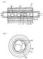
- the film forming apparatus 1includes a processing container 11, and a mounting table 12 for mounting the wafer W horizontally is provided in the processing container 11.
- a heater 13that serves as a temperature control means for the wafer W is provided.
- the mounting table 12is provided with three lifting pins 14a (only two are shown for convenience) that can be moved up and down by the lifting mechanism 14, and via the lifting pins 14a, a conveying means (not shown), the mounting table 12, and the like. The wafer W is transferred between the two. *
- the exhaust unit 16includes a pressure adjusting unit (not shown), and the exhaust amount is controlled in accordance with a control signal output from the control unit 100.
- a transfer port 17 that is opened and closed by a gate valve Gis formed on the side wall of the processing container 11. *
- a gas shower head 21is provided on the ceiling of the processing container 11 so as to face the mounting table 12.
- the gas shower head 21includes a partitioned gas chamber 22, and the gas supplied to the gas chamber 22 is distributed in the lower surface of the gas shower head 21 from a large number of gas supply holes 23 into the processing container 11. Supplied. *
- One end of a gas supply pipe 24is connected to the gas chamber 22, and the other end of the gas supply pipe 24 is SiH 4 that serves as a raw material for the polysilicon film via a flow rate control device group 25 including a valve and a mass flow controller. It is connected to a gas supply source 26 in which (monosilane) gas is stored.
- the flow rate control device group 25controls the supply / disconnection of the gas from the gas supply source 26 and a gas supply source described later to the wafer W in accordance with a control signal output from the control unit 100.
- a gas supply pipe 31is connected to the gas supply pipe 24, and the other end of the gas supply pipe 31 is connected to the cleaning gas through the filter 32, the energy supply unit 4, and the flow rate control device group 25 in this order.
- a gas supply source 33in which Cl 2 (chlorine) gas is stored.
- the gas flow path constituted by the gas supply pipes 24 and 31 and the flow rate control device group 25is made of stainless steel.
- the filter 32removes solid and liquid particles contained in the Cl 2 gas flowing through the gas supply pipe 31.
- the energy supply unit 4will be described later.
- the film forming apparatus 1includes a control unit 100 that controls operations of the heater 13, the exhaust unit 16, the flow rate control device group 25, and the like.
- the control unit 100includes, for example, a computer having a CPU and a program (not shown).
- the programincludes an operation necessary for performing the film forming process on the wafer W by the film forming apparatus 1, for example, the temperature of the wafer W by the heater 13.
- a group of steps (commands) for control, control of pressure in the processing container 11 and control related to adjustment of the supply amount of each gas into the processing container 11is set.
- This programis stored in a storage medium such as a hard disk, a compact disk, a magnetic optical disk, or a memory card, and installed in the computer therefrom.
- the energy supply unit 4that is, the stabilization reaction processing unit will be described with reference to FIG. FIG. 2A shows a longitudinal section of the energy supply unit 4, and FIG. 2B shows the energy supply unit 4 viewed from the opening direction.
- the energy supply unit 4includes an inner pipe 41 and an outer pipe 42 surrounding the inner pipe 41, and the inner pipe 41 is connected to the gas supply pipe 31.
- the gas supplied from the upstream side of the gas supply pipe 31 to the energy supply unit 4flows through the inner pipe 41 to the downstream side of the gas supply pipe 31.
- the inner tube 41is made of, for example, stainless steel, and the inner peripheral surface of the inner tube 41 is covered with a silicon film 43.
- a heater 44is provided in the space between the inner tube 41 and the outer tube 42 so as to surround the inner tube 41, and the gas passing through the inner tube 41 according to a control signal output from the control unit 100 is set at an arbitrary temperature. Can be heated.
- the inner tube 41is filled with a large number of balls 45 that are porous bodies.
- the ball 45 serving as a fillingis an obstacle in which a gas passing through the inner tube 41 collides, and the collision energy generated by the collision acts on the gas itself, and a compound containing halogen and metal contained in the gas. Is stabilized.
- the ball 45also serves as a capturing means for capturing the stabilized compound.
- the ball 45is made of alumina (aluminum oxide), which is a ceramic whose surface is coated with silicon.
- the diameter L1 of the ball 45is 3 mm, for example.
- the inner diameter L2 of the inner tube 41is, for example, 4.35 mm.
- the length L3 of the inner tube 41is, for example, 300
- the diameter L1 of the ball 45is preferably 50% to 87% of the inner diameter L2 of the inner tube 41 in order to cause the gas to collide with the ball 45 efficiently. Further, each ball 45 is arranged so that a part thereof is in contact with the silicon film 43 and the adjacent balls 45 are not completely overlapped with each other in the gas flow direction (the center position of each ball is shifted). It is desirable that
- the gate valve Gis opened, the wafer W is transferred into the processing container 11 by a transfer mechanism (not shown), and is placed on the mounting table 12 via the lift pins 14a, and the transfer mechanism is retracted from the processing container 11. To do. Thereafter, the gate valve G is closed, the wafer W is heated to a predetermined temperature by the heater 13, the inside of the processing container 11 is exhausted to a predetermined pressure, and then SiH 4 gas is supplied to the wafer W at a predetermined flow rate. Is done. The SiH 4 gas is decomposed by heat on the surface of the wafer W, and silicon is deposited on the surface of the wafer W to form a polysilicon film.
- the supply of the SiH 4 gasis stopped, and the wafer W is transferred to a transfer mechanism (not shown) by an operation reverse to that when the wafer W is loaded into the film forming apparatus 1. And then unloaded from the film forming apparatus 1.
- the heater 44 of the energy supply unit 4is heated to 150 ° C., for example, and Cl 2 gas is supplied from the gas supply source 33 toward the downstream side of the gas supply pipe 31.
- the Cl 2 gasis at room temperature, which is the temperature of the clean room where the film forming apparatus 1 is installed.
- the Cl 2 gasconstitutes the gas flow control device group 25 and the gas supply pipe 31 while passing through the flow path constituted by the flow control device group 25 and the gas supply pipe 31. It reacts with Cr (chromium) and O (oxygen) in stainless steel to produce CrO 2 Cl 2 .
- FIG. 4shows the vapor pressure curve of this CrO 2 Cl 2.
- the vapor pressure of CrO 2 Cl 2is relatively high.
- the pressure in the gas supply pipe 31is, for example, 0 kPa to 300 kPa. Since the CrO 2 Cl 2 is in a gaseous state at this pressure and the temperature of the clean room, the generated CrO 2 Cl 2 is in such a gaseous state. Then, it flows through the gas supply pipe 31 to the downstream side together with the Cl 2 gas and flows into the energy supply unit 4.
- the CrO 2 Cl 2 gas that has flowed into the energy supply unit 4advances downstream while colliding with the ball 45 in the inner tube 41 as shown in FIG. 3B.
- the collision energy generated by this collision and the thermal energy generated by the heater 44act on the CrO 2 Cl 2 gas, so that CrO 2 Cl 2 is reduced to CrCl 2 that is more stable as shown in FIG. Is done.
- the vapor pressure of CrCl 2is lower than the vapor pressure of CrO 2 Cl 2 , and at the temperature of the clean room and the pressure in the pipe.
- the reduced CrCl 2appears as a solid particle in the flow path of the inner tube 41.
- the ball 45is a porous body, CrCl 2 particles enter and are trapped in the ball 45, and the flow of the CrCl 2 particles to the downstream side is suppressed.
- the Cl 2 gas containing CrCl 2 particles that have passed through the group of balls 45flows from the energy supply unit 4 into the filter 32 on the downstream side. Then, as shown in FIG. 3D, the particles are captured by the filter 32 and removed from the Cl 2 gas. Then, the Cl 2 gas is supplied to the processing container 11 and reacts with Si adhering to the wall surface of the processing container 11 and the mounting table 12 to remove the Si. After a predetermined time has elapsed from the start of the supply of Cl 2 gas, the supply of Cl 2 gas is stopped and the heater 44 is cooled.
- the gas state metal compound generated by reacting with Cl 2is heated in the gas supply pipe 31 through which Cl 2 as a cleaning gas for cleaning the processing container 11 flows.
- An energy supply unit 4that is, a stabilization reaction processing unit, is provided that includes a heater 44 that supplies energy and a ball 45 that collides the metal compound to cause collision energy to act on the metal compound. Since the metal compound on which the energy has acted is stabilized and becomes a solid state and is captured by the group of balls 45, the supply of the metal compound to the processing container 11 is suppressed, and the inside of the processing container 11 and the wafer W are reduced. Metal contamination can be suppressed.
- a dummy waferis carried into the processing container 11 for processing, or before the processing of the wafer W, film formation is performed in the processing container. It is not necessary to perform a process that does not contribute to the production of the semiconductor device, such as performing the process, so that the throughput can be improved.
- a filter 32that captures the metal compound in a solid state and removes it from the Cl 2 gas is provided on the downstream side of the energy supply unit 4. Metal contamination of W can be suppressed.
- the inner surface of the inner pipe 41is covered with the silicon film 43, but the inner surface of the gas supply pipe 31 on the downstream side of the energy supply unit 4 may also be covered with the silicon film.
- the inner surface of the energy supply unit 4 and the downstream pipe thereofmay have higher corrosion resistance against Cl 2 gas than the inner surface of the upstream pipe of the energy supply unit 4, Corrosion at these parts can be suppressed, and metal contamination of the processing container 11 and the wafer W can be suppressed more reliably.
- the inner surface of the pipemay be made of silica, diamond-like carbon, alumina, fluorine resin, or the like instead of silicon.
- the energy supply unit 50 shown in FIG. 5includes an inner tube 51 instead of the inner tube 41, and the inner tube 51 is made of silicon so as to transmit ultraviolet rays.
- a UV lamp 52is provided in the outer tube 42 instead of providing the heater 44.
- the Cl 2 gasis supplied to the processing container 11, the UV light is irradiated to the Cl 2 gas passing through the inner tube 51 from the UV lamp 52.
- the aforementioned unstable high vapor pressure compound mixed in the Cl 2 gasis converted into a stable low vapor pressure stable compound.
- FIG. 6Ais a diagram showing still another example of the energy supply unit.
- a net-like member 54made of, for example, Pt (platinum) or Ni (nickel) is supported between the balls 45.
- FIG. 6Bshows the mesh member 54 viewed from the opening direction of the inner tube 41.
- the mesh member 54is in contact with the gas flowing through the inner pipe 41, thereby reducing the activation energy required for converting the compound having a high vapor pressure in the gas into the compound having the low vapor pressure described above. Play a role.
- the compound whose activation energy is reducedis converted into a stable compound by supplying thermal energy from the heater 44 and acting on collision energy to the ball 45.
- the aforementioned compoundcan be converted with lower energy than the above-described energy supply unit 4, so that metal contamination of the processing vessel 11 and the wafer W can be more reliably suppressed. .
- the catalystwhen the catalyst is used in this way, the catalyst may be formed in a ball shape instead of being formed in a net shape and filled in the inner tube 41.
- FIG. 6Cshows an example in which a ball 55 made of Pt is provided. In FIG. 6 (c), the ball 55 is shown with a number of points to distinguish it from the ball 45.
- FIG. 7shows another embodiment of the film forming apparatus, and the film forming apparatus 6 in FIG. 7 will be described focusing on the differences from the film forming apparatus 1.
- the exhaust pipe 15is connected to the exhaust port 15 a via an energy supply unit 60 configured similarly to the energy supply unit 4, that is, a stabilization reaction processing unit.
- an opening 61is provided in the side wall of the processing vessel 11, and a pipe 63 that forms an auxiliary flow path through the energy supply unit 62 that is configured similarly to the energy supply unit 4, that is, the stabilization reaction processing unit, in the opening 61.
- a pressure sensor 64which is an accessory device for measuring the degree of vacuum in the processing container 11.
- the exhaust pipe 15 and the pipe 63are made of stainless steel like the pipe 31.
- the gasmay diffuse along the pipe wall of the exhaust pipe 15 to the upstream side, that is, the processing container side.
- the energy supply unit 60when diffusion occurs in this way, it is possible to prevent the metal constituting the exhaust pipe 15 from being supplied to the processing container 11.
- the gasin the pipe 63 as well, the gas may diffuse from the pipe wall to the processing container 11 side like the exhaust pipe 15, and the gas is detected by the pressure sensor 64 due to the fluctuation of the pressure in the processing container 11 during the processing of the wafer W.
- diffusionmay occur from the side toward the processing container 11, even if such diffusion occurs, the metal constituting the pipe 63 is supplied to the processing container 11 by providing the energy supply unit 62. Can be prevented.
- the filter 32may be provided on the processing container 11 side as viewed from the energy supply unit 62 and the energy supply unit 60.
- the energy supply units 50 and 53 described abovemay be provided instead of the energy supply units 60 and 62. *
- the place where the heat energy or the light energy is supplied in the supply path of the gas containing halogenis the same as the place where the compound 45 is captured by the ball 45. .
- energy supply and compound capturemay be performed at different locations, and FIG. 8 (a) shows such an example.
- the energy supply unit 65 in this figureincludes a pipe 66 made of quartz, and the pipe 66 is interposed in the pipe 31 described above.
- the UV lamp 52supplies light energy to the gas flowing through the pipe 66.
- a filter 67 made of a net-like glass fiberis provided in the pipe 31 on the downstream side of the pipe 66, and captures the solid metal compound.
- control plates 68 and 69may be used to generate collision energy by collision with gas.
- the adjacent control plates 68 and 69are formed with through holes 68a and 69a so as not to overlap each other in the gas flow direction.
- the energy supply unit 4is provided as a processing apparatus in a film forming apparatus that is a semiconductor manufacturing apparatus.
- the semiconductor manufacturing apparatussupplies gas to the surface of an etching apparatus, a silicon wafer, etc.
- An epitaxial wafer manufacturing apparatus for epitaxially growing a crystal layer, an LED manufacturing apparatus, or the likemay be used, and the various energy supply units 4 described above can also be provided in these apparatuses.
- the semiconductor manufacturing apparatushere includes an FPD (flat panel display) manufacturing apparatus, a solar cell manufacturing apparatus, and an organic EL manufacturing apparatus, and each of the energy supply units described above can be provided in these apparatuses.
- the above-described various energy supply unitsthat is, stabilization reaction processing units, can be applied to all the processing apparatuses that supply gas to the processing container and perform processing on the object to be processed.
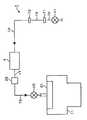
- Example 1The piping system 7 shown in FIG. 9 was connected to the processing container 11 described above.
- the pipe in which the filter 32 and the energy supply unit 4 are interposedis configured by connecting a flexible pipe and a hard pipe.
- reference numerals 71 and 72denote pipe connection portions.
- a new flexible piping having an inner peripheral surface made of stainless steelwas used in order to make it a source of metal contamination.
- piping 74 between the connection portion 72 and the energy supply portiona new flexible piping whose inner peripheral surface is made of stainless steel was used as the piping 74 between the connection portion 72 and the energy supply portion.
- a flexible piping whose inner peripheral surface is configured by silica coatingwas used as the piping 75 between the filter 32 and the valve V1 in the drawing.
- the lengths of the pipes 73, 74, and 75were 30 cm, 30 cm, and 50 cm, respectively.
- the valve V1 and the connecting portion 71 in the figure, and the energy supply portion 4 and the filter 32are connected by hard pipes 76 and 77, respectively, and the inner wall surface of the pipe 76 is made of stainless steel.
- the inner wall surface of the pipe 77is composed of a silica coat.
- the diameter of each pipeis 1/4 inch (6.35 mm).
- the reason why the inner peripheral surfaces of the pipes 75 and 77 are made of silica coatingis to suppress corrosion on the downstream side of the energy supply unit 4 as described above.
- silicathe above-described materials that can suppress corrosion can be used, but here silica was used.
- the gas cylinderwas removed, and an experimental apparatus was formed by connecting a gas supply system including an HBr gas supply source and an N 2 gas supply source upstream of the valve V1.
- the room in which this experimental apparatus is installedis at room temperature (22 ° C.).
- N 2 gas and HBr gascan be supplied to the processing vessel 11 via the piping system 7 respectively.
- a mass flow controller for controlling the flow rate of the HBr gas to the processing container 11is provided downstream of the HBr gas supply source.
- a plurality of N 2 gas supply sourcesare provided, and N 2 gas can be supplied to the processing container 11 at different flow rates.
- the temperature of the heater 44was set to 170 ° C. and the HBr gas was supplied to the processing container 11 at 200 sccm for 1 hour, and then the heater 44 was turned off and the HBr gas was supplied to the processing container 11 at 200 sccm for 25 minutes. .
- N 2 gasis supplied to the flow path, and then 500 cc of N 2 gas is supplied for 10 minutes.
- 500 cc of N 2 gasis supplied for 10 minutes.
- the processing container 11was purged by supplying N 2 gas to the processing container 11 at 500 cc per minute for one night. .
- the wafer W(referred to as “wafer W1” for convenience) is loaded into the processing container 11 according to the above-described embodiment, and the inside of the processing container 11 is evacuated (the evacuation after loading the wafer W is “step A”). to), and the N 2 gas is supplied into the processing chamber 11 per minute 500cc from N 2 gas supply source. At this time, the power supply of the heater 44 is turned off, and thus the heater 44 is at the room temperature of 22 ° C. Then, with the pressure in the processing container 11 maintained at 50 kPa, the gas supplied to the processing container 11 is gradually switched from N 2 gas to HBr gas over 5 minutes. After switching, the HBr gas is changed to 100 sccm for 1 hour. , And supplied to the processing container 11.
- Step Bthe wafer W1 was taken out of the processing container 11, and the amounts of Fe and Cr attached to the wafer W1 were measured by ICP mass spectrometry.
- Example 2After unloading the wafer W1 from the processing container 11 in the first embodiment, another wafer W (referred to as “wafer W2” for convenience) is loaded while the N 2 gas is being supplied.
- the process up to Step Bwas performed. However, the temperature of the heater 44 was set to 150 ° C. when the HBr gas was supplied.
- the wafer W2was taken out of the processing container 11, and the amounts of Fe and Cr attached to the wafer W2 were measured by ICP mass spectrometry.
- Example 3Experiments were performed in substantially the same procedure as in Example 1, using an apparatus constituted by the same piping system 7 and gas supply system as in Example 1. However, the filter 32 is not provided in the piping system 7.
- the temperature of the heater 44is set to 370 ° C. and the inside of the processing container 11 is maintained at 50 kPa, and N 2 gas supply source is supplied at 500 cc / min for 45 minutes. Two gases were supplied, and the processing vessel 11 was purged. Then the temperature of the heater 44 to 300 ° C., subsequently maintaining the process chamber 11 to 50 kPa, 15 minutes per minute 500sccm from N 2 gas supply source, performs the supply of the N 2 gas was purged process vessel 11 .
- the wafer W(referred to as “wafer W3” for convenience) was loaded into the processing container 11, the inside of the processing container 11 was evacuated, and the processing from Step A to Step B was performed in the same manner as in Example 1.
- the temperature of the heater 44is 300 ° C. after supplying the N 2 gas to the processing container 11 at 500 cc / min until supplying the HBr gas to the processing container 11.
- the wafer W3was taken out of the processing container 11, and the amount of Fe and Cr attached to the wafer W3 was measured by ICP mass spectrometry.
- the heater 44was turned off and the heater 44 was cooled.
- Example 4After the wafer W3 is unloaded from the processing container 11 in the third embodiment, another wafer W (referred to as “wafer W4” for convenience) is loaded while the N 2 gas is being supplied. Processing up to B was performed. However, the temperature of the heater 44 was set to 35 ° C. when the HBr gas was supplied. After switching the atmosphere of the processing container 11 in Step B, the wafer W4 was taken out of the processing container 11, and the amounts of Fe and Cr attached to the wafer W4 were measured by ICP mass spectrometry.
- Comparative Example 1The experiment was performed in the same procedure as in Example 1. However, in Comparative Example 1, the energy supply unit 4 was not provided in the piping system 7.
- Table 1is a table showing the results of the examples and comparative examples.
- the detection limit of Cr in the apparatus for performing ICP mass spectrometryis 0.074 ⁇ 1e 10 atoms / cm 2 .
- the detection value of Crwas not more than the detection limit value.
- the detected value of Fe in Example 1is 0.38 ⁇ 1e 10 atoms / cm 2 .
- the detected values of Cr and Fe of the comparative exampleare 12 ⁇ 1e 10 atoms / cm 2 and 55 ⁇ 1e 10 atoms / cm 2 , respectively.
- the detected values of Cr and Fe of Example 1are the same as those of Comparative Example 1. Since it was lower than the detected value, the effect of the present invention was shown.
- the stabilization reaction processing section(6, 60, 62, 65) is configured as an energy supply section having an energy generator for supplying heat energy and light energy from the outside, but the present invention is not limited thereto.
- a stabilization reaction processing unitthat stabilizes a compound containing a halogen and a metal can be configured.
- Example 2since the detection amount of Cr and Fe was small compared with the comparative example 1, the effect of this invention was proved.
- Example 3the detected amounts of Cr and Fe were smaller than those in Comparative Example 1. From this, it was shown that even if the filter 32 is not provided, the compounds each composed of Cr and Fe are captured in the balls 45 of the energy supply unit 4 and the supply of these metals to the processing container 11 is suppressed. Further, in Example 4, as in Example 3, since the detected amounts of Cr and Fe were smaller than in Comparative Example 1, it was shown that the compound could be removed without the filter 32 as well.
Landscapes
- Chemical & Material Sciences (AREA)
- General Chemical & Material Sciences (AREA)
- Chemical Kinetics & Catalysis (AREA)
- Engineering & Computer Science (AREA)
- Materials Engineering (AREA)
- Mechanical Engineering (AREA)
- Metallurgy (AREA)
- Organic Chemistry (AREA)
- Electrochemistry (AREA)
- Chemical Vapour Deposition (AREA)
- Drying Of Semiconductors (AREA)
Abstract
Description
本発明は、被処理体に対して処理を行う処理装置に関する。The present invention relates to a processing apparatus for processing a target object.
半導体装置の製造工程には、半導体ウエハ(以下ウエハという)にガスを供給して、例えばCVD(Chemical Vapor Deposition)により成膜を行う工程や、ウエハにガスを供給し、そのガスによりウエハ表面の膜をエッチングする工程がある。このような工程を行う成膜またはエッチング装置は、ウエハを収納する処理容器と、成膜またはエッチング工程で用いられる処理ガスの貯留部と、処理容器内をドライクリーニングするためのクリーニングガスの貯留部と、を備えており、各ガスの貯留部と前記処理容器とが、ガス供給配管およびこの配管に介設されるバルブなどを備えたガス供給機器により接続されている。In the manufacturing process of a semiconductor device, a gas is supplied to a semiconductor wafer (hereinafter referred to as a wafer) and a film is formed by, for example, CVD (Chemical Vapor Deposition), or a gas is supplied to the wafer, and the gas is used to form a wafer surface. There is a step of etching the film. A film forming or etching apparatus that performs such a process includes a processing container for storing a wafer, a processing gas storing unit used in the film forming or etching process, and a cleaning gas storing unit for dry cleaning the processing container. The gas storage section and the processing container are connected by a gas supply device including a gas supply pipe and a valve interposed in the pipe.
高い耐腐食性を得るために前記ガス供給機器は、例えばステンレス鋼により構成される。また、前記ガス供給配管にはガス中に含まれる固体及び液体のパーティクル(粒子)を除去するためのフィルタが介設される場合がある。In order to obtain high corrosion resistance, the gas supply device is made of, for example, stainless steel. The gas supply pipe may be provided with a filter for removing solid and liquid particles contained in the gas.
このような成膜装置またはエッチング装置では、夫々F(フッ素)、Cl(塩素)、Br(臭素)を含んだF系ガス、Cl系ガス、Br系ガスと呼ばれる、ハロゲンを含む非常に反応性の高いガスが用いられる場合がある。例えば前記F系ガスは前記成膜装置におけるクリーニング用ガスとして用いられる場合があり、例えばCl系ガス及びBr系ガスは前記エッチング装置においてエッチング用ガスとして用いられる場合がある。 In such a film-forming apparatus or etching apparatus, they are extremely reactive including halogen, called F-based gas, Cl-based gas, and Br-based gas containing F (fluorine), Cl (chlorine), and Br (bromine), respectively. A high gas may be used. For example, the F-based gas may be used as a cleaning gas in the film forming apparatus. For example, a Cl-based gas and a Br-based gas may be used as an etching gas in the etching apparatus. *
これらのハロゲンを含むガスは、そのガスを供給するためのガス供給機器を構成するステンレス鋼と反応し、ハロゲン、金属及び酸素からなる3元系化合物およびハロゲン及び金属からなる2元系化合物が生成し、それらの化合物によるガスの金属汚染が起きてしまう。これらの3元系化合物及び2元系化合物には蒸気圧が高いものがあり、そのような化合物は配管内を気体の状態で流通するため、前記フィルタに捕捉されずに処理容器内に供給される。そして、これらの3元系化合物及び2元系化合物が処理容器内の雰囲気に曝されて分解して、それらの化合物に含まれる金属が固体となってウエハ及び処理容器内に付着する場合がある。そうなると、ウエハが正常に処理されなくなり、歩留りが低下してしまうおそれがある。These halogen-containing gases react with the stainless steel that constitutes the gas supply equipment for supplying the gas to produce ternary compounds composed of halogen, metal and oxygen and binary compounds composed of halogen and metal. In addition, metal contamination of the gas by these compounds occurs. Some of these ternary compounds and binary compounds have high vapor pressures, and such compounds circulate in the state of gas in the pipe, and are thus supplied to the processing vessel without being captured by the filter. The Then, these ternary compounds and binary compounds are decomposed by exposure to the atmosphere in the processing container, and the metal contained in these compounds may become solid and adhere to the wafer and the processing container. . If so, the wafer may not be processed normally, and the yield may be reduced.
また、処理容器に供給されたガスは、処理容器を排気するための排気管内に流入する。排気管内が気体の圧力が高い低真空域となり、気体分子同士の衝突が気体分子と排気管の管壁との衝突に比べて優勢であるとき、排気管内の気体の流速は、排気管の中心軸におけおいて最も高く、中心軸から排気管の管壁に近づくほど低くなり、管壁では0になる。流速が0となった管壁に沿ってガスが上流側、つまり処理容器側に拡散してしまう場合がある。このような処理容器内への気体の拡散が生じたとき、上記の気体状態の3元系化合物及び2元系化合物が、固体の金属を含む化合物に変化してウエハや処理容器内に付着し、歩留りが低下するおそれもある。さらに、処理容器には補助流路を介して真空計などの付属機器が取り付けられる場合がある。補助流路を構成する配管においても排気管と同様に流速が0になる管壁から処理容器側にガスが拡散することがあるし、またウエハの処理中に処理容器内の圧力の変動によって、ガスが付属機器側から処理容器側に向けて拡散することがある。そのように補助流路からガスが拡散したときにも、気体状態の3元系化合物及び2元系化合物が、固体の金属を含む化合物に変化してウエハや処理容器内に付着するおそれがある。Also, the gas supplied to the processing container flows into the exhaust pipe for exhausting the processing container. When the inside of the exhaust pipe is in a low vacuum region where the gas pressure is high and collisions between gas molecules are dominant compared to collisions between gas molecules and the pipe wall of the exhaust pipe, the flow velocity of the gas in the exhaust pipe is the center of the exhaust pipe. It is the highest on the shaft, and becomes lower as it approaches the tube wall of the exhaust pipe from the central shaft, and becomes 0 on the tube wall. There is a case where the gas diffuses to the upstream side, that is, the processing container side along the tube wall where the flow velocity becomes zero. When such gas diffusion into the processing container occurs, the above-described ternary compound and binary compound in the gaseous state change into a compound containing a solid metal and adhere to the wafer or the processing container. There is also a risk that the yield is lowered. Furthermore, an accessory device such as a vacuum gauge may be attached to the processing container via an auxiliary flow path. In the piping constituting the auxiliary flow path, gas may diffuse from the tube wall where the flow velocity becomes 0 similarly to the exhaust pipe to the processing container side, and also due to fluctuations in pressure in the processing container during wafer processing, Gas may diffuse from the accessory side toward the processing vessel. Even when the gas diffuses from the auxiliary flow path, the ternary compound and the binary compound in a gas state may be changed to a compound containing a solid metal and adhere to the wafer or the processing container. .
上記の現象に起因する歩留りの低下を防ぐために、上記のハロゲンを含むガスを処理容器内に供給した後は、ダミーウエハ(製品ウエハではないウエハ)を処理容器内に搬送し、そのダミーのウエハにエッチングまたは成膜処理を行い、そのダミーのウエハに前記金属を付着させて処理容器内から除去した後に通常のウエハを処理容器内に搬送して、改めてエッチングや成膜処理を行う場合がある。或いは、処理容器内に所定のガスを供給し、処理容器の壁面に付着した金属を覆ってこの金属の飛散を防止する膜を成膜した後、処理容器内にウエハを搬送して処理を行う場合もある。しかし、ダミーウエハを用いる場合も、処理容器内に飛散防止膜を成膜する場合も、半導体の製造に寄与しない処理が行われるので、スループットが低下することになるし、処理コストも高くなってしまう。In order to prevent a decrease in yield due to the above phenomenon, after supplying the halogen-containing gas into the processing container, a dummy wafer (wafer that is not a product wafer) is transferred into the processing container, and the dummy wafer is transferred to the dummy wafer. In some cases, etching or film formation is performed, the metal is attached to the dummy wafer and removed from the processing container, and then a normal wafer is transferred into the processing container to perform etching or film formation again. Alternatively, a predetermined gas is supplied into the processing container, a film that covers the metal adhering to the wall surface of the processing container and prevents the metal from being scattered is formed, and then the wafer is transferred into the processing container for processing. In some cases. However, even when a dummy wafer is used or when an anti-scattering film is formed in a processing container, processing that does not contribute to semiconductor manufacturing is performed, resulting in a decrease in throughput and an increase in processing cost. .
日本国特許出願公開公報特開2002-222807号(JP2002-222807A)には、ウエハの金属汚染を抑制するためにクロム酸化物によりガスに接する金属製部材をコーティングすることについて記載されている。しかし、上記のハロゲン含有ガスはクロム酸化物と反応するので、上記の問題を解決することはできない。Japanese Patent Application Publication No. 2002-222807 (JP2002-222807A) describes coating a metal member in contact with a gas with chromium oxide in order to suppress metal contamination of a wafer. However, since the above halogen-containing gas reacts with chromium oxide, the above problem cannot be solved.
本発明は、被処理体に対して処理を行うための処理容器を備えた処理装置において、処理容器及び被処理体の金属汚染を防ぐことができる処理装置を提供する。The present invention provides a processing apparatus including a processing container for performing processing on an object to be processed, which can prevent metal contamination of the processing container and the object to be processed.
本発明の第1の観点によれば、被処理体に対して処理を行うための処理容器を備えた処理装置において、少なくとも一部が金属により構成され、ハロゲンを含む腐食性ガスを前記処理容器に供給するためのガス供給流路と、前記ガス供給流路における金属部分を通流した前記腐食性ガスに光エネルギーまたは熱エネルギーを供給するエネルギー発生器、および前記ガス供給流路における金属部分を通流した前記腐食性ガスを衝突させることにより前記腐食性ガスに作用する衝突エネルギーを発生させるように設けられた障害物のうちの少なくとも一つを有し、前記光エネルギー、熱エネルギーおよび衝突エネルギーのうちの少なくとも一つにより前記腐食性ガスに含まれるハロゲンと前記金属とを含む化合物を安定化させる反応が行われる安定化反応処理部と、前記安定化反応処理部において安定化された化合物を捕捉する捕捉手段と、を備えた処理装置が提供される。According to a first aspect of the present invention, in a processing apparatus provided with a processing container for performing processing on an object to be processed, corrosive gas containing at least a part of metal and containing halogen is supplied to the processing container. A gas supply channel for supplying to the gas, an energy generator for supplying light energy or thermal energy to the corrosive gas flowing through the metal part in the gas supply channel, and a metal part in the gas supply channel It has at least one of obstacles provided to generate collision energy that acts on the corrosive gas by colliding with the corrosive gas that has flowed through, and the light energy, thermal energy, and collision energy. The reaction for stabilizing the compound containing halogen and the metal contained in the corrosive gas is performed by at least one of And Joka reaction processor, a capture means for capturing a stabilized compound, with a processing device is provided in the stabilizing reaction unit.
好ましくは、前記ガス供給流路において、前記光エネルギー、熱エネルギーおよび衝突エネルギーのうちの少なくとも一つが作用する部位または当該部位の下流側の流路を構成する壁面は、前記部位の上流側の流路を構成する壁面よりも前記腐食性ガスに対する耐腐食性が高い。その場合、前記部位の流路を構成する壁面または前記部位の下流側の流路を構成する壁面はシリコン、シリカ、ダイヤモンド・ライク・カーボン、アルミナまたはフッ素樹脂のいずれかにより構成することができる。Preferably, in the gas supply flow path, the part on which at least one of the light energy, the thermal energy, and the collision energy acts or the wall surface constituting the flow path on the downstream side of the part is a flow on the upstream side of the part. Corrosion resistance to the corrosive gas is higher than that of the wall surface constituting the road. In that case, the wall surface constituting the flow path of the part or the wall surface constituting the flow path on the downstream side of the part can be made of any of silicon, silica, diamond-like carbon, alumina, or fluororesin.
本発明の第2の観点によれば、被処理体に対して処理を行うための処理容器を備え、この処理容器にはハロゲンを含む腐食性ガスが供給される処理装置において、前記処理容器に接続され、少なくとも一部が金属により構成された排気流路と、前記排気流路における金属部分から処理容器に向けて拡散したガスに光エネルギーまたは熱エネルギーを供給するエネルギー発生器、および前記排気流路における金属部分から処理容器に向けて拡散したガスを衝突させることにより当該ガスに作用する衝突エネルギーを発生させるように設けられた障害物のうちの少なくとも一つを有し、前記光エネルギー、熱エネルギーおよび衝突エネルギーのうちの少なくとも一つにより前記排気流路内のガスに含まれるハロゲンと前記金属とを含む化合物を安定化させる反応が行われる安定化反応処理部と、前記安定化反応処理部において安定化された化合物を捕捉する捕捉手段と、を備えた処理装置が提供される。According to a second aspect of the present invention, a processing container for performing processing on an object to be processed is provided. In the processing apparatus in which a corrosive gas containing halogen is supplied to the processing container, An exhaust flow path connected and at least partially made of metal, an energy generator for supplying light energy or thermal energy to a gas diffused from the metal portion in the exhaust flow path toward the processing container, and the exhaust flow Having at least one of obstacles provided to generate collision energy acting on the gas by colliding with the gas diffused from the metal part in the path toward the processing container, the light energy, the heat A compound containing halogen and the metal contained in the gas in the exhaust passage by at least one of energy and collision energy And stabilization reaction unit which the reaction is carried out to Joka, a capture means for capturing a stabilized compound, with a processing device is provided in the stabilizing reaction unit.
本発明の第3の観点によれば、被処理体に対して処理を行うための処理容器を備え、この処理容器にはハロゲンを含む腐食性ガスが供給される処理装置において、付属機器を取り付けるために前記処理容器に接続され、少なくとも一部が金属により構成された補助流路と、前記補助流路における金属部分から処理容器に向けて拡散したガスに光エネルギーまたは熱エネルギーを供給するエネルギー発生器、および前記補助流路における金属部分から処理容器に向けて拡散したガスを衝突させることにより当該ガスに作用する衝突エネルギーを発生させるように設けられた障害物のうちの少なくとも一つを有し、前記光エネルギー、熱エネルギーおよび衝突エネルギーのうちの少なくとも一つにより前記補助流路内のガスに含まれるハロゲンと前記金属とを含む化合物を安定化させる反応が行われる安定化反応処理部と、前記安定化反応処理部において安定化された化合物を捕捉する捕捉手段と、を備えたことを特徴とする処理装置が提供される。According to the third aspect of the present invention, a processing container for performing processing on an object to be processed is provided, and an accessory device is attached to the processing container in which a corrosive gas containing halogen is supplied. For this purpose, an auxiliary flow path that is connected to the processing vessel and is at least partially made of metal, and energy generation that supplies light energy or thermal energy to the gas diffused from the metal portion of the auxiliary flow channel toward the processing vessel And at least one of obstacles provided to generate collision energy acting on the gas by colliding gas diffused from the metal portion in the auxiliary flow path toward the processing vessel , Halogen contained in the gas in the auxiliary flow path by at least one of the light energy, thermal energy, and collision energy A processing apparatus comprising: a stabilization reaction processing unit in which a reaction for stabilizing a compound containing the metal is performed; and a capture unit that captures the compound stabilized in the stabilization reaction processing unit. Is provided.
前記安定化反応処理部に、前記障害物として、前記流路内に充填された非金属からなる充填物を設けることができる。この場合、前記充填物は、前記捕捉手段としの機能も持たせることができる。また、好適な一実施形態においては、前記充填物は、セラミックスからなる球状体の群であり、この場合、前記充填物を加熱するための加熱手段及び前記充填物に光を照射する光照射手段の少なくとも一方を設けることができる。さらに、前記充填物には、前記化合物を安定化させるための触媒が担持されていてもよい。In the stabilization reaction processing section, a filling made of a nonmetal filled in the flow path can be provided as the obstacle. In this case, the filling can also have a function as the capturing means. In a preferred embodiment, the filler is a group of spherical bodies made of ceramics. In this case, a heating means for heating the filler and a light irradiation means for irradiating the filler with light. At least one of the above can be provided. Furthermore, the packing may support a catalyst for stabilizing the compound.
本発明によれば、安定化反応処理部および捕捉手段により、処理容器及び被処理体の金属汚染を防ぐことができる。According to the present invention, metal contamination of the processing container and the object to be processed can be prevented by the stabilization reaction processing unit and the capturing means.
処理装置の一例としてCVDによりポリシリコン(多結晶シリコン)膜をウエハWに形成する成膜装置1について、その縦断側面図である図1を参照しながら説明する。成膜装置1は処理容器11を備えており、処理容器11内には、ウエハWを水平に載置するための載置台12が設けられている。載置台12内にはウエハWの温調手段をなすヒータ13が設けられている。更に載置台12には、昇降機構14により昇降自在な3本の昇降ピン14a(便宜上2本のみ図示)が設けられており、この昇降ピン14aを介して不図示の搬送手段と載置台12との間でウエハWの受け渡しが行われる。 As an example of the processing apparatus, afilm forming apparatus 1 for forming a polysilicon (polycrystalline silicon) film on a wafer W by CVD will be described with reference to FIG. Thefilm forming apparatus 1 includes aprocessing container 11, and a mounting table 12 for mounting the wafer W horizontally is provided in theprocessing container 11. In the mounting table 12, aheater 13 that serves as a temperature control means for the wafer W is provided. Further, the mounting table 12 is provided with three liftingpins 14a (only two are shown for convenience) that can be moved up and down by thelifting mechanism 14, and via the lifting pins 14a, a conveying means (not shown), the mounting table 12, and the like. The wafer W is transferred between the two. *
処理容器11の底部の排気口15aには排気管15の一端側が接続され、この排気管15の他端側には真空ポンプにより構成される排気手段16が接続されている。排気手段16は不図示の圧力調整手段を備えており、制御部100から出力される制御信号に応じて排気量が制御される。また、処理容器11の側壁には、ゲートバルブGにより開閉される搬送口17が形成されている。 One end side of theexhaust pipe 15 is connected to theexhaust port 15a at the bottom of theprocessing vessel 11, and the exhaust means 16 constituted by a vacuum pump is connected to the other end side of theexhaust pipe 15. Theexhaust unit 16 includes a pressure adjusting unit (not shown), and the exhaust amount is controlled in accordance with a control signal output from thecontrol unit 100. Atransfer port 17 that is opened and closed by a gate valve G is formed on the side wall of theprocessing container 11. *
さらに処理容器11の天井部には、載置台12に対向するようにガスシャワーヘッド21が設けられている。ガスシャワーヘッド21は、区画されたガス室22を備え、ガス室22に供給されたガスは、ガスシャワーヘッド21の下面に分散して穿孔された多数のガス供給孔23から処理容器11内に供給される。 Furthermore, agas shower head 21 is provided on the ceiling of theprocessing container 11 so as to face the mounting table 12. Thegas shower head 21 includes a partitionedgas chamber 22, and the gas supplied to thegas chamber 22 is distributed in the lower surface of thegas shower head 21 from a large number of gas supply holes 23 into theprocessing container 11. Supplied. *
ガス室22にはガス供給配管24の一端が接続されており、ガス供給配管24の他端は、バルブやマスフローコントローラを備えた流量制御機器群25を介してポリシリコン膜の原料となるSiH4(モノシラン)ガスが貯留されたガス供給源26に接続されている。流量制御機器群25は、制御部100から出力される制御信号に従ってガス供給源26と後述のガス供給源からの各ガスのウエハWへの給断を制御する。 One end of agas supply pipe 24 is connected to thegas chamber 22, and the other end of thegas supply pipe 24 is SiH4 that serves as a raw material for the polysilicon film via a flow ratecontrol device group 25 including a valve and a mass flow controller. It is connected to agas supply source 26 in which (monosilane) gas is stored. The flow ratecontrol device group 25 controls the supply / disconnection of the gas from thegas supply source 26 and a gas supply source described later to the wafer W in accordance with a control signal output from thecontrol unit 100.
また、ガス供給配管24にはガス供給配管31の一端が接続されており、ガス供給配管31の他端はフィルタ32、エネルギー供給部4、前記流量制御機器群25をこの順に介して、クリーニングガスであるCl2(塩素)ガスが貯留されたガス供給源33に接続されている。ガス供給配管24、31及び流量制御機器群25により構成されるガス流路はステンレス鋼により構成されている。フィルタ32は、ガス供給配管31を流通するCl2ガス中に含まれる固体及び液体のパーティクルを除去する。エネルギー供給部4については後述する。 In addition, one end of agas supply pipe 31 is connected to thegas supply pipe 24, and the other end of thegas supply pipe 31 is connected to the cleaning gas through thefilter 32, theenergy supply unit 4, and the flow ratecontrol device group 25 in this order. Is connected to agas supply source 33 in which Cl2 (chlorine) gas is stored. The gas flow path constituted by thegas supply pipes control device group 25 is made of stainless steel. Thefilter 32 removes solid and liquid particles contained in the Cl2 gas flowing through thegas supply pipe 31. Theenergy supply unit 4 will be described later.
成膜装置1は、ヒータ13、排気手段16及び流量制御機器群25などの動作を制御する制御部100を備えている。制御部100は例えば図示しないCPUとプログラムとを備えたコンピュータからなり、プログラムには当該成膜装置1によってウエハWへの成膜処理を行うのに必要な動作、例えばヒータ13によるウエハWの温度のコントロールや処理容器11内の圧力調整及び処理容器11内への各ガスの供給量調整に係る制御等についてのステップ(命令)群が組まれている。このプログラムは、例えばハードディスク、コンパクトディスク、マグネットオプティカルディスク、メモリーカード等の記憶媒体に格納され、そこからコンピュータにインストールされる。Thefilm forming apparatus 1 includes acontrol unit 100 that controls operations of theheater 13, theexhaust unit 16, the flow ratecontrol device group 25, and the like. Thecontrol unit 100 includes, for example, a computer having a CPU and a program (not shown). The program includes an operation necessary for performing the film forming process on the wafer W by thefilm forming apparatus 1, for example, the temperature of the wafer W by theheater 13. A group of steps (commands) for control, control of pressure in theprocessing container 11 and control related to adjustment of the supply amount of each gas into theprocessing container 11 is set. This program is stored in a storage medium such as a hard disk, a compact disk, a magnetic optical disk, or a memory card, and installed in the computer therefrom.
続いて、エネルギー供給部4すなわち安定化反応処理部について図2を参照しながら説明する。図2(a)はエネルギー供給部4の縦断面を示しており、図2(b)はエネルギー供給部4をその開口方向から見た図である。このエネルギー供給部4は、内管41とその内管41を囲う外管42とを備えており、内管41はガス供給配管31に接続されている。そして、ガス供給配管31の上流側からエネルギー供給部4に供給されたガスは、この内管41内を通ってガス供給配管31の下流側へ流通する。内管41は例えばステンレス鋼により構成されており、内管41の内周面はシリコン膜43により被覆されている。Subsequently, theenergy supply unit 4, that is, the stabilization reaction processing unit will be described with reference to FIG. FIG. 2A shows a longitudinal section of theenergy supply unit 4, and FIG. 2B shows theenergy supply unit 4 viewed from the opening direction. Theenergy supply unit 4 includes aninner pipe 41 and anouter pipe 42 surrounding theinner pipe 41, and theinner pipe 41 is connected to thegas supply pipe 31. The gas supplied from the upstream side of thegas supply pipe 31 to theenergy supply unit 4 flows through theinner pipe 41 to the downstream side of thegas supply pipe 31. Theinner tube 41 is made of, for example, stainless steel, and the inner peripheral surface of theinner tube 41 is covered with asilicon film 43.
内管41と外管42との間の空間には当該内管41を囲うヒータ44が設けられており、制御部100から出力される制御信号に従って内管41内を通過するガスを任意の温度に加熱することができる。また、内管41内には多孔質体である多数のボール45が充填されている。充填物であるボール45は、内管41内を通過するガスが衝突する障害物であり、この衝突によって発生した衝突エネルギーがガス自体に作用して、ガス中に含まれるハロゲンおよび金属を含む化合物が安定化される。またボール45は、安定化した化合物を捕捉する捕捉手段を兼ねている。ボール45は、その表面をシリコンにより被覆されたセラミックスであるアルミナ(酸化アルミニウム)により構成されている。この例では、このボール45の直径L1は例えば3mmである。また内管41の内径L2は例えば4.35mmである。また、内管41の長さL3は例えば300mmである。Aheater 44 is provided in the space between theinner tube 41 and theouter tube 42 so as to surround theinner tube 41, and the gas passing through theinner tube 41 according to a control signal output from thecontrol unit 100 is set at an arbitrary temperature. Can be heated. Theinner tube 41 is filled with a large number ofballs 45 that are porous bodies. Theball 45 serving as a filling is an obstacle in which a gas passing through theinner tube 41 collides, and the collision energy generated by the collision acts on the gas itself, and a compound containing halogen and metal contained in the gas. Is stabilized. Theball 45 also serves as a capturing means for capturing the stabilized compound. Theball 45 is made of alumina (aluminum oxide), which is a ceramic whose surface is coated with silicon. In this example, the diameter L1 of theball 45 is 3 mm, for example. The inner diameter L2 of theinner tube 41 is, for example, 4.35 mm. Further, the length L3 of theinner tube 41 is, for example, 300 mm.
ボール45の直径L1は、ガスを効率よくボール45に衝突させるために、前記内管41の内径L2の50%~87%の大きさであることが好ましい。さらに、各ボール45は、その一部が前記シリコン膜43に接すると共に、ガスの流方向に対して隣り合うボール45同士が完全に重なり合わないように(各ボールの中心位置をずらして)配置されることが望ましい。The diameter L1 of theball 45 is preferably 50% to 87% of the inner diameter L2 of theinner tube 41 in order to cause the gas to collide with theball 45 efficiently. Further, eachball 45 is arranged so that a part thereof is in contact with thesilicon film 43 and theadjacent balls 45 are not completely overlapped with each other in the gas flow direction (the center position of each ball is shifted). It is desirable that
続いて成膜装置1の作用について説明する。先ず、ゲートバルブGが開き、ウエハWが不図示の搬送機構により処理容器11内に搬送されて、昇降ピン14aを介して載置台12に載置されると共に搬送機構が処理容器11内から退避する。その後、ゲートバルブGが閉じられ、ヒータ13によりウエハWが所定の温度に加熱され、処理容器11内が排気されて所定の圧力になった後、所定の流量でSiH4ガスがウエハWに供給される。SiH4ガスはウエハWの表面で熱により分解し、ウエハW表面にシリコンが堆積して、ポリシリコン膜が形成される。Next, the operation of thefilm forming apparatus 1 will be described. First, the gate valve G is opened, the wafer W is transferred into theprocessing container 11 by a transfer mechanism (not shown), and is placed on the mounting table 12 via the lift pins 14a, and the transfer mechanism is retracted from theprocessing container 11. To do. Thereafter, the gate valve G is closed, the wafer W is heated to a predetermined temperature by theheater 13, the inside of theprocessing container 11 is exhausted to a predetermined pressure, and then SiH4 gas is supplied to the wafer W at a predetermined flow rate. Is done. The SiH4 gas is decomposed by heat on the surface of the wafer W, and silicon is deposited on the surface of the wafer W to form a polysilicon film.
SiH4ガスの供給開始から所定の時間経過後、SiH4ガスの供給が停止し、ウエハWは成膜装置1に搬入されたときとは逆の動作により、不図示の搬送機構に受け渡されて成膜装置1から搬出される。After a predetermined time has elapsed from the start of the supply of the SiH4 gas, the supply of the SiH4 gas is stopped, and the wafer W is transferred to a transfer mechanism (not shown) by an operation reverse to that when the wafer W is loaded into thefilm forming apparatus 1. And then unloaded from thefilm forming apparatus 1.
これ以降、図3の配管内における変化の模式図を参照しながら説明する。ウエハW搬出後、エネルギー供給部4のヒータ44が例えば150℃に昇温し、ガス供給源33からCl2ガスがガス供給配管31の下流側に向けて供給される。このとき、Cl2ガスは成膜装置1が据え付けられたクリーンルームの温度である常温になっている。図3(a)に示すようにCl2ガスは、流量制御機器群25及びガス供給配管31により構成される流路を通流中にこれらガス流量制御機器群25及びガス供給配管31を構成するステンレス鋼中のCr(クロム)及びO(酸素)と反応し、CrO2Cl2が生成する。Hereinafter, description will be made with reference to the schematic diagram of the change in the piping of FIG. After the wafer W is unloaded, theheater 44 of theenergy supply unit 4 is heated to 150 ° C., for example, and Cl2 gas is supplied from thegas supply source 33 toward the downstream side of thegas supply pipe 31. At this time, the Cl2 gas is at room temperature, which is the temperature of the clean room where thefilm forming apparatus 1 is installed. As shown in FIG. 3A, the Cl2 gas constitutes the gas flowcontrol device group 25 and thegas supply pipe 31 while passing through the flow path constituted by the flowcontrol device group 25 and thegas supply pipe 31. It reacts with Cr (chromium) and O (oxygen) in stainless steel to produce CrO2 Cl2 .
図4にはこのCrO2Cl2の蒸気圧曲線を示しているが、この図に示されるようにCrO2Cl2の蒸気圧は比較的高い。ガス供給配管31内の圧力は例えば0kPa~300kPaであり、この圧力及び前記クリーンルームの温度において当該CrO2Cl2は気体の状態であるため、生成したCrO2Cl2は、そのように気体の状態でCl2ガスと共にガス供給配管31を下流側へと流通し、エネルギー供給部4に流れ込む。FIG. 4 shows the vapor pressure curve of this CrO2 Cl2. As shown in this figure, the vapor pressure of CrO2 Cl2 is relatively high. The pressure in thegas supply pipe 31 is, for example, 0 kPa to 300 kPa. Since the CrO2 Cl2 is in a gaseous state at this pressure and the temperature of the clean room, the generated CrO2 Cl2 is in such a gaseous state. Then, it flows through thegas supply pipe 31 to the downstream side together with the Cl2 gas and flows into theenergy supply unit 4.
そして、エネルギー供給部4に流れ込んだCrO2Cl2ガスは、図3(b)に示すようにその内管41内をボール45に衝突しながら下流側へ進む。この衝突により生じた衝突エネルギーとヒータ44が発生する熱エネルギーがCrO2Cl2ガスに作用することにより、図3(c)に示すようにCrO2Cl2はそれよりも安定なCrCl2に還元される。ここで、図4に示したCrCl2の蒸気圧曲線から明らかなように、CrCl2の蒸気圧はCrO2Cl2の蒸気圧よりも低く、上記のクリーンルームの温度及び上記の配管内の圧力において、還元されたCrCl2は固体のパーティクルとなって内管41の流路に現れる。既述のようにボール45は多孔質体であるため、その内部にCrCl2のパーティクルが入り込み、捕捉され、当該CrCl2のパーティクルの下流側への流通が抑制される。The CrO2 Cl2 gas that has flowed into theenergy supply unit 4 advances downstream while colliding with theball 45 in theinner tube 41 as shown in FIG. 3B. The collision energy generated by this collision and the thermal energy generated by theheater 44 act on the CrO2 Cl2 gas, so that CrO2 Cl2 is reduced to CrCl2 that is more stable as shown in FIG. Is done. Here, as is apparent from the vapor pressure curve of CrCl2 shown in FIG. 4, the vapor pressure of CrCl2 is lower than the vapor pressure of CrO2 Cl2 , and at the temperature of the clean room and the pressure in the pipe. The reduced CrCl2 appears as a solid particle in the flow path of theinner tube 41. As described above, since theball 45 is a porous body, CrCl2 particles enter and are trapped in theball 45, and the flow of the CrCl2 particles to the downstream side is suppressed.
またボール45の群を通過したCrCl2のパーティクルを含むCl2ガスはエネルギー供給部4から下流側のフィルタ32に流れ込む。すると、図3(d)に示すようにそのパーティクルがフィルタ32に捕捉されてCl2ガスから除去される。そして、Cl2ガスは処理容器11に供給され、処理容器11の壁面や載置台12に付着したSiと反応して、そのSiが除去される。Cl2ガスの供給開始から所定の時間経過後、Cl2ガスの供給が停止され、ヒータ44が降温する。The Cl2 gas containing CrCl2 particles that have passed through the group ofballs 45 flows from theenergy supply unit 4 into thefilter 32 on the downstream side. Then, as shown in FIG. 3D, the particles are captured by thefilter 32 and removed from the Cl2 gas. Then, the Cl2 gas is supplied to theprocessing container 11 and reacts with Si adhering to the wall surface of theprocessing container 11 and the mounting table 12 to remove the Si. After a predetermined time has elapsed from the start of the supply of Cl2 gas, the supply of Cl2 gas is stopped and theheater 44 is cooled.
上記の説明では、ガス供給配管31の構成材料に含まれるCr及びOがCl2ガスと反応し、生成した三元系化合物であるCrO2Cl2をCrCl2に還元して、このCrCl2が除去されている。しかしながら、Cl2と反応してCrO2Cl2以外の蒸気圧の高い不安定な金属化合物が生成しても、これを蒸気圧の低いより安定な化合物に変換して、CrCl2と同様に除去することができる。具体的な化合物組成およびその変換に関する検証は困難であるが、例えば、ハロゲンと金属との2元系化合物の中には不安定で蒸気圧が高いものがあり、ハロゲン系ガスの配管内の流通によりそのような化合物が生成することがある。そのような化合物に対しても、上述のようにエネルギー供給部4で当該化合物にエネルギーを作用させて、エネルギーが作用する前とは金属及びハロゲンの元素比率が異なる、より安定で蒸気圧の低いハロゲンと金属とからなる2元系化合物に変換し、上述のCrCl2と同様に除去することができる。その他にもCrO2Cl2と同様にハロゲン、金属及び酸素からなる3元系化合物に上述のようにエネルギーを作用させて、その3元系化合物よりも蒸気圧が低く、固体である金属及び酸素からなる2元系化合物に変換して、上述のCrCl2と同様に除去することができる。後述の実験で示すように、Crの他にFeもエネルギー供給部4により除去されることが証明されている。In the above description, Cr and O contained in the constituent material of thegas supply pipe 31 is reacted with Cl2 gas, by reducingCrO 2 Cl2 generated a ternary compound CrCl2, the CrCl2 is Has been removed. However, even if it reacts with Cl2 to produce an unstable metal compound with a high vapor pressure other than CrO2 Cl2 , it is converted into a more stable compound with a low vapor pressure and removed in the same manner as CrCl2. can do. Although it is difficult to verify the specific compound composition and its conversion, for example, some binary compounds of halogen and metal are unstable and have a high vapor pressure. Can produce such compounds. Even for such a compound, energy is applied to the compound by theenergy supply unit 4 as described above, and the metal and halogen element ratios are different from those before the energy is applied, and the vapor pressure is more stable. It can be converted into a binary compound composed of halogen and metal and removed in the same manner as CrCl2 described above. In addition, similar to CrO2 Cl2 , energy is applied to the ternary compound composed of halogen, metal and oxygen as described above, and the vapor pressure is lower than that of the ternary compound, and the solid metal and oxygen Can be removed in the same manner as CrCl2 described above. As shown in an experiment described later, it is proved that Fe is removed by theenergy supply unit 4 in addition to Cr.
上述したように、成膜装置1には、処理容器11をクリーニングするためのクリーニングガスであるCl2が流通するガス供給配管31において、Cl2と反応して生成する気体状態の金属化合物に熱エネルギーを供給するヒータ44と、その金属化合物を衝突させて当該金属化合物に衝突エネルギーを作用させるボール45とを備えたエネルギー供給部4すなわち安定化反応処理部が設けられている。エネルギーが作用した金属化合物は安定化し、固体の状態になってボール45の群に捕捉されるので、その金属化合物が処理容器11に供給されることが抑えられ、処理容器11内及びウエハWの金属汚染を抑えることができる。また、Cl2ガスを処理容器11に供給した後にダミーのウエハを処理容器11に搬入して処理を行うこと、或いは、ウエハWの処理前に金属の飛散を抑えるために処理容器内に成膜を行うことといった半導体装置の生産に寄与しないプロセスを行う必要が無くなるので、スループットの向上を図ることができる。As described above, in thefilm forming apparatus 1, the gas state metal compound generated by reacting with Cl2 is heated in thegas supply pipe 31 through which Cl2 as a cleaning gas for cleaning theprocessing container 11 flows. Anenergy supply unit 4, that is, a stabilization reaction processing unit, is provided that includes aheater 44 that supplies energy and aball 45 that collides the metal compound to cause collision energy to act on the metal compound. Since the metal compound on which the energy has acted is stabilized and becomes a solid state and is captured by the group ofballs 45, the supply of the metal compound to theprocessing container 11 is suppressed, and the inside of theprocessing container 11 and the wafer W are reduced. Metal contamination can be suppressed. Further, after supplying Cl2 gas to theprocessing container 11, a dummy wafer is carried into theprocessing container 11 for processing, or before the processing of the wafer W, film formation is performed in the processing container. It is not necessary to perform a process that does not contribute to the production of the semiconductor device, such as performing the process, so that the throughput can be improved.
また、エネルギー供給部4の下流側にはその固体の状態になった金属化合物を捕捉して、Cl2ガス中から除去するフィルタ32が設けられているので、より確実に処理容器11内及びウエハWの金属汚染を抑えることができる。Further, afilter 32 that captures the metal compound in a solid state and removes it from the Cl2 gas is provided on the downstream side of theenergy supply unit 4. Metal contamination of W can be suppressed.
また、上記の例では内管41の内面がシリコン膜43に覆われているが、ガス供給配管31のエネルギー供給部4より下流側の部分の内面もシリコン膜で覆ってもよい。このようにエネルギー供給部4及びその下流側の配管の内面を、エネルギー供給部4の上流側の配管の内面に比べてCl2ガスに対して高い耐腐食性を有するように構成することで、これらの各部での腐食を抑え、より確実に処理容器11内及びウエハWの金属汚染を抑えることができる。シリコンの代わりに例えばシリカ、ダイヤモンド・ライク・カーボン、アルミナ及びフッ素樹脂などにより配管の内面が構成されていてもよい。In the above example, the inner surface of theinner pipe 41 is covered with thesilicon film 43, but the inner surface of thegas supply pipe 31 on the downstream side of theenergy supply unit 4 may also be covered with the silicon film. In this way, by configuring the inner surface of theenergy supply unit 4 and the downstream pipe thereof to have higher corrosion resistance against Cl2 gas than the inner surface of the upstream pipe of theenergy supply unit 4, Corrosion at these parts can be suppressed, and metal contamination of theprocessing container 11 and the wafer W can be suppressed more reliably. For example, the inner surface of the pipe may be made of silica, diamond-like carbon, alumina, fluorine resin, or the like instead of silicon.
続いて熱エネルギーの代わりに光エネルギーを供給するエネルギー供給部の例について説明する。図5に示したエネルギー供給部50は、内管41の代わりに内管51を備え、この内管51は紫外線を透過できるようにシリコンにより構成されている。そして、エネルギー供給部50においては、ヒータ44を設ける代わりに外管42にUVランプ52が設けられている。Cl2ガスが処理容器11に供給されるときには、UVランプ52から内管51を通過する当該Cl2ガスに紫外線が照射される。その紫外線のエネルギーを受けることにより、Cl2ガスに混入した既述の不安定な蒸気圧の高い化合物が、安定な蒸気圧の低い安定な化合物に変換される。Next, an example of an energy supply unit that supplies light energy instead of heat energy will be described. Theenergy supply unit 50 shown in FIG. 5 includes aninner tube 51 instead of theinner tube 41, and theinner tube 51 is made of silicon so as to transmit ultraviolet rays. In theenergy supply unit 50, aUV lamp 52 is provided in theouter tube 42 instead of providing theheater 44. When the Cl2 gas is supplied to theprocessing container 11, the UV light is irradiated to the Cl2 gas passing through theinner tube 51 from theUV lamp 52. By receiving the energy of the ultraviolet rays, the aforementioned unstable high vapor pressure compound mixed in the Cl2 gas is converted into a stable low vapor pressure stable compound.
図6(a)は、エネルギー供給部のさらに他の例を示した図である。このエネルギー供給部53では、ボール45間に例えばPt(白金)やNi(ニッケル)からなる網状部材54が担持されている。図6(b)は内管41の開口方向から見た網状部材54を示している。この網状部材54は内管41を流通するガスに接することで、そのガス中の蒸気圧の高い化合物が既述の蒸気圧の低い化合物に変換されるために要する活性化エネルギーを低下させる触媒の役割を果たす。そして、活性化エネルギーが低下した化合物は、ヒータ44からの熱エネルギーが供給されることおよびボール45への衝突エネルギーが作用することで、安定な化合物へ変換される。このエネルギー供給部53によれば、前述のエネルギー供給部4よりも低いエネルギーで既述の化合物の変換を起こすことができるので、より確実に処理容器11及びウエハWの金属汚染を抑えることができる。FIG. 6A is a diagram showing still another example of the energy supply unit. In theenergy supply unit 53, a net-like member 54 made of, for example, Pt (platinum) or Ni (nickel) is supported between theballs 45. FIG. 6B shows themesh member 54 viewed from the opening direction of theinner tube 41. Themesh member 54 is in contact with the gas flowing through theinner pipe 41, thereby reducing the activation energy required for converting the compound having a high vapor pressure in the gas into the compound having the low vapor pressure described above. Play a role. Then, the compound whose activation energy is reduced is converted into a stable compound by supplying thermal energy from theheater 44 and acting on collision energy to theball 45. According to thisenergy supply unit 53, the aforementioned compound can be converted with lower energy than the above-describedenergy supply unit 4, so that metal contamination of theprocessing vessel 11 and the wafer W can be more reliably suppressed. .
また、このように触媒を利用する場合、その触媒を網状に形成する代わりにボール状に形成して内管41内に充填してもよい。図6(c)はそのようにPtからなるボール55を設けた例を示している。この図6(c)においてボール55はボール45と区別するために多数の点を付して示している。Further, when the catalyst is used in this way, the catalyst may be formed in a ball shape instead of being formed in a net shape and filled in theinner tube 41. FIG. 6C shows an example in which aball 55 made of Pt is provided. In FIG. 6 (c), theball 55 is shown with a number of points to distinguish it from theball 45.
図7は成膜装置の他の実施形態を示しており、この図7の成膜装置6について成膜装置1との差異点を中心に説明する。この成膜装置6においては、排気口15aにエネルギー供給部4と同様に構成されたエネルギー供給部60すなわち安定化反応処理部を介して排気管15が接続されている。また、処理容器11の側壁に開口部61が設けられ、この開口部61にエネルギー供給部4と同様に構成されたエネルギー供給部62すなわち安定化反応処理部を介して補助流路をなす配管63の一端が接続されている。配管63の他端は処理容器11内の真空度を測定するための付属機器である圧力センサ64に接続されている。排気管15及び配管63は配管31と同様にステンレス鋼により構成されている。FIG. 7 shows another embodiment of the film forming apparatus, and thefilm forming apparatus 6 in FIG. 7 will be described focusing on the differences from thefilm forming apparatus 1. In thefilm forming apparatus 6, theexhaust pipe 15 is connected to theexhaust port 15 a via anenergy supply unit 60 configured similarly to theenergy supply unit 4, that is, a stabilization reaction processing unit. Further, anopening 61 is provided in the side wall of theprocessing vessel 11, and apipe 63 that forms an auxiliary flow path through theenergy supply unit 62 that is configured similarly to theenergy supply unit 4, that is, the stabilization reaction processing unit, in theopening 61. Are connected at one end. The other end of thepipe 63 is connected to apressure sensor 64 which is an accessory device for measuring the degree of vacuum in theprocessing container 11. Theexhaust pipe 15 and thepipe 63 are made of stainless steel like thepipe 31.
背景技術の欄で説明したように、排気管15内の排気路の圧力状態によっては、排気管15の管壁に沿ってガスが上流側、つまり処理容器側に拡散してしまう場合がある。このように拡散が起こったときに、エネルギー供給部60を設けることで、その排気管15を構成する金属が、処理容器11に供給されてしまうことを防ぐことができる。また、配管63においても排気管15と同様に管壁から処理容器11側にガスが拡散することがあり、またウエハWの処理中に処理容器11内の圧力の変動により、ガスが圧力センサ64側から処理容器11側に向けて拡散することがあるが、そのように拡散が起きても、エネルギー供給部62を設けることで、その配管63を構成する金属が処理容器11に供給されてしまうことを防ぐことができる。この成膜装置6において、エネルギー供給部62、エネルギー供給部60から見て夫々処理容器11側にフィルタ32を設けてもよい。また、これらエネルギー供給部60、62に代えて既述のエネルギー供給部50、53を設けてもよい。 As described in the background art section, depending on the pressure state of the exhaust passage in theexhaust pipe 15, the gas may diffuse along the pipe wall of theexhaust pipe 15 to the upstream side, that is, the processing container side. By providing theenergy supply unit 60 when diffusion occurs in this way, it is possible to prevent the metal constituting theexhaust pipe 15 from being supplied to theprocessing container 11. Further, in thepipe 63 as well, the gas may diffuse from the pipe wall to theprocessing container 11 side like theexhaust pipe 15, and the gas is detected by thepressure sensor 64 due to the fluctuation of the pressure in theprocessing container 11 during the processing of the wafer W. Although diffusion may occur from the side toward theprocessing container 11, even if such diffusion occurs, the metal constituting thepipe 63 is supplied to theprocessing container 11 by providing theenergy supply unit 62. Can be prevented. In thefilm forming apparatus 6, thefilter 32 may be provided on theprocessing container 11 side as viewed from theenergy supply unit 62 and theenergy supply unit 60. Further, theenergy supply units energy supply units
上記のエネルギー供給部すなわち安定化反応処理部の各例では、ハロゲンを含むガスの供給路において熱エネルギーあるいは光エネルギーを供給する場所と、ボール45により化合物の捕捉を行う場所とが同じであるが。しかしながら、エネルギー供給と化合物の捕捉とを別の場所で行ってもよく、図8(a)はそのような例を示している。この図のエネルギー供給部65は石英により構成された配管66を備え、配管66は、既述の配管31に介設されている。そして、UVランプ52により、その配管66の管路を流通するガスに光エネルギーが供給される。そして、配管66の下流側の配管31内には網状のグラスファイバーからなるフィルタ67が設けられており、固体となった金属化合物を捕捉する。In each example of the energy supply unit, that is, the stabilization reaction processing unit, the place where the heat energy or the light energy is supplied in the supply path of the gas containing halogen is the same as the place where thecompound 45 is captured by theball 45. . However, energy supply and compound capture may be performed at different locations, and FIG. 8 (a) shows such an example. Theenergy supply unit 65 in this figure includes apipe 66 made of quartz, and thepipe 66 is interposed in thepipe 31 described above. TheUV lamp 52 supplies light energy to the gas flowing through thepipe 66. Afilter 67 made of a net-like glass fiber is provided in thepipe 31 on the downstream side of thepipe 66, and captures the solid metal compound.
また、ガスに作用する衝突エネルギーを発生させる障害物はボール45に限定されない。図8(b)に示すように、ガスとの衝突により衝突エネルギーを発生させるために制御板68,69を用いてもよい。隣り合う制御板68,69には、ガスの流れ方向に関して互いに重なり合わないように貫通孔68a,69aが形成されている。Further, the obstacle that generates collision energy acting on the gas is not limited to theball 45. As shown in FIG. 8B,control plates adjacent control plates holes
上記の例では処理装置として、半導体製造装置である成膜装置にエネルギー供給部4を設けているが、半導体製造装置は、エッチング装置、シリコンウエハなどの表面にガスを供給してその表面に単結晶層をエピタキシャル成長させるエピウエハ製造装置、及びLED製造装置などであってもよく、これらの装置にも上述した各種のエネルギー供給部4を設けることができる。また、ここでいう半導体製造装置には、FPD(フラットパネルディスプレイ)製造装置、太陽電池製造装置、有機EL製造装置も含まれ、これらの装置に既述の各エネルギー供給部を設けることができる。半導体製造装置以外にも、処理容器にガスを供給し、被処理体に対して処理を行う全ての処理装置に上述の各種のエネルギー供給部すなわち安定化反応処理部を適用することができる。In the above example, theenergy supply unit 4 is provided as a processing apparatus in a film forming apparatus that is a semiconductor manufacturing apparatus. However, the semiconductor manufacturing apparatus supplies gas to the surface of an etching apparatus, a silicon wafer, etc. An epitaxial wafer manufacturing apparatus for epitaxially growing a crystal layer, an LED manufacturing apparatus, or the like may be used, and the variousenergy supply units 4 described above can also be provided in these apparatuses. Further, the semiconductor manufacturing apparatus here includes an FPD (flat panel display) manufacturing apparatus, a solar cell manufacturing apparatus, and an organic EL manufacturing apparatus, and each of the energy supply units described above can be provided in these apparatuses. In addition to the semiconductor manufacturing apparatus, the above-described various energy supply units, that is, stabilization reaction processing units, can be applied to all the processing apparatuses that supply gas to the processing container and perform processing on the object to be processed.
(実施例1)
既述の処理容器11に、図9に示す配管系7を接続した。フィルタ32及びエネルギー供給部4が介設された配管は、フレキシブル配管及び硬質な配管を接続して構成されている。図中71、72は配管の接続部を示している。この接続部71,72間の配管73として、金属汚染の発生源とするために、その内周面がステンレス鋼により構成された新品のフレキシブル配管を使用した。また、接続部72とエネルギー供給部との間の配管74として、その内周面がステンレス鋼により構成された新品のフレキシブル配管を使用した。また、図中のフィルタ32とバルブV1との間の配管75として、その内周面がシリカコートにより構成されたフレキシブル配管を使用した。配管73、74、75の長さは夫々30cm、30cm、50cmとした。また、図中のバルブV1と接続部71との間、エネルギー供給部4とフィルタ32との間は、夫々硬質な配管76、77により接続されており、配管76の内壁面はステンレス鋼により構成され、配管77の内壁面はシリカコートにより構成されている。各配管の口径は1/4インチ(6.35mm)である。配管75、77の内周面をシリカコートで構成したのは、既述のようにエネルギー供給部4の下流側での腐食を抑えるためである。シリカ以外にも腐食を抑えることができる既述の材料を用いることができるが、ここではシリカを使用した。Example 1
The piping system 7 shown in FIG. 9 was connected to theprocessing container 11 described above. The pipe in which thefilter 32 and theenergy supply unit 4 are interposed is configured by connecting a flexible pipe and a hard pipe. In the figure,reference numerals portions connection portion 72 and the energy supply portion, a new flexible piping whose inner peripheral surface is made of stainless steel was used. In addition, as the piping 75 between thefilter 32 and the valve V1 in the drawing, a flexible piping whose inner peripheral surface is configured by silica coating was used. The lengths of thepipes portion 71 in the figure, and theenergy supply portion 4 and thefilter 32 are connected byhard pipes 76 and 77, respectively, and the inner wall surface of thepipe 76 is made of stainless steel. The inner wall surface of the pipe 77 is composed of a silica coat. The diameter of each pipe is 1/4 inch (6.35 mm). The reason why the inner peripheral surfaces of thepipes 75 and 77 are made of silica coating is to suppress corrosion on the downstream side of theenergy supply unit 4 as described above. In addition to silica, the above-described materials that can suppress corrosion can be used, but here silica was used.
既述の処理容器11に、図9に示す配管系7を接続した。フィルタ32及びエネルギー供給部4が介設された配管は、フレキシブル配管及び硬質な配管を接続して構成されている。図中71、72は配管の接続部を示している。この接続部71,72間の配管73として、金属汚染の発生源とするために、その内周面がステンレス鋼により構成された新品のフレキシブル配管を使用した。また、接続部72とエネルギー供給部との間の配管74として、その内周面がステンレス鋼により構成された新品のフレキシブル配管を使用した。また、図中のフィルタ32とバルブV1との間の配管75として、その内周面がシリカコートにより構成されたフレキシブル配管を使用した。配管73、74、75の長さは夫々30cm、30cm、50cmとした。また、図中のバルブV1と接続部71との間、エネルギー供給部4とフィルタ32との間は、夫々硬質な配管76、77により接続されており、配管76の内壁面はステンレス鋼により構成され、配管77の内壁面はシリカコートにより構成されている。各配管の口径は1/4インチ(6.35mm)である。配管75、77の内周面をシリカコートで構成したのは、既述のようにエネルギー供給部4の下流側での腐食を抑えるためである。シリカ以外にも腐食を抑えることができる既述の材料を用いることができるが、ここではシリカを使用した。Example 1
The piping system 7 shown in FIG. 9 was connected to the
このような配管系7と処理容器11との接続後、各配管に純水を流して洗浄し、続いてエネルギー供給部4のヒータ44を200℃にした。そして、バルブV1の上流側にN2ガスのガスボンベを接続して、配管系7を介して処理容器11にN2ガスの供給を行って純水をパージ(除去)し、乾燥処理を行った。After connecting the piping system 7 and theprocessing container 11, pure water was flowed through each piping for cleaning, and then theheater 44 of theenergy supply unit 4 was set to 200 ° C. Then, by connecting the gas cylinder of the N2 gas on the upstream side of the valve V1, the pure water by performing the supply of the N2 gas into theprocessing chamber 11 via the pipe system 7 was purged (removed), drying treatment was carried out .
続いて、前記ガスボンベを取り外し、バルブV1の上流側に、HBrガス供給源と、N2ガス供給源と、を備えたガス供給系を接続して実験装置を形成した。この実験装置が設けられた室内は常温(22℃)である。このガス供給系によりN2ガスとHBrガスとを夫々配管系7を介して処理容器11に供給することができる。その供給系においてHBrガス供給源の下流側にはHBrガスの処理容器11への流量を制御するマスフローコントローラが設けられている。またN2ガス供給源は、複数設けられ、処理容器11に夫々異なる流量でN2ガスを供給することができる。Subsequently, the gas cylinder was removed, and an experimental apparatus was formed by connecting a gas supply system including an HBr gas supply source and an N2 gas supply source upstream of the valve V1. The room in which this experimental apparatus is installed is at room temperature (22 ° C.). With this gas supply system, N2 gas and HBr gas can be supplied to theprocessing vessel 11 via the piping system 7 respectively. In the supply system, a mass flow controller for controlling the flow rate of the HBr gas to theprocessing container 11 is provided downstream of the HBr gas supply source. A plurality of N2 gas supply sources are provided, and N2 gas can be supplied to theprocessing container 11 at different flow rates.
処理容器11内を50kPaに維持して、N2ガス供給源から2.5slmで50分間、N2ガスの供給を行い、処理容器11の内容物をパージした。その後、処理容器11内を50kPaに維持したまま、HBrガス供給源から処理容器11に200sccmで25分間、HBrガスを供給した。このときエネルギー供給部4のヒータ44の電源はオフにしている。その後、ヒータ44の温度を100℃にして200sccmで5分間、HBrガスを処理容器11に供給し、続いてヒータ44の温度を150℃にして200sccmで5分間HBrガスを処理容器11に供給した。然る後、ヒータ44の温度を170℃にして200sccmで1時間、HBrガスを処理容器11に供給した後、ヒータ44の電源をオフにして200sccmで25分HBrガスを処理容器11に供給した。To maintain theprocess chamber 11 to 50 kPa, 50 minutes 2.5slm fromN 2 gas supply source, performs the supply of theN 2 gas, the contents were purged of theprocessing vessel 11. Thereafter, while maintaining the inside of theprocessing container 11 at 50 kPa, HBr gas was supplied from the HBr gas supply source to theprocessing container 11 at 200 sccm for 25 minutes. At this time, the power supply of theheater 44 of theenergy supply unit 4 is turned off. After that, the temperature of theheater 44 is set to 100 ° C. and the HBr gas is supplied to theprocessing container 11 at 200 sccm for 5 minutes, and then the temperature of theheater 44 is set to 150 ° C. and the HBr gas is supplied to theprocessing container 11 for 5 minutes. . After that, the temperature of theheater 44 was set to 170 ° C. and the HBr gas was supplied to theprocessing container 11 at 200 sccm for 1 hour, and then theheater 44 was turned off and the HBr gas was supplied to theprocessing container 11 at 200 sccm for 25 minutes. .
続いて、HBrガスを供給するための前記マスフローコントローラの流路を5分間かけて開きながらその流路にN2ガスを供給し、その後10分間で500ccのN2ガスを供給して、流路のパージを行った。また、毎分2500ccでN2ガスを35分間、処理容器11に供給した後、一晩の間、毎分500ccでN2ガスを処理容器11に供給して、処理容器11のパージを行った。Subsequently, while the flow path of the mass flow controller for supplying the HBr gas is opened for 5 minutes, N2 gas is supplied to the flow path, and then 500 cc of N2 gas is supplied for 10 minutes. Was purged. Further, after supplying N2 gas to theprocessing container 11 at 2500 cc per minute for 35 minutes, theprocessing container 11 was purged by supplying N2 gas to theprocessing container 11 at 500 cc per minute for one night. .
その後、既述の実施形態に従ってウエハW(便宜上、「ウエハW1」と称する)を処理容器11に搬入し、処理容器11内を真空引きし(このウエハW搬入後の真空引きを「ステップA」とする)、N2ガス供給源から毎分500ccでN2ガスを処理容器11に供給した。このときヒータ44の電源はオフにしており、従ってヒータ44は前記室温である22℃になっている。そして、処理容器11内の圧力を50kPaに維持した状態で、処理容器11に供給するガスを5分かけて徐々にN2ガスからHBrガスへ切り替え、切り替え後は、HBrガスを100sccmで1時間、処理容器11に供給した。Thereafter, the wafer W (referred to as “wafer W1” for convenience) is loaded into theprocessing container 11 according to the above-described embodiment, and the inside of theprocessing container 11 is evacuated (the evacuation after loading the wafer W is “step A”). to), and theN 2 gasis supplied into theprocessing chamber 11 per minute 500cc fromN 2 gas supply source. At this time, the power supply of theheater 44 is turned off, and thus theheater 44 is at the room temperature of 22 ° C. Then, with the pressure in theprocessing container 11 maintained at 50 kPa, the gas supplied to theprocessing container 11 is gradually switched from N2 gas to HBr gas over 5 minutes. After switching, the HBr gas is changed to 100 sccm for 1 hour. , And supplied to theprocessing container 11.
そして、HBrガスの供給を停止し、処理容器11内を50kPaに維持したまま、N2ガス供給源から毎分2500ccでN2ガスの供給を行い、処理容器11をパージし、処理容器11内を真空雰囲気から大気雰囲気に切り替えた後(「ステップB」とする)、ウエハW1を処理容器11から取り出し、ICP質量分析によりウエハW1に付着したFe及びCrの量について測定した。Then, to stop the supply of HBr gas, while maintaining the inside of theprocessing vessel 11 to 50 kPa, performs the supply of theN 2 gas per minute 2500cc fromN 2 gas supply source, purging theprocessing chamber 11, theprocessing chamber 11 Was switched from the vacuum atmosphere to the air atmosphere (referred to as “Step B”), the wafer W1 was taken out of theprocessing container 11, and the amounts of Fe and Cr attached to the wafer W1 were measured by ICP mass spectrometry.
(実施例2)
実施例1で処理容器11からウエハW1を搬出後、前記N2ガスを供給している間に他のウエハW(便宜上、「ウエハW2」と称する)を搬入し、実施例1のステップA~ステップBまでの処理を行った。ただし、HBrガスの供給時にヒータ44の温度を150℃にした。ステップBの処理容器11の雰囲気の切り替え後は、ウエハW2を処理容器11から取り出し、ICP質量分析によりウエハW2に付着したFe及びCrの量について測定した。(Example 2)
After unloading the wafer W1 from theprocessing container 11 in the first embodiment, another wafer W (referred to as “wafer W2” for convenience) is loaded while the N2 gas is being supplied. The process up to Step B was performed. However, the temperature of theheater 44 was set to 150 ° C. when the HBr gas was supplied. After switching the atmosphere of theprocessing container 11 in Step B, the wafer W2 was taken out of theprocessing container 11, and the amounts of Fe and Cr attached to the wafer W2 were measured by ICP mass spectrometry.
実施例1で処理容器11からウエハW1を搬出後、前記N2ガスを供給している間に他のウエハW(便宜上、「ウエハW2」と称する)を搬入し、実施例1のステップA~ステップBまでの処理を行った。ただし、HBrガスの供給時にヒータ44の温度を150℃にした。ステップBの処理容器11の雰囲気の切り替え後は、ウエハW2を処理容器11から取り出し、ICP質量分析によりウエハW2に付着したFe及びCrの量について測定した。(Example 2)
After unloading the wafer W1 from the
(実施例3)
実施例1と同様の配管系7とガス供給系とにより構成された装置を用いて、実施例1と略同様の手順で実験を行った。ただし、この配管系7においてはフィルタ32を設けていない。 (Example 3)
Experiments were performed in substantially the same procedure as in Example 1, using an apparatus constituted by the same piping system 7 and gas supply system as in Example 1. However, thefilter 32 is not provided in the piping system 7.
実施例1と同様の配管系7とガス供給系とにより構成された装置を用いて、実施例1と略同様の手順で実験を行った。ただし、この配管系7においてはフィルタ32を設けていない。 (Example 3)
Experiments were performed in substantially the same procedure as in Example 1, using an apparatus constituted by the same piping system 7 and gas supply system as in Example 1. However, the
実施例1との差異点を中心に説明すると、装置組み立て後はヒータ44の温度を370℃にして処理容器11内を50kPaに維持し、N2ガス供給源から毎分500ccで45分間、N2ガスの供給を行い、処理容器11をパージした。その後、ヒータ44の温度を300℃にして、引き続き処理容器11内を50kPaに維持し、N2ガス供給源から毎分500sccmで15分間、N2ガスの供給を行い、処理容器11をパージした。その後、ウエハW(便宜上、「ウエハW3」と称する)を処理容器11に搬入し、処理容器11内を真空引きし、実施例1と同様にステップA~ステップBまでの処理を行った。ただし、毎分500ccでN2ガスを処理容器11に供給してから、HBrガスを処理容器11に供給するまでの間、ヒータ44の温度は300℃である。然る後、ウエハW3を処理容器11から取り出し、ICP質量分析によりウエハW3に付着したFe及びCrの量について測定した。また、ヒータ44の電源はオフにして、ヒータ44の冷却を行った。Explaining mainly the differences from the first embodiment, after assembling the apparatus, the temperature of theheater 44 is set to 370 ° C. and the inside of theprocessing container 11 is maintained at 50 kPa, and N2 gas supply source is supplied at 500 cc / min for 45 minutes.Two gases were supplied, and theprocessing vessel 11 was purged. Then the temperature of theheater 44 to 300 ° C., subsequently maintaining theprocess chamber 11 to 50 kPa, 15 minutes per minute 500sccm fromN 2 gas supply source, performs the supply of theN 2 gas was purgedprocess vessel 11 . Thereafter, the wafer W (referred to as “wafer W3” for convenience) was loaded into theprocessing container 11, the inside of theprocessing container 11 was evacuated, and the processing from Step A to Step B was performed in the same manner as in Example 1. However, the temperature of theheater 44 is 300 ° C. after supplying the N2 gas to theprocessing container 11 at 500 cc / min until supplying the HBr gas to theprocessing container 11. Thereafter, the wafer W3 was taken out of theprocessing container 11, and the amount of Fe and Cr attached to the wafer W3 was measured by ICP mass spectrometry. Theheater 44 was turned off and theheater 44 was cooled.
(実施例4)
実施例3で処理容器11からウエハW3を搬出後、前記N2ガスを供給している間に他のウエハW(便宜上「ウエハW4」とする)を搬入し、実施例1のステップA~ステップBまでの処理を行った。ただし、HBrガスの供給時にヒータ44の温度を35℃にした。ステップBの処理容器11の雰囲気を切り替え後は、ウエハW4を処理容器11から取り出し、ICP質量分析によりウエハW4に付着したFe及びCrの量について測定した。Example 4
After the wafer W3 is unloaded from theprocessing container 11 in the third embodiment, another wafer W (referred to as “wafer W4” for convenience) is loaded while the N2 gas is being supplied. Processing up to B was performed. However, the temperature of theheater 44 was set to 35 ° C. when the HBr gas was supplied. After switching the atmosphere of theprocessing container 11 in Step B, the wafer W4 was taken out of theprocessing container 11, and the amounts of Fe and Cr attached to the wafer W4 were measured by ICP mass spectrometry.
実施例3で処理容器11からウエハW3を搬出後、前記N2ガスを供給している間に他のウエハW(便宜上「ウエハW4」とする)を搬入し、実施例1のステップA~ステップBまでの処理を行った。ただし、HBrガスの供給時にヒータ44の温度を35℃にした。ステップBの処理容器11の雰囲気を切り替え後は、ウエハW4を処理容器11から取り出し、ICP質量分析によりウエハW4に付着したFe及びCrの量について測定した。Example 4
After the wafer W3 is unloaded from the
(比較例1)
実施例1と同様の手順で実験を行った。ただし、この比較例1では配管系7にエネルギー供給部4を設けなかった。(Comparative Example 1)
The experiment was performed in the same procedure as in Example 1. However, in Comparative Example 1, theenergy supply unit 4 was not provided in the piping system 7.
実施例1と同様の手順で実験を行った。ただし、この比較例1では配管系7にエネルギー供給部4を設けなかった。(Comparative Example 1)
The experiment was performed in the same procedure as in Example 1. However, in Comparative Example 1, the

上記の表1は各実施例及び比較例の結果を示す表である。前記ICP質量分析を行う装置のCrの検出限界は0.074×1e10atoms/cm2である。実施例1においてCrの検出値は、その検出限界値以下であった。また、実施例1のFeの検出値は0.38×1e10atoms/cm2である。比較例のCr、Feの夫々の検出値が12×1e10atoms/cm2、55×1e10atoms/cm2であり、実施例1のCr、Feの検出値は比較例1のCr、Fe検出値よりも低いので、本発明の効果が示された。また、この結果からヒータ44による熱エネルギーが加えられなくても、ガスのボール44に対する衝突のエネルギーによって、化合物が安定化され、処理容器11へ供給されるまでに除去されていることが分かる。すなわち上記の説明においては、安定化反応処理部(6、60、62、65)は熱エネルギーおよび光エネルギーを外部から供給するエネルギー発生器を有するエネルギー供給部として構成されていたが、これに限定されるものではなく、エネルギー発生器が無くても衝突エネルギーを生じさせる適当な障害物が存在すれば、ハロゲンと金属とを含む化合物を安定化させる安定化反応処理部を構成することができる。また、実施例2においても、比較例1に比べてCr、Feの検出量が小さかったことから、本発明の効果が証明された。Table 1 is a table showing the results of the examples and comparative examples. The detection limit of Cr in the apparatus for performing ICP mass spectrometry is 0.074 × 1e10 atoms / cm2 . In Example 1, the detection value of Cr was not more than the detection limit value. In addition, the detected value of Fe in Example 1 is 0.38 × 1e10 atoms / cm2 . The detected values of Cr and Fe of the comparative example are 12 × 1e10 atoms / cm2 and 55 × 1e10 atoms / cm2 , respectively. The detected values of Cr and Fe of Example 1 are the same as those of Comparative Example 1. Since it was lower than the detected value, the effect of the present invention was shown. Further, it can be seen from this result that even when no thermal energy is applied by theheater 44, the compound is stabilized by the energy of collision of the gas with theball 44 and removed before being supplied to theprocessing container 11. That is, in the above description, the stabilization reaction processing section (6, 60, 62, 65) is configured as an energy supply section having an energy generator for supplying heat energy and light energy from the outside, but the present invention is not limited thereto. However, if there is an appropriate obstacle that generates collision energy even without an energy generator, a stabilization reaction processing unit that stabilizes a compound containing a halogen and a metal can be configured. Moreover, also in Example 2, since the detection amount of Cr and Fe was small compared with the comparative example 1, the effect of this invention was proved.
実施例3においても比較例1に比べて、Cr及びFeの検出量が小さかった。このことから、フィルタ32が無くてもエネルギー供給部4のボール45中にCr、Feにより夫々構成される化合物が捕捉され、これら金属の処理容器11への供給が抑えられることが示された。また、実施例4においても実施例3と同様に、比較例1に比べてCr及びFeの検出量が小さかったので、同様にフィルタ32が無くても前記化合物を除去できることが示された。In Example 3, the detected amounts of Cr and Fe were smaller than those in Comparative Example 1. From this, it was shown that even if thefilter 32 is not provided, the compounds each composed of Cr and Fe are captured in theballs 45 of theenergy supply unit 4 and the supply of these metals to theprocessing container 11 is suppressed. Further, in Example 4, as in Example 3, since the detected amounts of Cr and Fe were smaller than in Comparative Example 1, it was shown that the compound could be removed without thefilter 32 as well.
Claims (10)
- 被処理体に対して処理を行うための処理容器を備えた処理装置において、
少なくとも一部が金属により構成され、ハロゲンを含む腐食性ガスを前記処理容器に供給するためのガス供給流路と、
前記ガス供給流路における金属部分を通流した前記腐食性ガスに光エネルギーまたは熱エネルギーを供給するエネルギー発生器、および前記ガス供給流路における金属部分を通流した前記腐食性ガスを衝突させることにより前記腐食性ガスに作用する衝突エネルギーを発生させるように設けられた障害物のうちの少なくとも一つを有し、前記光エネルギー、熱エネルギーおよび衝突エネルギーのうちの少なくとも一つにより前記腐食性ガスに含まれるハロゲンと前記金属とを含む化合物を安定化させる反応が行われる安定化反応処理部と、
前記安定化反応処理部において安定化された化合物を捕捉する捕捉手段と、を備えたことを特徴とする処理装置。In a processing apparatus equipped with a processing container for processing a target object,
A gas supply flow path for supplying a corrosive gas containing at least a part of metal and containing halogen to the processing vessel;
An energy generator for supplying light energy or thermal energy to the corrosive gas flowing through the metal part in the gas supply channel, and colliding the corrosive gas flowing through the metal part in the gas supply channel At least one of obstacles provided to generate collision energy acting on the corrosive gas, and the corrosive gas is generated by at least one of the light energy, thermal energy, and collision energy. A stabilization reaction processing unit in which a reaction for stabilizing a compound containing the halogen and the metal contained in is performed,
A processing apparatus comprising: a capturing unit that captures the compound stabilized in the stabilization reaction processing unit. - 前記ガス供給流路において、前記光エネルギー、熱エネルギーおよび衝突エネルギーのうちの少なくとも一つが作用する部位または当該部位の下流側の流路を構成する壁面は、前記部位の上流側の流路を構成する壁面よりも前記腐食性ガスに対する耐腐食性が高いことを特徴とする請求項1記載の処理装置。In the gas supply flow path, a part on which at least one of the light energy, thermal energy, and collision energy acts or a wall surface constituting a flow path on the downstream side of the part constitutes a flow path on the upstream side of the part. 2. The processing apparatus according to claim 1, wherein the corrosion resistance against the corrosive gas is higher than that of the wall surface.
- 前記部位の流路を構成する壁面または前記部位の下流側の流路を構成する壁面はシリコン、シリカ、ダイヤモンド・ライク・カーボン、アルミナまたはフッ素樹脂のいずれかにより構成されていることを特徴とする請求項2記載の処理装置。The wall surface constituting the flow path of the part or the wall surface constituting the flow path on the downstream side of the part is made of any one of silicon, silica, diamond-like carbon, alumina, or fluororesin. The processing apparatus according to claim 2.
- 被処理体に対して処理を行うための処理容器を備え、この処理容器にはハロゲンを含む腐食性ガスが供給される処理装置において、
前記処理容器に接続され、少なくとも一部が金属により構成された排気流路と、
前記排気流路における金属部分から処理容器に向けて拡散したガスに光エネルギーまたは熱エネルギーを供給するエネルギー発生器、および前記排気流路における金属部分から処理容器に向けて拡散したガスを衝突させることにより当該ガスに作用する衝突エネルギーを発生させるように設けられた障害物のうちの少なくとも一つを有し、前記光エネルギー、熱エネルギーおよび衝突エネルギーのうちの少なくとも一つにより前記排気流路内のガスに含まれるハロゲンと前記金属とを含む化合物を安定化させる反応が行われる安定化反応処理部と、
前記安定化反応処理部において安定化された化合物を捕捉する捕捉手段と、を備えたことを特徴とする処理装置。In a processing apparatus provided with a processing container for processing a target object, and a corrosive gas containing halogen is supplied to the processing container,
An exhaust passage connected to the processing vessel and at least partially made of metal;
An energy generator for supplying light energy or thermal energy to a gas diffused from a metal portion in the exhaust flow path toward the processing container, and a gas diffused from the metal portion in the exhaust flow path toward the processing container At least one of obstacles provided so as to generate collision energy acting on the gas, and at least one of the light energy, thermal energy and collision energy in the exhaust flow path. A stabilization reaction processing unit in which a reaction for stabilizing a compound containing halogen and the metal contained in the gas is performed;
A processing apparatus comprising: a capturing unit that captures the compound stabilized in the stabilization reaction processing unit. - 被処理体に対して処理を行うための処理容器を備え、この処理容器にはハロゲンを含む腐食性ガスが供給される処理装置において、
付属機器を取り付けるために前記処理容器に接続され、少なくとも一部が金属により構成された補助流路と、
前記補助流路における金属部分から処理容器に向けて拡散したガスに光エネルギーまたは熱エネルギーを供給するエネルギー発生器、および前記補助流路における金属部分から処理容器に向けて拡散したガスを衝突させることにより当該ガスに作用する衝突エネルギーを発生させるように設けられた障害物のうちの少なくとも一つを有し、前記光エネルギー、熱エネルギーおよび衝突エネルギーのうちの少なくとも一つにより前記補助流路内のガスに含まれるハロゲンと前記金属とを含む化合物を安定化させる反応が行われる安定化反応処理部と、
前記安定化反応処理部において安定化された化合物を捕捉する捕捉手段と、を備えたことを特徴とする処理装置。In a processing apparatus provided with a processing container for processing a target object, and a corrosive gas containing halogen is supplied to the processing container,
An auxiliary flow path connected to the processing vessel for attaching an accessory device, at least partly made of metal;
An energy generator for supplying light energy or thermal energy to the gas diffused from the metal part in the auxiliary flow path toward the processing container, and the gas diffused from the metal part in the auxiliary flow path toward the processing container At least one of obstacles provided so as to generate collision energy acting on the gas, and at least one of the light energy, thermal energy and collision energy in the auxiliary flow path A stabilization reaction processing unit in which a reaction for stabilizing a compound containing halogen and the metal contained in the gas is performed;
A processing apparatus comprising: a capturing unit that captures the compound stabilized in the stabilization reaction processing unit. - 前記安定化反応処理部に、前記障害物として、前記流路内に充填された非金属からなる充填物が設けられていることを特徴とする請求項1から4のうちのいずれか一項に記載の処理装置。The said stabilization reaction process part is provided with the filler which consists of a nonmetal with which it filled in the said flow path as the said obstruction, The any one of Claim 1 to 4 characterized by the above-mentioned. The processing apparatus as described.
- 前記充填物は、前記捕捉手段としても用いられることを特徴とする請求項6記載の処理装置。The processing apparatus according to claim 6, wherein the filler is also used as the capturing means.
- 前記充填物は、セラミックスからなる球状体の群であることを特徴とする請求項6記載の処理装置。The processing apparatus according to claim 6, wherein the filler is a group of spherical bodies made of ceramics.
- 前記充填物を加熱するための加熱手段及び前記充填物に光を照射する光照射手段の少なくとも一方を備えていることを特徴とする請求項6記載の処理装置。The processing apparatus according to claim 6, further comprising at least one of a heating unit for heating the packing and a light irradiation unit for irradiating the packing with light.
- 前記充填物には、前記化合物を安定化させるための触媒が担持されていることを特徴とする請求項6記載の処理装置。The processing apparatus according to claim 6, wherein a catalyst for stabilizing the compound is supported on the packing.
Priority Applications (3)
| Application Number | Priority Date | Filing Date | Title |
|---|---|---|---|
| KR1020117025940AKR101299841B1 (en) | 2009-03-31 | 2010-03-30 | Treatment device |
| US13/262,005US9150965B2 (en) | 2009-03-31 | 2010-03-30 | Processing apparatus |
| CN201080012229.7ACN102356451B (en) | 2009-03-31 | 2010-03-30 | processing device |
Applications Claiming Priority (2)
| Application Number | Priority Date | Filing Date | Title |
|---|---|---|---|
| JP2009088332 | 2009-03-31 | ||
| JP2009-088332 | 2009-03-31 |
Publications (1)
| Publication Number | Publication Date |
|---|---|
| WO2010113946A1true WO2010113946A1 (en) | 2010-10-07 |
Family
ID=42828235
Family Applications (1)
| Application Number | Title | Priority Date | Filing Date |
|---|---|---|---|
| PCT/JP2010/055703WO2010113946A1 (en) | 2009-03-31 | 2010-03-30 | Treatment device |
Country Status (5)
| Country | Link |
|---|---|
| US (1) | US9150965B2 (en) |
| JP (1) | JP5501807B2 (en) |
| KR (1) | KR101299841B1 (en) |
| CN (1) | CN102356451B (en) |
| WO (1) | WO2010113946A1 (en) |
Cited By (81)
| Publication number | Priority date | Publication date | Assignee | Title |
|---|---|---|---|---|
| JP2016181563A (en)* | 2015-03-23 | 2016-10-13 | 東京エレクトロン株式会社 | Heat treatment device |
| EP2626615A4 (en)* | 2010-10-08 | 2016-12-21 | Central Glass Co Ltd | HALOGENATED GAS SUPPLY APPARATUS AND HALOGENATED GAS SUPPLY METHOD |
| US10026621B2 (en) | 2016-11-14 | 2018-07-17 | Applied Materials, Inc. | SiN spacer profile patterning |
| US10032606B2 (en) | 2012-08-02 | 2018-07-24 | Applied Materials, Inc. | Semiconductor processing with DC assisted RF power for improved control |
| US10043674B1 (en) | 2017-08-04 | 2018-08-07 | Applied Materials, Inc. | Germanium etching systems and methods |
| US10043684B1 (en) | 2017-02-06 | 2018-08-07 | Applied Materials, Inc. | Self-limiting atomic thermal etching systems and methods |
| US10049891B1 (en) | 2017-05-31 | 2018-08-14 | Applied Materials, Inc. | Selective in situ cobalt residue removal |
| US10062585B2 (en) | 2016-10-04 | 2018-08-28 | Applied Materials, Inc. | Oxygen compatible plasma source |
| US10062575B2 (en) | 2016-09-09 | 2018-08-28 | Applied Materials, Inc. | Poly directional etch by oxidation |
| US10128086B1 (en) | 2017-10-24 | 2018-11-13 | Applied Materials, Inc. | Silicon pretreatment for nitride removal |
| US10147620B2 (en) | 2015-08-06 | 2018-12-04 | Applied Materials, Inc. | Bolted wafer chuck thermal management systems and methods for wafer processing systems |
| US10163696B2 (en) | 2016-11-11 | 2018-12-25 | Applied Materials, Inc. | Selective cobalt removal for bottom up gapfill |
| US10170336B1 (en) | 2017-08-04 | 2019-01-01 | Applied Materials, Inc. | Methods for anisotropic control of selective silicon removal |
| US10186428B2 (en) | 2016-11-11 | 2019-01-22 | Applied Materials, Inc. | Removal methods for high aspect ratio structures |
| US10224180B2 (en) | 2016-10-04 | 2019-03-05 | Applied Materials, Inc. | Chamber with flow-through source |
| US10224210B2 (en) | 2014-12-09 | 2019-03-05 | Applied Materials, Inc. | Plasma processing system with direct outlet toroidal plasma source |
| US10242908B2 (en) | 2016-11-14 | 2019-03-26 | Applied Materials, Inc. | Airgap formation with damage-free copper |
| US10256112B1 (en) | 2017-12-08 | 2019-04-09 | Applied Materials, Inc. | Selective tungsten removal |
| US10256079B2 (en) | 2013-02-08 | 2019-04-09 | Applied Materials, Inc. | Semiconductor processing systems having multiple plasma configurations |
| US10283321B2 (en) | 2011-01-18 | 2019-05-07 | Applied Materials, Inc. | Semiconductor processing system and methods using capacitively coupled plasma |
| US10283324B1 (en) | 2017-10-24 | 2019-05-07 | Applied Materials, Inc. | Oxygen treatment for nitride etching |
| US10297458B2 (en) | 2017-08-07 | 2019-05-21 | Applied Materials, Inc. | Process window widening using coated parts in plasma etch processes |
| US10319739B2 (en) | 2017-02-08 | 2019-06-11 | Applied Materials, Inc. | Accommodating imperfectly aligned memory holes |
| US10319649B2 (en) | 2017-04-11 | 2019-06-11 | Applied Materials, Inc. | Optical emission spectroscopy (OES) for remote plasma monitoring |
| US10319600B1 (en) | 2018-03-12 | 2019-06-11 | Applied Materials, Inc. | Thermal silicon etch |
| US10319603B2 (en) | 2016-10-07 | 2019-06-11 | Applied Materials, Inc. | Selective SiN lateral recess |
| US10354889B2 (en) | 2017-07-17 | 2019-07-16 | Applied Materials, Inc. | Non-halogen etching of silicon-containing materials |
| US10354843B2 (en) | 2012-09-21 | 2019-07-16 | Applied Materials, Inc. | Chemical control features in wafer process equipment |
| US10403507B2 (en) | 2017-02-03 | 2019-09-03 | Applied Materials, Inc. | Shaped etch profile with oxidation |
| US10424463B2 (en) | 2015-08-07 | 2019-09-24 | Applied Materials, Inc. | Oxide etch selectivity systems and methods |
| US10424487B2 (en) | 2017-10-24 | 2019-09-24 | Applied Materials, Inc. | Atomic layer etching processes |
| US10424485B2 (en) | 2013-03-01 | 2019-09-24 | Applied Materials, Inc. | Enhanced etching processes using remote plasma sources |
| US10431429B2 (en) | 2017-02-03 | 2019-10-01 | Applied Materials, Inc. | Systems and methods for radial and azimuthal control of plasma uniformity |
| US10465294B2 (en) | 2014-05-28 | 2019-11-05 | Applied Materials, Inc. | Oxide and metal removal |
| US10468285B2 (en) | 2015-02-03 | 2019-11-05 | Applied Materials, Inc. | High temperature chuck for plasma processing systems |
| US10468267B2 (en) | 2017-05-31 | 2019-11-05 | Applied Materials, Inc. | Water-free etching methods |
| US10468276B2 (en) | 2015-08-06 | 2019-11-05 | Applied Materials, Inc. | Thermal management systems and methods for wafer processing systems |
| US10490418B2 (en) | 2014-10-14 | 2019-11-26 | Applied Materials, Inc. | Systems and methods for internal surface conditioning assessment in plasma processing equipment |
| US10490406B2 (en) | 2018-04-10 | 2019-11-26 | Appled Materials, Inc. | Systems and methods for material breakthrough |
| US10497573B2 (en) | 2018-03-13 | 2019-12-03 | Applied Materials, Inc. | Selective atomic layer etching of semiconductor materials |
| US10504754B2 (en) | 2016-05-19 | 2019-12-10 | Applied Materials, Inc. | Systems and methods for improved semiconductor etching and component protection |
| US10504700B2 (en) | 2015-08-27 | 2019-12-10 | Applied Materials, Inc. | Plasma etching systems and methods with secondary plasma injection |
| US10522371B2 (en) | 2016-05-19 | 2019-12-31 | Applied Materials, Inc. | Systems and methods for improved semiconductor etching and component protection |
| US10541184B2 (en) | 2017-07-11 | 2020-01-21 | Applied Materials, Inc. | Optical emission spectroscopic techniques for monitoring etching |
| US10541246B2 (en) | 2017-06-26 | 2020-01-21 | Applied Materials, Inc. | 3D flash memory cells which discourage cross-cell electrical tunneling |
| US10546729B2 (en) | 2016-10-04 | 2020-01-28 | Applied Materials, Inc. | Dual-channel showerhead with improved profile |
| US10566206B2 (en) | 2016-12-27 | 2020-02-18 | Applied Materials, Inc. | Systems and methods for anisotropic material breakthrough |
| US10573496B2 (en) | 2014-12-09 | 2020-02-25 | Applied Materials, Inc. | Direct outlet toroidal plasma source |
| US10573527B2 (en) | 2018-04-06 | 2020-02-25 | Applied Materials, Inc. | Gas-phase selective etching systems and methods |
| US10593523B2 (en) | 2014-10-14 | 2020-03-17 | Applied Materials, Inc. | Systems and methods for internal surface conditioning in plasma processing equipment |
| US10593560B2 (en) | 2018-03-01 | 2020-03-17 | Applied Materials, Inc. | Magnetic induction plasma source for semiconductor processes and equipment |
| US10615047B2 (en) | 2018-02-28 | 2020-04-07 | Applied Materials, Inc. | Systems and methods to form airgaps |
| US10629473B2 (en) | 2016-09-09 | 2020-04-21 | Applied Materials, Inc. | Footing removal for nitride spacer |
| US10672642B2 (en) | 2018-07-24 | 2020-06-02 | Applied Materials, Inc. | Systems and methods for pedestal configuration |
| US10679870B2 (en) | 2018-02-15 | 2020-06-09 | Applied Materials, Inc. | Semiconductor processing chamber multistage mixing apparatus |
| US10699879B2 (en) | 2018-04-17 | 2020-06-30 | Applied Materials, Inc. | Two piece electrode assembly with gap for plasma control |
| US10727080B2 (en) | 2017-07-07 | 2020-07-28 | Applied Materials, Inc. | Tantalum-containing material removal |
| US10755941B2 (en) | 2018-07-06 | 2020-08-25 | Applied Materials, Inc. | Self-limiting selective etching systems and methods |
| US10854426B2 (en) | 2018-01-08 | 2020-12-01 | Applied Materials, Inc. | Metal recess for semiconductor structures |
| US10872778B2 (en) | 2018-07-06 | 2020-12-22 | Applied Materials, Inc. | Systems and methods utilizing solid-phase etchants |
| US10886137B2 (en) | 2018-04-30 | 2021-01-05 | Applied Materials, Inc. | Selective nitride removal |
| US10892198B2 (en) | 2018-09-14 | 2021-01-12 | Applied Materials, Inc. | Systems and methods for improved performance in semiconductor processing |
| US10920320B2 (en) | 2017-06-16 | 2021-02-16 | Applied Materials, Inc. | Plasma health determination in semiconductor substrate processing reactors |
| US10920319B2 (en) | 2019-01-11 | 2021-02-16 | Applied Materials, Inc. | Ceramic showerheads with conductive electrodes |
| US10943834B2 (en) | 2017-03-13 | 2021-03-09 | Applied Materials, Inc. | Replacement contact process |
| US10964512B2 (en) | 2018-02-15 | 2021-03-30 | Applied Materials, Inc. | Semiconductor processing chamber multistage mixing apparatus and methods |
| US11049755B2 (en) | 2018-09-14 | 2021-06-29 | Applied Materials, Inc. | Semiconductor substrate supports with embedded RF shield |
| US11062887B2 (en) | 2018-09-17 | 2021-07-13 | Applied Materials, Inc. | High temperature RF heater pedestals |
| US11121002B2 (en) | 2018-10-24 | 2021-09-14 | Applied Materials, Inc. | Systems and methods for etching metals and metal derivatives |
| US11239061B2 (en) | 2014-11-26 | 2022-02-01 | Applied Materials, Inc. | Methods and systems to enhance process uniformity |
| US11257693B2 (en) | 2015-01-09 | 2022-02-22 | Applied Materials, Inc. | Methods and systems to improve pedestal temperature control |
| US11276559B2 (en) | 2017-05-17 | 2022-03-15 | Applied Materials, Inc. | Semiconductor processing chamber for multiple precursor flow |
| US11276590B2 (en) | 2017-05-17 | 2022-03-15 | Applied Materials, Inc. | Multi-zone semiconductor substrate supports |
| US11328909B2 (en) | 2017-12-22 | 2022-05-10 | Applied Materials, Inc. | Chamber conditioning and removal processes |
| US11417534B2 (en) | 2018-09-21 | 2022-08-16 | Applied Materials, Inc. | Selective material removal |
| US11437242B2 (en) | 2018-11-27 | 2022-09-06 | Applied Materials, Inc. | Selective removal of silicon-containing materials |
| US11594428B2 (en) | 2015-02-03 | 2023-02-28 | Applied Materials, Inc. | Low temperature chuck for plasma processing systems |
| US11682560B2 (en) | 2018-10-11 | 2023-06-20 | Applied Materials, Inc. | Systems and methods for hafnium-containing film removal |
| US11721527B2 (en) | 2019-01-07 | 2023-08-08 | Applied Materials, Inc. | Processing chamber mixing systems |
| US12057329B2 (en) | 2016-06-29 | 2024-08-06 | Applied Materials, Inc. | Selective etch using material modification and RF pulsing |
| US12340979B2 (en) | 2017-05-17 | 2025-06-24 | Applied Materials, Inc. | Semiconductor processing chamber for improved precursor flow |
Families Citing this family (8)
| Publication number | Priority date | Publication date | Assignee | Title |
|---|---|---|---|---|
| JP5501807B2 (en)* | 2009-03-31 | 2014-05-28 | 東京エレクトロン株式会社 | Processing equipment |
| KR101427726B1 (en)* | 2011-12-27 | 2014-08-07 | 가부시키가이샤 히다치 고쿠사이 덴키 | Substrate processing apparatus and method of manufacturing semiconductor device |
| JP6156972B2 (en)* | 2012-04-06 | 2017-07-05 | 株式会社日立国際電気 | Semiconductor device manufacturing method, substrate processing apparatus, vaporization system, and mist filter |
| US10294560B2 (en)* | 2013-09-03 | 2019-05-21 | Lam Research Corporation | High-conductance, non-sealing throttle valve with projections and stop surfaces |
| JP6306356B2 (en)* | 2014-01-27 | 2018-04-04 | 有限会社コンタミネーション・コントロール・サービス | Rotating flow generator, piping system including the same, semiconductor manufacturing apparatus and heat exchanger |
| JP6567951B2 (en)* | 2015-10-23 | 2019-08-28 | 株式会社日立ハイテクノロジーズ | Gas exhaust method |
| US10903054B2 (en) | 2017-12-19 | 2021-01-26 | Applied Materials, Inc. | Multi-zone gas distribution systems and methods |
| KR102469600B1 (en)* | 2018-12-03 | 2022-11-22 | 가부시키가이샤 아루박 | Film formation device and film formation method |
Citations (3)
| Publication number | Priority date | Publication date | Assignee | Title |
|---|---|---|---|---|
| JPH04277045A (en)* | 1991-03-01 | 1992-10-02 | Hitachi Ltd | Filter for gas |
| JPH111773A (en)* | 1997-06-09 | 1999-01-06 | Tokyo Electron Ltd | Discharge device and discharge method |
| WO2004006969A1 (en)* | 2002-07-11 | 2004-01-22 | Sumitomo Electric Industries, Ltd. | Porous semiconductor and process for producing the same |
Family Cites Families (48)
| Publication number | Priority date | Publication date | Assignee | Title |
|---|---|---|---|---|
| US5137701A (en)* | 1984-09-17 | 1992-08-11 | Mundt Randall S | Apparatus and method for eliminating unwanted materials from a gas flow line |
| JPS63126229A (en)* | 1986-11-17 | 1988-05-30 | Hitachi Ltd | processing equipment |
| US5174881A (en)* | 1988-05-12 | 1992-12-29 | Mitsubishi Denki Kabushiki Kaisha | Apparatus for forming a thin film on surface of semiconductor substrate |
| US5160544A (en)* | 1990-03-20 | 1992-11-03 | Diamonex Incorporated | Hot filament chemical vapor deposition reactor |
| US5225378A (en)* | 1990-11-16 | 1993-07-06 | Tokyo Electron Limited | Method of forming a phosphorus doped silicon film |
| US5777300A (en)* | 1993-11-19 | 1998-07-07 | Tokyo Electron Kabushiki Kaisha | Processing furnace for oxidizing objects |
| JP3246708B2 (en)* | 1995-05-02 | 2002-01-15 | 東京エレクトロン株式会社 | Trap device and unreacted process gas exhaust mechanism using the same |
| TW323387B (en)* | 1995-06-07 | 1997-12-21 | Tokyo Electron Co Ltd | |
| US6171684B1 (en)* | 1995-11-17 | 2001-01-09 | Donaldson Company, Inc. | Filter material construction and method |
| US6143081A (en)* | 1996-07-12 | 2000-11-07 | Tokyo Electron Limited | Film forming apparatus and method, and film modifying apparatus and method |
| US6149729A (en) | 1997-05-22 | 2000-11-21 | Tokyo Electron Limited | Film forming apparatus and method |
| US6271498B1 (en)* | 1997-06-23 | 2001-08-07 | Nissin Electric Co., Ltd | Apparatus for vaporizing liquid raw material and method of cleaning CVD apparatus |
| US6140456A (en)* | 1997-10-24 | 2000-10-31 | Quester Techology, Inc. | Chemicals and processes for making fluorinated poly(para-xylylenes) |
| US6051321A (en)* | 1997-10-24 | 2000-04-18 | Quester Technology, Inc. | Low dielectric constant materials and method |
| US6086679A (en)* | 1997-10-24 | 2000-07-11 | Quester Technology, Inc. | Deposition systems and processes for transport polymerization and chemical vapor deposition |
| US6020458A (en)* | 1997-10-24 | 2000-02-01 | Quester Technology, Inc. | Precursors for making low dielectric constant materials with improved thermal stability |
| US6316055B1 (en)* | 1998-05-01 | 2001-11-13 | Virginia Tech Intellectual Properties, Inc. | Near-room temperature thermal chemical vapor deposition of oxide films |
| US6315963B1 (en)* | 2000-03-22 | 2001-11-13 | Samuel E. Speer | Method and apparatus for the enhanced treatment of fluids via photolytic and photocatalytic reactions |
| JP3587249B2 (en)* | 2000-03-30 | 2004-11-10 | 東芝セラミックス株式会社 | Fluid heating device |
| JP4796733B2 (en)* | 2000-05-29 | 2011-10-19 | 株式会社アドテック プラズマ テクノロジー | Gas decomposition apparatus and plasma equipment using the same |
| TW578214B (en)* | 2000-05-29 | 2004-03-01 | Tokyo Electron Ltd | Method of forming oxynitride film or the like and system for carrying out the same |
| KR100783841B1 (en)* | 2000-05-31 | 2007-12-10 | 동경 엘렉트론 주식회사 | Heat treatment system |
| JP3872952B2 (en) | 2000-10-27 | 2007-01-24 | 東京エレクトロン株式会社 | Heat treatment apparatus and heat treatment method |
| JP4640891B2 (en) | 2001-01-29 | 2011-03-02 | 東京エレクトロン株式会社 | Heat treatment equipment |
| US20030196680A1 (en)* | 2002-04-19 | 2003-10-23 | Dielectric Systems, Inc | Process modules for transport polymerization of low epsilon thin films |
| US20030198578A1 (en)* | 2002-04-18 | 2003-10-23 | Dielectric Systems, Inc. | Multi-stage-heating thermal reactor for transport polymerization |
| US20030188683A1 (en)* | 2002-04-04 | 2003-10-09 | Dielectric Systems, Inc. | UV reactor for transport polymerization |
| KR100447248B1 (en)* | 2002-01-22 | 2004-09-07 | 주성엔지니어링(주) | Gas diffusion plate for use in ICP etcher |
| US6787185B2 (en)* | 2002-02-25 | 2004-09-07 | Micron Technology, Inc. | Deposition methods for improved delivery of metastable species |
| JP4338355B2 (en)* | 2002-05-10 | 2009-10-07 | 東京エレクトロン株式会社 | Plasma processing equipment |
| US7122085B2 (en)* | 2002-07-30 | 2006-10-17 | Asm America, Inc. | Sublimation bed employing carrier gas guidance structures |
| US7892357B2 (en)* | 2004-01-12 | 2011-02-22 | Axcelis Technologies, Inc. | Gas distribution plate assembly for plasma reactors |
| JP4451221B2 (en)* | 2004-06-04 | 2010-04-14 | 東京エレクトロン株式会社 | Gas processing apparatus and film forming apparatus |
| US7323230B2 (en)* | 2004-08-02 | 2008-01-29 | Applied Materials, Inc. | Coating for aluminum component |
| US20060276049A1 (en)* | 2005-06-06 | 2006-12-07 | Bailey Christopher M | High efficiency trap for deposition process |
| CN101010448B (en)* | 2005-06-23 | 2010-09-29 | 东京毅力科创株式会社 | Constitutional member for semiconductor processing apparatus and method for producing same |
| JP4370529B2 (en)* | 2006-07-24 | 2009-11-25 | エルピーダメモリ株式会社 | Film forming apparatus, raw material introducing method, and film forming method |
| JP5148851B2 (en)* | 2006-08-08 | 2013-02-20 | 大陽日酸株式会社 | Method for removing metal impurities in boron-based gas |
| JP4438850B2 (en)* | 2006-10-19 | 2010-03-24 | 東京エレクトロン株式会社 | Processing apparatus, cleaning method and storage medium |
| JP4280782B2 (en)* | 2007-04-10 | 2009-06-17 | 東京エレクトロン株式会社 | Gas supply system for semiconductor manufacturing equipment |
| JP5020758B2 (en) | 2007-09-25 | 2012-09-05 | 東京エレクトロン株式会社 | Gas supply device, semiconductor manufacturing device, and parts for gas supply device |
| US8333839B2 (en)* | 2007-12-27 | 2012-12-18 | Synos Technology, Inc. | Vapor deposition reactor |
| JP5696348B2 (en)* | 2008-08-09 | 2015-04-08 | 東京エレクトロン株式会社 | Metal recovery method, metal recovery apparatus, exhaust system, and film forming apparatus using the same |
| KR101359070B1 (en)* | 2009-03-03 | 2014-02-05 | 도쿄엘렉트론가부시키가이샤 | Placing table structure, film forming apparatus, and raw material recovery method |
| JP5501807B2 (en)* | 2009-03-31 | 2014-05-28 | 東京エレクトロン株式会社 | Processing equipment |
| GB2472474B (en)* | 2009-12-14 | 2012-04-11 | Pro Teq Surfacing Uk Ltd | Method for applying a coating to a surface |
| US20110237051A1 (en)* | 2010-03-26 | 2011-09-29 | Kenneth Lee Hess | Process and apparatus for deposition of multicomponent semiconductor layers |
| JP5842750B2 (en)* | 2012-06-29 | 2016-01-13 | 東京エレクトロン株式会社 | Film forming method, film forming apparatus, and storage medium |
- 2010
- 2010-03-09JPJP2010052320Apatent/JP5501807B2/enactiveActive
- 2010-03-30WOPCT/JP2010/055703patent/WO2010113946A1/enactiveApplication Filing
- 2010-03-30CNCN201080012229.7Apatent/CN102356451B/ennot_activeExpired - Fee Related
- 2010-03-30USUS13/262,005patent/US9150965B2/enactiveActive
- 2010-03-30KRKR1020117025940Apatent/KR101299841B1/enactiveActive
Patent Citations (3)
| Publication number | Priority date | Publication date | Assignee | Title |
|---|---|---|---|---|
| JPH04277045A (en)* | 1991-03-01 | 1992-10-02 | Hitachi Ltd | Filter for gas |
| JPH111773A (en)* | 1997-06-09 | 1999-01-06 | Tokyo Electron Ltd | Discharge device and discharge method |
| WO2004006969A1 (en)* | 2002-07-11 | 2004-01-22 | Sumitomo Electric Industries, Ltd. | Porous semiconductor and process for producing the same |
Cited By (107)
| Publication number | Priority date | Publication date | Assignee | Title |
|---|---|---|---|---|
| EP2626615A4 (en)* | 2010-10-08 | 2016-12-21 | Central Glass Co Ltd | HALOGENATED GAS SUPPLY APPARATUS AND HALOGENATED GAS SUPPLY METHOD |
| US10283321B2 (en) | 2011-01-18 | 2019-05-07 | Applied Materials, Inc. | Semiconductor processing system and methods using capacitively coupled plasma |
| US10032606B2 (en) | 2012-08-02 | 2018-07-24 | Applied Materials, Inc. | Semiconductor processing with DC assisted RF power for improved control |
| US10354843B2 (en) | 2012-09-21 | 2019-07-16 | Applied Materials, Inc. | Chemical control features in wafer process equipment |
| US11264213B2 (en) | 2012-09-21 | 2022-03-01 | Applied Materials, Inc. | Chemical control features in wafer process equipment |
| US10256079B2 (en) | 2013-02-08 | 2019-04-09 | Applied Materials, Inc. | Semiconductor processing systems having multiple plasma configurations |
| US11024486B2 (en) | 2013-02-08 | 2021-06-01 | Applied Materials, Inc. | Semiconductor processing systems having multiple plasma configurations |
| US10424485B2 (en) | 2013-03-01 | 2019-09-24 | Applied Materials, Inc. | Enhanced etching processes using remote plasma sources |
| US10465294B2 (en) | 2014-05-28 | 2019-11-05 | Applied Materials, Inc. | Oxide and metal removal |
| US10796922B2 (en) | 2014-10-14 | 2020-10-06 | Applied Materials, Inc. | Systems and methods for internal surface conditioning assessment in plasma processing equipment |
| US10490418B2 (en) | 2014-10-14 | 2019-11-26 | Applied Materials, Inc. | Systems and methods for internal surface conditioning assessment in plasma processing equipment |
| US10593523B2 (en) | 2014-10-14 | 2020-03-17 | Applied Materials, Inc. | Systems and methods for internal surface conditioning in plasma processing equipment |
| US10707061B2 (en) | 2014-10-14 | 2020-07-07 | Applied Materials, Inc. | Systems and methods for internal surface conditioning in plasma processing equipment |
| US11637002B2 (en) | 2014-11-26 | 2023-04-25 | Applied Materials, Inc. | Methods and systems to enhance process uniformity |
| US11239061B2 (en) | 2014-11-26 | 2022-02-01 | Applied Materials, Inc. | Methods and systems to enhance process uniformity |
| US10573496B2 (en) | 2014-12-09 | 2020-02-25 | Applied Materials, Inc. | Direct outlet toroidal plasma source |
| US10224210B2 (en) | 2014-12-09 | 2019-03-05 | Applied Materials, Inc. | Plasma processing system with direct outlet toroidal plasma source |
| US11257693B2 (en) | 2015-01-09 | 2022-02-22 | Applied Materials, Inc. | Methods and systems to improve pedestal temperature control |
| US12009228B2 (en) | 2015-02-03 | 2024-06-11 | Applied Materials, Inc. | Low temperature chuck for plasma processing systems |
| US10468285B2 (en) | 2015-02-03 | 2019-11-05 | Applied Materials, Inc. | High temperature chuck for plasma processing systems |
| US11594428B2 (en) | 2015-02-03 | 2023-02-28 | Applied Materials, Inc. | Low temperature chuck for plasma processing systems |
| JP2016181563A (en)* | 2015-03-23 | 2016-10-13 | 東京エレクトロン株式会社 | Heat treatment device |
| US10468276B2 (en) | 2015-08-06 | 2019-11-05 | Applied Materials, Inc. | Thermal management systems and methods for wafer processing systems |
| US10607867B2 (en) | 2015-08-06 | 2020-03-31 | Applied Materials, Inc. | Bolted wafer chuck thermal management systems and methods for wafer processing systems |
| US11158527B2 (en) | 2015-08-06 | 2021-10-26 | Applied Materials, Inc. | Thermal management systems and methods for wafer processing systems |
| US10147620B2 (en) | 2015-08-06 | 2018-12-04 | Applied Materials, Inc. | Bolted wafer chuck thermal management systems and methods for wafer processing systems |
| US10424463B2 (en) | 2015-08-07 | 2019-09-24 | Applied Materials, Inc. | Oxide etch selectivity systems and methods |
| US10424464B2 (en) | 2015-08-07 | 2019-09-24 | Applied Materials, Inc. | Oxide etch selectivity systems and methods |
| US10504700B2 (en) | 2015-08-27 | 2019-12-10 | Applied Materials, Inc. | Plasma etching systems and methods with secondary plasma injection |
| US11476093B2 (en) | 2015-08-27 | 2022-10-18 | Applied Materials, Inc. | Plasma etching systems and methods with secondary plasma injection |
| US10504754B2 (en) | 2016-05-19 | 2019-12-10 | Applied Materials, Inc. | Systems and methods for improved semiconductor etching and component protection |
| US11735441B2 (en) | 2016-05-19 | 2023-08-22 | Applied Materials, Inc. | Systems and methods for improved semiconductor etching and component protection |
| US10522371B2 (en) | 2016-05-19 | 2019-12-31 | Applied Materials, Inc. | Systems and methods for improved semiconductor etching and component protection |
| US12057329B2 (en) | 2016-06-29 | 2024-08-06 | Applied Materials, Inc. | Selective etch using material modification and RF pulsing |
| US10062575B2 (en) | 2016-09-09 | 2018-08-28 | Applied Materials, Inc. | Poly directional etch by oxidation |
| US10629473B2 (en) | 2016-09-09 | 2020-04-21 | Applied Materials, Inc. | Footing removal for nitride spacer |
| US10224180B2 (en) | 2016-10-04 | 2019-03-05 | Applied Materials, Inc. | Chamber with flow-through source |
| US10546729B2 (en) | 2016-10-04 | 2020-01-28 | Applied Materials, Inc. | Dual-channel showerhead with improved profile |
| US10541113B2 (en) | 2016-10-04 | 2020-01-21 | Applied Materials, Inc. | Chamber with flow-through source |
| US11049698B2 (en) | 2016-10-04 | 2021-06-29 | Applied Materials, Inc. | Dual-channel showerhead with improved profile |
| US10062585B2 (en) | 2016-10-04 | 2018-08-28 | Applied Materials, Inc. | Oxygen compatible plasma source |
| US10319603B2 (en) | 2016-10-07 | 2019-06-11 | Applied Materials, Inc. | Selective SiN lateral recess |
| US10770346B2 (en) | 2016-11-11 | 2020-09-08 | Applied Materials, Inc. | Selective cobalt removal for bottom up gapfill |
| US10186428B2 (en) | 2016-11-11 | 2019-01-22 | Applied Materials, Inc. | Removal methods for high aspect ratio structures |
| US10163696B2 (en) | 2016-11-11 | 2018-12-25 | Applied Materials, Inc. | Selective cobalt removal for bottom up gapfill |
| US10242908B2 (en) | 2016-11-14 | 2019-03-26 | Applied Materials, Inc. | Airgap formation with damage-free copper |
| US10600639B2 (en) | 2016-11-14 | 2020-03-24 | Applied Materials, Inc. | SiN spacer profile patterning |
| US10026621B2 (en) | 2016-11-14 | 2018-07-17 | Applied Materials, Inc. | SiN spacer profile patterning |
| US10566206B2 (en) | 2016-12-27 | 2020-02-18 | Applied Materials, Inc. | Systems and methods for anisotropic material breakthrough |
| US10903052B2 (en) | 2017-02-03 | 2021-01-26 | Applied Materials, Inc. | Systems and methods for radial and azimuthal control of plasma uniformity |
| US10403507B2 (en) | 2017-02-03 | 2019-09-03 | Applied Materials, Inc. | Shaped etch profile with oxidation |
| US10431429B2 (en) | 2017-02-03 | 2019-10-01 | Applied Materials, Inc. | Systems and methods for radial and azimuthal control of plasma uniformity |
| US10043684B1 (en) | 2017-02-06 | 2018-08-07 | Applied Materials, Inc. | Self-limiting atomic thermal etching systems and methods |
| US10325923B2 (en) | 2017-02-08 | 2019-06-18 | Applied Materials, Inc. | Accommodating imperfectly aligned memory holes |
| US10319739B2 (en) | 2017-02-08 | 2019-06-11 | Applied Materials, Inc. | Accommodating imperfectly aligned memory holes |
| US10529737B2 (en) | 2017-02-08 | 2020-01-07 | Applied Materials, Inc. | Accommodating imperfectly aligned memory holes |
| US10943834B2 (en) | 2017-03-13 | 2021-03-09 | Applied Materials, Inc. | Replacement contact process |
| US10319649B2 (en) | 2017-04-11 | 2019-06-11 | Applied Materials, Inc. | Optical emission spectroscopy (OES) for remote plasma monitoring |
| US11915950B2 (en) | 2017-05-17 | 2024-02-27 | Applied Materials, Inc. | Multi-zone semiconductor substrate supports |
| US11361939B2 (en) | 2017-05-17 | 2022-06-14 | Applied Materials, Inc. | Semiconductor processing chamber for multiple precursor flow |
| US12340979B2 (en) | 2017-05-17 | 2025-06-24 | Applied Materials, Inc. | Semiconductor processing chamber for improved precursor flow |
| US11276590B2 (en) | 2017-05-17 | 2022-03-15 | Applied Materials, Inc. | Multi-zone semiconductor substrate supports |
| US11276559B2 (en) | 2017-05-17 | 2022-03-15 | Applied Materials, Inc. | Semiconductor processing chamber for multiple precursor flow |
| US10049891B1 (en) | 2017-05-31 | 2018-08-14 | Applied Materials, Inc. | Selective in situ cobalt residue removal |
| US10497579B2 (en) | 2017-05-31 | 2019-12-03 | Applied Materials, Inc. | Water-free etching methods |
| US10468267B2 (en) | 2017-05-31 | 2019-11-05 | Applied Materials, Inc. | Water-free etching methods |
| US10920320B2 (en) | 2017-06-16 | 2021-02-16 | Applied Materials, Inc. | Plasma health determination in semiconductor substrate processing reactors |
| US10541246B2 (en) | 2017-06-26 | 2020-01-21 | Applied Materials, Inc. | 3D flash memory cells which discourage cross-cell electrical tunneling |
| US10727080B2 (en) | 2017-07-07 | 2020-07-28 | Applied Materials, Inc. | Tantalum-containing material removal |
| US10541184B2 (en) | 2017-07-11 | 2020-01-21 | Applied Materials, Inc. | Optical emission spectroscopic techniques for monitoring etching |
| US10354889B2 (en) | 2017-07-17 | 2019-07-16 | Applied Materials, Inc. | Non-halogen etching of silicon-containing materials |
| US10593553B2 (en) | 2017-08-04 | 2020-03-17 | Applied Materials, Inc. | Germanium etching systems and methods |
| US10043674B1 (en) | 2017-08-04 | 2018-08-07 | Applied Materials, Inc. | Germanium etching systems and methods |
| US10170336B1 (en) | 2017-08-04 | 2019-01-01 | Applied Materials, Inc. | Methods for anisotropic control of selective silicon removal |
| US11101136B2 (en) | 2017-08-07 | 2021-08-24 | Applied Materials, Inc. | Process window widening using coated parts in plasma etch processes |
| US10297458B2 (en) | 2017-08-07 | 2019-05-21 | Applied Materials, Inc. | Process window widening using coated parts in plasma etch processes |
| US10128086B1 (en) | 2017-10-24 | 2018-11-13 | Applied Materials, Inc. | Silicon pretreatment for nitride removal |
| US10424487B2 (en) | 2017-10-24 | 2019-09-24 | Applied Materials, Inc. | Atomic layer etching processes |
| US10283324B1 (en) | 2017-10-24 | 2019-05-07 | Applied Materials, Inc. | Oxygen treatment for nitride etching |
| US10256112B1 (en) | 2017-12-08 | 2019-04-09 | Applied Materials, Inc. | Selective tungsten removal |
| US11328909B2 (en) | 2017-12-22 | 2022-05-10 | Applied Materials, Inc. | Chamber conditioning and removal processes |
| US10861676B2 (en) | 2018-01-08 | 2020-12-08 | Applied Materials, Inc. | Metal recess for semiconductor structures |
| US10854426B2 (en) | 2018-01-08 | 2020-12-01 | Applied Materials, Inc. | Metal recess for semiconductor structures |
| US10964512B2 (en) | 2018-02-15 | 2021-03-30 | Applied Materials, Inc. | Semiconductor processing chamber multistage mixing apparatus and methods |
| US10699921B2 (en) | 2018-02-15 | 2020-06-30 | Applied Materials, Inc. | Semiconductor processing chamber multistage mixing apparatus |
| US10679870B2 (en) | 2018-02-15 | 2020-06-09 | Applied Materials, Inc. | Semiconductor processing chamber multistage mixing apparatus |
| US10615047B2 (en) | 2018-02-28 | 2020-04-07 | Applied Materials, Inc. | Systems and methods to form airgaps |
| US10593560B2 (en) | 2018-03-01 | 2020-03-17 | Applied Materials, Inc. | Magnetic induction plasma source for semiconductor processes and equipment |
| US11004689B2 (en) | 2018-03-12 | 2021-05-11 | Applied Materials, Inc. | Thermal silicon etch |
| US10319600B1 (en) | 2018-03-12 | 2019-06-11 | Applied Materials, Inc. | Thermal silicon etch |
| US10497573B2 (en) | 2018-03-13 | 2019-12-03 | Applied Materials, Inc. | Selective atomic layer etching of semiconductor materials |
| US10573527B2 (en) | 2018-04-06 | 2020-02-25 | Applied Materials, Inc. | Gas-phase selective etching systems and methods |
| US10490406B2 (en) | 2018-04-10 | 2019-11-26 | Appled Materials, Inc. | Systems and methods for material breakthrough |
| US10699879B2 (en) | 2018-04-17 | 2020-06-30 | Applied Materials, Inc. | Two piece electrode assembly with gap for plasma control |
| US10886137B2 (en) | 2018-04-30 | 2021-01-05 | Applied Materials, Inc. | Selective nitride removal |
| US10755941B2 (en) | 2018-07-06 | 2020-08-25 | Applied Materials, Inc. | Self-limiting selective etching systems and methods |
| US10872778B2 (en) | 2018-07-06 | 2020-12-22 | Applied Materials, Inc. | Systems and methods utilizing solid-phase etchants |
| US10672642B2 (en) | 2018-07-24 | 2020-06-02 | Applied Materials, Inc. | Systems and methods for pedestal configuration |
| US11049755B2 (en) | 2018-09-14 | 2021-06-29 | Applied Materials, Inc. | Semiconductor substrate supports with embedded RF shield |
| US10892198B2 (en) | 2018-09-14 | 2021-01-12 | Applied Materials, Inc. | Systems and methods for improved performance in semiconductor processing |
| US11062887B2 (en) | 2018-09-17 | 2021-07-13 | Applied Materials, Inc. | High temperature RF heater pedestals |
| US11417534B2 (en) | 2018-09-21 | 2022-08-16 | Applied Materials, Inc. | Selective material removal |
| US11682560B2 (en) | 2018-10-11 | 2023-06-20 | Applied Materials, Inc. | Systems and methods for hafnium-containing film removal |
| US11121002B2 (en) | 2018-10-24 | 2021-09-14 | Applied Materials, Inc. | Systems and methods for etching metals and metal derivatives |
| US11437242B2 (en) | 2018-11-27 | 2022-09-06 | Applied Materials, Inc. | Selective removal of silicon-containing materials |
| US11721527B2 (en) | 2019-01-07 | 2023-08-08 | Applied Materials, Inc. | Processing chamber mixing systems |
| US10920319B2 (en) | 2019-01-11 | 2021-02-16 | Applied Materials, Inc. | Ceramic showerheads with conductive electrodes |
Also Published As
| Publication number | Publication date |
|---|---|
| US20120055402A1 (en) | 2012-03-08 |
| JP2010255103A (en) | 2010-11-11 |
| KR101299841B1 (en) | 2013-08-23 |
| CN102356451B (en) | 2014-02-19 |
| US9150965B2 (en) | 2015-10-06 |
| CN102356451A (en) | 2012-02-15 |
| KR20110131318A (en) | 2011-12-06 |
| JP5501807B2 (en) | 2014-05-28 |
Similar Documents
| Publication | Publication Date | Title |
|---|---|---|
| WO2010113946A1 (en) | Treatment device | |
| US6159298A (en) | Thermal processing system | |
| US9895727B2 (en) | Method of manufacturing semiconductor device, method of cleaning interior of process chamber, substrate processing apparatus, and recording medium | |
| US11788188B2 (en) | Cleaning method, method of manufacturing semiconductor device, and substrate processing apparatus | |
| JP5518499B2 (en) | Semiconductor device manufacturing method and substrate processing apparatus | |
| JP4961381B2 (en) | Substrate processing apparatus, substrate processing method, and semiconductor device manufacturing method | |
| JP5780695B2 (en) | Thin film forming apparatus cleaning method, thin film forming method, and thin film forming apparatus | |
| KR102074668B1 (en) | Substrate processing apparatus, quartz reaction tube, cleaning method and program | |
| US11728159B2 (en) | Method of manufacturing semiconductor device, surface treatment method, substrate processing apparatus, and recording medium | |
| JP6785809B2 (en) | Methods for cleaning members in processing vessels, methods for manufacturing semiconductor devices, substrate processing devices, and programs | |
| JP7270045B2 (en) | SUBSTRATE PROCESSING APPARATUS, SUBSTRATE SUPPORT, SEMICONDUCTOR DEVICE MANUFACTURING METHOD AND PROGRAM | |
| JP5554469B2 (en) | Thin film forming apparatus cleaning method, thin film forming method, and thin film forming apparatus | |
| JP5195227B2 (en) | Film forming apparatus and method of using the same | |
| US11515152B2 (en) | Method of manufacturing semiconductor device, substrate processing apparatus, and method of processing substrate | |
| TWI807192B (en) | Gas introduction structure, heat treatment device, and gas supply method | |
| JP5654613B2 (en) | Film forming apparatus and method for cleaning film forming apparatus | |
| JP2006303414A (en) | Substrate processing system | |
| CN115910735B (en) | Substrate processing device, cleaning method, semiconductor device manufacturing method, and storage medium | |
| JP5571233B2 (en) | Thin film forming apparatus cleaning method, thin film forming method, and thin film forming apparatus | |
| TW202237288A (en) | Nozzle cleaning method, substrate processing method, semiconductor device manufacturing method, substrate processing apparatus and program | |
| JP3625741B2 (en) | Heat treatment apparatus and method | |
| TWI857454B (en) | Substrate processing device, substrate processing method, semiconductor device manufacturing method and program | |
| KR102583567B1 (en) | Film formation method and film formation equipment | |
| JP2010034362A (en) | Method of manufacturing semiconductor device, and substrate processing device | |
| JP2025158811A (en) | Film forming apparatus operating method and film forming apparatus |
Legal Events
| Date | Code | Title | Description |
|---|---|---|---|
| WWE | Wipo information: entry into national phase | Ref document number:201080012229.7 Country of ref document:CN | |
| 121 | Ep: the epo has been informed by wipo that ep was designated in this application | Ref document number:10758717 Country of ref document:EP Kind code of ref document:A1 | |
| NENP | Non-entry into the national phase | Ref country code:DE | |
| ENP | Entry into the national phase | Ref document number:20117025940 Country of ref document:KR Kind code of ref document:A | |
| WWE | Wipo information: entry into national phase | Ref document number:13262005 Country of ref document:US | |
| 122 | Ep: pct application non-entry in european phase | Ref document number:10758717 Country of ref document:EP Kind code of ref document:A1 |