WO2010113880A1 - Method for manufacturing solar cell, apparatus for manufacturing solar cell, and solar cell - Google Patents
Method for manufacturing solar cell, apparatus for manufacturing solar cell, and solar cellDownload PDFInfo
- Publication number
- WO2010113880A1 WO2010113880A1PCT/JP2010/055578JP2010055578WWO2010113880A1WO 2010113880 A1WO2010113880 A1WO 2010113880A1JP 2010055578 WJP2010055578 WJP 2010055578WWO 2010113880 A1WO2010113880 A1WO 2010113880A1
- Authority
- WO
- WIPO (PCT)
- Prior art keywords
- solar cell
- solar
- electrode film
- film
- photoelectric conversion
- Prior art date
Links
- 238000004519manufacturing processMethods0.000titleclaimsabstractdescription92
- 238000000034methodMethods0.000titleclaimsabstractdescription71
- 229910052751metalInorganic materials0.000claimsabstractdescription81
- 239000002184metalSubstances0.000claimsabstractdescription81
- 239000000758substrateSubstances0.000claimsabstractdescription66
- 238000006243chemical reactionMethods0.000claimsabstractdescription64
- 238000012545processingMethods0.000claimsdescription41
- 238000011282treatmentMethods0.000claimsdescription20
- 239000005871repellentSubstances0.000claimsdescription18
- XLYOFNOQVPJJNP-UHFFFAOYSA-NwaterSubstancesOXLYOFNOQVPJJNP-UHFFFAOYSA-N0.000claimsdescription17
- 230000002940repellentEffects0.000claimsdescription15
- 238000004381surface treatmentMethods0.000claimsdescription11
- 238000004140cleaningMethods0.000claimsdescription3
- 239000010409thin filmSubstances0.000abstractdescription72
- 239000010408filmSubstances0.000abstractdescription60
- 238000010248power generationMethods0.000abstractdescription7
- 239000010410layerSubstances0.000description173
- 238000000576coating methodMethods0.000description25
- 239000000463materialSubstances0.000description16
- 238000012986modificationMethods0.000description14
- 230000004048modificationEffects0.000description14
- 230000015572biosynthetic processEffects0.000description12
- 238000012546transferMethods0.000description12
- BQCADISMDOOEFD-UHFFFAOYSA-NSilverChemical compound[Ag]BQCADISMDOOEFD-UHFFFAOYSA-N0.000description9
- 239000003973paintSubstances0.000description9
- OKTJSMMVPCPJKN-UHFFFAOYSA-NCarbonChemical compound[C]OKTJSMMVPCPJKN-UHFFFAOYSA-N0.000description8
- 239000002041carbon nanotubeSubstances0.000description8
- 229910021393carbon nanotubeInorganic materials0.000description8
- 230000000694effectsEffects0.000description8
- 239000010419fine particleSubstances0.000description8
- 239000011347resinSubstances0.000description7
- 229920005989resinPolymers0.000description7
- 238000010586diagramMethods0.000description5
- 239000011521glassSubstances0.000description4
- 229910010272inorganic materialInorganic materials0.000description4
- 239000011147inorganic materialSubstances0.000description4
- 239000004065semiconductorSubstances0.000description4
- 229910000679solderInorganic materials0.000description4
- PXHVJJICTQNCMI-UHFFFAOYSA-NNickelChemical compound[Ni]PXHVJJICTQNCMI-UHFFFAOYSA-N0.000description3
- 238000005229chemical vapour depositionMethods0.000description3
- 239000000428dustSubstances0.000description3
- 238000005240physical vapour depositionMethods0.000description3
- 230000000052comparative effectEffects0.000description2
- 238000005530etchingMethods0.000description2
- 238000000059patterningMethods0.000description2
- 238000009832plasma treatmentMethods0.000description2
- 239000000126substanceSubstances0.000description2
- 240000002329Inga feuilleiSpecies0.000description1
- XUIMIQQOPSSXEZ-UHFFFAOYSA-NSiliconChemical compound[Si]XUIMIQQOPSSXEZ-UHFFFAOYSA-N0.000description1
- 230000004075alterationEffects0.000description1
- 229910052782aluminiumInorganic materials0.000description1
- XAGFODPZIPBFFR-UHFFFAOYSA-NaluminiumChemical compound[Al]XAGFODPZIPBFFR-UHFFFAOYSA-N0.000description1
- 229910021417amorphous siliconInorganic materials0.000description1
- 239000011248coating agentSubstances0.000description1
- 150000001875compoundsChemical class0.000description1
- 239000004020conductorSubstances0.000description1
- 230000003247decreasing effectEffects0.000description1
- 238000000151depositionMethods0.000description1
- 230000008021depositionEffects0.000description1
- 238000013461designMethods0.000description1
- 238000001312dry etchingMethods0.000description1
- 230000007613environmental effectEffects0.000description1
- AMGQUBHHOARCQH-UHFFFAOYSA-Nindium;oxotinChemical compound[In].[Sn]=OAMGQUBHHOARCQH-UHFFFAOYSA-N0.000description1
- 239000011810insulating materialSubstances0.000description1
- 238000009413insulationMethods0.000description1
- 238000003475laminationMethods0.000description1
- 238000013532laser treatmentMethods0.000description1
- 229910052759nickelInorganic materials0.000description1
- 230000001681protective effectEffects0.000description1
- 239000011241protective layerSubstances0.000description1
- 238000012827research and developmentMethods0.000description1
- 229910052710siliconInorganic materials0.000description1
- 239000010703siliconSubstances0.000description1
- 229910052709silverInorganic materials0.000description1
- 239000004332silverSubstances0.000description1
- 239000007787solidSubstances0.000description1
- 238000004544sputter depositionMethods0.000description1
- 239000002352surface waterSubstances0.000description1
- JBQYATWDVHIOAR-UHFFFAOYSA-NtellanylidenegermaniumChemical compound[Te]=[Ge]JBQYATWDVHIOAR-UHFFFAOYSA-N0.000description1
- 238000009210therapy by ultrasoundMethods0.000description1
- 238000005406washingMethods0.000description1
- 238000001039wet etchingMethods0.000description1
Images


Classifications
- H—ELECTRICITY
- H10—SEMICONDUCTOR DEVICES; ELECTRIC SOLID-STATE DEVICES NOT OTHERWISE PROVIDED FOR
- H10F—INORGANIC SEMICONDUCTOR DEVICES SENSITIVE TO INFRARED RADIATION, LIGHT, ELECTROMAGNETIC RADIATION OF SHORTER WAVELENGTH OR CORPUSCULAR RADIATION
- H10F19/00—Integrated devices, or assemblies of multiple devices, comprising at least one photovoltaic cell covered by group H10F10/00, e.g. photovoltaic modules
- H10F19/90—Structures for connecting between photovoltaic cells, e.g. interconnections or insulating spacers
- H—ELECTRICITY
- H10—SEMICONDUCTOR DEVICES; ELECTRIC SOLID-STATE DEVICES NOT OTHERWISE PROVIDED FOR
- H10F—INORGANIC SEMICONDUCTOR DEVICES SENSITIVE TO INFRARED RADIATION, LIGHT, ELECTROMAGNETIC RADIATION OF SHORTER WAVELENGTH OR CORPUSCULAR RADIATION
- H10F10/00—Individual photovoltaic cells, e.g. solar cells
- H10F10/10—Individual photovoltaic cells, e.g. solar cells having potential barriers
- H10F10/16—Photovoltaic cells having only PN heterojunction potential barriers
- H—ELECTRICITY
- H10—SEMICONDUCTOR DEVICES; ELECTRIC SOLID-STATE DEVICES NOT OTHERWISE PROVIDED FOR
- H10F—INORGANIC SEMICONDUCTOR DEVICES SENSITIVE TO INFRARED RADIATION, LIGHT, ELECTROMAGNETIC RADIATION OF SHORTER WAVELENGTH OR CORPUSCULAR RADIATION
- H10F77/00—Constructional details of devices covered by this subclass
- H10F77/10—Semiconductor bodies
- H10F77/12—Active materials
- H10F77/122—Active materials comprising only Group IV materials
- H—ELECTRICITY
- H10—SEMICONDUCTOR DEVICES; ELECTRIC SOLID-STATE DEVICES NOT OTHERWISE PROVIDED FOR
- H10F—INORGANIC SEMICONDUCTOR DEVICES SENSITIVE TO INFRARED RADIATION, LIGHT, ELECTROMAGNETIC RADIATION OF SHORTER WAVELENGTH OR CORPUSCULAR RADIATION
- H10F77/00—Constructional details of devices covered by this subclass
- H10F77/10—Semiconductor bodies
- H10F77/12—Active materials
- H10F77/126—Active materials comprising only Group I-III-VI chalcopyrite materials, e.g. CuInSe2, CuGaSe2 or CuInGaSe2 [CIGS]
- H—ELECTRICITY
- H10—SEMICONDUCTOR DEVICES; ELECTRIC SOLID-STATE DEVICES NOT OTHERWISE PROVIDED FOR
- H10F—INORGANIC SEMICONDUCTOR DEVICES SENSITIVE TO INFRARED RADIATION, LIGHT, ELECTROMAGNETIC RADIATION OF SHORTER WAVELENGTH OR CORPUSCULAR RADIATION
- H10F77/00—Constructional details of devices covered by this subclass
- H10F77/10—Semiconductor bodies
- H10F77/16—Material structures, e.g. crystalline structures, film structures or crystal plane orientations
- H10F77/162—Non-monocrystalline materials, e.g. semiconductor particles embedded in insulating materials
- H10F77/166—Amorphous semiconductors
- H10F77/1662—Amorphous semiconductors including only Group IV materials
- H—ELECTRICITY
- H10—SEMICONDUCTOR DEVICES; ELECTRIC SOLID-STATE DEVICES NOT OTHERWISE PROVIDED FOR
- H10F—INORGANIC SEMICONDUCTOR DEVICES SENSITIVE TO INFRARED RADIATION, LIGHT, ELECTROMAGNETIC RADIATION OF SHORTER WAVELENGTH OR CORPUSCULAR RADIATION
- H10F77/00—Constructional details of devices covered by this subclass
- H10F77/10—Semiconductor bodies
- H10F77/16—Material structures, e.g. crystalline structures, film structures or crystal plane orientations
- H10F77/169—Thin semiconductor films on metallic or insulating substrates
- H—ELECTRICITY
- H10—SEMICONDUCTOR DEVICES; ELECTRIC SOLID-STATE DEVICES NOT OTHERWISE PROVIDED FOR
- H10F—INORGANIC SEMICONDUCTOR DEVICES SENSITIVE TO INFRARED RADIATION, LIGHT, ELECTROMAGNETIC RADIATION OF SHORTER WAVELENGTH OR CORPUSCULAR RADIATION
- H10F77/00—Constructional details of devices covered by this subclass
- H10F77/20—Electrodes
- H10F77/206—Electrodes for devices having potential barriers
- H10F77/211—Electrodes for devices having potential barriers for photovoltaic cells
- H—ELECTRICITY
- H10—SEMICONDUCTOR DEVICES; ELECTRIC SOLID-STATE DEVICES NOT OTHERWISE PROVIDED FOR
- H10F—INORGANIC SEMICONDUCTOR DEVICES SENSITIVE TO INFRARED RADIATION, LIGHT, ELECTROMAGNETIC RADIATION OF SHORTER WAVELENGTH OR CORPUSCULAR RADIATION
- H10F77/00—Constructional details of devices covered by this subclass
- H10F77/20—Electrodes
- H10F77/244—Electrodes made of transparent conductive layers, e.g. transparent conductive oxide [TCO] layers
- Y—GENERAL TAGGING OF NEW TECHNOLOGICAL DEVELOPMENTS; GENERAL TAGGING OF CROSS-SECTIONAL TECHNOLOGIES SPANNING OVER SEVERAL SECTIONS OF THE IPC; TECHNICAL SUBJECTS COVERED BY FORMER USPC CROSS-REFERENCE ART COLLECTIONS [XRACs] AND DIGESTS
- Y02—TECHNOLOGIES OR APPLICATIONS FOR MITIGATION OR ADAPTATION AGAINST CLIMATE CHANGE
- Y02E—REDUCTION OF GREENHOUSE GAS [GHG] EMISSIONS, RELATED TO ENERGY GENERATION, TRANSMISSION OR DISTRIBUTION
- Y02E10/00—Energy generation through renewable energy sources
- Y02E10/50—Photovoltaic [PV] energy
- Y02E10/541—CuInSe2 material PV cells
- Y—GENERAL TAGGING OF NEW TECHNOLOGICAL DEVELOPMENTS; GENERAL TAGGING OF CROSS-SECTIONAL TECHNOLOGIES SPANNING OVER SEVERAL SECTIONS OF THE IPC; TECHNICAL SUBJECTS COVERED BY FORMER USPC CROSS-REFERENCE ART COLLECTIONS [XRACs] AND DIGESTS
- Y02—TECHNOLOGIES OR APPLICATIONS FOR MITIGATION OR ADAPTATION AGAINST CLIMATE CHANGE
- Y02E—REDUCTION OF GREENHOUSE GAS [GHG] EMISSIONS, RELATED TO ENERGY GENERATION, TRANSMISSION OR DISTRIBUTION
- Y02E10/00—Energy generation through renewable energy sources
- Y02E10/50—Photovoltaic [PV] energy
- Y02E10/547—Monocrystalline silicon PV cells
- Y—GENERAL TAGGING OF NEW TECHNOLOGICAL DEVELOPMENTS; GENERAL TAGGING OF CROSS-SECTIONAL TECHNOLOGIES SPANNING OVER SEVERAL SECTIONS OF THE IPC; TECHNICAL SUBJECTS COVERED BY FORMER USPC CROSS-REFERENCE ART COLLECTIONS [XRACs] AND DIGESTS
- Y02—TECHNOLOGIES OR APPLICATIONS FOR MITIGATION OR ADAPTATION AGAINST CLIMATE CHANGE
- Y02E—REDUCTION OF GREENHOUSE GAS [GHG] EMISSIONS, RELATED TO ENERGY GENERATION, TRANSMISSION OR DISTRIBUTION
- Y02E10/00—Energy generation through renewable energy sources
- Y02E10/50—Photovoltaic [PV] energy
- Y02E10/548—Amorphous silicon PV cells
- Y—GENERAL TAGGING OF NEW TECHNOLOGICAL DEVELOPMENTS; GENERAL TAGGING OF CROSS-SECTIONAL TECHNOLOGIES SPANNING OVER SEVERAL SECTIONS OF THE IPC; TECHNICAL SUBJECTS COVERED BY FORMER USPC CROSS-REFERENCE ART COLLECTIONS [XRACs] AND DIGESTS
- Y02—TECHNOLOGIES OR APPLICATIONS FOR MITIGATION OR ADAPTATION AGAINST CLIMATE CHANGE
- Y02P—CLIMATE CHANGE MITIGATION TECHNOLOGIES IN THE PRODUCTION OR PROCESSING OF GOODS
- Y02P70/00—Climate change mitigation technologies in the production process for final industrial or consumer products
- Y02P70/50—Manufacturing or production processes characterised by the final manufactured product
Definitions
- the present inventionrelates to a solar cell manufacturing method, a solar cell manufacturing apparatus, and a solar cell.
- a typical example of a solar cell (photoelectric conversion device) in which a plurality of solar cells formed on the same substrate are connected in seriesis a thin film solar cell.
- Thin film solar cellsare considered to become the mainstream of future solar cells because they are thin and lightweight, inexpensive to manufacture, and easy to increase in area.
- thin-film solar cellsare also in demand for business use and general residential use that are attached to the roofs and windows of buildings.
- Conventional thin film solar cellsgenerally use a glass substrate.
- a plurality of photoelectric conversion elements (or cells) in which a lower electrode, a photoelectric conversion layer made of a semiconductor layer, and an upper electrode are stackedare formed on a glass substrate.
- the structure which electrically connects the upper electrode of arbitrary photoelectric conversion elements and the lower electrode of the photoelectric conversion element adjacent to thisis repeated. Thereby, a necessary voltage is output between the upper electrode of the first photoelectric conversion element and the lower electrode of the last photoelectric conversion element.
- Such series connection between the photoelectric conversion elementsis performed by forming an electrode layer and a photoelectric conversion layer, patterning each layer, and a combination thereof. Recently, a method has been disclosed in which a film laminated on a substrate is divided by laser processing to connect photoelectric conversion elements in series (for example, see Patent Document 1).
- the present inventionsimplifies the series connection described above, thereby reducing the cost of the solar cell and the manufacturing apparatus for manufacturing the solar cell, improving the quality of the solar cell, and improving the power generation efficiency of the solar cell.
- An object of the present inventionis to provide a manufacturing method, a solar cell manufacturing apparatus, and a solar cell.
- a solar cell manufacturing methodin which a plurality of solar cells are connected in series on a substrate, wherein the first electrode film is formed on the substrate in a reduced-pressure atmosphere. Thereafter, the photoelectric conversion layer is formed on the first electrode film in a reduced pressure atmosphere without exposure to the air, and then the second electrode film is reduced on the photoelectric conversion layer without exposure to the air.
- a step of forming a laminated film by forming in an atmosphere, a step of dividing the laminated film to form the plurality of solar cells arranged on the substrate, and The second electrode film and the photoelectric conversion layer of the first solar cellare selectively removed to expose the first electrode film, and the second solar cell adjacent to the first solar cell.
- the second metal film of the solar battery cell and the exposed first electrode filmare electrically connected.
- a solar cell manufacturing apparatusin which a plurality of solar cells are connected in series on a substrate, wherein the first electrode film is placed on the substrate in a reduced-pressure atmosphere. Forming a photoelectric conversion layer on the first electrode film in a reduced-pressure atmosphere without exposing to the air, and then exposing the second electrode film on the photoelectric conversion layer without exposing to the air.
- the first electrode filmis exposed by selectively removing the second electrode film and the photoelectric conversion layer of the first solar battery cell among the plurality of solar battery cells provided side by side.
- Third means for connecting, the apparatus for manufacturing a solar cell comprising theis provide.
- a solar cellcomprising the above.
- the cost of the solar cell and the manufacturing apparatus for manufacturing the solar cellis reduced, the quality of the solar cell is improved, and the power generation efficiency of the solar cell is improved.
- FIG. 3A and FIG. 3Bare principal views for explaining a method of manufacturing a thin film solar cell.
- 4 (a) and 4 (b)are principal part views for explaining a method of manufacturing a thin film solar cell. It is a principal part figure for demonstrating the manufacturing method of a thin film solar cell.
- FIG. 6A and FIG. 6Bare principal views for explaining a method of manufacturing a thin film solar cell. It is a principal part figure for demonstrating the comparative example of a thin film solar cell.
- FIG. 8A to FIG. 8Care principal views for explaining a modification of the manufacturing process of the thin film solar cell.
- FIG. 8A to FIG. 8Care principal views for explaining a modification of the manufacturing process of the thin film solar cell.
- FIGS. 9A and FIG. 9Bare principal views for explaining a modification of the manufacturing process of the thin film solar cell.
- FIGS. 10 (a) to 10 (c)are principal part views for explaining another modified example of the manufacturing process of the thin-film solar cell.
- FIGS. 11 (a) to 11 (c)are principal part views for explaining still another modified example of the manufacturing process of the thin film solar cell.
- 12 (a) to 12 (c)are principal part views for explaining still another modified example of the manufacturing process of the thin film solar cell.
- FIG. 13A and FIG. 13Bare main part views for explaining still another modified example of the manufacturing process of the thin film solar cell.
- FIG. 14A and FIG. 14Bare main part views for explaining still another modified example of the manufacturing process of the thin film solar cell.
- FIG. 15A and FIG. 15Bare main part views for explaining still another modified example of the manufacturing process of the thin film solar cell. It is a principal part figure explaining the modification of the thin film solar cell which concerns on this Embodiment.
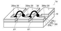
- FIG. 1is a main part diagram for explaining the thin film solar cell according to the present embodiment. That is, FIG. 1 is a perspective view of a main part of a thin film solar cell (solar cell module) 1a.
- the thin film solar cell 1amainly includes a substrate 10, a plurality of solar cells 20 formed on the substrate 10, and a metal wire 30 that electrically connects the solar cells 20 in series.
- Each of the solar cells 20has a transparent electrode layer 20a as a lower electrode, a photoelectric conversion layer 20b made of a thin film semiconductor material, and a metal electrode layer 20c laminated from the lower layer.
- Each solar battery cell 20is provided with a hole 20ha where the transparent electrode layer 20a is locally exposed.
- the transparent electrode layer 20 a at the bottom of the hole 20 ha and the metal electrode layer 20 c of the adjacent solar battery cell 20are electrically connected by a metal wire 30.
- the number of such photovoltaic cells 20is not limited to the number shown in the figure, and the number is adjusted according to the required output voltage. Then, by repeating the electrical connection described above, a necessary voltage is output between the upper electrode of the first solar cell in series connection and the lower electrode of the last solar cell in series connection.
- Each solar battery cell 20 separated by the groove tr1is formed by dividing the laminated body of the planar transparent electrode layer 20a, the photoelectric conversion layer 20b, and the metal electrode layer 20c at once by a method such as laser scribing. (Described later).
- the transparent electrode layer 20aAs a material of the substrate 10, for example, glass or an insulating resin film is applied.
- TCOTransparent Conductive Oxide
- ITOIndium Tin Oxide
- a silicon-based or compound-based semiconductor materialis applied as a material of the photoelectric conversion layer 20b.
- a silicon-based or compound-based semiconductor materialis applied as a material of the photoelectric conversion layer 20b.
- amorphous silicon, CIGS (Cu (InGa) Se 2 ) and the likeare typical examples.
- Such a photoelectric conversion layer 20bhas, for example, a structure in which a p-type and an n-type semiconductor layer are joined. When light is absorbed by the photoelectric conversion layer 20b, electric power (voltage) is generated between the transparent electrode layer 20a and the metal electrode layer 20c due to the photovoltaic effect.
- the metal electrode layer 20cAs a material of the metal electrode layer 20c, silver (Ag), aluminum (Al), zinc (Zn), or nickel (Ni) is applied.
- the film thickness of the transparent electrode layer 20ais, for example, about 1 ⁇ m
- the film thickness of the photoelectric conversion layer 20bis, for example, about 2 ⁇ m
- the film thickness of the metal electrode layer 20cis, for example, about 1 ⁇ m.
- the width of the trench tr1is, for example, 50 ⁇ m.
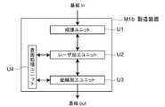
- FIG. 2is a main part diagram for explaining the configuration of the manufacturing apparatus. That is, FIG. 2 is a block diagram of the manufacturing apparatus M1a.
- FIGS. 3A to 6Bare principal views for explaining a method of manufacturing the thin-film solar cell 1a.
- the manufacturing apparatus M1aincludes a film forming unit U1, a laser processing unit U2, and a wiring processing unit U3.
- a film forming processis performed on the substrate 10 in a reduced pressure atmosphere.
- laser processing unit U2laser processing of the coating is performed in the atmosphere.
- wiring processing unit U3wiring for the series connection described above is performed.
- Each of these units U1 to U3can go back and forth. Further, by arranging these units U1 to U3 close to each other in a straight line, the size of the manufacturing apparatus M1a can be reduced. Further, the processing in each of the units U1 to U3 can be performed continuously.
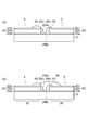
- the substrate 10is installed in the film forming unit U1 of the manufacturing apparatus M1a, and as shown in FIG. 3A, on the rectangular substrate 10, a planar (solid) transparent electrode layer 20a, photoelectric conversion is performed.
- the layer 20b and the metal electrode layer 20care formed by sputtering, PVD (Physical Vapor Deposition), CVD (Chemical Vapor Deposition), or the like.
- PVDPhysical Vapor Deposition
- CVDChemical Vapor Deposition
- a planar laminate 20lcomposed of the transparent electrode layer 20a, the photoelectric conversion layer 20b, and the metal electrode layer 20c is formed on the substrate 10.
- These transparent electrode layer 20a, photoelectric conversion layer 20b, and metal electrode layer 20care each formed without being exposed to the atmosphere.
- the laminate 20l and the substrate 10are moved to the laser processing unit U2, and laser scribe is applied to the laminate 20l as shown in FIG. Thereby, the laminate 20l on the substrate 10 is divided into strips having a predetermined width. That is, laser scribing is collectively performed on the transparent electrode layer 20a, the photoelectric conversion layer 20b, and the metal electrode layer 20c formed on the substrate 10 to form the groove tr1 in the portion irradiated with the laser.
- laser processing(laser scribing) is performed on at least one place of the photoelectric conversion layer 20b and the metal electrode layer 20c in each strip-shaped laminate 20l. Then, the photoelectric conversion layer 20b and the metal electrode layer 20c on the transparent electrode layer 20a are selectively removed in a spot shape. This state is shown in FIG. Thereby, the hole 20ha where the transparent electrode layer 20a is exposed is formed in each strip-shaped laminate 20l.
- the strip-shaped laminate 20l and the substrate 10are moved to the wiring processing unit U3, and the transparent electrode layer 20a exposed in the hole 20ha and the metal electrode layer 20c of the laminate 20l adjacent thereto are made into metal. Electrical connection is made through the wire 30.
- This stateis shown in FIG.
- the thin film solar cell 1a in which the plurality of solar cells 20 are provided on the substrate 10is formed.
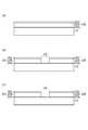
- FIG. 5shows an upper surface of the thin film solar cell 1a.
- each solar battery cell 20 of the thin-film solar battery 1 ais provided with a hole 20 ha where the transparent electrode layer 20 a is exposed.
- the transparent electrode layer 20 a exposed in the hole 20 ha of a certain solar battery cell 20 and the metal electrode layer 20 c of the solar battery cell 20 adjacent theretoare electrically connected through the metal wire 30.
- a necessary voltageis generated between the transparent electrode layer 20a of the first solar cell 20 in series connection and the metal electrode layer 20c of the last solar cell 20 in series connection. Is output.
- FIG. 5shows an example in which two holes 20 ha are provided for one solar battery cell 20. However, in this embodiment, it is not necessary to limit to this number. If necessary, the number of holes 20ha may be increased or decreased from two. Moreover, in FIG. 5, the example which has arrange
- the positions of the holes 20ha and the metal wires 30may be shifted every other.
- the freedom degree of the metal wire 30 joined to the metal electrode layer 20cincreases.
- the width of the solar battery cell 20the width in the direction substantially perpendicular to the groove tr1
- the degree of freedom of the joint portion of the metal wire 30increases. Therefore, in Fig.6 (a), the increase in the number of the photovoltaic cells 20 can be aimed at rather than the form shown in FIG.
- each solar battery cell 20as shown in FIG. 6B, a plurality of grooves tr ⁇ b> 2 that are substantially perpendicular to the groove tr ⁇ b> 1 are formed, and the strip-shaped solar battery cells 20 are arranged in the longitudinal direction. It may be divided into a plurality of grids. And the hole part 20hb for exposing the transparent electrode layer 20a may be formed substantially parallel with respect to the groove
- the electrical connection performed in the wiring processing unit U3may depend on connection means such as a conductive paste, a conductive paint, or a conductive tape in addition to the metal wire 30 described above.
- the laminated body 20l composed of the transparent electrode layer 20a, the photoelectric conversion layer 20b, and the metal electrode layer 20cis collectively laser-scribed, so that complicated positioning accuracy is not required. Moreover, since the number of manufacturing steps is reduced by the batch processing, the cost of the thin-film solar cell 1a and the manufacturing apparatus M1a is not increased.
- each solar battery cell 20is divided by one groove tr1, the area of a portion that does not contribute to power generation can be reduced (described later). Thereby, power generation efficiency improves.
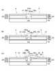
- FIG. 7is a main part diagram for explaining a comparative example of a thin film solar cell.
- a groove tra that penetrates to the substrate 10and a groove trb and a trc that penetrate to the transparent electrode layer 20a are formed.
- the transparent electrode layers 20aare separated from each other by the groove tra.
- a metal electrode layer 20cis embedded in the trench trb.
- adjacent photovoltaic cells 200are electrically connected in series.
- the vacuum opening for laser scribingis performed for the first time after forming the transparent electrode layer 20a and then forming the groove tra, and for the second time when forming the groove trb after forming the photoelectric conversion layer 20b.
- a total of three times of vacuum openingis required, that is, the third time when the groove trc is formed after the metal electrode layer 20c is formed.
- the frequency of reattachment of dust generated by splash or the like to each layer of the solar battery cell 200 during laser scribingis greater than when the solar battery cell 20 is formed.
- the thin film solar cell 100since it is necessary to execute laser scribing each time, complicated positioning accuracy is required in each laser scribing process.
- the laser scribing processis not batch processing, the number of manufacturing processes increases, resulting in high costs of the thin film solar cell and the manufacturing apparatus.
- each solar cell 200has a portion that does not contribute to power generation (portion A in the figure) remains. Accordingly, each cell width cannot be reduced.
- the length of the portion Ais in a direction substantially perpendicular to the groove tra, for example, 300 ⁇ m to 400 ⁇ m, and is wider than the groove tr1.
- the portion A shown in FIG. 7does not exist, and the solar cells 20 are provided on the substrate 10 with the groove tr1 therebetween.
- the present embodimenthas the advantageous effects as described above.
- the solar cells 20may be substantially square, and the arrangement of the solar cells 20 at that time may be a grid pattern. Further, the grooves tr1 do not need to be parallel to each other, and may be non-parallel as necessary. Further, the width and shape of each solar battery cell 20 need not be the same. In addition, there may be any number of electrical connection portions in each solar battery cell 20 in each solar battery cell 20. Moreover, in each photovoltaic cell 20, the position of the connection part may differ.
- the configuration of the solar battery cell 20is a three-layer structure, but a solar cell (tandem type, triple type) in which a multilayer film is formed can also be supported, and lamination at the time of laser scribing processing. There is no restriction on the number of layers of the film.
- FIG. 8A to FIG. 9Bare principal views for explaining a modification of the manufacturing process of the thin-film solar cell.
- the substrate 10is installed in the film forming unit U1 of the manufacturing apparatus M1a, and the planar transparent electrode layer 20a, the photoelectric conversion layer 20b, and the metal electrode layer 20c are formed on the substrate 10.
- a planar laminate 20lcomposed of the transparent electrode layer 20a, the photoelectric conversion layer 20b, and the metal electrode layer 20c is formed on the substrate 10.
- the laminate 20lis formed by a PVD method or a CVD method.
- the laminate 20l and the substrate 10are moved to the laser processing unit U2, and laser scribe is applied to the laminate 20l as shown in FIG. 8 (b).
- the photoelectric conversion layer 20b and the metal electrode layer 20care divided into a predetermined width in the stacked body 20l. That is, the trench tr3 that divides the photoelectric conversion layer 20b and the metal electrode layer 20c at a predetermined interval is formed. Thereby, a part of surface of the transparent electrode layer 20a is exposed.
- laser scribeis applied to a part of the transparent electrode layer 20a exposed in the groove tr3, and the exposed part of the transparent electrode layer 20a is divided into a predetermined width. As a result, a part of the surface of the substrate 10 is exposed.
- the process shown in FIG. 8Cis collectively performed by continuously switching the laser wavelength when processing the photoelectric conversion layer 20b and the metal electrode layer 20c and the laser wavelength when processing the transparent electrode layer 20a. It may be processed.
- the laminate 20l in which the groove tr3 is formed and the substrate 10are moved to the wiring processing unit U3, and as shown in FIG. 9A, a part of the transparent electrode layer 20a exposed in the groove tr3 is removed.
- the insulating member 40selectively covers the vicinity of the side surface 20lw and the corner portion 20lc on both sides of the groove tr3 while being exposed.
- a part of the transparent electrode layer 20a, the side surface 20lw, and the vicinity of the corner 20lc shown in the drawing by the arrow aare covered with the insulating member 40.
- the insulating member 40covers the vicinity of the side surface 20lw and the corner portion 20lc of the laminate 20l indicated by the arrow b in the figure.
- Such covering of the insulating member 40is performed by, for example, any one of an inkjet coating method, a dispense coating method, a transfer method, and a printing method. Moreover, if such a process is followed, the covering of the insulating member 40 will be quick and low cost.
- the material of the insulating member 40corresponds to an inorganic material paste, an organic resin, an organic paint, or the like. In the case of an organic resin, it may be in the form of a tape.
- the metal electrode layer of the laminate 20l indicated by the arrow bfrom the gap between the laminate 20l indicated by the arrow a and the insulating member 40 formed in the laminate 20l indicated by the arrow b.
- the conductive connection member 50is formed so as to continue to the surface of 20c, and the transparent electrode layer 20a of the laminate 20l indicated by the arrow a is electrically connected to the metal electrode layer 20c of the laminate 20l indicated by the arrow b.
- the formation of the conductive connection member 50is performed by any one of, for example, an ink jet coating method, a dispense coating method, a transfer method, a printing method, and a pasting method. Moreover, according to such a process, the conductive connection member 50 can be formed quickly and at low cost.
- the material of the conductive connection member 50corresponds to conductive paste, conductive paint, low-temperature solder, nano silver fine particles, carbon nanotubes, nano silver fine particle-containing conductive paste, carbon nanotube-containing conductive paste, conductive film, and the like. To do.
- the solar battery cell 20(first solar battery cell) indicated by the arrow a and the solar battery cell 20 (second solar battery cell) indicated by the arrow b formed on the substrate 10 are formed. Connected in series.
- Example 2the same effect as in Example 1 can be obtained because the vacuum is released only once.
- the insulating member 40 and the conductive connection member 50are formed by any one of the ink jet coating method, the dispense coating method, the transfer method, and the printing method. become. Thereby, the productivity of the thin film solar cell is further improved.
- Example 3Next, still another modification of the manufacturing process of the thin film solar cell using the thin film solar cell manufacturing apparatus will be described.
- the laser scribing process of the laminate 20lis the same as that in FIG. 8, and will be described from the next step.
- FIGS. 10 (a) to 10 (c)are principal part views for explaining another modified example of the manufacturing process of the thin-film solar cell.
- the laminate 20l formed with the groove tr3 and the substrate 10are moved to the wiring processing unit U3, and the insulating member 40 is embedded in the groove tr3 as shown in FIG.
- the burying of the insulating member 40is performed by, for example, any one of an ink jet coating method, a dispense coating method, a transfer method, and a printing method. If such a process is followed, the covering of the insulating member 40 is quick and low cost.
- the material of the insulating member 40corresponds to an inorganic material paste, an organic resin, an organic paint, or the like.
- angular part 20lc vicinity of the laminated body 20l shown by the arrow aare coat
- the insulating member 40covers the vicinity of the side surface 20lw and the corner portion 20lc of the laminate 20l indicated by the arrow b.
- the laminate 20l and the substrate 10are moved again to the laser processing unit U2, and the insulating member 40 is subjected to laser scribing as shown in FIG.
- a groove tr4is formed in the central portion of the insulating member 40, and the transparent electrode layer 20a of the laminate 20l indicated by the arrow a in the drawing is exposed. Since the groove tr4 is formed only in the central portion of the insulating member 40, a part of the transparent electrode layer 20a, the side surface 20lw and the corner portion 20lc in the vicinity of the laminated body 20l indicated by arrows a and b in the figure are insulated members. 40.
- the laminate 20l and the substrate 10are moved again to the wiring processing unit U3, and, as shown in FIG. 10C, continue from the trench tr4 to the surface of the metal electrode layer 20c of the laminate 20l indicated by the arrow b.
- the conductive connection member 50is formed. Thereby, the transparent electrode layer 20a of the laminate 20l indicated by the arrow a and the metal electrode layer 20c of the laminate 20l indicated by the arrow b are electrically connected.
- the formation of the conductive connection member 50is performed by any one of, for example, an ink jet coating method, a dispense coating method, a transfer method, a printing method, and a pasting method. If such a process is followed, formation of the conductive connection member 50 is quick and low cost.
- the material of the conductive connection member 50corresponds to conductive paste, conductive paint, low-temperature solder, nano silver fine particles, carbon nanotube, nano silver fine particle-containing conductive paste, carbon nanotube-containing conductive paste, conductive film, and the like. To do.
- the solar battery cell 20 indicated by the arrow a and the solar battery cell 20 indicated by the arrow b formed on the substrate 10are connected in series.
- Example 3the same effect as in Example 1 can be obtained because the vacuum is released only once.
- the insulating member 40 and the conductive connection member 50are formed by any one of the ink jet coating method, the dispense coating method, the transfer method, and the printing method, wiring processing is quick and low cost. become. Thereby, the productivity of the thin film solar cell is further improved.
- Example 4Next, still another modification of the manufacturing process of the thin film solar cell using the thin film solar cell manufacturing apparatus will be described.
- the laser scribing process of the laminate 20lis the same as in FIG. 8, and will be described from the next step.
- FIGS. 11 (a) to 11 (c)are principal part views for explaining still another modified example of the manufacturing process of the thin film solar cell.
- the laminate 20l formed with the groove tr3 and the substrate 10are moved to the wiring processing unit U3, and a planar insulating member 41 is formed in the trench tr3 and on the laminate 20l as shown in FIG. To do.
- the insulating member 41is formed by any one of an ink jet coating method, a dispense coating method, a transfer method, a printing method, and a pasting method, for example. Moreover, if such a process is followed, formation of the insulating member 41 will be quick and low cost.
- the material of the insulating member 41corresponds to a resin film, an organic resin, an organic paint, an inorganic material paste, or the like.
- angular part 20lc vicinity of the laminated body 20l shown by the arrow a in a figureare coat
- the insulating member 41covers the vicinity of the side surface 20lw and the corner portion 20lc of the laminate 20l indicated by the arrow b in the drawing.
- the laminate 20l and the substrate 10are moved again to the laser processing unit U2, and laser scribing is performed at two locations on the insulating member 41 as shown in FIG.
- the groove tr4is formed at the center of the insulating member 41 formed in the groove tr3, and the transparent electrode layer 20a of the laminate 20l indicated by the arrow a is exposed.
- the groove tr5is also formed in the insulating member 41 on the stacked body 20l indicated by the arrow b, and the metal electrode layer 20c is exposed.
- the groove tr4is formed only in the central part of the insulating member 41 formed in the groove tr3, a part of the transparent electrode layer 20a, the side surface 20lw, and the corner part 20lc in the vicinity of the laminated body 20l indicated by the arrow a are insulated. Covered with a member 41. Further, the vicinity of the side surface 20lw and the corner portion 20lc of the laminate 20l indicated by the arrow b is covered with an insulating member 41.
- the laminate 20l and the substrate 10are moved again to the wiring processing unit U3, and the conductive connection member 50 is formed so as to be continuous from the groove tr4 to the groove tr5 as shown in FIG. 11C. .
- the transparent electrode layer 20a of the laminate 20l indicated by the arrow a and the metal electrode layer 20c of the laminate 20l indicated by the arrow bare electrically connected.
- the formation of the conductive connection member 50is performed by any one of, for example, an ink jet coating method, a dispense coating method, a transfer method, a printing method, and a pasting method. If such a process is followed, formation of the conductive connection member 50 is quick and low cost.
- the material of the conductive connection member 50corresponds to conductive paste, conductive paint, low-temperature solder, nano silver fine particles, carbon nanotubes, nano silver fine particle-containing conductive paste, carbon nanotube-containing conductive paste, conductive film, and the like. To do.
- the solar battery cell 20 indicated by the arrow a and the solar battery cell 20 indicated by the arrow b formed on the substrate 10are connected in series.
- Example 4the same effect as in Example 1 can be obtained because the vacuum is released only once.
- the insulating member 41 and the conductive connection member 50are formed by any one of the inkjet coating method, the dispense coating method, the transfer method, the printing method, and the pasting method, the wiring processing is performed. Done quickly and at low cost. Since the insulating member 41 serves as a protective layer for the laminate 20l, the reliability of the battery is enhanced. In addition, a separate step of providing a protective film becomes unnecessary. Thereby, the productivity of the thin film solar cell is further improved.
- Example 5Next, still another modification of the manufacturing process of the thin film solar cell using the thin film solar cell manufacturing apparatus will be described.
- the laser scribing process of the laminate 20lis the same as that in FIG. 8, and will be described from the next step.
- 12 (a) to 12 (c)are principal part views for explaining still another modified example of the manufacturing process of the thin film solar cell.
- the laminate 20l formed with the groove tr3 and the substrate 10are moved to the wiring processing unit U3, and as shown in FIG. 12A, a part of the transparent electrode layer 20a formed in the groove tr3 and the arrow b
- a water repellent member 60is formed on a part of the metal electrode layer 20c of the laminate 20l shown in FIG. That is, a water repellent treatment is performed on these portions.
- the water repellent member 60corresponds to, for example, a chemical for water repellent processing.
- the water repellent treatmentmay be performed by selectively performing laser treatment, plasma treatment (formation of surface water repellent groups), or the like on this portion in addition to forming the above-described water repellent member 60.
- a planar insulating member 41is formed.
- the insulating member 41is formed by any one of an ink jet coating method, a dispense coating method, a transfer method, and a printing method, for example.
- a part of the transparent electrode layer 20a formed in the groove tr3 and a part of the metal electrode layer 20c of the laminated body 20l indicated by the arrow bare subjected to water repellent processing. Accordingly, the adhesion of the insulating member 41 to these portions is suppressed, and as shown in the figure, a groove tr4 is generated at the center of the insulating member 41 formed in the groove tr3, and the transparent body 20l indicated by the arrow a is transparent.
- the insulating member 41is formed in addition to the portion where the transparent electrode layer 20a and the metal electrode layer 20c are electrically connected.
- the material of the insulating member 41corresponds to an organic resin, an organic paint, an inorganic material paste, or the like.
- the trench tr4is generated only in the central portion of the insulating member 41 formed in the trench tr3, a part of the transparent electrode layer 20a, the side surface 20lw, and the vicinity of the corner portion 20lc indicated by the arrow a are insulated. Covered with a member 41. Further, the vicinity of the side surface 20lw and the corner portion 20lc of the laminate 20l indicated by the arrow b is covered with an insulating member 41.
- the electroconductive connection member 50is formed so that it may continue in the groove
- the transparent electrode layer 20a of the laminate 20l indicated by the arrow a and the metal electrode layer 20c of the laminate 20l indicated by the arrow bare electrically connected.
- the formation of the conductive connection member 50is performed by any one of, for example, an ink jet coating method, a dispense coating method, a transfer method, a printing method, and a pasting method. Moreover, if such a process is followed, formation of the conductive connection member 50 is quick and low cost.
- the material of the conductive connection member 50corresponds to conductive paste, conductive paint, low-temperature solder, nano silver fine particles, carbon nanotubes, nano silver fine particle-containing conductive paste, carbon nanotube-containing conductive paste, conductive film, and the like. To do.
- the solar battery cell 20 indicated by the arrow a and the solar battery cell 20 indicated by the arrow b formed on the substrate 10are connected in series.
- the same effect as that of the first embodimentcan be obtained because the vacuum is released only once.
- the formation of the insulating member 41 and the conductive connection member 50is performed by any one of the inkjet coating method, the dispense coating method, the transfer method, the printing method, and the pasting method, the wiring processing is performed. Quick and low cost.
- the productivityis higher. Thereby, the productivity of the thin film solar cell is further improved.
- FIG. 13A and FIG. 13Bare main part views for explaining still another modified example of the manufacturing process of the thin film solar cell.
- the stacked body 20l and the substrate 10are moved to the laser processing unit U2. Then, as shown in FIG. 13A, laser scribing is performed from above the stacked body 20l. Thereby, the stacked body 20l is divided across the groove tr3. However, in Example 6, a step is formed between the photoelectric conversion layer 20b and the metal electrode layer 20c between the transparent electrode layer 20a and the photoelectric conversion layer 20b of the laminate 20l indicated by arrows a and b. Is subjected to laser processing.
- the side surface 20cw of the metal electrode layer 20crecedes from the side surface 20bw of the photoelectric conversion layer 20b on the side surface of the divided laminate 20l. Further, for example, the side surface 20bw of the photoelectric conversion layer 20b is set back relative to the side surface 20aw of the transparent electrode layer 20a.
- the creeping distance of the photoelectric conversion layer 20b exposed on the side surface of the laminate 20lcan be increased, and leakage between the transparent electrode layer 20a and the metal electrode layer 20c can be suppressed.
- the photoelectric conversion layer 20bis laser processed after the metal electrode layer 20c is processed, the distance between the side surface 20cw of the metal electrode layer 20c and the side surface 20bw of the photoelectric conversion layer 20b is increased. Therefore, when laser scribing the photoelectric conversion layer 20b, leakage due to thermal alteration on the side surface of the stacked body 20l is suppressed.
- the insulating member 40 and the conductive connection member 50are formed, and the transparent electrode layer 20a of the laminate 20l indicated by the arrow a and the metal electrode of the laminate 20l indicated by the arrow b.
- the layer 20cis electrically connected. This state is shown in FIG. Through such a process, the solar battery cell 20 indicated by the arrow a and the solar battery cell 20 indicated by the arrow b formed on the substrate 10 are connected in series.
- Example 6the same effect as in Example 1 can be obtained because the vacuum is released only once.
- the reattachment of splash to the side surface 20lw of the laminate 20lis suppressed, and a high-quality thin-film solar cell is formed.
- FIG. 14A and FIG. 14Bare main part views for explaining still another modified example of the manufacturing process of the thin film solar cell.
- the arrowAs shown to Fig.14 (a), on the board
- FIG. 15A and FIG. 15Bare main part views for explaining still another modified example of the manufacturing process of the thin film solar cell.
- the arrowAs shown to Fig.15 (a), on the board
- the conductive connection member 50is embedded in the groove tr3 (groove tr3 formed by dividing the laminated film 20l).
- the conductive connection member 50is removed by laser scribing from the side surfaces of the metal electrode layer 20c and the photoelectric conversion layer 20b of the solar battery cell indicated by the arrow a, and the transparent electrode exposed.
- a trench tr6is formed on the layer 20a.
- a hydrophilization treatmentis performed on the portion where the metal wire 30 and the conductive connection member 50 are joined in order to improve the wettability (adhesion) of these conductive materials. Also good.
- plasma treatment, ultrasonic treatment, chemical application, washing with water, etc.may be performed to perform hydrophilic treatment on the joint portion.
- the direction in which the laser light is incidentmay be the direction from the metal electrode layer 20c of the stacked body 20l to the transparent electrode layer 20a, and from the transparent electrode layer 20a.
- the direction of the metal electrode layer 20cmay also be used.
- the incidence of laser lightincludes normal incidence and oblique incidence on the substrate 10.
- the above-described laser scribing processmay be performed by leaning the substrate 10 and the laminated film 20l against the ground.
- FIG. 16is a main part diagram for explaining a modification of the thin-film solar cell according to the present embodiment.
- the manufacturing apparatus M1bincludes a film forming unit U1, a laser processing unit U2, a wiring processing unit U3, and a surface treatment unit U4.
- a surface treatment unit U4By incorporating such a surface treatment unit U4 into the manufacturing apparatus M1b, the above-described surface treatment can be performed.
- the surface treatment unit U4in addition to the cleaning treatment, the water repellent treatment and the hydrophilic treatment described above can be performed together.
- surface treatmentis performed on at least a part of the groove formed by dividing the laminated film 20l or at least a part of each surface of the plurality of solar cells 20, Surface modification of the part is performed.
- the insulating member 41can respond, even if the material of the insulating member 41 is hydrophilic or water-repellent.
- the insulating member 41is formed in addition to the portion where the conductive connecting member 50 is joined to the transparent electrode layer 20a and the metal electrode layer 20c.
- the water-repellent member 60is selectively formed in the part which joins the electroconductive connection member 50 to the transparent electrode layer 20a and the metal electrode layer 20c, ie, the part which does not arrange
- the hydrophilic insulating member 41when the hydrophilic insulating member 41 is used, a hydrophilic treatment may be selectively performed on a base on which the insulating member 41 is formed. In the case where the water-repellent insulating member 41 is used, the portion where the insulating member 41 is not formed may be selectively subjected to water repellent treatment.
- the material of the metal wire 30 and the electroconductive connection member 50is hydrophilic, it can respond.
- a hydrophilization treatmentmay be performed on a base on which the metal wire 30 and the conductive connection member 50 are bonded.
- the water repellent treatmentmay be performed on a portion other than the base to which the metal wire 30 and the conductive connection member 50 are joined.
Landscapes
- Photovoltaic Devices (AREA)
Abstract
Description
Translated fromJapanese本発明は、太陽電池の製造方法、太陽電池の製造装置及び太陽電池に関する。The present invention relates to a solar cell manufacturing method, a solar cell manufacturing apparatus, and a solar cell.
近年、環境保護の立場から、クリーンなエネルギーの研究開発が進められている。中でも、太陽電池は資源となる太陽光が無限であること、無公害であることから注目を集めている。
同一基板上に形成された複数の太陽電池セルが、直列接続された太陽電池(光電変換装置)の代表例は、薄膜太陽電池である。
薄膜太陽電池は、薄型で軽量、製造コストの安さ、大面積化が容易であることから、今後の太陽電池の主流となると考えられている。また、薄膜太陽電池は、電力供給用以外に、建物の屋根や窓などにとりつけて利用される業務用、一般住宅用にも需要が広がってきている。In recent years, research and development of clean energy has been promoted from the standpoint of environmental protection. Above all, solar cells are attracting attention because of the infinite amount of sunlight that is a resource and no pollution.
A typical example of a solar cell (photoelectric conversion device) in which a plurality of solar cells formed on the same substrate are connected in series is a thin film solar cell.
Thin film solar cells are considered to become the mainstream of future solar cells because they are thin and lightweight, inexpensive to manufacture, and easy to increase in area. In addition to power supply, thin-film solar cells are also in demand for business use and general residential use that are attached to the roofs and windows of buildings.
従来の薄膜太陽電池は、ガラス基板を用いているものが一般的であった。このような薄膜太陽電池は、ガラス基板上に、その下層から下部電極、半導体層からなる光電変換層、上部電極が積層された光電変換素子(またはセル)が複数形成されている。そして、任意の光電変換素子の上部電極と、これに隣接する光電変換素子の下部電極とを電気的に接続する構成が繰り返されている。これにより、最初の光電変換素子の上部電極と最後の光電変換素子の下部電極との間に必要な電圧が出力される。Conventional thin film solar cells generally use a glass substrate. In such a thin film solar cell, a plurality of photoelectric conversion elements (or cells) in which a lower electrode, a photoelectric conversion layer made of a semiconductor layer, and an upper electrode are stacked are formed on a glass substrate. And the structure which electrically connects the upper electrode of arbitrary photoelectric conversion elements and the lower electrode of the photoelectric conversion element adjacent to this is repeated. Thereby, a necessary voltage is output between the upper electrode of the first photoelectric conversion element and the lower electrode of the last photoelectric conversion element.
このような光電変換素子間の直列接続は、電極層と光電変換層の成膜と各層のパターニング、およびこれらの組み合わせによりなされる。そして、最近では、基板上に積層された膜をレーザ加工により分断して、光電変換素子を直列接続する方法が開示されている(例えば、特許文献1参照)。Such series connection between the photoelectric conversion elements is performed by forming an electrode layer and a photoelectric conversion layer, patterning each layer, and a combination thereof. Recently, a method has been disclosed in which a film laminated on a substrate is divided by laser processing to connect photoelectric conversion elements in series (for example, see Patent Document 1).
しかしながら、上述した方法は、直列接続するための配線工程や製造工程中での位置合わせが複雑になり、簡便な方法で太陽電池を製造したものではない。However, in the above-described method, the alignment in the wiring process and the manufacturing process for connecting in series is complicated, and the solar cell is not manufactured by a simple method.
本発明は、上述した直列接続を簡略化することにより、太陽電池及びそれを製造する製造装置の低コスト化を図ると共に、太陽電池の品質を向上し、太陽電池の発電効率が向上する太陽電池の製造方法、太陽電池の製造装置及び太陽電池を提供することを目的とする。The present invention simplifies the series connection described above, thereby reducing the cost of the solar cell and the manufacturing apparatus for manufacturing the solar cell, improving the quality of the solar cell, and improving the power generation efficiency of the solar cell. An object of the present invention is to provide a manufacturing method, a solar cell manufacturing apparatus, and a solar cell.
本発明の一態様によれば、基板上に、複数の太陽電池セルが直列に接続された太陽電池の製造方法であって、前記基板上に、第1の電極膜を減圧雰囲気下で形成し、その後、大気に曝すことなく、前記第1の電極膜上に、光電変換層を減圧雰囲気下で形成し、その後大気に曝すことなく、前記光電変換層上に、第2の電極膜を減圧雰囲気下で形成して、積層膜を形成する工程と、前記積層膜を分断して、前記基板上に併設された前記複数の太陽電池セルを形成する工程と、前記複数の太陽電池セルのうちの第1の太陽電池セルの前記第2の電極膜及び前記光電変換層を選択的に除去して、前記第1の電極膜を表出させ、前記第1の太陽電池セルに隣接する第2の太陽電池セルの前記第2の金属膜と、表出させた前記第1の電極膜と、を電気的に接続する工程と、を備えたことを特徴とする太陽電池の製造方法が提供される。According to one aspect of the present invention, there is provided a solar cell manufacturing method in which a plurality of solar cells are connected in series on a substrate, wherein the first electrode film is formed on the substrate in a reduced-pressure atmosphere. Thereafter, the photoelectric conversion layer is formed on the first electrode film in a reduced pressure atmosphere without exposure to the air, and then the second electrode film is reduced on the photoelectric conversion layer without exposure to the air. Of the plurality of solar cells, a step of forming a laminated film by forming in an atmosphere, a step of dividing the laminated film to form the plurality of solar cells arranged on the substrate, and The second electrode film and the photoelectric conversion layer of the first solar cell are selectively removed to expose the first electrode film, and the second solar cell adjacent to the first solar cell. The second metal film of the solar battery cell and the exposed first electrode film are electrically connected Method of manufacturing a solar cell characterized by comprising the steps, a to be connected are provided.
また、本発明の一態様によれば、基板上に、複数の太陽電池セルが直列に接続された太陽電池の製造装置であって、前記基板上に、第1の電極膜を減圧雰囲気下で形成し、その後、大気に曝すことなく、前記第1の電極膜上に、光電変換層を減圧雰囲気下で形成し、その後大気に曝すことなく、前記光電変換層上に、第2の電極膜を減圧雰囲気下で形成して、積層膜を形成する第1の手段と、前記積層膜を分断して、前記基板上に併設された前記複数の太陽電池セルを形成する第2の手段と、前記併設された前記複数の太陽電池セルのうちの前記第1の太陽電池セルの前記第2の電極膜及び前記光電変換層を選択的に除去して、前記第1の電極膜を表出させ、前記第2の太陽電池セルの前記第2の金属膜と、表出させた前記第1の電極膜と、を接続する第3の手段と、を備えたことを特徴とする太陽電池の製造装置が提供される。According to another aspect of the present invention, there is provided a solar cell manufacturing apparatus in which a plurality of solar cells are connected in series on a substrate, wherein the first electrode film is placed on the substrate in a reduced-pressure atmosphere. Forming a photoelectric conversion layer on the first electrode film in a reduced-pressure atmosphere without exposing to the air, and then exposing the second electrode film on the photoelectric conversion layer without exposing to the air. A first means for forming a laminated film, and a second means for dividing the laminated film to form the plurality of solar cells provided on the substrate; The first electrode film is exposed by selectively removing the second electrode film and the photoelectric conversion layer of the first solar battery cell among the plurality of solar battery cells provided side by side. The second metal film of the second solar cell, and the exposed first electrode film, Third means for connecting, the apparatus for manufacturing a solar cell comprising the is provide.
また、本発明の一態様によれば、基板上に形成された、第1の電極膜と、前記第1の電極膜の上に設けられた光電変換層と、前記光電変換層の上に設けられた第2の電極膜と、を含む積層膜が一括して分断されて前記基板上に併設された複数の太陽電池セルと、前記複数の太陽電池セルを直列に接続する接続部材と、を備えたことを特徴とする太陽電池が提供される。According to one embodiment of the present invention, a first electrode film formed on a substrate, a photoelectric conversion layer provided on the first electrode film, and provided on the photoelectric conversion layer A plurality of solar cells provided on the substrate by dividing a laminated film including the second electrode film, and a connecting member for connecting the plurality of solar cells in series. There is provided a solar cell comprising the above.
本発明によれば、太陽電池及びそれを製造する製造装置の低コスト化がなされ、太陽電池の品質が向上し、太陽電池の発電効率が向上する。According to the present invention, the cost of the solar cell and the manufacturing apparatus for manufacturing the solar cell is reduced, the quality of the solar cell is improved, and the power generation efficiency of the solar cell is improved.
以下、図面を参照しつつ、本発明の実施の形態について説明する。Hereinafter, embodiments of the present invention will be described with reference to the drawings.
(実施例1)
図1は、本実施の形態に係る薄膜太陽電池を説明する要部図である。すなわち、図1は、薄膜太陽電池(太陽電池モジュール)1aの要部斜視図である。
薄膜太陽電池1aは、主に、基板10と、基板10に複数形成された太陽電池セル20と、それぞれの太陽電池セル20を電気的に直列状に接続する金属ワイヤ30と、を含む。Example 1
FIG. 1 is a main part diagram for explaining the thin film solar cell according to the present embodiment. That is, FIG. 1 is a perspective view of a main part of a thin film solar cell (solar cell module) 1a.
The thin film
それぞれの太陽電池セル20は、その下層から、下部電極としての透明電極層20a、薄膜半導体材からなる光電変換層20b、金属電極層20cが積層されている。それぞれの太陽電池セル20には、局部的に透明電極層20aが表出した孔部20haが設けられている。そして、孔部20haの底における透明電極層20aと、隣接する太陽電池セル20の金属電極層20cとが、金属ワイヤ30により電気的に接続されている。Each of the
なお、このような太陽電池セル20は、図示する個数に限らず、必要とされる出力電圧に応じて、その数が調節される。そして、上述した電気的な接続を繰り返すことにより、直列接続の最初の太陽電池セルの上部電極と、直列接続の最後の太陽電池セルの下部電極と、の間で必要な電圧が出力される。In addition, the number of such
なお、溝tr1を隔てた、それぞれの太陽電池セル20は、平面状の透明電極層20a、光電変換層20b及び金属電極層20cの積層体を一括でレーザスクライブなどの方法で分断することにより形成する(後述)。Each
基板10の材質としては、例えば、ガラス、絶縁性樹脂フィルムが適用される。
また、透明電極層20aとしては、いわゆるTCO(Transparent Conductive Oxide)等が適用される。その代表的なものとして、ITO(Indium Tin Oxide)が挙げられる。As a material of the
As the
また、光電変換層20bの材質としては、シリコン系、化合物系の半導体材が適用される。例えば、その代表的なものとして、アモルファスシリコン、CIGS(Cu(InGa)Se2)等が挙げられる。このような光電変換層20bは、例えば、p型とn型の半導体層が接合した構造を有している。そして、光電変換層20bに光が吸収されると、光起電力効果により透明電極層20a-金属電極層20c間に電力(電圧)が発生する。In addition, as a material of the
金属電極層20cの材質としては、銀(Ag)、アルミニウム(Al)、亜鉛(Zn)、ニッケル(Ni)が適用される。
透明電極層20aの膜厚は、例えば1μm程度であり、光電変換層20bの膜厚は、例えば2μm程度であり、金属電極層20cの膜厚は、例えば1μm程度である。
太陽電池セル20については、基本的な3層構造を例示したが、本実施の形態については、3層以上の構成であっても対応可能である。
また、溝tr1の幅は、例えば、50μmである。As a material of the
The film thickness of the
Although the basic three-layer structure is illustrated for the
The width of the trench tr1 is, for example, 50 μm.
次に、薄膜太陽電池製造装置(以下、製造装置)を用いて、薄膜太陽電池1aを製造する工程について説明する。
図2は、製造装置の構成を説明するための要部図である。すなわち、図2は、製造装置M1aのブロック図である。また、図3(a)~図6(b)は、薄膜太陽電池1aの製造方法を説明するための要部図である。Next, the process of manufacturing the thin film
FIG. 2 is a main part diagram for explaining the configuration of the manufacturing apparatus. That is, FIG. 2 is a block diagram of the manufacturing apparatus M1a. FIGS. 3A to 6B are principal views for explaining a method of manufacturing the thin-film
図2に示すように、製造装置M1aは、成膜ユニットU1と、レーザ加工ユニットU2と、配線加工ユニットU3と、を含む。成膜ユニットU1では、減圧雰囲気で基板10に成膜処理が行われる。レーザ加工ユニットU2では、大気中で被膜のレーザ加工が行われる。配線加工ユニットU3では、上述した直列接続のための配線が行われる。これらの各ユニットU1~U3間は、相互に行き来することができる。また、これらの各ユニットU1~U3を直線状に近接して配列することにより、製造装置M1aの小型化が実現できる。また、各ユニットU1~U3内での処理を連続して行うことができる。As shown in FIG. 2, the manufacturing apparatus M1a includes a film forming unit U1, a laser processing unit U2, and a wiring processing unit U3. In the film forming unit U1, a film forming process is performed on the
次に、上述した製造装置M1aを用いて薄膜太陽電池1aを製造する方法を具体的に説明する。
まず、基板10を製造装置M1aの成膜ユニットU1内に設置し、図3(a)に示すように、矩形状の基板10上に、平面状(べた状)の透明電極層20a、光電変換層20b及び金属電極層20cをスパッタリング法、PVD(Physical Vapor Deposition)法あるいはCVD(Chemical Vapor Deposition)法などにより形成する。これにより、基板10上に、透明電極層20a、光電変換層20b及び金属電極層20cで構成される、平面状の積層体20lが形成される。これらの透明電極層20a、光電変換層20b及び金属電極層20cは、それぞれ大気に晒されることなく形成される。Next, a method for manufacturing the thin-film
First, the
次に、積層体20l及び基板10をレーザ加工ユニットU2に移動して、図3(b)に示すように、積層体20lにレーザスクライブを施す。これにより、基板10上の積層体20lが所定の幅に短冊状に分断される。
すなわち、基板10上に形成された、透明電極層20a、光電変換層20b及び金属電極層20cに一括でレーザスクライブ加工を施して、レーザを照射した部分に溝tr1を形成する。Next, the laminate 20l and the
That is, laser scribing is collectively performed on the
さらに、それぞれの短冊状の積層体20lにおける、光電変換層20b及び金属電極層20cの少なくとも1箇所にレーザ加工(レーザスクライブ)を施す。そして、透明電極層20a上の光電変換層20b及び金属電極層20cを選択的にスポット状に除去する。この状態を、図4(a)に示す。これにより、それぞれの短冊状の積層体20lに、透明電極層20aが露出された孔部20haが形成される。Further, laser processing (laser scribing) is performed on at least one place of the
次に、短冊状の積層体20l及び基板10を配線加工ユニットU3に移動し、孔部20haにおいて露出している透明電極層20aと、これに隣接する積層体20lの金属電極層20cとを金属ワイヤ30を通じて電気的に接続する。この状態を、図4(b)に示す。このような工程により、基板10上に複数の太陽電池セル20が設けられた薄膜太陽電池1aが形成される。Next, the strip-shaped laminate 20l and the
図5には、薄膜太陽電池1aの上面が示されている。
図5に示すように、薄膜太陽電池1aの各太陽電池セル20の少なくとも一箇所には、透明電極層20aが表出した孔部20haが設けられている。そして、ある太陽電池セル20の孔部20haにおいて露出した透明電極層20aと、これに隣接する太陽電池セル20の金属電極層20cと、が金属ワイヤ30を通じて電気的に接続されている。このような電気的な接続の繰り返しによって、直列接続の最初の太陽電池セル20の透明電極層20aと、直列接続の最後の太陽電池セル20の金属電極層20cとの間に、必要な電圧が出力される。FIG. 5 shows an upper surface of the thin film
As shown in FIG. 5, at least one portion of each
なお、図5では、1個の太陽電池セル20に対し、2個の孔部20haを設けた例を示している。しかし、本実施の形態では、この数に限定する必要はない。必要に応じて、孔部20haの数を2個より増減してもよい。
また、図5においては、隣接する孔部20ha及び金属ワイヤ30を直線状に配置した例を示した。しかし、本実施の形態では、その配置に限定する必要はない。FIG. 5 shows an example in which two
Moreover, in FIG. 5, the example which has arrange | positioned the adjacent hole part 20ha and the
例えば、図6(a)に示すように、1個おきに孔部20ha及び金属ワイヤ30の位置をずらして配置してもよい。これにより、金属電極層20cに接合する金属ワイヤ30の自由度が増加する。また、図5に示す形態よりも、太陽電池セル20の幅(溝tr1に対し略垂直方向の幅)をより狭くしても、金属ワイヤ30の接合部分の自由度が増す。従って、図6(a)では、図5に示す形態よりも、太陽電池セル20の数の増加を図ることができる。For example, as shown in FIG. 6A, the positions of the holes 20ha and the
また、それぞれの太陽電池セル20においては、図6(b)に示すように、溝tr1に対し略垂直となる溝tr2を複数個形成して、短冊状の太陽電池セル20を、その長手方向に複数に分断し格子状としてもよい。そして、透明電極層20aを露出するための孔部20hbを溝tr2に対し略平行に形成して、格子状に分断した太陽電池セル20同士を金属ワイヤ30により直列状に接続してもよい。このような構成によれば、薄膜太陽電池1aの発電単位がさらに小さくなる。これにより、所望の出力電圧に応じて、チップ状の太陽電池セルの数を自由に選択することができる。すなわち、チップ状の太陽電池セルの個数を適宜変更して、それらを直列状に接続することにより、出力電圧の異なる薄膜太陽電池を容易に形成することができる。
なお、配線加工ユニットU3で行われる電気的な接続は、上述した金属ワイヤ30の他、導電性ペースト、導電性塗料、導電性テープ等の接続手段に依ってもよい。Further, in each
The electrical connection performed in the wiring processing unit U3 may depend on connection means such as a conductive paste, a conductive paint, or a conductive tape in addition to the
このように、本実施の形態では、積層体20lを予め形成した後、一括で積層体20lのレーザスクライブを行っている。このような方法では、薄膜太陽電池1aを製造する際、真空開放は、レーザスクライブを行う1回のみで足りる。また、この1回のみのレーザスクライブは、積層体20lが上述した3層よりも、さらに多層となっても実現可能である。As described above, in this embodiment, after the laminate 20l is formed in advance, laser scribe of the laminate 20l is performed in a lump. In such a method, when manufacturing the thin film
その結果、各層においては、各層の成膜とパターニング(レーザスクライブ)とを交互に繰り返さないので、レーザスクライブの際にスプラッシュ等で発生するゴミの太陽電池セル20への再付着が最小限に抑制される。その結果、薄膜太陽電池1aの製品歩留まりが向上する。As a result, in each layer, film formation and patterning (laser scribing) of each layer are not repeated alternately, so that the reattachment of dust generated by splash or the like during laser scribing to the
また、レーザスクライブにおいては、透明電極層20a、光電変換層20b及び金属電極層20cで構成される積層体20lを一括でレーザスクライブすることから、複雑な位置決め精度を要しない。また、一括加工により、製造工程数が減少することから、薄膜太陽電池1a及び製造装置M1aのコスト高を招来することがない。In laser scribing, the laminated body 20l composed of the
また、それぞれの太陽電池セル20は、一本の溝tr1により分断されていることから、発電に寄与しない部分の面積を減らすことができる(後述)。これにより、発電効率が向上する。Moreover, since each
例えば、図7は、薄膜太陽電池の比較例を説明するための要部図である。
この薄膜太陽電池100では、基板10にまで貫通する溝traと、透明電極層20aにまで貫通する溝trb及び溝trcが形成されている。そして、溝traにより透明電極層20aが互いに分離されている。また、溝trb内に金属電極層20cが埋設されている。これにより、隣接する太陽電池セル200同士が直列状に電気的に接続されている。このような形態では、レーザスクライブを行うための真空開放は、透明電極層20aを形成してから溝traを形成する1回目と、光電変換層20bを形成してから溝trbを形成する2回目と、金属電極層20cを形成してから溝trcを形成する3回目という、計3回の真空開放を要する。For example, FIG. 7 is a main part diagram for explaining a comparative example of a thin film solar cell.
In the thin film
従って、レーザスクライブの際にスプラッシュ等で発生するゴミの太陽電池セル200の各層への再付着の頻度が太陽電池セル20を形成する際より多くなってしまう。Therefore, the frequency of reattachment of dust generated by splash or the like to each layer of the
また、薄膜太陽電池100では、その都度、レーザスクライブを実行する必要があることから、各レーザスクライブ工程において複雑な位置決め精度が必要とされる。また、レーザスクライブ工程が一括加工でないので、製造工程数が増加していまい、薄膜太陽電池及び製造装置のコスト高を招来してしまう。Further, in the thin film
また、それぞれの太陽電池セル200は、発電に寄与しない部分(図中のAの部分)が残存している。その分、各セル幅の狭小化を図ることができない。このAの部分の長さは、溝traに略垂直な方向で、例えば、300μmから400μmとなり、溝tr1にくらべ幅広い。これに対し、薄膜太陽電池1aでは、図7に示すAの部分が存在せず、溝tr1を隔てて、太陽電池セル20が基板10上に設けられている。
このように、本実施の形態では、上述したような有利な効果を有している。Moreover, each
Thus, the present embodiment has the advantageous effects as described above.
なお、図示はしないが、太陽電池セル20は、略正方形としてもよく、その際の太陽電池セル20の配列を碁盤目状としてもよい。また、各溝tr1は、それぞれ並行である必要もなく、必要に応じて、非平行としてもよい。また、各太陽電池セル20の幅、形状は、それぞれ同一である必要もない。また、太陽電池セル20における電気的な接続部分は、各太陽電池セル20において何箇所あっても構わない。また、各太陽電池セル20において、その接続部分の位置が異なっていてもよい。Although not shown, the
また、上記の構成では、太陽電池セル20の構成を3層構造としたが、さらに多層の膜を形成した太陽電池(タンデム型、トリプル形)についても対応可能であり、レーザスクライブ加工時の積層膜の層数に制約がない。Further, in the above configuration, the configuration of the
(実施例2)
次に、薄膜太陽電池製造装置を用いた薄膜太陽電池の製造工程の変形例について説明する。
図8(a)~図9(b)は、薄膜太陽電池の製造工程の変形例を説明するための要部図である。(Example 2)
Next, the modification of the manufacturing process of the thin film solar cell using a thin film solar cell manufacturing apparatus is demonstrated.
FIG. 8A to FIG. 9B are principal views for explaining a modification of the manufacturing process of the thin-film solar cell.
まず、図8(a)に示すように、基板10を製造装置M1aの成膜ユニットU1内に設置し、基板10上に、平面状の透明電極層20a、光電変換層20b及び金属電極層20cを形成する。すなわち、基板10上に、透明電極層20a、光電変換層20b及び金属電極層20cで構成される、平面状の積層体20lを形成する。積層体20lは、PVD法あるいはCVD法により形成する。First, as shown in FIG. 8A, the
次に、積層体20l及び基板10をレーザ加工ユニットU2に移動して、図8(b)に示すように、積層体20lにレーザスクライブを施す。これにより、積層体20lの中、光電変換層20b及び金属電極層20cのみが所定の幅に分断される。すなわち、光電変換層20b及び金属電極層20cとを、所定の間隔で分断する溝tr3を形成する。これにより、透明電極層20aの表面の一部が露出する。Next, the laminate 20l and the
次に、図8(c)に示すように、溝tr3内で露出した透明電極層20aの一部にレーザスクライブを施し、露出した透明電極層20aの一部を所定の幅に分断する。これにより、基板10の表面の一部が露出する。
なお、図8(c)に示す工程は、波長の異なる2つのレーザを備えたレーザ加工装置を用いて処理してもよい。例えば、光電変換層20b及び金属電極層20cを加工する際のレーザの波長と、透明電極層20aを加工する際のレーザの波長を連続で切り替えて、図8(c)に示す工程を一括で処理してもよい。Next, as shown in FIG. 8C, laser scribe is applied to a part of the
In addition, you may process the process shown in FIG.8 (c) using the laser processing apparatus provided with two lasers from which a wavelength differs. For example, the process shown in FIG. 8C is collectively performed by continuously switching the laser wavelength when processing the
次に、溝tr3を形成した積層体20l、及び基板10を配線加工ユニットU3に移動し、図9(a)に示すように、溝tr3内において露出している透明電極層20aの一部が表出したまま、溝tr3の両側の側面20lw及び角部20lc近傍を選択的に絶縁部材40で被覆する。これにより、図中の矢印aで示す積層体20lの透明電極層20aの一部、側面20lw及び角部20lc近傍が絶縁部材40で被覆される。また、図中の矢印bで示す積層体20lの側面20lw及び角部20lc近傍が絶縁部材40で被覆される。このような絶縁部材40の被覆は、例えば、インクジェット塗布法、ディスペンス塗布法、転写法、印刷法のいずれかによって行う。また、このような処理に従えば、絶縁部材40の被覆が迅速かつ低コストになる。なお、絶縁部材40の材質は、無機材ペースト、有機樹脂、有機塗料等が該当する。有機樹脂の場合は、テープ状であってもよい。Next, the laminate 20l in which the groove tr3 is formed and the
そして、図9(b)に示すように、矢印aで示す積層体20lと、矢印bで示す積層体20lに形成された絶縁部材40の間隙から、矢印bで示す積層体20lの金属電極層20c表面まで連続するように、導電性接続部材50を形成して、矢印aで示す積層体20lの透明電極層20aと、矢印bで示す積層体20lの金属電極層20cとを電気的に接続する。Then, as shown in FIG. 9B, the metal electrode layer of the laminate 20l indicated by the arrow b from the gap between the laminate 20l indicated by the arrow a and the insulating
このような導電性接続部材50の形成は、例えば、インクジェット塗布法、ディスペンス塗布法、転写法、印刷法、貼り付け法のいずれかによって行う。また、このような処理に従えば、導電性接続部材50の形成を迅速かつ低コストで行うことができる。なお、導電性接続部材50の材質は、導電性ペースト、導電性塗料、低温半田、ナノ銀微粒子、カーボンナノチューブ、ナノ銀微粒子含有導電性ペースト、カーボンナノチューブ含有導電性ペースト、導電性フィルム等が該当する。The formation of the
このような工程により、基板10上に形成された、矢印aで示す太陽電池セル20(第1の太陽電池セル)と、矢印bで示す太陽電池セル20(第2の太陽電池セル)とが直列に接続される。Through such a process, the solar battery cell 20 (first solar battery cell) indicated by the arrow a and the solar battery cell 20 (second solar battery cell) indicated by the arrow b formed on the
また、実施例2においても、真空開放は1回のみなので、実施例1と同様の効果が得られる。特に、実施例2では、絶縁部材40、導電性接続部材50の形成をインクジェット塗布法、ディスペンス塗布法、転写法、印刷法のいずれかによって実施している、従って、配線加工が迅速かつ低コストになる。これにより、薄膜太陽電池の生産性がさらに向上する。Also in Example 2, the same effect as in Example 1 can be obtained because the vacuum is released only once. In particular, in the second embodiment, the insulating
(実施例3)
次に、薄膜太陽電池製造装置を用いた薄膜太陽電池の製造工程のさらに別の変形例について説明する。この実施例3では、積層体20lのレーザスクライブ加工については、図8と同様なので、その次の工程から説明する。
図10(a)~図10(c)は、薄膜太陽電池の製造工程の別の変形例を説明するための要部図である。(Example 3)
Next, still another modification of the manufacturing process of the thin film solar cell using the thin film solar cell manufacturing apparatus will be described. In Example 3, the laser scribing process of the laminate 20l is the same as that in FIG. 8, and will be described from the next step.
FIGS. 10 (a) to 10 (c) are principal part views for explaining another modified example of the manufacturing process of the thin-film solar cell.
上述した溝tr3を形成した積層体20l、及び基板10を配線加工ユニットU3に移動し、図10(a)に示すように、溝tr3内に絶縁部材40を埋設する。このような絶縁部材40の埋設は、例えば、インクジェット塗布法、ディスペンス塗布法、転写法、印刷法のいずれかによって行う。このような処理に従えば、絶縁部材40の被覆が迅速かつ低コストになる。なお、絶縁部材40の材質は、無機材ペースト、有機樹脂、有機塗料等が該当する。これにより、矢印aで示す積層体20lの透明電極層20a、側面20lw及び角部20lc近傍が絶縁部材40で被覆される。また、矢印bで示す積層体20lの側面20lw及び角部20lc近傍が絶縁部材40で被覆される。The laminate 20l formed with the groove tr3 and the
次に、積層体20l及び基板10を再びレーザ加工ユニットU2に移動し、図10(b)に示すように、絶縁部材40にレーザスクライブ加工を施す。これにより、絶縁部材40の中央部に溝tr4が形成され、図中の矢印aで示す積層体20lの透明電極層20aが露出する。なお、絶縁部材40の中央部のみに溝tr4を形成したことから、図中の矢印a,bで示す積層体20lの透明電極層20aの一部、側面20lw及び角部20lc近傍は、絶縁部材40で被覆されている。Next, the laminate 20l and the
そして、積層体20l及び基板10を、再び配線加工ユニットU3に移動し、図10(c)に示すように、溝tr4内から矢印bで示す積層体20lの金属電極層20c表面まで連続するように、導電性接続部材50を形成する。これにより、矢印aで示す積層体20lの透明電極層20aと、矢印bで示す積層体20lの金属電極層20cとが電気的に接続される。Then, the laminate 20l and the
このような導電性接続部材50の形成は、例えば、インクジェット塗布法、ディスペンス塗布法、転写法、印刷法、貼り付け法のいずれかによって行う。このような処理に従えば、導電性接続部材50の形成が迅速かつ低コストになる。なお、導電性接続部材50の材質は、導電性ペースト、導電性塗料、低温半田、ナノ銀微粒子、カーボンナノチューブ、ナノ銀微粒子含有導電性ペースト、カーボンナノチューブ含有導電性ペースト、導電性フィルム等が該当する。The formation of the
このような工程により、基板10上に形成された、矢印aで示す太陽電池セル20と、矢印bで示す太陽電池セル20とが直列に接続される。Through such a process, the
また、実施例3においても、真空開放は1回のみなので、実施例1と同様の効果が得られる。特に、実施例3では、絶縁部材40、導電性接続部材50の形成をインクジェット塗布法、ディスペンス塗布法、転写法、印刷法のいずれかによって実施していることから、配線加工が迅速かつ低コストになる。これにより、薄膜太陽電池の生産性がさらに向上する。In Example 3, the same effect as in Example 1 can be obtained because the vacuum is released only once. In particular, in Example 3, since the insulating
(実施例4)
次に、薄膜太陽電池製造装置を用いた薄膜太陽電池の製造工程のさらに別の変形例について説明する。この実施例4では、積層体20lのレーザスクライブ加工については、図8と同様なので、その次の工程から説明する。
図11(a)~図11(c)は、薄膜太陽電池の製造工程のさらに別の変形例を説明するための要部図である。Example 4
Next, still another modification of the manufacturing process of the thin film solar cell using the thin film solar cell manufacturing apparatus will be described. In Example 4, the laser scribing process of the laminate 20l is the same as in FIG. 8, and will be described from the next step.
FIGS. 11 (a) to 11 (c) are principal part views for explaining still another modified example of the manufacturing process of the thin film solar cell.
上述した溝tr3を形成した積層体20l、及び基板10を配線加工ユニットU3に移動し、図11(a)に示すように、溝tr3内及び積層体20l上に平面状の絶縁部材41を形成する。このような絶縁部材41の形成は、例えば、インクジェット塗布法、ディスペンス塗布法、転写法、印刷法、貼り付け法のいずれかによってなされる。また、このような処理に従えば、絶縁部材41の形成が迅速かつ低コストになる。なお、絶縁部材41の材質は、樹脂フィルム、有機樹脂、有機塗料、無機材ペースト等が該当する。これにより、図中の矢印aで示す積層体20lの透明電極層20a、側面20lw及び角部20lc近傍が絶縁部材41で被覆される。また、図中の矢印bで示す積層体20lの側面20lw及び角部20lc近傍が絶縁部材41で被覆される。The laminate 20l formed with the groove tr3 and the
次に、積層体20l及び基板10を、再びレーザ加工ユニットU2に移動し、図11(b)に示すように、絶縁部材41の2箇所にレーザスクライブ加工を施す。これにより、溝tr3内に形成した絶縁部材41の中央部に溝tr4が形成され、矢印aで示す積層体20lの透明電極層20aが露出する。また、矢印bで示す積層体20l上の絶縁部材41にも溝tr5が形成され、金属電極層20cが露出する。Next, the laminate 20l and the
なお、溝tr3内に形成した絶縁部材41の中央部のみに溝tr4を形成したことから、矢印aで示す積層体20lの透明電極層20aの一部、側面20lw及び角部20lc近傍は、絶縁部材41で被覆されている。また、矢印bで示す積層体20lの側面20lw及び角部20lc近傍は、絶縁部材41で被覆されている。Since the groove tr4 is formed only in the central part of the insulating
そして、積層体20l及び基板10を、再び配線加工ユニットU3に移動し、図11(c)に示すように、溝tr4内から溝tr5内に連続するように、導電性接続部材50を形成する。これにより、矢印aで示す積層体20lの透明電極層20aと、矢印bで示す積層体20lの金属電極層20cとが電気的に接続される。Then, the laminate 20l and the
このような導電性接続部材50の形成は、例えば、インクジェット塗布法、ディスペンス塗布法、転写法、印刷法、貼り付け法のいずれかによって行う。このような処理に従えば、導電性接続部材50の形成が迅速かつ低コストになる。なお、導電性接続部材50の材質は、導電性ペースト、導電性塗料、低温半田、ナノ銀微粒子、カーボンナノチューブ、ナノ銀微粒子含有導電性ペースト、カーボンナノチューブ含有導電性ペースト、導電性フィルム等が該当する。The formation of the
このような工程により、基板10上に形成された、矢印aで示す太陽電池セル20と、矢印bで示す太陽電池セル20とが直列に接続される。Through such a process, the
また、実施例4においても、真空開放は1回のみなので、実施例1と同様の効果が得られる。特に、実施例4では、絶縁部材41、導電性接続部材50の形成をインクジェット塗布法、ディスペンス塗布法、転写法、印刷法、貼り付け法のいずれかによって実施していることから、配線加工が迅速かつ低コストで行われる。絶縁部材41が積層体20lの保護層となるので、電池としての信頼性が高まる。また、別途、保護膜を設ける工程が不要になる。これにより、薄膜太陽電池の生産性がさらに向上する。In Example 4, the same effect as in Example 1 can be obtained because the vacuum is released only once. In particular, in Example 4, since the insulating
(実施例5)
次に、薄膜太陽電池製造装置を用いた薄膜太陽電池の製造工程のさらに別の変形例について説明する。この実施例5では、積層体20lのレーザスクライブ加工については、図8と同様なので、その次の工程から説明する。
図12(a)~図12(c)は、薄膜太陽電池の製造工程のさらに別の変形例を説明するための要部図である。(Example 5)
Next, still another modification of the manufacturing process of the thin film solar cell using the thin film solar cell manufacturing apparatus will be described. In Example 5, the laser scribing process of the laminate 20l is the same as that in FIG. 8, and will be described from the next step.
12 (a) to 12 (c) are principal part views for explaining still another modified example of the manufacturing process of the thin film solar cell.
上述した溝tr3を形成した積層体20l、及び基板10を配線加工ユニットU3に移動し、図12(a)に示すように、溝tr3内に形成した透明電極層20aの一部、及び矢印bで示す積層体20lの金属電極層20cの一部に、撥水部材60を形成する。すなわち、これらの部分において撥水化処理が施される。撥水部材60は、例えば、撥水加工用の薬剤が該当する。また、撥水化処理は、上述した撥水部材60を形成するほか、この部分に選択的にレーザ処理、プラズマ処理(表面撥水基形成)等を施して、撥水化させてもよい。The laminate 20l formed with the groove tr3 and the
次に、図12(b)に示すように、平面状の絶縁部材41を形成する。このような絶縁部材41の形成は、例えば、インクジェット塗布法、ディスペンス塗布法、転写法、印刷法のいずれかによってなされる。但し、溝tr3内に形成された透明電極層20aの一部、及び矢印bで示す積層体20lの金属電極層20cの一部には撥水化加工が施されている。 従って、これらの部分への絶縁部材41の付着は抑制されて、図示するように、溝tr3内に形成した絶縁部材41の中央部に溝tr4が生成され、矢印aで示す積層体20lの透明電極層20aの一部が露出する。また、矢印bで示す積層体20l上の絶縁部材41にも溝tr5が生成され、金属電極層20cが露出する。すなわち、透明電極層20aと金属電極層20cとを電機的に接続する部分以外に絶縁部材41が形成される。なお、絶縁部材41の材質は、有機樹脂、有機塗料、無機材ペースト等が該当する。Next, as shown in FIG. 12B, a planar insulating
なお、溝tr3内に形成した絶縁部材41の中央部のみに溝tr4が生成することから、矢印aで示す積層体20lの透明電極層20aの一部、側面20lw及び角部20lc近傍は、絶縁部材41で被覆されている。また、矢印bで示す積層体20lの側面20lw及び角部20lc近傍は、絶縁部材41で被覆されている。Since the trench tr4 is generated only in the central portion of the insulating
そして、図12(c)に示すように、溝tr4内から溝tr5内に連続するように、導電性接続部材50を形成する。これにより、矢印aで示す積層体20lの透明電極層20aと、矢印bで示す積層体20lの金属電極層20cとが電気的に接続される。And as shown in FIG.12 (c), the
このような導電性接続部材50の形成は、例えば、インクジェット塗布法、ディスペンス塗布法、転写法、印刷法、貼り付け法のいずれかによって行う。また、このような処理に従えば、導電性接続部材50の形成が迅速かつ低コストになる。なお、導電性接続部材50の材質は、導電性ペースト、導電性塗料、低温半田、ナノ銀微粒子、カーボンナノチューブ、ナノ銀微粒子含有導電性ペースト、カーボンナノチューブ含有導電性ペースト、導電性フィルム等が該当する。The formation of the
このような工程により、基板10上に形成された、矢印aで示す太陽電池セル20と、矢印bで示す太陽電池セル20とが直列に接続される。
また、実施例5においても、真空開放は1回のみなので、実施例1と同様の効果が得られる。特に、実施例5では、絶縁部材41、導電性接続部材50の形成をインクジェット塗布法、ディスペンス塗布法、転写法、印刷法、貼り付け法のいずれかによって実施していることから、配線加工が迅速かつ低コストになる。また、実施例4のように絶縁材をレーザスクライブで除去せずに実施可能となるので、より生産性が高い。これにより、薄膜太陽電池の生産性がさらに向上する。Through such a process, the
Also in the fifth embodiment, the same effect as that of the first embodiment can be obtained because the vacuum is released only once. In particular, in Example 5, since the formation of the insulating
(実施例6)
次に、薄膜太陽電池製造装置を用いた薄膜太陽電池の製造工程のさらに別の変形例について説明する。
図13(a)、図13(b)は、薄膜太陽電池の製造工程のさらに別の変形例を説明するための要部図である。(Example 6)
Next, still another modification of the manufacturing process of the thin film solar cell using the thin film solar cell manufacturing apparatus will be described.
FIG. 13A and FIG. 13B are main part views for explaining still another modified example of the manufacturing process of the thin film solar cell.
まず、上述したように、基板10上に、平面状の透明電極層20a、光電変換層20b及び金属電極層20cを形成した後、この積層体20l及び基板10をレーザ加工ユニットU2に移動する。そして、図13(a)に示すように、積層体20lの上方からレーザスクライブを施す。これにより、積層体20lが溝tr3を隔てて分断される。但し、実施例6では、矢印a、bで示す積層体20lの透明電極層20aと光電変換層20bとのあいだと、光電変換層20bと金属電極層20cとの間に段差が形成されるようにレーザ加工を施す。First, as described above, after the planar
例えば、図13(a)に表したように、分断された積層体20lの側面において、金属電極層20cの側面20cwは、光電変換層20bの側面20bwよりも後退している。また例えば、光電変換層20bの側面20bwは、透明電極層20aの側面20awよりも後退している。For example, as shown in FIG. 13A, the side surface 20cw of the
このような加工を実施することにより、例えば、積層体20lの側面に露出する光電変換層20bの沿面距離を長くして、透明電極層20aと金属電極層20cとの間のリークを抑制できる。また、例えば、金属電極層20cを加工した後に光電変換層20bをレーザ加工する際には、金属電極層20cの側面20cwと光電変換層20bの側面20bwとの距離が離れた状態になる。従って、光電変換層20bをレーザスクライブする際に、積層体20lの側面での熱変質によるリークが抑制される。By performing such processing, for example, the creeping distance of the
そして、この後においては、上述したように、絶縁部材40と導電性接続部材50を形成して、矢印aで示す積層体20lの透明電極層20aと、矢印bで示す積層体20lの金属電極層20cとが電気的に接続される。この状態を、図13(a)に示す。
このような工程により、基板10上に形成された、矢印aで示す太陽電池セル20と、矢印bで示す太陽電池セル20とが直列に接続される。After that, as described above, the insulating
Through such a process, the
また、実施例6においても、真空開放は1回のみなので、実施例1と同様の効果が得られる。特に、実施例6では、上述した段差を設けながらレーザ加工を施すので、積層体20lの側面20lwへのスプラッシュの再付着が抑制されて、高品質の薄膜太陽電池が形成される。In Example 6, the same effect as in Example 1 can be obtained because the vacuum is released only once. In particular, in Example 6, since laser processing is performed while providing the above-described steps, the reattachment of splash to the side surface 20lw of the laminate 20l is suppressed, and a high-quality thin-film solar cell is formed.
(実施例7)
次に、薄膜太陽電池製造装置を用いた薄膜太陽電池の製造工程のさらに別の変形例について説明する。
図14(a)、図14(b)は、薄膜太陽電池の製造工程のさらに別の変形例を説明するための要部図である。(Example 7)
Next, still another modification of the manufacturing process of the thin film solar cell using the thin film solar cell manufacturing apparatus will be described.
FIG. 14A and FIG. 14B are main part views for explaining still another modified example of the manufacturing process of the thin film solar cell.
図14(a)に示すように、矢印aで示す太陽電池セルの表出させた透明電極層20aと、矢印bで示す太陽電池セルの透明電極層20aとの間の基板10上に、矢印aで示す太陽電池セルの表出させた透明電極層20aの側面及び矢印bで示す太陽電池セルの透明電極層20aの側面が覆われるように、絶縁部材42を形成する。As shown to Fig.14 (a), on the board |
次に、図14(b)に示すように、絶縁膜42上に、矢印bで示す太陽電池セルの金属電極層20cと矢印aで示す太陽電池セルの透明電極層20aとを接続する導電性接続部材50を形成する。このような製造方法も本実施の形態に含まれる。Next, as shown in FIG. 14 (b), on the insulating
(実施例8)
次に、薄膜太陽電池製造装置を用いた薄膜太陽電池の製造工程のさらに別の変形例について説明する。
図15(a)、図15(b)は、薄膜太陽電池の製造工程のさらに別の変形例を説明するための要部図である。(Example 8)
Next, still another modification of the manufacturing process of the thin film solar cell using the thin film solar cell manufacturing apparatus will be described.
FIG. 15A and FIG. 15B are main part views for explaining still another modified example of the manufacturing process of the thin film solar cell.
図15(a)に示すように、矢印aで示す太陽電池セルの表出させた透明電極層20aと、矢印bで示す太陽電池セルの透明電極層20aとの間の基板10上に、矢印aで示す太陽電池セルの表出させた透明電極層20aの側面及び矢印bで示す太陽電池セルの透明電極層20aの側面が覆われるように、絶縁部材42を形成する。As shown to Fig.15 (a), on the board |
さらに、溝tr3(積層膜20lが分断して形成された溝tr3)内に、導電性接続部材50を埋設する。Further, the
次に、図15(b)に示すように、矢印aで示す太陽電池セルの金属電極層20cおよび光電変換層20bの側面から導電性接続部材50をレーザスクライブにより取り除き、表出された透明電極層20a上に、溝tr6を形成する。これにより、矢印bで示す太陽電池セルの金属電極層20cと矢印aで示す太陽電池セルの透明電極層20aとが導電性接続部材50により接続される。このような製造方法も本実施の形態に含まれる。Next, as shown in FIG. 15B, the
なお、実施例1~実施例8においては、金属ワイヤ30、導電性接続部材50を接合する箇所に、これらの導電材の濡れ性(密着性)を向上させるために、親水化処理を施してもよい。例えば、プラズマ処理、超音波処理、薬剤塗布、水洗等を施して、接合部分に親水化処理を施してもよい。In Examples 1 to 8, a hydrophilization treatment is performed on the portion where the
このような処理をすることにより、(1)図12に例示した場合とは逆に、導電性接続部材を形成したい部分のみが親水化される。(2)また、撥水化処理、親水化処理の両方を行うことにより、より確実に金属ワイヤ30、導電性接続部材50の接続を達成でき、さらに絶縁性も良好になる。By performing such treatment, (1) Contrary to the case illustrated in FIG. 12, only the portion where the conductive connecting member is to be formed is hydrophilized. (2) Further, by performing both the water repellency treatment and the hydrophilic treatment, the connection of the
また、レーザ加工の代わりに、エッチング(例えば、ウェットエッチング、ドライエッチング)によって、それぞれの太陽電池セルに分断する溝を形成してもよい。
また、本実施の形態では、基板10として透明基板を用いているので、レーザ光を入射する方向は、積層体20lの金属電極層20cから透明電極層20aの方向でもよく、透明電極層20aから金属電極層20cの方向でもよい。特に、透明電極層20aから金属電極層20cの方向に入射する場合には、例えば、図3に例示する積層膜20lの積層順序を逆に形成した積層膜に対し有効である。また、レーザ光の入射は、基板10に対し、素直入射、斜め入射も含む。さらに、基板10及び積層膜20lを地面に対し、立てかけて、上述したレーザスクライブ処理を施してもよい。また、予め基板10に透明電極層20aが形成された透明導電ガラスを用いてもよい。このような基板を用いても、上述した実施の形態と同様の効果が得られる。Moreover, you may form the groove | channel divided to each photovoltaic cell by etching (for example, wet etching, dry etching) instead of laser processing.
In this embodiment, since a transparent substrate is used as the
また、電気的な接続を図る前に、積層膜20lを分断して形成された溝内の少なくとも一部、または複数の太陽電池セル20のそれぞれの表面の少なくとも一部に洗浄処理を施して、レーザスクライブ、エッチングによって発生し、積層膜20lに付着したゴミ等を除去してもよい。
例えば、図16は、本実施の形態に係る薄膜太陽電池の変型例を説明する要部図である。Prior to electrical connection, at least a part of the groove formed by dividing the laminated film 20l, or at least a part of each surface of the plurality of
For example, FIG. 16 is a main part diagram for explaining a modification of the thin-film solar cell according to the present embodiment.
この図に示されたように、製造装置M1bは、成膜ユニットU1と、レーザ加工ユニットU2と、配線加工ユニットU3と、表面処理ユニットU4を含む。このような表面処理ユニットU4を、製造装置M1b内に組み込むことで、上述した表面処理を行うことができる。なお、表面処理ユニットU4では、洗浄処理のほか、上述した撥水化処理、親水化処理も併せて実施できる。このように、表面処理ユニットU4では、積層膜20lを分断して形成された溝内の少なくとも一部、または複数の太陽電池セル20のそれぞれの表面の少なくとも一部に表面処理が施され、その部分の表面改質が行われる。As shown in this figure, the manufacturing apparatus M1b includes a film forming unit U1, a laser processing unit U2, a wiring processing unit U3, and a surface treatment unit U4. By incorporating such a surface treatment unit U4 into the manufacturing apparatus M1b, the above-described surface treatment can be performed. In the surface treatment unit U4, in addition to the cleaning treatment, the water repellent treatment and the hydrophilic treatment described above can be performed together. Thus, in the surface treatment unit U4, surface treatment is performed on at least a part of the groove formed by dividing the laminated film 20l or at least a part of each surface of the plurality of
また、本実施の形態では、絶縁部材41の材質が親水性であっても、撥水性であっても、対応可能である。
例えば、図12には、導電性接続部材50を透明電極層20a、金属電極層20cに接合させる部分以外に絶縁部材41を形成している。そして、導電性接続部材50を透明電極層20a、金属電極層20cに接合させる部分、すなわち、絶縁部材41を配置しない部分に、選択的に撥水部材60を形成させている。
ここで、親水性の絶縁部材41を用いる場合は、絶縁部材41を形成する下地に選択的に親水化処理を施してもよい。また、撥水性の絶縁部材41を用いる場合は、絶縁部材41を形成しない部分に、選択的に撥水化処理を施してもよい。Moreover, in this Embodiment, it can respond, even if the material of the insulating
For example, in FIG. 12, the insulating
Here, when the hydrophilic insulating
また、本実施の形態では、金属ワイヤ30、導電性接続部材50の材質が親水性であっても、撥水性であっても対応可能である。
例えば、親水性の金属ワイヤ30、導電性接続部材50を用いる場合は、金属ワイヤ30、導電性接続部材50を接合する下地に、親水化処理を施してもよい。また、撥水性の金属ワイヤ30、導電性接続部材50を用いる場合には、金属ワイヤ30、導電性接続部材50を接合する下地以外の部分に、撥水化処理を施してもよい。Moreover, in this Embodiment, even if the material of the
For example, when the
以上、具体例を参照しつつ本発明の実施の形態について説明した。しかし、本実施の形態はこれらの具体例に限定されるものではない。すなわち、以上の具体例に、当業者が適宜設計変更を加えたものも、本発明の特徴を備えている限り、本発明の範囲に包含される。例えば、前述した各具体例が備える各要素およびその形成、材料、条件、形状、サイズなどは、例示したものに限定されるわけではなく適宜変更することができる。
また、前述した各実施の形態が備える各要素は、技術的に可能な限りにおいて複合することができ、これらを組み合わせたものも本発明の特徴を含む限り本発明の範囲に包含される。
その他、本発明の思想の範疇において、当業者であれば、各種の変更例及び修正例に想到し得るものも含まれる。The embodiments of the present invention have been described above with reference to specific examples. However, the present embodiment is not limited to these specific examples. In other words, those obtained by appropriately modifying the design of the above specific examples by those skilled in the art are also included in the scope of the present invention as long as they have the characteristics of the present invention. For example, each element included in each of the specific examples described above and its formation, material, condition, shape, size, and the like are not limited to those illustrated, and can be changed as appropriate.
In addition, each element included in each of the above-described embodiments can be combined as long as technically possible, and a combination thereof is also included in the scope of the present invention as long as it includes the features of the present invention.
In addition, in the category of the idea of the present invention, those skilled in the art can include various changes and modifications.
1a 薄膜太陽電池
10 基板
20 太陽電池セル
20a 透明電極層
20b 光電変換層
20c 金属電極層
20ha、20hb 孔部
20l 積層体
20lw、20aw、20bw、20cw 側面
20lc 角部
30 金属ワイヤ
40、41、42 絶縁部材
50 導電性接続部材
60 撥水部材
M1a 製造装置
U1 成膜ユニット
U2 レーザ加工ユニット
U3 配線加工ユニット
U4 表面処理ユニット
tr1、tr2、tr3、tr4、tr5、tra、trb、trc 溝 1a Thin film solar cell
10 Substrate
20 Solar cells
20a Transparent electrode layer
20b Photoelectric conversion layer
20c metal electrode layer
20ha, 20hb hole
20 l laminate
20lw, 20aw, 20bw, 20cw side
40, 41, 42 Insulating
U1 Deposition unit
U2 Laser processing unit
U3 Wiring processing unit
U4 surface treatment unit tr1, tr2, tr3, tr4, tr5, tra, trb, trc groove
Claims (18)
Translated fromJapanese前記基板上に、第1の電極膜を減圧雰囲気下で形成し、その後、大気に曝すことなく、前記第1の電極膜上に、光電変換層を減圧雰囲気下で形成し、その後大気に曝すことなく、前記光電変換層上に、第2の電極膜を減圧雰囲気下で形成して、積層膜を形成する工程と、
前記積層膜を分断して、前記基板上に併設された前記複数の太陽電池セルを形成する工程と、
前記複数の太陽電池セルのうちの第1の太陽電池セルの前記第2の電極膜及び前記光電変換層を選択的に除去して、前記第1の太陽電池セルの前記第1の電極膜を表出させ、
前記第1の太陽電池セルに隣接する第2の太陽電池セルの前記第2の金属膜と、前記第1の太陽電池セルの表出させた前記第1の電極膜と、を電気的に接続する工程と、
を備えたことを特徴とする太陽電池の製造方法。A method of manufacturing a solar cell in which a plurality of solar cells are connected in series on a substrate,
A first electrode film is formed on the substrate in a reduced-pressure atmosphere, and then a photoelectric conversion layer is formed on the first electrode film in a reduced-pressure atmosphere without being exposed to the air, and then exposed to the air. Without forming a second electrode film in a reduced-pressure atmosphere on the photoelectric conversion layer, and forming a laminated film;
Dividing the laminated film to form the plurality of solar cells provided on the substrate;
The first electrode film of the first solar battery cell is selectively removed by selectively removing the second electrode film and the photoelectric conversion layer of the first solar battery cell among the plurality of solar battery cells. Express,
The second metal film of the second solar battery cell adjacent to the first solar battery cell is electrically connected to the first electrode film exposed from the first solar battery cell. And a process of
A method for producing a solar cell, comprising:
前記基板上に、第1の電極膜を減圧雰囲気下で形成し、その後、大気に曝すことなく、前記第1の電極膜上に、光電変換層を減圧雰囲気下で形成し、その後大気に曝すことなく、前記光電変換層上に、第2の電極膜を減圧雰囲気下で形成して、積層膜を形成する第1の手段と、
前記積層膜を分断して、前記基板上に併設された前記複数の太陽電池セルを形成する第2の手段と、
前記併設された前記複数の太陽電池セルのうちの前記第1の太陽電池セルの前記第2の電極膜及び前記光電変換層を選択的に除去して、前記第1の電極膜を表出させ、
前記第2の太陽電池セルの前記第2の金属膜と、表出させた前記第1の電極膜と、を接続する第3の手段と、
を備えたことを特徴とする太陽電池の製造装置。A solar cell manufacturing apparatus in which a plurality of solar cells are connected in series on a substrate,
A first electrode film is formed on the substrate in a reduced-pressure atmosphere, and then a photoelectric conversion layer is formed on the first electrode film in a reduced-pressure atmosphere without being exposed to the air, and then exposed to the air. Without forming a second electrode film in a reduced-pressure atmosphere on the photoelectric conversion layer, to form a laminated film,
A second means for dividing the laminated film to form the plurality of solar cells provided on the substrate;
The first electrode film is exposed by selectively removing the second electrode film and the photoelectric conversion layer of the first solar battery cell among the plurality of solar battery cells provided side by side. ,
A third means for connecting the second metal film of the second solar battery cell and the exposed first electrode film;
An apparatus for manufacturing a solar cell, comprising:
前記複数の太陽電池セルを直列に接続する接続部材と、
を備えたことを特徴とする太陽電池。A first electrode film formed on the substrate; a photoelectric conversion layer provided on the first electrode film; and a second electrode film provided on the photoelectric conversion layer. A plurality of solar cells that are laminated together on the substrate, the laminated film being divided at once;
A connecting member for connecting the plurality of solar cells in series;
A solar cell comprising:
前記接続部材は、前記第1の太陽電池セルに隣接する第2の太陽電池セルの前記第2の金属膜と、前記第1の太陽電池セルの前記表出された前記第1の電極膜と、を接続することを特徴とする請求項17記載の太陽電池。The first electrode film is exposed by selectively removing the second electrode film and the photoelectric conversion layer of the first solar cell among the plurality of solar cells,
The connection member includes the second metal film of the second solar cell adjacent to the first solar cell, and the exposed first electrode film of the first solar cell. The solar cell according to claim 17, wherein:
Applications Claiming Priority (2)
| Application Number | Priority Date | Filing Date | Title |
|---|---|---|---|
| JP2009084424AJP2012119343A (en) | 2009-03-31 | 2009-03-31 | Solar battery manufacturing method, solar battery manufacturing apparatus, and solar battery |
| JP2009-084424 | 2009-03-31 |
Publications (1)
| Publication Number | Publication Date |
|---|---|
| WO2010113880A1true WO2010113880A1 (en) | 2010-10-07 |
Family
ID=42828169
Family Applications (1)
| Application Number | Title | Priority Date | Filing Date |
|---|---|---|---|
| PCT/JP2010/055578WO2010113880A1 (en) | 2009-03-31 | 2010-03-29 | Method for manufacturing solar cell, apparatus for manufacturing solar cell, and solar cell |
Country Status (3)
| Country | Link |
|---|---|
| JP (1) | JP2012119343A (en) |
| TW (1) | TW201108447A (en) |
| WO (1) | WO2010113880A1 (en) |
Cited By (10)
| Publication number | Priority date | Publication date | Assignee | Title |
|---|---|---|---|---|
| WO2010127656A3 (en)* | 2009-05-08 | 2011-07-14 | Forschungszentrum Jülich GmbH | Method for the production and series connection of photovoltaic elements to give a solar module and solar module |
| WO2013069267A1 (en)* | 2011-11-09 | 2013-05-16 | 富士フイルム株式会社 | Method for manufacturing integrated solar cell |
| JP2014236130A (en)* | 2013-06-03 | 2014-12-15 | トヨタ自動車株式会社 | Solar battery module |
| US9608156B2 (en) | 2015-07-09 | 2017-03-28 | SolAcro Technologies Corp. | Assembly and mounting of solar cells on space panels |
| US9748432B2 (en) | 2015-06-05 | 2017-08-29 | Solaero Technologies Corp. | Automated assembly and mounting of solar cells on space panels |
| US10158033B2 (en) | 2013-12-19 | 2018-12-18 | Oxford Photovoltaics Limited | Connection of photoactive regions in an optoelectronic device |
| US10263131B2 (en) | 2014-04-07 | 2019-04-16 | Solaero Technologies Corp. | Parallel interconnection of neighboring solar cells with dual common back planes |
| US10790406B2 (en) | 2014-04-07 | 2020-09-29 | Solaero Technologies Corp. | Parallel interconnection of neighboring space-qualified solar cells via a common back plane |
| US11990587B2 (en) | 2018-07-20 | 2024-05-21 | Dyson Technology Limited | Stack for an energy storage device |
| US12119424B2 (en) | 2015-07-09 | 2024-10-15 | Solaero Technologies Corp | Automated assembly and mounting of solar cells on a honeycomb support |
Families Citing this family (8)
| Publication number | Priority date | Publication date | Assignee | Title |
|---|---|---|---|---|
| US9525097B2 (en)* | 2013-03-15 | 2016-12-20 | Nthdegree Technologies Worldwide Inc. | Photovoltaic module having printed PV cells connected in series by printed conductors |
| JP6179201B2 (en)* | 2013-06-05 | 2017-08-16 | 三菱ケミカル株式会社 | Manufacturing method of organic thin film solar cell |
| WO2015098608A1 (en)* | 2013-12-26 | 2015-07-02 | シャープ株式会社 | Touch panel manufacturing method |
| EP3117466A4 (en)* | 2014-03-14 | 2018-03-21 | First Solar, Inc | Photovoltaic device interconnection and method of manufacturing |
| US20180108794A1 (en)* | 2014-04-07 | 2018-04-19 | Solaero Technologies Corp. | Space-qualified solar cell module with interconnection of neighboring solar cells on a common back plane |
| WO2016009829A1 (en)* | 2014-07-16 | 2016-01-21 | 富士フイルム株式会社 | Conductive film for touch panel sensor, touch panel sensor, and touch panel |
| JP6646471B2 (en)* | 2016-02-24 | 2020-02-14 | 積水化学工業株式会社 | Solar cell module and method of manufacturing the same |
| ES2845174T3 (en)* | 2016-06-03 | 2021-07-26 | Us Gov Sec Navy | Ultra-thin, flexible and radiation-tolerant photovoltaic eclipse devices |
Citations (8)
| Publication number | Priority date | Publication date | Assignee | Title |
|---|---|---|---|---|
| JPH03250771A (en)* | 1990-02-28 | 1991-11-08 | Sanyo Electric Co Ltd | Manufacture of photovoltaic device |
| JPH08139351A (en)* | 1994-11-08 | 1996-05-31 | Matsushita Electric Ind Co Ltd | Method of manufacturing solar cell module and apparatus for manufacturing the same |
| WO2000007249A1 (en)* | 1998-07-27 | 2000-02-10 | Citizen Watch Co., Ltd. | Solar cell and method of producing the same, and mask for photolithography for producing solar cell |
| JP2000252502A (en)* | 1999-03-02 | 2000-09-14 | Kanegafuchi Chem Ind Co Ltd | Optoelectric transducer device and producing method therefor |
| JP2006222416A (en)* | 2005-01-14 | 2006-08-24 | Semiconductor Energy Lab Co Ltd | Formation method for solar cell |
| WO2008022383A1 (en)* | 2006-08-22 | 2008-02-28 | Newsouth Innovations Pty Ltd | Thin-film solar module |
| JP2009512197A (en)* | 2005-10-07 | 2009-03-19 | アプライド マテリアルズ インコーポレイテッド | Systems and methods for forming improved thin film solar cell interconnects |
| WO2010002005A1 (en)* | 2008-07-04 | 2010-01-07 | 株式会社アルバック | Solar cell manufacturing method, and solar cell |
- 2009
- 2009-03-31JPJP2009084424Apatent/JP2012119343A/enactivePending
- 2010
- 2010-03-29WOPCT/JP2010/055578patent/WO2010113880A1/enactiveApplication Filing
- 2010-03-31TWTW099109991Apatent/TW201108447A/enunknown
Patent Citations (8)
| Publication number | Priority date | Publication date | Assignee | Title |
|---|---|---|---|---|
| JPH03250771A (en)* | 1990-02-28 | 1991-11-08 | Sanyo Electric Co Ltd | Manufacture of photovoltaic device |
| JPH08139351A (en)* | 1994-11-08 | 1996-05-31 | Matsushita Electric Ind Co Ltd | Method of manufacturing solar cell module and apparatus for manufacturing the same |
| WO2000007249A1 (en)* | 1998-07-27 | 2000-02-10 | Citizen Watch Co., Ltd. | Solar cell and method of producing the same, and mask for photolithography for producing solar cell |
| JP2000252502A (en)* | 1999-03-02 | 2000-09-14 | Kanegafuchi Chem Ind Co Ltd | Optoelectric transducer device and producing method therefor |
| JP2006222416A (en)* | 2005-01-14 | 2006-08-24 | Semiconductor Energy Lab Co Ltd | Formation method for solar cell |
| JP2009512197A (en)* | 2005-10-07 | 2009-03-19 | アプライド マテリアルズ インコーポレイテッド | Systems and methods for forming improved thin film solar cell interconnects |
| WO2008022383A1 (en)* | 2006-08-22 | 2008-02-28 | Newsouth Innovations Pty Ltd | Thin-film solar module |
| WO2010002005A1 (en)* | 2008-07-04 | 2010-01-07 | 株式会社アルバック | Solar cell manufacturing method, and solar cell |
Cited By (13)
| Publication number | Priority date | Publication date | Assignee | Title |
|---|---|---|---|---|
| WO2010127656A3 (en)* | 2009-05-08 | 2011-07-14 | Forschungszentrum Jülich GmbH | Method for the production and series connection of photovoltaic elements to give a solar module and solar module |
| WO2013069267A1 (en)* | 2011-11-09 | 2013-05-16 | 富士フイルム株式会社 | Method for manufacturing integrated solar cell |
| JP2014236130A (en)* | 2013-06-03 | 2014-12-15 | トヨタ自動車株式会社 | Solar battery module |
| US10158033B2 (en) | 2013-12-19 | 2018-12-18 | Oxford Photovoltaics Limited | Connection of photoactive regions in an optoelectronic device |
| US10790406B2 (en) | 2014-04-07 | 2020-09-29 | Solaero Technologies Corp. | Parallel interconnection of neighboring space-qualified solar cells via a common back plane |
| US10263131B2 (en) | 2014-04-07 | 2019-04-16 | Solaero Technologies Corp. | Parallel interconnection of neighboring solar cells with dual common back planes |
| US10283662B2 (en) | 2014-04-07 | 2019-05-07 | Solaero Technologies Corp. | Parallel interconnection of neighboring solar cells with dual common back planes |
| US9748432B2 (en) | 2015-06-05 | 2017-08-29 | Solaero Technologies Corp. | Automated assembly and mounting of solar cells on space panels |
| US10333020B2 (en) | 2015-06-05 | 2019-06-25 | Solaero Technologies Corp. | Automated assembly and mounting of solar cells on space panels |
| US11817523B2 (en) | 2015-06-05 | 2023-11-14 | Solaero Technologies Corp. | Automated assembly and mounting of solar cells on space panels |
| US9608156B2 (en) | 2015-07-09 | 2017-03-28 | SolAcro Technologies Corp. | Assembly and mounting of solar cells on space panels |
| US12119424B2 (en) | 2015-07-09 | 2024-10-15 | Solaero Technologies Corp | Automated assembly and mounting of solar cells on a honeycomb support |
| US11990587B2 (en) | 2018-07-20 | 2024-05-21 | Dyson Technology Limited | Stack for an energy storage device |
Also Published As
| Publication number | Publication date |
|---|---|
| TW201108447A (en) | 2011-03-01 |
| JP2012119343A (en) | 2012-06-21 |
Similar Documents
| Publication | Publication Date | Title |
|---|---|---|
| WO2010113880A1 (en) | Method for manufacturing solar cell, apparatus for manufacturing solar cell, and solar cell | |
| CN107210324B (en) | Method for manufacturing thin-film solar cell device and thin-film solar cell device | |
| JP5735474B2 (en) | Solar cell and manufacturing method thereof | |
| CN103098231B (en) | Solaode and manufacture method thereof | |
| US20100300525A1 (en) | Integrated thin-film solar cell and manufacturing method thereof | |
| CN102024871A (en) | Photoelectric device and manufacturing method thereof | |
| JP6656225B2 (en) | Solar cell, method of manufacturing the same, and solar cell module | |
| JP5273728B2 (en) | Solar cell with wiring sheet and solar cell module | |
| JP2010045332A (en) | Thin-film solar cell and method of manufacturing the same | |
| CN108028290B (en) | Photoelectric conversion element | |
| WO2010062957A2 (en) | Semi-transparent thin-film photovoltaic modules and methods of manufacture | |
| CN102598267A (en) | Method for the production and series connection of strip-shaped elements on a substrate | |
| CN120018690A (en) | Perovskite tandem solar cell and preparation method thereof | |
| WO2010150749A1 (en) | Solar cell, solar cell with wiring sheet attached, and solar cell module | |
| CN102598462A (en) | Photovoltaic module | |
| CN106876510A (en) | Solar battery apparatus | |
| KR20120134930A (en) | Solar cell and method for manufacturing the same | |
| KR101251841B1 (en) | Solar cell apparatus and method of fabricating the same | |
| KR20110037678A (en) | Thin film solar cell module and manufacturing method thereof | |
| CN116471857A (en) | Perovskite laminated cell structure and production process thereof | |
| KR101283163B1 (en) | Solar cell and manufacturing method of the same | |
| KR101976918B1 (en) | Lossless Photovoltaic System using Patterned Array and Method of Manufacturing thereof | |
| JP2019067843A (en) | Solar cell module | |
| KR101203917B1 (en) | Flexible thin film type Solar Cell and Method for manufacturing the same | |
| JP2013149699A (en) | Integrated soar cell manufacturing method |
Legal Events
| Date | Code | Title | Description |
|---|---|---|---|
| 121 | Ep: the epo has been informed by wipo that ep was designated in this application | Ref document number:10758651 Country of ref document:EP Kind code of ref document:A1 | |
| NENP | Non-entry into the national phase | Ref country code:DE | |
| 122 | Ep: pct application non-entry in european phase | Ref document number:10758651 Country of ref document:EP Kind code of ref document:A1 | |
| NENP | Non-entry into the national phase | Ref country code:JP |