WO2010110558A2 - In-line heat treatment apparatus - Google Patents
In-line heat treatment apparatusDownload PDFInfo
- Publication number
- WO2010110558A2 WO2010110558A2PCT/KR2010/001736KR2010001736WWO2010110558A2WO 2010110558 A2WO2010110558 A2WO 2010110558A2KR 2010001736 WKR2010001736 WKR 2010001736WWO 2010110558 A2WO2010110558 A2WO 2010110558A2
- Authority
- WO
- WIPO (PCT)
- Prior art keywords
- heat treatment
- heater
- chamber
- substrate
- treatment apparatus
- Prior art date
Links
- 238000010438heat treatmentMethods0.000titleclaimsabstractdescription86
- 239000000758substrateSubstances0.000claimsabstractdescription75
- 230000000149penetrating effectEffects0.000claimsabstractdescription3
- 238000000034methodMethods0.000claimsdescription16
- 239000004020conductorSubstances0.000claimsdescription8
- 239000000112cooling gasSubstances0.000claimsdescription5
- 239000000498cooling waterSubstances0.000claimsdescription5
- 230000002093peripheral effectEffects0.000claimsdescription3
- 239000007789gasSubstances0.000description8
- 239000000463materialSubstances0.000description7
- 230000008569processEffects0.000description7
- 230000007246mechanismEffects0.000description5
- 238000009434installationMethods0.000description3
- 238000012986modificationMethods0.000description3
- 230000004048modificationEffects0.000description3
- 229910001220stainless steelInorganic materials0.000description3
- 239000010935stainless steelSubstances0.000description3
- XUIMIQQOPSSXEZ-UHFFFAOYSA-NSiliconChemical compound[Si]XUIMIQQOPSSXEZ-UHFFFAOYSA-N0.000description2
- 239000012636effectorSubstances0.000description2
- 239000011521glassSubstances0.000description2
- 238000004519manufacturing processMethods0.000description2
- 229910001120nichromeInorganic materials0.000description2
- 230000002265preventionEffects0.000description2
- 238000012545processingMethods0.000description2
- 229910052710siliconInorganic materials0.000description2
- 239000010703siliconSubstances0.000description2
- 230000005540biological transmissionEffects0.000description1
- 238000001816coolingMethods0.000description1
- 238000010586diagramMethods0.000description1
- 230000000694effectsEffects0.000description1
- 229910000953kanthalInorganic materials0.000description1
- 239000004973liquid crystal related substanceSubstances0.000description1
- 238000012423maintenanceMethods0.000description1
- 239000000203mixtureSubstances0.000description1
- 229920000642polymerPolymers0.000description1
- 239000010453quartzSubstances0.000description1
- 230000008439repair processEffects0.000description1
- VYPSYNLAJGMNEJ-UHFFFAOYSA-Nsilicon dioxideInorganic materialsO=[Si]=OVYPSYNLAJGMNEJ-UHFFFAOYSA-N0.000description1
- 239000010409thin filmSubstances0.000description1
- 238000012546transferMethods0.000description1
Images


Classifications
- H—ELECTRICITY
- H01—ELECTRIC ELEMENTS
- H01L—SEMICONDUCTOR DEVICES NOT COVERED BY CLASS H10
- H01L21/00—Processes or apparatus adapted for the manufacture or treatment of semiconductor or solid state devices or of parts thereof
- H01L21/02—Manufacture or treatment of semiconductor devices or of parts thereof
- H01L21/04—Manufacture or treatment of semiconductor devices or of parts thereof the devices having potential barriers, e.g. a PN junction, depletion layer or carrier concentration layer
- H01L21/18—Manufacture or treatment of semiconductor devices or of parts thereof the devices having potential barriers, e.g. a PN junction, depletion layer or carrier concentration layer the devices having semiconductor bodies comprising elements of Group IV of the Periodic Table or AIIIBV compounds with or without impurities, e.g. doping materials
- H01L21/30—Treatment of semiconductor bodies using processes or apparatus not provided for in groups H01L21/20 - H01L21/26
- H01L21/324—Thermal treatment for modifying the properties of semiconductor bodies, e.g. annealing, sintering
- H—ELECTRICITY
- H01—ELECTRIC ELEMENTS
- H01L—SEMICONDUCTOR DEVICES NOT COVERED BY CLASS H10
- H01L21/00—Processes or apparatus adapted for the manufacture or treatment of semiconductor or solid state devices or of parts thereof
- H01L21/67—Apparatus specially adapted for handling semiconductor or electric solid state devices during manufacture or treatment thereof; Apparatus specially adapted for handling wafers during manufacture or treatment of semiconductor or electric solid state devices or components ; Apparatus not specifically provided for elsewhere
- H01L21/67005—Apparatus not specifically provided for elsewhere
- H01L21/67011—Apparatus for manufacture or treatment
- H01L21/67098—Apparatus for thermal treatment
- H01L21/67109—Apparatus for thermal treatment mainly by convection
- G—PHYSICS
- G02—OPTICS
- G02F—OPTICAL DEVICES OR ARRANGEMENTS FOR THE CONTROL OF LIGHT BY MODIFICATION OF THE OPTICAL PROPERTIES OF THE MEDIA OF THE ELEMENTS INVOLVED THEREIN; NON-LINEAR OPTICS; FREQUENCY-CHANGING OF LIGHT; OPTICAL LOGIC ELEMENTS; OPTICAL ANALOGUE/DIGITAL CONVERTERS
- G02F1/00—Devices or arrangements for the control of the intensity, colour, phase, polarisation or direction of light arriving from an independent light source, e.g. switching, gating or modulating; Non-linear optics
- G02F1/01—Devices or arrangements for the control of the intensity, colour, phase, polarisation or direction of light arriving from an independent light source, e.g. switching, gating or modulating; Non-linear optics for the control of the intensity, phase, polarisation or colour
- G02F1/13—Devices or arrangements for the control of the intensity, colour, phase, polarisation or direction of light arriving from an independent light source, e.g. switching, gating or modulating; Non-linear optics for the control of the intensity, phase, polarisation or colour based on liquid crystals, e.g. single liquid crystal display cells
- G02F1/1303—Apparatus specially adapted to the manufacture of LCDs
- H—ELECTRICITY
- H01—ELECTRIC ELEMENTS
- H01L—SEMICONDUCTOR DEVICES NOT COVERED BY CLASS H10
- H01L21/00—Processes or apparatus adapted for the manufacture or treatment of semiconductor or solid state devices or of parts thereof
- H01L21/67—Apparatus specially adapted for handling semiconductor or electric solid state devices during manufacture or treatment thereof; Apparatus specially adapted for handling wafers during manufacture or treatment of semiconductor or electric solid state devices or components ; Apparatus not specifically provided for elsewhere
- H01L21/677—Apparatus specially adapted for handling semiconductor or electric solid state devices during manufacture or treatment thereof; Apparatus specially adapted for handling wafers during manufacture or treatment of semiconductor or electric solid state devices or components ; Apparatus not specifically provided for elsewhere for conveying, e.g. between different workstations
- H01L21/67739—Apparatus specially adapted for handling semiconductor or electric solid state devices during manufacture or treatment thereof; Apparatus specially adapted for handling wafers during manufacture or treatment of semiconductor or electric solid state devices or components ; Apparatus not specifically provided for elsewhere for conveying, e.g. between different workstations into and out of processing chamber
- H01L21/6776—Continuous loading and unloading into and out of a processing chamber, e.g. transporting belts within processing chambers
Definitions
- the present inventionrelates to an inline heat treatment apparatus for a substrate. More specifically, in-line heat treatment apparatus which can perform a uniform heat treatment on the substrate by installing a heater inside the rotary shaft of the drive roller for loading and unloading the substrate into the chamber for heat treatment, and increase the space utilization inside the chamber It is about.
- a heat treatment processis performed on the substrate.
- LCDliquid crystal display
- PDPplasma display panel
- OLEDorganic light emitting diode
- the substrateis loaded in a chamber using a transfer mechanism such as an end effector for heat treatment of the substrate, and then heat treatment is performed.
- a transfer mechanismsuch as an end effector for heat treatment of the substrate
- a plurality of drive rollersare continuously arranged before and after the chamber, and the substrate is loaded into the chamber by the drive rollers for heat treatment, and in-line that is unloaded by the drive rollers after the heat treatment is completed.
- the heat treatment apparatus of the type)was disclosed.
- the inline heat treatment apparatushas a problem in that the space of the chamber is narrowed because the devices for the operation of the driving roller and the driving roller are installed inside the chamber as well as the devices for the operation of the heater and the heater.
- the present inventionis to solve the problems of the prior art as described above, in-line heat treatment apparatus that can perform a heat treatment on the substrate by installing a heater on the rotary shaft of the drive roller for loading and unloading a large area substrate into the chamber
- the purposeis to provide.
- an object of the present inventionis to provide an inline heat treatment apparatus capable of increasing space utilization inside a chamber by installing a heater on a rotating shaft of a driving roller for loading and unloading a substrate into a chamber.
- the heateris installed on the rotating shaft of the drive roller disposed inside the chamber for loading and unloading the substrate, so that uniform heat supply to the substrate is possible in the heater installed at the rotating shaft, so that efficient heat treatment is achieved. It has an effect.
- in-line heat treatment apparatusthat can reduce the equipment installation space inside the chamber to improve the internal space utilization of the chamber To provide.
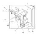
- FIG. 1is a view showing the configuration of an in-line heat treatment apparatus according to an embodiment of the present invention.
- Figure 2is an exploded perspective view showing the configuration of the in-line heat treatment apparatus according to an embodiment of the present invention.
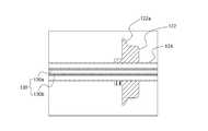
- FIG. 3is a detailed view of portion A of FIG. 1.
- FIG. 4is a view showing a connection state of the rotating shaft, the drive pulley and the heater in FIG.
- FIG. 5is a sectional view taken along the line B-B in FIG.
- FIG. 6is a sectional view taken along the line C-C in FIG.
- FIG. 7is a view illustrating an example of a heater as a detailed view of part D of FIG. 6.
- FIG. 8is a diagram illustrating another example of the heater as a detailed view of part D of FIG. 6.
- an inline heat treatment apparatusthat can continuously heat treatment the substrate, the chamber providing a heat treatment space for the substrate and the opening is formed opposite to the front and rear;
- a driving roller unitincluding a driving roller which moves while supporting the substrate and a rotating shaft having a hollow shape penetrating the driving roller; And a heater disposed inside the rotation shaft, wherein the driving roller unit is provided in plural along the moving direction of the substrate to load the substrate into the chamber and to unload the substrate from the chamber. Both ends are fixed to the outer wall of the chamber, characterized in that not interlocked with the operation of the rotating shaft.
- the driving roller unitmay be installed to be perpendicular to the loading and unloading direction of the substrate.
- the plurality of driving roller unitsmay interlock with each other.
- An interlocking pulleyinstalled at one end of each of the plurality of rotation shafts; And an interlocking belt for connecting the plurality of interlocking pulleys, and the plurality of driving roller units may interlock with each other as one of the plurality of interlocking pulleys is driven.
- One end of the rotating shaftmay be connected to a drive pulley for receiving an external drive force.
- Terminals for receiving external powermay be installed at both ends of the heater.
- Fixing flangesmay be installed at both ends of the heater to fix the heater to the outer wall of the chamber.
- the heatermay be heated by a pipe through which cooling water or cooling gas flows and an external power source, and a heating wire surrounding the outer circumferential surface of the tube may be installed in the heater.
- Conductors receiving power from the outsidemay be installed at both ends of the heater, and a heating element may be installed at the inner center of the heater to generate heat by receiving power from the conductor.
- the length of the heating elementmay be formed to correspond to the length of the substrate.
- FIG. 1is a view showing the configuration of an in-line heat treatment apparatus 100 according to an embodiment of the present invention.
- FIG. 2is an exploded perspective view showing the configuration of the in-line heat treatment apparatus 100 according to an embodiment of the present invention.
- FIG. 3is a view illustrating a portion A of FIG. 1.
- FIG. 4is a view illustrating a connection state of the rotation shaft 124, the driving pulley 126, and the heater 130 in FIG. 3.
- FIG. 5is a cross-sectional view illustrating a cross section of the B-B line of FIG. 3.
- FIG. 6is a cross-sectional view showing a cross section of the C-C line of FIG.
- FIG. 7illustrates an example of the heater 130 as a detailed view of part D of FIG. 6.
- FIG. 8shows another example of the heater 130 as a detailed view of part D of FIG.
- the inline heat treatment apparatus 100includes a chamber 110 in which a heat treatment space is provided, and a heating heater (not shown) installed inside or outside the chamber 110 for heating a substrate (not shown). It may include a gas supply pipe (not shown) for supplying gas for the heat treatment process atmosphere composition and a gas exhaust pipe (not shown) for gas discharge.
- a gas supply pipe(not shown) for supplying gas for the heat treatment process atmosphere composition
- a gas exhaust pipe(not shown) for gas discharge.
- the configuration of the heating heater, the gas supply pipe, the gas exhaust pipeis well known in the art, so a detailed description thereof will be omitted.
- the material of the substrate loaded in the inline heat treatment apparatus 100 of the present inventionis not particularly limited and may be loaded with a substrate of various materials such as glass, plastic, polymer, silicon wafer, stainless steel, and the like.
- a descriptionwill be given assuming a rectangular glass substrate that is most commonly used in the field of flat panel displays such as LCDs and OLEDs or thin film silicon solar cells.
- the inline heat treatment apparatus 100 of the present inventionis a sheet type processing one substrate at a time, but is not necessarily limited thereto. Therefore, the inline heat treatment apparatus 100 of the present invention may be configured in a batch type capable of simultaneously processing a plurality of substrates according to the object of the present invention.
- FIG. 1 and 2illustrate an inla heat treatment apparatus 100 according to an embodiment of the present invention. More specifically, in FIG. 1, the direction is set to show a characteristic configuration of the inline heat treatment apparatus 100 according to an embodiment of the present invention, and FIG. 2 is an inline heat treatment apparatus according to an embodiment of the present invention. The configuration of 100 is shown in an exploded manner.
- the inline heat treatment apparatus 100may include a chamber 110.
- the chamber 110may be configured to substantially seal an inner space while the heat treatment process is performed to provide a space for heat treating the substrate.
- the shape of the chamber 110is not limited to a particular shape, but is preferably a rectangular parallelepiped, as shown in FIGS. 1 and 2.
- a first opening 112 having a predetermined width and heightmay be formed on the front surface of the chamber 110.
- the first opening 112may serve as a passage through which the substrate is loaded. Since the first opening 112 needs to be blocked to seal the inside of the chamber 110 while the heat treatment process is performed, a door (not shown) that opens and closes in the vertical direction may be installed in the first opening 112. .
- a second opening 114 having a predetermined width and heightmay be formed on the rear surface of the chamber 110 (that is, the opposite side of the first opening 112).
- the second opening 114may serve as a passage through which the substrate is unloaded.
- the second opening 114needs to be blocked to seal the inside of the chamber 110 while the heat treatment process is performed, and thus the second opening 114 is opened and closed in the vertical direction.
- a door(not shown) may be installed.
- a third opening 116 having a predetermined width and heightmay be formed on the upper surface of the chamber 110.
- repair and replacement of componentsfor example, a gas supply pipe and a gas exhaust pipe
- the third opening 116may need to be blocked for the interior of the chamber 110 to be sealed during the heat treatment process.
- An openable covermay be installed.
- a frame (not shown) supporting the chamber 110may be installed below the chamber 110.
- the material of the frameis preferably stainless steel, but is not necessarily limited thereto.
- the inline heat treatment apparatus 100may include a plurality of driving roller units installed in the chamber 110 along a moving direction of the substrate. 120 may be configured to be included.
- the plurality of driving roller units 120move the substrate loaded through the first opening 112, support the substrate during the heat treatment of the substrate, and the second opening 114 to unload the substrate after the heat treatment is completed. ) To perform the function.
- the plurality of drive roller unit 120is preferably installed in a direction perpendicular to the loading and unloading direction of the substrate. Also, in a similar sense, the plurality of driving roller units 120 may be installed at the same height inside the chamber 110.
- the in-line heat treatment apparatus 100may further include a linkage pulley 140 and the linkage belt 142, which will be described later.
- a separate driving roller unit(not shown) different from the driving roller unit 120 installed inside the chamber 110 is provided at the front and rear of the chamber 110.
- a plurality of first openings 112 and the second opening 114may be provided outside.
- Such a separate driving roller unitmay perform a function to facilitate loading and unloading of the substrate into the chamber 110. To multiply these functions.
- the driving roller unit 120 and the separate driving roller unit installed in the chamber 110are interlocked with each other.
- the driving roller unit 120may include a driving roller 122 and a rotating shaft 124.
- the driving roller 122may be formed along the outer circumferential surface of the rotating shaft 124, which will be described later, to be in contact with the lower surface of the substrate and to move and support the substrate. As shown in FIG. 2, a plurality of driving rollers 122 may be included in each driving roller unit 120. Accordingly, the movement and support of the substrate can be made more stable by the driving roller 122.
- the plurality of driving rollers 122 included in each of the driving roller units 120may be formed to have different widths according to the installation positions. It may be, but the diameter is preferably all formed the same.
- the number of the driving rollers 122 included in each driving roller unit 120is preferably determined in a range capable of stable movement and support of the substrate to be loaded.
- the departure prevention step 122amay serve to prevent the substrate from being separated from the normal position.
- the rotation shaft 124may be installed to penetrate the central axis of the driving roller 122 to perform a function of rotating the driving roller 122. More specifically, the rotation shaft 124 may receive a driving force from the outside to rotate about its longitudinal axis, thereby rotating the driving roller 122 formed along its outer circumferential surface.
- both ends of the rotation shaft 124may be rotatably connected to both walls of the chamber 110 via a mechanism such as a fixing flange 134 described later.
- the driving pulley 126may be installed at one end of the rotating shaft 124.
- the drive pulley 126may perform a function of transmitting a rotational driving force to the rotation shaft 124.
- the driving force of the motor 150may be received by the motor pulley 152 and the driving belt 128, and the driving force may be transmitted to the rotation shaft 124.
- the drive pulley 126may be installed at any position of the rotation shaft 124, but may be preferably installed at one end of the rotation shaft 124 extending out of the chamber 110 as shown in FIG. 4. More specifically, one end of the rotating shaft 124 may be extended to the outside of the chamber 110 through one side wall of the chamber 110, the driving pulley 126 to receive the driving force from the outside to the extended portion so ) Can be installed.
- the driving pulley 126may be installed at one end of each rotation shaft 124, but preferably may be installed on any one rotation shaft 124 of the plurality of rotation shaft 124 as shown in FIG. .
- the reason for installing in this wayis to facilitate the interlocking of the plurality of driving roller units 120. Interlocking of the driving roller unit 120 may be further embodied by the following configuration.
- the inline heat treatment apparatus 100may further include an interlocking pulley 140 and an interlocking belt 142.
- the interlocking pulley 140may be installed at one end of each of the plurality of rotation shafts 124 to perform a function of allowing the driving roller unit 120 to interlock.
- the interlocking belt 142may be installed to contact the outer circumferential surfaces of the plurality of interlocking pulleys 140 to perform a function of connecting the plurality of interlocking pulleys 140 with each other.
- the mechanism by which the drive roller unit 120 interlocks by the interlocking pulley 140 and the interlocking belt 142is as follows. First, when any one of the plurality of interlocking pulleys 140 is driven by receiving a driving force from the outside, the interlocking belt 142 in contact with the outer peripheral surface is driven. Accordingly, the other interlocking pulley 140 in contact with the interlocking belt 142 is sequentially driven, and as a result, the plurality of driving roller units 120 interlock with each other.
- all the driving roller units 120can interlock with each other when a driving force is transmitted to only one of the interlocking pulleys 140.
- the transmission of the driving forceis preferably performed by the driving pulley 126.
- the driving pulley 126is installed only on any one rotation shaft 124 of the plurality of rotation shafts 124. It is preferable.
- the driving pulley 126 and the interlocking pulley 140may be formed adjacent to each other.
- the fixing bracket 160 bent in a 'c' shapemay be installed on the outer wall of the chamber 110.
- the fixing bracket 160may be rotatably coupled to the rotating shaft 124 extending to the outside of the chamber 110, and a hole 162 through which the driving belt 128 passes may be formed at a lower portion thereof. Accordingly, the driving force of the motor 150 is transmitted to the drive pulley 126 through the drive belt 128 so that the rotation shaft 124 can smoothly rotate.
- the fixing bracket 160may have open both sides. Accordingly, the interlocking belt 142 can be passed through the open both sides of the fixing bracket 160, the linkage of the drive roller unit 120 can be made more smoothly.
- the tension pulley 154 for adjusting the tension of the interlocking belt 142is further installed in the chamber 110.
- the tension pulley 154is in close contact with the interlock belt 142 and adjusts the tension of the interlock belt 142 so that the driving force is easily transmitted. It is preferable that the tension pulley 154 is configured in plural and in close contact with the interlock belt 142 at a position between the plurality of interlock pulleys 140.
- the rotary shaft 124can be rotated by receiving an external driving force, and the plurality of rotary shafts 124 can be interlocked with each other, the components employed in the present invention and the operation thereof are not limited to the above. No.
- the rotating shaft 124may perform not only a function of rotating the driving roller 122, but also a function of providing a space for installing the heater 130 therein.
- the rotation shaft 124may be formed in a hollow shape in which a space is formed inward along the central axis.
- a heater 130which is a characteristic configuration of the present invention will be described.
- the inline heat treatment apparatus 100may include a heater 130.
- the heater 130may perform a function of generating heat by the power supplied from the outside and applying the heat to the substrate.
- the heater 130is disposed in the inner space of the rotating shaft 124, thereby enabling efficient heat treatment of the substrate, it is possible to maximize the space utilization in the chamber 110.
- both ends of the heater 130are fixed to both outer walls of the chamber 110. This is to prevent the heater 130 from being rotated even when the rotating shaft 124 is rotated to move the substrate, so as to facilitate maintenance of the heater 130 connected to the external terminal 132 and the like described later.
- the heater 130is disposed in the inner space of the rotation shaft 124, the length may be formed longer than the rotation shaft 124. Accordingly, both ends of the heater 130 are extended to the outside of the chamber 110 through both ends of the rotating shaft 124, so that both ends of the extended heater 130 can be fixed to both outer walls of the chamber 110. do.
- Fixing flanges 134may be installed at both ends of the heater 130 to fix the heater 130 to both outer walls of the chamber 110.
- the fixing flange 134may fix both ends of the heater 130 protruding from the rotation shaft 124 so that the heater 130 does not rotate even when the rotation shaft 124 rotates.
- the fixing flange 134may be positioned on the side of the fixing bracket 160 installed on the outer wall of the chamber 110 as shown in FIG. 3. have.
- the terminal 132may be installed at the extended portions of both ends of the heater 130.
- the terminal 132may perform a function of transferring external power to the heater 130 to allow the heater 130 to generate heat.
- the terminal 132 used in the present inventionis not particularly limited and various types of terminals may be used.
- the heater 130according to an embodiment of the present invention, the cooling water or the cooling gas flows in the tube is installed therein, the outer circumferential surface of the tube is configured to be installed in the form of heating wire to generate heat by an external power source. Can be. If it can be configured in this way, the specific configuration inside the heater 130 is not particularly limited, but preferably may be configured as shown in FIG.
- an outer circumferential surface of the first tube 130a and the first tube 130a having a hollow shapeis surrounded and spaced apart from the first tube 130a by a predetermined distance.
- tube 130b usedis arrange
- the outer circumferential surface of the second tube 130bis also spaced apart from the inner circumferential surface of the rotation shaft 124 by a predetermined distance.
- the first tube (a)may be spaced apart from the space between the first tube 130a and the second tube 130b.
- a coil-type hot wire (not shown) surrounding 130ais disposed.
- heat generated in the hot wireis applied to the substrate supported by the drive roller 122, so that the substrate can be subjected to heat treatment.
- the cooling water or the cooling gasmay flow to the inside of the first tube 130a to unload the substrate, thereby rapidly cooling the inside of the chamber 110.
- the material of the heating wiremay include nichrome
- the material of the first and second tubes 130a and 130bmay include quartz.
- a configuration in which the cooling water or the cooling gas is supplied and flows to the first pipe 130amay use the configurations disclosed in Korean Patent Application No. 2008-110813 and Korean Patent Application No. 2008-110814.
- the heater 130may be configured such that the conductor 130d is installed at both ends thereof, and the heating element 130c is installed at the center thereof. More specifically, referring to FIG. 8, a conductor 130d receiving external power through the terminal 132 is installed at both ends of the heater 130, and is supplied from the conductor 130d at the center of the heater 130.
- a heating element 130cmay be installed to generate heat with the received power and apply the heat to the substrate. By adopting such a configuration, heat can be preferentially generated in the heating element 130c, so that the substrate can be heat treated efficiently.
- the material of the heating element 130cmay include nichrome or Kanthal, and the material of the conductor 130d may include stainless steel (SUS).
- the heating element 130cmay be configured to correspond to the length of the substrate.
- the heat treatment for the substrate by the heat generated by the heater 130when the heat treatment for the substrate by the heat generated by the heater 130 is progressed, since the plate surface of the substrate is located in parallel with the heater 130, the heat generated from the heater 130 is uniformly applied to the entire substrate Uniform heat treatment can be achieved.
- the heater 130is disposed inside the rotating shaft 124, a space for installing the heater 130 in the chamber 110 may be reduced.
Landscapes
- Physics & Mathematics (AREA)
- Engineering & Computer Science (AREA)
- General Physics & Mathematics (AREA)
- Nonlinear Science (AREA)
- Manufacturing & Machinery (AREA)
- Condensed Matter Physics & Semiconductors (AREA)
- Computer Hardware Design (AREA)
- Microelectronics & Electronic Packaging (AREA)
- Power Engineering (AREA)
- Chemical & Material Sciences (AREA)
- Crystallography & Structural Chemistry (AREA)
- Optics & Photonics (AREA)
- Tunnel Furnaces (AREA)
- Container, Conveyance, Adherence, Positioning, Of Wafer (AREA)
- Furnace Details (AREA)
- Liquid Crystal (AREA)
Abstract
Description
Translated fromKorean본 발명은 기판에 대한 인라인 열처리 장치에 관한 것이다. 보다 상세하게는, 열처리를 위해 기판을 챔버로 로딩 및 언로딩하는 구동 롤러의 회전축 내부에 히터를 설치하여 기판에 대한 균일한 열처리를 수행할 수 있고 챔버 내부의 공간 활용도를 높일 수 있는 인라인 열처리 장치에 관한 것이다.The present invention relates to an inline heat treatment apparatus for a substrate. More specifically, in-line heat treatment apparatus which can perform a uniform heat treatment on the substrate by installing a heater inside the rotary shaft of the drive roller for loading and unloading the substrate into the chamber for heat treatment, and increase the space utilization inside the chamber It is about.
기판을 사용하여 LCD(Liquid Crystal Display), PDP(Plasma Display Panel) 및 OLED (Organic Light Emitting Diode) 등 평면 디스플레이를 제작하는 경우, 기판에 대하여 열처리 공정을 수행한다.When manufacturing a flat panel display such as a liquid crystal display (LCD), a plasma display panel (PDP), and an organic light emitting diode (OLED) using a substrate, a heat treatment process is performed on the substrate.
이를 위하여 종래에는 기판의 열처리를 위해 엔드 이펙터와 같은 이송 기구를 사용하여 챔버에 기판을 로딩한 후 열처리를 수행하였다. 그러나, 근래에 기판이 점차 대면적화 되고 있어 엔드 이펙터를 이용한 기판의 로딩 작업시 기판이 변형되거나 손상을 입는 등의 문제점이 대두되었다.To this end, conventionally, the substrate is loaded in a chamber using a transfer mechanism such as an end effector for heat treatment of the substrate, and then heat treatment is performed. However, in recent years, since the substrate has been gradually increased in size, problems such as deformation or damage of the substrate have arisen when loading the substrate using the end effector.
이러한 문제점을 해결하기 위하여 복수개의 구동 롤러를 챔버의 전후에 연속적으로 배치하고, 기판은 구동 롤러에 의해 챔버로 로딩되어 열처리 되도록 하며, 열처리가 종료되면 구동 롤러에 의해 언로딩되는 인라인(in-line) 방식의 열처리 장치가 개시되었다.In order to solve this problem, a plurality of drive rollers are continuously arranged before and after the chamber, and the substrate is loaded into the chamber by the drive rollers for heat treatment, and in-line that is unloaded by the drive rollers after the heat treatment is completed. The heat treatment apparatus of the type) was disclosed.
하지만 인라인 열처리 장치는 챔버의 내측에 구동 롤러와 구동 롤러의 동작을 위한 기기들이 설치될 뿐만 아니라 히터와 히터의 동작을 위한 기기들이 설치되므로 챔버의 공간이 협소해지는 문제점이 있었다.However, the inline heat treatment apparatus has a problem in that the space of the chamber is narrowed because the devices for the operation of the driving roller and the driving roller are installed inside the chamber as well as the devices for the operation of the heater and the heater.
챔버의 공간 확보를 위해서 챔버의 크기를 증대시키면 챔버의 제작비가 상승되는 문제점이 있었다.Increasing the size of the chamber to secure the space of the chamber has a problem that the manufacturing cost of the chamber is increased.
또한, 대면적인 기판에 대한 균일한 열처리를 위해 챔버 내부에 히터를 균일하게 설치할 필요가 있으나, 챔버의 내부 공간이 협소해지는 문제가 있어 히터의 설치가 어려운 문제점이 있었다.In addition, it is necessary to uniformly install a heater inside the chamber for uniform heat treatment of the large-area substrate, but there is a problem that the installation of the heater is difficult because the internal space of the chamber is narrowed.
이에 본 발명은 상기와 같은 종래기술의 문제점을 해결하기 위한 것으로서, 대면적 기판을 챔버로 로딩 및 언로딩하는 구동 롤러의 회전축에 히터를 설치하여 기판에 대한 효율적인 열처리를 수행할 수 있는 인라인 열처리 장치를 제공하는 것을 목적으로 한다.Accordingly, the present invention is to solve the problems of the prior art as described above, in-line heat treatment apparatus that can perform a heat treatment on the substrate by installing a heater on the rotary shaft of the drive roller for loading and unloading a large area substrate into the chamber The purpose is to provide.
또한, 기판을 챔버로 로딩 및 언로딩하는 구동 롤러의 회전축에 히터를 설치함으로써 챔버 내부의 공간 활용도를 높일 수 있는 인라인 열처리 장치를 제공하는 것을 목적으로 한다.In addition, an object of the present invention is to provide an inline heat treatment apparatus capable of increasing space utilization inside a chamber by installing a heater on a rotating shaft of a driving roller for loading and unloading a substrate into a chamber.
상기와 같이 구성된 본 발명에 따르면, 챔버의 내측에 배치되어 기판을 로딩 및 언로딩하는 구동 롤러의 회전축에 히터가 설치되어 있어 회전축에서 설치된 히터에서 기판에 대하여 균일한 열 공급이 가능하므로 효율적인 열처리가 이루어지는 효과가 있다.According to the present invention configured as described above, the heater is installed on the rotating shaft of the drive roller disposed inside the chamber for loading and unloading the substrate, so that uniform heat supply to the substrate is possible in the heater installed at the rotating shaft, so that efficient heat treatment is achieved. It has an effect.
또한, 본 발명에 따르면, 대면적 기판을 챔버로 로딩 및 언로딩하는 구동 롤러의 회전축 내부에 히터를 설치함으로써 챔버 내부의 기기 설치 공간을 감소시켜 챔버의 내부 공간 활용도를 향상시킬 수 있는 인라인 열처리 장치를 제공하는 데 있다.In addition, according to the present invention, by installing a heater in the rotary shaft of the drive roller for loading and unloading a large area substrate into the chamber, in-line heat treatment apparatus that can reduce the equipment installation space inside the chamber to improve the internal space utilization of the chamber To provide.
도 1은 본 발명의 일 실시예에 따른 인라인 열처리 장치의 구성을 나타내는 도면이다.1 is a view showing the configuration of an in-line heat treatment apparatus according to an embodiment of the present invention.
도 2는 본 발명의 일 실시예에 따른 인라인 열처리 장치의 구성을 나타내는 분해 사시도이다.Figure 2 is an exploded perspective view showing the configuration of the in-line heat treatment apparatus according to an embodiment of the present invention.
도 3은 도 1의 A 부분의 상세도면이다.FIG. 3 is a detailed view of portion A of FIG. 1.
도 4는 도 3에서 회전축, 구동 풀리 및 히터의 연결 상태를 나타내는 도면이다.4 is a view showing a connection state of the rotating shaft, the drive pulley and the heater in FIG.
도 5는 도 3의 B-B 선의 선단면도이다.5 is a sectional view taken along the line B-B in FIG.
도 6은 도 1의 C-C 선의 선단면도이다.6 is a sectional view taken along the line C-C in FIG.
도 7은 도 6의 D 부분의 상세도면으로서 히터의 일 예를 나타내는 도면이다.7 is a view illustrating an example of a heater as a detailed view of part D of FIG. 6.
도 8은 도 6의 D 부분의 상세도면으로서 히터의 다른 예를 나타내는 도면이다.FIG. 8 is a diagram illustrating another example of the heater as a detailed view of part D of FIG. 6.
<도면의 주요 부분에 대한 부호의 설명><Explanation of symbols for the main parts of the drawings>
100: 인라인 열처리 장치100: inline heat treatment device
110: 챔버110: chamber
112: 제1 개구112: first opening
114: 제2 개구114: second opening
116: 제3 개구116: third opening
120: 구동 롤러 유닛120: drive roller unit
122: 구동 롤러122: drive roller
124: 회전축124: axis of rotation
126: 구동 풀리126: driven pulley
128: 구동 벨트128: drive belt
130: 히터130: heater
132: 단자132: terminal
134: 고정 플랜지134: fixed flange
140: 연동 풀리140: interlock pulley
142: 연동 벨트142: interlock belt
150: 모터150: motor
152: 모터 풀리152: motor pulley
154: 텐션 풀리154: tension pulley
160: 고정 브라켓160: fixing bracket
162: 홀162: hall
상술한 목적을 달성하기 위하여 본 발명에 따른 인라인 열처리 장치는, 기판을 연속적으로 열처리할 수 있는 인라인 열처리 장치로서, 상기 기판에 대한 열처리 공간을 제공하며 전후에 개구가 대향하여 형성되어 있는 챔버; 상기 기판을 지지하면서 이동시키는 구동 롤러와 상기 구동 롤러를 관통하는 중공 형태의 회전축을 포함하는 구동 롤러 유닛; 및 상기 회전축의 내측에 배치되는 히터 를 포함하고, 상기 구동 롤러 유닛은 상기 기판의 이동 방향을 따라 복수개로 설치되어 상기 챔버로 상기 기판을 로딩 및 상기 챔버로부터 상기 기판을 언로딩하며, 상기 히터의 양단은 상기 챔버의 외벽에 고정되어 상기 회전축의 동작과 연동되지 않는 것을 특징으로 한다.Inline heat treatment apparatus according to the present invention to achieve the above object, an inline heat treatment apparatus that can continuously heat treatment the substrate, the chamber providing a heat treatment space for the substrate and the opening is formed opposite to the front and rear; A driving roller unit including a driving roller which moves while supporting the substrate and a rotating shaft having a hollow shape penetrating the driving roller; And a heater disposed inside the rotation shaft, wherein the driving roller unit is provided in plural along the moving direction of the substrate to load the substrate into the chamber and to unload the substrate from the chamber. Both ends are fixed to the outer wall of the chamber, characterized in that not interlocked with the operation of the rotating shaft.
상기 구동 롤러 유닛은 상기 기판의 로딩 및 언로딩 방향에 대하여 직교하여 설치될 수 있다.The driving roller unit may be installed to be perpendicular to the loading and unloading direction of the substrate.
상기 복수개의 구동 롤러 유닛은 서로 연동할 수 있다.The plurality of driving roller units may interlock with each other.
상기 복수개의 회전축 각각의 일단에 설치되는 연동 풀리; 및 상기 복수개의 연동 풀리를 연결시키는 연동 벨트를 더 포함하며, 상기 복수개의 연동 풀리 중에서 어느 하나가 구동됨에 따라 상기 복수개의 구동 롤러 유닛이 서로 연동할 수 있다.An interlocking pulley installed at one end of each of the plurality of rotation shafts; And an interlocking belt for connecting the plurality of interlocking pulleys, and the plurality of driving roller units may interlock with each other as one of the plurality of interlocking pulleys is driven.
상기 회전축의 일단에는 외부의 구동력을 공급받기 위한 구동 풀리가 연결될 수 있다.One end of the rotating shaft may be connected to a drive pulley for receiving an external drive force.
상기 히터의 양단에는 외부의 전원을 공급받기 위한 단자가 설치될 수 있다.Terminals for receiving external power may be installed at both ends of the heater.
상기 히터의 양단에는 상기 히터를 상기 챔버의 외벽에 고정시키는 고정 플랜지가 설치될 수 있다.Fixing flanges may be installed at both ends of the heater to fix the heater to the outer wall of the chamber.
상기 히터의 내부에는 냉각 용수 또는 냉각 가스가 흐르는 관 및 외부 전원에 의하여 발열하며 상기 관의 외주면을 감싸는 열선이 설치될 수 있다.The heater may be heated by a pipe through which cooling water or cooling gas flows and an external power source, and a heating wire surrounding the outer circumferential surface of the tube may be installed in the heater.
상기 히터의 내부 양단에는 외부로부터 전원을 공급받는 전도체가 설치되며 상기 히터의 내부 중앙에는 상기 전도체로부터 전원을 전달받아 발열하는 발열체가 설치될 수 있다Conductors receiving power from the outside may be installed at both ends of the heater, and a heating element may be installed at the inner center of the heater to generate heat by receiving power from the conductor.
상기 발열체의 길이는 상기 기판의 길이에 대응되게 형성될 수 있다.The length of the heating element may be formed to correspond to the length of the substrate.
이하 첨부된 도면을 참조하여 본 발명의 구성을 상세하게 설명하도록 한다.Hereinafter, the configuration of the present invention will be described in detail with reference to the accompanying drawings.
도 1은 본 발명의 일 실시예에 따른 인라인 열처리 장치(100)의 구성을 나타내는 도면이다.1 is a view showing the configuration of an in-line
도 2는 본 발명의 일 실시예에 따른 인라인 열처리 장치(100)의 구성을 나타내는 분해 사시도이다.2 is an exploded perspective view showing the configuration of the in-line
도 3은 도 1의 A 부분을 나타내는 도면이다.3 is a view illustrating a portion A of FIG. 1.
도 4는 도 3에서 회전축(124), 구동 풀리(126) 및 히터(130)의 연결 상태를 나타내는 도면이다.4 is a view illustrating a connection state of the
도 5는 도 3의 B-B 선의 단면을 나타내는 선단면도이다.FIG. 5 is a cross-sectional view illustrating a cross section of the B-B line of FIG. 3.
도 6은 도 1의 C-C 선의 단면을 나타내는 선단면도이다.6 is a cross-sectional view showing a cross section of the C-C line of FIG.
도 7은 도 6의 D 부분의 상세도면으로서 히터(130)의 일 예를 나타낸다.FIG. 7 illustrates an example of the
도 8은 도 6의 D 부분의 상세도면으로서 히터(130)의 다른 예를 나타낸다.FIG. 8 shows another example of the
먼저, 본 발명의 인라인 열처리 장치(100)는 내부에 열처리 공간이 제공되는 챔버(110), 기판(미도시)을 가열하기 위한 챔버(110)의 내부 또는 외부에 설치되는 가열 히터(미도시), 열처리 공정 분위기 조성을 위한 가스를 공급하는 가스 공급관(미도시) 및 가스 배출을 위한 가스 배기관(미도시)을 포함하여 구성될 수 있다. 여기서 가열 히터, 가스 공급관, 가스 배기관의 구성은 이 분야에서는 널리 알려져 있는 공지 기술이므로 이에 대한 상세한 설명은 생략한다.First, the inline
또한, 본 발명의 인라인 열처리 장치(100)에 로딩되는 기판의 재질은 특별히 제한되지 않으며 글래스, 플라스틱, 폴리머, 실리콘 웨이퍼, 스테인레스 스틸 등 다양한 재질의 기판이 로딩될 수 있다. 이하에서는 LCD나 OLED와 같은 평판 디스플레이나 박막형 실리콘 태양전지 분야에 가장 일반적으로 사용되는 직사각형 형상의 글래스 기판을 상정하여 설명한다.In addition, the material of the substrate loaded in the inline
또한, 도 1 내지 도 8에는 본 발명의 인라인 열처리 장치(100)가 한 번에 한 개의 기판을 처리하는 매엽식인 것으로 도시되어 있으나 반드시 이에 한정되지는 아니한다. 따라서, 본 발명의 인라인 열처리 장치(100)는 본 발명이 이용되는 목적에 따라 복수개의 기판을 동시에 처리할 수 있는 배치식으로 구성될 수도 있다.In addition, it is shown in Figures 1 to 8 that the inline
도 1 및 도 2에서는 본 발명의 일 실시예에 따른 인라의 열처리 장치(100)를 도시하고 있다. 보다 구체적으로, 도 1에서는 본 발명의 일 실시예에 따른 인라인 열처리 장치(100)의 특징적인 구성이 부각되도록 방향을 설정하여 도시하고 있고, 도 2는 본 발명의 일 실시예에 따른 인라인 열처리 장치(100)의 구성을 분해하여 도시하고 있다.1 and 2 illustrate an inla
도 1 및 도 2를 참조하면, 본 발명의 일 실시예에 따른 인라인 열처리 장치(100)는 챔버(110)를 포함하여 구성될 수 있다. 챔버(110)는 열처리 공정이 수행되는 동안 실질적으로 내부 공간이 밀폐되도록 구성되어 기판을 열처리하기 위한 공간을 제공하는 기능을 수행할 수 있다. 챔버(110)의 형상은 특별한 형태로 제한되지 아니하나, 도 1 및 도 2에 도시된 바와 같이, 직육면체인 것이 바람직하다.1 and 2, the inline
도 1 및 도 2를 더 참조하면, 챔버(110)의 전면에는 소정의 너비와 높이를 가지는 제1 개구(112)가 형성될 수 있다. 이러한 제1 개구(112)는 기판이 로딩되는 통로로서의 역할을 수행할 수 있다. 열처리 공정이 수행되는 동안에는 챔버(110) 내부의 밀폐를 위하여 제1 개구(112)가 차단될 필요가 있으므로, 제1 개구(112)에는 상하 방향으로 개폐되는 도어(미도시)가 설치될 수 있다.1 and 2, a
도 1 및 도 2를 더 참조하면, 챔버(110)의 후면(즉, 제1 개구(112)의 반대측)에는 소정의 너비와 높이를 가지는 제2 개구(114)가 형성될 수 있다. 이러한 제2 개구(114)는 기판이 언로딩되는 통로로서의 역할을 수행할 수 있다. 제1 개구(112)와 유사하게, 열처리 공정이 수행되는 동안에는 챔버(110) 내부의 밀폐를 위하여 제2 개구(114)가 차단될 필요가 있으므로, 제2 개구(114)에는 상하 방향으로 개폐되는 도어(미도시)가 설치될 수 있다.1 and 2, a
도 1 및 도 2를 더 참조하면, 챔버(110)의 상부면에는 소정의 너비와 높이를 가지는 제3 개구(116)가 형성될 수 있다. 이러한 제3 개구(116)를 통해서는 챔버(110)의 내부에 설치되는 구성요소(예를 들어, 가스 공급관 및 가스 배기관 등)의 수리 및 교체가 이루어 질 수 있다. 제1 및 제2 개구(112, 114)와 유사하게, 열처리 공정이 수행되는 동안에는 챔버(110) 내부의 밀폐를 위하여 제3 개구(116)가 차단될 필요가 있으므로, 제3 개구(116)에는 개폐 가능한 커버가 설치될 수 있다.1 and 2, a
한편, 도 1 및 도 2에는 도시되지 않았지만, 챔버(110)의 하측에는 챔버(110)를 지지하는 프레임(미도시)이 설치될 수 있다. 이러한 프레임의 재질은 스테인레스 스틸인 것이 바람직하나 반드시 이에 한정되는 것은 아니다.Meanwhile, although not shown in FIGS. 1 and 2, a frame (not shown) supporting the
다음으로, 도 1 및 도 2를 더 참조하면, 본 발명의 일 실시예에 따른 인라인 열처리 장치(100)는 기판의 이동 방향을 따라 챔버(110)의 내부에 복수개로 설치되는 복수개의 구동 롤러 유닛(120)을 포함하여 구성될 수 있다. 이러한 복수개의 구동 롤러 유닛(120)은 제1 개구(112)를 통해 로딩된 기판을 이동시키고, 기판에 대한 열처리 도중 기판을 지지하며, 열처리가 종료된 기판을 언로딩하기 위해 제2 개구(114)로 이동시키는 기능을 수행할 수 있다.Next, referring further to FIGS. 1 and 2, the inline
이러한 기능을 원활하게 수행하기 위하여, 도 1 및 도 2에 도시된 바와 같이, 복수개의 구동 롤러 유닛(120)은 기판의 로딩 및 언로딩 방향에 대하여 직교하는 방향으로 설치되는 것이 바람직하다. 또한, 유사한 의미에서, 복수개의 구동 롤러 유닛(120)은 챔버(110) 내부에 동일한 높이로 설치되는 것이 바람직하다.In order to perform this function smoothly, as shown in Figures 1 and 2, the plurality of
또한, 유사한 의미에서, 복수개의 구동 롤러 유닛(120)은 연동하는(즉, 어느 하나의 구동 롤러 유닛(120)이 동작하면 다른 구동 롤러 유닛(120)도 함께 동작하는) 것이 바람직하다. 이를 위하여, 인라인 열처리 장치(100)는 연동 풀리(140) 및 연동 벨트(142)를 더 포함하여 구성될 수 있는데, 이에 대해서는 후술하도록 하겠다.Also, in a similar sense, it is preferable that the plurality of
또한, 도 1 및 도 2에는 도시되지 않았지만, 챔버(110) 내부에 설치되는 구동 롤러 유닛(120)과는 다른 별도의 구동 롤러 유닛(미도시)이 챔버(110)의 전방과 후방 즉, 제1 개구(112)와 제2 개구(114) 외측에 각각 복수개로 설치될 수 있다. 이러한 별도의 구동 롤러 유닛은 챔버(110)로의 기판의 로딩 및 언로딩이 용이하게 이루어지도록 하는 기능을 수행할 수 있다. 이러한 기능을 배가시키기 위하여. 챔버(110) 내부에 설치되는 구동 롤러 유닛(120)과 별도의 구동 롤러 유닛은 서로 연동되는 것이 바람직하다.In addition, although not shown in FIGS. 1 and 2, a separate driving roller unit (not shown) different from the driving
한편, 도 1 및 도 2를 더 참조하면, 구동 롤러 유닛(120)은 구동 롤러(122) 및 회전축(124)을 포함하여 구성될 수 있다.Meanwhile, referring to FIGS. 1 and 2, the driving
먼저, 구동 롤러(122)는 후술하는 회전축(124)의 외주면을 따라 형성되어 기판의 하면과 접촉하며 기판을 이동 및 지지시키는 기능을 수행할 수 있다. 도 2에 도시된 바와 같이, 구동 롤러(122)는 각 구동 롤러 유닛(120)에 복수개로 포함되는 것이 바람직하다. 이에 따라, 구동 롤러(122)에 의하여 기판의 이동 및 지지가 보다 안정적으로 이루어질 수 있게 된다.First, the driving
이처럼 구동 롤러(122)가 각 구동 롤러 유닛(120)에 복수개로 포함되는 경우, 각 구동 롤러 유닛(120)에 포함되는 복수개의 구동 롤러(122)는, 설치 위치에 따라 서로 다른 폭으로 형성될 수 있으나, 직경은 모두 동일하게 형성되는 것이 바람직하다. 또한, 각 구동 롤러 유닛(120)에 포함되는 구동 롤러(122)의 개수는 로딩되는 기판의 안정적인 이동과 지지를 할 수 있는 범위에서 결정되는 것이 바람직하다.As such, when the driving
한편, 도 7 및 도 8에 도시된 바와 같이, 각 구동 롤러 유닛(120)에 포함되는 복수개의 구동 롤러(122) 중에서, 양측 외곽에 배치되는 구동 롤러(122)의 외주면 일측에는 이탈 방지턱(122a)이 형성될 수 있다. 이러한 이탈 방지턱(122a)은 기판이 정규 위치에서 이탈하는 것을 방지하는 기능을 수행할 수 있다.On the other hand, as shown in Figures 7 and 8, out of the plurality of driving
다음으로, 회전축(124)은 구동 롤러(122)의 중심축을 관통하도록 설치되어 구동 롤러(122)를 회전시키는 기능을 수행할 수 있다. 보다 구체적으로, 회전축(124)은 외부로부터 구동력을 전달받아 그 길이 방향 축을 중심으로 회전하여, 그 외주면을 따라 형성되는 구동 롤러(122)를 회전시키는 기능을 수행할 수 있다.Next, the
구동 롤러(122)를 회전시키기 위하여, 회전축(124)의 양단은 후술하는 고정 플랜지(134)와 같은 기구를 매개로 챔버(110)의 양측 벽에 회전 가능하게 연결될 수 있다. 또한, 외부로부터 구동력을 전달받기 위하여, 회전축(124)의 일단에는 구동 풀리(126)가 설치될 수 있다. 구동 풀리(126)는 회전 구동력을 회전축(124)으로 전달하는 기능을 수행할 수 있는데. 예를 들어, 도 4에 도시된 바와 같이 모터 풀리(152) 및 구동 벨트(128)에 의해 모터(150)의 구동력을 전달받고 그 구동력을 회전축(124)으로 전달하는 기능을 수행할 수 있다.In order to rotate the driving
구동 풀리(126)는 회전축(124)의 어느 위치에도 설치될 수 있으나, 바람직하게는 도 4에 도시된 바와 같이 챔버(110)의 외부로 연장된 회전축(124)의 일단에 설치될 수 있다. 보다 구체적으로, 회전축(124)의 일단은 챔버(110)의 일측 벽을 통해 챔버(110)의 외부로 길게 연장될 수 있는데, 이렇게 연장된 부위에 외부에서 구동력을 전달받을 수 있도록 구동 풀리(126)가 설치될 수 있다.The
또한, 구동 풀리(126)는 각 회전축(124)의 일단에 설치될 수도 있으나, 바람직하게는 도 2에 도시된 바와 같이 복수개의 회전축(124) 중에서 어느 하나의 회전축(124)에 설치될 수 있다. 이와 같이 설치하는 이유는 복수개의 구동 롤러 유닛(120)을 서로 연동시키기 용이하게 하기 위함이다. 이러한 구동 롤러 유닛(120)의 연동은 다음과 같은 구성에 의해서 더욱 구체화될 수 있다.In addition, the driving
도 4를 참조하면, 앞서 언급한 바와 같이, 인라인 열처리 장치(100)는 연동 풀리(140) 및 연동 벨트(142)를 더 포함하여 구성될 수 있다. 연동 풀리(140)는 복수개의 회전축(124) 각각의 일단에 설치되어 구동 롤러 유닛(120)이 연동할 수 있도록 하는 기능을 수행할 수 있으며. 연동 벨트(142)는 복수개의 연동 풀리(140)의 외주면에 접촉하도록 설치되어 복수개의 연동 풀리(140)를 서로 연결시키는 기능을 수행할 수 있다.Referring to FIG. 4, as mentioned above, the inline
이러한 연동 풀리(140)와 연동 벨트(142)에 의하여 구동 롤러 유닛(120)이 연동하는 메커니즘은 다음과 같다. 먼저, 복수개의 연동 풀리(140) 중에서 어느 하나의 연동 풀리(140)가 외부로부터 구동력을 전달받아 구동하면, 그 외주면과 접촉하고 있는 연동 벨트(142)가 구동한다. 이에 따라, 연동 벨트(142)와 접촉하고 있는 다른 연동 풀리(140)가 순차적으로 구동하게 되며, 결과적으로 복수개의 구동 롤러 유닛(120)이 서로 연동하게 된다.The mechanism by which the
이러한 메커니즘을 살펴보면, 어느 하나의 연동 풀리(140)에만 구동력이 전달되면 모든 구동 롤러 유닛(120)이 서로 연동할 수 있음을 알 수 있다. 이러한 구동력의 전달은 도 4에 도시된 바와 같이 구동 풀리(126)에 의하여 수행되는 것이 바람직한데, 결과적으로 구동 풀리(126)는 복수개의 회전축(124) 중에서 어느 하나의 회전축(124)에만 설치되는 것이 바람직하다.Looking at such a mechanism, it can be seen that all the driving
이때 도 4에 도시된 바와 같이 구동 풀리(126)와 연동 풀리(140)는 서로 인접하여 형성될 수 있다. 이 경우, 구동 풀리(126) 및 연동 풀리(140)의 구동 메커니즘을 고려하여, 'ㄷ' 형태로 절곡된 고정 브라켓(160)이 챔버(110)의 외벽에 설치될 수 있다. 고정 브라켓(160)은 챔버(110)의 외부로 연장되는 회전축(124)과 회전 가능하게 결합될 수 있으며 그 하부에는 구동 벨트(128)가 통과하는 홀(162)이 형성될 수 있다. 이에 따라, 모터(150)의 구동력이 구동 벨트(128)를 매개로 구동 풀리(126)에 전달되어 회전축(124)이 원활하게 회전할 수 있게 된다. 또한, 고정 브라켓(160)은 개방된 양면을 가질 수 있다. 이에 따라, 연동 벨트(142)가 고정 브라켓(160)의 개방된 양면을 통하여 통과될 수 있게 되며, 구동 롤러 유닛(120)의 연동이 보다 원활하게 이루어질 수 있게 된다.In this case, as shown in FIG. 4, the driving
한편, 연동 풀리(140)와 연동 벨트(142)에 의하여 구동 롤러 유닛(120)이 연동하는 경우, 챔버(110)에는 연동 벨트(142)의 텐션을 조절하기 위한 텐션 풀리(154)가 더 설치될 수 있다. 도 4에 도시된 바와 같이, 텐션 풀리(154)는 연동 벨트(142)와 밀착하며 연동 벨트(142)의 텐션을 조절하여 구동력 전달이 용이하게 이루어지도록 한다. 텐션 풀리(154)는 복수개로 구성되어 복수개의 연동 풀리(140) 사이의 위치에서 연동 벨트(142)에 밀착되는 것이 바람직하다.On the other hand, when the
물론, 외부의 구동력을 전달받아 회전축(124)이 회전될 수 있고, 또한 복수개의 회전축(124)이 서로 연동될 수 있다면, 본 발명에 채용되는 구성 요소 및 이에 의한 동작 등은 상술한 바에 한정되지 아니한다.Of course, if the
한편, 회전축(124)은 구동 롤러(122)를 회전시키는 기능뿐만 아니라, 그 내부에 히터(130)가 설치되기 위한 공간을 제공하는 기능도 수행할 수 있다. 이를 위하여, 도 5에 도시된 바와 같이, 회전축(124)은 중심축을 따라 내측으로 공간이 형성되어 있는 중공 형태로 형성될 수 있다. 이하에서는 본 발명의 특징적 구성인 히터(130)에 대해서 살펴보기로 한다.On the other hand, the
도 5를 참조하면, 본 발명의 일 실시예에 따른 인라인 열처리 장치(100)는 히터(130)를 포함하여 구성될 수 있다. 히터(130)는 외부에서 공급되는 전원에 의해 열을 발생시켜 기판으로 인가하는 기능을 수행할 수 있다. 이러한 히터(130)는 회전축(124)의 내측 공간에 배치되는데, 이에 따라, 기판에 대한 효율적인 열처리를 수행할 수 있게 되며, 챔버(110) 내부의 공간 활용도를 극대화할 수 있게 된다.Referring to FIG. 5, the inline
또한, 도 5를 참조하면, 히터(130)의 양단은 챔버(110)의 양측 외벽에 고정된다. 이는, 회전축(124)이 기판의 이동을 위하여 회전될 때에도 히터(130)는 회전되지 않도록 하여, 후술하는 외부 단자(132) 등과 연결되는 히터(130)의 유지보수를 용이하게 하기 위함이다. 이를 위하여, 히터(130)는 회전축(124)의 내측 공간에 배치되되, 그 길이는 회전축(124) 보다 길게 형성될 수 있다. 이에 따라, 히터(130)의 양단은 회전축(124)의 양단을 통해 챔버(110) 외부로 연장되게 되는데, 이렇게 연장된 히터(130)의 양단이 챔버(110)의 양측 외벽에 고정될 수 있게 된다.5, both ends of the
히터(130)를 챔버(110)의 양측 외벽에 고정시키기 위하여 히터(130)의 양단에는 고정 플랜지(134)가 설치될 수 있다. 고정 플랜지(134)는 회전축(124)으로부터 돌출된 히터(130)의 양단을 고정하여 회전축(124)이 회전하여도 히터(130)가 회전하지 않도록 하는 기능을 수행할 수 있다. 이처럼 고정 플랜지(134)가 히터(130)의 양단에 설치되는 경우, 도 3에 도시된 바와 같이 챔버(110)의 외벽에 설치된 고정 브라켓(160)의 측면에 고정 플랜지(134)가 위치될 수 있다.Fixing
한편, 히터(130) 양단의 연장된 부분에는 단자(132)가 설치될 수 있다. 이러한 단자(132)는 외부의 전력을 히터(130)로 전달하여 히터(130)가 발열할 수 있도록 하는 기능을 수행할 수 있다. 본 발명에서 이용되는 단자(132)는 특별하게 한정되지 아니하며 다양한 종류의 단자가 이용될 수 있다.On the other hand, the terminal 132 may be installed at the extended portions of both ends of the
한편, 본 발명의 일 실시예에 따른 히터(130)는, 그 내부에 냉각 용수 또는 냉각 가스가 흐르는 관이 설치되고, 이러한 관의 외주면에 외부 전원에 의하여 발열하는 열선이 설치되는 형태로 구성될 수 있다. 이와 같은 형태로 구성될 수 있다면 히터(130) 내부의 구체적인 구성은 특별하게 한정되지 아니하나, 바람직하게는 도 7과 같이 구성될 수 있다.On the other hand, the
도 7을 참조하면, 히터(130)의 중심축 내부에는 중공 형태의 제1 관(130a) 및 제1 관(130a)의 외주면을 둘러싸며 제1 관(130a)과 소정의 거리만큼 이격되어 배치되는 제2 관(130b)이 배치되어 있다. 또한, 제2 관(130b)의 외주면 역시 회전축(124)의 내주면과 소정 거리만큼 이격되어 있으며, 도시되어 있지는 않지만 제1 관(130a)과 제2 관(130b)의 이격 공간에는 제1 관(130a)을 감싸는 코일형 열선(미도시)이 배치되어 있다. 이러한 구성을 채용함으로써, 열선에서 발열된 열이 구동 롤러(122)에 의해 지지되는 기판으로 인가되어 기판의 열처리를 진행할 수 있다. 또한, 열처리가 완료된 후에는 기판의 언로딩을 위해 제1 관(130a)의 내측으로 냉각용수 또는 냉각 가스가 흐르도록 하여 챔버(110) 내부의 냉각을 빠르게 진행할 수 있다.Referring to FIG. 7, inside the central axis of the
여기서, 열선의 재질은 니크롬을 포함할 수 있고, 제1 및 제2 관(130a, 130b)의 재질은 석영을 포함할 수 있다. 또한, 제1 관(130a)으로 냉각용수 또는 냉각 가스가 공급되어 흐르도록 하는 구성은 한국특허출원 2008-110813호 및 한국특허출원 2008-110814호에 개시되어 있는 구성을 이용할 수 있다.Here, the material of the heating wire may include nichrome, and the material of the first and
또한, 본 발명의 일 실시예에 따른 히터(130)는, 그 내부 양단에 전도체(130d)가 설치되고, 그 내부 중앙에 발열체(130c)가 설치되는 형태로 구성될 수 있다. 보다 구체적으로, 도 8을 참조하면, 히터(130) 내부 양단에 단자(132)를 통하여 외부의 전원을 공급받는 전도체(130d)가 설치되고, 히터(130) 내부 중앙에 전도체(130d)로부터 공급받은 전원으로 열을 발생시켜 기판으로 인가하는 발열체(130c)가 설치될 수 있다. 이와 같은 구성을 채용함으로써, 발열체(130c)에서 열을 우선적으로 발생시킬 수 있게 되므로, 효율적으로 기판을 열처리할 수 있게 된다.In addition, the
발열체(130c)의 재질은 니크롬 또는 칸탈(Kanthal)을 포함할 수 있고, 전도체(130d)의 재질은 스테인레스강(SUS)를 포함할 수 있다. 또한, 보다 효율적인 기판의 열처리를 위하여, 발열체(130c)를 기판의 길이에 대응되게 구성할 수 있다.The material of the
상기와 같이 구성된 인라인 열처리 장치(100)의 동작과 이에 의한 열처리 공정은 기존의 인라인 방식 열처리 장치와 동일한 방식으로 동작하므로 이에 대한 상세한 설명은 생략한다.Since the operation of the inline
본 발명에서는 히터(130)에서 발열된 열에 의해 기판에 대한 열처리가 진행될 때, 기판의 판면은 히터(130)와 평행하게 위치되므로 히터(130)에서 발생된 열은 기판 전체에 대하여 균일하게 인가되어 균일한 열처리가 이루어질 수 있다.In the present invention, when the heat treatment for the substrate by the heat generated by the
또한, 히터(130)는 회전축(124)의 내부에 배치되어 있으므로 챔버(110) 내부에서 히터(130)의 설치를 위한 공간이 감소될 수 있다.In addition, since the
본 발명은 상술한 바와 같이 바람직한 실시예를 들어 도시하고 설명하였으나, 상기 실시예에 한정되지 아니하며 본 발명의 정신을 벗어나지 않는 범위 내에서 당해 발명이 속하는 기술분야에서 통상의 지식을 가진 자에 의해 다양한 변형과 변경이 가능하다. 그러한 변형예 및 변경예는 본 발명과 첨부된 특허청구범위의 범위 내에 속하는 것으로 보아야 한다.Although the present invention has been illustrated and described with reference to the preferred embodiments as described above, the present invention is not limited to the above embodiments, and various modifications may be made by those skilled in the art without departing from the spirit of the present invention. Modifications and variations are possible. Such modifications and variations are intended to fall within the scope of the invention and the appended claims.
Claims (10)
Translated fromKoreanPriority Applications (2)
| Application Number | Priority Date | Filing Date | Title |
|---|---|---|---|
| JP2012501928AJP2012521653A (en) | 2009-03-23 | 2010-03-22 | In-line heat treatment equipment |
| CN2010800123656ACN102356455A (en) | 2009-03-23 | 2010-03-22 | In-line heat treatment apparatus |
Applications Claiming Priority (2)
| Application Number | Priority Date | Filing Date | Title |
|---|---|---|---|
| KR10-2009-0024465 | 2009-03-23 | ||
| KR1020090024465AKR101055862B1 (en) | 2009-03-23 | 2009-03-23 | Inline heat treatment equipment |
Publications (2)
| Publication Number | Publication Date |
|---|---|
| WO2010110558A2true WO2010110558A2 (en) | 2010-09-30 |
| WO2010110558A3 WO2010110558A3 (en) | 2010-12-23 |
Family
ID=42781641
Family Applications (1)
| Application Number | Title | Priority Date | Filing Date |
|---|---|---|---|
| PCT/KR2010/001736WO2010110558A2 (en) | 2009-03-23 | 2010-03-22 | In-line heat treatment apparatus |
Country Status (5)
| Country | Link |
|---|---|
| JP (1) | JP2012521653A (en) |
| KR (1) | KR101055862B1 (en) |
| CN (1) | CN102356455A (en) |
| TW (1) | TW201041045A (en) |
| WO (1) | WO2010110558A2 (en) |
Cited By (269)
| Publication number | Priority date | Publication date | Assignee | Title |
|---|---|---|---|---|
| US11001925B2 (en) | 2016-12-19 | 2021-05-11 | Asm Ip Holding B.V. | Substrate processing apparatus |
| US11004977B2 (en) | 2017-07-19 | 2021-05-11 | Asm Ip Holding B.V. | Method for depositing a group IV semiconductor and related semiconductor device structures |
| US11018002B2 (en) | 2017-07-19 | 2021-05-25 | Asm Ip Holding B.V. | Method for selectively depositing a Group IV semiconductor and related semiconductor device structures |
| US11015245B2 (en) | 2014-03-19 | 2021-05-25 | Asm Ip Holding B.V. | Gas-phase reactor and system having exhaust plenum and components thereof |
| US11022879B2 (en) | 2017-11-24 | 2021-06-01 | Asm Ip Holding B.V. | Method of forming an enhanced unexposed photoresist layer |
| US11031242B2 (en) | 2018-11-07 | 2021-06-08 | Asm Ip Holding B.V. | Methods for depositing a boron doped silicon germanium film |
| USD922229S1 (en) | 2019-06-05 | 2021-06-15 | Asm Ip Holding B.V. | Device for controlling a temperature of a gas supply unit |
| US11049751B2 (en) | 2018-09-14 | 2021-06-29 | Asm Ip Holding B.V. | Cassette supply system to store and handle cassettes and processing apparatus equipped therewith |
| US11053591B2 (en) | 2018-08-06 | 2021-07-06 | Asm Ip Holding B.V. | Multi-port gas injection system and reactor system including same |
| US11056344B2 (en) | 2017-08-30 | 2021-07-06 | Asm Ip Holding B.V. | Layer forming method |
| US11069510B2 (en) | 2017-08-30 | 2021-07-20 | Asm Ip Holding B.V. | Substrate processing apparatus |
| US11081345B2 (en) | 2018-02-06 | 2021-08-03 | Asm Ip Holding B.V. | Method of post-deposition treatment for silicon oxide film |
| US11088002B2 (en) | 2018-03-29 | 2021-08-10 | Asm Ip Holding B.V. | Substrate rack and a substrate processing system and method |
| US11087997B2 (en) | 2018-10-31 | 2021-08-10 | Asm Ip Holding B.V. | Substrate processing apparatus for processing substrates |
| US11094546B2 (en) | 2017-10-05 | 2021-08-17 | Asm Ip Holding B.V. | Method for selectively depositing a metallic film on a substrate |
| US11094582B2 (en) | 2016-07-08 | 2021-08-17 | Asm Ip Holding B.V. | Selective deposition method to form air gaps |
| US11101370B2 (en) | 2016-05-02 | 2021-08-24 | Asm Ip Holding B.V. | Method of forming a germanium oxynitride film |
| US11107676B2 (en) | 2016-07-28 | 2021-08-31 | Asm Ip Holding B.V. | Method and apparatus for filling a gap |
| US11114283B2 (en) | 2018-03-16 | 2021-09-07 | Asm Ip Holding B.V. | Reactor, system including the reactor, and methods of manufacturing and using same |
| US11114294B2 (en) | 2019-03-08 | 2021-09-07 | Asm Ip Holding B.V. | Structure including SiOC layer and method of forming same |
| USD930782S1 (en) | 2019-08-22 | 2021-09-14 | Asm Ip Holding B.V. | Gas distributor |
| US11127589B2 (en) | 2019-02-01 | 2021-09-21 | Asm Ip Holding B.V. | Method of topology-selective film formation of silicon oxide |
| US11127617B2 (en) | 2017-11-27 | 2021-09-21 | Asm Ip Holding B.V. | Storage device for storing wafer cassettes for use with a batch furnace |
| USD931978S1 (en) | 2019-06-27 | 2021-09-28 | Asm Ip Holding B.V. | Showerhead vacuum transport |
| US11139308B2 (en) | 2015-12-29 | 2021-10-05 | Asm Ip Holding B.V. | Atomic layer deposition of III-V compounds to form V-NAND devices |
| US11139191B2 (en) | 2017-08-09 | 2021-10-05 | Asm Ip Holding B.V. | Storage apparatus for storing cassettes for substrates and processing apparatus equipped therewith |
| US11158513B2 (en) | 2018-12-13 | 2021-10-26 | Asm Ip Holding B.V. | Methods for forming a rhenium-containing film on a substrate by a cyclical deposition process and related semiconductor device structures |
| US11164955B2 (en) | 2017-07-18 | 2021-11-02 | Asm Ip Holding B.V. | Methods for forming a semiconductor device structure and related semiconductor device structures |
| US11168395B2 (en) | 2018-06-29 | 2021-11-09 | Asm Ip Holding B.V. | Temperature-controlled flange and reactor system including same |
| USD935572S1 (en) | 2019-05-24 | 2021-11-09 | Asm Ip Holding B.V. | Gas channel plate |
| US11171025B2 (en) | 2019-01-22 | 2021-11-09 | Asm Ip Holding B.V. | Substrate processing device |
| US11205585B2 (en) | 2016-07-28 | 2021-12-21 | Asm Ip Holding B.V. | Substrate processing apparatus and method of operating the same |
| US11217444B2 (en) | 2018-11-30 | 2022-01-04 | Asm Ip Holding B.V. | Method for forming an ultraviolet radiation responsive metal oxide-containing film |
| US11222772B2 (en) | 2016-12-14 | 2022-01-11 | Asm Ip Holding B.V. | Substrate processing apparatus |
| USD940837S1 (en) | 2019-08-22 | 2022-01-11 | Asm Ip Holding B.V. | Electrode |
| US11227782B2 (en) | 2019-07-31 | 2022-01-18 | Asm Ip Holding B.V. | Vertical batch furnace assembly |
| US11227789B2 (en) | 2019-02-20 | 2022-01-18 | Asm Ip Holding B.V. | Method and apparatus for filling a recess formed within a substrate surface |
| US11230766B2 (en) | 2018-03-29 | 2022-01-25 | Asm Ip Holding B.V. | Substrate processing apparatus and method |
| US11232963B2 (en) | 2018-10-03 | 2022-01-25 | Asm Ip Holding B.V. | Substrate processing apparatus and method |
| US11242598B2 (en) | 2015-06-26 | 2022-02-08 | Asm Ip Holding B.V. | Structures including metal carbide material, devices including the structures, and methods of forming same |
| US11244825B2 (en) | 2018-11-16 | 2022-02-08 | Asm Ip Holding B.V. | Methods for depositing a transition metal chalcogenide film on a substrate by a cyclical deposition process |
| US11251035B2 (en) | 2016-12-22 | 2022-02-15 | Asm Ip Holding B.V. | Method of forming a structure on a substrate |
| US11251068B2 (en) | 2018-10-19 | 2022-02-15 | Asm Ip Holding B.V. | Substrate processing apparatus and substrate processing method |
| US11251040B2 (en) | 2019-02-20 | 2022-02-15 | Asm Ip Holding B.V. | Cyclical deposition method including treatment step and apparatus for same |
| USD944946S1 (en) | 2019-06-14 | 2022-03-01 | Asm Ip Holding B.V. | Shower plate |
| US11270899B2 (en) | 2018-06-04 | 2022-03-08 | Asm Ip Holding B.V. | Wafer handling chamber with moisture reduction |
| US11274369B2 (en) | 2018-09-11 | 2022-03-15 | Asm Ip Holding B.V. | Thin film deposition method |
| US11282698B2 (en) | 2019-07-19 | 2022-03-22 | Asm Ip Holding B.V. | Method of forming topology-controlled amorphous carbon polymer film |
| US11286558B2 (en) | 2019-08-23 | 2022-03-29 | Asm Ip Holding B.V. | Methods for depositing a molybdenum nitride film on a surface of a substrate by a cyclical deposition process and related semiconductor device structures including a molybdenum nitride film |
| US11286562B2 (en) | 2018-06-08 | 2022-03-29 | Asm Ip Holding B.V. | Gas-phase chemical reactor and method of using same |
| US11289326B2 (en) | 2019-05-07 | 2022-03-29 | Asm Ip Holding B.V. | Method for reforming amorphous carbon polymer film |
| US11295980B2 (en) | 2017-08-30 | 2022-04-05 | Asm Ip Holding B.V. | Methods for depositing a molybdenum metal film over a dielectric surface of a substrate by a cyclical deposition process and related semiconductor device structures |
| US11296189B2 (en) | 2018-06-21 | 2022-04-05 | Asm Ip Holding B.V. | Method for depositing a phosphorus doped silicon arsenide film and related semiconductor device structures |
| USD947913S1 (en) | 2019-05-17 | 2022-04-05 | Asm Ip Holding B.V. | Susceptor shaft |
| USD948463S1 (en) | 2018-10-24 | 2022-04-12 | Asm Ip Holding B.V. | Susceptor for semiconductor substrate supporting apparatus |
| USD949319S1 (en) | 2019-08-22 | 2022-04-19 | Asm Ip Holding B.V. | Exhaust duct |
| US11306395B2 (en) | 2017-06-28 | 2022-04-19 | Asm Ip Holding B.V. | Methods for depositing a transition metal nitride film on a substrate by atomic layer deposition and related deposition apparatus |
| US11315794B2 (en) | 2019-10-21 | 2022-04-26 | Asm Ip Holding B.V. | Apparatus and methods for selectively etching films |
| US11339476B2 (en) | 2019-10-08 | 2022-05-24 | Asm Ip Holding B.V. | Substrate processing device having connection plates, substrate processing method |
| US11342216B2 (en) | 2019-02-20 | 2022-05-24 | Asm Ip Holding B.V. | Cyclical deposition method and apparatus for filling a recess formed within a substrate surface |
| US11345999B2 (en) | 2019-06-06 | 2022-05-31 | Asm Ip Holding B.V. | Method of using a gas-phase reactor system including analyzing exhausted gas |
| US11355338B2 (en) | 2019-05-10 | 2022-06-07 | Asm Ip Holding B.V. | Method of depositing material onto a surface and structure formed according to the method |
| US11361990B2 (en) | 2018-05-28 | 2022-06-14 | Asm Ip Holding B.V. | Substrate processing method and device manufactured by using the same |
| US11374112B2 (en) | 2017-07-19 | 2022-06-28 | Asm Ip Holding B.V. | Method for depositing a group IV semiconductor and related semiconductor device structures |
| US11378337B2 (en) | 2019-03-28 | 2022-07-05 | Asm Ip Holding B.V. | Door opener and substrate processing apparatus provided therewith |
| US11387106B2 (en) | 2018-02-14 | 2022-07-12 | Asm Ip Holding B.V. | Method for depositing a ruthenium-containing film on a substrate by a cyclical deposition process |
| US11387120B2 (en) | 2017-09-28 | 2022-07-12 | Asm Ip Holding B.V. | Chemical dispensing apparatus and methods for dispensing a chemical to a reaction chamber |
| US11390950B2 (en) | 2017-01-10 | 2022-07-19 | Asm Ip Holding B.V. | Reactor system and method to reduce residue buildup during a film deposition process |
| US11390945B2 (en) | 2019-07-03 | 2022-07-19 | Asm Ip Holding B.V. | Temperature control assembly for substrate processing apparatus and method of using same |
| US11390946B2 (en) | 2019-01-17 | 2022-07-19 | Asm Ip Holding B.V. | Methods of forming a transition metal containing film on a substrate by a cyclical deposition process |
| US11393690B2 (en) | 2018-01-19 | 2022-07-19 | Asm Ip Holding B.V. | Deposition method |
| US11398382B2 (en) | 2018-03-27 | 2022-07-26 | Asm Ip Holding B.V. | Method of forming an electrode on a substrate and a semiconductor device structure including an electrode |
| US11396702B2 (en) | 2016-11-15 | 2022-07-26 | Asm Ip Holding B.V. | Gas supply unit and substrate processing apparatus including the gas supply unit |
| US11401605B2 (en) | 2019-11-26 | 2022-08-02 | Asm Ip Holding B.V. | Substrate processing apparatus |
| US11410851B2 (en) | 2017-02-15 | 2022-08-09 | Asm Ip Holding B.V. | Methods for forming a metallic film on a substrate by cyclical deposition and related semiconductor device structures |
| US11414760B2 (en) | 2018-10-08 | 2022-08-16 | Asm Ip Holding B.V. | Substrate support unit, thin film deposition apparatus including the same, and substrate processing apparatus including the same |
| US11417545B2 (en) | 2017-08-08 | 2022-08-16 | Asm Ip Holding B.V. | Radiation shield |
| US11424119B2 (en) | 2019-03-08 | 2022-08-23 | Asm Ip Holding B.V. | Method for selective deposition of silicon nitride layer and structure including selectively-deposited silicon nitride layer |
| US11430640B2 (en) | 2019-07-30 | 2022-08-30 | Asm Ip Holding B.V. | Substrate processing apparatus |
| US11430674B2 (en) | 2018-08-22 | 2022-08-30 | Asm Ip Holding B.V. | Sensor array, apparatus for dispensing a vapor phase reactant to a reaction chamber and related methods |
| US11437241B2 (en) | 2020-04-08 | 2022-09-06 | Asm Ip Holding B.V. | Apparatus and methods for selectively etching silicon oxide films |
| US11443926B2 (en) | 2019-07-30 | 2022-09-13 | Asm Ip Holding B.V. | Substrate processing apparatus |
| US11447861B2 (en) | 2016-12-15 | 2022-09-20 | Asm Ip Holding B.V. | Sequential infiltration synthesis apparatus and a method of forming a patterned structure |
| US11447864B2 (en) | 2019-04-19 | 2022-09-20 | Asm Ip Holding B.V. | Layer forming method and apparatus |
| US11453943B2 (en) | 2016-05-25 | 2022-09-27 | Asm Ip Holding B.V. | Method for forming carbon-containing silicon/metal oxide or nitride film by ALD using silicon precursor and hydrocarbon precursor |
| USD965044S1 (en) | 2019-08-19 | 2022-09-27 | Asm Ip Holding B.V. | Susceptor shaft |
| USD965524S1 (en) | 2019-08-19 | 2022-10-04 | Asm Ip Holding B.V. | Susceptor support |
| US11476109B2 (en) | 2019-06-11 | 2022-10-18 | Asm Ip Holding B.V. | Method of forming an electronic structure using reforming gas, system for performing the method, and structure formed using the method |
| US11473195B2 (en) | 2018-03-01 | 2022-10-18 | Asm Ip Holding B.V. | Semiconductor processing apparatus and a method for processing a substrate |
| US11482418B2 (en) | 2018-02-20 | 2022-10-25 | Asm Ip Holding B.V. | Substrate processing method and apparatus |
| US11482533B2 (en) | 2019-02-20 | 2022-10-25 | Asm Ip Holding B.V. | Apparatus and methods for plug fill deposition in 3-D NAND applications |
| US11482412B2 (en) | 2018-01-19 | 2022-10-25 | Asm Ip Holding B.V. | Method for depositing a gap-fill layer by plasma-assisted deposition |
| US11488854B2 (en) | 2020-03-11 | 2022-11-01 | Asm Ip Holding B.V. | Substrate handling device with adjustable joints |
| US11488819B2 (en) | 2018-12-04 | 2022-11-01 | Asm Ip Holding B.V. | Method of cleaning substrate processing apparatus |
| US11495459B2 (en) | 2019-09-04 | 2022-11-08 | Asm Ip Holding B.V. | Methods for selective deposition using a sacrificial capping layer |
| US11492703B2 (en) | 2018-06-27 | 2022-11-08 | Asm Ip Holding B.V. | Cyclic deposition methods for forming metal-containing material and films and structures including the metal-containing material |
| US11501973B2 (en) | 2018-01-16 | 2022-11-15 | Asm Ip Holding B.V. | Method for depositing a material film on a substrate within a reaction chamber by a cyclical deposition process and related device structures |
| US11501956B2 (en) | 2012-10-12 | 2022-11-15 | Asm Ip Holding B.V. | Semiconductor reaction chamber showerhead |
| US11499226B2 (en) | 2018-11-02 | 2022-11-15 | Asm Ip Holding B.V. | Substrate supporting unit and a substrate processing device including the same |
| US11501968B2 (en) | 2019-11-15 | 2022-11-15 | Asm Ip Holding B.V. | Method for providing a semiconductor device with silicon filled gaps |
| US11499222B2 (en) | 2018-06-27 | 2022-11-15 | Asm Ip Holding B.V. | Cyclic deposition methods for forming metal-containing material and films and structures including the metal-containing material |
| US11515187B2 (en) | 2020-05-01 | 2022-11-29 | Asm Ip Holding B.V. | Fast FOUP swapping with a FOUP handler |
| US11515188B2 (en) | 2019-05-16 | 2022-11-29 | Asm Ip Holding B.V. | Wafer boat handling device, vertical batch furnace and method |
| US11521851B2 (en) | 2020-02-03 | 2022-12-06 | Asm Ip Holding B.V. | Method of forming structures including a vanadium or indium layer |
| US11527400B2 (en) | 2019-08-23 | 2022-12-13 | Asm Ip Holding B.V. | Method for depositing silicon oxide film having improved quality by peald using bis(diethylamino)silane |
| US11527403B2 (en) | 2019-12-19 | 2022-12-13 | Asm Ip Holding B.V. | Methods for filling a gap feature on a substrate surface and related semiconductor structures |
| US11530483B2 (en) | 2018-06-21 | 2022-12-20 | Asm Ip Holding B.V. | Substrate processing system |
| US11530876B2 (en) | 2020-04-24 | 2022-12-20 | Asm Ip Holding B.V. | Vertical batch furnace assembly comprising a cooling gas supply |
| US11532757B2 (en) | 2016-10-27 | 2022-12-20 | Asm Ip Holding B.V. | Deposition of charge trapping layers |
| US11551912B2 (en) | 2020-01-20 | 2023-01-10 | Asm Ip Holding B.V. | Method of forming thin film and method of modifying surface of thin film |
| US11551925B2 (en) | 2019-04-01 | 2023-01-10 | Asm Ip Holding B.V. | Method for manufacturing a semiconductor device |
| USD975665S1 (en) | 2019-05-17 | 2023-01-17 | Asm Ip Holding B.V. | Susceptor shaft |
| US11557474B2 (en) | 2019-07-29 | 2023-01-17 | Asm Ip Holding B.V. | Methods for selective deposition utilizing n-type dopants and/or alternative dopants to achieve high dopant incorporation |
| US11562901B2 (en) | 2019-09-25 | 2023-01-24 | Asm Ip Holding B.V. | Substrate processing method |
| US11572620B2 (en) | 2018-11-06 | 2023-02-07 | Asm Ip Holding B.V. | Methods for selectively depositing an amorphous silicon film on a substrate |
| US11581186B2 (en) | 2016-12-15 | 2023-02-14 | Asm Ip Holding B.V. | Sequential infiltration synthesis apparatus |
| US11587815B2 (en) | 2019-07-31 | 2023-02-21 | Asm Ip Holding B.V. | Vertical batch furnace assembly |
| US11587821B2 (en) | 2017-08-08 | 2023-02-21 | Asm Ip Holding B.V. | Substrate lift mechanism and reactor including same |
| US11587814B2 (en) | 2019-07-31 | 2023-02-21 | Asm Ip Holding B.V. | Vertical batch furnace assembly |
| USD979506S1 (en) | 2019-08-22 | 2023-02-28 | Asm Ip Holding B.V. | Insulator |
| US11594450B2 (en) | 2019-08-22 | 2023-02-28 | Asm Ip Holding B.V. | Method for forming a structure with a hole |
| US11594600B2 (en) | 2019-11-05 | 2023-02-28 | Asm Ip Holding B.V. | Structures with doped semiconductor layers and methods and systems for forming same |
| USD980813S1 (en) | 2021-05-11 | 2023-03-14 | Asm Ip Holding B.V. | Gas flow control plate for substrate processing apparatus |
| USD980814S1 (en) | 2021-05-11 | 2023-03-14 | Asm Ip Holding B.V. | Gas distributor for substrate processing apparatus |
| US11605528B2 (en) | 2019-07-09 | 2023-03-14 | Asm Ip Holding B.V. | Plasma device using coaxial waveguide, and substrate treatment method |
| US11610775B2 (en) | 2016-07-28 | 2023-03-21 | Asm Ip Holding B.V. | Method and apparatus for filling a gap |
| US11610774B2 (en) | 2019-10-02 | 2023-03-21 | Asm Ip Holding B.V. | Methods for forming a topographically selective silicon oxide film by a cyclical plasma-enhanced deposition process |
| US11615970B2 (en) | 2019-07-17 | 2023-03-28 | Asm Ip Holding B.V. | Radical assist ignition plasma system and method |
| USD981973S1 (en) | 2021-05-11 | 2023-03-28 | Asm Ip Holding B.V. | Reactor wall for substrate processing apparatus |
| US11626316B2 (en) | 2019-11-20 | 2023-04-11 | Asm Ip Holding B.V. | Method of depositing carbon-containing material on a surface of a substrate, structure formed using the method, and system for forming the structure |
| US11626308B2 (en) | 2020-05-13 | 2023-04-11 | Asm Ip Holding B.V. | Laser alignment fixture for a reactor system |
| US11629406B2 (en) | 2018-03-09 | 2023-04-18 | Asm Ip Holding B.V. | Semiconductor processing apparatus comprising one or more pyrometers for measuring a temperature of a substrate during transfer of the substrate |
| US11629407B2 (en) | 2019-02-22 | 2023-04-18 | Asm Ip Holding B.V. | Substrate processing apparatus and method for processing substrates |
| US11637014B2 (en) | 2019-10-17 | 2023-04-25 | Asm Ip Holding B.V. | Methods for selective deposition of doped semiconductor material |
| US11637011B2 (en) | 2019-10-16 | 2023-04-25 | Asm Ip Holding B.V. | Method of topology-selective film formation of silicon oxide |
| US11639811B2 (en) | 2017-11-27 | 2023-05-02 | Asm Ip Holding B.V. | Apparatus including a clean mini environment |
| US11639548B2 (en) | 2019-08-21 | 2023-05-02 | Asm Ip Holding B.V. | Film-forming material mixed-gas forming device and film forming device |
| US11646205B2 (en) | 2019-10-29 | 2023-05-09 | Asm Ip Holding B.V. | Methods of selectively forming n-type doped material on a surface, systems for selectively forming n-type doped material, and structures formed using same |
| US11643724B2 (en) | 2019-07-18 | 2023-05-09 | Asm Ip Holding B.V. | Method of forming structures using a neutral beam |
| US11644758B2 (en) | 2020-07-17 | 2023-05-09 | Asm Ip Holding B.V. | Structures and methods for use in photolithography |
| US11646184B2 (en) | 2019-11-29 | 2023-05-09 | Asm Ip Holding B.V. | Substrate processing apparatus |
| US11646204B2 (en) | 2020-06-24 | 2023-05-09 | Asm Ip Holding B.V. | Method for forming a layer provided with silicon |
| US11646197B2 (en) | 2018-07-03 | 2023-05-09 | Asm Ip Holding B.V. | Method for depositing silicon-free carbon-containing film as gap-fill layer by pulse plasma-assisted deposition |
| US11649546B2 (en) | 2016-07-08 | 2023-05-16 | Asm Ip Holding B.V. | Organic reactants for atomic layer deposition |
| US11658035B2 (en) | 2020-06-30 | 2023-05-23 | Asm Ip Holding B.V. | Substrate processing method |
| US11658029B2 (en) | 2018-12-14 | 2023-05-23 | Asm Ip Holding B.V. | Method of forming a device structure using selective deposition of gallium nitride and system for same |
| US11658030B2 (en) | 2017-03-29 | 2023-05-23 | Asm Ip Holding B.V. | Method for forming doped metal oxide films on a substrate by cyclical deposition and related semiconductor device structures |
| US11664267B2 (en) | 2019-07-10 | 2023-05-30 | Asm Ip Holding B.V. | Substrate support assembly and substrate processing device including the same |
| US11664245B2 (en) | 2019-07-16 | 2023-05-30 | Asm Ip Holding B.V. | Substrate processing device |
| US11664199B2 (en) | 2018-10-19 | 2023-05-30 | Asm Ip Holding B.V. | Substrate processing apparatus and substrate processing method |
| US11676812B2 (en) | 2016-02-19 | 2023-06-13 | Asm Ip Holding B.V. | Method for forming silicon nitride film selectively on top/bottom portions |
| US11674220B2 (en) | 2020-07-20 | 2023-06-13 | Asm Ip Holding B.V. | Method for depositing molybdenum layers using an underlayer |
| US11680839B2 (en) | 2019-08-05 | 2023-06-20 | Asm Ip Holding B.V. | Liquid level sensor for a chemical source vessel |
| US11688603B2 (en) | 2019-07-17 | 2023-06-27 | Asm Ip Holding B.V. | Methods of forming silicon germanium structures |
| US11685991B2 (en) | 2018-02-14 | 2023-06-27 | Asm Ip Holding B.V. | Method for depositing a ruthenium-containing film on a substrate by a cyclical deposition process |
| USD990534S1 (en) | 2020-09-11 | 2023-06-27 | Asm Ip Holding B.V. | Weighted lift pin |
| USD990441S1 (en) | 2021-09-07 | 2023-06-27 | Asm Ip Holding B.V. | Gas flow control plate |
| US11705333B2 (en) | 2020-05-21 | 2023-07-18 | Asm Ip Holding B.V. | Structures including multiple carbon layers and methods of forming and using same |
| US11718913B2 (en) | 2018-06-04 | 2023-08-08 | Asm Ip Holding B.V. | Gas distribution system and reactor system including same |
| US11725277B2 (en) | 2011-07-20 | 2023-08-15 | Asm Ip Holding B.V. | Pressure transmitter for a semiconductor processing environment |
| US11725280B2 (en) | 2020-08-26 | 2023-08-15 | Asm Ip Holding B.V. | Method for forming metal silicon oxide and metal silicon oxynitride layers |
| US11735422B2 (en) | 2019-10-10 | 2023-08-22 | Asm Ip Holding B.V. | Method of forming a photoresist underlayer and structure including same |
| US11742198B2 (en) | 2019-03-08 | 2023-08-29 | Asm Ip Holding B.V. | Structure including SiOCN layer and method of forming same |
| US11742189B2 (en) | 2015-03-12 | 2023-08-29 | Asm Ip Holding B.V. | Multi-zone reactor, system including the reactor, and method of using the same |
| US11769682B2 (en) | 2017-08-09 | 2023-09-26 | Asm Ip Holding B.V. | Storage apparatus for storing cassettes for substrates and processing apparatus equipped therewith |
| US11767589B2 (en) | 2020-05-29 | 2023-09-26 | Asm Ip Holding B.V. | Substrate processing device |
| US11776846B2 (en) | 2020-02-07 | 2023-10-03 | Asm Ip Holding B.V. | Methods for depositing gap filling fluids and related systems and devices |
| US11781243B2 (en) | 2020-02-17 | 2023-10-10 | Asm Ip Holding B.V. | Method for depositing low temperature phosphorous-doped silicon |
| US11781221B2 (en) | 2019-05-07 | 2023-10-10 | Asm Ip Holding B.V. | Chemical source vessel with dip tube |
| US11795545B2 (en) | 2014-10-07 | 2023-10-24 | Asm Ip Holding B.V. | Multiple temperature range susceptor, assembly, reactor and system including the susceptor, and methods of using the same |
| US11798999B2 (en) | 2018-11-16 | 2023-10-24 | Asm Ip Holding B.V. | Methods for forming a metal silicate film on a substrate in a reaction chamber and related semiconductor device structures |
| US11804388B2 (en) | 2018-09-11 | 2023-10-31 | Asm Ip Holding B.V. | Substrate processing apparatus and method |
| US11802338B2 (en) | 2017-07-26 | 2023-10-31 | Asm Ip Holding B.V. | Chemical treatment, deposition and/or infiltration apparatus and method for using the same |
| US11804364B2 (en) | 2020-05-19 | 2023-10-31 | Asm Ip Holding B.V. | Substrate processing apparatus |
| US11810788B2 (en) | 2016-11-01 | 2023-11-07 | Asm Ip Holding B.V. | Methods for forming a transition metal niobium nitride film on a substrate by atomic layer deposition and related semiconductor device structures |
| US11814747B2 (en) | 2019-04-24 | 2023-11-14 | Asm Ip Holding B.V. | Gas-phase reactor system-with a reaction chamber, a solid precursor source vessel, a gas distribution system, and a flange assembly |
| US11823866B2 (en) | 2020-04-02 | 2023-11-21 | Asm Ip Holding B.V. | Thin film forming method |
| US11823876B2 (en) | 2019-09-05 | 2023-11-21 | Asm Ip Holding B.V. | Substrate processing apparatus |
| US11821078B2 (en) | 2020-04-15 | 2023-11-21 | Asm Ip Holding B.V. | Method for forming precoat film and method for forming silicon-containing film |
| US11828707B2 (en) | 2020-02-04 | 2023-11-28 | Asm Ip Holding B.V. | Method and apparatus for transmittance measurements of large articles |
| US11830730B2 (en) | 2017-08-29 | 2023-11-28 | Asm Ip Holding B.V. | Layer forming method and apparatus |
| US11827981B2 (en) | 2020-10-14 | 2023-11-28 | Asm Ip Holding B.V. | Method of depositing material on stepped structure |
| US11830738B2 (en) | 2020-04-03 | 2023-11-28 | Asm Ip Holding B.V. | Method for forming barrier layer and method for manufacturing semiconductor device |
| US11840761B2 (en) | 2019-12-04 | 2023-12-12 | Asm Ip Holding B.V. | Substrate processing apparatus |
| US11848200B2 (en) | 2017-05-08 | 2023-12-19 | Asm Ip Holding B.V. | Methods for selectively forming a silicon nitride film on a substrate and related semiconductor device structures |
| US11873557B2 (en) | 2020-10-22 | 2024-01-16 | Asm Ip Holding B.V. | Method of depositing vanadium metal |
| US11876356B2 (en) | 2020-03-11 | 2024-01-16 | Asm Ip Holding B.V. | Lockout tagout assembly and system and method of using same |
| USD1012873S1 (en) | 2020-09-24 | 2024-01-30 | Asm Ip Holding B.V. | Electrode for semiconductor processing apparatus |
| US11885020B2 (en) | 2020-12-22 | 2024-01-30 | Asm Ip Holding B.V. | Transition metal deposition method |
| US11885023B2 (en) | 2018-10-01 | 2024-01-30 | Asm Ip Holding B.V. | Substrate retaining apparatus, system including the apparatus, and method of using same |
| US11885013B2 (en) | 2019-12-17 | 2024-01-30 | Asm Ip Holding B.V. | Method of forming vanadium nitride layer and structure including the vanadium nitride layer |
| US11887857B2 (en) | 2020-04-24 | 2024-01-30 | Asm Ip Holding B.V. | Methods and systems for depositing a layer comprising vanadium, nitrogen, and a further element |
| US11891696B2 (en) | 2020-11-30 | 2024-02-06 | Asm Ip Holding B.V. | Injector configured for arrangement within a reaction chamber of a substrate processing apparatus |
| US11898243B2 (en) | 2020-04-24 | 2024-02-13 | Asm Ip Holding B.V. | Method of forming vanadium nitride-containing layer |
| US11901179B2 (en) | 2020-10-28 | 2024-02-13 | Asm Ip Holding B.V. | Method and device for depositing silicon onto substrates |
| US11915929B2 (en) | 2019-11-26 | 2024-02-27 | Asm Ip Holding B.V. | Methods for selectively forming a target film on a substrate comprising a first dielectric surface and a second metallic surface |
| US11923190B2 (en) | 2018-07-03 | 2024-03-05 | Asm Ip Holding B.V. | Method for depositing silicon-free carbon-containing film as gap-fill layer by pulse plasma-assisted deposition |
| US11923181B2 (en) | 2019-11-29 | 2024-03-05 | Asm Ip Holding B.V. | Substrate processing apparatus for minimizing the effect of a filling gas during substrate processing |
| US11929251B2 (en) | 2019-12-02 | 2024-03-12 | Asm Ip Holding B.V. | Substrate processing apparatus having electrostatic chuck and substrate processing method |
| US11939673B2 (en) | 2018-02-23 | 2024-03-26 | Asm Ip Holding B.V. | Apparatus for detecting or monitoring for a chemical precursor in a high temperature environment |
| US11946137B2 (en) | 2020-12-16 | 2024-04-02 | Asm Ip Holding B.V. | Runout and wobble measurement fixtures |
| US11961741B2 (en) | 2020-03-12 | 2024-04-16 | Asm Ip Holding B.V. | Method for fabricating layer structure having target topological profile |
| US11959168B2 (en) | 2020-04-29 | 2024-04-16 | Asm Ip Holding B.V. | Solid source precursor vessel |
| US11967488B2 (en) | 2013-02-01 | 2024-04-23 | Asm Ip Holding B.V. | Method for treatment of deposition reactor |
| US11976359B2 (en) | 2020-01-06 | 2024-05-07 | Asm Ip Holding B.V. | Gas supply assembly, components thereof, and reactor system including same |
| US11986868B2 (en) | 2020-02-28 | 2024-05-21 | Asm Ip Holding B.V. | System dedicated for parts cleaning |
| US11987881B2 (en) | 2020-05-22 | 2024-05-21 | Asm Ip Holding B.V. | Apparatus for depositing thin films using hydrogen peroxide |
| US11996292B2 (en) | 2019-10-25 | 2024-05-28 | Asm Ip Holding B.V. | Methods for filling a gap feature on a substrate surface and related semiconductor structures |
| US11996309B2 (en) | 2019-05-16 | 2024-05-28 | Asm Ip Holding B.V. | Wafer boat handling device, vertical batch furnace and method |
| US11996289B2 (en) | 2020-04-16 | 2024-05-28 | Asm Ip Holding B.V. | Methods of forming structures including silicon germanium and silicon layers, devices formed using the methods, and systems for performing the methods |
| US11993847B2 (en) | 2020-01-08 | 2024-05-28 | Asm Ip Holding B.V. | Injector |
| US12006572B2 (en) | 2019-10-08 | 2024-06-11 | Asm Ip Holding B.V. | Reactor system including a gas distribution assembly for use with activated species and method of using same |
| US12009241B2 (en) | 2019-10-14 | 2024-06-11 | Asm Ip Holding B.V. | Vertical batch furnace assembly with detector to detect cassette |
| US12009224B2 (en) | 2020-09-29 | 2024-06-11 | Asm Ip Holding B.V. | Apparatus and method for etching metal nitrides |
| US12020934B2 (en) | 2020-07-08 | 2024-06-25 | Asm Ip Holding B.V. | Substrate processing method |
| US12025484B2 (en) | 2018-05-08 | 2024-07-02 | Asm Ip Holding B.V. | Thin film forming method |
| US12027365B2 (en) | 2020-11-24 | 2024-07-02 | Asm Ip Holding B.V. | Methods for filling a gap and related systems and devices |
| US12033885B2 (en) | 2020-01-06 | 2024-07-09 | Asm Ip Holding B.V. | Channeled lift pin |
| US12040199B2 (en) | 2018-11-28 | 2024-07-16 | Asm Ip Holding B.V. | Substrate processing apparatus for processing substrates |
| US12040177B2 (en) | 2020-08-18 | 2024-07-16 | Asm Ip Holding B.V. | Methods for forming a laminate film by cyclical plasma-enhanced deposition processes |
| US12040184B2 (en) | 2017-10-30 | 2024-07-16 | Asm Ip Holding B.V. | Methods for forming a semiconductor structure and related semiconductor structures |
| US12040200B2 (en) | 2017-06-20 | 2024-07-16 | Asm Ip Holding B.V. | Semiconductor processing apparatus and methods for calibrating a semiconductor processing apparatus |
| US12051567B2 (en) | 2020-10-07 | 2024-07-30 | Asm Ip Holding B.V. | Gas supply unit and substrate processing apparatus including gas supply unit |
| US12057314B2 (en) | 2020-05-15 | 2024-08-06 | Asm Ip Holding B.V. | Methods for silicon germanium uniformity control using multiple precursors |
| US12074022B2 (en) | 2020-08-27 | 2024-08-27 | Asm Ip Holding B.V. | Method and system for forming patterned structures using multiple patterning process |
| US12087586B2 (en) | 2020-04-15 | 2024-09-10 | Asm Ip Holding B.V. | Method of forming chromium nitride layer and structure including the chromium nitride layer |
| US12106944B2 (en) | 2020-06-02 | 2024-10-01 | Asm Ip Holding B.V. | Rotating substrate support |
| US12107005B2 (en) | 2020-10-06 | 2024-10-01 | Asm Ip Holding B.V. | Deposition method and an apparatus for depositing a silicon-containing material |
| US12112940B2 (en) | 2019-07-19 | 2024-10-08 | Asm Ip Holding B.V. | Method of forming topology-controlled amorphous carbon polymer film |
| US12125700B2 (en) | 2020-01-16 | 2024-10-22 | Asm Ip Holding B.V. | Method of forming high aspect ratio features |
| US12129545B2 (en) | 2020-12-22 | 2024-10-29 | Asm Ip Holding B.V. | Precursor capsule, a vessel and a method |
| US12131885B2 (en) | 2020-12-22 | 2024-10-29 | Asm Ip Holding B.V. | Plasma treatment device having matching box |
| US12148609B2 (en) | 2020-09-16 | 2024-11-19 | Asm Ip Holding B.V. | Silicon oxide deposition method |
| US12154824B2 (en) | 2020-08-14 | 2024-11-26 | Asm Ip Holding B.V. | Substrate processing method |
| US12159788B2 (en) | 2020-12-14 | 2024-12-03 | Asm Ip Holding B.V. | Method of forming structures for threshold voltage control |
| US12169361B2 (en) | 2019-07-30 | 2024-12-17 | Asm Ip Holding B.V. | Substrate processing apparatus and method |
| US12173402B2 (en) | 2018-02-15 | 2024-12-24 | Asm Ip Holding B.V. | Method of forming a transition metal containing film on a substrate by a cyclical deposition process, a method for supplying a transition metal halide compound to a reaction chamber, and related vapor deposition apparatus |
| US12173404B2 (en) | 2020-03-17 | 2024-12-24 | Asm Ip Holding B.V. | Method of depositing epitaxial material, structure formed using the method, and system for performing the method |
| US12195852B2 (en) | 2020-11-23 | 2025-01-14 | Asm Ip Holding B.V. | Substrate processing apparatus with an injector |
| US12211742B2 (en) | 2020-09-10 | 2025-01-28 | Asm Ip Holding B.V. | Methods for depositing gap filling fluid |
| US12209308B2 (en) | 2020-11-12 | 2025-01-28 | Asm Ip Holding B.V. | Reactor and related methods |
| USD1060598S1 (en) | 2021-12-03 | 2025-02-04 | Asm Ip Holding B.V. | Split showerhead cover |
| US12217954B2 (en) | 2020-08-25 | 2025-02-04 | Asm Ip Holding B.V. | Method of cleaning a surface |
| US12218269B2 (en) | 2020-02-13 | 2025-02-04 | Asm Ip Holding B.V. | Substrate processing apparatus including light receiving device and calibration method of light receiving device |
| US12217946B2 (en) | 2020-10-15 | 2025-02-04 | Asm Ip Holding B.V. | Method of manufacturing semiconductor device, and substrate treatment apparatus using ether-CAT |
| US12218000B2 (en) | 2020-09-25 | 2025-02-04 | Asm Ip Holding B.V. | Semiconductor processing method |
| US12221357B2 (en) | 2020-04-24 | 2025-02-11 | Asm Ip Holding B.V. | Methods and apparatus for stabilizing vanadium compounds |
| US12230531B2 (en) | 2018-04-09 | 2025-02-18 | Asm Ip Holding B.V. | Substrate supporting apparatus, substrate processing apparatus including the same, and substrate processing method |
| CN119495596A (en)* | 2023-08-21 | 2025-02-21 | 株式会社斯库林集团 | Substrate heat treatment equipment |
| US12243757B2 (en) | 2020-05-21 | 2025-03-04 | Asm Ip Holding B.V. | Flange and apparatus for processing substrates |
| US12241158B2 (en) | 2020-07-20 | 2025-03-04 | Asm Ip Holding B.V. | Method for forming structures including transition metal layers |
| US12240760B2 (en) | 2016-03-18 | 2025-03-04 | Asm Ip Holding B.V. | Aligned carbon nanotubes |
| US12243747B2 (en) | 2020-04-24 | 2025-03-04 | Asm Ip Holding B.V. | Methods of forming structures including vanadium boride and vanadium phosphide layers |
| US12243742B2 (en) | 2020-04-21 | 2025-03-04 | Asm Ip Holding B.V. | Method for processing a substrate |
| US12247286B2 (en) | 2019-08-09 | 2025-03-11 | Asm Ip Holding B.V. | Heater assembly including cooling apparatus and method of using same |
| US12255053B2 (en) | 2020-12-10 | 2025-03-18 | Asm Ip Holding B.V. | Methods and systems for depositing a layer |
| US12252785B2 (en) | 2019-06-10 | 2025-03-18 | Asm Ip Holding B.V. | Method for cleaning quartz epitaxial chambers |
| US12266524B2 (en) | 2020-06-16 | 2025-04-01 | Asm Ip Holding B.V. | Method for depositing boron containing silicon germanium layers |
| US12272527B2 (en) | 2018-05-09 | 2025-04-08 | Asm Ip Holding B.V. | Apparatus for use with hydrogen radicals and method of using same |
| US12278129B2 (en) | 2020-03-04 | 2025-04-15 | Asm Ip Holding B.V. | Alignment fixture for a reactor system |
| US12288710B2 (en) | 2020-12-18 | 2025-04-29 | Asm Ip Holding B.V. | Wafer processing apparatus with a rotatable table |
| US12322591B2 (en) | 2020-07-27 | 2025-06-03 | Asm Ip Holding B.V. | Thin film deposition process |
| US12378665B2 (en) | 2018-10-26 | 2025-08-05 | Asm Ip Holding B.V. | High temperature coatings for a preclean and etch apparatus and related methods |
| US12406846B2 (en) | 2020-05-26 | 2025-09-02 | Asm Ip Holding B.V. | Method for depositing boron and gallium containing silicon germanium layers |
| US12410515B2 (en) | 2020-01-29 | 2025-09-09 | Asm Ip Holding B.V. | Contaminant trap system for a reactor system |
| US12428726B2 (en) | 2019-10-08 | 2025-09-30 | Asm Ip Holding B.V. | Gas injection system and reactor system including same |
| US12431354B2 (en) | 2020-07-01 | 2025-09-30 | Asm Ip Holding B.V. | Silicon nitride and silicon oxide deposition methods using fluorine inhibitor |
| US12431334B2 (en) | 2020-02-13 | 2025-09-30 | Asm Ip Holding B.V. | Gas distribution assembly |
| US12444599B2 (en) | 2021-12-08 | 2025-10-14 | Asm Ip Holding B.V. | Method for forming an ultraviolet radiation responsive metal oxide-containing film |
Families Citing this family (4)
| Publication number | Priority date | Publication date | Assignee | Title |
|---|---|---|---|---|
| WO2012169754A2 (en)* | 2011-06-10 | 2012-12-13 | 주식회사 테라세미콘 | Substrate treating apparatus |
| KR101243314B1 (en)* | 2011-06-20 | 2013-03-13 | 주식회사 테라세미콘 | Apparatus for processing substrate |
| KR101435454B1 (en)* | 2012-04-27 | 2014-08-28 | 주식회사 테라세미콘 | Apparatus for processing substrate |
| KR101432754B1 (en)* | 2013-03-27 | 2014-08-21 | 주식회사 테라세미콘 | In-line type heat treatment apparatus |
Family Cites Families (12)
| Publication number | Priority date | Publication date | Assignee | Title |
|---|---|---|---|---|
| JPS6398684A (en)* | 1986-10-16 | 1988-04-30 | Sharp Corp | Fixing device |
| JPH02262177A (en)* | 1989-04-03 | 1990-10-24 | Ricoh Co Ltd | Heat fixing device |
| JPH04316073A (en)* | 1991-04-15 | 1992-11-06 | Canon Inc | Thermal roller fixing device and heater |
| JP3155386B2 (en)* | 1993-03-05 | 2001-04-09 | 東芝テック株式会社 | Thermal fixing device |
| JP3337876B2 (en)* | 1994-06-21 | 2002-10-28 | 株式会社東芝 | Method for manufacturing semiconductor device |
| JP4616493B2 (en)* | 2001-03-28 | 2011-01-19 | 三機産業設備株式会社 | Substrate stock equipment |
| KR20050051359A (en)* | 2003-11-27 | 2005-06-01 | 엘지.필립스 엘시디 주식회사 | Fabricating apparatus of display device |
| KR101015597B1 (en)* | 2004-05-12 | 2011-02-17 | 주식회사 비아트론 | Heat treatment device for semiconductor device |
| JP4582450B2 (en)* | 2005-02-23 | 2010-11-17 | 株式会社アルバック | Vacuum film deposition system transport mechanism |
| JP4531690B2 (en)* | 2005-12-08 | 2010-08-25 | 東京エレクトロン株式会社 | Heat treatment device |
| JP2007199148A (en)* | 2006-01-24 | 2007-08-09 | Sharp Corp | Image forming apparatus |
| KR100776206B1 (en)* | 2006-06-21 | 2007-11-16 | 아프로시스템 주식회사 | Heat treatment apparatus for substrate for flat panel display |
- 2009
- 2009-03-23KRKR1020090024465Apatent/KR101055862B1/ennot_activeExpired - Fee Related
- 2010
- 2010-03-16TWTW099107585Apatent/TW201041045A/enunknown
- 2010-03-22CNCN2010800123656Apatent/CN102356455A/enactivePending
- 2010-03-22WOPCT/KR2010/001736patent/WO2010110558A2/enactiveApplication Filing
- 2010-03-22JPJP2012501928Apatent/JP2012521653A/enactivePending
Cited By (319)
| Publication number | Priority date | Publication date | Assignee | Title |
|---|---|---|---|---|
| US11725277B2 (en) | 2011-07-20 | 2023-08-15 | Asm Ip Holding B.V. | Pressure transmitter for a semiconductor processing environment |
| US11501956B2 (en) | 2012-10-12 | 2022-11-15 | Asm Ip Holding B.V. | Semiconductor reaction chamber showerhead |
| US11967488B2 (en) | 2013-02-01 | 2024-04-23 | Asm Ip Holding B.V. | Method for treatment of deposition reactor |
| US11015245B2 (en) | 2014-03-19 | 2021-05-25 | Asm Ip Holding B.V. | Gas-phase reactor and system having exhaust plenum and components thereof |
| US11795545B2 (en) | 2014-10-07 | 2023-10-24 | Asm Ip Holding B.V. | Multiple temperature range susceptor, assembly, reactor and system including the susceptor, and methods of using the same |
| US11742189B2 (en) | 2015-03-12 | 2023-08-29 | Asm Ip Holding B.V. | Multi-zone reactor, system including the reactor, and method of using the same |
| US11242598B2 (en) | 2015-06-26 | 2022-02-08 | Asm Ip Holding B.V. | Structures including metal carbide material, devices including the structures, and methods of forming same |
| US11956977B2 (en) | 2015-12-29 | 2024-04-09 | Asm Ip Holding B.V. | Atomic layer deposition of III-V compounds to form V-NAND devices |
| US11139308B2 (en) | 2015-12-29 | 2021-10-05 | Asm Ip Holding B.V. | Atomic layer deposition of III-V compounds to form V-NAND devices |
| US11676812B2 (en) | 2016-02-19 | 2023-06-13 | Asm Ip Holding B.V. | Method for forming silicon nitride film selectively on top/bottom portions |
| US12240760B2 (en) | 2016-03-18 | 2025-03-04 | Asm Ip Holding B.V. | Aligned carbon nanotubes |
| US11101370B2 (en) | 2016-05-02 | 2021-08-24 | Asm Ip Holding B.V. | Method of forming a germanium oxynitride film |
| US11453943B2 (en) | 2016-05-25 | 2022-09-27 | Asm Ip Holding B.V. | Method for forming carbon-containing silicon/metal oxide or nitride film by ALD using silicon precursor and hydrocarbon precursor |
| US11749562B2 (en) | 2016-07-08 | 2023-09-05 | Asm Ip Holding B.V. | Selective deposition method to form air gaps |
| US11094582B2 (en) | 2016-07-08 | 2021-08-17 | Asm Ip Holding B.V. | Selective deposition method to form air gaps |
| US11649546B2 (en) | 2016-07-08 | 2023-05-16 | Asm Ip Holding B.V. | Organic reactants for atomic layer deposition |
| US11610775B2 (en) | 2016-07-28 | 2023-03-21 | Asm Ip Holding B.V. | Method and apparatus for filling a gap |
| US11694892B2 (en) | 2016-07-28 | 2023-07-04 | Asm Ip Holding B.V. | Method and apparatus for filling a gap |
| US11107676B2 (en) | 2016-07-28 | 2021-08-31 | Asm Ip Holding B.V. | Method and apparatus for filling a gap |
| US11205585B2 (en) | 2016-07-28 | 2021-12-21 | Asm Ip Holding B.V. | Substrate processing apparatus and method of operating the same |
| US11532757B2 (en) | 2016-10-27 | 2022-12-20 | Asm Ip Holding B.V. | Deposition of charge trapping layers |
| US11810788B2 (en) | 2016-11-01 | 2023-11-07 | Asm Ip Holding B.V. | Methods for forming a transition metal niobium nitride film on a substrate by atomic layer deposition and related semiconductor device structures |
| US11396702B2 (en) | 2016-11-15 | 2022-07-26 | Asm Ip Holding B.V. | Gas supply unit and substrate processing apparatus including the gas supply unit |
| US11222772B2 (en) | 2016-12-14 | 2022-01-11 | Asm Ip Holding B.V. | Substrate processing apparatus |
| US11447861B2 (en) | 2016-12-15 | 2022-09-20 | Asm Ip Holding B.V. | Sequential infiltration synthesis apparatus and a method of forming a patterned structure |
| US11851755B2 (en) | 2016-12-15 | 2023-12-26 | Asm Ip Holding B.V. | Sequential infiltration synthesis apparatus and a method of forming a patterned structure |
| US12000042B2 (en) | 2016-12-15 | 2024-06-04 | Asm Ip Holding B.V. | Sequential infiltration synthesis apparatus and a method of forming a patterned structure |
| US11970766B2 (en) | 2016-12-15 | 2024-04-30 | Asm Ip Holding B.V. | Sequential infiltration synthesis apparatus |
| US11581186B2 (en) | 2016-12-15 | 2023-02-14 | Asm Ip Holding B.V. | Sequential infiltration synthesis apparatus |
| US11001925B2 (en) | 2016-12-19 | 2021-05-11 | Asm Ip Holding B.V. | Substrate processing apparatus |
| US11251035B2 (en) | 2016-12-22 | 2022-02-15 | Asm Ip Holding B.V. | Method of forming a structure on a substrate |
| US12043899B2 (en) | 2017-01-10 | 2024-07-23 | Asm Ip Holding B.V. | Reactor system and method to reduce residue buildup during a film deposition process |
| US11390950B2 (en) | 2017-01-10 | 2022-07-19 | Asm Ip Holding B.V. | Reactor system and method to reduce residue buildup during a film deposition process |
| US11410851B2 (en) | 2017-02-15 | 2022-08-09 | Asm Ip Holding B.V. | Methods for forming a metallic film on a substrate by cyclical deposition and related semiconductor device structures |
| US12106965B2 (en) | 2017-02-15 | 2024-10-01 | Asm Ip Holding B.V. | Methods for forming a metallic film on a substrate by cyclical deposition and related semiconductor device structures |
| US11658030B2 (en) | 2017-03-29 | 2023-05-23 | Asm Ip Holding B.V. | Method for forming doped metal oxide films on a substrate by cyclical deposition and related semiconductor device structures |
| US11848200B2 (en) | 2017-05-08 | 2023-12-19 | Asm Ip Holding B.V. | Methods for selectively forming a silicon nitride film on a substrate and related semiconductor device structures |
| US12040200B2 (en) | 2017-06-20 | 2024-07-16 | Asm Ip Holding B.V. | Semiconductor processing apparatus and methods for calibrating a semiconductor processing apparatus |
| US11306395B2 (en) | 2017-06-28 | 2022-04-19 | Asm Ip Holding B.V. | Methods for depositing a transition metal nitride film on a substrate by atomic layer deposition and related deposition apparatus |
| US11976361B2 (en) | 2017-06-28 | 2024-05-07 | Asm Ip Holding B.V. | Methods for depositing a transition metal nitride film on a substrate by atomic layer deposition and related deposition apparatus |
| US11695054B2 (en) | 2017-07-18 | 2023-07-04 | Asm Ip Holding B.V. | Methods for forming a semiconductor device structure and related semiconductor device structures |
| US11164955B2 (en) | 2017-07-18 | 2021-11-02 | Asm Ip Holding B.V. | Methods for forming a semiconductor device structure and related semiconductor device structures |
| US11374112B2 (en) | 2017-07-19 | 2022-06-28 | Asm Ip Holding B.V. | Method for depositing a group IV semiconductor and related semiconductor device structures |
| US11018002B2 (en) | 2017-07-19 | 2021-05-25 | Asm Ip Holding B.V. | Method for selectively depositing a Group IV semiconductor and related semiconductor device structures |
| US12363960B2 (en) | 2017-07-19 | 2025-07-15 | Asm Ip Holding B.V. | Method for depositing a Group IV semiconductor and related semiconductor device structures |
| US11004977B2 (en) | 2017-07-19 | 2021-05-11 | Asm Ip Holding B.V. | Method for depositing a group IV semiconductor and related semiconductor device structures |
| US11802338B2 (en) | 2017-07-26 | 2023-10-31 | Asm Ip Holding B.V. | Chemical treatment, deposition and/or infiltration apparatus and method for using the same |
| US11417545B2 (en) | 2017-08-08 | 2022-08-16 | Asm Ip Holding B.V. | Radiation shield |
| US11587821B2 (en) | 2017-08-08 | 2023-02-21 | Asm Ip Holding B.V. | Substrate lift mechanism and reactor including same |
| US11769682B2 (en) | 2017-08-09 | 2023-09-26 | Asm Ip Holding B.V. | Storage apparatus for storing cassettes for substrates and processing apparatus equipped therewith |
| US11139191B2 (en) | 2017-08-09 | 2021-10-05 | Asm Ip Holding B.V. | Storage apparatus for storing cassettes for substrates and processing apparatus equipped therewith |
| US11830730B2 (en) | 2017-08-29 | 2023-11-28 | Asm Ip Holding B.V. | Layer forming method and apparatus |
| US11581220B2 (en) | 2017-08-30 | 2023-02-14 | Asm Ip Holding B.V. | Methods for depositing a molybdenum metal film over a dielectric surface of a substrate by a cyclical deposition process and related semiconductor device structures |
| US11295980B2 (en) | 2017-08-30 | 2022-04-05 | Asm Ip Holding B.V. | Methods for depositing a molybdenum metal film over a dielectric surface of a substrate by a cyclical deposition process and related semiconductor device structures |
| US11056344B2 (en) | 2017-08-30 | 2021-07-06 | Asm Ip Holding B.V. | Layer forming method |
| US11069510B2 (en) | 2017-08-30 | 2021-07-20 | Asm Ip Holding B.V. | Substrate processing apparatus |
| US11387120B2 (en) | 2017-09-28 | 2022-07-12 | Asm Ip Holding B.V. | Chemical dispensing apparatus and methods for dispensing a chemical to a reaction chamber |
| US12033861B2 (en) | 2017-10-05 | 2024-07-09 | Asm Ip Holding B.V. | Method for selectively depositing a metallic film on a substrate |
| US11094546B2 (en) | 2017-10-05 | 2021-08-17 | Asm Ip Holding B.V. | Method for selectively depositing a metallic film on a substrate |
| US12040184B2 (en) | 2017-10-30 | 2024-07-16 | Asm Ip Holding B.V. | Methods for forming a semiconductor structure and related semiconductor structures |
| US11022879B2 (en) | 2017-11-24 | 2021-06-01 | Asm Ip Holding B.V. | Method of forming an enhanced unexposed photoresist layer |
| US11682572B2 (en) | 2017-11-27 | 2023-06-20 | Asm Ip Holdings B.V. | Storage device for storing wafer cassettes for use with a batch furnace |
| US11639811B2 (en) | 2017-11-27 | 2023-05-02 | Asm Ip Holding B.V. | Apparatus including a clean mini environment |
| US11127617B2 (en) | 2017-11-27 | 2021-09-21 | Asm Ip Holding B.V. | Storage device for storing wafer cassettes for use with a batch furnace |
| US11501973B2 (en) | 2018-01-16 | 2022-11-15 | Asm Ip Holding B.V. | Method for depositing a material film on a substrate within a reaction chamber by a cyclical deposition process and related device structures |
| US12119228B2 (en) | 2018-01-19 | 2024-10-15 | Asm Ip Holding B.V. | Deposition method |
| US11482412B2 (en) | 2018-01-19 | 2022-10-25 | Asm Ip Holding B.V. | Method for depositing a gap-fill layer by plasma-assisted deposition |
| US11972944B2 (en) | 2018-01-19 | 2024-04-30 | Asm Ip Holding B.V. | Method for depositing a gap-fill layer by plasma-assisted deposition |
| US11393690B2 (en) | 2018-01-19 | 2022-07-19 | Asm Ip Holding B.V. | Deposition method |
| US11735414B2 (en) | 2018-02-06 | 2023-08-22 | Asm Ip Holding B.V. | Method of post-deposition treatment for silicon oxide film |
| US11081345B2 (en) | 2018-02-06 | 2021-08-03 | Asm Ip Holding B.V. | Method of post-deposition treatment for silicon oxide film |
| US11685991B2 (en) | 2018-02-14 | 2023-06-27 | Asm Ip Holding B.V. | Method for depositing a ruthenium-containing film on a substrate by a cyclical deposition process |
| US11387106B2 (en) | 2018-02-14 | 2022-07-12 | Asm Ip Holding B.V. | Method for depositing a ruthenium-containing film on a substrate by a cyclical deposition process |
| US12173402B2 (en) | 2018-02-15 | 2024-12-24 | Asm Ip Holding B.V. | Method of forming a transition metal containing film on a substrate by a cyclical deposition process, a method for supplying a transition metal halide compound to a reaction chamber, and related vapor deposition apparatus |
| US11482418B2 (en) | 2018-02-20 | 2022-10-25 | Asm Ip Holding B.V. | Substrate processing method and apparatus |
| US11939673B2 (en) | 2018-02-23 | 2024-03-26 | Asm Ip Holding B.V. | Apparatus for detecting or monitoring for a chemical precursor in a high temperature environment |
| US11473195B2 (en) | 2018-03-01 | 2022-10-18 | Asm Ip Holding B.V. | Semiconductor processing apparatus and a method for processing a substrate |
| US11629406B2 (en) | 2018-03-09 | 2023-04-18 | Asm Ip Holding B.V. | Semiconductor processing apparatus comprising one or more pyrometers for measuring a temperature of a substrate during transfer of the substrate |
| US11114283B2 (en) | 2018-03-16 | 2021-09-07 | Asm Ip Holding B.V. | Reactor, system including the reactor, and methods of manufacturing and using same |
| US11398382B2 (en) | 2018-03-27 | 2022-07-26 | Asm Ip Holding B.V. | Method of forming an electrode on a substrate and a semiconductor device structure including an electrode |
| US12020938B2 (en) | 2018-03-27 | 2024-06-25 | Asm Ip Holding B.V. | Method of forming an electrode on a substrate and a semiconductor device structure including an electrode |
| US11088002B2 (en) | 2018-03-29 | 2021-08-10 | Asm Ip Holding B.V. | Substrate rack and a substrate processing system and method |
| US11230766B2 (en) | 2018-03-29 | 2022-01-25 | Asm Ip Holding B.V. | Substrate processing apparatus and method |
| US12230531B2 (en) | 2018-04-09 | 2025-02-18 | Asm Ip Holding B.V. | Substrate supporting apparatus, substrate processing apparatus including the same, and substrate processing method |
| US12025484B2 (en) | 2018-05-08 | 2024-07-02 | Asm Ip Holding B.V. | Thin film forming method |
| US12272527B2 (en) | 2018-05-09 | 2025-04-08 | Asm Ip Holding B.V. | Apparatus for use with hydrogen radicals and method of using same |
| US11908733B2 (en) | 2018-05-28 | 2024-02-20 | Asm Ip Holding B.V. | Substrate processing method and device manufactured by using the same |
| US11361990B2 (en) | 2018-05-28 | 2022-06-14 | Asm Ip Holding B.V. | Substrate processing method and device manufactured by using the same |
| US11837483B2 (en) | 2018-06-04 | 2023-12-05 | Asm Ip Holding B.V. | Wafer handling chamber with moisture reduction |
| US11270899B2 (en) | 2018-06-04 | 2022-03-08 | Asm Ip Holding B.V. | Wafer handling chamber with moisture reduction |
| US11718913B2 (en) | 2018-06-04 | 2023-08-08 | Asm Ip Holding B.V. | Gas distribution system and reactor system including same |
| US11286562B2 (en) | 2018-06-08 | 2022-03-29 | Asm Ip Holding B.V. | Gas-phase chemical reactor and method of using same |
| US11530483B2 (en) | 2018-06-21 | 2022-12-20 | Asm Ip Holding B.V. | Substrate processing system |
| US11296189B2 (en) | 2018-06-21 | 2022-04-05 | Asm Ip Holding B.V. | Method for depositing a phosphorus doped silicon arsenide film and related semiconductor device structures |
| US11499222B2 (en) | 2018-06-27 | 2022-11-15 | Asm Ip Holding B.V. | Cyclic deposition methods for forming metal-containing material and films and structures including the metal-containing material |
| US11814715B2 (en) | 2018-06-27 | 2023-11-14 | Asm Ip Holding B.V. | Cyclic deposition methods for forming metal-containing material and films and structures including the metal-containing material |
| US11492703B2 (en) | 2018-06-27 | 2022-11-08 | Asm Ip Holding B.V. | Cyclic deposition methods for forming metal-containing material and films and structures including the metal-containing material |
| US11952658B2 (en) | 2018-06-27 | 2024-04-09 | Asm Ip Holding B.V. | Cyclic deposition methods for forming metal-containing material and films and structures including the metal-containing material |
| US11168395B2 (en) | 2018-06-29 | 2021-11-09 | Asm Ip Holding B.V. | Temperature-controlled flange and reactor system including same |
| US11646197B2 (en) | 2018-07-03 | 2023-05-09 | Asm Ip Holding B.V. | Method for depositing silicon-free carbon-containing film as gap-fill layer by pulse plasma-assisted deposition |
| US11923190B2 (en) | 2018-07-03 | 2024-03-05 | Asm Ip Holding B.V. | Method for depositing silicon-free carbon-containing film as gap-fill layer by pulse plasma-assisted deposition |
| US11053591B2 (en) | 2018-08-06 | 2021-07-06 | Asm Ip Holding B.V. | Multi-port gas injection system and reactor system including same |
| US11430674B2 (en) | 2018-08-22 | 2022-08-30 | Asm Ip Holding B.V. | Sensor array, apparatus for dispensing a vapor phase reactant to a reaction chamber and related methods |
| US11804388B2 (en) | 2018-09-11 | 2023-10-31 | Asm Ip Holding B.V. | Substrate processing apparatus and method |
| US11274369B2 (en) | 2018-09-11 | 2022-03-15 | Asm Ip Holding B.V. | Thin film deposition method |
| US11049751B2 (en) | 2018-09-14 | 2021-06-29 | Asm Ip Holding B.V. | Cassette supply system to store and handle cassettes and processing apparatus equipped therewith |
| US11885023B2 (en) | 2018-10-01 | 2024-01-30 | Asm Ip Holding B.V. | Substrate retaining apparatus, system including the apparatus, and method of using same |
| US11232963B2 (en) | 2018-10-03 | 2022-01-25 | Asm Ip Holding B.V. | Substrate processing apparatus and method |
| US11414760B2 (en) | 2018-10-08 | 2022-08-16 | Asm Ip Holding B.V. | Substrate support unit, thin film deposition apparatus including the same, and substrate processing apparatus including the same |
| US11664199B2 (en) | 2018-10-19 | 2023-05-30 | Asm Ip Holding B.V. | Substrate processing apparatus and substrate processing method |
| US11251068B2 (en) | 2018-10-19 | 2022-02-15 | Asm Ip Holding B.V. | Substrate processing apparatus and substrate processing method |
| USD948463S1 (en) | 2018-10-24 | 2022-04-12 | Asm Ip Holding B.V. | Susceptor for semiconductor substrate supporting apparatus |
| US12378665B2 (en) | 2018-10-26 | 2025-08-05 | Asm Ip Holding B.V. | High temperature coatings for a preclean and etch apparatus and related methods |
| US11087997B2 (en) | 2018-10-31 | 2021-08-10 | Asm Ip Holding B.V. | Substrate processing apparatus for processing substrates |
| US11735445B2 (en) | 2018-10-31 | 2023-08-22 | Asm Ip Holding B.V. | Substrate processing apparatus for processing substrates |
| US11499226B2 (en) | 2018-11-02 | 2022-11-15 | Asm Ip Holding B.V. | Substrate supporting unit and a substrate processing device including the same |
| US11866823B2 (en) | 2018-11-02 | 2024-01-09 | Asm Ip Holding B.V. | Substrate supporting unit and a substrate processing device including the same |
| US11572620B2 (en) | 2018-11-06 | 2023-02-07 | Asm Ip Holding B.V. | Methods for selectively depositing an amorphous silicon film on a substrate |
| US11031242B2 (en) | 2018-11-07 | 2021-06-08 | Asm Ip Holding B.V. | Methods for depositing a boron doped silicon germanium film |
| US11244825B2 (en) | 2018-11-16 | 2022-02-08 | Asm Ip Holding B.V. | Methods for depositing a transition metal chalcogenide film on a substrate by a cyclical deposition process |
| US11798999B2 (en) | 2018-11-16 | 2023-10-24 | Asm Ip Holding B.V. | Methods for forming a metal silicate film on a substrate in a reaction chamber and related semiconductor device structures |
| US12040199B2 (en) | 2018-11-28 | 2024-07-16 | Asm Ip Holding B.V. | Substrate processing apparatus for processing substrates |
| US11217444B2 (en) | 2018-11-30 | 2022-01-04 | Asm Ip Holding B.V. | Method for forming an ultraviolet radiation responsive metal oxide-containing film |
| US11488819B2 (en) | 2018-12-04 | 2022-11-01 | Asm Ip Holding B.V. | Method of cleaning substrate processing apparatus |
| US11158513B2 (en) | 2018-12-13 | 2021-10-26 | Asm Ip Holding B.V. | Methods for forming a rhenium-containing film on a substrate by a cyclical deposition process and related semiconductor device structures |
| US11769670B2 (en) | 2018-12-13 | 2023-09-26 | Asm Ip Holding B.V. | Methods for forming a rhenium-containing film on a substrate by a cyclical deposition process and related semiconductor device structures |
| US11658029B2 (en) | 2018-12-14 | 2023-05-23 | Asm Ip Holding B.V. | Method of forming a device structure using selective deposition of gallium nitride and system for same |
| US11390946B2 (en) | 2019-01-17 | 2022-07-19 | Asm Ip Holding B.V. | Methods of forming a transition metal containing film on a substrate by a cyclical deposition process |
| US11959171B2 (en) | 2019-01-17 | 2024-04-16 | Asm Ip Holding B.V. | Methods of forming a transition metal containing film on a substrate by a cyclical deposition process |
| US11171025B2 (en) | 2019-01-22 | 2021-11-09 | Asm Ip Holding B.V. | Substrate processing device |
| US11127589B2 (en) | 2019-02-01 | 2021-09-21 | Asm Ip Holding B.V. | Method of topology-selective film formation of silicon oxide |
| US12176243B2 (en) | 2019-02-20 | 2024-12-24 | Asm Ip Holding B.V. | Method and apparatus for filling a recess formed within a substrate surface |
| US11227789B2 (en) | 2019-02-20 | 2022-01-18 | Asm Ip Holding B.V. | Method and apparatus for filling a recess formed within a substrate surface |
| US11342216B2 (en) | 2019-02-20 | 2022-05-24 | Asm Ip Holding B.V. | Cyclical deposition method and apparatus for filling a recess formed within a substrate surface |
| US11615980B2 (en) | 2019-02-20 | 2023-03-28 | Asm Ip Holding B.V. | Method and apparatus for filling a recess formed within a substrate surface |
| US11798834B2 (en) | 2019-02-20 | 2023-10-24 | Asm Ip Holding B.V. | Cyclical deposition method and apparatus for filling a recess formed within a substrate surface |
| US11482533B2 (en) | 2019-02-20 | 2022-10-25 | Asm Ip Holding B.V. | Apparatus and methods for plug fill deposition in 3-D NAND applications |
| US11251040B2 (en) | 2019-02-20 | 2022-02-15 | Asm Ip Holding B.V. | Cyclical deposition method including treatment step and apparatus for same |
| US11629407B2 (en) | 2019-02-22 | 2023-04-18 | Asm Ip Holding B.V. | Substrate processing apparatus and method for processing substrates |
| US12410522B2 (en) | 2019-02-22 | 2025-09-09 | Asm Ip Holding B.V. | Substrate processing apparatus and method for processing substrates |
| US11424119B2 (en) | 2019-03-08 | 2022-08-23 | Asm Ip Holding B.V. | Method for selective deposition of silicon nitride layer and structure including selectively-deposited silicon nitride layer |
| US11742198B2 (en) | 2019-03-08 | 2023-08-29 | Asm Ip Holding B.V. | Structure including SiOCN layer and method of forming same |
| US11114294B2 (en) | 2019-03-08 | 2021-09-07 | Asm Ip Holding B.V. | Structure including SiOC layer and method of forming same |
| US11901175B2 (en) | 2019-03-08 | 2024-02-13 | Asm Ip Holding B.V. | Method for selective deposition of silicon nitride layer and structure including selectively-deposited silicon nitride layer |
| US11378337B2 (en) | 2019-03-28 | 2022-07-05 | Asm Ip Holding B.V. | Door opener and substrate processing apparatus provided therewith |
| US11551925B2 (en) | 2019-04-01 | 2023-01-10 | Asm Ip Holding B.V. | Method for manufacturing a semiconductor device |
| US11447864B2 (en) | 2019-04-19 | 2022-09-20 | Asm Ip Holding B.V. | Layer forming method and apparatus |
| US11814747B2 (en) | 2019-04-24 | 2023-11-14 | Asm Ip Holding B.V. | Gas-phase reactor system-with a reaction chamber, a solid precursor source vessel, a gas distribution system, and a flange assembly |
| US11289326B2 (en) | 2019-05-07 | 2022-03-29 | Asm Ip Holding B.V. | Method for reforming amorphous carbon polymer film |
| US11781221B2 (en) | 2019-05-07 | 2023-10-10 | Asm Ip Holding B.V. | Chemical source vessel with dip tube |
| US11355338B2 (en) | 2019-05-10 | 2022-06-07 | Asm Ip Holding B.V. | Method of depositing material onto a surface and structure formed according to the method |
| US11996309B2 (en) | 2019-05-16 | 2024-05-28 | Asm Ip Holding B.V. | Wafer boat handling device, vertical batch furnace and method |
| US11515188B2 (en) | 2019-05-16 | 2022-11-29 | Asm Ip Holding B.V. | Wafer boat handling device, vertical batch furnace and method |
| USD975665S1 (en) | 2019-05-17 | 2023-01-17 | Asm Ip Holding B.V. | Susceptor shaft |
| USD947913S1 (en) | 2019-05-17 | 2022-04-05 | Asm Ip Holding B.V. | Susceptor shaft |
| USD935572S1 (en) | 2019-05-24 | 2021-11-09 | Asm Ip Holding B.V. | Gas channel plate |
| USD922229S1 (en) | 2019-06-05 | 2021-06-15 | Asm Ip Holding B.V. | Device for controlling a temperature of a gas supply unit |
| US12195855B2 (en) | 2019-06-06 | 2025-01-14 | Asm Ip Holding B.V. | Gas-phase reactor system including a gas detector |
| US11345999B2 (en) | 2019-06-06 | 2022-05-31 | Asm Ip Holding B.V. | Method of using a gas-phase reactor system including analyzing exhausted gas |
| US12252785B2 (en) | 2019-06-10 | 2025-03-18 | Asm Ip Holding B.V. | Method for cleaning quartz epitaxial chambers |
| US11476109B2 (en) | 2019-06-11 | 2022-10-18 | Asm Ip Holding B.V. | Method of forming an electronic structure using reforming gas, system for performing the method, and structure formed using the method |
| US11908684B2 (en) | 2019-06-11 | 2024-02-20 | Asm Ip Holding B.V. | Method of forming an electronic structure using reforming gas, system for performing the method, and structure formed using the method |
| USD944946S1 (en) | 2019-06-14 | 2022-03-01 | Asm Ip Holding B.V. | Shower plate |
| USD931978S1 (en) | 2019-06-27 | 2021-09-28 | Asm Ip Holding B.V. | Showerhead vacuum transport |
| US11390945B2 (en) | 2019-07-03 | 2022-07-19 | Asm Ip Holding B.V. | Temperature control assembly for substrate processing apparatus and method of using same |
| US11746414B2 (en) | 2019-07-03 | 2023-09-05 | Asm Ip Holding B.V. | Temperature control assembly for substrate processing apparatus and method of using same |
| US11605528B2 (en) | 2019-07-09 | 2023-03-14 | Asm Ip Holding B.V. | Plasma device using coaxial waveguide, and substrate treatment method |
| US12107000B2 (en) | 2019-07-10 | 2024-10-01 | Asm Ip Holding B.V. | Substrate support assembly and substrate processing device including the same |
| US11664267B2 (en) | 2019-07-10 | 2023-05-30 | Asm Ip Holding B.V. | Substrate support assembly and substrate processing device including the same |
| US11664245B2 (en) | 2019-07-16 | 2023-05-30 | Asm Ip Holding B.V. | Substrate processing device |
| US11996304B2 (en) | 2019-07-16 | 2024-05-28 | Asm Ip Holding B.V. | Substrate processing device |
| US11615970B2 (en) | 2019-07-17 | 2023-03-28 | Asm Ip Holding B.V. | Radical assist ignition plasma system and method |
| US11688603B2 (en) | 2019-07-17 | 2023-06-27 | Asm Ip Holding B.V. | Methods of forming silicon germanium structures |
| US12129548B2 (en) | 2019-07-18 | 2024-10-29 | Asm Ip Holding B.V. | Method of forming structures using a neutral beam |
| US11643724B2 (en) | 2019-07-18 | 2023-05-09 | Asm Ip Holding B.V. | Method of forming structures using a neutral beam |
| US11282698B2 (en) | 2019-07-19 | 2022-03-22 | Asm Ip Holding B.V. | Method of forming topology-controlled amorphous carbon polymer film |
| US12112940B2 (en) | 2019-07-19 | 2024-10-08 | Asm Ip Holding B.V. | Method of forming topology-controlled amorphous carbon polymer film |
| US11557474B2 (en) | 2019-07-29 | 2023-01-17 | Asm Ip Holding B.V. | Methods for selective deposition utilizing n-type dopants and/or alternative dopants to achieve high dopant incorporation |
| US12169361B2 (en) | 2019-07-30 | 2024-12-17 | Asm Ip Holding B.V. | Substrate processing apparatus and method |
| US11443926B2 (en) | 2019-07-30 | 2022-09-13 | Asm Ip Holding B.V. | Substrate processing apparatus |
| US11430640B2 (en) | 2019-07-30 | 2022-08-30 | Asm Ip Holding B.V. | Substrate processing apparatus |
| US11227782B2 (en) | 2019-07-31 | 2022-01-18 | Asm Ip Holding B.V. | Vertical batch furnace assembly |
| US11876008B2 (en) | 2019-07-31 | 2024-01-16 | Asm Ip Holding B.V. | Vertical batch furnace assembly |
| US11587815B2 (en) | 2019-07-31 | 2023-02-21 | Asm Ip Holding B.V. | Vertical batch furnace assembly |
| US11587814B2 (en) | 2019-07-31 | 2023-02-21 | Asm Ip Holding B.V. | Vertical batch furnace assembly |
| US11680839B2 (en) | 2019-08-05 | 2023-06-20 | Asm Ip Holding B.V. | Liquid level sensor for a chemical source vessel |
| US12247286B2 (en) | 2019-08-09 | 2025-03-11 | Asm Ip Holding B.V. | Heater assembly including cooling apparatus and method of using same |
| USD965524S1 (en) | 2019-08-19 | 2022-10-04 | Asm Ip Holding B.V. | Susceptor support |
| USD965044S1 (en) | 2019-08-19 | 2022-09-27 | Asm Ip Holding B.V. | Susceptor shaft |
| US11639548B2 (en) | 2019-08-21 | 2023-05-02 | Asm Ip Holding B.V. | Film-forming material mixed-gas forming device and film forming device |
| USD979506S1 (en) | 2019-08-22 | 2023-02-28 | Asm Ip Holding B.V. | Insulator |
| USD940837S1 (en) | 2019-08-22 | 2022-01-11 | Asm Ip Holding B.V. | Electrode |
| US11594450B2 (en) | 2019-08-22 | 2023-02-28 | Asm Ip Holding B.V. | Method for forming a structure with a hole |
| USD949319S1 (en) | 2019-08-22 | 2022-04-19 | Asm Ip Holding B.V. | Exhaust duct |
| USD930782S1 (en) | 2019-08-22 | 2021-09-14 | Asm Ip Holding B.V. | Gas distributor |
| US12040229B2 (en) | 2019-08-22 | 2024-07-16 | Asm Ip Holding B.V. | Method for forming a structure with a hole |
| US11827978B2 (en) | 2019-08-23 | 2023-11-28 | Asm Ip Holding B.V. | Methods for depositing a molybdenum nitride film on a surface of a substrate by a cyclical deposition process and related semiconductor device structures including a molybdenum nitride film |
| US11286558B2 (en) | 2019-08-23 | 2022-03-29 | Asm Ip Holding B.V. | Methods for depositing a molybdenum nitride film on a surface of a substrate by a cyclical deposition process and related semiconductor device structures including a molybdenum nitride film |
| US11527400B2 (en) | 2019-08-23 | 2022-12-13 | Asm Ip Holding B.V. | Method for depositing silicon oxide film having improved quality by peald using bis(diethylamino)silane |
| US11898242B2 (en) | 2019-08-23 | 2024-02-13 | Asm Ip Holding B.V. | Methods for forming a polycrystalline molybdenum film over a surface of a substrate and related structures including a polycrystalline molybdenum film |
| US12033849B2 (en) | 2019-08-23 | 2024-07-09 | Asm Ip Holding B.V. | Method for depositing silicon oxide film having improved quality by PEALD using bis(diethylamino)silane |
| US11495459B2 (en) | 2019-09-04 | 2022-11-08 | Asm Ip Holding B.V. | Methods for selective deposition using a sacrificial capping layer |
| US11823876B2 (en) | 2019-09-05 | 2023-11-21 | Asm Ip Holding B.V. | Substrate processing apparatus |
| US11562901B2 (en) | 2019-09-25 | 2023-01-24 | Asm Ip Holding B.V. | Substrate processing method |
| US11610774B2 (en) | 2019-10-02 | 2023-03-21 | Asm Ip Holding B.V. | Methods for forming a topographically selective silicon oxide film by a cyclical plasma-enhanced deposition process |
| US12230497B2 (en) | 2019-10-02 | 2025-02-18 | Asm Ip Holding B.V. | Methods for forming a topographically selective silicon oxide film by a cyclical plasma-enhanced deposition process |
| US12006572B2 (en) | 2019-10-08 | 2024-06-11 | Asm Ip Holding B.V. | Reactor system including a gas distribution assembly for use with activated species and method of using same |
| US11339476B2 (en) | 2019-10-08 | 2022-05-24 | Asm Ip Holding B.V. | Substrate processing device having connection plates, substrate processing method |
| US12428726B2 (en) | 2019-10-08 | 2025-09-30 | Asm Ip Holding B.V. | Gas injection system and reactor system including same |
| US11735422B2 (en) | 2019-10-10 | 2023-08-22 | Asm Ip Holding B.V. | Method of forming a photoresist underlayer and structure including same |
| US12009241B2 (en) | 2019-10-14 | 2024-06-11 | Asm Ip Holding B.V. | Vertical batch furnace assembly with detector to detect cassette |
| US11637011B2 (en) | 2019-10-16 | 2023-04-25 | Asm Ip Holding B.V. | Method of topology-selective film formation of silicon oxide |
| US11637014B2 (en) | 2019-10-17 | 2023-04-25 | Asm Ip Holding B.V. | Methods for selective deposition of doped semiconductor material |
| US11315794B2 (en) | 2019-10-21 | 2022-04-26 | Asm Ip Holding B.V. | Apparatus and methods for selectively etching films |
| US11996292B2 (en) | 2019-10-25 | 2024-05-28 | Asm Ip Holding B.V. | Methods for filling a gap feature on a substrate surface and related semiconductor structures |
| US11646205B2 (en) | 2019-10-29 | 2023-05-09 | Asm Ip Holding B.V. | Methods of selectively forming n-type doped material on a surface, systems for selectively forming n-type doped material, and structures formed using same |
| US12266695B2 (en) | 2019-11-05 | 2025-04-01 | Asm Ip Holding B.V. | Structures with doped semiconductor layers and methods and systems for forming same |
| US11594600B2 (en) | 2019-11-05 | 2023-02-28 | Asm Ip Holding B.V. | Structures with doped semiconductor layers and methods and systems for forming same |
| US11501968B2 (en) | 2019-11-15 | 2022-11-15 | Asm Ip Holding B.V. | Method for providing a semiconductor device with silicon filled gaps |
| US11626316B2 (en) | 2019-11-20 | 2023-04-11 | Asm Ip Holding B.V. | Method of depositing carbon-containing material on a surface of a substrate, structure formed using the method, and system for forming the structure |
| US11401605B2 (en) | 2019-11-26 | 2022-08-02 | Asm Ip Holding B.V. | Substrate processing apparatus |
| US11915929B2 (en) | 2019-11-26 | 2024-02-27 | Asm Ip Holding B.V. | Methods for selectively forming a target film on a substrate comprising a first dielectric surface and a second metallic surface |
| US11923181B2 (en) | 2019-11-29 | 2024-03-05 | Asm Ip Holding B.V. | Substrate processing apparatus for minimizing the effect of a filling gas during substrate processing |
| US11646184B2 (en) | 2019-11-29 | 2023-05-09 | Asm Ip Holding B.V. | Substrate processing apparatus |
| US11929251B2 (en) | 2019-12-02 | 2024-03-12 | Asm Ip Holding B.V. | Substrate processing apparatus having electrostatic chuck and substrate processing method |
| US11840761B2 (en) | 2019-12-04 | 2023-12-12 | Asm Ip Holding B.V. | Substrate processing apparatus |
| US11885013B2 (en) | 2019-12-17 | 2024-01-30 | Asm Ip Holding B.V. | Method of forming vanadium nitride layer and structure including the vanadium nitride layer |
| US11527403B2 (en) | 2019-12-19 | 2022-12-13 | Asm Ip Holding B.V. | Methods for filling a gap feature on a substrate surface and related semiconductor structures |
| US12119220B2 (en) | 2019-12-19 | 2024-10-15 | Asm Ip Holding B.V. | Methods for filling a gap feature on a substrate surface and related semiconductor structures |
| US12033885B2 (en) | 2020-01-06 | 2024-07-09 | Asm Ip Holding B.V. | Channeled lift pin |
| US11976359B2 (en) | 2020-01-06 | 2024-05-07 | Asm Ip Holding B.V. | Gas supply assembly, components thereof, and reactor system including same |
| US11993847B2 (en) | 2020-01-08 | 2024-05-28 | Asm Ip Holding B.V. | Injector |
| US12125700B2 (en) | 2020-01-16 | 2024-10-22 | Asm Ip Holding B.V. | Method of forming high aspect ratio features |
| US11551912B2 (en) | 2020-01-20 | 2023-01-10 | Asm Ip Holding B.V. | Method of forming thin film and method of modifying surface of thin film |
| US12410515B2 (en) | 2020-01-29 | 2025-09-09 | Asm Ip Holding B.V. | Contaminant trap system for a reactor system |
| US11521851B2 (en) | 2020-02-03 | 2022-12-06 | Asm Ip Holding B.V. | Method of forming structures including a vanadium or indium layer |
| US11828707B2 (en) | 2020-02-04 | 2023-11-28 | Asm Ip Holding B.V. | Method and apparatus for transmittance measurements of large articles |
| US11776846B2 (en) | 2020-02-07 | 2023-10-03 | Asm Ip Holding B.V. | Methods for depositing gap filling fluids and related systems and devices |
| US12431334B2 (en) | 2020-02-13 | 2025-09-30 | Asm Ip Holding B.V. | Gas distribution assembly |
| US12218269B2 (en) | 2020-02-13 | 2025-02-04 | Asm Ip Holding B.V. | Substrate processing apparatus including light receiving device and calibration method of light receiving device |
| US11781243B2 (en) | 2020-02-17 | 2023-10-10 | Asm Ip Holding B.V. | Method for depositing low temperature phosphorous-doped silicon |
| US11986868B2 (en) | 2020-02-28 | 2024-05-21 | Asm Ip Holding B.V. | System dedicated for parts cleaning |
| US12278129B2 (en) | 2020-03-04 | 2025-04-15 | Asm Ip Holding B.V. | Alignment fixture for a reactor system |
| US11488854B2 (en) | 2020-03-11 | 2022-11-01 | Asm Ip Holding B.V. | Substrate handling device with adjustable joints |
| US11876356B2 (en) | 2020-03-11 | 2024-01-16 | Asm Ip Holding B.V. | Lockout tagout assembly and system and method of using same |
| US11837494B2 (en) | 2020-03-11 | 2023-12-05 | Asm Ip Holding B.V. | Substrate handling device with adjustable joints |
| US11961741B2 (en) | 2020-03-12 | 2024-04-16 | Asm Ip Holding B.V. | Method for fabricating layer structure having target topological profile |
| US12173404B2 (en) | 2020-03-17 | 2024-12-24 | Asm Ip Holding B.V. | Method of depositing epitaxial material, structure formed using the method, and system for performing the method |
| US11823866B2 (en) | 2020-04-02 | 2023-11-21 | Asm Ip Holding B.V. | Thin film forming method |
| US11830738B2 (en) | 2020-04-03 | 2023-11-28 | Asm Ip Holding B.V. | Method for forming barrier layer and method for manufacturing semiconductor device |
| US11437241B2 (en) | 2020-04-08 | 2022-09-06 | Asm Ip Holding B.V. | Apparatus and methods for selectively etching silicon oxide films |
| US12087586B2 (en) | 2020-04-15 | 2024-09-10 | Asm Ip Holding B.V. | Method of forming chromium nitride layer and structure including the chromium nitride layer |
| US11821078B2 (en) | 2020-04-15 | 2023-11-21 | Asm Ip Holding B.V. | Method for forming precoat film and method for forming silicon-containing film |
| US11996289B2 (en) | 2020-04-16 | 2024-05-28 | Asm Ip Holding B.V. | Methods of forming structures including silicon germanium and silicon layers, devices formed using the methods, and systems for performing the methods |
| US12243742B2 (en) | 2020-04-21 | 2025-03-04 | Asm Ip Holding B.V. | Method for processing a substrate |
| US12130084B2 (en) | 2020-04-24 | 2024-10-29 | Asm Ip Holding B.V. | Vertical batch furnace assembly comprising a cooling gas supply |
| US11887857B2 (en) | 2020-04-24 | 2024-01-30 | Asm Ip Holding B.V. | Methods and systems for depositing a layer comprising vanadium, nitrogen, and a further element |
| US11898243B2 (en) | 2020-04-24 | 2024-02-13 | Asm Ip Holding B.V. | Method of forming vanadium nitride-containing layer |
| US12243747B2 (en) | 2020-04-24 | 2025-03-04 | Asm Ip Holding B.V. | Methods of forming structures including vanadium boride and vanadium phosphide layers |
| US11530876B2 (en) | 2020-04-24 | 2022-12-20 | Asm Ip Holding B.V. | Vertical batch furnace assembly comprising a cooling gas supply |
| US12221357B2 (en) | 2020-04-24 | 2025-02-11 | Asm Ip Holding B.V. | Methods and apparatus for stabilizing vanadium compounds |
| US11959168B2 (en) | 2020-04-29 | 2024-04-16 | Asm Ip Holding B.V. | Solid source precursor vessel |
| US11798830B2 (en) | 2020-05-01 | 2023-10-24 | Asm Ip Holding B.V. | Fast FOUP swapping with a FOUP handler |
| US11515187B2 (en) | 2020-05-01 | 2022-11-29 | Asm Ip Holding B.V. | Fast FOUP swapping with a FOUP handler |
| US11626308B2 (en) | 2020-05-13 | 2023-04-11 | Asm Ip Holding B.V. | Laser alignment fixture for a reactor system |
| US12057314B2 (en) | 2020-05-15 | 2024-08-06 | Asm Ip Holding B.V. | Methods for silicon germanium uniformity control using multiple precursors |
| US11804364B2 (en) | 2020-05-19 | 2023-10-31 | Asm Ip Holding B.V. | Substrate processing apparatus |
| US12243757B2 (en) | 2020-05-21 | 2025-03-04 | Asm Ip Holding B.V. | Flange and apparatus for processing substrates |
| US11705333B2 (en) | 2020-05-21 | 2023-07-18 | Asm Ip Holding B.V. | Structures including multiple carbon layers and methods of forming and using same |
| US11987881B2 (en) | 2020-05-22 | 2024-05-21 | Asm Ip Holding B.V. | Apparatus for depositing thin films using hydrogen peroxide |
| US12406846B2 (en) | 2020-05-26 | 2025-09-02 | Asm Ip Holding B.V. | Method for depositing boron and gallium containing silicon germanium layers |
| US11767589B2 (en) | 2020-05-29 | 2023-09-26 | Asm Ip Holding B.V. | Substrate processing device |
| US12106944B2 (en) | 2020-06-02 | 2024-10-01 | Asm Ip Holding B.V. | Rotating substrate support |
| US12266524B2 (en) | 2020-06-16 | 2025-04-01 | Asm Ip Holding B.V. | Method for depositing boron containing silicon germanium layers |
| US11646204B2 (en) | 2020-06-24 | 2023-05-09 | Asm Ip Holding B.V. | Method for forming a layer provided with silicon |
| US11658035B2 (en) | 2020-06-30 | 2023-05-23 | Asm Ip Holding B.V. | Substrate processing method |
| US12431354B2 (en) | 2020-07-01 | 2025-09-30 | Asm Ip Holding B.V. | Silicon nitride and silicon oxide deposition methods using fluorine inhibitor |
| US12020934B2 (en) | 2020-07-08 | 2024-06-25 | Asm Ip Holding B.V. | Substrate processing method |
| US11644758B2 (en) | 2020-07-17 | 2023-05-09 | Asm Ip Holding B.V. | Structures and methods for use in photolithography |
| US12055863B2 (en) | 2020-07-17 | 2024-08-06 | Asm Ip Holding B.V. | Structures and methods for use in photolithography |
| US11674220B2 (en) | 2020-07-20 | 2023-06-13 | Asm Ip Holding B.V. | Method for depositing molybdenum layers using an underlayer |
| US12241158B2 (en) | 2020-07-20 | 2025-03-04 | Asm Ip Holding B.V. | Method for forming structures including transition metal layers |
| US12322591B2 (en) | 2020-07-27 | 2025-06-03 | Asm Ip Holding B.V. | Thin film deposition process |
| US12154824B2 (en) | 2020-08-14 | 2024-11-26 | Asm Ip Holding B.V. | Substrate processing method |
| US12040177B2 (en) | 2020-08-18 | 2024-07-16 | Asm Ip Holding B.V. | Methods for forming a laminate film by cyclical plasma-enhanced deposition processes |
| US12217954B2 (en) | 2020-08-25 | 2025-02-04 | Asm Ip Holding B.V. | Method of cleaning a surface |
| US11725280B2 (en) | 2020-08-26 | 2023-08-15 | Asm Ip Holding B.V. | Method for forming metal silicon oxide and metal silicon oxynitride layers |
| US12074022B2 (en) | 2020-08-27 | 2024-08-27 | Asm Ip Holding B.V. | Method and system for forming patterned structures using multiple patterning process |
| US12211742B2 (en) | 2020-09-10 | 2025-01-28 | Asm Ip Holding B.V. | Methods for depositing gap filling fluid |
| USD990534S1 (en) | 2020-09-11 | 2023-06-27 | Asm Ip Holding B.V. | Weighted lift pin |
| US12148609B2 (en) | 2020-09-16 | 2024-11-19 | Asm Ip Holding B.V. | Silicon oxide deposition method |
| USD1012873S1 (en) | 2020-09-24 | 2024-01-30 | Asm Ip Holding B.V. | Electrode for semiconductor processing apparatus |
| US12218000B2 (en) | 2020-09-25 | 2025-02-04 | Asm Ip Holding B.V. | Semiconductor processing method |
| US12009224B2 (en) | 2020-09-29 | 2024-06-11 | Asm Ip Holding B.V. | Apparatus and method for etching metal nitrides |
| US12107005B2 (en) | 2020-10-06 | 2024-10-01 | Asm Ip Holding B.V. | Deposition method and an apparatus for depositing a silicon-containing material |
| US12051567B2 (en) | 2020-10-07 | 2024-07-30 | Asm Ip Holding B.V. | Gas supply unit and substrate processing apparatus including gas supply unit |
| US11827981B2 (en) | 2020-10-14 | 2023-11-28 | Asm Ip Holding B.V. | Method of depositing material on stepped structure |
| US12217946B2 (en) | 2020-10-15 | 2025-02-04 | Asm Ip Holding B.V. | Method of manufacturing semiconductor device, and substrate treatment apparatus using ether-CAT |
| US11873557B2 (en) | 2020-10-22 | 2024-01-16 | Asm Ip Holding B.V. | Method of depositing vanadium metal |
| US11901179B2 (en) | 2020-10-28 | 2024-02-13 | Asm Ip Holding B.V. | Method and device for depositing silicon onto substrates |
| US12209308B2 (en) | 2020-11-12 | 2025-01-28 | Asm Ip Holding B.V. | Reactor and related methods |
| US12195852B2 (en) | 2020-11-23 | 2025-01-14 | Asm Ip Holding B.V. | Substrate processing apparatus with an injector |
| US12027365B2 (en) | 2020-11-24 | 2024-07-02 | Asm Ip Holding B.V. | Methods for filling a gap and related systems and devices |
| US11891696B2 (en) | 2020-11-30 | 2024-02-06 | Asm Ip Holding B.V. | Injector configured for arrangement within a reaction chamber of a substrate processing apparatus |
| US12255053B2 (en) | 2020-12-10 | 2025-03-18 | Asm Ip Holding B.V. | Methods and systems for depositing a layer |
| US12159788B2 (en) | 2020-12-14 | 2024-12-03 | Asm Ip Holding B.V. | Method of forming structures for threshold voltage control |
| US11946137B2 (en) | 2020-12-16 | 2024-04-02 | Asm Ip Holding B.V. | Runout and wobble measurement fixtures |
| US12288710B2 (en) | 2020-12-18 | 2025-04-29 | Asm Ip Holding B.V. | Wafer processing apparatus with a rotatable table |
| US11885020B2 (en) | 2020-12-22 | 2024-01-30 | Asm Ip Holding B.V. | Transition metal deposition method |
| US12131885B2 (en) | 2020-12-22 | 2024-10-29 | Asm Ip Holding B.V. | Plasma treatment device having matching box |
| US12129545B2 (en) | 2020-12-22 | 2024-10-29 | Asm Ip Holding B.V. | Precursor capsule, a vessel and a method |
| US12442082B2 (en) | 2021-05-04 | 2025-10-14 | Asm Ip Holding B.V. | Reactor system comprising a tuning circuit |
| USD981973S1 (en) | 2021-05-11 | 2023-03-28 | Asm Ip Holding B.V. | Reactor wall for substrate processing apparatus |
| USD980813S1 (en) | 2021-05-11 | 2023-03-14 | Asm Ip Holding B.V. | Gas flow control plate for substrate processing apparatus |
| USD980814S1 (en) | 2021-05-11 | 2023-03-14 | Asm Ip Holding B.V. | Gas distributor for substrate processing apparatus |
| USD990441S1 (en) | 2021-09-07 | 2023-06-27 | Asm Ip Holding B.V. | Gas flow control plate |
| USD1060598S1 (en) | 2021-12-03 | 2025-02-04 | Asm Ip Holding B.V. | Split showerhead cover |
| US12444599B2 (en) | 2021-12-08 | 2025-10-14 | Asm Ip Holding B.V. | Method for forming an ultraviolet radiation responsive metal oxide-containing film |
| CN119495596A (en)* | 2023-08-21 | 2025-02-21 | 株式会社斯库林集团 | Substrate heat treatment equipment |
Also Published As
| Publication number | Publication date |
|---|---|
| TW201041045A (en) | 2010-11-16 |
| JP2012521653A (en) | 2012-09-13 |
| CN102356455A (en) | 2012-02-15 |
| KR101055862B1 (en) | 2011-08-09 |
| WO2010110558A3 (en) | 2010-12-23 |
| KR20100106042A (en) | 2010-10-01 |
Similar Documents
| Publication | Publication Date | Title |
|---|---|---|
| WO2010110558A2 (en) | In-line heat treatment apparatus | |
| WO2015057023A1 (en) | Substrate treatment apparatus | |
| US20190032194A2 (en) | A processing apparatus for processing devices, particularly devices including organic materials therein, and method for transferring an evaporation source from a processing vacuum chamber to a maintenance vacuum chamber or from the maintenance vacuum chamber to the processing vacuum chamber | |
| WO2024242537A1 (en) | High-pressure substrate processing apparatus | |
| WO2011136525A2 (en) | Inline substrate-treating apparatus | |
| WO2016148327A1 (en) | In-line sputtering system having plurality of rotatable tray holders, and package shielding manufacturing method using same | |
| WO2015156542A1 (en) | Gas spraying apparatus and substrate processing apparatus including same | |
| WO2014157834A1 (en) | Apparatus for processing substrate | |
| KR20100024174A (en) | Apparatus for cleaning a substrate | |
| KR100661433B1 (en) | Round Conveyor Type High Temperature Aging Device | |
| WO2021221216A1 (en) | Display device | |
| WO2011136604A2 (en) | Substrate treating apparatus | |
| CN113764304B (en) | Substrate heat treatment furnace | |
| WO2023027244A1 (en) | Apparatus for processing substrate | |
| WO2021241770A1 (en) | Display device | |
| KR101043712B1 (en) | Substrate transfer unit and substrate processing apparatus having same | |
| WO2018135858A1 (en) | Deposition source and deposition apparatus having the same | |
| WO2010101413A2 (en) | Gate valve assembly and substrate-processing system comprising same | |
| WO2015102420A1 (en) | Lifting device for substrate transfer apparatus and substrate transfer apparatus comprising same | |
| WO2015056943A1 (en) | Soft x-ray anti-static apparatus for vacuum chamber | |
| WO2020138970A2 (en) | Substrate treatment apparatus | |
| TWI740577B (en) | Heater power supply device of heat treatment furnace | |
| KR100643866B1 (en) | Infrared processor | |
| KR20070120763A (en) | Substrate processing equipment | |
| KR101385595B1 (en) | Apparatus for transferring substrate |
Legal Events
| Date | Code | Title | Description |
|---|---|---|---|
| WWE | Wipo information: entry into national phase | Ref document number:201080012365.6 Country of ref document:CN | |
| 121 | Ep: the epo has been informed by wipo that ep was designated in this application | Ref document number:10756313 Country of ref document:EP Kind code of ref document:A2 | |
| WWE | Wipo information: entry into national phase | Ref document number:2012501928 Country of ref document:JP | |
| NENP | Non-entry into the national phase | Ref country code:DE | |
| 122 | Ep: pct application non-entry in european phase | Ref document number:10756313 Country of ref document:EP Kind code of ref document:A2 |