WO2010026772A1 - Substrate cooling method and semiconductor manufacturing method - Google Patents
Substrate cooling method and semiconductor manufacturing methodDownload PDFInfo
- Publication number
- WO2010026772A1 WO2010026772A1PCT/JP2009/004400JP2009004400WWO2010026772A1WO 2010026772 A1WO2010026772 A1WO 2010026772A1JP 2009004400 WJP2009004400 WJP 2009004400WWO 2010026772 A1WO2010026772 A1WO 2010026772A1
- Authority
- WO
- WIPO (PCT)
- Prior art keywords
- substrate
- cooling
- chamber
- load lock
- cooling plate
- Prior art date
- Legal status (The legal status is an assumption and is not a legal conclusion. Google has not performed a legal analysis and makes no representation as to the accuracy of the status listed.)
- Ceased
Links
Images


Classifications
- C—CHEMISTRY; METALLURGY
- C23—COATING METALLIC MATERIAL; COATING MATERIAL WITH METALLIC MATERIAL; CHEMICAL SURFACE TREATMENT; DIFFUSION TREATMENT OF METALLIC MATERIAL; COATING BY VACUUM EVAPORATION, BY SPUTTERING, BY ION IMPLANTATION OR BY CHEMICAL VAPOUR DEPOSITION, IN GENERAL; INHIBITING CORROSION OF METALLIC MATERIAL OR INCRUSTATION IN GENERAL
- C23C—COATING METALLIC MATERIAL; COATING MATERIAL WITH METALLIC MATERIAL; SURFACE TREATMENT OF METALLIC MATERIAL BY DIFFUSION INTO THE SURFACE, BY CHEMICAL CONVERSION OR SUBSTITUTION; COATING BY VACUUM EVAPORATION, BY SPUTTERING, BY ION IMPLANTATION OR BY CHEMICAL VAPOUR DEPOSITION, IN GENERAL
- C23C14/00—Coating by vacuum evaporation, by sputtering or by ion implantation of the coating forming material
- C23C14/22—Coating by vacuum evaporation, by sputtering or by ion implantation of the coating forming material characterised by the process of coating
- C23C14/54—Controlling or regulating the coating process
- C23C14/541—Heating or cooling of the substrates
- H—ELECTRICITY
- H01—ELECTRIC ELEMENTS
- H01L—SEMICONDUCTOR DEVICES NOT COVERED BY CLASS H10
- H01L21/00—Processes or apparatus adapted for the manufacture or treatment of semiconductor or solid state devices or of parts thereof
- H01L21/67—Apparatus specially adapted for handling semiconductor or electric solid state devices during manufacture or treatment thereof; Apparatus specially adapted for handling wafers during manufacture or treatment of semiconductor or electric solid state devices or components ; Apparatus not specifically provided for elsewhere
- H01L21/67005—Apparatus not specifically provided for elsewhere
- H01L21/67011—Apparatus for manufacture or treatment
- H01L21/67098—Apparatus for thermal treatment
- H01L21/67109—Apparatus for thermal treatment mainly by convection
- H—ELECTRICITY
- H01—ELECTRIC ELEMENTS
- H01L—SEMICONDUCTOR DEVICES NOT COVERED BY CLASS H10
- H01L21/00—Processes or apparatus adapted for the manufacture or treatment of semiconductor or solid state devices or of parts thereof
- H01L21/67—Apparatus specially adapted for handling semiconductor or electric solid state devices during manufacture or treatment thereof; Apparatus specially adapted for handling wafers during manufacture or treatment of semiconductor or electric solid state devices or components ; Apparatus not specifically provided for elsewhere
- H01L21/67005—Apparatus not specifically provided for elsewhere
- H01L21/67011—Apparatus for manufacture or treatment
- H01L21/67155—Apparatus for manufacturing or treating in a plurality of work-stations
- H01L21/67201—Apparatus for manufacturing or treating in a plurality of work-stations characterized by the construction of the load-lock chamber
- H—ELECTRICITY
- H01—ELECTRIC ELEMENTS
- H01J—ELECTRIC DISCHARGE TUBES OR DISCHARGE LAMPS
- H01J2237/00—Discharge tubes exposing object to beam, e.g. for analysis treatment, etching, imaging
- H01J2237/20—Positioning, supporting, modifying or maintaining the physical state of objects being observed or treated
- H01J2237/2001—Maintaining constant desired temperature
Definitions
- the present inventionrelates to a substrate cooling method and a semiconductor manufacturing method for cooling a substrate in a load lock chamber provided in the substrate processing apparatus.
- a substrate processing apparatussuch as a sputtering apparatus
- the substrateis heated to a high temperature of 500 ° C. or higher.
- the substrate heated to this high temperatureis unloaded from the substrate processing apparatus via a load lock chamber for transporting the substrate to the processing chamber.
- a natural oxide filmis likely to be formed on the substrate surface.
- particles adhering to the surface of the substratechemically react with the natural oxide film and easily cause defects in the device formed on the substrate.
- a cooling plate whose temperature is controlled to a low temperatureis disposed in the load lock chamber, and the heated substrate is placed directly on the substrate placement surface of the cooling plate.
- There is a method of directly cooling the substratesee FIG. 2 of Patent Document 2).
- the indirect cooling method using the cooling gas of Patent Document 1can uniformly cool the entire surface of the substrate, but the cooling time becomes longer, and the time that the substrate stays in the load lock chamber increases. Has led to a decline.
- the substratecan be rapidly cooled, but the back surface of the substrate that is in contact with the cooling plate and the surface of the substrate that is not in contact with the cooling plate During this period, a thermal gradient in the thickness direction of the substrate is generated.
- the substrateis distorted.
- the warpage of the substrate caused by this distortioncauses the substrate and the cooling stage to rub, causing generation of particles, scratches on the back surface of the substrate, and misalignment of the transport when the warped substrate is transported. Occurred, causing problems such as cracking of the substrate.
- Patent Document 1discloses a substrate cooling apparatus and a cooling method in which an upper cooling mechanism and a lower cooling mechanism are respectively provided above and below a vacuum container in which a substrate is accommodated. Yes.
- the substratein the initial stage of cooling, the substrate is held between the upper cooling mechanism and the lower cooling mechanism, and is cooled from the periphery of the substrate by the cooling gas (indirect cooling).
- the substrateIn the later stage of cooling, the substrate is held at a position close to the lower cooling mechanism, and the substrate is cooled by the entire cooling surface of the lower cooling mechanism close to the substrate.
- Patent Document 1Although the entire substrate is cooled, no distortion occurs, but there is a problem in that the cooling time becomes longer, resulting in a decrease in productivity.
- Patent Document 2since the substrate is directly cooled, a thermal gradient is generated in the thickness direction of the substrate. For this reason, in Patent Document 2, it is difficult to suppress the distortion of the substrate.
- an object of the present inventionis to solve the above-described problems, and to provide a substrate cooling method capable of efficiently suppressing the substrate while suppressing the occurrence of distortion in the substrate to be cooled.
- a substrate cooling methodthat achieves the above object includes a load lock in which a cooling plate having a substrate contact surface that cools a substrate heated in a processing chamber by contacting the substrate is disposed.
- a substrate cooling method for cooling the substrateby supplying a cooling gas to the load lock chamber after being loaded into the chamber, A first cooling step of cooling the substrate by supplying the cooling gas to the periphery of the substrate in a state where there is a gap between the substrate and the substrate contact surface of the cooling plate; And a second cooling step of bringing the substrate into contact with the substrate contact surface of the cooling plate and cooling the substrate with the cooling plate.
- a semiconductor manufacturing methodincludes a load lock chamber in which a cooling plate having a substrate contact surface for cooling the substrate by contact with the substrate is disposed, and a thin film formed on the substrate
- a semiconductor manufacturing method in a semiconductor manufacturing apparatus having a processing chamberA loading step of loading the substrate from the load lock chamber into the processing chamber; Forming a thin film constituting a part of a semiconductor on a substrate carried into the processing chamber; A placing step of placing the substrate on which the thin film is formed on a cooling plate in a load lock chamber; The substrate on which the thin film is formed is transferred from the processing chamber to the load lock chamber, and a cooling gas is formed around the substrate in a state where a gap is provided between the substrate and the substrate contact surface of the cooling plate.
- a first cooling step for cooling the substrateby supplying A second cooling step, wherein the substrate is brought into contact with the substrate contact surface of the cooling plate and the substrate is cooled by the cooling plate.
- the present inventionit is possible to suppress the occurrence of distortion in the substrate to be cooled and to efficiently cool the substrate, thereby preventing problems associated with the distortion of the substrate without reducing productivity. be able to.
- FIG. 2is a diagram illustrating a configuration of a cooling chamber 21.
- FIG.It is a figure explaining the deformation amount of a board
- FIG. 1is a plan view schematically showing a configuration of a sputtering apparatus according to an embodiment including a load lock chamber.
- the sputtering apparatus of this embodimentis a so-called multi-chamber type apparatus, and includes a plurality of processing chambers 1 for performing predetermined processing on a substrate, and two load locks for loading and unloading the substrate into and from these processing chambers 1. And a chamber 2.
- the sputtering apparatusalso includes a core chamber 3 to which a load lock chamber 2 and a plurality of processing chambers 1 are connected.
- gate valvesfor communicating the chambers with each other and separating them hermetically can be opened and closed. Is provided.
- a plurality of processing chambers 1are provided.
- the plurality of processing chambers 1may have exactly the same configuration, or may have different configurations depending on the contents of the process.
- the same configurationis employed when the tact time is shortened by dividing one film forming process into two. Further, a different configuration is adopted in the case where different kinds of thin films are laminated, for example, as in the production of a barrier film in which titanium and titanium nitride are laminated.
- the sputtering apparatus (FIG. 1) of the present embodimentincludes six processing chambers 1, the number of processing chambers 1 is not limited to six.
- the processing chamber 1includes a substrate mounting table on which a substrate is mounted, a target mounting table disposed at a position facing the substrate mounting table, a target mounted on the target mounting table, a vacuum exhaust unit, and a gas
- An introduction unit, a power supply unit, and the likeare provided.
- illustration of these structuresis abbreviate
- the load lock chamber 2has a pin vertical drive mechanism for vertically driving a substrate mounting table on which a substrate is mounted, a vacuum exhaust unit, a substrate heating unit, a cooling gas introduction unit, a cooling plate, and a substrate delivery pin. , Etc.
- illustration of these structuresis abbreviate
- the core chamber 3includes a vacuum exhaust unit for exhausting the inside of the core chamber 3, a first substrate transport mechanism for transporting a substrate between each of the plurality of processing chambers 1 and the core chamber 3, etc. Is provided. These are not shown in FIG.
- the atmosphere side of the sputtering apparatusis provided with a load lock chamber 2 and a second substrate transfer mechanism (not shown) for carrying the substrate into and out of the load lock chamber 2.
- FIG. 2is a cross-sectional view schematically showing the load lock chamber 2 of the sputtering apparatus shown in FIG.
- the interior of the load lock chamber 2is divided into two upper and lower chambers via a partition wall 240.
- the load lock chamber 2has a heating chamber 22 disposed above the partition wall 240 and a cooling chamber 21 disposed below the partition wall 240.
- the load lock chamber 2 and the core chamber 3are communicated with each other via a gate valve 231.
- a gate valve 231In the present embodiment, since the interior of the load lock chamber 2 is divided into two upper and lower chambers, one gate valve 231 is provided for each of the upper heating chamber 22 and the lower cooling chamber 21. Yes. In FIG. 2, the two gate valves are simplified and schematically shown as one gate valve 231.
- a substrate heating unit 221such as a lamp heater is provided above the heating chamber 22 to heat the substrate 200 carried in by a second substrate transport mechanism (not shown) disposed on the atmosphere side to a predetermined temperature. ing.
- a plurality of substrate transfer pins 222 for transferring the substrate 200 to and from the second substrate transfer mechanism or the first substrate transfer mechanism provided in the core chamber 3are provided below the heating chamber 22. Is provided.
- a cooling gas introduction part 218 for cooling the substrate 200 that has been subjected to a predetermined film forming process in the processing chamber 1 and heated to a high temperature to a predetermined temperatureis provided below the cooling chamber 21.
- a cooling plate 211 adjusted to a predetermined temperatureis provided on the top of the cooling chamber 21.
- the substrate 200is transferred to the second substrate transport mechanism disposed on the atmosphere side or the first substrate transport mechanism provided in the core chamber 3.
- a plurality of substrate transfer pins 212are provided for performing.
- the cooling plate 211has a substrate mounting surface 211a as a substrate contact surface with which the substrate 200 is contacted.
- a cooling medium path 213 for circulating the refrigerantis provided inside the cooling plate 211, and the temperature of the cooling plate 211 is set to a predetermined temperature by adjusting the temperature of the refrigerant by the refrigerant temperature adjusting unit 214.
- the refrigerantmay be any material that has relatively large heat transfer, temperature maintenance, heat capacity, relatively little corrosion on the cooling path, is inexpensive, and is non-toxic. For example, pure water can be used.
- As a material of the cooling plate 211for example, aluminum, stainless steel, copper, or the like having relatively high thermal conductivity can be used from the viewpoint of uniformly cooling the substrate.
- a pin vertical drive mechanism(not shown) for driving the substrate transfer pins 222 and 212 in the vertical direction is provided.
- the pin vertical drive mechanismraises the substrate transfer pins 222 and 212 so that the substrate 200 can be transferred to the first and second substrate transfer mechanisms.
- the substrate transfer pin 212is raised, the substrate 200 is supported by the substrate transfer pin 212.
- the substrate 200is delivered to the first and second substrate transport mechanisms in a state where the substrate 200 is supported by the substrate delivery pins 212.
- the substrate 200is carried into the heating chamber 22 inside the load lock chamber 2 by the second substrate transport mechanism arranged on the atmosphere side. At this time, the substrate 200 is delivered via the substrate delivery pins 222.
- the substrate 200is heated to a predetermined temperature by the substrate heating unit 221.
- the reason why the substrate 200 is heatedis to desorb (degas) the gas contained in the substrate 200. Note that when it is not necessary to heat the substrate 200 before vacuum processing (when it is not necessary to desorb the gas contained in the substrate 200), the heating chamber 22 into which the substrate 200 was loaded was evacuated. Later, the process immediately proceeds to the next step.
- the substrate 200is carried into the processing chamber 1 from the heating chamber 22 by the first substrate transport mechanism and placed on the substrate platform.
- a desired gasis controlled to a predetermined flow rate by the gas introducing unit and supplied into the processing chamber 1.
- poweris supplied to the target by the power supply unit, plasma discharge is generated in the processing chamber 1, and sputtered particles sputtered from the target reach the surface of the substrate, thereby forming a thin film on the substrate.
- the substrate 200is heated to a high temperature of, for example, 500 ° C. or higher.
- the substrate 200 that has been subjected to the predetermined processing in the processing chamber 1is unloaded from the processing chamber 1 by the first substrate transport mechanism, and is loaded into the cooling chamber 21 of the load lock chamber 2 through the core chamber 3. .
- the substrate 200is cooled to a predetermined temperature through a first cooling process in which cooling is performed by the cooling gas in the cooling chamber 2 and a second cooling process in which the substrate 200 is cooled by the substrate placement surface 211a of the cooling plate 211. . Then, after being cooled, the substrate 200 is carried out of the sputtering apparatus by the second substrate transport mechanism disposed on the atmosphere side. At this time, the substrate 200 is transferred to the cooling chamber 21 by the substrate transfer pins 212.
- the cooling gas supplied to the cooling chamber 2is also used as a vent gas for cooling the substrate 200 and opening the load lock chamber 2 to the atmosphere.
- a cooling gasnitrogen gas, argon gas, air etc. are used, for example.
- the substrate 200 on which the predetermined film forming process has been performed in the processing chamber 1is placed on the substrate delivery pins 212 of the cooling chamber 21 by the first substrate transport mechanism. Then, the distance between the back surface of the substrate 200 and the substrate placement surface 211a of the cooling plate 211 is adjusted to 0.2 mm or more and 0.8 mm or less, preferably 0.5 mm, by moving the substrate delivery pin 212.
- the first cooling gas introduction valve 216is opened, and the cooling gas flow rate control unit 217 Then, a cooling gas having a controlled flow rate is supplied around the substrate 200 with a nitrogen gas as a cooling gas.
- a first cooling process for indirectly cooling the substrate 200 with nitrogen gasis performed.
- the temperature of the nitrogen gas supplied at this timeis set to about 25 ° C., for example, room temperature.
- substrate 200 and the cooling plate 211is set to 0.8 mm or less, and the one smaller than 0.8 mm is desirable. This is because, when the interval is smaller than 0.8 mm, the cooling gas between the substrate 200 and the cooling plate 211 is cooled by the cooling plate 211, so that the effect of improving the cooling efficiency of the substrate 200 is obtained. Because.
- the substrate 200is directly placed on the substrate mounting surface 211a of the cooling plate 211. This is not preferable because the substrate 200 becomes substantially the same as the contacted state and the substrate 200 is distorted. For this reason, it is important to determine in advance an experiment or the like the range of intervals at which the distortion of the substrate 200 does not occur.
- substrate 200 and the cooling plate 211is larger than 0.8 mm, since the effect which cools cooling gas with the cooling plate 211 will become small, it is unpreferable.
- the pin vertical drive mechanismcontrols the vertical movement of the substrate transfer pin 212 in advance, so that the substrate mounting surface 211a and the back surface of the substrate 200 are The distance is adjusted to a predetermined interval (0.2 mm to 0.8 mm, preferably 0.5 mm).
- the cooling gas flow rate control unit 217controls the flow rate of the first cooling gas, and the second cooling gas introduction valve 215 is opened. And supplying a cooling gas directly without controlling the flow rate until atmospheric pressure is reached.
- the flow rate control in the first cooling processcan be performed by increasing the cooling gas in stages (N stages (N is a natural number of 2 or more)) with time, for example.
- the flow rate of the cooling gas supplied in each stage, the timing for switching the flow rate (elapsed time), and the number of stages for switching the flow ratecan be set as appropriate.
- the pin vertical drive mechanismlowers the substrate delivery pin 212 to a position where the substrate placement surface 211a and the back surface of the substrate 200 come into contact with each other.
- the second cooling stepis performed in a state where the back surface of the substrate 200 is in contact with the substrate placement surface 211a of the cooling plate 212.
- the cooling plate 211is cooled to a predetermined temperature by the refrigerant temperature adjustment unit 214, and can cool the substrate 200 satisfactorily.
- the pin up / down drive mechanismraises the substrate delivery pin 212 and holds the back surface of the substrate 200 away from the substrate placement surface 211a. Then, the second substrate transport mechanism receives the substrate 200 supported by the substrate delivery pins 212 and carries the substrate 200 cooled in the load lock chamber 2 out of the sputtering apparatus.
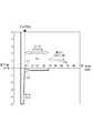
- FIG. 3is a diagram showing a measurement result of a change (mm) in displacement of the substrate over time (seconds) in the substrate cooling method of the present embodiment.
- the x-axisindicates the in-plane direction of the substrate
- the z-axisindicates the direction perpendicular to the substrate surface.
- the displacement amountis a displacement amount in the z-axis direction
- the displacement amount at the center of the substrate 200is defined as L1 (801 in FIG. 8) with reference to the upper surface of the substrate 200 (802 in FIG. 8).
- the displacement amount of the peripheral portion of the substrate 200is defined as L2 (801 in FIG. 8) with reference to the upper surface of the substrate 200 (802 in FIG. 8).
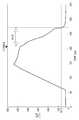
- FIG. 4shows a measurement result of a change (mm) in displacement of the substrate over time (seconds) in the direct contact type substrate cooling method of the comparative example in which the substrate is brought into direct contact with the cooling plate for cooling.
- the horizontal axisindicates a time axis of the substrate processing time indicating the passage of the entire time for processing the substrate, and a time axis of the substrate cooling time indicating the passage of time of the substrate cooling process.
- the substrate processing time of 110 secondscorresponds to the origin of the substrate cooling time axis, and cooling starts at this point.
- the amount of displacement of the substratewas measured using a laser displacement sensor that can measure the displacement of the measurement point of the substrate in a non-contact state.
- a solid line L1indicates the amount of displacement of the center of the substrate 200 (801 in FIG. 8) with reference to the upper surface of the substrate 200 (802 in FIG. 8).
- a broken line L2indicates the amount of displacement of the peripheral portion of the substrate 200 (801 in FIG. 8) with reference to the upper surface of the substrate 200 (802 in FIG. 8).
- a solid line L11indicates the amount of displacement of the center of the substrate 200 in the direct contact cooling method
- a broken line L12indicates the peripheral portion of the substrate 200. The amount of displacement is shown. Also, the time (seconds) shown on the horizontal axis in FIG.
- the time axis of the substrate cooling time in FIG. 4is set to 0 seconds starting from the time when each cooling process is started.
- the laser displacement sensor(not shown) is installed vertically above the substrate 200, the position in the vertical upward direction closer to the laser displacement sensor than the substrate mounting surface 211a of the cooling plate 211 is The negative direction on the vertical axis represents the displacement amount as a negative value.
- the sputtering apparatus of the embodimentwas used.
- a circular silicon substrate having a diameter of 300 mmwas used as the substrate 200.
- a position 5 mm inside from the outer peripheral edge of the substrate 200is set as a measurement point in the peripheral portion of the substrate 200. Note that although there are a plurality of measurement points in the peripheral portion of the substrate 200, for the sake of convenience, a value having the maximum displacement among the plurality of measurement points measured this time is described.
- the substrate 200 indicated by the solid line L11from the time when 15 seconds have elapsed from the start of cooling after the substrate contacts the cooling plate.
- Displacementbegins to occur in the central portion and the peripheral portion of the substrate 200 indicated by the broken line L12.
- substrate 200 and the displacement amount of a peripheral partwas 2.7 mm and 0.4 mm, respectively, and the maximum value of the difference was 2.3 mm.
- the displacement amountreturns to zero when 62 seconds have elapsed from the time when 15 seconds have elapsed since the start of cooling, that is, when 77 seconds have elapsed since the start of cooling.
- This amount of displacementis due to the fact that the substrate comes into contact with the substrate mounting surface 211a of the cooling plate and a temperature gradient is generated inside the substrate, causing the substrate to warp. As the substrate is warped, the substrate and the cooling plate are rubbed, causing generation of particles and a scratch on the back surface of the substrate.
- the transport positionis shifted from a predetermined position due to the warp of the substrate, causing a transport trouble such as a crack of the substrate. It becomes.
- the substrateshould not be carried out of the load lock chamber until the warpage of the substrate returns to zero.
- the residence time of the substrate in the load lock chamber 2 obtained from the experimental results regarding displacement shown in FIG. 3will be considered.
- the time from when the substrate cooling process is started until the substrate can be unloaded from the load lock chamber 2is defined as the staying time.
- the substrate displacementis zero, that is, the substrate warp is zero, and can be transported after the substrate cooling is started.
- the elapsed time until reaching a new statewas 77 seconds.
- the substrate cooling method of the present embodimentas shown in FIG. 3, during the first cooling step P1, the center portion of the substrate 200 indicated by the solid line L1 and the peripheral portion indicated by the broken line L2 are displaced.
- the differenceis 0.2 mm or less. This is presumably because the entire surface of the substrate is uniformly cooled by the cooling gas uniformly contacting the entire surface of the substrate 200.
- the difference in displacement generated in the central portion and the peripheral portion of the substrate 200is large for 10 seconds immediately after the first cooling step P1 is started. It is considered that this is not a difference in displacement due to the substrate cooling method but a difference in displacement due to heating of the film forming process in the processing chamber, that is, a warp of the substrate.
- the difference in displacement between the central portion and the peripheral portion of the substrateis 0.1 mm or less even during the second cooling step P2.
- the first cooling process P1causes the substrate 200 to directly contact the substrate mounting surface of the cooling plate 211 and cause a difference in displacement, that is, a substrate warp even if a temperature gradient occurs in the substrate 200. It is thought that this is because the temperature is cooled to a temperature that does not reach it.
- the displacement of the substrate generated during the first cooling process P1 and the second cooling process P2was 0.2 mm or less.
- the time during which the transfer operation is limited by the difference in displacement of the substrate, that is, the warpage of the substrate, that is, the residence time of the substrate in the load lock chamberwas 10 seconds.
- FIG. 5is a diagram illustrating an experimental result regarding a temperature change of the substrate 200 by the substrate cooling method of the embodiment.
- FIG. 6is a diagram illustrating an experimental result of a temperature change of the substrate by the direct contact type substrate cooling method of the comparative example in which the substrate 200 is directly brought into contact with the cooling plate 211 to be cooled.
- FIG. 5shows the relationship between the temperature change at the center point of the substrate 200 and time in the substrate cooling method of the embodiment.
- FIG. 6shows the relationship between the temperature change at the center point of the substrate 200 and time in the direct contact type substrate cooling method of the comparative example using the cooling plate.
- the temperature of the substrate 200was measured using a thermocouple.
- the temperaturecan be rapidly cooled and transported.
- the time required to reach 70 ° C.was 47 seconds.
- the substrate cooling method of the embodimentwill be considered. As shown in FIG. 5, in the substrate cooling method of the embodiment, when the temperature of the substrate is lowered to near 200 ° C., the temperature drop gradient becomes relatively gentle. Therefore, at this time, the temperature lowering gradient is increased again and the cooling time can be shortened by shifting to the second cooling step P2 in which the substrate is brought into contact with the substrate mounting surface of the cooling plate and cooled.
- the elapsed time from when the substrate 200 is placed on the substrate transfer pin 212 to the time when the temperature of the substrate 200 is reduced to 70 ° C., which is a temperature at which the substrate 200 can be carried out,is calculated as the substrate in the load lock chamber 2. Assuming 200 staying hours, the staying time was 64 seconds.
- the time during which the substrate 200 stays in the load lock chamber 2is a time until the difference in the displacement amount of the substrate, that is, the warpage of the substrate becomes zero and the substrate temperature becomes 70 ° C. or less at which the substrate can be transported. is there. From the respective measurement results relating to the displacement amount of the substrate shown in FIGS. 3 and 4 and the respective measurement results relating to the temperature shown in FIGS. 5 and 6, the time that can be conveyed in the direct contact type substrate cooling method of the comparative example using the cooling plate 211. Is 77 seconds when the displacement amount becomes zero.
- the time during which the substrate can be transferredis 64 seconds, which is the elapsed time until the substrate temperature reaches 70 ° C., which is equal to or less than the conventional one. Therefore, according to the cooling method of the present embodiment, in the substrate 200 to be cooled, the occurrence of substrate warpage can be suppressed and productivity is not reduced.
- the rear surface (lower surface) of the substrateis placed on the substrate placement surface 211a of the cooling plate 211 and cooled, but the present invention is not limited to this configuration. Any structure may be used as long as it is in contact with the cooling plate 211. That is, for example, a configuration in which the surface (upper surface) of the substrate is in contact with the substrate contact surface that is the lower surface of the cooling plate 211 may be employed.
- the semiconductor substrate 200is described as the substrate 200.
- the present inventioncan be similarly applied to other substrates such as a glass substrate for a flat panel display.
- FIG. 7is a diagram illustrating the configuration of the cooling chamber 21.
- the cooling gas introduction unit 218has a configuration in which vent gas (N 2 ) is introduced into the first cooling gas introduction valve 216 and the second cooling gas introduction valve 215, respectively.
- the vent gas introduction line 715is one system.
- the vent gas introduction line 715is connected to the mass flow controller 720 and the valve 730, and a cooling gas (vent gas (N 2 )) is introduced into the cooling chamber 21.
- the mass flow controller 720is connected to the sequencer 740.
- the sequencer 740is further connected to the encoder 750.
- the encoder 750can detect how far the substrate delivery pin 212 is from the substrate placement surface 211a of the substrate holder.
- Position information from the encoder 750is input to the sequencer 740.
- the sequencer 740controls the operation of the motor 760 based on this position information, and controls the vertical movement of the substrate transfer pin 212.
- the sequencer 740feeds back the position information of the encoder 750 to the mass flow controller 720.
- the mass flow controller 720introduces a cooling gas (vent gas (N 2 )) into the cooling chamber in accordance with the flow rate instruction information from the sequencer 740.
Landscapes
- Engineering & Computer Science (AREA)
- Chemical & Material Sciences (AREA)
- Microelectronics & Electronic Packaging (AREA)
- General Physics & Mathematics (AREA)
- Manufacturing & Machinery (AREA)
- Computer Hardware Design (AREA)
- Physics & Mathematics (AREA)
- Power Engineering (AREA)
- Condensed Matter Physics & Semiconductors (AREA)
- Chemical Kinetics & Catalysis (AREA)
- Materials Engineering (AREA)
- Mechanical Engineering (AREA)
- Metallurgy (AREA)
- Organic Chemistry (AREA)
- Container, Conveyance, Adherence, Positioning, Of Wafer (AREA)
Abstract
Description
Translated fromJapanese本発明は、基板処理装置が備えるロードロックチャンバにおいて、基板を冷却するための基板冷却方法及び半導体の製造方法に関する。The present invention relates to a substrate cooling method and a semiconductor manufacturing method for cooling a substrate in a load lock chamber provided in the substrate processing apparatus.
スパッタリング装置等の基板処理装置では、高温状態の処理チャンバ内で成膜処理が行われるため、基板が500℃以上の高温に加熱される。そして、この高温に加熱された基板は、処理チャンバに対して基板を搬送するためのロードロックチャンバを経由して、基板処理装置から搬出される。しかしながら、基板が高温状態のままで大気中に搬出されてしまうと、基板表面に自然酸化膜が形成され易くなる。基板表面に付着したパーティクルが自然酸化膜と化学反応し、基板に構成されたデバイスの欠陥になり易いという問題がある。さらに、このような場合には、高温状態の基板が、基板を収納するカセット等に接触することで熱変形させてしまう等の問題もある。このため、高温状態の基板を搬出可能な温度まで冷却した後に、基板処理装置から基板を搬出する必要がある。In a substrate processing apparatus such as a sputtering apparatus, since a film forming process is performed in a high temperature processing chamber, the substrate is heated to a high temperature of 500 ° C. or higher. Then, the substrate heated to this high temperature is unloaded from the substrate processing apparatus via a load lock chamber for transporting the substrate to the processing chamber. However, if the substrate is carried out into the atmosphere while being in a high temperature state, a natural oxide film is likely to be formed on the substrate surface. There is a problem that particles adhering to the surface of the substrate chemically react with the natural oxide film and easily cause defects in the device formed on the substrate. Further, in such a case, there is a problem that a substrate in a high temperature state is thermally deformed by contacting a cassette or the like that stores the substrate. For this reason, it is necessary to carry out the substrate from the substrate processing apparatus after cooling the substrate in a high temperature state to a temperature at which it can be carried out.
近年では、加熱された基板を冷却するために、ロードロックチャンバ内に基板を載置し、ロードロックチャンバ内に冷却ガスを供給することで、冷却ガスを媒体にして基板を間接的に冷却する冷却方法が用いられている(特許文献1の図4参照)。In recent years, in order to cool a heated substrate, the substrate is placed in a load lock chamber, and a cooling gas is supplied into the load lock chamber, thereby indirectly cooling the substrate using the cooling gas as a medium. A cooling method is used (see FIG. 4 of Patent Document 1).
また、他の基板冷却方法としては、低温に温度制御された冷却プレートをロードロックチャンバ内に配置し、加熱された基板を冷却プレートの基板載置面上に直接に載置し、冷却プレートによって基板を直接的に冷却する方法がある(特許文献2の図2参照)。As another substrate cooling method, a cooling plate whose temperature is controlled to a low temperature is disposed in the load lock chamber, and the heated substrate is placed directly on the substrate placement surface of the cooling plate. There is a method of directly cooling the substrate (see FIG. 2 of Patent Document 2).
しかしながら、特許文献1の冷却ガスによる間接的な冷却方法では、基板全面を均一に冷却することができるが、冷却時間が長くなり、ロードロックチャンバ内に基板が滞在する時間が増えるので、生産性の低下を招いていた。However, the indirect cooling method using the cooling gas of
また、特許文献2の冷却プレートによる直接的な冷却方法では、基板を急速に冷却することができるが、冷却プレートに接触している基板の裏面と、冷却プレートに接触していない基板の表面との間に基板の厚さ方向の熱勾配が発生する。この熱勾配が発生することで、基板に歪みが生じてしまう。この歪みによって生じる基板の反りが、基板と冷却ステージとが擦れる状態を招き、パーティクルの発生、基板の裏面への傷の発生、さらには、反った基板を搬送させたときに搬送の位置ずれが発生し、基板の割れ等の問題を引き起こしていた。Further, in the direct cooling method using the cooling plate of
一方で、特許文献1(図1及び図2参照)では、基板が収容される真空容器内の上下に上部冷却機構及び下部冷却機構がそれぞれ設けられた基板冷却装置、及び冷却方法が開示されている。この特許文献1では、冷却初期に、基板は上部冷却機構と下部冷却機構との間に保持され、冷却ガスによって基板の周囲から冷却される(間接冷却)。そして、冷却後期には、基板は下部冷却機構に近接させた位置に保持され、基板に近接させた下部冷却機構の冷却面の全面によって、基板は冷却される。On the other hand, Patent Document 1 (see FIGS. 1 and 2) discloses a substrate cooling apparatus and a cooling method in which an upper cooling mechanism and a lower cooling mechanism are respectively provided above and below a vacuum container in which a substrate is accommodated. Yes. In
上述したように、特許文献1においては、基板全体を冷却するので歪みが生じないが、冷却時間が長くなるため、生産性の低下を招く問題がある。また、特許文献2においては、基板の直接冷却を行っているので、基板の厚さ方向に対して熱勾配が発生してしまう。このため、特許文献2では、基板の歪みを抑制することが困難である。As described above, in
そこで、本発明は、上述した課題を解決し、冷却される基板に歪みが発生するのを抑制するとともに、基板を効率的に冷却することができる基板冷却方法を提供することを目的とする。Therefore, an object of the present invention is to solve the above-described problems, and to provide a substrate cooling method capable of efficiently suppressing the substrate while suppressing the occurrence of distortion in the substrate to be cooled.
上記の目的を達成する本発明にかかる基板冷却方法は、処理チャンバで加熱された基板を、前記基板との当接により前記基板を冷却する基板当接面を有する冷却プレートが配置されたロードロックチャンバに搬入した後、前記ロードロックチャンバに冷却ガスを供給して前記基板を冷却する基板冷却方法であって、
前記基板と前記冷却プレートの前記基板当接面との間に間隔をあけた状態で、前記基板の周囲に前記冷却ガスを供給して前記基板を冷却する第1の冷却工程と、
前記基板を前記冷却プレートの前記基板当接面に当接させて前記基板を前記冷却プレートによって冷却する第2の冷却工程と、を有することを特徴とする。A substrate cooling method according to the present invention that achieves the above object includes a load lock in which a cooling plate having a substrate contact surface that cools a substrate heated in a processing chamber by contacting the substrate is disposed. A substrate cooling method for cooling the substrate by supplying a cooling gas to the load lock chamber after being loaded into the chamber,
A first cooling step of cooling the substrate by supplying the cooling gas to the periphery of the substrate in a state where there is a gap between the substrate and the substrate contact surface of the cooling plate;
And a second cooling step of bringing the substrate into contact with the substrate contact surface of the cooling plate and cooling the substrate with the cooling plate.
上記の目的を達成する本発明にかかる半導体の製造方法は、基板との当接により前記基板を冷却する基板当接面を有する冷却プレートが配置されたロードロックチャンバと、前記基板に薄膜を形成する処理チャンバと、を有する半導体製造装置における半導体の製造方法であって、
前記基板を前記ロードロックチャンバから前記処理チャンバに搬入する搬入工程と、
前記処理チャンバに搬入された基板上に半導体の一部を構成する薄膜を形成する形成工程と、
前記薄膜が形成された基板をロードロックチャンバ内の冷却プレートに載置する載置工程と、
前記薄膜が形成された基板を前記処理チャンバから前記ロードロックチャンバに搬送し、前記基板と前記冷却プレートの前記基板当接面との間に間隔をあけた状態で、前記基板の周囲に冷却ガスを供給して前記基板を冷却する第1の冷却工程と、
前記基板を前記冷却プレートの前記基板当接面に当接させて前記基板を前記冷却プレートによって冷却することを特徴とする第2の冷却工程と、を有することを特徴とする。A semiconductor manufacturing method according to the present invention that achieves the above object includes a load lock chamber in which a cooling plate having a substrate contact surface for cooling the substrate by contact with the substrate is disposed, and a thin film formed on the substrate A semiconductor manufacturing method in a semiconductor manufacturing apparatus having a processing chamber,
A loading step of loading the substrate from the load lock chamber into the processing chamber;
Forming a thin film constituting a part of a semiconductor on a substrate carried into the processing chamber;
A placing step of placing the substrate on which the thin film is formed on a cooling plate in a load lock chamber;
The substrate on which the thin film is formed is transferred from the processing chamber to the load lock chamber, and a cooling gas is formed around the substrate in a state where a gap is provided between the substrate and the substrate contact surface of the cooling plate. A first cooling step for cooling the substrate by supplying
A second cooling step, wherein the substrate is brought into contact with the substrate contact surface of the cooling plate and the substrate is cooled by the cooling plate.
本発明によれば、冷却される基板に歪みが発生するのを抑制するとともに、基板を効率的に冷却することができるので、生産性を低下させずに、基板の歪みに伴う問題点を防ぐことができる。According to the present invention, it is possible to suppress the occurrence of distortion in the substrate to be cooled and to efficiently cool the substrate, thereby preventing problems associated with the distortion of the substrate without reducing productivity. be able to.
本発明のその他の特徴及び利点は、添付図面を参照とした以下の説明により明らかになるであろう。なお、添付図面においては、同じ若しくは同様の構成には、同じ参照番号を付す。Other features and advantages of the present invention will become apparent from the following description with reference to the accompanying drawings. In the accompanying drawings, the same or similar components are denoted by the same reference numerals.
添付図面は明細書に含まれ、その一部を構成し、本発明の実施の形態を示し、その記述と共に本発明の原理を説明するために用いられる。
以下、本発明の実施の形態について図面を参照して説明する。Hereinafter, embodiments of the present invention will be described with reference to the drawings.
図1は、ロードロックチャンバを備える実施形態のスパッタリング装置の構成を模式的に示す平面図である。FIG. 1 is a plan view schematically showing a configuration of a sputtering apparatus according to an embodiment including a load lock chamber.
本実施形態のスパッタリング装置は、いわゆるマルチチャンバタイプの装置であり、基板に所定の処理を行うための複数の処理チャンバ1と、これら処理チャンバ1に基板を搬入及び搬出するための2つのロードロックチャンバ2と、を備えている。また、このスパッタリング装置は、ロードロックチャンバ2及び複数の処理チャンバ1がそれぞれ接続されるコアチャンバ3を備えている。The sputtering apparatus of this embodiment is a so-called multi-chamber type apparatus, and includes a plurality of
コアチャンバ3とロードロックチャンバ2との間、及びコアチャンバ3と処理チャンバ1との間には、各チャンバを互いに連通させると共に気密に分離させるためのゲートバルブ(不図示)が開閉可能にそれぞれ設けられている。Between the
また、本実施形態では、2つのロードロックチャンバ2を備えることで、処理チャンバ1に対して基板の搬出、搬入を行う際に、2つのチャンバを交互に使い分けることによって、生産性の向上が図られている。Further, in the present embodiment, by providing two
本実施形態では複数の処理チャンバ1が設けられている。複数の処理チャンバ1は、全く同一の構成とされる場合もあるし、プロセスの内容に応じて異なった構成とされる場合もある。同一の構成は、一つの成膜工程を二つに分けて行うことでタクトタイムを短縮する場合等に採用される。また、異なる構成は、例えばチタンと窒化チタンとを積層するバリア膜の作成のように、異種薄膜を積層する場合等に採用される。In this embodiment, a plurality of
本実施形態のスパッタリング装置(図1)は、6つの処理チャンバ1を備えているが、処理チャンバ1の個数が6つに限定されるものではない。Although the sputtering apparatus (FIG. 1) of the present embodiment includes six
処理チャンバ1は、基板が載置される基板載置台と、この基板載置台に対向する位置に配置されたターゲット載置台と、このターゲット載置台に載置されるターゲットと、真空排気部、ガス導入部、電力供給部、等を備えている。なお、図1においてはこれらの構成の図示を省略する。The
詳細は後述するが、ロードロックチャンバ2には、基板が載置される基板載置台、真空排気部、基板加熱部、冷却ガス導入部、冷却プレート、基板受け渡しピンを上下駆動させるピン上下駆動機構、等を備えている。なお、図1においてはこれらの構成の図示を省略する。As will be described in detail later, the
コアチャンバ3には、コアチャンバ3の内部を排気するための真空排気部、複数の処理チャンバ1のそれぞれとコアチャンバ3との間で基板の搬送を行うための第1の基板搬送機構、等が設けられている。図1においてはこれらの図示を省略する。The
スパッタリング装置の大気側には、ロードロックチャンバ2と、ロードロックチャンバ2に対して基板の搬入、搬出を行うための第2の基板搬送機構(不図示)が設けられている。The atmosphere side of the sputtering apparatus is provided with a
次に、本実施形態のスパッタリング装置における特徴点をなすロードロックチャンバ2の構成について説明する。Next, the configuration of the
図2は、図1に示したスパッタリング装置のロードロックチャンバ2を模式的に示すA-A'断面図である。FIG. 2 is a cross-sectional view schematically showing the
図2に示すように、ロードロックチャンバ2の内部は、隔壁240を介して上下2室に区分されている。ロードロックチャンバ2は隔壁240の上部に配置された加熱チャンバ22と、隔壁240の下部に配置された冷却チャンバ21とを有している。As shown in FIG. 2, the interior of the
また、ロードロックチャンバ2とコアチャンバ3とは、ゲートバルブ231を介して連通されている。また、本実施形態では、ロードロックチャンバ2の内部が上下2室に区分されているので、ゲートバルブ231は、上部の加熱チャンバ22と下部の冷却チャンバ21とのそれぞれに1つずつ設けられている。なお、図2では、2つのゲートバルブを簡略化して1つのゲートバルブ231として模式的に示している。Further, the
加熱チャンバ22の上部には、大気側に配置された第2の基板搬送機構(不図示)によって搬入された基板200を所定の温度まで加熱するためのランプヒータ等の基板加熱部221が設けられている。また、加熱チャンバ22の下部には、第2の基板搬送機構またはコアチャンバ3内に設けられた第1の基板搬送機構との間で、基板200の受け渡しを行うための複数の基板受け渡しピン222が設けられている。A
冷却チャンバ21の下部には、処理チャンバ1で所定の成膜処理が施されて高温に加熱された基板200を所定の温度まで冷却するための冷却ガス導入部218が設けられている。また、冷却チャンバ21の上部には、所定の温度に調整された冷却プレート211が設けられている。この冷却プレート211の基板載置面211aの上には、大気側に配置された第2の基板搬送機構またはコアチャンバ3内に設けられた第1の基板搬送機構に対して基板200の受け渡しを行うための複数の基板受け渡しピン212が設けられている。A cooling
図2に示すように、冷却プレート211は、基板200が当接される基板当接面としての基板載置面211aを有している。また、冷却プレート211の内部には、冷媒を循環させるための冷媒用経路213が設けられており、冷媒温度調節部214によって冷媒の温度を調節することで、冷却プレート211の温度を所定の温度に制御することができる。なお、冷媒としては、熱伝達、温度保持、熱容量が比較的大きく、冷却用経路に対する腐食が比較的少なく、安価で、無毒な物質であればよく、例えば、純水を使用することができる。冷却プレート211の材料としては、基板を均一に冷却する観点から、例えば、熱伝導性が比較的高いアルミニウム、ステンレス、銅などを使用することができる。As shown in FIG. 2, the
また、加熱チャンバ22及び冷却チャンバ21の内部には、基板受け渡しピン222、212を上下方向に駆動させるピン上下駆動機構(不図示)が設けられている。ピン上下駆動機構は、基板受け渡しピン222、212を上昇させることで、第1及び第2の基板搬送機構に対して基板200の受け渡しを行うことが可能な状態にする。例えば、冷却チャンバ21において、基板受け渡しピン212が上昇した状態では、基板受け渡しピン212により基板200が支持された状態になる。基板受け渡しピン212により基板200が支持された状態で、第1及び第2の基板搬送機構に対して基板200は受け渡わたされる。Further, inside the
次に、図1及び図2を参照して、基板200に薄膜を成膜する動作について説明する。Next, the operation of forming a thin film on the
まず、基板200は、大気側に配置された第2の基板搬送機構によって、ロードロックチャンバ2の内部の加熱チャンバ22内に搬入される。このとき、基板200の受け渡しは、基板受け渡しピン222を介して行われる。First, the
続いて、真空排気部によって、加熱チャンバ22が真空排気された後、基板200は基板加熱部221によって所定の温度まで加熱される。基板200を加熱するのは、基板200内に含まれるガスを脱離させる(デガス)ためである。なお、真空処理する前に基板200を加熱する必要がない場合(基板200内に含まれるガスを脱離する必要がない場合)には、基板200が搬入された加熱チャンバ22が真空排気された後に、直ちに次の工程へ移行する。Subsequently, after the
次に、第1の基板搬送機構によって、基板200は加熱チャンバ22から処理チャンバ1内に搬入され、基板載置台に載置される。Next, the
続いて、真空排気部によって処理チャンバ1内が真空排気された後、ガス導入部によって、所望のガスが所定の流量に制御されて処理チャンバ1内に供給される。同時に、電力供給部によって、ターゲットに電力が供給され、処理チャンバ1内にプラズマ放電が発生し、ターゲットからスパッタされたスパッタ粒子が基板の表面に到達することによって、基板に薄膜が形成される。このとき、処理チャンバ1内で高温状態での成膜処理が行われるので、基板200は、例えば、500℃以上の高温に加熱される。Subsequently, after the inside of the
処理チャンバ1で所定の処理が施された基板200は、第1の基板搬送機構によって処理チャンバ1から搬出され、コアチャンバ3を介して、ロードロックチャンバ2の冷却チャンバ21の内部に搬入される。The
最後に、基板200は、冷却チャンバ2で冷却ガスによって冷却する第1の冷却工程と、冷却プレート211の基板載置面211aによって冷却する第2の冷却工程とを経て所定の温度まで冷却される。そして、基板200は、冷却された後に、大気側に配置された第2の基板搬送機構によって、スパッタリング装置の外部に搬出される。このとき、冷却チャンバ21に対する基板200の受け渡しは、基板受け渡しピン212によって行われる。Finally, the
このとき、冷却チャンバ2に供給される冷却ガスは、基板200を冷却するとともにロードロックチャンバ2を大気開放するためのベントガスとしても使用される。また、冷却ガスとしては、例えば窒素ガス、アルゴンガス、空気等が用いられる。At this time, the cooling gas supplied to the
次に、本実施形態におけるロードロックチャンバ2の冷却チャンバ21による冷却工程の詳細な処理について説明する。Next, detailed processing of the cooling process by the cooling
処理チャンバ1で所定の成膜処理が施された基板200は、第1の基板搬送機構によって、冷却チャンバ21の基板受け渡しピン212の上に載置される。そして、基板受け渡しピン212が移動されることによって、基板200の裏面と冷却プレート211の基板載置面211aとの間隔が0.2mm以上0.8mm以下、好ましくは0.5mmに調整される。The
そして、基板200の裏面と冷却プレート211の基板載置面211aとの間隔を、例えば、0.5mmに維持した状態で、第1の冷却ガス導入バルブ216を開き、冷却ガス流量制御部217によって、冷却ガスとしての窒素ガスを基板200の周囲に流量が制御された冷却ガスを供給する。これによって、基板200を窒素ガスで間接的に冷却する第1の冷却工程が行われる。このときに供給される窒素ガスの温度は、例えば、室温の25℃程度に設定されている。Then, with the distance between the back surface of the
なお、基板200と冷却プレート211との間隔は、0.8mm以下に設定されており、0.8mmよりも小さい方が望ましい。この理由は、間隔が0.8mmよりも小さい場合に、基板200と冷却プレート211との間の冷却ガスが、冷却プレート211によって冷却されるので、基板200の冷却効率を向上させる効果が得られるからである。In addition, the space | interval of the board |
しかし、基板200と冷却プレート211との間隔を極端に小さくし過ぎてしまった場合(例えば、0.2mmよりも小さい場合)には、基板200を冷却プレート211の基板載置面211aに直接に当接させた状態と、実質的に同じ状態になってしまい、基板200に歪みが発生してしまうので好ましくない。このため、基板200の歪みが発生しない間隔の範囲を予め実験等で見極めておくことが重要である。また、基板200と冷却プレート211との間隔が0.8mmよりも大きい場合には、冷却プレート211によって冷却ガスを冷却する効果が小さくなるので、好ましくない。従って、第1の冷却工程において基板200の冷却を行う場合に、ピン上下駆動機構は、予め、基板受け渡しピン212の上下移動を制御して、基板載置面211aと基板200の裏面とを、所定の間隔(0.2mm以上0.8mm以下、好ましくは0.5mm)に調整する。However, if the distance between the
第1の冷却工程は、冷却ガス流量制御部217により、第1の冷却ガスの流量制御を行う工程と、第2の冷却ガス導入バルブ215を開き、図示しない圧力検出部によって冷却チャンバ21内が大気圧になるまで流量を制御しないで直接、冷却ガスを供給する工程とを有する。In the first cooling process, the cooling gas flow
このように冷却ガスの流量を制御することによって、ロードロックチャンバ2内でのパーティクルの舞い上がりを効果的に防止することができる。By controlling the flow rate of the cooling gas in this way, it is possible to effectively prevent particles from rising in the
本実施形態おいて、第1の冷却工程における流量制御は、例えば、時間経過に伴って段階的(N段階(Nは2以上の自然数))に冷却ガスを増加させて供給することができる。各段階において供給する冷却ガスの流量や、流量を切り替えるタイミング(経過時間)、流量を切り替える段階の数は、適宜設定することが可能である。In the present embodiment, the flow rate control in the first cooling process can be performed by increasing the cooling gas in stages (N stages (N is a natural number of 2 or more)) with time, for example. The flow rate of the cooling gas supplied in each stage, the timing for switching the flow rate (elapsed time), and the number of stages for switching the flow rate can be set as appropriate.
第1の冷却工程に引き続いて、ピン上下駆動機構は、基板載置面211aと基板200の裏面とが当接する位置まで、基板受け渡しピン212を降下させる。基板200の裏面を冷却プレート212の基板載置面211aに当接させた状態で、第2の冷却工程が実行される。このとき、冷却プレート211は、冷媒温度調節部214によって所定の温度に冷却されており、基板200を良好に冷却することができる。Subsequent to the first cooling step, the pin vertical drive mechanism lowers the
第2の冷却工程が完了した後に、ピン上下駆動機構は、基板受け渡しピン212を上昇させて、基板載置面211aに対して基板200の裏面を離間した状態して保持する。そして、第2の基板搬送機構は、基板受け渡しピン212により支持されている基板200を受け取り、ロードロックチャンバ2内で冷却された基板200をスパッタリング装置の外部に搬出する。After the second cooling process is completed, the pin up / down drive mechanism raises the
図3は、本実施形態の基板冷却方法において、時間(秒)の経過に伴う基板の変位量の変化(mm)の測定結果を示す図である。図8において、x軸は基板の面内方向を示し、z軸は基板面に垂直な方向を示す。変位量とは、z軸方向の変位量であり、基板200の上面を基準とした(図8の802)、基板200の中心の変位量をL1とする(図8の801)。また、基板200の上面を基準とした(図8の802)、基板200の周辺部の変位量をL2とする(図8の801)。FIG. 3 is a diagram showing a measurement result of a change (mm) in displacement of the substrate over time (seconds) in the substrate cooling method of the present embodiment. In FIG. 8, the x-axis indicates the in-plane direction of the substrate, and the z-axis indicates the direction perpendicular to the substrate surface. The displacement amount is a displacement amount in the z-axis direction, and the displacement amount at the center of the
図4は、冷却プレートに基板を直接に当接させて冷却する、比較例の直接接触方式の基板冷却方法において、時間(秒)の経過に伴う基板の変位量の変化(mm)の測定結果を示す図である。図4では、横軸に、基板を処理する全体的な時間の経過を示す基板処理時間の時間軸と、基板の冷却処理の時間経過を示す基板冷却時間の時間軸と、が示されている。基板処理時間110秒の時点が基板冷却時間軸の原点に対応し、この時点で冷却開始となる。なお、基板の変位量は、非接触状態で基板の測定点の変位を測定することができるレーザ変位センサを使用して測定した。FIG. 4 shows a measurement result of a change (mm) in displacement of the substrate over time (seconds) in the direct contact type substrate cooling method of the comparative example in which the substrate is brought into direct contact with the cooling plate for cooling. FIG. In FIG. 4, the horizontal axis indicates a time axis of the substrate processing time indicating the passage of the entire time for processing the substrate, and a time axis of the substrate cooling time indicating the passage of time of the substrate cooling process. . The substrate processing time of 110 seconds corresponds to the origin of the substrate cooling time axis, and cooling starts at this point. The amount of displacement of the substrate was measured using a laser displacement sensor that can measure the displacement of the measurement point of the substrate in a non-contact state.
図3において、実線L1は、基板200の上面を基準とした(図8の802)、基板200の中心の変位量を示す(図8の801)。破線L2は、基板200の上面を基準とした(図8の802)、基板200の周辺部の変位量を示している(図8の801)。また、冷却プレート211による冷却の比較例として、実線L11(図4)は、直接接触方式の冷却方法における基板200の中心の変位量を示し、破線L12(図4)は、基板200の周辺部の変位量を示している。また、図3の横軸及び図4の基板冷却時間の時間軸に示す時間(秒)は、それぞれの冷却工程が開始された時点を起点として0秒に設定されている。なお、本実施形態では、レーザ変位センサ(不図示)が基板200の垂直上方に設置されているため、冷却プレート211の基板載置面211aよりもレーザ変位センサに近い垂直上方方向の位置を、縦軸における負の方向としており、変位量を負の値として示している。なお、測定では、実施形態のスパッタリング装置を使用した。In FIG. 3, a solid line L1 indicates the amount of displacement of the center of the substrate 200 (801 in FIG. 8) with reference to the upper surface of the substrate 200 (802 in FIG. 8). A broken line L2 indicates the amount of displacement of the peripheral portion of the substrate 200 (801 in FIG. 8) with reference to the upper surface of the substrate 200 (802 in FIG. 8). As a comparative example of cooling by the
このとき、基板200としては、直径300mmの円形状のシリコン基板を使用した。本実施形態では、基板200の外周縁部から5mm内側の位置を、基板200の周辺部における測定点とした。なお、基板200の周辺部には、複数の測定点が存在するが、便宜上、今回測定した複数の測定点のうちで、変位が最大の値を記載した。At this time, a circular silicon substrate having a diameter of 300 mm was used as the
図4に示すように、冷却プレート211による比較例の直接接触方式の基板冷却方法では、基板が冷却プレートに当接した後、冷却開始から15秒間が経過した時点から実線L11で示す基板200の中心部と、破線L12で示す基板200の周辺部と、に変位が生じ始める。そして、基板200の中心の変位量と周辺部の変位量との最大変位は、それぞれ2.7mm、0.4mmであり、その差の最大値は、2.3mmであった。そして、冷却開始から15秒間の経過時点から更に62秒間が経過した時点で、すなわち、冷却開始から77秒間が経過した時点で、変位量が零に戻っている。As shown in FIG. 4, in the direct contact type substrate cooling method of the comparative example using the
この変位量は、基板が冷却プレートの基板載置面211aに接触して基板内部に温度勾配が生じたことに起因しており、基板に反りを生じさせる。基板に反りが生じるのに伴って、基板と冷却プレートとの擦れを招き、パーティクルの発生や基板の裏面に擦り傷が生じる原因となる。This amount of displacement is due to the fact that the substrate comes into contact with the
また、反りが生じた状態の基板が第2の基板搬送機構によって搬送された場合には、基板の反りによって搬送位置が所定の位置からずれてしまい、基板の割れ等の搬送トラブルを発生させる原因となる。In addition, when a substrate in a warped state is transported by the second substrate transport mechanism, the transport position is shifted from a predetermined position due to the warp of the substrate, causing a transport trouble such as a crack of the substrate. It becomes.
したがって、基板の温度が所定の温度まで冷却された後も、基板の反りが零に戻るまでの時間は、基板をロードロックチャンバから搬出するべきではない。Therefore, even after the temperature of the substrate is cooled to a predetermined temperature, the substrate should not be carried out of the load lock chamber until the warpage of the substrate returns to zero.
そこで、図3に示す変位に関する実験結果から得られるロードロックチャンバ2における基板の滞在時間について考察する。本実施形態の基板冷却方法と比較するため、基板の冷却工程が開始された時点から、基板をロードロックチャンバ2から搬出可能になるまでの時間を滞在時間とする。Therefore, the residence time of the substrate in the
図4に示す変位に関する実験結果から、冷却プレートによる比較例の直接接触方式の基板冷却方法では、基板の冷却が開始されてから、基板の変位が零すなわち基盤の反りが零になって搬送可能な状態になるまでの経過時間は77秒間であった。From the experimental results relating to the displacement shown in FIG. 4, in the direct contact type substrate cooling method of the comparative example using the cooling plate, the substrate displacement is zero, that is, the substrate warp is zero, and can be transported after the substrate cooling is started. The elapsed time until reaching a new state was 77 seconds.
これに対して、本実施形態の基板冷却方法では、図3に示すように、第1の冷却工程P1の間において、実線L1で示す基板200の中心部と、破線L2で示す周辺部の変位の差異が0.2mm以下である。これは、冷却ガスが基板200の全面に均一に接触することによって、基板全面が均一に冷却されるためであると考えられる。ここで、基板200の中心部と周辺部において発生する変位の差異が大きいのは、第1の冷却工程P1が開始された直後の10秒間であることから、この変位の差異は、実施形態の基板冷却方法による変位の差異ではなく、処理チャンバで成膜処理の加熱による変位の差異すなわち基板の反りであると考えられる。そして、本実施形態の基板冷却方法によれば、第1の冷却工程P1が開始されてから10秒経過後に、基板200を搬送可能になると判断できる。On the other hand, in the substrate cooling method of the present embodiment, as shown in FIG. 3, during the first cooling step P1, the center portion of the
また、図3によれば、第2の冷却工程P2の間も、基板の中心部と周辺部における変位の差異は0.1mm以下である。これは、第1の冷却工程P1によって、基板200が冷却プレート211の基板載置面に直接に接触して、基板200に温度勾配が生じても変位の差異すなわち基板の反りを生じさせるには至らない温度まで冷却されているためであると考えられる。Further, according to FIG. 3, the difference in displacement between the central portion and the peripheral portion of the substrate is 0.1 mm or less even during the second cooling step P2. This is because the first cooling process P1 causes the
以上から実施形態の基板冷却方法では、第1の冷却工程P1及び第2の冷却工程P2中に生じる基板の変位は0.2mm以下であった。そして、基板の変位の差異すなわち基板の反りによって搬送動作が制限される時間、つまりロードロックチャンバにおける基板の滞在時間は10秒間であった。From the above, in the substrate cooling method of the embodiment, the displacement of the substrate generated during the first cooling process P1 and the second cooling process P2 was 0.2 mm or less. The time during which the transfer operation is limited by the difference in displacement of the substrate, that is, the warpage of the substrate, that is, the residence time of the substrate in the load lock chamber was 10 seconds.
図5は、実施形態の基板冷却方法による基板200の温度変化についての実験結果を示す図である。図6は、冷却プレート211に基板200を直接に接触させて冷却する、比較例の直接接触方式の基板冷却方法による基板の温度変化についての実験結果を示す図である。FIG. 5 is a diagram illustrating an experimental result regarding a temperature change of the
図5は、実施形態の基板冷却方法における基板200の中心点の温度変化と時間の関係を表している。また、図6は、冷却プレートによる比較例の直接接触方式の基板冷却方法における基板200の中心点の温度変化と時間の関係を表している。なお、基板200の温度は、熱電対を用いて測定した。FIG. 5 shows the relationship between the temperature change at the center point of the
冷却プレート211による比較例の直接接触方式の基板冷却方法では、図6に示すように、基板200が冷却プレート211の基板載置面211aに当接した後、急激に冷却され、搬送可能な温度70℃に達するのに要した時間が47秒間であった。In the direct contact type substrate cooling method of the comparative example using the
次に、実施形態の基板冷却方法に関して考察する。図5に示すように、実施形態の基板冷却方法では、基板の温度が200℃近くまで降温したときに、降温勾配が比較的緩やかになる。したがって、この時点で基板を冷却プレートの基板載置面に当接させて冷却する第2の冷却工程P2に移行させることで、再び降温勾配が高められ、冷却時間を短縮することができる。Next, the substrate cooling method of the embodiment will be considered. As shown in FIG. 5, in the substrate cooling method of the embodiment, when the temperature of the substrate is lowered to near 200 ° C., the temperature drop gradient becomes relatively gentle. Therefore, at this time, the temperature lowering gradient is increased again and the cooling time can be shortened by shifting to the second cooling step P2 in which the substrate is brought into contact with the substrate mounting surface of the cooling plate and cooled.
本実施形態によれば、基板200が基板受け渡しピン212に載置されてから、基板200の温度が搬出可能な温度である70℃まで低下した時間までの経過時間を、ロードロックチャンバ2における基板200の滞在時間とすると、滞在時間は64秒間であった。According to the present embodiment, the elapsed time from when the
ここで、基板200がロードロックチャンバ2の内部に滞在する時間は、基板の変位量の差異すなわち基板の反りが零になり、かつ基板の温度が搬送可能な70℃以下になるまでの時間である。図3及び図4に示す基板の変位量に関する各測定結果と図5及び図6に示す温度に関する各測定結果から、冷却プレート211による比較例の直接接触方式の基板冷却方法では搬送可能になる時間は変位量が零となる77秒間である。これに対して、本実施形態の基板冷却方法では、搬送可能になる時間は基板温度が70℃になるまでの経過時間である64秒間となり、従来と同等以下であった。したがって、本実施形態の冷却方法によれば、冷却される基板200において、基板の反りの発生を抑制することができるとともに、生産性の低下を招くことはない。Here, the time during which the
なお、本実施形態では、基板の裏面(下面)が冷却プレート211の基板載置面211aに載置されて冷却される構成が採られたが、この構成に限定されるものではなく、基板200が冷却プレート211に当接される構成であればよい。つまり、例えば、基板の表面(上面)が冷却プレート211の下面である基板当接面に当接される構成が採られてもよい。In the present embodiment, the rear surface (lower surface) of the substrate is placed on the
また、本実施形態では、基板200として、半導体用のシリコン基板を挙げて説明したが、フラットパネルディスプレイ用のガラス基板等の他の基板にも同様に適用できることは明らかである。In this embodiment, the
図7は、冷却チャンバ21の構成を例示した図である。尚、図2では、冷却ガス導入部218には、第1の冷却ガス導入バルブ216と第2の冷却ガス導入バルブ215にそれぞれベントガス(N2)が導入する構成となっていた。図7では、ベントガス導入ライン715は1系統である。ベントガス導入ライン715はマスフローコントローラ720とバルブ730とに接続され、冷却チャンバ21内に冷却ガス(ベントガス(N2))が導入される。マスフローコントローラ720はシーケンサ740に接続されている。シーケンサ740は更にエンコーダ750に接続されている。エンコーダ750は、基板受け渡しピン212が基板ホルダの基板載置面211aからどの程度間隔があいているか検知することが可能である。エンコーダ750からの位置情報はシーケンサ740に入力される。シーケンサ740は、この位置情報に基づきモータ760の動作制御を行い、基板受け渡しピン212の上下移動を制御する。また、シーケンサ740は、エンコーダ750の位置情報をマスフローコントローラ720にフィードバックする。マスフローコントローラ720は、シーケンサ740からの流量指示情報に従い、冷却チャンバ内に冷却ガス(ベントガス(N2))を導入する。FIG. 7 is a diagram illustrating the configuration of the cooling
本発明は上記実施の形態に制限されるものではなく、本発明の精神及び範囲から離脱することなく、様々な変更及び変形が可能である。従って、本発明の範囲を公にするために、以下の請求項を添付する。The present invention is not limited to the above embodiment, and various changes and modifications can be made without departing from the spirit and scope of the present invention. Therefore, in order to make the scope of the present invention public, the following claims are attached.
本願は、2008年9月4日提出の日本国特許出願特願2008-227006、2009年6月25日提出の日本国特許出願特願2009-151518、2009年7月22日提出の米国特許出願12/507,362を基礎として優先権を主張するものであり、その記載内容の全てを、ここに援用する。This application is Japanese Patent Application Japanese Patent Application No. 2008-227006 filed on September 4, 2008, Japanese Patent Application Japanese Patent Application No. 2009-151518 filed on June 25, 2009, and US Patent Application filed on July 22, 2009. No. 12 / 507,362 is claimed as the basis, and all of the description is incorporated herein.
Claims (7)
Translated fromJapanese前記基板と前記冷却プレートの前記基板当接面との間に間隔をあけた状態で、前記基板の周囲に前記冷却ガスを供給して前記基板を冷却する第1の冷却工程と、
前記基板を前記冷却プレートの前記基板当接面に当接させて前記基板を前記冷却プレートによって冷却する第2の冷却工程と、
を有することを特徴とする基板冷却方法。The substrate heated in the processing chamber is carried into a load lock chamber having a cooling plate having a substrate contact surface for cooling the substrate by contact with the substrate, and then a cooling gas is supplied to the load lock chamber. A substrate cooling method for cooling the substrate,
A first cooling step of cooling the substrate by supplying the cooling gas to the periphery of the substrate in a state where there is a gap between the substrate and the substrate contact surface of the cooling plate;
A second cooling step of bringing the substrate into contact with the substrate contact surface of the cooling plate and cooling the substrate by the cooling plate;
A method for cooling a substrate, comprising:
前記基板を前記ロードロックチャンバから前記処理チャンバに搬入する搬入工程と、
前記処理チャンバに搬入された基板上に半導体の一部を構成する薄膜を形成する形成工程と、
前記薄膜が形成された基板をロードロックチャンバ内の冷却プレートに載置する載置工程と、
前記薄膜が形成された基板を前記処理チャンバから前記ロードロックチャンバに搬送し、前記基板と前記冷却プレートの前記基板当接面との間に間隔をあけた状態で、前記基板の周囲に冷却ガスを供給して前記基板を冷却する第1の冷却工程と、
前記基板を前記冷却プレートの前記基板当接面に当接させて前記基板を前記冷却プレートによって冷却することを特徴とする第2の冷却工程と、
を有することを特徴とする半導体の製造方法。A semiconductor manufacturing method in a semiconductor manufacturing apparatus, comprising: a load lock chamber in which a cooling plate having a substrate contact surface for cooling the substrate by contact with the substrate is disposed; and a processing chamber for forming a thin film on the substrate There,
A loading step of loading the substrate from the load lock chamber into the processing chamber;
Forming a thin film constituting a part of a semiconductor on a substrate carried into the processing chamber;
A placing step of placing the substrate on which the thin film is formed on a cooling plate in a load lock chamber;
The substrate on which the thin film is formed is transferred from the processing chamber to the load lock chamber, and a cooling gas is provided around the substrate in a state where there is a gap between the substrate and the substrate contact surface of the cooling plate A first cooling step for cooling the substrate by supplying
A second cooling step, wherein the substrate is brought into contact with the substrate contact surface of the cooling plate and the substrate is cooled by the cooling plate;
A method for producing a semiconductor, comprising:
Applications Claiming Priority (6)
| Application Number | Priority Date | Filing Date | Title |
|---|---|---|---|
| JP2008227006 | 2008-09-04 | ||
| JP2008-227006 | 2008-09-04 | ||
| JP2009-151518 | 2009-06-25 | ||
| JP2009151518 | 2009-06-25 | ||
| US50736209A | 2009-07-22 | 2009-07-22 | |
| US12/507,362 | 2009-07-22 |
Publications (1)
| Publication Number | Publication Date |
|---|---|
| WO2010026772A1true WO2010026772A1 (en) | 2010-03-11 |
Family
ID=41796951
Family Applications (1)
| Application Number | Title | Priority Date | Filing Date |
|---|---|---|---|
| PCT/JP2009/004400CeasedWO2010026772A1 (en) | 2008-09-04 | 2009-09-04 | Substrate cooling method and semiconductor manufacturing method |
Country Status (1)
| Country | Link |
|---|---|
| WO (1) | WO2010026772A1 (en) |
Cited By (7)
| Publication number | Priority date | Publication date | Assignee | Title |
|---|---|---|---|---|
| CN103981504A (en)* | 2014-06-03 | 2014-08-13 | 上海先进半导体制造股份有限公司 | Physical vapor deposition machine table and cooling cavity thereof |
| JP2015008249A (en)* | 2013-06-26 | 2015-01-15 | 東京エレクトロン株式会社 | Temperature control method and plasma processing device |
| JP2015515742A (en)* | 2012-02-29 | 2015-05-28 | アプライド マテリアルズ インコーポレイテッドApplied Materials,Incorporated | Detoxification and stripping chamber in load lock configuration |
| JP2017168613A (en)* | 2016-03-16 | 2017-09-21 | 信越半導体株式会社 | Heat treatment apparatus |
| CN112095078A (en)* | 2020-09-24 | 2020-12-18 | 福建华佳彩有限公司 | Cooling buffer chamber for surface evaporation source and driving method |
| CN113025987A (en)* | 2019-12-09 | 2021-06-25 | 天虹科技股份有限公司 | Method and apparatus for reducing surface oxide formation of aluminum nitride |
| US20220310420A1 (en)* | 2021-03-25 | 2022-09-29 | Kokusai Electric Corporation | Cooling method, a method of manufacturing a semiconductor device and a non-transitory computer-readable recording medium |
Citations (6)
| Publication number | Priority date | Publication date | Assignee | Title |
|---|---|---|---|---|
| JPH0230128A (en)* | 1988-05-18 | 1990-01-31 | Veeco Instr Inc | Method of transferring and cooling substrate and apparatus for executing the method |
| JPH10107126A (en)* | 1996-09-17 | 1998-04-24 | Applied Materials Inc | Cooling chamber and method of operating the cooling chamber |
| JPH11102904A (en)* | 1997-09-25 | 1999-04-13 | Tokyo Electron Ltd | Substrate-cooling equipment |
| JP2001196363A (en)* | 1999-09-15 | 2001-07-19 | Applied Materials Inc | Method and apparatus for heating and cooling a substrate |
| JP2004221197A (en)* | 2003-01-10 | 2004-08-05 | Tokyo Electron Ltd | Treatment equipment |
| JP2008103707A (en)* | 2006-09-22 | 2008-05-01 | Hitachi Kokusai Electric Inc | Substrate processing apparatus and semiconductor device manufacturing method |
- 2009
- 2009-09-04WOPCT/JP2009/004400patent/WO2010026772A1/ennot_activeCeased
Patent Citations (6)
| Publication number | Priority date | Publication date | Assignee | Title |
|---|---|---|---|---|
| JPH0230128A (en)* | 1988-05-18 | 1990-01-31 | Veeco Instr Inc | Method of transferring and cooling substrate and apparatus for executing the method |
| JPH10107126A (en)* | 1996-09-17 | 1998-04-24 | Applied Materials Inc | Cooling chamber and method of operating the cooling chamber |
| JPH11102904A (en)* | 1997-09-25 | 1999-04-13 | Tokyo Electron Ltd | Substrate-cooling equipment |
| JP2001196363A (en)* | 1999-09-15 | 2001-07-19 | Applied Materials Inc | Method and apparatus for heating and cooling a substrate |
| JP2004221197A (en)* | 2003-01-10 | 2004-08-05 | Tokyo Electron Ltd | Treatment equipment |
| JP2008103707A (en)* | 2006-09-22 | 2008-05-01 | Hitachi Kokusai Electric Inc | Substrate processing apparatus and semiconductor device manufacturing method |
Cited By (10)
| Publication number | Priority date | Publication date | Assignee | Title |
|---|---|---|---|---|
| JP2015515742A (en)* | 2012-02-29 | 2015-05-28 | アプライド マテリアルズ インコーポレイテッドApplied Materials,Incorporated | Detoxification and stripping chamber in load lock configuration |
| JP2015008249A (en)* | 2013-06-26 | 2015-01-15 | 東京エレクトロン株式会社 | Temperature control method and plasma processing device |
| US10217616B2 (en) | 2013-06-26 | 2019-02-26 | Tokyo Electron Limited | Method of controlling temperature and plasma processing apparatus |
| CN103981504A (en)* | 2014-06-03 | 2014-08-13 | 上海先进半导体制造股份有限公司 | Physical vapor deposition machine table and cooling cavity thereof |
| JP2017168613A (en)* | 2016-03-16 | 2017-09-21 | 信越半導体株式会社 | Heat treatment apparatus |
| CN113025987A (en)* | 2019-12-09 | 2021-06-25 | 天虹科技股份有限公司 | Method and apparatus for reducing surface oxide formation of aluminum nitride |
| CN113025987B (en)* | 2019-12-09 | 2023-02-28 | 天虹科技股份有限公司 | Method for reducing surface oxide formation of aluminum nitride |
| CN112095078A (en)* | 2020-09-24 | 2020-12-18 | 福建华佳彩有限公司 | Cooling buffer chamber for surface evaporation source and driving method |
| CN112095078B (en)* | 2020-09-24 | 2023-12-05 | 福建华佳彩有限公司 | Cooling buffer chamber for surface evaporation source and driving method |
| US20220310420A1 (en)* | 2021-03-25 | 2022-09-29 | Kokusai Electric Corporation | Cooling method, a method of manufacturing a semiconductor device and a non-transitory computer-readable recording medium |
Similar Documents
| Publication | Publication Date | Title |
|---|---|---|
| JP4860167B2 (en) | Load lock device, processing system, and processing method | |
| WO2010026772A1 (en) | Substrate cooling method and semiconductor manufacturing method | |
| US9589819B1 (en) | Substrate processing apparatus | |
| JP6246961B2 (en) | Deposition equipment | |
| JP4761326B2 (en) | Thin film forming apparatus system and thin film forming method | |
| KR100639071B1 (en) | Thin-film deposition system | |
| CN111095517B (en) | Substrate processing apparatus, method for manufacturing semiconductor device, and storage medium | |
| JP2019062194A (en) | Substrate processing apparatus, method of manufacturing semiconductor device, and program | |
| CN111052336A (en) | Substrate processing apparatus, method of manufacturing semiconductor device, and program | |
| KR20110028250A (en) | Temperature-lowering method of substrate placement, computer readable storage media, and substrate processing system | |
| TW201724393A (en) | Substrate processing apparatus | |
| US7652227B2 (en) | Heating and cooling plate for a vacuum chamber | |
| JP4695297B2 (en) | Thin film forming apparatus and load lock chamber | |
| JP2007035874A (en) | Vacuum processing system | |
| JP2012195427A (en) | Substrate processing apparatus and substrate processing method | |
| US20080199610A1 (en) | Substrate processing apparatus, and substrate processing method | |
| KR101841980B1 (en) | Film forming apparatus | |
| US10115611B2 (en) | Substrate cooling method, substrate transfer method, and load-lock mechanism | |
| KR102515863B1 (en) | vacuum processing unit | |
| JPH11204443A (en) | Single wafer heat treatment device | |
| JP2006054282A (en) | Vacuum processing apparatus and wafer temperature recovery method | |
| JP4503713B2 (en) | Substrate cooling method for vacuum film formation | |
| KR20250125259A (en) | Substrate processing apparatus, substrate processing method, method of manufacturing semiconductor device and program | |
| WO2024029126A1 (en) | Substrate processing device, method for manufacturing semiconductor device, and program | |
| JP2010001550A (en) | Thin film deposition method |
Legal Events
| Date | Code | Title | Description |
|---|---|---|---|
| 121 | Ep: the epo has been informed by wipo that ep was designated in this application | Ref document number:09811302 Country of ref document:EP Kind code of ref document:A1 | |
| NENP | Non-entry into the national phase | Ref country code:DE | |
| 122 | Ep: pct application non-entry in european phase | Ref document number:09811302 Country of ref document:EP Kind code of ref document:A1 | |
| NENP | Non-entry into the national phase | Ref country code:JP |