WO2009119500A1 - Gas feeding device, treating device, treating method, and storage medium - Google Patents
Gas feeding device, treating device, treating method, and storage mediumDownload PDFInfo
- Publication number
- WO2009119500A1 WO2009119500A1PCT/JP2009/055658JP2009055658WWO2009119500A1WO 2009119500 A1WO2009119500 A1WO 2009119500A1JP 2009055658 WJP2009055658 WJP 2009055658WWO 2009119500 A1WO2009119500 A1WO 2009119500A1
- Authority
- WO
- WIPO (PCT)
- Prior art keywords
- gas
- flow space
- gas flow
- supply device
- gas supply
- Prior art date
Links
- 238000000034methodMethods0.000titleclaimsdescription59
- 238000003860storageMethods0.000titleclaimsdescription9
- 239000007789gasSubstances0.000claimsabstractdescription801
- 238000005192partitionMethods0.000claimsabstractdescription106
- 238000012545processingMethods0.000claimsdescription117
- 230000008569processEffects0.000claimsdescription56
- 239000000758substrateSubstances0.000claimsdescription42
- 238000010926purgeMethods0.000claimsdescription40
- 238000011144upstream manufacturingMethods0.000claimsdescription18
- 230000002093peripheral effectEffects0.000claimsdescription14
- 238000003672processing methodMethods0.000claimsdescription8
- 239000007795chemical reaction productSubstances0.000claimsdescription7
- 239000010409thin filmSubstances0.000claimsdescription5
- 239000011261inert gasSubstances0.000claimsdescription4
- 238000000638solvent extractionMethods0.000claimsdescription4
- 238000004590computer programMethods0.000claimsdescription2
- 238000010030laminatingMethods0.000claimsdescription2
- 239000010408filmSubstances0.000description33
- 239000010936titaniumSubstances0.000description27
- CBENFWSGALASAD-UHFFFAOYSA-NOzoneChemical compound[O-][O+]=OCBENFWSGALASAD-UHFFFAOYSA-N0.000description22
- 238000004088simulationMethods0.000description19
- 238000011156evaluationMethods0.000description16
- 238000012360testing methodMethods0.000description16
- 238000009826distributionMethods0.000description15
- 238000000231atomic layer depositionMethods0.000description13
- 238000012986modificationMethods0.000description10
- 230000004048modificationEffects0.000description10
- YXFVVABEGXRONW-UHFFFAOYSA-NTolueneChemical compoundCC1=CC=CC=C1YXFVVABEGXRONW-UHFFFAOYSA-N0.000description9
- 239000002994raw materialSubstances0.000description9
- 239000000463materialSubstances0.000description8
- 230000015572biosynthetic processEffects0.000description6
- 238000004519manufacturing processMethods0.000description5
- 230000007246mechanismEffects0.000description5
- 239000000203mixtureSubstances0.000description5
- 238000012546transferMethods0.000description5
- XAGFODPZIPBFFR-UHFFFAOYSA-NaluminiumChemical compound[Al]XAGFODPZIPBFFR-UHFFFAOYSA-N0.000description4
- 229910052782aluminiumInorganic materials0.000description4
- 238000005229chemical vapour depositionMethods0.000description4
- 238000009792diffusion processMethods0.000description4
- 230000000694effectsEffects0.000description4
- 229910004356Ti RawInorganic materials0.000description3
- 239000000919ceramicSubstances0.000description3
- XKRFYHLGVUSROY-UHFFFAOYSA-NArgonChemical compound[Ar]XKRFYHLGVUSROY-UHFFFAOYSA-N0.000description2
- 230000008901benefitEffects0.000description2
- 238000010586diagramMethods0.000description2
- 230000012447hatchingEffects0.000description2
- 125000003253isopropoxy groupChemical group[H]C([H])([H])C([H])(O*)C([H])([H])[H]0.000description2
- 239000002052molecular layerSubstances0.000description2
- 239000002245particleSubstances0.000description2
- 238000001020plasma etchingMethods0.000description2
- 239000004065semiconductorSubstances0.000description2
- 238000001179sorption measurementMethods0.000description2
- 229910052712strontiumInorganic materials0.000description2
- CIOAGBVUUVVLOB-UHFFFAOYSA-Nstrontium atomChemical compound[Sr]CIOAGBVUUVVLOB-UHFFFAOYSA-N0.000description2
- VXUYXOFXAQZZMF-UHFFFAOYSA-Ntitanium(IV) isopropoxideChemical compoundCC(C)O[Ti](OC(C)C)(OC(C)C)OC(C)CVXUYXOFXAQZZMF-UHFFFAOYSA-N0.000description2
- 239000006200vaporizerSubstances0.000description2
- KWOKXTAYEOWZSA-UHFFFAOYSA-NCC1=C(C(=C(C1([Sr])C)C)C)CChemical compoundCC1=C(C(=C(C1([Sr])C)C)C)CKWOKXTAYEOWZSA-UHFFFAOYSA-N0.000description1
- 229910002367SrTiOInorganic materials0.000description1
- RTAQQCXQSZGOHL-UHFFFAOYSA-NTitaniumChemical compound[Ti]RTAQQCXQSZGOHL-UHFFFAOYSA-N0.000description1
- 229910052786argonInorganic materials0.000description1
- 150000001875compoundsChemical class0.000description1
- 238000005094computer simulationMethods0.000description1
- 238000011109contaminationMethods0.000description1
- 230000003247decreasing effectEffects0.000description1
- 239000003989dielectric materialSubstances0.000description1
- 238000005530etchingMethods0.000description1
- 239000011521glassSubstances0.000description1
- 230000006872improvementEffects0.000description1
- 239000007788liquidSubstances0.000description1
- 230000001590oxidative effectEffects0.000description1
- JTQPTNQXCUMDRK-UHFFFAOYSA-Npropan-2-olate;titanium(2+)Chemical compoundCC(C)O[Ti]OC(C)CJTQPTNQXCUMDRK-UHFFFAOYSA-N0.000description1
- 238000004904shorteningMethods0.000description1
- VEALVRVVWBQVSL-UHFFFAOYSA-Nstrontium titanateChemical compound[Sr+2].[O-][Ti]([O-])=OVEALVRVVWBQVSL-UHFFFAOYSA-N0.000description1
- 229910052719titaniumInorganic materials0.000description1
- 238000009827uniform distributionMethods0.000description1
- 238000001947vapour-phase growthMethods0.000description1
Images


Classifications
- C—CHEMISTRY; METALLURGY
- C23—COATING METALLIC MATERIAL; COATING MATERIAL WITH METALLIC MATERIAL; CHEMICAL SURFACE TREATMENT; DIFFUSION TREATMENT OF METALLIC MATERIAL; COATING BY VACUUM EVAPORATION, BY SPUTTERING, BY ION IMPLANTATION OR BY CHEMICAL VAPOUR DEPOSITION, IN GENERAL; INHIBITING CORROSION OF METALLIC MATERIAL OR INCRUSTATION IN GENERAL
- C23C—COATING METALLIC MATERIAL; COATING MATERIAL WITH METALLIC MATERIAL; SURFACE TREATMENT OF METALLIC MATERIAL BY DIFFUSION INTO THE SURFACE, BY CHEMICAL CONVERSION OR SUBSTITUTION; COATING BY VACUUM EVAPORATION, BY SPUTTERING, BY ION IMPLANTATION OR BY CHEMICAL VAPOUR DEPOSITION, IN GENERAL
- C23C16/00—Chemical coating by decomposition of gaseous compounds, without leaving reaction products of surface material in the coating, i.e. chemical vapour deposition [CVD] processes
- C23C16/44—Chemical coating by decomposition of gaseous compounds, without leaving reaction products of surface material in the coating, i.e. chemical vapour deposition [CVD] processes characterised by the method of coating
- C23C16/455—Chemical coating by decomposition of gaseous compounds, without leaving reaction products of surface material in the coating, i.e. chemical vapour deposition [CVD] processes characterised by the method of coating characterised by the method used for introducing gases into reaction chamber or for modifying gas flows in reaction chamber
- C23C16/45563—Gas nozzles
- C23C16/45565—Shower nozzles
- C—CHEMISTRY; METALLURGY
- C23—COATING METALLIC MATERIAL; COATING MATERIAL WITH METALLIC MATERIAL; CHEMICAL SURFACE TREATMENT; DIFFUSION TREATMENT OF METALLIC MATERIAL; COATING BY VACUUM EVAPORATION, BY SPUTTERING, BY ION IMPLANTATION OR BY CHEMICAL VAPOUR DEPOSITION, IN GENERAL; INHIBITING CORROSION OF METALLIC MATERIAL OR INCRUSTATION IN GENERAL
- C23C—COATING METALLIC MATERIAL; COATING MATERIAL WITH METALLIC MATERIAL; SURFACE TREATMENT OF METALLIC MATERIAL BY DIFFUSION INTO THE SURFACE, BY CHEMICAL CONVERSION OR SUBSTITUTION; COATING BY VACUUM EVAPORATION, BY SPUTTERING, BY ION IMPLANTATION OR BY CHEMICAL VAPOUR DEPOSITION, IN GENERAL
- C23C16/00—Chemical coating by decomposition of gaseous compounds, without leaving reaction products of surface material in the coating, i.e. chemical vapour deposition [CVD] processes
- C23C16/22—Chemical coating by decomposition of gaseous compounds, without leaving reaction products of surface material in the coating, i.e. chemical vapour deposition [CVD] processes characterised by the deposition of inorganic material, other than metallic material
- C23C16/30—Deposition of compounds, mixtures or solid solutions, e.g. borides, carbides, nitrides
- C23C16/40—Oxides
- C23C16/409—Oxides of the type ABO3 with A representing alkali, alkaline earth metal or lead and B representing a refractory metal, nickel, scandium or a lanthanide
- C—CHEMISTRY; METALLURGY
- C23—COATING METALLIC MATERIAL; COATING MATERIAL WITH METALLIC MATERIAL; CHEMICAL SURFACE TREATMENT; DIFFUSION TREATMENT OF METALLIC MATERIAL; COATING BY VACUUM EVAPORATION, BY SPUTTERING, BY ION IMPLANTATION OR BY CHEMICAL VAPOUR DEPOSITION, IN GENERAL; INHIBITING CORROSION OF METALLIC MATERIAL OR INCRUSTATION IN GENERAL
- C23C—COATING METALLIC MATERIAL; COATING MATERIAL WITH METALLIC MATERIAL; SURFACE TREATMENT OF METALLIC MATERIAL BY DIFFUSION INTO THE SURFACE, BY CHEMICAL CONVERSION OR SUBSTITUTION; COATING BY VACUUM EVAPORATION, BY SPUTTERING, BY ION IMPLANTATION OR BY CHEMICAL VAPOUR DEPOSITION, IN GENERAL
- C23C16/00—Chemical coating by decomposition of gaseous compounds, without leaving reaction products of surface material in the coating, i.e. chemical vapour deposition [CVD] processes
- C23C16/44—Chemical coating by decomposition of gaseous compounds, without leaving reaction products of surface material in the coating, i.e. chemical vapour deposition [CVD] processes characterised by the method of coating
- C23C16/455—Chemical coating by decomposition of gaseous compounds, without leaving reaction products of surface material in the coating, i.e. chemical vapour deposition [CVD] processes characterised by the method of coating characterised by the method used for introducing gases into reaction chamber or for modifying gas flows in reaction chamber
- C23C16/45523—Pulsed gas flow or change of composition over time
- C23C16/45525—Atomic layer deposition [ALD]
- C23C16/45527—Atomic layer deposition [ALD] characterized by the ALD cycle, e.g. different flows or temperatures during half-reactions, unusual pulsing sequence, use of precursor mixtures or auxiliary reactants or activations
- C23C16/45531—Atomic layer deposition [ALD] characterized by the ALD cycle, e.g. different flows or temperatures during half-reactions, unusual pulsing sequence, use of precursor mixtures or auxiliary reactants or activations specially adapted for making ternary or higher compositions
- C—CHEMISTRY; METALLURGY
- C23—COATING METALLIC MATERIAL; COATING MATERIAL WITH METALLIC MATERIAL; CHEMICAL SURFACE TREATMENT; DIFFUSION TREATMENT OF METALLIC MATERIAL; COATING BY VACUUM EVAPORATION, BY SPUTTERING, BY ION IMPLANTATION OR BY CHEMICAL VAPOUR DEPOSITION, IN GENERAL; INHIBITING CORROSION OF METALLIC MATERIAL OR INCRUSTATION IN GENERAL
- C23C—COATING METALLIC MATERIAL; COATING MATERIAL WITH METALLIC MATERIAL; SURFACE TREATMENT OF METALLIC MATERIAL BY DIFFUSION INTO THE SURFACE, BY CHEMICAL CONVERSION OR SUBSTITUTION; COATING BY VACUUM EVAPORATION, BY SPUTTERING, BY ION IMPLANTATION OR BY CHEMICAL VAPOUR DEPOSITION, IN GENERAL
- C23C16/00—Chemical coating by decomposition of gaseous compounds, without leaving reaction products of surface material in the coating, i.e. chemical vapour deposition [CVD] processes
- C23C16/44—Chemical coating by decomposition of gaseous compounds, without leaving reaction products of surface material in the coating, i.e. chemical vapour deposition [CVD] processes characterised by the method of coating
- C23C16/455—Chemical coating by decomposition of gaseous compounds, without leaving reaction products of surface material in the coating, i.e. chemical vapour deposition [CVD] processes characterised by the method of coating characterised by the method used for introducing gases into reaction chamber or for modifying gas flows in reaction chamber
- C23C16/45582—Expansion of gas before it reaches the substrate
- C—CHEMISTRY; METALLURGY
- C23—COATING METALLIC MATERIAL; COATING MATERIAL WITH METALLIC MATERIAL; CHEMICAL SURFACE TREATMENT; DIFFUSION TREATMENT OF METALLIC MATERIAL; COATING BY VACUUM EVAPORATION, BY SPUTTERING, BY ION IMPLANTATION OR BY CHEMICAL VAPOUR DEPOSITION, IN GENERAL; INHIBITING CORROSION OF METALLIC MATERIAL OR INCRUSTATION IN GENERAL
- C23C—COATING METALLIC MATERIAL; COATING MATERIAL WITH METALLIC MATERIAL; SURFACE TREATMENT OF METALLIC MATERIAL BY DIFFUSION INTO THE SURFACE, BY CHEMICAL CONVERSION OR SUBSTITUTION; COATING BY VACUUM EVAPORATION, BY SPUTTERING, BY ION IMPLANTATION OR BY CHEMICAL VAPOUR DEPOSITION, IN GENERAL
- C23C16/00—Chemical coating by decomposition of gaseous compounds, without leaving reaction products of surface material in the coating, i.e. chemical vapour deposition [CVD] processes
- C23C16/44—Chemical coating by decomposition of gaseous compounds, without leaving reaction products of surface material in the coating, i.e. chemical vapour deposition [CVD] processes characterised by the method of coating
- C23C16/455—Chemical coating by decomposition of gaseous compounds, without leaving reaction products of surface material in the coating, i.e. chemical vapour deposition [CVD] processes characterised by the method of coating characterised by the method used for introducing gases into reaction chamber or for modifying gas flows in reaction chamber
- C23C16/45587—Mechanical means for changing the gas flow
- C23C16/45591—Fixed means, e.g. wings, baffles
- H—ELECTRICITY
- H01—ELECTRIC ELEMENTS
- H01L—SEMICONDUCTOR DEVICES NOT COVERED BY CLASS H10
- H01L21/00—Processes or apparatus adapted for the manufacture or treatment of semiconductor or solid state devices or of parts thereof
- H01L21/02—Manufacture or treatment of semiconductor devices or of parts thereof
- H01L21/02104—Forming layers
- H01L21/02107—Forming insulating materials on a substrate
- H01L21/02109—Forming insulating materials on a substrate characterised by the type of layer, e.g. type of material, porous/non-porous, pre-cursors, mixtures or laminates
- H01L21/02112—Forming insulating materials on a substrate characterised by the type of layer, e.g. type of material, porous/non-porous, pre-cursors, mixtures or laminates characterised by the material of the layer
- H01L21/02172—Forming insulating materials on a substrate characterised by the type of layer, e.g. type of material, porous/non-porous, pre-cursors, mixtures or laminates characterised by the material of the layer the material containing at least one metal element, e.g. metal oxides, metal nitrides, metal oxynitrides or metal carbides
- H01L21/02197—Forming insulating materials on a substrate characterised by the type of layer, e.g. type of material, porous/non-porous, pre-cursors, mixtures or laminates characterised by the material of the layer the material containing at least one metal element, e.g. metal oxides, metal nitrides, metal oxynitrides or metal carbides the material having a perovskite structure, e.g. BaTiO3
- H—ELECTRICITY
- H01—ELECTRIC ELEMENTS
- H01L—SEMICONDUCTOR DEVICES NOT COVERED BY CLASS H10
- H01L21/00—Processes or apparatus adapted for the manufacture or treatment of semiconductor or solid state devices or of parts thereof
- H01L21/02—Manufacture or treatment of semiconductor devices or of parts thereof
- H01L21/02104—Forming layers
- H01L21/02107—Forming insulating materials on a substrate
- H01L21/02225—Forming insulating materials on a substrate characterised by the process for the formation of the insulating layer
- H01L21/0226—Forming insulating materials on a substrate characterised by the process for the formation of the insulating layer formation by a deposition process
- H01L21/02263—Forming insulating materials on a substrate characterised by the process for the formation of the insulating layer formation by a deposition process deposition from the gas or vapour phase
- H01L21/02271—Forming insulating materials on a substrate characterised by the process for the formation of the insulating layer formation by a deposition process deposition from the gas or vapour phase deposition by decomposition or reaction of gaseous or vapour phase compounds, i.e. chemical vapour deposition
- H01L21/0228—Forming insulating materials on a substrate characterised by the process for the formation of the insulating layer formation by a deposition process deposition from the gas or vapour phase deposition by decomposition or reaction of gaseous or vapour phase compounds, i.e. chemical vapour deposition deposition by cyclic CVD, e.g. ALD, ALE, pulsed CVD
- H—ELECTRICITY
- H01—ELECTRIC ELEMENTS
- H01L—SEMICONDUCTOR DEVICES NOT COVERED BY CLASS H10
- H01L21/00—Processes or apparatus adapted for the manufacture or treatment of semiconductor or solid state devices or of parts thereof
- H01L21/02—Manufacture or treatment of semiconductor devices or of parts thereof
- H01L21/02104—Forming layers
- H01L21/02365—Forming inorganic semiconducting materials on a substrate
- H01L21/02612—Formation types
- H01L21/02617—Deposition types
- H01L21/0262—Reduction or decomposition of gaseous compounds, e.g. CVD
- H—ELECTRICITY
- H01—ELECTRIC ELEMENTS
- H01L—SEMICONDUCTOR DEVICES NOT COVERED BY CLASS H10
- H01L21/00—Processes or apparatus adapted for the manufacture or treatment of semiconductor or solid state devices or of parts thereof
- H01L21/02—Manufacture or treatment of semiconductor devices or of parts thereof
- H01L21/04—Manufacture or treatment of semiconductor devices or of parts thereof the devices having potential barriers, e.g. a PN junction, depletion layer or carrier concentration layer
- H01L21/18—Manufacture or treatment of semiconductor devices or of parts thereof the devices having potential barriers, e.g. a PN junction, depletion layer or carrier concentration layer the devices having semiconductor bodies comprising elements of Group IV of the Periodic Table or AIIIBV compounds with or without impurities, e.g. doping materials
- H01L21/30—Treatment of semiconductor bodies using processes or apparatus not provided for in groups H01L21/20 - H01L21/26
- H01L21/302—Treatment of semiconductor bodies using processes or apparatus not provided for in groups H01L21/20 - H01L21/26 to change their surface-physical characteristics or shape, e.g. etching, polishing, cutting
- H01L21/306—Chemical or electrical treatment, e.g. electrolytic etching
- H01L21/3065—Plasma etching; Reactive-ion etching
- Y—GENERAL TAGGING OF NEW TECHNOLOGICAL DEVELOPMENTS; GENERAL TAGGING OF CROSS-SECTIONAL TECHNOLOGIES SPANNING OVER SEVERAL SECTIONS OF THE IPC; TECHNICAL SUBJECTS COVERED BY FORMER USPC CROSS-REFERENCE ART COLLECTIONS [XRACs] AND DIGESTS
- Y10—TECHNICAL SUBJECTS COVERED BY FORMER USPC
- Y10T—TECHNICAL SUBJECTS COVERED BY FORMER US CLASSIFICATION
- Y10T137/00—Fluid handling
- Y10T137/4673—Plural tanks or compartments with parallel flow
Definitions
- the present inventionrelates to a gas supply apparatus for supplying a processing gas to a substrate, a processing apparatus including the gas supply apparatus, a processing method using the gas supply apparatus, and a storage medium.
- a gas shower headis used as a gas supply device to a device that performs CVD (chemical vapor deposition) and etching.
- This gas shower headis formed in a flat cylindrical shape, diffuses the gas supplied from the gas introduction port provided in the upper part in the internal diffusion space, and forms a shower from a number of holes formed in the lower surface. Supply.
- a gas shower head that supplies a plurality of types of processing gasa so-called premix system that supplies a mixture of a plurality of types of processing gas in the middle of a single gas flow path, and a plurality of types of gases.
- the supply of a plurality of types of processing gasesis divided into two steps, for example, a first step for supplying a first processing gas, and a second step for supplying a second processing gas.
- a so-called ALDAtomic Layer Deposition
- ALDAtomic Layer Deposition
- the gas flow path in the shower headis complicated and narrow, so the conductance is low and the gas replacement property is poor. For this reason, in the case of ALD, the above-described post-mix type shower head is used in order to avoid a reaction product from being generated by mixing a plurality of processing gases supplied before and after in the shower head. .
- FIG. 17shows a longitudinal side surface of an example of the gas shower head.
- the gas shower head 1has a laminated structure in which a plurality of members such as a flat circular shower plate 11, a main body 12, and a base member 13 are joined.
- the first gas supplied from the first gas supply pipe 14Adiffuses into the gas diffusion space 15A formed between the main body 12 and the base member 13, and is supplied to the first discharge port 16A.
- the second gas supplied from the second gas supply pipe 14Bdiffuses into the gas diffusion space 15B formed between the main body member 12 and the shower plate 11, and is supplied to the second discharge port 16B.
- the first gas and the second gasare independently discharged from the discharge ports 16A and 16B so as not to be mixed in the gas shower head 1.
- the process of supplying the purge gas between the process gas switchingis as short as possible.
- next processing gasis supplied in a state where the previously supplied processing gas remains in the shower head, the residual gas flows out into the processing space of the wafer.
- the processing gas supplied first and the processing gas supplied nextreact on the surface of the gas shower head 1 to deposit.
- there is a risk of particle contamination, or reaction productsmay directly adhere to the wafer as particles, and the film formation process of the wafer W may not be performed normally. Therefore, the purge time cannot be shortened so much and it is difficult to improve the throughput.
- the processing space around the wafer Wis heated in order to heat the wafer to a predetermined temperature. Therefore, as a material constituting the gas shower head 1, it may be preferable to use a material such as a mixture of SiC and aluminum having a low coefficient of thermal expansion or ceramics.
- the gas shower headhas a complicated laminated structure and needs to form fine flow paths. In particular, it is necessary to drill a large number of holes in the shower plate 11, and it is difficult to perform such fine processing on the above-described materials. For this reason, there is a problem that the shower plate 11 is difficult to manufacture or the materials that can be used for manufacturing are limited.
- Japanese Patent Application Laid-Open No. 7-22323describes a vapor phase growth apparatus that supplies various gases from channels extending downward. However, Japanese Patent Application Laid-Open No. 7-22323 does not describe a solution for the above-described problem that occurs when gases are replaced with each other. JP-A-7-22323
- the present inventionhas been made in consideration of such points, and in supplying a gas to a substrate to perform gas processing, a gas supply capable of performing high-speed gas replacement in the flow path inside the substrate. It is an object of the present invention to provide an apparatus, a processing apparatus including the gas supply device, a processing method using the gas supply device, and a storage medium.
- the present inventionprovides a gas supply device that is disposed to face a substrate in a processing container and supplies gas to the substrate to perform gas processing, and has a reduced diameter end and an enlarged diameter end, and has a substantially conical shape.
- a main body portionhaving a gas flow space through which the gas flows from the reduced diameter end side to the enlarged diameter end side, and provided on the reduced diameter end side of the gas flow space of the main body portion,
- the gas supply deviceis characterized in that the degree of the spread of one partition member is larger than the extent of the spread of a partition member adjacent to the inside in the radial direction.
- a gas introduction path extending in the axial direction of the gas flow spaceis formed on the upstream side of the gas flow space in the main body, and the gas introduction port is located on the upstream side of the gas flow path.
- a gas supply deviceis provided.
- the present inventionis the gas supply device, wherein the partition member is supported by a support member extending radially inward from the inner peripheral surface of the main body.
- the gas flow spaceis partitioned into a plurality of flow paths by the partition member, and each of the flow paths has a conductance of a radially inner flow path smaller than a conductance of a radially outer flow path.
- the gas supply deviceis characterized in that it is set to.
- the present inventionis a gas supply device characterized in that an airflow control member for preventing gas from flowing into the central region is provided in a central region in the radial direction of the gas flow space.
- the present inventiondivides the gas introduction path into an inner area and an outer area in the radial direction, and a plurality of openings for diffusing the gas supplied to the inner area to the outer area.
- the gas supply deviceis characterized in that a partition member is formed, and gas from the gas introduction port is supplied to the inner region.
- the present inventionis the gas supply device, wherein the partition member is connected to the upstream end of the partition member.
- the present inventionprovides a gas supply device that is disposed to face a substrate in a processing container and supplies gas to the substrate to perform gas processing, and has a reduced diameter end and an enlarged diameter end, and has a substantially conical shape.
- a main body portionhaving a gas flow space through which the gas flows from the reduced diameter end side to the enlarged diameter end side, and provided on the reduced diameter end side of the gas flow space of the main body portion,
- a gas introduction portfor introducing the gas into the gas flow space, and a plurality of partition members provided in the gas flow space of the main body portion and for partitioning the gas flow space in the circumferential direction
- a gas supply deviceis disposed to face a substrate in a processing container and supplies gas to the substrate to perform gas processing, and has a reduced diameter end and an enlarged diameter end, and has a substantially conical shape.
- a gas introduction path extending in the axial direction of the gas flow spaceis formed on the upstream side of the gas flow space in the main body, and the gas introduction port is located on the upstream side of the gas flow path.
- a gas supply deviceis provided.
- the plurality of partition membersare configured to discharge the gas from the enlarged diameter end of the gas flow space while forming a swirl that rotates in a circumferential direction of the main body.
- Thisis a gas supply device.
- the present inventionis the gas supply device, wherein the partition member extends in a radial direction from a center of the gas flow space.
- the present inventionis the gas supply device, wherein the partition member is provided from the reduced diameter end to the enlarged diameter end in the gas flow space.
- the present inventionis a gas supply device that is disposed to face a substrate in a processing container and supplies gas to the substrate to perform gas processing, and a main body having a gas flow space for allowing the gas to flow therethrough A gas inlet port for introducing the gas into the gas flow space, and a downstream of the gas flow space of the main body portion.
- a gas supplycomprising: a plate-like member provided on an end side and having a plurality of concentrically opened slits for supplying the gas supplied to the gas flow space to the substrate. Device.
- a gas introduction path extending in the axial direction of the gas flow spaceis formed on the upstream side of the gas flow space in the main body, and the gas introduction port is located on the upstream side of the gas flow path.
- a gas supply deviceis provided.
- the present inventionis the gas supply device, wherein the slit is formed such that an opening width thereof increases from a center portion of the plate-shaped member toward a peripheral portion.
- the present inventionis a gas supply device characterized in that a temperature control means is provided in the main body.
- the present inventionprovides a mounting table for mounting a substrate, a processing container in which the mounting table is provided, a counter for the mounting table, and processing the substrate in the processing container.
- a gas supply devicefor supplying a processing gas; and an exhaust means for exhausting the inside of the processing container.
- the gas supply devicehas a reduced diameter end and an enlarged diameter end, and has a substantially conical shape.
- a main bodyhaving a gas flow space through which the gas flows from the end side to the enlarged diameter end side; and the gas flow space provided on the reduced diameter end side of the gas flow space in the main body portion.
- a gas introduction portfor introducing the gas into the gas flow space, and a plurality of partition members that are provided in the gas flow space of the main body and divide the gas flow space concentrically, The extent of the end of the partition member is the partition member adjacent to the inside in the radial direction.
- a processing apparatuscharacterized by greater than the degree diverging.
- the present inventionis connected to the gas introduction port of the gas supply device, and is connected to a plurality of processing gas flow paths for supplying a plurality of types of processing gases, and to the gas introduction port of the gas supply device,
- a controllerthat sequentially and cyclically supplies and controls the gas supply device to perform the inert gas supply step between the supply step of one process gas and the supply step of another process gas.
- a layer formed of reaction products of the plurality of types of processing gasesis sequentially stacked on the surface of the substrate to form a thin film.
- the present inventionsupplies a gas for processing the substrate into the processing container from a step of mounting the substrate on a mounting table inside the processing container and a gas supply device provided facing the mounting table. And a step of evacuating the inside of the processing container, wherein the gas supply device has a reduced diameter end and an enlarged diameter end, and has a substantially conical shape, and the enlarged diameter end from the reduced diameter end side.
- a main body portionhaving a gas flow space through which the gas flows, and a gas flow space provided on the reduced diameter end side of the gas flow space in the main body portion to introduce the gas into the gas flow space
- a gas introduction portand a plurality of partition members provided in the gas flow space of the main body portion and concentrically dividing the gas flow space, and the extent of the end of one partition member is , Larger than the extent of expansion of the partition member adjacent to the inside in the radial direction It is a process wherein the Kunar.
- the process gas supply stepincludes supplying a plurality of types of process gases in order and cyclically, and between a process gas supply step and another process gas supply step. And a step of supplying an active gas, wherein a thin film is formed by sequentially laminating layers of reaction products of the plurality of types of processing gases on the surface of the substrate. .
- the present inventionis a storage medium for storing a computer program used on a processing method and operating on a computer, the processing method comprising a step of mounting a substrate on a mounting table inside a processing container, and the mounting table described above
- a main bodyhaving a gas flow space through which the gas flows from the diameter-reduced end side to the diameter-expanded end side, and having a diameter end and an enlarged diameter end;
- a gas introduction portprovided on the reduced diameter end side of the gas flow space, for introducing the gas into the gas flow space, and provided in the gas flow space of the main body;
- Has a partition member, a degree divergent one partition memberis a storage medium characterized by greater than the degree diverging partition member adjacent radially inwardly.
- the gas supply device of the present inventionis easy to manufacture because it is not a structure that requires precise and complicated processing for each stage member as in the prior art. For this reason, there is also an advantage that the degree of freedom of selection of usable materials is great.
- ALDa film forming method
- the gas in the gas supply deviceis replaced with a purge gas. Can be performed at high speed, which can contribute to an improvement in throughput.
- FIG. 1is a longitudinal sectional view of a film forming apparatus provided with a first embodiment of a gas supply unit which is a gas supply apparatus of the present invention.
- FIG. 2is a longitudinal sectional view of the gas supply unit.
- FIG. 3is a cross-sectional view of the gas supply unit.
- FIG. 4is a longitudinal sectional perspective view of the gas supply unit.
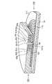
- FIG. 5is a perspective view of the gas supply unit as viewed from the lower surface side.
- FIG. 6is a diagram showing vortex flow in the gas flow space of the gas supply unit.
- 7A to 7Dare process diagrams of an ALD process performed using the film forming apparatus.
- FIGS. 8A to 8Care explanatory views showing a first modification of the gas supply unit.
- FIGS. 9A and 9Bare explanatory views showing a second modification of the gas supply unit.
- FIGS. 10A and 10Bare explanatory views showing a third modification of the gas supply unit.
- FIGS. 11A to 11Care explanatory views showing a second embodiment of the gas supply unit.
- FIG. 12is a longitudinal perspective view showing a third embodiment of the gas supply unit.
- FIGS. 13A and 13Bare a bottom view and a lower perspective view showing the lower side of the gas supply unit of the third embodiment.
- FIG. 14is a vertical perspective view showing the structure around the gas introduction port of the gas supply unit.
- FIGS. 15A and 15Bare views showing the gas concentration distribution in the processing space in the simulation of the evaluation test.
- FIG. 16is a perspective view of a gas channel model used in the simulation of the evaluation test.
- FIG. 17is a longitudinal sectional view of a conventional gas shower head.
- the film forming apparatus 2includes, for example, a source gas containing strontium (Sr) as a first process gas (hereinafter referred to as Sr source gas) and a source gas containing titanium (Ti) as a second process gas. (Hereinafter referred to as Ti source gas), these gases are reacted with ozone (O 3 ) gas, which is an oxidizing gas as a third processing gas, and a semiconductor wafer (hereinafter referred to as wafer) as a substrate by an ALD process. It has a function of forming a thin film of strontium titanate (SrTiO 3 , hereinafter abbreviated as STO), which is a high dielectric material, on the W surface.
- Sr source gasa source gas containing strontium (Sr) as a first process gas
- Tititanium
- ozone (O 3 ) gaswhich is an oxidizing gas as a third processing gas
- wafersemiconductor wafer
- the film forming apparatus 2includes a processing container 21.
- a mounting table 22 for mounting the wafer W horizontallyis provided in the processing container 21.
- a heater 22 a serving as a temperature control unit for the wafer Wis provided in the mounting table 22.
- the mounting table 22is provided with three lifting pins 22c (only two are shown for convenience) that can be lifted and lowered by a lifting mechanism 22b.
- the wafer Wis transferred between the wafer transfer mechanism (not shown) outside the film forming apparatus 2 and the mounting table 22 through the lift pins 22c.
- the one end side of the exhaust pipe 23is connected to the bottom of the processing vessel 21.
- An exhaust means 24composed of a vacuum pump or the like is connected to the other end side of the exhaust pipe 23.
- the exhaust means 24has a pressure adjusting mechanism (not shown), and can receive a control signal from the control unit 3A (described later) to maintain the pressure in the processing container 21 at a predetermined pressure during the film forming process. Yes.
- a transfer port 25 that is opened and closed by a gate valve Gis formed on the side wall of the processing vessel 21.
- Sis a processing space around the wafer W placed on the mounting table 22.
- the gas supply unit 3 constituting the gas supply device of the present inventionis provided above the processing container 21 so as to face the wafer W mounted on the mounting table 22.
- the gas supply unit 3will be described with reference to FIGS. 2 to 4 which are longitudinal side views thereof.
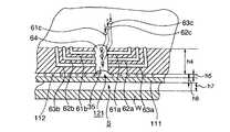
- the gas supply unit 3has a main body 31 formed in an inverted T shape when viewed from the side. That is, the main body portion 31 is formed in a cylindrical shape having a flat large diameter on the lower side and a cylindrical shape having a small diameter on the upper side.
- a gas flow space 32is formed in the main body 31 from the upper side to the lower side.
- the gas flow space 32has a generally conical shape that widens from the upper side toward the lower side.
- partition members 41 to 46are provided from the reduced diameter end 32a side to the enlarged diameter end 32b side of the gas flow space 32.
- Each of the partition members 41 to 46has a cylindrical shape whose diameter is increased from the reduced diameter end 32a side toward the enlarged diameter end 32b side.
- the partition members 41 to 46have different diameters, and are arranged in the order of the partition members 41, 42, 43, 44, 45, and 46 from the inner side to the outer side in the radial direction of the gas flow space 32.
- the partition members 41 to 46partition the gas flow space 32 concentrically to form gas flow paths 51 to 57.
- the extent of the expansion of one partition member(the magnitude of the angle with respect to the axial direction of the gas flow space 32) is larger than the extent of the expansion of the partition members adjacent to the inside in the radial direction. ing. That is, when the partition members 41 to 46 are arranged in descending order, the partition member 46> the partition member 45> the partition member 44> the partition member 43> the partition member 42> the partition member 41.
- FIG. 3is a cross-sectional view taken along the line AA in FIG. 2, and FIG. 5 is a perspective view of the main body 31 viewed from below.
- the partition members 41 to 46are supported by a plurality of support members 48 and 49 at their upper and lower ends, respectively.
- the support members 48 and 49extend in the radial direction in the gas flow space 32 from the inner peripheral surface 33 of the main body 31 toward the partition member 41 side. That is, the support members 48 and 49 spread radially from the inner partition member 41 toward the inner peripheral surface 33 of the main body 31.
- the support members 48 and 49have a role of supporting the partition members 41 to 46, and transmit heat from, for example, a temperature adjusting means such as the heater 34 provided in the main body 31, to the partition members 41 to 46.
- the processing gasis cooled on the surface of the partition members 41 to 46, and has a role of preventing film formation on the surface.
- the heater 34is provided in the main body 31 so as to surround the gas flow space 32 and the partition members 41 to 46, for example.
- the support members 48 and 49are not shown in FIG.
- a gas introduction path 35is formed on the upstream side of the gas flow space 32 in the main body 31 so as to extend in the axial direction of the gas flow space 32.
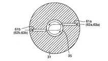
- gas introduction ports 61a, 61b, 62a, 62b, 63a, 63bfor supplying gas to the gas flow space 32 through the gas introduction path 35 are provided.
- the gas introduction ports 61a, 62a, 63aare formed in this order from the top to the bottom, and the gas introduction ports 61b, 62b, 63b are formed in this order from the top to the bottom.
- Each of the gas introduction ports 61a to 63a, 61b to 63bhas a circular vertical cross section as shown in FIG. 4, for example, and has a hole opened toward the side of the main body 31.
- the gas introduction ports 61a to 63a and the gas introduction ports 61b to 63bare It is arranged so as to be displaced.
- the gases supplied from the gas introduction ports 61a to 63a and 61b to 63btravel downward while forming a vortex that rotates in the circumferential direction in the gas introduction path 35 as shown in FIG.
- the height h1 of the gas introduction path 35 of the main body 31is, for example, 80 mm
- the height h2 from the reduced diameter end 32a of the gas flow space 32 to the upper ends of the partition members 41 to 46is, for example, 20 mm. It is.
- the height h3 from the upper end to the lower end of the partition members 41 to 46is, for example, 30 mm.
- the diameter R of the enlarged diameter end 32b of the gas flow space 32is, for example, 300 mm.
- gas supply lines 71 to 73 for supplying various gasesare connected to the gas introduction ports 61a to 63a and 61b to 63b. That is, the gas introduction ports 61a and 61b are connected to the Sr source gas supply line 71, the gas introduction ports 62a and 62b are connected to the Ti source gas supply line 72, and the gas introduction ports 63a and 63b are connected to the ozone gas supply line 73, respectively.
- the Sr source gas supply line 71is connected to an Sr source supply source 7A, and for example, Sr (THD) 2 (strontium bistetramethylheptanedionate) or Sr (Me 5 Cp) 2 (bis Liquid Sr raw materials such as pentamethylcyclopentadienyl strontium) are stored.
- Sr (THD) 2sinrontium bistetramethylheptanedionate
- Sr (Me 5 Cp) 2bis Liquid Sr raw materials such as pentamethylcyclopentadienyl strontium
- the Ti source gas supply line 72is connected to a Ti source supply source 7B, and for example, Ti (OiPr) 2 (THD) 2 (titanium bisisopropoxide bistetramethylheptanedionate) or Ti Ti raw material such as (OiPr) (titanium tetraisopropoxide) is stored, and Ti raw material gas vaporized by a vaporizer (not shown) is supplied as in the case of Sr raw material.
- TDDtitanium bisisopropoxide bistetramethylheptanedionate
- Ti Ti raw materialsuch as (OiPr) (titanium tetraisopropoxide
- the ozone gas supply line 73is connected to, for example, an ozone gas supply source 7C. Further, the Sr source gas supply line 71, the Ti source gas supply line 72, and the ozone gas supply line 73 are branched in the middle of the path and connected to the Ar (argon) gas supply source 7D, and together with the respective processing gases, Ar Gas can be supplied to the gas introduction ports 61a to 63a and 61b to 63b.
- the upstream end 35 a of the gas introduction path 35is opened at the upper part of the main body 31 to form a gas introduction port 64.
- One end of a gas supply line 74is connected to the gas introduction port 64.
- the other end of the gas supply line 74is connected to the Ar gas supply source 7D.
- This gas supply line 74promotes the gas flow in the gas flow space 32 by supplying Ar gas to the gas flow space 32, and in the film forming process described later, gas introduction ports 61a to 63a, 61b.
- the filmis efficiently formed by the processing gas supplied from .about.63b, and the purge process has a role of shortening the time required for the purge.
- the Ar gas from the gas supply line 74is called a counter gas.
- Each gas supply line 71-74is provided with a flow control device group 75, 76 consisting of valves, flow meters, etc., and supply timings and supply amounts of various gases based on instructions from the control unit 3A described later. Is controlled.
- the film forming apparatus 2is provided with a control unit 3A composed of, for example, a computer, and the control unit 3A includes a program.
- a command(each step) is incorporated so that a control signal is sent from the control unit 3A to each unit of the film forming apparatus 2 and the processing of the wafer W proceeds.
- This program(including programs related to processing parameter input operations and display) is stored in the storage unit 3B including a computer storage medium such as a flexible disk, a compact disk, a hard disk, and an MO (magneto-optical disk) and installed in the control unit 3A. Is done.
- the wafer Wis loaded into the processing container 21 through the transfer port 25 by an external wafer transfer mechanism.
- the wafer Wis mounted on the mounting table 22 via the lift pins 22c.
- the wafer Wis heated to a predetermined temperature and the processing chamber 21 is evacuated to a predetermined pressure.
- the STO film forming process by the ALD processis executed based on the gas supply sequence shown in FIGS. 7 (a) to 7 (d).
- the white columns shown in FIGS. 7A to 7Cshow the supply amount of the processing gas (Sr source gas, Ti source gas, ozone gas) from the gas supply lines 71 to 73, respectively. Yes. Also, the columns filled with hatched hatching in FIGS. 7A to 7D indicate the supply amounts of Ar gas from the gas supply lines 71 to 74, respectively.
- Sr source gas and Ar gasare supplied from the Sr source gas supply line 71 and Ar gas is supplied from the gas supply line 74 to the gas flow space 32 via the gas introduction path 35, respectively.
- Sr source gas supply stepin order to prevent Sr source gas from flowing into each gas introduction port and forming a film, Ti source gas supply line 72 and A small amount of Ar gas is also supplied from the ozone gas supply line 73 to the gas introduction path 35.
- Ar gasis supplied from a gas introduction port not used for film formation for the same reason.
- the Sr source gas and Ar gas supplied to these gas introduction paths 35form a vortex that rotates in the circumferential direction of the main body 31 as described above, and travel downstream through the gas introduction path 35 to enter the gas flow space 32. Inflow. These gases are dispersed in the gas flow paths 51 to 57 partitioned by the partition members 41 to 46 as shown by arrows in FIG. 2 and supplied to the surface of the wafer W, and the molecules constituting the Sr source gas are transferred to the wafer W. Adsorb to. Excess Sr source gas and Ar gas are exhausted through the exhaust pipe 23 and removed from the processing space S.
- the Ti source gas and the Ar gasare supplied from the Ti source gas supply line 72 as shown in FIGS. 7B and 7D.
- Ar gasis supplied from the supply line 74 to the gas introduction path 35 (Ti source gas supply process).
- Ti source gas and Ar gas supplied to these gas introduction paths 35are supplied to the wafer W through the gas flow space 32 in the same manner as the Sr source gas and Ar gas in the Sr source gas supply step described above.
- Molecules constituting the Ti source gasare adsorbed on the surface of the wafer W. Excess Ti source gas and Ar gas are removed from the processing vessel 21 through the exhaust pipe 23.
- Ti source gas purge stepWhen a predetermined time has elapsed and an adsorption layer of Ti source gas is formed on the wafer W, the supply of each gas is stopped, and as shown in FIGS. 7B and 7D, the Ti source gas supply line 72 and Ar gas is supplied as a purge gas from the counter gas supply line 74 to purge the Ti source gas remaining in the processing vessel 21 and the gas supply unit 3 (Ti source gas purge step).
- the ozone gas and the Ar gasare supplied from the ozone gas supply line 73 and the Ar gas is supplied from the gas supply line 74 to the Ar as shown in FIGS. 7 (c) and 7 (d).
- Each gasis supplied to the gas introduction path 35 (ozone gas supply process).
- the ozone gas and Ar gas supplied to the gas introduction path 35are supplied to the wafer W through the gas flow space 32 in the same manner as the Sr source gas and Ar gas in the Sr source gas supply process described above.
- the ozone gasreacts with the source gas molecules already adsorbed on the surface of the wafer W by the heat of the heater 22a of the mounting table 22 to form an STO molecular layer.
- the cycleis repeated a predetermined number of times, for example, 100 times, and the STO molecular layer is formed into multiple layers. Then, the formation of the STO film having a predetermined film thickness is completed. Then, after the film formation is completed, the supply of various gases is stopped, and the pressure in the processing vessel 21 is returned to the state before the vacuum exhaust, and then the wafer W is unloaded by an external transfer mechanism through a path opposite to that during loading, A series of film forming operations is completed.
- a gasis introduced, and the gas is supplied to the wafer W through the gas flow space 32 along the partition members 41 to 46 provided concentrically so that the extent of the spread becomes larger toward the outside. Therefore, the conductance (ease of gas flow) of the gas flow path until the wafer W is supplied can be increased. Therefore, in the ALD process as described above, the processing gas containing Sr source gas, Ti source gas or ozone gas can be supplied to the gas flow space 32 and then supplied to the wafer W at a high speed. Moreover, after supplying each source gas, the purge process which substitutes with Ar gas can be performed at high speed. For this reason, throughput can be improved.
- the gas supply unit 3does not have a structure that requires precise and complicated processing like the gas shower head described above, the gas supply unit 3 is easier to manufacture than the gas shower head.
- a material constituting the main body 31 and the partition members 41 to 46for example, aluminum, a mixture of SiC and aluminum, ceramics, or the like can be used.
- the degree of freedom of the material that can be used for manufacturing the gas supply unit 3is large.
- by selecting a material such as aluminum that is easy to work withit is possible to easily add or delete a gas introduction port according to the number of types of gas required for the process.
- a rod-shaped airflow control member 81is provided inside the partition member 41.
- the air flow control member 81is configured to prevent gas from flowing in the central region in the radial direction of the gas flow space 32.
- such an air flow control member 81is provided on the center side in the radial direction in which the gas is easily supplied, so that the gas is uniformly supplied to the entire wafer W and the in-plane processing is performed. Can improve the uniformity.
- FIG. 8Bis a perspective view of the airflow control member
- FIG. 8Cis a perspective view of the periphery of the airflow control member 81 on the lower surface side of the gas supply unit 3.
- the displayis omitted for convenience of illustration, but the support members 48 and 49 extend inside the partition member 41 and support the airflow control member 81.
- FIG. 9Ashows a second modification of the gas supply unit 3.
- a cylindrical partition member (airflow control member) 82whose upper end is closed is provided inside the partition member 41.
- the gasis prevented from flowing to the central region in the radial direction of the gas flow space 32, and the gas is uniformly supplied to the entire wafer W, thereby improving the in-plane processing uniformity.
- FIG. 9Bis a perspective view of the partition member 82.
- the partition member 82is supported by support members 48 and 49 extending radially inward of the gas flow space 32 in the same manner as the airflow control member 81, but the display is omitted in FIG. 9B for convenience of illustration. Yes.
- the uniformity of processing within the surface of the wafer Wis improved.
- the inclination and interval of the partition members 41 to 46 and the shapes of the airflow control member 81 and the partition member 82may be adjusted.
- the conductanceincreases in the gas flow paths 51 to 57 from the radially inner side to the outer side of the main body 31.
- the gas flow paths 51 to 57are arranged in descending order of conductance, the flow path 57> the flow path 56> the flow path 55> the flow path 54> the flow path 53> the flow path 52> the flow path 51. It is preferable. As a result, the gas is uniformly supplied in the plane of the wafer W, and a uniform film forming process can be performed in the plane of the wafer W.
- the conductances of the gas flow paths 51 to 57are made larger toward the outer side in the radial direction as described above.
- the supply of gasmay be made uniform.
- the number of partition members arranged in the gas flow space 32may be increased or decreased to make the gas supply uniform.
- a gas supply unit 9 as a third modification of the gas supply unitis shown in FIG.
- a partition member 91is provided in the gas introduction path 35 to partition the gas introduction path 35 into an inner region 92 and an outer region 93 in the radial direction.
- a partition member 94configured in the same manner as the partition member 41 is provided in the gas flow space 32.
- the lower end 91 a of the partition member 91is connected to the upstream end 94 a of the partition member 94.
- the gas introduction ports 61 a to 63 aare configured to supply each gas to the inner region 92, and a plurality of gases for diffusing the gas supplied to the inner region 92 to the outer region 93 are formed on the side wall of the partition member 91. An opening 95 is provided. Therefore, the gas from the gas introduction ports 61 a to 63 a is first supplied to the inner region 92 and then diffused from the inner region 92 to the outer region 93 through the plurality of openings 95. Even if the gas supply unit is configured in this manner, it is not necessary to pass gas through a complicated and fine flow path unlike a gas shower head, and thus the same effect as the example of the first embodiment can be obtained.
- the gas supply unit 100 shown in FIG. 11Ais configured in the same manner as the gas supply unit 3, but the partition members 41 to 46 described above are not provided in the gas flow space 32, and instead they are replaced.
- Plate-shaped partition members 103 to 106are provided so as to partition the gas flow space 32 in the circumferential direction. Each partition member 103 to 106 extends in the radial direction from the center of the gas flow space 32 toward the inner peripheral surface 33 of the main body 31.
- each partition member 103 to 106is supported by the inner peripheral surface 33 and the other end is supported by a support member 107 provided at the center in the radial direction.
- FIG. 11Cis a perspective view of the partition members 103 to 106 and the support member 107.
- FIG. 11Ashows the gas supplied from the gas introduction ports 61a to 63a and 61b to 63b, the gas supplied from the gas introduction ports is the same as in the first embodiment. While forming a swirl that rotates in the circumferential direction of the main body portion 31, the gas flow space 32 is directed toward the enlarged diameter end 32 b. The gas is guided by the partition members 103 to 106, and the vortex is discharged toward the wafer W from the enlarged diameter end 32b.
- FIG. 11Bshows the upper surface of the wafer W when the gas is supplied in this way, and the arrows indicate the gas flow.
- the partition members 103 to 106are configured so that the gas that forms a vortex as described above is supplied to the wafer W from the enlarged diameter end 32b of the gas flow space 32, and thus, the entire wafer W is highly uniform. It is preferable to supply gas.
- the partition members 103 to 106are preferably supported in an inclined state about the horizontal axis. In this case, the angles around the horizontal axis of the partition members 103 to 106 are set as appropriate.
- the partition members 103 to 106are provided at the enlarged diameter end 32b of the gas flow space 32, but may be formed to extend from the enlarged diameter end 32b to the reduced diameter end 32a. Further, the number of partition members is not limited to four so that gas can be uniformly supplied to the wafer W, and is set as appropriate.
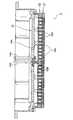
- FIG. 12is a cross-sectional perspective view of the present embodiment.
- the main body 120 of the gas supply unit 110 shown in FIG. 12has a flat circular shape.
- a disk-shaped gas flow space 121is formed in the main body 120 in place of the gas flow space 32 whose diameter is expanded on the lower side.
- the partition members 41 to 46are not provided in the gas flow space 121, and the plate-like member 111 is provided on the downstream end 121 a side of the gas flow space 121.
- a ring-shaped slit 112 divided into four in the circumferential directionis concentrically opened in the plate member 111.
- 13Ais a bottom view of the plate-shaped member 111
- FIG. 13Bis a perspective view of the plate-shaped member 111 as viewed from the lower side of the gas supply unit 110.
- 14 slits 112are opened from the center of the plate-like member 111 toward the periphery.
- the width of the two slits 112 formed on the most central sideis 2 mm
- the width of the seven slits 112 formed on the outside thereofis 3 mm
- the width of the three slits 112 formed on the outside thereofis 4 mm.
- the width of the two slits 112 formed on the outermost peripheral sideis 5 mm.
- the width of the slit 112is configured to increase as it goes toward the peripheral edge of the plate-like member 111, and the opening is not formed at the center of the plate-like member 111.
- the conductance of the gas on the peripheral side in the radial direction of the gas supply unit 110is increased as in the modification of the first embodiment, the gas is uniformly supplied to the entire wafer W, and the in-plane processing of the wafer W is performed. Can improve the uniformity.
- the length of the diameter L1 of the circle constituting the periphery of the slit 112 formed on the outermost side of the plate-like member 111is, for example, 300 mm.
- the distance L2 between the slits 112 adjacent in the circumferential directionis, for example, 7 mm.
- FIG. 14shows the structure of the gas introduction path 35 and its peripheral part, and in this example, Sr in four directions so that a vortex can be formed in the gas introduction path 35 as in the other embodiments.
- a gas introduction port for introducing gas, Ti gas, and O 3 gasis provided (the figure shows a cross-sectional shape, so the ports for introducing gas are shown in only three directions).
- the gas introduction ports 61c, 62c, and 63care formed as introduction paths for Sr gas, Ti gas, and O 3 gas, similarly to the gas introduction ports 61a, 62a, and 63a, respectively.
- Each gas introduction port(not shown) is provided so as to face these gas introduction ports 61c, 62c, 63c.
- the diameter of each gas introduction port for introducing these Sr gas, Ti gas and O 3 gasis, for example, 4 mm
- the diameter of the gas introduction port 64 for introducing Ar gasis, for example, 12 mm.
- the height h4 from the upper surface of the main body 120 to the upper surface of the gas flow space 121is, for example, 30 mm
- the height of the gas flow space 121 indicated by h5is, for example, 5 mm
- the thickness h6 of the plate member 111is, for example, 5 mm.
- the distance h7 between the wafer W surface and the lower surface of the plate-like member 111is, for example, 10 mm.
- the gas supply unit 110 of the third embodimentit is not necessary to pass gas through a complicated and fine flow path as compared with the conventional gas shower head shown in FIG. A decrease in conductance can be suppressed. Therefore, the same effect as the first embodiment can be obtained.
- the gas supply apparatus of the present inventionis applied to a film forming apparatus.
- a gasis supplied to a substrate, and the gas is supplied.
- the plasma etching apparatuswhich makes it plasma and etches a board
- the film forming apparatusis not limited to an apparatus that performs an ALD process in which different processing gases are intermittently supplied to a substrate in a predetermined cycle as described above, and the processing gas is continuously supplied to the wafer W and continuously.
- the semiconductor waferis described as an example of the substrate, but the present invention is not limited to this, and the present invention can be applied to a glass substrate, an LCD substrate, a ceramic substrate, and the like.
- the gas supply amount from the gas introduction ports 61a to 63a and 61b to 63bis 250 mL / min (sccm), and the supply amount from the gas introduction port 64 is 500 mL / min (sccm).
- the C 7 H 8 gas fraction and Ar gas fractionare 27% and 72%, respectively.
- the temperature of the wafer W and the processing space around itis set to 230 ° C., and gas is exhausted from the center of the wafer W to the radial direction at the outer periphery of the wafer W, so that the pressure in the processing space S becomes 45 Pa.
- FIG. 15Ashows the simulation result of the concentration distribution in the processing space S after 0.1 seconds after supplying the C 7 H 8 gas as described above.
- the gas concentration distribution in the processing space Sis shown in FIG. The area is indicated by isodensity lines. As shown in this figure, a substantially uniform distribution of C 7 H 8 gas is obtained.
- the actual simulation resultis output on a color screen so that the density distribution is displayed in gradation by computer graphics.
- FIG. 15A and FIG.The concentration distribution is shown. Accordingly, the concentration distribution is not actually skipped in FIGS. 15A and 15B, and there is a steep concentration gradient between the regions divided by the isoconcentration lines in these drawings. Means.
- FIG. 15Bshows the result of the simulation by dividing the gas concentration distribution by isoconcentration lines in the same manner as in FIG. 15A, and further, for convenience of illustration, a point indicating a predetermined concentration in the processing space S is shown.
- the C 7 H 8 gas concentration in the blackened regionis 19%, and the C 7 H 8 gas concentration in the region hatched with a solid line in one direction is 13%.
- C 7 H 8 gas concentration in the region indicated by hatching in netis 8%, C 7 H 8 gas concentration in the region marked with the point is 6%.
- the C 7 H 8 gas concentration in the hatched regionis smaller than 19% and larger than 13%.
- the C 7 H 8 gas concentration in the region without dots or linesis smaller than 13% and larger than 8%.
- the simulation result after 1.0 secondshowed a similar concentration difference. Also in the Sr source gas purge process, there was a location where the C 7 H 8 gas concentration was high in the shower head after 1.0 second had elapsed after gas supply.
- the gas supply unit 3 of the present inventioncan supply gas with high uniformity to the surface of the wafer W and can quickly perform the purge as compared with the conventional gas shower head.
- %indicates volume% concentration.
- evaluation test 2Similarly to the evaluation test 1, the ozone gas supply process in the gas supply unit 3 was simulated, and the concentration distribution in the ozone gas flow space 32 and the surface of the wafer W was examined. As a result, the concentration distribution in the flow space 32 and on the surface of the wafer W became substantially uniform 0.05 seconds after the gas was discharged. The speed until the concentration distribution becomes uniform is sufficient to perform the ALD process, and it is considered that the gas supply unit 3 is effective in the ALD process.
- the Ar gas flow rate from the gas introduction port 64was set to 500 mL / min (sccm), and a total of 500 mL / min (sccm) Ar gas was supplied from the gas introduction ports 62a and 62c. Other gas introduction ports are not set in this simulation. Then, the distribution of toluene gas in the processing space S was examined.
Landscapes
- Chemical & Material Sciences (AREA)
- Engineering & Computer Science (AREA)
- Chemical Kinetics & Catalysis (AREA)
- Materials Engineering (AREA)
- General Chemical & Material Sciences (AREA)
- Mechanical Engineering (AREA)
- Metallurgy (AREA)
- Organic Chemistry (AREA)
- Physics & Mathematics (AREA)
- Manufacturing & Machinery (AREA)
- Condensed Matter Physics & Semiconductors (AREA)
- General Physics & Mathematics (AREA)
- Computer Hardware Design (AREA)
- Microelectronics & Electronic Packaging (AREA)
- Power Engineering (AREA)
- Inorganic Chemistry (AREA)
- Plasma & Fusion (AREA)
- Chemical Vapour Deposition (AREA)
Abstract
Description
本発明は、基板に対して処理ガスを供給するためのガス供給装置、当該ガス供給装置を備えた処理装置、ガス供給装置を用いた処理方法、及び記憶媒体に関する。The present invention relates to a gas supply apparatus for supplying a processing gas to a substrate, a processing apparatus including the gas supply apparatus, a processing method using the gas supply apparatus, and a storage medium.
CVD(chemical vapor deposition)およびエッチングなどを行う装置へのガス供給装置として、ガスシャワーヘッドが用いられている。このガスシャワーヘッドは、扁平な円柱形状に形成され、上部に設けられたガス導入ポートから供給されたガスを内部の拡散空間にて拡散させて、下面に形成された多数の孔からシャワー状に供給する。複数種類の処理ガスを供給するガスシャワーヘッドとしては、一系統のガス流路の途中で複数種類の処理ガスを混合してから供給するいわゆるプリミックス方式のものと、複数種類のガスに対して個別にガス流路を設けて供給するポストミックス方式のものとがある。A gas shower head is used as a gas supply device to a device that performs CVD (chemical vapor deposition) and etching. This gas shower head is formed in a flat cylindrical shape, diffuses the gas supplied from the gas introduction port provided in the upper part in the internal diffusion space, and forms a shower from a number of holes formed in the lower surface. Supply. As a gas shower head that supplies a plurality of types of processing gas, a so-called premix system that supplies a mixture of a plurality of types of processing gas in the middle of a single gas flow path, and a plurality of types of gases. There is a post-mix type that supplies gas flow paths separately.
一方、成膜方法として複数種類の処理ガスの供給を例えば2ステップに分けて、第1の処理ガスの供給を行う第1のステップと、第2の処理ガスの供給を行う第2のステップと、を交互に行うことによりこれら処理ガスによる反応生成物を順次積層して、成膜を行ういわゆるALD(Atomic Layer Deposition)も知られている。On the other hand, as a film forming method, the supply of a plurality of types of processing gases is divided into two steps, for example, a first step for supplying a first processing gas, and a second step for supplying a second processing gas. A so-called ALD (Atomic Layer Deposition) is also known in which the reaction products of these processing gases are sequentially stacked to form a film.
シャワーヘッド内のガス流路は複雑で狭いことからコンダクタンスが低く、ガスの置換性が悪い。このためALDの場合には、時間的に前後して供給される複数の処理ガスがシャワーヘッド内部で混じりあって反応生成物が生じるのを避けるために上記のポストミックスタイプのシャワーヘッドが用いられる。The gas flow path in the shower head is complicated and narrow, so the conductance is low and the gas replacement property is poor. For this reason, in the case of ALD, the above-described post-mix type shower head is used in order to avoid a reaction product from being generated by mixing a plurality of processing gases supplied before and after in the shower head. .
図17は前記ガスシャワーヘッドの一例の縦断側面を示したものである。このガスシャワーヘッド1は夫々扁平な円形のシャワープレート11、本体部12、ベース部材13などの複数の部材が接合された積層構造となっている。第1のガス供給管14Aから供給された第1のガスは、本体部12とベース部材13との間に形成されたガス拡散空間15Aに拡散して第1の吐出口16Aに供給される。第2のガス供給管14Bから供給された第2のガスは、本体部材12とシャワープレート11との間に形成されたガス拡散空間15Bに拡散して第2の吐出口16Bに供給される。このように、第1のガス及び第2のガスはガスシャワーヘッド1内で混ざり合わないように独立して吐出口16A,16Bから夫々吐出される。FIG. 17 shows a longitudinal side surface of an example of the gas shower head. Thegas shower head 1 has a laminated structure in which a plurality of members such as a flatcircular shower plate 11, amain body 12, and abase member 13 are joined. The first gas supplied from the firstgas supply pipe 14A diffuses into thegas diffusion space 15A formed between themain body 12 and thebase member 13, and is supplied to thefirst discharge port 16A. The second gas supplied from the secondgas supply pipe 14B diffuses into thegas diffusion space 15B formed between themain body member 12 and theshower plate 11, and is supplied to thesecond discharge port 16B. As described above, the first gas and the second gas are independently discharged from thedischarge ports gas shower head 1.
ところでALDのプロセスにおいて、ガスシャワーヘッド1から供給される処理ガスの種類を切り替える際には、次の処理ガスの供給を開始する前にパージガスを供給し、成膜を行う処理雰囲気内に残っている処理ガスを完全に排除(パージ)する工程が必要である。スループットを向上させるため、この処理ガスの切り替え間におけるパージガスを供給する工程はできるだけ短い時間であることが好ましい。In the ALD process, when the type of processing gas supplied from thegas showerhead 1 is switched, a purge gas is supplied before starting the next processing gas supply, and remains in the processing atmosphere in which film formation is performed. It is necessary to completely remove (purge) the processing gas. In order to improve the throughput, it is preferable that the process of supplying the purge gas between the process gas switching is as short as possible.
しかしながら、このガスシャワーヘッド1においては、既述のように流路におけるガスのコンダクタンスが低いことから、パージガスを供給する時間が短いと、ガス拡散空間15A,15Bの隅部などにおいて処理ガスが残留してしまうおそれがある。However, in thegas shower head 1, since the gas conductance in the flow path is low as described above, if the purge gas supply time is short, the processing gas remains in the corners of thegas diffusion spaces
このように先に供給された処理ガスがシャワーヘッド内に残留した状態で次の処理ガスが供給されると、この残留ガスがウエハの処理空間に流出してしまう。この結果、先に供給された処理ガスと、次に供給された処理ガスとがガスシャワーヘッド1の表面で反応して堆積物が付着する。この結果、パーティクル汚染の要因となったり、ウエハ上に反応生成物がパーティクルとして直接付着し、ウエハWの成膜処理が正常に行われないおそれがある。従ってパージの時間をあまり短くすることができず、スループットの向上が困難な状況にある。If the next processing gas is supplied in a state where the previously supplied processing gas remains in the shower head, the residual gas flows out into the processing space of the wafer. As a result, the processing gas supplied first and the processing gas supplied next react on the surface of thegas shower head 1 to deposit. As a result, there is a risk of particle contamination, or reaction products may directly adhere to the wafer as particles, and the film formation process of the wafer W may not be performed normally. Therefore, the purge time cannot be shortened so much and it is difficult to improve the throughput.
また、上述のALD、CVD、プラズマエッチング処理などにおいてはウエハを所定の温度に加熱するため、ウエハWの周囲の処理空間は加熱される。従ってガスシャワーヘッド1を構成する材質として、熱膨張率が小さいSiCとアルミニウムとを混合したものまたはセラミックスなどの材質を用いて構成することが好ましい場合がある。しかしながら、上記のようにガスシャワーヘッドは複雑な積層構造を有し、微細な流路を形成する必要がある。特にシャワープレート11には多数の穴を穿孔する必要があり、上述の各材質にこのような微細な加工を施すことは難しい。このためシャワープレート11の製造が困難であったり、製造に使用できる材質が限られるという問題もあった。Further, in the above-described ALD, CVD, plasma etching processing, etc., the processing space around the wafer W is heated in order to heat the wafer to a predetermined temperature. Therefore, as a material constituting thegas shower head 1, it may be preferable to use a material such as a mixture of SiC and aluminum having a low coefficient of thermal expansion or ceramics. However, as described above, the gas shower head has a complicated laminated structure and needs to form fine flow paths. In particular, it is necessary to drill a large number of holes in theshower plate 11, and it is difficult to perform such fine processing on the above-described materials. For this reason, there is a problem that theshower plate 11 is difficult to manufacture or the materials that can be used for manufacturing are limited.
なお、特開平7-22323には、各種のガスを下方に広がる流路から夫々供給する気相成長装置について記載されている。しかしながら、特開平7-22323には、ガスを互いに置換する際に生じる上述した問題の解決方法については記載されていない。
特開平7-22323
JP-A-7-22323
本発明はこのような点を考慮してなされたものであり、基板に対してガスを供給してガス処理を行うにあたり、その内部の流路におけるガスの置換を高速で行うことができるガス供給装置、そのガス供給装置を備えた処理装置、そのガス供給装置を用いた処理方法、及び記憶媒体を提供することを目的とする。The present invention has been made in consideration of such points, and in supplying a gas to a substrate to perform gas processing, a gas supply capable of performing high-speed gas replacement in the flow path inside the substrate. It is an object of the present invention to provide an apparatus, a processing apparatus including the gas supply device, a processing method using the gas supply device, and a storage medium.
本発明は、処理容器内の基板に対向して配置され、前記基板にガスを供給してガス処理を行うためのガス供給装置において、縮径端と拡径端とを有するとともに概ね円錐形状からなり、前記縮径端側から前記拡径端側に前記ガスが通流されるガス通流空間を有する本体部と、前記本体部のうち前記ガス通流空間の前記縮径端側に設けられ、前記ガス通流空間に前記ガスを導入するためのガス導入ポートと、前記本体部の前記ガス通流空間内に設けられ、前記ガス通流空間を同心円状に区画する複数の区画部材と、を備え、一の区画部材の末広がりの程度は、径方向内側に隣接する区画部材の末広がりの程度より大きくなることを特徴とするガス供給装置である。The present invention provides a gas supply device that is disposed to face a substrate in a processing container and supplies gas to the substrate to perform gas processing, and has a reduced diameter end and an enlarged diameter end, and has a substantially conical shape. A main body portion having a gas flow space through which the gas flows from the reduced diameter end side to the enlarged diameter end side, and provided on the reduced diameter end side of the gas flow space of the main body portion, A gas introduction port for introducing the gas into the gas flow space, and a plurality of partition members provided in the gas flow space of the main body portion and partitioning the gas flow space concentrically. The gas supply device is characterized in that the degree of the spread of one partition member is larger than the extent of the spread of a partition member adjacent to the inside in the radial direction.
本発明は、前記本体部のうち前記ガス通流空間の上流側に、前記ガス通流空間の軸方向に伸びるガス導入路が形成され、前記ガス導入ポートは、前記ガス導入路の上流側に設けられていることを特徴とするガス供給装置である。In the present invention, a gas introduction path extending in the axial direction of the gas flow space is formed on the upstream side of the gas flow space in the main body, and the gas introduction port is located on the upstream side of the gas flow path. A gas supply device is provided.
本発明は、前記区画部材は、前記本体部の内周面から径方向内方に延びる支持部材によって支持されていることを特徴とするガス供給装置である。The present invention is the gas supply device, wherein the partition member is supported by a support member extending radially inward from the inner peripheral surface of the main body.
本発明は、前記区画部材により前記ガス通流空間が複数の流路に区画され、各前記流路は、径方向内側の流路のコンダクタンスが径方向外側の流路のコンダクタンスよりも小さくなるように設定されていることを特徴とするガス供給装置である。In the present invention, the gas flow space is partitioned into a plurality of flow paths by the partition member, and each of the flow paths has a conductance of a radially inner flow path smaller than a conductance of a radially outer flow path. The gas supply device is characterized in that it is set to.
本発明は、前記ガス通流空間の径方向の中心領域に、前記中心領域にガスが流れないようにするための気流制御部材が設けられていることを特徴とするガス供給装置である。The present invention is a gas supply device characterized in that an airflow control member for preventing gas from flowing into the central region is provided in a central region in the radial direction of the gas flow space.
本発明は、前記ガス導入路内に、前記ガス導入路を径方向に内側領域と外側領域とに仕切ると共に、前記内側領域に供給されたガスを前記外側領域に拡散させるための複数の開口部が形成された仕切り部材が設けられ、前記ガス導入ポートからのガスは、前記内側領域に供給されることを特徴とするガス供給装置である。In the gas introduction path, the present invention divides the gas introduction path into an inner area and an outer area in the radial direction, and a plurality of openings for diffusing the gas supplied to the inner area to the outer area. The gas supply device is characterized in that a partition member is formed, and gas from the gas introduction port is supplied to the inner region.
本発明は、前記仕切り部材は、前記区画部材の上流端に連接されていることを特徴とするガス供給装置である。The present invention is the gas supply device, wherein the partition member is connected to the upstream end of the partition member.
本発明は、処理容器内の基板に対向して配置され、前記基板にガスを供給してガス処理を行うためのガス供給装置において、縮径端と拡径端とを有するとともに概ね円錐形状からなり、前記縮径端側から前記拡径端側に前記ガスが通流されるガス通流空間を有する本体部と、前記本体部のうち前記ガス通流空間の前記縮径端側に設けられ、前記ガス通流空間に前記ガスを導入するためのガス導入ポートと、前記本体部の前記ガス通流空間内に設けられ、前記ガス通流空間を、周方向に区画するための複数の区画部材と、を備えたことを特徴とするガス供給装置である。The present invention provides a gas supply device that is disposed to face a substrate in a processing container and supplies gas to the substrate to perform gas processing, and has a reduced diameter end and an enlarged diameter end, and has a substantially conical shape. A main body portion having a gas flow space through which the gas flows from the reduced diameter end side to the enlarged diameter end side, and provided on the reduced diameter end side of the gas flow space of the main body portion, A gas introduction port for introducing the gas into the gas flow space, and a plurality of partition members provided in the gas flow space of the main body portion and for partitioning the gas flow space in the circumferential direction And a gas supply device.
本発明は、前記本体部のうち前記ガス通流空間の上流側に、前記ガス通流空間の軸方向に伸びるガス導入路が形成され、前記ガス導入ポートは、前記ガス導入路の上流側に設けられていることを特徴とするガス供給装置である。In the present invention, a gas introduction path extending in the axial direction of the gas flow space is formed on the upstream side of the gas flow space in the main body, and the gas introduction port is located on the upstream side of the gas flow path. A gas supply device is provided.
本発明は、前記複数の区画部材は、前記ガス通流空間の前記拡径端からの前記ガスが前記本体部の周方向に回転する渦流を形成しながら吐出するように構成されていることを特徴とするガス供給装置である。In the present invention, the plurality of partition members are configured to discharge the gas from the enlarged diameter end of the gas flow space while forming a swirl that rotates in a circumferential direction of the main body. This is a gas supply device.
本発明は、前記区画部材は、前記ガス通流空間の中心から径方向に延びることを特徴とするガス供給装置である。The present invention is the gas supply device, wherein the partition member extends in a radial direction from a center of the gas flow space.
本発明は、前記区画部材は、前記ガス通流空間において前記縮径端から前記拡径端に亘って設けられていることを特徴とするガス供給装置である。The present invention is the gas supply device, wherein the partition member is provided from the reduced diameter end to the enlarged diameter end in the gas flow space.
本発明は、処理容器内の基板に対向して配置され、前記基板にガスを供給してガス処理を行うためのガス供給装置において、前記ガスを通流させるためのガス通流空間を有する本体部と、前記本体部のうち前記ガス通流空間の上流端側に設けられ、前記ガス通流空間に前記ガスを導入するためのガス導入ポートと、前記本体部の前記ガス通流空間の下流端側に設けられ、前記ガス通流空間に供給された前記ガスを前記基板に供給するための同心円状に開口した複数のスリットを有する板状部材と、を備えたことを特徴とするガス供給装置である。The present invention is a gas supply device that is disposed to face a substrate in a processing container and supplies gas to the substrate to perform gas processing, and a main body having a gas flow space for allowing the gas to flow therethrough A gas inlet port for introducing the gas into the gas flow space, and a downstream of the gas flow space of the main body portion. A gas supply comprising: a plate-like member provided on an end side and having a plurality of concentrically opened slits for supplying the gas supplied to the gas flow space to the substrate. Device.
本発明は、前記本体部のうち前記ガス通流空間の上流側に、前記ガス通流空間の軸方向に伸びるガス導入路が形成され、前記ガス導入ポートは、前記ガス導入路の上流側に設けられていることを特徴とするガス供給装置である。In the present invention, a gas introduction path extending in the axial direction of the gas flow space is formed on the upstream side of the gas flow space in the main body, and the gas introduction port is located on the upstream side of the gas flow path. A gas supply device is provided.
本発明は、前記スリットは、前記板状部材の中心部から周縁部に向かうにつれてその開口幅が大きくなるように形成されていることを特徴とするガス供給装置である。The present invention is the gas supply device, wherein the slit is formed such that an opening width thereof increases from a center portion of the plate-shaped member toward a peripheral portion.
本発明は、前記本体部に温調手段が設けられていることを特徴とするガス供給装置である。The present invention is a gas supply device characterized in that a temperature control means is provided in the main body.
本発明は、基板を載置するための載置台と、前記載置台が内部に設けられた処理容器と、前記載置台に対向して設けられ、前記処理容器内に前記基板を処理するための処理ガスを供給するガス供給装置と、前記処理容器内を排気する排気手段と、を備え、前記ガス供給装置は、縮径端と拡径端とを有するとともに概ね円錐形状からなり、前記縮径端側から前記拡径端側に前記ガスが通流されるガス通流空間を有する本体部と、前記本体部のうち前記ガス通流空間の前記縮径端側に設けられ、前記ガス通流空間に前記ガスを導入するためのガス導入ポートと、前記本体部の前記ガス通流空間内に設けられ、前記ガス通流空間を同心円状に区画する複数の区画部材と、を有し、一の区画部材の末広がりの程度は、径方向内側に隣接する区画部材の末広がりの程度より大きくなることを特徴とする処理装置である。The present invention provides a mounting table for mounting a substrate, a processing container in which the mounting table is provided, a counter for the mounting table, and processing the substrate in the processing container. A gas supply device for supplying a processing gas; and an exhaust means for exhausting the inside of the processing container. The gas supply device has a reduced diameter end and an enlarged diameter end, and has a substantially conical shape. A main body having a gas flow space through which the gas flows from the end side to the enlarged diameter end side; and the gas flow space provided on the reduced diameter end side of the gas flow space in the main body portion. A gas introduction port for introducing the gas into the gas flow space, and a plurality of partition members that are provided in the gas flow space of the main body and divide the gas flow space concentrically, The extent of the end of the partition member is the partition member adjacent to the inside in the radial direction. A processing apparatus characterized by greater than the degree diverging.
本発明は、前記ガス供給装置の前記ガス導入ポートに接続され、複数種類の処理ガスを夫々供給するための複数の処理ガス用流路と、前記ガス供給装置の前記ガス導入ポートに接続され、パージ用の不活性ガスを供給するパージ用ガス流路と、前記複数の処理ガス用流路および前記パージ用ガス流路におけるガスの供給を制御するガス供給機器と、前記複数種類の処理ガスを順番にかつサイクリックに供給すると共に一の処理ガスの供給ステップと他の処理ガスの供給ステップとの間には、前記不活性ガスの供給ステップを行うように前記ガス供給機器を制御する制御部と、を更に備え、前記基板の表面に前記複数種類の処理ガスの反応生成物からなる層が順次積層されて薄膜が成膜されることを特徴とする処理装置である。The present invention is connected to the gas introduction port of the gas supply device, and is connected to a plurality of processing gas flow paths for supplying a plurality of types of processing gases, and to the gas introduction port of the gas supply device, A purge gas flow path for supplying an inert gas for purge; a gas supply device for controlling gas supply in the plurality of process gas flow paths and the purge gas flow path; and the plurality of types of process gases. A controller that sequentially and cyclically supplies and controls the gas supply device to perform the inert gas supply step between the supply step of one process gas and the supply step of another process gas. And a layer formed of reaction products of the plurality of types of processing gases is sequentially stacked on the surface of the substrate to form a thin film.
本発明は、処理容器の内部の載置台に基板を載置する工程と、前記載置台に対向して設けられたガス供給装置から、前記処理容器内に前記基板を処理するためのガスを供給する工程と、前記処理容器内を排気する工程と、を備え、前記ガス供給装置は、縮径端と拡径端とを有するとともに概ね円錐形状からなり、前記縮径端側から前記拡径端側に前記ガスが通流されるガス通流空間を有する本体部と、前記本体部のうち前記ガス通流空間の前記縮径端側に設けられ、前記ガス通流空間に前記ガスを導入するためのガス導入ポートと、前記本体部の前記ガス通流空間内に設けられ、前記ガス通流空間を同心円状に区画する複数の区画部材と、を有し、一の区画部材の末広がりの程度は、径方向内側に隣接する区画部材の末広がりの程度より大きくなることを特徴とする処理方法である。The present invention supplies a gas for processing the substrate into the processing container from a step of mounting the substrate on a mounting table inside the processing container and a gas supply device provided facing the mounting table. And a step of evacuating the inside of the processing container, wherein the gas supply device has a reduced diameter end and an enlarged diameter end, and has a substantially conical shape, and the enlarged diameter end from the reduced diameter end side. A main body portion having a gas flow space through which the gas flows, and a gas flow space provided on the reduced diameter end side of the gas flow space in the main body portion to introduce the gas into the gas flow space A gas introduction port, and a plurality of partition members provided in the gas flow space of the main body portion and concentrically dividing the gas flow space, and the extent of the end of one partition member is , Larger than the extent of expansion of the partition member adjacent to the inside in the radial direction It is a process wherein the Kunar.
本発明は、前記処理ガスを供給する工程は、複数種類の処理ガスを順番にかつサイクリックに供給すると共に一の処理ガスの供給ステップと他の処理ガスの供給ステップとの間には、不活性ガスの供給ステップを行う工程を有し、前記基板の表面に前記複数種類の処理ガスの反応生成物からなる層が順次積層されて薄膜が成膜されることを特徴とする処理方法である。According to the present invention, the process gas supply step includes supplying a plurality of types of process gases in order and cyclically, and between a process gas supply step and another process gas supply step. And a step of supplying an active gas, wherein a thin film is formed by sequentially laminating layers of reaction products of the plurality of types of processing gases on the surface of the substrate. .
本発明は、処理方法に用いられ、コンピュータ上で動作するコンピュータプログラムを格納した記憶媒体であって、前記処理方法は、処理容器の内部の載置台に基板を載置する工程と、前記載置台に対向して設けられたガス供給装置から、前記処理容器内に基板を処理するためのガスを供給する工程と、前記処理容器内を排気する工程と、を備え、前記ガス供給装置は、縮径端と拡径端とを有するとともに概ね円錐形状からなり、前記縮径端側から前記拡径端側に前記ガスが通流されるガス通流空間を有する本体部と、前記本体部のうち前記ガス通流空間の前記縮径端側に設けられ、前記ガス通流空間に前記ガスを導入するためのガス導入ポートと、前記本体部の前記ガス通流空間内に設けられ、前記ガス通流空間を同心円状に区画する複数の区画部材と、を有し、一の区画部材の末広がりの程度は、径方向内側に隣接する区画部材の末広がりの程度より大きくなることを特徴とする記憶媒体である。The present invention is a storage medium for storing a computer program used on a processing method and operating on a computer, the processing method comprising a step of mounting a substrate on a mounting table inside a processing container, and the mounting table described above A process for supplying a gas for processing the substrate into the processing container, and a process for exhausting the processing container. A main body having a gas flow space through which the gas flows from the diameter-reduced end side to the diameter-expanded end side, and having a diameter end and an enlarged diameter end; A gas introduction port provided on the reduced diameter end side of the gas flow space, for introducing the gas into the gas flow space, and provided in the gas flow space of the main body; A compound that divides the space into concentric circles. Has a partition member, a degree divergent one partition member is a storage medium characterized by greater than the degree diverging partition member adjacent radially inwardly.
本発明によれば、基板に供給するまでのガスの流路のコンダクタンスを大きくすることができ、ガス通流空間におけるガスの置換を速やかに行うことができる。また、本発明のガス供給装置は従来のように各段の部材に精密に複雑な加工を要する構造ではないので、製造が容易である。また、そのため使用できる材質の選択の自由度が大きい利点もある。また、このガス供給装置を用いていわゆるALDなどと呼ばれている複数の処理ガスを順番にサイクリックに供給して成膜を行う方式を用いた場合にパージガスによるガス供給装置内のガスの置換を高速に行うことができることから、スループットの向上に寄与することができる。According to the present invention, it is possible to increase the conductance of the gas flow path until the gas is supplied to the substrate, and it is possible to quickly replace the gas in the gas flow space. Further, the gas supply device of the present invention is easy to manufacture because it is not a structure that requires precise and complicated processing for each stage member as in the prior art. For this reason, there is also an advantage that the degree of freedom of selection of usable materials is great. In addition, when a film forming method is used in which a plurality of processing gases called so-called ALD are cyclically supplied to form a film using this gas supply device, the gas in the gas supply device is replaced with a purge gas. Can be performed at high speed, which can contribute to an improvement in throughput.
(第1の実施形態)
先ず、本発明の実施の形態である成膜装置2の全体構成について図1を参照しながら説明する。(First embodiment)
First, an overall configuration of afilm forming apparatus 2 according to an embodiment of the present invention will be described with reference to FIG.
先ず、本発明の実施の形態である成膜装置2の全体構成について図1を参照しながら説明する。(First embodiment)
First, an overall configuration of a
本実施の形態に係る成膜装置2は、例えば第1の処理ガスとしてストロンチウム(Sr)を含む原料ガス(以下、Sr原料ガスという)、第2の処理ガスとしてチタン(Ti)を含む原料ガス(以下、Ti原料ガスという)を用い、これらのガスを第3の処理ガスとしての酸化ガスであるオゾン(O3)ガスと反応させて、ALDプロセスにより、基板である半導体ウエハ(以下、ウエハと記載する)W表面に高誘電体材料であるチタン酸ストロンチウム(SrTiO3、以下STOと略記する)の薄膜を成膜する機能を備えている。Thefilm forming apparatus 2 according to the present embodiment includes, for example, a source gas containing strontium (Sr) as a first process gas (hereinafter referred to as Sr source gas) and a source gas containing titanium (Ti) as a second process gas. (Hereinafter referred to as Ti source gas), these gases are reacted with ozone (O3 ) gas, which is an oxidizing gas as a third processing gas, and a semiconductor wafer (hereinafter referred to as wafer) as a substrate by an ALD process. It has a function of forming a thin film of strontium titanate (SrTiO3 , hereinafter abbreviated as STO), which is a high dielectric material, on the W surface.
成膜装置2は、処理容器21を備えている。処理容器21内には、ウエハWを水平に載置するための載置台22が設けられている。載置台22内には、ウエハWの温調手段をなすヒータ22aが設けられている。更に載置台22には、昇降機構22bにより昇降自在な3本の昇降ピン22c(便宜上2本のみ図示)が設けられている。この昇降ピン22cを介して成膜装置2の外部の不図示のウエハ搬送機構と載置台22との間でウエハWの受け渡しが行われる。Thefilm forming apparatus 2 includes aprocessing container 21. A mounting table 22 for mounting the wafer W horizontally is provided in theprocessing container 21. In the mounting table 22, aheater 22 a serving as a temperature control unit for the wafer W is provided. Further, the mounting table 22 is provided with three liftingpins 22c (only two are shown for convenience) that can be lifted and lowered by alifting mechanism 22b. The wafer W is transferred between the wafer transfer mechanism (not shown) outside thefilm forming apparatus 2 and the mounting table 22 through the lift pins 22c.
処理容器21の底部には排気管23の一端側が接続されている。この排気管23の他端側には真空ポンプなどにより構成される排気手段24が接続されている。排気手段24は図示しない圧力調整機構を有し、これにより後述の制御部3Aからの制御信号を受けて、成膜処理中に処理容器21内の圧力を所定の圧力に維持できるようになっている。また処理容器21の側壁には、ゲートバルブGにより開閉される搬送口25が形成されている。図中Sは載置台22に載置されたウエハWの周囲の処理空間である。The one end side of theexhaust pipe 23 is connected to the bottom of theprocessing vessel 21. An exhaust means 24 composed of a vacuum pump or the like is connected to the other end side of theexhaust pipe 23. The exhaust means 24 has a pressure adjusting mechanism (not shown), and can receive a control signal from thecontrol unit 3A (described later) to maintain the pressure in theprocessing container 21 at a predetermined pressure during the film forming process. Yes. Atransfer port 25 that is opened and closed by a gate valve G is formed on the side wall of theprocessing vessel 21. In the figure, S is a processing space around the wafer W placed on the mounting table 22.
処理容器21の上部には、載置台22に載置されるウエハWに対向するように本発明のガス供給装置を構成するガス供給部3が設けられている。このガス供給部3について、その縦断側面図である図2乃至図4を参照しながら説明する。Thegas supply unit 3 constituting the gas supply device of the present invention is provided above theprocessing container 21 so as to face the wafer W mounted on the mounting table 22. Thegas supply unit 3 will be described with reference to FIGS. 2 to 4 which are longitudinal side views thereof.
ガス供給部3は、側面視逆T字状に形成された本体部31を有している。すなわち本体部31は、その下部側が扁平な大径の円柱形状に形成され、その上部側が小径の円柱形状に形成されている。本体部31の内部には、上方側から下方側へ向かうガス通流空間32が形成されている。ガス通流空間32は、上方側から下方側へ向かって広がる概ね円錐形状に構成されている。Thegas supply unit 3 has amain body 31 formed in an inverted T shape when viewed from the side. That is, themain body portion 31 is formed in a cylindrical shape having a flat large diameter on the lower side and a cylindrical shape having a small diameter on the upper side. Agas flow space 32 is formed in themain body 31 from the upper side to the lower side. Thegas flow space 32 has a generally conical shape that widens from the upper side toward the lower side.
本体部31のガス通流空間32内において、区画部材41~46が当該ガス通流空間32の縮径端32a側から拡径端32b側に亘って設けられている。各区画部材41~46は、前記縮径端32a側から拡径端32b側に向かうに従って拡径された筒状に構成されている。区画部材41~46は互いに異なる径を有し、区画部材41、42、43、44、45、46の順にガス通流空間32の径方向に内側から外側へ向けて配置されている。また区画部材41~46は、当該ガス通流空間32を同心円状に区画して、ガス流路51~57を形成している。ここで、区画部材41~46のうち一の区画部材の末広がりの程度(ガス通流空間32の軸方向に対する角度の大きさ)は、径方向内側に隣接する区画部材の末広がりの程度より大きくなっている。すなわち、区画部材41~46を末広がりの程度が大きいものから順に並べた場合、区画部材46>区画部材45>区画部材44>区画部材43>区画部材42>区画部材41となっている。In thegas flow space 32 of themain body 31,partition members 41 to 46 are provided from the reduceddiameter end 32a side to theenlarged diameter end 32b side of thegas flow space 32. Each of thepartition members 41 to 46 has a cylindrical shape whose diameter is increased from the reduceddiameter end 32a side toward theenlarged diameter end 32b side. Thepartition members 41 to 46 have different diameters, and are arranged in the order of thepartition members gas flow space 32. Thepartition members 41 to 46 partition thegas flow space 32 concentrically to formgas flow paths 51 to 57. Here, of thepartition members 41 to 46, the extent of the expansion of one partition member (the magnitude of the angle with respect to the axial direction of the gas flow space 32) is larger than the extent of the expansion of the partition members adjacent to the inside in the radial direction. ing. That is, when thepartition members 41 to 46 are arranged in descending order, thepartition member 46> thepartition member 45> thepartition member 44> thepartition member 43> thepartition member 42> thepartition member 41.
図3は、図2のA-A矢視断面図、図5は本体部31を下方側から見た斜視図である。これらの図に示すように、区画部材41~46は、その上端、下端において夫々複数の支持部材48、49により支持されている。支持部材48、49は、夫々本体部31の内周面33から区画部材41側に向かって、ガス通流空間32を径方向に伸びている。すなわち支持部材48、49は、夫々内側の区画部材41から本体部31の内周面33へ向けて放射状に広がっている。この支持部材48、49は、区画部材41~46を支持する役割を有する他に、例えば本体部31に設けられた温調手段例えばヒータ34などの熱を区画部材41~46へと伝達し、処理ガスが区画部材41~46表面で冷却されて当該表面に成膜が生じることを防ぐ役割を有する。FIG. 3 is a cross-sectional view taken along the line AA in FIG. 2, and FIG. 5 is a perspective view of themain body 31 viewed from below. As shown in these drawings, thepartition members 41 to 46 are supported by a plurality ofsupport members support members gas flow space 32 from the innerperipheral surface 33 of themain body 31 toward thepartition member 41 side. That is, thesupport members inner partition member 41 toward the innerperipheral surface 33 of themain body 31. Thesupport members partition members 41 to 46, and transmit heat from, for example, a temperature adjusting means such as theheater 34 provided in themain body 31, to thepartition members 41 to 46. The processing gas is cooled on the surface of thepartition members 41 to 46, and has a role of preventing film formation on the surface.
また図3に示すように、ヒータ34は、例えばガス通流空間32及び区画部材41~46を囲むように本体部31に設けられている。なお、図示の便宜上図4では支持部材48、49の表示を省略している。Further, as shown in FIG. 3, theheater 34 is provided in themain body 31 so as to surround thegas flow space 32 and thepartition members 41 to 46, for example. For convenience of illustration, thesupport members
図2および図4に示すように、本体部31のうちガス通流空間32の上流側には、当該ガス通流空間32の軸方向に伸びるようにガス導入路35が形成されている。ガス導入路35の側壁には、当該ガス導入路35を介してガス通流空間32にガスを供給するためのガス導入ポート61a、61b、62a、62b,63a,63bが設けられている。ガス導入ポート61a、62a、63aは、上方から下方に向けこの順に形成され、またガス導入ポート61b、62b、63bは、上方から下方に向けこの順に形成されている。As shown in FIGS. 2 and 4, agas introduction path 35 is formed on the upstream side of thegas flow space 32 in themain body 31 so as to extend in the axial direction of thegas flow space 32. On the side wall of thegas introduction path 35,gas introduction ports gas flow space 32 through thegas introduction path 35 are provided. Thegas introduction ports gas introduction ports
各ガス導入ポート61a~63a、61b~63bは、例えば図4に示すようにその垂直断面が円形であり、本体部31側方に向けて開口した孔を有している。また、図2においてX軸、Y軸に互いに直交する方向(すなわち紙面に垂直な方向)を前後方向とした場合、ガス導入ポート61a~63aと、ガス導入ポート61b~63bとは、互いに前後にずれるように配置されている。これらガス導入ポート61a~63a及び61b~63bから供給されたガスは、図6に示すようにガス導入路35において周方向に回転する渦流を形成しながら下方へと向かう。Each of thegas introduction ports 61a to 63a, 61b to 63b has a circular vertical cross section as shown in FIG. 4, for example, and has a hole opened toward the side of themain body 31. In addition, in FIG. 2, when the direction perpendicular to the X axis and the Y axis (that is, the direction perpendicular to the paper surface) is the front-rear direction, thegas introduction ports 61a to 63a and thegas introduction ports 61b to 63b are It is arranged so as to be displaced. The gases supplied from thegas introduction ports 61a to 63a and 61b to 63b travel downward while forming a vortex that rotates in the circumferential direction in thegas introduction path 35 as shown in FIG.
また、図4において、本体部31のガス導入路35の高さh1は例えば80mmであり、ガス通流空間32の縮径端32aから区画部材41~46の上端までの高さh2は例えば20mmである。区画部材41~46の上端から下端までの高さh3は例えば30mmである。また、ガス通流空間32の拡径端32bの直径Rは例えば300mmである。In FIG. 4, the height h1 of thegas introduction path 35 of themain body 31 is, for example, 80 mm, and the height h2 from the reduceddiameter end 32a of thegas flow space 32 to the upper ends of thepartition members 41 to 46 is, for example, 20 mm. It is. The height h3 from the upper end to the lower end of thepartition members 41 to 46 is, for example, 30 mm. The diameter R of theenlarged diameter end 32b of thegas flow space 32 is, for example, 300 mm.
図1及び図2に示すように各ガス導入ポート61a~63a及び61b~63bには各種のガスを供給するためのガス供給ライン71~73が接続されている。すなわちガス導入ポート61a、61bはSr原料ガス供給ライン71と、ガス導入ポート62a、62bはTi原料ガス供給ライン72と、ガス導入ポート63a、63bはオゾンガス供給ライン73と、夫々接続されている。As shown in FIGS. 1 and 2,gas supply lines 71 to 73 for supplying various gases are connected to thegas introduction ports 61a to 63a and 61b to 63b. That is, thegas introduction ports gas supply line 71, thegas introduction ports gas supply line 72, and thegas introduction ports gas supply line 73, respectively.
Sr原料ガス供給ライン71はSr原料供給源7Aと接続されていて、当該供給源7Aには、例えばSr(THD)2(ストロンチウムビステトラメチルヘプタンジオナト)またはSr(Me5Cp)2(ビスペンタメチルシクロペンタジエニエルストロンチウム)等の液体Sr原料が貯留されている。このSr原料が供給ラインに押し出され、図示しない気化器により気化されてSr原料ガスがSr原料ガス供給ライン71へと供給される。The Sr sourcegas supply line 71 is connected to an Sr source supply source 7A, and for example, Sr (THD)2 (strontium bistetramethylheptanedionate) or Sr (Me5 Cp)2 (bis Liquid Sr raw materials such as pentamethylcyclopentadienyl strontium) are stored. The Sr raw material is pushed out to the supply line, vaporized by a vaporizer (not shown), and the Sr raw material gas is supplied to the Sr raw materialgas supply line 71.
Ti原料ガス供給ライン72はTi原料供給源7Bと接続されていて、当該供給源7Bには、例えばTi(OiPr)2(THD)2(チタニウムビスイソプロポキサイドビステトラメチルヘプタンジオナト)やTi(OiPr)(チタニウムテトライソプロポキサイド)等のTi原料が貯留されており、Sr原料の場合と同様に図示しない気化器によって気化されたTi原料ガスが供給されるようになっている。The Ti sourcegas supply line 72 is connected to a Ti source supply source 7B, and for example, Ti (OiPr)2 (THD)2 (titanium bisisopropoxide bistetramethylheptanedionate) or Ti Ti raw material such as (OiPr) (titanium tetraisopropoxide) is stored, and Ti raw material gas vaporized by a vaporizer (not shown) is supplied as in the case of Sr raw material.
オゾンガス供給ライン73は例えばオゾンガス供給源7Cに接続されている。また、Sr原料ガス供給ライン71、Ti原料ガス供給ライン72、オゾンガス供給ライン73は夫々経路の途中で分岐してAr(アルゴン)ガス供給源7Dへと接続されており、夫々の処理ガスと共にArガスを各ガス導入ポート61a~63a及び61b~63bに供給することができる。The ozonegas supply line 73 is connected to, for example, an ozone gas supply source 7C. Further, the Sr sourcegas supply line 71, the Ti sourcegas supply line 72, and the ozonegas supply line 73 are branched in the middle of the path and connected to the Ar (argon)gas supply source 7D, and together with the respective processing gases, Ar Gas can be supplied to thegas introduction ports 61a to 63a and 61b to 63b.
また、ガス導入路35の上流端35aは、本体部31の上部において開口してガス導入ポート64を形成している。このガス導入ポート64には、ガス供給ライン74の一端が接続されている。ガス供給ライン74の他端は前記Arガス供給源7Dに接続されている。このガス供給ライン74は、ガス通流空間32にArガスを供給することにより、ガス通流空間32におけるガスの流れを促進し、後述の成膜処理工程においてはガス導入ポート61a~63a、61b~63bから供給された処理ガスによる成膜を効率よく行い、パージ工程においてはパージに要する時間を短くする役割を有している。このガス供給ライン74からのArガスをカウンターガスと呼ぶ。Further, theupstream end 35 a of thegas introduction path 35 is opened at the upper part of themain body 31 to form agas introduction port 64. One end of agas supply line 74 is connected to thegas introduction port 64. The other end of thegas supply line 74 is connected to the Argas supply source 7D. Thisgas supply line 74 promotes the gas flow in thegas flow space 32 by supplying Ar gas to thegas flow space 32, and in the film forming process described later,gas introduction ports 61a to 63a, 61b. The film is efficiently formed by the processing gas supplied from .about.63b, and the purge process has a role of shortening the time required for the purge. The Ar gas from thegas supply line 74 is called a counter gas.
各ガス供給ライン71~74にはバルブ、流量計等からなる流量制御機器群75、76が介設されており、後述する制御部3Aからの指示に基づいて各種のガスの供給タイミング及び供給量が制御される。Each gas supply line 71-74 is provided with a flowcontrol device group control unit 3A described later. Is controlled.
この成膜装置2には、例えばコンピュータからなる制御部3Aが設けられており、この制御部3Aはプログラムを備えている。当該プログラムには制御部3Aから成膜装置2の各部に制御信号を送り、ウエハWの処理を進行させるように命令(各ステップ)が組み込まれている。このプログラム(処理パラメータの入力操作や表示に関するプログラムも含む)は、コンピュータ記憶媒体例えばフレキシブルディスク、コンパクトディスク、ハードディスク、MO(光磁気ディスク)などからなる記憶部3Bに格納されて制御部3Aにインストールされる。Thefilm forming apparatus 2 is provided with acontrol unit 3A composed of, for example, a computer, and thecontrol unit 3A includes a program. In the program, a command (each step) is incorporated so that a control signal is sent from thecontrol unit 3A to each unit of thefilm forming apparatus 2 and the processing of the wafer W proceeds. This program (including programs related to processing parameter input operations and display) is stored in thestorage unit 3B including a computer storage medium such as a flexible disk, a compact disk, a hard disk, and an MO (magneto-optical disk) and installed in thecontrol unit 3A. Is done.
続いて成膜装置2を用いてウエハWにSTOを形成するプロセスについて説明する。先ず搬送口25を介して外部のウエハ搬送機構により処理容器21内にウエハWを搬入する。次いで昇降ピン22cを介して、載置台22上にウエハWを載置する。続いてウエハWを所定の温度に加熱すると共に処理容器21内を真空排気して所定の圧力にする。Next, a process for forming STO on the wafer W using thefilm forming apparatus 2 will be described. First, the wafer W is loaded into theprocessing container 21 through thetransfer port 25 by an external wafer transfer mechanism. Next, the wafer W is mounted on the mounting table 22 via the lift pins 22c. Subsequently, the wafer W is heated to a predetermined temperature and theprocessing chamber 21 is evacuated to a predetermined pressure.
ALDプロセスによるSTOの成膜処理は、図7(a)~図7(d)に示すガス供給シーケンスに基づいて実行される。図7(a)~図7(c)の各図に示した白抜きのカラムは各ガス供給ライン71~73からの処理ガス(Sr原料ガス、Ti原料ガス、オゾンガス)の供給量を示している。また図7(a)~図7(d)の斜線のハッチで塗りつぶしたカラムは、各ガス供給ライン71~74からのArガスの供給量を示している。The STO film forming process by the ALD process is executed based on the gas supply sequence shown in FIGS. 7 (a) to 7 (d). The white columns shown in FIGS. 7A to 7C show the supply amount of the processing gas (Sr source gas, Ti source gas, ozone gas) from thegas supply lines 71 to 73, respectively. Yes. Also, the columns filled with hatched hatching in FIGS. 7A to 7D indicate the supply amounts of Ar gas from thegas supply lines 71 to 74, respectively.
図7(a)に示すように、先ずSr原料ガス供給ライン71からSr原料ガス及びArガスが、ガス供給ライン74からArガスが夫々ガス導入路35を介してガス通流空間32に供給される(Sr原料ガス供給工程)。また、この際、図7(b)、図7(c)に示すように、Sr原料ガスが各ガス導入ポート内に流入して成膜されることを防ぐために、Ti原料ガス供給ライン72及びオゾンガス供給ライン73からもガス導入路35に少量のArガスを流している。なお、Ti原料ガスの供給工程、オゾンガスの供給工程においても同様の理由で成膜に用いないガスの導入ポートからArガスを供給する。As shown in FIG. 7A, first, Sr source gas and Ar gas are supplied from the Sr sourcegas supply line 71 and Ar gas is supplied from thegas supply line 74 to thegas flow space 32 via thegas introduction path 35, respectively. (Sr source gas supply step). At this time, as shown in FIGS. 7B and 7C, in order to prevent Sr source gas from flowing into each gas introduction port and forming a film, Ti sourcegas supply line 72 and A small amount of Ar gas is also supplied from the ozonegas supply line 73 to thegas introduction path 35. In the Ti source gas supply step and the ozone gas supply step, Ar gas is supplied from a gas introduction port not used for film formation for the same reason.
これらガス導入路35に供給されたSr原料ガス及びArガスは上述のように本体部31の周方向に回転する渦流を形成しながらガス導入路35を下流へと向かい、ガス通流空間32に流入する。そして、これらのガスは図2に矢印で示すように区画部材41~46により区画されたガス流路51~57に分散されてウエハW表面に供給され、Sr原料ガスを構成する分子がウエハWに吸着する。余剰なSr原料ガス及びArガスは排気管23により排気されて処理空間Sから除去される。The Sr source gas and Ar gas supplied to thesegas introduction paths 35 form a vortex that rotates in the circumferential direction of themain body 31 as described above, and travel downstream through thegas introduction path 35 to enter thegas flow space 32. Inflow. These gases are dispersed in thegas flow paths 51 to 57 partitioned by thepartition members 41 to 46 as shown by arrows in FIG. 2 and supplied to the surface of the wafer W, and the molecules constituting the Sr source gas are transferred to the wafer W. Adsorb to. Excess Sr source gas and Ar gas are exhausted through theexhaust pipe 23 and removed from the processing space S.
所定時間が経過し、ウエハW上にSr原料ガスの吸着層が形成されたら、各ガスの供給を停止して、Sr原料ガス供給ライン71及びガス供給ライン74からパージガスとしてArガスを供給し、処理容器21内及びガス供給部3内に残存するSr原料ガスをパージする(Sr原料ガスパージ工程)。また、この際図7(b)及び図7(c)に示すように、Sr原料ガスが各ガス導入ポート内に流入して各処理ガスと反応することを防ぐために、Sr原料ガス供給工程と同様に、Ti原料ガス供給ライン72及びオゾンガス供給ライン73からもガス導入路35に少量のArガスを流している。なお、Ti原料ガスの供給工程後およびオゾンガスの供給工程後の各パージ工程においても、同様の理由で各導入ポートからArガスを供給する。When a predetermined time has elapsed and an Sr source gas adsorption layer is formed on the wafer W, the supply of each gas is stopped, and Ar gas is supplied as a purge gas from the Sr sourcegas supply line 71 and thegas supply line 74, Sr source gas remaining in theprocessing vessel 21 and thegas supply unit 3 is purged (Sr source gas purge step). At this time, as shown in FIGS. 7B and 7C, in order to prevent the Sr source gas from flowing into each gas introduction port and reacting with each processing gas, Similarly, a small amount of Ar gas is allowed to flow through thegas introduction path 35 from the Ti sourcegas supply line 72 and the ozonegas supply line 73. In each purge process after the Ti source gas supply process and the ozone gas supply process, Ar gas is supplied from each introduction port for the same reason.
Arガスを所定の時間供給してSr原料ガスのパージを終えたら、図7(b)及び図7(d)に示すように、Ti原料ガス供給ライン72からTi原料ガス及びArガスが、ガス供給ライン74からArガスが夫々ガス導入路35に供給される(Ti原料ガス供給工程)。これらガス導入路35に供給されたTi原料ガス及びArガスは、上述のSr原料ガス供給工程におけるSr原料ガス及びArガスと同様にガス通流空間32を流通してウエハWに供給されて、ウエハW表面にTi原料ガスを構成する分子が吸着される。余剰なTi原料ガス及びArガスは排気管23により処理容器21から除去される。When the Ar gas is supplied for a predetermined time and the purge of the Sr source gas is completed, the Ti source gas and the Ar gas are supplied from the Ti sourcegas supply line 72 as shown in FIGS. 7B and 7D. Ar gas is supplied from thesupply line 74 to the gas introduction path 35 (Ti source gas supply process). Ti source gas and Ar gas supplied to thesegas introduction paths 35 are supplied to the wafer W through thegas flow space 32 in the same manner as the Sr source gas and Ar gas in the Sr source gas supply step described above. Molecules constituting the Ti source gas are adsorbed on the surface of the wafer W. Excess Ti source gas and Ar gas are removed from theprocessing vessel 21 through theexhaust pipe 23.
所定時間が経過し、ウエハW上にTi原料ガスの吸着層が形成されたら、各ガスの供給を停止し、図7(b)及び図7(d)に示すようTi原料ガス供給ライン72及びカウンターガス供給ライン74からパージガスとしてArガスを供給し、処理容器21内及びガス供給部3内に残存するTi原料ガスをパージする(Ti原料ガスパージ工程)。When a predetermined time has elapsed and an adsorption layer of Ti source gas is formed on the wafer W, the supply of each gas is stopped, and as shown in FIGS. 7B and 7D, the Ti sourcegas supply line 72 and Ar gas is supplied as a purge gas from the countergas supply line 74 to purge the Ti source gas remaining in theprocessing vessel 21 and the gas supply unit 3 (Ti source gas purge step).
Arガスを所定の時間供給してTi原料ガスのパージを終えたら、図7(c)及び図7(d)に示すようにオゾンガス供給ライン73からオゾンガス及びArガスが、ガス供給ライン74からArガスが夫々ガス導入路35に供給される(オゾンガス供給工程)。これらガス導入路35に供給されたオゾンガス及びArガスは、上述のSr原料ガス供給工程におけるSr原料ガス及びArガスと同様に、ガス通流空間32を流通してウエハWに供給される。そして載置台22のヒータ22aの熱により、オゾンガスが既にウエハWの表面に吸着している原料ガスの分子と反応して、STOの分子層が形成される。After the Ar gas is supplied for a predetermined time and the purge of the Ti raw material gas is completed, the ozone gas and the Ar gas are supplied from the ozonegas supply line 73 and the Ar gas is supplied from thegas supply line 74 to the Ar as shown in FIGS. 7 (c) and 7 (d). Each gas is supplied to the gas introduction path 35 (ozone gas supply process). The ozone gas and Ar gas supplied to thegas introduction path 35 are supplied to the wafer W through thegas flow space 32 in the same manner as the Sr source gas and Ar gas in the Sr source gas supply process described above. The ozone gas reacts with the source gas molecules already adsorbed on the surface of the wafer W by the heat of theheater 22a of the mounting table 22 to form an STO molecular layer.
所定時間経過後、オゾンガス及びArガスの供給を停止し、図7(c)及び図7(d)に示すようにオゾンガス供給ライン73、カウンターガス供給ライン74からパージガスとしてArガスを供給して、処理容器21内及びガス供給部3内部に残存するオゾンガスをパージする(オゾンガスパージ工程)。After a predetermined time has elapsed, supply of ozone gas and Ar gas is stopped, and Ar gas is supplied as purge gas from the ozonegas supply line 73 and the countergas supply line 74 as shown in FIGS. 7C and 7D, The ozone gas remaining in theprocessing vessel 21 and thegas supply unit 3 is purged (ozone gas purge process).
図7(a)~図7(d)に示すように、以上に説明した6つの工程を1サイクルとすると、当該サイクルを予め決められた回数、例えば100回繰り返してSTOの分子層を多層化し、所定の膜厚を備えたSTO膜の成膜を完了する。そして成膜を終えたら各種のガス供給を停止し、処理容器21内の圧力を真空排気前の状態に戻した後、搬入時とは逆の経路で外部の搬送機構によりウエハWを搬出し、一連の成膜動作を終える。As shown in FIGS. 7 (a) to 7 (d), if the above-described six steps are defined as one cycle, the cycle is repeated a predetermined number of times, for example, 100 times, and the STO molecular layer is formed into multiple layers. Then, the formation of the STO film having a predetermined film thickness is completed. Then, after the film formation is completed, the supply of various gases is stopped, and the pressure in theprocessing vessel 21 is returned to the state before the vacuum exhaust, and then the wafer W is unloaded by an external transfer mechanism through a path opposite to that during loading, A series of film forming operations is completed.
上述の成膜装置2においては、概ね円錐形状のガス通流空間32の縮径端32a側にガス供給ライン71~73に接続される各ガス導入ポート61a~63a、61b~63b及び64から各ガスを導入し、そのガスが、外側に向かうにつれて末広がりの程度が大きくなるように同心円状に設けられた区画部材41~46に沿ってガス通流空間32を通流して、ウエハWへと供給されるので、ウエハWに供給するまでのガスの流路のコンダクタンス(ガスの流れやすさ)を大きくすることができる。従って、上述のようなALDプロセスにおいて、ガス通流空間32にSr原料ガス、Ti原料ガスあるいはオゾンガスを含んだ処理ガスを供給した後、高速でウエハWに供給することができる。また各原料ガスを供給した後、Arガスに置換するパージ処理を高速で行うことができる。このため、スループットの向上を図ることができる。In thefilm forming apparatus 2 described above, each of thegas introduction ports 61a to 63a, 61b to 63b, and 64 connected to thegas supply lines 71 to 73 on the reduceddiameter end 32a side of thegas flow space 32 having a substantially conical shape. A gas is introduced, and the gas is supplied to the wafer W through thegas flow space 32 along thepartition members 41 to 46 provided concentrically so that the extent of the spread becomes larger toward the outside. Therefore, the conductance (ease of gas flow) of the gas flow path until the wafer W is supplied can be increased. Therefore, in the ALD process as described above, the processing gas containing Sr source gas, Ti source gas or ozone gas can be supplied to thegas flow space 32 and then supplied to the wafer W at a high speed. Moreover, after supplying each source gas, the purge process which substitutes with Ar gas can be performed at high speed. For this reason, throughput can be improved.
ガス供給部3は、上述のガスシャワーヘッドのように精密に複雑な加工を要する構造を有していないため、ガスシャワーヘッドに比べて製造が容易である。本体部31や区画部材41~46を構成する材料としては、例えばアルミニウム、SiCとアルミニウムとの混合物、またはセラミックス等を用いることができる。このように、ガス供給部3の製造に使用できる材質の自由度が大きいという利点がある。また、例えば加工性が容易なアルミニウムなどの材質を選択することにより、プロセスに必要なガスの種類の数に応じてガス導入ポートの追加あるいは削除を容易に行うことができる。Since thegas supply unit 3 does not have a structure that requires precise and complicated processing like the gas shower head described above, thegas supply unit 3 is easier to manufacture than the gas shower head. As a material constituting themain body 31 and thepartition members 41 to 46, for example, aluminum, a mixture of SiC and aluminum, ceramics, or the like can be used. Thus, there is an advantage that the degree of freedom of the material that can be used for manufacturing thegas supply unit 3 is large. Further, for example, by selecting a material such as aluminum that is easy to work with, it is possible to easily add or delete a gas introduction port according to the number of types of gas required for the process.
続いて、ガス供給部3の第1の変形例について図8(a)を参照しながら説明する。なお、以下の説明において上述の実施形態と同様に形成された箇所についてはその実施形態と同一の符号を付してその説明を省略する。Subsequently, a first modification of thegas supply unit 3 will be described with reference to FIG. In the following description, portions formed in the same manner as in the above-described embodiment are denoted by the same reference numerals as those of the embodiment, and description thereof is omitted.
図8(a)に示す変形例においては、区画部材41の内側に棒状の気流制御部材81を設けている。この気流制御部材81により、ガス通流空間32の径方向の中心領域にはガスが流れないように構成されている。概ね円錐形状であるガス通流空間32において、ガスが供給されやすい径方向の中心側にこのような気流制御部材81を設けることにより、ウエハW全体に均一にガスを供給し、面内の処理の均一性を高めることができる。8A, a rod-shapedairflow control member 81 is provided inside thepartition member 41. In the modification shown in FIG. The airflow control member 81 is configured to prevent gas from flowing in the central region in the radial direction of thegas flow space 32. In thegas flow space 32 having a substantially conical shape, such an airflow control member 81 is provided on the center side in the radial direction in which the gas is easily supplied, so that the gas is uniformly supplied to the entire wafer W and the in-plane processing is performed. Can improve the uniformity.
図8(b)は気流制御部材の斜視図であり、図8(c)はガス供給部3の下面側における気流制御部材81の周辺の斜視図である。図8(b)では図示の便宜上表示を省略しているが、支持部材48、49が区画部材41の内側へと伸び、気流制御部材81を支持している。FIG. 8B is a perspective view of the airflow control member, and FIG. 8C is a perspective view of the periphery of theairflow control member 81 on the lower surface side of thegas supply unit 3. In FIG. 8B, the display is omitted for convenience of illustration, but thesupport members partition member 41 and support theairflow control member 81.
また、図9(a)は、ガス供給部3の第2の変形例を示している。この第2の変形例において、区画部材41の内側に、上端が塞がれた筒状の区画部材(気流制御部材)82が設けられている。これにより、上述のようにガス通流空間32の径方向の中心領域にガスが流れないようにし、ウエハW全体に均一にガスを供給して、面内の処理の均一性を高めている。図9(b)は区画部材82の斜視図である。区画部材82は気流制御部材81と同様にガス通流空間32の径方向内側に伸びた支持部材48、49により支持されているが、図示の便宜上図9(b)ではその表示を省略している。FIG. 9A shows a second modification of thegas supply unit 3. In the second modification, a cylindrical partition member (airflow control member) 82 whose upper end is closed is provided inside thepartition member 41. Thus, as described above, the gas is prevented from flowing to the central region in the radial direction of thegas flow space 32, and the gas is uniformly supplied to the entire wafer W, thereby improving the in-plane processing uniformity. FIG. 9B is a perspective view of thepartition member 82. Thepartition member 82 is supported bysupport members gas flow space 32 in the same manner as theairflow control member 81, but the display is omitted in FIG. 9B for convenience of illustration. Yes.
また、例えばこの図8(a)及び図9(a)に示すガス供給部3において、気流制御部材81、または、区画部材82を設けることに加え、ウエハWの面内の処理の均一性を高めるために、各区画部材41~46の傾きや間隔及び気流制御部材81及び区画部材82の形状を調整しても良い。このことにより、ガス流路51~57において本体部31の径方向内側から外側に向かうにつれてそのコンダクタンスが大きくなるようにすることが好ましい。すなわち、ガス流路51~57をコンダクタンスの大きい順に並べた場合、流路57>流路56>流路55>流路54>流路53>流路52>流路51となるように構成することが好ましい。このことにより、ガスがウエハWの面内に均一に供給され、ウエハWの面内で均一な成膜処理を行うことができる。Further, for example, in thegas supply unit 3 shown in FIGS. 8A and 9A, in addition to providing the airflow control member 81 or thepartition member 82, the uniformity of processing within the surface of the wafer W is improved. In order to increase the inclination, the inclination and interval of thepartition members 41 to 46 and the shapes of theairflow control member 81 and thepartition member 82 may be adjusted. Thus, it is preferable that the conductance increases in thegas flow paths 51 to 57 from the radially inner side to the outer side of themain body 31. That is, when thegas flow paths 51 to 57 are arranged in descending order of conductance, theflow path 57> theflow path 56> theflow path 55> theflow path 54> theflow path 53> theflow path 52> theflow path 51. It is preferable. As a result, the gas is uniformly supplied in the plane of the wafer W, and a uniform film forming process can be performed in the plane of the wafer W.
また、第1の実施形態において、区画部材41~46の傾きや間隔を調整することにより、各ガス流路51~57のコンダクタンスを上述のように径方向の外側に向かうにつれて大きくするようにしてガスの供給の均一化を図ってもよい。また第1の実施形態及びその各変形例においてガス通流空間32に配置する区画部材の数を増減させてガスの供給の均一化を図ってもよい。Further, in the first embodiment, by adjusting the inclination and interval of thepartition members 41 to 46, the conductances of thegas flow paths 51 to 57 are made larger toward the outer side in the radial direction as described above. The supply of gas may be made uniform. Further, in the first embodiment and each modification thereof, the number of partition members arranged in thegas flow space 32 may be increased or decreased to make the gas supply uniform.
続いてガス供給部の第3の変形例であるガス供給部9を図10(a)に示す。このガス供給部9においては、ガス導入路35内に当該ガス導入路35を径方向に内側領域92と外側領域93とに仕切る仕切り部材91が設けられている。ガス通流空間32には区画部材41と同様に構成された区画部材94が設けられている。図10(b)に示すように、仕切り部材91の下端91aは区画部材94の上流端94aに連接されている。Subsequently, agas supply unit 9 as a third modification of the gas supply unit is shown in FIG. In thegas supply unit 9, apartition member 91 is provided in thegas introduction path 35 to partition thegas introduction path 35 into aninner region 92 and anouter region 93 in the radial direction. Apartition member 94 configured in the same manner as thepartition member 41 is provided in thegas flow space 32. As shown in FIG. 10B, thelower end 91 a of thepartition member 91 is connected to the upstream end 94 a of thepartition member 94.
ガス導入ポート61a~63aは内側領域92に各ガスを供給するように構成されており、前記仕切り部材91の側壁には内側領域92に供給されたガスを外側領域93に拡散させるための複数の開口部95が設けられている。したがって、ガス導入ポート61a~63aからのガスは、まず内側領域92に供給され、その後内側領域92から複数の開口部95を通じて外側領域93へ拡散される。このようにガス供給部を構成してもガスシャワーヘッドのように複雑で微細な流路にガスを通過させる必要がないため、第1の実施形態の例と同様の効果が得られる。Thegas introduction ports 61 a to 63 a are configured to supply each gas to theinner region 92, and a plurality of gases for diffusing the gas supplied to theinner region 92 to theouter region 93 are formed on the side wall of thepartition member 91. Anopening 95 is provided. Therefore, the gas from thegas introduction ports 61 a to 63 a is first supplied to theinner region 92 and then diffused from theinner region 92 to theouter region 93 through the plurality ofopenings 95. Even if the gas supply unit is configured in this manner, it is not necessary to pass gas through a complicated and fine flow path unlike a gas shower head, and thus the same effect as the example of the first embodiment can be obtained.
(第2の実施形態)
続いて上述した成膜装置2のガス供給部を構成するガス供給装置の第2の実施の形態について図11(a)を参照しながら説明する。(Second Embodiment)
Next, a second embodiment of the gas supply device constituting the gas supply unit of thefilm forming apparatus 2 described above will be described with reference to FIG.
続いて上述した成膜装置2のガス供給部を構成するガス供給装置の第2の実施の形態について図11(a)を参照しながら説明する。(Second Embodiment)
Next, a second embodiment of the gas supply device constituting the gas supply unit of the
図11(a)に示すガス供給部100は、ガス供給部3と同様に構成されているが、ガス通流空間32には上述した区画部材41~46が設けられておらず、それらに代わりガス通流空間32を周方向に区画するように板状の区画部材103~106が設けられている。各区画部材103~106は、ガス通流空間32の中心から本体部31の内周面33に向かって径方向に延びている。Thegas supply unit 100 shown in FIG. 11A is configured in the same manner as thegas supply unit 3, but thepartition members 41 to 46 described above are not provided in thegas flow space 32, and instead they are replaced. Plate-shapedpartition members 103 to 106 are provided so as to partition thegas flow space 32 in the circumferential direction. Eachpartition member 103 to 106 extends in the radial direction from the center of thegas flow space 32 toward the innerperipheral surface 33 of themain body 31.
例えば各区画部材103~106の一端は前記内周面33に、他端は前記径方向の中心に設けられた支持部材107に夫々支持されている。図11(c)はこれら区画部材103~106及び支持部材107の斜視図である。For example, one end of eachpartition member 103 to 106 is supported by the innerperipheral surface 33 and the other end is supported by asupport member 107 provided at the center in the radial direction. FIG. 11C is a perspective view of thepartition members 103 to 106 and thesupport member 107.
図11(a)に矢印で示すように各ガス導入ポート61a~63a及び61b~63bからガスを吐出したときに、第1の実施形態と同様に、各ガス導入ポートから供給されたガスは、本体部31の周方向に回転する渦流を形成しながら、ガス通流空間32の拡径端32bへと向かう。このガスは、区画部材103~106にガイドされて前記拡径端32bからその渦流がウエハWに向かって吐出される。図11(b)はこのようにガスが供給されるときのウエハWの上面を示したものであり、矢印はガスの流れを示している。As shown by the arrows in FIG. 11A, when the gas is discharged from thegas introduction ports 61a to 63a and 61b to 63b, the gas supplied from the gas introduction ports is the same as in the first embodiment. While forming a swirl that rotates in the circumferential direction of themain body portion 31, thegas flow space 32 is directed toward the enlarged diameter end 32 b. The gas is guided by thepartition members 103 to 106, and the vortex is discharged toward the wafer W from theenlarged diameter end 32b. FIG. 11B shows the upper surface of the wafer W when the gas is supplied in this way, and the arrows indicate the gas flow.
第2の実施形態の構成であってもガスシャワーヘッドに比べて複雑で微細な流路にガスを通過させる必要がないため、ガス通流空間32におけるガスのコンダクタンスの低下を抑えることができるので第1の実施形態と同様の効果が得られる。Even if it is the structure of 2nd Embodiment, since it is not necessary to let gas pass through a complicated and fine flow path compared with a gas shower head, since the fall of the conductance of the gas in thegas flow space 32 can be suppressed. The same effect as in the first embodiment can be obtained.
また上述のように渦流をなすガスが、ガス通流空間32の拡径端32bからウエハWに供給されるように区画部材103~106を構成し、このことにより、ウエハW全体に均一性高くガスを供給することが好ましい。前記渦流を形成するために、各区画部材103~106は、それぞれ水平軸を中心に傾斜した状態で支持することが好ましい。この場合、区画部材103~106の水平軸回りの角度は適宜設定される。Further, thepartition members 103 to 106 are configured so that the gas that forms a vortex as described above is supplied to the wafer W from theenlarged diameter end 32b of thegas flow space 32, and thus, the entire wafer W is highly uniform. It is preferable to supply gas. In order to form the vortex, thepartition members 103 to 106 are preferably supported in an inclined state about the horizontal axis. In this case, the angles around the horizontal axis of thepartition members 103 to 106 are set as appropriate.
また、この例では区画部材103~106はガス通流空間32の拡径端32bに設けられているが、拡径端32bから縮径端32aへ渡って伸びるように形成されていてもよい。また、ウエハWに均一にガスを供給できるように区画部材の数は4本に限られず、適宜設定される。In this example, thepartition members 103 to 106 are provided at theenlarged diameter end 32b of thegas flow space 32, but may be formed to extend from theenlarged diameter end 32b to the reduceddiameter end 32a. Further, the number of partition members is not limited to four so that gas can be uniformly supplied to the wafer W, and is set as appropriate.
(第3の実施形態)
続いて上述した成膜装置2のガス供給部を構成するガス供給装置の第3の実施の形態について説明する。本実施の形態の断面斜視図である図12を参照しながら、ガス供給部3との差異点を中心に説明する。(Third embodiment)
Next, a third embodiment of the gas supply apparatus that constitutes the gas supply section of thefilm forming apparatus 2 described above will be described. The difference from thegas supply unit 3 will be mainly described with reference to FIG. 12 which is a cross-sectional perspective view of the present embodiment.
続いて上述した成膜装置2のガス供給部を構成するガス供給装置の第3の実施の形態について説明する。本実施の形態の断面斜視図である図12を参照しながら、ガス供給部3との差異点を中心に説明する。(Third embodiment)
Next, a third embodiment of the gas supply apparatus that constitutes the gas supply section of the
図12に示すガス供給部110の本体部120は、扁平な円形状に構成されている。また本体部120に、下側が拡径されたガス通流空間32に代えて、円板状のガス通流空間121が形成されている。そしてガス通流空間121内に区画部材41~46が設けられておらず、ガス通流空間121の下流端121a側に板状部材111が設けられている。Themain body 120 of thegas supply unit 110 shown in FIG. 12 has a flat circular shape. In addition, a disk-shapedgas flow space 121 is formed in themain body 120 in place of thegas flow space 32 whose diameter is expanded on the lower side. Thepartition members 41 to 46 are not provided in thegas flow space 121, and the plate-like member 111 is provided on thedownstream end 121 a side of thegas flow space 121.
板状部材111には周方向に4分割されたリング状のスリット112が同心円状に開口している。図13(a)は板状部材111の下面図であり、図13(b)はガス供給部110の下側から見た板状部材111の斜視図である。スリット112は、板状部材111の中心から周縁に向かってこの例では14本開口している。A ring-shapedslit 112 divided into four in the circumferential direction is concentrically opened in theplate member 111. 13A is a bottom view of the plate-shapedmember 111, and FIG. 13B is a perspective view of the plate-shapedmember 111 as viewed from the lower side of thegas supply unit 110. FIG. In this example, 14slits 112 are opened from the center of the plate-like member 111 toward the periphery.
最も中心側に形成された2本のスリット112の幅は2mm、その外側に形成された7本のスリット112の幅は3mm、更にその外側に形成された3本のスリット112の幅は4mm、その外側の、最も周縁側に形成された2本のスリット112の幅は5mmである。このようにスリット112の幅が板状部材111の周縁に向かうにつれて大きくなるように構成し、さらに板状部材111の中心部には開口部を形成しない構成としている。このことにより、第1の実施形態の変形例と同様にガス供給部110の径方向における周縁側のガスのコンダクタンスを高め、ウエハW全体に均一にガスを供給し、ウエハWの面内の処理の均一性を高めることができる。The width of the twoslits 112 formed on the most central side is 2 mm, the width of the sevenslits 112 formed on the outside thereof is 3 mm, and the width of the threeslits 112 formed on the outside thereof is 4 mm. The width of the twoslits 112 formed on the outermost peripheral side is 5 mm. Thus, the width of theslit 112 is configured to increase as it goes toward the peripheral edge of the plate-like member 111, and the opening is not formed at the center of the plate-like member 111. As a result, the conductance of the gas on the peripheral side in the radial direction of thegas supply unit 110 is increased as in the modification of the first embodiment, the gas is uniformly supplied to the entire wafer W, and the in-plane processing of the wafer W is performed. Can improve the uniformity.
なお、図13(a)において、板状部材111の最も外側に形成されたスリット112の周縁を構成する円の直径L1の長さは、例えば300mmである。また周方向に隣接するスリット112間の距離L2は、例えば7mmである。In FIG. 13A, the length of the diameter L1 of the circle constituting the periphery of theslit 112 formed on the outermost side of the plate-like member 111 is, for example, 300 mm. The distance L2 between theslits 112 adjacent in the circumferential direction is, for example, 7 mm.
図14は、ガス導入路35及びその周辺部の構造を示したものであり、この例では他の実施形態と同様にガス導入路35で渦流を形成することができるように、4方向にSrガス、Tiガス及びO3ガスを導入するためのガス導入ポートが設けられている(図は断面形状を示しているため、ガスを導入するポートを3方向のみ示している)。図14中、ガス導入ポート61c、62c、63cは、夫々ガス導入ポート61a、62a、63aと同様にSrガス、Tiガス、O3ガスの導入路として形成されている。また不図示の各ガス導入ポートは、これらのガス導入ポート61c、62c、63cと対向するように設けられている。これらSrガス、Tiガス及びO3ガスを導入するための各ガス導入ポートの径は例えば4mmであり、Arガスを導入するためのガス導入ポート64の径は例えば12mmである。FIG. 14 shows the structure of thegas introduction path 35 and its peripheral part, and in this example, Sr in four directions so that a vortex can be formed in thegas introduction path 35 as in the other embodiments. A gas introduction port for introducing gas, Ti gas, and O3 gas is provided (the figure shows a cross-sectional shape, so the ports for introducing gas are shown in only three directions). In FIG. 14, thegas introduction ports gas introduction ports gas introduction ports gas introduction port 64 for introducing Ar gas is, for example, 12 mm.
また、本体部120の上面からガス通流空間121の上面までの高さh4は例えば30mm、h5で示すガス通流空間121の高さは例えば5mm、板状部材111の厚さh6は例えば5mm、ウエハW表面と板状部材111の下面との距離h7は例えば10mmである。The height h4 from the upper surface of themain body 120 to the upper surface of thegas flow space 121 is, for example, 30 mm, the height of thegas flow space 121 indicated by h5 is, for example, 5 mm, and the thickness h6 of theplate member 111 is, for example, 5 mm. The distance h7 between the wafer W surface and the lower surface of the plate-like member 111 is, for example, 10 mm.
この第3の実施形態のガス供給部110においても、図17に示す従来のガスシャワーヘッドに比べて複雑で微細な流路にガスを通過させる必要がないため、ガス通流空間32におけるガスのコンダクタンスの低下を抑えることができる。したがって、第1の実施形態と同様の効果が得られる。Also in thegas supply unit 110 of the third embodiment, it is not necessary to pass gas through a complicated and fine flow path as compared with the conventional gas shower head shown in FIG. A decrease in conductance can be suppressed. Therefore, the same effect as the first embodiment can be obtained.
上述の第1、第2及び第3の実施形態は、本発明のガス供給装置を成膜装置に適用した例について示したが、このガス供給装置としては基板にガスを供給し、そのガスをプラズマ化させて基板にエッチングを行うプラズマエッチング装置に適用してもよい。また、成膜装置としても上述のように異なる処理ガスを所定のサイクルで断続的に基板に供給するALDプロセスを行う装置に限られず、処理ガスを連続的にウエハWに供給して連続的に成膜を行うCVD装置に適用してもよい。また、基板として半導体ウエハを例にとって説明したが、これに限定されず、ガラス基板、LCD基板、セラミックス基板等にも本発明を適用することができる。In the first, second and third embodiments described above, an example in which the gas supply apparatus of the present invention is applied to a film forming apparatus has been described. As the gas supply apparatus, a gas is supplied to a substrate, and the gas is supplied. You may apply to the plasma etching apparatus which makes it plasma and etches a board | substrate. Further, the film forming apparatus is not limited to an apparatus that performs an ALD process in which different processing gases are intermittently supplied to a substrate in a predetermined cycle as described above, and the processing gas is continuously supplied to the wafer W and continuously. You may apply to the CVD apparatus which forms into a film. Further, the semiconductor wafer is described as an example of the substrate, but the present invention is not limited to this, and the present invention can be applied to a glass substrate, an LCD substrate, a ceramic substrate, and the like.
(評価試験1)
上記の第1の実施形態におけるガス供給部3の効果を確認するために、コンピュータによるシミュレーションを行い、ガス供給部3の各ガス導入ポート61a~63a、61b~63b及び64からガス通流空間32に供給されたガスの当該通流空間32内及びウエハW表面における濃度分布を、ガス導入からの時間の経過に沿って調べた。このシミュレーションの条件としてガス導入ポート61a、61bからは、SrガスとArガスとの混合ガスの代わりにC7H8ガスとArガスとの混合ガスを供給している。ガス導入ポート61a~63a及び61b~63bからのガス供給量は250mL/min(sccm)であり、ガス導入ポート64からの供給量は500mL/min(sccm)である。また、ガス導入ポート61a及び61bに供給されるガスのうち、C7H8ガスの分率、Arガスの分率は夫々27%、72%である。またウエハW及びその周囲の処理空間の温度を230℃とし、ガス供給時にウエハWの外周において当該ウエハW中心から径方向に向かうように排気が行われ、処理空間S内の圧力が45Paとなるように設定した。(Evaluation Test 1)
In order to confirm the effect of thegas supply unit 3 in the first embodiment, a computer simulation is performed, and thegas flow space 32 is supplied from eachgas introduction port 61a to 63a, 61b to 63b and 64 of thegas supply unit 3. The concentration distribution of the gas supplied to the inside of theflow space 32 and the surface of the wafer W was examined along with the passage of time from gas introduction. As a condition for this simulation, a mixed gas of C7 H8 gas and Ar gas is supplied from thegas introduction ports gas introduction ports 61a to 63a and 61b to 63b is 250 mL / min (sccm), and the supply amount from thegas introduction port 64 is 500 mL / min (sccm). Of the gases supplied to thegas introduction ports
上記の第1の実施形態におけるガス供給部3の効果を確認するために、コンピュータによるシミュレーションを行い、ガス供給部3の各ガス導入ポート61a~63a、61b~63b及び64からガス通流空間32に供給されたガスの当該通流空間32内及びウエハW表面における濃度分布を、ガス導入からの時間の経過に沿って調べた。このシミュレーションの条件としてガス導入ポート61a、61bからは、SrガスとArガスとの混合ガスの代わりにC7H8ガスとArガスとの混合ガスを供給している。ガス導入ポート61a~63a及び61b~63bからのガス供給量は250mL/min(sccm)であり、ガス導入ポート64からの供給量は500mL/min(sccm)である。また、ガス導入ポート61a及び61bに供給されるガスのうち、C7H8ガスの分率、Arガスの分率は夫々27%、72%である。またウエハW及びその周囲の処理空間の温度を230℃とし、ガス供給時にウエハWの外周において当該ウエハW中心から径方向に向かうように排気が行われ、処理空間S内の圧力が45Paとなるように設定した。(Evaluation Test 1)
In order to confirm the effect of the
上述の実施形態のSr原料ガス供給工程に従って各ガス導入ポートからガスを供給するシミュレーションを行い、Srガスの代わりに供給されたC7H8ガスの分布を調べたところ、ガス吐出後0.05秒でガス通流空間32及びウエハW表面全体にC7H8ガスが広がっており、0.1秒後にはガス通流空間32及びウエハW表面全体におけるC7H8ガスの濃度は極わずかに7.5%となった領域があるのみで、それ以外は9%と、全体で略均一になった。A simulation of supplying gas from each gas introduction port according to the Sr source gas supply process of the above-described embodiment was performed, and the distribution of C7 H8 gas supplied instead of Sr gas was examined. In a second, C7 H8 gas spreads over thegas flow space 32 and the entire surface of the wafer W, and after 0.1 second, the concentration of the C7 H8 gas in thegas flow space 32 and the entire surface of the wafer W is extremely small. There were only 7.5% of the area, and 9% other than that, which was substantially uniform as a whole.
その後、上述の実施形態のSr原料ガスパージ工程に従ってC7H8ガスのパージのシミュレーションを行ったところ、パージガス(Arガス)吐出後0.15秒後にガス通流空間32及びウエハW表面全体においてC7H8ガスの濃度が略0%になりパージが完了した。図15(a)は、上述のようにC7H8ガスを供給して、0.1秒後の処理空間Sにおける濃度分布のシミュレーション結果を示しており、その処理空間Sにおけるガス濃度分布を等濃度線にて区画表示したものである。この図に示すように略均一なC7H8ガスの分布が得られている。なお、実際のシミュレーション結果は、コンピュータグラフィクスにより濃度分布がグラデーション表示されるようにカラー画面にてアウトプットされているが、図示の便宜上、図15(a)及び後述の図15(b)では概略の濃度分布を示してある。従って、図15(a)(b)で実際に濃度分布が飛び飛びになってしまっているわけではなく、これらの図において等濃度線で区画した領域間に急な濃度勾配が存在していることを意味している。Thereafter, a C7 H8 gas purge simulation was performed according to the Sr source gas purge process of the above-described embodiment. As a result, 0.15 seconds after the purge gas (Ar gas) was discharged, the C in thegas flow space 32 and the entire wafer W surface.The purge was completed when the7 H8 gas concentration was approximately 0%. FIG. 15A shows the simulation result of the concentration distribution in the processing space S after 0.1 seconds after supplying the C7 H8 gas as described above. The gas concentration distribution in the processing space S is shown in FIG. The area is indicated by isodensity lines. As shown in this figure, a substantially uniform distribution of C7 H8 gas is obtained. The actual simulation result is output on a color screen so that the density distribution is displayed in gradation by computer graphics. For convenience of illustration, FIG. 15A and FIG. The concentration distribution is shown. Accordingly, the concentration distribution is not actually skipped in FIGS. 15A and 15B, and there is a steep concentration gradient between the regions divided by the isoconcentration lines in these drawings. Means.
続いて従来のガスシャワーヘッドについて同様にSr原料ガス供給工程、Sr原料ガスパージ工程におけるシミュレーションを行った。ただしガスはガス供給部3のシミュレーションの場合と同様にSrガスの代わりにC7H8ガスを用いた。その結果、原料ガス供給工程においてはガス供給後0.1秒経過後においてウエハW表面中心部のC7H8ガス濃度が19%、周縁部のC7H8ガス濃度が8%であり、濃度差が大きかった。図15(b)はこのシミュレーション結果について、図15(a)と同様にガス濃度分布を等濃度線にて区画表示し、さらに図示の便宜上、処理空間Sにおいて所定の濃度を示した部分に点や線などを付して示したものである。黒く塗りつぶした領域のC7H8ガス濃度が19%、一方向に実線の斜線を付した領域のC7H8ガス濃度が13%である。網状に斜線を付した領域のC7H8ガス濃度は8%であり、点を付した領域のC7H8ガス濃度は6%である。また、点線の斜線を付した領域のC7H8ガス濃度は19%よりも小さく13%よりも大きい。そして点や線を付していない領域のC7H8ガス濃度は13%よりも小さく8%よりも大きい。さらに1.0秒後のシミュレーション結果も同様の濃度差であった。またSr原料ガスパージ工程においてもガス供給後1.0秒経過後、シャワーヘッド内においてC7H8ガスの濃度が高い箇所が存在した。Subsequently, the conventional gas shower head was similarly simulated in the Sr source gas supply step and the Sr source gas purge step. However, C7 H8 gas was used instead of Sr gas as in the case of the simulation of thegas supply unit 3. As a result, in the raw material gas supply process, the C7 H8 gas concentration at the center portion of the wafer W surface is 19% and the C7 H8 gas concentration at the peripheral portion is 8% after 0.1 seconds have passed since the gas supply, The density difference was large. FIG. 15B shows the result of the simulation by dividing the gas concentration distribution by isoconcentration lines in the same manner as in FIG. 15A, and further, for convenience of illustration, a point indicating a predetermined concentration in the processing space S is shown. It is shown with a line or the like. The C7 H8 gas concentration in the blackened region is 19%, and the C7 H8 gas concentration in the region hatched with a solid line in one direction is 13%. C7 H8 gas concentration in the region indicated by hatching in net is8%, C7 H 8 gas concentration in the region marked with the point is 6%. Further, the C7 H8 gas concentration in the hatched region is smaller than 19% and larger than 13%. And the C7 H8 gas concentration in the region without dots or lines is smaller than 13% and larger than 8%. Further, the simulation result after 1.0 second showed a similar concentration difference. Also in the Sr source gas purge process, there was a location where the C7 H8 gas concentration was high in the shower head after 1.0 second had elapsed after gas supply.
このシミュレーションの結果から本発明のガス供給部3は、従来のガスシャワーヘッドに比べてウエハWの面内に均一性高くガスを供給でき、また素早くパージを行うことができることが示された。なお、これらの評価試験で%は体積%濃度を示している。From the result of this simulation, it was shown that thegas supply unit 3 of the present invention can supply gas with high uniformity to the surface of the wafer W and can quickly perform the purge as compared with the conventional gas shower head. In these evaluation tests,% indicates volume% concentration.
(評価試験2)
評価試験1と同様にガス供給部3におけるオゾンガス供給工程についてのシミュレーションを行い、オゾンガスの通流空間32内及びウエハWの表面における濃度分布を調べた。その結果、ガスを吐出してから0.05秒後に通流空間32内及びウエハWの表面における濃度分布が略均一になった。この濃度分布が均一になるまでの速度は、ALDプロセスを行うには十分な速度であり、このガス供給部3がALDプロセスにおいて有効であると考えられる。(Evaluation test 2)
Similarly to theevaluation test 1, the ozone gas supply process in thegas supply unit 3 was simulated, and the concentration distribution in the ozonegas flow space 32 and the surface of the wafer W was examined. As a result, the concentration distribution in theflow space 32 and on the surface of the wafer W became substantially uniform 0.05 seconds after the gas was discharged. The speed until the concentration distribution becomes uniform is sufficient to perform the ALD process, and it is considered that thegas supply unit 3 is effective in the ALD process.
評価試験1と同様にガス供給部3におけるオゾンガス供給工程についてのシミュレーションを行い、オゾンガスの通流空間32内及びウエハWの表面における濃度分布を調べた。その結果、ガスを吐出してから0.05秒後に通流空間32内及びウエハWの表面における濃度分布が略均一になった。この濃度分布が均一になるまでの速度は、ALDプロセスを行うには十分な速度であり、このガス供給部3がALDプロセスにおいて有効であると考えられる。(Evaluation test 2)
Similarly to the
(評価試験3)
続いて評価試験1と同様にSr原料ガス供給工程及びSr原料ガスパージ工程に従って各ガス導入ポートからガスを供給し、C7H8ガスの分布を調べるシミュレーションを行った。ただしガス導入ポート64からカウンターガスであるArガスの供給は行われないように設定した。その結果、Sr原料ガス供給工程において、ガス供給から0.1秒経過すると、C7H8ガスは略均一にガス通流空間32内及びウエハWの表面において最も濃度の高いところで11%、最も濃度の低いところで10%であり、10%となっている領域の占める割合は、評価試験1で濃度の低い領域の占める割合よりも大きかった。続くSr原料ガスパージ工程において、ガス供給後から0.15秒後には最も濃度の高い領域で0.01%、最も濃度の低い領域で0.001%であった。評価試験1で示すように、ガス導入ポート64からArガスを供給した場合には0.15秒後には既にパージが完了していたので、この評価試験3と評価試験1の結果からガス導入ポート64からのカウンターガス供給を行うことが、ウエハ面内におけるガス供給の均一化及びパージ工程の高速化を図る上で好ましいことが分かる。(Evaluation Test 3)
Subsequently, similarly to theevaluation test 1, a simulation was performed in which gas was supplied from each gas introduction port according to the Sr source gas supply step and the Sr source gas purge step, and the distribution of the C7 H8 gas was examined. However, it was set so that the Ar gas as the counter gas was not supplied from thegas introduction port 64. As a result, in the Sr source gas supply process, when 0.1 seconds elapses from the gas supply, the C7 H8 gas is almost uniformly 11% at the highest concentration in thegas flow space 32 and the surface of the wafer W. The ratio of the area where the concentration is low is 10%, and the area occupied by 10% is larger than the ratio of the area where the concentration is low in theevaluation test 1. In the subsequent Sr source gas purge step, 0.15 seconds after the gas supply was 0.01% in the highest concentration region and 0.001% in the lowest concentration region. As shown in theevaluation test 1, when Ar gas was supplied from thegas introduction port 64, the purge was already completed after 0.15 seconds. It can be seen that the supply of the counter gas from 64 is preferable in order to make the gas supply uniform in the wafer surface and to speed up the purge process.
続いて評価試験1と同様にSr原料ガス供給工程及びSr原料ガスパージ工程に従って各ガス導入ポートからガスを供給し、C7H8ガスの分布を調べるシミュレーションを行った。ただしガス導入ポート64からカウンターガスであるArガスの供給は行われないように設定した。その結果、Sr原料ガス供給工程において、ガス供給から0.1秒経過すると、C7H8ガスは略均一にガス通流空間32内及びウエハWの表面において最も濃度の高いところで11%、最も濃度の低いところで10%であり、10%となっている領域の占める割合は、評価試験1で濃度の低い領域の占める割合よりも大きかった。続くSr原料ガスパージ工程において、ガス供給後から0.15秒後には最も濃度の高い領域で0.01%、最も濃度の低い領域で0.001%であった。評価試験1で示すように、ガス導入ポート64からArガスを供給した場合には0.15秒後には既にパージが完了していたので、この評価試験3と評価試験1の結果からガス導入ポート64からのカウンターガス供給を行うことが、ウエハ面内におけるガス供給の均一化及びパージ工程の高速化を図る上で好ましいことが分かる。(Evaluation Test 3)
Subsequently, similarly to the
(評価試験4)
続いてシミュレーションにおいて区画部材41~46を持たないガス供給部3を設定し、評価試験1と同様にSr原料ガス供給工程及びSr原料ガスパージ工程に従って各ガス導入ポートからガスを供給するシミュレーションを行った。その結果Sr原料ガス供給工程においてC7H8ガスの分布は評価試験1と同様になったが、Sr原料ガスパージ工程においてパージガス供給から0.15秒経過後、ウエハWの周縁部のC7H8ガスの濃度が0.02%、ウエハWの中心部のC7H8ガスの濃度が0.001%とその差が評価試験1の結果に比べて大きかった。従って区画部材41~46はガスを均一に置換させる役割を有することが示された。(Evaluation Test 4)
Subsequently, agas supply unit 3 having nopartition members 41 to 46 was set in the simulation, and a simulation for supplying gas from each gas introduction port according to the Sr source gas supply step and the Sr source gas purge step was performed in the same manner as in theevaluation test 1. . As a result, the distribution of C7 H8 gas in the Sr source gas supply process was the same as that in theevaluation test 1, but in the Sr source gas purge process, C7 H at the peripheral portion of the wafer W was 0.15 seconds after the purge gas supply. The concentration of8 gas was 0.02%, and the concentration of C7 H8 gas in the central portion of the wafer W was 0.001%. Accordingly, it was shown that thepartition members 41 to 46 have a role of uniformly replacing the gas.
続いてシミュレーションにおいて区画部材41~46を持たないガス供給部3を設定し、評価試験1と同様にSr原料ガス供給工程及びSr原料ガスパージ工程に従って各ガス導入ポートからガスを供給するシミュレーションを行った。その結果Sr原料ガス供給工程においてC7H8ガスの分布は評価試験1と同様になったが、Sr原料ガスパージ工程においてパージガス供給から0.15秒経過後、ウエハWの周縁部のC7H8ガスの濃度が0.02%、ウエハWの中心部のC7H8ガスの濃度が0.001%とその差が評価試験1の結果に比べて大きかった。従って区画部材41~46はガスを均一に置換させる役割を有することが示された。(Evaluation Test 4)
Subsequently, a
(評価試験5)
続いてシミュレーションにおいて、図16に示す、径方向に4分の1に分割されたガス供給部110の流路のモデルを設定し、評価試験1と同様にSr原料ガス供給工程及びSr原料ガスパージ工程に従って各ガス導入ポートからガスを供給するシミュレーションを行った。ただし、ガス導入ポート61a及び61cからはC7H8ガスとArガスとの混合ガスを500mL/min(sccm)で供給するように設定した。この混合ガス中のトルエンの流量は0.1g/分であり、またウエハW及びその周囲の処理空間の温度は200℃とした。ガス導入ポート64からのArのガス流量は500mL/min(sccm)に設定し、ガス導入ポート62a、62cからは計500mL/min(sccm)のArガスを供給するように設定した。他のガス導入ポートについては、このシミュレーションでは設定していない。そして、処理空間Sにおけるトルエンガスの分布を調べた。(Evaluation Test 5)
Subsequently, in the simulation, a model of the flow path of thegas supply unit 110 divided into a quarter in the radial direction shown in FIG. 16 is set, and the Sr source gas supply step and the Sr source gas purge step are performed as in theevaluation test 1. According to the simulation, gas was supplied from each gas introduction port. However, thegas introduction ports gas introduction port 64 was set to 500 mL / min (sccm), and a total of 500 mL / min (sccm) Ar gas was supplied from thegas introduction ports
続いてシミュレーションにおいて、図16に示す、径方向に4分の1に分割されたガス供給部110の流路のモデルを設定し、評価試験1と同様にSr原料ガス供給工程及びSr原料ガスパージ工程に従って各ガス導入ポートからガスを供給するシミュレーションを行った。ただし、ガス導入ポート61a及び61cからはC7H8ガスとArガスとの混合ガスを500mL/min(sccm)で供給するように設定した。この混合ガス中のトルエンの流量は0.1g/分であり、またウエハW及びその周囲の処理空間の温度は200℃とした。ガス導入ポート64からのArのガス流量は500mL/min(sccm)に設定し、ガス導入ポート62a、62cからは計500mL/min(sccm)のArガスを供給するように設定した。他のガス導入ポートについては、このシミュレーションでは設定していない。そして、処理空間Sにおけるトルエンガスの分布を調べた。(Evaluation Test 5)
Subsequently, in the simulation, a model of the flow path of the
シミュレーションの結果、ガス吐出後0.1秒で処理空間S全体にトルエンガスが広がっており、濃度は4%と処理空間S全体で均一であった。この結果と、評価試験1の従来のシャワーヘッドの構造のシミュレーション結果とを比較して、このガス供給部110は、ウエハWの面内に均一性高く、そして高速でガスを供給できることが示された。As a result of simulation, toluene gas spread throughout the processing space S in 0.1 seconds after gas discharge, and the concentration was 4% and uniform throughout the processing space S. Comparing this result with the simulation result of the structure of the conventional shower head of theevaluation test 1, it is shown that thegas supply unit 110 can supply gas at high speed in the plane of the wafer W with high uniformity. It was.
Claims (21)
- 処理容器内の基板に対向して配置され、前記基板にガスを供給してガス処理を行うためのガス供給装置において、
縮径端と拡径端とを有するとともに概ね円錐形状からなり、前記縮径端側から前記拡径端側に前記ガスが通流されるガス通流空間を有する本体部と、
前記本体部のうち前記ガス通流空間の前記縮径端側に設けられ、前記ガス通流空間に前記ガスを導入するためのガス導入ポートと、
前記本体部の前記ガス通流空間内に設けられ、前記ガス通流空間を同心円状に区画する複数の区画部材と、を備え、
一の区画部材の末広がりの程度は、径方向内側に隣接する区画部材の末広がりの程度より大きくなることを特徴とするガス供給装置。In a gas supply device that is disposed to face a substrate in a processing container and supplies gas to the substrate to perform gas processing,
A main body having a reduced diameter end and an enlarged diameter end and having a generally conical shape, and having a gas flow space through which the gas flows from the reduced diameter end side to the enlarged diameter end side;
A gas introduction port provided on the reduced diameter end side of the gas flow space in the main body, and for introducing the gas into the gas flow space;
A plurality of partition members provided in the gas flow space of the main body and concentrically partitioning the gas flow space;
The gas supply device according to claim 1, wherein the degree of the spread of one partition member is greater than the extent of the spread of a partition member adjacent radially inward. - 前記本体部のうち前記ガス通流空間の上流側に、前記ガス通流空間の軸方向に伸びるガス導入路が形成され、
前記ガス導入ポートは、前記ガス導入路の上流側に設けられていることを特徴とする請求項1記載のガス供給装置。A gas introduction path extending in the axial direction of the gas flow space is formed on the upstream side of the gas flow space in the main body,
The gas supply device according to claim 1, wherein the gas introduction port is provided on an upstream side of the gas introduction path. - 前記区画部材は、前記本体部の内周面から径方向内方に延びる支持部材によって支持されていることを特徴とする請求項1記載のガス供給装置。The gas supply device according to claim 1, wherein the partition member is supported by a support member extending radially inward from an inner peripheral surface of the main body.
- 前記区画部材により前記ガス通流空間が複数の流路に区画され、各前記流路は、径方向内側の流路のコンダクタンスが径方向外側の流路のコンダクタンスよりも小さくなるように設定されていることを特徴とする請求項1記載のガス供給装置。The gas flow space is partitioned into a plurality of flow paths by the partition member, and each of the flow paths is set such that the conductance of the radially inner flow path is smaller than the conductance of the radially outer flow path. The gas supply device according to claim 1, wherein
- 前記ガス通流空間の径方向の中心領域に、前記中心領域にガスが流れないようにするための気流制御部材が設けられていることを特徴とする請求項4記載のガス供給装置。The gas supply device according to claim 4, wherein an airflow control member for preventing gas from flowing in the central region is provided in a central region in a radial direction of the gas flow space.
- 前記ガス導入路内に、前記ガス導入路を径方向に内側領域と外側領域とに仕切ると共に、前記内側領域に供給されたガスを前記外側領域に拡散させるための複数の開口部が形成された仕切り部材が設けられ、
前記ガス導入ポートからのガスは、前記内側領域に供給されることを特徴とする請求項2記載のガス供給装置。In the gas introduction path, the gas introduction path is radially divided into an inner region and an outer region, and a plurality of openings are formed for diffusing the gas supplied to the inner region to the outer region. A partition member is provided,
The gas supply device according to claim 2, wherein the gas from the gas introduction port is supplied to the inner region. - 前記仕切り部材は、前記区画部材の上流端に連接されていることを特徴とする請求項6記載のガス供給装置。The gas supply device according to claim 6, wherein the partition member is connected to an upstream end of the partition member.
- 処理容器内の基板に対向して配置され、前記基板にガスを供給してガス処理を行うためのガス供給装置において、
縮径端と拡径端とを有するとともに概ね円錐形状からなり、前記縮径端側から前記拡径端側に前記ガスが通流されるガス通流空間を有する本体部と、
前記本体部のうち前記ガス通流空間の前記縮径端側に設けられ、前記ガス通流空間に前記ガスを導入するためのガス導入ポートと、
前記本体部の前記ガス通流空間内に設けられ、前記ガス通流空間を、周方向に区画するための複数の区画部材と、を備えたことを特徴とするガス供給装置。In a gas supply device that is disposed to face a substrate in a processing container and supplies gas to the substrate to perform gas processing,
A main body having a reduced diameter end and an enlarged diameter end and having a generally conical shape, and having a gas flow space through which the gas flows from the reduced diameter end side to the enlarged diameter end side;
A gas introduction port provided on the reduced diameter end side of the gas flow space in the main body, and for introducing the gas into the gas flow space;
A gas supply device, comprising: a plurality of partition members provided in the gas flow space of the main body portion and partitioning the gas flow space in the circumferential direction. - 前記本体部のうち前記ガス通流空間の上流側に、前記ガス通流空間の軸方向に伸びるガス導入路が形成され、
前記ガス導入ポートは、前記ガス導入路の上流側に設けられていることを特徴とする請求項8記載のガス供給装置。A gas introduction path extending in the axial direction of the gas flow space is formed on the upstream side of the gas flow space in the main body,
The gas supply device according to claim 8, wherein the gas introduction port is provided on an upstream side of the gas introduction path. - 前記複数の区画部材は、前記ガス通流空間の前記拡径端からの前記ガスが前記本体部の周方向に回転する渦流を形成しながら吐出するように構成されていることを特徴とする請求項8記載のガス供給装置。The plurality of partition members are configured to discharge the gas from the enlarged diameter end of the gas flow space while forming a swirl that rotates in a circumferential direction of the main body. Item 9. The gas supply device according to Item 8.
- 前記区画部材は、前記ガス通流空間の中心から径方向に延びることを特徴とする請求項8記載のガス供給装置。The gas supply device according to claim 8, wherein the partition member extends in a radial direction from a center of the gas flow space.
- 前記区画部材は、前記ガス通流空間において前記縮径端から前記拡径端に亘って設けられていることを特徴とする請求項8記載のガス供給装置。The gas supply device according to claim 8, wherein the partition member is provided from the reduced diameter end to the enlarged diameter end in the gas flow space.
- 処理容器内の基板に対向して配置され、前記基板にガスを供給してガス処理を行うためのガス供給装置において、
前記ガスを通流させるためのガス通流空間を有する本体部と、
前記本体部のうち前記ガス通流空間の上流端側に設けられ、前記ガス通流空間に前記ガスを導入するためのガス導入ポートと、
前記本体部の前記ガス通流空間の下流端側に設けられ、前記ガス通流空間に供給された前記ガスを前記基板に供給するための同心円状に開口した複数のスリットを有する板状部材と、を備えたことを特徴とするガス供給装置。In a gas supply device that is disposed to face a substrate in a processing container and supplies gas to the substrate to perform gas processing,
A main body having a gas flow space for flowing the gas;
A gas introduction port provided on the upstream end side of the gas flow space in the main body, and for introducing the gas into the gas flow space;
A plate-like member provided on the downstream end side of the gas flow space of the main body and having a plurality of concentrically opened slits for supplying the gas supplied to the gas flow space to the substrate; A gas supply device comprising: - 前記本体部のうち前記ガス通流空間の上流側に、前記ガス通流空間の軸方向に伸びるガス導入路が形成され、
前記ガス導入ポートは、前記ガス導入路の上流側に設けられていることを特徴とする請求項13記載のガス供給装置。A gas introduction path extending in the axial direction of the gas flow space is formed on the upstream side of the gas flow space in the main body,
The gas supply device according to claim 13, wherein the gas introduction port is provided on an upstream side of the gas introduction path. - 前記スリットは、前記板状部材の中心部から周縁部に向かうにつれてその開口幅が大きくなるように形成されていることを特徴とする請求項13記載のガス供給装置。14. The gas supply device according to claim 13, wherein the slit is formed such that an opening width thereof increases from a center portion of the plate-shaped member toward a peripheral portion.
- 前記本体部に温調手段が設けられていることを特徴とする請求項1記載のガス供給装置。2. The gas supply device according to claim 1, wherein a temperature control means is provided in the main body.
- 基板を載置するための載置台と、
前記載置台が内部に設けられた処理容器と、
前記載置台に対向して設けられ、前記処理容器内に前記基板を処理するための処理ガスを供給するガス供給装置と、
前記処理容器内を排気する排気手段と、を備え、
前記ガス供給装置は、
縮径端と拡径端とを有するとともに概ね円錐形状からなり、前記縮径端側から前記拡径端側に前記ガスが通流されるガス通流空間を有する本体部と、
前記本体部のうち前記ガス通流空間の前記縮径端側に設けられ、前記ガス通流空間に前記ガスを導入するためのガス導入ポートと、
前記本体部の前記ガス通流空間内に設けられ、前記ガス通流空間を同心円状に区画する複数の区画部材と、を有し、
一の区画部材の末広がりの程度は、径方向内側に隣接する区画部材の末広がりの程度より大きくなることを特徴とする処理装置。A mounting table for mounting the substrate;
A processing vessel in which the mounting table is provided;
A gas supply device that is provided facing the mounting table and supplies a processing gas for processing the substrate in the processing container;
An exhaust means for exhausting the inside of the processing container,
The gas supply device includes:
A main body having a reduced diameter end and an enlarged diameter end and having a generally conical shape, and having a gas flow space through which the gas flows from the reduced diameter end side to the enlarged diameter end side;
A gas introduction port provided on the reduced diameter end side of the gas flow space in the main body, and for introducing the gas into the gas flow space;
A plurality of partition members provided in the gas flow space of the main body and concentrically dividing the gas flow space;
The processing apparatus according to claim 1, wherein the degree of spread of one partition member is greater than the extent of spread of a partition member adjacent radially inward. - 前記ガス供給装置の前記ガス導入ポートに接続され、複数種類の処理ガスを夫々供給するための複数の処理ガス用流路と、
前記ガス供給装置の前記ガス導入ポートに接続され、パージ用の不活性ガスを供給するパージ用ガス流路と、
前記複数の処理ガス用流路および前記パージ用ガス流路におけるガスの供給を制御するガス供給機器と、
前記複数種類の処理ガスを順番にかつサイクリックに供給すると共に一の処理ガスの供給ステップと他の処理ガスの供給ステップとの間には、前記不活性ガスの供給ステップを行うように前記ガス供給機器を制御する制御部と、を更に備え、
前記基板の表面に前記複数種類の処理ガスの反応生成物からなる層が順次積層されて薄膜が成膜されることを特徴とする請求項17記載の処理装置。A plurality of process gas flow paths connected to the gas introduction port of the gas supply device for supplying a plurality of types of process gases, respectively;
A purge gas passage connected to the gas introduction port of the gas supply device for supplying an inert gas for purge;
A gas supply device for controlling supply of gas in the plurality of process gas flow paths and the purge gas flow path;
In order to supply the plurality of types of processing gases in order and cyclically, the gas is supplied between the step of supplying one processing gas and the step of supplying another processing gas. A control unit for controlling the supply device,
18. The processing apparatus according to claim 17, wherein a thin film is formed by sequentially stacking layers made of reaction products of the plurality of types of processing gases on the surface of the substrate. - 処理容器の内部の載置台に基板を載置する工程と、
前記載置台に対向して設けられたガス供給装置から、前記処理容器内に前記基板を処理するためのガスを供給する工程と、
前記処理容器内を排気する工程と、を備え、
前記ガス供給装置は、
縮径端と拡径端とを有するとともに概ね円錐形状からなり、前記縮径端側から前記拡径端側に前記ガスが通流されるガス通流空間を有する本体部と、
前記本体部のうち前記ガス通流空間の前記縮径端側に設けられ、前記ガス通流空間に前記ガスを導入するためのガス導入ポートと、
前記本体部の前記ガス通流空間内に設けられ、前記ガス通流空間を同心円状に区画する複数の区画部材と、を有し、
一の区画部材の末広がりの程度は、径方向内側に隣接する区画部材の末広がりの程度より大きくなることを特徴とする処理方法。A step of placing the substrate on a mounting table inside the processing container;
Supplying a gas for processing the substrate into the processing container from a gas supply device provided facing the mounting table;
Evacuating the inside of the processing container,
The gas supply device includes:
A main body having a reduced diameter end and an enlarged diameter end and having a generally conical shape, and having a gas flow space through which the gas flows from the reduced diameter end side to the enlarged diameter end side;
A gas introduction port provided on the reduced diameter end side of the gas flow space in the main body, and for introducing the gas into the gas flow space;
A plurality of partition members provided in the gas flow space of the main body and concentrically dividing the gas flow space;
A processing method characterized in that the degree of spread of one partition member is greater than the extent of spread of a partition member adjacent radially inside. - 前記処理ガスを供給する工程は、複数種類の処理ガスを順番にかつサイクリックに供給すると共に一の処理ガスの供給ステップと他の処理ガスの供給ステップとの間には、不活性ガスの供給ステップを行う工程を有し、
前記基板の表面に前記複数種類の処理ガスの反応生成物からなる層が順次積層されて薄膜が成膜されることを特徴とする請求項19記載の処理方法。The process gas supply step includes supplying a plurality of types of process gases in order and cyclically, and supplying an inert gas between a process gas supply step and another process gas supply step. A step of performing a step,
20. The processing method according to claim 19, wherein a thin film is formed by sequentially laminating layers made of reaction products of the plurality of types of processing gases on the surface of the substrate. - 処理方法に用いられ、コンピュータ上で動作するコンピュータプログラムを格納した記憶媒体であって、
前記処理方法は、
処理容器の内部の載置台に基板を載置する工程と、
前記載置台に対向して設けられたガス供給装置から、前記処理容器内に基板を処理するためのガスを供給する工程と、
前記処理容器内を排気する工程と、を備え、
前記ガス供給装置は、
縮径端と拡径端とを有するとともに概ね円錐形状からなり、前記縮径端側から前記拡径端側に前記ガスが通流されるガス通流空間を有する本体部と、
前記本体部のうち前記ガス通流空間の前記縮径端側に設けられ、前記ガス通流空間に前記ガスを導入するためのガス導入ポートと、
前記本体部の前記ガス通流空間内に設けられ、前記ガス通流空間を同心円状に区画する複数の区画部材と、を有し、
一の区画部材の末広がりの程度は、径方向内側に隣接する区画部材の末広がりの程度より大きくなることを特徴とする記憶媒体。A storage medium for storing a computer program used in a processing method and operating on a computer,
The processing method is as follows:
A step of placing the substrate on a mounting table inside the processing container;
Supplying a gas for processing a substrate into the processing container from a gas supply device provided facing the mounting table;
Evacuating the inside of the processing container,
The gas supply device includes:
A main body having a reduced diameter end and an enlarged diameter end and having a generally conical shape, and having a gas flow space through which the gas flows from the reduced diameter end side to the enlarged diameter end side;
A gas introduction port provided on the reduced diameter end side of the gas flow space in the main body, and for introducing the gas into the gas flow space;
A plurality of partition members provided in the gas flow space of the main body and concentrically dividing the gas flow space;
A storage medium characterized in that the degree of end spread of one partition member is greater than the extent of end spread of a partition member adjacent radially inward.
Priority Applications (4)
| Application Number | Priority Date | Filing Date | Title |
|---|---|---|---|
| US12/934,473US20110098841A1 (en) | 2008-03-27 | 2009-03-23 | Gas supply device, processing apparatus, processing method, and storage medium |
| KR1020107007834AKR101240110B1 (en) | 2008-03-27 | 2009-03-23 | Gas feeding device, treating device, treating method, and storage medium |
| CN2009801008385ACN101842880B (en) | 2008-03-27 | 2009-03-23 | Gas supply device, processing device, processing method |
| US14/244,507US20140209023A1 (en) | 2008-03-27 | 2014-04-03 | Gas supply device, processing apparatus, processing method, and storage medium |
Applications Claiming Priority (2)
| Application Number | Priority Date | Filing Date | Title |
|---|---|---|---|
| JP2008-084217 | 2008-03-27 | ||
| JP2008084217AJP2009239082A (en) | 2008-03-27 | 2008-03-27 | Gas feeding device, treating device, and treating method |
Related Child Applications (2)
| Application Number | Title | Priority Date | Filing Date |
|---|---|---|---|
| US12/934,473A-371-Of-InternationalUS20110098841A1 (en) | 2008-03-27 | 2009-03-23 | Gas supply device, processing apparatus, processing method, and storage medium |
| US14/244,507DivisionUS20140209023A1 (en) | 2008-03-27 | 2014-04-03 | Gas supply device, processing apparatus, processing method, and storage medium |
Publications (1)
| Publication Number | Publication Date |
|---|---|
| WO2009119500A1true WO2009119500A1 (en) | 2009-10-01 |
Family
ID=41113693
Family Applications (1)
| Application Number | Title | Priority Date | Filing Date |
|---|---|---|---|
| PCT/JP2009/055658WO2009119500A1 (en) | 2008-03-27 | 2009-03-23 | Gas feeding device, treating device, treating method, and storage medium |
Country Status (6)
| Country | Link |
|---|---|
| US (2) | US20110098841A1 (en) |
| JP (1) | JP2009239082A (en) |
| KR (1) | KR101240110B1 (en) |
| CN (2) | CN101842880B (en) |
| TW (1) | TW201001594A (en) |
| WO (1) | WO2009119500A1 (en) |
Families Citing this family (381)
| Publication number | Priority date | Publication date | Assignee | Title |
|---|---|---|---|---|
| KR20090022557A (en)* | 2007-08-31 | 2009-03-04 | 삼성전자주식회사 | High density plasma chemical vapor deposition apparatus and insulating film formation method using the same |
| US8291857B2 (en) | 2008-07-03 | 2012-10-23 | Applied Materials, Inc. | Apparatuses and methods for atomic layer deposition |
| US10378106B2 (en) | 2008-11-14 | 2019-08-13 | Asm Ip Holding B.V. | Method of forming insulation film by modified PEALD |
| US9394608B2 (en) | 2009-04-06 | 2016-07-19 | Asm America, Inc. | Semiconductor processing reactor and components thereof |
| US8802201B2 (en) | 2009-08-14 | 2014-08-12 | Asm America, Inc. | Systems and methods for thin-film deposition of metal oxides using excited nitrogen-oxygen species |
| KR101232892B1 (en)* | 2011-04-25 | 2013-02-13 | 엘아이지에이디피 주식회사 | Shower head and Substrate Processing Device having the same |
| KR101232898B1 (en)* | 2011-04-25 | 2013-02-13 | 엘아이지에이디피 주식회사 | Shower head and Substrate Processing Device having the same |
| US9312155B2 (en) | 2011-06-06 | 2016-04-12 | Asm Japan K.K. | High-throughput semiconductor-processing apparatus equipped with multiple dual-chamber modules |
| US10854498B2 (en) | 2011-07-15 | 2020-12-01 | Asm Ip Holding B.V. | Wafer-supporting device and method for producing same |
| US20130023129A1 (en) | 2011-07-20 | 2013-01-24 | Asm America, Inc. | Pressure transmitter for a semiconductor processing environment |
| US9017481B1 (en) | 2011-10-28 | 2015-04-28 | Asm America, Inc. | Process feed management for semiconductor substrate processing |
| US9574268B1 (en)* | 2011-10-28 | 2017-02-21 | Asm America, Inc. | Pulsed valve manifold for atomic layer deposition |
| US9388492B2 (en) | 2011-12-27 | 2016-07-12 | Asm America, Inc. | Vapor flow control apparatus for atomic layer deposition |
| CN103194737B (en)* | 2012-01-05 | 2015-06-10 | 中国科学院微电子研究所 | Gas distributor for atomic layer deposition equipment |
| CN103194736B (en)* | 2012-01-05 | 2015-05-20 | 中国科学院微电子研究所 | Gas distributor and atomic layer deposition equipment |
| CN103205719B (en)* | 2012-01-17 | 2015-09-09 | 上海北玻镀膜技术工业有限公司 | Gas passage module and apply its gas distributing device |
| US9659799B2 (en) | 2012-08-28 | 2017-05-23 | Asm Ip Holding B.V. | Systems and methods for dynamic semiconductor process scheduling |
| US10714315B2 (en) | 2012-10-12 | 2020-07-14 | Asm Ip Holdings B.V. | Semiconductor reaction chamber showerhead |
| US20160376700A1 (en) | 2013-02-01 | 2016-12-29 | Asm Ip Holding B.V. | System for treatment of deposition reactor |
| CN103396005B (en)* | 2013-08-15 | 2016-03-02 | 蚌埠玻璃工业设计研究院 | A kind of gas uniform divider for sheet glass plated film |
| US11414759B2 (en)* | 2013-11-29 | 2022-08-16 | Taiwan Semiconductor Manufacturing Co., Ltd | Mechanisms for supplying process gas into wafer process apparatus |
| US10351955B2 (en)* | 2013-12-18 | 2019-07-16 | Lam Research Corporation | Semiconductor substrate processing apparatus including uniformity baffles |
| US10683571B2 (en)* | 2014-02-25 | 2020-06-16 | Asm Ip Holding B.V. | Gas supply manifold and method of supplying gases to chamber using same |
| US10167557B2 (en) | 2014-03-18 | 2019-01-01 | Asm Ip Holding B.V. | Gas distribution system, reactor including the system, and methods of using the same |
| US11015245B2 (en) | 2014-03-19 | 2021-05-25 | Asm Ip Holding B.V. | Gas-phase reactor and system having exhaust plenum and components thereof |
| US10858737B2 (en) | 2014-07-28 | 2020-12-08 | Asm Ip Holding B.V. | Showerhead assembly and components thereof |
| US10113232B2 (en) | 2014-07-31 | 2018-10-30 | Lam Research Corporation | Azimuthal mixer |
| JP2016036018A (en)* | 2014-07-31 | 2016-03-17 | 東京エレクトロン株式会社 | Plasma processing device and gas supply member |
| JP6359913B2 (en) | 2014-08-12 | 2018-07-18 | 東京エレクトロン株式会社 | Processing equipment |
| US9890456B2 (en) | 2014-08-21 | 2018-02-13 | Asm Ip Holding B.V. | Method and system for in situ formation of gas-phase compounds |
| US10941490B2 (en) | 2014-10-07 | 2021-03-09 | Asm Ip Holding B.V. | Multiple temperature range susceptor, assembly, reactor and system including the susceptor, and methods of using the same |
| US9657845B2 (en) | 2014-10-07 | 2017-05-23 | Asm Ip Holding B.V. | Variable conductance gas distribution apparatus and method |
| JP6516436B2 (en)* | 2014-10-24 | 2019-05-22 | 東京エレクトロン株式会社 | Film forming apparatus and film forming method |
| US9951421B2 (en)* | 2014-12-10 | 2018-04-24 | Lam Research Corporation | Inlet for effective mixing and purging |
| KR102263121B1 (en) | 2014-12-22 | 2021-06-09 | 에이에스엠 아이피 홀딩 비.브이. | Semiconductor device and manufacuring method thereof |
| US9865437B2 (en) | 2014-12-30 | 2018-01-09 | Applied Materials, Inc. | High conductance process kit |
| US10529542B2 (en) | 2015-03-11 | 2020-01-07 | Asm Ip Holdings B.V. | Cross-flow reactor and method |
| US10276355B2 (en) | 2015-03-12 | 2019-04-30 | Asm Ip Holding B.V. | Multi-zone reactor, system including the reactor, and method of using the same |
| JP6487747B2 (en)* | 2015-03-26 | 2019-03-20 | 株式会社Screenホールディングス | Substrate processing apparatus and processing gas supply nozzle |
| US11384432B2 (en) | 2015-04-22 | 2022-07-12 | Applied Materials, Inc. | Atomic layer deposition chamber with funnel-shaped gas dispersion channel and gas distribution plate |
| KR20160147482A (en)* | 2015-06-15 | 2016-12-23 | 삼성전자주식회사 | Apparatus for manufacturing Semiconductor Devices Having a Gas Mixing Part |
| US10458018B2 (en) | 2015-06-26 | 2019-10-29 | Asm Ip Holding B.V. | Structures including metal carbide material, devices including the structures, and methods of forming same |
| US10600673B2 (en) | 2015-07-07 | 2020-03-24 | Asm Ip Holding B.V. | Magnetic susceptor to baseplate seal |
| US11473826B2 (en)* | 2015-07-27 | 2022-10-18 | Mitegen, Llc | Cryogenic cooling apparatus, methods, and applications |
| US9960072B2 (en) | 2015-09-29 | 2018-05-01 | Asm Ip Holding B.V. | Variable adjustment for precise matching of multiple chamber cavity housings |
| US10211308B2 (en) | 2015-10-21 | 2019-02-19 | Asm Ip Holding B.V. | NbMC layers |
| US11139308B2 (en) | 2015-12-29 | 2021-10-05 | Asm Ip Holding B.V. | Atomic layer deposition of III-V compounds to form V-NAND devices |
| US10468251B2 (en) | 2016-02-19 | 2019-11-05 | Asm Ip Holding B.V. | Method for forming spacers using silicon nitride film for spacer-defined multiple patterning |
| US10529554B2 (en) | 2016-02-19 | 2020-01-07 | Asm Ip Holding B.V. | Method for forming silicon nitride film selectively on sidewalls or flat surfaces of trenches |
| US10343920B2 (en) | 2016-03-18 | 2019-07-09 | Asm Ip Holding B.V. | Aligned carbon nanotubes |
| US10865475B2 (en) | 2016-04-21 | 2020-12-15 | Asm Ip Holding B.V. | Deposition of metal borides and silicides |
| US10190213B2 (en) | 2016-04-21 | 2019-01-29 | Asm Ip Holding B.V. | Deposition of metal borides |
| US10367080B2 (en) | 2016-05-02 | 2019-07-30 | Asm Ip Holding B.V. | Method of forming a germanium oxynitride film |
| US10032628B2 (en) | 2016-05-02 | 2018-07-24 | Asm Ip Holding B.V. | Source/drain performance through conformal solid state doping |
| US11453943B2 (en) | 2016-05-25 | 2022-09-27 | Asm Ip Holding B.V. | Method for forming carbon-containing silicon/metal oxide or nitride film by ALD using silicon precursor and hydrocarbon precursor |
| US10662527B2 (en) | 2016-06-01 | 2020-05-26 | Asm Ip Holding B.V. | Manifolds for uniform vapor deposition |
| US10388509B2 (en) | 2016-06-28 | 2019-08-20 | Asm Ip Holding B.V. | Formation of epitaxial layers via dislocation filtering |
| US9859151B1 (en) | 2016-07-08 | 2018-01-02 | Asm Ip Holding B.V. | Selective film deposition method to form air gaps |
| US10612137B2 (en) | 2016-07-08 | 2020-04-07 | Asm Ip Holdings B.V. | Organic reactants for atomic layer deposition |
| JP6748586B2 (en)* | 2016-07-11 | 2020-09-02 | 東京エレクトロン株式会社 | Gas supply system, substrate processing system and gas supply method |
| US10714385B2 (en) | 2016-07-19 | 2020-07-14 | Asm Ip Holding B.V. | Selective deposition of tungsten |
| US9887082B1 (en) | 2016-07-28 | 2018-02-06 | Asm Ip Holding B.V. | Method and apparatus for filling a gap |
| US9812320B1 (en) | 2016-07-28 | 2017-11-07 | Asm Ip Holding B.V. | Method and apparatus for filling a gap |
| KR102532607B1 (en) | 2016-07-28 | 2023-05-15 | 에이에스엠 아이피 홀딩 비.브이. | Substrate processing apparatus and method of operating the same |
| US10395919B2 (en) | 2016-07-28 | 2019-08-27 | Asm Ip Holding B.V. | Method and apparatus for filling a gap |
| US10410943B2 (en) | 2016-10-13 | 2019-09-10 | Asm Ip Holding B.V. | Method for passivating a surface of a semiconductor and related systems |
| US10643826B2 (en) | 2016-10-26 | 2020-05-05 | Asm Ip Holdings B.V. | Methods for thermally calibrating reaction chambers |
| US11532757B2 (en) | 2016-10-27 | 2022-12-20 | Asm Ip Holding B.V. | Deposition of charge trapping layers |
| US10229833B2 (en) | 2016-11-01 | 2019-03-12 | Asm Ip Holding B.V. | Methods for forming a transition metal nitride film on a substrate by atomic layer deposition and related semiconductor device structures |
| US10714350B2 (en) | 2016-11-01 | 2020-07-14 | ASM IP Holdings, B.V. | Methods for forming a transition metal niobium nitride film on a substrate by atomic layer deposition and related semiconductor device structures |
| US10435790B2 (en) | 2016-11-01 | 2019-10-08 | Asm Ip Holding B.V. | Method of subatmospheric plasma-enhanced ALD using capacitively coupled electrodes with narrow gap |
| US10134757B2 (en) | 2016-11-07 | 2018-11-20 | Asm Ip Holding B.V. | Method of processing a substrate and a device manufactured by using the method |
| KR102546317B1 (en) | 2016-11-15 | 2023-06-21 | 에이에스엠 아이피 홀딩 비.브이. | Gas supply unit and substrate processing apparatus including the same |
| US10340135B2 (en) | 2016-11-28 | 2019-07-02 | Asm Ip Holding B.V. | Method of topologically restricted plasma-enhanced cyclic deposition of silicon or metal nitride |
| KR102762543B1 (en) | 2016-12-14 | 2025-02-05 | 에이에스엠 아이피 홀딩 비.브이. | Substrate processing apparatus |
| US11447861B2 (en) | 2016-12-15 | 2022-09-20 | Asm Ip Holding B.V. | Sequential infiltration synthesis apparatus and a method of forming a patterned structure |
| US11581186B2 (en) | 2016-12-15 | 2023-02-14 | Asm Ip Holding B.V. | Sequential infiltration synthesis apparatus |
| KR102700194B1 (en) | 2016-12-19 | 2024-08-28 | 에이에스엠 아이피 홀딩 비.브이. | Substrate processing apparatus |
| US10269558B2 (en) | 2016-12-22 | 2019-04-23 | Asm Ip Holding B.V. | Method of forming a structure on a substrate |
| US10867788B2 (en) | 2016-12-28 | 2020-12-15 | Asm Ip Holding B.V. | Method of forming a structure on a substrate |
| US11390950B2 (en) | 2017-01-10 | 2022-07-19 | Asm Ip Holding B.V. | Reactor system and method to reduce residue buildup during a film deposition process |
| US10655221B2 (en) | 2017-02-09 | 2020-05-19 | Asm Ip Holding B.V. | Method for depositing oxide film by thermal ALD and PEALD |
| US10468261B2 (en) | 2017-02-15 | 2019-11-05 | Asm Ip Holding B.V. | Methods for forming a metallic film on a substrate by cyclical deposition and related semiconductor device structures |
| US10529563B2 (en) | 2017-03-29 | 2020-01-07 | Asm Ip Holdings B.V. | Method for forming doped metal oxide films on a substrate by cyclical deposition and related semiconductor device structures |
| KR102457289B1 (en) | 2017-04-25 | 2022-10-21 | 에이에스엠 아이피 홀딩 비.브이. | Method for depositing a thin film and manufacturing a semiconductor device |
| US10446393B2 (en) | 2017-05-08 | 2019-10-15 | Asm Ip Holding B.V. | Methods for forming silicon-containing epitaxial layers and related semiconductor device structures |
| US10892156B2 (en) | 2017-05-08 | 2021-01-12 | Asm Ip Holding B.V. | Methods for forming a silicon nitride film on a substrate and related semiconductor device structures |
| US10770286B2 (en) | 2017-05-08 | 2020-09-08 | Asm Ip Holdings B.V. | Methods for selectively forming a silicon nitride film on a substrate and related semiconductor device structures |
| US10504742B2 (en) | 2017-05-31 | 2019-12-10 | Asm Ip Holding B.V. | Method of atomic layer etching using hydrogen plasma |
| US10886123B2 (en) | 2017-06-02 | 2021-01-05 | Asm Ip Holding B.V. | Methods for forming low temperature semiconductor layers and related semiconductor device structures |
| US12040200B2 (en) | 2017-06-20 | 2024-07-16 | Asm Ip Holding B.V. | Semiconductor processing apparatus and methods for calibrating a semiconductor processing apparatus |
| US11306395B2 (en) | 2017-06-28 | 2022-04-19 | Asm Ip Holding B.V. | Methods for depositing a transition metal nitride film on a substrate by atomic layer deposition and related deposition apparatus |
| US10685834B2 (en) | 2017-07-05 | 2020-06-16 | Asm Ip Holdings B.V. | Methods for forming a silicon germanium tin layer and related semiconductor device structures |
| KR20190009245A (en) | 2017-07-18 | 2019-01-28 | 에이에스엠 아이피 홀딩 비.브이. | Methods for forming a semiconductor device structure and related semiconductor device structures |
| US10541333B2 (en) | 2017-07-19 | 2020-01-21 | Asm Ip Holding B.V. | Method for depositing a group IV semiconductor and related semiconductor device structures |
| US11018002B2 (en) | 2017-07-19 | 2021-05-25 | Asm Ip Holding B.V. | Method for selectively depositing a Group IV semiconductor and related semiconductor device structures |
| US11374112B2 (en) | 2017-07-19 | 2022-06-28 | Asm Ip Holding B.V. | Method for depositing a group IV semiconductor and related semiconductor device structures |
| US10605530B2 (en) | 2017-07-26 | 2020-03-31 | Asm Ip Holding B.V. | Assembly of a liner and a flange for a vertical furnace as well as the liner and the vertical furnace |
| US10590535B2 (en) | 2017-07-26 | 2020-03-17 | Asm Ip Holdings B.V. | Chemical treatment, deposition and/or infiltration apparatus and method for using the same |
| WO2019022430A1 (en)* | 2017-07-28 | 2019-01-31 | 주성엔지니어링(주) | Gas injection apparatus, substrate processing apparatus, and substrate processing method of substrate processing apparatus |
| KR102155281B1 (en)* | 2017-07-28 | 2020-09-11 | 주성엔지니어링(주) | Apparatus for Distributing Gas, and Apparatus and Method for Processing Substrate |
| TWI815813B (en) | 2017-08-04 | 2023-09-21 | 荷蘭商Asm智慧財產控股公司 | Showerhead assembly for distributing a gas within a reaction chamber |
| US10770336B2 (en) | 2017-08-08 | 2020-09-08 | Asm Ip Holding B.V. | Substrate lift mechanism and reactor including same |
| US10692741B2 (en) | 2017-08-08 | 2020-06-23 | Asm Ip Holdings B.V. | Radiation shield |
| US11139191B2 (en) | 2017-08-09 | 2021-10-05 | Asm Ip Holding B.V. | Storage apparatus for storing cassettes for substrates and processing apparatus equipped therewith |
| US11769682B2 (en) | 2017-08-09 | 2023-09-26 | Asm Ip Holding B.V. | Storage apparatus for storing cassettes for substrates and processing apparatus equipped therewith |
| US10249524B2 (en) | 2017-08-09 | 2019-04-02 | Asm Ip Holding B.V. | Cassette holder assembly for a substrate cassette and holding member for use in such assembly |
| USD900036S1 (en) | 2017-08-24 | 2020-10-27 | Asm Ip Holding B.V. | Heater electrical connector and adapter |
| US11830730B2 (en) | 2017-08-29 | 2023-11-28 | Asm Ip Holding B.V. | Layer forming method and apparatus |
| US11295980B2 (en) | 2017-08-30 | 2022-04-05 | Asm Ip Holding B.V. | Methods for depositing a molybdenum metal film over a dielectric surface of a substrate by a cyclical deposition process and related semiconductor device structures |
| US11056344B2 (en) | 2017-08-30 | 2021-07-06 | Asm Ip Holding B.V. | Layer forming method |
| KR102491945B1 (en) | 2017-08-30 | 2023-01-26 | 에이에스엠 아이피 홀딩 비.브이. | Substrate processing apparatus |
| KR102401446B1 (en) | 2017-08-31 | 2022-05-24 | 에이에스엠 아이피 홀딩 비.브이. | Substrate processing apparatus |
| US10607895B2 (en) | 2017-09-18 | 2020-03-31 | Asm Ip Holdings B.V. | Method for forming a semiconductor device structure comprising a gate fill metal |
| KR102630301B1 (en) | 2017-09-21 | 2024-01-29 | 에이에스엠 아이피 홀딩 비.브이. | Method of sequential infiltration synthesis treatment of infiltrateable material and structures and devices formed using same |
| US10844484B2 (en) | 2017-09-22 | 2020-11-24 | Asm Ip Holding B.V. | Apparatus for dispensing a vapor phase reactant to a reaction chamber and related methods |
| US10658205B2 (en) | 2017-09-28 | 2020-05-19 | Asm Ip Holdings B.V. | Chemical dispensing apparatus and methods for dispensing a chemical to a reaction chamber |
| US10403504B2 (en) | 2017-10-05 | 2019-09-03 | Asm Ip Holding B.V. | Method for selectively depositing a metallic film on a substrate |
| US10319588B2 (en) | 2017-10-10 | 2019-06-11 | Asm Ip Holding B.V. | Method for depositing a metal chalcogenide on a substrate by cyclical deposition |
| US10923344B2 (en) | 2017-10-30 | 2021-02-16 | Asm Ip Holding B.V. | Methods for forming a semiconductor structure and related semiconductor structures |
| US10910262B2 (en) | 2017-11-16 | 2021-02-02 | Asm Ip Holding B.V. | Method of selectively depositing a capping layer structure on a semiconductor device structure |
| KR102443047B1 (en) | 2017-11-16 | 2022-09-14 | 에이에스엠 아이피 홀딩 비.브이. | Method of processing a substrate and a device manufactured by the same |
| US11022879B2 (en) | 2017-11-24 | 2021-06-01 | Asm Ip Holding B.V. | Method of forming an enhanced unexposed photoresist layer |
| WO2019103613A1 (en) | 2017-11-27 | 2019-05-31 | Asm Ip Holding B.V. | A storage device for storing wafer cassettes for use with a batch furnace |
| CN111344522B (en) | 2017-11-27 | 2022-04-12 | 阿斯莫Ip控股公司 | Including clean mini-environment device |
| US11139149B2 (en)* | 2017-11-29 | 2021-10-05 | Taiwan Semiconductor Manufacturing Co., Ltd. | Gas injector |
| US10872771B2 (en) | 2018-01-16 | 2020-12-22 | Asm Ip Holding B. V. | Method for depositing a material film on a substrate within a reaction chamber by a cyclical deposition process and related device structures |
| TWI799494B (en) | 2018-01-19 | 2023-04-21 | 荷蘭商Asm 智慧財產控股公司 | Deposition method |
| KR102695659B1 (en) | 2018-01-19 | 2024-08-14 | 에이에스엠 아이피 홀딩 비.브이. | Method for depositing a gap filling layer by plasma assisted deposition |
| USD903477S1 (en) | 2018-01-24 | 2020-12-01 | Asm Ip Holdings B.V. | Metal clamp |
| US11018047B2 (en) | 2018-01-25 | 2021-05-25 | Asm Ip Holding B.V. | Hybrid lift pin |
| USD880437S1 (en) | 2018-02-01 | 2020-04-07 | Asm Ip Holding B.V. | Gas supply plate for semiconductor manufacturing apparatus |
| US10535516B2 (en) | 2018-02-01 | 2020-01-14 | Asm Ip Holdings B.V. | Method for depositing a semiconductor structure on a surface of a substrate and related semiconductor structures |
| US11081345B2 (en) | 2018-02-06 | 2021-08-03 | Asm Ip Holding B.V. | Method of post-deposition treatment for silicon oxide film |
| WO2019158960A1 (en) | 2018-02-14 | 2019-08-22 | Asm Ip Holding B.V. | A method for depositing a ruthenium-containing film on a substrate by a cyclical deposition process |
| US10896820B2 (en) | 2018-02-14 | 2021-01-19 | Asm Ip Holding B.V. | Method for depositing a ruthenium-containing film on a substrate by a cyclical deposition process |
| US10731249B2 (en) | 2018-02-15 | 2020-08-04 | Asm Ip Holding B.V. | Method of forming a transition metal containing film on a substrate by a cyclical deposition process, a method for supplying a transition metal halide compound to a reaction chamber, and related vapor deposition apparatus |
| KR102636427B1 (en) | 2018-02-20 | 2024-02-13 | 에이에스엠 아이피 홀딩 비.브이. | Substrate processing method and apparatus |
| US10658181B2 (en) | 2018-02-20 | 2020-05-19 | Asm Ip Holding B.V. | Method of spacer-defined direct patterning in semiconductor fabrication |
| US10975470B2 (en) | 2018-02-23 | 2021-04-13 | Asm Ip Holding B.V. | Apparatus for detecting or monitoring for a chemical precursor in a high temperature environment |
| US11473195B2 (en) | 2018-03-01 | 2022-10-18 | Asm Ip Holding B.V. | Semiconductor processing apparatus and a method for processing a substrate |
| US11629406B2 (en) | 2018-03-09 | 2023-04-18 | Asm Ip Holding B.V. | Semiconductor processing apparatus comprising one or more pyrometers for measuring a temperature of a substrate during transfer of the substrate |
| US11114283B2 (en) | 2018-03-16 | 2021-09-07 | Asm Ip Holding B.V. | Reactor, system including the reactor, and methods of manufacturing and using same |
| KR102518372B1 (en) | 2018-03-23 | 2023-04-06 | 삼성전자주식회사 | Gas distribution apparatus, substrate processing apparatus including the same and semiconductor processing method using the same |
| KR102646467B1 (en) | 2018-03-27 | 2024-03-11 | 에이에스엠 아이피 홀딩 비.브이. | Method of forming an electrode on a substrate and a semiconductor device structure including an electrode |
| US10510536B2 (en) | 2018-03-29 | 2019-12-17 | Asm Ip Holding B.V. | Method of depositing a co-doped polysilicon film on a surface of a substrate within a reaction chamber |
| US11230766B2 (en) | 2018-03-29 | 2022-01-25 | Asm Ip Holding B.V. | Substrate processing apparatus and method |
| US11088002B2 (en) | 2018-03-29 | 2021-08-10 | Asm Ip Holding B.V. | Substrate rack and a substrate processing system and method |
| KR102501472B1 (en) | 2018-03-30 | 2023-02-20 | 에이에스엠 아이피 홀딩 비.브이. | Substrate processing method |
| KR102600229B1 (en) | 2018-04-09 | 2023-11-10 | 에이에스엠 아이피 홀딩 비.브이. | Substrate supporting device, substrate processing apparatus including the same and substrate processing method |
| US12025484B2 (en) | 2018-05-08 | 2024-07-02 | Asm Ip Holding B.V. | Thin film forming method |
| TWI811348B (en) | 2018-05-08 | 2023-08-11 | 荷蘭商Asm 智慧財產控股公司 | Methods for depositing an oxide film on a substrate by a cyclical deposition process and related device structures |
| US12272527B2 (en) | 2018-05-09 | 2025-04-08 | Asm Ip Holding B.V. | Apparatus for use with hydrogen radicals and method of using same |
| KR20190129718A (en) | 2018-05-11 | 2019-11-20 | 에이에스엠 아이피 홀딩 비.브이. | Methods for forming a doped metal carbide film on a substrate and related semiconductor device structures |
| KR102596988B1 (en) | 2018-05-28 | 2023-10-31 | 에이에스엠 아이피 홀딩 비.브이. | Method of processing a substrate and a device manufactured by the same |
| TWI840362B (en) | 2018-06-04 | 2024-05-01 | 荷蘭商Asm Ip私人控股有限公司 | Wafer handling chamber with moisture reduction |
| US11718913B2 (en) | 2018-06-04 | 2023-08-08 | Asm Ip Holding B.V. | Gas distribution system and reactor system including same |
| US11286562B2 (en) | 2018-06-08 | 2022-03-29 | Asm Ip Holding B.V. | Gas-phase chemical reactor and method of using same |
| US10797133B2 (en) | 2018-06-21 | 2020-10-06 | Asm Ip Holding B.V. | Method for depositing a phosphorus doped silicon arsenide film and related semiconductor device structures |
| KR102568797B1 (en) | 2018-06-21 | 2023-08-21 | 에이에스엠 아이피 홀딩 비.브이. | Substrate processing system |
| CN108878326A (en)* | 2018-06-27 | 2018-11-23 | 德淮半导体有限公司 | Injector and process unit it includes injector |
| TWI873894B (en) | 2018-06-27 | 2025-02-21 | 荷蘭商Asm Ip私人控股有限公司 | Cyclic deposition methods for forming metal-containing material and films and structures including the metal-containing material |
| KR102854019B1 (en) | 2018-06-27 | 2025-09-02 | 에이에스엠 아이피 홀딩 비.브이. | Periodic deposition method for forming a metal-containing material and films and structures comprising the metal-containing material |
| US10612136B2 (en) | 2018-06-29 | 2020-04-07 | ASM IP Holding, B.V. | Temperature-controlled flange and reactor system including same |
| KR102686758B1 (en) | 2018-06-29 | 2024-07-18 | 에이에스엠 아이피 홀딩 비.브이. | Method for depositing a thin film and manufacturing a semiconductor device |
| US10388513B1 (en) | 2018-07-03 | 2019-08-20 | Asm Ip Holding B.V. | Method for depositing silicon-free carbon-containing film as gap-fill layer by pulse plasma-assisted deposition |
| US10755922B2 (en) | 2018-07-03 | 2020-08-25 | Asm Ip Holding B.V. | Method for depositing silicon-free carbon-containing film as gap-fill layer by pulse plasma-assisted deposition |
| US10767789B2 (en) | 2018-07-16 | 2020-09-08 | Asm Ip Holding B.V. | Diaphragm valves, valve components, and methods for forming valve components |
| US10483099B1 (en) | 2018-07-26 | 2019-11-19 | Asm Ip Holding B.V. | Method for forming thermally stable organosilicon polymer film |
| US11053591B2 (en) | 2018-08-06 | 2021-07-06 | Asm Ip Holding B.V. | Multi-port gas injection system and reactor system including same |
| US10883175B2 (en) | 2018-08-09 | 2021-01-05 | Asm Ip Holding B.V. | Vertical furnace for processing substrates and a liner for use therein |
| US10829852B2 (en) | 2018-08-16 | 2020-11-10 | Asm Ip Holding B.V. | Gas distribution device for a wafer processing apparatus |
| US11430674B2 (en) | 2018-08-22 | 2022-08-30 | Asm Ip Holding B.V. | Sensor array, apparatus for dispensing a vapor phase reactant to a reaction chamber and related methods |
| US10927461B2 (en)* | 2018-08-31 | 2021-02-23 | Applied Materials, Inc. | Gas diffuser support structure for reduced particle generation |
| KR102707956B1 (en) | 2018-09-11 | 2024-09-19 | 에이에스엠 아이피 홀딩 비.브이. | Method for deposition of a thin film |
| US11024523B2 (en) | 2018-09-11 | 2021-06-01 | Asm Ip Holding B.V. | Substrate processing apparatus and method |
| US11049751B2 (en) | 2018-09-14 | 2021-06-29 | Asm Ip Holding B.V. | Cassette supply system to store and handle cassettes and processing apparatus equipped therewith |
| CN110970344B (en) | 2018-10-01 | 2024-10-25 | Asmip控股有限公司 | Substrate holding apparatus, system comprising the same and method of using the same |
| US11232963B2 (en) | 2018-10-03 | 2022-01-25 | Asm Ip Holding B.V. | Substrate processing apparatus and method |
| KR102592699B1 (en) | 2018-10-08 | 2023-10-23 | 에이에스엠 아이피 홀딩 비.브이. | Substrate support unit and apparatuses for depositing thin film and processing the substrate including the same |
| US10847365B2 (en) | 2018-10-11 | 2020-11-24 | Asm Ip Holding B.V. | Method of forming conformal silicon carbide film by cyclic CVD |
| US10811256B2 (en) | 2018-10-16 | 2020-10-20 | Asm Ip Holding B.V. | Method for etching a carbon-containing feature |
| KR102605121B1 (en) | 2018-10-19 | 2023-11-23 | 에이에스엠 아이피 홀딩 비.브이. | Substrate processing apparatus and substrate processing method |
| KR102546322B1 (en) | 2018-10-19 | 2023-06-21 | 에이에스엠 아이피 홀딩 비.브이. | Substrate processing apparatus and substrate processing method |
| USD948463S1 (en) | 2018-10-24 | 2022-04-12 | Asm Ip Holding B.V. | Susceptor for semiconductor substrate supporting apparatus |
| US10381219B1 (en) | 2018-10-25 | 2019-08-13 | Asm Ip Holding B.V. | Methods for forming a silicon nitride film |
| US12378665B2 (en) | 2018-10-26 | 2025-08-05 | Asm Ip Holding B.V. | High temperature coatings for a preclean and etch apparatus and related methods |
| US11087997B2 (en) | 2018-10-31 | 2021-08-10 | Asm Ip Holding B.V. | Substrate processing apparatus for processing substrates |
| KR102748291B1 (en) | 2018-11-02 | 2024-12-31 | 에이에스엠 아이피 홀딩 비.브이. | Substrate support unit and substrate processing apparatus including the same |
| US11572620B2 (en) | 2018-11-06 | 2023-02-07 | Asm Ip Holding B.V. | Methods for selectively depositing an amorphous silicon film on a substrate |
| US11031242B2 (en) | 2018-11-07 | 2021-06-08 | Asm Ip Holding B.V. | Methods for depositing a boron doped silicon germanium film |
| US10847366B2 (en) | 2018-11-16 | 2020-11-24 | Asm Ip Holding B.V. | Methods for depositing a transition metal chalcogenide film on a substrate by a cyclical deposition process |
| US10818758B2 (en) | 2018-11-16 | 2020-10-27 | Asm Ip Holding B.V. | Methods for forming a metal silicate film on a substrate in a reaction chamber and related semiconductor device structures |
| US10559458B1 (en) | 2018-11-26 | 2020-02-11 | Asm Ip Holding B.V. | Method of forming oxynitride film |
| US12040199B2 (en) | 2018-11-28 | 2024-07-16 | Asm Ip Holding B.V. | Substrate processing apparatus for processing substrates |
| US11217444B2 (en) | 2018-11-30 | 2022-01-04 | Asm Ip Holding B.V. | Method for forming an ultraviolet radiation responsive metal oxide-containing film |
| KR102390560B1 (en)* | 2018-11-30 | 2022-04-26 | 메이덴샤 코포레이션 | Oxide film forming device |
| KR102636428B1 (en) | 2018-12-04 | 2024-02-13 | 에이에스엠 아이피 홀딩 비.브이. | A method for cleaning a substrate processing apparatus |
| US11158513B2 (en) | 2018-12-13 | 2021-10-26 | Asm Ip Holding B.V. | Methods for forming a rhenium-containing film on a substrate by a cyclical deposition process and related semiconductor device structures |
| TWI874340B (en) | 2018-12-14 | 2025-03-01 | 荷蘭商Asm Ip私人控股有限公司 | Method of forming device structure, structure formed by the method and system for performing the method |
| KR102610827B1 (en)* | 2018-12-20 | 2023-12-07 | 어플라이드 머티어리얼스, 인코포레이티드 | Method and apparatus for providing improved gas flow to the processing volume of a processing chamber |
| TWI866480B (en) | 2019-01-17 | 2024-12-11 | 荷蘭商Asm Ip 私人控股有限公司 | Methods of forming a transition metal containing film on a substrate by a cyclical deposition process |
| KR102727227B1 (en) | 2019-01-22 | 2024-11-07 | 에이에스엠 아이피 홀딩 비.브이. | Semiconductor processing device |
| JP1648531S (en)* | 2019-01-28 | 2019-12-23 | ||
| US11486038B2 (en) | 2019-01-30 | 2022-11-01 | Applied Materials, Inc. | Asymmetric injection for better wafer uniformity |
| CN111524788B (en) | 2019-02-01 | 2023-11-24 | Asm Ip私人控股有限公司 | Method for forming topologically selective films of silicon oxide |
| KR102626263B1 (en) | 2019-02-20 | 2024-01-16 | 에이에스엠 아이피 홀딩 비.브이. | Cyclical deposition method including treatment step and apparatus for same |
| TWI838458B (en) | 2019-02-20 | 2024-04-11 | 荷蘭商Asm Ip私人控股有限公司 | Apparatus and methods for plug fill deposition in 3-d nand applications |
| TWI873122B (en) | 2019-02-20 | 2025-02-21 | 荷蘭商Asm Ip私人控股有限公司 | Method of filling a recess formed within a surface of a substrate, semiconductor structure formed according to the method, and semiconductor processing apparatus |
| TWI845607B (en) | 2019-02-20 | 2024-06-21 | 荷蘭商Asm Ip私人控股有限公司 | Cyclical deposition method and apparatus for filling a recess formed within a substrate surface |
| TWI842826B (en) | 2019-02-22 | 2024-05-21 | 荷蘭商Asm Ip私人控股有限公司 | Substrate processing apparatus and method for processing substrate |
| KR102782593B1 (en) | 2019-03-08 | 2025-03-14 | 에이에스엠 아이피 홀딩 비.브이. | Structure Including SiOC Layer and Method of Forming Same |
| KR102858005B1 (en) | 2019-03-08 | 2025-09-09 | 에이에스엠 아이피 홀딩 비.브이. | Method for Selective Deposition of Silicon Nitride Layer and Structure Including Selectively-Deposited Silicon Nitride Layer |
| US11742198B2 (en) | 2019-03-08 | 2023-08-29 | Asm Ip Holding B.V. | Structure including SiOCN layer and method of forming same |
| US11492701B2 (en) | 2019-03-19 | 2022-11-08 | Asm Ip Holding B.V. | Reactor manifolds |
| JP2020167398A (en) | 2019-03-28 | 2020-10-08 | エーエスエム・アイピー・ホールディング・ベー・フェー | Door openers and substrate processing equipment provided with door openers |
| KR102809999B1 (en) | 2019-04-01 | 2025-05-19 | 에이에스엠 아이피 홀딩 비.브이. | Method of manufacturing semiconductor device |
| KR20200123380A (en) | 2019-04-19 | 2020-10-29 | 에이에스엠 아이피 홀딩 비.브이. | Layer forming method and apparatus |
| KR20200125453A (en) | 2019-04-24 | 2020-11-04 | 에이에스엠 아이피 홀딩 비.브이. | Gas-phase reactor system and method of using same |
| US11289326B2 (en) | 2019-05-07 | 2022-03-29 | Asm Ip Holding B.V. | Method for reforming amorphous carbon polymer film |
| KR20200130121A (en) | 2019-05-07 | 2020-11-18 | 에이에스엠 아이피 홀딩 비.브이. | Chemical source vessel with dip tube |
| KR20200130652A (en) | 2019-05-10 | 2020-11-19 | 에이에스엠 아이피 홀딩 비.브이. | Method of depositing material onto a surface and structure formed according to the method |
| JP7612342B2 (en) | 2019-05-16 | 2025-01-14 | エーエスエム・アイピー・ホールディング・ベー・フェー | Wafer boat handling apparatus, vertical batch furnace and method |
| JP7598201B2 (en) | 2019-05-16 | 2024-12-11 | エーエスエム・アイピー・ホールディング・ベー・フェー | Wafer boat handling apparatus, vertical batch furnace and method |
| USD975665S1 (en) | 2019-05-17 | 2023-01-17 | Asm Ip Holding B.V. | Susceptor shaft |
| USD947913S1 (en) | 2019-05-17 | 2022-04-05 | Asm Ip Holding B.V. | Susceptor shaft |
| USD935572S1 (en) | 2019-05-24 | 2021-11-09 | Asm Ip Holding B.V. | Gas channel plate |
| USD922229S1 (en) | 2019-06-05 | 2021-06-15 | Asm Ip Holding B.V. | Device for controlling a temperature of a gas supply unit |
| KR20200141002A (en) | 2019-06-06 | 2020-12-17 | 에이에스엠 아이피 홀딩 비.브이. | Method of using a gas-phase reactor system including analyzing exhausted gas |
| KR20200141931A (en) | 2019-06-10 | 2020-12-21 | 에이에스엠 아이피 홀딩 비.브이. | Method for cleaning quartz epitaxial chambers |
| KR20200143254A (en) | 2019-06-11 | 2020-12-23 | 에이에스엠 아이피 홀딩 비.브이. | Method of forming an electronic structure using an reforming gas, system for performing the method, and structure formed using the method |
| USD944946S1 (en) | 2019-06-14 | 2022-03-01 | Asm Ip Holding B.V. | Shower plate |
| USD931978S1 (en) | 2019-06-27 | 2021-09-28 | Asm Ip Holding B.V. | Showerhead vacuum transport |
| KR20210005515A (en) | 2019-07-03 | 2021-01-14 | 에이에스엠 아이피 홀딩 비.브이. | Temperature control assembly for substrate processing apparatus and method of using same |
| JP7499079B2 (en) | 2019-07-09 | 2024-06-13 | エーエスエム・アイピー・ホールディング・ベー・フェー | Plasma device using coaxial waveguide and substrate processing method |
| CN112216646A (en) | 2019-07-10 | 2021-01-12 | Asm Ip私人控股有限公司 | Substrate supporting assembly and substrate processing device comprising same |
| KR20210010307A (en) | 2019-07-16 | 2021-01-27 | 에이에스엠 아이피 홀딩 비.브이. | Substrate processing apparatus |
| KR102860110B1 (en) | 2019-07-17 | 2025-09-16 | 에이에스엠 아이피 홀딩 비.브이. | Methods of forming silicon germanium structures |
| KR20210010816A (en) | 2019-07-17 | 2021-01-28 | 에이에스엠 아이피 홀딩 비.브이. | Radical assist ignition plasma system and method |
| US11643724B2 (en) | 2019-07-18 | 2023-05-09 | Asm Ip Holding B.V. | Method of forming structures using a neutral beam |
| KR20210010817A (en) | 2019-07-19 | 2021-01-28 | 에이에스엠 아이피 홀딩 비.브이. | Method of Forming Topology-Controlled Amorphous Carbon Polymer Film |
| TWI839544B (en) | 2019-07-19 | 2024-04-21 | 荷蘭商Asm Ip私人控股有限公司 | Method of forming topology-controlled amorphous carbon polymer film |
| TWI851767B (en) | 2019-07-29 | 2024-08-11 | 荷蘭商Asm Ip私人控股有限公司 | Methods for selective deposition utilizing n-type dopants and/or alternative dopants to achieve high dopant incorporation |
| US12169361B2 (en) | 2019-07-30 | 2024-12-17 | Asm Ip Holding B.V. | Substrate processing apparatus and method |
| CN112309899A (en) | 2019-07-30 | 2021-02-02 | Asm Ip私人控股有限公司 | Substrate processing apparatus |
| CN112309900A (en) | 2019-07-30 | 2021-02-02 | Asm Ip私人控股有限公司 | Substrate processing apparatus |
| US11227782B2 (en) | 2019-07-31 | 2022-01-18 | Asm Ip Holding B.V. | Vertical batch furnace assembly |
| US11587815B2 (en) | 2019-07-31 | 2023-02-21 | Asm Ip Holding B.V. | Vertical batch furnace assembly |
| US11587814B2 (en) | 2019-07-31 | 2023-02-21 | Asm Ip Holding B.V. | Vertical batch furnace assembly |
| CN112323048B (en) | 2019-08-05 | 2024-02-09 | Asm Ip私人控股有限公司 | Liquid level sensor for chemical source container |
| CN112342526A (en) | 2019-08-09 | 2021-02-09 | Asm Ip私人控股有限公司 | Heater assembly including cooling device and method of using same |
| USD965044S1 (en) | 2019-08-19 | 2022-09-27 | Asm Ip Holding B.V. | Susceptor shaft |
| USD965524S1 (en) | 2019-08-19 | 2022-10-04 | Asm Ip Holding B.V. | Susceptor support |
| JP2021031769A (en) | 2019-08-21 | 2021-03-01 | エーエスエム アイピー ホールディング ビー.ブイ. | Production apparatus of mixed gas of film deposition raw material and film deposition apparatus |
| USD979506S1 (en) | 2019-08-22 | 2023-02-28 | Asm Ip Holding B.V. | Insulator |
| USD930782S1 (en) | 2019-08-22 | 2021-09-14 | Asm Ip Holding B.V. | Gas distributor |
| KR20210024423A (en) | 2019-08-22 | 2021-03-05 | 에이에스엠 아이피 홀딩 비.브이. | Method for forming a structure with a hole |
| USD940837S1 (en) | 2019-08-22 | 2022-01-11 | Asm Ip Holding B.V. | Electrode |
| USD949319S1 (en) | 2019-08-22 | 2022-04-19 | Asm Ip Holding B.V. | Exhaust duct |
| KR20210024420A (en) | 2019-08-23 | 2021-03-05 | 에이에스엠 아이피 홀딩 비.브이. | Method for depositing silicon oxide film having improved quality by peald using bis(diethylamino)silane |
| US11286558B2 (en) | 2019-08-23 | 2022-03-29 | Asm Ip Holding B.V. | Methods for depositing a molybdenum nitride film on a surface of a substrate by a cyclical deposition process and related semiconductor device structures including a molybdenum nitride film |
| KR102806450B1 (en) | 2019-09-04 | 2025-05-12 | 에이에스엠 아이피 홀딩 비.브이. | Methods for selective deposition using a sacrificial capping layer |
| KR102733104B1 (en) | 2019-09-05 | 2024-11-22 | 에이에스엠 아이피 홀딩 비.브이. | Substrate processing apparatus |
| WO2021050489A1 (en) | 2019-09-09 | 2021-03-18 | Applied Materials, Inc. | Processing system and method of delivering a reactant gas |
| US11562901B2 (en) | 2019-09-25 | 2023-01-24 | Asm Ip Holding B.V. | Substrate processing method |
| CN112593212B (en) | 2019-10-02 | 2023-12-22 | Asm Ip私人控股有限公司 | Method for forming topologically selective silicon oxide film by cyclic plasma enhanced deposition process |
| TW202128273A (en) | 2019-10-08 | 2021-08-01 | 荷蘭商Asm Ip私人控股有限公司 | Gas injection system, reactor system, and method of depositing material on surface of substratewithin reaction chamber |
| TWI846953B (en) | 2019-10-08 | 2024-07-01 | 荷蘭商Asm Ip私人控股有限公司 | Substrate processing device |
| KR20210042810A (en) | 2019-10-08 | 2021-04-20 | 에이에스엠 아이피 홀딩 비.브이. | Reactor system including a gas distribution assembly for use with activated species and method of using same |
| TWI846966B (en) | 2019-10-10 | 2024-07-01 | 荷蘭商Asm Ip私人控股有限公司 | Method of forming a photoresist underlayer and structure including same |
| US12009241B2 (en) | 2019-10-14 | 2024-06-11 | Asm Ip Holding B.V. | Vertical batch furnace assembly with detector to detect cassette |
| TWI834919B (en) | 2019-10-16 | 2024-03-11 | 荷蘭商Asm Ip私人控股有限公司 | Method of topology-selective film formation of silicon oxide |
| US11637014B2 (en) | 2019-10-17 | 2023-04-25 | Asm Ip Holding B.V. | Methods for selective deposition of doped semiconductor material |
| KR102845724B1 (en) | 2019-10-21 | 2025-08-13 | 에이에스엠 아이피 홀딩 비.브이. | Apparatus and methods for selectively etching films |
| KR20210048408A (en) | 2019-10-22 | 2021-05-03 | 에이에스엠 아이피 홀딩 비.브이. | Semiconductor deposition reactor manifolds |
| KR20210050453A (en) | 2019-10-25 | 2021-05-07 | 에이에스엠 아이피 홀딩 비.브이. | Methods for filling a gap feature on a substrate surface and related semiconductor structures |
| US11646205B2 (en) | 2019-10-29 | 2023-05-09 | Asm Ip Holding B.V. | Methods of selectively forming n-type doped material on a surface, systems for selectively forming n-type doped material, and structures formed using same |
| KR20210054983A (en) | 2019-11-05 | 2021-05-14 | 에이에스엠 아이피 홀딩 비.브이. | Structures with doped semiconductor layers and methods and systems for forming same |
| US11501968B2 (en) | 2019-11-15 | 2022-11-15 | Asm Ip Holding B.V. | Method for providing a semiconductor device with silicon filled gaps |
| KR102861314B1 (en) | 2019-11-20 | 2025-09-17 | 에이에스엠 아이피 홀딩 비.브이. | Method of depositing carbon-containing material on a surface of a substrate, structure formed using the method, and system for forming the structure |
| CN112951697B (en) | 2019-11-26 | 2025-07-29 | Asmip私人控股有限公司 | Substrate processing apparatus |
| US11450529B2 (en) | 2019-11-26 | 2022-09-20 | Asm Ip Holding B.V. | Methods for selectively forming a target film on a substrate comprising a first dielectric surface and a second metallic surface |
| CN112885692B (en) | 2019-11-29 | 2025-08-15 | Asmip私人控股有限公司 | Substrate processing apparatus |
| CN120432376A (en) | 2019-11-29 | 2025-08-05 | Asm Ip私人控股有限公司 | Substrate processing apparatus |
| JP7527928B2 (en) | 2019-12-02 | 2024-08-05 | エーエスエム・アイピー・ホールディング・ベー・フェー | Substrate processing apparatus and substrate processing method |
| KR20210070898A (en) | 2019-12-04 | 2021-06-15 | 에이에스엠 아이피 홀딩 비.브이. | Substrate processing apparatus |
| KR20210078405A (en) | 2019-12-17 | 2021-06-28 | 에이에스엠 아이피 홀딩 비.브이. | Method of forming vanadium nitride layer and structure including the vanadium nitride layer |
| KR20210080214A (en) | 2019-12-19 | 2021-06-30 | 에이에스엠 아이피 홀딩 비.브이. | Methods for filling a gap feature on a substrate and related semiconductor structures |
| JP7730637B2 (en) | 2020-01-06 | 2025-08-28 | エーエスエム・アイピー・ホールディング・ベー・フェー | Gas delivery assembly, components thereof, and reactor system including same |
| JP7636892B2 (en) | 2020-01-06 | 2025-02-27 | エーエスエム・アイピー・ホールディング・ベー・フェー | Channeled Lift Pins |
| US11993847B2 (en) | 2020-01-08 | 2024-05-28 | Asm Ip Holding B.V. | Injector |
| KR20210093163A (en) | 2020-01-16 | 2021-07-27 | 에이에스엠 아이피 홀딩 비.브이. | Method of forming high aspect ratio features |
| KR102675856B1 (en) | 2020-01-20 | 2024-06-17 | 에이에스엠 아이피 홀딩 비.브이. | Method of forming thin film and method of modifying surface of thin film |
| JP2023513001A (en)* | 2020-01-29 | 2023-03-30 | ラム リサーチ コーポレーション | Gas distribution faceplate with oblique channels |
| TWI889744B (en) | 2020-01-29 | 2025-07-11 | 荷蘭商Asm Ip私人控股有限公司 | Contaminant trap system, and baffle plate stack |
| TW202513845A (en) | 2020-02-03 | 2025-04-01 | 荷蘭商Asm Ip私人控股有限公司 | Semiconductor structures and methods for forming the same |
| KR20210100010A (en) | 2020-02-04 | 2021-08-13 | 에이에스엠 아이피 홀딩 비.브이. | Method and apparatus for transmittance measurements of large articles |
| US11776846B2 (en) | 2020-02-07 | 2023-10-03 | Asm Ip Holding B.V. | Methods for depositing gap filling fluids and related systems and devices |
| TW202146691A (en) | 2020-02-13 | 2021-12-16 | 荷蘭商Asm Ip私人控股有限公司 | Gas distribution assembly, shower plate assembly, and method of adjusting conductance of gas to reaction chamber |
| KR20210103956A (en) | 2020-02-13 | 2021-08-24 | 에이에스엠 아이피 홀딩 비.브이. | Substrate processing apparatus including light receiving device and calibration method of light receiving device |
| TWI855223B (en) | 2020-02-17 | 2024-09-11 | 荷蘭商Asm Ip私人控股有限公司 | Method for growing phosphorous-doped silicon layer |
| CN113410160A (en) | 2020-02-28 | 2021-09-17 | Asm Ip私人控股有限公司 | System specially used for cleaning parts |
| KR20210113043A (en) | 2020-03-04 | 2021-09-15 | 에이에스엠 아이피 홀딩 비.브이. | Alignment fixture for a reactor system |
| KR20210116240A (en) | 2020-03-11 | 2021-09-27 | 에이에스엠 아이피 홀딩 비.브이. | Substrate handling device with adjustable joints |
| US11876356B2 (en) | 2020-03-11 | 2024-01-16 | Asm Ip Holding B.V. | Lockout tagout assembly and system and method of using same |
| KR102775390B1 (en) | 2020-03-12 | 2025-02-28 | 에이에스엠 아이피 홀딩 비.브이. | Method for Fabricating Layer Structure Having Target Topological Profile |
| US12173404B2 (en) | 2020-03-17 | 2024-12-24 | Asm Ip Holding B.V. | Method of depositing epitaxial material, structure formed using the method, and system for performing the method |
| KR102755229B1 (en) | 2020-04-02 | 2025-01-14 | 에이에스엠 아이피 홀딩 비.브이. | Thin film forming method |
| TWI887376B (en) | 2020-04-03 | 2025-06-21 | 荷蘭商Asm Ip私人控股有限公司 | Method for manufacturing semiconductor device |
| TWI888525B (en) | 2020-04-08 | 2025-07-01 | 荷蘭商Asm Ip私人控股有限公司 | Apparatus and methods for selectively etching silcon oxide films |
| KR20210128343A (en) | 2020-04-15 | 2021-10-26 | 에이에스엠 아이피 홀딩 비.브이. | Method of forming chromium nitride layer and structure including the chromium nitride layer |
| US11821078B2 (en) | 2020-04-15 | 2023-11-21 | Asm Ip Holding B.V. | Method for forming precoat film and method for forming silicon-containing film |
| US11996289B2 (en) | 2020-04-16 | 2024-05-28 | Asm Ip Holding B.V. | Methods of forming structures including silicon germanium and silicon layers, devices formed using the methods, and systems for performing the methods |
| KR20210130646A (en) | 2020-04-21 | 2021-11-01 | 에이에스엠 아이피 홀딩 비.브이. | Method for processing a substrate |
| KR20210132600A (en) | 2020-04-24 | 2021-11-04 | 에이에스엠 아이피 홀딩 비.브이. | Methods and systems for depositing a layer comprising vanadium, nitrogen, and a further element |
| CN113555279A (en) | 2020-04-24 | 2021-10-26 | Asm Ip私人控股有限公司 | Methods of forming vanadium nitride-containing layers and structures comprising the same |
| KR102866804B1 (en) | 2020-04-24 | 2025-09-30 | 에이에스엠 아이피 홀딩 비.브이. | Vertical batch furnace assembly comprising a cooling gas supply |
| KR20210132612A (en) | 2020-04-24 | 2021-11-04 | 에이에스엠 아이피 홀딩 비.브이. | Methods and apparatus for stabilizing vanadium compounds |
| TW202208671A (en) | 2020-04-24 | 2022-03-01 | 荷蘭商Asm Ip私人控股有限公司 | Methods of forming structures including vanadium boride and vanadium phosphide layers |
| KR102783898B1 (en) | 2020-04-29 | 2025-03-18 | 에이에스엠 아이피 홀딩 비.브이. | Solid source precursor vessel |
| KR20210134869A (en) | 2020-05-01 | 2021-11-11 | 에이에스엠 아이피 홀딩 비.브이. | Fast FOUP swapping with a FOUP handler |
| JP7726664B2 (en) | 2020-05-04 | 2025-08-20 | エーエスエム・アイピー・ホールディング・ベー・フェー | Substrate processing system for processing a substrate |
| KR102788543B1 (en) | 2020-05-13 | 2025-03-27 | 에이에스엠 아이피 홀딩 비.브이. | Laser alignment fixture for a reactor system |
| TW202146699A (en) | 2020-05-15 | 2021-12-16 | 荷蘭商Asm Ip私人控股有限公司 | Method of forming a silicon germanium layer, semiconductor structure, semiconductor device, method of forming a deposition layer, and deposition system |
| KR20210143653A (en) | 2020-05-19 | 2021-11-29 | 에이에스엠 아이피 홀딩 비.브이. | Substrate processing apparatus |
| KR102795476B1 (en) | 2020-05-21 | 2025-04-11 | 에이에스엠 아이피 홀딩 비.브이. | Structures including multiple carbon layers and methods of forming and using same |
| KR20210145079A (en) | 2020-05-21 | 2021-12-01 | 에이에스엠 아이피 홀딩 비.브이. | Flange and apparatus for processing substrates |
| TWI873343B (en) | 2020-05-22 | 2025-02-21 | 荷蘭商Asm Ip私人控股有限公司 | Reaction system for forming thin film on substrate |
| KR20210146802A (en) | 2020-05-26 | 2021-12-06 | 에이에스엠 아이피 홀딩 비.브이. | Method for depositing boron and gallium containing silicon germanium layers |
| TWI876048B (en) | 2020-05-29 | 2025-03-11 | 荷蘭商Asm Ip私人控股有限公司 | Substrate processing device |
| TW202212620A (en) | 2020-06-02 | 2022-04-01 | 荷蘭商Asm Ip私人控股有限公司 | Apparatus for processing substrate, method of forming film, and method of controlling apparatus for processing substrate |
| WO2021257462A1 (en) | 2020-06-15 | 2021-12-23 | Lam Research Corporation | Showerhead faceplates with angled gas distribution passages for semiconductor processing tools |
| TW202208659A (en) | 2020-06-16 | 2022-03-01 | 荷蘭商Asm Ip私人控股有限公司 | Method for depositing boron containing silicon germanium layers |
| TW202218133A (en) | 2020-06-24 | 2022-05-01 | 荷蘭商Asm Ip私人控股有限公司 | Method for forming a layer provided with silicon |
| TWI873359B (en) | 2020-06-30 | 2025-02-21 | 荷蘭商Asm Ip私人控股有限公司 | Substrate processing method |
| US12431354B2 (en) | 2020-07-01 | 2025-09-30 | Asm Ip Holding B.V. | Silicon nitride and silicon oxide deposition methods using fluorine inhibitor |
| TW202202649A (en) | 2020-07-08 | 2022-01-16 | 荷蘭商Asm Ip私人控股有限公司 | Substrate processing method |
| KR20220010438A (en) | 2020-07-17 | 2022-01-25 | 에이에스엠 아이피 홀딩 비.브이. | Structures and methods for use in photolithography |
| KR20220011092A (en) | 2020-07-20 | 2022-01-27 | 에이에스엠 아이피 홀딩 비.브이. | Method and system for forming structures including transition metal layers |
| TWI878570B (en) | 2020-07-20 | 2025-04-01 | 荷蘭商Asm Ip私人控股有限公司 | Method and system for depositing molybdenum layers |
| US12322591B2 (en) | 2020-07-27 | 2025-06-03 | Asm Ip Holding B.V. | Thin film deposition process |
| KR20220021863A (en) | 2020-08-14 | 2022-02-22 | 에이에스엠 아이피 홀딩 비.브이. | Method for processing a substrate |
| US12040177B2 (en) | 2020-08-18 | 2024-07-16 | Asm Ip Holding B.V. | Methods for forming a laminate film by cyclical plasma-enhanced deposition processes |
| TW202228863A (en) | 2020-08-25 | 2022-08-01 | 荷蘭商Asm Ip私人控股有限公司 | Method for cleaning a substrate, method for selectively depositing, and reaction system |
| US11725280B2 (en) | 2020-08-26 | 2023-08-15 | Asm Ip Holding B.V. | Method for forming metal silicon oxide and metal silicon oxynitride layers |
| TW202229601A (en) | 2020-08-27 | 2022-08-01 | 荷蘭商Asm Ip私人控股有限公司 | Method of forming patterned structures, method of manipulating mechanical property, device structure, and substrate processing system |
| TW202217045A (en) | 2020-09-10 | 2022-05-01 | 荷蘭商Asm Ip私人控股有限公司 | Methods for depositing gap filing fluids and related systems and devices |
| USD990534S1 (en) | 2020-09-11 | 2023-06-27 | Asm Ip Holding B.V. | Weighted lift pin |
| KR20220036866A (en) | 2020-09-16 | 2022-03-23 | 에이에스엠 아이피 홀딩 비.브이. | Silicon oxide deposition method |
| USD1012873S1 (en) | 2020-09-24 | 2024-01-30 | Asm Ip Holding B.V. | Electrode for semiconductor processing apparatus |
| TWI889903B (en) | 2020-09-25 | 2025-07-11 | 荷蘭商Asm Ip私人控股有限公司 | Semiconductor processing method |
| KR20220043028A (en)* | 2020-09-28 | 2022-04-05 | 가부시키가이샤 코쿠사이 엘렉트릭 | Vaporizing system, substrate processing apparatus and method of manufacturing semiconductor device |
| US12009224B2 (en) | 2020-09-29 | 2024-06-11 | Asm Ip Holding B.V. | Apparatus and method for etching metal nitrides |
| KR20220045900A (en) | 2020-10-06 | 2022-04-13 | 에이에스엠 아이피 홀딩 비.브이. | Deposition method and an apparatus for depositing a silicon-containing material |
| CN114293174A (en) | 2020-10-07 | 2022-04-08 | Asm Ip私人控股有限公司 | Gas supply unit and substrate processing apparatus including the same |
| TW202229613A (en) | 2020-10-14 | 2022-08-01 | 荷蘭商Asm Ip私人控股有限公司 | Method of depositing material on stepped structure |
| TW202232565A (en) | 2020-10-15 | 2022-08-16 | 荷蘭商Asm Ip私人控股有限公司 | Method of manufacturing semiconductor device, and substrate treatment apparatus using ether-cat |
| TW202217037A (en) | 2020-10-22 | 2022-05-01 | 荷蘭商Asm Ip私人控股有限公司 | Method of depositing vanadium metal, structure, device and a deposition assembly |
| TW202223136A (en) | 2020-10-28 | 2022-06-16 | 荷蘭商Asm Ip私人控股有限公司 | Method for forming layer on substrate, and semiconductor processing system |
| CN112357908A (en)* | 2020-11-12 | 2021-02-12 | 江西铜业技术研究院有限公司 | Continuous preparation device and process for single-walled carbon nanotubes |
| TW202229620A (en) | 2020-11-12 | 2022-08-01 | 特文特大學 | Deposition system, method for controlling reaction condition, method for depositing |
| TW202229795A (en) | 2020-11-23 | 2022-08-01 | 荷蘭商Asm Ip私人控股有限公司 | A substrate processing apparatus with an injector |
| TW202235649A (en) | 2020-11-24 | 2022-09-16 | 荷蘭商Asm Ip私人控股有限公司 | Methods for filling a gap and related systems and devices |
| TW202235675A (en) | 2020-11-30 | 2022-09-16 | 荷蘭商Asm Ip私人控股有限公司 | Injector, and substrate processing apparatus |
| US12255053B2 (en) | 2020-12-10 | 2025-03-18 | Asm Ip Holding B.V. | Methods and systems for depositing a layer |
| TW202233884A (en) | 2020-12-14 | 2022-09-01 | 荷蘭商Asm Ip私人控股有限公司 | Method of forming structures for threshold voltage control |
| US11946137B2 (en) | 2020-12-16 | 2024-04-02 | Asm Ip Holding B.V. | Runout and wobble measurement fixtures |
| TW202232639A (en) | 2020-12-18 | 2022-08-16 | 荷蘭商Asm Ip私人控股有限公司 | Wafer processing apparatus with a rotatable table |
| TW202231903A (en) | 2020-12-22 | 2022-08-16 | 荷蘭商Asm Ip私人控股有限公司 | Transition metal deposition method, transition metal layer, and deposition assembly for depositing transition metal on substrate |
| TW202242184A (en) | 2020-12-22 | 2022-11-01 | 荷蘭商Asm Ip私人控股有限公司 | Precursor capsule, precursor vessel, vapor deposition assembly, and method of loading solid precursor into precursor vessel |
| TW202226899A (en) | 2020-12-22 | 2022-07-01 | 荷蘭商Asm Ip私人控股有限公司 | Plasma treatment device having matching box |
| USD1023959S1 (en) | 2021-05-11 | 2024-04-23 | Asm Ip Holding B.V. | Electrode for substrate processing apparatus |
| USD981973S1 (en) | 2021-05-11 | 2023-03-28 | Asm Ip Holding B.V. | Reactor wall for substrate processing apparatus |
| USD980813S1 (en) | 2021-05-11 | 2023-03-14 | Asm Ip Holding B.V. | Gas flow control plate for substrate processing apparatus |
| USD980814S1 (en) | 2021-05-11 | 2023-03-14 | Asm Ip Holding B.V. | Gas distributor for substrate processing apparatus |
| USD990441S1 (en) | 2021-09-07 | 2023-06-27 | Asm Ip Holding B.V. | Gas flow control plate |
| USD1060598S1 (en) | 2021-12-03 | 2025-02-04 | Asm Ip Holding B.V. | Split showerhead cover |
| US12014902B2 (en) | 2022-08-15 | 2024-06-18 | Applied Materials, Inc. | System and method of cleaning process chamber components |
| KR20250051716A (en)* | 2022-09-21 | 2025-04-17 | 가부시키가이샤 코쿠사이 엘렉트릭 | Substrate processing device, nozzle, substrate processing method, semiconductor device manufacturing method and program |
| KR102828639B1 (en)* | 2022-10-31 | 2025-07-02 | 주식회사 에스지에스코리아 | Gas injector and substrate treating apparatus using same |
| WO2024238572A2 (en)* | 2023-05-16 | 2024-11-21 | Eugenus, Inc. | Showerhead assembly for cyclic vapor deposition with enhanced gas mixing |
Citations (5)
| Publication number | Priority date | Publication date | Assignee | Title |
|---|---|---|---|---|
| JPH04177721A (en)* | 1990-11-09 | 1992-06-24 | Nec Corp | Vapor growth device |
| JPH05136064A (en)* | 1991-11-11 | 1993-06-01 | Toshiba Corp | Vapor phase growth equipment |
| JPH07142401A (en)* | 1993-11-18 | 1995-06-02 | Fujitsu Ltd | Film forming apparatus for manufacturing semiconductor device and method for manufacturing semiconductor device |
| JPH08148439A (en)* | 1994-11-15 | 1996-06-07 | Nissin Electric Co Ltd | Thin film vapor phase growth method |
| WO1999049705A1 (en)* | 1998-03-20 | 1999-09-30 | Tokyo Electron Limited | Plasma processing apparatus |
Family Cites Families (25)
| Publication number | Priority date | Publication date | Assignee | Title |
|---|---|---|---|---|
| US4612077A (en)* | 1985-07-29 | 1986-09-16 | The Perkin-Elmer Corporation | Electrode for plasma etching system |
| JPH0724266B2 (en)* | 1986-08-06 | 1995-03-15 | 東京エレクトロン株式会社 | Oxide film formation method |
| JPS6343322A (en)* | 1986-08-08 | 1988-02-24 | Tokyo Electron Ltd | Ashing equipment |
| GB8708436D0 (en)* | 1987-04-08 | 1987-05-13 | British Telecomm | Reagent source |
| US4854263B1 (en)* | 1987-08-14 | 1997-06-17 | Applied Materials Inc | Inlet manifold and methods for increasing gas dissociation and for PECVD of dielectric films |
| JPH03263818A (en)* | 1990-03-14 | 1991-11-25 | Fujitsu Ltd | Metal organic vapor growth apparatus |
| JP2500773B2 (en)* | 1993-06-30 | 1996-05-29 | 日本電気株式会社 | Vapor phase growth equipment |
| US5589002A (en)* | 1994-03-24 | 1996-12-31 | Applied Materials, Inc. | Gas distribution plate for semiconductor wafer processing apparatus with means for inhibiting arcing |
| US5522934A (en)* | 1994-04-26 | 1996-06-04 | Tokyo Electron Limited | Plasma processing apparatus using vertical gas inlets one on top of another |
| US5746875A (en)* | 1994-09-16 | 1998-05-05 | Applied Materials, Inc. | Gas injection slit nozzle for a plasma process reactor |
| JP2726410B2 (en)* | 1996-12-05 | 1998-03-11 | 株式会社日立製作所 | Electrostatic attraction electrode |
| JP2000073175A (en)* | 1998-08-28 | 2000-03-07 | Anelva Corp | Surface treatment equipment |
| US6302965B1 (en)* | 2000-08-15 | 2001-10-16 | Applied Materials, Inc. | Dispersion plate for flowing vaporizes compounds used in chemical vapor deposition of films onto semiconductor surfaces |
| JP4553471B2 (en)* | 2000-09-19 | 2010-09-29 | 東京エレクトロン株式会社 | Processing apparatus and processing system |
| JP4669137B2 (en)* | 2001-02-16 | 2011-04-13 | 東京エレクトロン株式会社 | Dividable electrode and plasma processing apparatus using the electrode |
| US20030019428A1 (en)* | 2001-04-28 | 2003-01-30 | Applied Materials, Inc. | Chemical vapor deposition chamber |
| JP2003100717A (en)* | 2001-09-21 | 2003-04-04 | Tokyo Electron Ltd | Plasma treatment apparatus |
| US6793733B2 (en)* | 2002-01-25 | 2004-09-21 | Applied Materials Inc. | Gas distribution showerhead |
| US7163587B2 (en)* | 2002-02-08 | 2007-01-16 | Axcelis Technologies, Inc. | Reactor assembly and processing method |
| US6932871B2 (en)* | 2002-04-16 | 2005-08-23 | Applied Materials, Inc. | Multi-station deposition apparatus and method |
| JP4074593B2 (en)* | 2004-02-26 | 2008-04-09 | 東京エレクトロン株式会社 | Vacuum drying apparatus and vacuum drying method |
| US20050252449A1 (en)* | 2004-05-12 | 2005-11-17 | Nguyen Son T | Control of gas flow and delivery to suppress the formation of particles in an MOCVD/ALD system |
| JP3896594B2 (en)* | 2004-10-01 | 2007-03-22 | 株式会社ユーテック | Vaporizer for CVD, solution vaporization type CVD apparatus, and vaporization method for CVD |
| JP2006299294A (en)* | 2005-04-15 | 2006-11-02 | Tokyo Electron Ltd | Gas feeding device, and film deposition system |
| CN101370963B (en)* | 2006-01-19 | 2012-03-28 | Asm美国公司 | High temperature atomic layer deposition intake manifold |
- 2008
- 2008-03-27JPJP2008084217Apatent/JP2009239082A/enactivePending
- 2009
- 2009-03-23CNCN2009801008385Apatent/CN101842880B/ennot_activeExpired - Fee Related
- 2009-03-23CNCN2011102760458Apatent/CN102339745A/enactivePending
- 2009-03-23KRKR1020107007834Apatent/KR101240110B1/ennot_activeExpired - Fee Related
- 2009-03-23USUS12/934,473patent/US20110098841A1/ennot_activeAbandoned
- 2009-03-23WOPCT/JP2009/055658patent/WO2009119500A1/enactiveApplication Filing
- 2009-03-26TWTW98109960Apatent/TW201001594A/enunknown
- 2014
- 2014-04-03USUS14/244,507patent/US20140209023A1/ennot_activeAbandoned
Patent Citations (5)
| Publication number | Priority date | Publication date | Assignee | Title |
|---|---|---|---|---|
| JPH04177721A (en)* | 1990-11-09 | 1992-06-24 | Nec Corp | Vapor growth device |
| JPH05136064A (en)* | 1991-11-11 | 1993-06-01 | Toshiba Corp | Vapor phase growth equipment |
| JPH07142401A (en)* | 1993-11-18 | 1995-06-02 | Fujitsu Ltd | Film forming apparatus for manufacturing semiconductor device and method for manufacturing semiconductor device |
| JPH08148439A (en)* | 1994-11-15 | 1996-06-07 | Nissin Electric Co Ltd | Thin film vapor phase growth method |
| WO1999049705A1 (en)* | 1998-03-20 | 1999-09-30 | Tokyo Electron Limited | Plasma processing apparatus |
Also Published As
| Publication number | Publication date |
|---|---|
| JP2009239082A (en) | 2009-10-15 |
| CN102339745A (en) | 2012-02-01 |
| CN101842880B (en) | 2012-02-29 |
| KR101240110B1 (en) | 2013-03-11 |
| TW201001594A (en) | 2010-01-01 |
| CN101842880A (en) | 2010-09-22 |
| KR20100127741A (en) | 2010-12-06 |
| US20110098841A1 (en) | 2011-04-28 |
| US20140209023A1 (en) | 2014-07-31 |
Similar Documents
| Publication | Publication Date | Title |
|---|---|---|
| WO2009119500A1 (en) | Gas feeding device, treating device, treating method, and storage medium | |
| JP5233734B2 (en) | Gas supply apparatus, film forming apparatus, and film forming method | |
| JP5347294B2 (en) | Film forming apparatus, film forming method, and storage medium | |
| US20100272895A1 (en) | Film deposition apparatus, film deposition method, storage medium, and gas supply apparatus | |
| JP5062144B2 (en) | Gas injector | |
| JP6379550B2 (en) | Deposition equipment | |
| JP5253932B2 (en) | Film forming apparatus, substrate processing apparatus, film forming method, and storage medium | |
| US8257497B2 (en) | Insitu post atomic layer deposition destruction of active species | |
| KR101657388B1 (en) | Film-forming apparatus | |
| US20120152172A1 (en) | Gas-discharging device and substrate-processing apparatus using same | |
| JP2008509547A (en) | High throughput CVD apparatus and method | |
| JP2010073822A (en) | Film deposition apparatus, film deposition method, program and computer readable storage medium | |
| CN103334091A (en) | Vacuum treatment device | |
| JP2008258595A (en) | Substrate processing equipment | |
| JP2011135003A (en) | Film deposition apparatus and film deposition method | |
| JP2009088232A (en) | Gas supply apparatus | |
| JP2010056470A (en) | Film-forming apparatus and film-forming method | |
| JP2010073823A (en) | Film deposition apparatus, film deposition method and computer-readable storage medium | |
| US10472719B2 (en) | Nozzle and substrate processing apparatus using same | |
| TW201944456A (en) | Substrate treatment apparatus and substrate treatment method | |
| JP2013225684A (en) | Gas supply device, processing apparatus and processing method | |
| JP5403113B2 (en) | Deposition equipment | |
| JP5276386B2 (en) | Film forming apparatus, film forming method, program for causing film forming apparatus to execute film forming method, and computer-readable storage medium storing the same |
Legal Events
| Date | Code | Title | Description |
|---|---|---|---|
| WWE | Wipo information: entry into national phase | Ref document number:200980100838.5 Country of ref document:CN | |
| 121 | Ep: the epo has been informed by wipo that ep was designated in this application | Ref document number:09724591 Country of ref document:EP Kind code of ref document:A1 | |
| ENP | Entry into the national phase | Ref document number:20107007834 Country of ref document:KR Kind code of ref document:A | |
| NENP | Non-entry into the national phase | Ref country code:DE | |
| WWE | Wipo information: entry into national phase | Ref document number:12934473 Country of ref document:US | |
| 122 | Ep: pct application non-entry in european phase | Ref document number:09724591 Country of ref document:EP Kind code of ref document:A1 |