WO2009099182A1 - Semiconductor device - Google Patents
Semiconductor deviceDownload PDFInfo
- Publication number
- WO2009099182A1 WO2009099182A1PCT/JP2009/052050JP2009052050WWO2009099182A1WO 2009099182 A1WO2009099182 A1WO 2009099182A1JP 2009052050 WJP2009052050 WJP 2009052050WWO 2009099182 A1WO2009099182 A1WO 2009099182A1
- Authority
- WO
- WIPO (PCT)
- Prior art keywords
- region
- conductivity type
- type well
- main electrode
- type
- Prior art date
Links
Images


Classifications
- H—ELECTRICITY
- H10—SEMICONDUCTOR DEVICES; ELECTRIC SOLID-STATE DEVICES NOT OTHERWISE PROVIDED FOR
- H10D—INORGANIC ELECTRIC SEMICONDUCTOR DEVICES
- H10D30/00—Field-effect transistors [FET]
- H10D30/60—Insulated-gate field-effect transistors [IGFET]
- H10D30/64—Double-diffused metal-oxide semiconductor [DMOS] FETs
- H10D30/66—Vertical DMOS [VDMOS] FETs
- H—ELECTRICITY
- H10—SEMICONDUCTOR DEVICES; ELECTRIC SOLID-STATE DEVICES NOT OTHERWISE PROVIDED FOR
- H10D—INORGANIC ELECTRIC SEMICONDUCTOR DEVICES
- H10D12/00—Bipolar devices controlled by the field effect, e.g. insulated-gate bipolar transistors [IGBT]
- H10D12/01—Manufacture or treatment
- H10D12/031—Manufacture or treatment of IGBTs
- H—ELECTRICITY
- H10—SEMICONDUCTOR DEVICES; ELECTRIC SOLID-STATE DEVICES NOT OTHERWISE PROVIDED FOR
- H10D—INORGANIC ELECTRIC SEMICONDUCTOR DEVICES
- H10D12/00—Bipolar devices controlled by the field effect, e.g. insulated-gate bipolar transistors [IGBT]
- H10D12/411—Insulated-gate bipolar transistors [IGBT]
- H10D12/441—Vertical IGBTs
- H—ELECTRICITY
- H10—SEMICONDUCTOR DEVICES; ELECTRIC SOLID-STATE DEVICES NOT OTHERWISE PROVIDED FOR
- H10D—INORGANIC ELECTRIC SEMICONDUCTOR DEVICES
- H10D30/00—Field-effect transistors [FET]
- H10D30/01—Manufacture or treatment
- H10D30/021—Manufacture or treatment of FETs having insulated gates [IGFET]
- H10D30/028—Manufacture or treatment of FETs having insulated gates [IGFET] of double-diffused metal oxide semiconductor [DMOS] FETs
- H10D30/0291—Manufacture or treatment of FETs having insulated gates [IGFET] of double-diffused metal oxide semiconductor [DMOS] FETs of vertical DMOS [VDMOS] FETs
- H—ELECTRICITY
- H10—SEMICONDUCTOR DEVICES; ELECTRIC SOLID-STATE DEVICES NOT OTHERWISE PROVIDED FOR
- H10D—INORGANIC ELECTRIC SEMICONDUCTOR DEVICES
- H10D62/00—Semiconductor bodies, or regions thereof, of devices having potential barriers
- H10D62/10—Shapes, relative sizes or dispositions of the regions of the semiconductor bodies; Shapes of the semiconductor bodies
- H10D62/17—Semiconductor regions connected to electrodes not carrying current to be rectified, amplified or switched, e.g. channel regions
- H10D62/393—Body regions of DMOS transistors or IGBTs
- H—ELECTRICITY
- H10—SEMICONDUCTOR DEVICES; ELECTRIC SOLID-STATE DEVICES NOT OTHERWISE PROVIDED FOR
- H10D—INORGANIC ELECTRIC SEMICONDUCTOR DEVICES
- H10D62/00—Semiconductor bodies, or regions thereof, of devices having potential barriers
- H10D62/80—Semiconductor bodies, or regions thereof, of devices having potential barriers characterised by the materials
- H10D62/83—Semiconductor bodies, or regions thereof, of devices having potential barriers characterised by the materials being Group IV materials, e.g. B-doped Si or undoped Ge
- H10D62/832—Semiconductor bodies, or regions thereof, of devices having potential barriers characterised by the materials being Group IV materials, e.g. B-doped Si or undoped Ge being Group IV materials comprising two or more elements, e.g. SiGe
- H10D62/8325—Silicon carbide
- H—ELECTRICITY
- H10—SEMICONDUCTOR DEVICES; ELECTRIC SOLID-STATE DEVICES NOT OTHERWISE PROVIDED FOR
- H10D—INORGANIC ELECTRIC SEMICONDUCTOR DEVICES
- H10D62/00—Semiconductor bodies, or regions thereof, of devices having potential barriers
- H10D62/10—Shapes, relative sizes or dispositions of the regions of the semiconductor bodies; Shapes of the semiconductor bodies
- H10D62/124—Shapes, relative sizes or dispositions of the regions of semiconductor bodies or of junctions between the regions
- H10D62/126—Top-view geometrical layouts of the regions or the junctions
- H10D62/127—Top-view geometrical layouts of the regions or the junctions of cellular field-effect devices, e.g. multicellular DMOS transistors or IGBTs
Definitions
- the present inventionrelates to a semiconductor device, and more particularly to a semiconductor device using silicon carbide.
- MOSFETsMetal Oxide Semiconductor Field Effect Transistor
- IGBTsInsulated Gate Bipolar Transistors
- SiCsilicon carbide
- FIG. 25shows an example of a structure of a conventional power MOSFET using SiC.
- a conventional power MOSFETan n ⁇ type SiC semiconductor epitaxial layer 1 is provided on the surface of an n + type SiC semiconductor substrate 11.
- a p-type impurity region 14 and an n + -type impurity region 5are provided in the p-type impurity region 14 with the p + -type impurity region 2 sandwiched in the surface layer portion of the n ⁇ -type SiC semiconductor epitaxial layer 1. .
- the mobility in the channel regiondecreases as the impurity concentration in the vicinity of the interface between the p-type impurity region 14 and the gate insulating film 6 (channel region) increases. Therefore, in order to reduce the impurity concentration in the vicinity of the surface of the p-type impurity region 14, it is necessary to reduce the impurity ion implantation dose to keep the impurity concentration in the p-type impurity region 14 as a whole low. As a result, punch-through occurs in the p-type impurity region 14 when a reverse voltage is applied. Therefore, there is a problem that a high breakdown voltage cannot be obtained without taking advantage of the original dielectric breakdown electric field of SiC.
- the guard ring, the p-type impurity region, and the n-type impurity regionare all formed with different masks, there is a problem that the manufacturing process increases and the yield decreases.
- An object of the present inventionis to provide a semiconductor device with improved pressure resistance and capable of simplifying the manufacturing process.
- a substratecomprising silicon carbide and comprising a first main electrode region, and a first conductivity type epitaxial layer comprising silicon carbide and laminated on the surface of the substrate.
- a first conductive type second main electrode regiondisposed on the surface layer of the epitaxial layer so as to be separated from each other, a second conductive type well contact region sandwiched between the second main electrode regions, and the second A second conductive type well region disposed in contact with the substrate-side surface of the main electrode region and the second conductive type well contact region, and disposed so as to sandwich the second main electrode region and the second conductive type well region
- the second conductivity type well extension regionformed on the surface of the second conductivity type well extension region sandwiched between the second main electrode region and the exposed surface portion of the epitaxial layer.
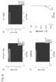
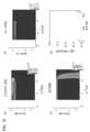
- FIG. 1is a schematic sectional view of a semiconductor device according to a first embodiment of the present invention.
- FIG. 2is a schematic plan view of FIG. 1.
- BRIEF DESCRIPTION OF THE DRAWINGSIt is explanatory drawing of the manufacturing method of the semiconductor device which concerns on the 1st Embodiment of this invention, Comprising: (a) Process drawing which forms the epitaxial layer 1 in the surface of the board
- FIG. 4Eis a process diagram in which a gate electrode 7 is formed after the gate insulating film 6 is formed.
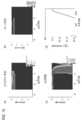
- FIG. 5Fis a process diagram in which a source electrode 9 is formed after the interlayer insulating layer 8 is formed. The figure which shows the impurity concentration of the depth direction at the time of doping by ion implantation energy 380 keV and dose amount 3.6 * 10 ⁇ 13 > cm ⁇ -2 >.
- the irradiation conditions of an impurityare 300 keV / 1.5 * 10 ⁇ 13 > cm ⁇ -2 > about the 1st step, and about the 2nd step.
- Impurity irradiation conditionsare 300 keV / 1.8 * 10 ⁇ 13 > cm ⁇ -2 > about the 1st stage, and about the 2nd stage.
- the irradiation conditions of an impurityare 250 keV / 6.0 * 10 ⁇ 12 > cm ⁇ -2 > about the 1st step, and about the 2nd step.
- the irradiation conditions of an impurityare 300 keV / 6.0 * 10 ⁇ 12 > cm ⁇ -2 > about the 1st stage, and about the 2nd stage.
- the irradiation conditions of an impurityare 250 keV / 1.2 * 10 ⁇ 13 > cm ⁇ -2 > about the 1st step, and about the 2nd step.
- the irradiation conditions of an impurityare 250 keV / 1.5 * 10 ⁇ 13 > cm ⁇ -2 > about the 1st step, and about the 2nd step.
- the irradiation conditions of an impurityare 250 keV / 1.8 * 10 ⁇ 13 > cm ⁇ -2 > about the 1st step, and about the 2nd step.
- the irradiation conditions of an impurityare 200 keV / 8.0 * 10 ⁇ 12 > cm ⁇ -2 > about the 1st step, and about the 2nd step.
- the figure in the case of 300 keV / 4.0 ⁇ 10 12 cm ⁇ 2It is a figure which shows the simulation result about the semiconductor device which concerns on the 1st Embodiment of this invention, Comprising:
- the irradiation conditions of an impurityare 200 keV / 1.2 * 10 ⁇ 13 > cm ⁇ -2 > about the 1st step, and about the 2nd step.
- FIG. 6is a schematic plan view of a semiconductor device according to a second embodiment of the present invention. The typical cross-section figure of the semiconductor device which concerns on the 3rd Embodiment of this invention.
- FIG. 6is a schematic sectional view of a conventional semiconductor device.
- the power MOSFET of the first embodimentincludes a substrate 11 made of a first main electrode region containing silicon carbide, and a first conductive made of silicon carbide laminated on the surface of the substrate 11.
- Type epitaxial layer 1first conductive type second main electrode region 5 disposed separately from the surface layer of epitaxial layer 1, and second conductive type well contact region sandwiched between second main electrode regions 5 2, a second conductive type well region 3 disposed in contact with the substrate 11 side surface of the second main electrode region 5 and the second conductive type well contact region 2, a second main electrode region 5 and a second conductive type well
- the second conductivity type well extension region 4arranged so as to sandwich the region 3 and the surface of the second conductivity type well extension region 4 sandwiched between the second main electrode region 5 and the surface exposed portion of the epitaxial layer 1 are formed on the surface.
- the second conductive type well region 3has a second conductive type impurity concentration in the depth direction from the surface of the epitaxial layer 1 toward the substrate 11. , The concentration peak position is deeper than the concentration peak position in the concentration of the second conductivity type impurity included in the second conductivity type well extension region 4.
- the main electrode regionmeans a semiconductor region located at both ends of the main current passage, and the main electrode means a main electrode such as a drain electrode or a source electrode.
- the substrate 11 made of the first main electrode regionhas the first conductivity type, the first main electrode region is a drain region, the second main electrode region 5 is a source region, and the first main electrode 10 is a drain region.
- the second main electrode 9is a source electrode.
- the first conductivity type and the second conductivity typeare opposite to each other. That is, if the first conductivity type is n-type, the second conductivity type is p-type, and if the first conductivity type is p-type, the second conductivity type is n-type. In the following, the first conductivity type is n-type, and the second conductivity type is p-type.
- Substrate 11 containing silicon carbide (SiC)is made of an n + type SiC semiconductor having a relatively high n-type impurity concentration, and an n-type SiC semiconductor epitaxial layer having an n-type impurity concentration lower than that of substrate 11 on the surface of substrate 11. 1 is arranged.
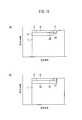
- FIG. 2is a plan view showing an example of the structure of each impurity region arranged in the surface layer of the epitaxial layer 1.
- the gate insulating film 6, the gate electrode 7, the interlayer insulating layer 8, and the source electrode 9are omitted.
- FIG. 1is a cross-sectional view of a portion along line II in FIG.
- the n + -type source region 5has a square frame shape in plan view, and the p-type well contact region 2 is disposed so as to be surrounded by the square frame of the n + -type source region 5.
- the p-type well region 3is disposed in contact with the surface of the n + -type source region 5 and the p-type well contact region 2 on the substrate 11 side, and the p-type well extension region 4 is disposed on the n + -type source region 5 and the p-type well region. It arrange
- the substrate 11 side surface of the p-type well region 3is deeper from the surface of the epitaxial layer 1 than the surface of the p-type well extension region 4 on the substrate 11 side.
- the depth from the surface of the epitaxial layer 1is 0.2 to 0.5 ⁇ m for the p-type well contact region 2, 0.05 to 0.1 ⁇ m for the n + -type source region 5, and the p-type well region 3. Is 0.2 to 0.7 ⁇ m, and the p-type well extension region 4 is 0.15 to 0.5 ⁇ m.
- the gate insulating film 6 and the gate electrode 7are sequentially stacked on the epitaxial layer 1.
- the gate insulating film 6is made of, for example, silicon oxide (SiO 2 ), and is disposed between the outer peripheral edge of the n + -type source region 5 and the outside of the p-type well extension region 4, and the n + -type source region 5.
- the surface of the epitaxial layer 1is covered between the outer peripheral edge portion and the outside of the p-type well extension region 4.
- the gate electrode 7is made of, for example, polycrystalline silicon and connected to an external electrode terminal.
- the interlayer insulating layer 8is made of, for example, SiO 2 and is disposed so as to cover the gate insulating film 6 and the gate electrode 7, and insulates the source electrode 9 and the gate electrode 7.
- the source electrode 9is made of a metal such as aluminum (Al), for example, and has a rectangular shape in plan view, for example, and is disposed on the interlayer insulating layer 8. Source electrode 9 is connected to the source contact region including the surface of the inner peripheral edge of n + -type source region 5 and the surface of p-type well contact region 2. The source contact region may be connected via a metal thin film such as Ni.
- the drain electrode 10is made of, for example, a metal such as Al, and is disposed on the back side of the substrate 11 (on the side opposite to the epitaxial layer 1) so as to entirely cover the back side of the substrate 11.
- a guard ring(not shown) containing a p-type impurity is disposed near the surface of the outer peripheral edge portion of the epitaxial layer 1.
- the concentration of the p-type impurity in the p-type well region 3is such that the concentration peak position in the depth direction from the surface of the epitaxial layer 1 toward the substrate 11 is the concentration peak in the concentration of the p-type impurity in the p-type well extension region 4. Deeper than position.
- the p-type impurity concentration of the p-type well region 3has a peak near the deepest portion (boundary portion with the epitaxial layer 1), and continuously and gradually decreases as the surface is approached.
- the peak concentration of the p-type impurity in the p-type well region 3is 2 ⁇ 10 17 to 3 ⁇ 10 18 cm ⁇ 3 , preferably 4 ⁇ 10 17 to 2 ⁇ 10 18 cm ⁇ 3 .
- the peak position of the p-type impurity concentrationis 0.3 to 0.6 ⁇ m, preferably 0.4 to 0.5 ⁇ m.
- the p-type impurity concentration of the p-type well extension region 4has a peak near the deepest portion (boundary portion with the epitaxial layer 1), and continuously and gradually decreases as the surface is approached.
- the peak concentration of the p-type impurity in the p-type well extension region 4is 1 ⁇ 10 17 to 2 ⁇ 10 18 cm ⁇ 3 , preferably 5 ⁇ 10 17 to 1 ⁇ 10 18 cm ⁇ 3 .
- the p-type impurity concentrationis 1 ⁇ 10 16 cm ⁇ 3 or less, preferably 5 ⁇ 10 15 cm ⁇ 3 or less.
- the peak position of the p-type impurity concentrationis 0.2 to 0.5 ⁇ m, preferably 0.3 to 0.4 ⁇ m.
- the p-type well contact region 2preferably has a higher average concentration of p-type impurities than the p-type well region 3 and the p-type well extension region 4. Since the average concentration of p-type impurities is high, the on-resistance is reduced.
- the operation principle of the power MOSFET according to the first embodiment of the present inventionis as follows.
- a positive voltageis applied to the gate electrode 7.
- an inversion layeris formed in the surface layer portion of the p-type well extension region 4 under the gate electrode 7, and the n + -type source region 5 and the epitaxial layer 1 are conducted through the inversion layer.
- currentcan flow from the drain electrode 10 provided on the back surface of the substrate 11 under the epitaxial layer 1 to the source electrode 9 provided on the surface of the n + -type source region 5. That is, the current can be controlled by the voltage applied to the gate electrode.
- (Production method) 3 and 4are diagrams illustrating a method for manufacturing a semiconductor device according to the first embodiment of the present invention.
- the method for manufacturing a semiconductor deviceincludes the step of forming a first conductivity type epitaxial layer 1 made of silicon carbide on the surface of a substrate 11 made of a first main electrode region containing silicon carbide. Forming a second conductivity type well extension region 4 by ion-implanting a second conductivity type impurity into the surface layer of the epitaxial layer 1 using the second conductivity type mask; and A step of forming a second conductivity type well region 3 by ion-implanting a second conductivity type impurity into the surface layer of the epitaxial layer 1 and ion implantation of the first conductivity type impurity using a first conductivity type mask. A step of forming a second main electrode region 5 of the first conductivity type.
- an epitaxial layer 1is formed by epitaxially growing the same n-type SiC semiconductor as the substrate 11 on the surface of the substrate 11 on which the n + -type SiC semiconductor is formed.
- a p-type region forming maskthat can also form a guard ring portion at the same time is used to p-type the surface layer portion of the epitaxial layer 1 by ion implantation.
- the p-type well extension region 4is formed by doping impurities with an irradiation energy of 250 keV and a dose of 1.8 ⁇ 10 13 cm ⁇ 2 .
- Examples of p-type impuritiesinclude B, Al, In, and Ga. B or Al is preferably used.
- the depth at which the p-type impurity is formedcan be controlled by adjusting the implantation energy. Further, the concentration of the p-type impurity can be controlled by adjusting the dose.
- FIGS. 5 to 9show examples of the concentration of the obtained impurity concentration in the depth direction from the surface of the epitaxial layer 1 when the implantation energy and the dose amount are changed.
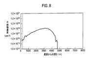
- FIG. 8is a diagram showing an example of the concentration in the depth direction of the p-type impurity of the p-type well extension region 4 obtained under the above irradiation conditions.
- the concentration peak positionis about 0.31 ⁇ m in depth from the surface of the epitaxial layer 1.
- the p-type impurity concentration at the peak positionis about 1 ⁇ 10 18 cm ⁇ 3 and about 5 ⁇ 10 15 cm ⁇ 3 near the surface.
- the p-type well region 3is formed on the surface layer of the epitaxial layer 1 using an n-type source region formation mask, for example, p-type impurities such as Al.
- the filmis formed by doping by ion implantation under an irradiation condition of an implantation energy of 380 keV and a dose of 3.6 ⁇ 10 13 cm ⁇ 2 .
- the impurity concentration of the p-type well region 3is matched, so that punch-through occurring in the vertical direction can be effectively prevented.
- the impurity concentration on the surfaceis increased, but the mobility is not affected.
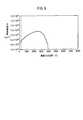
- FIG. 5is a diagram showing an example of the concentration in the depth direction of the p-type impurity of the p-type well region 3 obtained under the above irradiation conditions.
- the concentration peak positionis formed at a position where the depth from the surface of the epitaxial layer 1 is deeper than that of the p-type well extension region 4 by increasing the implantation energy. 0.48 ⁇ m.
- the p-type impurity concentration at the peak positionis about 2 ⁇ 10 18 cm ⁇ 3 .
- n + -type source regions 5are formed by ion-implanting n-type impurities by ion implantation using the same n-type source region forming mask.
- the p-type well contact region 2is formed using a p-type well contact region forming mask.
- n-type impuritiesexamples include N, P, As, and Sb. N or P is preferable.
- the surface of the epitaxial layer 1is thermally oxidized by a pyrogenic method to form a gate insulating film 6, and then subjected to a low pressure CVD (Chemical Vapor Deposition) method. Crystal silicon is formed, and the gate electrode 7 is formed using photolithography.
- CVDChemical Vapor Deposition
- a semiconductor device having a p-well structure having a two-stage structure in which the p-type well concentration region and the p-type well extension region 4 have different p-type impurity concentration peak depthscan be manufactured.
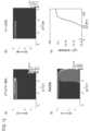
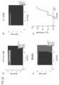
- FIGS. 11 to 20show simulation results for the semiconductor device according to the first embodiment of the present invention
- FIGS. 21 and 22show simulation results for the conventional semiconductor device.
- (A) to (c) in FIGS. 11 to 22are (a) the acceptor density distribution in two dimensions in the horizontal direction (unit: 10 ⁇ 6 m) and the depth direction (unit: 10 ⁇ 6 m), (b ) Shows the hole density distribution and (c) the current density distribution, and (d) shows that the interface between the n + -type source region 5 and the p-type well extension region 4 is zero on the horizontal axis, and the p-type well extension region starts from the interface.
- the horizontal direction to the 4th side (unit: 10 ⁇ 10 m) and the current density on the vertical axisare shown.
- FIG. 10is a diagram showing a shape model in the simulation, and FIG. 10A corresponds to the positions in the horizontal direction and the depth direction in FIGS. 11 to 20 (a) to (c).
- FIG. 10Bcorresponds to the positions in the horizontal direction and the depth direction in FIGS. 21A and 21B.
- the doping of the p-type impurity (acceptor)is performed with different implantation energy and dose amount in the first-stage p-well 4 (p-type well extension region 4) and the second-stage p-well 3 (p-type well region 3). Was performed by irradiation.
- punch-throughoccurs in the horizontal direction 45 of the first-stage p-well 4 and the vertical direction 35 of the second-stage p-well 3 even at a withstand voltage of 1200 V.
- the currentdid not flow through the epitaxial layer 1 and showed a high breakdown voltage.
- punch-throughoccurs under these impurity irradiation conditions.
- the breakdown voltage immediately before the occurrence of punch-throughis 120V in FIG. 11, 500V in FIG. 12, 700V in FIG. 13, 200V in FIG. 15, 800V in FIG. 16, 1100V in FIG. Shows pressure resistance.
- a p-well 14 of only one stageis formed with a p-type impurity (acceptor) doping irradiation condition: implantation energy 380 keV, dose amount 1.8 ⁇ 10 13 cm ⁇ 2 .
- punch-throughoccurred in the lateral direction 41 and the longitudinal direction 51 of the p-well 14 of only one stage at a withstand voltage of 500 V, and current flowed through the epitaxial layer 1.
- the p-well structurehas a two-stage structure, and the p-type impurity concentration in the deep part of the first-stage p-well 4 is high, so even when a reverse potential is applied, Punch-through occurring in the lateral direction 45 of the p-well 4 can be suppressed. Further, since the p-type impurity concentration in the deep part of the second-stage p-well 3 is high, punch-through occurring in the vertical direction 35 of the second-stage p-well 3 can be suppressed.
- the p-type impurity concentration in the vicinity of the surface of the first-stage p-well 4is low, good mobility can be ensured and the on-resistance can be reduced. Can do.
- the breakdown voltageis increased without increasing the manufacturing process.
- a structurecan be formed.
- the impurity concentration of the guard ringis set to a desired value even in the manufacturing process in which the first-stage p-well 4 is formed together with the guard ring.
- the densitycan be set.
- the pressure resistanceis improved and the manufacturing process can be simplified.
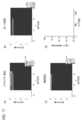
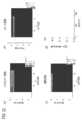
- FIG. 23is a plan view showing an example of the structure of each impurity region arranged in the surface layer of the epitaxial layer 1.
- the gate insulating film 6, the gate electrode 7, the interlayer insulating layer 8, and the source electrode 9are omitted.
- FIG. 1is a cross-sectional view taken along the line II in FIG.
- n + -type source regions 5are arranged separately from each other in plan view, and n + -type source regions 5 A p-type well contact region 2 is disposed between the two. Since other configurations are the same as those of the first embodiment, description thereof is omitted.
- the semiconductor device manufacturing method according to the second embodimentis different from the manufacturing method according to the first embodiment in the method of forming the n + -type source region 5, and the others are the same as those in the first embodiment. Since it is the same, the overlapping description is omitted.
- the pressure resistanceis improved and the manufacturing process can be simplified.
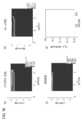
- the IGBT according to the third embodimentincludes a substrate 31 made of a first main electrode region containing silicon carbide, and a first conductivity type made of silicon carbide laminated on the surface of the substrate 31.
- a second conductivity type well region 23disposed in contact with the substrate 31 side surface of the second main electrode region 25 and the second conductivity type well contact region 22, and the second main electrode region 25 and the second conductivity type well region.
- a second conductivity type well extension region 24disposed so as to sandwich the second conductivity type well extension region 24, and a second conductivity type well extension region sandwiched between the second main electrode region 25 and the exposed surface portion of the epitaxial layer 21.
- a gate electrode 27disposed on the surface of the region 24 via a gate insulating film 26 and a second main electrode disposed in common contact with the surfaces of the second main electrode region 25 and the second conductivity type well contact region 22 29 and a first main electrode 30 disposed on the back surface opposite to the surface of the substrate 31, and the concentration of the second conductivity type impurity of the second conductivity type well region 23 is from the surface of the epitaxial layer 21 to the substrate 31.
- the concentration peak positionis deeper than the concentration peak position in the concentration of the second conductivity type impurity included in the second conductivity type well extension region 24.
- the substrate 31 formed of the first main electrode regionhas the second conductivity type, the first main electrode region is a collector region, the second main electrode region 25 is an emitter region, and the first main electrode 30 is a collector.
- the second main electrode 29is an emitter electrode.
- the first conductivity typeis n-type
- the second conductivity typeis p-type
- the substrate 31 containing silicon carbide (SiC)is made of a p + type SiC semiconductor having a relatively high p type impurity concentration, and an n type SiC semiconductor epitaxial layer 21 is disposed on the surface of the substrate 31.
- n + -type emitter region 25is arranged so as to be separated from each other in plan view, and a p-type well contact region 22 is arranged between the n + -type emitter region 25.
- the p-type well region 23is disposed in contact with the surface of the n + -type emitter region 25 and the p-type well contact region 22 on the substrate 31 side, and the p-type well extension region 24 is disposed on the n + -type emitter region 25 and the p-type well region. It arrange
- the substrate 31 side surface of the p-type well region 23is deeper from the surface of the epitaxial layer 21 than the surface of the p-type well extension region 24 on the substrate 31 side.
- the depth from the surface of the epitaxial layer 21is 0.2 to 0.5 ⁇ m for the p-type well contact region 22, 0.05 to 0.1 ⁇ m for the n + -type emitter region 25, and the p-type well region 23. 0.2 to 0.7 ⁇ m, and the p-type well extension region 24 is 0.15 to 0.5 ⁇ m.
- the gate insulating film 26 and the gate electrode 27are sequentially stacked on the epitaxial layer 21.
- the gate insulating film 26is made of, for example, silicon oxide (SiO 2 ), and is disposed between the outer peripheral edge of the n + -type emitter region 25 and the outside of the p-type well extension region 24, and the n + -type emitter region 25.
- the surface of the epitaxial layer 21is covered between the outer peripheral edge portion and the outside of the p-type well extension region 24.
- the gate electrode 27is made of, for example, polycrystalline silicon and connected to an external electrode terminal.
- the interlayer insulating layer 28is made of, for example, SiO 2 and is disposed so as to cover the gate insulating film 26 and the gate electrode 27, and insulates the emitter electrode 29 and the gate electrode 27.
- the emitter electrode 29is made of, for example, a metal such as aluminum (Al).
- the emitter electrode 29has, for example, a square shape in plan view, and is disposed on the interlayer insulating layer 28.
- the emitter electrode 29is connected to a contact region including the surface of the inner peripheral edge of the n + -type emitter region 25 and the surface of the p-type well contact region 22.
- the contact regionmay be connected via a metal thin film such as Ni.
- the collector electrode 30is made of, for example, a metal such as Al, and is disposed on the back side of the substrate 31 (on the side opposite to the epitaxial layer 21) so as to entirely cover the back side of the substrate 31.
- a guard ring(not shown) containing a p-type impurity is disposed near the surface of the outer peripheral edge portion of the epitaxial layer 21.
- the concentration of the p-type impurity in the p-type well region 23is the same as the concentration of the p-type well region 3 in the first embodiment, and the concentration of the p-type impurity in the p-type well extension region 24 is Since the concentration is the same as that of the p-type well extension region 4 in the first embodiment, the description thereof is omitted.
- a voltage higher than the emitter voltageis applied to the gate electrode 27 with a negative voltage applied to the emitter electrode 29 and a positive voltage applied to the collector electrode 30.
- an inversion layeris formed in the surface layer portion of the p-type well extension region 24 under the gate electrode 27, and electrons are injected from the emitter region 25 through the inversion layer into the substrate 31 and from the substrate 31. Holes are injected into the epitaxial layer 21.
- a currentflows from the collector electrode 30 provided on the back surface of the substrate 31 under the epitaxial layer 21 to the emitter electrode 29 provided on the surface of the emitter region 25. This current can be controlled by the voltage applied to the gate electrode 27.
- the semiconductor device manufacturing method according to the third embodimentis different from the manufacturing method according to the first embodiment in the method of forming the substrate 31, and is otherwise the same as in the first embodiment. A duplicate description is omitted.
- the pressure resistanceis improved and the manufacturing process can be simplified.
- the first conductivity typehas been described as n-type and the second conductivity type as p-type.
- the first conductivity typeis p-type and the second conductivity type. May be n-type. Also in this configuration, the same effects as those of the first to third embodiments described above can be obtained.
Landscapes
- Electrodes Of Semiconductors (AREA)
- Insulated Gate Type Field-Effect Transistor (AREA)
Abstract
Description
Translated fromJapanese本発明は、半導体装置に関し、特に、炭化シリコンを用いた半導体装置に関する。The present invention relates to a semiconductor device, and more particularly to a semiconductor device using silicon carbide.
近年、電力用半導体素子としてMOSFET(Metal Oxide Semiconductor Field Effect Transistor)やIGBT(Insulated Gate Bipolar Transistor)を用いた電力変換用半導体装置の開発が進められている。中でも、炭化シリコン(SiC)半導体を用いたものは、シリコン(Si)に比べ、SiCのバンドギャップが広く、また絶縁破壊電界が一桁も大きい等の理由から、特に注目されている。In recent years, power conversion semiconductor devices using MOSFETs (Metal Oxide Semiconductor Field Effect Transistor) and IGBTs (Insulated Gate Bipolar Transistors) as power semiconductor elements have been developed. Of these, silicon carbide (SiC) semiconductors are attracting particular attention because they have a wider SiC band gap and a single-digit larger breakdown electric field than silicon (Si).
図25に、従来のSiCを用いたパワーMOSFETの構造の一例を示す。従来のパワーMOSFETは、n+型SiC半導体基板11の表面にn-型SiC半導体エピタキシャル層1が設けられている。n-型SiC半導体エピタキシャル層1の表層部には、p型不純物領域14と、このp型不純物領域14内にp+型不純物領域2を挟んでn+型不純物領域5とが設けられている。FIG. 25 shows an example of a structure of a conventional power MOSFET using SiC. In a conventional power MOSFET, an n− type SiC semiconductor
従来、SiCでの不純物領域の形成には、Si半導体で用いられている熱拡散法による不純物領域の形成が困難であるため、通常イオン注入法が用いられている。(例えば、特許文献1参照。)。
しかし、SiCを用いたMOSFETでは、p型不純物領域14のゲート絶縁膜6との界面付近(チャネル領域)における不純物濃度が大きくなるとチャネル領域での移動度が低くなる。そのため、p型不純物領域14の表面付近の不純物濃度を低くするために、不純物イオンの注入ドーズ量を下げてp型不純物領域14の不純物濃度を全体的に低く抑える必要があった。その結果、逆電圧を印加した場合、p型不純物領域14でパンチスルーが生じる。そのため、SiC本来の絶縁破壊電界の利点を生かせず、高い耐圧を得ることができないといった問題があった。However, in the MOSFET using SiC, the mobility in the channel region decreases as the impurity concentration in the vicinity of the interface between the p-
また、ガードリングやp型不純物領域、n型不純物領域をすべて異なるマスクで形成した場合、製造プロセスが増え、歩留まりが下がるといった問題があった。Also, when the guard ring, the p-type impurity region, and the n-type impurity region are all formed with different masks, there is a problem that the manufacturing process increases and the yield decreases.
本発明の目的は、耐圧性が向上し、製造プロセスの簡易化が可能となる半導体装置を提供することにある。An object of the present invention is to provide a semiconductor device with improved pressure resistance and capable of simplifying the manufacturing process.
上記目的を達成するための本発明の一態様によれば、炭化シリコンを含む、第1主電極領域からなる基板と、前記基板の表面に積層された、炭化シリコンからなる第1導電型エピタキシャル層と、前記エピタキシャル層の表面層に互いに隔離して配置された第1導電型の第2主電極領域と、前記第2主電極領域に挟まれた第2導電型ウェルコンタクト領域と、前記第2主電極領域及び前記第2導電型ウェルコンタクト領域の前記基板側表面に接して配置された第2導電型ウェル領域と、前記第2主電極領域及び前記第2導電型ウェル領域を挟むように配置された第2導電型ウェルエクステンション領域と、前記第2主電極領域及び前記エピタキシャル層の表面露出部に挟まれた前記第2導電型ウェルエクステンション領域の表面にゲート絶縁膜を介して配置されたゲート電極と、前記第2主電極領域及び前記第2導電型ウェルコンタクト領域の表面に共通に接触して配置された第2主電極と、前記基板の表面に対向する裏面に配置された第1主電極とを備え、前記第2導電型ウェル領域が有する第2導電型不純物の濃度は、前記エピタキシャル層の表面から前記基板に向かう深さ方向において、濃度ピーク位置が、前記第2導電型ウェルエクステンション領域が有する前記第2導電型不純物の濃度における濃度ピーク位置より深いことを特徴とする半導体装置が提供される。According to one aspect of the present invention for achieving the above object, a substrate comprising silicon carbide and comprising a first main electrode region, and a first conductivity type epitaxial layer comprising silicon carbide and laminated on the surface of the substrate. A first conductive type second main electrode region disposed on the surface layer of the epitaxial layer so as to be separated from each other, a second conductive type well contact region sandwiched between the second main electrode regions, and the second A second conductive type well region disposed in contact with the substrate-side surface of the main electrode region and the second conductive type well contact region, and disposed so as to sandwich the second main electrode region and the second conductive type well region The second conductivity type well extension region formed on the surface of the second conductivity type well extension region sandwiched between the second main electrode region and the exposed surface portion of the epitaxial layer. A gate electrode disposed through a film, a second main electrode disposed in common contact with the surfaces of the second main electrode region and the second conductivity type well contact region, and a surface of the substrate A concentration of a second conductivity type impurity in the second conductivity type well region in a depth direction from the surface of the epitaxial layer toward the substrate. There is provided a semiconductor device characterized by being deeper than a concentration peak position in the concentration of the second conductivity type impurity included in the second conductivity type well extension region.
本発明によれば、耐圧性が向上し、製造プロセスの簡易化が可能となる半導体装置を提供することができる。According to the present invention, it is possible to provide a semiconductor device with improved pressure resistance and capable of simplifying the manufacturing process.
1・・・n型エピタキシャル層
2・・・p型ウェルコンタクト領域
3・・・p型ウェル領域
4・・・p型ウェルエクステンション領域
5・・・n+型ソース領域
6・・・ゲート絶縁膜
7・・・ゲート電極
8・・・層間絶縁層
9・・・ソース電極
10・・ドレイン電極
11・・基板
21・・n型エピタキシャル層
22・・p型ウェルコンタクト領域
23・・p型ウェル領域
24・・p型ウェルエクステンション領域
25・・n+型エミッタ領域
26・・ゲート絶縁膜
27・・ゲート電極
28・・層間絶縁層
29・・エミッタ電極
30・・コレクタ電極
31・・基板DESCRIPTION OF
以下、図面を参照して本発明の実施の形態による半導体装置を説明する。以下の図面の記載において、同一又は類似の部分には同一又は類似の符号を付している。ただし、図面は模式的なものであり、現実のものとは異なる。また、図面相互間においても互いの寸法の関係や比率が異なる部分が含まれていることに留意すべきである。Hereinafter, semiconductor devices according to embodiments of the present invention will be described with reference to the drawings. In the following description of the drawings, the same or similar parts are denoted by the same or similar reference numerals. However, the drawings are schematic and different from actual ones. It should also be noted that the drawings include portions having different dimensional relationships and ratios.
[第1の実施の形態]
(半導体装置の構造)
本発明の第1の実施の形態に係る半導体装置としてのパワーMOSFETについて、図1及び図2を参照して説明する。[First embodiment]
(Structure of semiconductor device)
A power MOSFET as a semiconductor device according to a first embodiment of the present invention will be described with reference to FIGS.
図1に示すように、第1の実施の形態のパワーMOSFETは、炭化シリコンを含む、第1主電極領域からなる基板11と、基板11の表面に積層された、炭化シリコンからなる第1導電型エピタキシャル層1と、エピタキシャル層1の表面層に互いに隔離して配置された第1導電型の第2主電極領域5と、第2主電極領域5に挟まれた第2導電型ウェルコンタクト領域2と、第2主電極領域5及び第2導電型ウェルコンタクト領域2の基板11側表面に接して配置された第2導電型ウェル領域3と、第2主電極領域5及び第2導電型ウェル領域3を挟むように配置された第2導電型ウェルエクステンション領域4と、第2主電極領域5及びエピタキシャル層1の表面露出部に挟まれた第2導電型ウェルエクステンション領域4の表面にゲート絶縁膜6を介して配置されたゲート電極7と、第2主電極領域5及び第2導電型ウェルコンタクト領域2の表面に共通に接触して配置された第2主電極9と、基板11の表面に対向する裏面に配置された第1主電極10とを備え、第2導電型ウェル領域3が有する第2導電型不純物の濃度は、エピタキシャル層1の表面から基板11に向かう深さ方向において、濃度ピーク位置が、第2導電型ウェルエクステンション領域4が有する第2導電型不純物の濃度における濃度ピーク位置より深い。As shown in FIG. 1, the power MOSFET of the first embodiment includes a
ここで、主電極領域とは、主電流の通路の両端に位置する半導体領域を意味し、主電極は、ドレイン電極、ソース電極等の主電極を意味する。Here, the main electrode region means a semiconductor region located at both ends of the main current passage, and the main electrode means a main electrode such as a drain electrode or a source electrode.
第1主電極領域からなる基板11は第1導電型を有しており、第1主電極領域はドレイン領域であり、第2主電極領域5はソース領域であり、第1主電極10はドレイン電極であり、第2主電極9はソース電極である。The
第1導電型と第2導電型とは互いに反対導電型である。すなわち、第1導電型がn型であれば、第2導電型はp型であり、第1導電型がp型であれば、第2導電型はn型である。以下において、第1導電型はn型であり、第2導電型はp型である。The first conductivity type and the second conductivity type are opposite to each other. That is, if the first conductivity type is n-type, the second conductivity type is p-type, and if the first conductivity type is p-type, the second conductivity type is n-type. In the following, the first conductivity type is n-type, and the second conductivity type is p-type.
炭化シリコン(SiC)を含む基板11は、n型不純物濃度が相対的に高いn+型SiC半導体からなり、基板11の表面には基板11より低いn型不純物濃度を有するn型SiC半導体エピタキシャル層1が配置されている。
図2は、エピタキシャル層1の表面層に配置された各不純物領域の構造の一例を示す平面図である。図2において、ゲート絶縁膜6、ゲート電極7、層間絶縁層8及びソース電極9は省略されている。図2のI-I線に沿う部分の断面図が図1である。FIG. 2 is a plan view showing an example of the structure of each impurity region arranged in the surface layer of the
図2に示す例では、n+型ソース領域5が平面視で四角枠状の形状を有し、p型ウェルコンタクト領域2がn+型ソース領域5の四角枠内に囲まれて配置されている。そして、p型ウェル領域3がn+型ソース領域5及びp型ウェルコンタクト領域2の基板11側表面に接して配置され、p型ウェルエクステンション領域4がn+型ソース領域5及びp型ウェル領域3の側面を挟むように配置されている。In the example shown in FIG. 2, the n+ -
p型ウェル領域3の基板11側表面は、p型ウェルエクステンション領域4の基板11側表面よりもエピタキシャル層1表面からの深さが深い。The
各領域において、エピタキシャル層1の表面からの深さは、p型ウェルコンタクト領域2が0.2~0.5μm、n+型ソース領域5が0.05~0.1μm、p型ウェル領域3が0.2~0.7μm、p型ウェルエクステンション領域4が0.15~0.5μm、を有している。In each region, the depth from the surface of the
ゲート絶縁膜6及びゲート電極7は、エピタキシャル層1の上に順に積層されている。ゲート絶縁膜6は、例えば、酸化シリコン(SiO2)からなり、n+型ソース領域5の外周縁部とp型ウェルエクステンション領域4外との間に跨って配置され、n+型ソース領域5の外周縁部とp型ウェルエクステンション領域4外との間におけるエピタキシャル層1の表面を覆っている。The
ゲート電極7は、例えば、多結晶シリコンからなり、外部電極端子と接続されている。The
層間絶縁層8は、例えば、SiO2からなり、ゲート絶縁膜6及びゲート電極7を覆うように配置されており、ソース電極9とゲート電極7を絶縁している。The interlayer insulating
ソース電極9は、例えば、アルミニウム(Al)等の金属からなり、形状は、例えば、平面視で四角形状を有しており、層間絶縁層8上に配置されている。ソース電極9は、n+型ソース領域5の内周縁部の表面とp型ウェルコンタクト領域2の表面を含むソースコンタクト領域に接続されている。Ni等の金属薄膜を介してソースコンタクト領域と接続されていてもよい。The
ドレイン電極10は、例えば、Al等の金属からなり、基板11の裏面側(エピタキシャル層1と反対側)に基板11の裏面を全体的に覆うように配置されている。The
半導体装置の耐圧を確保するために、p型不純物を含むガードリング(図示略)がエピタキシャル層1の外周縁部の表面付近に配置されているのが好ましい。In order to ensure the breakdown voltage of the semiconductor device, it is preferable that a guard ring (not shown) containing a p-type impurity is disposed near the surface of the outer peripheral edge portion of the
p型ウェル領域3が有するp型不純物の濃度は、エピタキシャル層1の表面から基板11に向かう深さ方向において、濃度ピーク位置が、p型ウェルエクステンション領域4が有するp型不純物の濃度における濃度ピーク位置より深い。The concentration of the p-type impurity in the p-
p型ウェル領域3のp型不純物濃度は、最深部(エピタキシャル層1との境界部)付近においてピークを有し、表面に近づくほど連続的かつ緩やかに低くなることが好ましい。It is preferable that the p-type impurity concentration of the p-
例えば、p型ウェル領域3のp型不純物のピーク濃度は、2×10¹⁷~3×1018cm-3、好ましくは4×10¹⁷~2×1018cm-3である。また、p型不純物濃度のピーク位置は、0.3~0.6μm、好ましくは0.4~0.5μmである。For example, the peak concentration of the p-type impurity in the p-
p型ウェルエクステンション領域4のp型不純物濃度は、最深部(エピタキシャル層1との境界部)付近においてピークを有し、表面に近づくほど連続的かつ緩やかに低くなることが好ましい。It is preferable that the p-type impurity concentration of the p-type
例えば、p型ウェルエクステンション領域4のp型不純物のピーク濃度は1×10¹⁷~2×1018cm-3、好ましくは5×10¹⁷~1×1018cm-3であり、表面付近でのp型不純物濃度は、1×1016cm-3以下、好ましくは5×1015cm-3以下である。また、p型不純物濃度のピーク位置は、0.2~0.5μm、好ましくは0.3~0.4μmである。For example, the peak concentration of the p-type impurity in the p-type
p型ウェルコンタクト領域2は、p型ウェル領域3及びp型ウェルエクステンション領域4よりもp型不純物の平均濃度が高いことが好ましい。p型不純物の平均濃度が高いことにより、オン抵抗が低減する。The p-type
(動作原理)
本発明の第1の実施の形態に係るパワーMOSFETの動作原理は以下の通りである。(Operating principle)
The operation principle of the power MOSFET according to the first embodiment of the present invention is as follows.
ゲート電極7へ正の電圧を印加する。この電圧印加により、ゲート電極7下のp型ウェルエクステンション領域4の表層部に反転層が形成され、その反転層を通じてn+型ソース領域5とエピタキシャル層1とが導通される。それにより、エピタキシャル層1の下の基板11裏面に設けられたドレイン電極10からn+型ソース領域5の表面に設けられたソース電極9へと電流を流すことができる。すなわち、ゲート電極に印加する電圧によって電流を制御することができる。A positive voltage is applied to the
(製造方法)
図3及び図4は、本発明の第1の実施の形態による半導体装置の製造方法を説明する図である。(Production method)
3 and 4 are diagrams illustrating a method for manufacturing a semiconductor device according to the first embodiment of the present invention.
本発明の第1の実施の形態に係る半導体装置の製造方法は、炭化シリコンを含む第1主電極領域からなる基板11の表面に、炭化シリコンからなる第1導電型エピタキシャル層1を形成する工程と、第2導電型用マスクを用いてエピタキシャル層1の表面層に第2導電型不純物をイオン注入することにより第2導電型ウェルエクステンション領域4を形成する工程と、第1導電型用マスクを用いてエピタキシャル層1の表面層に第2導電型不純物をイオン注入することにより第2導電型ウェル領域3を形成する工程と、第1導電型用マスクを用いて第1導電型不純物をイオン注入することにより第1導電型の第2主電極領域5を形成する工程とを有する。The method for manufacturing a semiconductor device according to the first embodiment of the present invention includes the step of forming a first conductivity
以下に、製造工程を詳述する。The manufacturing process will be described in detail below.
(a)まず、図3(a)に示すように、n+型SiC半導体が形成された基板11の表面に基板11と同じn型SiC半導体をエピタキシャル成長させてエピタキシャル層1を形成する。(A) First, as shown in FIG. 3A, an
(b)次に、図3(b)に示すように、ガードリング部も同時に形成することができるp型領域形成用マスクを用いて、エピタキシャル層1の表層部に、イオン注入法によりp型不純物を注入エネルギー250keV、ドーズ量1.8×1013cm-2の照射条件でドーピングすることによりp型ウェルエクステンション領域4を形成する。(B) Next, as shown in FIG. 3B, a p-type region forming mask that can also form a guard ring portion at the same time is used to p-type the surface layer portion of the
p型不純物としては、B,Al,In,Ga等を挙げることができる。好ましくはB若しくはAlを用いるのがよい。Examples of p-type impurities include B, Al, In, and Ga. B or Al is preferably used.
ここで、注入エネルギーを調節することにより、p型不純物の形成される深さを制御することができる。またドーズ量を調節することにより、p型不純物の濃度を制御することができる。Here, the depth at which the p-type impurity is formed can be controlled by adjusting the implantation energy. Further, the concentration of the p-type impurity can be controlled by adjusting the dose.
図5~9に、注入エネルギーとドーズ量を変えた場合において、得られた不純物濃度のエピタキシャル層1の表面からの深さ方向における濃度の例を示した。FIGS. 5 to 9 show examples of the concentration of the obtained impurity concentration in the depth direction from the surface of the
図8は、上記の照射条件で得られた、p型ウェルエクステンション領域4が有するp型不純物の深さ方向における濃度の一例を示す図である。濃度のピーク位置は、エピタキシャル層1の表面からの深さが約0.31μmである。ピーク位置でのp型不純物濃度は、約1×1018cm-3であり、表面付近では約5×1015cm-3である。FIG. 8 is a diagram showing an example of the concentration in the depth direction of the p-type impurity of the p-type
(c)次に、図3(c)に示すように、p型ウェル領域3を、n型ソース領域形成用マスクを用いてエピタキシャル層1の表面層に、例えば、p型不純物であるAlを、イオン注入法により注入エネルギー380keV、ドーズ量3.6×1013cm-2の照射条件でドーピングすることにより形成する。これにより、p型ウェル領域3では、p型ウェルエクステンション領域4の不純物濃度に加えて、p型ウェル領域3の不純物濃度が合わされるため、縦方向で起こるパンチスルーを効果的に防ぐことができる。さらに、p型ウェル領域3は、チャネル領域とは関係がないので、表面での不純物濃度は高くなるものの、移動度には影響しない。(C) Next, as shown in FIG. 3C, the p-
図5は、上記の照射条件で得られた、p型ウェル領域3が有するp型不純物の深さ方向における濃度の一例を示す図である。濃度のピーク位置は、注入エネルギーを高めたことにより、p型ウェルエクステンション領域4の場合と比べて、エピタキシャル層1の表面からの深さがより深い位置に形成されており、その深さは約0.48μmである。また、ピーク位置でのp型不純物濃度は、約2×1018cm-3である。FIG. 5 is a diagram showing an example of the concentration in the depth direction of the p-type impurity of the p-
(d)次に、図4(d)に示すように、同じn型ソース領域形成用マスクを用いて、イオン注入法によりn型不純物をイオン注入することによりn+型ソース領域5を形成する。次いで、p型ウェルコンタクト領域形成用マスクを用いてp型ウェルコンタクト領域2を形成する。(D) Next, as shown in FIG. 4D, n+ -
n型不純物としては、N,P,As,Sb等を挙げることができる。好ましくはN若しくはPであるのがよい。Examples of n-type impurities include N, P, As, and Sb. N or P is preferable.
(e)次に、図4(e)に示すように、パイロジェニック法により、エピタキシャル層1の表面を熱酸化してゲート絶縁膜6を形成した後、減圧CVD(Chemical Vapor Deposition)法により多結晶シリコンを形成し、フォトリソグラフィを用いてゲート電極7を形成する。(E) Next, as shown in FIG. 4 (e), the surface of the
(f)次に、図4(f)に示すように、パイロジェニック法により、熱酸化して層間絶縁層8を形成した後、RIE(Reactive Ion Etching)により、エピタキシャル層1の表面の電極接触部分を露出させた後、アルミニウム等を蒸着し、ソース電極9を形成する。(F) Next, as shown in FIG. 4 (f), after the interlayer insulating
(g)最後に、基板11の裏面をアルミニウム等を蒸着して、ドレイン電極10を形成して、図1に示す半導体装置が完成する。(G) Finally, aluminum or the like is deposited on the back surface of the
このような製造方法により、p型ウェル領域3とp型ウェルエクステンション領域4において、p型不純物濃度のピーク位置の深さが異なる2段構造のpウェル構造を有する半導体装置を製造することができる。By such a manufacturing method, a semiconductor device having a p-well structure having a two-stage structure in which the p-type well concentration region and the p-type
(シミュレーション)
図11~20に、本発明の第1の実施の形態に係る半導体装置についてのシミュレーション結果を示し、図21及び22に、従来の半導体装置についてのシミュレーション結果を示した。図11~22における(a)~(c)は、水平方向(単位:10-6m)及び深さ方向(単位:10-6m)の二次元における、(a)アクセプター密度分布、(b)ホール密度分布、(c)電流密度分布、を示し、(d)は、横軸にn+型ソース領域5とp型ウェルエクステンション領域4の界面をゼロとして、その界面からp型ウェルエクステンション領域4側への水平方向(単位:10-10m)、縦軸に電流密度、を示す。(simulation)
11 to 20 show simulation results for the semiconductor device according to the first embodiment of the present invention, and FIGS. 21 and 22 show simulation results for the conventional semiconductor device. (A) to (c) in FIGS. 11 to 22 are (a) the acceptor density distribution in two dimensions in the horizontal direction (unit: 10−6 m) and the depth direction (unit: 10−6 m), (b ) Shows the hole density distribution and (c) the current density distribution, and (d) shows that the interface between the n+ -
図10は、シミュレーションにおける形状モデルを示す図であり、図10(a)は、図11~20の各(a)~(c)の水平方向及び深さ方向の位置に対応している。図10(b)は、図21及び22の各(a)~(c)の水平方向及び深さ方向の位置に対応している。FIG. 10 is a diagram showing a shape model in the simulation, and FIG. 10A corresponds to the positions in the horizontal direction and the depth direction in FIGS. 11 to 20 (a) to (c). FIG. 10B corresponds to the positions in the horizontal direction and the depth direction in FIGS. 21A and 21B.
p型不純物(アクセプター)のドーピングは、1段目のpウェル4(p型ウェルエクステンション領域4)と2段目のpウェル3(p型ウェル領域3)に、それぞれ異なる注入エネルギー及びドーズ量での照射により行った。The doping of the p-type impurity (acceptor) is performed with different implantation energy and dose amount in the first-stage p-well 4 (p-type well extension region 4) and the second-stage p-well 3 (p-type well region 3). Was performed by irradiation.
上記で得られた半導体装置について、ソース-ドレイン電極間に逆電圧を印加し、これを増加させていった場合について、公知のデバイス・シミュレーション手段を用いてシミュレーションを行った。For the semiconductor device obtained above, a simulation was performed using a known device simulation means in the case where a reverse voltage was applied between the source and drain electrodes and this was increased.
図14、図17、図18及び図20に示すように、耐圧1200Vにおいても、1段目pウェル4の横方向45及び2段目pウェル3の縦方向35でのパンチスルーは発生しておらず、エピタキシャル層1に電流は流れないで、高耐圧を示した。As shown in FIGS. 14, 17, 18, and 20, punch-through occurs in the
図11、図12、図13、図15、図16及び図19に示すように、それらの不純物照射条件では、パンチスルーが発生している。しかし、パンチスルー発生直前における耐圧は、図11においては120V、図12においては500V、図13においては700V、図15においては200V、図16においては800V、図19においては1100V、であり、高耐圧を示した。As shown in FIGS. 11, 12, 13, 15, 16, and 19, punch-through occurs under these impurity irradiation conditions. However, the breakdown voltage immediately before the occurrence of punch-through is 120V in FIG. 11, 500V in FIG. 12, 700V in FIG. 13, 200V in FIG. 15, 800V in FIG. 16, 1100V in FIG. Shows pressure resistance.
一方、従来の半導体装置については、1段のみのpウェル14を、p型不純物(アクセプター)のドーピングの照射条件:注入エネルギー380keV、ドーズ量1.8×1013cm-2、で形成した半導体装置は、図21に示すように、耐圧500Vにおいて、1段のみのpウェル14の横方向41及び縦方向51でパンチスルーが発生し、エピタキシャル層1に電流が流れた。On the other hand, in the conventional semiconductor device, a p-well 14 of only one stage is formed with a p-type impurity (acceptor) doping irradiation condition: implantation energy 380 keV, dose amount 1.8 × 1013 cm−2 . In the apparatus, as shown in FIG. 21, punch-through occurred in the
なお、上記した従来の半導体装置において、ドーズ量を3.6×1013cm-2に高めた場合、図22に示すように、耐圧1200Vでもパンチスルーは発生していない。しかしながら、チャネル領域での移動度が低下した。In the conventional semiconductor device described above, when the dose is increased to 3.6 × 1013 cm−2 , punch-through does not occur even at a breakdown voltage of 1200 V as shown in FIG. However, the mobility in the channel region decreased.
本発明の第1の実施の形態によれば、pウェル構造が2段構造であり、1段目のpウェル4の深部におけるp型不純物濃度が高いので、逆電位を印加した場合においても、pウェル4の横方向45で起こるパンチスルーを抑制することができる。また、2段目のpウェル3の深部におけるp型不純物濃度が高いので、2段目のpウェル3の縦方向35で起こるパンチスルーを抑制することができる。According to the first embodiment of the present invention, the p-well structure has a two-stage structure, and the p-type impurity concentration in the deep part of the first-stage p-well 4 is high, so even when a reverse potential is applied, Punch-through occurring in the
本発明の第1の実施の形態によれば、1段目のpウェル4の表面付近でのp型不純物濃度が低いので、良好な移動度を確保することができ、オン抵抗を低減することができる。According to the first embodiment of the present invention, since the p-type impurity concentration in the vicinity of the surface of the first-stage p-well 4 is low, good mobility can be ensured and the on-resistance can be reduced. Can do.
本発明の第1の実施の形態によれば、n+型ソース領域5を形成した後、pウェル3を形成する際、共通のn型用マスクを用いるので、製造プロセスが増えることなく、耐圧構造を形成することが可能となる。According to the first embodiment of the present invention, since the common n-type mask is used when forming the p-well 3 after forming the n+ -
本発明の第1の実施の形態によれば、pウェル構造が2段構造であるので、1段目のpウェル4をガードリングと共に形成する製造プロセスにおいても、ガードリングの不純物濃度を所望の濃度に設定することが可能となる。According to the first embodiment of the present invention, since the p-well structure is a two-stage structure, the impurity concentration of the guard ring is set to a desired value even in the manufacturing process in which the first-stage p-well 4 is formed together with the guard ring. The density can be set.
本発明の第1の実施の形態に係る半導体装置によれば、耐圧性が向上し、製造プロセスの簡易化が可能となる。According to the semiconductor device according to the first embodiment of the present invention, the pressure resistance is improved and the manufacturing process can be simplified.
[第2の実施の形態]
本発明の第2の実施の形態に係る半導体装置について、図23を参照して説明する。なお、第2の実施の形態において、第1の実施の形態と同一の部分については、同一の参照符号を付して、重複した説明は省略する。[Second Embodiment]
A semiconductor device according to the second embodiment of the present invention will be described with reference to FIG. Note that in the second embodiment, the same portions as those in the first embodiment are denoted by the same reference numerals, and redundant description is omitted.
図23は、エピタキシャル層1の表面層に配置された各不純物領域の構造の一例を示す平面図である。図23において、ゲート絶縁膜6、ゲート電極7、層間絶縁層8及びソース電極9は省略されている。図23のI-I線に沿う部分の断面図が図1である。FIG. 23 is a plan view showing an example of the structure of each impurity region arranged in the surface layer of the
本発明の第2の実施の形態に係る半導体装置は、図23に示すように、平面視で四角形状のn+型ソース領域5が互いに隔離して配置されており、n+型ソース領域5に挟まれてp型ウェルコンタクト領域2が配置されている。その他の構成は、第1の実施の形態と同様であるので説明は省略する。In the semiconductor device according to the second embodiment of the present invention, as shown in FIG. 23, square n+ -
第2の実施の形態に係る半導体装置の製造方法は、n+型ソース領域5を形成する方法が第1の実施の形態における製造方法と異なる点であり、他は第1の実施の形態と同様であるので、重複した説明は省略する。The semiconductor device manufacturing method according to the second embodiment is different from the manufacturing method according to the first embodiment in the method of forming the n+ -
本発明の第2の実施の形態に係る半導体装置によれば、耐圧性が向上し、製造プロセスの簡易化が可能となる。According to the semiconductor device according to the second embodiment of the present invention, the pressure resistance is improved and the manufacturing process can be simplified.
[第3の実施の形態]
(半導体装置の構造)
本発明の第3の実施の形態に係る半導体装置としてのIGBTについて、図24を参照して説明する。なお、第3の実施の形態において、第1の実施の形態と同一の部分については、同一の参照符号を付して、重複した説明は省略する。[Third embodiment]
(Structure of semiconductor device)
An IGBT as a semiconductor device according to the third embodiment of the present invention will be described with reference to FIG. Note that in the third embodiment, the same portions as those in the first embodiment are denoted by the same reference numerals, and a duplicate description is omitted.
図24に示すように、第3の実施の形態のIGBTは、炭化シリコンを含む、第1主電極領域からなる基板31と、基板31の表面に積層された、炭化シリコンからなる第1導電型エピタキシャル層21と、エピタキシャル層21の表面層に互いに隔離して配置された第1導電型の第2主電極領域25と、第2主電極領域25に挟まれた第2導電型ウェルコンタクト領域22と、第2主電極領域25及び第2導電型ウェルコンタクト領域22の基板31側表面に接して配置された第2導電型ウェル領域23と、第2主電極領域25及び第2導電型ウェル領域23を挟むように配置された第2導電型ウェルエクステンション領域24と、第2主電極領域25及びエピタキシャル層21の表面露出部に挟まれた第2導電型ウェルエクステンション領域24の表面にゲート絶縁膜26を介して配置されたゲート電極27と、第2主電極領域25及び第2導電型ウェルコンタクト領域22の表面に共通に接触して配置された第2主電極29と、基板31の表面に対向する裏面に配置された第1主電極30とを備え、第2導電型ウェル領域23が有する第2導電型不純物の濃度は、エピタキシャル層21の表面から基板31に向かう深さ方向において、濃度ピーク位置が、第2導電型ウェルエクステンション領域24が有する第2導電型不純物の濃度における濃度ピーク位置より深い。As shown in FIG. 24, the IGBT according to the third embodiment includes a
第1主電極領域からなる基板31は第2導電型を有しており、第1主電極領域はコレクタ領域であり、第2主電極領域25はエミッタ領域であり、第1主電極30はコレクタ電極であり、第2主電極29はエミッタ電極である。The
以下において、第1導電型はn型であり、第2導電型はp型である。In the following, the first conductivity type is n-type, and the second conductivity type is p-type.
炭化シリコン(SiC)を含む基板31は、p型不純物濃度が相対的に高いp+型SiC半導体からなり、基板31の表面にはn型SiC半導体エピタキシャル層21が配置されている。The
エピタキシャル層21の表面層には、平面視で四角形状のn+型エミッタ領域25が互いに隔離して配置されており、n+型エミッタ領域25に挟まれてp型ウェルコンタクト領域22が配置されている。そして、p型ウェル領域23がn+型エミッタ領域25及びp型ウェルコンタクト領域22の基板31側表面に接して配置され、p型ウェルエクステンション領域24がn+型エミッタ領域25及びp型ウェル領域23の側面を挟むように配置されている。On the surface layer of the
p型ウェル領域23の基板31側表面は、p型ウェルエクステンション領域24の基板31側表面よりもエピタキシャル層21表面からの深さが深い。The
各領域において、エピタキシャル層21の表面からの深さは、p型ウェルコンタクト領域22が0.2~0.5μm、n+型エミッタ領域25が0.05~0.1μm、p型ウェル領域23が0.2~0.7μm、p型ウェルエクステンション領域24が0.15~0.5μm、を有している。In each region, the depth from the surface of the
ゲート絶縁膜26及びゲート電極27は、エピタキシャル層21の上に順に積層されている。ゲート絶縁膜26は、例えば、酸化シリコン(SiO2)からなり、n+型エミッタ領域25の外周縁部とp型ウェルエクステンション領域24外との間に跨って配置され、n+型エミッタ領域25の外周縁部とp型ウェルエクステンション領域24外との間におけるエピタキシャル層21の表面を覆っている。The
ゲート電極27は、例えば、多結晶シリコンからなり、外部電極端子と接続されている。The
層間絶縁層28は、例えば、SiO2からなり、ゲート絶縁膜26及びゲート電極27を覆うように配置されており、エミッタ電極29とゲート電極27を絶縁している。The interlayer insulating
エミッタ電極29は、例えば、アルミニウム(Al)等の金属からなり、形状は、例えば、平面視で四角形状を有しており、層間絶縁層28上に配置されている。エミッタ電極29は、n+型エミッタ領域25の内周縁部の表面とp型ウェルコンタクト領域22の表面を含むコンタクト領域に接続されている。Ni等の金属薄膜を介してコンタクト領域と接続されていてもよい。The
コレクタ電極30は、例えば、Al等の金属からなり、基板31の裏面側(エピタキシャル層21と反対側)に基板31の裏面を全体的に覆うように配置されている。The
半導体装置の耐圧を確保するために、p型不純物を含むガードリング(図示略)がエピタキシャル層21の外周縁部の表面付近に配置されているのが好ましい。In order to ensure the breakdown voltage of the semiconductor device, it is preferable that a guard ring (not shown) containing a p-type impurity is disposed near the surface of the outer peripheral edge portion of the
p型ウェル領域23が有するp型不純物の濃度は、第1の実施の形態におけるp型ウェル領域3の濃度と同様であり、またp型ウェルエクステンション領域24が有するp型不純物の濃度は、第1の実施の形態におけるp型ウェルエクステンション領域4の濃度と同様であるので、説明を省略する。The concentration of the p-type impurity in the p-
(動作原理)
本発明の第3の実施の形態に係るIGBTの動作原理は以下の通りである。(Operating principle)
The operation principle of the IGBT according to the third embodiment of the present invention is as follows.
エミッタ電極29に負の電圧、コレクタ電極30に正の電圧を印加した状態で、ゲート電極27にエミッタ電圧より高い電圧を印加する。この電圧印加により、ゲート電極27下のp型ウェルエクステンション領域24の表層部に反転層が形成され、電子がエミッタ領域25から反転層を介して、基板31に注入されると共に、基板31から正孔がエピタキシャル層21へ注入される。これにより、エピタキシャル層21の下の基板31裏面に設けられたコレクタ電極30からエミッタ領域25の表面に設けられたエミッタ電極29へと電流が流れる。この電流は、ゲート電極27に印加する電圧によって制御することができる。A voltage higher than the emitter voltage is applied to the
第3の実施の形態に係る半導体装置の製造方法は、基板31を形成する方法が第1の実施の形態における製造方法と異なる点であり、他は第1の実施の形態と同様であるので、重複した説明は省略する。The semiconductor device manufacturing method according to the third embodiment is different from the manufacturing method according to the first embodiment in the method of forming the
本発明の第3の実施の形態に係る半導体装置によれば、耐圧性が向上し、製造プロセスの簡易化が可能となる。According to the semiconductor device according to the third embodiment of the present invention, the pressure resistance is improved and the manufacturing process can be simplified.
[その他の実施の形態]
以上、上述した第1乃至第3の実施の形態によって本発明を詳細に説明したが、当業者にとっては、本発明が本明細書中に説明した第1乃至第3の実施の形態に限定されるものではないということは明らかである。本発明は、特許請求の範囲の記載により定まる本発明の趣旨及び範囲を逸脱することなく修正及び変更形態として実施することができる。従って、本明細書の記載は、例示説明を目的とするものであり、本発明に対して何ら制限的な意味を有するものではない。以下、上述した第1乃至第3の実施の形態を一部変更した変更形態について説明する。[Other embodiments]
As described above, the present invention has been described in detail according to the above-described first to third embodiments. However, for those skilled in the art, the present invention is limited to the first to third embodiments described in this specification. Obviously it is not. The present invention can be implemented as modifications and changes without departing from the spirit and scope of the present invention defined by the description of the scope of claims. Therefore, the description of the present specification is for illustrative purposes and does not have any limiting meaning to the present invention. Hereinafter, modified embodiments in which the first to third embodiments described above are partially modified will be described.
上述した第1乃至第3の実施の形態に係る半導体装置において、第1導電型をn型、第2導電型をp型として説明をしたが、第1導電型をp型、第2導電型をn型としてもよい。この構成においても、それぞれ上述した第1乃至第3の実施の形態と同様の効果が得られる。In the semiconductor devices according to the first to third embodiments described above, the first conductivity type has been described as n-type and the second conductivity type as p-type. However, the first conductivity type is p-type and the second conductivity type. May be n-type. Also in this configuration, the same effects as those of the first to third embodiments described above can be obtained.
Claims (5)
Translated fromJapanese前記基板の表面に積層された、炭化シリコンからなる第1導電型エピタキシャル層と、
前記エピタキシャル層の表面層に互いに隔離して配置された第1導電型の第2主電極領域と、
前記第2主電極領域に挟まれた第2導電型ウェルコンタクト領域と、
前記第2主電極領域及び前記第2導電型ウェルコンタクト領域の前記基板側表面に接して配置された第2導電型ウェル領域と、
前記第2主電極領域及び前記第2導電型ウェル領域を挟むように配置された第2導電型ウェルエクステンション領域と、
前記第2主電極領域及び前記エピタキシャル層の表面露出部に挟まれた前記第2導電型ウェルエクステンション領域の表面にゲート絶縁膜を介して配置されたゲート電極と、
前記第2主電極領域及び前記第2導電型ウェルコンタクト領域の表面に共通に接触して配置された第2主電極と、
前記基板の表面に対向する裏面に配置された第1主電極とを備え、
前記第2導電型ウェル領域が有する第2導電型不純物の濃度は、前記エピタキシャル層の表面から前記基板に向かう深さ方向において、濃度ピーク位置が、前記第2導電型ウェルエクステンション領域が有する前記第2導電型不純物の濃度における濃度ピーク位置より深いことを特徴とする半導体装置。A substrate comprising a first main electrode region comprising silicon carbide;
A first conductivity type epitaxial layer made of silicon carbide, laminated on the surface of the substrate;
A second main electrode region of a first conductivity type disposed on the surface layer of the epitaxial layer and separated from each other;
A second conductivity type well contact region sandwiched between the second main electrode regions;
A second conductivity type well region disposed in contact with the substrate side surface of the second main electrode region and the second conductivity type well contact region;
A second conductivity type well extension region disposed so as to sandwich the second main electrode region and the second conductivity type well region;
A gate electrode disposed on a surface of the second conductivity type well extension region sandwiched between the second main electrode region and the surface exposed portion of the epitaxial layer via a gate insulating film;
A second main electrode disposed in common contact with the surfaces of the second main electrode region and the second conductivity type well contact region;
A first main electrode disposed on the back surface facing the front surface of the substrate,
The concentration of the second conductivity type impurity in the second conductivity type well region is such that the concentration peak position in the depth direction from the surface of the epitaxial layer toward the substrate is the second conductivity type well extension region. A semiconductor device characterized by being deeper than a concentration peak position in the concentration of two conductivity type impurities.
Priority Applications (4)
| Application Number | Priority Date | Filing Date | Title |
|---|---|---|---|
| CN2009801044409ACN101939843B (en) | 2008-02-06 | 2009-02-06 | Semiconductor device |
| EP09707543AEP2242107A4 (en) | 2008-02-06 | 2009-02-06 | SEMICONDUCTOR DEVICE |
| JP2009552537AJP5693851B2 (en) | 2008-02-06 | 2009-02-06 | Semiconductor device |
| US12/866,528US20110012132A1 (en) | 2008-02-06 | 2009-02-06 | Semiconductor Device |
Applications Claiming Priority (2)
| Application Number | Priority Date | Filing Date | Title |
|---|---|---|---|
| JP2008026973 | 2008-02-06 | ||
| JP2008-026973 | 2008-02-06 |
Publications (1)
| Publication Number | Publication Date |
|---|---|
| WO2009099182A1true WO2009099182A1 (en) | 2009-08-13 |
Family
ID=40952254
Family Applications (1)
| Application Number | Title | Priority Date | Filing Date |
|---|---|---|---|
| PCT/JP2009/052050WO2009099182A1 (en) | 2008-02-06 | 2009-02-06 | Semiconductor device |
Country Status (5)
| Country | Link |
|---|---|
| US (1) | US20110012132A1 (en) |
| EP (1) | EP2242107A4 (en) |
| JP (2) | JP5693851B2 (en) |
| CN (2) | CN101939843B (en) |
| WO (1) | WO2009099182A1 (en) |
Cited By (7)
| Publication number | Priority date | Publication date | Assignee | Title |
|---|---|---|---|---|
| JP2012059744A (en)* | 2010-09-06 | 2012-03-22 | Toshiba Corp | Semiconductor device |
| CN102544091A (en)* | 2010-12-17 | 2012-07-04 | 浙江大学 | Novel silicon carbide MOSFET (Metal Oxide Semiconductor Field Effect Transistor) |
| JP2012129492A (en)* | 2010-11-26 | 2012-07-05 | Mitsubishi Electric Corp | Silicon carbide semiconductor device and method of manufacturing the same |
| JP2013179361A (en)* | 2013-06-13 | 2013-09-09 | Mitsubishi Electric Corp | Semiconductor device |
| JP2014225713A (en)* | 2010-04-26 | 2014-12-04 | 三菱電機株式会社 | Semiconductor device |
| CN106098539A (en)* | 2009-09-07 | 2016-11-09 | 罗姆股份有限公司 | Semiconductor device |
| EP3920237B1 (en)* | 2010-09-17 | 2025-04-09 | Rohm Co., Ltd. | Semiconductor device |
Families Citing this family (13)
| Publication number | Priority date | Publication date | Assignee | Title |
|---|---|---|---|---|
| US8674439B2 (en) | 2010-08-02 | 2014-03-18 | Microsemi Corporation | Low loss SiC MOSFET |
| JP5621621B2 (en) | 2011-01-24 | 2014-11-12 | 三菱電機株式会社 | Semiconductor device and method for manufacturing semiconductor device |
| US9029945B2 (en) | 2011-05-06 | 2015-05-12 | Cree, Inc. | Field effect transistor devices with low source resistance |
| US9673283B2 (en) | 2011-05-06 | 2017-06-06 | Cree, Inc. | Power module for supporting high current densities |
| US9142662B2 (en)* | 2011-05-06 | 2015-09-22 | Cree, Inc. | Field effect transistor devices with low source resistance |
| JP5995435B2 (en) | 2011-08-02 | 2016-09-21 | ローム株式会社 | Semiconductor device and manufacturing method thereof |
| US9640617B2 (en) | 2011-09-11 | 2017-05-02 | Cree, Inc. | High performance power module |
| US9373617B2 (en) | 2011-09-11 | 2016-06-21 | Cree, Inc. | High current, low switching loss SiC power module |
| WO2014204491A1 (en)* | 2013-06-21 | 2014-12-24 | Microsemi Corporation | Low loss sic mosfet |
| US10192958B2 (en)* | 2014-06-24 | 2019-01-29 | General Electric Company | Cellular layout for semiconductor devices |
| JP6523887B2 (en)* | 2015-09-11 | 2019-06-05 | 株式会社東芝 | Semiconductor device |
| DE112017008299T5 (en)* | 2017-12-21 | 2020-10-15 | Mitsubishi Electric Corporation | SEMI-CONDUCTOR UNIT |
| US20210399128A1 (en)* | 2020-06-19 | 2021-12-23 | Cree, Inc. | Power devices with a hybrid gate structure |
Citations (5)
| Publication number | Priority date | Publication date | Assignee | Title |
|---|---|---|---|---|
| JPS61283169A (en)* | 1985-06-10 | 1986-12-13 | Tdk Corp | Vertical field effect transistor and its manufacturing method |
| JPH03192772A (en)* | 1989-12-21 | 1991-08-22 | Nec Corp | Field effect transistor |
| JPH05259443A (en)* | 1992-01-16 | 1993-10-08 | Fuji Electric Co Ltd | Insulation gate type semiconductor device |
| JP2000077662A (en)* | 1998-09-02 | 2000-03-14 | Hitachi Ltd | Semiconductor switching element |
| JP2006303272A (en)* | 2005-04-22 | 2006-11-02 | Mitsubishi Electric Corp | Semiconductor device and manufacturing method thereof |
Family Cites Families (11)
| Publication number | Priority date | Publication date | Assignee | Title |
|---|---|---|---|---|
| EP0696054B1 (en)* | 1994-07-04 | 2002-02-20 | STMicroelectronics S.r.l. | Process for the manufacturing of high-density MOS-technology power devices |
| JP3279151B2 (en)* | 1995-10-23 | 2002-04-30 | トヨタ自動車株式会社 | Semiconductor device and manufacturing method thereof |
| EP0772241B1 (en)* | 1995-10-30 | 2004-06-09 | STMicroelectronics S.r.l. | High density MOS technology power device |
| JP3240896B2 (en)* | 1995-11-21 | 2001-12-25 | 富士電機株式会社 | MOS type semiconductor device |
| US6049104A (en)* | 1997-11-28 | 2000-04-11 | Magepower Semiconductor Corp. | MOSFET device to reduce gate-width without increasing JFET resistance |
| JP4123636B2 (en)* | 1998-06-22 | 2008-07-23 | 株式会社デンソー | Silicon carbide semiconductor device and manufacturing method thereof |
| JP3428459B2 (en)* | 1998-09-01 | 2003-07-22 | 富士電機株式会社 | Silicon carbide n-channel MOS semiconductor device and method of manufacturing the same |
| JP4696335B2 (en)* | 2000-05-30 | 2011-06-08 | 株式会社デンソー | Semiconductor device and manufacturing method thereof |
| JP3997886B2 (en)* | 2002-10-22 | 2007-10-24 | 日産自動車株式会社 | Method for manufacturing silicon carbide semiconductor device |
| US7074643B2 (en)* | 2003-04-24 | 2006-07-11 | Cree, Inc. | Silicon carbide power devices with self-aligned source and well regions and methods of fabricating same |
| JP5155536B2 (en)* | 2006-07-28 | 2013-03-06 | 一般財団法人電力中央研究所 | Method for improving the quality of SiC crystal and method for manufacturing SiC semiconductor device |
- 2009
- 2009-02-06EPEP09707543Apatent/EP2242107A4/ennot_activeWithdrawn
- 2009-02-06CNCN2009801044409Apatent/CN101939843B/enactiveActive
- 2009-02-06JPJP2009552537Apatent/JP5693851B2/enactiveActive
- 2009-02-06CNCN201210278267.8Apatent/CN102820338B/enactiveActive
- 2009-02-06USUS12/866,528patent/US20110012132A1/ennot_activeAbandoned
- 2009-02-06WOPCT/JP2009/052050patent/WO2009099182A1/enactiveApplication Filing
- 2015
- 2015-02-04JPJP2015019972Apatent/JP6055498B2/enactiveActive
Patent Citations (5)
| Publication number | Priority date | Publication date | Assignee | Title |
|---|---|---|---|---|
| JPS61283169A (en)* | 1985-06-10 | 1986-12-13 | Tdk Corp | Vertical field effect transistor and its manufacturing method |
| JPH03192772A (en)* | 1989-12-21 | 1991-08-22 | Nec Corp | Field effect transistor |
| JPH05259443A (en)* | 1992-01-16 | 1993-10-08 | Fuji Electric Co Ltd | Insulation gate type semiconductor device |
| JP2000077662A (en)* | 1998-09-02 | 2000-03-14 | Hitachi Ltd | Semiconductor switching element |
| JP2006303272A (en)* | 2005-04-22 | 2006-11-02 | Mitsubishi Electric Corp | Semiconductor device and manufacturing method thereof |
Cited By (17)
| Publication number | Priority date | Publication date | Assignee | Title |
|---|---|---|---|---|
| US11296223B2 (en) | 2009-09-07 | 2022-04-05 | Rohm Co., Ltd. | Semiconductor device |
| US11610992B2 (en) | 2009-09-07 | 2023-03-21 | Rohm Co., Ltd. | Semiconductor device |
| US12439634B2 (en) | 2009-09-07 | 2025-10-07 | Rohm Co., Ltd. | Semiconductor device |
| US11777030B2 (en) | 2009-09-07 | 2023-10-03 | Rohm Co., Ltd. | Semiconductor device |
| US10804392B2 (en) | 2009-09-07 | 2020-10-13 | Rohm Co., Ltd. | Semiconductor device |
| US11043589B2 (en) | 2009-09-07 | 2021-06-22 | Rohm Co., Ltd. | Semiconductor device |
| CN106098539A (en)* | 2009-09-07 | 2016-11-09 | 罗姆股份有限公司 | Semiconductor device |
| US10319853B2 (en) | 2009-09-07 | 2019-06-11 | Rohm Co., Ltd. | Semiconductor device |
| US10546954B2 (en) | 2009-09-07 | 2020-01-28 | Rohm Co., Ltd. | Semiconductor device |
| US10062758B2 (en) | 2010-04-26 | 2018-08-28 | Mitsubishi Electric Corporation | Semiconductor device |
| JP2014225713A (en)* | 2010-04-26 | 2014-12-04 | 三菱電機株式会社 | Semiconductor device |
| JP2012059744A (en)* | 2010-09-06 | 2012-03-22 | Toshiba Corp | Semiconductor device |
| EP3920237B1 (en)* | 2010-09-17 | 2025-04-09 | Rohm Co., Ltd. | Semiconductor device |
| US8932944B2 (en) | 2010-11-26 | 2015-01-13 | Mitsubishi Electric Corporation | Silicon carbide semiconductor device manufacturing method |
| JP2012129492A (en)* | 2010-11-26 | 2012-07-05 | Mitsubishi Electric Corp | Silicon carbide semiconductor device and method of manufacturing the same |
| CN102544091A (en)* | 2010-12-17 | 2012-07-04 | 浙江大学 | Novel silicon carbide MOSFET (Metal Oxide Semiconductor Field Effect Transistor) |
| JP2013179361A (en)* | 2013-06-13 | 2013-09-09 | Mitsubishi Electric Corp | Semiconductor device |
Also Published As
| Publication number | Publication date |
|---|---|
| JPWO2009099182A1 (en) | 2011-05-26 |
| CN101939843B (en) | 2012-09-26 |
| EP2242107A4 (en) | 2012-04-25 |
| JP6055498B2 (en) | 2016-12-27 |
| CN102820338A (en) | 2012-12-12 |
| CN101939843A (en) | 2011-01-05 |
| JP2015109472A (en) | 2015-06-11 |
| CN102820338B (en) | 2016-05-11 |
| JP5693851B2 (en) | 2015-04-01 |
| US20110012132A1 (en) | 2011-01-20 |
| EP2242107A1 (en) | 2010-10-20 |
Similar Documents
| Publication | Publication Date | Title |
|---|---|---|
| JP5693851B2 (en) | Semiconductor device | |
| US8658503B2 (en) | Semiconductor device and method of fabricating the same | |
| JP4938157B2 (en) | Semiconductor device and manufacturing method thereof | |
| CN104285301B (en) | Semiconductor device and its manufacture method | |
| WO2010125661A1 (en) | Semiconductor device and method for manufacturing the same | |
| WO2013001677A1 (en) | Semiconductor device and method for manufacturing same | |
| WO2012165329A1 (en) | Trench gate power semiconductor device and method for manufacturing same | |
| JP2006066439A (en) | Semiconductor device and manufacturing method thereof | |
| WO2014207793A1 (en) | Semiconductor device, and method for manufacturing same | |
| JP4842527B2 (en) | Manufacturing method of semiconductor device | |
| WO2014083771A1 (en) | Semiconductor element and method for manufacturing same | |
| WO2017138221A1 (en) | Silicon carbide semiconductor device and method for manufacturing same | |
| JP2012064741A (en) | Semiconductor device and method of manufacturing the same | |
| TWI605586B (en) | Lateral double-diffused metal oxide semiconductor device and method of manufacturing same | |
| JP5221976B2 (en) | Semiconductor device and manufacturing method thereof | |
| JP2009290140A (en) | Power semiconductor device and method for manufacturing the same | |
| CN100561751C (en) | Non-negative resistance LDMOS device structure and its production method | |
| JP5520024B2 (en) | Semiconductor device and manufacturing method thereof | |
| JP2004022769A (en) | Horizontal high voltage semiconductor device | |
| JP5059989B1 (en) | Semiconductor device and manufacturing method thereof | |
| JP2012104581A (en) | Semiconductor device and method of manufacturing the same | |
| JP6822088B2 (en) | Silicon Carbide Semiconductor Device and Method for Manufacturing Silicon Carbide Semiconductor Device | |
| CN106486546B (en) | Lateral double-diffused metal oxide semiconductor element and manufacturing method thereof | |
| JP2009194292A (en) | Semiconductor device and manufacturing method thereof | |
| JP5046886B2 (en) | Semiconductor device |
Legal Events
| Date | Code | Title | Description |
|---|---|---|---|
| WWE | Wipo information: entry into national phase | Ref document number:200980104440.9 Country of ref document:CN | |
| 121 | Ep: the epo has been informed by wipo that ep was designated in this application | Ref document number:09707543 Country of ref document:EP Kind code of ref document:A1 | |
| WWE | Wipo information: entry into national phase | Ref document number:2009552537 Country of ref document:JP | |
| WWE | Wipo information: entry into national phase | Ref document number:12866528 Country of ref document:US | |
| NENP | Non-entry into the national phase | Ref country code:DE | |
| WWE | Wipo information: entry into national phase | Ref document number:2009707543 Country of ref document:EP |