WO2005076380A2 - Oleds utilizing multidentate ligand systems - Google Patents
Oleds utilizing multidentate ligand systemsDownload PDFInfo
- Publication number
- WO2005076380A2 WO2005076380A2PCT/US2005/003107US2005003107WWO2005076380A2WO 2005076380 A2WO2005076380 A2WO 2005076380A2US 2005003107 WUS2005003107 WUS 2005003107WWO 2005076380 A2WO2005076380 A2WO 2005076380A2
- Authority
- WO
- WIPO (PCT)
- Prior art keywords
- group
- formula
- bidentate
- aryl
- alkyl
- Prior art date
Links
- 239000003446ligandSubstances0.000titleclaimsabstractdescription266
- 239000000463materialSubstances0.000claimsabstractdescription144
- 229910052751metalInorganic materials0.000claimsabstractdescription79
- 239000002184metalSubstances0.000claimsabstractdescription78
- 125000005647linker groupChemical group0.000claimsabstractdescription72
- 239000012044organic layerSubstances0.000claimsabstractdescription43
- 125000002524organometallic groupChemical group0.000claimsabstractdescription12
- 125000003118aryl groupChemical group0.000claimsdescription109
- 150000001875compoundsChemical class0.000claimsdescription69
- 125000000217alkyl groupChemical group0.000claimsdescription67
- 125000003710aryl alkyl groupChemical group0.000claimsdescription48
- 125000001072heteroaryl groupChemical group0.000claimsdescription42
- 125000005843halogen groupChemical group0.000claimsdescription33
- 125000003342alkenyl groupChemical group0.000claimsdescription30
- 125000000304alkynyl groupChemical group0.000claimsdescription29
- 229910052757nitrogenInorganic materials0.000claimsdescription23
- 125000006413ring segmentChemical group0.000claimsdescription22
- 229910052799carbonInorganic materials0.000claimsdescription21
- 125000000753cycloalkyl groupChemical group0.000claimsdescription21
- 125000001424substituent groupChemical group0.000claimsdescription19
- 229910052723transition metalInorganic materials0.000claimsdescription19
- 150000003624transition metalsChemical class0.000claimsdescription19
- IJGRMHOSHXDMSA-UHFFFAOYSA-NAtomic nitrogenChemical groupN#NIJGRMHOSHXDMSA-UHFFFAOYSA-N0.000claimsdescription18
- -1cycloheteroalkylChemical group0.000claimsdescription17
- OKTJSMMVPCPJKN-UHFFFAOYSA-NCarbonChemical group[C]OKTJSMMVPCPJKN-UHFFFAOYSA-N0.000claimsdescription15
- 125000001997phenyl groupChemical group[H]C1=C([H])C([H])=C(*)C([H])=C1[H]0.000claimsdescription15
- 125000000623heterocyclic groupChemical group0.000claimsdescription14
- 125000004429atomChemical group0.000claimsdescription11
- 125000004122cyclic groupChemical group0.000claimsdescription11
- 229910052741iridiumInorganic materials0.000claimsdescription9
- 125000006615aromatic heterocyclic groupChemical group0.000claimsdescription8
- 229910052763palladiumInorganic materials0.000claimsdescription8
- 125000004433nitrogen atomChemical groupN*0.000claimsdescription7
- 229910052697platinumInorganic materials0.000claimsdescription7
- 229910052787antimonyInorganic materials0.000claimsdescription6
- 229910052797bismuthInorganic materials0.000claimsdescription6
- 150000004696coordination complexChemical class0.000claimsdescription6
- 229910052745leadInorganic materials0.000claimsdescription6
- 229910052702rheniumInorganic materials0.000claimsdescription6
- 229910052703rhodiumInorganic materials0.000claimsdescription6
- 229910052709silverInorganic materials0.000claimsdescription6
- 229910052718tinInorganic materials0.000claimsdescription6
- 229910052738indiumInorganic materials0.000claimsdescription5
- 125000004076pyridyl groupChemical group0.000claimsdescription5
- 230000021615conjugationEffects0.000claims2
- 239000010410layerSubstances0.000description134
- 239000002019doping agentSubstances0.000description87
- XEKOWRVHYACXOJ-UHFFFAOYSA-NEthyl acetateChemical compoundCCOC(C)=OXEKOWRVHYACXOJ-UHFFFAOYSA-N0.000description44
- YMWUJEATGCHHMB-UHFFFAOYSA-NDichloromethaneChemical compoundClCClYMWUJEATGCHHMB-UHFFFAOYSA-N0.000description39
- VLKZOEOYAKHREP-UHFFFAOYSA-Nn-HexaneChemical classCCCCCCVLKZOEOYAKHREP-UHFFFAOYSA-N0.000description35
- 239000000203mixtureSubstances0.000description34
- XCJYREBRNVKWGJ-UHFFFAOYSA-Ncopper(II) phthalocyanineChemical compound[Cu+2].C12=CC=CC=C2C(N=C2[N-]C(C3=CC=CC=C32)=N2)=NC1=NC([C]1C=CC=CC1=1)=NC=1N=C1[C]3C=CC=CC3=C2[N-]1XCJYREBRNVKWGJ-UHFFFAOYSA-N0.000description32
- VFUDMQLBKNMONU-UHFFFAOYSA-N9-[4-(4-carbazol-9-ylphenyl)phenyl]carbazoleChemical compoundC12=CC=CC=C2C2=CC=CC=C2N1C1=CC=C(C=2C=CC(=CC=2)N2C3=CC=CC=C3C3=CC=CC=C32)C=C1VFUDMQLBKNMONU-UHFFFAOYSA-N0.000description27
- UFVXQDWNSAGPHN-UHFFFAOYSA-Kbis[(2-methylquinolin-8-yl)oxy]-(4-phenylphenoxy)alumaneChemical compound[Al+3].C1=CC=C([O-])C2=NC(C)=CC=C21.C1=CC=C([O-])C2=NC(C)=CC=C21.C1=CC([O-])=CC=C1C1=CC=CC=C1UFVXQDWNSAGPHN-UHFFFAOYSA-K0.000description27
- 239000000047productSubstances0.000description26
- 239000002904solventSubstances0.000description25
- 238000002347injectionMethods0.000description24
- 239000007924injectionSubstances0.000description24
- 239000000758substrateSubstances0.000description24
- 230000032258transportEffects0.000description24
- VQGHOUODWALEFC-UHFFFAOYSA-N2-phenylpyridineChemical compoundC1=CC=CC=C1C1=CC=CC=N1VQGHOUODWALEFC-UHFFFAOYSA-N0.000description22
- OKKJLVBELUTLKV-UHFFFAOYSA-NMethanolChemical compoundOCOKKJLVBELUTLKV-UHFFFAOYSA-N0.000description21
- 238000002390rotary evaporationMethods0.000description18
- 235000019439ethyl acetateNutrition0.000description17
- TVIVIEFSHFOWTE-UHFFFAOYSA-Ktri(quinolin-8-yloxy)alumaneChemical compound[Al+3].C1=CN=C2C([O-])=CC=CC2=C1.C1=CN=C2C([O-])=CC=CC2=C1.C1=CN=C2C([O-])=CC=CC2=C1TVIVIEFSHFOWTE-UHFFFAOYSA-K0.000description16
- XLYOFNOQVPJJNP-UHFFFAOYSA-NwaterChemical compoundOXLYOFNOQVPJJNP-UHFFFAOYSA-N0.000description16
- 238000000034methodMethods0.000description15
- 239000007787solidSubstances0.000description15
- CSNNHWWHGAXBCP-UHFFFAOYSA-LMagnesium sulfateChemical compound[Mg+2].[O-][S+2]([O-])([O-])[O-]CSNNHWWHGAXBCP-UHFFFAOYSA-L0.000description14
- 238000010992refluxMethods0.000description14
- 150000003384small moleculesChemical class0.000description14
- JUJWROOIHBZHMG-UHFFFAOYSA-NPyridineChemical compoundC1=CC=NC=C1JUJWROOIHBZHMG-UHFFFAOYSA-N0.000description13
- 230000005525hole transportEffects0.000description13
- RFFLAFLAYFXFSW-UHFFFAOYSA-N1,2-dichlorobenzeneChemical compoundClC1=CC=CC=C1ClRFFLAFLAYFXFSW-UHFFFAOYSA-N0.000description12
- YXFVVABEGXRONW-UHFFFAOYSA-NTolueneChemical compoundCC1=CC=CC=C1YXFVVABEGXRONW-UHFFFAOYSA-N0.000description12
- 230000000052comparative effectEffects0.000description12
- 230000000903blocking effectEffects0.000description11
- 239000003480eluentSubstances0.000description11
- 239000011241protective layerSubstances0.000description11
- 238000006243chemical reactionMethods0.000description10
- UAOMVDZJSHZZME-UHFFFAOYSA-NdiisopropylamineChemical compoundCC(C)NC(C)CUAOMVDZJSHZZME-UHFFFAOYSA-N0.000description10
- 125000005842heteroatomChemical group0.000description10
- KDLHZDBZIXYQEI-UHFFFAOYSA-NpalladiumSubstances[Pd]KDLHZDBZIXYQEI-UHFFFAOYSA-N0.000description10
- 230000015572biosynthetic processEffects0.000description9
- 238000004519manufacturing processMethods0.000description9
- 230000007246mechanismEffects0.000description9
- XTHFKEDIFFGKHM-UHFFFAOYSA-NDimethoxyethaneChemical compoundCOCCOCXTHFKEDIFFGKHM-UHFFFAOYSA-N0.000description8
- VYPSYNLAJGMNEJ-UHFFFAOYSA-NSilicium dioxideChemical compoundO=[Si]=OVYPSYNLAJGMNEJ-UHFFFAOYSA-N0.000description8
- CDBYLPFSWZWCQE-UHFFFAOYSA-LSodium CarbonateChemical compound[Na+].[Na+].[O-]C([O-])=OCDBYLPFSWZWCQE-UHFFFAOYSA-L0.000description8
- HGCIXCUEYOPUTN-UHFFFAOYSA-NcyclohexeneChemical compoundC1CCC=CC1HGCIXCUEYOPUTN-UHFFFAOYSA-N0.000description8
- 239000011368organic materialSubstances0.000description8
- 239000000243solutionSubstances0.000description8
- 238000003786synthesis reactionMethods0.000description8
- YXVFYQXJAXKLAK-UHFFFAOYSA-M4-phenylphenolateChemical compoundC1=CC([O-])=CC=C1C1=CC=CC=C1YXVFYQXJAXKLAK-UHFFFAOYSA-M0.000description7
- 239000013078crystalSubstances0.000description7
- 238000000151depositionMethods0.000description7
- 230000005281excited stateEffects0.000description7
- 229910052943magnesium sulfateInorganic materials0.000description7
- 235000019341magnesium sulphateNutrition0.000description7
- IBHBKWKFFTZAHE-UHFFFAOYSA-Nn-[4-[4-(n-naphthalen-1-ylanilino)phenyl]phenyl]-n-phenylnaphthalen-1-amineChemical compoundC1=CC=CC=C1N(C=1C2=CC=CC=C2C=CC=1)C1=CC=C(C=2C=CC(=CC=2)N(C=2C=CC=CC=2)C=2C3=CC=CC=C3C=CC=2)C=C1IBHBKWKFFTZAHE-UHFFFAOYSA-N0.000description7
- 230000008569processEffects0.000description7
- 238000001228spectrumMethods0.000description7
- SYQQWGGBOQFINV-FBWHQHKGSA-N4-[2-[(2s,8s,9s,10r,13r,14s,17r)-10,13-dimethyl-17-[(2r)-6-methylheptan-2-yl]-3-oxo-1,2,6,7,8,9,11,12,14,15,16,17-dodecahydrocyclopenta[a]phenanthren-2-yl]ethoxy]-4-oxobutanoic acidChemical compoundC1CC2=CC(=O)[C@H](CCOC(=O)CCC(O)=O)C[C@]2(C)[C@@H]2[C@@H]1[C@@H]1CC[C@H]([C@H](C)CCCC(C)C)[C@@]1(C)CC2SYQQWGGBOQFINV-FBWHQHKGSA-N0.000description6
- LYCAIKOWRPUZTN-UHFFFAOYSA-NEthylene glycolChemical compoundOCCOLYCAIKOWRPUZTN-UHFFFAOYSA-N0.000description6
- 239000007983Tris bufferSubstances0.000description6
- 239000012267brineSubstances0.000description6
- JNGZXGGOCLZBFB-IVCQMTBJSA-Ncompound EChemical compoundN([C@@H](C)C(=O)N[C@@H]1C(N(C)C2=CC=CC=C2C(C=2C=CC=CC=2)=N1)=O)C(=O)CC1=CC(F)=CC(F)=C1JNGZXGGOCLZBFB-IVCQMTBJSA-N0.000description6
- JVZRCNQLWOELDU-UHFFFAOYSA-Ngamma-PhenylpyridineNatural productsC1=CC=CC=C1C1=CC=NC=C1JVZRCNQLWOELDU-UHFFFAOYSA-N0.000description6
- 239000003921oilSubstances0.000description6
- 239000011541reaction mixtureSubstances0.000description6
- 238000010898silica gel chromatographyMethods0.000description6
- HPALAKNZSZLMCH-UHFFFAOYSA-Msodium;chloride;hydrateChemical compoundO.[Na+].[Cl-]HPALAKNZSZLMCH-UHFFFAOYSA-M0.000description6
- 238000003756stirringMethods0.000description6
- 239000000126substanceSubstances0.000description6
- RIOQSEWOXXDEQQ-UHFFFAOYSA-NtriphenylphosphineChemical compoundC1=CC=CC=C1P(C=1C=CC=CC=1)C1=CC=CC=C1RIOQSEWOXXDEQQ-UHFFFAOYSA-N0.000description6
- 239000010406cathode materialSubstances0.000description5
- 238000001816coolingMethods0.000description5
- 239000000412dendrimerSubstances0.000description5
- 229920000736dendritic polymerPolymers0.000description5
- 230000000694effectsEffects0.000description5
- 230000000670limiting effectEffects0.000description5
- 230000005693optoelectronicsEffects0.000description5
- 229920000642polymerPolymers0.000description5
- 230000007704transitionEffects0.000description5
- 229940126062Compound ADrugs0.000description4
- NLDMNSXOCDLTTB-UHFFFAOYSA-NHeterophylliin ANatural productsO1C2COC(=O)C3=CC(O)=C(O)C(O)=C3C3=C(O)C(O)=C(O)C=C3C(=O)OC2C(OC(=O)C=2C=C(O)C(O)=C(O)C=2)C(O)C1OC(=O)C1=CC(O)=C(O)C(O)=C1NLDMNSXOCDLTTB-UHFFFAOYSA-N0.000description4
- 101100232347Mus musculus Il11ra1 geneProteins0.000description4
- SMWDFEZZVXVKRB-UHFFFAOYSA-NQuinolineChemical compoundN1=CC=CC2=CC=CC=C21SMWDFEZZVXVKRB-UHFFFAOYSA-N0.000description4
- 239000010405anode materialSubstances0.000description4
- 125000004432carbon atomChemical groupC*0.000description4
- 239000002800charge carrierSubstances0.000description4
- 201000001366familial temporal lobe epilepsy 2Diseases0.000description4
- 229910052731fluorineInorganic materials0.000description4
- FVIZARNDLVOMSU-UHFFFAOYSA-Nginsenoside KNatural productsC1CC(C2(CCC3C(C)(C)C(O)CCC3(C)C2CC2O)C)(C)C2C1C(C)(CCC=C(C)C)OC1OC(CO)C(O)C(O)C1OFVIZARNDLVOMSU-UHFFFAOYSA-N0.000description4
- RBTKNAXYKSUFRK-UHFFFAOYSA-Nheliogen blueChemical compound[Cu].[N-]1C2=C(C=CC=C3)C3=C1N=C([N-]1)C3=CC=CC=C3C1=NC([N-]1)=C(C=CC=C3)C3=C1N=C([N-]1)C3=CC=CC=C3C1=N2RBTKNAXYKSUFRK-UHFFFAOYSA-N0.000description4
- 230000006872improvementEffects0.000description4
- AMGQUBHHOARCQH-UHFFFAOYSA-Nindium;oxotinChemical compound[In].[Sn]=OAMGQUBHHOARCQH-UHFFFAOYSA-N0.000description4
- 238000004768lowest unoccupied molecular orbitalMethods0.000description4
- 229910044991metal oxideInorganic materials0.000description4
- 150000004706metal oxidesChemical class0.000description4
- 239000012299nitrogen atmosphereSubstances0.000description4
- LXNAVEXFUKBNMK-UHFFFAOYSA-Npalladium(II) acetateSubstances[Pd].CC(O)=O.CC(O)=OLXNAVEXFUKBNMK-UHFFFAOYSA-N0.000description4
- YJVFFLUZDVXJQI-UHFFFAOYSA-Lpalladium(ii) acetateChemical compound[Pd+2].CC([O-])=O.CC([O-])=OYJVFFLUZDVXJQI-UHFFFAOYSA-L0.000description4
- 239000000741silica gelSubstances0.000description4
- 229910002027silica gelInorganic materials0.000description4
- 229910000029sodium carbonateInorganic materials0.000description4
- 238000012546transferMethods0.000description4
- ZDRMMTYSQSIGRY-UHFFFAOYSA-N1,3,5-triethynylbenzeneChemical compoundC#CC1=CC(C#C)=CC(C#C)=C1ZDRMMTYSQSIGRY-UHFFFAOYSA-N0.000description3
- DHDHJYNTEFLIHY-UHFFFAOYSA-N4,7-diphenyl-1,10-phenanthrolineChemical groupC1=CC=CC=C1C1=CC=NC2=C1C=CC1=C(C=3C=CC=CC=3)C=CN=C21DHDHJYNTEFLIHY-UHFFFAOYSA-N0.000description3
- DIVZFUBWFAOMCW-UHFFFAOYSA-N4-n-(3-methylphenyl)-1-n,1-n-bis[4-(n-(3-methylphenyl)anilino)phenyl]-4-n-phenylbenzene-1,4-diamineChemical groupCC1=CC=CC(N(C=2C=CC=CC=2)C=2C=CC(=CC=2)N(C=2C=CC(=CC=2)N(C=2C=CC=CC=2)C=2C=C(C)C=CC=2)C=2C=CC(=CC=2)N(C=2C=CC=CC=2)C=2C=C(C)C=CC=2)=C1DIVZFUBWFAOMCW-UHFFFAOYSA-N0.000description3
- QTBSBXVTEAMEQO-UHFFFAOYSA-NAcetic acidChemical compoundCC(O)=OQTBSBXVTEAMEQO-UHFFFAOYSA-N0.000description3
- PCLIMKBDDGJMGD-UHFFFAOYSA-NN-bromosuccinimideChemical compoundBrN1C(=O)CCC1=OPCLIMKBDDGJMGD-UHFFFAOYSA-N0.000description3
- 229910052782aluminiumInorganic materials0.000description3
- XAGFODPZIPBFFR-UHFFFAOYSA-NaluminiumChemical compound[Al]XAGFODPZIPBFFR-UHFFFAOYSA-N0.000description3
- 230000015556catabolic processEffects0.000description3
- 238000004440column chromatographyMethods0.000description3
- 238000010168coupling processMethods0.000description3
- 238000005859coupling reactionMethods0.000description3
- 238000006731degradation reactionMethods0.000description3
- 229940043279diisopropylamineDrugs0.000description3
- 238000010494dissociation reactionMethods0.000description3
- 230000005593dissociationsEffects0.000description3
- 230000001815facial effectEffects0.000description3
- 239000000706filtrateSubstances0.000description3
- 239000011737fluorineSubstances0.000description3
- ZTQSADJAYQOCDD-UHFFFAOYSA-Nginsenoside-Rd2Natural productsC1CC(C2(CCC3C(C)(C)C(OC4C(C(O)C(O)C(CO)O4)O)CCC3(C)C2CC2O)C)(C)C2C1C(C)(CCC=C(C)C)OC(C(C(O)C1O)O)OC1COC1OCC(O)C(O)C1OZTQSADJAYQOCDD-UHFFFAOYSA-N0.000description3
- 239000011521glassSubstances0.000description3
- 238000004770highest occupied molecular orbitalMethods0.000description3
- RAXXELZNTBOGNW-UHFFFAOYSA-NimidazoleNatural productsC1=CNC=N1RAXXELZNTBOGNW-UHFFFAOYSA-N0.000description3
- UEEXRMUCXBPYOV-UHFFFAOYSA-Niridium;2-phenylpyridineChemical compound[Ir].C1=CC=CC=C1C1=CC=CC=N1.C1=CC=CC=C1C1=CC=CC=N1.C1=CC=CC=C1C1=CC=CC=N1UEEXRMUCXBPYOV-UHFFFAOYSA-N0.000description3
- 229910052747lanthanoidInorganic materials0.000description3
- 150000002602lanthanoidsChemical class0.000description3
- 150000002739metalsChemical class0.000description3
- 230000037361pathwayEffects0.000description3
- 229920003023plasticPolymers0.000description3
- 239000004033plasticSubstances0.000description3
- LVTJOONKWUXEFR-FZRMHRINSA-NprotoneodioscinNatural productsO(C[C@@H](CC[C@]1(O)[C@H](C)[C@@H]2[C@]3(C)[C@H]([C@H]4[C@@H]([C@]5(C)C(=CC4)C[C@@H](O[C@@H]4[C@H](O[C@H]6[C@@H](O)[C@@H](O)[C@@H](O)[C@H](C)O6)[C@@H](O)[C@H](O[C@H]6[C@@H](O)[C@@H](O)[C@@H](O)[C@H](C)O6)[C@H](CO)O4)CC5)CC3)C[C@@H]2O1)C)[C@H]1[C@H](O)[C@H](O)[C@H](O)[C@@H](CO)O1LVTJOONKWUXEFR-FZRMHRINSA-N0.000description3
- UMJSCPRVCHMLSP-UHFFFAOYSA-NpyridineNatural productsCOC1=CC=CN=C1UMJSCPRVCHMLSP-UHFFFAOYSA-N0.000description3
- KZJPVUDYAMEDRM-UHFFFAOYSA-Msilver;2,2,2-trifluoroacetateChemical compound[Ag+].[O-]C(=O)C(F)(F)FKZJPVUDYAMEDRM-UHFFFAOYSA-M0.000description3
- 239000002356single layerSubstances0.000description3
- 238000000859sublimationMethods0.000description3
- 230000008022sublimationEffects0.000description3
- 238000002207thermal evaporationMethods0.000description3
- OZAIFHULBGXAKX-UHFFFAOYSA-N2-(2-cyanopropan-2-yldiazenyl)-2-methylpropanenitrileChemical compoundN#CC(C)(C)N=NC(C)(C)C#NOZAIFHULBGXAKX-UHFFFAOYSA-N0.000description2
- IXHWGNYCZPISET-UHFFFAOYSA-N2-[4-(dicyanomethylidene)-2,3,5,6-tetrafluorocyclohexa-2,5-dien-1-ylidene]propanedinitrileChemical compoundFC1=C(F)C(=C(C#N)C#N)C(F)=C(F)C1=C(C#N)C#NIXHWGNYCZPISET-UHFFFAOYSA-N0.000description2
- YWNJQQNBJQUKME-UHFFFAOYSA-N2-bromo-5-methylpyridineChemical compoundCC1=CC=C(Br)N=C1YWNJQQNBJQUKME-UHFFFAOYSA-N0.000description2
- SCZWJXTUYYSKGF-UHFFFAOYSA-N5,12-dimethylquinolino[2,3-b]acridine-7,14-dioneChemical compoundCN1C2=CC=CC=C2C(=O)C2=C1C=C1C(=O)C3=CC=CC=C3N(C)C1=C2SCZWJXTUYYSKGF-UHFFFAOYSA-N0.000description2
- CSCPPACGZOOCGX-UHFFFAOYSA-NAcetoneChemical compoundCC(C)=OCSCPPACGZOOCGX-UHFFFAOYSA-N0.000description2
- 229910021595Copper(I) iodideInorganic materials0.000description2
- LFQSCWFLJHTTHZ-UHFFFAOYSA-NEthanolChemical compoundCCOLFQSCWFLJHTTHZ-UHFFFAOYSA-N0.000description2
- PXGOKWXKJXAPGV-UHFFFAOYSA-NFluorineChemical compoundFFPXGOKWXKJXAPGV-UHFFFAOYSA-N0.000description2
- YLQBMQCUIZJEEH-UHFFFAOYSA-NFuranChemical compoundC=1C=COC=1YLQBMQCUIZJEEH-UHFFFAOYSA-N0.000description2
- 229910021638Iridium(III) chlorideInorganic materials0.000description2
- MZRVEZGGRBJDDB-UHFFFAOYSA-NN-ButyllithiumChemical compound[Li]CCCCMZRVEZGGRBJDDB-UHFFFAOYSA-N0.000description2
- 238000005481NMR spectroscopyMethods0.000description2
- 229920000144PEDOT:PSSPolymers0.000description2
- KYQCOXFCLRTKLS-UHFFFAOYSA-NPyrazineChemical compoundC1=CN=CC=N1KYQCOXFCLRTKLS-UHFFFAOYSA-N0.000description2
- WTKZEGDFNFYCGP-UHFFFAOYSA-NPyrazoleChemical compoundC=1C=NNC=1WTKZEGDFNFYCGP-UHFFFAOYSA-N0.000description2
- CZPWVGJYEJSRLH-UHFFFAOYSA-NPyrimidineChemical compoundC1=CN=CN=C1CZPWVGJYEJSRLH-UHFFFAOYSA-N0.000description2
- KAESVJOAVNADME-UHFFFAOYSA-NPyrroleChemical compoundC=1C=CNC=1KAESVJOAVNADME-UHFFFAOYSA-N0.000description2
- 229910021604Rhodium(III) chlorideInorganic materials0.000description2
- XUIMIQQOPSSXEZ-UHFFFAOYSA-NSiliconChemical compound[Si]XUIMIQQOPSSXEZ-UHFFFAOYSA-N0.000description2
- UIIMBOGNXHQVGW-UHFFFAOYSA-MSodium bicarbonateChemical compound[Na+].OC([O-])=OUIIMBOGNXHQVGW-UHFFFAOYSA-M0.000description2
- YTPLMLYBLZKORZ-UHFFFAOYSA-NThiopheneChemical compoundC=1C=CSC=1YTPLMLYBLZKORZ-UHFFFAOYSA-N0.000description2
- CUJRVFIICFDLGR-UHFFFAOYSA-NacetylacetonateChemical compoundCC(=O)[CH-]C(C)=OCUJRVFIICFDLGR-UHFFFAOYSA-N0.000description2
- REDXJYDRNCIFBQ-UHFFFAOYSA-Naluminium(3+)Chemical compound[Al+3]REDXJYDRNCIFBQ-UHFFFAOYSA-N0.000description2
- 230000008901benefitEffects0.000description2
- 230000008859changeEffects0.000description2
- 239000013522chelantSubstances0.000description2
- 239000003153chemical reaction reagentSubstances0.000description2
- LSXDOTMGLUJQCM-UHFFFAOYSA-Mcopper(i) iodideChemical compoundI[Cu]LSXDOTMGLUJQCM-UHFFFAOYSA-M0.000description2
- 230000008878couplingEffects0.000description2
- 238000002425crystallisationMethods0.000description2
- 230000008025crystallizationEffects0.000description2
- 125000000392cycloalkenyl groupChemical group0.000description2
- 230000008021depositionEffects0.000description2
- JAONJTDQXUSBGG-UHFFFAOYSA-Ndialuminum;dizinc;oxygen(2-)Chemical compound[O-2].[O-2].[O-2].[O-2].[O-2].[Al+3].[Al+3].[Zn+2].[Zn+2]JAONJTDQXUSBGG-UHFFFAOYSA-N0.000description2
- 239000012153distilled waterSubstances0.000description2
- 125000001153fluoro groupChemical groupF*0.000description2
- 238000013467fragmentationMethods0.000description2
- 238000006062fragmentation reactionMethods0.000description2
- 229910001385heavy metalInorganic materials0.000description2
- GNOIPBMMFNIUFM-UHFFFAOYSA-Nhexamethylphosphoric triamideChemical compoundCN(C)P(=O)(N(C)C)N(C)CGNOIPBMMFNIUFM-UHFFFAOYSA-N0.000description2
- 239000005457ice waterSubstances0.000description2
- 238000005286illuminationMethods0.000description2
- HLYTZTFNIRBLNA-LNTINUHCSA-Kiridium(3+);(z)-4-oxopent-2-en-2-olateChemical compound[Ir+3].C\C([O-])=C\C(C)=O.C\C([O-])=C\C(C)=O.C\C([O-])=C\C(C)=OHLYTZTFNIRBLNA-LNTINUHCSA-K0.000description2
- AWJUIBRHMBBTKR-UHFFFAOYSA-NisoquinolineChemical compoundC1=NC=CC2=CC=CC=C21AWJUIBRHMBBTKR-UHFFFAOYSA-N0.000description2
- 239000007788liquidSubstances0.000description2
- 239000011159matrix materialSubstances0.000description2
- HZVOZRGWRWCICA-UHFFFAOYSA-NmethanediylChemical compound[CH2]HZVOZRGWRWCICA-UHFFFAOYSA-N0.000description2
- TZIHFWKZFHZASV-UHFFFAOYSA-Nmethyl formateChemical compoundCOC=OTZIHFWKZFHZASV-UHFFFAOYSA-N0.000description2
- 230000003287optical effectEffects0.000description2
- 125000000962organic groupChemical group0.000description2
- 230000036961partial effectEffects0.000description2
- 238000000059patterningMethods0.000description2
- HXITXNWTGFUOAU-UHFFFAOYSA-Nphenylboronic acidChemical compoundOB(O)C1=CC=CC=C1HXITXNWTGFUOAU-UHFFFAOYSA-N0.000description2
- 238000001296phosphorescence spectrumMethods0.000description2
- 229920001467poly(styrenesulfonates)Polymers0.000description2
- SONJTKJMTWTJCT-UHFFFAOYSA-Krhodium(iii) chlorideChemical compound[Cl-].[Cl-].[Cl-].[Rh+3]SONJTKJMTWTJCT-UHFFFAOYSA-K0.000description2
- 229910052710siliconInorganic materials0.000description2
- 239000010703siliconSubstances0.000description2
- 239000000377silicon dioxideSubstances0.000description2
- 238000010129solution processingMethods0.000description2
- DANYXEHCMQHDNX-UHFFFAOYSA-KtrichloroiridiumChemical compoundCl[Ir](Cl)ClDANYXEHCMQHDNX-UHFFFAOYSA-K0.000description2
- XSVXWCZFSFKRDO-UHFFFAOYSA-Ntriphenyl-(3-triphenylsilylphenyl)silaneChemical compoundC1=CC=CC=C1[Si](C=1C=C(C=CC=1)[Si](C=1C=CC=CC=1)(C=1C=CC=CC=1)C=1C=CC=CC=1)(C=1C=CC=CC=1)C1=CC=CC=C1XSVXWCZFSFKRDO-UHFFFAOYSA-N0.000description2
- QQLRSCZSKQTFGY-UHFFFAOYSA-N(2,4-difluorophenyl)boronic acidChemical compoundOB(O)C1=CC=C(F)C=C1FQQLRSCZSKQTFGY-UHFFFAOYSA-N0.000description1
- QBLFZIBJXUQVRF-UHFFFAOYSA-N(4-bromophenyl)boronic acidChemical compoundOB(O)C1=CC=C(Br)C=C1QBLFZIBJXUQVRF-UHFFFAOYSA-N0.000description1
- POILWHVDKZOXJZ-ARJAWSKDSA-M(z)-4-oxopent-2-en-2-olateChemical compoundC\C([O-])=C\C(C)=OPOILWHVDKZOXJZ-ARJAWSKDSA-M0.000description1
- 2380000051601H NMR spectroscopyMethods0.000description1
- ZHXUWDPHUQHFOV-UHFFFAOYSA-N2,5-dibromopyridineChemical compoundBrC1=CC=C(Br)N=C1ZHXUWDPHUQHFOV-UHFFFAOYSA-N0.000description1
- STTGYIUESPWXOW-UHFFFAOYSA-N2,9-dimethyl-4,7-diphenyl-1,10-phenanthrolineChemical compoundC=12C=CC3=C(C=4C=CC=CC=4)C=C(C)N=C3C2=NC(C)=CC=1C1=CC=CC=C1STTGYIUESPWXOW-UHFFFAOYSA-N0.000description1
- IMRWILPUOVGIMU-UHFFFAOYSA-N2-bromopyridineChemical compoundBrC1=CC=CC=N1IMRWILPUOVGIMU-UHFFFAOYSA-N0.000description1
- LBUNNMJLXWQQBY-UHFFFAOYSA-N4-fluorophenylboronic acidChemical compoundOB(O)C1=CC=C(F)C=C1LBUNNMJLXWQQBY-UHFFFAOYSA-N0.000description1
- ZCYVEMRRCGMTRW-UHFFFAOYSA-N7553-56-2Chemical compound[I]ZCYVEMRRCGMTRW-UHFFFAOYSA-N0.000description1
- UHBIKXOBLZWFKM-UHFFFAOYSA-N8-hydroxy-2-quinolinecarboxylic acidChemical classC1=CC=C(O)C2=NC(C(=O)O)=CC=C21UHBIKXOBLZWFKM-UHFFFAOYSA-N0.000description1
- ROFVEXUMMXZLPA-UHFFFAOYSA-NBipyridylChemical compoundN1=CC=CC=C1C1=CC=CC=N1ROFVEXUMMXZLPA-UHFFFAOYSA-N0.000description1
- WKBOTKDWSSQWDR-UHFFFAOYSA-NBromine atomChemical compound[Br]WKBOTKDWSSQWDR-UHFFFAOYSA-N0.000description1
- ZQLYSVXDWBCNDE-UHFFFAOYSA-NC(C1)C=CC=C1c1ncccc1Chemical compoundC(C1)C=CC=C1c1ncccc1ZQLYSVXDWBCNDE-UHFFFAOYSA-N0.000description1
- PRMONJAWWANTGB-UBNNFMAXSA-NC/C=C\C=C/C(c1ccccn1)=CChemical compoundC/C=C\C=C/C(c1ccccn1)=CPRMONJAWWANTGB-UBNNFMAXSA-N0.000description1
- XSXJBDOVJYAZHF-UHFFFAOYSA-NC=C(C=[IH])c1ccccn1Chemical compoundC=C(C=[IH])c1ccccn1XSXJBDOVJYAZHF-UHFFFAOYSA-N0.000description1
- CURLTUGMZLYLDI-UHFFFAOYSA-NCarbon dioxideChemical compoundO=C=OCURLTUGMZLYLDI-UHFFFAOYSA-N0.000description1
- ZAMOUSCENKQFHK-UHFFFAOYSA-NChlorine atomChemical compound[Cl]ZAMOUSCENKQFHK-UHFFFAOYSA-N0.000description1
- RYGMFSIKBFXOCR-UHFFFAOYSA-NCopperChemical compound[Cu]RYGMFSIKBFXOCR-UHFFFAOYSA-N0.000description1
- 229910052693EuropiumInorganic materials0.000description1
- XLFVWPODUSDRLS-UHFFFAOYSA-NFc1ccc(-c2ncc(CCc3cc(CCc(cc4)cnc4-c4ccc(C5CC5)cc4F)cc(CCc4ccc(-c(ccc(F)c5)c5F)nc4)c3)cc2)c(F)c1Chemical compoundFc1ccc(-c2ncc(CCc3cc(CCc(cc4)cnc4-c4ccc(C5CC5)cc4F)cc(CCc4ccc(-c(ccc(F)c5)c5F)nc4)c3)cc2)c(F)c1XLFVWPODUSDRLS-UHFFFAOYSA-N0.000description1
- WHXSMMKQMYFTQS-UHFFFAOYSA-NLithiumChemical compound[Li]WHXSMMKQMYFTQS-UHFFFAOYSA-N0.000description1
- ZCQWOFVYLHDMMC-UHFFFAOYSA-NOxazoleChemical compoundC1=COC=N1ZCQWOFVYLHDMMC-UHFFFAOYSA-N0.000description1
- NFHFRUOZVGFOOS-UHFFFAOYSA-NPd(PPh3)4Substances[Pd].C1=CC=CC=C1P(C=1C=CC=CC=1)C1=CC=CC=C1.C1=CC=CC=C1P(C=1C=CC=CC=1)C1=CC=CC=C1.C1=CC=CC=C1P(C=1C=CC=CC=1)C1=CC=CC=C1.C1=CC=CC=C1P(C=1C=CC=CC=1)C1=CC=CC=C1NFHFRUOZVGFOOS-UHFFFAOYSA-N0.000description1
- PCNDJXKNXGMECE-UHFFFAOYSA-NPhenazineNatural productsC1=CC=CC2=NC3=CC=CC=C3N=C21PCNDJXKNXGMECE-UHFFFAOYSA-N0.000description1
- 229920001609Poly(3,4-ethylenedioxythiophene)Polymers0.000description1
- QAOWNCQODCNURD-UHFFFAOYSA-NSulfuric acidChemical compoundOS(O)(=O)=OQAOWNCQODCNURD-UHFFFAOYSA-N0.000description1
- FZWLAAWBMGSTSO-UHFFFAOYSA-NThiazoleChemical compoundC1=CSC=N1FZWLAAWBMGSTSO-UHFFFAOYSA-N0.000description1
- 229940037003alumDrugs0.000description1
- SMZOGRDCAXLAAR-UHFFFAOYSA-Naluminium isopropoxideChemical compound[Al+3].CC(C)[O-].CC(C)[O-].CC(C)[O-]SMZOGRDCAXLAAR-UHFFFAOYSA-N0.000description1
- 150000004982aromatic aminesChemical class0.000description1
- 150000001502aryl halidesChemical class0.000description1
- 239000012298atmosphereSubstances0.000description1
- DLGYNVMUCSTYDQ-UHFFFAOYSA-Nazane;pyridineChemical compoundN.C1=CC=NC=C1DLGYNVMUCSTYDQ-UHFFFAOYSA-N0.000description1
- 230000004888barrier functionEffects0.000description1
- UHOVQNZJYSORNB-UHFFFAOYSA-NbenzeneSubstancesC1=CC=CC=C1UHOVQNZJYSORNB-UHFFFAOYSA-N0.000description1
- 238000010504bond cleavage reactionMethods0.000description1
- GDTBXPJZTBHREO-UHFFFAOYSA-NbromineSubstancesBrBrGDTBXPJZTBHREO-UHFFFAOYSA-N0.000description1
- 229910052794bromiumInorganic materials0.000description1
- 125000000484butyl groupChemical group[H]C([*])([H])C([H])([H])C([H])([H])C([H])([H])[H]0.000description1
- 150000001721carbonChemical group0.000description1
- 235000011089carbon dioxideNutrition0.000description1
- 230000006652catabolic pathwayEffects0.000description1
- 150000001793charged compoundsChemical class0.000description1
- 239000000460chlorineSubstances0.000description1
- 229910052801chlorineInorganic materials0.000description1
- 238000003776cleavage reactionMethods0.000description1
- 239000000470constituentSubstances0.000description1
- 229910052802copperInorganic materials0.000description1
- 239000010949copperSubstances0.000description1
- 150000004292cyclic ethersChemical class0.000description1
- 125000000113cyclohexyl groupChemical group[H]C1([H])C([H])([H])C([H])([H])C([H])(*)C([H])([H])C1([H])[H]0.000description1
- 125000001511cyclopentyl groupChemical group[H]C1([H])C([H])([H])C([H])([H])C([H])(*)C1([H])[H]0.000description1
- 125000001559cyclopropyl groupChemical group[H]C1([H])C([H])([H])C1([H])*0.000description1
- 230000003247decreasing effectEffects0.000description1
- 230000001419dependent effectEffects0.000description1
- 238000013461designMethods0.000description1
- 239000006185dispersionSubstances0.000description1
- 239000007772electrode materialSubstances0.000description1
- 238000005516engineering processMethods0.000description1
- 239000003822epoxy resinSubstances0.000description1
- 150000002170ethersChemical class0.000description1
- 125000001495ethyl groupChemical group[H]C([H])([H])C([H])([H])*0.000description1
- OGPBJKLSAFTDLK-UHFFFAOYSA-Neuropium atomChemical compound[Eu]OGPBJKLSAFTDLK-UHFFFAOYSA-N0.000description1
- 238000001914filtrationMethods0.000description1
- 239000011888foilSubstances0.000description1
- 239000000499gelSubstances0.000description1
- 150000004820halidesChemical class0.000description1
- 229910052736halogenInorganic materials0.000description1
- 150000002367halogensChemical class0.000description1
- 229910052740iodineInorganic materials0.000description1
- 239000011630iodineSubstances0.000description1
- GKOZUEZYRPOHIO-UHFFFAOYSA-Niridium atomChemical compound[Ir]GKOZUEZYRPOHIO-UHFFFAOYSA-N0.000description1
- MILUBEOXRNEUHS-UHFFFAOYSA-Niridium(3+)Chemical compound[Ir+3]MILUBEOXRNEUHS-UHFFFAOYSA-N0.000description1
- 125000000959isobutyl groupChemical group[H]C([H])([H])C([H])(C([H])([H])[H])C([H])([H])*0.000description1
- 125000001449isopropyl groupChemical group[H]C([H])([H])C([H])(*)C([H])([H])[H]0.000description1
- 229910052744lithiumInorganic materials0.000description1
- 238000004020luminiscence typeMethods0.000description1
- 239000011777magnesiumSubstances0.000description1
- 238000005259measurementMethods0.000description1
- AUHZEENZYGFFBQ-UHFFFAOYSA-NmesityleneSubstancesCC1=CC(C)=CC(C)=C1AUHZEENZYGFFBQ-UHFFFAOYSA-N0.000description1
- 125000001827mesitylenyl groupChemical group[H]C1=C(C(*)=C(C([H])=C1C([H])([H])[H])C([H])([H])[H])C([H])([H])[H]0.000description1
- 229910021645metal ionInorganic materials0.000description1
- 125000002496methyl groupChemical group[H]C([H])([H])*0.000description1
- 125000004573morpholin-4-yl groupChemical groupN1(CCOCC1)*0.000description1
- 230000000877morphologic effectEffects0.000description1
- 125000004108n-butyl groupChemical group[H]C([H])([H])C([H])([H])C([H])([H])C([H])([H])*0.000description1
- 125000001624naphthyl groupChemical group0.000description1
- 238000013086organic photovoltaicMethods0.000description1
- 150000002902organometallic compoundsChemical class0.000description1
- 230000033116oxidation-reduction processEffects0.000description1
- 238000010651palladium-catalyzed cross coupling reactionMethods0.000description1
- 238000005424photoluminescenceMethods0.000description1
- SIOXPEMLGUPBBT-UHFFFAOYSA-MpicolinateChemical compound[O-]C(=O)C1=CC=CC=N1SIOXPEMLGUPBBT-UHFFFAOYSA-M0.000description1
- 125000003367polycyclic groupChemical group0.000description1
- 229920000647polyepoxidePolymers0.000description1
- 229920000570polyetherPolymers0.000description1
- 229960002796polystyrene sulfonateDrugs0.000description1
- 239000011970polystyrene sulfonateSubstances0.000description1
- 238000007639printingMethods0.000description1
- 125000001436propyl groupChemical group[H]C([*])([H])C([H])([H])C([H])([H])[H]0.000description1
- 125000002577pseudohalo groupChemical group0.000description1
- 238000000746purificationMethods0.000description1
- 125000002112pyrrolidino groupChemical group[*]N1C([H])([H])C([H])([H])C([H])([H])C1([H])[H]0.000description1
- 230000005610quantum mechanicsEffects0.000description1
- 238000006862quantum yield reactionMethods0.000description1
- 238000006894reductive elimination reactionMethods0.000description1
- 239000012047saturated solutionSubstances0.000description1
- 230000007017scissionEffects0.000description1
- 239000004065semiconductorSubstances0.000description1
- 238000000926separation methodMethods0.000description1
- 230000011664signalingEffects0.000description1
- 150000004756silanesChemical class0.000description1
- 239000002002slurrySubstances0.000description1
- 229910000030sodium bicarbonateInorganic materials0.000description1
- 235000017557sodium bicarbonateNutrition0.000description1
- 238000004528spin coatingMethods0.000description1
- 239000000725suspensionSubstances0.000description1
- 125000000999tert-butyl groupChemical group[H]C([H])([H])C(*)(C([H])([H])[H])C([H])([H])[H]0.000description1
- 238000012360testing methodMethods0.000description1
- AYEKOFBPNLCAJY-UHFFFAOYSA-Othiamine pyrophosphateChemical compoundCC1=C(CCOP(O)(=O)OP(O)(O)=O)SC=[N+]1CC1=CN=C(C)N=C1NAYEKOFBPNLCAJY-UHFFFAOYSA-O0.000description1
- 229930192474thiopheneNatural products0.000description1
- 150000003852triazolesChemical class0.000description1
- ODHXBMXNKOYIBV-UHFFFAOYSA-NtriphenylamineChemical compoundC1=CC=CC=C1N(C=1C=CC=CC=1)C1=CC=CC=C1ODHXBMXNKOYIBV-UHFFFAOYSA-N0.000description1
- 238000003828vacuum filtrationMethods0.000description1
- 238000001947vapour-phase growthMethods0.000description1
- 239000003981vehicleSubstances0.000description1
- 238000003466weldingMethods0.000description1
- 238000009736wettingMethods0.000description1
- YVTHLONGBIQYBO-UHFFFAOYSA-Nzinc indium(3+) oxygen(2-)Chemical compound[O--].[Zn++].[In+3]YVTHLONGBIQYBO-UHFFFAOYSA-N0.000description1
Classifications
- C—CHEMISTRY; METALLURGY
- C07—ORGANIC CHEMISTRY
- C07F—ACYCLIC, CARBOCYCLIC OR HETEROCYCLIC COMPOUNDS CONTAINING ELEMENTS OTHER THAN CARBON, HYDROGEN, HALOGEN, OXYGEN, NITROGEN, SULFUR, SELENIUM OR TELLURIUM
- C07F15/00—Compounds containing elements of Groups 8, 9, 10 or 18 of the Periodic Table
- C07F15/0006—Compounds containing elements of Groups 8, 9, 10 or 18 of the Periodic Table compounds of the platinum group
- C07F15/0033—Iridium compounds
- C—CHEMISTRY; METALLURGY
- C07—ORGANIC CHEMISTRY
- C07F—ACYCLIC, CARBOCYCLIC OR HETEROCYCLIC COMPOUNDS CONTAINING ELEMENTS OTHER THAN CARBON, HYDROGEN, HALOGEN, OXYGEN, NITROGEN, SULFUR, SELENIUM OR TELLURIUM
- C07F15/00—Compounds containing elements of Groups 8, 9, 10 or 18 of the Periodic Table
- C07F15/0006—Compounds containing elements of Groups 8, 9, 10 or 18 of the Periodic Table compounds of the platinum group
- C07F15/0073—Rhodium compounds
- C—CHEMISTRY; METALLURGY
- C07—ORGANIC CHEMISTRY
- C07F—ACYCLIC, CARBOCYCLIC OR HETEROCYCLIC COMPOUNDS CONTAINING ELEMENTS OTHER THAN CARBON, HYDROGEN, HALOGEN, OXYGEN, NITROGEN, SULFUR, SELENIUM OR TELLURIUM
- C07F5/00—Compounds containing elements of Groups 3 or 13 of the Periodic Table
- C07F5/06—Aluminium compounds
- C07F5/069—Aluminium compounds without C-aluminium linkages
- C—CHEMISTRY; METALLURGY
- C09—DYES; PAINTS; POLISHES; NATURAL RESINS; ADHESIVES; COMPOSITIONS NOT OTHERWISE PROVIDED FOR; APPLICATIONS OF MATERIALS NOT OTHERWISE PROVIDED FOR
- C09K—MATERIALS FOR MISCELLANEOUS APPLICATIONS, NOT PROVIDED FOR ELSEWHERE
- C09K11/00—Luminescent, e.g. electroluminescent, chemiluminescent materials
- C09K11/06—Luminescent, e.g. electroluminescent, chemiluminescent materials containing organic luminescent materials
- H—ELECTRICITY
- H05—ELECTRIC TECHNIQUES NOT OTHERWISE PROVIDED FOR
- H05B—ELECTRIC HEATING; ELECTRIC LIGHT SOURCES NOT OTHERWISE PROVIDED FOR; CIRCUIT ARRANGEMENTS FOR ELECTRIC LIGHT SOURCES, IN GENERAL
- H05B33/00—Electroluminescent light sources
- H05B33/12—Light sources with substantially two-dimensional radiating surfaces
- H05B33/14—Light sources with substantially two-dimensional radiating surfaces characterised by the chemical or physical composition or the arrangement of the electroluminescent material, or by the simultaneous addition of the electroluminescent material in or onto the light source
- H—ELECTRICITY
- H10—SEMICONDUCTOR DEVICES; ELECTRIC SOLID-STATE DEVICES NOT OTHERWISE PROVIDED FOR
- H10K—ORGANIC ELECTRIC SOLID-STATE DEVICES
- H10K85/00—Organic materials used in the body or electrodes of devices covered by this subclass
- H10K85/30—Coordination compounds
- H10K85/341—Transition metal complexes, e.g. Ru(II)polypyridine complexes
- H10K85/342—Transition metal complexes, e.g. Ru(II)polypyridine complexes comprising iridium
- C—CHEMISTRY; METALLURGY
- C09—DYES; PAINTS; POLISHES; NATURAL RESINS; ADHESIVES; COMPOSITIONS NOT OTHERWISE PROVIDED FOR; APPLICATIONS OF MATERIALS NOT OTHERWISE PROVIDED FOR
- C09K—MATERIALS FOR MISCELLANEOUS APPLICATIONS, NOT PROVIDED FOR ELSEWHERE
- C09K2211/00—Chemical nature of organic luminescent or tenebrescent compounds
- C09K2211/10—Non-macromolecular compounds
- C09K2211/1018—Heterocyclic compounds
- C09K2211/1025—Heterocyclic compounds characterised by ligands
- C09K2211/1029—Heterocyclic compounds characterised by ligands containing one nitrogen atom as the heteroatom
- C—CHEMISTRY; METALLURGY
- C09—DYES; PAINTS; POLISHES; NATURAL RESINS; ADHESIVES; COMPOSITIONS NOT OTHERWISE PROVIDED FOR; APPLICATIONS OF MATERIALS NOT OTHERWISE PROVIDED FOR
- C09K—MATERIALS FOR MISCELLANEOUS APPLICATIONS, NOT PROVIDED FOR ELSEWHERE
- C09K2211/00—Chemical nature of organic luminescent or tenebrescent compounds
- C09K2211/18—Metal complexes
- C09K2211/185—Metal complexes of the platinum group, i.e. Os, Ir, Pt, Ru, Rh or Pd
- H—ELECTRICITY
- H10—SEMICONDUCTOR DEVICES; ELECTRIC SOLID-STATE DEVICES NOT OTHERWISE PROVIDED FOR
- H10K—ORGANIC ELECTRIC SOLID-STATE DEVICES
- H10K2101/00—Properties of the organic materials covered by group H10K85/00
- H10K2101/10—Triplet emission
- H—ELECTRICITY
- H10—SEMICONDUCTOR DEVICES; ELECTRIC SOLID-STATE DEVICES NOT OTHERWISE PROVIDED FOR
- H10K—ORGANIC ELECTRIC SOLID-STATE DEVICES
- H10K50/00—Organic light-emitting devices
- H10K50/10—OLEDs or polymer light-emitting diodes [PLED]
- H10K50/11—OLEDs or polymer light-emitting diodes [PLED] characterised by the electroluminescent [EL] layers
- H—ELECTRICITY
- H10—SEMICONDUCTOR DEVICES; ELECTRIC SOLID-STATE DEVICES NOT OTHERWISE PROVIDED FOR
- H10K—ORGANIC ELECTRIC SOLID-STATE DEVICES
- H10K85/00—Organic materials used in the body or electrodes of devices covered by this subclass
- H10K85/30—Coordination compounds
- H10K85/311—Phthalocyanine
- H—ELECTRICITY
- H10—SEMICONDUCTOR DEVICES; ELECTRIC SOLID-STATE DEVICES NOT OTHERWISE PROVIDED FOR
- H10K—ORGANIC ELECTRIC SOLID-STATE DEVICES
- H10K85/00—Organic materials used in the body or electrodes of devices covered by this subclass
- H10K85/30—Coordination compounds
- H10K85/321—Metal complexes comprising a group IIIA element, e.g. Tris (8-hydroxyquinoline) gallium [Gaq3]
- H10K85/324—Metal complexes comprising a group IIIA element, e.g. Tris (8-hydroxyquinoline) gallium [Gaq3] comprising aluminium, e.g. Alq3
- H—ELECTRICITY
- H10—SEMICONDUCTOR DEVICES; ELECTRIC SOLID-STATE DEVICES NOT OTHERWISE PROVIDED FOR
- H10K—ORGANIC ELECTRIC SOLID-STATE DEVICES
- H10K85/00—Organic materials used in the body or electrodes of devices covered by this subclass
- H10K85/60—Organic compounds having low molecular weight
- H10K85/631—Amine compounds having at least two aryl rest on at least one amine-nitrogen atom, e.g. triphenylamine
- H—ELECTRICITY
- H10—SEMICONDUCTOR DEVICES; ELECTRIC SOLID-STATE DEVICES NOT OTHERWISE PROVIDED FOR
- H10K—ORGANIC ELECTRIC SOLID-STATE DEVICES
- H10K85/00—Organic materials used in the body or electrodes of devices covered by this subclass
- H10K85/60—Organic compounds having low molecular weight
- H10K85/649—Aromatic compounds comprising a hetero atom
- Y—GENERAL TAGGING OF NEW TECHNOLOGICAL DEVELOPMENTS; GENERAL TAGGING OF CROSS-SECTIONAL TECHNOLOGIES SPANNING OVER SEVERAL SECTIONS OF THE IPC; TECHNICAL SUBJECTS COVERED BY FORMER USPC CROSS-REFERENCE ART COLLECTIONS [XRACs] AND DIGESTS
- Y10—TECHNICAL SUBJECTS COVERED BY FORMER USPC
- Y10S—TECHNICAL SUBJECTS COVERED BY FORMER USPC CROSS-REFERENCE ART COLLECTIONS [XRACs] AND DIGESTS
- Y10S428/00—Stock material or miscellaneous articles
- Y10S428/917—Electroluminescent
Definitions
- the present inventionrelates to efficient organic light emitting devices (OLEDs), and more specifically to phosphorescent organic materials used in such devices. More specifically, the present invention relates to phosphorescent emitting materials with improved stability and efficiency when incorporated into an OLED
- OLEDsorganic light emitting devices
- organic phototransistorsorganic photovoltaic cells
- organic pho ' todetectorsexamples include organic pho ' todetectors.
- OLEDsorganic light emitting devices
- the organic materialsmay have performance advantages over conventional materials. For example, the wavelength at which an organic emissive layer emits light may generally be readily tuned with appropriate dopants.
- organicincludes polymeric materials as well as small molecule organic materials hat may be used to fabricate organic opto-electronic devices.
- Small moleculerefers to any organic material that is not a polymer, and "small molecules” may actually be quite large. Small molecules may include repeat units in some circumstances. For example, using a long chain alkyl group as a substituent does not remove a molecule from the "small molecule” class. Small molecules may also be incorporated into polymers, for example as a pendent group on a polymer backbone or as a part of the backbone.
- Small moleculesmay also serve as the core moiety of a dendrimer, which consists of a series of chemical shells built on the core moiety.
- the core moiety of a dendrimermay be a fluorescent or phosphorescent small molecule emitter.
- a dendrimermay be a "small molecule," and it is believed that all dendrimers currently used in the field of OLEDs are small molecules.
- OLEDsmake use of thin organic films that emit light when voltage is applied across the device. OLEDs are becoming an increasingly interesting technology for use in applications such as flat panel displays, illumination, and backlighting. Several OLED materials and configurations are described in U.S. Patent Nos.
- OLED devicesare generally (but not always) intended to emit light through at least one of the electrodes, and one or more transparent electrodes may be useful in organic opto- ⁇ lectronic devices.
- a transparent electrode materialsuch as indium tin oxide (ITO)
- ITOindium tin oxide
- a transparent top electrodesuch as disclosed in U.S. Patent Nos. 5,703,436 and 5,707,745, which are incorporated by reference in their entireties, may also be used.
- the top electrodedoes not need to be transparent, and may be comprised of a thick and reflective metal layer having a high electrical conductivity.
- the bottom electrodemay be opaque and / or reflective. Where an electrode does not need to be transparent, using a thicker layer may provide better conductivity, and using a reflective electrode may increase the amount of light emitted through the other electrode, by reflecting light back towards the transparent electrode.
- Fully transparent devicesmay also be fabricated, where both electrodes are transparent. Side emitting OLEDs may also be fabricated, and one or both electrodes may be opaque or reflective in such devices.
- topmeans furthest away from the substrate
- bottommeans closest to the substrate.
- the bottom electrodeis the electrode closest to the substrate, and is generally the first electrode fabricated.
- the bottom electrodehas two surfaces, a bottom surface closest to the substrate, and a top surface further away from the substrate.
- a first layeris described as "disposed over” a second layer
- the first layeris disposed further away from substrate.
- a cathodemay be described as “disposed over” an anode, even though there are various organic layers in between.
- solution processiblemeans capable of being dissolved, dispersed, or transported in and/or deposited from a liquid medium, either in solution or suspension form.
- Industry standardscall for the lifetime of full color displays to be at least about 5000 hours.
- high stability and efficiencyare important characteristics of high quality displays. These requirements have helped generate a need for materials that exhibit longer lifetimes, higher stability, and higher efficiency than have been generally achieved in .the prior art.
- the present inventionprovides an organic light emitting device that has an anode, a cathode and one or more organic layers between the anode and the cathode.
- the present inventionalso provides materials having improved stability for use in an OLED.
- the materialsare metal complexes comprising a multidentate ligand system.
- the organic layercomprises an emissive layer comprising an emissive material which is a phosphorescent organometallic emissive material.
- the phosphorescent emissive materialcomprises a metal bound to two or more ligands wherein at least one ligand is a photoactive ligand and a wherein two or more of the ligands are covalentiy linked by one or more hhking groups.
- the phosphorescent emissive materialcomprises a transition metal bound to two or three bidentate ligands, wherein two or more of the bidentate ligands are covalentiy linked by one or more linking groups.
- Preferred emissive materials of the present inventionmay be represented by the formula I [X a -(L) b ]M (T) wherein M is a metal, L is a bidentate ligand, X is a linking group that links two or more L, a is 1 to 4, and ⁇ is 2 or 3.
- the bidentate ligandsare selected from bidentate photoactive ligands, and bidentate ancillary ligands.
- the emissive materialscomprise at least one bidentate photoactive ligand.
- the devicehas an emissive layer comprising an emissive material which is a phosphorescent organometallic emissive material.
- the phosphorescent organometallic emissive materialcomprises a transition metal, and two or three bidentate ligands, wherein two or more of the bidentate ligands are covalentiy linked by a linking group.
- the bidentate ligandsare selected from (i) bidentate photoactive ligands, wherein each bidentate photoactive ligand is bound to the transition metal through a carbon-metal bond and a nitrogen-metal bond to form a cyclometallated ring, and (ii) bidentate ancillary ligands, wherein at least one of the ligands is a bidentate photoactive ligand.
- the inventionprovides an organic light emitting device comprising an anode, a cathode, and an organic layer disposed between the anode and the cathode, wherein the organic layer comprises a metal complex having a first ligand, which is a bidentate ligand, a second ligand, and a linking group that covalentiy links the first ligand and the second ligand.
- the linking groupdoes not provide ⁇ -conjugation between the first ligand and the second ligand.
- the non-conjugated linking groupmay comprise at least one atom in the linkage which contains no ⁇ -electrons, such as an sp 3 hybridized carbon or silicon.
- the second ligandmay be a bidentate ligand or may be a monodentate ligand.
- the metal complexmay further comprises an additional monodentate or bidentate ligand.
- the additional ligandmay also be linked to the first ligand, to second ligand, or to both the first ligand and the second ligand.
- the inventionprovides an organic light emitting device comprising an anode, a cathode, and an organic layer disposed between the anode and the cathode, wherein the organic layer comprises an emissive material having the formula I [X fl -(L) ⁇ ]M (I) wherein, M is a transition metal having a molecular weight greater than 40;
- Xis a linking group that links two or more L, and is selected from the group consisting of - CR.2)d- > -[O(CR 2 ) e ]0- 3 or a group having the formula A A-B ⁇ A or A-B2-A wherein A is -(CR 2 ) ⁇ or -Z-(CR 2 V; Z is -O-, -NR-, or -SiR 2 -;
- Lis a bidentate ligand selected from the group consisting of (i) bidentate photoactive ligands having the formula II 4
- R 2/ ⁇ C (ll)wherein Y is N or C, the dotted line represents an optional double bond
- R 1 , R 2 , R 3 and R 4are independently selected from H, alkyl, or aryl, and additionally or alternatively, one or more of R and R , R and R , and R and R together from independently a 5 or 6-member cyclic group, wherein said cyclic group is cycloalkyl, cyclohetero alkyl, aryl or heteroaryl; and wherein said cyclic group is optionally substituted by one or more substituents Z; each substituent Z is independently selected from the group consisting of alkyl, alkenyl, alkynyl, aralkyl, CN, CF 3 , NR 2 , NO 2 , OR, halo, and aryl, and additionally, or alternatively, two Z groups on adjacent ring atoms form a fused 5- or 6-membered aromatic group, and each R is independently selected from H, alky
- the inventionprovides an organic light emitting device comprising an anode, a cathode, and an organic layer disposed between the anode and the cathode, wherein the organic layer comprises a material of the formula Nil wherein Q is a bidentate ligand of the formula VIII
- each R 7is independently selected from the group consisting of alkyl, alkenyl, alkynyl, aralkyl, C ⁇ , CF 3 , ⁇ R 2 , NO 2 , OR, halo, and aryl, and additionally, or alternatively, two R 7 groups on adjacent ring atoms form a fused 5- or 6-membered aromatic ' group
- each R 8is independently selected from the group consisting of alkyl, alkenyl, alkynyl, aralkyl, CN, CF 3 , NR 2 , NO 2 , OR, halo, and aryl, and additionally, or alternatively, two R 8 groups on adjacent ring atoms form a fused 5- or 6-membered aromatic group
- each Ris independently selected from H, alkyl, aralkyl
- Figure 1shows an organic light emitting device having separate electron transport, hole transport, and emissive layers, as well as other layers.
- Figure 2shows an inverted organic light emitting device that does not have a separate electron transport layer.
- Figure 3shows the plot of current vs voltage for the device having the structure ITO/CuPc(100A)/NPD(300A)/CBP:dopant F/BAlq(100A)/Alq 3 (400A)/LiF(10A)/Al(1000A) in which the hexadentate emissive dopant, Dopant F, is doped into the CBP host at 4.5%, 6% and 9%.
- Figure 4shows the plot of external quantum efficiency vs current density for the device having the structure ITO/CuPc(l O ⁇ A)/NPD(30 ⁇ A)/CBP:dopant F/BAlq(l OOA) / Alq 3 (40 ⁇ A) /LiF(l ⁇ A)/Al(100 ⁇ A) in which the hexadentate emissive dopant, Dopant F, is doped into the CBP host at 4.5%, 6% and 9%.
- Figure 5shows the plot of liuninous efficiency vs luminance for the device having the structure ITO/CuPc(10 ⁇ A)/NPD(30 ⁇ A)/CBP:dopant F/BAlq(10 ⁇ A) / Alq 3 (40 ⁇ A) /LiF(l ⁇ A)/Al(100 ⁇ A) in which the hexadentate emissive dopant, Dopant F, is doped into the CBP host at 4.5%, 6% and 9%.
- Figure 6shows the luminescent spectra for the devices having the structures (i) ITO/CuPc(10 ⁇ A)/NPD(30 ⁇ A)/CBP:dopant F (9%, 30 ⁇ A)/BAlq(10 ⁇ A)/Alq 3 (40 ⁇ A) /LiF(l ⁇ A)/ Al(lOO ⁇ A), (ii) rTO/CuPc(100A)/NPD(300A)/CBP:dopant F(4.5%, 30 ⁇ A)/BAlq(10 ⁇ A)/Alq(400 A)/LiF(l ⁇ A)/Al(l 000 A), and (iii) ITO/CuPc(10 ⁇ A)/NPD(30 ⁇ A)/CBP:dopant F(6%, 30 ⁇ A)/ B Alq(l O ⁇ A)/Alq(40 ⁇ A)/LiF(l ⁇ A)/Al(l OOOA).
- Figure 7shows the normalized luminance vs time for the devices having the structures ITO/CuPc(10 ⁇ A)/NPD(30 ⁇ A)/CBP:dopant F(4.5%, 30 ⁇ A)/BAlq(10 ⁇ A)/Alq(400 A)/LiF(5A)/Al(100 ⁇ A) and ITO/CuPc(10 ⁇ A)/NPD(30 ⁇ A)/CBP:Ir ppy) 3 (6%, 300A)/BAlq(l O ⁇ A)/Alq(400 A)/LiF(l ⁇ A)/Al(l OOOA).
- Figure 8shows the plot of current vs voltage(log scale) for devices having the structure ITO/CuPc(10 ⁇ A)/NPD(30 ⁇ A)/CBP: dopant (4.5%, 30 ⁇ A) /BAlq(l O ⁇ A)/Alq 3 (40 ⁇ A)/LiF(l ⁇ A)/Al(l OOOA) in which 2 hexadentate linked emissive dopants, Dopant F and Dopant M ,and unlinked dopant Ir ppy) 3 doped into the CBP host at 4.5%, are compared.
- Figure 9shows the plot of external quantum efficiency vs current density for devices having the structure ITO/CuPc(10 ⁇ A)/NPD(30 ⁇ A)/CBP: dopant (4.5%, 300A)
- Figure 10shows the luminescent spectra for devices having the structures (i)
- ITO/CuPc(10 ⁇ A)/NPD(30 ⁇ A)/CBPdopant F(4.5%, 30 ⁇ A) /BAlq(lO ⁇ A) / Alq 3 (40 ⁇ A)
- ITO/CuPc(100A)/NPD(300A)/CBPdopant M(4.5%, 30 ⁇ A) BAlq(lO ⁇ A) / Alq 3 (400A) /LiF(l ⁇ A)/Al(100 ⁇ A) and ITO/CuPc(10 ⁇ A)/NPD(30 ⁇ A)/CBP: fr(ppy) 3 (4.5%, 300A) /BAlq(lO ⁇ A) / Alq 3 (40 ⁇ A) /LiF(l ⁇ A)/Al(100 ⁇ A)
- Figure 11shows the normalized luminance vs time for devices having the stracture ITO/CuPc(100A)/NPD(300A)/CBP: dopant (4.5%, 30 ⁇ A) /BAlq(lO ⁇ A) / Alq 3 (40 ⁇ A)
- Figure 12shows the plot of current vs voltage(log scale) for devices having the structures ITO/CuPc(10 ⁇ A)/NPD(30 ⁇ A)/mCP:Dopant Q (6%, 30 ⁇ A)/BAlq(40 ⁇ A)/LiF(l ⁇ A)/Al(100 ⁇ A) and ITO/CuPc(10 ⁇ A)/NPD(30 ⁇ A)/ mCP:Ir(4,6- F 2 Ppy)s (6%, 30 ⁇ A)/BAlq(40 ⁇ A)/LiF(l ⁇ A)/Al(100 ⁇ A).
- Figure 13shows the plot of external quantum efficiency vs current density for devices having the structures ITO/CuPc(10 ⁇ A)/NPD(30 ⁇ A)/mCP:Dopant Q (6%, 3 O ⁇ A) BAlq(40 ⁇ A)/LiF(l ⁇ A)/Al(l OOOA) and ITO/CuPc(l O ⁇ A)/NPD(30 ⁇ A)/mCP :Ir(4,6- F 2 ppy) 3 (6%, 300A)/BAlq(400A)/LiF(10A)/Al(1000A).
- Figure 14shows the luminescent spectra for devices having the structures ITO/CuPc(10 ⁇ A)/NPD(30 ⁇ A)/mCP:Dopant Q (6%, 30 ⁇ A)/BAlq(40 ⁇ A)/LiF(l ⁇ A)/Al(100 ⁇ A) and ITO/CuPc(100A)/NPD(300A)/mCP:Ir(4,6-F 2 ppy) 3 (6%, 3 OOAVB Alq(40 ⁇ A)/LiF(l ⁇ A)/Al(l OOOA).
- Figure 15shows the normalized luminance vs time for devices having the structure ITO/CuPc(10 ⁇ A) PD(30 ⁇ A)/mCP:Dopant Q (6%, 30 ⁇ A)/BAlq(40 ⁇ A)/LiF(l ⁇ A)/Al(100 ⁇ A) and ITO/CuPc(10 ⁇ A)/NPD(30 ⁇ A)/mCP:Ir(4,6-F 2 ppy) 3 (6%, 30 ⁇ A)/BAlq(40 ⁇ A)/LiF(l ⁇ A)/Al(l OOOA).
- the present inventionprovides an organic light emitting device that has an anode, a cathode and one or more organic layers between the anode and the cathode.
- the present inventionalso provides materials having improved stability for use in an OLED.
- the materialsare metal complexes comprising a multidentate ligand system. By linking individual ligands together to form a multidentate ligand system, it is possible to increase the stability of the metal complexes formed using the ligands.
- the devicehas an emissive layer comprising an emissive material which is a phosphorescent organometallic emissive material.
- an OLEDcomprises at least one organic layer disposed between and electrically connected to an anode and a cathode. When a current is applied, the anode injects holes and the cathode injects electrons into the organic layer(s). The injected holes and electrons each migrate toward the oppositely charged electrode.
- an "exciton”which is a localized electron-hole pair having an excited energy state
- Lightis emitted when the exciton relaxes via a photoemissive mechanism.
- the excitonmay be localized on an excimer or an exciplex.
- Non- radiative mechanisms, such as thermal relaxation,may also occur, but are generally considered undesirable.
- the initial OLEDsused emissive molecules that emitted light from their singlet states (“fluorescence") as disclosed, for example, in U.S. Patent No. 4,769,292, which is incorporated by reference in its entirety. Fluorescent emission generally occurs in a time frame of less than 10 nanoseconds.
- Phosphorescencemay be referred to as a "forbidden" transition because the transition requires a change in spin states, and quantum mechanics indicates that such a transition is not favored.
- phosphorescencegenerally occurs in a time frame exceeding at least 10 nanoseconds, and typically greater than 100 nanoseconds. If the natural radiative lifetime of phosphorescence is too long, triplets may decay by a non-radiative mechanism, such that no light is emitted.
- Organic phosphorescenceis also often observed in molecules containing heteroatoms with unshared pairs of electrons at very low temperatures. 2,2'-bipyridine is such a molecule.
- Non-radiative decay mechanismsare typically temperature dependent, such that a material that exhibits phosphorescence at liquid nitrogen temperatures may not exhibit phosphorescence at room temperature. But, as demonstrated by Baldo, this problem may be addressed by selecting phosphorescent compounds that do phosphoresce at room temperature.
- the excitons in an OLEDare believed to be created in a ratio of about
- OLEDs utihzing phosphorescent materials that emit from triplet excited statesare disclosed, for example, in U.S. Patent No. 6,303,238, which is incorporated by reference in its entirety.
- Phosphorescencemay be preceded by a transition from a triplet excited state to an intermediate non-triplet state from which the emissive decay occurs.
- organic molecules coordinated to lanthanide elementsoften phosphoresce from excited states localized on the lanthanide metal.
- such materialsdo not phosphoresce directly from a triplet excited state but instead emit from an atomic excited state centered on the lanthanide metal ion.
- the europium diketonate complexesillustrate one group of these types of species.
- Phosphorescence from tripletscan be enhanced over fluorescence by confining, preferably through bonding, the organic molecule in close proximity to an atom of high atomic number. This phenomenon, called the heavy atom effect, is created by a mechanism known as spin-orbit coupling. Such a phosphorescent transition may be observed from an excited metal-to-ligand charge transfer (MLCT) state of an organometallic molecule such as tris(2-phenylpyridine)iridium(III).
- MLCTexcited metal-to-ligand charge transfer
- the term "triplet energy”refers to an energy corresponding to the highest energy feature discernable in the phosphorescence spectrum of a given material. The highest energy feature is not necessarily the peak having the greatest intensity in the phosphorescence spectrum, and could, for example, be a local maximum of a clear shoulder on the high energy side of such a peak
- organometallicrefers to compounds which have an organic group bonded to a metal through a carbon-metal bond. This class does not include per se coordination compounds, which are substances having only donor bonds from heteroatons, such as metal complexes of anines, halides, pseudohalides (CN, etc.), and the like. In practice organometallic compounds generally comprise, in addition to one or more carbon-metal bonds to an organic species, one or more donor bonds from a heteroatom.
- FIG. 1shows an organic light emitting device 100.
- Device 100may include a substrate 110, an anode 115, a hole injection layer 120, a hole transport layer 125, an electron blocking layer 130, an emissive layer 135, a hole blocking layer 140, an electron transport layer 145, an electron injection layer 150, a protective layer 155, and a cathode 160.
- Cathode 160is a compound cathode having a first conductive layer 162 and a second conductive layer 164.
- Device 100may be fabricated by depositing the layers described, in order.
- Substrate 110may be any suitable substrate that provides desired structural properties.
- Substrate 110may be flexible or rigid.
- Substrate 110may be transparent, translucent or opaque.
- Plastic and glassare examples of preferred rigid substrate materials.
- Plastic and metal foilsare examples of preferred flexible substrate materials.
- Substrate 110may be a semiconductor material in order to facilitate the fabrication of circuitry.
- substrate 110may be a silicon wafer upon which circuits are fabricated, capable of controlling OLEDs subsequently deposited on the substrate. Other substrates may be used.
- Anode 115may be any suitable anode that is sufficiently conductive to transport holes to the organic layers.
- the material of anode 115preferably has a work function higher than about 4 eV (a "high work function material").
- Preferred anode materialsinclude conductive metal oxides, such as indium tin oxide (ITO) and indium zinc oxide (IZO), aluminum zinc oxide (AlZnO), and metals.
- ITOindium tin oxide
- IZOindium zinc oxide
- AlZnOaluminum zinc oxide
- Anode 115 (and substrate 110)may be sufficiently transparent to create a bottom-emitting device.
- a preferred transparent substrate and anode combinationis commercially available ITO (anode) deposited on glass or plastic (substrate).
- Anode 115may be opaque and / or reflective.
- a reflective anode 115may be preferred for some top-emitting devices, to increase the amount of light emitted from the top of the device.
- the material and thickness of anode 115may be chosen to obtain desired conductive and optical properties. Where anode 115 is transparent, there may be a range of thickness for a particular material that is thick enough to provide the desired conductivity, yet thin enough to provide the desired degree of transparency. Other anode materials and structures may be used.
- Hole transport layer 125may include a material capable of fransporting holes.
- Hole transport layer 130may be mtrinsic (undoped), or doped. Doping may be used to enhance conductivity.
- ⁇ -NPD and TPDare examples of intrinsic hole transport layers.
- An example of a p-doped hole transport layeris m-MTDATA doped with F -TCNQ at a molar ratio of 50:1, as disclosed in United States Patent Application No. 10/173,682 to Forrest et al., which is incorporated by reference in its entirety. Other hole transport layers may be used.
- Emissive layer 135comprises an organic dopant material capable of emitting light when a current is passed between anode 115 and cathode 160.
- emissive layer 135contains a phosphorescent emissive material, although fluorescent emissive materials may also be used. Phosphorescent materials are preferred because of the higher luminescent efficiencies associated with such materials.
- Emissive layer 135may also comprise a host material. The host material may be capable of fransporting electrons and / or holes, and is doped with the emissive material that may trap electrons, holes, and / or excitons, such that excitons relax from the emissive material via a photoemissive mechanism.
- Emissive layer 135may comprise a single material that combines transport and emissive properties.
- emissive layer 135may comprise other materials, such as dopants that tune the emission of the emissive material.
- Emissive layer 135may include a plurality of emissive materials capable of, in combination, emitting a desired spectrum of light. Examples of fluorescent emissive materials include DCM and DMQ . Examples of host materials include Alq 3 , CBP and mCP. Examples of emissive and host materials are disclosed in U.S. Patent No. 6,303,238 to Thompson et al., which is incorporated by reference in its entirety. Emissive material may be included in emissive layer 135 in a number of ways.
- Electron transport layer 140may include a material capable of transporting electrons. Electron transport layer 140 may be mtrinsic (undoped), or doped. Doping may be used to enhance conductivity. Alq 3 is an example of an intrinsic electron transport layer. An example of an n-doped electron transport layer is BPhen doped with Li at a molar ratio of 1 : 1 , as disclosed in United States Patent Application Publication No. 2002-0071963 Al to Forrest et al., which is incorporated by reference in its entirety. Other electron transport layers may be used.
- the charge carrying component of the electron transport layermay be selected such that electrons can be efficiently injected from the cathode into the LUMO (Lowest Unoccupied Molecular Orbital) level of the electron transport layer.
- the "charge carrying component”is the material responsible for the LUMO that actually transports electrons. This component may be the base material, or it may be a dopant.
- the LUMO level of an organic materialmay be generally characterized by the electron affinity of that material and the relative electron injection efficiently of a cathode may be generally characterized in terms of the work function of the cathode material.
- the preferred properties of an electron transport layer and the adjacent cathodemay be specified in terms of the electron affinity of the charge carrying component of the ETL and the work function of the cathode material.
- the work function of the cathode materialis preferably not greater than the electron affinity of the charge carrying component of the electron transport layer by more than about 0.75 eV, more preferably, by not more than about 0.5 eV. Similar considerations apply to any layer into which electrons are being injected.
- Cathode 160may be any suitable material or combination of materials known to the art, such that cathode 160 is capable of conducting electrons and injecting them into the organic layers of device 100.
- Cathode 160may be transparent or opaque, and may be reflective. Metals and metal oxides are examples of suitable cathode materials. Cathode 160 may be a single layer, or may have a compound structure. Figure 1 shows a compound cathode 160 having a thin metal layer 162 and a thicker conductive metal oxide layer 164. In a compound cathode, preferred materials for the thicker layer 164 include ITO, IZO, and other materials known to the art. U.S. Patent Nos.
- cathodesincluding compound cathodes having a thin layer of metal such as Mg:Ag with an overlying transparent, electrically-conductive, sputter-deposited ITO layer.
- the part of cathode 160 that is in contact with the underlying organic layer, whether it is a single layer cathode 160, the thin metal layer 162 of a compound cathode, or some other part,is preferably made of a material having a work function lower than about 4 eN (a "low work function material").
- Other cathode materials and structuresmay be used.
- Blocking layersmay be used to reduce the number of charge carriers (electrons or holes) and / or excitons that leave the emissive layer.
- An electron blocking layer 130may be disposed between emissive layer 135 and the hole transport layer 125, to block electrons from leaving emissive layer 135 in the direction of hole transport layer 125.
- a hole blocking layer 140may be disposed between emissive layerl35 and electron transport layer 145, to block holes from leaving emissive layer 135 in the direction of electron transport layer 140.
- Blocking layersmay also be used to block excitons from diffusing out of the emissive layer. The theory and use of blocking layers is described in more detail in United States Patent No.
- blocking layermeans that the layer provides a barrier that significantly inhibits transport of charge carriers and/or excitons through the device, without suggesting that the layer necessarily completely blocks the charge carriers and/or excitons.
- the presence of such a blocking layer in a devicemay result in substantially higher efficiencies as compared to a similar device lacking a blocking layer.
- a blocking layermay be used to confine emission to a desired region of an OLED.
- injection layersare comprised of a material that may improve the injection of charge carriers from one layer, such as an electrode or an organic layer, into an adjacent organic layer. Injection layers may also perform a charge transport function.
- hole injection layer 120may be any layer that improves the injection of holes from anode 115 into hole transport layer 125.
- CuPcis an example of a material that may be used as a hole injection layer from an ITO anode 115, and other anodes.
- electron injection layer 150may be any layer that improves the injection of electrons into electron transport layer 145.
- LiF / Alis an example of a material that may be used as an electron injection layer into an electron transport layer from an adjacent layer.
- a hole injection layermay comprise a solution deposited material, such as a spin-coated polymer, e.g., PEDOT:PSS, or it may be a vapor deposited small molecule material, e.g., CuPc or MTDATA.
- a hole injection layermay planarize or wet the anode surface so as to provide efficient hole injection from the anode into the hole injecting material.
- a hole injection layermay also have a charge carrying component having HOMO (Highest Occupied Molecular Orbital) energy levels that favorably match up, as defined by their herein-described relative ionization potential (IP) energies, with the adjacent anode layer on one side of the HIL and the hole transporting layer on the opposite side of the HIL.
- the "charge carrying component”is the material responsible for the HOMO that actually transports holes. This component may be the base material of the HIL, or it may be a dopant. Using a doped HIL allows the dopant to be selected for its electrical properties, and the host to be selected for morphological properties such as wetting, flexibility, toughness, etc.
- the charge carrying component of the HILpreferably has an IP not more than about 0.7 eV greater that the LP of the anode material. More preferably, the charge carrying component has an LP not more than about 0.5 eV greater than the anode material. Similar considerations apply to any layer into which holes are being injected.
- HIL materialsare further distinguished from conventional hole fransporting materials that are typically used in the hole transporting layer of an OLED in that such HIL materials may have a hole conductivity that is substantially less than the hole conductivity of conventional hole fransporting materials.
- the thickness of the HIL of the present inventionmay be thick enough to help planarize or wet the surface of the anode layer.
- an HIL thickness of as little as 10 nmmaybe acceptable for a very smooth anode surface.
- a thickness for the HIL of up to 50 nmmay be desired in some cases.
- a protective layermay be used to protect underlying layers during subsequent fabrication processes.
- the processes used to fabricate metal or metal oxide top electrodesmay damage organic layers, and a protective layer may be used to reduce or eliminate such damage.
- protective layer 155may reduce damage to underlying organic layers during the fabrication of cathode 160.
- a protective layerhas a high carrier mobility for the type of carrier that it transports (electrons in device 100), such that it does not significantly increase the operating voltage of device 100.
- CuPc, BCP, and various metal phthalocyaninesare examples of materials that may be used in protective layers. Other materials or combinations of materials may be used.
- protective layer 155is preferably thick enough that there is little or no damage to underlying layers due to fabrication processes that occur after organic protective layer 160 is deposited, yet not so thick as to significantly increase the operating voltage of device 100.
- Protective layer 155may be doped to increase its conductivity.
- a CuPc or BCP protective layer 160may be doped with Li.
- a more detailed description of protective layersmay be found in U.S. Patent Application Serial No. 09/931,948 to Lu et al., which is incorporated by reference in its entirety.
- Figure 2shows an inverted OLED 200.
- the deviceincludes a substrate 210, an cathode 215, an emissive layer 220, a hole transport layer 225, and an anode 230.
- Device 200may be fabricated by depositing the layers described, in order. Because the most common OLED configuration has a cathode disposed over the anode, and device 200 has cathode 215 disposed under anode 230, device 200 may be referred to as an "inverted" OLED. Materials similar to those described with respect to device 100 may be used in the corresponding layers of device 200. Figure 2 provides one example of how some layers may be omitted from the structure of device 100. [0054] The simple layered structure illustrated in Figures 1 and 2 is provided by way of non-limiting example, and it is understood that embodiments of the invention may be used in connection with a wide variety of other structures. The specific materials and structures described are exemplary in nature, and other materials and structures may be used.
- Functional OLEDsmay be achieved by combining the various layers described in different ways, or layers may be omitted entirely, based on design, performance, and cost factors. Other layers not specifically described may also be included. Materials other than those specifically described may be used. Although many of the examples provided herein describe various layers as comprising a single material, it is understood that combinations of materials, such as a mixture of host and dopant, or more generally a mixture, may be used. Also, the la3'ers may have various sublayers. The names given to the various layers herein are not intended to be strictly limiting. For example, in device 200, hole transport layer 225 transports holes and injects holes into emissive layer 220, and may be described as a hole transport layer or a hole injection layer.
- an OLEDmay be described as having an "organic layer" disposed between a cathode and an anode.
- This organic layermay comprise a single layer, or may further comprise multiple layers of different organic materials as described, for example, with respect to Figures 1 and 2.
- Structures and materials not specifically describedmay also be used, such as OLEDs comprised of polymeric materials (PLEDs) such as disclosed in U.S. Pat. No. 5,247,190, Friend et al., which is incorporated by reference in its entirety.
- OLEDs having a single organic layermay be used.
- OLEDsmay be stacked, for example as described in U.S. Patent No.
- the OLED structuremay deviate from the simple layered structure illustrated in Figures 1 and 2.
- the substratemay include an angled reflective surface to improve out-coupling, such as a mesa structure as described in U.S. Patent No. 6,091,195 to Forrest et al., and / or a pit structure as described in U.S. Patent No. 5,834,893 to Bulovic et al., which are incorporated by reference in their entireties.
- any of the layers of the various embodimentsmay be deposited by any suitable method.
- preferred methodsinclude thermal evaporation, ink-jet, such as described in U.S.
- Patent Nos. 6,013,982 and 6,087,196which are incorporated by reference in their entireties, organic vapor phase deposition (OVPD), such as described in U.S. Patent No. 6,337,102 to Forrest et al., which is incorporated by reference in its entirety, and deposition by organic vapor jet printing (OVJP), such as described in U.S. Patent Application No. 10/233,470, which is incorporated by reference in its entirety.
- OVPDorganic vapor phase deposition
- Other suitable deposition methodsinclude spin coating and other solution based processes. Solution based processes are preferably carried out in nitrogen or an inert atmosphere.
- preferred methodsinclude thermal evaporation.
- Preferred patterning methodsinclude deposition through a mask, cold welding such as described in U.S. Patent Nos.
- 6,294,398 and 6,468,819which are incorporated by reference in their entireties, and patterning associated with some of the deposition methods such as ink-jet and ONJD. Other methods may also be used.
- the materials to be depositedmay be modified to make them compatible with a particular deposition method.
- substituentssuch as alkyl and aryl groups, branched or unbranched, and preferably containing at least 3 carbons, may be used in small molecules to enhance their ability to undergo solution processing. Substituents having 20 carbons or more may be used, and 3-20 carbons is a preferred range.
- Materials with asymmetric structuresmay have better solution processibility than those having symmetric structures, because asymmetric materials may have a lower tendency to recrystallize.
- Dendrimer substituentsmay be used to enhance the ability of small molecules to undergo solution processing.
- Devices fabricated in accordance with embodiments of the inventionmay be incorporated into a wide variety of consumer products, including flat panel displays, computer monitors, televisions, billboards, lights for interior or exterior illumination and / or signaling, heads up displays, fully transparent displays, flexible displays, laser printers, telephones, cell phones, personal digital assistants (PDAs), laptop computers, digital cameras, camcorders, viewfinders, micro-displays, vehicles, a large area wall, theater or stadium screen, or a sign.
- PDAspersonal digital assistants
- Various control mechanismsmay be used to control devices fabricated in accordance with the present invention, including passive matrix and active matrix.
- the materials and structures described hereinmay have applications in devices other than OLEDs.
- other optoelectronic devicessuch as organic solar cells and organic photodetectors may employ the materials and structures.
- organic devicessuch as organic transistors, may employ the materials and structures.
- the emissive materialsare phosphorescent organometallic emissive materials.
- the phosphorescent emissive materialis composed of a heavy metal atom and a multidentate, for example a tefradentate or hexadentate ligand system.
- the phosphorescent emissive materialcomprises a transition metal bound to two or three bidentate ligands, wherein two or more of the bidentate ligands are covalentiy linked by one or more linking groups.
- the emissive materials of the present inventionmay be represented by the formula I K L M (I) wherein M is a metal, L is a bidentate Hgand, X is a linking group that Hnks two or more L, a is 1 to 4, and b is 2 or 3.
- the bidentate ligandsare selected from bidentate photoactive ligands, and bidentate ancillary ligands.
- the emissive materialscomprise at least one bidentate photoactive ligand.
- the metal, Mis selected from the transition metals having an atomic weight greater than 40.
- Preferred metalsinclude Ir, Pt, Pd, Rh, Re, Os, Tl, Pb, Bi, In, Sn, Sb, Te, Au, and Ag. More preferably, the metal is Ir or Pt. Most preferably, the metal is Ir.
- the emissive materials of the present inventionmay comprise carbene-metal complexes including those disclosed in the application entitled “Luminescent Compounds with Carbene Ligands,” filed May 18, 2004, by Thompson et al., U.S. Application No. (not yet assigned), which is incorporated in its entirety by reference, wherein a carbene ligand is preferably linked to another ligand by a hnking group.
- the emissive materials of the present inventioncomprise at least one photoactive ligand. This ligand is referred to as "photoactive" because it is believed that it contributes to the photoactive properties of the emissive material.
- a photoactive ligandmay be represented by the formula II R 4 R3 -
- Yis N or C
- the dotted linerepresents an optional double bond
- R 1 , R 2 , R 3 and R 4are independently selected from H, alkyl, .or aryl, and additionally or alternatively, one or more of R and R , R and R , and R and R together from independently a 5 or 6-member cyclic group, wherein said cyclic group is cycloalkyl, cycloheteroalkyl, aryl or heteroaryl; and wherein said cycHc group is optionally substituted by one or more substituents Z; each substituent Z is independently selected from the group consisting of alkyl, alkenyl, alkynyl, aralkyl, CN, CF 3 , NR , NO 2 , OR, halo, and aryl, and additionally, or alternatively, two Z groups on adjacent ring atoms form a fused 5- or 6-membered aromatic group, and each R is independently selected from H, alkyl, aralkyl, aryl and heteroaryl.
- the photoactive ligand of the formula IIis a bidentate ligand that is bound to the transition metal through a carbon-metal bond and a nitrogen-metal bond to form a cyclometallated ring as shown in the partial structure III
- R 1 and R 2 or R 3 and R 4together form a 5 or 6-membered aryl ring.
- both R 1 and R 2together form a 5 or 6-membered aryl ring
- R 3 and R 4together from a 5 or 6-member aryl ring.
- R 1 and R 2together form a phenyl ring
- R 3 and R 4together form a heteroaryl group to give a bidentate photoactive ligand of the formula IV
- ring Ais an aromatic heterocyclic ring or a fused aromatic heterocyclic ring with at least one nitrogen atom that coordinates to the metal M
- Yis selected from carbon or nitrogen
- each R 5is independently selected from the group consisting of alkyl, alkenyl, alkynyl, aralkyl, CN, CF 3 , NR 2 , N0 2 , OR, halo, and aryl, and additionally, or alternatively, two R 5 groups on adjacent ring atoms form a fused 5- or 6-membered aromatic group
- each Ris independently selected from the group consisting of alkyl, alkenj , alkynyl, aralkyl, CN, CF 3 , NR 2 , N0 2 , OR, halo, and aryl
- two R 6 groups on adjacent ring atomsform a fused 5- or 6-membered aromatic group
- each Ris independently selected from H, alkyl, aralkyl,
- Ring A in formula INis an aromatic heterocycHc ring or a fused aromatic heterocyclic ring with at least one nitrogen atom that is coordinated to the metal M, wherein the ring can be optionally substituted.
- Ais pyridine, pyrimidine, quinoline, or isoquinoline. Most preferable, A is pyridine.
- Optional substituents on the Ring Ainclude of alkyl, alkenyl, alkynyl, aralkyl, C ⁇ , CF 3 , ⁇ R 2 , NO 2 , OR, halo, and aryl.
- a particularly preferred photoactive ligandis phenylpyridine, and derivatives thereof.
- the number of photoactive ligandsmay be any integer from 1 to the maximum number of ligands that may be attached to the metal. For example, for Ir the maximum number of bidentate ligands bound to the metal would 3, at least one of which would be a photoactive ligand. When more that one photoactive ligand is present, each photoactive ligand may be the same or may be different.
- the emissive materials of the present inventionmay comprise one or more ancillary ligands. These ligands are referred to as "ancillary" because it is believed that they may modify the photoactive properties of the molecule, as opposed to directly contributing to the photoactive properties. The definitions of photoactive and ancillary are intended as non-limiting theories.
- Ancillary ligands for use in the emissive materialmay be selected from those known in the art.
- Non-limiting examples of ancillary ligandsmay be found in PCT Application Publication WO 02/15645 Al to Lamansky et al. at pages 89-90, which is incorporated herein by reference.
- Preferred ancillary Hgandsinclude acetylacetonate (acac) and picolinate (pic), and derivatives thereof.
- the preferred ancillary ligandshave the foUowing structures:
- the number of "ancillary" ligands of a particular typemay be any integer from zero to one less than the maximum number if Hgands that may be attached to the metal.
- the linking group, X, Hnkstwo bidentate Hgands to give a tefradentate ligand system.
- the tefradentate Hgand systemmay be represented by the formula (V) L-X-L (V) wherein each L is independently selected from a bidentate photoactive Hgand and a bidentate ancillary ligand, and X is a linking group.
- the tefradentate Hgand systemmay be comprised of two photoactive ligands, two ancillary ligands, or a photoactive ligand and an ancillary ligand.
- the tefradentate ligand systembinds to the metal through four chemical bonds in the emissive material.
- the emissive materialmay further comprise an additional bidentate ligand that is not linked to the tefradentate ligand system, and which may be a bidentate ancillary ligand, or a bidentate photoactive ligand.
- the emissive material comprising the tefradentate ligand systemfurther comprises a separate photoactive Hgand bound to the metal.
- the linking group, Xmay be connected to each bidentate ligand, L, by a covalent bond to any carbon or heteroatom of the ligand that does not interfere with the ligands ability to bind to the metal, M, and form a tefradentate system.
- the tefradentate ligand systemis comprised of two phenylpyridine Hgands linked by a linking group, X, is depicted below:
- the linking groupmay be covalentiy bound to any atom of the phenylpyridine that does not interfere with each ligand's ability to bind to the metal in a bidentate fashion to form a terra dentate Hgand system.
- the linking groupmay not be bound to the pyridine nitrogen.
- the emissive materialcomprises a hexadentate ligand system.
- the linking groupmay link two tridentate Hgands or three bidentate ligands or a bidentate and a tefradentate Hgand to form a hexadentate Hgand system.
- the hexadentate ligand systemcomprises one or more Ifriking groups, X, that link three bidentate Hgands.
- Such hexadentate ligand systemsmay be represented by the formula L-X-L I -X-L-X-L L (Nla) (VIb)
- each Xis independently selected from a linking group
- each Lis independently selected from a bidentate photoactive ligand and a bidentate ancillary ligand, with the proviso that at least one L is selected from a bidentate photoactive ligand.
- the hexadentate ligand systemmay be comprised of three photoactive ligands, two photoactive ligands and an ancillary ligand, or one photoactive ligand and two anciUary ligands. The hexadentate ligand system binds to the metal through six chemical bonds in the emissive material.
- the linking group(s), Xmay be connected to each bidentate Hgand, L, by a covalent bond to any carbon or heteroatom of the ligand that does not interfere with the ligand's ability to bind to the metal, M, and form a hexadentate system. Examples of the case where the hexadentate ligand system is comprised of three phenylpyridine ligands linked by a linking group(s), X, are depicted below:
- the emissive materialcomprises a hexadentate ligand system having three phenylpyridine ligands linked by a linking group(s), X, through the phenyl rings as depicted below:
- the emissive materialcomprises a hexadentate ligand system having three phenylpyridine ligands linked by a Unking group(s), X, through the pyridine rings as depicted below:
- other structures with multidentate ligandscan be useful in OLED applications.
- electron transporters using derivatives of duminum 8-hydroxyquinolates, such as Alq and BAlqcan be ligand-interhnked, preferably by non-conjugated linking groups.
- Such materialsmay be used in an OLED as an electron transporting material and/or as a host material in an emissive layer.
- Linking according to the present inventionmay improve the stability of devices containing these compounds as compared to devices containing the non-ligand-interlinked analogs. These materials may be represented by the formula VII AltQ ⁇ L] (VII)
- Qis a bidentate Hgand
- Jis a monodentate ligand
- Xis a linking group
- his 2 or 3
- iis 1 to 4
- jis 0 to 2.
- the linking group Xlinks two or more of the Hgands, Q or J, wherein at least one of the ligands linked by the linking group X is a bidentate Hgand Q.
- the compound of formula NLTcomprise two or three bidentate ligands, Q, that may be represented by the formula Nm
- each Ris independently selected from the group consisting of alkyl, alkenyl, alkynyl, aralkyl, C ⁇ , CF 3 , ⁇ R 2 , NO 2j OR, halo, and aryl, and additionally, or alternatively, two R 7 groups on adjacent ring atoms form a fused 5- or 6-membered aromatic group, each R is independently selected from the group consisting of alkyl, alkenyl, alkynyl, aralkyl, CN, CF 3 , NR 2 , NO 2 , OR, halo, and aryl, and additionally, or alternatively, two R 8 groups on adjacent ring atoms form a fused 5- or 6-membered aromatic group, each R is independently selected from H, alkyl, aralkyl, C ⁇ , CF 3 , ⁇ R 2 , NO 2j OR, halo, and aryl, and additionally, or alternatively, two R 7 groups on adjacent ring atoms form a fused 5-
- the bidentate Hgand Qis bound to the aluminum through an oxygen-metal bond and a nitrogen-metal bond to form the partial structure LX
- ring Bis a phenyl ring and ring C is a pyridine ring providing a bidentate ligand of formula X
- the ligand Jis selected from monodentate ligands having the formula wherein each R' is mdependently selected from the group consisting of alkyl, alkenyl, alkynyl, aralkyl, CN, CF 3 , NO 2 , O-alkyl, halo, and aryl, and z is 0 to 5.
- the linking group, Xlinks two bidentate Hgands Q to give a tefradentate ligand system.
- the tefradentate Hgand systemmay be represented by the formula (XI) Q-X-Q (XI)
- Each bidentate ligand Qmay be the same or may be different.
- the complexmay further comprise an additional bidentate ligand Q that is not linked to the tefradentate ligand system.
- the complexmay further comprise a monodentate ligand J that is not linked to the tefradentate ligand system.
- the linking group, Xmay be connected to each bidentate Hgand, Q, by a covalent bond to any carbon or heteroatom of the ligand that does not interfere with the Hgan 's ability to bind to the Al, and form a tefradentate system.
- the tefradentate ligand systemis comprised of two 8-hydroxyquinolinato ligands linked by a linking group, X, is depicted below:
- the linking group, Xlinks a bidentate ligands Q to a monodentate ligand J to give a tridentate ligand system.
- the tridentate ligand systemmay be represented by the formula (XII) Q-X-J (XII)
- the complexmay further comprise an additional bidentate ligand Q that is not linked to the tridentate ligand system.
- the linking group, Xmay be connected to each ligand in the tridentate ligand system by a covalent bond to any carbon or heteroatom of the ligand that does not interfere with the ligand' s ability to bind to the Al, and form a tridentate system.
- the tridentate ligand systemis comprised of a 8-hydroxyquinolinato Hgand linked by a linking group, X, to a 4-phenylphenolate ligand is depicted below:
- one or more linking groups, Xlink three bidentate Hgands Q to give a hexadentate ligand system that may be represented by the formula Xm a andXm Q-X- Q Q— X— -X— Q Q (xm a ) (xm t ) wherein each X is independently selected form a linking group, and each bidentate ligand Q may be the same or may be different.
- the linking group(s), Xmay be connected to each bidentate Hgand, Q, by a covalent bond to any carbon or heteroatom of the ligand that does not interfere with the Hgand's ability to bind to the Al and form a hexadentate system. Examples of the case where the hexadentate ligand system is comprised of three 8-hy ⁇ roxyquinolinato Hgands linked by a linking group(s), X, are depicted below:
- one or more linking groups Xlink two bidentate ligands Q and one monodentate ligand J to give a pentadentate Hgand system that may be represented by the formula XIV a , XLV and XLV C Q— — J Q— X—Q— — J Q— — J— X— Q Q (X V a ) (XTV b ) (XLV C )
- each Xis independently selected form a Hn ing group, and each bidentate ligand Q may be the same or may be different.
- the linking group(s), Xmay be connected to each bidentate ligand Q or monodentate Hgand J by a covalent bond to any carbon or heteroatorn of the Hgand that does not interfere with the Hgand's ability to bind to the Al and form a pentadentate system. Examples of the case where the pentadentate ligand system is comprised of two 8-hydroxy- quinolinato Hgands Hnked by a linking group(s), X, to a 4-phenylphenolate ligand are depicted below:
- the compounds of inventionmay be prepared by methods known in the art.
- the multidentate Hgand systemsare prepared by the metal catalyzed coupling of the linking group to the ligand. See, for example, Beeston et al., Inorg. Chem. 1998, 37, 4368-4379.
- Metal complexes of the formula VIImay be prepared, for example, according to the synthesis provided in Scheme I:
- the materials of the present inventioncomprise one or more linking groups, X, that Hnks together two or more ligands (L, Q, or J).
- the linking group, Xmay be connected to a ligand by a covalent bond to any carbon or heteroatom of the ligand that does not interfere with the Hgands ability to bind to the metal.
- the linking groupmay be any group that is covalentiy bound to two or more of the ligands, and which does not interfere with the Hgand's individual abilities to bind to the same metal.
- Linking groupsmay include, for example, organic, organometaHic and other metal containing groups.
- linking group Xis bivalent and trivalent alkyl groups, aryl groups, silanes, ethers, and polyethers.
- the ligands connected by the linking group Xmay be the same or different.
- the Hnking group, Xmay link two tridentate ligands or three bidentate ligands or a bidentate and a tefradentate ligand to form a hexadentate ligand system.
- three bidentate ligandsare joined by a common linking group X.
- three bidentate ligandsare each independently connected to a first linking group and a second linking group wherein the first and the second linking group may be the same or different.
- the linking group Xprovides no ⁇ -conjugation between the linked ligands. Having ⁇ -conjugation between the linked ligands may change the electronic properties of the Hgands and the resulting metal complexes, such as a red-shift in the luminescence. It is desirable to link the ligands together to without significantly altering the electronic properties of the Hgands and the resulting metal complex.
- a non-conjugated linking groupmay comprise at least one atom in the linkage which contains no ⁇ -electrons, such as an sp 3 hybridized carbon or sihcon.
- the linking group, Xis connected by a covalent bond to a phenyl moiety in a first Hgand and links the first ligand to at least a second ligand via a covalent bond to a phenyl moiety in the second ligand.
- three ligandsare linked together by a linking group covalentiy bound to a phenyl moiety on each
- Xis connected by a covalent bond to a pyridyl moiety of a first ligand and connects the first ligand to at least a second ligand via a covalent bond to a pyridyl moiety on the second ligand.
- three ligandsare linked together by a linking group covalentiy bound to a pyridyl moiety on each Hgand.
- the Hnking group, Xis selected from the group consisting of -(CR 2 )r, -[O(CR 2 ) e ]O-, or a group having the formula A A-B -A or A-B2-A wherein Z is -O-, -NR-, or -SiR 2 -;
- B 2is — i — , — C i R— , alkyl, aryl, heteroaryl, cycloalkyl, or a heterocyclic group; each R is independentiy selected from H, alkyl, aralkyl, aryl and heteroaryl, d is 1 to 6, e is 1 to 6, fis 1 to 4, and g is 1 to 4.
- the metal complexes with multidentate Hgandsmay have improved chemical, thermochemical, elecfrochemical and photochemical stability compared to the fraditional bidentate ligand analogs.
- the improvement in stabilitymay be attributed, at least in part, to what is known as the "chelate effect" such as described in Inorganic Chemistry (2nd Edition), Gary L. Miessler, Donald A. Tarr (Prentice Hall, 1998) pp 396-397.
- Linking two or more ligands to one anothermay render the resulting ligand system less labile than the corresponding non-linked ligands.
- the mass specfroscopy(El, 70 eV) of Dopant F (described herein below)
- Dopant Fthere is no fragmentation of the molecular ion whereas significant fragmentation is observed in Ir(ppy) 3 .
- metal complexes with multidentate ligandscan have increased photoluminescence quantum yields compared to the traditional bidentate ligand analogs because the complexes with multidentate ligands are more rigid, i.e., with decreased vibrational and rotational freedom, which can be pathways for non-radiative decay.
- structural isomersmay result from the synthesis. For example, in Ir(phenylpyridine) 3 type complexes, both facial and meridional isomers can form. Separation of these isomers may be difficult. Through suitable interHnking of the ligands, selective structural isomeric configuration can be achieved.
- alkylas used herein contemplates both straight and branched chain alkyl radicals. Preferred alkyl groups are those containing from one to fifteen carbon atoms and includes methyl, ethyl, propyl, isopropyl, butyl, isobutyl, tert-butyl, and the like. Additionally, the alkyl group may be optionaUy substituted with one or more substituents selected from halo, CN, CO 2 R, C(O)R, NR 2 , cyclic-amino, NO 2 , and OR.
- cycloalkylas used herein contemplates cyclic alkyl radicals.
- Preferred cycloalkyl groupsare those containing 3 to 7 carbon atoms and includes cyclopropyl, cyclopentyl, cyclohexyl, and the like. AdditionaUy, the cycloalkyl group may be optionally substituted with one or more substituents selected from halo, CN, CO 2 R, C(O)R, NR 2 , cyclic- amino, NO2, and OR.
- alkenylas used herein contemplates both straight and branched chain alkene radicals. Preferred alkenyl groups are those containing two to fifteen carbon atoms.
- alkenyl groupmay be optionally substituted with one or more substituents selected from halo, CN, CO 2 R, C(O)R, NR 2 , cycHc-amino, NO 2 , and OR.
- alkynylas used herein contemplates both straight and branched chain alkyne radicals. Preferred alkyl groups are those containing two to fifteen carbon atoms. Additionally, the alkynyl group may be optional' substituted with one or more substituents selected from halo, CN, C0 2 R, C(0)R, NR 2 , cyclic-amino, N0 2 , and OR.
- aralkylas used herein contemplates an alkyl group which has as a substituent an aromatic group. Additionally, the aralkyl group may be optionally substituted on the aryl with one or more substituents selected from halo, CN, CO 2 R, C(O)R, NR 2 , cyclic- amino, NO 2 , and OR. [00100]
- heterocyclic groupas used herein contemplates non-aromatic cyclic radicals.
- Preferred heterocyclic groupsare those containing 5 or 6 ring atoms which includes at least one hetero atom, and includes cyclic amines such as morpholino, piperdino, pyrrolidino, and the like, and cyclic ethers, such as tefrahydrofuran, tefrahydropyran, and the like.
- aryl or "aromatic group” as used hereincontemplates single- ring aromatic groups (for example, phenyl, pyridyl, pyrazole, etc.) and polycyclic ring systems (naphthyl, quinoline, etc.).
- the polycyclic ringsmay have two or more rings in which two atoms are common to two adjoining rings (the rings are "fused") wherein at least one of the rings is aromatic, e.g., the other rings can be cycloalkyls, cycloalkenyls, aryl, heterocycles and/or heteroaryls.
- heteroarylas used herein contemplates single-ring hetero- aromatic groups that may include from one to three heteroatoms, for example, pyrrole, furan, thiophene, imidazole, oxazole, thiazole, triazole, pyrazole, pyridine, pyrazine and pyrimidine, and the like.
- heteroarylalso includes polycyclic hetero-aromatic systems having two or more rings in which two atoms are common to two adjoining rings (the rings are "fused") wherein at least one of the rings is a heteroaryl, e.g., the other rings can be cycloalkyls, cycloalkenyls, aryl, heterocycles and/or heteroaryls.
- All value ranges, for example those given for n and m,are inclusive over the entire range. Thus, for example, a range of 0 to 4 would include the values 0, 1, 2, 3 and 4.
- ITOindium tin oxide
- NPDN,N'-diphenyl-N-N'-di(l-naphmyl)-be ⁇ zidine
- TPDN,N'-diphenyl-N-N'-di(3-toly)-benzidine
- BAlqalum um(III)bis(2-methyl-8-hycfroxyquinolinato)4-phenylphenolate mCP: 1 ,3 -N,N-dicarbazole-benzene
- PEDOT:PSSan aqueous dispersion of poly(3,4-ethylenedioxythiophene) with polystyrenesulfonate (PSS)
- solvents and reagentswere purchased from Aldrich Chemical Company. The reagents were of the highest purity and used as received.
- mCPwas prepared by the palladium-catalyzed cross coupling of aryl halides and arylamines. (T. Yamamoto, M. Nishiyama, Y. Koie Tet. Lett., 1998, 39, 2367- 2370).
- Example 4Device fabrication and measurement All devices are fabricated by high vacuum ( ⁇ 10 "7 Torr) thermal evaporation.
- the anode electrodeis -1200 A of indium tin oxide (ITO).
- the cathodeconsists of 10 A of LiF followed by 1,000 A of Al. All devices are encapsulated with a glass lid sealed with an epoxy resin in a nitrogen glove box ( ⁇ 1 ppm of H 2 O and O 2 ) immediately after fabrication, and a moisture getter was incorporated inside the package.
- the current- voltage-luminance (LVL) characteristics and operational Hfetimeare measured and summarized in the Table 1. A typical display brightness level of 600 cd/m 2 for green emitting devices is chosen for the comparison between different devices. Table 1
- the organic stackconsists of 100 A thick of copper phthalocyanine (CuPc) as the hole injection layer (HIL), 300 A of 4,4'-bis[N-(l-naphthyl)-N-phenylamino]biphenyl ( ⁇ - NPD), as the hole fransporting layer (HTL), 300 A of 4,4'-bis(N-carbazolyl)biphenyl (CBP) doped with 4.5, 6 or 9 wt% of Dopant F as the emissive layer (EML).
- the ETL2is 100 A of aluminum(III)bis(2-methyl-8-hydroxyqumolinato)4-phenylphenolate (BAlq).
- the ETL1is 400 A of tris(8-hydroxyquinolinato)aluminum (Alq 3 ).
- Comparative Example 1[00124] The organic stack consists of 100 A thick of copper phthalocyanine (CuPc) as the hole injection layer (HIL), 300 A of 4,4'-bis[N-(l-naphthyl)-N-phenylamino]biphenyl ( - NPD), as the hole fransporting layer (HTL), 300 A of 4,4'-bis(N-carbazolyl)biphenyl (CBP) doped with 6 wt% of Oc-tris(2-phenylpyridine)iridium [Ir(ppy) 3 ] as the emissive layer (EML).
- CuPccopper phthalocyanine
- HILhole injection layer
- HTLhole fransporting layer
- CBP4,4'-bis(N-carbazolyl)biphenyl
- EMLemissive layer
- the ETL2is 100 A of aluminum(III)bis(2-methyl-8-quinolinato)4-phenylphenolate (BAlq).
- the ETL1is 400 A of tris(8-hydroxyquinol ato)alu ⁇ unum (Alq 3 ).
- the linked ligand devices of Example 4were characterized. The device characteristics are shown in Figures 3-6. The plot of current density vs voltage is shown in Figure 3.
- Figure 4shows the plot of the external quantum efficiency at various current densities for these devices.
- Figure 5shows the plots of luminous efficiency for these devices. The devices show high quantum efficiency and luminous efficiencies. The device having a dopant concentration of 4.5% gave a maximum quantum efficiency of 10% and a maximum luminous efficiency of 36 cd/A.
- Figure 6shows the luminescent spectra for the device having dopant concentration of 4.5%, 6% and 9%.
- the operational stability of the 4.5% doped linked Hgand devicewas tested at room temperature under a constant direct current drive to achieve an initial luminance of 955 cd/m 2 .
- a comparison of stabilitywas made to the comparative example 1 (unlinked ligand device) which was driven at a lower initial luminance of 600 cd/m 2 ( Figure 7). Without the enhanced stability provided by the present invention, one would have expected the device which was driven at higher initial luminance, to degrade more rapidly.
- the Hnked ligands of the present inventionexhibit enhanced stability since the linked Hgand device of Example 4 degraded less than the unlinked ligand device (comparative Example 1) when operating at a 37% higher brightness.
- the linked ligand device utilizing Dopant Fretains 91% of 955 cd/m 2 after 1000 hours of operation whereas comparative Example 1 utilizing unlinked Ir(ppy) 3 retains only 89% of 600 cd/m 2 , after 1,000 hrs of continuous operation.
- Example 6Device Comparison [00131] Linked hexadentate molecules, Dopant M and Dopant F and the analogous unlinked tris ligand Ir(ppy) 3 (Comparative Example 1) were compared as phosphorescent dopants in OLED devices. Devices were fabricated similarly to those in Example 4.
- test device structure for eachwas ITO/CuPc(10 ⁇ A)/NPD(30 ⁇ A)/CBP: Dopant (4.5%, 30 ⁇ A) /BAlq(lO ⁇ A) / Alq 3 (40 ⁇ A) /LiF(loA)/Al(1000A) where the dopant was Dopant F, Dopant M, or the unlinked analog ligand Ir(ppy) 3 (Comparative Example 1).
- a comparison of the device data for the three dopantsis shown in Figures 8-10.
- the plot of current density vs voltageis shown in Figure 8.
- Figure 9shows the plot of the external quantum efficiency as a function of current density for these devices.
- Figure 10shows the electroluminescent spectra for these devices.
- Dopant Mis a hexadentate iridium 2-phenylpyridine (ppy) complex analogous to Dopant F except that Dopant M is linked through the phenyl rings while Dopant F is linked through the pyridine rings.
- ppyhexadentate iridium 2-phenylpyridine
- the organic stackconsisted of 100 A thick of copper phthalocyanine (CuPc) as the hole mjec ⁇ on layer (HIL), 300 A of 4,4 ' - bis[N-(l-naphthyl)-N-phenylamino]biphenyl ( ⁇ -NPD), as the hole fransporting layer (HTL), 300 A of N,N'-dicarbazolyl-3,5-benzene (mCP) doped with 6 wt% of Dopant Q as the emissive layer (EML).
- CuPccopper phthalocyanine
- HILhole mjec ⁇ on layer
- ⁇ -NPD4,4 ' - bis[N-(l-naphthyl)-N-phenylamino]biphenyl
- HTLhole fransporting layer
- mCPN,N'-dicarbazolyl-3,5-benzene
- the ETL2is 400 A of alummum( ⁇ i)bis(2-methyl-8-quinolinato)4- phenylphenolate (BAlq). There was no ETL1.
- Comparative example 2[00140] In the unlinked comparative example, the organic stack consisted of 100 A thick of copper ph alocyanine (CuPc) as the hole injection layer (HIL), 300 A of 4,4'-bis[N-(l - naphthyl)-N-phenylamino]biphenyl ( -NPD), as the hole fransporting layer (HTL), 300 A of N,N'-dicarbazolyl-3,5-benzene (mCP) doped with 6 wt% of Ir(4,6-F 2 ppy) 3 as the emissive layer (EML).
- CuPccopper ph alocyanine
- HILhole injection layer
- HTLhole -NPD
- HTLhole fransporting layer
- mCPN,N'-
- the ETL2is 400 A of aluminum(m)bis(2-methyl-8-quinolinato)4- phenylphenolate (BAlq). There was no ETL1.
- Deviceswere fabricated similarly to those in Example 4. The current- voltage plot, external quantum efficiency vs current density, elecfroluminescence spectra, and room temperature operational stability (constant current of 5 mA/cm 2 ) in terms of normalized elecfroluminescence vs time of the Dopant Q device and Comparative Example 2 [Ir(4,6- F ppy) 3 ] are shown in Figure 12, Figure 13, Figure 14 and Figurel5 respectively.
- the efficiency of the devices containing the ligand-linked complex (Dopant Q)is lower than that of the unlinked analog Comparative Example 2 [Ir(4,6-F 2 ppy) 3 ].
- the operational stability the devices containing the Hgand-linked complex (Dopant Q)is similar to that of the unlinked analog Comparative Example 2 [Ir(4,6-F 2 ppy) 3 ]. In this case, there is very little or no improvement in lifetime between devices containing the linked and unlinked complexes.
- devices containing the Hnked versions of the Ir(ppy)3 type complexclearly exhibit enhanced stability compared to the unlinked Ir(ppy) 3 .
- the lack of improvement in the Ir(4,6-F 2 ⁇ py) 3 type complexmay be due to the electrochemical instability of fluorine substituents, which perhaps results in ligand degradation due to the reductive elimination of fluorine upon device operation.
- the enhanced chelating effect of the ligand to the metal centerwhich is believed to improve the stability of the complex may not have a significant effect in such a degradation mechanism.
- a further possibilityis that the degradation mechanism occurs primarily through the cleavage of the Ir-C bond.
- Dopant Mwhere the Hgands are linked through the phenyl ring, are more stable than devices using dopant F, with ligands Hnked through the pyridine ring.
- linking the ligands through the pyridine ringsmay not show a significant improvement in stability for high energy dopants substituted with fluorine, such as Dopant Q.
Landscapes
- Chemical & Material Sciences (AREA)
- Organic Chemistry (AREA)
- Engineering & Computer Science (AREA)
- Materials Engineering (AREA)
- Crystallography & Structural Chemistry (AREA)
- Inorganic Chemistry (AREA)
- Electroluminescent Light Sources (AREA)
Abstract
Description
OLEDS UTILIZING MULTIDENTATE LIGAND SYSTEMS
Reference to Related Application [0001] This application is a continuation-in-part of co-pending U.S. application serial number 10/771,423 filed February 3, 2004.
Field of the Invention [0002] The present invention relates to efficient organic light emitting devices (OLEDs), and more specifically to phosphorescent organic materials used in such devices. More specifically, the present invention relates to phosphorescent emitting materials with improved stability and efficiency when incorporated into an OLED
Background [0003] Opto-electronic devices that make use of organic materials are becoming increasingly desirable for a number of reasons. Many of the materials used to make such devices axe relatively inexpensive, so organic opto-electronic devices have the potential for cost advantages over inorganic devices. In addition, the inherent properties of organic materials, such as their flexibility, may make them well suited for particular applications such as fabrication on a flexible substrate. Examples of organic opto-electronic devices include organic light emitting devices (OLEDs), organic phototransistors, organic photovoltaic cells, and organic pho'todetectors. For OLEDs, the organic materials may have performance advantages over conventional materials. For example, the wavelength at which an organic emissive layer emits light may generally be readily tuned with appropriate dopants. [0004] As used herein, the term "organic" includes polymeric materials as well as small molecule organic materials hat may be used to fabricate organic opto-electronic devices. "Small molecule" refers to any organic material that is not a polymer, and "small molecules" may actually be quite large. Small molecules may include repeat units in some circumstances. For example, using a long chain alkyl group as a substituent does not remove a molecule from the "small molecule" class. Small molecules may also be incorporated into polymers, for example as a pendent group on a polymer backbone or as a part of the backbone. Small molecules may also serve as the core moiety of a dendrimer, which consists of a series of chemical shells built on the core moiety. The core moiety of a dendrimer may be a fluorescent or phosphorescent small molecule emitter. A dendrimer may be a "small molecule," and it is believed that all dendrimers currently used in the field of OLEDs are small molecules. [0005] OLEDs make use of thin organic films that emit light when voltage is applied across the device. OLEDs are becoming an increasingly interesting technology for use in applications such as flat panel displays, illumination, and backlighting. Several OLED materials and configurations are described in U.S. Patent Nos. 5,844,363, 6,303,238, and 5,707,745, which are incorporated herein by reference in their entirety. [0006] OLED devices are generally (but not always) intended to emit light through at least one of the electrodes, and one or more transparent electrodes may be useful in organic opto-εlectronic devices. For example, a transparent electrode material, such as indium tin oxide (ITO), may be used as the bottom electrode. A transparent top electrode, such as disclosed in U.S. Patent Nos. 5,703,436 and 5,707,745, which are incorporated by reference in their entireties, may also be used. For a device intended to emit light only through the bottom electrode, the top electrode does not need to be transparent, and may be comprised of a thick and reflective metal layer having a high electrical conductivity. Similarly, for a device intended to emit' light only through the top electrode, the bottom electrode may be opaque and / or reflective. Where an electrode does not need to be transparent, using a thicker layer may provide better conductivity, and using a reflective electrode may increase the amount of light emitted through the other electrode, by reflecting light back towards the transparent electrode. Fully transparent devices may also be fabricated, where both electrodes are transparent. Side emitting OLEDs may also be fabricated, and one or both electrodes may be opaque or reflective in such devices.
[0007] As used herein, "top" means furthest away from the substrate, while "bottom" means closest to the substrate. For example, for a device having two electrodes, the bottom electrode is the electrode closest to the substrate, and is generally the first electrode fabricated. The bottom electrode has two surfaces, a bottom surface closest to the substrate, and a top surface further away from the substrate. Where a first layer is described as "disposed over" a second layer, the first layer is disposed further away from substrate. There may be other layers between the first and second layer, unless it is specified that the first layer is "in physical contact with" the second layer. For example, a cathode may be described as "disposed over" an anode, even though there are various organic layers in between. [0008] As used herein, "solution processible" means capable of being dissolved, dispersed, or transported in and/or deposited from a liquid medium, either in solution or suspension form. [0009] Industry standards call for the lifetime of full color displays to be at least about 5000 hours. In addition, high stability and efficiency are important characteristics of high quality displays. These requirements have helped generate a need for materials that exhibit longer lifetimes, higher stability, and higher efficiency than have been generally achieved in .the prior art.
Summary of the Invention [0010] The present invention provides an organic light emitting device that has an anode, a cathode and one or more organic layers between the anode and the cathode. The present invention also provides materials having improved stability for use in an OLED. The materials are metal complexes comprising a multidentate ligand system. [0011] . In one embodiment, the organic layer comprises an emissive layer comprising an emissive material which is a phosphorescent organometallic emissive material. The phosphorescent emissive material comprises a metal bound to two or more ligands wherein at least one ligand is a photoactive ligand and a wherein two or more of the ligands are covalentiy linked by one or more hhking groups. Preferably, the phosphorescent emissive material comprises a transition metal bound to two or three bidentate ligands, wherein two or more of the bidentate ligands are covalentiy linked by one or more linking groups. Preferred emissive materials of the present invention may be represented by the formula I [Xa-(L)b]M (T) wherein M is a metal, L is a bidentate ligand, X is a linking group that links two or more L, a is 1 to 4, and ό is 2 or 3. The bidentate ligands are selected from bidentate photoactive ligands, and bidentate ancillary ligands. The emissive materials comprise at least one bidentate photoactive ligand. [0012] In one embodiment, the device has an emissive layer comprising an emissive material which is a phosphorescent organometallic emissive material. The phosphorescent organometallic emissive material comprises a transition metal, and two or three bidentate ligands, wherein two or more of the bidentate ligands are covalentiy linked by a linking group. The bidentate ligands are selected from (i) bidentate photoactive ligands, wherein each bidentate photoactive ligand is bound to the transition metal through a carbon-metal bond and a nitrogen-metal bond to form a cyclometallated ring, and (ii) bidentate ancillary ligands, wherein at least one of the ligands is a bidentate photoactive ligand. [0013] In one embodiment, the invention provides an organic light emitting device comprising an anode, a cathode, and an organic layer disposed between the anode and the cathode, wherein the organic layer comprises a metal complex having a first ligand, which is a bidentate ligand, a second ligand, and a linking group that covalentiy links the first ligand and the second ligand. The linking group does not provide π-conjugation between the first ligand and the second ligand. The non-conjugated linking group may comprise at least one atom in the linkage which contains no π-electrons, such as an sp3 hybridized carbon or silicon. The second ligand may be a bidentate ligand or may be a monodentate ligand. The metal complex may further comprises an additional monodentate or bidentate ligand. The additional ligand may also be linked to the first ligand, to second ligand, or to both the first ligand and the second ligand.
[0014] In another embodiment, the invention provides an organic light emitting device comprising an anode, a cathode, and an organic layer disposed between the anode and the cathode, wherein the organic layer comprises an emissive material having the formula I [Xfl-(L)έ]M (I) wherein, M is a transition metal having a molecular weight greater than 40; X is a linking group that links two or more L, and is selected from the group consisting of - CR.2)d-> -[O(CR2)e]0-3 or a group having the formula A A-B^A or A-B2-A wherein A is -(CR2)Λ or -Z-(CR2V; Z is -O-, -NR-, or -SiR2-; B1 is -O-, -NR-, -CR=CR-, aryl, heteroaryl, cycloalkyl, or a heterocyclic group, B 9 is — N i — , — C i R— , alkyl, aryl, heteroaryl, cycloalkyl, or a heterocyclic group; each R is independently selected from H, alkyl, aralkyl, aryl and heteroaryl, d is 1 to 6, e is 1 to 6, /is 1 to 4, and g is 1 to 4;
L is a bidentate ligand selected from the group consisting of (i) bidentate photoactive ligands having the formula II4
R2/^C (ll) wherein Y is N or C, the dotted line represents an optional double bond, R1, R2, R3 and R4 are independently selected from H, alkyl, or aryl, and additionally or alternatively, one or more of R and R , R and R , and R and R together from independently a 5 or 6-member cyclic group, wherein said cyclic group is cycloalkyl, cyclohetero alkyl, aryl or heteroaryl; and wherein said cyclic group is optionally substituted by one or more substituents Z; each substituent Z is independently selected from the group consisting of alkyl, alkenyl, alkynyl, aralkyl, CN, CF3, NR2, NO2, OR, halo, and aryl, and additionally, or alternatively, two Z groups on adjacent ring atoms form a fused 5- or 6-membered aromatic group, and each R is independently selected from H, alkyl, aralkyl, aryl and heteroaryl. (ii) bidentate ancillary ligands, a is 1 to 4; b is 2 or 3; and at least one L is selected from a bidentate photoactive ligand.
[0015] In another embodiment, the invention provides an organic light emitting device comprising an anode, a cathode, and an organic layer disposed between the anode and the cathode, wherein the organic layer comprises a material of the formula Nil wherein Q is a bidentate ligand of the formula VIII


Brief Description of the Drawings [0016] Figure 1 shows an organic light emitting device having separate electron transport, hole transport, and emissive layers, as well as other layers. [0017] Figure 2 shows an inverted organic light emitting device that does not have a separate electron transport layer.' [0018] Figure 3 shows the plot of current vs voltage for the device having the structure ITO/CuPc(100A)/NPD(300A)/CBP:dopant F/BAlq(100A)/Alq3(400A)/LiF(10A)/Al(1000A) in which the hexadentate emissive dopant, Dopant F, is doped into the CBP host at 4.5%, 6% and 9%. [0019] Figure 4 shows the plot of external quantum efficiency vs current density for the device having the structure ITO/CuPc(l OθA)/NPD(30θA)/CBP:dopant F/BAlq(l OOA) / Alq3(40θA) /LiF(lθA)/Al(100θA) in which the hexadentate emissive dopant, Dopant F, is doped into the CBP host at 4.5%, 6% and 9%. [0020] Figure 5 shows the plot of liuninous efficiency vs luminance for the device having the structure ITO/CuPc(10θA)/NPD(30θA)/CBP:dopant F/BAlq(10θA) / Alq3(40θA) /LiF(lθA)/Al(100θA) in which the hexadentate emissive dopant, Dopant F, is doped into the CBP host at 4.5%, 6% and 9%. [0021] Figure 6 -shows the luminescent spectra for the devices having the structures (i) ITO/CuPc(10θA)/NPD(30θA)/CBP:dopant F (9%, 30θA)/BAlq(10θA)/Alq3(40θA) /LiF(lθA)/ Al(lOOθA), (ii) rTO/CuPc(100A)/NPD(300A)/CBP:dopant F(4.5%, 30θA)/BAlq(10θA)/Alq(400 A)/LiF(lθA)/Al(l 000 A), and (iii) ITO/CuPc(10θA)/NPD(30θA)/CBP:dopant F(6%, 30θA)/ B Alq(l OθA)/Alq(40θA)/LiF(l θA)/Al(l OOOA). [0022] Figure 7 shows the normalized luminance vs time for the devices having the structures ITO/CuPc(10θA)/NPD(30θA)/CBP:dopant F(4.5%, 30θA)/BAlq(10θA)/Alq(400 A)/LiF(5A)/Al(100θA) and ITO/CuPc(10θA)/NPD(30θA)/CBP:Ir ppy)3(6%, 300A)/BAlq(l OθA)/Alq(400 A)/LiF(l θA)/Al(l OOOA). [0023] Figure 8 shows the plot of current vs voltage(log scale) for devices having the structure ITO/CuPc(10θA)/NPD(30θA)/CBP: dopant (4.5%, 30θA) /BAlq(l OθA)/Alq3(40θA)/LiF(l θA)/Al(l OOOA) in which 2 hexadentate linked emissive dopants, Dopant F and Dopant M ,and unlinked dopant Ir ppy)3 doped into the CBP host at 4.5%, are compared. [0024] Figure 9 shows the plot of external quantum efficiency vs current density for devices having the structure ITO/CuPc(10θA)/NPD(30θA)/CBP: dopant (4.5%, 300A)
/BAlq(10θA) / Alq3(400A) /LiF(lθA)/Al(100θA) in which 2 hexadentate linked emissive dopants, Dopant F and Dopant M ,and unlinked dopant Ir ppy)3 doped into the CBP host at
4.5%, are compared. [0025] Figure 10 shows the luminescent spectra for devices having the structures (i)
ITO/CuPc(10θA)/NPD(30θA)/CBP: dopant F(4.5%, 30θA) /BAlq(lOθA) / Alq3(40θA)
/LiF(lθA)/Al(100θA), (ii) ITO/CuPc(100A)/NPD(300A)/CBP: dopant M(4.5%, 30θA) BAlq(lOθA) / Alq3(400A) /LiF(lθA)/Al(100θA) and (iii) ITO/CuPc(10θA)/NPD(30θA)/CBP: fr(ppy)3 (4.5%, 300A) /BAlq(lOθA) / Alq3(40θA) /LiF(lθA)/Al(100θA)
[0026] Figure 11 shows the normalized luminance vs time for devices having the stracture ITO/CuPc(100A)/NPD(300A)/CBP: dopant (4.5%, 30θA) /BAlq(lOθA) / Alq3(40θA)
/LiF(lθA)/Al(100θA) in which 2 hexadentate linked emissive dopants, Dopant F and Dopant
M .and unlinked dopant Ir ppy)3 doped into the CBP host at 4.5%, are compared when driven at a constant current of 40 mA/cmP [0027] Figure 12 shows the plot of current vs voltage(log scale) for devices having the structures ITO/CuPc(10θA)/NPD(30θA)/mCP:Dopant Q (6%, 30θA)/BAlq(40θA)/LiF(lθA)/Al(100θA) and ITO/CuPc(10θA)/NPD(30θA)/ mCP:Ir(4,6- F2Ppy)s (6%, 30θA)/BAlq(40θA)/LiF(lθA)/Al(100θA). [0028] Figure 13 shows the plot of external quantum efficiency vs current density for devices having the structures ITO/CuPc(10θA)/NPD(30θA)/mCP:Dopant Q (6%, 3 OθA) BAlq(40θA)/LiF(l θA)/Al(l OOOA) and ITO/CuPc(l OθA)/NPD(30θA)/mCP :Ir(4,6- F2ppy)3 (6%, 300A)/BAlq(400A)/LiF(10A)/Al(1000A). [0029] Figure 14 shows the luminescent spectra for devices having the structures ITO/CuPc(10θA)/NPD(30θA)/mCP:Dopant Q (6%, 30θA)/BAlq(40θA)/LiF(lθA)/Al(100θA) and ITO/CuPc(100A)/NPD(300A)/mCP:Ir(4,6-F2ppy)3 (6%, 3 OOAVB Alq(40θA)/LiF(l θA)/Al(l OOOA). [0030] Figure 15 shows the normalized luminance vs time for devices having the structure ITO/CuPc(10θA) PD(30θA)/mCP:Dopant Q (6%, 30θA)/BAlq(40θA)/LiF(lθA)/Al(100θA) and ITO/CuPc(10θA)/NPD(30θA)/mCP:Ir(4,6-F2ppy)3 (6%, 30θA)/BAlq(40θA)/LiF(l θA)/Al(l OOOA).
Detailed Description [0031] The present invention provides an organic light emitting device that has an anode, a cathode and one or more organic layers between the anode and the cathode. The present invention also provides materials having improved stability for use in an OLED. The materials are metal complexes comprising a multidentate ligand system. By linking individual ligands together to form a multidentate ligand system, it is possible to increase the stability of the metal complexes formed using the ligands. In one embodiment, the device has an emissive layer comprising an emissive material which is a phosphorescent organometallic emissive material. Previously used phosphorescent emissive materials, such as Ir(ppy)3, use individual bidentate Hgands. The phosphorescent emissive material in the present invention is composed of a heavy metal atom and a multidentate ligand system such as a tetradentate or hexadentate ligand system formed, for example, by hnking bidentate ligands. [0032] Generally, an OLED comprises at least one organic layer disposed between and electrically connected to an anode and a cathode. When a current is applied, the anode injects holes and the cathode injects electrons into the organic layer(s). The injected holes and electrons each migrate toward the oppositely charged electrode. When an electron and hole localize on the same molecule, an "exciton," which is a localized electron-hole pair having an excited energy state, is formed. Light is emitted when the exciton relaxes via a photoemissive mechanism. In some cases, the exciton may be localized on an excimer or an exciplex. Non- radiative mechanisms, such as thermal relaxation, may also occur, but are generally considered undesirable. [0033] The initial OLEDs used emissive molecules that emitted light from their singlet states ("fluorescence") as disclosed, for example, in U.S. Patent No. 4,769,292, which is incorporated by reference in its entirety. Fluorescent emission generally occurs in a time frame of less than 10 nanoseconds. [0034] More recently, OLEDs having emissive materials that emit light from triplet states ("phosphorescence") have been demonstrated. Baldo et al., 'Ηighly Efficient Phosphorescent Emission from Organic Electroluminescent Devices," Nature, vol. 395, 151-154, 1998; ("Baldo-I") and Baldo et al., "Very high-efficiency green organic light-emitting devices based on electrophosphorescence," Appl. Phys. Lett., vol. 75, No. 3, 4-6 (1999) ("Baldo-ϋ"), which are incorporated by reference in their entireties. Phosphorescence may be referred to as a "forbidden" transition because the transition requires a change in spin states, and quantum mechanics indicates that such a transition is not favored. As a result, phosphorescence generally occurs in a time frame exceeding at least 10 nanoseconds, and typically greater than 100 nanoseconds. If the natural radiative lifetime of phosphorescence is too long, triplets may decay by a non-radiative mechanism, such that no light is emitted. Organic phosphorescence is also often observed in molecules containing heteroatoms with unshared pairs of electrons at very low temperatures. 2,2'-bipyridine is such a molecule. Non-radiative decay mechanisms are typically temperature dependent, such that a material that exhibits phosphorescence at liquid nitrogen temperatures may not exhibit phosphorescence at room temperature. But, as demonstrated by Baldo, this problem may be addressed by selecting phosphorescent compounds that do phosphoresce at room temperature.
[0035] Generally, the excitons in an OLED are believed to be created in a ratio of about
3:1, i.e., approximately 75% triplets and 25% singlets. See, Adachi et al., "Nearly 100% Internal Phosphorescent Efficiency In An Organic Light Emitting Device," J. Appl. Phys., 90, 5048 (2001), which is incorporated by reference in its entirety. In many cases, singlet excitons may readily transfer their energy to triplet excited states via "intersystem crossing," whereas triplet excitons may not readily transfer their energy to singlet excited states. As a result, 100% internal quantum efficiency is theoretically possible with phosphorescent OLEDs. In a fluorescent device, the energy of triplet excitons is generally lost to radiationless decay processes that heat-up the device, resulting in much lower internal quantum efficiencies. OLEDs utihzing phosphorescent materials that emit from triplet excited states are disclosed, for example, in U.S. Patent No. 6,303,238, which is incorporated by reference in its entirety. [0036] Phosphorescence may be preceded by a transition from a triplet excited state to an intermediate non-triplet state from which the emissive decay occurs. For example, organic molecules coordinated to lanthanide elements often phosphoresce from excited states localized on the lanthanide metal. However, such materials do not phosphoresce directly from a triplet excited state but instead emit from an atomic excited state centered on the lanthanide metal ion. The europium diketonate complexes illustrate one group of these types of species. [0037] Phosphorescence from triplets can be enhanced over fluorescence by confining, preferably through bonding, the organic molecule in close proximity to an atom of high atomic number. This phenomenon, called the heavy atom effect, is created by a mechanism known as spin-orbit coupling. Such a phosphorescent transition may be observed from an excited metal-to-ligand charge transfer (MLCT) state of an organometallic molecule such as tris(2-phenylpyridine)iridium(III). [0038] As used herein, the term "triplet energy" refers to an energy corresponding to the highest energy feature discernable in the phosphorescence spectrum of a given material. The highest energy feature is not necessarily the peak having the greatest intensity in the phosphorescence spectrum, and could, for example, be a local maximum of a clear shoulder on the high energy side of such a peak
[0039] The term "organometallic" as used herein is as generally understood by one of ordinary skill in the art and as given, for example, in "Inorganic Chemistry" (2nd Edition) by Gary L. Miessler and Donald A. Tarr, Pentice-Hall (1998). Thus, the term organometallic refers to compounds which have an organic group bonded to a metal through a carbon-metal bond. This class does not include per se coordination compounds, which are substances having only donor bonds from heteroatons, such as metal complexes of anines, halides, pseudohalides (CN, etc.), and the like. In practice organometallic compounds generally comprise, in addition to one or more carbon-metal bonds to an organic species, one or more donor bonds from a heteroatom. The carbon-metal bond to an organic species refers to a direct bond between a metal and a carbon atom of an organic group, such as phenyl, alkyl, alkenyl, etc., but does not refer to a metal bond to an "inorganic carbon," such as the carbon of CN. [0040] Figure 1 shows an organic light emitting device 100. The figures are not necessarily drawn to scale. Device 100 may include a substrate 110, an anode 115, a hole injection layer 120, a hole transport layer 125, an electron blocking layer 130, an emissive layer 135, a hole blocking layer 140, an electron transport layer 145, an electron injection layer 150, a protective layer 155, and a cathode 160. Cathode 160 is a compound cathode having a first conductive layer 162 and a second conductive layer 164. Device 100 may be fabricated by depositing the layers described, in order. [0041] Substrate 110 may be any suitable substrate that provides desired structural properties. Substrate 110 may be flexible or rigid. Substrate 110 may be transparent, translucent or opaque. Plastic and glass are examples of preferred rigid substrate materials. Plastic and metal foils are examples of preferred flexible substrate materials. Substrate 110 may be a semiconductor material in order to facilitate the fabrication of circuitry. For example, substrate 110 may be a silicon wafer upon which circuits are fabricated, capable of controlling OLEDs subsequently deposited on the substrate. Other substrates may be used. The material and thickness of substrate 110 may be chosen to obtain desired structural and optical properties. [0042] Anode 115 may be any suitable anode that is sufficiently conductive to transport holes to the organic layers. The material of anode 115 preferably has a work function higher than about 4 eV (a "high work function material"). Preferred anode materials include conductive metal oxides, such as indium tin oxide (ITO) and indium zinc oxide (IZO), aluminum zinc oxide (AlZnO), and metals. Anode 115 (and substrate 110) may be sufficiently transparent to create a bottom-emitting device. A preferred transparent substrate and anode combination is commercially available ITO (anode) deposited on glass or plastic (substrate). A flexible and transparent substrate-anode combination is disclosed in United States Patent No. 5,844,363, which is incorporated by reference in its entirety. Anode 115 may be opaque and / or reflective. A reflective anode 115 may be preferred for some top-emitting devices, to increase the amount of light emitted from the top of the device. The material and thickness of anode 115 may be chosen to obtain desired conductive and optical properties. Where anode 115 is transparent, there may be a range of thickness for a particular material that is thick enough to provide the desired conductivity, yet thin enough to provide the desired degree of transparency. Other anode materials and structures may be used. [0043] Hole transport layer 125 may include a material capable of fransporting holes. Hole transport layer 130 may be mtrinsic (undoped), or doped. Doping may be used to enhance conductivity. α-NPD and TPD are examples of intrinsic hole transport layers. An example of a p-doped hole transport layer is m-MTDATA doped with F -TCNQ at a molar ratio of 50:1, as disclosed in United States Patent Application No. 10/173,682 to Forrest et al., which is incorporated by reference in its entirety. Other hole transport layers may be used. [0044] Emissive layer 135 comprises an organic dopant material capable of emitting light when a current is passed between anode 115 and cathode 160. Preferably, emissive layer 135 contains a phosphorescent emissive material, although fluorescent emissive materials may also be used. Phosphorescent materials are preferred because of the higher luminescent efficiencies associated with such materials. Emissive layer 135 may also comprise a host material. The host material may be capable of fransporting electrons and / or holes, and is doped with the emissive material that may trap electrons, holes, and / or excitons, such that excitons relax from the emissive material via a photoemissive mechanism. Emissive layer 135 may comprise a single material that combines transport and emissive properties. Whether the emissive material is a dopant or a major constituent, emissive layer 135 may comprise other materials, such as dopants that tune the emission of the emissive material. Emissive layer 135 may include a plurality of emissive materials capable of, in combination, emitting a desired spectrum of light. Examples of fluorescent emissive materials include DCM and DMQ . Examples of host materials include Alq3, CBP and mCP. Examples of emissive and host materials are disclosed in U.S. Patent No. 6,303,238 to Thompson et al., which is incorporated by reference in its entirety. Emissive material may be included in emissive layer 135 in a number of ways. For example, an emissive small molecule may be incorporated into a polymer. Other emissive layer materials and structures may be used. [0045] Electron transport layer 140 may include a material capable of transporting electrons. Electron transport layer 140 may be mtrinsic (undoped), or doped. Doping may be used to enhance conductivity. Alq3 is an example of an intrinsic electron transport layer. An example of an n-doped electron transport layer is BPhen doped with Li at a molar ratio of 1 : 1 , as disclosed in United States Patent Application Publication No. 2002-0071963 Al to Forrest et al., which is incorporated by reference in its entirety. Other electron transport layers may be used. [0046] The charge carrying component of the electron transport layer may be selected such that electrons can be efficiently injected from the cathode into the LUMO (Lowest Unoccupied Molecular Orbital) level of the electron transport layer. The "charge carrying component" is the material responsible for the LUMO that actually transports electrons. This component may be the base material, or it may be a dopant. The LUMO level of an organic material may be generally characterized by the electron affinity of that material and the relative electron injection efficiently of a cathode may be generally characterized in terms of the work function of the cathode material. This means that the preferred properties of an electron transport layer and the adjacent cathode may be specified in terms of the electron affinity of the charge carrying component of the ETL and the work function of the cathode material. In particular, so as to achieve high electron injection efficiency, the work function of the cathode material is preferably not greater than the electron affinity of the charge carrying component of the electron transport layer by more than about 0.75 eV, more preferably, by not more than about 0.5 eV. Similar considerations apply to any layer into which electrons are being injected. [0047] Cathode 160 may be any suitable material or combination of materials known to the art, such that cathode 160 is capable of conducting electrons and injecting them into the organic layers of device 100. Cathode 160 may be transparent or opaque, and may be reflective. Metals and metal oxides are examples of suitable cathode materials. Cathode 160 may be a single layer, or may have a compound structure. Figure 1 shows a compound cathode 160 having a thin metal layer 162 and a thicker conductive metal oxide layer 164. In a compound cathode, preferred materials for the thicker layer 164 include ITO, IZO, and other materials known to the art. U.S. Patent Nos. 5,703,436, 5,707,745, 6,548,956 B2, and 6,576,134 B2, which are incorporated by reference in their entireties, disclose examples of cathodes including compound cathodes having a thin layer of metal such as Mg:Ag with an overlying transparent, electrically-conductive, sputter-deposited ITO layer. The part of cathode 160 that is in contact with the underlying organic layer, whether it is a single layer cathode 160, the thin metal layer 162 of a compound cathode, or some other part, is preferably made of a material having a work function lower than about 4 eN (a "low work function material"). Other cathode materials and structures may be used. [0048] Blocking layers may be used to reduce the number of charge carriers (electrons or holes) and / or excitons that leave the emissive layer. An electron blocking layer 130 may be disposed between emissive layer 135 and the hole transport layer 125, to block electrons from leaving emissive layer 135 in the direction of hole transport layer 125. Similarly, a hole blocking layer 140 may be disposed between emissive layerl35 and electron transport layer 145, to block holes from leaving emissive layer 135 in the direction of electron transport layer 140. Blocking layers may also be used to block excitons from diffusing out of the emissive layer. The theory and use of blocking layers is described in more detail in United States Patent No. 6,097,147 and United States Patent Application Publication No. 2002-0071963 Al to Forrest et al., which are incorporated by reference in their entireties. [0049] As used herein, the term "blocking layer" means that the layer provides a barrier that significantly inhibits transport of charge carriers and/or excitons through the device, without suggesting that the layer necessarily completely blocks the charge carriers and/or excitons. The presence of such a blocking layer in a device may result in substantially higher efficiencies as compared to a similar device lacking a blocking layer. Also, a blocking layer may be used to confine emission to a desired region of an OLED. [0050] Generally, injection layers are comprised of a material that may improve the injection of charge carriers from one layer, such as an electrode or an organic layer, into an adjacent organic layer. Injection layers may also perform a charge transport function. In device 100, hole injection layer 120 may be any layer that improves the injection of holes from anode 115 into hole transport layer 125. CuPc is an example of a material that may be used as a hole injection layer from an ITO anode 115, and other anodes. In device 100, electron injection layer 150 may be any layer that improves the injection of electrons into electron transport layer 145. LiF / Al is an example of a material that may be used as an electron injection layer into an electron transport layer from an adjacent layer. Other materials or combinations of materials may be used for injection layers. Depending upon the configuration of a particular device, injection layers may be disposed at locations different than those shown in device 100. More examples of injection layers are provided in U.S. Patent Application Serial No. 09/931,948 to Lu et al., which is incorporated by reference in its entirety. A hole injection layer may comprise a solution deposited material, such as a spin-coated polymer, e.g., PEDOT:PSS, or it may be a vapor deposited small molecule material, e.g., CuPc or MTDATA. [0051] A hole injection layer (HIL) may planarize or wet the anode surface so as to provide efficient hole injection from the anode into the hole injecting material. A hole injection layer may also have a charge carrying component having HOMO (Highest Occupied Molecular Orbital) energy levels that favorably match up, as defined by their herein-described relative ionization potential (IP) energies, with the adjacent anode layer on one side of the HIL and the hole transporting layer on the opposite side of the HIL. The "charge carrying component" is the material responsible for the HOMO that actually transports holes. This component may be the base material of the HIL, or it may be a dopant. Using a doped HIL allows the dopant to be selected for its electrical properties, and the host to be selected for morphological properties such as wetting, flexibility, toughness, etc. Preferred properties for the HIL material are such that holes can be efficiently injected from the anode into the HIL material. In particular, the charge carrying component of the HIL preferably has an IP not more than about 0.7 eV greater that the LP of the anode material. More preferably, the charge carrying component has an LP not more than about 0.5 eV greater than the anode material. Similar considerations apply to any layer into which holes are being injected. HIL materials are further distinguished from conventional hole fransporting materials that are typically used in the hole transporting layer of an OLED in that such HIL materials may have a hole conductivity that is substantially less than the hole conductivity of conventional hole fransporting materials. The thickness of the HIL of the present invention may be thick enough to help planarize or wet the surface of the anode layer. For example, an HIL thickness of as little as 10 nm maybe acceptable for a very smooth anode surface. However, since anode surfaces tend to be very rough, a thickness for the HIL of up to 50 nm may be desired in some cases.
[0052] A protective layer may be used to protect underlying layers during subsequent fabrication processes. For example, the processes used to fabricate metal or metal oxide top electrodes may damage organic layers, and a protective layer may be used to reduce or eliminate such damage. In device 100, protective layer 155 may reduce damage to underlying organic layers during the fabrication of cathode 160. Preferably, a protective layer has a high carrier mobility for the type of carrier that it transports (electrons in device 100), such that it does not significantly increase the operating voltage of device 100. CuPc, BCP, and various metal phthalocyanines are examples of materials that may be used in protective layers. Other materials or combinations of materials may be used. The thickness of protective layer 155 is preferably thick enough that there is little or no damage to underlying layers due to fabrication processes that occur after organic protective layer 160 is deposited, yet not so thick as to significantly increase the operating voltage of device 100. Protective layer 155 may be doped to increase its conductivity. For example, a CuPc or BCP protective layer 160 may be doped with Li. A more detailed description of protective layers may be found in U.S. Patent Application Serial No. 09/931,948 to Lu et al., which is incorporated by reference in its entirety. [0053] Figure 2 shows an inverted OLED 200. The device includes a substrate 210, an cathode 215, an emissive layer 220, a hole transport layer 225, and an anode 230. Device 200 may be fabricated by depositing the layers described, in order. Because the most common OLED configuration has a cathode disposed over the anode, and device 200 has cathode 215 disposed under anode 230, device 200 may be referred to as an "inverted" OLED. Materials similar to those described with respect to device 100 may be used in the corresponding layers of device 200. Figure 2 provides one example of how some layers may be omitted from the structure of device 100. [0054] The simple layered structure illustrated in Figures 1 and 2 is provided by way of non-limiting example, and it is understood that embodiments of the invention may be used in connection with a wide variety of other structures. The specific materials and structures described are exemplary in nature, and other materials and structures may be used. Functional OLEDs may be achieved by combining the various layers described in different ways, or layers may be omitted entirely, based on design, performance, and cost factors. Other layers not specifically described may also be included. Materials other than those specifically described may be used. Although many of the examples provided herein describe various layers as comprising a single material, it is understood that combinations of materials, such as a mixture of host and dopant, or more generally a mixture, may be used. Also, the la3'ers may have various sublayers. The names given to the various layers herein are not intended to be strictly limiting. For example, in device 200, hole transport layer 225 transports holes and injects holes into emissive layer 220, and may be described as a hole transport layer or a hole injection layer. In one embodiment, an OLED may be described as having an "organic layer" disposed between a cathode and an anode. This organic layer may comprise a single layer, or may further comprise multiple layers of different organic materials as described, for example, with respect to Figures 1 and 2. [0055] Structures and materials not specifically described may also be used, such as OLEDs comprised of polymeric materials (PLEDs) such as disclosed in U.S. Pat. No. 5,247,190, Friend et al., which is incorporated by reference in its entirety. By way of further example, OLEDs having a single organic layer may be used. OLEDs may be stacked, for example as described in U.S. Patent No. 5,707,745 to Forrest et al, which is incorporated by reference in its entirety. The OLED structure may deviate from the simple layered structure illustrated in Figures 1 and 2. For example, the substrate may include an angled reflective surface to improve out-coupling, such as a mesa structure as described in U.S. Patent No. 6,091,195 to Forrest et al., and / or a pit structure as described in U.S. Patent No. 5,834,893 to Bulovic et al., which are incorporated by reference in their entireties. [0056] Unless otherwise specified, any of the layers of the various embodiments may be deposited by any suitable method. For the organic layers, preferred methods include thermal evaporation, ink-jet, such as described in U.S. Patent Nos. 6,013,982 and 6,087,196, which are incorporated by reference in their entireties, organic vapor phase deposition (OVPD), such as described in U.S. Patent No. 6,337,102 to Forrest et al., which is incorporated by reference in its entirety, and deposition by organic vapor jet printing (OVJP), such as described in U.S. Patent Application No. 10/233,470, which is incorporated by reference in its entirety. Other suitable deposition methods include spin coating and other solution based processes. Solution based processes are preferably carried out in nitrogen or an inert atmosphere. For the other layers, preferred methods include thermal evaporation. Preferred patterning methods include deposition through a mask, cold welding such as described in U.S. Patent Nos. 6,294,398 and 6,468,819, which are incorporated by reference in their entireties, and patterning associated with some of the deposition methods such as ink-jet and ONJD. Other methods may also be used. The materials to be deposited may be modified to make them compatible with a particular deposition method. For example, substituents such as alkyl and aryl groups, branched or unbranched, and preferably containing at least 3 carbons, may be used in small molecules to enhance their ability to undergo solution processing. Substituents having 20 carbons or more may be used, and 3-20 carbons is a preferred range. Materials with asymmetric structures may have better solution processibility than those having symmetric structures, because asymmetric materials may have a lower tendency to recrystallize. Dendrimer substituents may be used to enhance the ability of small molecules to undergo solution processing. [0057] Devices fabricated in accordance with embodiments of the invention may be incorporated into a wide variety of consumer products, including flat panel displays, computer monitors, televisions, billboards, lights for interior or exterior illumination and / or signaling, heads up displays, fully transparent displays, flexible displays, laser printers, telephones, cell phones, personal digital assistants (PDAs), laptop computers, digital cameras, camcorders, viewfinders, micro-displays, vehicles, a large area wall, theater or stadium screen, or a sign. Various control mechanisms may be used to control devices fabricated in accordance with the present invention, including passive matrix and active matrix. Many of the devices are intended for use in a temperature range comfortable to humans, such as 18 degrees C to 30 degrees C, and more preferably at room temperature (20 - 25 degrees C). [0058] The materials and structures described herein may have applications in devices other than OLEDs. For example, other optoelectronic devices such as organic solar cells and organic photodetectors may employ the materials and structures. More generally, organic devices, such as organic transistors, may employ the materials and structures. [0059] In one embodiment of the invention, the emissive materials are phosphorescent organometallic emissive materials. The phosphorescent emissive material is composed of a heavy metal atom and a multidentate, for example a tefradentate or hexadentate ligand system. By linking two or three bidentate ligands together to give tefradentate or hexadentate ligand systems, it is possible to increase the stability of the metal complexes formed using the ligands. [0060] The phosphorescent emissive material comprises a transition metal bound to two or three bidentate ligands, wherein two or more of the bidentate ligands are covalentiy linked by one or more linking groups. The emissive materials of the present invention may be represented by the formula I K L M (I) wherein M is a metal, L is a bidentate Hgand, X is a linking group that Hnks two or more L, a is 1 to 4, and b is 2 or 3. The bidentate ligands are selected from bidentate photoactive ligands, and bidentate ancillary ligands. The emissive materials comprise at least one bidentate photoactive ligand. [0061] The metal, M, is selected from the transition metals having an atomic weight greater than 40. Preferred metals include Ir, Pt, Pd, Rh, Re, Os, Tl, Pb, Bi, In, Sn, Sb, Te, Au, and Ag. More preferably, the metal is Ir or Pt. Most preferably, the metal is Ir. [0062] The emissive materials of the present invention may comprise carbene-metal complexes including those disclosed in the application entitled "Luminescent Compounds with Carbene Ligands," filed May 18, 2004, by Thompson et al., U.S. Application No. (not yet assigned), which is incorporated in its entirety by reference, wherein a carbene ligand is preferably linked to another ligand by a hnking group. [0063] The emissive materials of the present invention comprise at least one photoactive ligand. This ligand is referred to as "photoactive" because it is believed that it contributes to the photoactive properties of the emissive material. [0064] In one embodiment of the invention, a photoactive ligand may be represented by the formula II R4 R3 -
R2/^C R1 (ID wherein
Y is N or C, the dotted line represents an optional double bond,
'"R1, R2, R3 and R4 are independently selected from H, alkyl, .or aryl, and additionally or alternatively, one or more of R and R , R and R , and R and R together from independently a 5 or 6-member cyclic group, wherein said cyclic group is cycloalkyl, cycloheteroalkyl, aryl or heteroaryl; and wherein said cycHc group is optionally substituted by one or more substituents Z; each substituent Z is independently selected from the group consisting of alkyl, alkenyl, alkynyl, aralkyl, CN, CF3, NR , NO2, OR, halo, and aryl, and additionally, or alternatively, two Z groups on adjacent ring atoms form a fused 5- or 6-membered aromatic group, and each R is independently selected from H, alkyl, aralkyl, aryl and heteroaryl.
[0065] The photoactive ligand of the formula II is a bidentate ligand that is bound to the transition metal through a carbon-metal bond and a nitrogen-metal bond to form a cyclometallated ring as shown in the partial structure III

[0066] In a preferred embodiment, at least one of R1 and R2 or R3 and R4 together form a 5 or 6-membered aryl ring. In a more preferred embodiment, both R1 and R2 together form a 5 or 6-membered aryl ring, and R3 and R4 together from a 5 or 6-member aryl ring. [0067] In a further embodiment, R1 and R2 together form a phenyl ring, and R3 and R4 together form a heteroaryl group to give a bidentate photoactive ligand of the formula IV

[0068] Ring A in formula IN is an aromatic heterocycHc ring or a fused aromatic heterocyclic ring with at least one nitrogen atom that is coordinated to the metal M, wherein the ring can be optionally substituted. In a preferred embodiment, A is pyridine, pyrimidine, quinoline, or isoquinoline. Most preferable, A is pyridine. Optional substituents on the Ring A include of alkyl, alkenyl, alkynyl, aralkyl, CΝ, CF3, ΝR2, NO2, OR, halo, and aryl. A particularly preferred photoactive ligand is phenylpyridine, and derivatives thereof. [0069] The number of photoactive ligands may be any integer from 1 to the maximum number of ligands that may be attached to the metal. For example, for Ir the maximum number of bidentate ligands bound to the metal would 3, at least one of which would be a photoactive ligand. When more that one photoactive ligand is present, each photoactive ligand may be the same or may be different. [0070] The emissive materials of the present invention may comprise one or more ancillary ligands. These ligands are referred to as "ancillary" because it is believed that they may modify the photoactive properties of the molecule, as opposed to directly contributing to the photoactive properties. The definitions of photoactive and ancillary are intended as non-limiting theories. Ancillary ligands for use in the emissive material may be selected from those known in the art. Non-limiting examples of ancillary ligands may be found in PCT Application Publication WO 02/15645 Al to Lamansky et al. at pages 89-90, which is incorporated herein by reference. Preferred ancillary Hgands include acetylacetonate (acac) and picolinate (pic), and derivatives thereof. The preferred ancillary ligands have the foUowing structures:

The number of "ancillary" ligands of a particular type, may be any integer from zero to one less than the maximum number if Hgands that may be attached to the metal. [0071] In one embodiment, the linking group, X, Hnks two bidentate Hgands to give a tefradentate ligand system. The tefradentate Hgand system may be represented by the formula (V) L-X-L (V) wherein each L is independently selected from a bidentate photoactive Hgand and a bidentate ancillary ligand, and X is a linking group. The tefradentate Hgand system may be comprised of two photoactive ligands, two ancillary ligands, or a photoactive ligand and an ancillary ligand. The tefradentate ligand system binds to the metal through four chemical bonds in the emissive material. The emissive material may further comprise an additional bidentate ligand that is not linked to the tefradentate ligand system, and which may be a bidentate ancillary ligand, or a bidentate photoactive ligand. In the case where the tefradentate ligand system is comprised of two ancillary ligands, the emissive material comprising the tefradentate ligand system further comprises a separate photoactive Hgand bound to the metal. The linking group, X, may be connected to each bidentate ligand, L, by a covalent bond to any carbon or heteroatom of the ligand that does not interfere with the ligands ability to bind to the metal, M, and form a tefradentate system. For example, the case where the tefradentate ligand system is comprised of two phenylpyridine Hgands linked by a linking group, X, is depicted below:

The linking group may be covalentiy bound to any atom of the phenylpyridine that does not interfere with each ligand's ability to bind to the metal in a bidentate fashion to form a terra dentate Hgand system. Thus, for example, the linking group may not be bound to the pyridine nitrogen.
[0072] In another embodiment of the invention, the emissive material comprises a hexadentate ligand system. The linking group may link two tridentate Hgands or three bidentate ligands or a bidentate and a tefradentate Hgand to form a hexadentate Hgand system. In one. embodiment, the hexadentate ligand system, comprises one or more Ifriking groups, X, that link three bidentate Hgands. Such hexadentate ligand systems may be represented by the formula L-X-L I -X-L-X-L L (Nla) (VIb)

wherein each X is independently selected from a linking group, and each L is independently selected from a bidentate photoactive ligand and a bidentate ancillary ligand, with the proviso that at least one L is selected from a bidentate photoactive ligand. The hexadentate ligand system may be comprised of three photoactive ligands, two photoactive ligands and an ancillary ligand, or one photoactive ligand and two anciUary ligands. The hexadentate ligand system binds to the metal through six chemical bonds in the emissive material. The linking group(s), X, may be connected to each bidentate Hgand, L, by a covalent bond to any carbon or heteroatom of the ligand that does not interfere with the ligand's ability to bind to the metal, M, and form a hexadentate system. Examples of the case where the hexadentate ligand system is comprised of three phenylpyridine ligands linked by a linking group(s), X, are depicted below:

[0073] In another embodiment, the emissive material comprises a hexadentate ligand system having three phenylpyridine ligands linked by a linking group(s), X, through the phenyl rings as depicted below:


[0075] In other embodiments of the invention, other structures with multidentate ligands can be useful in OLED applications. For example, electron transporters using derivatives of duminum 8-hydroxyquinolates, such as Alq and BAlq, can be ligand-interhnked, preferably by non-conjugated linking groups. Such materials may be used in an OLED as an electron transporting material and/or as a host material in an emissive layer. Linking according to the present invention may improve the stability of devices containing these compounds as compared to devices containing the non-ligand-interlinked analogs. These materials may be represented by the formula VII AltQ^L] (VII)
wherein Q is a bidentate Hgand, J is a monodentate ligand, X is a linking group, h is 2 or 3, i is 1 to 4 andj is 0 to 2. The linking group X links two or more of the Hgands, Q or J, wherein at least one of the ligands linked by the linking group X is a bidentate Hgand Q.
[0076] The compound of formula NLT comprise two or three bidentate ligands, Q, that may be represented by the formula Nm

[0077] The bidentate Hgand Q is bound to the aluminum through an oxygen-metal bond and a nitrogen-metal bond to form the partial structure LX


[0079] The ligand J is selected from monodentate ligands having the formula wherein each R' is mdependently selected from the group consisting of alkyl, alkenyl, alkynyl, aralkyl, CN, CF3, NO2, O-alkyl, halo, and aryl, and z is 0 to 5.

[0080] In one embodiment, the linking group, X, links two bidentate Hgands Q to give a tefradentate ligand system. The tefradentate Hgand system may be represented by the formula (XI) Q-X-Q (XI)
Each bidentate ligand Q may be the same or may be different. The complex may further comprise an additional bidentate ligand Q that is not linked to the tefradentate ligand system. Alternatively the complex may further comprise a monodentate ligand J that is not linked to the tefradentate ligand system. The linking group, X, may be connected to each bidentate Hgand, Q, by a covalent bond to any carbon or heteroatom of the ligand that does not interfere with the Hgan 's ability to bind to the Al, and form a tefradentate system. For example, the case where the tefradentate ligand system is comprised of two 8-hydroxyquinolinato ligands linked by a linking group, X, is depicted below:

[0081] In another embodiment, the linking group, X, links a bidentate ligands Q to a monodentate ligand J to give a tridentate ligand system. The tridentate ligand system may be represented by the formula (XII) Q-X-J (XII)
The complex may further comprise an additional bidentate ligand Q that is not linked to the tridentate ligand system. The linking group, X, may be connected to each ligand in the tridentate ligand system by a covalent bond to any carbon or heteroatom of the ligand that does not interfere with the ligand' s ability to bind to the Al, and form a tridentate system. For example, the case where" the tridentate ligand system is comprised of a 8-hydroxyquinolinato Hgand linked by a linking group, X, to a 4-phenylphenolate ligand is depicted below:

[0082] In another embodiment of the invention, one or more linking groups, X, link three bidentate Hgands Q to give a hexadentate ligand system that may be represented by the formula Xma andXm Q-X- Q Q— X— -X— Q Q (xma) (xmt) wherein each X is independently selected form a linking group, and each bidentate ligand Q may be the same or may be different. The linking group(s), X, may be connected to each bidentate Hgand, Q, by a covalent bond to any carbon or heteroatom of the ligand that does not interfere with the Hgand's ability to bind to the Al and form a hexadentate system. Examples of the case where the hexadentate ligand system is comprised of three 8-hyάroxyquinolinato Hgands linked by a linking group(s), X, are depicted below:

[0083] In another embodiment of the invention, one or more linking groups X link two bidentate ligands Q and one monodentate ligand J to give a pentadentate Hgand system that may be represented by the formula XIVa, XLV and XLVC Q— — J Q— X—Q— — J Q— — J— X— Q Q (X Va) (XTVb) (XLVC)
wherein each X is independently selected form a Hn ing group, and each bidentate ligand Q may be the same or may be different. The linking group(s), X, may be connected to each bidentate ligand Q or monodentate Hgand J by a covalent bond to any carbon or heteroatorn of the Hgand that does not interfere with the Hgand's ability to bind to the Al and form a pentadentate system. Examples of the case where the pentadentate ligand system is comprised of two 8-hydroxy- quinolinato Hgands Hnked by a linking group(s), X, to a 4-phenylphenolate ligand are depicted below:

[0084] The compounds of invention may be prepared by methods known in the art. In preferred embodiments, the multidentate Hgand systems are prepared by the metal catalyzed coupling of the linking group to the ligand. See, for example, Beeston et al., Inorg. Chem. 1998, 37, 4368-4379. Metal complexes of the formula VII may be prepared, for example, according to the synthesis provided in Scheme I:

Compound A

Scheme 1: a) NBS, acetic acid; b) Fe, HCI, ethanol c) H2SO4, H2O, 220°C ; d) Pd(PPh3)4, Cul, diisopropyl amine, toluene, 60°C e) cyclohexene, Pd 10% on Carbon, THF; f) aluminum isopropoxide, toluene.
[0085] The materials of the present invention comprise one or more linking groups, X, that Hnks together two or more ligands (L, Q, or J). The linking group, X, may be connected to a ligand by a covalent bond to any carbon or heteroatom of the ligand that does not interfere with the Hgands ability to bind to the metal. The linking group may be any group that is covalentiy bound to two or more of the ligands, and which does not interfere with the Hgand's individual abilities to bind to the same metal. Linking groups may include, for example, organic, organometaHic and other metal containing groups. Representative groups suitable for use as a linking group are bivalent and trivalent alkyl groups, aryl groups, silanes, ethers, and polyethers. [0086] The ligands connected by the linking group X may be the same or different. For example the Hnking group, X, may link two tridentate ligands or three bidentate ligands or a bidentate and a tefradentate ligand to form a hexadentate ligand system. In one preferred embodiment, three bidentate ligands are joined by a common linking group X. In another embodiment, three bidentate ligands are each independently connected to a first linking group and a second linking group wherein the first and the second linking group may be the same or different. [0087] In a preferred embodiment, the linking group X provides no π-conjugation between the linked ligands. Having π-conjugation between the linked ligands may change the electronic properties of the Hgands and the resulting metal complexes, such as a red-shift in the luminescence. It is desirable to link the ligands together to without significantly altering the electronic properties of the Hgands and the resulting metal complex. A non-conjugated linking group may comprise at least one atom in the linkage which contains no π-electrons, such as an sp3 hybridized carbon or sihcon. [0088] In one preferred embodiment, the linking group, X, is connected by a covalent bond to a phenyl moiety in a first Hgand and links the first ligand to at least a second ligand via a covalent bond to a phenyl moiety in the second ligand. In a more preferred embodiment, three ligands are linked together by a linking group covalentiy bound to a phenyl moiety on each
Hgand.
[0089] In an alternative embodiment, X is connected by a covalent bond to a pyridyl moiety of a first ligand and connects the first ligand to at least a second ligand via a covalent bond to a pyridyl moiety on the second ligand. In a preferred alternative embodiment, three ligands are linked together by a linking group covalentiy bound to a pyridyl moiety on each Hgand. [0090] In a preferred embodiment of the invention, the Hnking group, X, is selected from the group consisting of -(CR2)r, -[O(CR2)e]O-, or a group having the formula A A-B -A or A-B2-A wherein Z is -O-, -NR-, or -SiR2-; B1 is -O-, -NR-, -CR=CR-, aryl, heteroaryl, cycloalkyl, or a heterocyclic group, B 2 is — i — , — C i R— , alkyl, aryl, heteroaryl, cycloalkyl, or a heterocyclic group; each R is independentiy selected from H, alkyl, aralkyl, aryl and heteroaryl, d is 1 to 6, e is 1 to 6, fis 1 to 4, and g is 1 to 4.

[0091] It is believed that the metal complexes with multidentate Hgands may have improved chemical, thermochemical, elecfrochemical and photochemical stability compared to the fraditional bidentate ligand analogs. As would be understood by those of skill in the art, the improvement in stability may be attributed, at least in part, to what is known as the "chelate effect" such as described in Inorganic Chemistry (2nd Edition), Gary L. Miessler, Donald A. Tarr (Prentice Hall, 1998) pp 396-397. Linking two or more ligands to one another may render the resulting ligand system less labile than the corresponding non-linked ligands. As indicated in the mass specfroscopy (El, 70 eV) of Dopant F (described herein below), for example, there is no fragmentation of the molecular ion whereas significant fragmentation is observed in Ir(ppy)3.
[0092] It is believed that the metal complexes with multidentate ligands can have increased photoluminescence quantum yields compared to the traditional bidentate ligand analogs because the complexes with multidentate ligands are more rigid, i.e., with decreased vibrational and rotational freedom, which can be pathways for non-radiative decay. [0093] In metal-Hgand complexes, structural isomers may result from the synthesis. For example, in Ir(phenylpyridine)3 type complexes, both facial and meridional isomers can form. Separation of these isomers may be difficult. Through suitable interHnking of the ligands, selective structural isomeric configuration can be achieved. For example, in Dopant F, as the ligands are interlinked through the pyridine rings, the only structural isomer possible is the facial isomer. Similariy, in Dopant M (also described herein below), as the ligands are interlinked through the phenyl rings, the only structural isomer possible is the facial isomer. This can significantly improve the synthesis yield and simplify the purification process.
[0094] The term "halo" or "halogen" as used herein includes fluorine, chlorine, bromine and iodine. [0095] The term "alkyl" as used herein contemplates both straight and branched chain alkyl radicals. Preferred alkyl groups are those containing from one to fifteen carbon atoms and includes methyl, ethyl, propyl, isopropyl, butyl, isobutyl, tert-butyl, and the like. Additionally, the alkyl group may be optionaUy substituted with one or more substituents selected from halo, CN, CO2R, C(O)R, NR2, cyclic-amino, NO2, and OR. [0096] The term "cycloalkyl" as used herein contemplates cyclic alkyl radicals. Preferred cycloalkyl groups are those containing 3 to 7 carbon atoms and includes cyclopropyl, cyclopentyl, cyclohexyl, and the like. AdditionaUy, the cycloalkyl group may be optionally substituted with one or more substituents selected from halo, CN, CO2R, C(O)R, NR2, cyclic- amino, NO2, and OR. [0097] The term "alkenyl" as used herein contemplates both straight and branched chain alkene radicals. Preferred alkenyl groups are those containing two to fifteen carbon atoms. Additionally, the alkenyl group may be optionally substituted with one or more substituents selected from halo, CN, CO2R, C(O)R, NR2, cycHc-amino, NO2, and OR. [0098] The term "alkynyl" as used herein contemplates both straight and branched chain alkyne radicals. Preferred alkyl groups are those containing two to fifteen carbon atoms. Additionally, the alkynyl group may be optional' substituted with one or more substituents selected from halo, CN, C02R, C(0)R, NR2, cyclic-amino, N02, and OR. [0099] The term "aralkyl" as used herein contemplates an alkyl group which has as a substituent an aromatic group. Additionally, the aralkyl group may be optionally substituted on the aryl with one or more substituents selected from halo, CN, CO2R, C(O)R, NR2, cyclic- amino, NO2, and OR. [00100] The term "heterocyclic group" as used herein contemplates non-aromatic cyclic radicals. Preferred heterocyclic groups are those containing 5 or 6 ring atoms which includes at least one hetero atom, and includes cyclic amines such as morpholino, piperdino, pyrrolidino, and the like, and cyclic ethers, such as tefrahydrofuran, tefrahydropyran, and the like. [00101] The term "aryl" or "aromatic group" as used herein contemplates single- ring aromatic groups (for example, phenyl, pyridyl, pyrazole, etc.) and polycyclic ring systems (naphthyl, quinoline, etc.). The polycyclic rings may have two or more rings in which two atoms are common to two adjoining rings (the rings are "fused") wherein at least one of the rings is aromatic, e.g., the other rings can be cycloalkyls, cycloalkenyls, aryl, heterocycles and/or heteroaryls. [00102] The term "heteroaryl" as used herein contemplates single-ring hetero- aromatic groups that may include from one to three heteroatoms, for example, pyrrole, furan, thiophene, imidazole, oxazole, thiazole, triazole, pyrazole, pyridine, pyrazine and pyrimidine, and the like. The term heteroaryl also includes polycyclic hetero-aromatic systems having two or more rings in which two atoms are common to two adjoining rings (the rings are "fused") wherein at least one of the rings is a heteroaryl, e.g., the other rings can be cycloalkyls, cycloalkenyls, aryl, heterocycles and/or heteroaryls. [00103] All value ranges, for example those given for n and m, are inclusive over the entire range. Thus, for example, a range of 0 to 4 would include the values 0, 1, 2, 3 and 4. [00104] It is understood that the various embodiments described herein are by way of example only, and are not intended to limit the scope of the invention. For example, many of the materials and structures described herein may be substituted with other materials and structures without deviating from the spirit of the invention. It is understood that various theories as to why the invention works are not intended to be limiting. For example, theories relating to charge transfer are not intended to be limiting. [00105] -Material Definitions: [00106] As used herein, abbreviations refer to materials as follows: CBP: 4,4'-N,N-dicarbazolebiphenyl m-MTDATA 4,4',4"-tris(3-memylphenylphenlyanιino)triphenylamine Alq3: 8-tris-hyάroxyqtιinoline alumhmm Bphen: 4, 7-diphenyl- 1 , 10-phenanthroline n-BPhen: n-doped BPhen (doped with lithium) F4-TCNQ:tefrafluoro-tefracyano-quinodimethane p-MTDATA: p-doped m-MTDATA (doped with F4-TCNQ) Ir(ppy)3: fris(2-phenylpvridine)-iridium Ir(pρz)3: tris(l-phenylpyrazoloto,N,C(2')iridium(iri) BCP: 2,9-dimethyl-4,7-diphenyl- 1 , 10-phenanthroline TAZ: 3 -phenyl-4-(l '-naphthyl)-5-phenyl- 1 ,2,4-triazole CuPc: copper phthalocyanine. ITO: indium tin oxide NPD: N,N'-diphenyl-N-N'-di(l-naphmyl)-beιιzidine TPD: N,N'-diphenyl-N-N'-di(3-toly)-benzidine
BAlq: alum um(III)bis(2-methyl-8-hycfroxyquinolinato)4-phenylphenolate mCP: 1 ,3 -N,N-dicarbazole-benzene
DCM: 4-(dicyanoethylene)-6-(4-dimethylammos1yryl-2-methyl)-4H-pyran
DMQA: N,N'-dimethylquinacridone
PEDOT:PSS : an aqueous dispersion of poly(3,4-ethylenedioxythiophene) with polystyrenesulfonate (PSS)
Ir(4,6-F2ppy)3: tris[2-(4,6-difluorophenyl)pyridme]iridium(III) mCP: 3,5-N,N'-dicarbazolebenzene
EXPERIMENTAL: [00107] Specific representative embodiments of the invention wfll now be described, including how such embodiments may be made. It is understood that the specific methods, materials, conditions, process parameters, apparatus and the like do not necessarily limit the scope of the invention.
[00108] Where available, solvents and reagents were purchased from Aldrich Chemical Company. The reagents were of the highest purity and used as received.
[00109] mCP was prepared by the palladium-catalyzed cross coupling of aryl halides and arylamines. (T. Yamamoto, M. Nishiyama, Y. Koie Tet. Lett., 1998, 39, 2367- 2370).
Example 1 - Synthesis of Dopant F
[00110] Compound A


A mixture of 500 mL of methyl formate, 20.4 g of mesitylene, 100 grams of n- bromosuccimide, and 0.2 g of 2,2'-azobisisobutyronitrile were added to a 1000 mL round bottom flask. This mixture was heated to reflux for 16 hours and then extracted with a saturated solution of sodium bicarbonate twice. The organic layer was then dried over magnesium sulfate and the solvent removed by rotary evaporation. About 300 mL of hexane was added to the resulting oil and heated to reflux until a clear solution was obtained. Cooling to room temperature caused the formation of white crystals that were then vacuum filtered. This crystallization technique was repeated twice more to yield 7 g of white solid. [00112] Compound D


58 After stirring for 1 hour the reaction was quenched with water and extracted with ethyl acetate. The organic layer was washed with brine and then dried over magnesium sulfate. Removal of the solvent by rotary evaporation resulted in a brown oil which was purified by siHca gel column chromatography using 40% EtOAc/hexanes as the eluent. The fractions containing the desired product were combined and the solvent removed to yield 1 gram of yellow oil. [00116] Dopant F
+ lrCI3 + AgOCOCF3
 To a 250 mL round bottom flask 40 mL 1,2-dichlorobenzene, 2 mL water, 0.9 g of compound D, 0.52 g of IrCl3, and 1.28 g of silver trifluoroacetate were added. This mixture was heated to reflux under nitrogen for 4 hours. After cooling to room temperature, the reaction mixture was passed through a silica gel plug with 50%CH2Cl2/hexanes as the solvent system. The good fractions were combined and the solvent was removed. YeUow crystals were collected from a dichloromethane/methanol mixture. The product was further purified by sublimation. The desired product was confirmed by mass specfroscopy and 1H NMR. λmax (emission) of the compound was 508 nm in diphloromethane.


Example 2 - Synthesis of Dopant G
[00117] Compound B
Pd OQAc TPP. NasCC,
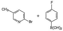 Compound B Approximately 250 mL of 1,2-dimethoxyethane and 100 mL of distilled water were added to a 1000 mL round bottom flask. To this mixture 15.0 g of 2-bromo-5-methyl pyridine, 12.2g of 4-fluorophenylboronic acid, 0.48 g of palladium (II) acetate, 2.3 g of triphenylphosphine and 23.0 g of sodium carbonate were added. This mixture was heated to reflux under nitrogen atmosphere for 16 hours. After the reaction was cooled, 150 mL. water and 150 mL ethyl acetate were added. The mixture was added to a separatory funnel and the organic and aqueous layers were allowed to separate. The organic layer was then washed with brine and dried over magnesium sulfate. After removal of the solvents by rotary evaporation, the crude mixture was purified by silica gel column chromatography using 10% EtOAc/hexanes as the eluent. The fractions containing the desired product were combined and the solvent was removed by rotary evaporation. About 100 mL of hexane was added to the obtained oil and cooled in ice water after which crystallization occurred. The crystals were isolated by vacuum filtration. Ten grams of white soHd was obtained. [00118] Compound E


To an oven dried 100 mL round bottom flask 10 mL of dry tefrahydrofuran and 0.54 g of diisopropylarnine were added. This mixture was cooled in an ice bath and 3.3 mL of 1.6 M n- butyl lithium was added drop wise. The mixture was stirred for 30 minutes and then 0.95 g of hexamethylphosphoramide were added drop wise. After stirring for 30 minutes, the reaction mixture was cooled to -78°C and then 1.0 g of compound B in 10 mL of dry tefrahydrofuran was added drop wise. After stirring for 4 hours at -78 °C, 1.85 g of compound C in 15 mL of dry tefrahydrofuran was added drop wise. After stirring for 1 hour the reaction was quenched with water and extracted with ethyl acetate. The organic layer was then washed with brine and dried over magnesium sulfate. Removal of the solvent by rotary evaporation resulted in a brown oil which was purified by silica get column chromatography using 30% EtOAc/hexanes as the eluent. The fractions containing the desired product were combined and the solvent removed to yield 0.3 grams of white sohd.
[00119] Dopant G
+ lrCI3 + AgOCOCF3 Compound E


To a 100 mL round flask, 15 mL 1,2-dichlorobenzene, 1 mL water, 0.1 g of compound E, 0.05 g of IrCl3, and 0.13 g of silver trifluoro acetate were added. This mixture was heated to reflux under nitrogen for 5 hours. After cooling to room temperature the reaction mixture was passed through a silica gel plug with 50% MeCl2/hexanes as the eluent. The desired fractions were combined and the solvent removed in vacuo. Yellow crystals were collected from a dichloromethane/methanol mixture. The desired product was confirmed by mass specfroscopy. Emission of the material in dichloromethane gave a λmax at 480 nm.
Example 3 - Synthesis of Dopant H [00120] Dopant H
+ RhCl3 + AgOCOCF3 Compound E


To a 100 mL round bottom flask 15 mL 1,2-dichlorobenzene, 1 mL water, 0.1 g of compound E, 0.04 g RhCl3 g of silver trifluoroacetate were added. This mixture was heated to reflux under nitrogen for 5 hours. After cooling to room temp the reaction mixture was passed through a silica gel plug with 50% CH2Cl2 hexanes as the eluent. The desired fractions were combined and the solvent removed in vacuo. White crystals were collected from a dichloromethane/methanol mixture. The desired product was confirmed by mass specfroscopy. Emission of the material in dichloromethane gave a λmax at 456 nm.
Example 4 - Device Comparison [00121] Device fabrication and measurement All devices are fabricated by high vacuum (<10"7 Torr) thermal evaporation. The anode electrode is -1200 A of indium tin oxide (ITO). The cathode consists of 10 A of LiF followed by 1,000 A of Al. All devices are encapsulated with a glass lid sealed with an epoxy resin in a nitrogen glove box (<1 ppm of H2O and O2) immediately after fabrication, and a moisture getter was incorporated inside the package. [00122] The current- voltage-luminance (LVL) characteristics and operational Hfetime are measured and summarized in the Table 1. A typical display brightness level of 600 cd/m2 for green emitting devices is chosen for the comparison between different devices. Table 1

Linked Ligand Device [00123] The organic stack consists of 100 A thick of copper phthalocyanine (CuPc) as the hole injection layer (HIL), 300 A of 4,4'-bis[N-(l-naphthyl)-N-phenylamino]biphenyl (α- NPD), as the hole fransporting layer (HTL), 300 A of 4,4'-bis(N-carbazolyl)biphenyl (CBP) doped with 4.5, 6 or 9 wt% of Dopant F as the emissive layer (EML). The ETL2 is 100 A of aluminum(III)bis(2-methyl-8-hydroxyqumolinato)4-phenylphenolate (BAlq). The ETL1 is 400 A of tris(8-hydroxyquinolinato)aluminum (Alq3). Comparative Example 1 [00124] The organic stack consists of 100 A thick of copper phthalocyanine (CuPc) as the hole injection layer (HIL), 300 A of 4,4'-bis[N-(l-naphthyl)-N-phenylamino]biphenyl ( - NPD), as the hole fransporting layer (HTL), 300 A of 4,4'-bis(N-carbazolyl)biphenyl (CBP) doped with 6 wt% of Oc-tris(2-phenylpyridine)iridium [Ir(ppy)3] as the emissive layer (EML). The ETL2 is 100 A of aluminum(III)bis(2-methyl-8-quinolinato)4-phenylphenolate (BAlq). The ETL1 is 400 A of tris(8-hydroxyquinol ato)aluπunum (Alq3). [00125] The linked ligand devices of Example 4 were characterized. The device characteristics are shown in Figures 3-6. The plot of current density vs voltage is shown in Figure 3. Figure 4 shows the plot of the external quantum efficiency at various current densities for these devices. Figure 5 shows the plots of luminous efficiency for these devices. The devices show high quantum efficiency and luminous efficiencies. The device having a dopant concentration of 4.5% gave a maximum quantum efficiency of 10% and a maximum luminous efficiency of 36 cd/A. Figure 6 shows the luminescent spectra for the device having dopant concentration of 4.5%, 6% and 9%. [00126] The operational stability of the 4.5% doped linked Hgand device was tested at room temperature under a constant direct current drive to achieve an initial luminance of 955 cd/m2. A comparison of stability was made to the comparative example 1 (unlinked ligand device) which was driven at a lower initial luminance of 600 cd/m2 (Figure 7). Without the enhanced stability provided by the present invention, one would have expected the device which was driven at higher initial luminance, to degrade more rapidly. The results indicate, however, that the Hnked ligands of the present invention exhibit enhanced stability since the linked Hgand device of Example 4 degraded less than the unlinked ligand device (comparative Example 1) when operating at a 37% higher brightness. As shown, the linked ligand device utilizing Dopant F retains 91% of 955 cd/m2 after 1000 hours of operation whereas comparative Example 1 utilizing unlinked Ir(ppy)3 retains only 89% of 600 cd/m2, after 1,000 hrs of continuous operation.
Example 5 - Synthesis of Dopant M [00127] Compound J
Compound J

Approximately 250 mL of 1,2-dimethoxyethane and 170 mL of a 2 M sodium carbonate solution were added to a 1000 mL round bottom flask. To this mixture, 39.0 g of 2- bromopyridine, 25.0 g of 4-bromophenylboronic acid, 0.70 g of palladium (II) acetate, and 3.26 g of friphenylphosphine were added. This mixture was heated to reflux under nitrogen atmosphere for 16 hours. After the reaction was cooled, 200 mL of water and 150 mL of ethyl acetate were added. The mixture was added to a separatory funnel and the organic and aqueous layers were allowed to separate. The organic layer was then washed with brine and dried over magnesium sulfate. After removal of the solvents by rotary evaporation, the crude mixture was purified by silica gel column chromatography using 10% EtOAc/Hexanes as the eluent. The fractions containing the desired product were combined and the solvent was removed by rotary evaporation. 22.0 g of white solid was obtained. [00128] Compound K

Cyclohexene, Pd on Carbon Compound K -

Compound L

Approximately 200 mL of ethylene glycol, 1.85 g of Ir(AcAc)3, and 2.5 g of compound L were added to a 500 mL round bottom flask. The reaction was heated to 160°C under N2 for 18 hours and then allowed to cool. Methanol was added arid the yellow solids were filtered. These solids were dissolved in dichloromethane and filtered through a silica gel plug. The fractions containing the desired product were combined and the solvent was removed by rotary evaporation. The yellow solids were recrystalHzed from dichlormethane/methanol and filtered to yield 1.5 g of the desired product, which was characterized by mass specfroscop}'' and NMR. The product was further purified by sublimation. Example 6 - Device Comparison [00131] Linked hexadentate molecules, Dopant M and Dopant F and the analogous unlinked tris ligand Ir(ppy)3 (Comparative Example 1) were compared as phosphorescent dopants in OLED devices. Devices were fabricated similarly to those in Example 4. The test device structure for each was ITO/CuPc(10θA)/NPD(30θA)/CBP: Dopant (4.5%, 30θA) /BAlq(lOθA) / Alq3(40θA) /LiF(loA)/Al(1000A) where the dopant was Dopant F, Dopant M, or the unlinked analog ligand Ir(ppy)3 (Comparative Example 1). A comparison of the device data for the three dopants is shown in Figures 8-10. The plot of current density vs voltage is shown in Figure 8. Figure 9 shows the plot of the external quantum efficiency as a function of current density for these devices. Figure 10 shows the electroluminescent spectra for these devices. These devices were found to have high external quantum efficiency with emission characteristic of the dopant. All of these dopants have nearly identical green emission at -510 nm. This demonstrates that the hexadentate linkage does not have a considerable effect on the color of emission. [00132] A comparison of the lifetime data can be seen in Figure 11. The devices were driven to 50% initial luminance at a constant direct current drive of 40mA/cm2 at room temperature. The Dopant M and Dopant F devices were found to have lifetimes of -300 hrs and -200 hrs, respectively, compared to a lifetime -130 hrs of the Ir(ppy)3 device. As in Example 4, the results indicate that the complexes with linked ligands of the present invention exhibit enhanced stability since the Dopant F and Dopant M devices both degraded less than the device doped with a complex with unlinked ligands of Comparative Example 1. [00133] Dopant M is a hexadentate iridium 2-phenylpyridine (ppy) complex analogous to Dopant F except that Dopant M is linked through the phenyl rings while Dopant F is linked through the pyridine rings. In general, it is beHeved that tethering the ligands of metal chelate complexes improves the stability with respect to Hgand dissociation degradation pathways. These pathways may occur both thermally (for example, during fabrication at temperatures compatible with OLED manufacturing processes) and electrochemically (for example, oxidation reduction during device operation). In this Example, a comparison of these two analogous hexadentate ligands indicates that linking through the phenyl rings may lower the rate of ligand dissociation even more effectively than Hnking through the pyridine rings. These observations may indicate a ligand dissociation pathway through Ir-C (phenyl ring) bond cleavage. Example 7 - Synthesis of Dopant Q
[00134] CompoundN
Compound K

Approximately 300 mL of 1,2-dimethoxyethane and 200 mL of water were added to a 1000 mL round bottom flask. To this mixture, 30.0 g of 2,5-dibromopyridine, 20.0 g of 2,4- difluorophenylboronic acid, 0.71 g of palladium (II) acetate, and 3.3 g of triphenylphosphine, and 36.3 g of sodium carbonate were added. This mixture was heated to reflux under nitrogen atmosphere for 16 hours. After the reaction was cooled, 200 mL water and 200 mL ethyl acetate were added. The mixture was added to a separatory funnel and the organic and aqueous layers were allowed to separate. The organic layer was then washed with brine and dried over magnesium sulfate. After removal of the solvents by rotary evaporation, the crude mixture was purified by silica gel column chromatography using 10% EtOAc Hexanes as the eluent. The fractions containing the desired product were combined and the solvent was removed by rotary evaporation. The product was crystaUized from dichloromethane and hexanes. 20 g of a white solid was obtained. [00135] Compound O

Approximately"100 mL of dry toluene, 100 mL dry diisopropylamine, 15.0 g of Compound N, and 1.9 g of tefrakis (friphenylphosphine) palladium were added to a 500 mL round bottom flask. This mixture was heated to 60°C for 30 minutes and then 2.8 grams of 1,3,5 triethynylbenzene and 0.21 grams of copper (I) iodide were added. The reaction was maintained at 60°C for 12 hours and then allowed to cool. The soHds were filtered and redispersed in refluxing dichloromethane. The slurry was filtered and dried to yield 12 g of a white solid. [00136] Compound P
Compound O

[00137] Approximately 100 mL cyclohexene, 100 mL tefrahydrofuran, 6.0 g of 10% Pd on Carbon, and 12 g of Compound O were added to a 250 mL round bottom flask. The reaction mixture was heated to reflux for 24 hours and then allowed to cool. The solids were removed by filfration and the solvent removed from the filtrate by rotary evaporation. The product was purified by silica gel column chromatography using 60% hexanes/ethyl acetate as the eluent. The fractions containing the desired product were combined and the solvent was removed by rotary evaporation. The pure product was crystallized from ethyl acetate / hexanes and filtered to yield 8.0 g of a white solid. [00138] Dopant Q
Compound P

Approximately 250 mL of ethylene glycol, 1.55 g of Ir(AcAc)3, and 2.3 grams of compound P were added to a 500 mL round bottom flask. The reaction was heated to reflux under N2 for 18 hours and then allowed to cool. Methanol was added and the yellow solids were filtered. The solids were dissolved in refluxing 1,2-dichlorobenzene and allowed to cool. The solids were filtered to yield 1.5 g of yellow product, which was confirmed by mass specfroscopy and NMR. The product was further purified by sublimation.
Example 8 - Device Comparison
[00139] Linked Ligand Device. In the Dopant Q device, the organic stack consisted of 100 A thick of copper phthalocyanine (CuPc) as the hole mjecύon layer (HIL), 300 A of 4,4 ' - bis[N-(l-naphthyl)-N-phenylamino]biphenyl (α-NPD), as the hole fransporting layer (HTL), 300 A of N,N'-dicarbazolyl-3,5-benzene (mCP) doped with 6 wt% of Dopant Q as the emissive layer (EML). The ETL2 is 400 A of alummum(πi)bis(2-methyl-8-quinolinato)4- phenylphenolate (BAlq). There was no ETL1. Comparative example 2 [00140] In the unlinked comparative example, the organic stack consisted of 100 A thick of copper ph alocyanine (CuPc) as the hole injection layer (HIL), 300 A of 4,4'-bis[N-(l - naphthyl)-N-phenylamino]biphenyl ( -NPD), as the hole fransporting layer (HTL), 300 A of N,N'-dicarbazolyl-3,5-benzene (mCP) doped with 6 wt% of Ir(4,6-F2ppy)3 as the emissive layer (EML). The ETL2 is 400 A of aluminum(m)bis(2-methyl-8-quinolinato)4- phenylphenolate (BAlq). There was no ETL1. [00141] Devices were fabricated similarly to those in Example 4. The current- voltage plot, external quantum efficiency vs current density, elecfroluminescence spectra, and room temperature operational stability (constant current of 5 mA/cm2) in terms of normalized elecfroluminescence vs time of the Dopant Q device and Comparative Example 2 [Ir(4,6- F ppy)3] are shown in Figure 12, Figure 13, Figure 14 and Figurel5 respectively. The efficiency of the devices containing the ligand-linked complex (Dopant Q) is lower than that of the unlinked analog Comparative Example 2 [Ir(4,6-F2ppy)3]. However, the operational stability the devices containing the Hgand-linked complex (Dopant Q) is similar to that of the unlinked analog Comparative Example 2 [Ir(4,6-F2ppy)3]. In this case, there is very little or no improvement in lifetime between devices containing the linked and unlinked complexes. However, as shown in Examples 4 and 6, devices containing the Hnked versions of the Ir(ppy)3 type complex clearly exhibit enhanced stability compared to the unlinked Ir(ppy)3. The lack of improvement in the Ir(4,6-F2ρpy)3 type complex may be due to the electrochemical instability of fluorine substituents, which perhaps results in ligand degradation due to the reductive elimination of fluorine upon device operation. The enhanced chelating effect of the ligand to the metal center which is believed to improve the stability of the complex may not have a significant effect in such a degradation mechanism. A further possibility is that the degradation mechanism occurs primarily through the cleavage of the Ir-C bond. As shown in Example 6, Dopant M, where the Hgands are linked through the phenyl ring, are more stable than devices using dopant F, with ligands Hnked through the pyridine ring. If this is the case, linking the ligands through the pyridine rings may not show a significant improvement in stability for high energy dopants substituted with fluorine, such as Dopant Q. [00142]' While the present invention is described with respect to particular examples and preferred embodiments, it is understood that the present invention is not limited to these examples and embodiments. The present invention as claimed therefore includes variations from the particular examples and preferred embodiments described herein, as will be apparent to one of skill in the art.
Claims
1. An organic Hght emitting device comprising an anode, a cathode, and an organic layer disposed between the anode and the cathode, wherein the organic layer comprises a phosphorescent organometaUic emissive material comprising a transition metal, and two or three bidentate ligands, wherein two or more of the bidentate Hgands are covalentiy linked by a linking group, wherein, the bidentate ligands are selected from bidentate photoactive ligands, wherein each bidentate photoactive ligand is bound to the transition metal through a carbon-metal bond and a nitrogen-metal bond to form a cyclometallated ring, and bidentate ancHlary ligands, wherein at least one of the bidentate Hgands is a bidentate photoactive Hgand.
2. The organic light entitling device of claim 1 ,■ wherein the linking group provides no %- conjugation between the linked bidentate Hgands.
3. An organic Hght emitting device comprising an anode, a cathode, and an organic layer disposed between the anode and the cathode, wherein the organic layer comprises an emissive material having the formula I wherein, M is a transition metal having a molecular weight greater than 40; X is a linking group that links two or more L, and is selected from the group consisting of -(CR2)d-, -[O(CR2)e]O-, or a group having the formula A A-Bx-A or A-B^-A wherein A is -(CRa) -, or -Z-(CR2) ; Z is -0-, -NR-, or -SiR2-;

33 B1 is -O-, -NR-, -CR=CR-, aryl, heteroaryl, cycloalkyl, or aheterocycHc group,? i I B is -N- , — CR— , alkyl, aryl, heteroaryl, cycloalkyl, or a heterocyclic group; each R is independently selected from H, alkyl, aralkyl, aryl and heteroaryl, d is 1 to 6, e is 1 to 6, fis 1 to 4, and g is 1 to 4;
L is a bidentate ligand selected from the group consisting of (i) bidentate photoactive ligands having the formula II R4
R2^^C (ID wherein the bidentate photoactive ligand is bound to the transition metal through a carbon- metal bond and a nitrogen-metal bond to form a cyclometallated ring, Y is N or C, the dotted line represents an optional double bond, R1, R2, R3 and R4 are independently selected from H, alkyl, or aryl, and additionally or alternatively, one or more of R1 and R2, R2 and R3, and R3 and R4 together from independently a 5 or 6-member cyclic group, wherein said cyclic group is cycloalkyl, cyclohetero alkyl, aryl or heteroaryl; and wherein said cyclic group is optionally substituted by one or more substituents Z; each substituent Z is independently selected from the group consisting of alkyl, alkenyl, alkynyl, aralkyl, CN, CF3, NR23 NO2, OR, halo, and aryl, and additionally, or alternatively, two Z groups on adjacent ring atoms form a fused 5- or 6-membered aromatic group, and each R is independently selected from H, alkyl, aralkyl, aryl and heteroaryl; and (ii) bidentate ancillary ligands, a is 1 to 4; b is 2 or 3; and at least one L is selected from a bidentate photoactive Hgand.
4. The organic light ermtting device of claim 3, wherein the photoactive ligands are selected from compounds of the formula LV

5. The organic Hght emitting device of claim 3, wherein [Xa-(L)j] has the formula:


6. The organic Hght emitting device of claim 3 , wherein the emissive material is a compound having the formula

7. The organic light emitting device of claim 3, wherein the emissive material is a compound having the formula

8. The organic light emitting device of claim 3, wherein the emissive material is a compound having the formula

9. A compound of the formula I [Xfl-(L)6]M (I) wherein, M is a fransition metal having a molecular weight greater than 40; X is a linking group that links two or more L, and is selected from the group consisting of -(CR2)<r, -[O(CR2)JO-, or a group having the formula A A-B^A or A-B^-A wherein A is -(CR2) -, or -Z-(CR2) ; Z is -O-, -NR-, or -SiR2-; B1 is -0-, -NR-, -CR=CR-, aryl, heteroaryl, cycloalkyl, or a heterocycli-c group, B 2 is — N I — , — C ' R— , alkyl, aryl, heteroaryl, cycloalkyl, or a heterocyclic group; each R is independently selected from H, alkyl, aralkyl, aryl and heteroaryl, d is 1 to 6, e is 1 to 6, /is 1 to 4, and g is 1 to 4; L is a bidentate Hgand selected from the group consisting of (i) bidentate photoactive ligands having the formula II R4
R2/ ^C R1 (n) wherein the bidentate photoactive Hgand is bound to the fransition metal through a carbon- metal bond and a nitrogen-metal bond to form a cyclometallated ring, Y is N or C, the dotted line represents an optional double bond, R1, R2, R3 and R4 are independently selected from H, alkyl, or aryl, and additionally or alternatively, one or more of R1 and R2, R2 and R3, and R3 and R4 together from independently a 5 or 6-member cyclic group, wherein said cyclic group is cycloalkyl, cycloheteroalkyl, aryl or heteroaryl; and wherein said cyclic group is optionaHy substituted by one or more substituents Z; each substituent Z is independently selected from the group consisting of alkyl, alkenyl, alkynyl, aralkyl, CN, CF3, NR2, NO2, OR, halo, and aryl, and additionally, or alternatively, two Z groups on adjacent ring atoms form a fused 5- or 6-membered aromatic group, and (ii) bidentate ancillary ligands, each R is independently selected from H, alkyl, aralkyl, aryl and heteroaryl; a is 1 to 4; b is 2 or 3; and at least one L is selected from a bidentate photoactive ligand.
10. The compound of claim 9, wherein the photoactive ligands are selected from compounds of the formula LV

11. The compound of claim 9, wherein [Xα-(L)έ] has the formula:

12. The compound of claim 9, having the formula

13. The compound of claim 9, having the formula

14. The compound of claim 9, having the formula

15. An organic Hght emitting device comprising an anode, a cathode, and an organic layer disposed between the anode and the cathode, wherein the organic layer comprises a material of the formula VLI A1[Q/,(XH-] (VII) wherein Q is a bidentate ligand of the formula VLII


16. The organic light emitting device of claim 15, wherein the linking group provides no π- conjugation between the linked bidentate ligands.
17. The organic light emitting device of claim 15, wherein the linking group X is selected from the group consisting of -(CR2 , -[O(CR2)JO-, or a group having the formula A A-BJ-A or A-B2-A wherein A is -(CR2V-, or -Z-(CR2) ; Z is -O-, -NR-, or -SiR2-; B1 is -O-, -NR-, -CR=CR-, aryl, heteroaryl, cycloalkyl, or a heterocyclic group, B 2 is — ' — , — C ' R— , alkyl, aryl, heteroaryl, cycloalkyl, or a heterocyclic group; each R is independently selected from H, alkyl, aralkyl, aryl and heteroaryl, d is 1 to 6, e is 1 to 6, fis 1 to 4, and g is 1 to 4.
18. The organic Hght emitting device of claim 15, wherein the bidentate ligand Q has the formula

19. The organic Hght emitting device of claim 15, wherein/ is 0 and h is 3.
20. The organic Hght emitting device of claim 15, wherein j is 1 and h is 2.
21. The organic light emitting device of claim 15, wherein [QΛ ] has the formula

22. The organic Hght emitting device of claim 15, wherein the organic layer comprises a material of the formula

23. A compound of the formula VII Al[Q»(X)|J] (VH) wherein
Q is a bidentate ligand of the formula VIII


24. The compound of claim 23, wherein the linking group provides no π-conjugation between the linked bidentate ligands.
25. The compound of claim 23, wherein the linking group X is selected from the group consisting of -(CR2)i-, -[O(CR2)JO-, or a group having the formula A A-B3-A or A-B2-A wherein A is -(CR2)r, or -Z-(CR2V; Z is -O-, -NR-, or -SiR2-; B1 is -O-, -NR-, -CR=CR-, aryl, heteroaryl, cycloalkyl, or a heterocyclic group, B ? is — N ' — , — C I R— , alkyl, aryl, heteroaryl, cycloalkyl, or a heterocyclic group; each R is independently selected from H, alkyl, aralkyl, aryl and heteroaryl, d is 1 to 6, e is 1 to 6, /is 1 to 4, and g is 1 to 4.
26. The compound of claim 23, wherein the bidentate ligand Q has the formula

27. The compound of claim 23, whereiny is 0 and h is 3.
28. The compound of claim 23, whereiny is 1 and h is 2.
29. The compound of claim 23, wherein [QA(X)ZJ,-] has the formula


30. The compound of claim 23, having the formula

31. An organic light emitting device comprising an anode, a cathode, and an organic layer disposed between the anode and the cathode, wherein the organic layer comprises a metal complex comprising: a metal; a first Hgand bound to the metal, wherein the first Hgand is a bidentate Hgand; a second Hgand bound to the metal; and a linking group that covalentiy links the first Hgand and the second ligand, wherein the linking group provides no π-conjugation between the first ligand and the second Hgand.
32. The organic light enntting device of claim 31, wherein the metal complex is a phosphorescent organometallic emissive material.
33. The organic light emitting device of claim 31, wherein the metal complex further comprises an additional bidentate ligand.
34. The organic light emitting device of claim 31, wherein the second ligand is a bidentate ligand.
35. The organic Hght emitting device of claim 31, wherein the second ligand is a monodentate ligand.
36. The organic Hght emitting device of claim 31, wherein the metal is duminum.
37. The organic light ernitting device of claim 3, wherein [Xα-(L)j] has the formula:


38. The organic light emitting device of claim 3 , wherein [Xfl-(L)&] has the formula:

39. The organic light enntting device of claim 3, wherein [Xa-(L)b] has the formula:

40. The organic light einitting device of claim 3, wherein the emissive material is a compound having the formula

41. The compound of claim 9, wherein [Xα-(L)&] has the formula:


42. The compound of claim 9, wherein [Xfl-(L)J has the formula:

43. The compound claim 9, wherein [Xα-(L)i] has the formula:

44. The compound of claim 9, having the formula:

45. The organic Hght enutting device of claim 3, wherein the emissive material is a compound having the formula:

46. The compound of claim 9 having the formula:

47. The.organic light emitting device of claim 3, wherein two or more L comprise a phenyl moiety and X is a linking group that links the two or more L via a covalent bond to the phenyl moiety in each of the two or more L.
48. The organic light emitting device of claim 3, wherein Xa-(L)b] has the formula


49. The organic light emitting device of claim 48, wherein [Xa-(L)b] has the formula:

50. The organic light emitting device of claim 48, wherein fXβ-(L),&] has the formula:

51. The compound of claim 9, wherein X is linked to each L via a covalent bond to a pyridyl moiety in each L.
52. The compound of claim 9, wherein [Xα-(L)J has the formula:

53. The compound of claim 52, wherein [Xα-(L)J has the formula:

54. The compound of claim 52, wherein [Xα-(L)&] has the formula:

55. An organic light emitting device comprising an anode, a cathode, and an organic layer disposed between the anode and the cathode, wherein the organic layer comprises a phosphorescent organometallic emissive material comprising a metal bound to two or three bidentate ligands, wherein two or more of the bidentate ligands are covalentiy linked by one or more linking groups.
56. The organic light emitting device of claim 55 wherein the organometallic emissive material comprises a compound represented by the formula [Xa-(L)b]M wherein M is a transition metal, L is a bidentate ligand, X is a linking group that links two or more L, a is 1 to 4, b is 2 or 3 wherein the bidentate Hgands are selected from bidentate photoactive Hgands, and bidentate ancillary ligands wherein at least one of the bidentate ligands is a bidentate photoactive Hgand.
57. A compound of the formula [Xa-(L)b]M wherein M is a fransition metal, L is a bidentate ligand, X is a linking group that links two or more L, a is 1 to 4, b is 2 or 3 wherein the bidentate Hgands are selected from bidentate photoactive ligands, and bidentate ancillary ligands wherein at least one of the bidentate ligands is a bidentate photoactive ligand bound to the transition metal through a carbon-metal bond.
58. The organic Hght entitling device of claim 1 wherein the transition metal is selected from the group consisting of Ir, Pt, Pd, Rh, Re, Os, Tl, Pb, Bi, In, Sn, Sb, Te, Au, and Ag.
59. The organic light entitling device of claim 1 wherein the transition metal is Ir.
60. The organic light emitting device of claim 3 wherein the transition metal is selected from the group consisting of Ir, Pt, Pd, Rh, Re, Os, Tl, Pb, Bi, Hi, Sn, Sb, Te, Au, and Ag.
61. The organic light emitting device of claim 3 wherein the fransition metal is Ir.
62. The compound of claim 9 wherein the fransition metal is selected from the group consisting of Ir, Pt, Pd, Rh, Re, Os, Tl, Pb, Bi, In, Sn, Sb, Te, Au, and Ag.
63. The compound of claim 9 wherein the transition metal is Ir.
64. The organic light emitting device of claim 56 wherein the fransition metal is selected from the group consisting of Ir, Pt, Pd, Rh, Re, Os, Tl, Pb, Bi, In, Sn, Sb, Te, Au, and Ag.
65. The organic light enfrtting device of claim 56 wherein the transition metal is Ir.
66. The compound of claim 57 wherein the transition metal is selected from the group consisting of Ir, Pt, Pd, Rh, Re, Os, Tl, Pb, Bi, In, Sn, Sb, Te, Au, and Ag.
67. The compound of claim 57 wherein the fransition metal is Ir.
Applications Claiming Priority (4)
| Application Number | Priority Date | Filing Date | Title |
|---|---|---|---|
| US10/771,423 | 2004-02-03 | ||
| US10/771,423US20050170206A1 (en) | 2004-02-03 | 2004-02-03 | OLEDs utilizing multidentate ligand systems |
| US10/859,796US7332232B2 (en) | 2004-02-03 | 2004-06-03 | OLEDs utilizing multidentate ligand systems |
| US10/859,796 | 2004-06-03 |
Publications (2)
| Publication Number | Publication Date |
|---|---|
| WO2005076380A2true WO2005076380A2 (en) | 2005-08-18 |
| WO2005076380A3 WO2005076380A3 (en) | 2005-11-03 |
Family
ID=34841274
Family Applications (1)
| Application Number | Title | Priority Date | Filing Date |
|---|---|---|---|
| PCT/US2005/003107WO2005076380A2 (en) | 2004-02-03 | 2005-01-26 | Oleds utilizing multidentate ligand systems |
Country Status (3)
| Country | Link |
|---|---|
| US (1) | US7332232B2 (en) |
| TW (1) | TWI365219B (en) |
| WO (1) | WO2005076380A2 (en) |
Cited By (28)
| Publication number | Priority date | Publication date | Assignee | Title |
|---|---|---|---|---|
| WO2007018067A1 (en)* | 2005-08-05 | 2007-02-15 | Idemitsu Kosan Co., Ltd. | Transition metal complex compound and organic electroluminescent device using same |
| WO2007086505A1 (en)* | 2006-01-27 | 2007-08-02 | Idemitsu Kosan Co., Ltd. | Transition metal complex compound and organic electroluminescent device using same |
| JP2013033915A (en)* | 2011-07-06 | 2013-02-14 | Konica Minolta Holdings Inc | Organic electroluminescent element, display device, and lighting device |
| WO2013038804A1 (en) | 2011-09-12 | 2013-03-21 | 新日鉄住金化学株式会社 | Organic electroluminescent element |
| WO2013038843A1 (en) | 2011-09-12 | 2013-03-21 | 新日鉄住金化学株式会社 | Organic electroluminescent element |
| WO2013038929A1 (en) | 2011-09-12 | 2013-03-21 | 新日鉄住金化学株式会社 | Organic electroluminescent element material having silicon-containing four membered ring structure, and organic electroluminescent element |
| WO2013088934A1 (en) | 2011-12-12 | 2013-06-20 | 新日鉄住金化学株式会社 | Organic electroluminescent element material and organic electroluminescent element using same |
| JP2013145811A (en)* | 2012-01-13 | 2013-07-25 | Konica Minolta Inc | Organic electroluminescent element, display device, and lighting device |
| EP2623508A1 (en) | 2012-02-02 | 2013-08-07 | Konica Minolta Advanced Layers, Inc. | Iridium complex compound, organic electroluminescent element material, organic electroluminescent element, illumination device and display device |
| WO2013137001A1 (en) | 2012-03-12 | 2013-09-19 | 新日鉄住金化学株式会社 | Organic electroluminescent element |
| WO2014002629A1 (en) | 2012-06-28 | 2014-01-03 | 新日鉄住金化学株式会社 | Organic electroluminescence element and material for organic electroluminescence element |
| WO2014013936A1 (en) | 2012-07-19 | 2014-01-23 | 新日鉄住金化学株式会社 | Organic electroluminescent element |
| WO2014030666A1 (en) | 2012-08-24 | 2014-02-27 | コニカミノルタ株式会社 | Transparent electrode, electronic device, and method for manufacturing transparent electrode |
| WO2014050904A1 (en) | 2012-09-28 | 2014-04-03 | 新日鉄住金化学株式会社 | Compound for organic electroluminescent elements, and organic electroluminescent element |
| WO2014097813A1 (en) | 2012-12-17 | 2014-06-26 | 新日鉄住金化学株式会社 | Organic electrical field light-emitting element |
| WO2014157618A1 (en) | 2013-03-29 | 2014-10-02 | コニカミノルタ株式会社 | Organic electroluminescent element, and lighting device and display device which are provided with same |
| US9673405B2 (en) | 2011-03-01 | 2017-06-06 | Konica Minolta Holdings, Inc. | Organic electroluminescent device, display apparatus, and lighting apparatus |
| EP3200255A2 (en) | 2016-01-06 | 2017-08-02 | Konica Minolta, Inc. | Organic electroluminescent element, method for producing organic electroluminescent element, display, and lighting device |
| CN107207550A (en)* | 2015-02-03 | 2017-09-26 | 默克专利有限公司 | metal complex |
| CN107814821A (en)* | 2012-01-12 | 2018-03-20 | Udc 爱尔兰有限责任公司 | Metal complex with dibenzo [F, H] quinoxaline |
| CN107922451A (en)* | 2015-08-25 | 2018-04-17 | 默克专利有限公司 | Metal complex |
| JP2019052137A (en)* | 2017-08-10 | 2019-04-04 | ユニバーサル ディスプレイ コーポレイション | Organic electroluminescent materials and devices |
| KR20190047089A (en)* | 2016-09-21 | 2019-05-07 | 메르크 파텐트 게엠베하 | A bimetallic metal complex for use as an emitter in an organic electroluminescent device |
| WO2019181465A1 (en) | 2018-03-19 | 2019-09-26 | 日鉄ケミカル&マテリアル株式会社 | Organic electroluminescence element |
| JP2019527684A (en)* | 2016-07-14 | 2019-10-03 | メルク、パテント、ゲゼルシャフト、ミット、ベシュレンクテル、ハフツングMerck Patent GmbH | Metal complex |
| JP2019534244A (en)* | 2016-08-30 | 2019-11-28 | メルク、パテント、ゲゼルシャフト、ミット、ベシュレンクテル、ハフツングMerck Patent GmbH | Metal complex |
| CN111836820A (en)* | 2018-03-19 | 2020-10-27 | 默克专利有限公司 | metal complex |
| EP4271160A2 (en) | 2015-02-13 | 2023-11-01 | Merck Patent GmbH | Aromatic heterocyclic derivative, and organic electroluminescent element, illumination device, and display device using aromatic heterocyclic derivative |
Families Citing this family (652)
| Publication number | Priority date | Publication date | Assignee | Title |
|---|---|---|---|---|
| DE10310887A1 (en)* | 2003-03-11 | 2004-09-30 | Covion Organic Semiconductors Gmbh | Matallkomplexe |
| US7569692B2 (en) | 2003-06-02 | 2009-08-04 | Fujifilm Corporation | Organic electroluminescent devices and metal complex compounds |
| DE10350722A1 (en)* | 2003-10-30 | 2005-05-25 | Covion Organic Semiconductors Gmbh | metal complexes |
| US7709100B2 (en)* | 2004-07-07 | 2010-05-04 | Universal Display Corporation | Electroluminescent efficiency |
| US9070884B2 (en) | 2005-04-13 | 2015-06-30 | Universal Display Corporation | Hybrid OLED having phosphorescent and fluorescent emitters |
| TWI418606B (en)* | 2005-04-25 | 2013-12-11 | Udc Ireland Ltd | Organic electroluminescent device |
| TWI391027B (en)* | 2005-04-25 | 2013-03-21 | Fujifilm Corp | Organic electroluminescent device |
| US8586204B2 (en) | 2007-12-28 | 2013-11-19 | Universal Display Corporation | Phosphorescent emitters and host materials with improved stability |
| US9051344B2 (en) | 2005-05-06 | 2015-06-09 | Universal Display Corporation | Stability OLED materials and devices |
| US7851072B2 (en)* | 2005-05-19 | 2010-12-14 | Universal Display Corporation | Stable and efficient electroluminescent materials |
| GB0518968D0 (en) | 2005-09-16 | 2005-10-26 | Cdt Oxford Ltd | Organic light-emitting device |
| US7759489B2 (en) | 2006-01-27 | 2010-07-20 | Idemitsu Kosan Co., Ltd. | Transition metal complex compound and organic electroluminescence device using the compound |
| KR20180117719A (en) | 2006-02-10 | 2018-10-29 | 유니버셜 디스플레이 코포레이션 | METAL COMPLEXES OF CYCLOMETALLATED IMIDAZO[1,2-f]PHENANTHRIDINE AND DIIMIDAZO[1,2-A:1',2'-C]QUINAZOLINE LIGANDS AND ISOELECTRONIC AND BENZANNULATED ANALOGS THEREOF |
| CN103087109B (en) | 2007-03-08 | 2015-10-28 | 通用显示公司 | Phosphor material |
| US9130177B2 (en) | 2011-01-13 | 2015-09-08 | Universal Display Corporation | 5-substituted 2 phenylquinoline complexes materials for light emitting diode |
| US20130032785A1 (en) | 2011-08-01 | 2013-02-07 | Universal Display Corporation | Materials for organic light emitting diode |
| EP2511254B1 (en) | 2007-08-08 | 2016-05-11 | Universal Display Corporation | Single triphenylene chromophores in phosphorescent light emitting diodes |
| EP3159333B1 (en) | 2007-08-08 | 2020-04-22 | Universal Display Corporation | Benzo-fused thiophene or furan compounds comprising a triphenylene group |
| US8476822B2 (en)* | 2007-11-09 | 2013-07-02 | Universal Display Corporation | Saturated color organic light emitting devices |
| WO2009073245A1 (en) | 2007-12-06 | 2009-06-11 | Universal Display Corporation | Light-emitting organometallic complexes |
| WO2009085344A2 (en) | 2007-12-28 | 2009-07-09 | Universal Display Corporation | Dibenzothiophene-containing materials in phosphorescent light emitting diodes |
| DE102008015526B4 (en)* | 2008-03-25 | 2021-11-11 | Merck Patent Gmbh | Metal complexes |
| KR101778910B1 (en) | 2008-06-30 | 2017-09-14 | 유니버셜 디스플레이 코포레이션 | Hole transport materials containing triphenylene |
| WO2010027583A1 (en) | 2008-09-03 | 2010-03-11 | Universal Display Corporation | Phosphorescent materials |
| TWI482756B (en) | 2008-09-16 | 2015-05-01 | Universal Display Corp | Phosphorescent substance |
| CN103094490B (en) | 2008-09-25 | 2016-03-09 | 通用显示公司 | Organic Selenium material and the purposes in organic light emitting apparatus thereof |
| CN103396455B (en)* | 2008-11-11 | 2017-03-01 | 通用显示公司 | Phosphorescent emitters |
| US8815415B2 (en) | 2008-12-12 | 2014-08-26 | Universal Display Corporation | Blue emitter with high efficiency based on imidazo[1,2-f] phenanthridine iridium complexes |
| US9067947B2 (en) | 2009-01-16 | 2015-06-30 | Universal Display Corporation | Organic electroluminescent materials and devices |
| US11910700B2 (en) | 2009-03-23 | 2024-02-20 | Universal Display Corporation | Heteroleptic iridium complexes as dopants |
| US8722205B2 (en) | 2009-03-23 | 2014-05-13 | Universal Display Corporation | Heteroleptic iridium complex |
| US8709615B2 (en) | 2011-07-28 | 2014-04-29 | Universal Display Corporation | Heteroleptic iridium complexes as dopants |
| TWI730274B (en) | 2009-04-28 | 2021-06-11 | 美商環球展覽公司 | Iridium complex with methyl-d3 substitution |
| US8586203B2 (en) | 2009-05-20 | 2013-11-19 | Universal Display Corporation | Metal complexes with boron-nitrogen heterocycle containing ligands |
| US8545996B2 (en) | 2009-11-02 | 2013-10-01 | The University Of Southern California | Ion-pairing soft salts based on organometallic complexes and their applications in organic light emitting diodes |
| US8580394B2 (en) | 2009-11-19 | 2013-11-12 | Universal Display Corporation | 3-coordinate copper(I)-carbene complexes |
| US8288187B2 (en) | 2010-01-20 | 2012-10-16 | Universal Display Corporation | Electroluminescent devices for lighting applications |
| US9156870B2 (en)* | 2010-02-25 | 2015-10-13 | Universal Display Corporation | Phosphorescent emitters |
| US9175211B2 (en)* | 2010-03-03 | 2015-11-03 | Universal Display Corporation | Phosphorescent materials |
| WO2011119162A1 (en) | 2010-03-25 | 2011-09-29 | Universal Display Corporation | Solution processable doped triarylamine hole injection materials |
| US8968887B2 (en) | 2010-04-28 | 2015-03-03 | Universal Display Corporation | Triphenylene-benzofuran/benzothiophene/benzoselenophene compounds with substituents joining to form fused rings |
| JP5646733B2 (en) | 2010-04-28 | 2014-12-24 | ユニバーサル ディスプレイ コーポレイション | Premixed material deposition |
| KR20130067276A (en) | 2010-04-30 | 2013-06-21 | 아리조나 보드 오브 리젠츠 퍼 앤 온 비하프 오브 아리조나 스테이트 유니버시티 | Synthesis of four coordinated palladium complexes and their applications in light emitting devices thereof |
| US8673458B2 (en) | 2010-06-11 | 2014-03-18 | Universal Display Corporation | Delayed fluorescence OLED |
| US8742657B2 (en) | 2010-06-11 | 2014-06-03 | Universal Display Corporation | Triplet-Triplet annihilation up conversion (TTA-UC) for display and lighting applications |
| WO2012016074A1 (en) | 2010-07-29 | 2012-02-02 | University Of Southern California | Co-deposition methods for the fabrication of organic optoelectronic devices |
| JP5770289B2 (en) | 2010-08-20 | 2015-08-26 | ユニバーサル ディスプレイ コーポレイション | Bicarbazole compounds for OLED |
| US8932734B2 (en) | 2010-10-08 | 2015-01-13 | Universal Display Corporation | Organic electroluminescent materials and devices |
| US8269317B2 (en) | 2010-11-11 | 2012-09-18 | Universal Display Corporation | Phosphorescent materials |
| US20120138906A1 (en) | 2010-12-07 | 2012-06-07 | The University of Southern California USC Stevens Institute for Innovation | Capture agents for unsaturated metal complexes |
| US10008677B2 (en) | 2011-01-13 | 2018-06-26 | Universal Display Corporation | Materials for organic light emitting diode |
| US8415031B2 (en) | 2011-01-24 | 2013-04-09 | Universal Display Corporation | Electron transporting compounds |
| TWI541247B (en) | 2011-02-18 | 2016-07-11 | 美國亞利桑那州立大學董事會 | Four-coordinate platinum and palladium complex with geometrically distortion charge transfer state and its application in illuminating devices |
| US8748011B2 (en) | 2011-02-23 | 2014-06-10 | Universal Display Corporation | Ruthenium carbene complexes for OLED material |
| WO2012116231A2 (en) | 2011-02-23 | 2012-08-30 | Universal Display Corporation | Novel tetradentate platinum complexes |
| US9005772B2 (en) | 2011-02-23 | 2015-04-14 | Universal Display Corporation | Thioazole and oxazole carbene metal complexes as phosphorescent OLED materials |
| US8563737B2 (en) | 2011-02-23 | 2013-10-22 | Universal Display Corporation | Methods of making bis-tridentate carbene complexes of ruthenium and osmium |
| US8492006B2 (en) | 2011-02-24 | 2013-07-23 | Universal Display Corporation | Germanium-containing red emitter materials for organic light emitting diode |
| US8883322B2 (en) | 2011-03-08 | 2014-11-11 | Universal Display Corporation | Pyridyl carbene phosphorescent emitters |
| US8580399B2 (en) | 2011-04-08 | 2013-11-12 | Universal Display Corporation | Substituted oligoazacarbazoles for light emitting diodes |
| US8432095B2 (en) | 2011-05-11 | 2013-04-30 | Universal Display Corporation | Process for fabricating metal bus lines for OLED lighting panels |
| US8927308B2 (en) | 2011-05-12 | 2015-01-06 | Universal Display Corporation | Method of forming bus line designs for large-area OLED lighting |
| US8564192B2 (en) | 2011-05-11 | 2013-10-22 | Universal Display Corporation | Process for fabricating OLED lighting panels |
| US9212197B2 (en) | 2011-05-19 | 2015-12-15 | Universal Display Corporation | Phosphorescent heteroleptic phenylbenzimidazole dopants |
| US8795850B2 (en) | 2011-05-19 | 2014-08-05 | Universal Display Corporation | Phosphorescent heteroleptic phenylbenzimidazole dopants and new synthetic methodology |
| US8748012B2 (en) | 2011-05-25 | 2014-06-10 | Universal Display Corporation | Host materials for OLED |
| US9238668B2 (en) | 2011-05-26 | 2016-01-19 | Arizona Board Of Regents, Acting For And On Behalf Of Arizona State University | Synthesis of platinum and palladium complexes as narrow-band phosphorescent emitters for full color displays |
| US10158089B2 (en) | 2011-05-27 | 2018-12-18 | Universal Display Corporation | Organic electroluminescent materials and devices |
| US10079349B2 (en) | 2011-05-27 | 2018-09-18 | Universal Display Corporation | Organic electroluminescent materials and devices |
| KR20140041551A (en) | 2011-06-08 | 2014-04-04 | 유니버셜 디스플레이 코포레이션 | Heteroleptic iridium carbene complexes and light emitting device using them |
| US8884316B2 (en) | 2011-06-17 | 2014-11-11 | Universal Display Corporation | Non-common capping layer on an organic device |
| US8659036B2 (en) | 2011-06-17 | 2014-02-25 | Universal Display Corporation | Fine tuning of emission spectra by combination of multiple emitter spectra |
| US9252377B2 (en) | 2011-07-14 | 2016-02-02 | Universal Display Corporation | Inorganic hosts in OLEDs |
| US9397310B2 (en) | 2011-07-14 | 2016-07-19 | Universal Display Corporation | Organice electroluminescent materials and devices |
| US9023420B2 (en) | 2011-07-14 | 2015-05-05 | Universal Display Corporation | Composite organic/inorganic layer for organic light-emitting devices |
| US9783564B2 (en) | 2011-07-25 | 2017-10-10 | Universal Display Corporation | Organic electroluminescent materials and devices |
| US8409729B2 (en) | 2011-07-28 | 2013-04-02 | Universal Display Corporation | Host materials for phosphorescent OLEDs |
| US8926119B2 (en) | 2011-08-04 | 2015-01-06 | Universal Display Corporation | Extendable light source with variable light emitting area |
| US8552420B2 (en) | 2011-08-09 | 2013-10-08 | Universal Display Corporation | OLED light panel with controlled brightness variation |
| US9493698B2 (en) | 2011-08-31 | 2016-11-15 | Universal Display Corporation | Organic electroluminescent materials and devices |
| US8652656B2 (en) | 2011-11-14 | 2014-02-18 | Universal Display Corporation | Triphenylene silane hosts |
| US9193745B2 (en) | 2011-11-15 | 2015-11-24 | Universal Display Corporation | Heteroleptic iridium complex |
| US9217004B2 (en) | 2011-11-21 | 2015-12-22 | Universal Display Corporation | Organic light emitting materials |
| US9512355B2 (en) | 2011-12-09 | 2016-12-06 | Universal Display Corporation | Organic light emitting materials |
| US20130146875A1 (en) | 2011-12-13 | 2013-06-13 | Universal Display Corporation | Split electrode for organic devices |
| US9461254B2 (en) | 2012-01-03 | 2016-10-04 | Universal Display Corporation | Organic electroluminescent materials and devices |
| US8987451B2 (en) | 2012-01-03 | 2015-03-24 | Universal Display Corporation | Synthesis of cyclometallated platinum(II) complexes |
| US9163174B2 (en) | 2012-01-04 | 2015-10-20 | Universal Display Corporation | Highly efficient phosphorescent materials |
| KR102012047B1 (en) | 2012-01-06 | 2019-08-19 | 유니버셜 디스플레이 코포레이션 | Highly efficient phosphorescent materials |
| US8969592B2 (en) | 2012-01-10 | 2015-03-03 | Universal Display Corporation | Heterocyclic host materials |
| US10211413B2 (en) | 2012-01-17 | 2019-02-19 | Universal Display Corporation | Organic electroluminescent materials and devices |
| US9118017B2 (en) | 2012-02-27 | 2015-08-25 | Universal Display Corporation | Host compounds for red phosphorescent OLEDs |
| US9054323B2 (en) | 2012-03-15 | 2015-06-09 | Universal Display Corporation | Secondary hole transporting layer with diarylamino-phenyl-carbazole compounds |
| US9386657B2 (en) | 2012-03-15 | 2016-07-05 | Universal Display Corporation | Organic Electroluminescent materials and devices |
| US8723209B2 (en) | 2012-04-27 | 2014-05-13 | Universal Display Corporation | Out coupling layer containing particle polymer composite |
| US9184399B2 (en) | 2012-05-04 | 2015-11-10 | Universal Display Corporation | Asymmetric hosts with triaryl silane side chains |
| US9773985B2 (en) | 2012-05-21 | 2017-09-26 | Universal Display Corporation | Organic electroluminescent materials and devices |
| JP5929512B2 (en)* | 2012-05-24 | 2016-06-08 | コニカミノルタ株式会社 | ORGANIC ELECTROLUMINESCENCE ELEMENT, ITS MANUFACTURING METHOD, AND LIGHTING DEVICE |
| US9670404B2 (en) | 2012-06-06 | 2017-06-06 | Universal Display Corporation | Organic electroluminescent materials and devices |
| US9991463B2 (en)* | 2012-06-14 | 2018-06-05 | Universal Display Corporation | Electronic devices with improved shelf lives |
| US9502672B2 (en) | 2012-06-21 | 2016-11-22 | Universal Display Corporation | Organic electroluminescent materials and devices |
| US9725476B2 (en) | 2012-07-09 | 2017-08-08 | Universal Display Corporation | Silylated metal complexes |
| US9231218B2 (en) | 2012-07-10 | 2016-01-05 | Universal Display Corporation | Phosphorescent emitters containing dibenzo[1,4]azaborinine structure |
| US9540329B2 (en) | 2012-07-19 | 2017-01-10 | Universal Display Corporation | Organic electroluminescent materials and devices |
| US9059412B2 (en) | 2012-07-19 | 2015-06-16 | Universal Display Corporation | Transition metal complexes containing substituted imidazole carbene as ligands and their application in OLEDs |
| US9663544B2 (en) | 2012-07-25 | 2017-05-30 | Universal Display Corporation | Organic electroluminescent materials and devices |
| US9318710B2 (en) | 2012-07-30 | 2016-04-19 | Universal Display Corporation | Organic electroluminescent materials and devices |
| US9978958B2 (en) | 2012-08-24 | 2018-05-22 | Universal Display Corporation | Phosphorescent emitters with phenylimidazole ligands |
| WO2014031977A1 (en) | 2012-08-24 | 2014-02-27 | Arizona Board Of Regents For And On Behalf Of Arizona State University | Metal compounds and methods and uses thereof |
| US8952362B2 (en) | 2012-08-31 | 2015-02-10 | The Regents Of The University Of Michigan | High efficiency and brightness fluorescent organic light emitting diode by triplet-triplet fusion |
| US10957870B2 (en) | 2012-09-07 | 2021-03-23 | Universal Display Corporation | Organic light emitting device |
| WO2014047616A1 (en) | 2012-09-24 | 2014-03-27 | Arizona Board Of Regents For And On Behalf Of Arizona State University | Metal compounds, methods, and uses thereof |
| US9287513B2 (en) | 2012-09-24 | 2016-03-15 | Universal Display Corporation | Organic electroluminescent materials and devices |
| US9312505B2 (en) | 2012-09-25 | 2016-04-12 | Universal Display Corporation | Organic electroluminescent materials and devices |
| US9252363B2 (en) | 2012-10-04 | 2016-02-02 | Universal Display Corporation | Aryloxyalkylcarboxylate solvent compositions for inkjet printing of organic layers |
| WO2014109814A2 (en) | 2012-10-26 | 2014-07-17 | Arizona Board Of Regents Acting For And On Behalf Of Arizona State University | Metal complexes, methods, and uses thereof |
| US8692241B1 (en) | 2012-11-08 | 2014-04-08 | Universal Display Corporation | Transition metal complexes containing triazole and tetrazole carbene ligands |
| US9685617B2 (en) | 2012-11-09 | 2017-06-20 | Universal Display Corporation | Organic electronuminescent materials and devices |
| US8946697B1 (en) | 2012-11-09 | 2015-02-03 | Universal Display Corporation | Iridium complexes with aza-benzo fused ligands |
| US9634264B2 (en) | 2012-11-09 | 2017-04-25 | Universal Display Corporation | Organic electroluminescent materials and devices |
| US9748500B2 (en) | 2015-01-15 | 2017-08-29 | Universal Display Corporation | Organic light emitting materials |
| US10069090B2 (en) | 2012-11-20 | 2018-09-04 | Universal Display Corporation | Organic electroluminescent materials and devices |
| US9190623B2 (en) | 2012-11-20 | 2015-11-17 | Universal Display Corporation | Organic electroluminescent materials and devices |
| US9512136B2 (en) | 2012-11-26 | 2016-12-06 | Universal Display Corporation | Organic electroluminescent materials and devices |
| US9166175B2 (en) | 2012-11-27 | 2015-10-20 | Universal Display Corporation | Organic electroluminescent materials and devices |
| US9196860B2 (en) | 2012-12-04 | 2015-11-24 | Universal Display Corporation | Compounds for triplet-triplet annihilation upconversion |
| US8716484B1 (en) | 2012-12-05 | 2014-05-06 | Universal Display Corporation | Hole transporting materials with twisted aryl groups |
| US9209411B2 (en) | 2012-12-07 | 2015-12-08 | Universal Display Corporation | Organic electroluminescent materials and devices |
| US9653691B2 (en) | 2012-12-12 | 2017-05-16 | Universal Display Corporation | Phosphorescence-sensitizing fluorescence material system |
| US10400163B2 (en) | 2013-02-08 | 2019-09-03 | Universal Display Corporation | Organic electroluminescent materials and devices |
| US10367154B2 (en) | 2013-02-21 | 2019-07-30 | Universal Display Corporation | Organic electroluminescent materials and devices |
| US8927749B2 (en) | 2013-03-07 | 2015-01-06 | Universal Display Corporation | Organic electroluminescent materials and devices |
| US9419225B2 (en) | 2013-03-14 | 2016-08-16 | Universal Display Corporation | Organic electroluminescent materials and devices |
| US9997712B2 (en) | 2013-03-27 | 2018-06-12 | Universal Display Corporation | Organic electroluminescent materials and devices |
| US9537106B2 (en) | 2013-05-09 | 2017-01-03 | Universal Display Corporation | Organic electroluminescent materials and devices |
| WO2015027060A1 (en)* | 2013-08-21 | 2015-02-26 | Arizona Board Of Regents On Behalf Of Arizona State University | Phosphorescent tetradentate metal complexes having modified emission spectra |
| US9673409B2 (en) | 2013-06-10 | 2017-06-06 | Arizona Board Of Regents On Behalf Of Arizona State University | Phosphorescent tetradentate metal complexes having modified emission spectra |
| US9735373B2 (en) | 2013-06-10 | 2017-08-15 | Universal Display Corporation | Organic electroluminescent materials and devices |
| US9673401B2 (en) | 2013-06-28 | 2017-06-06 | Universal Display Corporation | Organic electroluminescent materials and devices |
| US10199581B2 (en) | 2013-07-01 | 2019-02-05 | Universal Display Corporation | Organic electroluminescent materials and devices |
| US10121975B2 (en) | 2013-07-03 | 2018-11-06 | Universal Display Corporation | Organic electroluminescent materials and devices |
| US9761807B2 (en) | 2013-07-15 | 2017-09-12 | Universal Display Corporation | Organic light emitting diode materials |
| US9324949B2 (en) | 2013-07-16 | 2016-04-26 | Universal Display Corporation | Organic electroluminescent materials and devices |
| US9553274B2 (en) | 2013-07-16 | 2017-01-24 | Universal Display Corporation | Organic electroluminescent materials and devices |
| US9224958B2 (en) | 2013-07-19 | 2015-12-29 | Universal Display Corporation | Organic electroluminescent materials and devices |
| US20150028290A1 (en) | 2013-07-25 | 2015-01-29 | Universal Display Corporation | Heteroleptic osmium complex and method of making the same |
| US9831437B2 (en) | 2013-08-20 | 2017-11-28 | Universal Display Corporation | Organic electroluminescent materials and devices |
| US10074806B2 (en) | 2013-08-20 | 2018-09-11 | Universal Display Corporation | Organic electroluminescent materials and devices |
| US9932359B2 (en) | 2013-08-30 | 2018-04-03 | University Of Southern California | Organic electroluminescent materials and devices |
| US10199582B2 (en) | 2013-09-03 | 2019-02-05 | University Of Southern California | Organic electroluminescent materials and devices |
| US9735378B2 (en) | 2013-09-09 | 2017-08-15 | Universal Display Corporation | Organic electroluminescent materials and devices |
| US9748503B2 (en) | 2013-09-13 | 2017-08-29 | Universal Display Corporation | Organic electroluminescent materials and devices |
| US10003034B2 (en) | 2013-09-30 | 2018-06-19 | Universal Display Corporation | Organic electroluminescent materials and devices |
| US9831447B2 (en) | 2013-10-08 | 2017-11-28 | Universal Display Corporation | Organic electroluminescent materials and devices |
| US9293712B2 (en) | 2013-10-11 | 2016-03-22 | Universal Display Corporation | Disubstituted pyrene compounds with amino group containing ortho aryl group and devices containing the same |
| JP6804823B2 (en) | 2013-10-14 | 2020-12-23 | アリゾナ・ボード・オブ・リージェンツ・オン・ビハーフ・オブ・アリゾナ・ステイト・ユニバーシティーArizona Board of Regents on behalf of Arizona State University | Platinum complex and device |
| US9853229B2 (en) | 2013-10-23 | 2017-12-26 | University Of Southern California | Organic electroluminescent materials and devices |
| US20150115250A1 (en) | 2013-10-29 | 2015-04-30 | Universal Display Corporation | Organic electroluminescent materials and devices |
| US9306179B2 (en) | 2013-11-08 | 2016-04-05 | Universal Display Corporation | Organic electroluminescent materials and devices |
| US9647218B2 (en) | 2013-11-14 | 2017-05-09 | Universal Display Corporation | Organic electroluminescent materials and devices |
| US10033000B2 (en) | 2013-11-15 | 2018-07-24 | Universal Display Corporation | Organic electroluminescent materials and devices |
| US10056565B2 (en) | 2013-11-20 | 2018-08-21 | Universal Display Corporation | Organic electroluminescent materials and devices |
| US10644251B2 (en) | 2013-12-04 | 2020-05-05 | Universal Display Corporation | Organic electroluminescent materials and devices |
| US9224963B2 (en) | 2013-12-09 | 2015-12-29 | Arizona Board Of Regents On Behalf Of Arizona State University | Stable emitters |
| US9876173B2 (en) | 2013-12-09 | 2018-01-23 | Universal Display Corporation | Organic electroluminescent materials and devices |
| US10355227B2 (en) | 2013-12-16 | 2019-07-16 | Universal Display Corporation | Metal complex for phosphorescent OLED |
| US9847496B2 (en) | 2013-12-23 | 2017-12-19 | Universal Display Corporation | Organic electroluminescent materials and devices |
| US10135008B2 (en) | 2014-01-07 | 2018-11-20 | Universal Display Corporation | Organic electroluminescent materials and devices |
| US10020455B2 (en) | 2014-01-07 | 2018-07-10 | Arizona Board Of Regents On Behalf Of Arizona State University | Tetradentate platinum and palladium complex emitters containing phenyl-pyrazole and its analogues |
| US9978961B2 (en) | 2014-01-08 | 2018-05-22 | Universal Display Corporation | Organic electroluminescent materials and devices |
| US9755159B2 (en) | 2014-01-23 | 2017-09-05 | Universal Display Corporation | Organic materials for OLEDs |
| US9935277B2 (en) | 2014-01-30 | 2018-04-03 | Universal Display Corporation | Organic electroluminescent materials and devices |
| US9590194B2 (en) | 2014-02-14 | 2017-03-07 | Universal Display Corporation | Organic electroluminescent materials and devices |
| US10003033B2 (en) | 2014-02-18 | 2018-06-19 | Universal Display Corporation | Organic electroluminescent materials and devices |
| US9847497B2 (en) | 2014-02-18 | 2017-12-19 | Universal Display Corporation | Organic electroluminescent materials and devices |
| US10707423B2 (en) | 2014-02-21 | 2020-07-07 | Universal Display Corporation | Organic electroluminescent materials and devices |
| US9502656B2 (en) | 2014-02-24 | 2016-11-22 | Universal Display Corporation | Organic electroluminescent materials and devices |
| US9647217B2 (en) | 2014-02-24 | 2017-05-09 | Universal Display Corporation | Organic electroluminescent materials and devices |
| US10403825B2 (en) | 2014-02-27 | 2019-09-03 | Universal Display Corporation | Organic electroluminescent materials and devices |
| WO2015131158A1 (en) | 2014-02-28 | 2015-09-03 | Arizona Board Of Regents On Behalf Of Arizona State University | Chiral metal complexes as emitters for organic polarized electroluminescent devices |
| US9673407B2 (en) | 2014-02-28 | 2017-06-06 | Universal Display Corporation | Organic electroluminescent materials and devices |
| US9181270B2 (en) | 2014-02-28 | 2015-11-10 | Universal Display Corporation | Method of making sulfide compounds |
| US9590195B2 (en) | 2014-02-28 | 2017-03-07 | Universal Display Corporation | Organic electroluminescent materials and devices |
| US9190620B2 (en) | 2014-03-01 | 2015-11-17 | Universal Display Corporation | Organic electroluminescent materials and devices |
| US9397309B2 (en) | 2014-03-13 | 2016-07-19 | Universal Display Corporation | Organic electroluminescent devices |
| US10208026B2 (en) | 2014-03-18 | 2019-02-19 | Universal Display Corporation | Organic electroluminescent materials and devices |
| US9748504B2 (en) | 2014-03-25 | 2017-08-29 | Universal Display Corporation | Organic electroluminescent materials and devices |
| US9929353B2 (en) | 2014-04-02 | 2018-03-27 | Universal Display Corporation | Organic electroluminescent materials and devices |
| US9691993B2 (en) | 2014-04-09 | 2017-06-27 | Universal Display Corporation | Organic electroluminescent materials and devices |
| US9847498B2 (en) | 2014-04-14 | 2017-12-19 | Universal Display Corporation | Organic electroluminescent materials and devices |
| US10008679B2 (en) | 2014-04-14 | 2018-06-26 | Universal Display Corporation | Organic electroluminescent materials and devices |
| US10256427B2 (en) | 2014-04-15 | 2019-04-09 | Universal Display Corporation | Efficient organic electroluminescent devices |
| US9450198B2 (en) | 2014-04-15 | 2016-09-20 | Universal Display Corporation | Organic electroluminescent materials and devices |
| US9741941B2 (en) | 2014-04-29 | 2017-08-22 | Universal Display Corporation | Organic electroluminescent materials and devices |
| US10457699B2 (en) | 2014-05-02 | 2019-10-29 | Universal Display Corporation | Organic electroluminescent materials and devices |
| US10636983B2 (en) | 2014-05-08 | 2020-04-28 | Universal Display Corporation | Organic electroluminescent materials and devices |
| US10301338B2 (en) | 2014-05-08 | 2019-05-28 | Universal Display Corporation | Organic electroluminescent materials and devices |
| US10403830B2 (en) | 2014-05-08 | 2019-09-03 | Universal Display Corporation | Organic electroluminescent materials and devices |
| EP3741768B1 (en) | 2014-05-08 | 2022-12-07 | Universal Display Corporation | Stabilized imidazophenanthridine materials |
| US9997716B2 (en) | 2014-05-27 | 2018-06-12 | Universal Display Corporation | Organic electroluminescent materials and devices |
| US9941479B2 (en) | 2014-06-02 | 2018-04-10 | Arizona Board Of Regents On Behalf Of Arizona State University | Tetradentate cyclometalated platinum complexes containing 9,10-dihydroacridine and its analogues |
| US10461260B2 (en) | 2014-06-03 | 2019-10-29 | Universal Display Corporation | Organic electroluminescent materials and devices |
| US9911931B2 (en) | 2014-06-26 | 2018-03-06 | Universal Display Corporation | Organic electroluminescent materials and devices |
| US10297762B2 (en) | 2014-07-09 | 2019-05-21 | Universal Display Corporation | Organic electroluminescent materials and devices |
| US10566546B2 (en) | 2014-07-14 | 2020-02-18 | Universal Display Corporation | Organic electroluminescent materials and devices |
| US9929357B2 (en) | 2014-07-22 | 2018-03-27 | Universal Display Corporation | Organic electroluminescent materials and devices |
| US9923155B2 (en) | 2014-07-24 | 2018-03-20 | Arizona Board Of Regents On Behalf Of Arizona State University | Tetradentate platinum (II) complexes cyclometalated with functionalized phenyl carbene ligands and their analogues |
| US9502671B2 (en) | 2014-07-28 | 2016-11-22 | Arizona Board Of Regents On Behalf Of Arizona State University | Tridentate cyclometalated metal complexes with six-membered coordination rings |
| US9818959B2 (en) | 2014-07-29 | 2017-11-14 | Arizona Board of Regents on behlaf of Arizona State University | Metal-assisted delayed fluorescent emitters containing tridentate ligands |
| US10411200B2 (en) | 2014-08-07 | 2019-09-10 | Universal Display Corporation | Electroluminescent (2-phenylpyridine)iridium complexes and devices |
| US11108000B2 (en) | 2014-08-07 | 2021-08-31 | Unniversal Display Corporation | Organic electroluminescent materials and devices |
| WO2016025921A1 (en) | 2014-08-15 | 2016-02-18 | Arizona Board Of Regents On Behalf Of Arizona State University | Non-platinum metal complexes for excimer based single dopant white organic light emitting diodes |
| WO2016029186A1 (en) | 2014-08-22 | 2016-02-25 | Arizona Board Of Regents On Behalf Of Arizona State University | Metal-assisted delayed fluorescent materials as co-host materials for fluorescent oleds |
| WO2016029137A1 (en) | 2014-08-22 | 2016-02-25 | Arizona Board Of Regents On Behalf Of Arizona State University | Organic light-emitting diodes with fluorescent and phosphorescent emitters |
| US10749113B2 (en) | 2014-09-29 | 2020-08-18 | Universal Display Corporation | Organic electroluminescent materials and devices |
| US10043987B2 (en) | 2014-09-29 | 2018-08-07 | Universal Display Corporation | Organic electroluminescent materials and devices |
| US10135007B2 (en) | 2014-09-29 | 2018-11-20 | Universal Display Corporation | Organic electroluminescent materials and devices |
| US10361375B2 (en) | 2014-10-06 | 2019-07-23 | Universal Display Corporation | Organic electroluminescent materials and devices |
| US10854826B2 (en) | 2014-10-08 | 2020-12-01 | Universal Display Corporation | Organic electroluminescent compounds, compositions and devices |
| US9397302B2 (en) | 2014-10-08 | 2016-07-19 | Universal Display Corporation | Organic electroluminescent materials and devices |
| US10950803B2 (en) | 2014-10-13 | 2021-03-16 | Universal Display Corporation | Compounds and uses in devices |
| US9484541B2 (en) | 2014-10-20 | 2016-11-01 | Universal Display Corporation | Organic electroluminescent materials and devices |
| US10868261B2 (en) | 2014-11-10 | 2020-12-15 | Universal Display Corporation | Organic electroluminescent materials and devices |
| US9865825B2 (en) | 2014-11-10 | 2018-01-09 | Arizona Board Of Regents On Behalf Of Arizona State University | Emitters based on octahedral metal complexes |
| US10033003B2 (en) | 2014-11-10 | 2018-07-24 | Arizona Board Of Regents On Behalf Of Arizona State University | Tetradentate metal complexes with carbon group bridging ligands |
| US10411201B2 (en) | 2014-11-12 | 2019-09-10 | Universal Display Corporation | Organic electroluminescent materials and devices |
| US10038151B2 (en) | 2014-11-12 | 2018-07-31 | Universal Display Corporation | Organic electroluminescent materials and devices |
| US9871212B2 (en) | 2014-11-14 | 2018-01-16 | Universal Display Corporation | Organic electroluminescent materials and devices |
| US9882151B2 (en) | 2014-11-14 | 2018-01-30 | Universal Display Corporation | Organic electroluminescent materials and devices |
| US9761814B2 (en) | 2014-11-18 | 2017-09-12 | Universal Display Corporation | Organic light-emitting materials and devices |
| US10381569B2 (en) | 2014-11-25 | 2019-08-13 | Universal Display Corporation | Organic electroluminescent materials and devices |
| US9444075B2 (en) | 2014-11-26 | 2016-09-13 | Universal Display Corporation | Emissive display with photo-switchable polarization |
| US9450195B2 (en) | 2014-12-17 | 2016-09-20 | Universal Display Corporation | Organic electroluminescent materials and devices |
| US10636978B2 (en) | 2014-12-30 | 2020-04-28 | Universal Display Corporation | Organic electroluminescent materials and devices |
| US10253252B2 (en) | 2014-12-30 | 2019-04-09 | Universal Display Corporation | Organic electroluminescent materials and devices |
| US9312499B1 (en) | 2015-01-05 | 2016-04-12 | Universal Display Corporation | Organic electroluminescent materials and devices |
| US9406892B2 (en) | 2015-01-07 | 2016-08-02 | Universal Display Corporation | Organic electroluminescent materials and devices |
| US9711730B2 (en) | 2015-01-25 | 2017-07-18 | Universal Display Corporation | Organic electroluminescent materials and devices |
| US10418569B2 (en) | 2015-01-25 | 2019-09-17 | Universal Display Corporation | Organic electroluminescent materials and devices |
| US10418562B2 (en) | 2015-02-06 | 2019-09-17 | Universal Display Corporation | Organic electroluminescent materials and devices |
| US10355222B2 (en) | 2015-02-06 | 2019-07-16 | Universal Display Corporation | Organic electroluminescent materials and devices |
| US10644247B2 (en) | 2015-02-06 | 2020-05-05 | Universal Display Corporation | Organic electroluminescent materials and devices |
| US10177316B2 (en) | 2015-02-09 | 2019-01-08 | Universal Display Corporation | Organic electroluminescent materials and devices |
| US10144867B2 (en) | 2015-02-13 | 2018-12-04 | Universal Display Corporation | Organic electroluminescent materials and devices |
| US10680183B2 (en) | 2015-02-15 | 2020-06-09 | Universal Display Corporation | Organic electroluminescent materials and devices |
| US9929361B2 (en) | 2015-02-16 | 2018-03-27 | Universal Display Corporation | Organic electroluminescent materials and devices |
| US10600966B2 (en) | 2015-02-27 | 2020-03-24 | Universal Display Corporation | Organic electroluminescent materials and devices |
| US11056657B2 (en) | 2015-02-27 | 2021-07-06 | University Display Corporation | Organic electroluminescent materials and devices |
| US10686143B2 (en) | 2015-03-05 | 2020-06-16 | Universal Display Corporation | Organic electroluminescent materials and devices |
| US10270046B2 (en) | 2015-03-06 | 2019-04-23 | Universal Display Corporation | Organic electroluminescent materials and devices |
| US9780316B2 (en) | 2015-03-16 | 2017-10-03 | Universal Display Corporation | Organic electroluminescent materials and devices |
| US9911928B2 (en) | 2015-03-19 | 2018-03-06 | Universal Display Corporation | Organic electroluminescent materials and devices |
| US9871214B2 (en) | 2015-03-23 | 2018-01-16 | Universal Display Corporation | Organic electroluminescent materials and devices |
| US10529931B2 (en) | 2015-03-24 | 2020-01-07 | Universal Display Corporation | Organic Electroluminescent materials and devices |
| US10297770B2 (en) | 2015-03-27 | 2019-05-21 | Universal Display Corporation | Organic electroluminescent materials and devices |
| US11495749B2 (en) | 2015-04-06 | 2022-11-08 | Universal Display Corporation | Organic electroluminescent materials and devices |
| US11818949B2 (en) | 2015-04-06 | 2023-11-14 | Universal Display Corporation | Organic electroluminescent materials and devices |
| US10593890B2 (en) | 2015-04-06 | 2020-03-17 | Universal Display Corporation | Organic electroluminescent materials and devices |
| US10403826B2 (en) | 2015-05-07 | 2019-09-03 | Universal Display Corporation | Organic electroluminescent materials and devices |
| US10777749B2 (en) | 2015-05-07 | 2020-09-15 | Universal Display Corporation | Organic electroluminescent materials and devices |
| US9478758B1 (en) | 2015-05-08 | 2016-10-25 | Universal Display Corporation | Organic electroluminescent materials and devices |
| US9859510B2 (en) | 2015-05-15 | 2018-01-02 | Universal Display Corporation | Organic electroluminescent materials and devices |
| US10109799B2 (en) | 2015-05-21 | 2018-10-23 | Universal Display Corporation | Organic electroluminescent materials and devices |
| US10256411B2 (en) | 2015-05-21 | 2019-04-09 | Universal Display Corporation | Organic electroluminescent materials and devices |
| US10418568B2 (en) | 2015-06-01 | 2019-09-17 | Universal Display Corporation | Organic electroluminescent materials and devices |
| US10033004B2 (en) | 2015-06-01 | 2018-07-24 | Universal Display Corporation | Organic electroluminescent materials and devices |
| US9711739B2 (en) | 2015-06-02 | 2017-07-18 | Arizona Board Of Regents On Behalf Of Arizona State University | Tetradentate metal complexes containing indoloacridine and its analogues |
| US9879039B2 (en) | 2015-06-03 | 2018-01-30 | Arizona Board Of Regents On Behalf Of Arizona State University | Tetradentate and octahedral metal complexes containing naphthyridinocarbazole and its analogues |
| US11925102B2 (en) | 2015-06-04 | 2024-03-05 | Universal Display Corporation | Organic electroluminescent materials and devices |
| US10818853B2 (en) | 2015-06-04 | 2020-10-27 | University Of Southern California | Organic electroluminescent materials and devices |
| US10825997B2 (en) | 2015-06-25 | 2020-11-03 | Universal Display Corporation | Organic electroluminescent materials and devices |
| US10873036B2 (en) | 2015-07-07 | 2020-12-22 | Universal Display Corporation | Organic electroluminescent materials and devices |
| US9978956B2 (en) | 2015-07-15 | 2018-05-22 | Universal Display Corporation | Organic electroluminescent materials and devices |
| US11127905B2 (en) | 2015-07-29 | 2021-09-21 | Universal Display Corporation | Organic electroluminescent materials and devices |
| US11018309B2 (en) | 2015-08-03 | 2021-05-25 | Universal Display Corporation | Organic electroluminescent materials and devices |
| US10158091B2 (en) | 2015-08-04 | 2018-12-18 | Arizona Board Of Regents On Behalf Of Arizona State University | Tetradentate platinum (II) and palladium (II) complexes, devices, and uses thereof |
| US11522140B2 (en) | 2015-08-17 | 2022-12-06 | Universal Display Corporation | Organic electroluminescent materials and devices |
| US10522769B2 (en) | 2015-08-18 | 2019-12-31 | Universal Display Corporation | Organic electroluminescent materials and devices |
| US10181564B2 (en) | 2015-08-26 | 2019-01-15 | Universal Display Corporation | Organic electroluminescent materials and devices |
| US10672996B2 (en) | 2015-09-03 | 2020-06-02 | Universal Display Corporation | Organic electroluminescent materials and devices |
| US11706972B2 (en) | 2015-09-08 | 2023-07-18 | Universal Display Corporation | Organic electroluminescent materials and devices |
| US11302872B2 (en) | 2015-09-09 | 2022-04-12 | Universal Display Corporation | Organic electroluminescent materials and devices |
| US10770664B2 (en) | 2015-09-21 | 2020-09-08 | Universal Display Corporation | Organic electroluminescent materials and devices |
| US20170092880A1 (en) | 2015-09-25 | 2017-03-30 | Universal Display Corporation | Organic electroluminescent materials and devices |
| US10847728B2 (en) | 2015-10-01 | 2020-11-24 | Universal Display Corporation | Organic electroluminescent materials and devices |
| US10593892B2 (en) | 2015-10-01 | 2020-03-17 | Universal Display Corporation | Organic electroluminescent materials and devices |
| US10991895B2 (en) | 2015-10-06 | 2021-04-27 | Universal Display Corporation | Organic electroluminescent materials and devices |
| US10388892B2 (en) | 2015-10-29 | 2019-08-20 | Universal Display Corporation | Organic electroluminescent materials and devices |
| US10388893B2 (en) | 2015-10-29 | 2019-08-20 | Universal Display Corporation | Organic electroluminescent materials and devices |
| US10177318B2 (en) | 2015-10-29 | 2019-01-08 | Universal Display Corporation | Organic electroluminescent materials and devices |
| US10998507B2 (en) | 2015-11-23 | 2021-05-04 | Universal Display Corporation | Organic electroluminescent materials and devices |
| US10476010B2 (en) | 2015-11-30 | 2019-11-12 | Universal Display Corporation | Organic electroluminescent materials and devices |
| US10957861B2 (en) | 2015-12-29 | 2021-03-23 | Universal Display Corporation | Organic electroluminescent materials and devices |
| US11024808B2 (en) | 2015-12-29 | 2021-06-01 | Universal Display Corporation | Organic electroluminescent materials and devices |
| US10135006B2 (en) | 2016-01-04 | 2018-11-20 | Universal Display Corporation | Organic electroluminescent materials and devices |
| US20170229663A1 (en) | 2016-02-09 | 2017-08-10 | Universal Display Corporation | Organic electroluminescent materials and devices |
| US10707427B2 (en) | 2016-02-09 | 2020-07-07 | Universal Display Corporation | Organic electroluminescent materials and devices |
| US10457864B2 (en) | 2016-02-09 | 2019-10-29 | Universal Display Corporation | Organic electroluminescent materials and devices |
| US10600967B2 (en) | 2016-02-18 | 2020-03-24 | Universal Display Corporation | Organic electroluminescent materials and devices |
| US11094891B2 (en) | 2016-03-16 | 2021-08-17 | Universal Display Corporation | Organic electroluminescent materials and devices |
| US10276809B2 (en) | 2016-04-05 | 2019-04-30 | Universal Display Corporation | Organic electroluminescent materials and devices |
| US10236456B2 (en) | 2016-04-11 | 2019-03-19 | Universal Display Corporation | Organic electroluminescent materials and devices |
| US10566552B2 (en) | 2016-04-13 | 2020-02-18 | Universal Display Corporation | Organic electroluminescent materials and devices |
| US11335865B2 (en) | 2016-04-15 | 2022-05-17 | Arizona Board Of Regents On Behalf Of Arizona State University | OLED with multi-emissive material layer |
| US11081647B2 (en) | 2016-04-22 | 2021-08-03 | Universal Display Corporation | Organic electroluminescent materials and devices |
| US11228003B2 (en) | 2016-04-22 | 2022-01-18 | Universal Display Corporation | Organic electroluminescent materials and devices |
| US11228002B2 (en) | 2016-04-22 | 2022-01-18 | Universal Display Corporation | Organic electroluminescent materials and devices |
| US20170324049A1 (en) | 2016-05-05 | 2017-11-09 | Universal Display Corporation | Organic Electroluminescent Materials and Devices |
| US10985328B2 (en) | 2016-05-25 | 2021-04-20 | Universal Display Corporation | Organic electroluminescent materials and devices |
| US10468609B2 (en) | 2016-06-02 | 2019-11-05 | Universal Display Corporation | Organic electroluminescent materials and devices |
| US10727423B2 (en) | 2016-06-20 | 2020-07-28 | Universal Display Corporation | Organic electroluminescent materials and devices |
| US10651403B2 (en) | 2016-06-20 | 2020-05-12 | Universal Display Corporation | Organic electroluminescent materials and devices |
| US10672997B2 (en) | 2016-06-20 | 2020-06-02 | Universal Display Corporation | Organic electroluminescent materials and devices |
| US10862054B2 (en) | 2016-06-20 | 2020-12-08 | Universal Display Corporation | Organic electroluminescent materials and devices |
| US10686140B2 (en) | 2016-06-20 | 2020-06-16 | Universal Display Corporation | Organic electroluminescent materials and devices |
| US11482683B2 (en) | 2016-06-20 | 2022-10-25 | Universal Display Corporation | Organic electroluminescent materials and devices |
| US10957866B2 (en) | 2016-06-30 | 2021-03-23 | Universal Display Corporation | Organic electroluminescent materials and devices |
| US9929360B2 (en) | 2016-07-08 | 2018-03-27 | Universal Display Corporation | Organic electroluminescent materials and devices |
| US10566547B2 (en) | 2016-07-11 | 2020-02-18 | Universal Display Corporation | Organic electroluminescent materials and devices |
| US10720587B2 (en) | 2016-07-19 | 2020-07-21 | Universal Display Corporation | Organic electroluminescent materials and devices |
| US10153443B2 (en) | 2016-07-19 | 2018-12-11 | Universal Display Corporation | Organic electroluminescent materials and devices |
| CN109496216A (en) | 2016-07-25 | 2019-03-19 | 默克专利有限公司 | Double-core comprising two tooth Asia ligand of tripodia and few core metal complex and its purposes in electronic device |
| JP7030781B2 (en)* | 2016-07-25 | 2022-03-07 | メルク パテント ゲゼルシャフト ミット ベシュレンクテル ハフツング | Use of metal complexes as illuminants in organic electroluminescence devices |
| US10205105B2 (en) | 2016-08-15 | 2019-02-12 | Universal Display Corporation | Organic electroluminescent materials and devices |
| US10177323B2 (en) | 2016-08-22 | 2019-01-08 | Arizona Board Of Regents On Behalf Of Arizona State University | Tetradentate platinum (II) and palladium (II) complexes and octahedral iridium complexes employing azepine functional groups and their analogues |
| WO2018041769A1 (en) | 2016-08-30 | 2018-03-08 | Merck Patent Gmbh | Binuclear and trinuclear metal complexes composed of two inter-linked tripodal hexadentate ligands for use in electroluminescent devices |
| US10608186B2 (en) | 2016-09-14 | 2020-03-31 | Universal Display Corporation | Organic electroluminescent materials and devices |
| US10505127B2 (en) | 2016-09-19 | 2019-12-10 | Universal Display Corporation | Organic electroluminescent materials and devices |
| US10680187B2 (en) | 2016-09-23 | 2020-06-09 | Universal Display Corporation | Organic electroluminescent materials and devices |
| US11127906B2 (en) | 2016-10-03 | 2021-09-21 | Universal Display Corporation | Organic electroluminescent materials and devices |
| US11189804B2 (en) | 2016-10-03 | 2021-11-30 | Universal Display Corporation | Organic electroluminescent materials and devices |
| US11081658B2 (en) | 2016-10-03 | 2021-08-03 | Universal Display Corporation | Organic electroluminescent materials and devices |
| US11196010B2 (en) | 2016-10-03 | 2021-12-07 | Universal Display Corporation | Organic electroluminescent materials and devices |
| US11183642B2 (en) | 2016-10-03 | 2021-11-23 | Universal Display Corporation | Organic electroluminescent materials and devices |
| US11011709B2 (en) | 2016-10-07 | 2021-05-18 | Universal Display Corporation | Organic electroluminescent materials and devices |
| EP3526227B1 (en) | 2016-10-12 | 2020-06-03 | Merck Patent GmbH | Binuclear metal complexes and electronic devices, in particular organic electroluminescent devices containing said metal complexes |
| KR20210083134A (en) | 2016-10-12 | 2021-07-06 | 아리조나 보드 오브 리젠츠 온 비하프 오브 아리조나 스테이트 유니버시티 | Narrowband red phosphorescent tetradentate platinum(II) complexes |
| KR102472248B1 (en) | 2016-10-12 | 2022-11-29 | 메르크 파텐트 게엠베하 | metal complex |
| CN109790192A (en) | 2016-10-13 | 2019-05-21 | 默克专利有限公司 | Metal complex |
| US11239432B2 (en) | 2016-10-14 | 2022-02-01 | Universal Display Corporation | Organic electroluminescent materials and devices |
| US10608185B2 (en) | 2016-10-17 | 2020-03-31 | Univeral Display Corporation | Organic electroluminescent materials and devices |
| US10236458B2 (en) | 2016-10-24 | 2019-03-19 | Universal Display Corporation | Organic electroluminescent materials and devices |
| US12317745B2 (en) | 2016-11-09 | 2025-05-27 | Universal Display Corporation | Organic electroluminescent materials and devices |
| US10340464B2 (en) | 2016-11-10 | 2019-07-02 | Universal Display Corporation | Organic electroluminescent materials and devices |
| US10680188B2 (en) | 2016-11-11 | 2020-06-09 | Universal Display Corporation | Organic electroluminescent materials and devices |
| US10897016B2 (en) | 2016-11-14 | 2021-01-19 | Universal Display Corporation | Organic electroluminescent materials and devices |
| US10662196B2 (en) | 2016-11-17 | 2020-05-26 | Universal Display Corporation | Organic electroluminescent materials and devices |
| US10964893B2 (en) | 2016-11-17 | 2021-03-30 | Universal Display Corporation | Organic electroluminescent materials and devices |
| US10153445B2 (en) | 2016-11-21 | 2018-12-11 | Universal Display Corporation | Organic electroluminescent materials and devices |
| US10833276B2 (en) | 2016-11-21 | 2020-11-10 | Universal Display Corporation | Organic electroluminescent materials and devices |
| US11555048B2 (en) | 2016-12-01 | 2023-01-17 | Universal Display Corporation | Organic electroluminescent materials and devices |
| US11545636B2 (en) | 2016-12-15 | 2023-01-03 | Universal Display Corporation | Organic electroluminescent materials and devices |
| US10490753B2 (en) | 2016-12-15 | 2019-11-26 | Universal Display Corporation | Organic electroluminescent materials and devices |
| US11548905B2 (en) | 2016-12-15 | 2023-01-10 | Universal Display Corporation | Organic electroluminescent materials and devices |
| US11183670B2 (en) | 2016-12-16 | 2021-11-23 | Arizona Board Of Regents On Behalf Of Arizona State University | Organic light emitting diode with split emissive layer |
| US10811618B2 (en) | 2016-12-19 | 2020-10-20 | Universal Display Corporation | Organic electroluminescent materials and devices |
| US11152579B2 (en) | 2016-12-28 | 2021-10-19 | Universal Display Corporation | Organic electroluminescent materials and devices |
| US20180190915A1 (en) | 2017-01-03 | 2018-07-05 | Universal Display Corporation | Organic electroluminescent materials and devices |
| US11780865B2 (en) | 2017-01-09 | 2023-10-10 | Universal Display Corporation | Organic electroluminescent materials and devices |
| US11201298B2 (en) | 2017-01-09 | 2021-12-14 | Universal Display Corporation | Organic electroluminescent materials and devices |
| US10804475B2 (en) | 2017-01-11 | 2020-10-13 | Universal Display Corporation | Organic electroluminescent materials and devices |
| US11545637B2 (en) | 2017-01-13 | 2023-01-03 | Universal Display Corporation | Organic electroluminescent materials and devices |
| US10629820B2 (en) | 2017-01-18 | 2020-04-21 | Universal Display Corporation | Organic electroluminescent materials and devices |
| US10964904B2 (en) | 2017-01-20 | 2021-03-30 | Universal Display Corporation | Organic electroluminescent materials and devices |
| US11053268B2 (en) | 2017-01-20 | 2021-07-06 | Universal Display Corporation | Organic electroluminescent materials and devices |
| US11765968B2 (en) | 2017-01-23 | 2023-09-19 | Universal Display Corporation | Organic electroluminescent materials and devices |
| US11050028B2 (en) | 2017-01-24 | 2021-06-29 | Universal Display Corporation | Organic electroluminescent materials and devices |
| KR102678967B1 (en) | 2017-01-27 | 2024-06-26 | 아리조나 보드 오브 리젠츠 온 비하프 오브 아리조나 스테이트 유니버시티 | Metal-assisted delayed fluorescence emitters using pyrido-pyrrolo-acridine and analogues |
| US12089486B2 (en) | 2017-02-08 | 2024-09-10 | Universal Display Corporation | Organic electroluminescent materials and devices |
| US10978647B2 (en) | 2017-02-15 | 2021-04-13 | Universal Display Corporation | Organic electroluminescent materials and devices |
| US10822361B2 (en) | 2017-02-22 | 2020-11-03 | Universal Display Corporation | Organic electroluminescent materials and devices |
| US10745431B2 (en) | 2017-03-08 | 2020-08-18 | Universal Display Corporation | Organic electroluminescent materials and devices |
| US10741780B2 (en) | 2017-03-10 | 2020-08-11 | Universal Display Corporation | Organic electroluminescent materials and devices |
| US10672998B2 (en) | 2017-03-23 | 2020-06-02 | Universal Display Corporation | Organic electroluminescent materials and devices |
| US10873037B2 (en) | 2017-03-28 | 2020-12-22 | Universal Display Corporation | Organic electroluminescent materials and devices |
| US10910577B2 (en) | 2017-03-28 | 2021-02-02 | Universal Display Corporation | Organic electroluminescent materials and devices |
| US11056658B2 (en) | 2017-03-29 | 2021-07-06 | Universal Display Corporation | Organic electroluminescent materials and devices |
| US11158820B2 (en) | 2017-03-29 | 2021-10-26 | Universal Display Corporation | Organic electroluminescent materials and devices |
| US10844085B2 (en) | 2017-03-29 | 2020-11-24 | Universal Display Corporation | Organic electroluminescent materials and devices |
| US10862046B2 (en) | 2017-03-30 | 2020-12-08 | Universal Display Corporation | Organic electroluminescent materials and devices |
| US11139443B2 (en) | 2017-03-31 | 2021-10-05 | Universal Display Corporation | Organic electroluminescent materials and devices |
| US11276829B2 (en) | 2017-03-31 | 2022-03-15 | Universal Display Corporation | Organic electroluminescent materials and devices |
| US10777754B2 (en) | 2017-04-11 | 2020-09-15 | Universal Display Corporation | Organic electroluminescent materials and devices |
| US11038117B2 (en) | 2017-04-11 | 2021-06-15 | Universal Display Corporation | Organic electroluminescent materials and devices |
| US11101434B2 (en) | 2017-04-21 | 2021-08-24 | Universal Display Corporation | Organic electroluminescent materials and devices |
| US10975113B2 (en) | 2017-04-21 | 2021-04-13 | Universal Display Corporation | Organic electroluminescent materials and devices |
| US11084838B2 (en) | 2017-04-21 | 2021-08-10 | Universal Display Corporation | Organic electroluminescent materials and device |
| US11038137B2 (en) | 2017-04-28 | 2021-06-15 | Universal Display Corporation | Organic electroluminescent materials and devices |
| US10910570B2 (en) | 2017-04-28 | 2021-02-02 | Universal Display Corporation | Organic electroluminescent materials and devices |
| US11117897B2 (en) | 2017-05-01 | 2021-09-14 | Universal Display Corporation | Organic electroluminescent materials and devices |
| US10941170B2 (en) | 2017-05-03 | 2021-03-09 | Universal Display Corporation | Organic electroluminescent materials and devices |
| US11201299B2 (en) | 2017-05-04 | 2021-12-14 | Universal Display Corporation | Organic electroluminescent materials and devices |
| US10870668B2 (en) | 2017-05-05 | 2020-12-22 | Universal Display Corporation | Organic electroluminescent materials and devices |
| US10862055B2 (en) | 2017-05-05 | 2020-12-08 | Universal Display Corporation | Organic electroluminescent materials and devices |
| US10930864B2 (en) | 2017-05-10 | 2021-02-23 | Universal Display Corporation | Organic electroluminescent materials and devices |
| US10944060B2 (en) | 2017-05-11 | 2021-03-09 | Universal Display Corporation | Organic electroluminescent materials and devices |
| US10822362B2 (en) | 2017-05-11 | 2020-11-03 | Universal Display Corporation | Organic electroluminescent materials and devices |
| US10944062B2 (en) | 2017-05-18 | 2021-03-09 | Universal Display Corporation | Organic electroluminescent materials and devices |
| US10790455B2 (en) | 2017-05-18 | 2020-09-29 | Universal Display Corporation | Organic electroluminescent materials and devices |
| US10934293B2 (en) | 2017-05-18 | 2021-03-02 | Universal Display Corporation | Organic electroluminescent materials and devices |
| US11038115B2 (en) | 2017-05-18 | 2021-06-15 | Universal Display Corporation | Organic electroluminescent materials and device |
| US10840459B2 (en) | 2017-05-18 | 2020-11-17 | Universal Display Corporation | Organic electroluminescent materials and devices |
| US11101435B2 (en) | 2017-05-19 | 2021-08-24 | Arizona Board Of Regents On Behalf Of Arizona State University | Tetradentate platinum and palladium complexes based on biscarbazole and analogues |
| US10516117B2 (en) | 2017-05-19 | 2019-12-24 | Arizona Board Of Regents On Behalf Of Arizona State University | Metal-assisted delayed fluorescent emttters employing benzo-imidazo-phenanthridine and analogues |
| US10930862B2 (en) | 2017-06-01 | 2021-02-23 | Universal Display Corporation | Organic electroluminescent materials and devices |
| US11495757B2 (en) | 2017-06-23 | 2022-11-08 | Universal Display Corporation | Organic electroluminescent materials and devices |
| US10968226B2 (en) | 2017-06-23 | 2021-04-06 | Universal Display Corporation | Organic electroluminescent materials and devices |
| US11814403B2 (en) | 2017-06-23 | 2023-11-14 | Universal Display Corporation | Organic electroluminescent materials and devices |
| US11552261B2 (en) | 2017-06-23 | 2023-01-10 | Universal Display Corporation | Organic electroluminescent materials and devices |
| US11678565B2 (en) | 2017-06-23 | 2023-06-13 | Universal Display Corporation | Organic electroluminescent materials and devices |
| US11608321B2 (en) | 2017-06-23 | 2023-03-21 | Universal Display Corporation | Organic electroluminescent materials and devices |
| US11725022B2 (en) | 2017-06-23 | 2023-08-15 | Universal Display Corporation | Organic electroluminescent materials and devices |
| US11832510B2 (en) | 2017-06-23 | 2023-11-28 | Universal Display Corporation | Organic electroluminescent materials and devices |
| US11174259B2 (en) | 2017-06-23 | 2021-11-16 | Universal Display Corporation | Organic electroluminescent materials and devices |
| US11802136B2 (en) | 2017-06-23 | 2023-10-31 | Universal Display Corporation | Organic electroluminescent materials and devices |
| US11758804B2 (en) | 2017-06-23 | 2023-09-12 | Universal Display Corporation | Organic electroluminescent materials and devices |
| US12098157B2 (en) | 2017-06-23 | 2024-09-24 | Universal Display Corporation | Organic electroluminescent materials and devices |
| US11469382B2 (en) | 2017-07-12 | 2022-10-11 | Universal Display Corporation | Organic electroluminescent materials and devices |
| US11228010B2 (en) | 2017-07-26 | 2022-01-18 | Universal Display Corporation | Organic electroluminescent materials and devices |
| US11239433B2 (en) | 2017-07-26 | 2022-02-01 | Universal Display Corporation | Organic electroluminescent materials and devices |
| US11968883B2 (en) | 2017-07-26 | 2024-04-23 | Universal Display Corporation | Organic electroluminescent materials and devices |
| US11917843B2 (en) | 2017-07-26 | 2024-02-27 | Universal Display Corporation | Organic electroluminescent materials and devices |
| US11322691B2 (en) | 2017-07-26 | 2022-05-03 | Universal Display Corporation | Organic electroluminescent materials and devices |
| US11765970B2 (en) | 2017-07-26 | 2023-09-19 | Universal Display Corporation | Organic electroluminescent materials and devices |
| US11744141B2 (en) | 2017-08-09 | 2023-08-29 | Universal Display Corporation | Organic electroluminescent materials and devices |
| US11508913B2 (en) | 2017-08-10 | 2022-11-22 | Universal Display Corporation | Organic electroluminescent materials and devices |
| US11910699B2 (en) | 2017-08-10 | 2024-02-20 | Universal Display Corporation | Organic electroluminescent materials and devices |
| US11349083B2 (en) | 2017-08-10 | 2022-05-31 | Universal Display Corporation | Organic electroluminescent materials and devices |
| US11723269B2 (en) | 2017-08-22 | 2023-08-08 | Universal Display Corporation | Organic electroluminescent materials and devices |
| US11462697B2 (en) | 2017-08-22 | 2022-10-04 | Universal Display Corporation | Organic electroluminescent materials and devices |
| US11437591B2 (en) | 2017-08-24 | 2022-09-06 | Universal Display Corporation | Organic electroluminescent materials and devices |
| US11605791B2 (en) | 2017-09-01 | 2023-03-14 | Universal Display Corporation | Organic electroluminescent materials and devices |
| US11444249B2 (en) | 2017-09-07 | 2022-09-13 | Universal Display Corporation | Organic electroluminescent materials and devices |
| US11424420B2 (en) | 2017-09-07 | 2022-08-23 | Universal Display Corporation | Organic electroluminescent materials and devices |
| US11696492B2 (en) | 2017-09-07 | 2023-07-04 | Universal Display Corporation | Organic electroluminescent materials and devices |
| US10608188B2 (en) | 2017-09-11 | 2020-03-31 | Universal Display Corporation | Organic electroluminescent materials and devices |
| US11778897B2 (en) | 2017-09-20 | 2023-10-03 | Universal Display Corporation | Organic electroluminescent materials and devices |
| US12389791B2 (en) | 2017-09-21 | 2025-08-12 | Universal Display Corporation | Organic electroluminescent materials and devices |
| US11647643B2 (en) | 2017-10-17 | 2023-05-09 | Arizona Board Of Regents On Behalf Of Arizona State University | Hole-blocking materials for organic light emitting diodes |
| WO2019079508A2 (en) | 2017-10-17 | 2019-04-25 | Jian Li | Phosphorescent excimers with preferred molecular orientation as monochromatic emitters for display and lighting applications |
| US11214587B2 (en) | 2017-11-07 | 2022-01-04 | Universal Display Corporation | Organic electroluminescent materials and devices |
| US11910702B2 (en) | 2017-11-07 | 2024-02-20 | Universal Display Corporation | Organic electroluminescent devices |
| US11183646B2 (en) | 2017-11-07 | 2021-11-23 | Universal Display Corporation | Organic electroluminescent materials and devices |
| US11168103B2 (en) | 2017-11-17 | 2021-11-09 | Universal Display Corporation | Organic electroluminescent materials and devices |
| US12180230B2 (en) | 2017-11-28 | 2024-12-31 | University Of Southern California | Carbene compounds and organic electroluminescent devices |
| US11825735B2 (en) | 2017-11-28 | 2023-11-21 | Universal Display Corporation | Organic electroluminescent materials and devices |
| EP3492480B1 (en) | 2017-11-29 | 2021-10-20 | Universal Display Corporation | Organic electroluminescent materials and devices |
| US11937503B2 (en) | 2017-11-30 | 2024-03-19 | Universal Display Corporation | Organic electroluminescent materials and devices |
| US11233205B2 (en) | 2017-12-14 | 2022-01-25 | Universal Display Corporation | Organic electroluminescent materials and devices |
| US10971687B2 (en) | 2017-12-14 | 2021-04-06 | Universal Display Corporation | Organic electroluminescent materials and devices |
| US11233204B2 (en) | 2017-12-14 | 2022-01-25 | Universal Display Corporation | Organic electroluminescent materials and devices |
| US12075690B2 (en) | 2017-12-14 | 2024-08-27 | Universal Display Corporation | Organic electroluminescent materials and devices |
| US11700765B2 (en) | 2018-01-10 | 2023-07-11 | Universal Display Corporation | Organic electroluminescent materials and devices |
| US11081659B2 (en) | 2018-01-10 | 2021-08-03 | Universal Display Corporation | Organic electroluminescent materials and devices |
| US11271177B2 (en) | 2018-01-11 | 2022-03-08 | Universal Display Corporation | Organic electroluminescent materials and devices |
| US11515493B2 (en) | 2018-01-11 | 2022-11-29 | Universal Display Corporation | Organic electroluminescent materials and devices |
| US11542289B2 (en) | 2018-01-26 | 2023-01-03 | Universal Display Corporation | Organic electroluminescent materials and devices |
| US11367840B2 (en) | 2018-01-26 | 2022-06-21 | Universal Display Corporation | Organic electroluminescent materials and devices |
| US11845764B2 (en) | 2018-01-26 | 2023-12-19 | Universal Display Corporation | Organic electroluminescent materials and devices |
| US12029055B2 (en) | 2018-01-30 | 2024-07-02 | The University Of Southern California | OLED with hybrid emissive layer |
| US11957050B2 (en) | 2018-02-09 | 2024-04-09 | Universal Display Corporation | Organic electroluminescent materials and devices |
| US11239434B2 (en) | 2018-02-09 | 2022-02-01 | Universal Display Corporation | Organic electroluminescent materials and devices |
| US11180519B2 (en) | 2018-02-09 | 2021-11-23 | Universal Display Corporation | Organic electroluminescent materials and devices |
| US11342509B2 (en) | 2018-02-09 | 2022-05-24 | Universal Display Corporation | Organic electroluminescent materials and devices |
| TWI820084B (en) | 2018-02-13 | 2023-11-01 | 愛爾蘭商Udc愛爾蘭責任有限公司 | Metal complexes, process for preparation of the same, use thereof, and electronic devices comprising the same |
| US12037348B2 (en) | 2018-03-09 | 2024-07-16 | Arizona Board Of Regents On Behalf Of Arizona State University | Blue and narrow band green and red emitting metal complexes |
| US11279722B2 (en) | 2018-03-12 | 2022-03-22 | Universal Display Corporation | Organic electroluminescent materials and devices |
| US11557733B2 (en) | 2018-03-12 | 2023-01-17 | Universal Display Corporation | Organic electroluminescent materials and devices |
| US11142538B2 (en) | 2018-03-12 | 2021-10-12 | Universal Display Corporation | Organic electroluminescent materials and devices |
| US11165028B2 (en) | 2018-03-12 | 2021-11-02 | Universal Display Corporation | Organic electroluminescent materials and devices |
| US11217757B2 (en) | 2018-03-12 | 2022-01-04 | Universal Display Corporation | Host materials for electroluminescent devices |
| US11390639B2 (en) | 2018-04-13 | 2022-07-19 | Universal Display Corporation | Organic electroluminescent materials and devices |
| US11882759B2 (en) | 2018-04-13 | 2024-01-23 | Universal Display Corporation | Organic electroluminescent materials and devices |
| US11616203B2 (en) | 2018-04-17 | 2023-03-28 | Universal Display Corporation | Organic electroluminescent materials and devices |
| US11753427B2 (en) | 2018-05-04 | 2023-09-12 | Universal Display Corporation | Organic electroluminescent materials and devices |
| US11515494B2 (en) | 2018-05-04 | 2022-11-29 | Universal Display Corporation | Organic electroluminescent materials and devices |
| US11342513B2 (en) | 2018-05-04 | 2022-05-24 | Universal Display Corporation | Organic electroluminescent materials and devices |
| US11793073B2 (en) | 2018-05-06 | 2023-10-17 | Universal Display Corporation | Host materials for electroluminescent devices |
| US11459349B2 (en) | 2018-05-25 | 2022-10-04 | Universal Display Corporation | Organic electroluminescent materials and devices |
| US11450822B2 (en) | 2018-05-25 | 2022-09-20 | Universal Display Corporation | Organic electroluminescent materials and devices |
| US11716900B2 (en) | 2018-05-30 | 2023-08-01 | Universal Display Corporation | Host materials for electroluminescent devices |
| US11296283B2 (en) | 2018-06-04 | 2022-04-05 | Universal Display Corporation | Organic electroluminescent materials and devices |
| US11925103B2 (en) | 2018-06-05 | 2024-03-05 | Universal Display Corporation | Organic electroluminescent materials and devices |
| US11339182B2 (en) | 2018-06-07 | 2022-05-24 | Universal Display Corporation | Organic electroluminescent materials and devices |
| US11228004B2 (en) | 2018-06-22 | 2022-01-18 | Universal Display Corporation | Organic electroluminescent materials and devices |
| US11261207B2 (en) | 2018-06-25 | 2022-03-01 | Universal Display Corporation | Organic electroluminescent materials and devices |
| US11753425B2 (en) | 2018-07-11 | 2023-09-12 | Universal Display Corporation | Organic electroluminescent materials and devices |
| US12378197B2 (en) | 2018-07-13 | 2025-08-05 | Universal Display Corporation | Organic electroluminescent materials and devices |
| WO2020018476A1 (en) | 2018-07-16 | 2020-01-23 | Jian Li | Fluorinated porphyrin derivatives for optoelectronic applications |
| US20200075870A1 (en) | 2018-08-22 | 2020-03-05 | Universal Display Corporation | Organic electroluminescent materials and devices |
| US11233203B2 (en) | 2018-09-06 | 2022-01-25 | Universal Display Corporation | Organic electroluminescent materials and devices |
| US12171137B2 (en) | 2018-09-10 | 2024-12-17 | Universal Display Corporation | Organic electroluminescent materials and devices |
| US11485706B2 (en) | 2018-09-11 | 2022-11-01 | Universal Display Corporation | Organic electroluminescent materials and devices |
| US11718634B2 (en) | 2018-09-14 | 2023-08-08 | Universal Display Corporation | Organic electroluminescent materials and devices |
| US11903305B2 (en) | 2018-09-24 | 2024-02-13 | Universal Display Corporation | Organic electroluminescent materials and devices |
| US11469383B2 (en) | 2018-10-08 | 2022-10-11 | Universal Display Corporation | Organic electroluminescent materials and devices |
| US11495752B2 (en) | 2018-10-08 | 2022-11-08 | Universal Display Corporation | Organic electroluminescent materials and devices |
| US11476430B2 (en) | 2018-10-15 | 2022-10-18 | Universal Display Corporation | Organic electroluminescent materials and devices |
| US11515482B2 (en) | 2018-10-23 | 2022-11-29 | Universal Display Corporation | Deep HOMO (highest occupied molecular orbital) emitter device structures |
| US11469384B2 (en) | 2018-11-02 | 2022-10-11 | Universal Display Corporation | Organic electroluminescent materials and devices |
| US11825736B2 (en) | 2018-11-19 | 2023-11-21 | Universal Display Corporation | Organic electroluminescent materials and devices |
| US11963441B2 (en) | 2018-11-26 | 2024-04-16 | Universal Display Corporation | Organic electroluminescent materials and devices |
| US11515489B2 (en) | 2018-11-28 | 2022-11-29 | Universal Display Corporation | Host materials for electroluminescent devices |
| US11672176B2 (en) | 2018-11-28 | 2023-06-06 | Universal Display Corporation | Host materials for electroluminescent devices |
| US11889708B2 (en) | 2019-11-14 | 2024-01-30 | Universal Display Corporation | Organic electroluminescent materials and devices |
| US11716899B2 (en) | 2018-11-28 | 2023-08-01 | Universal Display Corporation | Organic electroluminescent materials and devices |
| US11672165B2 (en) | 2018-11-28 | 2023-06-06 | Universal Display Corporation | Organic electroluminescent materials and devices |
| US11690285B2 (en) | 2018-11-28 | 2023-06-27 | Universal Display Corporation | Electroluminescent devices |
| US11623936B2 (en) | 2018-12-11 | 2023-04-11 | Universal Display Corporation | Organic electroluminescent materials and devices |
| US11834459B2 (en) | 2018-12-12 | 2023-12-05 | Universal Display Corporation | Host materials for electroluminescent devices |
| US11737349B2 (en) | 2018-12-12 | 2023-08-22 | Universal Display Corporation | Organic electroluminescent materials and devices |
| US12281129B2 (en) | 2018-12-12 | 2025-04-22 | Universal Display Corporation | Organic electroluminescent materials and devices |
| US12167673B2 (en) | 2018-12-19 | 2024-12-10 | Universal Display Corporation | Organic electroluminescent materials and devices |
| US11878988B2 (en) | 2019-01-24 | 2024-01-23 | Arizona Board Of Regents On Behalf Of Arizona State University | Blue phosphorescent emitters employing functionalized imidazophenthridine and analogues |
| US11594691B2 (en) | 2019-01-25 | 2023-02-28 | Arizona Board Of Regents On Behalf Of Arizona State University | Light outcoupling efficiency of phosphorescent OLEDs by mixing horizontally aligned fluorescent emitters |
| US11780829B2 (en) | 2019-01-30 | 2023-10-10 | The University Of Southern California | Organic electroluminescent materials and devices |
| US11812624B2 (en) | 2019-01-30 | 2023-11-07 | The University Of Southern California | Organic electroluminescent materials and devices |
| US20200251664A1 (en) | 2019-02-01 | 2020-08-06 | Universal Display Corporation | Organic electroluminescent materials and devices |
| US11325932B2 (en) | 2019-02-08 | 2022-05-10 | Universal Display Corporation | Organic electroluminescent materials and devices |
| US11370809B2 (en) | 2019-02-08 | 2022-06-28 | Universal Display Corporation | Organic electroluminescent materials and devices |
| US12137605B2 (en) | 2019-02-08 | 2024-11-05 | Universal Display Corporation | Organic electroluminescent materials and devices |
| US11773320B2 (en) | 2019-02-21 | 2023-10-03 | Universal Display Corporation | Organic electroluminescent materials and devices |
| US11758807B2 (en) | 2019-02-22 | 2023-09-12 | Universal Display Corporation | Organic electroluminescent materials and devices |
| US12250872B2 (en) | 2019-02-22 | 2025-03-11 | Universal Display Corporation | Organic electroluminescent materials and devices |
| US11871653B2 (en) | 2019-02-22 | 2024-01-09 | Universal Display Corporation | Organic electroluminescent materials and devices |
| US11512093B2 (en) | 2019-03-04 | 2022-11-29 | Universal Display Corporation | Compound used for organic light emitting device (OLED), consumer product and formulation |
| US11739081B2 (en) | 2019-03-11 | 2023-08-29 | Universal Display Corporation | Organic electroluminescent materials and devices |
| US11569480B2 (en) | 2019-03-12 | 2023-01-31 | Universal Display Corporation | Plasmonic OLEDs and vertical dipole emitters |
| US11637261B2 (en) | 2019-03-12 | 2023-04-25 | Universal Display Corporation | Nanopatch antenna outcoupling structure for use in OLEDs |
| KR102860612B1 (en) | 2019-03-25 | 2025-09-15 | 삼성전자주식회사 | Organometallic compound, organic light emitting device including the same and a composition for diagnosing including the same |
| US11963438B2 (en) | 2019-03-26 | 2024-04-16 | The University Of Southern California | Organic electroluminescent materials and devices |
| JP2020158491A (en) | 2019-03-26 | 2020-10-01 | ユニバーサル ディスプレイ コーポレイション | Organic electroluminescent materials and devices |
| US12122793B2 (en) | 2019-03-27 | 2024-10-22 | Universal Display Corporation | Organic electroluminescent materials and devices |
| US12240865B2 (en) | 2019-03-27 | 2025-03-04 | Universal Display Corporation | Organic electroluminescent materials and devices |
| US11639363B2 (en) | 2019-04-22 | 2023-05-02 | Universal Display Corporation | Organic electroluminescent materials and devices |
| US12075691B2 (en) | 2019-04-30 | 2024-08-27 | Universal Display Corporation | Organic electroluminescent materials and devices |
| US11613550B2 (en) | 2019-04-30 | 2023-03-28 | Universal Display Corporation | Organic electroluminescent materials and devices comprising benzimidazole-containing metal complexes |
| US11560398B2 (en) | 2019-05-07 | 2023-01-24 | Universal Display Corporation | Organic electroluminescent materials and devices |
| US11495756B2 (en) | 2019-05-07 | 2022-11-08 | Universal Display Corporation | Organic electroluminescent materials and devices |
| US11827651B2 (en) | 2019-05-13 | 2023-11-28 | Universal Display Corporation | Organic electroluminescent materials and devices |
| US12103942B2 (en) | 2019-05-13 | 2024-10-01 | Universal Display Corporation | Organic electroluminescent materials and devices |
| US11634445B2 (en) | 2019-05-21 | 2023-04-25 | Universal Display Corporation | Organic electroluminescent materials and devices |
| US12010859B2 (en) | 2019-05-24 | 2024-06-11 | Universal Display Corporation | Organic electroluminescent materials and devices |
| US11647667B2 (en) | 2019-06-14 | 2023-05-09 | Universal Display Corporation | Organic electroluminescent compounds and organic light emitting devices using the same |
| US12077550B2 (en) | 2019-07-02 | 2024-09-03 | Universal Display Corporation | Organic electroluminescent materials and devices |
| US11920070B2 (en) | 2019-07-12 | 2024-03-05 | The University Of Southern California | Luminescent janus-type, two-coordinated metal complexes |
| US11685754B2 (en) | 2019-07-22 | 2023-06-27 | Universal Display Corporation | Heteroleptic organic electroluminescent materials |
| US11926638B2 (en) | 2019-07-22 | 2024-03-12 | Universal Display Corporation | Organic electroluminescent materials and devices |
| US12281128B2 (en) | 2019-07-30 | 2025-04-22 | Universal Display Corporation | Organic electroluminescent materials and devices |
| US11708355B2 (en) | 2019-08-01 | 2023-07-25 | Universal Display Corporation | Organic electroluminescent materials and devices |
| US12295251B2 (en) | 2019-08-01 | 2025-05-06 | Universal Display Corporation | Organic electroluminescent materials and devices |
| US11985888B2 (en) | 2019-08-12 | 2024-05-14 | The Regents Of The University Of Michigan | Organic electroluminescent device |
| US12227525B2 (en) | 2019-08-14 | 2025-02-18 | Universal Display Corporation | Organic electroluminescent materials and devices |
| US11374181B2 (en) | 2019-08-14 | 2022-06-28 | Universal Display Corporation | Organic electroluminescent materials and devices |
| US11930699B2 (en) | 2019-08-15 | 2024-03-12 | Universal Display Corporation | Organic electroluminescent materials and devices |
| US12139501B2 (en) | 2019-08-16 | 2024-11-12 | Universal Display Corporation | Organic electroluminescent materials and devices |
| US12234249B2 (en) | 2019-08-21 | 2025-02-25 | Universal Display Corporation | Organic electroluminescent materials and devices |
| US11925105B2 (en) | 2019-08-26 | 2024-03-05 | Universal Display Corporation | Organic electroluminescent materials and devices |
| US11937494B2 (en) | 2019-08-28 | 2024-03-19 | Universal Display Corporation | Organic electroluminescent materials and devices |
| US11600787B2 (en) | 2019-08-30 | 2023-03-07 | Universal Display Corporation | Organic electroluminescent materials and devices |
| CN112457349B (en) | 2019-09-06 | 2024-10-15 | 环球展览公司 | Organic electroluminescent material and device |
| US11820783B2 (en) | 2019-09-06 | 2023-11-21 | Universal Display Corporation | Organic electroluminescent materials and devices |
| US12144244B2 (en) | 2019-09-10 | 2024-11-12 | Universal Display Corporation | Organic electroluminescent materials and devices |
| US12331237B2 (en) | 2019-09-26 | 2025-06-17 | Universal Display Corporation | Organic electroluminescent materials and devices |
| US12331065B2 (en) | 2019-09-26 | 2025-06-17 | Universal Display Corporation | Organic electroluminescent materials and devices |
| US11785838B2 (en) | 2019-10-02 | 2023-10-10 | Arizona Board Of Regents On Behalf Of Arizona State University | Green and red organic light-emitting diodes employing excimer emitters |
| US11864458B2 (en) | 2019-10-08 | 2024-01-02 | Universal Display Corporation | Organic electroluminescent materials and devices |
| US11950493B2 (en) | 2019-10-15 | 2024-04-02 | Universal Display Corporation | Organic electroluminescent materials and devices |
| US11697653B2 (en) | 2019-10-21 | 2023-07-11 | Universal Display Corporation | Organic electroluminescent materials and devices |
| US11919914B2 (en) | 2019-10-25 | 2024-03-05 | Universal Display Corporation | Organic electroluminescent materials and devices |
| US11765965B2 (en) | 2019-10-30 | 2023-09-19 | Universal Display Corporation | Organic electroluminescent materials and devices |
| US20210135130A1 (en) | 2019-11-04 | 2021-05-06 | Universal Display Corporation | Organic electroluminescent materials and devices |
| KR20220110534A (en) | 2019-12-04 | 2022-08-08 | 메르크 파텐트 게엠베하 | metal complex |
| US20210217969A1 (en) | 2020-01-06 | 2021-07-15 | Universal Display Corporation | Organic electroluminescent materials and devices |
| US12201013B2 (en) | 2020-01-08 | 2025-01-14 | Universal Display Corporation | Organic electroluminescent materials and devices |
| US12187751B2 (en) | 2020-01-08 | 2025-01-07 | Universal Display Corporation | Organic electroluminescent materials and devices |
| US11778895B2 (en) | 2020-01-13 | 2023-10-03 | Universal Display Corporation | Organic electroluminescent materials and devices |
| US11917900B2 (en) | 2020-01-28 | 2024-02-27 | Universal Display Corporation | Organic electroluminescent materials and devices |
| US12426495B2 (en) | 2020-01-28 | 2025-09-23 | Universal Display Corporation | Organic electroluminescent materials and devices |
| US11932660B2 (en) | 2020-01-29 | 2024-03-19 | Universal Display Corporation | Organic electroluminescent materials and devices |
| US12245502B2 (en) | 2020-02-03 | 2025-03-04 | Universal Display Corporation | Organic electroluminescent materials and devices |
| US12156463B2 (en) | 2020-02-07 | 2024-11-26 | Universal Display Corporation | Organic electroluminescent materials and devices |
| US12084465B2 (en) | 2020-02-24 | 2024-09-10 | Universal Display Corporation | Organic electroluminescent materials and devices |
| US12324348B2 (en) | 2020-02-28 | 2025-06-03 | Universal Display Corporation | Organic electroluminescent materials and devices |
| US12234251B2 (en) | 2020-03-04 | 2025-02-25 | Universal Display Corporation | Organic electroluminescent materials and devices |
| US12018035B2 (en) | 2020-03-23 | 2024-06-25 | Universal Display Corporation | Organic electroluminescent materials and devices |
| US12129269B2 (en) | 2020-04-13 | 2024-10-29 | Universal Display Corporation | Organic electroluminescent materials and devices |
| US11970508B2 (en) | 2020-04-22 | 2024-04-30 | Universal Display Corporation | Organic electroluminescent materials and devices |
| US12279520B2 (en) | 2020-04-22 | 2025-04-15 | Universal Display Corporation | Organic electroluminescent materials and devices |
| US12286410B2 (en) | 2020-05-18 | 2025-04-29 | Universal Display Corporation | Organic electroluminescent materials and devices |
| US11945985B2 (en) | 2020-05-19 | 2024-04-02 | Arizona Board Of Regents On Behalf Of Arizona State University | Metal assisted delayed fluorescent emitters for organic light-emitting diodes |
| US12035613B2 (en) | 2020-05-26 | 2024-07-09 | Universal Display Corporation | Organic electroluminescent materials and devices |
| US12275747B2 (en) | 2020-06-02 | 2025-04-15 | Universal Display Corporation | Organic electroluminescent materials and devices |
| US12247043B2 (en) | 2020-06-11 | 2025-03-11 | Universal Display Corporation | Organic electroluminescent material and formulations, and its various uses as hosts, fluorescent dopants, and acceptors in organic light emitting diodes |
| US12279516B2 (en) | 2020-06-17 | 2025-04-15 | Universal Display Corporation | Organic electroluminescent materials and devices |
| US12419188B2 (en) | 2020-06-30 | 2025-09-16 | Universal Display Corporation | Organic electroluminescent materials and devices |
| US12336427B2 (en) | 2020-07-09 | 2025-06-17 | Universal Display Corporation | Organic electroluminescent materials and devices |
| EP3937268B1 (en) | 2020-07-10 | 2025-05-07 | Universal Display Corporation | Plasmonic oleds and vertical dipole emitters |
| US12157748B2 (en) | 2020-07-30 | 2024-12-03 | Universal Display Corporation | Organic electroluminescent materials and devices |
| US12369487B2 (en) | 2020-08-05 | 2025-07-22 | Universal Display Corporation | Organic electroluminescent materials and devices |
| US12065451B2 (en) | 2020-08-19 | 2024-08-20 | Universal Display Corporation | Organic electroluminescent materials and devices |
| US12289986B2 (en) | 2020-08-25 | 2025-04-29 | Universal Display Corporation | Organic electroluminescent materials and devices |
| US12369488B2 (en) | 2020-09-09 | 2025-07-22 | Universal Display Corporation | Organic electroluminescent materials and devices |
| US12221455B2 (en) | 2020-09-24 | 2025-02-11 | Universal Display Corporation | Organic electroluminescent materials and devices |
| US12252499B2 (en) | 2020-09-29 | 2025-03-18 | Universal Display Corporation | Organic electroluminescent materials and devices |
| EP4222155B1 (en) | 2020-09-29 | 2025-06-11 | UDC Ireland Limited | Mononuclear tripodal hexadentate iridium complexes for use in oleds |
| US12435102B2 (en) | 2020-10-02 | 2025-10-07 | Universal Display Corporation | Organic electroluminescent materials and devices |
| US12286447B2 (en) | 2020-10-06 | 2025-04-29 | Universal Display Corporation | Organic electroluminescent materials and devices |
| US12312365B2 (en) | 2020-10-12 | 2025-05-27 | Universal Display Corporation | Organic electroluminescent materials and devices |
| US12137606B2 (en) | 2020-10-20 | 2024-11-05 | Universal Display Corporation | Organic electroluminescent materials and devices |
| US12247042B2 (en) | 2020-10-26 | 2025-03-11 | Universal Display Corporation | Organic electroluminescent materials and devices |
| US12391873B2 (en) | 2020-10-26 | 2025-08-19 | Universal Display Corporation | Organic electroluminescent materials and devices |
| US12187748B2 (en) | 2020-11-02 | 2025-01-07 | Universal Display Corporation | Organic electroluminescent materials and devices |
| US12262631B2 (en) | 2020-11-10 | 2025-03-25 | Universal Display Corporation | Organic electroluminescent materials and devices |
| US20220158096A1 (en) | 2020-11-16 | 2022-05-19 | Universal Display Corporation | Organic electroluminescent materials and devices |
| US20220165967A1 (en) | 2020-11-24 | 2022-05-26 | Universal Display Corporation | Organic electroluminescent materials and devices |
| US12325717B2 (en) | 2020-11-24 | 2025-06-10 | Universal Display Corporation | Organic electroluminescent materials and devices |
| US12342716B2 (en) | 2020-12-09 | 2025-06-24 | University Of Southern California | Tandem-carbene phosphors |
| US12331064B2 (en) | 2020-12-09 | 2025-06-17 | University Of Southern California | Tandem carbene phosphors |
| US12398164B2 (en) | 2021-02-01 | 2025-08-26 | Universal Display Corporation | Organic electroluminescent materials and devices |
| US20220271241A1 (en) | 2021-02-03 | 2022-08-25 | Universal Display Corporation | Organic electroluminescent materials and devices |
| EP4060758A3 (en) | 2021-02-26 | 2023-03-29 | Universal Display Corporation | Organic electroluminescent materials and devices |
| EP4059915A3 (en) | 2021-02-26 | 2022-12-28 | Universal Display Corporation | Organic electroluminescent materials and devices |
| US20220298192A1 (en) | 2021-03-05 | 2022-09-22 | Universal Display Corporation | Organic electroluminescent materials and devices |
| US12428599B2 (en) | 2021-03-09 | 2025-09-30 | Universal Display Corporation | Organic electroluminescent materials and devices |
| US20220298190A1 (en) | 2021-03-12 | 2022-09-22 | Universal Display Corporation | Organic electroluminescent materials and devices |
| US12421262B2 (en) | 2021-03-15 | 2025-09-23 | Universal Display Corporation | Organic electroluminescent materials and devices |
| US20220340607A1 (en) | 2021-04-05 | 2022-10-27 | Universal Display Corporation | Organic electroluminescent materials and devices |
| EP4075531A1 (en) | 2021-04-13 | 2022-10-19 | Universal Display Corporation | Plasmonic oleds and vertical dipole emitters |
| US20220352478A1 (en) | 2021-04-14 | 2022-11-03 | Universal Display Corporation | Organic eletroluminescent materials and devices |
| US20220407020A1 (en) | 2021-04-23 | 2022-12-22 | Universal Display Corporation | Organic electroluminescent materials and devices |
| US20230006149A1 (en) | 2021-04-23 | 2023-01-05 | Universal Display Corporation | Organic electroluminescent materials and devices |
| US20230133787A1 (en) | 2021-06-08 | 2023-05-04 | University Of Southern California | Molecular Alignment of Homoleptic Iridium Phosphors |
| EP4151699A1 (en) | 2021-09-17 | 2023-03-22 | Universal Display Corporation | Organic electroluminescent materials and devices |
| US20240343970A1 (en) | 2021-12-16 | 2024-10-17 | Universal Display Corporation | Organic electroluminescent materials and devices |
| US12414433B2 (en) | 2022-02-11 | 2025-09-09 | Universal Display Corporation | Organic electroluminescent devices |
| EP4231804A3 (en) | 2022-02-16 | 2023-09-20 | Universal Display Corporation | Organic electroluminescent materials and devices |
| US20230292592A1 (en) | 2022-03-09 | 2023-09-14 | Universal Display Corporation | Organic electroluminescent materials and devices |
| US20230337516A1 (en) | 2022-04-18 | 2023-10-19 | Universal Display Corporation | Organic electroluminescent materials and devices |
| US20230389421A1 (en) | 2022-05-24 | 2023-11-30 | Universal Display Corporation | Organic electroluminescent materials and devices |
| EP4293001A1 (en) | 2022-06-08 | 2023-12-20 | Universal Display Corporation | Organic electroluminescent materials and devices |
| US20240016051A1 (en) | 2022-06-28 | 2024-01-11 | Universal Display Corporation | Organic electroluminescent materials and devices |
| EP4311849B1 (en) | 2022-07-27 | 2025-01-29 | UDC Ireland Limited | Metal complexes |
| US20240107880A1 (en) | 2022-08-17 | 2024-03-28 | Universal Display Corporation | Organic electroluminescent materials and devices |
| US20240188316A1 (en) | 2022-10-27 | 2024-06-06 | Universal Display Corporation | Organic electroluminescent materials and devices |
| US20240180025A1 (en) | 2022-10-27 | 2024-05-30 | Universal Display Corporation | Organic electroluminescent materials and devices |
| US20240188419A1 (en) | 2022-10-27 | 2024-06-06 | Universal Display Corporation | Organic electroluminescent materials and devices |
| US20240188319A1 (en) | 2022-10-27 | 2024-06-06 | Universal Display Corporation | Organic electroluminescent materials and devices |
| US20240196730A1 (en) | 2022-10-27 | 2024-06-13 | Universal Display Corporation | Organic electroluminescent materials and devices |
| US20240247017A1 (en) | 2022-12-14 | 2024-07-25 | Universal Display Corporation | Organic electroluminescent materials and devices |
| US20250204238A1 (en) | 2023-12-15 | 2025-06-19 | Universal Display Corporation | Organic electroluminscent materials and devices |
| US20250204239A1 (en) | 2023-12-15 | 2025-06-19 | Universal Display Corporation | Organic electroluminescent materials and devices |
Family Cites Families (16)
| Publication number | Priority date | Publication date | Assignee | Title |
|---|---|---|---|---|
| JP3490727B2 (en)* | 1991-11-28 | 2004-01-26 | 三洋電機株式会社 | Electroluminescent device |
| US5707745A (en)* | 1994-12-13 | 1998-01-13 | The Trustees Of Princeton University | Multicolor organic light emitting devices |
| US6303238B1 (en) | 1997-12-01 | 2001-10-16 | The Trustees Of Princeton University | OLEDs doped with phosphorescent compounds |
| DE19829948A1 (en)* | 1998-07-04 | 2000-01-05 | Bayer Ag | Electroluminescent device using azomethine metal complexes |
| US6316130B1 (en)* | 1998-07-04 | 2001-11-13 | Bayer Aktiengesellschaft | Electroluminescent assemblies using azomethine-metal complexes |
| WO2001077667A2 (en)* | 2000-04-10 | 2001-10-18 | The Johns Hopkins University | Polymeric food spoilage sensor |
| KR100918988B1 (en)* | 2001-08-29 | 2009-09-25 | 더 트러스티즈 오브 프린스턴 유니버시티 | Light emitting device including a hole transport layer including a metal complex, a method for manufacturing the same, and a method for promoting hole transport |
| EP1421827B1 (en)* | 2001-08-29 | 2012-02-22 | The Trustees Of Princeton University | Organic light emitting devices having carrier blocking layers comprising metal complexes |
| JP4298517B2 (en)* | 2002-03-08 | 2009-07-22 | キヤノン株式会社 | Organic light emitting device |
| TWI277617B (en)* | 2002-03-26 | 2007-04-01 | Sumitomo Chemical Co | Metal complexes and organic electro luminescence elements |
| EP1493797B1 (en)* | 2002-03-29 | 2012-11-14 | Pioneer Corporation | Organic electroluminescence element |
| US7264889B2 (en)* | 2002-04-24 | 2007-09-04 | Eastman Kodak Company | Stable electroluminescent device |
| US6653654B1 (en) | 2002-05-01 | 2003-11-25 | The University Of Hong Kong | Electroluminescent materials |
| US7615633B2 (en)* | 2003-05-09 | 2009-11-10 | Fujifilm Corporation | Organic electroluminescent device and platinum compound |
| US7569692B2 (en)* | 2003-06-02 | 2009-08-04 | Fujifilm Corporation | Organic electroluminescent devices and metal complex compounds |
| US20060134461A1 (en)* | 2004-12-17 | 2006-06-22 | Shouquan Huo | Organometallic materials and electroluminescent devices |
- 2004
- 2004-06-03USUS10/859,796patent/US7332232B2/ennot_activeExpired - Lifetime
- 2005
- 2005-01-26WOPCT/US2005/003107patent/WO2005076380A2/enactiveApplication Filing
- 2005-02-02TWTW094103222Apatent/TWI365219B/ennot_activeIP Right Cessation
Cited By (41)
| Publication number | Priority date | Publication date | Assignee | Title |
|---|---|---|---|---|
| WO2007018067A1 (en)* | 2005-08-05 | 2007-02-15 | Idemitsu Kosan Co., Ltd. | Transition metal complex compound and organic electroluminescent device using same |
| WO2007086505A1 (en)* | 2006-01-27 | 2007-08-02 | Idemitsu Kosan Co., Ltd. | Transition metal complex compound and organic electroluminescent device using same |
| US9673405B2 (en) | 2011-03-01 | 2017-06-06 | Konica Minolta Holdings, Inc. | Organic electroluminescent device, display apparatus, and lighting apparatus |
| JP2013033915A (en)* | 2011-07-06 | 2013-02-14 | Konica Minolta Holdings Inc | Organic electroluminescent element, display device, and lighting device |
| WO2013038804A1 (en) | 2011-09-12 | 2013-03-21 | 新日鉄住金化学株式会社 | Organic electroluminescent element |
| WO2013038843A1 (en) | 2011-09-12 | 2013-03-21 | 新日鉄住金化学株式会社 | Organic electroluminescent element |
| WO2013038929A1 (en) | 2011-09-12 | 2013-03-21 | 新日鉄住金化学株式会社 | Organic electroluminescent element material having silicon-containing four membered ring structure, and organic electroluminescent element |
| WO2013088934A1 (en) | 2011-12-12 | 2013-06-20 | 新日鉄住金化学株式会社 | Organic electroluminescent element material and organic electroluminescent element using same |
| CN107814821A (en)* | 2012-01-12 | 2018-03-20 | Udc 爱尔兰有限责任公司 | Metal complex with dibenzo [F, H] quinoxaline |
| JP2013145811A (en)* | 2012-01-13 | 2013-07-25 | Konica Minolta Inc | Organic electroluminescent element, display device, and lighting device |
| EP2623508A1 (en) | 2012-02-02 | 2013-08-07 | Konica Minolta Advanced Layers, Inc. | Iridium complex compound, organic electroluminescent element material, organic electroluminescent element, illumination device and display device |
| WO2013137001A1 (en) | 2012-03-12 | 2013-09-19 | 新日鉄住金化学株式会社 | Organic electroluminescent element |
| WO2014002629A1 (en) | 2012-06-28 | 2014-01-03 | 新日鉄住金化学株式会社 | Organic electroluminescence element and material for organic electroluminescence element |
| WO2014013936A1 (en) | 2012-07-19 | 2014-01-23 | 新日鉄住金化学株式会社 | Organic electroluminescent element |
| WO2014030666A1 (en) | 2012-08-24 | 2014-02-27 | コニカミノルタ株式会社 | Transparent electrode, electronic device, and method for manufacturing transparent electrode |
| WO2014050904A1 (en) | 2012-09-28 | 2014-04-03 | 新日鉄住金化学株式会社 | Compound for organic electroluminescent elements, and organic electroluminescent element |
| WO2014097813A1 (en) | 2012-12-17 | 2014-06-26 | 新日鉄住金化学株式会社 | Organic electrical field light-emitting element |
| WO2014157618A1 (en) | 2013-03-29 | 2014-10-02 | コニカミノルタ株式会社 | Organic electroluminescent element, and lighting device and display device which are provided with same |
| CN107207550A (en)* | 2015-02-03 | 2017-09-26 | 默克专利有限公司 | metal complex |
| CN107207550B (en)* | 2015-02-03 | 2020-06-05 | 默克专利有限公司 | metal complex |
| EP4271160A2 (en) | 2015-02-13 | 2023-11-01 | Merck Patent GmbH | Aromatic heterocyclic derivative, and organic electroluminescent element, illumination device, and display device using aromatic heterocyclic derivative |
| CN107922451A (en)* | 2015-08-25 | 2018-04-17 | 默克专利有限公司 | Metal complex |
| US11031562B2 (en) | 2015-08-25 | 2021-06-08 | Merck Patent Gmbh | Metal complexes |
| CN107922451B (en)* | 2015-08-25 | 2023-01-31 | 默克专利有限公司 | metal complex |
| EP3200255A2 (en) | 2016-01-06 | 2017-08-02 | Konica Minolta, Inc. | Organic electroluminescent element, method for producing organic electroluminescent element, display, and lighting device |
| JP2019527684A (en)* | 2016-07-14 | 2019-10-03 | メルク、パテント、ゲゼルシャフト、ミット、ベシュレンクテル、ハフツングMerck Patent GmbH | Metal complex |
| US11713332B2 (en) | 2016-07-14 | 2023-08-01 | Merck Patent Gmbh | Metal complexes |
| JP7039549B2 (en) | 2016-07-14 | 2022-03-22 | メルク パテント ゲゼルシャフト ミット ベシュレンクテル ハフツング | Metal complex |
| JP2019534244A (en)* | 2016-08-30 | 2019-11-28 | メルク、パテント、ゲゼルシャフト、ミット、ベシュレンクテル、ハフツングMerck Patent GmbH | Metal complex |
| JP7039566B2 (en) | 2016-08-30 | 2022-03-22 | メルク パテント ゲゼルシャフト ミット ベシュレンクテル ハフツング | Metal complex |
| JP6999655B2 (en) | 2016-09-21 | 2022-02-10 | メルク パテント ゲゼルシャフト ミット ベシュレンクテル ハフツング | A dinuclear metal complex for use as a light emitter in an organic electroluminescence device |
| KR102464513B1 (en) | 2016-09-21 | 2022-11-07 | 메르크 파텐트 게엠베하 | Binuclear metal complexes for use as emitters in organic electroluminescent devices |
| KR20190047089A (en)* | 2016-09-21 | 2019-05-07 | 메르크 파텐트 게엠베하 | A bimetallic metal complex for use as an emitter in an organic electroluminescent device |
| JP2019530681A (en)* | 2016-09-21 | 2019-10-24 | メルク、パテント、ゲゼルシャフト、ミット、ベシュレンクテル、ハフツングMerck Patent GmbH | Binuclear metal complexes for use as emitters in organic electroluminescent devices |
| JP2019052137A (en)* | 2017-08-10 | 2019-04-04 | ユニバーサル ディスプレイ コーポレイション | Organic electroluminescent materials and devices |
| JP2023025106A (en)* | 2017-08-10 | 2023-02-21 | ユニバーサル ディスプレイ コーポレイション | Organic electroluminescent materials and devices |
| JP7228349B2 (en) | 2017-08-10 | 2023-02-24 | ユニバーサル ディスプレイ コーポレイション | Organic electroluminescent materials and devices |
| CN111836820A (en)* | 2018-03-19 | 2020-10-27 | 默克专利有限公司 | metal complex |
| WO2019181465A1 (en) | 2018-03-19 | 2019-09-26 | 日鉄ケミカル&マテリアル株式会社 | Organic electroluminescence element |
| CN111836820B (en)* | 2018-03-19 | 2023-12-12 | Udc爱尔兰有限公司 | metal complex |
| US11917903B2 (en) | 2018-03-19 | 2024-02-27 | Udc Ireland Limited | Metal complexes |
Also Published As
| Publication number | Publication date |
|---|---|
| TW200540246A (en) | 2005-12-16 |
| US7332232B2 (en) | 2008-02-19 |
| US20050170207A1 (en) | 2005-08-04 |
| WO2005076380A3 (en) | 2005-11-03 |
| TWI365219B (en) | 2012-06-01 |
Similar Documents
| Publication | Publication Date | Title |
|---|---|---|
| US7332232B2 (en) | OLEDs utilizing multidentate ligand systems | |
| EP2267097B1 (en) | Improved electroluminescent stability | |
| US20050170206A1 (en) | OLEDs utilizing multidentate ligand systems | |
| EP3428986B1 (en) | Stable and efficient electroluminescent materials | |
| KR20230034277A (en) | Heteroleptic iridium complexes as dopants | |
| US7709100B2 (en) | Electroluminescent efficiency | |
| US6858327B2 (en) | Organic light emitting materials and devices | |
| US7482451B2 (en) | Organic light emitting materials with anionic ligand | |
| US8603645B2 (en) | Stable and efficient electroluminescent materials | |
| US20120104378A1 (en) | Carbene metal complexes as oled materials | |
| US20060008670A1 (en) | Organic light emitting materials and devices | |
| US20060088728A1 (en) | Arylcarbazoles as hosts in PHOLEDs | |
| US20060008671A1 (en) | Electroluminescent efficiency | |
| WO2004044089A1 (en) | Organometallic compounds for use in electroluminescent devices | |
| US20050019605A1 (en) | Materials and structures for enhancing the performance of organic light emitting devices |
Legal Events
| Date | Code | Title | Description |
|---|---|---|---|
| AK | Designated states | Kind code of ref document:A2 Designated state(s):AE AG AL AM AT AU AZ BA BB BG BR BW BY BZ CA CH CN CO CR CU CZ DE DK DM DZ EC EE EG ES FI GB GD GE GH GM HR HU ID IL IN IS JP KE KG KP KR KZ LC LK LR LS LT LU LV MA MD MG MK MN MW MX MZ NA NI NO NZ OM PG PH PL PT RO RU SC SD SE SG SK SL SY TJ TM TN TR TT TZ UA UG US UZ VC VN YU ZA ZM ZW | |
| AL | Designated countries for regional patents | Kind code of ref document:A2 Designated state(s):BW GH GM KE LS MW MZ NA SD SL SZ TZ UG ZM ZW AM AZ BY KG KZ MD RU TJ TM AT BE BG CH CY CZ DE DK EE ES FI FR GB GR HU IE IS IT LT LU MC NL PL PT RO SE SI SK TR BF BJ CF CG CI CM GA GN GQ GW ML MR NE SN TD TG | |
| 121 | Ep: the epo has been informed by wipo that ep was designated in this application | ||
| CFP | Corrected version of a pamphlet front page | Free format text:UNDER (57) PUBLISHED ABSTRACT REPLACED BY CORRECT ABSTRACT | |
| NENP | Non-entry into the national phase | Ref country code:DE | |
| WWW | Wipo information: withdrawn in national office | Country of ref document:DE | |
| 122 | Ep: pct application non-entry in european phase |