USRE47257E1 - Voltage-programming scheme for current-driven AMOLED displays - Google Patents
Voltage-programming scheme for current-driven AMOLED displaysDownload PDFInfo
- Publication number
- USRE47257E1 USRE47257E1US14/326,705US201414326705AUSRE47257EUS RE47257 E1USRE47257 E1US RE47257E1US 201414326705 AUS201414326705 AUS 201414326705AUS RE47257 EUSRE47257 EUS RE47257E
- Authority
- US
- United States
- Prior art keywords
- voltage
- current
- pixel circuit
- programming
- pixel
- Prior art date
- Legal status (The legal status is an assumption and is not a legal conclusion. Google has not performed a legal analysis and makes no representation as to the accuracy of the status listed.)
- Expired - Lifetime
Links
Images


Classifications
- G—PHYSICS
- G09—EDUCATION; CRYPTOGRAPHY; DISPLAY; ADVERTISING; SEALS
- G09G—ARRANGEMENTS OR CIRCUITS FOR CONTROL OF INDICATING DEVICES USING STATIC MEANS TO PRESENT VARIABLE INFORMATION
- G09G3/00—Control arrangements or circuits, of interest only in connection with visual indicators other than cathode-ray tubes
- G09G3/20—Control arrangements or circuits, of interest only in connection with visual indicators other than cathode-ray tubes for presentation of an assembly of a number of characters, e.g. a page, by composing the assembly by combination of individual elements arranged in a matrix no fixed position being assigned to or needed to be assigned to the individual characters or partial characters
- G09G3/22—Control arrangements or circuits, of interest only in connection with visual indicators other than cathode-ray tubes for presentation of an assembly of a number of characters, e.g. a page, by composing the assembly by combination of individual elements arranged in a matrix no fixed position being assigned to or needed to be assigned to the individual characters or partial characters using controlled light sources
- G09G3/30—Control arrangements or circuits, of interest only in connection with visual indicators other than cathode-ray tubes for presentation of an assembly of a number of characters, e.g. a page, by composing the assembly by combination of individual elements arranged in a matrix no fixed position being assigned to or needed to be assigned to the individual characters or partial characters using controlled light sources using electroluminescent panels
- G09G3/32—Control arrangements or circuits, of interest only in connection with visual indicators other than cathode-ray tubes for presentation of an assembly of a number of characters, e.g. a page, by composing the assembly by combination of individual elements arranged in a matrix no fixed position being assigned to or needed to be assigned to the individual characters or partial characters using controlled light sources using electroluminescent panels semiconductive, e.g. using light-emitting diodes [LED]
- G09G3/3208—Control arrangements or circuits, of interest only in connection with visual indicators other than cathode-ray tubes for presentation of an assembly of a number of characters, e.g. a page, by composing the assembly by combination of individual elements arranged in a matrix no fixed position being assigned to or needed to be assigned to the individual characters or partial characters using controlled light sources using electroluminescent panels semiconductive, e.g. using light-emitting diodes [LED] organic, e.g. using organic light-emitting diodes [OLED]
- G09G3/3225—Control arrangements or circuits, of interest only in connection with visual indicators other than cathode-ray tubes for presentation of an assembly of a number of characters, e.g. a page, by composing the assembly by combination of individual elements arranged in a matrix no fixed position being assigned to or needed to be assigned to the individual characters or partial characters using controlled light sources using electroluminescent panels semiconductive, e.g. using light-emitting diodes [LED] organic, e.g. using organic light-emitting diodes [OLED] using an active matrix
- G09G3/3233—Control arrangements or circuits, of interest only in connection with visual indicators other than cathode-ray tubes for presentation of an assembly of a number of characters, e.g. a page, by composing the assembly by combination of individual elements arranged in a matrix no fixed position being assigned to or needed to be assigned to the individual characters or partial characters using controlled light sources using electroluminescent panels semiconductive, e.g. using light-emitting diodes [LED] organic, e.g. using organic light-emitting diodes [OLED] using an active matrix with pixel circuitry controlling the current through the light-emitting element
- G09G3/3241—Control arrangements or circuits, of interest only in connection with visual indicators other than cathode-ray tubes for presentation of an assembly of a number of characters, e.g. a page, by composing the assembly by combination of individual elements arranged in a matrix no fixed position being assigned to or needed to be assigned to the individual characters or partial characters using controlled light sources using electroluminescent panels semiconductive, e.g. using light-emitting diodes [LED] organic, e.g. using organic light-emitting diodes [OLED] using an active matrix with pixel circuitry controlling the current through the light-emitting element the current through the light-emitting element being set using a data current provided by the data driver, e.g. by using a two-transistor current mirror
- G—PHYSICS
- G09—EDUCATION; CRYPTOGRAPHY; DISPLAY; ADVERTISING; SEALS
- G09G—ARRANGEMENTS OR CIRCUITS FOR CONTROL OF INDICATING DEVICES USING STATIC MEANS TO PRESENT VARIABLE INFORMATION
- G09G3/00—Control arrangements or circuits, of interest only in connection with visual indicators other than cathode-ray tubes
- G09G3/20—Control arrangements or circuits, of interest only in connection with visual indicators other than cathode-ray tubes for presentation of an assembly of a number of characters, e.g. a page, by composing the assembly by combination of individual elements arranged in a matrix no fixed position being assigned to or needed to be assigned to the individual characters or partial characters
- G09G3/22—Control arrangements or circuits, of interest only in connection with visual indicators other than cathode-ray tubes for presentation of an assembly of a number of characters, e.g. a page, by composing the assembly by combination of individual elements arranged in a matrix no fixed position being assigned to or needed to be assigned to the individual characters or partial characters using controlled light sources
- G09G3/30—Control arrangements or circuits, of interest only in connection with visual indicators other than cathode-ray tubes for presentation of an assembly of a number of characters, e.g. a page, by composing the assembly by combination of individual elements arranged in a matrix no fixed position being assigned to or needed to be assigned to the individual characters or partial characters using controlled light sources using electroluminescent panels
- G09G3/32—Control arrangements or circuits, of interest only in connection with visual indicators other than cathode-ray tubes for presentation of an assembly of a number of characters, e.g. a page, by composing the assembly by combination of individual elements arranged in a matrix no fixed position being assigned to or needed to be assigned to the individual characters or partial characters using controlled light sources using electroluminescent panels semiconductive, e.g. using light-emitting diodes [LED]
- G09G3/3208—Control arrangements or circuits, of interest only in connection with visual indicators other than cathode-ray tubes for presentation of an assembly of a number of characters, e.g. a page, by composing the assembly by combination of individual elements arranged in a matrix no fixed position being assigned to or needed to be assigned to the individual characters or partial characters using controlled light sources using electroluminescent panels semiconductive, e.g. using light-emitting diodes [LED] organic, e.g. using organic light-emitting diodes [OLED]
- G09G3/3275—Details of drivers for data electrodes
- G09G3/3283—Details of drivers for data electrodes in which the data driver supplies a variable data current for setting the current through, or the voltage across, the light-emitting elements
- G—PHYSICS
- G09—EDUCATION; CRYPTOGRAPHY; DISPLAY; ADVERTISING; SEALS
- G09G—ARRANGEMENTS OR CIRCUITS FOR CONTROL OF INDICATING DEVICES USING STATIC MEANS TO PRESENT VARIABLE INFORMATION
- G09G3/00—Control arrangements or circuits, of interest only in connection with visual indicators other than cathode-ray tubes
- G09G3/20—Control arrangements or circuits, of interest only in connection with visual indicators other than cathode-ray tubes for presentation of an assembly of a number of characters, e.g. a page, by composing the assembly by combination of individual elements arranged in a matrix no fixed position being assigned to or needed to be assigned to the individual characters or partial characters
- G09G3/22—Control arrangements or circuits, of interest only in connection with visual indicators other than cathode-ray tubes for presentation of an assembly of a number of characters, e.g. a page, by composing the assembly by combination of individual elements arranged in a matrix no fixed position being assigned to or needed to be assigned to the individual characters or partial characters using controlled light sources
- G09G3/30—Control arrangements or circuits, of interest only in connection with visual indicators other than cathode-ray tubes for presentation of an assembly of a number of characters, e.g. a page, by composing the assembly by combination of individual elements arranged in a matrix no fixed position being assigned to or needed to be assigned to the individual characters or partial characters using controlled light sources using electroluminescent panels
- G09G3/32—Control arrangements or circuits, of interest only in connection with visual indicators other than cathode-ray tubes for presentation of an assembly of a number of characters, e.g. a page, by composing the assembly by combination of individual elements arranged in a matrix no fixed position being assigned to or needed to be assigned to the individual characters or partial characters using controlled light sources using electroluminescent panels semiconductive, e.g. using light-emitting diodes [LED]
- G09G3/3208—Control arrangements or circuits, of interest only in connection with visual indicators other than cathode-ray tubes for presentation of an assembly of a number of characters, e.g. a page, by composing the assembly by combination of individual elements arranged in a matrix no fixed position being assigned to or needed to be assigned to the individual characters or partial characters using controlled light sources using electroluminescent panels semiconductive, e.g. using light-emitting diodes [LED] organic, e.g. using organic light-emitting diodes [OLED]
- G09G3/3275—Details of drivers for data electrodes
- G09G3/3291—Details of drivers for data electrodes in which the data driver supplies a variable data voltage for setting the current through, or the voltage across, the light-emitting elements
- G—PHYSICS
- G09—EDUCATION; CRYPTOGRAPHY; DISPLAY; ADVERTISING; SEALS
- G09G—ARRANGEMENTS OR CIRCUITS FOR CONTROL OF INDICATING DEVICES USING STATIC MEANS TO PRESENT VARIABLE INFORMATION
- G09G2300/00—Aspects of the constitution of display devices
- G09G2300/08—Active matrix structure, i.e. with use of active elements, inclusive of non-linear two terminal elements, in the pixels together with light emitting or modulating elements
- G09G2300/0809—Several active elements per pixel in active matrix panels
- G09G2300/0842—Several active elements per pixel in active matrix panels forming a memory circuit, e.g. a dynamic memory with one capacitor
- G09G2300/0861—Several active elements per pixel in active matrix panels forming a memory circuit, e.g. a dynamic memory with one capacitor with additional control of the display period without amending the charge stored in a pixel memory, e.g. by means of additional select electrodes
- G—PHYSICS
- G09—EDUCATION; CRYPTOGRAPHY; DISPLAY; ADVERTISING; SEALS
- G09G—ARRANGEMENTS OR CIRCUITS FOR CONTROL OF INDICATING DEVICES USING STATIC MEANS TO PRESENT VARIABLE INFORMATION
- G09G2310/00—Command of the display device
- G09G2310/02—Addressing, scanning or driving the display screen or processing steps related thereto
- G09G2310/0243—Details of the generation of driving signals
- G09G2310/0251—Precharge or discharge of pixel before applying new pixel voltage
- G—PHYSICS
- G09—EDUCATION; CRYPTOGRAPHY; DISPLAY; ADVERTISING; SEALS
- G09G—ARRANGEMENTS OR CIRCUITS FOR CONTROL OF INDICATING DEVICES USING STATIC MEANS TO PRESENT VARIABLE INFORMATION
- G09G2310/00—Command of the display device
- G09G2310/02—Addressing, scanning or driving the display screen or processing steps related thereto
- G09G2310/0264—Details of driving circuits
- G09G2310/027—Details of drivers for data electrodes, the drivers handling digital grey scale data, e.g. use of D/A converters
- G—PHYSICS
- G09—EDUCATION; CRYPTOGRAPHY; DISPLAY; ADVERTISING; SEALS
- G09G—ARRANGEMENTS OR CIRCUITS FOR CONTROL OF INDICATING DEVICES USING STATIC MEANS TO PRESENT VARIABLE INFORMATION
- G09G2320/00—Control of display operating conditions
- G09G2320/02—Improving the quality of display appearance
- G09G2320/0285—Improving the quality of display appearance using tables for spatial correction of display data
- G—PHYSICS
- G09—EDUCATION; CRYPTOGRAPHY; DISPLAY; ADVERTISING; SEALS
- G09G—ARRANGEMENTS OR CIRCUITS FOR CONTROL OF INDICATING DEVICES USING STATIC MEANS TO PRESENT VARIABLE INFORMATION
- G09G2320/00—Control of display operating conditions
- G09G2320/02—Improving the quality of display appearance
- G09G2320/029—Improving the quality of display appearance by monitoring one or more pixels in the display panel, e.g. by monitoring a fixed reference pixel
- G09G2320/0295—Improving the quality of display appearance by monitoring one or more pixels in the display panel, e.g. by monitoring a fixed reference pixel by monitoring each display pixel
- G—PHYSICS
- G09—EDUCATION; CRYPTOGRAPHY; DISPLAY; ADVERTISING; SEALS
- G09G—ARRANGEMENTS OR CIRCUITS FOR CONTROL OF INDICATING DEVICES USING STATIC MEANS TO PRESENT VARIABLE INFORMATION
- G09G2320/00—Control of display operating conditions
- G09G2320/04—Maintaining the quality of display appearance
- G09G2320/043—Preventing or counteracting the effects of ageing
- G—PHYSICS
- G09—EDUCATION; CRYPTOGRAPHY; DISPLAY; ADVERTISING; SEALS
- G09G—ARRANGEMENTS OR CIRCUITS FOR CONTROL OF INDICATING DEVICES USING STATIC MEANS TO PRESENT VARIABLE INFORMATION
- G09G2320/00—Control of display operating conditions
- G09G2320/06—Adjustment of display parameters
- G09G2320/0693—Calibration of display systems
Definitions
- the reissue applicationsare (1) Ser. No. 14/090,320, which is an application for reissue of U.S. Pat. No. 8,232,939 and has been reissued as U.S. Pat. No. RE45,291 E, (2) application Ser. No. 14/326,705 (the present application), which is a continuation reissue of U.S. Pat. No. 8,232,939, and (3) application Ser. No. 14/326,677, which is a divisional reissue of U.S. Pat. No. 8,232,939.
- the present inventionrelates to a display technique, and more specifically to technology for driving pixel circuits.
- AMOLEDActive matrix organic light emitting diode
- the AMOLED displaysare classified as either a voltage-programmed display or a current-programmed display.
- the voltage-programmed displayis driven by a voltage-programmed scheme where data is applied to the display as a voltage.
- the current-programmed displayis driven by a current-programmed scheme where data is applied to the display as a current.
- the advantage of the current-programming schemeis that it can facilitate pixel designs where the brightness of the pixel remains more constant over time than with voltage programming.
- the current-programmingrequires longer time of charging capacitors associated with the column.
- the present inventionrelates to a system and method of driving a pixel circuit in an AMOLED display.
- the system and method of the present inventionuses Voltage-Programming Scheme For Current-Driven AMOLED Displays.
- a system for driving a displaywhich includes a plurality of pixel circuits, each having a plurality of thin film transistors (TFTs) and an organic light emitting diode (OLED), which includes: a voltage driver for generating a voltage to program the pixel circuit; a programmable current source for generating a current to program the pixel circuit; and a switching network for selectively connecting the data driver or the current source to one or more pixel circuits.
- TFTsthin film transistors
- OLEDorganic light emitting diode
- a system for driving a pixel circuit having a plurality of thin film transistors (TFTs) and an organic light emitting diode (OLED),which includes: a pre-charge controller for pre-charging and discharging a data node of the pixel circuit to acquire threshold voltage information of the TFT from the data node; and a hybrid driving circuit for programming the pixel circuit based on the acquired threshold voltage information and video data information displayed on the pixel circuit.
- TFTsthin film transistors
- OLEDorganic light emitting diode
- a system for driving a pixel circuit having a plurality of thin film transistors (TFTs) and an organic light emitting diode (OLED),which includes: a sampler for sampling, from a data node of the pixel circuit, a voltage required to program the pixel circuit; and a programming circuit for programming the pixel circuit based on the sampled voltage and video data information displayed on the pixel circuit.
- TFTsthin film transistors
- OLEDorganic light emitting diode
- a method of driving a pixel circuit having a plurality of thin film transistors (TFTs) and an organic light emitting diode (OLED),which includes the steps of: selecting a pixel circuit and pre-charging a data node of the pixel circuit; allowing the pre-charged data node to be discharged; extracting a threshold voltage of the TFT through the discharging step; and programming the pixel circuit, including compensating a programming data based on the extracted threshold voltage.
- TFTsthin film transistors
- OLEDorganic light emitting diode
- FIG. 1is a block diagram showing a system for driving an AMOLED display in accordance with an embodiment of the present invention
- FIG. 2is a schematic diagram showing one example of a pixel circuit of FIG. 1 ;
- FIG. 3is a schematic diagram showing an example of a hybrid driving circuit, which is applicable to FIG. 1 ;
- FIG. 4is an exemplary flow chart for showing the operation of the hybrid driving circuit of FIG. 3 ;
- FIG. 5is an exemplary timing chart for showing the operation of the hybrid driving circuit of FIG. 3 ;
- FIG. 6is a schematic diagram showing a further example of a hybrid driving circuit, which is applicable to FIG. 1 ;
- FIG. 7is an exemplary flow chart for showing the operation of the hybrid driving circuit of FIG. 6 ;
- FIG. 8is a schematic diagram showing a further example of a hybrid driving circuit, which is applicable to FIG. 1 ;
- FIG. 9is an exemplary flow chart for showing the operation of the hybrid driving circuit of FIG. 8 ;
- FIG. 10is an exemplary timing chart for showing the operation of the hybrid driving circuit of FIG. 8 ;
- FIG. 11is a schematic diagram showing a further example of the pixel circuit of FIG. 1 ;
- FIG. 12is a block diagram showing a system for driving an AMOLED display in accordance with a further embodiment of the present invention.
- FIG. 13is an exemplary flow chart for showing the operation of the system of FIG. 12 ;
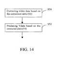
- FIG. 14is an exemplary flow chart for showing the operation of the system of FIG. 12 ;
- FIG. 15is an exemplary timing chart for showing the operation of the system of FIG. 12 ;
- FIG. 16is an exemplary flow chart for a hidden refresh operation of the system of FIG. 12 ;
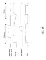
- FIG. 17is a diagram showing an example of a sample of the current/voltage correction curve
- FIG. 18is a diagram showing the current/voltage correction curve of FIG. 17 and an example of a newly measured data point:
- FIG. 19is a diagram showing an example of a new current/voltage correction curve based on the measured point of FIG. 18 ;
- FIG. 20is a block diagram showing a further example of a programming circuit for implementing a combined current and voltage-programming technique
- FIG. 21is a block diagram showing a system for driving an AMOLED display in accordance with a further embodiment of the invention.
- FIG. 22is a schematic diagram showing an example of a switch network of FIG. 21 ;
- FIG. 23is a schematic diagram showing a system for correcting the current/voltage information of the pixel circuit.
- Embodiments of the present inventionare described using an AMOLED display. Drive scheme described below is applicable to a current programmed (driven) pixel circuit and a voltage programmed (driven) pixel circuit.
- hybrid technique described belowcan be applied to any existing driving scheme, including a) any drive schemes that use sophisticated timing of the data, select, or power inputs to the pixels to achieve increased brightness uniformity, b) any drive schemes that use current or voltage feedback, c) any drive schemes that use optical feedback.
- the light emitting material of the pixel circuitcan be any technology, specifically organic light emitting diode (OLED) technology, and in particular, but not limited to, fluorescent, phosphorescent, polymer, and dendrimer materials.
- OLEDorganic light emitting diode
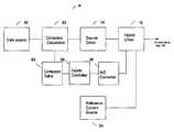
- FIG. 1there is illustrated a system 2 for driving an AMOLED display 5 in accordance with an embodiment of the present invention.
- the AMOLED display 5includes a plurality of pixel circuits.
- FIG. 1four pixel circuits 10 are shown as an example.
- the system 2includes a hybrid driving circuit 12 , a voltage source driver 14 , a hybrid programming controller 16 , a gate driver 18 A and a power-supply 18 B.
- the pixel circuit 10is selected by the gate driver 18 A (Vsel), and is programmed by either voltage mode using a node Vdata or current mode using a node Idata.
- the hybrid driving circuit 12selects the mode of programming, and connects it to the pixel circuit 10 through a hybrid signal.
- a pre-charge signal (Vp)is applied to the pixel circuit 10 to acquire threshold Vt information (or Vt shift information) from the pixel circuit 10 .
- the hybrid driving circuit 12controls the pre-charging, if pre-charging technique is used.
- the pre-charge signal (Vp)may be generated within the hybrid driving circuit 12 , which depends on the operation condition.
- the power-supply 18 B (Vdd)supplies the current required to energize the display 5 and to monitor the power consumption of the display 5 .
- the hybrid controller 16controls the individual components that make up the entire hybrid programming circuit.
- the hybrid controller 16handles timing and controls the order in which the required functions occur.
- the hybrid controller 16may generate data Idata and supplied to the hybrid driving circuit 12 .
- the system 2may have a reference current source, and the Idata may be supplied under the control of the hybrid controller 16 .
- the hybrid driver 12may be implemented either as a switching matrix, or as the hybrid driving circuit(s) of FIG. 3, 6, 8 or 20 or combination thereof.
- Vdatarefers to data, a data signal, a data line or a node for supplying the data or data signal Vdata, or a voltage on the data line or the node.
- Idatarefers to data, a data signal, a data line or a node for supplying the data or data signal Idata, or a current on the data line or the node.
- Vprefers to a pre-charge signal, a pre-charge pulse, a pre-charge voltage for pre-charging/discharging, a line or a node for supplying the pre-charge signal, pre-charge pulse or pre-charge voltage Vp.
- Vselrefers to a pulse or a signal for selecting a pixel circuit or a line or a node for supplying the pulse or signal Vs.
- the terms “hybrid signal”, “hybrid signal node”, and “hybrid signal line”may be used interchangeably.
- the pixel circuit 10includes a plurality of TFTs, and an organic light emitting diode (OLED).
- the TFTmay be an n-type TFT or a p-type TFT.
- the TFTis, for example, but not limited to, an amorphous silicon (a-Si:H) based TFT, a polycrystalline silicon based TFT, a crystalline silicon based TFT, or an organic semiconductor based TFT.
- the OLEDmay be regular (P-I-N) stack or inverted (N-I-P) stack.
- the OLEDcan be located in the source or the drain of one or more driving TFTs.
- FIG. 2illustrates an example of the pixel circuit 10 of FIG. 1 .
- the pixel circuit of FIG. 2includes four thin film transistors (TFTs) 20 - 26 , a capacitor Cs 28 and an organic light emitter diode (OLED) 30 .
- the TFT (Tdrive) 26is a drive TFT that is connected to the OLED 30 and the capacitor Cs 28 .
- the pixel circuit of FIG. 2is selected by the select line Vsel, and is programmed by a data line DL.
- the data line DLis controlled by the hybrid signal output from the hybrid driving circuit 12 of FIG. 1 .
- the pixel circuit 10 of FIG. 1may include less than four TFTs or more than four TFTs.
- data line DLand “data node DL” may be used interchangeably.
- the data node DLis pre-charged and discharged to acquire the threshold Vt of a drive TFT (e.g., Tdrive 26 of FIG. 2 ) or the threshold Vt shift.
- Vt shift, Vt shift information, Vt, and Vt informationmay be used interchangeably.
- the pixel circuit 10is then consecutively programmed by the source driver 14 using voltage-programming. The acquired Vt shift information is utilized to compensate for degradation of the pixel circuit 10 , thus maintaining uniform brightness of the display 5 .
- the process of acquiring Vtstarts by applying Vsel to T 1 20 and T 2 22 to the pixel circuit illustrated in FIG. 2 . Such action causes the drain and gate of T 3 24 to be at the same voltage. This allows the Vt of T 3 24 to be extracted by first applying the pre-charge voltage Vp to the data line DL, which is than allowed to be discharged.
- the rate of dischargeis a function of Vt. Thus, by measure of the rate of discharge, Vt can be obtained.
- FIG. 3illustrates an example of a hybrid driving circuit, which is applicable to the hybrid driving circuit 12 of FIG. 1 .
- the hybrid driving circuit 12 A of FIG. 3implements voltage programming technique.
- the hybrid driving circuit 12 A of FIG. 3includes a charge programming capacitor Cc 32 .
- the charge programming capacitor Cc 32is provided between the data line Vdata and the data node DL.
- the pre-charge line Vpis also connected to the data node DL.
- the hybrid driving circuit 12 Ais provided to a pixel circuit 10 A having four TFTs (such as the pixel circuit of FIG. 2 ).
- the pixel circuit 10 Amay include more than four TFTs or less than four TFTs.
- the charge programming capacitor Cc 32is provided to program the pixel circuit 10 A with a voltage that is equal to the sum of threshold Vt of the TFT and Vdata, scaled by a constant K.
- the constantis determined by the voltage division network formed by the charge storage capacitor (e.g. Cs 28 of FIG. 2 ) and the charge programming capacitor Cc 32 .
- FIG. 4illustrates an exemplary flow chart for showing the operation of the hybrid driving circuit 12 A of FIG. 3 .
- pre-charge modeis enabled.
- a pixel circuitis selected and pre-charging (Vp) is started.
- Vt acquisition modeis enabled, and at step S 16 , discharging (Vp) starts.
- the Vt informationis acquired through Cc 32 .
- writing modeis enabled.
- FIG. 5illustrates an exemplary timing chart for showing the operation of the hybrid driving circuit 12 A of FIG. 3 .
- Vdata 0represents voltage at the data node (e.g. DL of FIG. 2 ) of the pixel circuit;
- Idata 0represents current at the data node (e.g. DL of FIG. 2 ) of the pixel circuit.
- the programming procedurestarts by selecting the pixel to be programmed with the pulse Vsel.
- the pre-charge pulse Vpis applied to the pixel circuit's data input (e.g. DL of FIG. 2 ).
- Vt acquisition phasevoltage on the data line (DL) is allowed to be discharged through the pixel circuit, which is in a current mirror connection with the Vsel line held high.
- the data line (DL)is discharged to a certain voltage, and the Vt of a drive TFT is extracted from that voltage.
- the voltage at Vdatais at ground.
- the calculated compensated voltageis applied to the data input line (DL) of the pixel circuit.
- the programming routinefinishes with the lowering of the Vsel signal.
- the calculated compensated voltageis obtained through analog means of a charge programming capacitor Cc 32 .
- any other analog means for obtaining compensated voltagemay be used.
- any (external) digital circuite.g. 50 of FIG. 7 ) may be used to obtain the calculated compensated voltage.
- the source driver ( 14 of FIG. 1 )supplies Vdata to the capacitor Cc 32 .
- Vdatais increased from ground to the desired voltage level, the voltage at Idata is equal to (Vt+Vdata)*K.
- FIG. 3The structure of FIG. 3 is simple, and is easily implemented.
- FIG. 6illustrates a further example of a hybrid driving circuit, which is applicable to the hybrid driving circuit 12 of FIG. 1 .
- the hybrid driving circuit 12 B of FIG. 6implements voltage programming technique.
- the hybrid driving circuit 12 Bincludes a summer 40 , a sample and hold (S/H) circuit 42 and a switching element 44 .
- the S/H circuit 42samples Idata and holds it for a certain period.
- the summer 40receives Vdata and the output of the S/H circuit 42 .
- the switching element 44connects the output of the summer 40 to the data node DL in response to a programming control signal 46 .
- the hybrid driving circuit 12 Butilizes the summer 40 , instead of the charge coupling capacitor Cc 32 , to produce programming voltage that is equal to the sum of Vt and Vdata.
- the hybrid driving circuit 12 Bdoes not utilize a capacity, programming voltage is not affected by the parasitic capacitance, and it has less charge feed-through effect.
- the hybrid driving circuit 12 Bdoes not utilize a charge storage capacitor, programming voltage is not affected by the charge storage capacitance.
- the hybrid driving circuit 12 Bdoes not utilize a charge programming capacitor, it achieves faster Vt acquisition time. Removal of the charge programming capacitor eliminates the charge dependency of the programming scheme. Thus the programming voltage is not affected by the charge being shared between the charge storage capacitor and the parasitic capacitance of the system. This results in a higher effective programming voltage.
- FIG. 7illustrates an exemplary flow chart for showing the operation of the hybrid driving circuit 12 B of FIG. 6 .
- the Vtis sampled at step S 20 , and new data is produced at step S 22 .
- the new datais supplied to the pixel circuit in response to the programming control signal ( 46 ) at S 24 .
- the new datamay be produced after step S 18 .
- the control signal 46may be enabled before step S 18 .
- Vdatais at ground, and the voltage at the data node DL is equal to Vt of the TFT by the pre-charging/discharging operation (Vp).
- the voltage on the data node DLis sampled and holed by the S/H circuit 42 .
- the Vtis provided to the summer 40 through the S/H circuit 42 .
- the summer 40outputs the sum of Vt and Vdata.
- the switch 44turns on in response to the programming control signal 46 .
- FIG. 8illustrates a further example of a hybrid driving circuit, which is applicable to the hybrid driving circuit 12 of FIG. 1 .
- the hybrid driving circuit 12 C of FIG. 8implements voltage programming technique.
- the hybrid driving circuit 13 Cis a direct digital hybrid driving circuit.
- the direct digital programming circuit 13 Cincludes a microComputer uC 50 which receives digital data (Vdada), a digital to analog (D/A) converter 52 , a voltage follower 54 for increasing current without affecting voltage, and an analog to digital (A/D) converter 56 .
- the threshold Vt of the drive TFTmay increase slowly. Thus, it may not be necessary to acquire the threshold Vt of the drive TFT every programming cycle. This effectively hides the Vt acquisition for the majority of the programming cycle.
- the threshold Vt acquired from the pixel circuit 10 Ais digitalized at the A/D converter 56 , and is stored in memory contained in the uC 50 .
- the digital data that defines the brightness of the pixelis added to the Vt in the uC 50 .
- the resulting voltageis then converted back to an analog value at the D/A 52 , which is programmed into the pixel circuit 10 A.
- This programming methodis designed to compensate for the slow process of the Vt acquisition.
- FIG. 9illustrates an exemplary flow chart for showing the operation of the hybrid driving circuit 12 C of FIG. 8 .
- the Vt acquisition modethe Vt is sampled and recorded at step S 30 .
- writing modeWhen writing mode is enabled, new data is provided based on the recorded data. It is noted that the operation of the system having the hybrid driving circuit 12 C of FIG. 8 is not limited to FIG. 9 .
- the data which have been recordedmay be used without implementing the Vt acquisition.
- FIG. 10illustrates an exemplary timing chart for showing the operation of the hybrid driving circuit 12 C of FIG. 8 .
- the hybrid driving circuit 13 Cmay use the Vt that has been previously acquired and has been recorded in the uC 50 .
- the conversion of the output on the data node DL by A/Dcan remove the requirements of having to acquire the Vt every programming cycle.
- the Vt of the pixel circuit 10 Amay be acquired once every second or less. Thus, it may acquire Vt for only one row of the display per frame cycle. This effectively increases the amount of time for the pixel programming cycle. Less frequent need of Vt acquisition ensures faster programming time.
- FIG. 2is used to describe the pixel circuit 10 of FIG. 1 .
- the pixel circuit 10is not limited to that of FIG. 2 .
- the pixel circuit 10may be a pixel circuit illustrated in FIG. 11 (J. Kanichi, J.-H. Kim, J. Y. Nahm, Y. He and R. Hattori “Amorphous Silicon Thin-Film Transistor Based Active-Matrix Organic Light Emitting Display” Asia Display IDW 2001 pp. 315).
- the pixel circuit of FIG. 11includes four TFTs 64 - 70 , a capacitor C ST 72 and an OLED 74 .
- the TFT 78is a drive TFT that is connected to the OLED 74 and the capacitor C ST 72 .
- the pixel circuit of FIG. 11is selected by Vselect 1 and Vselect 2 , and is programmed by Idata.
- the voltage acquiredis a combination of the voltage across the OLED 74 and T 3 68 .
- the techniquecompensates the voltage change of both the Vt and the OLED 74 .
- Idata of FIG. 11corresponds to the data node DL of FIG. 2 .
- FIG. 12illustrates a system for driving an AMOLED display in accordance with a further embodiment of the invention.
- the system 82 of FIG. 12includes a hybrid programming circuit having a correction table 80 , a source driver 14 for implementing a voltage-programming scheme and a reference current source 94 for implementing a current-programming scheme.
- the system 82drives a display having a plurality of pixel circuits using the voltage-programming scheme and the current-programming scheme.
- a hybrid controller 98is provided to control each component.
- the hybrid controller 98is placed between the A/D converter 96 and the correction table 80 , as an example.
- the hybrid controller 98is similar to the hybrid controller 16 of FIG. 1 .
- the pixel circuit driven by the system 82may be the pixel circuit 10 of FIG. 1 , and may be a current programmed pixel circuit or a voltage programmed pixel circuit.
- the pixel circuit driven by the system 82may be implemented by FIG. 2 or FIG. 11 , however, is not limited to those of FIGS. 2 and 11 .
- the hybrid programming circuitincludes a correction calculation module 92 for correcting data from the data source 90 based on the correction table 80 and an A/D converter 96 .
- the data corrected by the correction calculation module 92is applied to the source driver 14 .
- the source driver 14generates Vdata based on the corrected data output from the correction calculation module 92 .
- Vdata from the source driver 14 and Idata from the reference current source 94are supplied to the hybrid driver 12 .
- the data source 90is, for example, but not limited to, a DVD.
- the hybrid driver 12may be implemented either as a switching matrix, or as the digital programming circuit(s) of FIG. 8, 20 or combination thereof.
- the A/D converter 96may be the A/D converter 56 of FIG. 8 .
- the system 82may implement the Vt acquisition technique described above using the A/D converter 96 ( 56 ).
- the correction table 80is a lookup table.
- the correction table 80records the relationship between current required to program the pixel circuit and voltage necessary to obtain that current.
- the correction table 80is built for every pixel in the entire display.
- the correction table 80is illustrated separately from the correction calculation module 92 . However, the correction table 80 may be included in the correction calculation module 92 .
- the operation of the system of FIG. 12has two modes, namely display mode and calibration mode.
- the display modethe data from the data source 90 is corrected using the data in the correction table 80 , and is applied to the source driver 14 .
- the hybrid driver 12is not involved in the display mode.
- the calibration modethe current from the reference current source 94 is applied to the pixel circuit, and the voltage associated with the current is read from the pixel circuit. The voltage is converted to a digital data by the A/D converter 96 .
- the correction table 80is updated with the correct value based on the digital data.
- a voltage-programming schemeis implemented.
- the voltage on the data line (e.g. DL of FIG. 2 ) of the pixel circuitdetermines the brightness of the pixels.
- the voltage required to program the pixel circuitis calculated from the pixel brightness to be displayed (from the incoming video information) combined with the current/voltage correction information stored in the correction table 80 .
- the information on the correction table 80is combined with incoming video information to ensure that each pixel will maintain a constant brightness over long-term use.
- the current source 94is connected to the data input node (DL) of the pixel circuit via the hybrid driver 12 .
- Each pixelis programmed through a current-programming scheme (where the level of current on the data line determines the brightness of the pixel), and the voltage required to achieve that current is read by the A/D converter 96 .
- the voltage required to program the pixel currentis sampled at multiple current points by the A/D converter 96 .
- the multiple pointsmay be a subset of the possible current levels (e.g. 256 possible levels for 8-bit, or 64 levels for 6-bit). This subset of voltage measurements is used to construct the correction table 80 that is interpolated from the measurement points.
- the calibration modemay be entered either through user's command or may be combined with the normal display mode so that the calibration takes place during the display refresh period.
- the entire displaymay be calibrated at once.
- the displaymay stop showing incoming video information for a short period of time while each pixel was programmed with a current and the voltage recorded.
- a subset of the pixelsmay be calibrated, such as one pixel every fixed number of frames. This is virtually transparent to the user, and the correction information may still be acquired for each pixel.
- the table lookup techniquecombines the technique of the current-programming scheme with the technique of the voltage-programming scheme.
- the pixel circuitis programmed with a current through a current-programming scheme. A voltage to maintain that current is read and is stored at a lookup table. The next time that particular level of current is applied to the pixel circuit, instead of programming with a current, the pixel circuit is programmed based on information on the lookup table. Accordingly, it attains the compensation inherent in the current programming scheme while attaining the fast programming time that is only possible with voltage-programming scheme.
- the correction table (lookup table) 80is used to correct the current/voltage correction information.
- the system 82 of FIG. 12may use the lookup table to correct the Vt shift and the current/voltage correction information at the same time in combination with the hybrid driving circuit of FIG. 3, 6, 8 or 20 .
- the hybrid controller 98extracts the Vt shift information by extending the voltage versus current curve to zero current point.
- the Vt shift informationis stored in an array of tables (correction table 80 ) which is applied to incoming display data.
- the uC 50 of FIG. 8 or 20may utilize the lookup table to generate appropriate voltage and program the pixel circuit.
- the hybrid circuits 12 A of FIGS. 3 and 12B of FIG. 6may be integrated into the system of FIG. 12 .
- FIGS. 13-14illustrate exemplary flow charts for showing the operation of the system of FIG. 12 .
- calibration modeis enabled.
- a pixel circuitis selected and current programming is implemented to the selected pixel circuit.
- a switch matrix enable signalis enabled. Then the connection to the pixel circuit is changed.
- the Vtis sampled at step s 46 , and then the correction table is created/corrected at step S 48 .
- video dataare corrected based on the correction table.
- new Vdatais produced based on the corrected data.
- the writing modemay be implemented based on the previously created correction table without implementing the calibration mode. It is noted that the operation of the system of FIG. 12 is not limited to FIGS. 13-14 .
- FIG. 15illustrates an exemplary timing chart for showing a combination of the Vt shift acquisition and the current/voltage correction.
- a switch matrix enable signal in FIG. 15represents a control signal for the hybrid driver 12 of FIG. 12 .
- the calibration modei.e. the current-programming scheme
- the programming modei.e. the voltage-programming scheme
- the calibration modemay be enabled when the switch matrix enable signal is low.
- the programming modemay be enabled when the switch matrix enable signal is high.
- A/D samplingis implemented during the calibration mode.
- the current from the reference current source 94is applied to the pixel circuit.
- the voltage on the data input nodeis converted to a digital voltage by the A/D converter 56 .
- current/voltage correction informationis recorded at the lookup table.
- the Vt shift informationis generated based on the data in the correction table 80 or the output from the A/D converter 96 .
- the system 82 of FIG. 12may implement hidden refresh technique for refreshing current/voltage correction information in addition to the table lookup technique described above.
- new current/voltage correction informationis constructed while completely hidden from user's perception.
- This techniqueutilizes the information that is currently displayed on the screen (i.e. the incoming video data).
- the current/voltage correction information for each pixel in the displayis known.
- the current/voltage correction curvemay shift due to the change in Vt.
- a new current/voltage correction curveis extrapolated from the point so that it is fitted to the measured point. Based on the new current/voltage correction curve, the Vt shift information is extracted which is used to compensate for the shift in Vt.
- FIG. 16illustrates an exemplary flow chart for the hidden refresh operation of the system of FIG. 12 .
- a current/voltage correction curveis produced during the calibration process that is implemented during the manufacturing of the display (step S 62 ).
- FIG. 17illustrates an example of a sample of the current voltage correction curve.
- the next stepis to measure a point along the curve during the usage of the display.
- This pointcan be any point along the curve, so any data that the user currently has on the display can be used for calibration (step S 64 ).
- FIG. 18illustrates the current voltage correction of FIG. 17 and an example of a newly measured data point.
- the last stepis to shift the current/voltage correction curve to fit the point of voltage verses current relationship that is measured (step S 66 ).
- FIG. 19illustrates an example of a new current voltage correction curve based on the measured point of FIG. 18 .
- FIGS. 17-19The process associated with FIGS. 17-19 is implemented in the hybrid controller 98 of FIG. 12 .
- the system 82 of FIG. 12may implement a combined current and voltage-programming technique.
- FIG. 20illustrates one example of a hybrid driving circuit for implementing the combined current and voltage-programming technique.
- the hybrid driving circuit of FIG. 20may be included in the hybrid driver 12 of FIG. 12 .
- the digital hybrid driving circuit 12 C and a current source 100are provided to the data line DL of the pixel circuit.
- the pixel circuit programmingis divided into two phases.
- the pixel circuit 10 Ais voltage-programmed first to set the gate voltage of the driving TFT to an approximate value, then followed by a current programming phase.
- the current programming phasecan then fine-tune the output current.
- the system of FIG. 20is faster than current programming and has the compensation capabilities of the current programming scheme.
- the digital hybrid driving circuit 12 Cis provided.
- the combined current and voltage-programming techniquemay be implemented by combining the hybrid driving circuit 12 A of FIG. 3 or 12B of FIG. 6 with the current source 100 .
- the current source 100may be the reference current source 94 of FIG. 12 .
- the system 2 of FIG. 1may implement the hidden refresh technique described above.
- the system 2 of FIG. 1may implement the combined current and voltage-programming technique.
- the system 2 of FIG. 1may include the hybrid driving circuit of FIG. 20 to implement the combined current and voltage-programming technique.
- the direct digital programming scheme( FIGS. 6, 8 and 20 ) can be extended to drive an OLED array (e.g. a 4T OLED array) using voltage programmed column drivers, such as those used for driving Active Matrix Liquixd Crystal Display (AMLCD), or voltage-programmed Active-Matrix Organic Light Emitting Diode (AMOLED) displays, or any other voltage-output display driver.
- AMLCDActive Matrix Liquixd Crystal Display
- AMOLEDActive-Matrix Organic Light Emitting Diode
- FIG. 21illustrates a system for driving an AMOLED array having a plurality of pixel circuits in accordance with a further embodiment of the invention.
- the system 105 of FIG. 21includes a voltage column driver 112 , a programmable current source 114 , a switching network 116 , an A/D converter 118 and a row driver 120 .
- the voltage column driver 112is a voltage programmed column driver.
- Each of the voltage column driver 112 and the row driver 120may be any driver that has a voltage output, such as those designed for the AMLCD.
- the voltage column driver 112 and the programmable current source 114are connected to an OLED array 110 through the switching network 116 .
- the OLED array 110forms an AMOLED display, and contains a plurality of pixel circuits (such as 10 of FIG. 1 ).
- the pixel circuitmay be a current programmed pixel circuit or a voltage programmed pixel circuit.
- the A/D converter 118is an interface that allows an analog signal (i.e. current driving the display 110 ) to be read back as a digital signal.
- the digital signal associated with the currentcan than be processed and/or stored.
- the A/D converter 118may be the A/D converter 56 of FIGS. 8 and 20 .
- the column driver 112may be the source driver 14 of FIGS. 1 and 12 .
- the system 105 of FIG. 21implements the calibration mode and the display mode as described above.
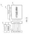
- FIG. 22illustrates an example of the switch network 116 of FIG. 21 .
- the switching network 116 of FIG. 22includes two MOSFET switches 122 and 124 that can switch the column of the display ( 110 ) from connecting to the column driver ( 112 ) to the combination of the current source ( 114 ) and the A/D converter ( 118 ), and vice versa.
- a shift register 126is a source of the digital control signal that controls the operation of the MOS switches 122 and 124 .
- An inverter 128inverts an output from the shift register 126 . Thus, when the switch 122 is on (off), the switch 124 is off (on).
- the switching network 116may be located either off the glass in the column driver ( 112 ) or directly on the glass using TFT switches.
- the system 105uses only one current source 114 .
- the voltage-programming drivers(such as, AMLCD drivers, or any other voltage-output drivers) drive the rest of the display 110 .
- the switching matrix(switching network 116 ) allows different pixels within the array of pixels to be connected to a single current source ( 114 ) through a time division method. This allows a single current source to be applied to the entire display. This lowers the cost of the driver circuit and speeds up the programming time for the pixel circuit.
- the system 105uses the A/D converter 118 to convert an analog output of the data node (e.g. DL of FIG. 2 ) of the pixel circuit to digital data.
- the conversion by the A/D converter 118removes the requirements of having to acquire the Vt every programming cycle.
- the Vt of the pixel circuitmay be acquired once every few minutes. Thus it may acquire one column of the panel every refresh cycle.
- Only one A/D 118may be implemented for all the columns.
- the circuitacquires only one pixel per frame refresh. For example, for a 320 by 240 panel, the number of pixels is 76, 8000. For a frame rate of 30 Hz, the time required to acquire Vt from all pixels for the entire frame is 43 minutes. This may be acceptable for some applications, providing that Vt does not shift substantially in an hour.
- the parasiticsonly affect the amount of time to discharge the capacitor to acquire Vt. Since the circuit is voltage-programmed, it is not affected by the parasitics. Since Vt is only acquired one column per frame time, it can be long. For example, for a display with 320 columns that has a frame rate of 30 Hz, each frame time is 33 mS. For voltage programming, it is possible to program a pixel in 70 uS. For 320 columns, the time to update the display is 22 mS, which still leave 11 mS to complete a charge/discharge cycle.
- the system 105may implement the lookup table technique to compensate for Vt shift and/or to correct the current/voltage information as described above
- the system 105may implement the hidden refresh technique to acquire the Vt shift information and current/voltage correction information of each pixel circuit ( 10 ) in the display 110 .
- This current/voltage correction informationis used to populate a lookup table (e.g. a correction table 80 of FIG. 12 ) that will then be used to compensate for the degradation in the pixel circuit, which is caused by aging.
- a lookup tablee.g. a correction table 80 of FIG. 12
- the system 105may implement the combined current and voltage-programming technique as described above.
- FIG. 23illustrates a system for correcting the current/voltage information of the pixel circuit.
- a display 130is depicted as a 2T or 4T OLED array.
- the display 130may include a plurality of pixel circuits, each having three or more than four transistors.
- the display 130may include voltage-driven pixel circuits or current-driven pixel circuits.
- the system of FIG. 23is applicable to the systems 2 , 82 and 105 of FIGS. 1, 12 and 22 .
- a switch 132is provided to disconnect the common electrode of the OLED. It is well known that two electrodes are provided for the OLED. One is connected to the pixel circuit, and the other is a common electrode connected to all OLEDs. It is noted that the common electrode may be Vdd or GND depending on the type of OLED.
- the switch 132connects the common electrode of the OLED into a current sensing network 134 utilizing a high side common mode sensor (such as, INA168 by TI). The current sensing network 134 measures the current through the common electrode.
- each pixelis lit individually and the current consumed is acquired by the sensing network 134 .
- the acquired currentis used to correct the lookup table (e.g. the correction table 80 of FIG. 12 ) populated by the direct digital hybrid driving circuit of FIG. 8 or 20 .
- a dark display currentmay be acquired to include the effect of dead pixel and leakage current of the array. During this procedure, all pixels are turned off, and the current (i.e. dark display current) is measured.
- the major issue with current-programmed pixel circuitswhich is the slow programming time, is solved.
- the concept of using feedback to compensate the pixel circuitenhances the uniformity and stability of the display while retaining the fast programming capability of the voltage programmed drive scheme.
Landscapes
- Engineering & Computer Science (AREA)
- Physics & Mathematics (AREA)
- Computer Hardware Design (AREA)
- General Physics & Mathematics (AREA)
- Theoretical Computer Science (AREA)
- Control Of Indicators Other Than Cathode Ray Tubes (AREA)
- Control Of El Displays (AREA)
- Electroluminescent Light Sources (AREA)
Abstract
Description
Notice: More than one reissue application has been filed for the reissue of U.S. Pat. No. 8,232,939. The reissue applications are (1) Ser. No. 14/090,320, which is an application for reissue of U.S. Pat. No. 8,232,939 and has been reissued as U.S. Pat. No. RE45,291 E, (2) application Ser. No. 14/326,705 (the present application), which is a continuation reissue of U.S. Pat. No. 8,232,939, and (3) application Ser. No. 14/326,677, which is a divisional reissue of U.S. Pat. No. 8,232,939.
This is a continuation of U.S. patent application Ser. No. 11/571,480, which is a national stage application of international application no. PCT/CA2005/001007, filed Jun. 28, 2005, which claims the benefit of and priority to Canadian Patent Application No. 2,472,671, filed on Jun. 29, 2004, each of these applications being incorporated herein by reference in its entirety.
The present invention relates to a display technique, and more specifically to technology for driving pixel circuits.
Active matrix organic light emitting diode (AMOLED) displays are well known in the art. The AMOLED displays have been increasingly used as a flat panel in a wide variety of tools.
The AMOLED displays are classified as either a voltage-programmed display or a current-programmed display. The voltage-programmed display is driven by a voltage-programmed scheme where data is applied to the display as a voltage. The current-programmed display is driven by a current-programmed scheme where data is applied to the display as a current.
The advantage of the current-programming scheme is that it can facilitate pixel designs where the brightness of the pixel remains more constant over time than with voltage programming. However, the current-programming requires longer time of charging capacitors associated with the column.
Therefore, there is a need to provide a new scheme for driving a current-driven AMOLED display, which ensures high speed and high quality.
The present invention relates to a system and method of driving a pixel circuit in an AMOLED display.
The system and method of the present invention uses Voltage-Programming Scheme For Current-Driven AMOLED Displays.
In accordance with an aspect of the present invention there is provided a system for driving a display which includes a plurality of pixel circuits, each having a plurality of thin film transistors (TFTs) and an organic light emitting diode (OLED), which includes: a voltage driver for generating a voltage to program the pixel circuit; a programmable current source for generating a current to program the pixel circuit; and a switching network for selectively connecting the data driver or the current source to one or more pixel circuits.
In accordance with a further aspect of the present invention there is provided a system for driving a pixel circuit having a plurality of thin film transistors (TFTs) and an organic light emitting diode (OLED), which includes: a pre-charge controller for pre-charging and discharging a data node of the pixel circuit to acquire threshold voltage information of the TFT from the data node; and a hybrid driving circuit for programming the pixel circuit based on the acquired threshold voltage information and video data information displayed on the pixel circuit.
In accordance with a further aspect of the present invention there is provided a system for driving a pixel circuit having a plurality of thin film transistors (TFTs) and an organic light emitting diode (OLED), which includes: a sampler for sampling, from a data node of the pixel circuit, a voltage required to program the pixel circuit; and a programming circuit for programming the pixel circuit based on the sampled voltage and video data information displayed on the pixel circuit.
In accordance with a further aspect of the present invention there is provided a method of driving a pixel circuit having a plurality of thin film transistors (TFTs) and an organic light emitting diode (OLED), which includes the steps of: selecting a pixel circuit and pre-charging a data node of the pixel circuit; allowing the pre-charged data node to be discharged; extracting a threshold voltage of the TFT through the discharging step; and programming the pixel circuit, including compensating a programming data based on the extracted threshold voltage.
This summary of the invention does not necessarily describe all features of the invention.
These and other features of the invention will become more apparent from the following description in which reference is made to the appended drawings wherein:
Embodiments of the present invention are described using an AMOLED display. Drive scheme described below is applicable to a current programmed (driven) pixel circuit and a voltage programmed (driven) pixel circuit.
In addition, hybrid technique described below can be applied to any existing driving scheme, including a) any drive schemes that use sophisticated timing of the data, select, or power inputs to the pixels to achieve increased brightness uniformity, b) any drive schemes that use current or voltage feedback, c) any drive schemes that use optical feedback.
The light emitting material of the pixel circuit can be any technology, specifically organic light emitting diode (OLED) technology, and in particular, but not limited to, fluorescent, phosphorescent, polymer, and dendrimer materials.
Referring toFIG. 1 , there is illustrated a system2 for driving anAMOLED display 5 in accordance with an embodiment of the present invention. TheAMOLED display 5 includes a plurality of pixel circuits. InFIG. 1 , fourpixel circuits 10 are shown as an example.
The system2 includes ahybrid driving circuit 12, avoltage source driver 14, ahybrid programming controller 16, agate driver 18A and a power-supply 18B. Thepixel circuit 10 is selected by thegate driver 18A (Vsel), and is programmed by either voltage mode using a node Vdata or current mode using a node Idata. Thehybrid driving circuit 12 selects the mode of programming, and connects it to thepixel circuit 10 through a hybrid signal. A pre-charge signal (Vp) is applied to thepixel circuit 10 to acquire threshold Vt information (or Vt shift information) from thepixel circuit 10. Thehybrid driving circuit 12 controls the pre-charging, if pre-charging technique is used. The pre-charge signal (Vp) may be generated within thehybrid driving circuit 12, which depends on the operation condition. The power-supply 18B (Vdd) supplies the current required to energize thedisplay 5 and to monitor the power consumption of thedisplay 5.
Thehybrid controller 16 controls the individual components that make up the entire hybrid programming circuit. Thehybrid controller 16 handles timing and controls the order in which the required functions occur. Thehybrid controller 16 may generate data Idata and supplied to thehybrid driving circuit 12. The system2 may have a reference current source, and the Idata may be supplied under the control of thehybrid controller 16.
Thehybrid driver 12 may be implemented either as a switching matrix, or as the hybrid driving circuit(s) ofFIG. 3, 6, 8 or 20 or combination thereof.
In the description, Vdata refers to data, a data signal, a data line or a node for supplying the data or data signal Vdata, or a voltage on the data line or the node. Similarly, Idata refers to data, a data signal, a data line or a node for supplying the data or data signal Idata, or a current on the data line or the node. Vp refers to a pre-charge signal, a pre-charge pulse, a pre-charge voltage for pre-charging/discharging, a line or a node for supplying the pre-charge signal, pre-charge pulse or pre-charge voltage Vp. Vsel refers to a pulse or a signal for selecting a pixel circuit or a line or a node for supplying the pulse or signal Vs. The terms “hybrid signal”, “hybrid signal node”, and “hybrid signal line” may be used interchangeably.
Thepixel circuit 10 includes a plurality of TFTs, and an organic light emitting diode (OLED). The TFT may be an n-type TFT or a p-type TFT. The TFT is, for example, but not limited to, an amorphous silicon (a-Si:H) based TFT, a polycrystalline silicon based TFT, a crystalline silicon based TFT, or an organic semiconductor based TFT. The OLED may be regular (P-I-N) stack or inverted (N-I-P) stack. The OLED can be located in the source or the drain of one or more driving TFTs.
InFIG. 2 , four TFTs are illustrated. However, thepixel circuit 10 ofFIG. 1 may include less than four TFTs or more than four TFTs.
In the description, the terms “data line DL” and “data node DL” may be used interchangeably.
Referring toFIGS. 1-2 , the data node DL is pre-charged and discharged to acquire the threshold Vt of a drive TFT (e.g.,Tdrive 26 ofFIG. 2 ) or the threshold Vt shift. In the description, Vt shift, Vt shift information, Vt, and Vt information may be used interchangeably. Thepixel circuit 10 is then consecutively programmed by thesource driver 14 using voltage-programming. The acquired Vt shift information is utilized to compensate for degradation of thepixel circuit 10, thus maintaining uniform brightness of thedisplay 5.
The process of acquiring Vt starts by applying Vsel toT1 20 andT2 22 to the pixel circuit illustrated inFIG. 2 . Such action causes the drain and gate ofT3 24 to be at the same voltage. This allows the Vt ofT3 24 to be extracted by first applying the pre-charge voltage Vp to the data line DL, which is than allowed to be discharged. The rate of discharge is a function of Vt. Thus, by measure of the rate of discharge, Vt can be obtained.
Thehybrid driving circuit 12A ofFIG. 3 includes a chargeprogramming capacitor Cc 32. The chargeprogramming capacitor Cc 32 is provided between the data line Vdata and the data node DL. The pre-charge line Vp is also connected to the data node DL.
Thehybrid driving circuit 12A is provided to apixel circuit 10A having four TFTs (such as the pixel circuit ofFIG. 2 ). However, thepixel circuit 10A may include more than four TFTs or less than four TFTs.
The chargeprogramming capacitor Cc 32 is provided to program thepixel circuit 10A with a voltage that is equal to the sum of threshold Vt of the TFT and Vdata, scaled by a constant K. The constant is determined by the voltage division network formed by the charge storage capacitor (e.g. Cs28 ofFIG. 2 ) and the chargeprogramming capacitor Cc 32.
The programming procedure starts by selecting the pixel to be programmed with the pulse Vsel. At the same time, the pre-charge pulse Vp is applied to the pixel circuit's data input (e.g. DL ofFIG. 2 ).
During the Vt acquisition phase, voltage on the data line (DL) is allowed to be discharged through the pixel circuit, which is in a current mirror connection with the Vsel line held high. The data line (DL) is discharged to a certain voltage, and the Vt of a drive TFT is extracted from that voltage. The voltage at Vdata is at ground.
During the programming (writing) phase, the calculated compensated voltage is applied to the data input line (DL) of the pixel circuit. The programming routine finishes with the lowering of the Vsel signal.
The calculated compensated voltage is obtained through analog means of a charge programming capacitor Cc32. However, any other analog means for obtaining compensated voltage may be used. Further, any (external) digital circuit (e.g.50 ofFIG. 7 ) may be used to obtain the calculated compensated voltage.
The source driver (14 ofFIG. 1 ) supplies Vdata to thecapacitor Cc 32. When Vdata is increased from ground to the desired voltage level, the voltage at Idata is equal to (Vt+Vdata)*K.
The structure ofFIG. 3 is simple, and is easily implemented.
Thehybrid driving circuit 12B includes asummer 40, a sample and hold (S/H)circuit 42 and a switchingelement 44. The S/H circuit 42 samples Idata and holds it for a certain period. Thesummer 40 receives Vdata and the output of the S/H circuit 42. The switchingelement 44 connects the output of thesummer 40 to the data node DL in response to aprogramming control signal 46.
Thehybrid driving circuit 12B utilizes thesummer 40, instead of the chargecoupling capacitor Cc 32, to produce programming voltage that is equal to the sum of Vt and Vdata. As thehybrid driving circuit 12B does not utilize a capacity, programming voltage is not affected by the parasitic capacitance, and it has less charge feed-through effect. As thehybrid driving circuit 12B does not utilize a charge storage capacitor, programming voltage is not affected by the charge storage capacitance. As thehybrid driving circuit 12B does not utilize a charge programming capacitor, it achieves faster Vt acquisition time. Removal of the charge programming capacitor eliminates the charge dependency of the programming scheme. Thus the programming voltage is not affected by the charge being shared between the charge storage capacitor and the parasitic capacitance of the system. This results in a higher effective programming voltage.
During the Vt acquisition cycle, Vdata is at ground, and the voltage at the data node DL is equal to Vt of the TFT by the pre-charging/discharging operation (Vp). The voltage on the data node DL is sampled and holed by the S/H circuit 42. The Vt is provided to thesummer 40 through the S/H circuit 42. When Vdata is increased from ground to the desired voltage level, thesummer 40 outputs the sum of Vt and Vdata. Theswitch 44 turns on in response to theprogramming control signal 46. The voltage at the data node DL goes to (Vt+Vdata). Timing chart for showing the operation of the system2 having thehybrid driving circuit 12B is similar to that ofFIG. 5 .
The hybrid driving circuit13C is a direct digital hybrid driving circuit. The direct digital programming circuit13C includes amicroComputer uC 50 which receives digital data (Vdada), a digital to analog (D/A)converter 52, avoltage follower 54 for increasing current without affecting voltage, and an analog to digital (A/D)converter 56.
The threshold Vt of the drive TFT may increase slowly. Thus, it may not be necessary to acquire the threshold Vt of the drive TFT every programming cycle. This effectively hides the Vt acquisition for the majority of the programming cycle. In the direct digital hybrid driving circuit13C, the threshold Vt acquired from thepixel circuit 10A is digitalized at the A/D converter 56, and is stored in memory contained in theuC 50. The digital data that defines the brightness of the pixel is added to the Vt in theuC 50. The resulting voltage is then converted back to an analog value at the D/A 52, which is programmed into thepixel circuit 10A. This programming method is designed to compensate for the slow process of the Vt acquisition.
The conversion of the output on the data node DL by A/D can remove the requirements of having to acquire the Vt every programming cycle. The Vt of thepixel circuit 10A may be acquired once every second or less. Thus, it may acquire Vt for only one row of the display per frame cycle. This effectively increases the amount of time for the pixel programming cycle. Less frequent need of Vt acquisition ensures faster programming time.
In the above description,FIG. 2 is used to describe thepixel circuit 10 ofFIG. 1 . However, thepixel circuit 10 is not limited to that ofFIG. 2 . Thepixel circuit 10 may be a pixel circuit illustrated inFIG. 11 (J. Kanichi, J.-H. Kim, J. Y. Nahm, Y. He and R. Hattori “Amorphous Silicon Thin-Film Transistor Based Active-Matrix Organic Light Emitting Display” Asia Display IDW 2001 pp. 315). The pixel circuit ofFIG. 11 includes four TFTs64-70, acapacitor C ST72 and anOLED 74. The TFT78 is a drive TFT that is connected to theOLED 74 and thecapacitor C ST72. The pixel circuit ofFIG. 11 is selected by Vselect1 and Vselect2, and is programmed by Idata. The voltage acquired is a combination of the voltage across theOLED 74 andT3 68. The technique compensates the voltage change of both the Vt and theOLED 74. Idata ofFIG. 11 corresponds to the data node DL ofFIG. 2 .
Ahybrid controller 98 is provided to control each component. InFIG. 12 , thehybrid controller 98 is placed between the A/D converter 96 and the correction table80, as an example. Thehybrid controller 98 is similar to thehybrid controller 16 ofFIG. 1 .
The pixel circuit driven by thesystem 82 may be thepixel circuit 10 ofFIG. 1 , and may be a current programmed pixel circuit or a voltage programmed pixel circuit. The pixel circuit driven by thesystem 82 may be implemented byFIG. 2 orFIG. 11 , however, is not limited to those ofFIGS. 2 and 11 .
The hybrid programming circuit includes acorrection calculation module 92 for correcting data from thedata source 90 based on the correction table80 and an A/D converter 96. The data corrected by thecorrection calculation module 92 is applied to thesource driver 14. Thesource driver 14 generates Vdata based on the corrected data output from thecorrection calculation module 92. Vdata from thesource driver 14 and Idata from the referencecurrent source 94 are supplied to thehybrid driver 12.
Thedata source 90 is, for example, but not limited to, a DVD. Thehybrid driver 12 may be implemented either as a switching matrix, or as the digital programming circuit(s) ofFIG. 8, 20 or combination thereof. The A/D converter 96 may be the A/D converter 56 ofFIG. 8 . Thesystem 82 may implement the Vt acquisition technique described above using the A/D converter96 (56).
The correction table80 is a lookup table. The correction table80 records the relationship between current required to program the pixel circuit and voltage necessary to obtain that current. The correction table80 is built for every pixel in the entire display.
In the description, the relationship between the current required to program the pixel circuit and the voltage necessary to obtain that programming current, is referred to as “current/voltage correction information”, “current/voltage correction curve”, or “current/voltage information”, or “current voltage curve”.
InFIG. 12 , the correction table80 is illustrated separately from thecorrection calculation module 92. However, the correction table80 may be included in thecorrection calculation module 92.
The operation of the system ofFIG. 12 has two modes, namely display mode and calibration mode. In the display mode, the data from thedata source 90 is corrected using the data in the correction table80, and is applied to thesource driver 14. Thehybrid driver 12 is not involved in the display mode. In the calibration mode, the current from the referencecurrent source 94 is applied to the pixel circuit, and the voltage associated with the current is read from the pixel circuit. The voltage is converted to a digital data by the A/D converter 96. The correction table80 is updated with the correct value based on the digital data.
During the display mode, a voltage-programming scheme is implemented. The voltage on the data line (e.g. DL ofFIG. 2 ) of the pixel circuit determines the brightness of the pixels. The voltage required to program the pixel circuit is calculated from the pixel brightness to be displayed (from the incoming video information) combined with the current/voltage correction information stored in the correction table80. The information on the correction table80 is combined with incoming video information to ensure that each pixel will maintain a constant brightness over long-term use.
After the display has been used for a fixed period of time, the display enters the calibration mode. Thecurrent source 94 is connected to the data input node (DL) of the pixel circuit via thehybrid driver 12. Each pixel is programmed through a current-programming scheme (where the level of current on the data line determines the brightness of the pixel), and the voltage required to achieve that current is read by the A/D converter 96.
The voltage required to program the pixel current is sampled at multiple current points by the A/D converter 96. The multiple points may be a subset of the possible current levels (e.g. 256 possible levels for 8-bit, or 64 levels for 6-bit). This subset of voltage measurements is used to construct the correction table80 that is interpolated from the measurement points.
The calibration mode may be entered either through user's command or may be combined with the normal display mode so that the calibration takes place during the display refresh period.
In one example, the entire display may be calibrated at once. The display may stop showing incoming video information for a short period of time while each pixel was programmed with a current and the voltage recorded.
In a further example, a subset of the pixels may be calibrated, such as one pixel every fixed number of frames. This is virtually transparent to the user, and the correction information may still be acquired for each pixel.
When a conventional voltage-programming scheme is utilized, a pixel circuit is programmed in an open loop configuration, where there is no feedback from the pixel circuit regarding the threshold voltage shift of the TFTs. When a conventional current-programming scheme is utilized, the brightness of the pixel may remain constant over time. However, the current programming scheme is slow. Thus, the table lookup technique combines the technique of the current-programming scheme with the technique of the voltage-programming scheme. The pixel circuit is programmed with a current through a current-programming scheme. A voltage to maintain that current is read and is stored at a lookup table. The next time that particular level of current is applied to the pixel circuit, instead of programming with a current, the pixel circuit is programmed based on information on the lookup table. Accordingly, it attains the compensation inherent in the current programming scheme while attaining the fast programming time that is only possible with voltage-programming scheme.
In the above description, the correction table (lookup table)80 is used to correct the current/voltage correction information. However, thesystem 82 ofFIG. 12 may use the lookup table to correct the Vt shift and the current/voltage correction information at the same time in combination with the hybrid driving circuit ofFIG. 3, 6, 8 or 20 .
For example, several voltage measurements are captured at many different current points by the A/D converter96 (56). Thehybrid controller 98 extracts the Vt shift information by extending the voltage versus current curve to zero current point. The Vt shift information is stored in an array of tables (correction table80) which is applied to incoming display data.
TheuC 50 ofFIG. 8 or 20 may utilize the lookup table to generate appropriate voltage and program the pixel circuit.
Thehybrid circuits 12A ofFIGS. 3 and 12B ofFIG. 6 may be integrated into the system ofFIG. 12 .
It is noted that the writing mode may be implemented based on the previously created correction table without implementing the calibration mode. It is noted that the operation of the system ofFIG. 12 is not limited toFIGS. 13-14 .
Referring toFIGS. 12 and 15 , the calibration mode (i.e. the current-programming scheme) is enabled when the switch matrix enable signal is high. The programming mode (i.e. the voltage-programming scheme) is enabled when the switch matrix enable signal is low. However, the calibration mode may be enabled when the switch matrix enable signal is low. The programming mode may be enabled when the switch matrix enable signal is high.
A/D sampling is implemented during the calibration mode. During the calibration mode, the current from the referencecurrent source 94 is applied to the pixel circuit. The voltage on the data input node is converted to a digital voltage by the A/D converter 56. Based on the digital voltage and current associated with the digital voltage, current/voltage correction information is recorded at the lookup table. The Vt shift information is generated based on the data in the correction table80 or the output from the A/D converter 96.
Thesystem 82 ofFIG. 12 may implement hidden refresh technique for refreshing current/voltage correction information in addition to the table lookup technique described above.
Under the hidden refresh operation, new current/voltage correction information is constructed while completely hidden from user's perception. This technique utilizes the information that is currently displayed on the screen (i.e. the incoming video data). By obtaining the pixel characteristics from the full calibration routine that has been performed during the manufacturing process of the display, the current/voltage correction information for each pixel in the display is known. During the display's usage, the current/voltage correction curve may shift due to the change in Vt. By measuring a single point along the current/voltage correction curve (which is the data currently displayed, that is part of the video image), a new current/voltage correction curve is extrapolated from the point so that it is fitted to the measured point. Based on the new current/voltage correction curve, the Vt shift information is extracted which is used to compensate for the shift in Vt.
Referring toFIG. 16 , the next step is to measure a point along the curve during the usage of the display. This point can be any point along the curve, so any data that the user currently has on the display can be used for calibration (step S64).FIG. 18 illustrates the current voltage correction ofFIG. 17 and an example of a newly measured data point.
Referring toFIG. 16 , the last step is to shift the current/voltage correction curve to fit the point of voltage verses current relationship that is measured (step S66).FIG. 19 illustrates an example of a new current voltage correction curve based on the measured point ofFIG. 18 .
The process associated withFIGS. 17-19 is implemented in thehybrid controller 98 ofFIG. 12 .
Thesystem 82 ofFIG. 12 may implement a combined current and voltage-programming technique.FIG. 20 illustrates one example of a hybrid driving circuit for implementing the combined current and voltage-programming technique. The hybrid driving circuit ofFIG. 20 may be included in thehybrid driver 12 ofFIG. 12 .
In the hybrid driving circuit ofFIG. 20 , the digitalhybrid driving circuit 12C and acurrent source 100 are provided to the data line DL of the pixel circuit.
To enhance the circuit's ability to compensate for a change in the current/voltage correction curve due to temperature, threshold voltage shift, or other factors, the pixel circuit programming is divided into two phases.
During the writing mode, thepixel circuit 10A is voltage-programmed first to set the gate voltage of the driving TFT to an approximate value, then followed by a current programming phase. The current programming phase can then fine-tune the output current. The system ofFIG. 20 is faster than current programming and has the compensation capabilities of the current programming scheme.
InFIG. 20 , the digitalhybrid driving circuit 12C is provided. However, the combined current and voltage-programming technique may be implemented by combining thehybrid driving circuit 12A ofFIG. 3 or 12B ofFIG. 6 with thecurrent source 100. Thecurrent source 100 may be the referencecurrent source 94 ofFIG. 12 .
The system2 ofFIG. 1 may implement the hidden refresh technique described above. The system2 ofFIG. 1 may implement the combined current and voltage-programming technique. The system2 ofFIG. 1 may include the hybrid driving circuit ofFIG. 20 to implement the combined current and voltage-programming technique.
Extension of the direct digital programming scheme is now described in detail. The direct digital programming scheme (FIGS. 6, 8 and 20 ) can be extended to drive an OLED array (e.g. a 4T OLED array) using voltage programmed column drivers, such as those used for driving Active Matrix Liquixd Crystal Display (AMLCD), or voltage-programmed Active-Matrix Organic Light Emitting Diode (AMOLED) displays, or any other voltage-output display driver.
Thevoltage column driver 112 is a voltage programmed column driver. Each of thevoltage column driver 112 and therow driver 120 may be any driver that has a voltage output, such as those designed for the AMLCD. Thevoltage column driver 112 and the programmablecurrent source 114 are connected to anOLED array 110 through theswitching network 116. TheOLED array 110 forms an AMOLED display, and contains a plurality of pixel circuits (such as10 ofFIG. 1 ). The pixel circuit may be a current programmed pixel circuit or a voltage programmed pixel circuit.
The A/D converter 118 is an interface that allows an analog signal (i.e. current driving the display110) to be read back as a digital signal. The digital signal associated with the current can than be processed and/or stored. The A/D converter 118 may be the A/D converter 56 ofFIGS. 8 and 20 . Thecolumn driver 112 may be thesource driver 14 ofFIGS. 1 and 12 .
Thesystem 105 ofFIG. 21 implements the calibration mode and the display mode as described above.
Theswitching network 116 may be located either off the glass in the column driver (112) or directly on the glass using TFT switches.
Referring toFIGS. 21-22 , thesystem 105 uses only onecurrent source 114. The voltage-programming drivers (such as, AMLCD drivers, or any other voltage-output drivers) drive the rest of thedisplay 110. The switching matrix (switching network116) allows different pixels within the array of pixels to be connected to a single current source (114) through a time division method. This allows a single current source to be applied to the entire display. This lowers the cost of the driver circuit and speeds up the programming time for the pixel circuit.
Thesystem 105 uses the A/D converter 118 to convert an analog output of the data node (e.g. DL ofFIG. 2 ) of the pixel circuit to digital data. The conversion by the A/D converter 118 removes the requirements of having to acquire the Vt every programming cycle. The Vt of the pixel circuit may be acquired once every few minutes. Thus it may acquire one column of the panel every refresh cycle.
Only one A/D 118 may be implemented for all the columns. The circuit acquires only one pixel per frame refresh. For example, for a 320 by 240 panel, the number of pixels is 76, 8000. For a frame rate of 30 Hz, the time required to acquire Vt from all pixels for the entire frame is 43 minutes. This may be acceptable for some applications, providing that Vt does not shift substantially in an hour.
The parasitics only affect the amount of time to discharge the capacitor to acquire Vt. Since the circuit is voltage-programmed, it is not affected by the parasitics. Since Vt is only acquired one column per frame time, it can be long. For example, for a display with 320 columns that has a frame rate of 30 Hz, each frame time is 33 mS. For voltage programming, it is possible to program a pixel in 70 uS. For 320 columns, the time to update the display is 22 mS, which still leave 11 mS to complete a charge/discharge cycle.
Thesystem 105 may implement the lookup table technique to compensate for Vt shift and/or to correct the current/voltage information as described above
Thesystem 105 may implement the hidden refresh technique to acquire the Vt shift information and current/voltage correction information of each pixel circuit (10) in thedisplay 110. This current/voltage correction information is used to populate a lookup table (e.g. a correction table80 ofFIG. 12 ) that will then be used to compensate for the degradation in the pixel circuit, which is caused by aging. To reduce cost, the number of current-programmed circuits has been reduced so there is only one per display instead of one per column driver.
Thesystem 105 may implement the combined current and voltage-programming technique as described above.
The current/voltage information of the pixel circuit can be further corrected by implementing a system illustrated inFIG. 23 .FIG. 23 illustrates a system for correcting the current/voltage information of the pixel circuit. InFIG. 23 , adisplay 130 is depicted as a 2T or 4T OLED array. However, thedisplay 130 may include a plurality of pixel circuits, each having three or more than four transistors. Thedisplay 130 may include voltage-driven pixel circuits or current-driven pixel circuits. The system ofFIG. 23 is applicable to thesystems FIGS. 1, 12 and 22 .
As illustrated inFIG. 23 , aswitch 132 is provided to disconnect the common electrode of the OLED. It is well known that two electrodes are provided for the OLED. One is connected to the pixel circuit, and the other is a common electrode connected to all OLEDs. It is noted that the common electrode may be Vdd or GND depending on the type of OLED. Theswitch 132 connects the common electrode of the OLED into acurrent sensing network 134 utilizing a high side common mode sensor (such as, INA168 by TI). Thecurrent sensing network 134 measures the current through the common electrode.
During the calibration phase, each pixel is lit individually and the current consumed is acquired by thesensing network 134. The acquired current is used to correct the lookup table (e.g. the correction table80 ofFIG. 12 ) populated by the direct digital hybrid driving circuit ofFIG. 8 or 20 .
A dark display current may be acquired to include the effect of dead pixel and leakage current of the array. During this procedure, all pixels are turned off, and the current (i.e. dark display current) is measured.
According to the embodiments of the present invention, the major issue with current-programmed pixel circuits, which is the slow programming time, is solved. The concept of using feedback to compensate the pixel circuit enhances the uniformity and stability of the display while retaining the fast programming capability of the voltage programmed drive scheme.
The present invention has been described with regard to one or more embodiments. However, it will be apparent to persons skilled in the art that a number of variations and modifications can be made without departing from the scope of the invention as defined in the claims.
Claims (35)
1. A system for programming at least one pixel circuit in a display, the system comprising:
a voltage driver for generating a voltage to apply to a data node of the at least one pixel circuit to thereby program the at least one pixel circuit according to the generated voltage;
a programmable current source for providing a first current and a second current to apply to the data node of the at least one pixel circuit;
a sampler for reading a first voltage on the data node while the first current is maintained through the at least one pixel circuit via the programmable current source and for reading a second voltage on the data node while the second current is maintained through the at least one pixel circuit via the programmable current source; and
a controller configured to:
generate a voltage versus current relationship for the at least one pixel circuit based on the first current and the second current and based on the sampled first and second voltages,
extract, based on the voltage versus current relationship for the at least one pixel circuit, a voltage corresponding to a zero current level, and
program the at least one pixel circuit via the data node with a programming voltage generated by the voltage driver that is set according to display data and according to the extracted voltage corresponding to the zero current level.
2. The system according toclaim 1 , wherein the at least one pixel circuit is configured to be alternately programmed by a programming current applied to the data node or by a programming voltage applied to the data node.
3. The system according toclaim 2 , wherein the at least one pixel circuit includes a mirror transistor having a gate coupled to a gate terminal of the driving transistor, the at least one pixel circuit configured such that the data node is coupled to a gate terminal of the mirror transistor via one or more switch transistors, the applied current being conveyed via the one or more switch transistors through the mirror transistor while the gate terminal of the mirror transistor adjusts to a voltage for maintaining the applied current through the mirror transistor.
4. The system according toclaim 3 , wherein the one or more switch transistors include a first switch transistor and a second transistor,
the first switch transistor operated according to a select signal and configured to couple the data node to the gate terminal of the mirror transistor while the first switch transistor is switched on,
the second switch transistor operated according to the select signal and configured to couple the data node to a drain or a source terminal of the mirror transistor while the second switch transistor is switched on.
5. The system according toclaim 2 , wherein the at least one pixel circuit includes one or more switch transistors configured to couple the data node to a drain or a source terminal of the driving transistor while the programming current is applied to the at least one pixel circuit via the data node,
the one or more switch transistors further configured to couple the data node to a gate terminal of the driving transistor while the programming current is applied, such that the gate terminal of the driving transistor adjusts to a voltage for maintaining the applied current through the driving transistor,
the one or more switch transistors further configured to couple the data node to a gate terminal of the driving transistor while the programming voltage is applied to the at least one pixel circuit via the data node.
6. The system according toclaim 1 , wherein the sampler includes an analog to digital converter configured to capture digital information indicative of the first and second voltages on the data node.
7. The system according toclaim 6 , further comprising a memory for storing the digital information indicative of the first and second voltages, the digital information being stored in a lookup table that associates the first and second voltages with the first and second currents to thereby characterize the voltage versus current relationship of the at least one pixel circuit.
8. The system according toclaim 1 , wherein the controller is further configured to instruct the voltage driver to set the programming voltage for the at least one pixel circuit by adding the voltage corresponding to the zero current level to a voltage indicated by the display data.
9. The system according toclaim 1 , wherein the at least one pixel circuit is a plurality of pixel circuits arranged in an array of rows and columns, each of the plurality of pixel circuits having a data node coupled to a data line, and wherein the programmable current source is configured to generate a plurality currents to apply to each of the plurality of pixel circuits and the sampler is configured to read a corresponding plurality of voltages for each of the plurality of pixel circuits while each of the plurality of currents is maintained through respective ones of the plurality of pixel circuits.
10. The system according toclaim 1 , wherein the controller is configured to extract the threshold voltage of the driving transistor of the at least one pixel circuit by extending the voltage versus current relationship for the at least one pixel circuit to the zero current level and determining the voltage corresponding to the zero current level, the voltage corresponding to the zero current level providing an estimate of the threshold voltage of the driving transistor of the at least one pixel circuit.
11. The system according toclaim 1 , further comprising a memory communicatively coupled to the controller for digitally storing digital information indicative of the first and second voltages.
12. The system according toclaim 1 , wherein the at least one pixel circuit includes an organic light emitting diode for emitting light according to the display data and one or more thin film transistors for conveying a current through the organic light emitting diode according to the display data.
13. A method of operating a display having at least one pixel circuit, the at least one pixel circuit having a light emitting device coupled in series with a driving transistor configured to convey a driving current through the light emitting device according to display information, the at least one pixel circuit configured to be alternately programmed according to the display information by a programming current applied to a data node of the at least one pixel circuit or by a programming voltage applied to the data node, the method comprising:
applying a first current to the data node of the at least one pixel circuit;
reading a first voltage on the data node while the first current is maintained through the at least one pixel circuit;
applying a second current to the data node of the at least one pixel circuit;
reading a second voltage on the data node while the second current is maintained through the at least one pixel circuit;
storing digital information indicative of the first and second voltages such that the first and second voltages are associated with the first and second currents;
generating a voltage versus current relationship for the at least one pixel circuit based on the first and second voltages and the first and second currents;
extracting, based on the generated voltage versus current relationship for the at least one pixel circuit, a voltage corresponding to a zero current level; and
programming the at least one pixel circuit by applying, to the data node of the at least one pixel circuit, a programming voltage that is based on the display data and the voltage corresponding to the zero current level.
14. The method according toclaim 13 , wherein the at least one pixel circuit is at least one of a plurality of pixel circuits arranged in an array of rows and columns in the display, and wherein the applying the first and second current, the reading the first and second voltages, the storing, the generating, and the extracting are applied to each of the plurality of pixel circuits such that voltages corresponding to the zero current level are extracted for each of the plurality of pixel circuits.
15. The method according toclaim 14 , wherein the voltage corresponding to the zero current level is an estimate of a threshold voltage of the driving transistor in the at least one pixel circuit, and wherein the programming is applied to each of the plurality of pixel circuits based on the display data for each of the plurality of pixel circuits and based on the estimate of the threshold voltage of the driving transistor for each of the plurality of pixel circuits such that the display is operated to compensate for the threshold voltages of the driving transistors in each of the plurality of pixel circuits.
16. The method according toclaim 13 , wherein the storing is carried out by digitally storing the digital information indicative of the first and second voltages in a lookup table associated with the at least one pixel circuit.
17. The method according toclaim 13 , wherein the applying the first current and the applying the second current are performed during a calibration mode of the display that is distinct from a normal display mode, the calibration mode being a period during which images are not shown on the display.
18. The method according toclaim 13 , wherein at least one of the first current or the second current is a programming current applied to the at least one pixel circuit during a programming operation of a normal display mode to program the at least one pixel circuit to emit light according to the display information.
19. The method according toclaim 13 , wherein the at least one pixel circuit is at least one of a plurality of pixel circuits arranged in an array of rows and columns in the display, and wherein at least one of the first current or the second current is a programming current applied to the at least one pixel circuit during a programming operation of a normal display mode while others of the plurality of pixel circuits are voltage programmed with programming voltages, thereby hiding the applying the at least one of the first current or the second current to the at least one pixel circuit.
20. The method according toclaim 13 , further comprising:
responsive to the extracting, applying a third current to the data node of the at least one pixel circuit;
reading a third voltage on the data node while the third current is maintained through the at least one pixel circuit;
storing digital information indicative of the third voltage such that the third voltage is associated with the third current;
updating the voltage versus current relationship for the at least one pixel circuit based on at least the third voltage and the third current;
extracting, based on the updated voltage versus current relationship for the at least one pixel circuit, a voltage corresponding to a zero current level, the voltage corresponding to the zero current level being an updated estimate of a threshold voltage of the driving transistor in the at least one pixel circuit; and
programming the at least one pixel circuit to compensate for the threshold voltage of the driving transistor by applying, to the data node of the at least one pixel circuit, a programming voltage that is based on the display data and the updated estimated threshold voltage.
21. A system for programming at least one pixel circuit in a display, the system comprising:
a voltage driver for generating a voltage to apply to a data node of the at least one pixel circuit to thereby program the at least one pixel circuit according to the generated voltage;
a programmable current source for providing a first current to apply to the data node of the at least one pixel circuit;
a sampler for reading a first voltage on the data node while the first current is maintained through the at least one pixel circuit via the programmable current source; and
a controller configured to:
receive calibration data indicative of a voltage versus current relationship for the at least one pixel circuit;
generate an updated voltage versus current relationship for the at least one pixel circuit based on the first current and the first voltage and based on the received calibration data,
extract, based on the updated voltage versus current relationship for the at least one pixel circuit, a voltage corresponding to a zero current level, and
program the at least one pixel circuit via the data node with a programming voltage generated by the voltage driver that is set according to display data and according to the extracted voltage corresponding to the zero current level.
22. The system according toclaim 21 , wherein the first current is a programming current applied to the at least one pixel circuit during a programming operation of a normal display mode to program the at least one pixel circuit to emit light according to the display information.
23. The system according toclaim 21 , wherein the at least one pixel circuit is configured to be alternately programmed by a programming current applied to the data node or by a programming voltage applied to the data node.
24. The system according toclaim 21 , wherein the at least one pixel circuit is a plurality of pixel circuits arranged in an array of rows and columns, each of the plurality of pixel circuits having a data node coupled to a data line, and wherein the programmable current source is configured to generate a plurality currents to apply to each of the plurality of pixel circuits and the sampler is configured to read a corresponding plurality of voltages for each of the plurality of pixel circuits while each of the plurality of currents is maintained through respective ones of the plurality of pixel circuits.
25. The system according toclaim 21 , wherein the sampler includes an analog to digital converter configured to capture digital information indicative of the first and second voltages on the data node.
26. The system according toclaim 25 , further comprising a memory for storing the digital information indicative of the first voltage, the digital information being stored in a lookup table that associates the first voltage with the first current to thereby characterize the voltage versus current relationship of the at least one pixel circuit.
27. The system according toclaim 21 , wherein the at least one pixel circuit includes an organic light emitting diode for emitting light according to the display data and one or more thin film transistors for conveying a current through the organic light emitting diode according to the display data.
28. A method of operating a display having at least one pixel circuit, the at least one pixel circuit having a light emitting device coupled in series with a driving transistor configured to convey a driving current through the light emitting device according to display information, the at least one pixel circuit configured to be alternately programmed according to the display information by a programming current applied to a data node of the at least one pixel circuit or by a programming voltage applied to the data node, the method comprising:
applying a first current to the data node of the at least one pixel circuit;
reading a first voltage on the data node while the first current is maintained through the at least one pixel circuit;
storing digital information indicative of the first voltage such that the first voltage is associated with the first current;
receiving calibration data indicative of a voltage versus current relationship for the at least one pixel circuit;
generating an updated voltage versus current relationship for the at least one pixel circuit based on the first voltage, the first current, and the received calibration data;
extracting, based on the updated voltage versus current relationship for the at least one pixel circuit, a voltage corresponding to a zero current level; and
programming the at least one pixel circuit by applying, to the data node of the at least one pixel circuit, a programming voltage that is based on the display data and the voltage corresponding to the zero current level.
29. The method according toclaim 28 , wherein the at least one pixel circuit is at least one of a plurality of pixel circuits arranged in an array of rows and columns in the display, and wherein the applying the first current, the reading the first voltage, the storing, the receiving, the generating, and the extracting are applied to each of the plurality of pixel circuits such that voltages corresponding to the zero current level are extracted for each of the plurality of pixel circuits.
30. The method according toclaim 29 , wherein the voltage corresponding to the zero current level is an estimate of a threshold voltage of the driving transistor in the at least one pixel circuit, and wherein the programming is applied to each of the plurality of pixel circuits based on the display data for each of the plurality of pixel circuits and based on the estimate of the threshold voltage of the driving transistor for each of the plurality of pixel circuits such that the display is operated to compensate for the threshold voltages of the driving transistors in each of the plurality of pixel circuits.
31. A method of calibrating a display panel having a plurality of pixel circuits, each of the pixel circuits including a drive transistor coupled to an organic light emitting device, comprising:
measuring a degradation of each pixel circuit of a subset of the pixel circuits during a frame while displaying a video image with the pixel circuits on the display panel;
extracting, for each of the pixel circuits of the subset, a current/voltage point for the pixel circuit from the degradation measurement;
determining, for each of the pixel circuits of the subset, corresponding compensation information from a fitting of a previously stored voltage versus current relationship for the pixel circuit to the extracted current/voltage point for the pixel circuit; and
compensating each of the pixel circuits of the subset based on the respective compensation information for each of the pixel circuits of the subset.
32. The method of claim 31, wherein each of the pixel circuits are programmed using current, while the degradation measurement is a voltage measurement.
33. The method of claim 31, wherein the measuring is carried out without stopping video information from being displayed on the display panel.
34. The method of claim 33, wherein the measuring is carried out during a refresh period of the display panel.
35. The method of claim 31, wherein the measuring, extracting, and determining are carried out externally from the pixel circuit.
Priority Applications (1)
| Application Number | Priority Date | Filing Date | Title |
|---|---|---|---|
| US14/326,705USRE47257E1 (en) | 2004-06-29 | 2014-07-09 | Voltage-programming scheme for current-driven AMOLED displays |
Applications Claiming Priority (7)
| Application Number | Priority Date | Filing Date | Title |
|---|---|---|---|
| CA002472671ACA2472671A1 (en) | 2004-06-29 | 2004-06-29 | Voltage-programming scheme for current-driven amoled displays |
| CA2472671 | 2004-06-29 | ||
| PCT/CA2005/001007WO2006000101A1 (en) | 2004-06-29 | 2005-06-28 | Voltage-programming scheme for current-driven amoled displays |
| US12/571,480US20100015443A1 (en) | 2007-04-03 | 2009-10-01 | Adherence substance, pressure sensitive adhesive sheet and its use |
| US13/396,375US8232939B2 (en) | 2004-06-29 | 2012-02-14 | Voltage-programming scheme for current-driven AMOLED displays |
| US14/090,320USRE45291E1 (en) | 2004-06-29 | 2013-11-26 | Voltage-programming scheme for current-driven AMOLED displays |
| US14/326,705USRE47257E1 (en) | 2004-06-29 | 2014-07-09 | Voltage-programming scheme for current-driven AMOLED displays |
Related Parent Applications (1)
| Application Number | Title | Priority Date | Filing Date |
|---|---|---|---|
| US13/396,375ReissueUS8232939B2 (en) | 2004-06-29 | 2012-02-14 | Voltage-programming scheme for current-driven AMOLED displays |
Publications (1)
| Publication Number | Publication Date |
|---|---|
| USRE47257E1true USRE47257E1 (en) | 2019-02-26 |
Family
ID=35588998
Family Applications (4)
| Application Number | Title | Priority Date | Filing Date |
|---|---|---|---|
| US11/571,480Active2028-01-21US8115707B2 (en) | 2004-06-29 | 2005-06-28 | Voltage-programming scheme for current-driven AMOLED displays |
| US13/396,375CeasedUS8232939B2 (en) | 2004-06-29 | 2012-02-14 | Voltage-programming scheme for current-driven AMOLED displays |
| US14/090,320Expired - LifetimeUSRE45291E1 (en) | 2004-06-29 | 2013-11-26 | Voltage-programming scheme for current-driven AMOLED displays |
| US14/326,705Expired - LifetimeUSRE47257E1 (en) | 2004-06-29 | 2014-07-09 | Voltage-programming scheme for current-driven AMOLED displays |
Family Applications Before (3)
| Application Number | Title | Priority Date | Filing Date |
|---|---|---|---|
| US11/571,480Active2028-01-21US8115707B2 (en) | 2004-06-29 | 2005-06-28 | Voltage-programming scheme for current-driven AMOLED displays |
| US13/396,375CeasedUS8232939B2 (en) | 2004-06-29 | 2012-02-14 | Voltage-programming scheme for current-driven AMOLED displays |
| US14/090,320Expired - LifetimeUSRE45291E1 (en) | 2004-06-29 | 2013-11-26 | Voltage-programming scheme for current-driven AMOLED displays |
Country Status (7)
| Country | Link |
|---|---|
| US (4) | US8115707B2 (en) |
| EP (2) | EP1779365B1 (en) |
| JP (1) | JP5279265B2 (en) |
| CN (2) | CN102426822B (en) |
| CA (1) | CA2472671A1 (en) |
| TW (1) | TW200603057A (en) |
| WO (1) | WO2006000101A1 (en) |
Families Citing this family (153)
| Publication number | Priority date | Publication date | Assignee | Title |
|---|---|---|---|---|
| US7569849B2 (en) | 2001-02-16 | 2009-08-04 | Ignis Innovation Inc. | Pixel driver circuit and pixel circuit having the pixel driver circuit |
| CA2419704A1 (en) | 2003-02-24 | 2004-08-24 | Ignis Innovation Inc. | Method of manufacturing a pixel with organic light-emitting diode |
| CA2443206A1 (en) | 2003-09-23 | 2005-03-23 | Ignis Innovation Inc. | Amoled display backplanes - pixel driver circuits, array architecture, and external compensation |
| CA2472671A1 (en) | 2004-06-29 | 2005-12-29 | Ignis Innovation Inc. | Voltage-programming scheme for current-driven amoled displays |
| CA2490858A1 (en) | 2004-12-07 | 2006-06-07 | Ignis Innovation Inc. | Driving method for compensated voltage-programming of amoled displays |
| US9799246B2 (en) | 2011-05-20 | 2017-10-24 | Ignis Innovation Inc. | System and methods for extraction of threshold and mobility parameters in AMOLED displays |
| US10012678B2 (en) | 2004-12-15 | 2018-07-03 | Ignis Innovation Inc. | Method and system for programming, calibrating and/or compensating, and driving an LED display |
| TWI402790B (en) | 2004-12-15 | 2013-07-21 | Ignis Innovation Inc | Method and system for programming, calibrating and driving a light-emitting element display |
| US8576217B2 (en) | 2011-05-20 | 2013-11-05 | Ignis Innovation Inc. | System and methods for extraction of threshold and mobility parameters in AMOLED displays |
| US8599191B2 (en) | 2011-05-20 | 2013-12-03 | Ignis Innovation Inc. | System and methods for extraction of threshold and mobility parameters in AMOLED displays |
| US20140111567A1 (en) | 2005-04-12 | 2014-04-24 | Ignis Innovation Inc. | System and method for compensation of non-uniformities in light emitting device displays |
| US9275579B2 (en) | 2004-12-15 | 2016-03-01 | Ignis Innovation Inc. | System and methods for extraction of threshold and mobility parameters in AMOLED displays |
| US9280933B2 (en) | 2004-12-15 | 2016-03-08 | Ignis Innovation Inc. | System and methods for extraction of threshold and mobility parameters in AMOLED displays |
| US9171500B2 (en) | 2011-05-20 | 2015-10-27 | Ignis Innovation Inc. | System and methods for extraction of parasitic parameters in AMOLED displays |
| US10013907B2 (en) | 2004-12-15 | 2018-07-03 | Ignis Innovation Inc. | Method and system for programming, calibrating and/or compensating, and driving an LED display |
| CA2495726A1 (en) | 2005-01-28 | 2006-07-28 | Ignis Innovation Inc. | Locally referenced voltage programmed pixel for amoled displays |
| CA2496642A1 (en) | 2005-02-10 | 2006-08-10 | Ignis Innovation Inc. | Fast settling time driving method for organic light-emitting diode (oled) displays based on current programming |
| JP4852866B2 (en)* | 2005-03-31 | 2012-01-11 | カシオ計算機株式会社 | Display device and drive control method thereof |
| JP4798342B2 (en)* | 2005-03-31 | 2011-10-19 | カシオ計算機株式会社 | Display drive device and drive control method thereof, and display device and drive control method thereof |
| US7907137B2 (en) | 2005-03-31 | 2011-03-15 | Casio Computer Co., Ltd. | Display drive apparatus, display apparatus and drive control method thereof |
| JP2006317696A (en)* | 2005-05-12 | 2006-11-24 | Sony Corp | Pixel circuit, display device, and method for controlling pixel circuit |
| JP5355080B2 (en) | 2005-06-08 | 2013-11-27 | イグニス・イノベイション・インコーポレーテッド | Method and system for driving a light emitting device display |
| CA2510855A1 (en) | 2005-07-06 | 2007-01-06 | Ignis Innovation Inc. | Fast driving method for amoled displays |
| KR100703463B1 (en)* | 2005-08-01 | 2007-04-03 | 삼성에스디아이 주식회사 | Data driving circuit, organic light emitting display using same and driving method thereof |
| CA2518276A1 (en) | 2005-09-13 | 2007-03-13 | Ignis Innovation Inc. | Compensation technique for luminance degradation in electro-luminance devices |
| WO2007079572A1 (en) | 2006-01-09 | 2007-07-19 | Ignis Innovation Inc. | Method and system for driving an active matrix display circuit |
| US9489891B2 (en) | 2006-01-09 | 2016-11-08 | Ignis Innovation Inc. | Method and system for driving an active matrix display circuit |
| US9269322B2 (en) | 2006-01-09 | 2016-02-23 | Ignis Innovation Inc. | Method and system for driving an active matrix display circuit |
| TWI450247B (en) | 2006-02-10 | 2014-08-21 | Ignis Innovation Inc | Method and system for pixel circuit displays |
| TW200746022A (en) | 2006-04-19 | 2007-12-16 | Ignis Innovation Inc | Stable driving scheme for active matrix displays |
| TWI385621B (en)* | 2006-08-01 | 2013-02-11 | Casio Computer Co Ltd | Display drive apparatus and a drive method thereof, and display apparatus and the drive method thereof |
| JP4935979B2 (en)* | 2006-08-10 | 2012-05-23 | カシオ計算機株式会社 | Display device and driving method thereof, display driving device and driving method thereof |
| US8199074B2 (en)* | 2006-08-11 | 2012-06-12 | Chimei Innolux Corporation | System and method for reducing mura defects |
| CA2556961A1 (en) | 2006-08-15 | 2008-02-15 | Ignis Innovation Inc. | Oled compensation technique based on oled capacitance |
| JP5240542B2 (en)* | 2006-09-25 | 2013-07-17 | カシオ計算機株式会社 | Display driving device and driving method thereof, and display device and driving method thereof |
| JP4222426B2 (en) | 2006-09-26 | 2009-02-12 | カシオ計算機株式会社 | Display driving device and driving method thereof, and display device and driving method thereof |
| JP2008292834A (en)* | 2007-05-25 | 2008-12-04 | Hitachi Displays Ltd | Display device |
| US8405585B2 (en)* | 2008-01-04 | 2013-03-26 | Chimei Innolux Corporation | OLED display, information device, and method for displaying an image in OLED display |
| JP4715850B2 (en)* | 2008-01-15 | 2011-07-06 | ソニー株式会社 | Display device, driving method thereof, and electronic apparatus |
| KR100969769B1 (en)* | 2008-01-21 | 2010-07-13 | 삼성모바일디스플레이주식회사 | Organic light emitting display device and driving method thereof |
| EP2277163B1 (en) | 2008-04-18 | 2018-11-21 | Ignis Innovation Inc. | System and driving method for light emitting device display |
| CN101285848B (en)* | 2008-05-28 | 2010-06-02 | 炬力集成电路设计有限公司 | Method and device for correcting and obtaining reference voltage |
| CA2637343A1 (en) | 2008-07-29 | 2010-01-29 | Ignis Innovation Inc. | Improving the display source driver |
| US9370075B2 (en) | 2008-12-09 | 2016-06-14 | Ignis Innovation Inc. | System and method for fast compensation programming of pixels in a display |
| JP5239812B2 (en)* | 2008-12-11 | 2013-07-17 | ソニー株式会社 | Display device, display device driving method, and electronic apparatus |
| CA2669367A1 (en) | 2009-06-16 | 2010-12-16 | Ignis Innovation Inc | Compensation technique for color shift in displays |
| US9311859B2 (en) | 2009-11-30 | 2016-04-12 | Ignis Innovation Inc. | Resetting cycle for aging compensation in AMOLED displays |
| US9384698B2 (en) | 2009-11-30 | 2016-07-05 | Ignis Innovation Inc. | System and methods for aging compensation in AMOLED displays |
| CA2688870A1 (en) | 2009-11-30 | 2011-05-30 | Ignis Innovation Inc. | Methode and techniques for improving display uniformity |
| US10319307B2 (en) | 2009-06-16 | 2019-06-11 | Ignis Innovation Inc. | Display system with compensation techniques and/or shared level resources |
| US8379012B2 (en)* | 2009-07-17 | 2013-02-19 | Atmel Corporation | Selector switch for direct connection of switched regulator to voltage inputs |
| JP5503255B2 (en)* | 2009-11-10 | 2014-05-28 | グローバル・オーエルイーディー・テクノロジー・リミテッド・ライアビリティ・カンパニー | Pixel circuit, display device, and inspection method |
| US8497828B2 (en) | 2009-11-12 | 2013-07-30 | Ignis Innovation Inc. | Sharing switch TFTS in pixel circuits |
| US10996258B2 (en) | 2009-11-30 | 2021-05-04 | Ignis Innovation Inc. | Defect detection and correction of pixel circuits for AMOLED displays |
| CA2686174A1 (en) | 2009-12-01 | 2011-06-01 | Ignis Innovation Inc | High reslution pixel architecture |
| US8803417B2 (en) | 2009-12-01 | 2014-08-12 | Ignis Innovation Inc. | High resolution pixel architecture |
| CA2687631A1 (en) | 2009-12-06 | 2011-06-06 | Ignis Innovation Inc | Low power driving scheme for display applications |
| US9881532B2 (en) | 2010-02-04 | 2018-01-30 | Ignis Innovation Inc. | System and method for extracting correlation curves for an organic light emitting device |
| US10163401B2 (en) | 2010-02-04 | 2018-12-25 | Ignis Innovation Inc. | System and methods for extracting correlation curves for an organic light emitting device |
| CA2692097A1 (en) | 2010-02-04 | 2011-08-04 | Ignis Innovation Inc. | Extracting correlation curves for light emitting device |
| US10089921B2 (en) | 2010-02-04 | 2018-10-02 | Ignis Innovation Inc. | System and methods for extracting correlation curves for an organic light emitting device |
| US20140313111A1 (en) | 2010-02-04 | 2014-10-23 | Ignis Innovation Inc. | System and methods for extracting correlation curves for an organic light emitting device |
| US10176736B2 (en) | 2010-02-04 | 2019-01-08 | Ignis Innovation Inc. | System and methods for extracting correlation curves for an organic light emitting device |
| CA2696778A1 (en) | 2010-03-17 | 2011-09-17 | Ignis Innovation Inc. | Lifetime, uniformity, parameter extraction methods |
| DE102010019667B4 (en)* | 2010-04-28 | 2014-02-20 | Fraunhofer-Gesellschaft zur Förderung der angewandten Forschung e.V. | Circuit arrangement for arranged in a two-dimensional matrix organic light-emitting diodes |
| KR101101554B1 (en)* | 2010-08-19 | 2012-01-02 | 한국과학기술원 | Active organic light emitting display |
| US8907991B2 (en) | 2010-12-02 | 2014-12-09 | Ignis Innovation Inc. | System and methods for thermal compensation in AMOLED displays |
| JP5182382B2 (en)* | 2011-01-11 | 2013-04-17 | カシオ計算機株式会社 | Display device |
| JP5182383B2 (en)* | 2011-01-11 | 2013-04-17 | カシオ計算機株式会社 | Display device |
| US9606607B2 (en) | 2011-05-17 | 2017-03-28 | Ignis Innovation Inc. | Systems and methods for display systems with dynamic power control |
| US9886899B2 (en) | 2011-05-17 | 2018-02-06 | Ignis Innovation Inc. | Pixel Circuits for AMOLED displays |
| US9351368B2 (en) | 2013-03-08 | 2016-05-24 | Ignis Innovation Inc. | Pixel circuits for AMOLED displays |
| CN109272933A (en) | 2011-05-17 | 2019-01-25 | 伊格尼斯创新公司 | The method for operating display |
| US20140368491A1 (en) | 2013-03-08 | 2014-12-18 | Ignis Innovation Inc. | Pixel circuits for amoled displays |
| US9530349B2 (en) | 2011-05-20 | 2016-12-27 | Ignis Innovations Inc. | Charged-based compensation and parameter extraction in AMOLED displays |
| US9466240B2 (en) | 2011-05-26 | 2016-10-11 | Ignis Innovation Inc. | Adaptive feedback system for compensating for aging pixel areas with enhanced estimation speed |
| US9773439B2 (en) | 2011-05-27 | 2017-09-26 | Ignis Innovation Inc. | Systems and methods for aging compensation in AMOLED displays |
| US9881587B2 (en) | 2011-05-28 | 2018-01-30 | Ignis Innovation Inc. | Systems and methods for operating pixels in a display to mitigate image flicker |
| US9070775B2 (en) | 2011-08-03 | 2015-06-30 | Ignis Innovations Inc. | Thin film transistor |
| US8901579B2 (en) | 2011-08-03 | 2014-12-02 | Ignis Innovation Inc. | Organic light emitting diode and method of manufacturing |
| GB2495117A (en)* | 2011-09-29 | 2013-04-03 | Cambridge Display Tech Ltd | Display driver circuits for OLED displays |
| KR101536129B1 (en)* | 2011-10-04 | 2015-07-14 | 엘지디스플레이 주식회사 | Organic light-emitting display device |
| KR101463651B1 (en) | 2011-10-12 | 2014-11-20 | 엘지디스플레이 주식회사 | Organic light-emitting display device |
| CN102708788B (en)* | 2011-11-23 | 2015-01-07 | 京东方科技集团股份有限公司 | Pixel circuit |
| US9324268B2 (en) | 2013-03-15 | 2016-04-26 | Ignis Innovation Inc. | Amoled displays with multiple readout circuits |
| US10089924B2 (en) | 2011-11-29 | 2018-10-02 | Ignis Innovation Inc. | Structural and low-frequency non-uniformity compensation |
| US9385169B2 (en) | 2011-11-29 | 2016-07-05 | Ignis Innovation Inc. | Multi-functional active matrix organic light-emitting diode display |
| KR101362002B1 (en)* | 2011-12-12 | 2014-02-11 | 엘지디스플레이 주식회사 | Organic light-emitting display device |
| US8937632B2 (en) | 2012-02-03 | 2015-01-20 | Ignis Innovation Inc. | Driving system for active-matrix displays |
| US9190456B2 (en) | 2012-04-25 | 2015-11-17 | Ignis Innovation Inc. | High resolution display panel with emissive organic layers emitting light of different colors |
| US9747834B2 (en) | 2012-05-11 | 2017-08-29 | Ignis Innovation Inc. | Pixel circuits including feedback capacitors and reset capacitors, and display systems therefore |
| US8922544B2 (en) | 2012-05-23 | 2014-12-30 | Ignis Innovation Inc. | Display systems with compensation for line propagation delay |
| KR101528148B1 (en) | 2012-07-19 | 2015-06-12 | 엘지디스플레이 주식회사 | Organic light emitting diode display device having for sensing pixel current and method of sensing the same |
| US9786223B2 (en) | 2012-12-11 | 2017-10-10 | Ignis Innovation Inc. | Pixel circuits for AMOLED displays |
| US9336717B2 (en) | 2012-12-11 | 2016-05-10 | Ignis Innovation Inc. | Pixel circuits for AMOLED displays |
| US9830857B2 (en) | 2013-01-14 | 2017-11-28 | Ignis Innovation Inc. | Cleaning common unwanted signals from pixel measurements in emissive displays |
| CN108665836B (en) | 2013-01-14 | 2021-09-03 | 伊格尼斯创新公司 | Method and system for compensating for deviations of a measured device current from a reference current |
| US9721505B2 (en) | 2013-03-08 | 2017-08-01 | Ignis Innovation Inc. | Pixel circuits for AMOLED displays |
| CA2894717A1 (en) | 2015-06-19 | 2016-12-19 | Ignis Innovation Inc. | Optoelectronic device characterization in array with shared sense line |
| EP3043338A1 (en) | 2013-03-14 | 2016-07-13 | Ignis Innovation Inc. | Re-interpolation with edge detection for extracting an aging pattern for amoled displays |
| US9952698B2 (en) | 2013-03-15 | 2018-04-24 | Ignis Innovation Inc. | Dynamic adjustment of touch resolutions on an AMOLED display |
| WO2014174427A1 (en) | 2013-04-22 | 2014-10-30 | Ignis Innovation Inc. | Inspection system for oled display panels |
| TWI497472B (en)* | 2013-06-06 | 2015-08-21 | Au Optronics Corp | Pixel driving method of a display panel and display panel thereof |
| CN105474296B (en) | 2013-08-12 | 2017-08-18 | 伊格尼斯创新公司 | A method and device for driving a display using image data |
| KR102071690B1 (en) | 2013-08-19 | 2020-01-31 | 삼성디스플레이 주식회사 | Noise removing circuit and current sensing unit including the same |
| TW201508908A (en) | 2013-08-19 | 2015-03-01 | Chunghwa Picture Tubes Ltd | Pixel circuit of organic light emitting diode |
| KR102058577B1 (en) | 2013-09-13 | 2019-12-24 | 삼성디스플레이 주식회사 | Display device and driving method therof |
| KR102084711B1 (en) | 2013-10-10 | 2020-04-16 | 삼성디스플레이 주식회사 | Display deviceand driving method thereof |
| KR102109191B1 (en) | 2013-11-14 | 2020-05-12 | 삼성디스플레이 주식회사 | Organic light emitting display device and driving method thereof |
| KR102212424B1 (en) | 2013-11-18 | 2021-02-04 | 삼성디스플레이 주식회사 | Display deviceand driving method thereof |
| US9443469B2 (en) | 2013-11-22 | 2016-09-13 | Global Oled Technology Llc | Pixel circuit, driving method, display device, and inspection method |
| US9741282B2 (en) | 2013-12-06 | 2017-08-22 | Ignis Innovation Inc. | OLED display system and method |
| US9761170B2 (en) | 2013-12-06 | 2017-09-12 | Ignis Innovation Inc. | Correction for localized phenomena in an image array |
| US9502653B2 (en) | 2013-12-25 | 2016-11-22 | Ignis Innovation Inc. | Electrode contacts |
| US10997901B2 (en) | 2014-02-28 | 2021-05-04 | Ignis Innovation Inc. | Display system |
| US10176752B2 (en) | 2014-03-24 | 2019-01-08 | Ignis Innovation Inc. | Integrated gate driver |
| DE102015206281A1 (en) | 2014-04-08 | 2015-10-08 | Ignis Innovation Inc. | Display system with shared level resources for portable devices |
| TWI553609B (en) | 2014-08-26 | 2016-10-11 | 友達光電股份有限公司 | Display device and method for driving the same |
| KR102256069B1 (en) | 2014-09-03 | 2021-05-25 | 삼성디스플레이 주식회사 | Display device and calibration method thereof |
| KR102270460B1 (en) | 2014-09-19 | 2021-06-29 | 삼성디스플레이 주식회사 | Organic Light Emitting Display And Compensation Method Of Degradation |
| CA2872563A1 (en) | 2014-11-28 | 2016-05-28 | Ignis Innovation Inc. | High pixel density array architecture |
| KR102320300B1 (en) | 2014-12-01 | 2021-11-03 | 삼성디스플레이 주식회사 | Orgainic light emitting display |
| KR102320316B1 (en) | 2014-12-01 | 2021-11-02 | 삼성디스플레이 주식회사 | Orgainic light emitting display and driving method for the same |
| CA2873476A1 (en) | 2014-12-08 | 2016-06-08 | Ignis Innovation Inc. | Smart-pixel display architecture |
| CA2879462A1 (en) | 2015-01-23 | 2016-07-23 | Ignis Innovation Inc. | Compensation for color variation in emissive devices |
| CA2886862A1 (en) | 2015-04-01 | 2016-10-01 | Ignis Innovation Inc. | Adjusting display brightness for avoiding overheating and/or accelerated aging |
| CA2889870A1 (en) | 2015-05-04 | 2016-11-04 | Ignis Innovation Inc. | Optical feedback system |
| CA2892714A1 (en) | 2015-05-27 | 2016-11-27 | Ignis Innovation Inc | Memory bandwidth reduction in compensation system |
| CA2898282A1 (en) | 2015-07-24 | 2017-01-24 | Ignis Innovation Inc. | Hybrid calibration of current sources for current biased voltage progra mmed (cbvp) displays |
| US10657895B2 (en) | 2015-07-24 | 2020-05-19 | Ignis Innovation Inc. | Pixels and reference circuits and timing techniques |
| US10373554B2 (en) | 2015-07-24 | 2019-08-06 | Ignis Innovation Inc. | Pixels and reference circuits and timing techniques |
| KR102435923B1 (en) | 2015-08-05 | 2022-08-25 | 삼성디스플레이 주식회사 | Organic light emitting display device and method of driving the same |
| CA2900170A1 (en) | 2015-08-07 | 2017-02-07 | Gholamreza Chaji | Calibration of pixel based on improved reference values |
| CA2908285A1 (en) | 2015-10-14 | 2017-04-14 | Ignis Innovation Inc. | Driver with multiple color pixel structure |
| CA2909813A1 (en) | 2015-10-26 | 2017-04-26 | Ignis Innovation Inc | High ppi pattern orientation |
| FR3047340B1 (en) | 2016-02-02 | 2019-10-18 | Dassault Aviation | SYSTEM FOR AIDING THE AUTHORIZATION DECISION FROM AN AIRCRAFT, AND ASSOCIATED METHOD |
| US9961178B2 (en)* | 2016-03-24 | 2018-05-01 | Motorola Mobility Llc | Embedded active matrix organic light emitting diode (AMOLED) fingerprint sensor |
| TWI587265B (en)* | 2016-05-31 | 2017-06-11 | 瑞鼎科技股份有限公司 | Display driving apparatus |
| US9875797B1 (en)* | 2016-12-04 | 2018-01-23 | Alex Diggins | Photon memory system |
| US10586491B2 (en) | 2016-12-06 | 2020-03-10 | Ignis Innovation Inc. | Pixel circuits for mitigation of hysteresis |
| US10714018B2 (en) | 2017-05-17 | 2020-07-14 | Ignis Innovation Inc. | System and method for loading image correction data for displays |
| US11025899B2 (en) | 2017-08-11 | 2021-06-01 | Ignis Innovation Inc. | Optical correction systems and methods for correcting non-uniformity of emissive display devices |
| CN107622754B (en)* | 2017-09-22 | 2023-11-14 | 京东方科技集团股份有限公司 | Pixel circuit and control method thereof, display substrate, display device |
| CN107516483B (en)* | 2017-09-28 | 2020-06-30 | 京东方科技集团股份有限公司 | Electrical detection method and device for device faults and display module |
| US10971078B2 (en) | 2018-02-12 | 2021-04-06 | Ignis Innovation Inc. | Pixel measurement through data line |
| DE102019210555A1 (en)* | 2018-07-19 | 2020-01-23 | Ignis Innovation Inc. | Systems and methods for compensating for degradation of an OLED display |
| US11276348B2 (en)* | 2018-07-19 | 2022-03-15 | Ignis Innovation Inc. | Compensation systems and methods for OLED display degradation |
| CN111710304B (en)* | 2020-07-17 | 2021-12-07 | 京东方科技集团股份有限公司 | Pixel driving circuit, driving method thereof and display device |
| WO2022040879A1 (en)* | 2020-08-24 | 2022-03-03 | 华为技术有限公司 | Pixel driving circuit and micro light emitting diode display panel |
| KR20230142020A (en) | 2022-03-30 | 2023-10-11 | 삼성디스플레이 주식회사 | Light emitting display device |
| CN114677966B (en)* | 2022-04-19 | 2024-09-24 | 中南大学 | A Micro-LED display device and feedback compensation circuit thereof |
| CN117769734A (en) | 2022-06-30 | 2024-03-26 | 京东方科技集团股份有限公司 | Spliced display screen and display method thereof |
| CN115171607B (en)* | 2022-09-06 | 2023-01-31 | 惠科股份有限公司 | Pixel circuit, display panel and display device |
Citations (569)
| Publication number | Priority date | Publication date | Assignee | Title |
|---|---|---|---|---|
| US3506851A (en) | 1966-12-14 | 1970-04-14 | North American Rockwell | Field effect transistor driver using capacitor feedback |
| US3774055A (en) | 1972-01-24 | 1973-11-20 | Nat Semiconductor Corp | Clocked bootstrap inverter circuit |
| US4090096A (en) | 1976-03-31 | 1978-05-16 | Nippon Electric Co., Ltd. | Timing signal generator circuit |
| US4160934A (en) | 1977-08-11 | 1979-07-10 | Bell Telephone Laboratories, Incorporated | Current control circuit for light emitting diode |
| US4354162A (en) | 1981-02-09 | 1982-10-12 | National Semiconductor Corporation | Wide dynamic range control amplifier with offset correction |
| EP0158366A2 (en) | 1984-04-13 | 1985-10-16 | Sharp Kabushiki Kaisha | Color liquid-crystal display apparatus |
| US4758831A (en) | 1984-11-05 | 1988-07-19 | Kabushiki Kaisha Toshiba | Matrix-addressed display device |
| GB2205431A (en) | 1986-09-27 | 1988-12-07 | Junichi Nishizawa | Color display device |
| JPH01272298A (en) | 1988-04-25 | 1989-10-31 | Yamaha Corp | Driving device |
| US4943956A (en) | 1988-04-25 | 1990-07-24 | Yamaha Corporation | Driving apparatus |
| US4963860A (en) | 1988-02-01 | 1990-10-16 | General Electric Company | Integrated matrix display circuitry |
| US4975691A (en) | 1987-06-16 | 1990-12-04 | Interstate Electronics Corporation | Scan inversion symmetric drive |
| US4996523A (en) | 1988-10-20 | 1991-02-26 | Eastman Kodak Company | Electroluminescent storage display with improved intensity driver circuits |
| US5051739A (en) | 1986-05-13 | 1991-09-24 | Sanyo Electric Co., Ltd. | Driving circuit for an image display apparatus with improved yield and performance |
| CA1294034C (en) | 1985-01-09 | 1992-01-07 | Hiromu Hosokawa | Color uniformity compensation apparatus for cathode ray tubes |
| JPH0442619A (en) | 1990-06-08 | 1992-02-13 | Fujitsu Ltd | DA converter |
| JPH04158570A (en) | 1990-10-22 | 1992-06-01 | Seiko Epson Corp | Structure of semiconductor device and manufacture thereof |
| US5153420A (en) | 1990-11-28 | 1992-10-06 | Xerox Corporation | Timing independent pixel-scale light sensing apparatus |
| CA2109951A1 (en) | 1991-05-24 | 1992-11-26 | Robert Hotto | Dc integrating display driver employing pixel status memories |
| US5198803A (en) | 1990-06-06 | 1993-03-30 | Opto Tech Corporation | Large scale movie display system with multiple gray levels |
| US5204661A (en) | 1990-12-13 | 1993-04-20 | Xerox Corporation | Input/output pixel circuit and array of such circuits |
| US5206633A (en)* | 1991-08-19 | 1993-04-27 | International Business Machines Corp. | Self calibrating brightness controls for digitally operated liquid crystal display system |
| US5222082A (en) | 1991-02-28 | 1993-06-22 | Thomson Consumer Electronics, S.A. | Shift register useful as a select line scanner for liquid crystal display |
| US5266515A (en) | 1992-03-02 | 1993-11-30 | Motorola, Inc. | Fabricating dual gate thin film transistors |
| JPH06314977A (en) | 1993-04-28 | 1994-11-08 | Nec Ic Microcomput Syst Ltd | Current output type d/a converter circuit |
| WO1994025954A1 (en) | 1993-04-30 | 1994-11-10 | Prime View Hk Limited | Apparatus for recovery of threshold voltage shift in amorphous silicon thin-film transistor device |
| US5489918A (en) | 1991-06-14 | 1996-02-06 | Rockwell International Corporation | Method and apparatus for dynamically and adjustably generating active matrix liquid crystal display gray level voltages |
| US5498880A (en) | 1995-01-12 | 1996-03-12 | E. I. Du Pont De Nemours And Company | Image capture panel using a solid state device |
| US5572444A (en) | 1992-08-19 | 1996-11-05 | Mtl Systems, Inc. | Method and apparatus for automatic performance evaluation of electronic display devices |
| JPH08340243A (en) | 1995-06-14 | 1996-12-24 | Canon Inc | Bias circuit |
| US5589847A (en) | 1991-09-23 | 1996-12-31 | Xerox Corporation | Switched capacitor analog circuits using polysilicon thin film technology |
| JPH0990405A (en) | 1995-09-21 | 1997-04-04 | Sharp Corp | Thin film transistor |
| US5619033A (en) | 1995-06-07 | 1997-04-08 | Xerox Corporation | Layered solid state photodiode sensor array |
| US5648276A (en) | 1993-05-27 | 1997-07-15 | Sony Corporation | Method and apparatus for fabricating a thin film semiconductor device |
| US5670973A (en) | 1993-04-05 | 1997-09-23 | Cirrus Logic, Inc. | Method and apparatus for compensating crosstalk in liquid crystal displays |
| US5686935A (en) | 1995-03-06 | 1997-11-11 | Thomson Consumer Electronics, S.A. | Data line drivers with column initialization transistor |
| US5691783A (en) | 1993-06-30 | 1997-11-25 | Sharp Kabushiki Kaisha | Liquid crystal display device and method for driving the same |
| US5712653A (en) | 1993-12-27 | 1998-01-27 | Sharp Kabushiki Kaisha | Image display scanning circuit with outputs from sequentially switched pulse signals |
| US5714968A (en) | 1994-08-09 | 1998-02-03 | Nec Corporation | Current-dependent light-emitting element drive circuit for use in active matrix display device |
| US5723950A (en) | 1996-06-10 | 1998-03-03 | Motorola | Pre-charge driver for light emitting devices and method |
| US5745660A (en) | 1995-04-26 | 1998-04-28 | Polaroid Corporation | Image rendering system and method for generating stochastic threshold arrays for use therewith |
| US5744824A (en) | 1994-06-15 | 1998-04-28 | Sharp Kabushiki Kaisha | Semiconductor device method for producing the same and liquid crystal display including the same |
| US5748160A (en) | 1995-08-21 | 1998-05-05 | Mororola, Inc. | Active driven LED matrices |
| US5747928A (en) | 1994-10-07 | 1998-05-05 | Iowa State University Research Foundation, Inc. | Flexible panel display having thin film transistors driving polymer light-emitting diodes |
| JPH10153759A (en) | 1996-11-26 | 1998-06-09 | Matsushita Electric Ind Co Ltd | Liquid crystal display |
| US5784042A (en) | 1991-03-19 | 1998-07-21 | Hitachi, Ltd. | Liquid crystal display device and method for driving the same |
| CA2249592A1 (en) | 1997-01-28 | 1998-07-30 | Casio Computer Co., Ltd. | Active matrix electroluminescent display device and a driving method thereof |
| US5790234A (en) | 1995-12-27 | 1998-08-04 | Canon Kabushiki Kaisha | Eyeball detection apparatus |
| JPH10254410A (en) | 1997-03-12 | 1998-09-25 | Pioneer Electron Corp | Organic electroluminescent display device, and driving method therefor |
| US5815303A (en) | 1997-06-26 | 1998-09-29 | Xerox Corporation | Fault tolerant projective display having redundant light modulators |
| TW342486B (en) | 1994-07-18 | 1998-10-11 | Toshiba Co Ltd | LED dot matrix display device and method for dimming thereof |
| WO1998048403A1 (en) | 1997-04-23 | 1998-10-29 | Sarnoff Corporation | Active matrix light emitting diode pixel structure and method |
| US5870071A (en) | 1995-09-07 | 1999-02-09 | Frontec Incorporated | LCD gate line drive circuit |
| US5874803A (en) | 1997-09-09 | 1999-02-23 | The Trustees Of Princeton University | Light emitting device with stack of OLEDS and phosphor downconverter |
| US5880582A (en) | 1996-09-04 | 1999-03-09 | Sumitomo Electric Industries, Ltd. | Current mirror circuit and reference voltage generating and light emitting element driving circuits using the same |
| US5903248A (en) | 1997-04-11 | 1999-05-11 | Spatialight, Inc. | Active matrix display having pixel driving circuits with integrated charge pumps |
| US5917280A (en) | 1997-02-03 | 1999-06-29 | The Trustees Of Princeton University | Stacked organic light emitting devices |
| US5923794A (en) | 1996-02-06 | 1999-07-13 | Polaroid Corporation | Current-mediated active-pixel image sensing device with current reset |
| JPH11202295A (en) | 1998-01-09 | 1999-07-30 | Seiko Epson Corp | Driving circuit for electro-optical device, electro-optical device, and electronic apparatus |
| JPH11219146A (en) | 1997-09-29 | 1999-08-10 | Mitsubishi Chemical Corp | Active matrix light emitting diode pixel structure and method |
| JPH11231805A (en) | 1998-02-10 | 1999-08-27 | Sanyo Electric Co Ltd | Display device |
| US5945972A (en) | 1995-11-30 | 1999-08-31 | Kabushiki Kaisha Toshiba | Display device |
| US5949398A (en) | 1996-04-12 | 1999-09-07 | Thomson Multimedia S.A. | Select line driver for a display matrix with toggling backplane |
| EP0940796A1 (en) | 1997-08-21 | 1999-09-08 | Seiko Epson Corporation | Active matrix display |
| US5952789A (en) | 1997-04-14 | 1999-09-14 | Sarnoff Corporation | Active matrix organic light emitting diode (amoled) display pixel structure and data load/illuminate circuit therefor |
| US5952991A (en) | 1996-11-14 | 1999-09-14 | Kabushiki Kaisha Toshiba | Liquid crystal display |
| WO1999048079A1 (en) | 1998-03-19 | 1999-09-23 | Holloman Charles J | Analog driver for led or similar display element |
| JPH11282419A (en) | 1998-03-31 | 1999-10-15 | Nec Corp | Element driving device and method and image display device |
| US5982104A (en) | 1995-12-26 | 1999-11-09 | Pioneer Electronic Corporation | Driver for capacitive light-emitting device with degradation compensated brightness control |
| US6023259A (en) | 1997-07-11 | 2000-02-08 | Fed Corporation | OLED active matrix using a single transistor current mode pixel design |
| JP2000056847A (en) | 1998-08-14 | 2000-02-25 | Nec Corp | Constant current driving circuit |
| JP2000077192A (en) | 1998-09-01 | 2000-03-14 | Pioneer Electronic Corp | Organic electroluminescent panel and manufacture thereof |
| JP2000081607A (en) | 1998-09-04 | 2000-03-21 | Denso Corp | Matrix type liquid crystal display device |
| JP2000089198A (en) | 1998-09-11 | 2000-03-31 | Seiko Epson Corp | Compensation method for liquid crystal applied voltage of liquid crystal display device, liquid crystal display device, electronic device, and voltage detection method for liquid crystal layer |
| CA2242720C (en) | 1998-07-09 | 2000-05-16 | Ibm Canada Limited-Ibm Canada Limitee | Programmable led driver |
| US6069365A (en) | 1997-11-25 | 2000-05-30 | Alan Y. Chow | Optical processor based imaging system |
| CA2354018A1 (en) | 1998-12-14 | 2000-06-22 | Alan Richard | Portable microdisplay system |
| US6081131A (en) | 1997-11-12 | 2000-06-27 | Seiko Epson Corporation | Logical amplitude level conversion circuit, liquid crystal device and electronic apparatus |
| EP1028471A2 (en) | 1999-02-09 | 2000-08-16 | SANYO ELECTRIC Co., Ltd. | Electroluminescence display device |
| US6157583A (en) | 1999-03-02 | 2000-12-05 | Motorola, Inc. | Integrated circuit memory having a fuse detect circuit and method therefor |
| JP2000352941A (en) | 1999-06-14 | 2000-12-19 | Sony Corp | Display device |
| US6166489A (en) | 1998-09-15 | 2000-12-26 | The Trustees Of Princeton University | Light emitting device using dual light emitting stacks to achieve full-color emission |
| US6177915B1 (en) | 1990-06-11 | 2001-01-23 | International Business Machines Corporation | Display system having section brightness control and method of operating system |
| WO2001006484A1 (en) | 1999-07-14 | 2001-01-25 | Sony Corporation | Current drive circuit and display comprising the same, pixel circuit, and drive method |
| WO2001027910A1 (en) | 1999-10-12 | 2001-04-19 | Koninklijke Philips Electronics N.V. | Led display device |
| US6225846B1 (en) | 1997-01-23 | 2001-05-01 | Mitsubishi Denki Kabushiki Kaisha | Body voltage controlled semiconductor integrated circuit |
| US6229506B1 (en) | 1997-04-23 | 2001-05-08 | Sarnoff Corporation | Active matrix light emitting diode pixel structure and concomitant method |
| US6232939B1 (en) | 1997-11-10 | 2001-05-15 | Hitachi, Ltd. | Liquid crystal display apparatus including scanning circuit having bidirectional shift register stages |
| JP2001134217A (en) | 1999-11-09 | 2001-05-18 | Tdk Corp | Driving device for organic el element |
| EP1103947A2 (en) | 1999-11-29 | 2001-05-30 | Sel Semiconductor Energy Laboratory Co., Ltd. | EL display device and electronic apparatus |
| US20010002703A1 (en) | 1999-11-30 | 2001-06-07 | Jun Koyama | Electric device |
| US6246180B1 (en) | 1999-01-29 | 2001-06-12 | Nec Corporation | Organic el display device having an improved image quality |
| US20010004190A1 (en) | 1999-12-15 | 2001-06-21 | Semiconductor Energy Laboratory Co., Ltd. | EL disply device |
| US6252248B1 (en) | 1998-06-08 | 2001-06-26 | Sanyo Electric Co., Ltd. | Thin film transistor and display |
| EP1111577A2 (en) | 1999-12-24 | 2001-06-27 | Sanyo Electric Co., Ltd. | Improvements in power consumption of display apparatus during still image display mode |
| US6259424B1 (en) | 1998-03-04 | 2001-07-10 | Victor Company Of Japan, Ltd. | Display matrix substrate, production method of the same and display matrix circuit |
| US6262589B1 (en) | 1998-05-25 | 2001-07-17 | Asia Electronics, Inc. | TFT array inspection method and device |
| JP2001195014A (en) | 2000-01-14 | 2001-07-19 | Tdk Corp | Driving device for organic el element |
| US20010009283A1 (en) | 2000-01-26 | 2001-07-26 | Tatsuya Arao | Semiconductor device and method of manufacturing the semiconductor device |
| US6271825B1 (en) | 1996-04-23 | 2001-08-07 | Rainbow Displays, Inc. | Correction methods for brightness in electronic display |
| US6274887B1 (en) | 1998-11-02 | 2001-08-14 | Semiconductor Energy Laboratory Co., Ltd. | Semiconductor device and manufacturing method therefor |
| US20010013806A1 (en) | 2000-02-15 | 2001-08-16 | Hiromi Notani | Semiconductor integrated circuit |
| US20010015653A1 (en) | 2000-02-23 | 2001-08-23 | U.S. Philips Corporation. | Integrated circuit with test interface |
| WO2001063587A2 (en) | 2000-02-22 | 2001-08-30 | Sarnoff Corporation | A method and apparatus for calibrating display devices and automatically compensating for loss in their efficiency over time |
| US20010020926A1 (en) | 2000-02-15 | 2001-09-13 | Kuijk Karel Elbert | Display device |
| US20010024181A1 (en) | 2000-01-17 | 2001-09-27 | Ibm | Liquid-crystal display, liquid-crystal control circuit, flicker inhibition method, and liquid-crystal driving method |
| US20010026725A1 (en) | 1996-11-27 | 2001-10-04 | Steven Petteruti | Thermal printer |
| US20010026257A1 (en) | 2000-03-27 | 2001-10-04 | Hajime Kimura | Electro-optical device |
| US20010026179A1 (en) | 2000-03-24 | 2001-10-04 | Takanori Saeki | Clock control circuit and clock control method |
| US20010026127A1 (en) | 1998-02-27 | 2001-10-04 | Kiyoshi Yoneda | Color display apparatus having electroluminescence elements |
| US6300928B1 (en) | 1997-08-09 | 2001-10-09 | Lg Electronics Inc. | Scanning circuit for driving liquid crystal display |
| US6303963B1 (en) | 1998-12-03 | 2001-10-16 | Semiconductor Energy Laboratory Co., Ltd. | Electro-optical device and semiconductor circuit |
| US6304039B1 (en) | 2000-08-08 | 2001-10-16 | E-Lite Technologies, Inc. | Power supply for illuminating an electro-luminescent panel |
| US20010030323A1 (en) | 2000-03-29 | 2001-10-18 | Sony Corporation | Thin film semiconductor apparatus and method for driving the same |
| US6307322B1 (en) | 1999-12-28 | 2001-10-23 | Sarnoff Corporation | Thin-film transistor circuitry with reduced sensitivity to variance in transistor threshold voltage |
| US6306694B1 (en) | 1999-03-12 | 2001-10-23 | Semiconductor Energy Laboratory Co., Ltd. | Process of fabricating a semiconductor device |
| US20010033199A1 (en) | 2000-02-07 | 2001-10-25 | Yuuichi Aoki | Variable-gain circuit |
| US6310962B1 (en) | 1997-08-20 | 2001-10-30 | Samsung Electronics Co., Ltd. | MPEG2 moving picture encoding/decoding system |
| US20010038098A1 (en) | 2000-02-29 | 2001-11-08 | Shunpei Yamazaki | Light-emitting device |
| US6316786B1 (en) | 1998-08-29 | 2001-11-13 | International Business Machines Corporation | Organic opto-electronic devices |
| US20010040541A1 (en) | 1997-09-08 | 2001-11-15 | Kiyoshi Yoneda | Semiconductor device having laser-annealed semiconductor device, display device and liquid crystal display device |
| US6320325B1 (en) | 2000-11-06 | 2001-11-20 | Eastman Kodak Company | Emissive display with luminance feedback from a representative pixel |
| US20010043173A1 (en) | 1997-09-04 | 2001-11-22 | Ronald Roy Troutman | Field sequential gray in active matrix led display using complementary transistor pixel circuits |
| US6323631B1 (en) | 2001-01-18 | 2001-11-27 | Sunplus Technology Co., Ltd. | Constant current driver with auto-clamped pre-charge function |
| US6323832B1 (en) | 1986-09-27 | 2001-11-27 | Junichi Nishizawa | Color display device |
| US20010045929A1 (en) | 2000-01-21 | 2001-11-29 | Prache Olivier F. | Gray scale pixel driver for electronic display and method of operation therefor |
| US20010052940A1 (en) | 2000-02-01 | 2001-12-20 | Yoshio Hagihara | Solid-state image-sensing device |
| US20010052606A1 (en) | 2000-05-22 | 2001-12-20 | Koninklijke Philips Electronics N.V. | Display device |
| US20010052898A1 (en) | 2000-02-01 | 2001-12-20 | Semiconductor Energy Laboratory Co., Ltd. | Semiconductor display device and method of driving the same |
| US20020000576A1 (en) | 2000-06-22 | 2002-01-03 | Kazutaka Inukai | Display device |
| US20020011981A1 (en) | 2000-07-20 | 2002-01-31 | Koninklijke Philips Electronics N.V. | Display device |
| US20020011799A1 (en) | 2000-04-06 | 2002-01-31 | Semiconductor Energy Laboratory Co., Ltd. | Electronic device and driving method |
| US20020011796A1 (en) | 2000-05-08 | 2002-01-31 | Semiconductor Energy Laboratory Co., Ltd. | Light-emitting device, and electric device using the same |
| US20020012057A1 (en) | 2000-05-26 | 2002-01-31 | Hajime Kimura | MOS sensor and drive method thereof |
| US6345085B1 (en) | 1999-11-05 | 2002-02-05 | Lg. Philips Lcd Co., Ltd. | Shift register |
| US20020015031A1 (en) | 2000-07-24 | 2002-02-07 | Seiko Epson Corporation | Electro-optical panel, method for driving the same, electrooptical device, and electronic equipment |
| US20020015032A1 (en) | 2000-07-25 | 2002-02-07 | Jun Koyama | Driver circuit of a display device |
| US20020014851A1 (en) | 2000-06-05 | 2002-02-07 | Ya-Hsiang Tai | Apparatus and method of testing an organic light emitting diode array |
| US20020018034A1 (en) | 2000-07-31 | 2002-02-14 | Shigeru Ohki | Display color temperature corrected lighting apparatus and flat plane display apparatus |
| US6348835B1 (en) | 1999-05-27 | 2002-02-19 | Nec Corporation | Semiconductor device with constant current source circuit not influenced by noise |
| JP2002055654A (en) | 2000-08-10 | 2002-02-20 | Nec Corp | Electroluminescence display |
| EP1184833A2 (en) | 2000-09-04 | 2002-03-06 | Sel Semiconductor Energy Laboratory Co., Ltd. | Method of driving EL display device |
| US6356029B1 (en) | 1999-10-02 | 2002-03-12 | U.S. Philips Corporation | Active matrix electroluminescent display device |
| US20020030528A1 (en) | 2000-06-14 | 2002-03-14 | Shoichiro Matsumoto | Level shifter for use in active matrix display apparatus |
| US20020030647A1 (en) | 2000-06-06 | 2002-03-14 | Michael Hack | Uniform active matrix oled displays |
| JP2002091376A (en) | 2000-06-27 | 2002-03-27 | Hitachi Ltd | Image display device and driving method thereof |
| US6365917B1 (en) | 1998-11-25 | 2002-04-02 | Semiconductor Energy Laboratory Co., Ltd. | Semiconductor device |
| EP1194013A1 (en) | 2000-09-29 | 2002-04-03 | Eastman Kodak Company | A flat-panel display with luminance feedback |
| US6373454B1 (en) | 1998-06-12 | 2002-04-16 | U.S. Philips Corporation | Active matrix electroluminescent display devices |
| US20020048829A1 (en) | 2000-04-19 | 2002-04-25 | Shunpei Yamazaki | Light emitting device and fabricating method thereof |
| US20020047565A1 (en) | 2000-07-28 | 2002-04-25 | Wintest Corporation | Apparatus and method for evaluating organic EL display |
| US20020050795A1 (en) | 2000-10-27 | 2002-05-02 | Nec Corporation | Active matrix organic el display device and method of forming the same |
| US20020052086A1 (en) | 2000-10-31 | 2002-05-02 | Mitsubishi Denki Kabushiki Kaisha | Semiconductor device and method of manufacturing same |
| US6384427B1 (en) | 1999-10-29 | 2002-05-07 | Semiconductor Energy Laboratory Co., Ltd. | Electronic device |
| US20020053401A1 (en) | 2000-10-31 | 2002-05-09 | Nobuyuki Ishikawa | Organic luminescence display device and process for production thereof |
| US6392617B1 (en) | 1999-10-27 | 2002-05-21 | Agilent Technologies, Inc. | Active matrix light emitting diode display |
| US6399988B1 (en) | 1999-03-26 | 2002-06-04 | Semiconductor Energy Laboratory Co., Ltd. | Thin film transistor having lightly doped regions |
| US20020070909A1 (en) | 2000-11-22 | 2002-06-13 | Mitsuru Asano | Active matrix type display apparatus |
| US20020080108A1 (en) | 2000-12-26 | 2002-06-27 | Hannstar Display Corp. | Gate lines driving circuit and driving method |
| US20020084463A1 (en) | 2001-01-04 | 2002-07-04 | International Business Machines Corporation | Low-power organic light emitting diode pixel circuit |
| US6417825B1 (en) | 1998-09-29 | 2002-07-09 | Sarnoff Corporation | Analog active matrix emissive display |
| US6420758B1 (en) | 1998-11-17 | 2002-07-16 | Semiconductor Energy Laboratory Co., Ltd. | Semiconductor device having an impurity region overlapping a gate electrode |
| US6420988B1 (en) | 1998-12-03 | 2002-07-16 | Semiconductor Energy Laboratory Co., Ltd. | Digital analog converter and electronic device using the same |
| US6420834B2 (en) | 2000-03-27 | 2002-07-16 | Semiconductor Energy Laboratory Co., Ltd. | Light emitting device and a method of manufacturing the same |
| US20020101172A1 (en) | 2001-01-02 | 2002-08-01 | Bu Lin-Kai | Oled active driving system with current feedback |
| US20020101433A1 (en) | 1996-12-19 | 2002-08-01 | Mcknight Douglas | Display system having electrode modulation to alter a state of an electro-optic layer |
| US20020105279A1 (en) | 2001-02-08 | 2002-08-08 | Hajime Kimura | Light emitting device and electronic equipment using the same |
| CA2436451A1 (en) | 2001-02-05 | 2002-08-15 | International Business Machines Corporation | Liquid crystal display device |
| US6437106B1 (en) | 1999-06-24 | 2002-08-20 | Abbott Laboratories | Process for preparing 6-o-substituted erythromycin derivatives |
| US20020113248A1 (en) | 2001-02-19 | 2002-08-22 | Semiconductor Energy Laboratory Co., Ltd. | Light emitting device and method of manufacturing the same |
| WO2002067327A2 (en) | 2001-02-16 | 2002-08-29 | Ignis Innovation Inc. | Pixel current driver for organic light emitting diode displays |
| CA2438577A1 (en) | 2001-02-16 | 2002-08-29 | Ignis Innovation Inc. | Pixel current driver for organic light emitting diode displays |
| US20020117722A1 (en) | 1999-05-12 | 2002-08-29 | Kenichi Osada | Semiconductor integrated circuit device |
| US6445369B1 (en) | 1998-02-20 | 2002-09-03 | The University Of Hong Kong | Light emitting diode dot matrix display system with audio output |
| US6445376B2 (en) | 1997-09-12 | 2002-09-03 | Sean T. Parrish | Alternative power for a portable computer via solar cells |
| US20020122308A1 (en) | 2001-03-05 | 2002-09-05 | Fuji Xerox Co., Ltd. | Apparatus for driving light emitting element and system for driving light emitting element |
| TW502233B (en) | 1999-06-17 | 2002-09-11 | Sony Corp | Image display apparatus |
| US20020130686A1 (en) | 2001-03-14 | 2002-09-19 | Micron Technology, Inc. | CMOS gate array with vertical transistors |
| JP2002268576A (en) | 2000-12-05 | 2002-09-20 | Matsushita Electric Ind Co Ltd | Image display device, method of manufacturing image display device, and image display driver IC |
| JP2002278513A (en) | 2001-03-19 | 2002-09-27 | Sharp Corp | Electro-optical device |
| US6468638B2 (en) | 1999-03-16 | 2002-10-22 | Alien Technology Corporation | Web process interconnect in electronic assemblies |
| US20020154084A1 (en) | 2000-06-16 | 2002-10-24 | Yukio Tanaka | Active matrix display device, its driving method, and display element |
| US6473065B1 (en)* | 1998-11-16 | 2002-10-29 | Nongqiang Fan | Methods of improving display uniformity of organic light emitting displays by calibrating individual pixel |
| US20020158666A1 (en) | 2001-04-27 | 2002-10-31 | Munehiro Azami | Semiconductor device |
| US20020158823A1 (en) | 1997-10-31 | 2002-10-31 | Matthew Zavracky | Portable microdisplay system |
| US20020158587A1 (en) | 2001-02-15 | 2002-10-31 | Naoaki Komiya | Organic EL pixel circuit |
| US20020167474A1 (en) | 2001-05-09 | 2002-11-14 | Everitt James W. | Method of providing pulse amplitude modulation for OLED display drivers |
| JP2002333862A (en) | 2001-02-21 | 2002-11-22 | Semiconductor Energy Lab Co Ltd | Light emission device and electronic equipment |
| US6489952B1 (en) | 1998-11-17 | 2002-12-03 | Semiconductor Energy Laboratory Co., Ltd. | Active matrix type semiconductor display device |
| US20020180369A1 (en) | 2001-02-21 | 2002-12-05 | Jun Koyama | Light emitting device and electronic appliance |
| US20020180721A1 (en) | 1997-03-12 | 2002-12-05 | Mutsumi Kimura | Pixel circuit display apparatus and electronic apparatus equipped with current driving type light-emitting device |
| US20020186214A1 (en) | 2001-06-05 | 2002-12-12 | Eastman Kodak Company | Method for saving power in an organic electroluminescent display using white light emitting elements |
| US20020190924A1 (en) | 2001-01-19 | 2002-12-19 | Mitsuru Asano | Active matrix display |
| US20020190971A1 (en) | 2001-04-27 | 2002-12-19 | Kabushiki Kaisha Toshiba | Display apparatus, digital-to-analog conversion circuit and digital-to-analog conversion method |
| US20020190332A1 (en) | 2001-06-15 | 2002-12-19 | Lg Electronics Inc. | Thin film transistor, and organic EL display thereof and method for fabricating the same |
| US20020195968A1 (en) | 2001-06-22 | 2002-12-26 | International Business Machines Corporation | Oled current drive pixel circuit |
| US20020195967A1 (en) | 2001-06-22 | 2002-12-26 | Kim Sung Ki | Electro-luminescence panel |
| US6501466B1 (en) | 1999-11-18 | 2002-12-31 | Sony Corporation | Active matrix type display apparatus and drive circuit thereof |
| US6501098B2 (en) | 1998-11-25 | 2002-12-31 | Semiconductor Energy Laboratory Co, Ltd. | Semiconductor device |
| JP2003022035A (en) | 2001-07-10 | 2003-01-24 | Sharp Corp | Organic EL panel and manufacturing method thereof |
| US6512271B1 (en) | 1998-11-16 | 2003-01-28 | Semiconductor Energy Laboratory Co., Ltd. | Semiconductor device |
| US20030020413A1 (en) | 2001-07-27 | 2003-01-30 | Masanobu Oomura | Active matrix display |
| US6518594B1 (en) | 1998-11-16 | 2003-02-11 | Semiconductor Energy Laboratory Co., Ltd. | Semiconductor devices |
| US20030030603A1 (en) | 2001-08-09 | 2003-02-13 | Nec Corporation | Drive circuit for display device |
| US6522315B2 (en) | 1997-02-17 | 2003-02-18 | Seiko Epson Corporation | Display apparatus |
| US6524895B2 (en) | 1998-12-25 | 2003-02-25 | Semiconductor Energy Laboratory Co., Ltd. | Semiconductor device and method of fabricating the same |
| US6525683B1 (en) | 2001-09-19 | 2003-02-25 | Intel Corporation | Nonlinearly converting a signal to compensate for non-uniformities and degradations in a display |
| US20030043088A1 (en) | 2001-08-31 | 2003-03-06 | Booth Lawrence A. | Compensating organic light emitting device displays for color variations |
| US6531713B1 (en) | 1999-03-19 | 2003-03-11 | Semiconductor Energy Laboratory Co., Ltd. | Electro-optical device and manufacturing method thereof |
| JP2003076331A (en) | 2001-08-31 | 2003-03-14 | Seiko Epson Corp | Display device and electronic equipment |
| US20030058226A1 (en) | 1994-08-22 | 2003-03-27 | Bertram William K. | Reduced noise touch screen apparatus and method |
| US20030057895A1 (en) | 2001-09-07 | 2003-03-27 | Semiconductor Energy Laboratory Co., Ltd. | Light emitting device and method of driving the same |
| US6542138B1 (en) | 1999-09-11 | 2003-04-01 | Koninklijke Philips Electronics N.V. | Active matrix electroluminescent display device |
| US20030062524A1 (en) | 2001-08-29 | 2003-04-03 | Hajime Kimura | Light emitting device, method of driving a light emitting device, element substrate, and electronic equipment |
| US20030071821A1 (en) | 2001-10-11 | 2003-04-17 | Sundahl Robert C. | Luminance compensation for emissive displays |
| US20030076048A1 (en) | 2001-10-23 | 2003-04-24 | Rutherford James C. | Organic electroluminescent display device driving method and apparatus |
| WO2003034389A2 (en) | 2001-10-19 | 2003-04-24 | Clare Micronix Integrated Systems, Inc. | System and method for providing pulse amplitude modulation for oled display drivers |
| JP2003124519A (en) | 2001-10-11 | 2003-04-25 | Sharp Corp | Light emitting diode drive circuit and optical transmission device using the same |
| US6559594B2 (en) | 2000-02-03 | 2003-05-06 | Semiconductor Energy Laboratory Co., Ltd. | Light-emitting device |
| EP1310939A2 (en) | 2001-09-28 | 2003-05-14 | Sel Semiconductor Energy Laboratory Co., Ltd. | A light emitting device and electronic apparatus using the same |
| US20030090445A1 (en) | 2001-11-14 | 2003-05-15 | Industrial Technology Research Institute | Current driver for active matrix organic light emitting diode |
| US20030090447A1 (en) | 2001-09-21 | 2003-05-15 | Hajime Kimura | Display device and driving method thereof |
| US20030090481A1 (en) | 2001-11-13 | 2003-05-15 | Hajime Kimura | Display device and method for driving the same |
| JP2003150082A (en) | 2001-11-15 | 2003-05-21 | Matsushita Electric Ind Co Ltd | EL display device driving method, EL display device, manufacturing method thereof, and information display device |
| US20030095087A1 (en) | 2001-11-20 | 2003-05-22 | International Business Machines Corporation | Data voltage current drive amoled pixel circuit |
| US6573195B1 (en) | 1999-01-26 | 2003-06-03 | Semiconductor Energy Laboratory Co., Ltd. | Method for manufacturing a semiconductor device by performing a heat-treatment in a hydrogen atmosphere |
| US6573584B1 (en) | 1999-10-29 | 2003-06-03 | Kyocera Corporation | Thin film electronic device and circuit board mounting the same |
| US6577302B2 (en) | 2000-03-31 | 2003-06-10 | Koninklijke Philips Electronics N.V. | Display device having current-addressed pixels |
| US6576926B1 (en) | 1999-02-23 | 2003-06-10 | Semiconductor Energy Laboratory Co., Ltd. | Semiconductor device and fabrication method thereof |
| US20030107560A1 (en) | 2001-01-15 | 2003-06-12 | Akira Yumoto | Active-matrix display, active-matrix organic electroluminescent display, and methods of driving them |
| US6580408B1 (en) | 1999-06-03 | 2003-06-17 | Lg. Philips Lcd Co., Ltd. | Electro-luminescent display including a current mirror |
| US20030111966A1 (en) | 2001-12-19 | 2003-06-19 | Yoshiro Mikami | Image display apparatus |
| TW538650B (en) | 2000-09-29 | 2003-06-21 | Seiko Epson Corp | Driving method for electro-optical device, electro-optical device, and electronic apparatus |
| US6583398B2 (en) | 1999-12-14 | 2003-06-24 | Koninklijke Philips Electronics N.V. | Image sensor |
| JP2003177709A (en) | 2001-12-13 | 2003-06-27 | Seiko Epson Corp | Pixel circuit for light emitting element |
| US6587086B1 (en) | 1999-10-26 | 2003-07-01 | Semiconductor Energy Laboratory Co., Ltd. | Electro-optical device |
| US20030122813A1 (en) | 2001-12-28 | 2003-07-03 | Pioneer Corporation | Panel display driving device and driving method |
| US6594606B2 (en) | 2001-05-09 | 2003-07-15 | Clare Micronix Integrated Systems, Inc. | Matrix element voltage sensing for precharge |
| US20030140958A1 (en) | 2002-01-28 | 2003-07-31 | Cheng-Chieh Yang | Solar photoelectric module |
| WO2003063124A1 (en) | 2002-01-17 | 2003-07-31 | Nec Corporation | Semiconductor device incorporating matrix type current load driving circuits, and driving method thereof |
| US20030142088A1 (en) | 2001-10-19 | 2003-07-31 | Lechevalier Robert | Method and system for precharging OLED/PLED displays with a precharge latency |
| EP1335430A1 (en) | 2002-02-12 | 2003-08-13 | Eastman Kodak Company | A flat-panel light emitting pixel with luminance feedback |
| US6611108B2 (en) | 2000-04-26 | 2003-08-26 | Semiconductor Energy Laboratory Co., Ltd. | Electronic device and driving method thereof |
| US6617644B1 (en) | 1998-11-09 | 2003-09-09 | Semiconductor Energy Laboratory Co., Ltd. | Semiconductor device and method of manufacturing the same |
| US20030169219A1 (en) | 2001-10-19 | 2003-09-11 | Lechevalier Robert | System and method for exposure timing compensation for row resistance |
| US20030174152A1 (en) | 2002-02-04 | 2003-09-18 | Yukihiro Noguchi | Display apparatus with function which makes gradiation control easier |
| WO2003077231A2 (en) | 2002-03-13 | 2003-09-18 | Koninklijke Philips Electronics N.V. | Two sided display device |
| JP2003271095A (en) | 2002-03-14 | 2003-09-25 | Nec Corp | Driving circuit for current control element and image display device |
| CN1448908A (en) | 2002-03-29 | 2003-10-15 | 精工爱普生株式会社 | Electronic device, method for driving electronic device, electrooptical device and electronic apparatus |
| US20030197663A1 (en) | 2001-12-27 | 2003-10-23 | Lee Han Sang | Electroluminescent display panel and method for operating the same |
| US6639244B1 (en) | 1999-01-11 | 2003-10-28 | Semiconductor Energy Laboratory Co., Ltd. | Semiconductor device and method of fabricating the same |
| JP2003308046A (en) | 2002-02-18 | 2003-10-31 | Sanyo Electric Co Ltd | Display device |
| US6641933B1 (en) | 1999-09-24 | 2003-11-04 | Semiconductor Energy Laboratory Co., Ltd. | Light-emitting EL display device |
| US20030206060A1 (en) | 2000-05-16 | 2003-11-06 | Fujitsu Limited | Operational amplifier circuit |
| JP2003317944A (en) | 2002-04-26 | 2003-11-07 | Seiko Epson Corp | Electro-optical devices and electronic equipment |
| US20030210256A1 (en) | 2002-03-25 | 2003-11-13 | Yukio Mori | Display method and display apparatus |
| US6661180B2 (en) | 2001-03-22 | 2003-12-09 | Semiconductor Energy Laboratory Co., Ltd. | Light emitting device, driving method for the same and electronic apparatus |
| US6661397B2 (en) | 2001-03-30 | 2003-12-09 | Hitachi, Ltd. | Emissive display using organic electroluminescent devices |
| EP1372136A1 (en) | 2002-06-12 | 2003-12-17 | Seiko Epson Corporation | Scan driver and a column driver for active matrix display device and corresponding method |
| US20030230141A1 (en) | 2002-06-18 | 2003-12-18 | Gilmour Daniel A. | Optical fuel level sensor |
| WO2003105117A2 (en) | 2002-06-07 | 2003-12-18 | Casio Computer Co., Ltd. | Display device and its driving method |
| US20030231148A1 (en) | 2002-06-14 | 2003-12-18 | Chun-Hsu Lin | Brightness correction apparatus and method for plasma display |
| US20030230980A1 (en) | 2002-06-18 | 2003-12-18 | Forrest Stephen R | Very low voltage, high efficiency phosphorescent oled in a p-i-n structure |
| GB2389951A (en) | 2002-06-18 | 2003-12-24 | Cambridge Display Tech Ltd | Display driver circuits for active matrix OLED displays |
| CA2483645A1 (en) | 2002-06-21 | 2003-12-31 | Josuke Nakata | Light-receiving or light-emitting device and its production method |
| TW569173B (en) | 2002-08-05 | 2004-01-01 | Etoms Electronics Corp | Driver for controlling display cycle of OLED and its method |
| JP2004004675A (en) | 2002-03-29 | 2004-01-08 | Seiko Epson Corp | Electronic device, method of driving electronic device, electro-optical device, and electronic apparatus |
| WO2004003877A2 (en) | 2002-06-27 | 2004-01-08 | Casio Computer Co., Ltd. | Current drive apparatus and drive method thereof, and electroluminescent display apparatus using the circuit |
| US6677713B1 (en) | 2002-08-28 | 2004-01-13 | Au Optronics Corporation | Driving circuit and method for light emitting device |
| EP1381019A1 (en) | 2002-07-10 | 2004-01-14 | Pioneer Corporation | Automatic luminance adjustment device and method |
| CA2463653A1 (en) | 2002-07-09 | 2004-01-15 | Casio Computer Co., Ltd. | Driving device, display apparatus using the same, and driving method therefor |
| US6680580B1 (en) | 2002-09-16 | 2004-01-20 | Au Optronics Corporation | Driving circuit and method for light emitting device |
| US6687266B1 (en) | 2002-11-08 | 2004-02-03 | Universal Display Corporation | Organic light emitting materials and devices |
| US6690000B1 (en) | 1998-12-02 | 2004-02-10 | Nec Corporation | Image sensor |
| US6690344B1 (en) | 1999-05-14 | 2004-02-10 | Ngk Insulators, Ltd. | Method and apparatus for driving device and display |
| US20040027063A1 (en) | 2002-03-13 | 2004-02-12 | Ryuji Nishikawa | Organic EL panel and manufacturing method thereof |
| US6697057B2 (en) | 2000-10-27 | 2004-02-24 | Semiconductor Energy Laboratory Co., Ltd. | Display device and method of driving the same |
| CA2498136A1 (en) | 2002-09-09 | 2004-03-18 | Matthew Stevenson | Organic electronic device having improved homogeneity |
| WO2004025615A1 (en) | 2002-09-16 | 2004-03-25 | Koninklijke Philips Electronics N.V. | Display device |
| US20040056604A1 (en) | 2002-09-19 | 2004-03-25 | Jun-Ren Shih | Pixel structure for an active matrix OLED |
| US20040066357A1 (en) | 2002-09-02 | 2004-04-08 | Canon Kabushiki Kaisha | Drive circuit, display apparatus, and information display apparatus |
| US20040070558A1 (en)* | 2000-05-24 | 2004-04-15 | Eastman Kodak Company | OLED display with aging compensation |
| US20040070557A1 (en) | 2002-10-11 | 2004-04-15 | Mitsuru Asano | Active-matrix display device and method of driving the same |
| US20040070565A1 (en) | 2001-12-05 | 2004-04-15 | Nayar Shree K | Method and apparatus for displaying images |
| US6724151B2 (en) | 2001-11-06 | 2004-04-20 | Lg. Philips Lcd Co., Ltd. | Apparatus and method of driving electro luminescence panel |
| WO2004034364A1 (en) | 2002-10-08 | 2004-04-22 | Koninklijke Philips Electronics N.V. | Electroluminescent display devices |
| US20040080262A1 (en) | 2002-10-29 | 2004-04-29 | Lg.Philips Lcd Co., Ltd. | Dual panel type organic electro luminescent display device and manufacturing method for the same |
| EP1418566A2 (en) | 2002-11-08 | 2004-05-12 | Tohoku Pioneer Corporation | Drive methods and drive devices for active type light emitting display panel |
| US20040090400A1 (en)* | 2002-11-05 | 2004-05-13 | Yoo Juhn Suk | Data driving apparatus and method of driving organic electro luminescence display panel |
| US6738035B1 (en) | 1997-09-22 | 2004-05-18 | Nongqiang Fan | Active matrix LCD based on diode switches and methods of improving display uniformity of same |
| US6738034B2 (en) | 2000-06-27 | 2004-05-18 | Hitachi, Ltd. | Picture image display device and method of driving the same |
| US20040095297A1 (en) | 2002-11-20 | 2004-05-20 | International Business Machines Corporation | Nonlinear voltage controlled current source with feedback circuit |
| JP2004145197A (en) | 2002-10-28 | 2004-05-20 | Mitsubishi Electric Corp | Display device and display panel |
| US20040100427A1 (en) | 2002-08-07 | 2004-05-27 | Seiko Epson Corporation | Electronic circuit, electro-optical device, method for driving electro-optical device and electronic apparatus |
| WO2004047058A2 (en) | 2002-11-21 | 2004-06-03 | Koninklijke Philips Electronics N.V. | Method of improving the output uniformity of a display device |
| EP1429312A2 (en) | 2002-12-12 | 2004-06-16 | Seiko Epson Corporation | Electro-optical device, method of driving electro optical device, and electronic apparatus |
| US20040113903A1 (en) | 2002-12-11 | 2004-06-17 | Yoshiro Mikami | Low-power driven display device |
| US6753834B2 (en) | 2001-03-30 | 2004-06-22 | Hitachi, Ltd. | Display device and driving method thereof |
| US6756985B1 (en) | 1998-06-18 | 2004-06-29 | Matsushita Electric Industrial Co., Ltd. | Image processor and image display |
| US6756741B2 (en) | 2002-07-12 | 2004-06-29 | Au Optronics Corp. | Driving circuit for unit pixel of organic light emitting displays |
| US6756952B1 (en) | 1998-03-05 | 2004-06-29 | Jean-Claude Decaux | Light display panel control |
| US20040130516A1 (en) | 2001-02-16 | 2004-07-08 | Arokia Nathan | Organic light emitting diode display having shield electrodes |
| US20040135749A1 (en) | 2003-01-14 | 2004-07-15 | Eastman Kodak Company | Compensating for aging in OLED devices |
| EP1439520A2 (en) | 2003-01-20 | 2004-07-21 | SANYO ELECTRIC Co., Ltd. | Display device of active matrix drive type |
| US20040145547A1 (en) | 2003-01-21 | 2004-07-29 | Oh Choon-Yul | Luminescent display, and driving method and pixel circuit thereof, and display device |
| US6771028B1 (en) | 2003-04-30 | 2004-08-03 | Eastman Kodak Company | Drive circuitry for four-color organic light-emitting device |
| US20040150594A1 (en) | 2002-07-25 | 2004-08-05 | Semiconductor Energy Laboratory Co., Ltd. | Display device and drive method therefor |
| US20040150592A1 (en) | 2003-01-10 | 2004-08-05 | Eastman Kodak Company | Correction of pixels in an organic EL display device |
| US20040155841A1 (en) | 2002-11-27 | 2004-08-12 | Seiko Epson Corporation | Electro-optical device, method of driving electro-optical device, and electronic apparatus |
| US6777888B2 (en) | 2001-03-21 | 2004-08-17 | Canon Kabushiki Kaisha | Drive circuit to be used in active matrix type light-emitting element array |
| US6781567B2 (en) | 2000-09-29 | 2004-08-24 | Seiko Epson Corporation | Driving method for electro-optical device, electro-optical device, and electronic apparatus |
| US6780687B2 (en) | 2000-01-28 | 2004-08-24 | Semiconductor Energy Laboratory Co., Ltd. | Method of manufacturing a semiconductor device having a heat absorbing layer |
| EP1450341A1 (en) | 2001-09-25 | 2004-08-25 | Matsushita Electric Industrial Co., Ltd. | El display panel and el display apparatus comprising it |
| US20040174354A1 (en) | 2003-02-24 | 2004-09-09 | Shinya Ono | Display apparatus controlling brightness of current-controlled light emitting element |
| US20040174347A1 (en) | 2003-03-07 | 2004-09-09 | Wein-Town Sun | Data driver and related method used in a display device for saving space |
| US20040174349A1 (en) | 2003-03-04 | 2004-09-09 | Libsch Frank Robert | Driving circuits for displays |
| US20040178743A1 (en) | 2002-12-16 | 2004-09-16 | Eastman Kodak Company | Color OLED display system having improved performance |
| US20040189627A1 (en) | 2003-03-05 | 2004-09-30 | Casio Computer Co., Ltd. | Display device and method for driving display device |
| EP1465143A2 (en) | 2003-04-01 | 2004-10-06 | Samsung SDI Co., Ltd. | Light emitting display, display panel, and driving method thereof |
| EP1467408A2 (en) | 2003-04-09 | 2004-10-13 | Eastman Kodak Company | An oled display with integrated photosensor |
| JP2004287345A (en) | 2003-03-25 | 2004-10-14 | Casio Comput Co Ltd | Display drive device, display device, and drive control method thereof |
| US20040201554A1 (en) | 2003-04-10 | 2004-10-14 | Shinichi Satoh | Method of driving display panel and drive for carrying out same |
| US6806638B2 (en) | 2002-12-27 | 2004-10-19 | Au Optronics Corporation | Display of active matrix organic light emitting diode and fabricating method |
| EP1469448A1 (en) | 2001-12-28 | 2004-10-20 | Sanyo Electric Co., Ltd. | Organic el display luminance control method and luminance control circuit |
| US20040207615A1 (en) | 1999-07-14 | 2004-10-21 | Akira Yumoto | Current drive circuit and display device using same pixel circuit, and drive method |
| US6815975B2 (en) | 2002-05-21 | 2004-11-09 | Wintest Corporation | Inspection method and inspection device for active matrix substrate, inspection program used therefor, and information storage medium |
| CA2522396A1 (en) | 2003-04-25 | 2004-11-11 | Visioneered Image Systems, Inc. | Led illumination source/display with individual led brightness monitoring capability and calibration method |
| WO2004104975A1 (en) | 2003-05-23 | 2004-12-02 | Sony Corporation | Pixel circuit, display unit, and pixel circuit drive method |
| US20040239595A1 (en)* | 2001-08-23 | 2004-12-02 | Vulto Simone Irene Elisabeth | Method and drive means for color correction in an organic electroluminescent device |
| US20040239596A1 (en)* | 2003-02-19 | 2004-12-02 | Shinya Ono | Image display apparatus using current-controlled light emitting element |
| KR20040100887A (en) | 2003-05-19 | 2004-12-02 | 세이코 엡슨 가부시키가이샤 | Electrooptical device and driving device thereof |
| US6828950B2 (en) | 2000-08-10 | 2004-12-07 | Semiconductor Energy Laboratory Co., Ltd. | Display device and method of driving the same |
| US20040246019A1 (en)* | 2003-05-21 | 2004-12-09 | International Business Machines Corporation | Inspection device and inspection method for active matrix panel, and manufacturing method for active matrix organic light emitting diode panel |
| US20040252089A1 (en) | 2003-05-16 | 2004-12-16 | Shinya Ono | Image display apparatus controlling brightness of current-controlled light emitting element |
| US20040257313A1 (en) | 2003-04-15 | 2004-12-23 | Samsung Oled Co., Ltd. | Method and apparatus for driving electro-luminescence display panel designed to perform efficient booting |
| US20040257355A1 (en) | 2003-06-18 | 2004-12-23 | Nuelight Corporation | Method and apparatus for controlling an active matrix display |
| US20040263445A1 (en) | 2001-01-29 | 2004-12-30 | Semiconductor Energy Laboratory Co., Ltd, A Japan Corporation | Light emitting device |
| US20040263541A1 (en) | 2003-06-30 | 2004-12-30 | Fujitsu Hitachi Plasma Display Limited | Display apparatus and display driving method for effectively eliminating the occurrence of a moving image false contour |
| US20050007355A1 (en) | 2003-05-26 | 2005-01-13 | Seiko Epson Corporation | Display apparatus, display method and method of manufacturing a display apparatus |
| US20050007357A1 (en) | 2003-05-19 | 2005-01-13 | Sony Corporation | Pixel circuit, display device, and driving method of pixel circuit |
| US20050017650A1 (en) | 2003-07-24 | 2005-01-27 | Fryer Christopher James Newton | Control of electroluminescent displays |
| US20050024081A1 (en) | 2003-07-29 | 2005-02-03 | Kuo Kuang I. | Testing apparatus and method for thin film transistor display array |
| US20050024393A1 (en) | 2003-07-28 | 2005-02-03 | Canon Kabushiki Kaisha | Image forming apparatus and method of controlling image forming apparatus |
| US6853371B2 (en) | 2000-09-18 | 2005-02-08 | Sanyo Electric Co., Ltd. | Display device |
| US20050030267A1 (en) | 2003-08-07 | 2005-02-10 | Gino Tanghe | Method and system for measuring and controlling an OLED display element for improved lifetime and light output |
| US20050035709A1 (en) | 2003-08-11 | 2005-02-17 | Hitachi Displays, Ltd. | Organic electroluminescent display device |
| US6861670B1 (en) | 1999-04-01 | 2005-03-01 | Semiconductor Energy Laboratory Co., Ltd. | Semiconductor device having multi-layer wiring |
| JP2005057217A (en) | 2003-08-07 | 2005-03-03 | Renesas Technology Corp | Semiconductor integrated circuit device |
| WO2005022500A1 (en) | 2003-08-29 | 2005-03-10 | Koninklijke Philips Electronics N.V. | Data signal driver for light emitting display |
| WO2005022498A2 (en) | 2003-09-02 | 2005-03-10 | Koninklijke Philips Electronics N.V. | Active matrix display devices |
| US20050057484A1 (en) | 2003-09-15 | 2005-03-17 | Diefenbaugh Paul S. | Automatic image luminance control with backlight adjustment |
| CA2443206A1 (en) | 2003-09-23 | 2005-03-23 | Ignis Innovation Inc. | Amoled display backplanes - pixel driver circuits, array architecture, and external compensation |
| EP1517290A2 (en) | 2003-08-29 | 2005-03-23 | Seiko Epson Corporation | Driving circuit for electroluminescent display device and its related method of operation |
| US6873117B2 (en) | 2002-09-30 | 2005-03-29 | Pioneer Corporation | Display panel and display device |
| US6873320B2 (en) | 2000-09-05 | 2005-03-29 | Kabushiki Kaisha Toshiba | Display device and driving method thereof |
| WO2005029456A1 (en) | 2003-09-23 | 2005-03-31 | Ignis Innovation Inc. | Circuit and method for driving an array of light emitting pixels |
| US20050068270A1 (en)* | 2003-09-17 | 2005-03-31 | Hiroki Awakura | Display apparatus and display control method |
| US20050067970A1 (en) | 2003-09-26 | 2005-03-31 | International Business Machines Corporation | Active-matrix light emitting display and method for obtaining threshold voltage compensation for same |
| US20050068275A1 (en) | 2003-09-29 | 2005-03-31 | Kane Michael Gillis | Driver circuit, as for an OLED display |
| US20050067971A1 (en) | 2003-09-29 | 2005-03-31 | Michael Gillis Kane | Pixel circuit for an active matrix organic light-emitting diode display |
| US6876346B2 (en) | 2000-09-29 | 2005-04-05 | Sanyo Electric Co., Ltd. | Thin film transistor for supplying power to element to be driven |
| EP1521203A2 (en) | 2003-10-02 | 2005-04-06 | Alps Electric Co., Ltd. | Capacitance detector circuit, capacitance detector method and fingerprint sensor using the same |
| US20050073264A1 (en) | 2003-09-29 | 2005-04-07 | Shoichiro Matsumoto | Organic EL panel |
| US6878968B1 (en) | 1999-05-10 | 2005-04-12 | Semiconductor Energy Laboratory Co., Ltd. | Semiconductor device |
| US20050083323A1 (en) | 2003-10-21 | 2005-04-21 | Tohoku Pioneer Corporation | Light emitting display device |
| US6885356B2 (en) | 2000-07-18 | 2005-04-26 | Nec Electronics Corporation | Active-matrix type display device |
| US20050088103A1 (en)* | 2003-10-28 | 2005-04-28 | Hitachi., Ltd. | Image display device |
| US20050093567A1 (en)* | 2003-09-19 | 2005-05-05 | Shoji Nara | Inspection method and inspection device for display device and active matrix substrate used for display device |
| US20050110720A1 (en)* | 2003-11-21 | 2005-05-26 | Hitachi Displays, Ltd. | Image display device |
| US20050110807A1 (en) | 2003-11-21 | 2005-05-26 | Au Optronics Company, Ltd. | Method for displaying images on electroluminescence devices with stressed pixels |
| US20050110420A1 (en) | 2003-11-25 | 2005-05-26 | Eastman Kodak Company | OLED display with aging compensation |
| US6900485B2 (en) | 2003-04-30 | 2005-05-31 | Hynix Semiconductor Inc. | Unit pixel in CMOS image sensor with enhanced reset efficiency |
| US20050117096A1 (en) | 2003-12-02 | 2005-06-02 | Motorola, Inc. | Color Display and Solar Cell Device |
| US6903734B2 (en) | 2000-12-22 | 2005-06-07 | Lg.Philips Lcd Co., Ltd. | Discharging apparatus for liquid crystal display |
| WO2005055185A1 (en) | 2003-11-25 | 2005-06-16 | Eastman Kodak Company | Aceing compensation in an oled display |
| US6909114B1 (en) | 1998-11-17 | 2005-06-21 | Semiconductor Energy Laboratory Co., Ltd. | Semiconductor device having LDD regions |
| US6909243B2 (en) | 2002-05-17 | 2005-06-21 | Semiconductor Energy Laboratory Co., Ltd. | Light-emitting device and method of driving the same |
| US6911960B1 (en) | 1998-11-30 | 2005-06-28 | Sanyo Electric Co., Ltd. | Active-type electroluminescent display |
| US6911964B2 (en) | 2002-11-07 | 2005-06-28 | Duke University | Frame buffer pixel circuit for liquid crystal display |
| US20050140598A1 (en)* | 2003-12-30 | 2005-06-30 | Kim Chang Y. | Electro-luminescence display device and driving method thereof |
| US20050140610A1 (en) | 2002-03-14 | 2005-06-30 | Smith Euan C. | Display driver circuits |
| US6914448B2 (en) | 2002-03-15 | 2005-07-05 | Sanyo Electric Co., Ltd. | Transistor circuit |
| US20050156831A1 (en) | 2002-04-23 | 2005-07-21 | Semiconductor Energy Laboratory Co., Ltd. | Light emitting device and production system of the same |
| US20050168416A1 (en)* | 2004-01-30 | 2005-08-04 | Nec Electronics Corporation | Display apparatus, and driving circuit for the same |
| US20050179626A1 (en) | 2004-02-12 | 2005-08-18 | Canon Kabushiki Kaisha | Drive circuit and image forming apparatus using the same |
| US20050185200A1 (en) | 2003-05-15 | 2005-08-25 | Zih Corp | Systems, methods, and computer program products for converting between color gamuts associated with different image processing devices |
| US6937220B2 (en) | 2001-09-25 | 2005-08-30 | Sharp Kabushiki Kaisha | Active matrix display panel and image display device adapting same |
| US6937215B2 (en) | 2003-11-03 | 2005-08-30 | Wintek Corporation | Pixel driving circuit of an organic light emitting diode display panel |
| US20050200575A1 (en) | 2004-03-10 | 2005-09-15 | Yang-Wan Kim | Light emission display, display panel, and driving method thereof |
| US6947022B2 (en) | 2002-02-11 | 2005-09-20 | National Semiconductor Corporation | Display line drivers and method for signal propagation delay compensation |
| US20050206590A1 (en) | 2002-03-05 | 2005-09-22 | Nec Corporation | Image display and Its control method |
| US20050219184A1 (en) | 1999-04-30 | 2005-10-06 | E Ink Corporation | Methods for driving electro-optic displays, and apparatus for use therein |
| US6954194B2 (en) | 2002-04-04 | 2005-10-11 | Sanyo Electric Co., Ltd. | Semiconductor device and display apparatus |
| US20050225686A1 (en) | 2002-05-14 | 2005-10-13 | Hanna Brummack | Device comprising a solar cell arrangement and a liquid crystal display |
| US6956547B2 (en)* | 2001-06-30 | 2005-10-18 | Lg.Philips Lcd Co., Ltd. | Driving circuit and method of driving an organic electroluminescence device |
| EP1594347A1 (en) | 2003-02-13 | 2005-11-09 | Fujitsu Limited | Display apparatus and manufacturing method thereof |
| US20050248515A1 (en) | 2004-04-28 | 2005-11-10 | Naugler W E Jr | Stabilized active matrix emissive display |
| US20050260777A1 (en) | 2001-08-21 | 2005-11-24 | Brabec Christoph J | Organic luminous diode, method for the production thefeof and uses thereof |
| US20050269960A1 (en)* | 2004-06-07 | 2005-12-08 | Kyocera Corporation | Display with current controlled light-emitting device |
| US20050269959A1 (en) | 2004-06-02 | 2005-12-08 | Sony Corporation | Pixel circuit, active matrix apparatus and display apparatus |
| US6975332B2 (en) | 2004-03-08 | 2005-12-13 | Adobe Systems Incorporated | Selecting a transfer function for a display device |
| US20050280615A1 (en) | 2004-06-16 | 2005-12-22 | Eastman Kodak Company | Method and apparatus for uniformity and brightness correction in an oled display |
| CA2472671A1 (en) | 2004-06-29 | 2005-12-29 | Ignis Innovation Inc. | Voltage-programming scheme for current-driven amoled displays |
| US20050285822A1 (en) | 2004-06-29 | 2005-12-29 | Damoder Reddy | High-performance emissive display device for computers, information appliances, and entertainment systems |
| US20050285825A1 (en) | 2004-06-29 | 2005-12-29 | Ki-Myeong Eom | Light emitting display and driving method thereof |
| CA2567076A1 (en) | 2004-06-29 | 2006-01-05 | Ignis Innovation Inc. | Voltage-programming scheme for current-driven amoled displays |
| US20060001613A1 (en) | 2002-06-18 | 2006-01-05 | Routley Paul R | Display driver circuits for electroluminescent displays, using constant current generators |
| US20060007072A1 (en) | 2004-06-02 | 2006-01-12 | Samsung Electronics Co., Ltd. | Display device and driving method thereof |
| US20060012310A1 (en) | 2004-07-16 | 2006-01-19 | Zhining Chen | Circuit for driving an electronic component and method of operating an electronic device having the circuit |
| US20060012311A1 (en) | 2004-07-12 | 2006-01-19 | Sanyo Electric Co., Ltd. | Organic electroluminescent display device |
| US6995510B2 (en) | 2001-12-07 | 2006-02-07 | Hitachi Cable, Ltd. | Light-emitting unit and method for producing same as well as lead frame used for producing light-emitting unit |
| US20060030084A1 (en)* | 2002-08-24 | 2006-02-09 | Koninklijke Philips Electronics, N.V. | Manufacture of electronic devices comprising thin-film circuit elements |
| US20060038762A1 (en) | 2004-08-21 | 2006-02-23 | Chen-Jean Chou | Light emitting device display circuit and drive method thereof |
| US20060066527A1 (en) | 2004-09-24 | 2006-03-30 | Chen-Jean Chou | Active matrix light emitting device display pixel circuit and drive method |
| US20060066533A1 (en) | 2004-09-27 | 2006-03-30 | Toshihiro Sato | Display device and the driving method of the same |
| US7022556B1 (en) | 1998-11-11 | 2006-04-04 | Semiconductor Energy Laboratory Co., Ltd. | Exposure device, exposure method and method of manufacturing semiconductor device |
| US7023408B2 (en) | 2003-03-21 | 2006-04-04 | Industrial Technology Research Institute | Pixel circuit for active matrix OLED and driving method |
| US7027078B2 (en) | 2002-10-31 | 2006-04-11 | Oce Printing Systems Gmbh | Method, control circuit, computer program product and printing device for an electrophotographic process with temperature-compensated discharge depth regulation |
| US20060077135A1 (en) | 2004-10-08 | 2006-04-13 | Eastman Kodak Company | Method for compensating an OLED device for aging |
| CN1760945A (en) | 2004-08-02 | 2006-04-19 | 冲电气工业株式会社 | Display panel driving circuit and driving method |
| US20060082523A1 (en) | 2004-10-18 | 2006-04-20 | Hong-Ru Guo | Active organic electroluminescence display panel module and driving module thereof |
| CA2526782A1 (en) | 2004-12-15 | 2006-04-20 | Ignis Innovation Inc. | Method and system for programming, calibrating and driving a light emitting device display |
| US7034793B2 (en) | 2001-05-23 | 2006-04-25 | Au Optronics Corporation | Liquid crystal display device |
| US20060092185A1 (en) | 2004-10-19 | 2006-05-04 | Seiko Epson Corporation | Electro-optical device, method of driving the same, and electronic apparatus |
| US20060097631A1 (en) | 2004-11-10 | 2006-05-11 | Samsung Sdi Co., Ltd. | Double-sided light emitting organic electroluminescence display device and fabrication method thereof |
| US20060097628A1 (en) | 2004-11-08 | 2006-05-11 | Mi-Sook Suh | Flat panel display |
| US20060103611A1 (en) | 2004-11-17 | 2006-05-18 | Choi Sang M | Organic light emitting display and method of driving the same |
| WO2006053424A1 (en) | 2004-11-16 | 2006-05-26 | Ignis Innovation Inc. | System and driving method for active matrix light emitting device display |
| US7057359B2 (en) | 2003-10-28 | 2006-06-06 | Au Optronics Corporation | Method and apparatus for controlling driving current of illumination source in a display system |
| DE202006005427U1 (en) | 2006-04-04 | 2006-06-08 | Emde, Thomas | lighting device |
| US7061451B2 (en) | 2001-02-21 | 2006-06-13 | Semiconductor Energy Laboratory Co., Ltd, | Light emitting device and electronic device |
| WO2006063448A1 (en) | 2004-12-15 | 2006-06-22 | Ignis Innovation Inc. | Method and system for programming, calibrating and driving a light emitting device display |
| US20060149493A1 (en) | 2004-12-01 | 2006-07-06 | Sanjiv Sambandan | Method and system for calibrating a light emitting device display |
| CA2541531A1 (en) | 2005-04-12 | 2006-07-19 | Ignis Innovation Inc. | Method and system for compensation of non-uniformities in light emitting device displays |
| US20060170623A1 (en) | 2004-12-15 | 2006-08-03 | Naugler W E Jr | Feedback based apparatus, systems and methods for controlling emissive pixels using pulse width modulation and voltage modulation techniques |
| US7088051B1 (en) | 2005-04-08 | 2006-08-08 | Eastman Kodak Company | OLED display with control |
| US20060176250A1 (en) | 2004-12-07 | 2006-08-10 | Arokia Nathan | Method and system for programming and driving active matrix light emitting devcie pixel |
| WO2006084360A1 (en) | 2005-02-10 | 2006-08-17 | Ignis Innovation Inc. | Driving circuit for current programmed organic light-emitting diode displays |
| US7112820B2 (en) | 2003-06-20 | 2006-09-26 | Au Optronics Corp. | Stacked capacitor having parallel interdigitized structure for use in thin film transistor liquid crystal display |
| US7116058B2 (en) | 2004-11-30 | 2006-10-03 | Wintek Corporation | Method of improving the stability of active matrix OLED displays driven by amorphous silicon thin-film transistors |
| US7122835B1 (en) | 1999-04-07 | 2006-10-17 | Semiconductor Energy Laboratory Co., Ltd. | Electrooptical device and a method of manufacturing the same |
| US20060232522A1 (en) | 2005-04-14 | 2006-10-19 | Roy Philippe L | Active-matrix display, the emitters of which are supplied by voltage-controlled current generators |
| US7127380B1 (en) | 2000-11-07 | 2006-10-24 | Alliant Techsystems Inc. | System for performing coupled finite analysis |
| US7129914B2 (en) | 2001-12-20 | 2006-10-31 | Koninklijke Philips Electronics N. V. | Active matrix electroluminescent display device |
| US20060244697A1 (en) | 2005-04-28 | 2006-11-02 | Lee Jae S | Light emitting display device and method of driving the same |
| US20060264143A1 (en) | 2003-12-08 | 2006-11-23 | Ritdisplay Corporation | Fabricating method of an organic electroluminescent device having solar cells |
| US20060261841A1 (en) | 2004-08-20 | 2006-11-23 | Koninklijke Philips Electronics N.V. | Data signal driver for light emitting display |
| US7141821B1 (en) | 1998-11-10 | 2006-11-28 | Semiconductor Energy Laboratory Co., Ltd. | Semiconductor device having an impurity gradient in the impurity regions and method of manufacture |
| US20060273997A1 (en) | 2005-04-12 | 2006-12-07 | Ignis Innovation, Inc. | Method and system for compensation of non-uniformities in light emitting device displays |
| US20060284895A1 (en) | 2005-06-15 | 2006-12-21 | Marcu Gabriel G | Dynamic gamma correction |
| US20060284801A1 (en) | 2005-06-20 | 2006-12-21 | Lg Philips Lcd Co., Ltd. | Driving circuit for organic light emitting diode, display device using the same and driving method of organic light emitting diode display device |
| US20060290618A1 (en) | 2003-09-05 | 2006-12-28 | Masaharu Goto | Display panel conversion data deciding method and measuring apparatus |
| WO2006137337A1 (en) | 2005-06-23 | 2006-12-28 | Tpo Hong Kong Holding Limited | Liquid crystal display having photoelectric converting function |
| US20070001937A1 (en) | 2005-06-30 | 2007-01-04 | Lg. Philips Lcd Co., Ltd. | Organic light emitting diode display |
| US20070008297A1 (en) | 2005-04-20 | 2007-01-11 | Bassetti Chester F | Method and apparatus for image based power control of drive circuitry of a display pixel |
| WO2007003877A2 (en) | 2005-06-30 | 2007-01-11 | Dry Ice Limited | Cooling receptacle |
| US20070008268A1 (en) | 2005-06-25 | 2007-01-11 | Lg. Philips Lcd Co., Ltd. | Organic light emitting diode display |
| US7164417B2 (en) | 2001-03-26 | 2007-01-16 | Eastman Kodak Company | Dynamic controller for active-matrix displays |
| JP2007065015A (en) | 2005-08-29 | 2007-03-15 | Seiko Epson Corp | LIGHT EMITTING CONTROL DEVICE, LIGHT EMITTING DEVICE AND ITS CONTROL METHOD |
| US7199516B2 (en) | 2002-01-25 | 2007-04-03 | Semiconductor Energy Laboratory Co., Ltd. | Display device and method for manufacturing thereof |
| US20070076226A1 (en) | 2003-11-04 | 2007-04-05 | Koninklijke Philips Electronics N.V. | Smart clipper for mobile displays |
| US20070080906A1 (en) | 2003-10-02 | 2007-04-12 | Pioneer Corporation | Display apparatus with active matrix display panel, and method for driving same |
| US20070080918A1 (en) | 2001-11-29 | 2007-04-12 | Genshiro Kawachi | Display device |
| US20070080905A1 (en)* | 2003-05-07 | 2007-04-12 | Toshiba Matsushita Display Technology Co., Ltd. | El display and its driving method |
| US20070097041A1 (en) | 2005-10-28 | 2007-05-03 | Samsung Electronics Co., Ltd | Display device and driving method thereof |
| EP1784055A2 (en) | 2005-10-17 | 2007-05-09 | Semiconductor Energy Laboratory Co., Ltd. | Lighting system |
| US20070115221A1 (en) | 2003-11-13 | 2007-05-24 | Dirk Buchhauser | Full-color organic display with color filter technology and suitable white emissive material and applications thereof |
| US7227519B1 (en) | 1999-10-04 | 2007-06-05 | Matsushita Electric Industrial Co., Ltd. | Method of driving display panel, luminance correction device for display panel, and driving device for display panel |
| US7235810B1 (en) | 1998-12-03 | 2007-06-26 | Semiconductor Energy Laboratory Co., Ltd. | Semiconductor device and method of fabricating the same |
| TW200727247A (en) | 2005-10-07 | 2007-07-16 | Sony Corp | Pixel circuit and display apparatus |
| WO2007079572A1 (en) | 2006-01-09 | 2007-07-19 | Ignis Innovation Inc. | Method and system for driving an active matrix display circuit |
| US20070236517A1 (en) | 2004-04-15 | 2007-10-11 | Tom Kimpe | Method and Device for Improving Spatial and Off-Axis Display Standard Conformance |
| US20070241999A1 (en) | 2006-04-14 | 2007-10-18 | Toppoly Optoelectronics Corp. | Systems for displaying images involving reduced mura |
| WO2007120849A2 (en) | 2006-04-13 | 2007-10-25 | Leadis Technology, Inc. | Method and apparatus for managing and uniformly maintaining pixel circuitry in a flat panel display |
| US20070273294A1 (en) | 2006-05-23 | 2007-11-29 | Canon Kabushiki Kaisha | Organic elecroluminescence display apparatus, method of producing the same, and method of repairing a defect |
| US7304621B2 (en) | 2003-04-09 | 2007-12-04 | Matsushita Electric Industrial Co., Ltd. | Display apparatus, source driver and display panel |
| US20070285359A1 (en) | 2006-05-16 | 2007-12-13 | Shinya Ono | Display apparatus |
| US7310092B2 (en) | 2002-04-24 | 2007-12-18 | Seiko Epson Corporation | Electronic apparatus, electronic system, and driving method for electronic apparatus |
| US20070290958A1 (en) | 2006-06-16 | 2007-12-20 | Eastman Kodak Company | Method and apparatus for averaged luminance and uniformity correction in an amoled display |
| US20070296672A1 (en) | 2006-06-22 | 2007-12-27 | Lg.Philips Lcd Co., Ltd. | Organic light-emitting diode display device and driving method thereof |
| US7315295B2 (en) | 2000-09-29 | 2008-01-01 | Seiko Epson Corporation | Driving method for electro-optical device, electro-optical device, and electronic apparatus |
| US20080001544A1 (en) | 2002-12-11 | 2008-01-03 | Hitachi Displays, Ltd. | Organic Light-Emitting Display Device |
| US20080001525A1 (en) | 2006-06-30 | 2008-01-03 | Au Optronics Corporation | Arrangements of color pixels for full color OLED |
| US7317429B2 (en) | 2001-12-28 | 2008-01-08 | Casio Computer Co., Ltd. | Display panel and display panel driving method |
| EP1879169A1 (en) | 2006-07-14 | 2008-01-16 | Barco N.V. | Aging compensation for display boards comprising light emitting elements |
| EP1879172A1 (en) | 2006-07-14 | 2008-01-16 | Barco NV | Aging compensation for display boards comprising light emitting elements |
| US20080036708A1 (en)* | 2006-08-10 | 2008-02-14 | Casio Computer Co., Ltd. | Display apparatus and method for driving the same, and display driver and method for driving the same |
| US20080042948A1 (en) | 2006-08-17 | 2008-02-21 | Sony Corporation | Display device and electronic equipment |
| US20080042942A1 (en)* | 2006-04-19 | 2008-02-21 | Seiko Epson Corporation | Electro-optical device, method for driving electro-optical device, and electronic apparatus |
| US7339560B2 (en) | 2004-02-12 | 2008-03-04 | Au Optronics Corporation | OLED pixel |
| US20080055209A1 (en) | 2006-08-30 | 2008-03-06 | Eastman Kodak Company | Method and apparatus for uniformity and brightness correction in an amoled display |
| US20080074413A1 (en) | 2006-09-26 | 2008-03-27 | Casio Computer Co., Ltd. | Display apparatus, display driving apparatus and method for driving same |
| US7355574B1 (en) | 2007-01-24 | 2008-04-08 | Eastman Kodak Company | OLED display with aging and efficiency compensation |
| US20080088648A1 (en) | 2006-08-15 | 2008-04-17 | Ignis Innovation Inc. | Oled luminance degradation compensation |
| CA2550102C (en) | 2005-07-06 | 2008-04-29 | Ignis Innovation Inc. | Method and system for driving a pixel circuit in an active matrix display |
| JP2008102335A (en) | 2006-10-19 | 2008-05-01 | Seiko Epson Corp | Active matrix substrate, electro-optical device, inspection method, and electro-optical device manufacturing method |
| US20080150847A1 (en) | 2006-12-21 | 2008-06-26 | Hyung-Soo Kim | Organic light emitting display |
| US20080158115A1 (en) | 2005-04-04 | 2008-07-03 | Koninklijke Philips Electronics, N.V. | Led Display System |
| US7402467B1 (en) | 1999-03-26 | 2008-07-22 | Semiconductor Energy Laboratory Co., Ltd. | Method of manufacturing a semiconductor device |
| US7411571B2 (en) | 2004-08-13 | 2008-08-12 | Lg Display Co., Ltd. | Organic light emitting display |
| US7423617B2 (en) | 2002-11-06 | 2008-09-09 | Tpo Displays Corp. | Light emissive element having pixel sensing circuit |
| US20080231562A1 (en) | 2007-03-22 | 2008-09-25 | Oh-Kyong Kwon | Organic light emitting display and driving method thereof |
| US20080231558A1 (en) | 2007-03-20 | 2008-09-25 | Leadis Technology, Inc. | Emission control in aged active matrix oled display using voltage ratio or current ratio with temperature compensation |
| US20080252571A1 (en) | 2005-09-29 | 2008-10-16 | Koninklijke Philips Electronics, N.V. | Method of Compensating an Aging Process of an Illumination Device |
| US20080297055A1 (en) | 2007-05-30 | 2008-12-04 | Sony Corporation | Cathode potential controller, self light emission display device, electronic apparatus, and cathode potential controlling method |
| US7474285B2 (en) | 2002-05-17 | 2009-01-06 | Semiconductor Energy Laboratory Co., Ltd. | Display apparatus and driving method thereof |
| US20090032807A1 (en) | 2005-04-18 | 2009-02-05 | Seiko Epson Corporation | Method of Manufacturing Semiconductor Element, Semiconductor Element, Electronic Device, and Electronic Equipment |
| US20090058772A1 (en) | 2007-09-04 | 2009-03-05 | Samsung Electronics Co., Ltd. | Organic light emitting display and method for driving the same |
| WO2009048618A1 (en) | 2007-10-11 | 2009-04-16 | Veraconnex, Llc | Probe card test apparatus and method |
| US7528812B2 (en) | 2001-09-07 | 2009-05-05 | Panasonic Corporation | EL display apparatus, driving circuit of EL display apparatus, and image display apparatus |
| WO2009055920A1 (en) | 2007-10-29 | 2009-05-07 | Ignis Innovation Inc. | High aperture ratio pixel layout for display device |
| US7535449B2 (en) | 2003-02-12 | 2009-05-19 | Seiko Epson Corporation | Method of driving electro-optical device and electronic apparatus |
| US20090160743A1 (en) | 2007-12-21 | 2009-06-25 | Sony Corporation | Self-luminous display device and driving method of the same |
| US20090174628A1 (en) | 2008-01-04 | 2009-07-09 | Tpo Display Corp. | OLED display, information device, and method for displaying an image in OLED display |
| US20090184901A1 (en) | 2008-01-18 | 2009-07-23 | Samsung Sdi Co., Ltd. | Organic light emitting display and driving method thereof |
| US7569849B2 (en) | 2001-02-16 | 2009-08-04 | Ignis Innovation Inc. | Pixel driver circuit and pixel circuit having the pixel driver circuit |
| US20090195483A1 (en) | 2008-02-06 | 2009-08-06 | Leadis Technology, Inc. | Using standard current curves to correct non-uniformity in active matrix emissive displays |
| US20090201281A1 (en) | 2005-09-12 | 2009-08-13 | Cambridge Display Technology Limited | Active Matrix Display Drive Control Systems |
| US7576718B2 (en) | 2003-11-28 | 2009-08-18 | Seiko Epson Corporation | Display apparatus and method of driving the same |
| US7580012B2 (en) | 2004-11-22 | 2009-08-25 | Samsung Mobile Display Co., Ltd. | Pixel and light emitting display using the same |
| US20090213046A1 (en)* | 2008-02-22 | 2009-08-27 | Lg Display Co., Ltd. | Organic light emitting diode display and method of driving the same |
| US7609239B2 (en) | 2006-03-16 | 2009-10-27 | Princeton Technology Corporation | Display control system of a display panel and control method thereof |
| US7619594B2 (en) | 2005-05-23 | 2009-11-17 | Au Optronics Corp. | Display unit, array display and display panel utilizing the same and control method thereof |
| US20100004891A1 (en) | 2006-03-07 | 2010-01-07 | The Boeing Company | Method of analysis of effects of cargo fire on primary aircraft structure temperatures |
| US7656370B2 (en) | 2004-09-20 | 2010-02-02 | Novaled Ag | Method and circuit arrangement for the ageing compensation of an organic light-emitting diode and circuit arrangement |
| US20100039422A1 (en) | 2008-08-18 | 2010-02-18 | Fujifilm Corporation | Display apparatus and drive control method for the same |
| WO2010023270A1 (en) | 2008-09-01 | 2010-03-04 | Barco N.V. | Method and system for compensating ageing effects in light emitting diode display devices |
| US20100060911A1 (en) | 2008-09-11 | 2010-03-11 | Apple Inc. | Methods and apparatus for color uniformity |
| US7697052B1 (en) | 1999-02-17 | 2010-04-13 | Semiconductor Energy Laboratory Co., Ltd. | Electronic view finder utilizing an organic electroluminescence display |
| US20100165002A1 (en) | 2008-12-26 | 2010-07-01 | Jiyoung Ahn | Liquid crystal display |
| US20100194670A1 (en) | 2006-06-16 | 2010-08-05 | Cok Ronald S | OLED Display System Compensating for Changes Therein |
| US20100207960A1 (en) | 2009-02-13 | 2010-08-19 | Tom Kimpe | Devices and methods for reducing artefacts in display devices by the use of overdrive |
| US20100277400A1 (en) | 2009-05-01 | 2010-11-04 | Leadis Technology, Inc. | Correction of aging in amoled display |
| US7847764B2 (en) | 2007-03-15 | 2010-12-07 | Global Oled Technology Llc | LED device compensation method |
| US20100315319A1 (en) | 2009-06-12 | 2010-12-16 | Cok Ronald S | Display with pixel arrangement |
| US7859492B2 (en) | 2005-06-15 | 2010-12-28 | Global Oled Technology Llc | Assuring uniformity in the output of an OLED |
| US20110069089A1 (en) | 2009-09-23 | 2011-03-24 | Microsoft Corporation | Power management for organic light-emitting diode (oled) displays |
| US20110069051A1 (en) | 2009-09-18 | 2011-03-24 | Sony Corporation | Display |
| US20110074750A1 (en) | 2009-09-29 | 2011-03-31 | Leon Felipe A | Electroluminescent device aging compensation with reference subpixels |
| US7924249B2 (en) | 2006-02-10 | 2011-04-12 | Ignis Innovation Inc. | Method and system for light emitting device displays |
| WO2011046761A1 (en) | 2009-10-16 | 2011-04-21 | Airway Technologies, Llc | Custom-molded oral appliance and method of forming |
| US7932883B2 (en) | 2005-04-21 | 2011-04-26 | Koninklijke Philips Electronics N.V. | Sub-pixel mapping |
| US7948170B2 (en) | 2003-02-24 | 2011-05-24 | Ignis Innovation Inc. | Pixel having an organic light emitting diode and method of fabricating the pixel |
| WO2011067729A2 (en) | 2009-12-01 | 2011-06-09 | Ignis Innovation Inc. | High resolution pixel architecture |
| US20110149166A1 (en) | 2009-12-23 | 2011-06-23 | Anthony Botzas | Color correction to compensate for displays' luminance and chrominance transfer characteristics |
| US7969390B2 (en) | 2005-09-15 | 2011-06-28 | Semiconductor Energy Laboratory Co., Ltd. | Display device and driving method thereof |
| US7994712B2 (en) | 2008-04-22 | 2011-08-09 | Samsung Electronics Co., Ltd. | Organic light emitting display device having one or more color presenting pixels each with spaced apart color characteristics |
| US20110227964A1 (en) | 2010-03-17 | 2011-09-22 | Ignis Innovation Inc. | Lifetime uniformity parameter extraction methods |
| US8044893B2 (en) | 2005-01-28 | 2011-10-25 | Ignis Innovation Inc. | Voltage programmed pixel circuit, display system and driving method thereof |
| US8049420B2 (en) | 2008-12-19 | 2011-11-01 | Samsung Electronics Co., Ltd. | Organic emitting device |
| US20110273399A1 (en) | 2010-05-04 | 2011-11-10 | Samsung Electronics Co., Ltd. | Method and apparatus controlling touch sensing system and touch sensing system employing same |
| US20110293480A1 (en) | 2006-10-06 | 2011-12-01 | Ric Investments, Llc | Sensor that compensates for deterioration of a luminescable medium |
| US20120056869A1 (en)* | 2010-09-06 | 2012-03-08 | Korea Advanced Institute Of Science And Technology | Organic light emitting diode driver |
| US20120056558A1 (en) | 2010-09-02 | 2012-03-08 | Chimei Innolux Corporation | Display device and electronic device using the same |
| US20120062565A1 (en) | 2009-03-06 | 2012-03-15 | Henry Fuchs | Methods, systems, and computer readable media for generating autostereo three-dimensional views of a scene for a plurality of viewpoints using a pseudo-random hole barrier |
| US8194063B2 (en)* | 2009-03-04 | 2012-06-05 | Global Oled Technology Llc | Electroluminescent display compensated drive signal |
| US8223177B2 (en) | 2005-07-06 | 2012-07-17 | Ignis Innovation Inc. | Method and system for driving a pixel circuit in an active matrix display |
| CN102656621A (en) | 2009-11-12 | 2012-09-05 | 伊格尼斯创新公司 | Efficient programming and fast calibration schemes for light-emitting displays and stable current source/sinks for the same |
| US8264431B2 (en) | 2003-10-23 | 2012-09-11 | Massachusetts Institute Of Technology | LED array with photodetector |
| WO2012160471A1 (en) | 2011-05-20 | 2012-11-29 | Ignis Innovation Inc. | System and methods for extraction of threshold and mobility parameters in amoled displays |
| US20120299978A1 (en) | 2011-05-27 | 2012-11-29 | Ignis Innovation Inc. | Systems and methods for aging compensation in amoled displays |
| WO2012160424A1 (en) | 2011-05-26 | 2012-11-29 | Ignis Innovation Inc. | Adaptive feedback system for compensating for aging pixel areas with enhanced estimation speed |
| WO2012164474A2 (en) | 2011-05-28 | 2012-12-06 | Ignis Innovation Inc. | System and method for fast compensation programming of pixels in a display |
| US20130032831A1 (en) | 2011-08-03 | 2013-02-07 | Ignis Innovation Inc. | Organic light emitting diode and method of manufacturing |
| US8378362B2 (en) | 2009-08-05 | 2013-02-19 | Lg Display Co., Ltd. | Organic light emitting diode display and method of manufacturing the same |
| US8514212B2 (en)* | 2008-12-31 | 2013-08-20 | Princeton Technology Corporation | Drive circuit of display and method for calibrating brightness of display |
| CA2773699A1 (en) | 2012-04-10 | 2013-10-10 | Ignis Innovation Inc | External calibration system for amoled displays |
| US8624805B2 (en)* | 2008-02-25 | 2014-01-07 | Siliconfile Technologies Inc. | Correction of TFT non-uniformity in AMOLED display |
| TWM485337U (en) | 2014-05-29 | 2014-09-01 | Jin-Yu Guo | Bellows coupling device |
Family Cites Families (21)
| Publication number | Priority date | Publication date | Assignee | Title |
|---|---|---|---|---|
| JPH0442619Y2 (en) | 1987-07-10 | 1992-10-08 | ||
| US6424470B1 (en)* | 2000-07-28 | 2002-07-23 | The United States Of America As Represented By The Administrator Of The National Aeronautics And Space Administration | Panoramic refracting optic |
| JP2003195815A (en)* | 2000-11-07 | 2003-07-09 | Sony Corp | Active matrix type display device and active matrix type organic electroluminescence display device |
| KR100370095B1 (en)* | 2001-01-05 | 2003-02-05 | 엘지전자 주식회사 | Drive Circuit of Active Matrix Formula for Display Device |
| JP2003195813A (en)* | 2001-09-07 | 2003-07-09 | Semiconductor Energy Lab Co Ltd | Light emitting device |
| JP4075505B2 (en)* | 2001-09-10 | 2008-04-16 | セイコーエプソン株式会社 | Electronic circuit, electronic device, and electronic apparatus |
| KR100566520B1 (en)* | 2001-09-18 | 2006-03-31 | 파이오니아 가부시키가이샤 | Driving circuit for light emitting element |
| GB2388236A (en)* | 2002-05-01 | 2003-11-05 | Cambridge Display Tech Ltd | Display and driver circuits |
| JP2004054238A (en)* | 2002-05-31 | 2004-02-19 | Seiko Epson Corp | Electronic circuit, electro-optical device, method of driving electro-optical device, and electronic apparatus |
| JP3875594B2 (en)* | 2002-06-24 | 2007-01-31 | 三菱電機株式会社 | Current supply circuit and electroluminescence display device including the same |
| KR100445097B1 (en)* | 2002-07-24 | 2004-08-21 | 주식회사 하이닉스반도체 | Flat panel display device for compensating threshold voltage of panel |
| FR2843225A1 (en)* | 2002-07-30 | 2004-02-06 | Thomson Licensing Sa | Active matrix image display device with compensation for trigger thresholds, uses measurement of current drawn by pixel driver to determine its threshold voltage and generates correction to command voltage to match threshold voltage |
| US7986742B2 (en)* | 2002-10-25 | 2011-07-26 | Qualcomm Incorporated | Pilots for MIMO communication system |
| EP1627372A1 (en)* | 2003-05-02 | 2006-02-22 | Koninklijke Philips Electronics N.V. | Active matrix oled display device with threshold voltage drift compensation |
| US6846876B1 (en) | 2003-07-16 | 2005-01-25 | Adherent Laboratories, Inc. | Low odor, light color, disposable article construction adhesive |
| JP4572523B2 (en)* | 2003-10-09 | 2010-11-04 | セイコーエプソン株式会社 | Pixel circuit driving method, driving circuit, electro-optical device, and electronic apparatus |
| JP2005134462A (en)* | 2003-10-28 | 2005-05-26 | Seiko Epson Corp | Electro-optical device driving method, electro-optical device, and electronic apparatus |
| GB0400216D0 (en)* | 2004-01-07 | 2004-02-11 | Koninkl Philips Electronics Nv | Electroluminescent display devices |
| JP4855648B2 (en)* | 2004-03-30 | 2012-01-18 | グローバル・オーエルイーディー・テクノロジー・リミテッド・ライアビリティ・カンパニー | Organic EL display device |
| DE102004022424A1 (en)* | 2004-05-06 | 2005-12-01 | Deutsche Thomson-Brandt Gmbh | Circuit and driving method for a light-emitting display |
| GB2441354B (en) | 2006-08-31 | 2009-07-29 | Cambridge Display Tech Ltd | Display drive systems |
- 2004
- 2004-06-29CACA002472671Apatent/CA2472671A1/ennot_activeAbandoned
- 2005
- 2005-06-28USUS11/571,480patent/US8115707B2/enactiveActive
- 2005-06-28CNCN201110434894.1Apatent/CN102426822B/ennot_activeExpired - Lifetime
- 2005-06-28EPEP05759141.4Apatent/EP1779365B1/ennot_activeExpired - Lifetime
- 2005-06-28CNCN2005800220528Apatent/CN1977303B/ennot_activeExpired - Lifetime
- 2005-06-28WOPCT/CA2005/001007patent/WO2006000101A1/enactiveApplication Filing
- 2005-06-28EPEP14181848.4Apatent/EP2827323A3/ennot_activeCeased
- 2005-06-28JPJP2007518427Apatent/JP5279265B2/ennot_activeExpired - Lifetime
- 2005-06-29TWTW094121974Apatent/TW200603057A/enunknown
- 2012
- 2012-02-14USUS13/396,375patent/US8232939B2/ennot_activeCeased
- 2013
- 2013-11-26USUS14/090,320patent/USRE45291E1/ennot_activeExpired - Lifetime
- 2014
- 2014-07-09USUS14/326,705patent/USRE47257E1/ennot_activeExpired - Lifetime
Patent Citations (715)
| Publication number | Priority date | Publication date | Assignee | Title |
|---|---|---|---|---|
| US3506851A (en) | 1966-12-14 | 1970-04-14 | North American Rockwell | Field effect transistor driver using capacitor feedback |
| US3774055A (en) | 1972-01-24 | 1973-11-20 | Nat Semiconductor Corp | Clocked bootstrap inverter circuit |
| US4090096A (en) | 1976-03-31 | 1978-05-16 | Nippon Electric Co., Ltd. | Timing signal generator circuit |
| US4160934A (en) | 1977-08-11 | 1979-07-10 | Bell Telephone Laboratories, Incorporated | Current control circuit for light emitting diode |
| US4354162A (en) | 1981-02-09 | 1982-10-12 | National Semiconductor Corporation | Wide dynamic range control amplifier with offset correction |
| EP0158366A2 (en) | 1984-04-13 | 1985-10-16 | Sharp Kabushiki Kaisha | Color liquid-crystal display apparatus |
| US4758831A (en) | 1984-11-05 | 1988-07-19 | Kabushiki Kaisha Toshiba | Matrix-addressed display device |
| CA1294034C (en) | 1985-01-09 | 1992-01-07 | Hiromu Hosokawa | Color uniformity compensation apparatus for cathode ray tubes |
| US5051739A (en) | 1986-05-13 | 1991-09-24 | Sanyo Electric Co., Ltd. | Driving circuit for an image display apparatus with improved yield and performance |
| GB2205431A (en) | 1986-09-27 | 1988-12-07 | Junichi Nishizawa | Color display device |
| US6323832B1 (en) | 1986-09-27 | 2001-11-27 | Junichi Nishizawa | Color display device |
| US4975691A (en) | 1987-06-16 | 1990-12-04 | Interstate Electronics Corporation | Scan inversion symmetric drive |
| US4963860A (en) | 1988-02-01 | 1990-10-16 | General Electric Company | Integrated matrix display circuitry |
| US4943956A (en) | 1988-04-25 | 1990-07-24 | Yamaha Corporation | Driving apparatus |
| JPH01272298A (en) | 1988-04-25 | 1989-10-31 | Yamaha Corp | Driving device |
| US4996523A (en) | 1988-10-20 | 1991-02-26 | Eastman Kodak Company | Electroluminescent storage display with improved intensity driver circuits |
| US5198803A (en) | 1990-06-06 | 1993-03-30 | Opto Tech Corporation | Large scale movie display system with multiple gray levels |
| JPH0442619A (en) | 1990-06-08 | 1992-02-13 | Fujitsu Ltd | DA converter |
| US6177915B1 (en) | 1990-06-11 | 2001-01-23 | International Business Machines Corporation | Display system having section brightness control and method of operating system |
| JPH04158570A (en) | 1990-10-22 | 1992-06-01 | Seiko Epson Corp | Structure of semiconductor device and manufacture thereof |
| US5153420A (en) | 1990-11-28 | 1992-10-06 | Xerox Corporation | Timing independent pixel-scale light sensing apparatus |
| US5204661A (en) | 1990-12-13 | 1993-04-20 | Xerox Corporation | Input/output pixel circuit and array of such circuits |
| US5222082A (en) | 1991-02-28 | 1993-06-22 | Thomson Consumer Electronics, S.A. | Shift register useful as a select line scanner for liquid crystal display |
| US5784042A (en) | 1991-03-19 | 1998-07-21 | Hitachi, Ltd. | Liquid crystal display device and method for driving the same |
| CA2109951A1 (en) | 1991-05-24 | 1992-11-26 | Robert Hotto | Dc integrating display driver employing pixel status memories |
| US5489918A (en) | 1991-06-14 | 1996-02-06 | Rockwell International Corporation | Method and apparatus for dynamically and adjustably generating active matrix liquid crystal display gray level voltages |
| US5206633A (en)* | 1991-08-19 | 1993-04-27 | International Business Machines Corp. | Self calibrating brightness controls for digitally operated liquid crystal display system |
| US5589847A (en) | 1991-09-23 | 1996-12-31 | Xerox Corporation | Switched capacitor analog circuits using polysilicon thin film technology |
| US5266515A (en) | 1992-03-02 | 1993-11-30 | Motorola, Inc. | Fabricating dual gate thin film transistors |
| US5572444A (en) | 1992-08-19 | 1996-11-05 | Mtl Systems, Inc. | Method and apparatus for automatic performance evaluation of electronic display devices |
| US5670973A (en) | 1993-04-05 | 1997-09-23 | Cirrus Logic, Inc. | Method and apparatus for compensating crosstalk in liquid crystal displays |
| JPH06314977A (en) | 1993-04-28 | 1994-11-08 | Nec Ic Microcomput Syst Ltd | Current output type d/a converter circuit |
| WO1994025954A1 (en) | 1993-04-30 | 1994-11-10 | Prime View Hk Limited | Apparatus for recovery of threshold voltage shift in amorphous silicon thin-film transistor device |
| US5648276A (en) | 1993-05-27 | 1997-07-15 | Sony Corporation | Method and apparatus for fabricating a thin film semiconductor device |
| US5691783A (en) | 1993-06-30 | 1997-11-25 | Sharp Kabushiki Kaisha | Liquid crystal display device and method for driving the same |
| US5712653A (en) | 1993-12-27 | 1998-01-27 | Sharp Kabushiki Kaisha | Image display scanning circuit with outputs from sequentially switched pulse signals |
| US5744824A (en) | 1994-06-15 | 1998-04-28 | Sharp Kabushiki Kaisha | Semiconductor device method for producing the same and liquid crystal display including the same |
| TW342486B (en) | 1994-07-18 | 1998-10-11 | Toshiba Co Ltd | LED dot matrix display device and method for dimming thereof |
| US5714968A (en) | 1994-08-09 | 1998-02-03 | Nec Corporation | Current-dependent light-emitting element drive circuit for use in active matrix display device |
| US20030058226A1 (en) | 1994-08-22 | 2003-03-27 | Bertram William K. | Reduced noise touch screen apparatus and method |
| US5747928A (en) | 1994-10-07 | 1998-05-05 | Iowa State University Research Foundation, Inc. | Flexible panel display having thin film transistors driving polymer light-emitting diodes |
| US5498880A (en) | 1995-01-12 | 1996-03-12 | E. I. Du Pont De Nemours And Company | Image capture panel using a solid state device |
| US5686935A (en) | 1995-03-06 | 1997-11-11 | Thomson Consumer Electronics, S.A. | Data line drivers with column initialization transistor |
| US5745660A (en) | 1995-04-26 | 1998-04-28 | Polaroid Corporation | Image rendering system and method for generating stochastic threshold arrays for use therewith |
| US5619033A (en) | 1995-06-07 | 1997-04-08 | Xerox Corporation | Layered solid state photodiode sensor array |
| JPH08340243A (en) | 1995-06-14 | 1996-12-24 | Canon Inc | Bias circuit |
| US5748160A (en) | 1995-08-21 | 1998-05-05 | Mororola, Inc. | Active driven LED matrices |
| US5870071A (en) | 1995-09-07 | 1999-02-09 | Frontec Incorporated | LCD gate line drive circuit |
| JPH0990405A (en) | 1995-09-21 | 1997-04-04 | Sharp Corp | Thin film transistor |
| US5945972A (en) | 1995-11-30 | 1999-08-31 | Kabushiki Kaisha Toshiba | Display device |
| US5982104A (en) | 1995-12-26 | 1999-11-09 | Pioneer Electronic Corporation | Driver for capacitive light-emitting device with degradation compensated brightness control |
| US5790234A (en) | 1995-12-27 | 1998-08-04 | Canon Kabushiki Kaisha | Eyeball detection apparatus |
| US5923794A (en) | 1996-02-06 | 1999-07-13 | Polaroid Corporation | Current-mediated active-pixel image sensing device with current reset |
| US5949398A (en) | 1996-04-12 | 1999-09-07 | Thomson Multimedia S.A. | Select line driver for a display matrix with toggling backplane |
| US6271825B1 (en) | 1996-04-23 | 2001-08-07 | Rainbow Displays, Inc. | Correction methods for brightness in electronic display |
| US5723950A (en) | 1996-06-10 | 1998-03-03 | Motorola | Pre-charge driver for light emitting devices and method |
| US5880582A (en) | 1996-09-04 | 1999-03-09 | Sumitomo Electric Industries, Ltd. | Current mirror circuit and reference voltage generating and light emitting element driving circuits using the same |
| US5952991A (en) | 1996-11-14 | 1999-09-14 | Kabushiki Kaisha Toshiba | Liquid crystal display |
| JPH10153759A (en) | 1996-11-26 | 1998-06-09 | Matsushita Electric Ind Co Ltd | Liquid crystal display |
| US20010026725A1 (en) | 1996-11-27 | 2001-10-04 | Steven Petteruti | Thermal printer |
| US20020101433A1 (en) | 1996-12-19 | 2002-08-01 | Mcknight Douglas | Display system having electrode modulation to alter a state of an electro-optic layer |
| US6225846B1 (en) | 1997-01-23 | 2001-05-01 | Mitsubishi Denki Kabushiki Kaisha | Body voltage controlled semiconductor integrated circuit |
| US5990629A (en) | 1997-01-28 | 1999-11-23 | Casio Computer Co., Ltd. | Electroluminescent display device and a driving method thereof |
| CA2249592A1 (en) | 1997-01-28 | 1998-07-30 | Casio Computer Co., Ltd. | Active matrix electroluminescent display device and a driving method thereof |
| US5917280A (en) | 1997-02-03 | 1999-06-29 | The Trustees Of Princeton University | Stacked organic light emitting devices |
| US6522315B2 (en) | 1997-02-17 | 2003-02-18 | Seiko Epson Corporation | Display apparatus |
| JPH10254410A (en) | 1997-03-12 | 1998-09-25 | Pioneer Electron Corp | Organic electroluminescent display device, and driving method therefor |
| US20030063081A1 (en)* | 1997-03-12 | 2003-04-03 | Seiko Epson Corporation | Pixel circuit, display apparatus and electronic apparatus equipped with current driving type light-emitting device |
| US20020180721A1 (en) | 1997-03-12 | 2002-12-05 | Mutsumi Kimura | Pixel circuit display apparatus and electronic apparatus equipped with current driving type light-emitting device |
| US5903248A (en) | 1997-04-11 | 1999-05-11 | Spatialight, Inc. | Active matrix display having pixel driving circuits with integrated charge pumps |
| US5952789A (en) | 1997-04-14 | 1999-09-14 | Sarnoff Corporation | Active matrix organic light emitting diode (amoled) display pixel structure and data load/illuminate circuit therefor |
| JP2002514320A (en) | 1997-04-23 | 2002-05-14 | サーノフ コーポレイション | Active matrix light emitting diode pixel structure and method |
| US6229506B1 (en) | 1997-04-23 | 2001-05-08 | Sarnoff Corporation | Active matrix light emitting diode pixel structure and concomitant method |
| WO1998048403A1 (en) | 1997-04-23 | 1998-10-29 | Sarnoff Corporation | Active matrix light emitting diode pixel structure and method |
| US5815303A (en) | 1997-06-26 | 1998-09-29 | Xerox Corporation | Fault tolerant projective display having redundant light modulators |
| US6023259A (en) | 1997-07-11 | 2000-02-08 | Fed Corporation | OLED active matrix using a single transistor current mode pixel design |
| US6300928B1 (en) | 1997-08-09 | 2001-10-09 | Lg Electronics Inc. | Scanning circuit for driving liquid crystal display |
| US6310962B1 (en) | 1997-08-20 | 2001-10-30 | Samsung Electronics Co., Ltd. | MPEG2 moving picture encoding/decoding system |
| US6373453B1 (en) | 1997-08-21 | 2002-04-16 | Seiko Epson Corporation | Active matrix display |
| EP0940796A1 (en) | 1997-08-21 | 1999-09-08 | Seiko Epson Corporation | Active matrix display |
| US20010043173A1 (en) | 1997-09-04 | 2001-11-22 | Ronald Roy Troutman | Field sequential gray in active matrix led display using complementary transistor pixel circuits |
| US20010040541A1 (en) | 1997-09-08 | 2001-11-15 | Kiyoshi Yoneda | Semiconductor device having laser-annealed semiconductor device, display device and liquid crystal display device |
| US5874803A (en) | 1997-09-09 | 1999-02-23 | The Trustees Of Princeton University | Light emitting device with stack of OLEDS and phosphor downconverter |
| US6445376B2 (en) | 1997-09-12 | 2002-09-03 | Sean T. Parrish | Alternative power for a portable computer via solar cells |
| US6738035B1 (en) | 1997-09-22 | 2004-05-18 | Nongqiang Fan | Active matrix LCD based on diode switches and methods of improving display uniformity of same |
| JPH11219146A (en) | 1997-09-29 | 1999-08-10 | Mitsubishi Chemical Corp | Active matrix light emitting diode pixel structure and method |
| US6618030B2 (en) | 1997-09-29 | 2003-09-09 | Sarnoff Corporation | Active matrix light emitting diode pixel structure and concomitant method |
| US6229508B1 (en) | 1997-09-29 | 2001-05-08 | Sarnoff Corporation | Active matrix light emitting diode pixel structure and concomitant method |
| US20010024186A1 (en) | 1997-09-29 | 2001-09-27 | Sarnoff Corporation | Active matrix light emitting diode pixel structure and concomitant method |
| US6909419B2 (en) | 1997-10-31 | 2005-06-21 | Kopin Corporation | Portable microdisplay system |
| US20020158823A1 (en) | 1997-10-31 | 2002-10-31 | Matthew Zavracky | Portable microdisplay system |
| US6232939B1 (en) | 1997-11-10 | 2001-05-15 | Hitachi, Ltd. | Liquid crystal display apparatus including scanning circuit having bidirectional shift register stages |
| US6081131A (en) | 1997-11-12 | 2000-06-27 | Seiko Epson Corporation | Logical amplitude level conversion circuit, liquid crystal device and electronic apparatus |
| US6069365A (en) | 1997-11-25 | 2000-05-30 | Alan Y. Chow | Optical processor based imaging system |
| JPH11202295A (en) | 1998-01-09 | 1999-07-30 | Seiko Epson Corp | Driving circuit for electro-optical device, electro-optical device, and electronic apparatus |
| JPH11231805A (en) | 1998-02-10 | 1999-08-27 | Sanyo Electric Co Ltd | Display device |
| US6445369B1 (en) | 1998-02-20 | 2002-09-03 | The University Of Hong Kong | Light emitting diode dot matrix display system with audio output |
| US20010026127A1 (en) | 1998-02-27 | 2001-10-04 | Kiyoshi Yoneda | Color display apparatus having electroluminescence elements |
| US20020036463A1 (en) | 1998-02-27 | 2002-03-28 | Kiyoshi Yoneda | Color display apparatus having electroluminescence elements |
| US6259424B1 (en) | 1998-03-04 | 2001-07-10 | Victor Company Of Japan, Ltd. | Display matrix substrate, production method of the same and display matrix circuit |
| US6756952B1 (en) | 1998-03-05 | 2004-06-29 | Jean-Claude Decaux | Light display panel control |
| WO1999048079A1 (en) | 1998-03-19 | 1999-09-23 | Holloman Charles J | Analog driver for led or similar display element |
| US6288696B1 (en) | 1998-03-19 | 2001-09-11 | Charles J Holloman | Analog driver for led or similar display element |
| CA2368386A1 (en) | 1998-03-19 | 1999-09-23 | Charles J. Holloman | Analog driver for led or similar display element |
| US6097360A (en) | 1998-03-19 | 2000-08-01 | Holloman; Charles J | Analog driver for LED or similar display element |
| US6091203A (en) | 1998-03-31 | 2000-07-18 | Nec Corporation | Image display device with element driving device for matrix drive of multiple active elements |
| JPH11282419A (en) | 1998-03-31 | 1999-10-15 | Nec Corp | Element driving device and method and image display device |
| US6262589B1 (en) | 1998-05-25 | 2001-07-17 | Asia Electronics, Inc. | TFT array inspection method and device |
| TW473622B (en) | 1998-05-25 | 2002-01-21 | Asia Electronics Inc | TFT array inspection method and apparatus |
| US6252248B1 (en) | 1998-06-08 | 2001-06-26 | Sanyo Electric Co., Ltd. | Thin film transistor and display |
| US6373454B1 (en) | 1998-06-12 | 2002-04-16 | U.S. Philips Corporation | Active matrix electroluminescent display devices |
| US6756985B1 (en) | 1998-06-18 | 2004-06-29 | Matsushita Electric Industrial Co., Ltd. | Image processor and image display |
| CA2242720C (en) | 1998-07-09 | 2000-05-16 | Ibm Canada Limited-Ibm Canada Limitee | Programmable led driver |
| US6144222A (en) | 1998-07-09 | 2000-11-07 | International Business Machines Corporation | Programmable LED driver |
| JP2000056847A (en) | 1998-08-14 | 2000-02-25 | Nec Corp | Constant current driving circuit |
| US6316786B1 (en) | 1998-08-29 | 2001-11-13 | International Business Machines Corporation | Organic opto-electronic devices |
| JP2000077192A (en) | 1998-09-01 | 2000-03-14 | Pioneer Electronic Corp | Organic electroluminescent panel and manufacture thereof |
| JP2000081607A (en) | 1998-09-04 | 2000-03-21 | Denso Corp | Matrix type liquid crystal display device |
| JP2000089198A (en) | 1998-09-11 | 2000-03-31 | Seiko Epson Corp | Compensation method for liquid crystal applied voltage of liquid crystal display device, liquid crystal display device, electronic device, and voltage detection method for liquid crystal layer |
| US6166489A (en) | 1998-09-15 | 2000-12-26 | The Trustees Of Princeton University | Light emitting device using dual light emitting stacks to achieve full-color emission |
| US6417825B1 (en) | 1998-09-29 | 2002-07-09 | Sarnoff Corporation | Analog active matrix emissive display |
| US6274887B1 (en) | 1998-11-02 | 2001-08-14 | Semiconductor Energy Laboratory Co., Ltd. | Semiconductor device and manufacturing method therefor |
| US7279711B1 (en) | 1998-11-09 | 2007-10-09 | Semiconductor Energy Laboratory Co., Ltd. | Ferroelectric liquid crystal and goggle type display devices |
| US6617644B1 (en) | 1998-11-09 | 2003-09-09 | Semiconductor Energy Laboratory Co., Ltd. | Semiconductor device and method of manufacturing the same |
| US7141821B1 (en) | 1998-11-10 | 2006-11-28 | Semiconductor Energy Laboratory Co., Ltd. | Semiconductor device having an impurity gradient in the impurity regions and method of manufacture |
| US7022556B1 (en) | 1998-11-11 | 2006-04-04 | Semiconductor Energy Laboratory Co., Ltd. | Exposure device, exposure method and method of manufacturing semiconductor device |
| US6473065B1 (en)* | 1998-11-16 | 2002-10-29 | Nongqiang Fan | Methods of improving display uniformity of organic light emitting displays by calibrating individual pixel |
| US6512271B1 (en) | 1998-11-16 | 2003-01-28 | Semiconductor Energy Laboratory Co., Ltd. | Semiconductor device |
| US6518594B1 (en) | 1998-11-16 | 2003-02-11 | Semiconductor Energy Laboratory Co., Ltd. | Semiconductor devices |
| US6909114B1 (en) | 1998-11-17 | 2005-06-21 | Semiconductor Energy Laboratory Co., Ltd. | Semiconductor device having LDD regions |
| US6489952B1 (en) | 1998-11-17 | 2002-12-03 | Semiconductor Energy Laboratory Co., Ltd. | Active matrix type semiconductor display device |
| US6420758B1 (en) | 1998-11-17 | 2002-07-16 | Semiconductor Energy Laboratory Co., Ltd. | Semiconductor device having an impurity region overlapping a gate electrode |
| US6365917B1 (en) | 1998-11-25 | 2002-04-02 | Semiconductor Energy Laboratory Co., Ltd. | Semiconductor device |
| US6501098B2 (en) | 1998-11-25 | 2002-12-31 | Semiconductor Energy Laboratory Co, Ltd. | Semiconductor device |
| US6911960B1 (en) | 1998-11-30 | 2005-06-28 | Sanyo Electric Co., Ltd. | Active-type electroluminescent display |
| US6690000B1 (en) | 1998-12-02 | 2004-02-10 | Nec Corporation | Image sensor |
| US7235810B1 (en) | 1998-12-03 | 2007-06-26 | Semiconductor Energy Laboratory Co., Ltd. | Semiconductor device and method of fabricating the same |
| US20020030190A1 (en) | 1998-12-03 | 2002-03-14 | Hisashi Ohtani | Electro-optical device and semiconductor circuit |
| US6420988B1 (en) | 1998-12-03 | 2002-07-16 | Semiconductor Energy Laboratory Co., Ltd. | Digital analog converter and electronic device using the same |
| US6303963B1 (en) | 1998-12-03 | 2001-10-16 | Semiconductor Energy Laboratory Co., Ltd. | Electro-optical device and semiconductor circuit |
| CA2354018A1 (en) | 1998-12-14 | 2000-06-22 | Alan Richard | Portable microdisplay system |
| US6524895B2 (en) | 1998-12-25 | 2003-02-25 | Semiconductor Energy Laboratory Co., Ltd. | Semiconductor device and method of fabricating the same |
| US6639244B1 (en) | 1999-01-11 | 2003-10-28 | Semiconductor Energy Laboratory Co., Ltd. | Semiconductor device and method of fabricating the same |
| US6573195B1 (en) | 1999-01-26 | 2003-06-03 | Semiconductor Energy Laboratory Co., Ltd. | Method for manufacturing a semiconductor device by performing a heat-treatment in a hydrogen atmosphere |
| US6246180B1 (en) | 1999-01-29 | 2001-06-12 | Nec Corporation | Organic el display device having an improved image quality |
| US6940214B1 (en) | 1999-02-09 | 2005-09-06 | Sanyo Electric Co., Ltd. | Electroluminescence display device |
| EP1028471A2 (en) | 1999-02-09 | 2000-08-16 | SANYO ELECTRIC Co., Ltd. | Electroluminescence display device |
| US7697052B1 (en) | 1999-02-17 | 2010-04-13 | Semiconductor Energy Laboratory Co., Ltd. | Electronic view finder utilizing an organic electroluminescence display |
| US6576926B1 (en) | 1999-02-23 | 2003-06-10 | Semiconductor Energy Laboratory Co., Ltd. | Semiconductor device and fabrication method thereof |
| US6157583A (en) | 1999-03-02 | 2000-12-05 | Motorola, Inc. | Integrated circuit memory having a fuse detect circuit and method therefor |
| US6306694B1 (en) | 1999-03-12 | 2001-10-23 | Semiconductor Energy Laboratory Co., Ltd. | Process of fabricating a semiconductor device |
| US6468638B2 (en) | 1999-03-16 | 2002-10-22 | Alien Technology Corporation | Web process interconnect in electronic assemblies |
| US6531713B1 (en) | 1999-03-19 | 2003-03-11 | Semiconductor Energy Laboratory Co., Ltd. | Electro-optical device and manufacturing method thereof |
| US7402467B1 (en) | 1999-03-26 | 2008-07-22 | Semiconductor Energy Laboratory Co., Ltd. | Method of manufacturing a semiconductor device |
| US6399988B1 (en) | 1999-03-26 | 2002-06-04 | Semiconductor Energy Laboratory Co., Ltd. | Thin film transistor having lightly doped regions |
| US6861670B1 (en) | 1999-04-01 | 2005-03-01 | Semiconductor Energy Laboratory Co., Ltd. | Semiconductor device having multi-layer wiring |
| US7122835B1 (en) | 1999-04-07 | 2006-10-17 | Semiconductor Energy Laboratory Co., Ltd. | Electrooptical device and a method of manufacturing the same |
| US20050219184A1 (en) | 1999-04-30 | 2005-10-06 | E Ink Corporation | Methods for driving electro-optic displays, and apparatus for use therein |
| US6878968B1 (en) | 1999-05-10 | 2005-04-12 | Semiconductor Energy Laboratory Co., Ltd. | Semiconductor device |
| US20020117722A1 (en) | 1999-05-12 | 2002-08-29 | Kenichi Osada | Semiconductor integrated circuit device |
| US6690344B1 (en) | 1999-05-14 | 2004-02-10 | Ngk Insulators, Ltd. | Method and apparatus for driving device and display |
| US6348835B1 (en) | 1999-05-27 | 2002-02-19 | Nec Corporation | Semiconductor device with constant current source circuit not influenced by noise |
| US6580408B1 (en) | 1999-06-03 | 2003-06-17 | Lg. Philips Lcd Co., Ltd. | Electro-luminescent display including a current mirror |
| JP2000352941A (en) | 1999-06-14 | 2000-12-19 | Sony Corp | Display device |
| TW502233B (en) | 1999-06-17 | 2002-09-11 | Sony Corp | Image display apparatus |
| US6583775B1 (en) | 1999-06-17 | 2003-06-24 | Sony Corporation | Image display apparatus |
| US6437106B1 (en) | 1999-06-24 | 2002-08-20 | Abbott Laboratories | Process for preparing 6-o-substituted erythromycin derivatives |
| US20040207615A1 (en) | 1999-07-14 | 2004-10-21 | Akira Yumoto | Current drive circuit and display device using same pixel circuit, and drive method |
| WO2001006484A1 (en) | 1999-07-14 | 2001-01-25 | Sony Corporation | Current drive circuit and display comprising the same, pixel circuit, and drive method |
| US6859193B1 (en) | 1999-07-14 | 2005-02-22 | Sony Corporation | Current drive circuit and display device using the same, pixel circuit, and drive method |
| EP1130565A1 (en) | 1999-07-14 | 2001-09-05 | Sony Corporation | Current drive circuit and display comprising the same, pixel circuit, and drive method |
| US6542138B1 (en) | 1999-09-11 | 2003-04-01 | Koninklijke Philips Electronics N.V. | Active matrix electroluminescent display device |
| US6693610B2 (en) | 1999-09-11 | 2004-02-17 | Koninklijke Philips Electronics N.V. | Active matrix electroluminescent display device |
| US6641933B1 (en) | 1999-09-24 | 2003-11-04 | Semiconductor Energy Laboratory Co., Ltd. | Light-emitting EL display device |
| US6356029B1 (en) | 1999-10-02 | 2002-03-12 | U.S. Philips Corporation | Active matrix electroluminescent display device |
| US7227519B1 (en) | 1999-10-04 | 2007-06-05 | Matsushita Electric Industrial Co., Ltd. | Method of driving display panel, luminance correction device for display panel, and driving device for display panel |
| WO2001027910A1 (en) | 1999-10-12 | 2001-04-19 | Koninklijke Philips Electronics N.V. | Led display device |
| US6587086B1 (en) | 1999-10-26 | 2003-07-01 | Semiconductor Energy Laboratory Co., Ltd. | Electro-optical device |
| US6392617B1 (en) | 1999-10-27 | 2002-05-21 | Agilent Technologies, Inc. | Active matrix light emitting diode display |
| US6670637B2 (en) | 1999-10-29 | 2003-12-30 | Semiconductor Energy Laboratory Co., Ltd. | Electronic device |
| US6573584B1 (en) | 1999-10-29 | 2003-06-03 | Kyocera Corporation | Thin film electronic device and circuit board mounting the same |
| US6384427B1 (en) | 1999-10-29 | 2002-05-07 | Semiconductor Energy Laboratory Co., Ltd. | Electronic device |
| US6345085B1 (en) | 1999-11-05 | 2002-02-05 | Lg. Philips Lcd Co., Ltd. | Shift register |
| JP2001134217A (en) | 1999-11-09 | 2001-05-18 | Tdk Corp | Driving device for organic el element |
| US6501466B1 (en) | 1999-11-18 | 2002-12-31 | Sony Corporation | Active matrix type display apparatus and drive circuit thereof |
| US6680577B1 (en) | 1999-11-29 | 2004-01-20 | Semiconductor Energy Laboratory Co., Ltd. | EL display device and electronic apparatus |
| EP1103947A2 (en) | 1999-11-29 | 2001-05-30 | Sel Semiconductor Energy Laboratory Co., Ltd. | EL display device and electronic apparatus |
| US20010002703A1 (en) | 1999-11-30 | 2001-06-07 | Jun Koyama | Electric device |
| US6583398B2 (en) | 1999-12-14 | 2003-06-24 | Koninklijke Philips Electronics N.V. | Image sensor |
| US20010004190A1 (en) | 1999-12-15 | 2001-06-21 | Semiconductor Energy Laboratory Co., Ltd. | EL disply device |
| US6593691B2 (en) | 1999-12-15 | 2003-07-15 | Semiconductor Energy Laboratory Co., Ltd. | EL display device |
| EP1111577A2 (en) | 1999-12-24 | 2001-06-27 | Sanyo Electric Co., Ltd. | Improvements in power consumption of display apparatus during still image display mode |
| US6307322B1 (en) | 1999-12-28 | 2001-10-23 | Sarnoff Corporation | Thin-film transistor circuitry with reduced sensitivity to variance in transistor threshold voltage |
| JP2001195014A (en) | 2000-01-14 | 2001-07-19 | Tdk Corp | Driving device for organic el element |
| US20010024181A1 (en) | 2000-01-17 | 2001-09-27 | Ibm | Liquid-crystal display, liquid-crystal control circuit, flicker inhibition method, and liquid-crystal driving method |
| US20010045929A1 (en) | 2000-01-21 | 2001-11-29 | Prache Olivier F. | Gray scale pixel driver for electronic display and method of operation therefor |
| US20010009283A1 (en) | 2000-01-26 | 2001-07-26 | Tatsuya Arao | Semiconductor device and method of manufacturing the semiconductor device |
| US6780687B2 (en) | 2000-01-28 | 2004-08-24 | Semiconductor Energy Laboratory Co., Ltd. | Method of manufacturing a semiconductor device having a heat absorbing layer |
| US20010052940A1 (en) | 2000-02-01 | 2001-12-20 | Yoshio Hagihara | Solid-state image-sensing device |
| US20010052898A1 (en) | 2000-02-01 | 2001-12-20 | Semiconductor Energy Laboratory Co., Ltd. | Semiconductor display device and method of driving the same |
| US6559594B2 (en) | 2000-02-03 | 2003-05-06 | Semiconductor Energy Laboratory Co., Ltd. | Light-emitting device |
| US20010033199A1 (en) | 2000-02-07 | 2001-10-25 | Yuuichi Aoki | Variable-gain circuit |
| US20010013806A1 (en) | 2000-02-15 | 2001-08-16 | Hiromi Notani | Semiconductor integrated circuit |
| US20010020926A1 (en) | 2000-02-15 | 2001-09-13 | Kuijk Karel Elbert | Display device |
| US6414661B1 (en) | 2000-02-22 | 2002-07-02 | Sarnoff Corporation | Method and apparatus for calibrating display devices and automatically compensating for loss in their efficiency over time |
| WO2001063587A2 (en) | 2000-02-22 | 2001-08-30 | Sarnoff Corporation | A method and apparatus for calibrating display devices and automatically compensating for loss in their efficiency over time |
| US20010015653A1 (en) | 2000-02-23 | 2001-08-23 | U.S. Philips Corporation. | Integrated circuit with test interface |
| US7129917B2 (en) | 2000-02-29 | 2006-10-31 | Semiconductor Energy Laboratory Co., Ltd. | Light-emitting device |
| US20040080470A1 (en) | 2000-02-29 | 2004-04-29 | Semiconductor Energy Laboratory Co., Ltd., A Japan Corporation | Light-emitting device |
| US20010038098A1 (en) | 2000-02-29 | 2001-11-08 | Shunpei Yamazaki | Light-emitting device |
| JP2001318627A (en) | 2000-02-29 | 2001-11-16 | Semiconductor Energy Lab Co Ltd | Light emitting device |
| US7995010B2 (en) | 2000-02-29 | 2011-08-09 | Semiconductor Energy Laboratory Co., Ltd. | Light-emitting device |
| US8493295B2 (en) | 2000-02-29 | 2013-07-23 | Semiconductor Energy Laboratory Co., Ltd. | Light-emitting device |
| US6583776B2 (en) | 2000-02-29 | 2003-06-24 | Semiconductor Energy Laboratory Co., Ltd. | Light-emitting device |
| US20010026179A1 (en) | 2000-03-24 | 2001-10-04 | Takanori Saeki | Clock control circuit and clock control method |
| US6475845B2 (en) | 2000-03-27 | 2002-11-05 | Semiconductor Energy Laboratory Co., Ltd. | Electro-optical device |
| US20010026257A1 (en) | 2000-03-27 | 2001-10-04 | Hajime Kimura | Electro-optical device |
| US6420834B2 (en) | 2000-03-27 | 2002-07-16 | Semiconductor Energy Laboratory Co., Ltd. | Light emitting device and a method of manufacturing the same |
| US20020163314A1 (en) | 2000-03-27 | 2002-11-07 | Semiconductor Energy Laboratory Co., Ltd., A Japan Corporation | Light emitting device and a method of manufacturing the same |
| US20010030323A1 (en) | 2000-03-29 | 2001-10-18 | Sony Corporation | Thin film semiconductor apparatus and method for driving the same |
| US6577302B2 (en) | 2000-03-31 | 2003-06-10 | Koninklijke Philips Electronics N.V. | Display device having current-addressed pixels |
| US20020011799A1 (en) | 2000-04-06 | 2002-01-31 | Semiconductor Energy Laboratory Co., Ltd. | Electronic device and driving method |
| US20020048829A1 (en) | 2000-04-19 | 2002-04-25 | Shunpei Yamazaki | Light emitting device and fabricating method thereof |
| US6611108B2 (en) | 2000-04-26 | 2003-08-26 | Semiconductor Energy Laboratory Co., Ltd. | Electronic device and driving method thereof |
| US20020011796A1 (en) | 2000-05-08 | 2002-01-31 | Semiconductor Energy Laboratory Co., Ltd. | Light-emitting device, and electric device using the same |
| US20030206060A1 (en) | 2000-05-16 | 2003-11-06 | Fujitsu Limited | Operational amplifier circuit |
| US20010052606A1 (en) | 2000-05-22 | 2001-12-20 | Koninklijke Philips Electronics N.V. | Display device |
| US6806857B2 (en) | 2000-05-22 | 2004-10-19 | Koninklijke Philips Electronics N.V. | Display device |
| CN1381032A (en) | 2000-05-22 | 2002-11-20 | 皇家菲利浦电子有限公司 | Active matrix electroluminescent display device |
| US7321348B2 (en) | 2000-05-24 | 2008-01-22 | Eastman Kodak Company | OLED display with aging compensation |
| US20040070558A1 (en)* | 2000-05-24 | 2004-04-15 | Eastman Kodak Company | OLED display with aging compensation |
| US20020012057A1 (en) | 2000-05-26 | 2002-01-31 | Hajime Kimura | MOS sensor and drive method thereof |
| US20020014851A1 (en) | 2000-06-05 | 2002-02-07 | Ya-Hsiang Tai | Apparatus and method of testing an organic light emitting diode array |
| US20020030647A1 (en) | 2000-06-06 | 2002-03-14 | Michael Hack | Uniform active matrix oled displays |
| US20020030528A1 (en) | 2000-06-14 | 2002-03-14 | Shoichiro Matsumoto | Level shifter for use in active matrix display apparatus |
| US20020154084A1 (en) | 2000-06-16 | 2002-10-24 | Yukio Tanaka | Active matrix display device, its driving method, and display element |
| US20020000576A1 (en) | 2000-06-22 | 2002-01-03 | Kazutaka Inukai | Display device |
| JP2002091376A (en) | 2000-06-27 | 2002-03-27 | Hitachi Ltd | Image display device and driving method thereof |
| US6738034B2 (en) | 2000-06-27 | 2004-05-18 | Hitachi, Ltd. | Picture image display device and method of driving the same |
| US6885356B2 (en) | 2000-07-18 | 2005-04-26 | Nec Electronics Corporation | Active-matrix type display device |
| US20020011981A1 (en) | 2000-07-20 | 2002-01-31 | Koninklijke Philips Electronics N.V. | Display device |
| US20020015031A1 (en) | 2000-07-24 | 2002-02-07 | Seiko Epson Corporation | Electro-optical panel, method for driving the same, electrooptical device, and electronic equipment |
| US20020015032A1 (en) | 2000-07-25 | 2002-02-07 | Jun Koyama | Driver circuit of a display device |
| US20020047565A1 (en) | 2000-07-28 | 2002-04-25 | Wintest Corporation | Apparatus and method for evaluating organic EL display |
| US20020018034A1 (en) | 2000-07-31 | 2002-02-14 | Shigeru Ohki | Display color temperature corrected lighting apparatus and flat plane display apparatus |
| US6304039B1 (en) | 2000-08-08 | 2001-10-16 | E-Lite Technologies, Inc. | Power supply for illuminating an electro-luminescent panel |
| US6531827B2 (en) | 2000-08-10 | 2003-03-11 | Nec Corporation | Electroluminescence display which realizes high speed operation and high contrast |
| US6828950B2 (en) | 2000-08-10 | 2004-12-07 | Semiconductor Energy Laboratory Co., Ltd. | Display device and method of driving the same |
| US20020067134A1 (en) | 2000-08-10 | 2002-06-06 | Shingo Kawashima | Electroluminescence display which realizes high speed operation and high contrast |
| JP2002055654A (en) | 2000-08-10 | 2002-02-20 | Nec Corp | Electroluminescence display |
| US20020047852A1 (en) | 2000-09-04 | 2002-04-25 | Kazutaka Inukai | Method of driving EL display device |
| EP1184833A2 (en) | 2000-09-04 | 2002-03-06 | Sel Semiconductor Energy Laboratory Co., Ltd. | Method of driving EL display device |
| US6873320B2 (en) | 2000-09-05 | 2005-03-29 | Kabushiki Kaisha Toshiba | Display device and driving method thereof |
| US6853371B2 (en) | 2000-09-18 | 2005-02-08 | Sanyo Electric Co., Ltd. | Display device |
| US20040032382A1 (en) | 2000-09-29 | 2004-02-19 | Cok Ronald S. | Flat-panel display with luminance feedback |
| US6781567B2 (en) | 2000-09-29 | 2004-08-24 | Seiko Epson Corporation | Driving method for electro-optical device, electro-optical device, and electronic apparatus |
| US6876346B2 (en) | 2000-09-29 | 2005-04-05 | Sanyo Electric Co., Ltd. | Thin film transistor for supplying power to element to be driven |
| US7064733B2 (en) | 2000-09-29 | 2006-06-20 | Eastman Kodak Company | Flat-panel display with luminance feedback |
| EP1194013A1 (en) | 2000-09-29 | 2002-04-03 | Eastman Kodak Company | A flat-panel display with luminance feedback |
| TW538650B (en) | 2000-09-29 | 2003-06-21 | Seiko Epson Corp | Driving method for electro-optical device, electro-optical device, and electronic apparatus |
| US7315295B2 (en) | 2000-09-29 | 2008-01-01 | Seiko Epson Corporation | Driving method for electro-optical device, electro-optical device, and electronic apparatus |
| US20020050795A1 (en) | 2000-10-27 | 2002-05-02 | Nec Corporation | Active matrix organic el display device and method of forming the same |
| US6697057B2 (en) | 2000-10-27 | 2004-02-24 | Semiconductor Energy Laboratory Co., Ltd. | Display device and method of driving the same |
| US20020053401A1 (en) | 2000-10-31 | 2002-05-09 | Nobuyuki Ishikawa | Organic luminescence display device and process for production thereof |
| US20020052086A1 (en) | 2000-10-31 | 2002-05-02 | Mitsubishi Denki Kabushiki Kaisha | Semiconductor device and method of manufacturing same |
| US6320325B1 (en) | 2000-11-06 | 2001-11-20 | Eastman Kodak Company | Emissive display with luminance feedback from a representative pixel |
| US7127380B1 (en) | 2000-11-07 | 2006-10-24 | Alliant Techsystems Inc. | System for performing coupled finite analysis |
| US20020070909A1 (en) | 2000-11-22 | 2002-06-13 | Mitsuru Asano | Active matrix type display apparatus |
| JP2002268576A (en) | 2000-12-05 | 2002-09-20 | Matsushita Electric Ind Co Ltd | Image display device, method of manufacturing image display device, and image display driver IC |
| US6903734B2 (en) | 2000-12-22 | 2005-06-07 | Lg.Philips Lcd Co., Ltd. | Discharging apparatus for liquid crystal display |
| US20020080108A1 (en) | 2000-12-26 | 2002-06-27 | Hannstar Display Corp. | Gate lines driving circuit and driving method |
| US6433488B1 (en) | 2001-01-02 | 2002-08-13 | Chi Mei Optoelectronics Corp. | OLED active driving system with current feedback |
| US20020101172A1 (en) | 2001-01-02 | 2002-08-01 | Bu Lin-Kai | Oled active driving system with current feedback |
| US20020084463A1 (en) | 2001-01-04 | 2002-07-04 | International Business Machines Corporation | Low-power organic light emitting diode pixel circuit |
| US6580657B2 (en) | 2001-01-04 | 2003-06-17 | International Business Machines Corporation | Low-power organic light emitting diode pixel circuit |
| CA2432530A1 (en) | 2001-01-04 | 2002-07-11 | International Business Machines Corporation | Low-power organic light emitting diode pixel circuit |
| US6777712B2 (en) | 2001-01-04 | 2004-08-17 | International Business Machines Corporation | Low-power organic light emitting diode pixel circuit |
| US20030179626A1 (en) | 2001-01-04 | 2003-09-25 | International Business Machines Corporation | Low-power organic light emitting diode pixel circuit |
| US20030107560A1 (en) | 2001-01-15 | 2003-06-12 | Akira Yumoto | Active-matrix display, active-matrix organic electroluminescent display, and methods of driving them |
| US6323631B1 (en) | 2001-01-18 | 2001-11-27 | Sunplus Technology Co., Ltd. | Constant current driver with auto-clamped pre-charge function |
| US20020190924A1 (en) | 2001-01-19 | 2002-12-19 | Mitsuru Asano | Active matrix display |
| US7432885B2 (en) | 2001-01-19 | 2008-10-07 | Sony Corporation | Active matrix display |
| US20040263445A1 (en) | 2001-01-29 | 2004-12-30 | Semiconductor Energy Laboratory Co., Ltd, A Japan Corporation | Light emitting device |
| CA2436451A1 (en) | 2001-02-05 | 2002-08-15 | International Business Machines Corporation | Liquid crystal display device |
| US20040263444A1 (en) | 2001-02-08 | 2004-12-30 | Semiconductor Energy Laboratory Co., Ltd. | Light emitting device and electronic equipment using the same |
| US20020105279A1 (en) | 2001-02-08 | 2002-08-08 | Hajime Kimura | Light emitting device and electronic equipment using the same |
| US6924602B2 (en) | 2001-02-15 | 2005-08-02 | Sanyo Electric Co., Ltd. | Organic EL pixel circuit |
| US20020158587A1 (en) | 2001-02-15 | 2002-10-31 | Naoaki Komiya | Organic EL pixel circuit |
| US7248236B2 (en) | 2001-02-16 | 2007-07-24 | Ignis Innovation Inc. | Organic light emitting diode display having shield electrodes |
| WO2002067327A2 (en) | 2001-02-16 | 2002-08-29 | Ignis Innovation Inc. | Pixel current driver for organic light emitting diode displays |
| US20060027807A1 (en) | 2001-02-16 | 2006-02-09 | Arokia Nathan | Pixel current driver for organic light emitting diode displays |
| US20040130516A1 (en) | 2001-02-16 | 2004-07-08 | Arokia Nathan | Organic light emitting diode display having shield electrodes |
| CA2438577A1 (en) | 2001-02-16 | 2002-08-29 | Ignis Innovation Inc. | Pixel current driver for organic light emitting diode displays |
| US20040129933A1 (en) | 2001-02-16 | 2004-07-08 | Arokia Nathan | Pixel current driver for organic light emitting diode displays |
| US7569849B2 (en) | 2001-02-16 | 2009-08-04 | Ignis Innovation Inc. | Pixel driver circuit and pixel circuit having the pixel driver circuit |
| US7414600B2 (en) | 2001-02-16 | 2008-08-19 | Ignis Innovation Inc. | Pixel current driver for organic light emitting diode displays |
| US7485478B2 (en) | 2001-02-19 | 2009-02-03 | Semiconductor Energy Laboratory Co., Ltd. | Light emitting device and method of manufacturing the same |
| US8497525B2 (en) | 2001-02-19 | 2013-07-30 | Semiconductor Energy Laboratory Co., Ltd. | Light emitting device and method of manufacturing the same |
| US20020113248A1 (en) | 2001-02-19 | 2002-08-22 | Semiconductor Energy Laboratory Co., Ltd. | Light emitting device and method of manufacturing the same |
| US7264979B2 (en) | 2001-02-19 | 2007-09-04 | Semiconductor Energy Laboratory Co., Ltd. | Method of manufacturing light emitting device |
| US7825419B2 (en) | 2001-02-19 | 2010-11-02 | Semiconductor Energy Laboratory Co., Ltd. | Light emitting device and method of manufacturing the same |
| US20020180369A1 (en) | 2001-02-21 | 2002-12-05 | Jun Koyama | Light emitting device and electronic appliance |
| US7061451B2 (en) | 2001-02-21 | 2006-06-13 | Semiconductor Energy Laboratory Co., Ltd, | Light emitting device and electronic device |
| JP2002333862A (en) | 2001-02-21 | 2002-11-22 | Semiconductor Energy Lab Co Ltd | Light emission device and electronic equipment |
| US20020122308A1 (en) | 2001-03-05 | 2002-09-05 | Fuji Xerox Co., Ltd. | Apparatus for driving light emitting element and system for driving light emitting element |
| US20020130686A1 (en) | 2001-03-14 | 2002-09-19 | Micron Technology, Inc. | CMOS gate array with vertical transistors |
| US6597203B2 (en) | 2001-03-14 | 2003-07-22 | Micron Technology, Inc. | CMOS gate array with vertical transistors |
| JP2002278513A (en) | 2001-03-19 | 2002-09-27 | Sharp Corp | Electro-optical device |
| US6777888B2 (en) | 2001-03-21 | 2004-08-17 | Canon Kabushiki Kaisha | Drive circuit to be used in active matrix type light-emitting element array |
| US6661180B2 (en) | 2001-03-22 | 2003-12-09 | Semiconductor Energy Laboratory Co., Ltd. | Light emitting device, driving method for the same and electronic apparatus |
| US7164417B2 (en) | 2001-03-26 | 2007-01-16 | Eastman Kodak Company | Dynamic controller for active-matrix displays |
| US6661397B2 (en) | 2001-03-30 | 2003-12-09 | Hitachi, Ltd. | Emissive display using organic electroluminescent devices |
| US6753834B2 (en) | 2001-03-30 | 2004-06-22 | Hitachi, Ltd. | Display device and driving method thereof |
| US20020190971A1 (en) | 2001-04-27 | 2002-12-19 | Kabushiki Kaisha Toshiba | Display apparatus, digital-to-analog conversion circuit and digital-to-analog conversion method |
| US6975142B2 (en) | 2001-04-27 | 2005-12-13 | Semiconductor Energy Laboratory Co., Ltd. | Semiconductor device |
| US20020158666A1 (en) | 2001-04-27 | 2002-10-31 | Munehiro Azami | Semiconductor device |
| US20020167474A1 (en) | 2001-05-09 | 2002-11-14 | Everitt James W. | Method of providing pulse amplitude modulation for OLED display drivers |
| US6594606B2 (en) | 2001-05-09 | 2003-07-15 | Clare Micronix Integrated Systems, Inc. | Matrix element voltage sensing for precharge |
| US7034793B2 (en) | 2001-05-23 | 2006-04-25 | Au Optronics Corporation | Liquid crystal display device |
| US20020186214A1 (en) | 2001-06-05 | 2002-12-12 | Eastman Kodak Company | Method for saving power in an organic electroluminescent display using white light emitting elements |
| US20020190332A1 (en) | 2001-06-15 | 2002-12-19 | Lg Electronics Inc. | Thin film transistor, and organic EL display thereof and method for fabricating the same |
| WO2003001496A1 (en) | 2001-06-22 | 2003-01-03 | Ibm Corporation | Oled current drive pixel circuit |
| US6734636B2 (en) | 2001-06-22 | 2004-05-11 | International Business Machines Corporation | OLED current drive pixel circuit |
| US20020195967A1 (en) | 2001-06-22 | 2002-12-26 | Kim Sung Ki | Electro-luminescence panel |
| US20020195968A1 (en) | 2001-06-22 | 2002-12-26 | International Business Machines Corporation | Oled current drive pixel circuit |
| US6956547B2 (en)* | 2001-06-30 | 2005-10-18 | Lg.Philips Lcd Co., Ltd. | Driving circuit and method of driving an organic electroluminescence device |
| JP2003022035A (en) | 2001-07-10 | 2003-01-24 | Sharp Corp | Organic EL panel and manufacturing method thereof |
| US6693388B2 (en) | 2001-07-27 | 2004-02-17 | Canon Kabushiki Kaisha | Active matrix display |
| US20030020413A1 (en) | 2001-07-27 | 2003-01-30 | Masanobu Oomura | Active matrix display |
| US6809706B2 (en) | 2001-08-09 | 2004-10-26 | Nec Corporation | Drive circuit for display device |
| US20030030603A1 (en) | 2001-08-09 | 2003-02-13 | Nec Corporation | Drive circuit for display device |
| US20050260777A1 (en) | 2001-08-21 | 2005-11-24 | Brabec Christoph J | Organic luminous diode, method for the production thefeof and uses thereof |
| US20040239595A1 (en)* | 2001-08-23 | 2004-12-02 | Vulto Simone Irene Elisabeth | Method and drive means for color correction in an organic electroluminescent device |
| US20030062524A1 (en) | 2001-08-29 | 2003-04-03 | Hajime Kimura | Light emitting device, method of driving a light emitting device, element substrate, and electronic equipment |
| US20030043088A1 (en) | 2001-08-31 | 2003-03-06 | Booth Lawrence A. | Compensating organic light emitting device displays for color variations |
| JP2003076331A (en) | 2001-08-31 | 2003-03-14 | Seiko Epson Corp | Display device and electronic equipment |
| US7027015B2 (en) | 2001-08-31 | 2006-04-11 | Intel Corporation | Compensating organic light emitting device displays for color variations |
| TWI221268B (en) | 2001-09-07 | 2004-09-21 | Semiconductor Energy Lab | Light emitting device and method of driving the same |
| US7088052B2 (en) | 2001-09-07 | 2006-08-08 | Semiconductor Energy Laboratory Co., Ltd. | Light emitting device and method of driving the same |
| US7528812B2 (en) | 2001-09-07 | 2009-05-05 | Panasonic Corporation | EL display apparatus, driving circuit of EL display apparatus, and image display apparatus |
| US20030057895A1 (en) | 2001-09-07 | 2003-03-27 | Semiconductor Energy Laboratory Co., Ltd. | Light emitting device and method of driving the same |
| US20050179628A1 (en) | 2001-09-07 | 2005-08-18 | Semiconductor Energy Laboratory Co., Ltd. | Light emitting device and method of driving the same |
| US6525683B1 (en) | 2001-09-19 | 2003-02-25 | Intel Corporation | Nonlinearly converting a signal to compensate for non-uniformities and degradations in a display |
| US20030090447A1 (en) | 2001-09-21 | 2003-05-15 | Hajime Kimura | Display device and driving method thereof |
| EP1450341A1 (en) | 2001-09-25 | 2004-08-25 | Matsushita Electric Industrial Co., Ltd. | El display panel and el display apparatus comprising it |
| US6937220B2 (en) | 2001-09-25 | 2005-08-30 | Sharp Kabushiki Kaisha | Active matrix display panel and image display device adapting same |
| US20050057580A1 (en) | 2001-09-25 | 2005-03-17 | Atsuhiro Yamano | El display panel and el display apparatus comprising it |
| US20070097038A1 (en) | 2001-09-28 | 2007-05-03 | Shunpei Yamazaki | Light emitting device and electronic apparatus using the same |
| EP1310939A2 (en) | 2001-09-28 | 2003-05-14 | Sel Semiconductor Energy Laboratory Co., Ltd. | A light emitting device and electronic apparatus using the same |
| JP2003124519A (en) | 2001-10-11 | 2003-04-25 | Sharp Corp | Light emitting diode drive circuit and optical transmission device using the same |
| US20030071821A1 (en) | 2001-10-11 | 2003-04-17 | Sundahl Robert C. | Luminance compensation for emissive displays |
| WO2003034389A2 (en) | 2001-10-19 | 2003-04-24 | Clare Micronix Integrated Systems, Inc. | System and method for providing pulse amplitude modulation for oled display drivers |
| US20030156101A1 (en) | 2001-10-19 | 2003-08-21 | Lechevalier Robert | Adaptive control boost current method and apparatus |
| US20030169219A1 (en) | 2001-10-19 | 2003-09-11 | Lechevalier Robert | System and method for exposure timing compensation for row resistance |
| US6943500B2 (en) | 2001-10-19 | 2005-09-13 | Clare Micronix Integrated Systems, Inc. | Matrix element precharge voltage adjusting apparatus and method |
| US20030142088A1 (en) | 2001-10-19 | 2003-07-31 | Lechevalier Robert | Method and system for precharging OLED/PLED displays with a precharge latency |
| US20030076048A1 (en) | 2001-10-23 | 2003-04-24 | Rutherford James C. | Organic electroluminescent display device driving method and apparatus |
| US6724151B2 (en) | 2001-11-06 | 2004-04-20 | Lg. Philips Lcd Co., Ltd. | Apparatus and method of driving electro luminescence panel |
| US20030090481A1 (en) | 2001-11-13 | 2003-05-15 | Hajime Kimura | Display device and method for driving the same |
| US20030090445A1 (en) | 2001-11-14 | 2003-05-15 | Industrial Technology Research Institute | Current driver for active matrix organic light emitting diode |
| JP2003150082A (en) | 2001-11-15 | 2003-05-21 | Matsushita Electric Ind Co Ltd | EL display device driving method, EL display device, manufacturing method thereof, and information display device |
| US7071932B2 (en) | 2001-11-20 | 2006-07-04 | Toppoly Optoelectronics Corporation | Data voltage current drive amoled pixel circuit |
| US20030095087A1 (en) | 2001-11-20 | 2003-05-22 | International Business Machines Corporation | Data voltage current drive amoled pixel circuit |
| US20070080918A1 (en) | 2001-11-29 | 2007-04-12 | Genshiro Kawachi | Display device |
| US20040070565A1 (en) | 2001-12-05 | 2004-04-15 | Nayar Shree K | Method and apparatus for displaying images |
| US6995510B2 (en) | 2001-12-07 | 2006-02-07 | Hitachi Cable, Ltd. | Light-emitting unit and method for producing same as well as lead frame used for producing light-emitting unit |
| US20030122745A1 (en) | 2001-12-13 | 2003-07-03 | Seiko Epson Corporation | Pixel circuit for light emitting element |
| JP2003177709A (en) | 2001-12-13 | 2003-06-27 | Seiko Epson Corp | Pixel circuit for light emitting element |
| US20030111966A1 (en) | 2001-12-19 | 2003-06-19 | Yoshiro Mikami | Image display apparatus |
| US7129914B2 (en) | 2001-12-20 | 2006-10-31 | Koninklijke Philips Electronics N. V. | Active matrix electroluminescent display device |
| US20030197663A1 (en) | 2001-12-27 | 2003-10-23 | Lee Han Sang | Electroluminescent display panel and method for operating the same |
| US7274363B2 (en) | 2001-12-28 | 2007-09-25 | Pioneer Corporation | Panel display driving device and driving method |
| US7317429B2 (en) | 2001-12-28 | 2008-01-08 | Casio Computer Co., Ltd. | Display panel and display panel driving method |
| US20030122813A1 (en) | 2001-12-28 | 2003-07-03 | Pioneer Corporation | Panel display driving device and driving method |
| EP1469448A1 (en) | 2001-12-28 | 2004-10-20 | Sanyo Electric Co., Ltd. | Organic el display luminance control method and luminance control circuit |
| WO2003058594A1 (en) | 2001-12-28 | 2003-07-17 | Pioneer Corporation | Panel display driving device and driving method |
| WO2003063124A1 (en) | 2002-01-17 | 2003-07-31 | Nec Corporation | Semiconductor device incorporating matrix type current load driving circuits, and driving method thereof |
| US20050145891A1 (en) | 2002-01-17 | 2005-07-07 | Nec Corporation | Semiconductor device provided with matrix type current load driving circuits, and driving method thereof |
| US7199516B2 (en) | 2002-01-25 | 2007-04-03 | Semiconductor Energy Laboratory Co., Ltd. | Display device and method for manufacturing thereof |
| US20030140958A1 (en) | 2002-01-28 | 2003-07-31 | Cheng-Chieh Yang | Solar photoelectric module |
| US20030174152A1 (en) | 2002-02-04 | 2003-09-18 | Yukihiro Noguchi | Display apparatus with function which makes gradiation control easier |
| US6947022B2 (en) | 2002-02-11 | 2005-09-20 | National Semiconductor Corporation | Display line drivers and method for signal propagation delay compensation |
| US6720942B2 (en) | 2002-02-12 | 2004-04-13 | Eastman Kodak Company | Flat-panel light emitting pixel with luminance feedback |
| EP1335430A1 (en) | 2002-02-12 | 2003-08-13 | Eastman Kodak Company | A flat-panel light emitting pixel with luminance feedback |
| US20030151569A1 (en) | 2002-02-12 | 2003-08-14 | Eastman Kodak Company | Flat-panel light emitting pixel with luminance feedback |
| JP2003308046A (en) | 2002-02-18 | 2003-10-31 | Sanyo Electric Co Ltd | Display device |
| US7876294B2 (en) | 2002-03-05 | 2011-01-25 | Nec Corporation | Image display and its control method |
| US20050206590A1 (en) | 2002-03-05 | 2005-09-22 | Nec Corporation | Image display and Its control method |
| US20100328294A1 (en) | 2002-03-05 | 2010-12-30 | Isao Sasaki | Image display apparatus and control method therefor |
| US20110090210A1 (en) | 2002-03-05 | 2011-04-21 | Isao Sasaki | Image display apparatus and control method therefor |
| WO2003077231A2 (en) | 2002-03-13 | 2003-09-18 | Koninklijke Philips Electronics N.V. | Two sided display device |
| US20040027063A1 (en) | 2002-03-13 | 2004-02-12 | Ryuji Nishikawa | Organic EL panel and manufacturing method thereof |
| US20050140610A1 (en) | 2002-03-14 | 2005-06-30 | Smith Euan C. | Display driver circuits |
| JP2003271095A (en) | 2002-03-14 | 2003-09-25 | Nec Corp | Driving circuit for current control element and image display device |
| US6914448B2 (en) | 2002-03-15 | 2005-07-05 | Sanyo Electric Co., Ltd. | Transistor circuit |
| US20030210256A1 (en) | 2002-03-25 | 2003-11-13 | Yukio Mori | Display method and display apparatus |
| US20040108518A1 (en) | 2002-03-29 | 2004-06-10 | Seiko Epson Corporation | Electronic device, method for driving the electronic device, electro-optical device, and electronic equipment |
| JP2004004675A (en) | 2002-03-29 | 2004-01-08 | Seiko Epson Corp | Electronic device, method of driving electronic device, electro-optical device, and electronic apparatus |
| US6806497B2 (en) | 2002-03-29 | 2004-10-19 | Seiko Epson Corporation | Electronic device, method for driving the electronic device, electro-optical device, and electronic equipment |
| CN1448908A (en) | 2002-03-29 | 2003-10-15 | 精工爱普生株式会社 | Electronic device, method for driving electronic device, electrooptical device and electronic apparatus |
| US6954194B2 (en) | 2002-04-04 | 2005-10-11 | Sanyo Electric Co., Ltd. | Semiconductor device and display apparatus |
| US20050156831A1 (en) | 2002-04-23 | 2005-07-21 | Semiconductor Energy Laboratory Co., Ltd. | Light emitting device and production system of the same |
| US7310092B2 (en) | 2002-04-24 | 2007-12-18 | Seiko Epson Corporation | Electronic apparatus, electronic system, and driving method for electronic apparatus |
| JP2003317944A (en) | 2002-04-26 | 2003-11-07 | Seiko Epson Corp | Electro-optical devices and electronic equipment |
| US20050225686A1 (en) | 2002-05-14 | 2005-10-13 | Hanna Brummack | Device comprising a solar cell arrangement and a liquid crystal display |
| US7474285B2 (en) | 2002-05-17 | 2009-01-06 | Semiconductor Energy Laboratory Co., Ltd. | Display apparatus and driving method thereof |
| US6909243B2 (en) | 2002-05-17 | 2005-06-21 | Semiconductor Energy Laboratory Co., Ltd. | Light-emitting device and method of driving the same |
| US20080117144A1 (en) | 2002-05-21 | 2008-05-22 | Daiju Nakano | Inspection device and inspection method for active matrix panel, and manufacturing method for active matrix organic light emitting diode panel |
| US6815975B2 (en) | 2002-05-21 | 2004-11-09 | Wintest Corporation | Inspection method and inspection device for active matrix substrate, inspection program used therefor, and information storage medium |
| US20080290805A1 (en) | 2002-06-07 | 2008-11-27 | Casio Computer Co., Ltd. | Display device and its driving method |
| WO2003105117A2 (en) | 2002-06-07 | 2003-12-18 | Casio Computer Co., Ltd. | Display device and its driving method |
| EP1372136A1 (en) | 2002-06-12 | 2003-12-17 | Seiko Epson Corporation | Scan driver and a column driver for active matrix display device and corresponding method |
| US20030231148A1 (en) | 2002-06-14 | 2003-12-18 | Chun-Hsu Lin | Brightness correction apparatus and method for plasma display |
| US20060001613A1 (en) | 2002-06-18 | 2006-01-05 | Routley Paul R | Display driver circuits for electroluminescent displays, using constant current generators |
| US6668645B1 (en) | 2002-06-18 | 2003-12-30 | Ti Group Automotive Systems, L.L.C. | Optical fuel level sensor |
| US20030230141A1 (en) | 2002-06-18 | 2003-12-18 | Gilmour Daniel A. | Optical fuel level sensor |
| US20060038758A1 (en) | 2002-06-18 | 2006-02-23 | Routley Paul R | Display driver circuits |
| US20030230980A1 (en) | 2002-06-18 | 2003-12-18 | Forrest Stephen R | Very low voltage, high efficiency phosphorescent oled in a p-i-n structure |
| GB2389951A (en) | 2002-06-18 | 2003-12-24 | Cambridge Display Tech Ltd | Display driver circuits for active matrix OLED displays |
| US7800558B2 (en) | 2002-06-18 | 2010-09-21 | Cambridge Display Technology Limited | Display driver circuits for electroluminescent displays, using constant current generators |
| US7220997B2 (en) | 2002-06-21 | 2007-05-22 | Josuke Nakata | Light receiving or light emitting device and itsd production method |
| CA2483645A1 (en) | 2002-06-21 | 2003-12-31 | Josuke Nakata | Light-receiving or light-emitting device and its production method |
| WO2004003877A2 (en) | 2002-06-27 | 2004-01-08 | Casio Computer Co., Ltd. | Current drive apparatus and drive method thereof, and electroluminescent display apparatus using the circuit |
| US20040263437A1 (en) | 2002-06-27 | 2004-12-30 | Casio Computer Co., Ltd. | Current drive circuit and drive method thereof, and electroluminescent display apparatus using the circuit |
| CA2463653A1 (en) | 2002-07-09 | 2004-01-15 | Casio Computer Co., Ltd. | Driving device, display apparatus using the same, and driving method therefor |
| US20040196275A1 (en) | 2002-07-09 | 2004-10-07 | Casio Computer Co., Ltd. | Driving device, display apparatus using the same, and driving method therefor |
| EP1381019A1 (en) | 2002-07-10 | 2004-01-14 | Pioneer Corporation | Automatic luminance adjustment device and method |
| US7245277B2 (en) | 2002-07-10 | 2007-07-17 | Pioneer Corporation | Display panel and display device |
| US6756741B2 (en) | 2002-07-12 | 2004-06-29 | Au Optronics Corp. | Driving circuit for unit pixel of organic light emitting displays |
| US20040150594A1 (en) | 2002-07-25 | 2004-08-05 | Semiconductor Energy Laboratory Co., Ltd. | Display device and drive method therefor |
| TW569173B (en) | 2002-08-05 | 2004-01-01 | Etoms Electronics Corp | Driver for controlling display cycle of OLED and its method |
| US20040100427A1 (en) | 2002-08-07 | 2004-05-27 | Seiko Epson Corporation | Electronic circuit, electro-optical device, method for driving electro-optical device and electronic apparatus |
| US20060030084A1 (en)* | 2002-08-24 | 2006-02-09 | Koninklijke Philips Electronics, N.V. | Manufacture of electronic devices comprising thin-film circuit elements |
| US6677713B1 (en) | 2002-08-28 | 2004-01-13 | Au Optronics Corporation | Driving circuit and method for light emitting device |
| US20040066357A1 (en) | 2002-09-02 | 2004-04-08 | Canon Kabushiki Kaisha | Drive circuit, display apparatus, and information display apparatus |
| CA2498136A1 (en) | 2002-09-09 | 2004-03-18 | Matthew Stevenson | Organic electronic device having improved homogeneity |
| US20040183759A1 (en) | 2002-09-09 | 2004-09-23 | Matthew Stevenson | Organic electronic device having improved homogeneity |
| WO2004025615A1 (en) | 2002-09-16 | 2004-03-25 | Koninklijke Philips Electronics N.V. | Display device |
| US6680580B1 (en) | 2002-09-16 | 2004-01-20 | Au Optronics Corporation | Driving circuit and method for light emitting device |
| US20050280766A1 (en) | 2002-09-16 | 2005-12-22 | Koninkiljke Phillips Electronics Nv | Display device |
| US6753655B2 (en) | 2002-09-19 | 2004-06-22 | Industrial Technology Research Institute | Pixel structure for an active matrix OLED |
| US20040056604A1 (en) | 2002-09-19 | 2004-03-25 | Jun-Ren Shih | Pixel structure for an active matrix OLED |
| US6873117B2 (en) | 2002-09-30 | 2005-03-29 | Pioneer Corporation | Display panel and display device |
| WO2004034364A1 (en) | 2002-10-08 | 2004-04-22 | Koninklijke Philips Electronics N.V. | Electroluminescent display devices |
| US7554512B2 (en) | 2002-10-08 | 2009-06-30 | Tpo Displays Corp. | Electroluminescent display devices |
| US20040070557A1 (en) | 2002-10-11 | 2004-04-15 | Mitsuru Asano | Active-matrix display device and method of driving the same |
| JP2004145197A (en) | 2002-10-28 | 2004-05-20 | Mitsubishi Electric Corp | Display device and display panel |
| US20040080262A1 (en) | 2002-10-29 | 2004-04-29 | Lg.Philips Lcd Co., Ltd. | Dual panel type organic electro luminescent display device and manufacturing method for the same |
| US7027078B2 (en) | 2002-10-31 | 2006-04-11 | Oce Printing Systems Gmbh | Method, control circuit, computer program product and printing device for an electrophotographic process with temperature-compensated discharge depth regulation |
| US20040090400A1 (en)* | 2002-11-05 | 2004-05-13 | Yoo Juhn Suk | Data driving apparatus and method of driving organic electro luminescence display panel |
| US7423617B2 (en) | 2002-11-06 | 2008-09-09 | Tpo Displays Corp. | Light emissive element having pixel sensing circuit |
| US6911964B2 (en) | 2002-11-07 | 2005-06-28 | Duke University | Frame buffer pixel circuit for liquid crystal display |
| US20040090186A1 (en) | 2002-11-08 | 2004-05-13 | Tohoku Pioneer Corporation | Drive methods and drive devices for active type light emitting display panel |
| US6687266B1 (en) | 2002-11-08 | 2004-02-03 | Universal Display Corporation | Organic light emitting materials and devices |
| EP1418566A2 (en) | 2002-11-08 | 2004-05-12 | Tohoku Pioneer Corporation | Drive methods and drive devices for active type light emitting display panel |
| US7193589B2 (en) | 2002-11-08 | 2007-03-20 | Tohoku Pioneer Corporation | Drive methods and drive devices for active type light emitting display panel |
| US20040095297A1 (en) | 2002-11-20 | 2004-05-20 | International Business Machines Corporation | Nonlinear voltage controlled current source with feedback circuit |
| WO2004047058A2 (en) | 2002-11-21 | 2004-06-03 | Koninklijke Philips Electronics N.V. | Method of improving the output uniformity of a display device |
| US20040155841A1 (en) | 2002-11-27 | 2004-08-12 | Seiko Epson Corporation | Electro-optical device, method of driving electro-optical device, and electronic apparatus |
| US20080001544A1 (en) | 2002-12-11 | 2008-01-03 | Hitachi Displays, Ltd. | Organic Light-Emitting Display Device |
| US20040113903A1 (en) | 2002-12-11 | 2004-06-17 | Yoshiro Mikami | Low-power driven display device |
| US7319465B2 (en) | 2002-12-11 | 2008-01-15 | Hitachi, Ltd. | Low-power driven display device |
| US20040150595A1 (en) | 2002-12-12 | 2004-08-05 | Seiko Epson Corporation | Electro-optical device, method of driving electro-optical device, and electronic apparatus |
| EP1429312A2 (en) | 2002-12-12 | 2004-06-16 | Seiko Epson Corporation | Electro-optical device, method of driving electro optical device, and electronic apparatus |
| US20040178743A1 (en) | 2002-12-16 | 2004-09-16 | Eastman Kodak Company | Color OLED display system having improved performance |
| US6806638B2 (en) | 2002-12-27 | 2004-10-19 | Au Optronics Corporation | Display of active matrix organic light emitting diode and fabricating method |
| US20040150592A1 (en) | 2003-01-10 | 2004-08-05 | Eastman Kodak Company | Correction of pixels in an organic EL display device |
| US20040135749A1 (en) | 2003-01-14 | 2004-07-15 | Eastman Kodak Company | Compensating for aging in OLED devices |
| US7079091B2 (en)* | 2003-01-14 | 2006-07-18 | Eastman Kodak Company | Compensating for aging in OLED devices |
| EP1439520A2 (en) | 2003-01-20 | 2004-07-21 | SANYO ELECTRIC Co., Ltd. | Display device of active matrix drive type |
| US20040145547A1 (en) | 2003-01-21 | 2004-07-29 | Oh Choon-Yul | Luminescent display, and driving method and pixel circuit thereof, and display device |
| US7535449B2 (en) | 2003-02-12 | 2009-05-19 | Seiko Epson Corporation | Method of driving electro-optical device and electronic apparatus |
| EP1594347A1 (en) | 2003-02-13 | 2005-11-09 | Fujitsu Limited | Display apparatus and manufacturing method thereof |
| US7368868B2 (en) | 2003-02-13 | 2008-05-06 | Fujifilm Corporation | Active matrix organic EL display panel |
| US7358941B2 (en) | 2003-02-19 | 2008-04-15 | Kyocera Corporation | Image display apparatus using current-controlled light emitting element |
| US20040239596A1 (en)* | 2003-02-19 | 2004-12-02 | Shinya Ono | Image display apparatus using current-controlled light emitting element |
| US7948170B2 (en) | 2003-02-24 | 2011-05-24 | Ignis Innovation Inc. | Pixel having an organic light emitting diode and method of fabricating the pixel |
| US20040174354A1 (en) | 2003-02-24 | 2004-09-09 | Shinya Ono | Display apparatus controlling brightness of current-controlled light emitting element |
| US20040174349A1 (en) | 2003-03-04 | 2004-09-09 | Libsch Frank Robert | Driving circuits for displays |
| US20040189627A1 (en) | 2003-03-05 | 2004-09-30 | Casio Computer Co., Ltd. | Display device and method for driving display device |
| US20040174347A1 (en) | 2003-03-07 | 2004-09-09 | Wein-Town Sun | Data driver and related method used in a display device for saving space |
| US7023408B2 (en) | 2003-03-21 | 2006-04-04 | Industrial Technology Research Institute | Pixel circuit for active matrix OLED and driving method |
| JP2004287345A (en) | 2003-03-25 | 2004-10-14 | Casio Comput Co Ltd | Display drive device, display device, and drive control method thereof |
| EP1465143A2 (en) | 2003-04-01 | 2004-10-06 | Samsung SDI Co., Ltd. | Light emitting display, display panel, and driving method thereof |
| US6919871B2 (en) | 2003-04-01 | 2005-07-19 | Samsung Sdi Co., Ltd. | Light emitting display, display panel, and driving method thereof |
| EP1467408A2 (en) | 2003-04-09 | 2004-10-13 | Eastman Kodak Company | An oled display with integrated photosensor |
| US7304621B2 (en) | 2003-04-09 | 2007-12-04 | Matsushita Electric Industrial Co., Ltd. | Display apparatus, source driver and display panel |
| US20040201554A1 (en) | 2003-04-10 | 2004-10-14 | Shinichi Satoh | Method of driving display panel and drive for carrying out same |
| US20040257313A1 (en) | 2003-04-15 | 2004-12-23 | Samsung Oled Co., Ltd. | Method and apparatus for driving electro-luminescence display panel designed to perform efficient booting |
| CA2522396A1 (en) | 2003-04-25 | 2004-11-11 | Visioneered Image Systems, Inc. | Led illumination source/display with individual led brightness monitoring capability and calibration method |
| US6900485B2 (en) | 2003-04-30 | 2005-05-31 | Hynix Semiconductor Inc. | Unit pixel in CMOS image sensor with enhanced reset efficiency |
| US6771028B1 (en) | 2003-04-30 | 2004-08-03 | Eastman Kodak Company | Drive circuitry for four-color organic light-emitting device |
| US20070080905A1 (en)* | 2003-05-07 | 2007-04-12 | Toshiba Matsushita Display Technology Co., Ltd. | El display and its driving method |
| US20050185200A1 (en) | 2003-05-15 | 2005-08-25 | Zih Corp | Systems, methods, and computer program products for converting between color gamuts associated with different image processing devices |
| US20040252089A1 (en) | 2003-05-16 | 2004-12-16 | Shinya Ono | Image display apparatus controlling brightness of current-controlled light emitting element |
| US20050007357A1 (en) | 2003-05-19 | 2005-01-13 | Sony Corporation | Pixel circuit, display device, and driving method of pixel circuit |
| KR20040100887A (en) | 2003-05-19 | 2004-12-02 | 세이코 엡슨 가부시키가이샤 | Electrooptical device and driving device thereof |
| US20040257353A1 (en) | 2003-05-19 | 2004-12-23 | Seiko Epson Corporation | Electro-optical device and driving device thereof |
| US7274345B2 (en) | 2003-05-19 | 2007-09-25 | Seiko Epson Corporation | Electro-optical device and driving device thereof |
| US20070075727A1 (en) | 2003-05-21 | 2007-04-05 | International Business Machines Corporation | Inspection device and inspection method for active matrix panel, and manufacturing method for active matrix organic light emitting diode panel |
| US20040246019A1 (en)* | 2003-05-21 | 2004-12-09 | International Business Machines Corporation | Inspection device and inspection method for active matrix panel, and manufacturing method for active matrix organic light emitting diode panel |
| WO2004104975A1 (en) | 2003-05-23 | 2004-12-02 | Sony Corporation | Pixel circuit, display unit, and pixel circuit drive method |
| US20070057873A1 (en) | 2003-05-23 | 2007-03-15 | Sony Corporation | Pixel circuit, display unit, and pixel circuit drive method |
| US20050007355A1 (en) | 2003-05-26 | 2005-01-13 | Seiko Epson Corporation | Display apparatus, display method and method of manufacturing a display apparatus |
| US7106285B2 (en) | 2003-06-18 | 2006-09-12 | Nuelight Corporation | Method and apparatus for controlling an active matrix display |
| US20070069998A1 (en) | 2003-06-18 | 2007-03-29 | Naugler W Edward Jr | Method and apparatus for controlling pixel emission |
| US20040257355A1 (en) | 2003-06-18 | 2004-12-23 | Nuelight Corporation | Method and apparatus for controlling an active matrix display |
| US7112820B2 (en) | 2003-06-20 | 2006-09-26 | Au Optronics Corp. | Stacked capacitor having parallel interdigitized structure for use in thin film transistor liquid crystal display |
| US20040263541A1 (en) | 2003-06-30 | 2004-12-30 | Fujitsu Hitachi Plasma Display Limited | Display apparatus and display driving method for effectively eliminating the occurrence of a moving image false contour |
| US20050017650A1 (en) | 2003-07-24 | 2005-01-27 | Fryer Christopher James Newton | Control of electroluminescent displays |
| US7119493B2 (en) | 2003-07-24 | 2006-10-10 | Pelikon Limited | Control of electroluminescent displays |
| US20050024393A1 (en) | 2003-07-28 | 2005-02-03 | Canon Kabushiki Kaisha | Image forming apparatus and method of controlling image forming apparatus |
| US20050024081A1 (en) | 2003-07-29 | 2005-02-03 | Kuo Kuang I. | Testing apparatus and method for thin film transistor display array |
| US7102378B2 (en) | 2003-07-29 | 2006-09-05 | Primetech International Corporation | Testing apparatus and method for thin film transistor display array |
| US7262753B2 (en) | 2003-08-07 | 2007-08-28 | Barco N.V. | Method and system for measuring and controlling an OLED display element for improved lifetime and light output |
| JP2005057217A (en) | 2003-08-07 | 2005-03-03 | Renesas Technology Corp | Semiconductor integrated circuit device |
| US20050030267A1 (en) | 2003-08-07 | 2005-02-10 | Gino Tanghe | Method and system for measuring and controlling an OLED display element for improved lifetime and light output |
| US20050035709A1 (en) | 2003-08-11 | 2005-02-17 | Hitachi Displays, Ltd. | Organic electroluminescent display device |
| EP1517290A2 (en) | 2003-08-29 | 2005-03-23 | Seiko Epson Corporation | Driving circuit for electroluminescent display device and its related method of operation |
| WO2005022500A1 (en) | 2003-08-29 | 2005-03-10 | Koninklijke Philips Electronics N.V. | Data signal driver for light emitting display |
| WO2005022498A2 (en) | 2003-09-02 | 2005-03-10 | Koninklijke Philips Electronics N.V. | Active matrix display devices |
| US20060290618A1 (en) | 2003-09-05 | 2006-12-28 | Masaharu Goto | Display panel conversion data deciding method and measuring apparatus |
| US20050057484A1 (en) | 2003-09-15 | 2005-03-17 | Diefenbaugh Paul S. | Automatic image luminance control with backlight adjustment |
| US20050068270A1 (en)* | 2003-09-17 | 2005-03-31 | Hiroki Awakura | Display apparatus and display control method |
| US20050093567A1 (en)* | 2003-09-19 | 2005-05-05 | Shoji Nara | Inspection method and inspection device for display device and active matrix substrate used for display device |
| WO2005029455A1 (en) | 2003-09-23 | 2005-03-31 | Ignis Innovation Inc. | Pixel driver circuit |
| US7978187B2 (en) | 2003-09-23 | 2011-07-12 | Ignis Innovation Inc. | Circuit and method for driving an array of light emitting pixels |
| US20070182671A1 (en) | 2003-09-23 | 2007-08-09 | Arokia Nathan | Pixel driver circuit |
| WO2005029456A1 (en) | 2003-09-23 | 2005-03-31 | Ignis Innovation Inc. | Circuit and method for driving an array of light emitting pixels |
| CA2443206A1 (en) | 2003-09-23 | 2005-03-23 | Ignis Innovation Inc. | Amoled display backplanes - pixel driver circuits, array architecture, and external compensation |
| US20070080908A1 (en) | 2003-09-23 | 2007-04-12 | Arokia Nathan | Circuit and method for driving an array of light emitting pixels |
| US7038392B2 (en) | 2003-09-26 | 2006-05-02 | International Business Machines Corporation | Active-matrix light emitting display and method for obtaining threshold voltage compensation for same |
| US20050067970A1 (en) | 2003-09-26 | 2005-03-31 | International Business Machines Corporation | Active-matrix light emitting display and method for obtaining threshold voltage compensation for same |
| US20050068275A1 (en) | 2003-09-29 | 2005-03-31 | Kane Michael Gillis | Driver circuit, as for an OLED display |
| US20050067971A1 (en) | 2003-09-29 | 2005-03-31 | Michael Gillis Kane | Pixel circuit for an active matrix organic light-emitting diode display |
| US20050073264A1 (en) | 2003-09-29 | 2005-04-07 | Shoichiro Matsumoto | Organic EL panel |
| US7633470B2 (en) | 2003-09-29 | 2009-12-15 | Michael Gillis Kane | Driver circuit, as for an OLED display |
| US20070080906A1 (en) | 2003-10-02 | 2007-04-12 | Pioneer Corporation | Display apparatus with active matrix display panel, and method for driving same |
| EP1521203A2 (en) | 2003-10-02 | 2005-04-06 | Alps Electric Co., Ltd. | Capacitance detector circuit, capacitance detector method and fingerprint sensor using the same |
| US20050083323A1 (en) | 2003-10-21 | 2005-04-21 | Tohoku Pioneer Corporation | Light emitting display device |
| US8264431B2 (en) | 2003-10-23 | 2012-09-11 | Massachusetts Institute Of Technology | LED array with photodetector |
| US20050088103A1 (en)* | 2003-10-28 | 2005-04-28 | Hitachi., Ltd. | Image display device |
| US7057359B2 (en) | 2003-10-28 | 2006-06-06 | Au Optronics Corporation | Method and apparatus for controlling driving current of illumination source in a display system |
| US6937215B2 (en) | 2003-11-03 | 2005-08-30 | Wintek Corporation | Pixel driving circuit of an organic light emitting diode display panel |
| US20070076226A1 (en) | 2003-11-04 | 2007-04-05 | Koninklijke Philips Electronics N.V. | Smart clipper for mobile displays |
| US20070115221A1 (en) | 2003-11-13 | 2007-05-24 | Dirk Buchhauser | Full-color organic display with color filter technology and suitable white emissive material and applications thereof |
| US20050110807A1 (en) | 2003-11-21 | 2005-05-26 | Au Optronics Company, Ltd. | Method for displaying images on electroluminescence devices with stressed pixels |
| US20050110720A1 (en)* | 2003-11-21 | 2005-05-26 | Hitachi Displays, Ltd. | Image display device |
| US7224332B2 (en) | 2003-11-25 | 2007-05-29 | Eastman Kodak Company | Method of aging compensation in an OLED display |
| US20050110420A1 (en) | 2003-11-25 | 2005-05-26 | Eastman Kodak Company | OLED display with aging compensation |
| WO2005055185A1 (en) | 2003-11-25 | 2005-06-16 | Eastman Kodak Company | Aceing compensation in an oled display |
| US6995519B2 (en) | 2003-11-25 | 2006-02-07 | Eastman Kodak Company | OLED display with aging compensation |
| US7576718B2 (en) | 2003-11-28 | 2009-08-18 | Seiko Epson Corporation | Display apparatus and method of driving the same |
| US7339636B2 (en) | 2003-12-02 | 2008-03-04 | Motorola, Inc. | Color display and solar cell device |
| US20050117096A1 (en) | 2003-12-02 | 2005-06-02 | Motorola, Inc. | Color Display and Solar Cell Device |
| US20060264143A1 (en) | 2003-12-08 | 2006-11-23 | Ritdisplay Corporation | Fabricating method of an organic electroluminescent device having solar cells |
| US20050140598A1 (en)* | 2003-12-30 | 2005-06-30 | Kim Chang Y. | Electro-luminescence display device and driving method thereof |
| US20070001939A1 (en)* | 2004-01-30 | 2007-01-04 | Nec Electronics Corporation | Display apparatus, and driving circuit for the same |
| US20050168416A1 (en)* | 2004-01-30 | 2005-08-04 | Nec Electronics Corporation | Display apparatus, and driving circuit for the same |
| US7502000B2 (en) | 2004-02-12 | 2009-03-10 | Canon Kabushiki Kaisha | Drive circuit and image forming apparatus using the same |
| US20050179626A1 (en) | 2004-02-12 | 2005-08-18 | Canon Kabushiki Kaisha | Drive circuit and image forming apparatus using the same |
| US7339560B2 (en) | 2004-02-12 | 2008-03-04 | Au Optronics Corporation | OLED pixel |
| US6975332B2 (en) | 2004-03-08 | 2005-12-13 | Adobe Systems Incorporated | Selecting a transfer function for a display device |
| US20050200575A1 (en) | 2004-03-10 | 2005-09-15 | Yang-Wan Kim | Light emission display, display panel, and driving method thereof |
| US20070236517A1 (en) | 2004-04-15 | 2007-10-11 | Tom Kimpe | Method and Device for Improving Spatial and Off-Axis Display Standard Conformance |
| US20050248515A1 (en) | 2004-04-28 | 2005-11-10 | Naugler W E Jr | Stabilized active matrix emissive display |
| US20070103419A1 (en) | 2004-06-02 | 2007-05-10 | Sony Corporation | Pixel circuit, active matrix apparatus and display apparatus |
| US20050269959A1 (en) | 2004-06-02 | 2005-12-08 | Sony Corporation | Pixel circuit, active matrix apparatus and display apparatus |
| US20060007072A1 (en) | 2004-06-02 | 2006-01-12 | Samsung Electronics Co., Ltd. | Display device and driving method thereof |
| US20050269960A1 (en)* | 2004-06-07 | 2005-12-08 | Kyocera Corporation | Display with current controlled light-emitting device |
| US20050280615A1 (en) | 2004-06-16 | 2005-12-22 | Eastman Kodak Company | Method and apparatus for uniformity and brightness correction in an oled display |
| US20050285825A1 (en) | 2004-06-29 | 2005-12-29 | Ki-Myeong Eom | Light emitting display and driving method thereof |
| CA2472671A1 (en) | 2004-06-29 | 2005-12-29 | Ignis Innovation Inc. | Voltage-programming scheme for current-driven amoled displays |
| US8232939B2 (en) | 2004-06-29 | 2012-07-31 | Ignis Innovation, Inc. | Voltage-programming scheme for current-driven AMOLED displays |
| US8115707B2 (en) | 2004-06-29 | 2012-02-14 | Ignis Innovation Inc. | Voltage-programming scheme for current-driven AMOLED displays |
| US20050285822A1 (en) | 2004-06-29 | 2005-12-29 | Damoder Reddy | High-performance emissive display device for computers, information appliances, and entertainment systems |
| WO2006000101A1 (en) | 2004-06-29 | 2006-01-05 | Ignis Innovation Inc. | Voltage-programming scheme for current-driven amoled displays |
| CA2567076A1 (en) | 2004-06-29 | 2006-01-05 | Ignis Innovation Inc. | Voltage-programming scheme for current-driven amoled displays |
| US20060012311A1 (en) | 2004-07-12 | 2006-01-19 | Sanyo Electric Co., Ltd. | Organic electroluminescent display device |
| US20060012310A1 (en) | 2004-07-16 | 2006-01-19 | Zhining Chen | Circuit for driving an electronic component and method of operating an electronic device having the circuit |
| CN1760945A (en) | 2004-08-02 | 2006-04-19 | 冲电气工业株式会社 | Display panel driving circuit and driving method |
| US7411571B2 (en) | 2004-08-13 | 2008-08-12 | Lg Display Co., Ltd. | Organic light emitting display |
| US20060261841A1 (en) | 2004-08-20 | 2006-11-23 | Koninklijke Philips Electronics N.V. | Data signal driver for light emitting display |
| US20060038762A1 (en) | 2004-08-21 | 2006-02-23 | Chen-Jean Chou | Light emitting device display circuit and drive method thereof |
| US7656370B2 (en) | 2004-09-20 | 2010-02-02 | Novaled Ag | Method and circuit arrangement for the ageing compensation of an organic light-emitting diode and circuit arrangement |
| US20060066527A1 (en) | 2004-09-24 | 2006-03-30 | Chen-Jean Chou | Active matrix light emitting device display pixel circuit and drive method |
| US7589707B2 (en) | 2004-09-24 | 2009-09-15 | Chen-Jean Chou | Active matrix light emitting device display pixel circuit and drive method |
| US20060066533A1 (en) | 2004-09-27 | 2006-03-30 | Toshihiro Sato | Display device and the driving method of the same |
| US20060077135A1 (en) | 2004-10-08 | 2006-04-13 | Eastman Kodak Company | Method for compensating an OLED device for aging |
| US20060082523A1 (en) | 2004-10-18 | 2006-04-20 | Hong-Ru Guo | Active organic electroluminescence display panel module and driving module thereof |
| US20060092185A1 (en) | 2004-10-19 | 2006-05-04 | Seiko Epson Corporation | Electro-optical device, method of driving the same, and electronic apparatus |
| US20060097628A1 (en) | 2004-11-08 | 2006-05-11 | Mi-Sook Suh | Flat panel display |
| US20060097631A1 (en) | 2004-11-10 | 2006-05-11 | Samsung Sdi Co., Ltd. | Double-sided light emitting organic electroluminescence display device and fabrication method thereof |
| WO2006053424A1 (en) | 2004-11-16 | 2006-05-26 | Ignis Innovation Inc. | System and driving method for active matrix light emitting device display |
| US20060103611A1 (en) | 2004-11-17 | 2006-05-18 | Choi Sang M | Organic light emitting display and method of driving the same |
| US7580012B2 (en) | 2004-11-22 | 2009-08-25 | Samsung Mobile Display Co., Ltd. | Pixel and light emitting display using the same |
| US7116058B2 (en) | 2004-11-30 | 2006-10-03 | Wintek Corporation | Method of improving the stability of active matrix OLED displays driven by amorphous silicon thin-film transistors |
| US20060149493A1 (en) | 2004-12-01 | 2006-07-06 | Sanjiv Sambandan | Method and system for calibrating a light emitting device display |
| US20060176250A1 (en) | 2004-12-07 | 2006-08-10 | Arokia Nathan | Method and system for programming and driving active matrix light emitting devcie pixel |
| US20130027381A1 (en) | 2004-12-15 | 2013-01-31 | Ignis Innovation Inc. | Method and system for programming, calibrating and driving a light emitting device display |
| US8259044B2 (en) | 2004-12-15 | 2012-09-04 | Ignis Innovation Inc. | Method and system for programming, calibrating and driving a light emitting device display |
| US20060170623A1 (en) | 2004-12-15 | 2006-08-03 | Naugler W E Jr | Feedback based apparatus, systems and methods for controlling emissive pixels using pulse width modulation and voltage modulation techniques |
| WO2006063448A1 (en) | 2004-12-15 | 2006-06-22 | Ignis Innovation Inc. | Method and system for programming, calibrating and driving a light emitting device display |
| US7619597B2 (en) | 2004-12-15 | 2009-11-17 | Ignis Innovation Inc. | Method and system for programming, calibrating and driving a light emitting device display |
| CA2526782A1 (en) | 2004-12-15 | 2006-04-20 | Ignis Innovation Inc. | Method and system for programming, calibrating and driving a light emitting device display |
| US8044893B2 (en) | 2005-01-28 | 2011-10-25 | Ignis Innovation Inc. | Voltage programmed pixel circuit, display system and driving method thereof |
| EP1854338A1 (en) | 2005-02-10 | 2007-11-14 | Ignis Innovation Inc. | Driving circuit for current programmed organic light-emitting diode displays |
| WO2006084360A1 (en) | 2005-02-10 | 2006-08-17 | Ignis Innovation Inc. | Driving circuit for current programmed organic light-emitting diode displays |
| US20060208961A1 (en) | 2005-02-10 | 2006-09-21 | Arokia Nathan | Driving circuit for current programmed organic light-emitting diode displays |
| US20080158115A1 (en) | 2005-04-04 | 2008-07-03 | Koninklijke Philips Electronics, N.V. | Led Display System |
| US7088051B1 (en) | 2005-04-08 | 2006-08-08 | Eastman Kodak Company | OLED display with control |
| US20060273997A1 (en) | 2005-04-12 | 2006-12-07 | Ignis Innovation, Inc. | Method and system for compensation of non-uniformities in light emitting device displays |
| CA2541531A1 (en) | 2005-04-12 | 2006-07-19 | Ignis Innovation Inc. | Method and system for compensation of non-uniformities in light emitting device displays |
| US20060232522A1 (en) | 2005-04-14 | 2006-10-19 | Roy Philippe L | Active-matrix display, the emitters of which are supplied by voltage-controlled current generators |
| US20090032807A1 (en) | 2005-04-18 | 2009-02-05 | Seiko Epson Corporation | Method of Manufacturing Semiconductor Element, Semiconductor Element, Electronic Device, and Electronic Equipment |
| US20070008297A1 (en) | 2005-04-20 | 2007-01-11 | Bassetti Chester F | Method and apparatus for image based power control of drive circuitry of a display pixel |
| US7932883B2 (en) | 2005-04-21 | 2011-04-26 | Koninklijke Philips Electronics N.V. | Sub-pixel mapping |
| US20060244697A1 (en) | 2005-04-28 | 2006-11-02 | Lee Jae S | Light emitting display device and method of driving the same |
| US7619594B2 (en) | 2005-05-23 | 2009-11-17 | Au Optronics Corp. | Display unit, array display and display panel utilizing the same and control method thereof |
| US7859492B2 (en) | 2005-06-15 | 2010-12-28 | Global Oled Technology Llc | Assuring uniformity in the output of an OLED |
| US20060284895A1 (en) | 2005-06-15 | 2006-12-21 | Marcu Gabriel G | Dynamic gamma correction |
| US20060284801A1 (en) | 2005-06-20 | 2006-12-21 | Lg Philips Lcd Co., Ltd. | Driving circuit for organic light emitting diode, display device using the same and driving method of organic light emitting diode display device |
| WO2006137337A1 (en) | 2005-06-23 | 2006-12-28 | Tpo Hong Kong Holding Limited | Liquid crystal display having photoelectric converting function |
| US20100079711A1 (en) | 2005-06-23 | 2010-04-01 | TPO Hong Holding Limited | Liquid crystal display device equipped with a photovoltaic conversion function |
| US20070008268A1 (en) | 2005-06-25 | 2007-01-11 | Lg. Philips Lcd Co., Ltd. | Organic light emitting diode display |
| US20070001937A1 (en) | 2005-06-30 | 2007-01-04 | Lg. Philips Lcd Co., Ltd. | Organic light emitting diode display |
| WO2007003877A2 (en) | 2005-06-30 | 2007-01-11 | Dry Ice Limited | Cooling receptacle |
| CA2550102C (en) | 2005-07-06 | 2008-04-29 | Ignis Innovation Inc. | Method and system for driving a pixel circuit in an active matrix display |
| US8223177B2 (en) | 2005-07-06 | 2012-07-17 | Ignis Innovation Inc. | Method and system for driving a pixel circuit in an active matrix display |
| JP2007065015A (en) | 2005-08-29 | 2007-03-15 | Seiko Epson Corp | LIGHT EMITTING CONTROL DEVICE, LIGHT EMITTING DEVICE AND ITS CONTROL METHOD |
| US20090201281A1 (en) | 2005-09-12 | 2009-08-13 | Cambridge Display Technology Limited | Active Matrix Display Drive Control Systems |
| US7969390B2 (en) | 2005-09-15 | 2011-06-28 | Semiconductor Energy Laboratory Co., Ltd. | Display device and driving method thereof |
| US20080252571A1 (en) | 2005-09-29 | 2008-10-16 | Koninklijke Philips Electronics, N.V. | Method of Compensating an Aging Process of an Illumination Device |
| TW200727247A (en) | 2005-10-07 | 2007-07-16 | Sony Corp | Pixel circuit and display apparatus |
| EP1784055A2 (en) | 2005-10-17 | 2007-05-09 | Semiconductor Energy Laboratory Co., Ltd. | Lighting system |
| US20070097041A1 (en) | 2005-10-28 | 2007-05-03 | Samsung Electronics Co., Ltd | Display device and driving method thereof |
| WO2007079572A1 (en) | 2006-01-09 | 2007-07-19 | Ignis Innovation Inc. | Method and system for driving an active matrix display circuit |
| US20080088549A1 (en) | 2006-01-09 | 2008-04-17 | Arokia Nathan | Method and system for driving an active matrix display circuit |
| US7924249B2 (en) | 2006-02-10 | 2011-04-12 | Ignis Innovation Inc. | Method and system for light emitting device displays |
| US20100004891A1 (en) | 2006-03-07 | 2010-01-07 | The Boeing Company | Method of analysis of effects of cargo fire on primary aircraft structure temperatures |
| US7609239B2 (en) | 2006-03-16 | 2009-10-27 | Princeton Technology Corporation | Display control system of a display panel and control method thereof |
| DE202006005427U1 (en) | 2006-04-04 | 2006-06-08 | Emde, Thomas | lighting device |
| WO2007120849A2 (en) | 2006-04-13 | 2007-10-25 | Leadis Technology, Inc. | Method and apparatus for managing and uniformly maintaining pixel circuitry in a flat panel display |
| US20080048951A1 (en) | 2006-04-13 | 2008-02-28 | Naugler Walter E Jr | Method and apparatus for managing and uniformly maintaining pixel circuitry in a flat panel display |
| US20070241999A1 (en) | 2006-04-14 | 2007-10-18 | Toppoly Optoelectronics Corp. | Systems for displaying images involving reduced mura |
| US20080042942A1 (en)* | 2006-04-19 | 2008-02-21 | Seiko Epson Corporation | Electro-optical device, method for driving electro-optical device, and electronic apparatus |
| US20070285359A1 (en) | 2006-05-16 | 2007-12-13 | Shinya Ono | Display apparatus |
| US20070273294A1 (en) | 2006-05-23 | 2007-11-29 | Canon Kabushiki Kaisha | Organic elecroluminescence display apparatus, method of producing the same, and method of repairing a defect |
| US20070290958A1 (en) | 2006-06-16 | 2007-12-20 | Eastman Kodak Company | Method and apparatus for averaged luminance and uniformity correction in an amoled display |
| US20100194670A1 (en) | 2006-06-16 | 2010-08-05 | Cok Ronald S | OLED Display System Compensating for Changes Therein |
| US20070296672A1 (en) | 2006-06-22 | 2007-12-27 | Lg.Philips Lcd Co., Ltd. | Organic light-emitting diode display device and driving method thereof |
| US20080001525A1 (en) | 2006-06-30 | 2008-01-03 | Au Optronics Corporation | Arrangements of color pixels for full color OLED |
| EP1879169A1 (en) | 2006-07-14 | 2008-01-16 | Barco N.V. | Aging compensation for display boards comprising light emitting elements |
| EP1879172A1 (en) | 2006-07-14 | 2008-01-16 | Barco NV | Aging compensation for display boards comprising light emitting elements |
| US20080036708A1 (en)* | 2006-08-10 | 2008-02-14 | Casio Computer Co., Ltd. | Display apparatus and method for driving the same, and display driver and method for driving the same |
| US20080088648A1 (en) | 2006-08-15 | 2008-04-17 | Ignis Innovation Inc. | Oled luminance degradation compensation |
| US8026876B2 (en) | 2006-08-15 | 2011-09-27 | Ignis Innovation Inc. | OLED luminance degradation compensation |
| US20130057595A1 (en) | 2006-08-15 | 2013-03-07 | Ignis Innovation Inc. | Oled luminance degradation compensation |
| US8279143B2 (en) | 2006-08-15 | 2012-10-02 | Ignis Innovation Inc. | OLED luminance degradation compensation |
| US20080042948A1 (en) | 2006-08-17 | 2008-02-21 | Sony Corporation | Display device and electronic equipment |
| US20080055209A1 (en) | 2006-08-30 | 2008-03-06 | Eastman Kodak Company | Method and apparatus for uniformity and brightness correction in an amoled display |
| US20080074413A1 (en) | 2006-09-26 | 2008-03-27 | Casio Computer Co., Ltd. | Display apparatus, display driving apparatus and method for driving same |
| US20110293480A1 (en) | 2006-10-06 | 2011-12-01 | Ric Investments, Llc | Sensor that compensates for deterioration of a luminescable medium |
| JP2008102335A (en) | 2006-10-19 | 2008-05-01 | Seiko Epson Corp | Active matrix substrate, electro-optical device, inspection method, and electro-optical device manufacturing method |
| US20080150847A1 (en) | 2006-12-21 | 2008-06-26 | Hyung-Soo Kim | Organic light emitting display |
| US7355574B1 (en) | 2007-01-24 | 2008-04-08 | Eastman Kodak Company | OLED display with aging and efficiency compensation |
| US7847764B2 (en) | 2007-03-15 | 2010-12-07 | Global Oled Technology Llc | LED device compensation method |
| US20080231558A1 (en) | 2007-03-20 | 2008-09-25 | Leadis Technology, Inc. | Emission control in aged active matrix oled display using voltage ratio or current ratio with temperature compensation |
| US8077123B2 (en) | 2007-03-20 | 2011-12-13 | Leadis Technology, Inc. | Emission control in aged active matrix OLED display using voltage ratio or current ratio with temperature compensation |
| US20080231562A1 (en) | 2007-03-22 | 2008-09-25 | Oh-Kyong Kwon | Organic light emitting display and driving method thereof |
| US20080297055A1 (en) | 2007-05-30 | 2008-12-04 | Sony Corporation | Cathode potential controller, self light emission display device, electronic apparatus, and cathode potential controlling method |
| US20090058772A1 (en) | 2007-09-04 | 2009-03-05 | Samsung Electronics Co., Ltd. | Organic light emitting display and method for driving the same |
| WO2009048618A1 (en) | 2007-10-11 | 2009-04-16 | Veraconnex, Llc | Probe card test apparatus and method |
| WO2009055920A1 (en) | 2007-10-29 | 2009-05-07 | Ignis Innovation Inc. | High aperture ratio pixel layout for display device |
| US20090160743A1 (en) | 2007-12-21 | 2009-06-25 | Sony Corporation | Self-luminous display device and driving method of the same |
| US7868859B2 (en) | 2007-12-21 | 2011-01-11 | Sony Corporation | Self-luminous display device and driving method of the same |
| US20090174628A1 (en) | 2008-01-04 | 2009-07-09 | Tpo Display Corp. | OLED display, information device, and method for displaying an image in OLED display |
| US20090184901A1 (en) | 2008-01-18 | 2009-07-23 | Samsung Sdi Co., Ltd. | Organic light emitting display and driving method thereof |
| US20090195483A1 (en) | 2008-02-06 | 2009-08-06 | Leadis Technology, Inc. | Using standard current curves to correct non-uniformity in active matrix emissive displays |
| US20090213046A1 (en)* | 2008-02-22 | 2009-08-27 | Lg Display Co., Ltd. | Organic light emitting diode display and method of driving the same |
| US8624805B2 (en)* | 2008-02-25 | 2014-01-07 | Siliconfile Technologies Inc. | Correction of TFT non-uniformity in AMOLED display |
| US7994712B2 (en) | 2008-04-22 | 2011-08-09 | Samsung Electronics Co., Ltd. | Organic light emitting display device having one or more color presenting pixels each with spaced apart color characteristics |
| US20100039422A1 (en) | 2008-08-18 | 2010-02-18 | Fujifilm Corporation | Display apparatus and drive control method for the same |
| WO2010023270A1 (en) | 2008-09-01 | 2010-03-04 | Barco N.V. | Method and system for compensating ageing effects in light emitting diode display devices |
| US20100060911A1 (en) | 2008-09-11 | 2010-03-11 | Apple Inc. | Methods and apparatus for color uniformity |
| US8049420B2 (en) | 2008-12-19 | 2011-11-01 | Samsung Electronics Co., Ltd. | Organic emitting device |
| US20100165002A1 (en) | 2008-12-26 | 2010-07-01 | Jiyoung Ahn | Liquid crystal display |
| US8514212B2 (en)* | 2008-12-31 | 2013-08-20 | Princeton Technology Corporation | Drive circuit of display and method for calibrating brightness of display |
| US20100207960A1 (en) | 2009-02-13 | 2010-08-19 | Tom Kimpe | Devices and methods for reducing artefacts in display devices by the use of overdrive |
| US8194063B2 (en)* | 2009-03-04 | 2012-06-05 | Global Oled Technology Llc | Electroluminescent display compensated drive signal |
| US20120062565A1 (en) | 2009-03-06 | 2012-03-15 | Henry Fuchs | Methods, systems, and computer readable media for generating autostereo three-dimensional views of a scene for a plurality of viewpoints using a pseudo-random hole barrier |
| US20100277400A1 (en) | 2009-05-01 | 2010-11-04 | Leadis Technology, Inc. | Correction of aging in amoled display |
| US20100315319A1 (en) | 2009-06-12 | 2010-12-16 | Cok Ronald S | Display with pixel arrangement |
| US8378362B2 (en) | 2009-08-05 | 2013-02-19 | Lg Display Co., Ltd. | Organic light emitting diode display and method of manufacturing the same |
| US20110069051A1 (en) | 2009-09-18 | 2011-03-24 | Sony Corporation | Display |
| US20110069089A1 (en) | 2009-09-23 | 2011-03-24 | Microsoft Corporation | Power management for organic light-emitting diode (oled) displays |
| US8339386B2 (en) | 2009-09-29 | 2012-12-25 | Global Oled Technology Llc | Electroluminescent device aging compensation with reference subpixels |
| US20110074750A1 (en) | 2009-09-29 | 2011-03-31 | Leon Felipe A | Electroluminescent device aging compensation with reference subpixels |
| WO2011041224A1 (en) | 2009-09-29 | 2011-04-07 | Global Oled Technology Llc | Electroluminescent device aging compensation with reference subpixels |
| WO2011046761A1 (en) | 2009-10-16 | 2011-04-21 | Airway Technologies, Llc | Custom-molded oral appliance and method of forming |
| CN102656621A (en) | 2009-11-12 | 2012-09-05 | 伊格尼斯创新公司 | Efficient programming and fast calibration schemes for light-emitting displays and stable current source/sinks for the same |
| WO2011067729A2 (en) | 2009-12-01 | 2011-06-09 | Ignis Innovation Inc. | High resolution pixel architecture |
| US20110149166A1 (en) | 2009-12-23 | 2011-06-23 | Anthony Botzas | Color correction to compensate for displays' luminance and chrominance transfer characteristics |
| US20110227964A1 (en) | 2010-03-17 | 2011-09-22 | Ignis Innovation Inc. | Lifetime uniformity parameter extraction methods |
| US20110273399A1 (en) | 2010-05-04 | 2011-11-10 | Samsung Electronics Co., Ltd. | Method and apparatus controlling touch sensing system and touch sensing system employing same |
| US20120056558A1 (en) | 2010-09-02 | 2012-03-08 | Chimei Innolux Corporation | Display device and electronic device using the same |
| US20120056869A1 (en)* | 2010-09-06 | 2012-03-08 | Korea Advanced Institute Of Science And Technology | Organic light emitting diode driver |
| WO2012160471A1 (en) | 2011-05-20 | 2012-11-29 | Ignis Innovation Inc. | System and methods for extraction of threshold and mobility parameters in amoled displays |
| WO2012160424A1 (en) | 2011-05-26 | 2012-11-29 | Ignis Innovation Inc. | Adaptive feedback system for compensating for aging pixel areas with enhanced estimation speed |
| WO2012164475A2 (en) | 2011-05-27 | 2012-12-06 | Ignis Innovation Inc. | Systems and methods for aging compensation in amoled displays |
| US20120299978A1 (en) | 2011-05-27 | 2012-11-29 | Ignis Innovation Inc. | Systems and methods for aging compensation in amoled displays |
| WO2012164474A2 (en) | 2011-05-28 | 2012-12-06 | Ignis Innovation Inc. | System and method for fast compensation programming of pixels in a display |
| US20130032831A1 (en) | 2011-08-03 | 2013-02-07 | Ignis Innovation Inc. | Organic light emitting diode and method of manufacturing |
| CA2773699A1 (en) | 2012-04-10 | 2013-10-10 | Ignis Innovation Inc | External calibration system for amoled displays |
| TWM485337U (en) | 2014-05-29 | 2014-09-01 | Jin-Yu Guo | Bellows coupling device |
Non-Patent Citations (143)
| Title |
|---|
| Ahnood et al.: "Effect of threshold voltage instability on field effect mobility in thin film transistors deduced from constant current measurements"; dated Aug. 2009 (3 pages). |
| Alexander et al.: "Pixel circuits and drive schemes for glass and elastic AMOLED displays"; dated Jul. 2005 (9 pages). |
| Alexander et al.: "Unique Electrical Measurement Technology for Compensation, Inspection, and Process Diagnostics of AMOLED HDTV"; dated May 2010 (4 pages). |
| Ashtiani et al.: "AMOLED Pixel Circuit With Electronic Compensation of Luminance Degradation"; dated Mar. 2007 (4 pages). |
| Chaji et al.: "A Current-Mode Comparator for Digital Calibration of Amorphous Silicon AMOLED Displays"; dated Jul. 2008 (5 pages). |
| Chaji et al.: "A fast settling current driver based on the CCII for AMOLED displays"; dated Dec. 2009 (6 pages). |
| Chaji et al.: "A Low-Cost Stable Amorphous Silicon AMOLED Display with Full V?T- and V˜O˜L˜E˜D Shift Compensation"; dated May 2007 (4 pages). |
| Chaji et al.: "A low-power driving scheme for a-Si:H active-matrix organic light-emitting diode displays"; dated Jun. 2005 (4 pages). |
| Chaji et al.: "A low-power high-performance digital circuit for deep submicron technologies"; dated Jun. 2005 (4 pages). |
| Chaji et al.: "A novel a-Si:H AMOLED pixel circuit based on short-term stress stability of a-Si:H TFTs"; dated Oct. 2005 (3 pages). |
| Chaji et al.: "A Novel Driving Scheme and Pixel Circuit for AMOLED Displays"; dated Jun. 2006 (4 pages). |
| Chaji et al.: "A novel driving scheme for high-resolution large-area a-Si:H AMOLED displays"; dated Aug. 2005 (4 pages). |
| Chaji et al.: "A Stable Voltage-Programmed Pixel Circuit for a-Si:H AMOLED Displays"; dated Dec. 2006 (12 pages). |
| Chaji et al.: "A Sub-μA fast-settling current-programmed pixel circuit for AMOLED displays"; dated Sep. 2007. |
| Chaji et al.: "An Enhanced and Simplified Optical Feedback Pixel Circuit for AMOLED Displays"; dated Oct. 2006. |
| Chaji et al.: "Compensation technique for DC and transient instability of thin film transistor circuits for large-area devices"; dated Aug. 2008. |
| Chaji et al.: "Driving; scheme for stable operation of 2-TFT a-Si AMOLED pixel"; dated Apr. 2005 (2 pages). |
| Chaji et al.: "Dynamic-effect compensating technique for stable a-Si:H AMOLED displays"; dated Aug. 2005 (4 pages). |
| Chaji et al.: "Electrical Compensation of OLED Luminance Degradation"; dated Dec. 2007 (3 pages). |
| Chaji et al.: "eUTDSP: a design study of a new VLIW-based DSP architecture"; dated My 2003 (4 pages). |
| Chaji et al.: "Fast and Offset-Leakage Insensitive Current-Mode Line Driver for Active Matrix Displays and Sensors"; dated Feb. 2009 (8 pages). |
| Chaji et al.: "High Speed Low Power Adder Design With A New Logic Style: Pseudo Dynamic Logic (SDL)"; dated Oct. 2001 (4 pages). |
| Chaji et al.: "High-precision, fast current source for large-area current-programmed a-Si flat panels"; dated Sep. 2006 (4 pages). |
| Chaji et al.: "Low-Cost AMOLED Television with Ignis Compensating Technology"; dated May 2008 (4 pages). |
| Chaji et al.: "Low-Cost Stable a-Si:H AMOLED Display for Portable Applications"; dated Jun. 2006 (4 pages). |
| Chaji et al.: "Low-Power Low-Cost Voltage-Programmed a-Si:H AMOLED Display"; dated Jun. 2008 (5 pages). |
| Chaji et al.: "Merged phototransistor pixel with enhanced near infrared response and flicker noise reduction for biomolecular imaging"; dated Nov. 2008 (3 pages). |
| Chaji et al.: "Parallel Addressing Scheme for Voltage-Programmed Active-Matrix OLED Displays"; dated May 2007 (6 pages). |
| Chaji et al.: "Pseudo dynamic logic (SDL): a high-speed and low-power dynamic logic family"; dated 2002 (4 pages). |
| Chaji et al.: "Stable a-Si:H circuits based on short-term stress stability of amorphous silicon thin film transistors"; dated May 2006 (4 pages). |
| Chaji et al.: "Stable Pixel Circuit for Small-Area High-Resolution a-Si:H AMOLED Displays"; dated 2008 (7 pages). |
| Chaji et al.: "Stable Pixel Circuit for Small-Area High-Resolution a-Si:H AMOLED Displays"; dated Oct. 2008 (6 pages). |
| Chaji et al.: "Stable RGBW AMOLED display with OLED degradation compensation using electrical feedback"; dated Feb. 2010 (2 pages). |
| Chaji et al.: "Thin-Film Transistor Integration for Biomedical Imaging and AMOLED Displays"; dated 2008 (177 pages). |
| European Search Report and Written Opinion for Application No. 08 86 5338 dated Nov. 2, 2011 (7 pages). |
| European Search Report for Application No. 10 00 0421, dated Mar. 26, 2012 (6 pages). |
| European Search Report for Application No. EP 01 11 22313 dated Sep. 14, 2005 (4 pages). |
| European Search Report for Application No. EP 04 78 6661, dated Mar. 9, 2009. |
| European Search Report for Application No. EP 05 75 9141, dated Oct. 30, 2009. |
| European Search Report for Application No. EP 05 81 9617 dated Jan. 30, 2009. |
| European Search Report for Application No. EP 05 82 1114, dated Mar. 27, 2009 (2 pages). |
| European Search Report for Application No. EP 06 70 5133 dated Jul. 18, 2008. |
| European Search Report for Application No. EP 06 72 1798 dated Nov. 12, 2009 (2 pages). |
| European Search Report for Application No. EP 07 71 0608 dated Mar. 19, 2010 (7 pages). |
| European Search Report for Application No. EP 07 71 9579 dated May 20, 2009. |
| European Search Report for Application No. EP 07 81 5784 dated Jul. 20, 2010 (2 pages). |
| European Search Report for Application No. EP 10 16 6143, dated Sep. 3, 2010 (2 pages). |
| European Search Report for Application No. EP 10 83 4294.0-1903, dated Apr. 8, 2013, (9 pages). |
| European Search Report for Application No. PCT/CA2006/000177 dated Jun. 2, 2006. |
| European Supplementary Search Report for Application No. EP 04 78 6662 dated Jan. 19, 2007 (2 pages). |
| Extended European Search Report for Application No. 11 73 9485.8 dated Aug. 6, 2013(14 pages). |
| Extended European Search Report for Application No. EP 09 73 3076.5, dated Apr. 27, 2011 (13 pages). |
| Extended European Search Report for Application No. EP 11 16 8677.0, dated Nov. 29, 2012, (13 page). |
| Extended European Search Report for Application No. EP 11 19 1641.7 dated Jul. 11, 2012 (14 pages). |
| Extended European Search Report for Application No. EP 14 15 8051.4, dated Jul. 29, 2014, (4 pages). |
| Fossum, Eric R.. "Active Pixel Sensors: Are CCD's Dinosaurs?" SPIE: Symposium on Electronic Imaging. Feb. 1, 1993 (13 pages). |
| Goh et al., "A New a-Si:H Thin-Film Transistor Pixel Circuit for Active-Matrix Organic Light-Emitting Diodes", IEEE Electron Device Letters, vol. 24, No. 9, Sep. 2003, pp. 583-585. |
| International Preliminary Report on Patentability for Application No. PCT/CA2005/001007 dated Oct. 16, 2006, 4 pages. |
| International Preliminary Report on Patentability for International Application No. PCT/CA2005/001007 dated Oct. 16, 2006, 4 pages. |
| International Search Report for Application No. PCT/CA02/00180 dated Jul. 31, 2002 (3 pages). |
| International Search Report for Application No. PCT/CA2004/001741 dated Feb. 21, 2005. |
| International Search Report for Application No. PCT/CA2004/001742, Canadian Patent Office, dated Feb. 21, 2005 (2 pages). |
| International Search Report for Application No. PCT/CA2005/001007 dated Oct. 18, 2005. |
| International Search Report for Application No. PCT/CA2005/001844 dated Mar. 28, 2006 (2 pages). |
| International Search Report for Application No. PCT/CA2005/001897, dated Mar. 21, 2006 (2 pages). |
| International Search Report for Application No. PCT/CA2007/000652 dated Jul. 25, 2007. |
| International Search Report for Application No. PCT/CA2008/002307, dated Apr. 28. 2009 (3 pages). |
| International Search Report for Application No. PCT/CA2009/000501, dated Jul. 30, 2009 (4 pages). |
| International Search Report for Application No. PCT/CA2009/001769, dated Apr. 8, 2010 (3 pages). |
| International Search Report for Application No. PCT/IB2010/055481, dated Apr. 7, 2011, 3 pages. |
| International Search Report for Application No. PCT/IB2010/055486, dated Apr. 19, 2011, 5 pages. |
| International Search Report for Application No. PCT/IB2010/055541 filed Dec. 1, 2010, dated May 26, 2011; 5 pages. |
| International Search Report for Application No. PCT/IB2011/050502, dated Jun. 27, 2011 (6 pages). |
| International Search Report for Application No. PCT/IB2011/051103, dated Jul. 8, 2011, 3 pages. |
| International Search Report for Application No. PCT/IB2011/055135, Canadian Patent Office, dated Apr. 16, 2012 (5 pages). |
| International Search Report for Application No. PCT/IB2012/052372, dated Sep. 12, 2012 (3 pages). |
| International Search Report for Application No. PCT/IB2013/054251, Canadian Intellectual Property Office, dated Sep. 11, 2013; (4 pages). |
| International Search Report for Application No. PCT/IB2014/058244, Canadian Intellectual Property Office, dated Apr. 11, 2014; (6 pages). |
| International Search Report for Application No. PCT/IB2014/059409, Canadian Intellectual Property Office, dated Jun. 12, 2014 (4 pages). |
| International Search Report for Application No. PCT/IB2014/059753, Canadian Intellectual Property Office, dated Jun. 23, 2014; (6 pages). |
| International Search Report for Application No. PCT/IB2014/060879, Canadian Intellectual Property Office, dated Jul. 17, 2014 (3 pages). |
| International Search Report for Application No. PCT/JP02/09668, dated Dec. 3, 2002, (4 pages). |
| International Search Report for International Application No. PCT/CA2005/001007 dated Oct. 18, 2005. |
| International Written Opinion for Application No. PCT/CA2004/001742, Canadian Patent Office, dated Feb. 21, 2005 (5 pages). |
| International Written Opinion for Application No. PCT/CA2005/001897, dated Mar. 21, 2006 (4 pages). |
| International Written Opinion for Application No. PCT/CA2009/000501 dated Jul. 30, 2009 (6 pages). |
| International Written Opinion for Application No. PCT/IB2010/055481, dated Apr. 7, 2011, 6 pages. |
| International Written Opinion for Application No. PCT/IB2010/055486, dated Apr. 19, 2011, 8 pages. |
| International Written Opinion for Application No. PCT/IB2010/055541, dated May 26, 2011; 6 pages. |
| International Written Opinion for Application No. PCT/IB2011/050502, dated Jun. 27, 2011 (7 pages). |
| International Written Opinion for Application No. PCT/IB2011/051103, dated Jul. 8, 2011, 6 pages. |
| International Written Opinion for Application No. PCT/IB2011/055135, Canadian Patent Office, dated Apr. 16, 2012 (5 pages). |
| International Written Opinion for Application No. PCT/IB2012/052372, dated Sep. 12, 2012 (6 pages). |
| International Written Opinion for Application No. PCT/IB2013/054251, Canadian Intellectual Property Office, dated Sep. 11, 2013; (5 pages). |
| International Written Opinion for Application No. PCT/IB2014/059409, Canadian Intellectual Property Office, dated Jun. 12, 2014 (5 pages). |
| International Written Opinion for Application No. PCT/IB2014/059753, Canadian Intellectual Property Office, dated Jun. 12, 2014 (6 pages). |
| International Written Opinion for Application No. PCT/IB2014/060879, Canadian Intellectual Property Office, dated Jul. 17, 2014; (4 pages). |
| Jafarabadiashtiani et al.: "A New Driving Method for a-Si AMOLED Displays Based on Voltage Feedback"; dated 2005 (4 pages). |
| Jafarabadiashtiani et al.: "A New Driving Method for a-Si AMOLED Displays Based on Voltage Feedback"; May 27, 2005 (4 pages). |
| Kanicki, J., et al. "Amorphous Silicon Thin-Film Transistors Based Active-Matrix Organic Light-Emitting Displays." Asia Display: International Display Workshops, Sep. 2001 (pp. 315-318). |
| Karim, K. S., et al. "Amorphous Silicon Active Pixel Sensor Readout Circuit for Digital Imaging." IEEE: Transactions on Electron Devices. vol. 50, No. 1, Jan. 2003 (pp. 200-208). |
| Lee et al.: "Ambipolar Thin-Film Transistors Fabricated by PECVD Nanocrystalline Silicon"; dated 2006 (6 pages). |
| Ma e y et al: "Organic Light-Emitting Diode/Thin Film Transistor Integration for foldable Displays" Conference record of the 1997 International display research conference and international workshops on LCD technology and emissive technology. Toronto, Sep. 15-19, 1997 (6 pages). |
| Machine English translation of JP 2002-333862, 49 pages. |
| Matsueda y et al.: "35.1: 2.5-in. AMOLED with Integrated 6-bit Gamma Compensated Digital Data Driver"; dated May 2004. |
| Mendes E., et al. "A High Resolution Switch-Current Memory Base Cell." IEEE: Circuits and Systems. vol. 2, Aug. 1999 (pp. 718-721). |
| Nathan et al., "Amorphous Silicon Thin Film Transistor Circuit Integration for Organic LED Displays on Glass and Plastic", IEEE Journal of Solid-State Circuits, vol. 39, No. 9, Sep. 2004, pp. 1477-1486. |
| Nathan et al.: "Backplane Requirements for Active Matrix Organic Light Emitting Diode Displays"; dated 2006 (16 pages). |
| Nathan et al.: "Call for papers second international workshop on compact thin-film transistor (TFT) modeling for circuit simulation"; dated Sep. 2009 (1 page). |
| Nathan et al.: "Driving schemes for a-Si and LTPS AMOLED displays"; dated Dec. 2005 (11 pages). |
| Nathan et al.: "Invited Paper: a-Si for AMOLED—Meeting the Performance and Cost Demands of Display Applications (Cell Phone to HDTV)"; dated 2006 (4 pages). |
| Nathan et al.: "Thin film imaging technology on glass and plastic" ICM 2000, Proceedings of the 12th International Conference on Microelectronics, (IEEE Cat. No. 00EX453), Tehran Iran; dated Oct. 31-Nov. 2, 2000, pp. 11-14, ISBN: 964-360-057-2, p. 13, col. 1, line 11-48; (4 pages). |
| Office Action in Japanese patent application No. JP2006-527247 dated Mar. 15, 2010. (8 pages). |
| Office Action in Japanese patent application No. JP2007-545796 dated Sep. 5, 2011. (8 pages). |
| Office Action in Japanese patent application No. JP2012-541612 dated Jul. 15, 2014. (3 pages). |
| Office Action issued in Chinese Patent Application 200910246264.4 dated Jul. 5, 2013; 8 pages. |
| Partial European Search Report for Application No. EP 11 168 677.0, dated Sep. 22, 2011 (5 pages). |
| Partial European Search Report for Application No. EP 11 19 1641.7, dated Mar. 20, 2012 (8 pages). |
| Patent Abstracts of Japan, vol. 1997, No. 08, Aug. 29, 1997, & JP 09 090405 A, Apr. 4, 1997 Abstract. |
| Patent Abstracts of Japan, vol. 1999, No. 13, Nov. 30, 1999, & JP 11 231805 A, Aug. 27, 1999 Abstract. |
| Patent Abstracts of Japan, vol. 2000, No. 09, Oct. 13, 2000—JP 2000 172199 A, Jun. 3, 2000, abstract. |
| Patent Abstracts of Japan, vol. 2002, No. 03, Apr. 3, 2002 (Apr. 4, 2004 & JP 2001 318627 A (Semiconductor EnergyLab Do Ltd), Nov. 16, 2001, abstract, paragraphs '01331-01801, paragraph '01691, paragraph '01701, paragraph'01721 and figure 10. |
| Philipp: "Charge transfer sensing" Sensor Review, vol. 19, No. 2, Dec. 31, 1999 (1999-1231), 10 pages. |
| Rafati et al.: "Comparison of a 17 b multiplier in Dual-rail domino and in Dual-rail D L (D L) logic styles"; dated 2002 (4 pages). |
| Safavian et al.: "3-TFT active pixel sensor with correlated double sampling readout circuit for real-time medical x-ray imaging"; dated Jun. 2006 (4 pages). |
| Safavian et al.: "A novel current scaling active pixel sensor with correlated double sampling readout circuit for real time medical x-ray imaging"; dated May 2007 (7 pages). |
| Safavian et al.: "A novel hybrid active-passive pixel with correlated double sampling CMOS readout circuit for medical x-ray imaging"; dated May 2008 (4 pages). |
| Safavian et al.: "Self-compensated a-Si:H detector with current-mode readout circuit for digital X-ray fluoroscopy"; dated Aug. 2005 (4 pages). |
| Safavian et al.: "TFT active image sensor with current-mode readout circuit for digital x-ray fluoroscopy [5969D-82]"; dated Sep. 2005 (9 pages). |
| Safavian et al.: "Three-TFT image sensor for real-time digital X-ray imaging"; dated Feb. 2, 2006 (2 pages). |
| Sanford, James L., et al., "4.2 TFT AMOLED Pixel Circuits and Driving Methods", SID 03 Digest, ISSN/0003, 2003, pp. 10-13. |
| Search Report for Taiwan Invention Patent Application No. 093128894 dated May 1, 2012. (1 page). |
| Search Report for Taiwan Invention Patent Application No. 94144535 dated Nov. 1, 2012. (1 page). |
| Singh, et al., "Current Conveyor: Novel Universal Active Block", Samriddhi, S-JPSET vol. I, Issue 1, 2010, pp. 41-48. |
| Smith, Lindsay I., "A tutorial on Principal Components Analysis," dated Feb. 26, 2001 (27 pages). |
| Spindler et al., System Considerations for RGBW OLED Displays, Journal of the SID 14/1, 2006, pp. 37-48. |
| Stewart M. et al., "polysilicon TFT technology for active matrix oled displays" IEEE transactions on electron devices, vol. 48, No. 5, dated May 2001 (7 pages). |
| Tatsuya Sasaoka et al., 24.4L; Late-News Paper: A 13.0-inch AM-Oled Display with Top Emitting Structure and Adaptive Current Mode Programmed Pixel Circuit (TAC)', SID 01 Digest, (2001), pp. 384-387. |
| Vygranenko et al.: "Stability of indium-oxide thin-film transistors by reactive ion beam assisted deposition"; dated 2009. |
| Wang et al.: "Indium oxides by reactive ion beam assisted evaporation: From material study to device application"; dated Mar. 2009 (6 pages). |
| Yi He et al., "Current-Source a-Si:H Thin Film Transistor Circuit for Active-Matrix Organic Light-Emitting Displays", IEEE Electron Device Letters, vol. 21, No. 12, Dec. 2000, pp. 590-592. |
| Yu, Jennifer: "Improve OLED Technology for Display", Ph.D. Dissertation, Massachusetts Institute of Technology, Sep. 2008 (151 pages). |
| Zhiguo Meng et al; "24.3: Active-Matrix Organic Light-Emitting Diode Display implemented Using Metal-Induced Unilaterally Crystallized Polycrystalline Silicon Thin-Film Transistors", SID 01Digest, (2001), pp. 380-383. |
Also Published As
| Publication number | Publication date |
|---|---|
| CN102426822A (en) | 2012-04-25 |
| CN102426822B (en) | 2016-06-29 |
| EP2827323A3 (en) | 2015-04-08 |
| CN1977303B (en) | 2012-02-08 |
| US8115707B2 (en) | 2012-02-14 |
| JP5279265B2 (en) | 2013-09-04 |
| US20120139894A1 (en) | 2012-06-07 |
| JP2008504576A (en) | 2008-02-14 |
| US20080191976A1 (en) | 2008-08-14 |
| US8232939B2 (en) | 2012-07-31 |
| EP1779365A1 (en) | 2007-05-02 |
| EP1779365B1 (en) | 2018-10-10 |
| USRE45291E1 (en) | 2014-12-16 |
| EP1779365A4 (en) | 2009-12-16 |
| CA2472671A1 (en) | 2005-12-29 |
| WO2006000101A1 (en) | 2006-01-05 |
| CN1977303A (en) | 2007-06-06 |
| EP2827323A2 (en) | 2015-01-21 |
| TW200603057A (en) | 2006-01-16 |
Similar Documents
| Publication | Publication Date | Title |
|---|---|---|
| USRE47257E1 (en) | Voltage-programming scheme for current-driven AMOLED displays | |
| CA2567076C (en) | Voltage-programming scheme for current-driven amoled displays | |
| US11783773B2 (en) | Pixel circuits for AMOLED displays | |
| US10593263B2 (en) | Pixel circuits for AMOLED displays | |
| US8259098B2 (en) | Display apparatus and drive control method for the same | |
| EP2033178B1 (en) | Active matrix display compensating apparatus | |
| EP2359357B1 (en) | Digital-drive electroluminescent display with aging compensation | |
| EP2351012B1 (en) | Compensated drive signal for electroluminescent display | |
| EP2033177B1 (en) | Active matrix display compensation | |
| US20230360570A1 (en) | Pixel circuit, display, and method | |
| US10515585B2 (en) | Pixel circuits for AMOLED displays | |
| US20110148949A1 (en) | Display panel device, display device, and control method thereof | |
| JP2008224864A (en) | Image display device | |
| JP2009104104A (en) | Active matrix display and driving method thereof | |
| US20230377494A1 (en) | Display, pixel circuit, and method | |
| JP2009282287A (en) | Display device and driving method thereof | |
| CN117746792A (en) | Display compensation method and device and display equipment |
Legal Events
| Date | Code | Title | Description |
|---|---|---|---|
| FEPP | Fee payment procedure | Free format text:ENTITY STATUS SET TO UNDISCOUNTED (ORIGINAL EVENT CODE: BIG.); ENTITY STATUS OF PATENT OWNER: LARGE ENTITY | |
| MAFP | Maintenance fee payment | Free format text:PAYMENT OF MAINTENANCE FEE, 8TH YEAR, LARGE ENTITY (ORIGINAL EVENT CODE: M1552); ENTITY STATUS OF PATENT OWNER: LARGE ENTITY Year of fee payment:8 | |
| AS | Assignment | Owner name:IGNIS INNOVATION INC., VIRGIN ISLANDS, BRITISH Free format text:ASSIGNMENT OF ASSIGNORS INTEREST;ASSIGNOR:IGNIS INNOVATION INC.;REEL/FRAME:063706/0406 Effective date:20230331 | |
| MAFP | Maintenance fee payment | Free format text:PAYMENT OF MAINTENANCE FEE, 12TH YEAR, LARGE ENTITY (ORIGINAL EVENT CODE: M1553); ENTITY STATUS OF PATENT OWNER: LARGE ENTITY Year of fee payment:12 |