USRE46146E1 - Liquid crystal display device and method of manufacturing the same - Google Patents
Liquid crystal display device and method of manufacturing the sameDownload PDFInfo
- Publication number
- USRE46146E1 USRE46146E1US13/960,713US201313960713AUSRE46146EUS RE46146 E1USRE46146 E1US RE46146E1US 201313960713 AUS201313960713 AUS 201313960713AUS RE46146 EUSRE46146 EUS RE46146E
- Authority
- US
- United States
- Prior art keywords
- sealant
- main
- auxiliary
- light
- substrates
- Prior art date
- Legal status (The legal status is an assumption and is not a legal conclusion. Google has not performed a legal analysis and makes no representation as to the accuracy of the status listed.)
- Expired - Lifetime, expires
Links
Images


Classifications
- G—PHYSICS
- G02—OPTICS
- G02F—OPTICAL DEVICES OR ARRANGEMENTS FOR THE CONTROL OF LIGHT BY MODIFICATION OF THE OPTICAL PROPERTIES OF THE MEDIA OF THE ELEMENTS INVOLVED THEREIN; NON-LINEAR OPTICS; FREQUENCY-CHANGING OF LIGHT; OPTICAL LOGIC ELEMENTS; OPTICAL ANALOGUE/DIGITAL CONVERTERS
- G02F1/00—Devices or arrangements for the control of the intensity, colour, phase, polarisation or direction of light arriving from an independent light source, e.g. switching, gating or modulating; Non-linear optics
- G02F1/01—Devices or arrangements for the control of the intensity, colour, phase, polarisation or direction of light arriving from an independent light source, e.g. switching, gating or modulating; Non-linear optics for the control of the intensity, phase, polarisation or colour
- G02F1/13—Devices or arrangements for the control of the intensity, colour, phase, polarisation or direction of light arriving from an independent light source, e.g. switching, gating or modulating; Non-linear optics for the control of the intensity, phase, polarisation or colour based on liquid crystals, e.g. single liquid crystal display cells
- G02F1/133—Constructional arrangements; Operation of liquid crystal cells; Circuit arrangements
- G02F1/1333—Constructional arrangements; Manufacturing methods
- G02F1/1339—Gaskets; Spacers; Sealing of cells
Definitions
- the present inventionrelates to a liquid crystal display (LCD) device, and more particularly, to a sealant pattern of an LCD device manufactured by applying a liquid crystal to the surface of a substrate.
- LCDliquid crystal display
- ultra thin flat panel displayshave a display screen with a thickness of several centimeters or less.
- flat panel LCD devicesare widely used in monitors for notebook computers, spacecraft, and aircraft because such LCD devices have low power consumption and are easy to carry.
- Such an LCD deviceincludes a lower substrate, an upper substrate, and a liquid crystal layer.
- a thin film transistor (TFT) and a pixel electrodeare formed on the lower substrate.
- the upper substrateis formed to oppose the lower substrate.
- a light-shielding layer, a color filter layer, and a common electrodeare formed on the upper substrate.
- the liquid crystal layeris formed between the lower and upper substrates. In operation an electric field is formed between the lower and upper substrates by the pixel electrode and the common electrode so that the electric field “drives” the alignment of molecules in the liquid crystal layer. Light transmittivity is controlled by driving the liquid crystal layer so that a picture image is displayed.
- FIGS. 1A to 1Da method of applying liquid crystal on the substrate has been developed and is generally described with reference to FIGS. 1A to 1D .
- the drawingsillustrate only one unit cell, a plurality of unit cells may be formed depending upon the size of the substrate.
- a lower substrate 1 and an upper substrate 3are prepared.
- a plurality of gate and data lines(not shown) are formed on the lower substrate 1 .
- the gate linescross the data lines to define a pixel region.
- a thin film transistor(not shown) is formed at each crossing point between the gate and data lines.
- a pixel electrode(not shown) connected with the thin film transistor is formed in the pixel region.
- a light-shielding layer(not shown) is formed on the upper substrate 3 to prevent light from leaking out from the gate and data lines and the thin film transistor.
- Color filter layers of red(R), green(G), and blue(B)are formed on the light-shielding layer, and a common electrode is formed on the color filter layers.
- An alignment film(not shown) is formed on at least one of the lower substrate 1 and the upper substrate 3 to initially align the liquid crystal molecules.
- a sealant 7is formed on the lower substrate 1 and a liquid crystal 5 is applied thereon, so that a liquid crystal layer is formed.
- a spacer(not shown) is spread or sprayed onto the upper substrate 3 to maintain a cell gap between the upper and lower substrates.
- a liquid crystal layeris formed on attached substrates before the sealant 7 is hardened. Therefore, if a thermo-hardening sealant is used as the sealant 7 , the liquid crystal heats and expands so that it flows out of the substrate when it is heated. For this reason, a problem arises in that the liquid crystal 5 is contaminated. Therefore, in the method of manufacturing the LCD based on the liquid crystal application method, a sealant that is at least partially curable by ultraviolet (UV) light is used as the sealant 7 .
- UVultraviolet
- the UV sealantis formed by a screen printing method or a dispensing method.
- the screen printing methodsince a screen comes into contact with the substrate, the alignment film formed on the substrate may be damaged. Also, if the substrate has a large sized area, loss of the sealant increases.
- the dispensing methodis preferably used.
- the lower substrate 1is attached to the upper substrate 3 .
- UV lightis irradiated through a UV irradiating device 9 so that the sealant 7 is hardened.
- FIGS. 2A and 2Bare perspective views illustrating a process of forming a UV sealant using a dispensing method.
- a sealant 7 having no injection holeis formed on a lower substrate 1 using a dispensing device 8 .
- the sealant 7has high viscosity, it is concentrated upon the end of a nozzle of the dispensing device 8 before the sealant 7 is dispensed. For this reason, a blob “A” of the sealant 7 is excessively deposited at the point where deposition of the sealant 7 on the substrate is started.
- the excessively distributed sealantspreads into an active region (central part of the substrate) and a dummy region (outer part of the substrate) when the lower substrate 1 is attached to the upper substrate 3 .
- a problemarises in that the sealant spreads into the active region and contaminates the liquid crystal while the sealant spread out to the dummy region makes the cell cutting process difficult, especially after the sealant is cured.
- the present inventionis directed to an LCD device and a method of manufacturing the same that substantially obviates one or more problems due to limitations and disadvantages of the related art.
- An advantage of the present inventionis to provide an LCD device and a method of manufacturing the same in which a sealant is formed so that a liquid crystal is not contaminated when both substrates are attached to each other and so that a cell cutting process can be easily performed.
- a method of manufacturing an LCD deviceincludes preparing a lower substrate and an upper substrate; forming an auxiliary sealant and subsequently forming a main sealant on one of the lower and upper substrates, wherein the auxiliary sealant is formed in a dummy region and connect to the main sealant; applying a liquid crystal on one of the lower and upper substrates; attaching the lower and upper substrates; and curing at least the main sealant.
- the supplementary UV sealantdoes not perform the ordinary the function of a sealant, that is, it does not prevent the liquid crystal from leaking out. While the main UV sealant acts as a sealant to confine the liquid crystal.
- a method of manufacturing a liquid crystal display (LCD) deviceincludes preparing a lower substrate and an upper substrate; forming an auxiliary UV sealant and a main UV sealant on one of the lower and upper substrates, wherein the auxiliary UV sealant is formed in a dummy region and extends from the main UV sealant; applying a liquid crystal on one of the lower and upper substrates; attaching the lower and upper substrates; and irradiating UV light on the attached substrates.
- LCDliquid crystal display
- the supplementary UV sealantis formed in a dummy region on the substrate and then the closed type main UV sealant is formed, so that the sealant concentrated upon the end of a nozzle of a dispensing device is formed in the dummy region on the substrate.
- FIGS. 1A to 1Dare perspective views illustrating a method of manufacturing an LCD device according to a related art liquid crystal application method
- FIGS. 2A and 2Bare perspective views illustrating a process of forming a UV sealant using a related art dispensing method
- FIG. 2Cis a perspective view illustrating a sealant formed by a related art dispensing method after attaching substrates to each other;
- FIGS. 3A to 3Dare perspective views illustrating a method of manufacturing an LCD device according to a first embodiment of the present invention
- FIGS. 4A to 4Dare perspective views illustrating a process of forming a UV sealant in manufacturing an LCD device according to a second embodiment of the present invention of the present invention.
- FIGS. 5A and 5Bare perspective views illustrating a process of forming a UV sealant in a method of manufacturing an LCD device according to a third embodiment of the present invention of the present invention.
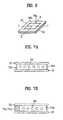
- FIG. 6is a perspective view illustrating an LCD device according to a fourth embodiment of the present invention.
- FIGS. 7A and 7Bare sectional views taken along lines I-I and II-II of FIG. 6 .
- FIGS. 3A to 3Dare perspective views illustrating a method of manufacturing an LCD device according to the first embodiment of the present invention.
- a lower substrate 10 and an upper substrate 30are prepared for the process.
- a plurality of gate and data linesare formed on the lower substrate 10 .
- the gate linescross the data lines to define a pixel region.
- a thin film transistor(not shown) having a gate electrode, a gate insulating layer, a semiconductor layer, an ohmic contact layer, source/drain electrodes, and a protection layer is formed at each crossing point of the gate lines and the data lines.
- a pixel electrode (not shown) connected with the thin film transistoris formed in the pixel region.
- the alignment filmis formed on the pixel electrode to initially align the molecules of liquid crystal.
- the alignment filmmay be formed of polyamide or polyimide based compound, polyvinylalcohol (PVA), and polyamic acid by rubbing.
- the alignment filmmay be formed of a photosensitive material, such as polyvinvylcinnamate (PVCN), polysilioxanecinnamate (PSCN) or cellulosecinnamate (CelCN) based compound, by using a photo-alignment method.
- a light-shielding layer(not shown) is formed on the upper substrate 30 to shield light leakage from the gate lines, the data lines, and the thin film transistor regions.
- a color filter layer(not shown) of R, G, and B is formed on the light-shielding layer.
- a common electrode(not shown) is formed on the color filter layer. Additionally, an overcoat layer (not shown) may be formed between the color filter layer and the common electrode. The alignment film is formed on the common electrode.
- Silver (Ag) dotsare formed outside the lower substrate 10 to apply a voltage to the common electrode on the upper substrate 30 after the lower and upper substrates 10 and 30 are attached to each other.
- the silver dotsmay be formed on the upper substrate 30 .
- the common electrodeis formed on the lower substrate like the pixel electrode, and so that an electric field can be horizontally induced between the common electrode and the pixel electrode.
- the silver dotsare not formed on the substrate.
- a liquid crystal 50is applied onto the lower substrate 10 to form a liquid crystal layer.
- An auxiliary UV curable sealant 70 ais formed in a dummy area at a corner region of the upper substrate 30 , subsequently, a main UV curable sealant 70 b having no injection hole is formed, using a dispensing method.
- the auxiliary UV sealant 70 ais prevents any problem that may occur due to a sealant concentrated upon the end of a nozzle of a dispensing device. Therefore, it does not matter where the auxiliary UV sealant 70 a is formed in the dummy area of the substrate, i.e., any blob of-sealant will be formed away from the active region of the liquid crystal display device and away from a region where the liquid crystal panel will be cut away from the mother substrate assembly. Formation of the main UV sealant 70 b is preceded by the formation of the auxiliary UV sealant 70 a.
- the auxiliary UV sealant 70 amay be formed in a straight line as shown. Alternatively, the auxiliary UV sealant 70 a may be formed in a curved line or other shape as long as it is formed in a dummy region.
- Monomers or oligomers each having both ends coupled to the acrylic group, mixed with an initiatorare used as the UV sealants 70 a and 70 b.
- monomers or oligomers each having one end coupled to the acrylic group and the other end coupled to the epoxy group, mixed with an initiatorare used as the UV sealants 70 a and 70 b.
- the liquid crystal 50may be contaminated if it comes into contact with the main UV sealant 70 b before the main UV sealant 70 b is hardened. Accordingly, the liquid crystal 50 may preferably be applied on the central part of the lower substrate 10 . In this case, the liquid crystal 50 is gradually spread even after the main UV sealant 70 b is hardened. Thus, the liquid crystal 50 is uniformly distributed on the substrate.
- the liquid crystal 50may be formed on the upper substrate 30 while the UV sealants 70 a and 70 b may be formed on the lower substrate 10 .
- the liquid crystal 50 and the UV sealants 70 a and 70 bmay be formed on one substrate.
- the substratemay not be cleaned even if the sealant contaminates the panel before the substrates are attached to each other.
- a cleaning process for cleaning the upper substrate 30may additionally be provided before the attaching process after the UV sealants 70 a and 70 b are formed on the upper substrate 30 .
- spacersmay be formed on either of the two substrates 10 and 30 to maintain a cell gap.
- the spacersmay be formed on the upper substrate 30 .
- Ball spacers or column spacersmay be used as the spacers.
- the ball spacersmay be formed in such a manner that they are mixed with a solution having an appropriate concentration and then spread at a high pressure onto the substrate from a spray nozzle.
- the column spacersmay be formed on portions of the substrate corresponding to the gate lines or data lines.
- column spacersmay be used for the large sized substrate since the ball spacers may cause an uneven cell gap for the large sized substrate.
- the column spacersmay be formed of a photosensitive organic resin.
- the lower substrate 10 and the upper substrate 30are attached to each other by the following processes.
- one of the substrates having the liquid crystal dropped thereonis placed at the lower side.
- the other substrateis placed at the upper side by turning by 180 degrees so that its portion having layers faces into the substrate at the lower side.
- the substrate at the upper sideis pressed, so that both substrates are attached to each other.
- the space between the substratesmay be maintained under the vacuum state so that both substrates are attached to each other by releasing the vacuum state.
- UV lightis irradiated upon the attached substrates through a UV irradiating device 90 .
- monomers or oligomers activated by an initiator constituting the UV sealantsare polymerized and hardened, thereby bonding the lower substrate 10 to the upper substrate 30 .
- the sealantsmay have to be additionally heated at about 120° C. for one hour after the UV irradiation, thereby hardening the sealants completely.
- the bonded substratesare cut into a unit cells and final test processes are performed.
- a scribing processis performed by forming a cutting line on surfaces of the substrates with a pen or wheel of a material having hardness greater than that of glass, such as diamond, and then the substrates are cut along the cutting line by mechanical impact (breaking process).
- the scribing process and the breaking processmay simultaneously be performed using a pen or wheel of a diamond or other hard material.
- the cutting line of the cutting processis formed between the start point of the auxiliary sealant, which may be a blob A of sealant, and a main UV sealant across the initially formed auxiliary UV sealant 70 a. Consequently, a substantial portion of the excessively distributed auxiliary UV sealant 70 a is removed.
- FIGS. 4A to 4Dare perspective views illustrating a process of irradiating UV light in the method of manufacturing an LCD device according to the second embodiment of the present invention.
- the second embodimentis similar to the first embodiment except for the UV irradiation process.
- a region where the sealants are not formedis covered with a mask before the UV light is irradiated. Since the other elements of the second embodiment are the same as those of the first embodiment, the same reference numerals will be given to the same elements and their detailed description will be omitted.
- the UV lightmay deteriorate characteristics of devices such as a thin film transistor on the substrate and may change a pre-tilt angle of an alignment film formed for the initial alignment of the liquid crystal.
- the UV lightis irradiated when the area where no sealant is formed is covered with a mask.
- a region where the auxiliary UV sealant 70 a and the main UV sealant 70 b are formedis covered with a mask 80 .
- the mask 80is placed at an upper side of the attached substrates, and the UV light is irradiated.
- the mask 80may be placed at a lower side of the attached substrates. Also, although the UV light is irradiated upon the upper substrate 30 of the attached substrates as shown, the UV light may be irradiated upon the lower substrate 10 by turning the attached substrates.
- UV light from a UV irradiating device 90is reflected and irradiated upon an opposite side, it may deteriorate characteristics of devices, such as the thin film transistor on the substrate and the alignment film, as described above. Therefore, masks are preferably formed at lower and upper sides of the attached substrates.
- masks 80 and 82 that cover the region where the sealants 70 a and 70 b are not formed are placedare at upper and lower sides of the attached substrates. The UV light is then irradiated thereupon.
- auxiliary UV sealant 70 adoes not act as a sealant, it does not require hardening. Also, since the region of the auxiliary UV sealant 70 a overlaps the cell cutting line during the later cell cutting process, it is more desirable for the cell cutting process that the auxiliary UV sealant 70 is not hardened.
- the auxiliary UV sealant 70 ais not hardened by irradiating the UV light when only the area where the main UV sealant 70 b is not formed is covered with the mask, i.e., the auxiliary sealant 70 a is also covered by a mask.
- the UV lightis irradiated with the mask 80 in place at a lower or upper side of the attached substrates.
- the UV lightis irradiated when the mask 80 is respectively placed at lower and upper sides of the attached substrates.
- FIGS. 5A and 5Bare perspective views illustrating a process of forming a UV sealant in a method of manufacturing an LCD device according to the third embodiment of the present invention of the present invention.
- the third embodimentis identical to the second embodiment except for the UV irradiation process.
- the UV lightis irradiated at a tilt angle. Since the other elements of the third embodiment are identical to those of the second embodiment, the same reference numerals will be given to the same elements and their detailed description will be omitted.
- the UV lightis irradiated at a tilt angle upon the substrate where the UV sealant is formed, so that the UV sealant is hardened even if the light-shielding layer or the metal line layer is formed between the UV irradiating surface and the sealant.
- the attached substratesare horizontally arranged and a UV irradiating device 90 is arranged at a tilt angle of ⁇ .
- the attached substratesmay be arranged at a tilt angle and the UV irradiating device 90 may horizontally be arranged.
- the UV lightmay be irradiated at a tilt angle when the area where the sealant is not formed is covered with the mask as shown in FIGS. 4A to 4D .
- FIG. 6is a perspective view illustrating an LCD device according to the fourth embodiment of the present invention
- FIGS. 7A and 7Bare sectional views taken along lines I-I and II-II of FIG. 6 .
- an LCD deviceincludes lower and upper substrates 10 and 30 , a UV sealant between the lower and upper substrates 10 and 30 , having an auxiliary UV sealant 70 a in a dummy area and a perimeter of main UV sealant 70 b connected to the auxiliary UV sealant 70 a, and a liquid crystal layer 50 between the lower and upper substrates 10 and 30 .
- a thin film transistor, a pixel electrode, and an alignment filmare formed on the lower substrate 10 .
- a black matrix layer (not shown), a color filter layer (not shown), a common electrode (not shown) and an alignment film (not shown)are formed on the upper substrate 30 .
- spacersare formed between the lower and upper substrates 10 and 30 to maintain a cell gap between the substrates.
- the LCD device and the method of manufacturing the same according to the present inventionhave the following advantages.
- the sealant concentrated upon the end of the nozzle of the dispensing deviceis formed in the dummy area on the substrate, the liquid crystal layer is not contaminated by the attaching process of the substrates and the cell cutting process is easily performed.
- the UV lightis irradiated upon the substrate when the mask is formed at the lower and/or upper side of the attached substrates, the UV light is irradiated upon only the region where the UV sealant is formed.
- the alignment film formed on the substrateis not damaged and the characteristics of the devices, such as the thin film transistor, are not deteriorated.
- the sealantcan be hardened even if the light-shielding layer or the metal line is formed on the sealant, thereby avoiding reducing adherence between the lower and upper substrates.
Landscapes
- Physics & Mathematics (AREA)
- Nonlinear Science (AREA)
- Mathematical Physics (AREA)
- Chemical & Material Sciences (AREA)
- Crystallography & Structural Chemistry (AREA)
- General Physics & Mathematics (AREA)
- Optics & Photonics (AREA)
- Liquid Crystal (AREA)
Abstract
Description
This application claims the benefit of the Korean Application No. P2002-8900 filed on Feb. 20, 2002, which is hereby incorporated by reference for all purposes as if fully set forth herein.
This application incorporates by reference two applications, Ser. No. 10/184,096, filed on Jun. 28, 2002, entitled “SYSTEM AND METHOD FOR MANUFACTURING LIQUID CRYSTAL DISPLAY DEVICES”and Ser. No. 10/184,088, filed on Jun. 28, 2002, entitled “SYSTEM FOR FABRICATING LIQUID CRYSTAL DISPLAY AND METHOD OF FABRICATING LIQUID CRYSTAL DISPLAY USING THE SAME”, as if fully set forth herein.
1. Field of the Invention
The present invention relates to a liquid crystal display (LCD) device, and more particularly, to a sealant pattern of an LCD device manufactured by applying a liquid crystal to the surface of a substrate.
2. Discussion of the Related Art
Generally, ultra thin flat panel displays have a display screen with a thickness of several centimeters or less. In particular, flat panel LCD devices are widely used in monitors for notebook computers, spacecraft, and aircraft because such LCD devices have low power consumption and are easy to carry.
Such an LCD device includes a lower substrate, an upper substrate, and a liquid crystal layer. A thin film transistor (TFT) and a pixel electrode are formed on the lower substrate. The upper substrate is formed to oppose the lower substrate. A light-shielding layer, a color filter layer, and a common electrode are formed on the upper substrate. The liquid crystal layer is formed between the lower and upper substrates. In operation an electric field is formed between the lower and upper substrates by the pixel electrode and the common electrode so that the electric field “drives” the alignment of molecules in the liquid crystal layer. Light transmittivity is controlled by driving the liquid crystal layer so that a picture image is displayed.
In the aforementioned LCD device, to form the liquid crystal layer between lower and upper substrates, a vacuum injection method based on capillary phenomenon and pressure difference has been conventionally used. However, such a vacuum injection method has a problem in that it takes long time to inject the liquid crystal into a large display panel, thereby reducing manufacturing productivity.
To solve such a problem, a method of applying liquid crystal on the substrate has been developed and is generally described with reference toFIGS. 1A to 1D . Although the drawings illustrate only one unit cell, a plurality of unit cells may be formed depending upon the size of the substrate.
As shown inFIG. 1A , alower substrate 1 and anupper substrate 3 are prepared. A plurality of gate and data lines (not shown) are formed on thelower substrate 1. The gate lines cross the data lines to define a pixel region. A thin film transistor (not shown) is formed at each crossing point between the gate and data lines. A pixel electrode (not shown) connected with the thin film transistor is formed in the pixel region.
A light-shielding layer (not shown) is formed on theupper substrate 3 to prevent light from leaking out from the gate and data lines and the thin film transistor. Color filter layers of red(R), green(G), and blue(B) are formed on the light-shielding layer, and a common electrode is formed on the color filter layers. An alignment film (not shown) is formed on at least one of thelower substrate 1 and theupper substrate 3 to initially align the liquid crystal molecules.
As shown inFIG. 1B , asealant 7 is formed on thelower substrate 1 and a liquid crystal5 is applied thereon, so that a liquid crystal layer is formed. A spacer (not shown) is spread or sprayed onto theupper substrate 3 to maintain a cell gap between the upper and lower substrates.
In the method of manufacturing the LCD device based on the liquid crystal application method, a liquid crystal layer is formed on attached substrates before thesealant 7 is hardened. Therefore, if a thermo-hardening sealant is used as thesealant 7, the liquid crystal heats and expands so that it flows out of the substrate when it is heated. For this reason, a problem arises in that the liquid crystal5 is contaminated. Therefore, in the method of manufacturing the LCD based on the liquid crystal application method, a sealant that is at least partially curable by ultraviolet (UV) light is used as thesealant 7.
The UV sealant is formed by a screen printing method or a dispensing method. In the screen printing method, since a screen comes into contact with the substrate, the alignment film formed on the substrate may be damaged. Also, if the substrate has a large sized area, loss of the sealant increases. In these respects, the dispensing method is preferably used.
As shown inFIG. 1C , thelower substrate 1 is attached to theupper substrate 3.
As shown inFIG. 1D , UV light is irradiated through a UV irradiating device9 so that thesealant 7 is hardened.
Thereafter, although not shown, a cell cutting process and a final test process are performed, thereby completing a liquid crystal cell.
Meanwhile,FIGS. 2A and 2B are perspective views illustrating a process of forming a UV sealant using a dispensing method. In the method of applying liquid crystal to one of the substrates before attaching the the substrates, since no liquid crystal injection hole is required, asealant 7 having no injection hole is formed on alower substrate 1 using adispensing device 8.
However, since thesealant 7 has high viscosity, it is concentrated upon the end of a nozzle of the dispensingdevice 8 before thesealant 7 is dispensed. For this reason, a blob “A” of thesealant 7 is excessively deposited at the point where deposition of thesealant 7 on the substrate is started.
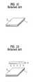
As shown inFIG. 2C , the excessively distributed sealant spreads into an active region (central part of the substrate) and a dummy region (outer part of the substrate) when thelower substrate 1 is attached to theupper substrate 3. In this case, a problem arises in that the sealant spreads into the active region and contaminates the liquid crystal while the sealant spread out to the dummy region makes the cell cutting process difficult, especially after the sealant is cured.
Accordingly, the present invention is directed to an LCD device and a method of manufacturing the same that substantially obviates one or more problems due to limitations and disadvantages of the related art.
An advantage of the present invention is to provide an LCD device and a method of manufacturing the same in which a sealant is formed so that a liquid crystal is not contaminated when both substrates are attached to each other and so that a cell cutting process can be easily performed.
Additional advantages and features of the invention will be set forth in part in the description which follows and in part will become apparent to those having ordinary skill in the art upon examination of the following or may be learned from practice of the invention. These and other advantages of the invention may be realized and attained by the structure particularly pointed out in the written description and claims hereof as well as the appended drawings.
To achieve these and other advantages and in accordance with the purpose of the invention, as embodied and broadly described herein, a method of manufacturing an LCD device according to the present invention includes preparing a lower substrate and an upper substrate; forming an auxiliary sealant and subsequently forming a main sealant on one of the lower and upper substrates, wherein the auxiliary sealant is formed in a dummy region and connect to the main sealant; applying a liquid crystal on one of the lower and upper substrates; attaching the lower and upper substrates; and curing at least the main sealant.
In one embodiment of the present invention, the supplementary UV sealant does not perform the ordinary the function of a sealant, that is, it does not prevent the liquid crystal from leaking out. While the main UV sealant acts as a sealant to confine the liquid crystal.
In another aspect of the present invention, a method of manufacturing a liquid crystal display (LCD) device includes preparing a lower substrate and an upper substrate; forming an auxiliary UV sealant and a main UV sealant on one of the lower and upper substrates, wherein the auxiliary UV sealant is formed in a dummy region and extends from the main UV sealant; applying a liquid crystal on one of the lower and upper substrates; attaching the lower and upper substrates; and irradiating UV light on the attached substrates.
In one aspect of the present invention, the supplementary UV sealant is formed in a dummy region on the substrate and then the closed type main UV sealant is formed, so that the sealant concentrated upon the end of a nozzle of a dispensing device is formed in the dummy region on the substrate.
It is to be understood that both the foregoing general description and the following detailed description of the present invention are exemplary and explanatory and are intended to provide further explanation of the invention as claimed.
The accompanying drawings, which are included to provide a further understanding of the invention and are incorporated in and constitute a part of this application, illustrate embodiment(s) of the invention and together with the description serve to explain the principle of the invention.
In the drawings:
Reference will now be made in detail to the illustrated embodiments of the present invention, examples of which are illustrated in the accompanying drawings. Wherever possible, the same reference numbers will be used throughout the drawings to refer to the same or like parts.
Although the drawings illustrate only one unit cell, a plurality of unit cells may be formed depending upon the size of the substrate.
As shown inFIG. 3A , alower substrate 10 and anupper substrate 30 are prepared for the process. A plurality of gate and data lines (not shown) are formed on thelower substrate 10. The gate lines cross the data lines to define a pixel region. A thin film transistor (not shown) having a gate electrode, a gate insulating layer, a semiconductor layer, an ohmic contact layer, source/drain electrodes, and a protection layer is formed at each crossing point of the gate lines and the data lines. A pixel electrode (not shown) connected with the thin film transistor is formed in the pixel region.
An alignment film (not shown) is formed on the pixel electrode to initially align the molecules of liquid crystal. The alignment film may be formed of polyamide or polyimide based compound, polyvinylalcohol (PVA), and polyamic acid by rubbing. Alternatively, the alignment film may be formed of a photosensitive material, such as polyvinvylcinnamate (PVCN), polysilioxanecinnamate (PSCN) or cellulosecinnamate (CelCN) based compound, by using a photo-alignment method.
A light-shielding layer (not shown) is formed on theupper substrate 30 to shield light leakage from the gate lines, the data lines, and the thin film transistor regions. A color filter layer (not shown) of R, G, and B is formed on the light-shielding layer. A common electrode (not shown) is formed on the color filter layer. Additionally, an overcoat layer (not shown) may be formed between the color filter layer and the common electrode. The alignment film is formed on the common electrode.
Silver (Ag) dots are formed outside thelower substrate 10 to apply a voltage to the common electrode on theupper substrate 30 after the lower andupper substrates upper substrate 30.
For an in plane switching (IPS) mode LCD, the common electrode is formed on the lower substrate like the pixel electrode, and so that an electric field can be horizontally induced between the common electrode and the pixel electrode. The silver dots are not formed on the substrate.
As shown inFIG. 3B , aliquid crystal 50 is applied onto thelower substrate 10 to form a liquid crystal layer.
An auxiliary UVcurable sealant 70a is formed in a dummy area at a corner region of theupper substrate 30, subsequently, a main UVcurable sealant 70b having no injection hole is formed, using a dispensing method.
Theauxiliary UV sealant 70a is prevents any problem that may occur due to a sealant concentrated upon the end of a nozzle of a dispensing device. Therefore, it does not matter where theauxiliary UV sealant 70a is formed in the dummy area of the substrate, i.e., any blob of-sealant will be formed away from the active region of the liquid crystal display device and away from a region where the liquid crystal panel will be cut away from the mother substrate assembly. Formation of themain UV sealant 70b is preceded by the formation of theauxiliary UV sealant 70a. Theauxiliary UV sealant 70a may be formed in a straight line as shown. Alternatively, theauxiliary UV sealant 70a may be formed in a curved line or other shape as long as it is formed in a dummy region.
Monomers or oligomers each having both ends coupled to the acrylic group, mixed with an initiator are used as theUV sealants UV sealants
Also, theliquid crystal 50 may be contaminated if it comes into contact with themain UV sealant 70b before themain UV sealant 70b is hardened. Accordingly, theliquid crystal 50 may preferably be applied on the central part of thelower substrate 10. In this case, theliquid crystal 50 is gradually spread even after themain UV sealant 70b is hardened. Thus, theliquid crystal 50 is uniformly distributed on the substrate.
Theliquid crystal 50 may be formed on theupper substrate 30 while theUV sealants lower substrate 10. Alternatively, theliquid crystal 50 and theUV sealants
Accordingly, a cleaning process for cleaning theupper substrate 30 may additionally be provided before the attaching process after theUV sealants upper substrate 30.
Meanwhile, spacers may be formed on either of the twosubstrates upper substrate 30.
Ball spacers or column spacers may be used as the spacers. The ball spacers may be formed in such a manner that they are mixed with a solution having an appropriate concentration and then spread at a high pressure onto the substrate from a spray nozzle. The column spacers may be formed on portions of the substrate corresponding to the gate lines or data lines. Preferably, column spacers may be used for the large sized substrate since the ball spacers may cause an uneven cell gap for the large sized substrate. The column spacers may be formed of a photosensitive organic resin.
As shown inFIG. 3C , thelower substrate 10 and theupper substrate 30 are attached to each other by the following processes. First, one of the substrates having the liquid crystal dropped thereon is placed at the lower side. The other substrate is placed at the upper side by turning by 180 degrees so that its portion having layers faces into the substrate at the lower side. Thereafter, the substrate at the upper side is pressed, so that both substrates are attached to each other. Alternatively, the space between the substrates may be maintained under the vacuum state so that both substrates are attached to each other by releasing the vacuum state.
Then, as shown inFIG. 3D , UV light is irradiated upon the attached substrates through aUV irradiating device 90.
Upon irradiating the UV light, monomers or oligomers activated by an initiator constituting the UV sealants are polymerized and hardened, thereby bonding thelower substrate 10 to theupper substrate 30.
If monomers or oligomers each having one end coupled to the acrylic group and the other end coupled to the epoxy group, mixed with an initiator are used as the UV sealants, the epoxy group is not completely polymerized by the application of UV light. Therefore, the sealants may have to be additionally heated at about 120° C. for one hour after the UV irradiation, thereby hardening the sealants completely.
Afterwards, although not shown, the bonded substrates are cut into a unit cells and final test processes are performed.
In the cutting process, a scribing process is performed by forming a cutting line on surfaces of the substrates with a pen or wheel of a material having hardness greater than that of glass, such as diamond, and then the substrates are cut along the cutting line by mechanical impact (breaking process). Alternatively, the scribing process and the breaking process may simultaneously be performed using a pen or wheel of a diamond or other hard material.
The cutting line of the cutting process is formed between the start point of the auxiliary sealant, which may be a blob A of sealant, and a main UV sealant across the initially formedauxiliary UV sealant 70a. Consequently, a substantial portion of the excessively distributedauxiliary UV sealant 70a is removed.
If the UV light is irradiated upon the entire surface of the attached substrates, the UV light may deteriorate characteristics of devices such as a thin film transistor on the substrate and may change a pre-tilt angle of an alignment film formed for the initial alignment of the liquid crystal.
Therefore, in the second embodiment of the present invention, the UV light is irradiated when the area where no sealant is formed is covered with a mask.
Referring toFIG. 4A , a region where theauxiliary UV sealant 70a and themain UV sealant 70b are formed is covered with amask 80. Themask 80 is placed at an upper side of the attached substrates, and the UV light is irradiated.
Also, themask 80 may be placed at a lower side of the attached substrates. Also, although the UV light is irradiated upon theupper substrate 30 of the attached substrates as shown, the UV light may be irradiated upon thelower substrate 10 by turning the attached substrates.
If the UV light from aUV irradiating device 90 is reflected and irradiated upon an opposite side, it may deteriorate characteristics of devices, such as the thin film transistor on the substrate and the alignment film, as described above. Therefore, masks are preferably formed at lower and upper sides of the attached substrates.
That is, as shown inFIG. 4B , masks80 and82 that cover the region where thesealants
Meanwhile, since theauxiliary UV sealant 70a does not act as a sealant, it does not require hardening. Also, since the region of theauxiliary UV sealant 70a overlaps the cell cutting line during the later cell cutting process, it is more desirable for the cell cutting process that the auxiliary UV sealant70 is not hardened.
Referring toFIGS. 4C and 4D , theauxiliary UV sealant 70a is not hardened by irradiating the UV light when only the area where themain UV sealant 70b is not formed is covered with the mask, i.e., theauxiliary sealant 70a is also covered by a mask.
In this case, inFIG. 4C , the UV light is irradiated with themask 80 in place at a lower or upper side of the attached substrates. InFIG. 4D , the UV light is irradiated when themask 80 is respectively placed at lower and upper sides of the attached substrates.
The third embodiment is identical to the second embodiment except for the UV irradiation process. In the third embodiment, the UV light is irradiated at a tilt angle. Since the other elements of the third embodiment are identical to those of the second embodiment, the same reference numerals will be given to the same elements and their detailed description will be omitted.
If a light-shielding layer and a metal line such as gate and data lines are formed on a region where the UV sealant is formed, the UV light is not irradiated upon the region, thereby failing to harden the sealant. For this reason, adherence between the lower and upper substrates is reduced.
Therefore, in the third embodiment of the present invention, the UV light is irradiated at a tilt angle upon the substrate where the UV sealant is formed, so that the UV sealant is hardened even if the light-shielding layer or the metal line layer is formed between the UV irradiating surface and the sealant.
To irradiate the UV light at a tilt angle, as shown inFIG. 5A , the attached substrates are horizontally arranged and aUV irradiating device 90 is arranged at a tilt angle of θ. Alternatively, as shown inFIG. 5B , the attached substrates may be arranged at a tilt angle and theUV irradiating device 90 may horizontally be arranged.
Also, the UV light may be irradiated at a tilt angle when the area where the sealant is not formed is covered with the mask as shown inFIGS. 4A to 4D .
As shown inFIGS. 6 and 7 , an LCD device according to the present invention includes lower andupper substrates upper substrates auxiliary UV sealant 70a in a dummy area and a perimeter ofmain UV sealant 70b connected to theauxiliary UV sealant 70a, and aliquid crystal layer 50 between the lower andupper substrates
At this time, although not shown, a thin film transistor, a pixel electrode, and an alignment film are formed on thelower substrate 10. A black matrix layer (not shown), a color filter layer (not shown), a common electrode (not shown) and an alignment film (not shown) are formed on theupper substrate 30. Also, spacers are formed between the lower andupper substrates
As aforementioned, the LCD device and the method of manufacturing the same according to the present invention have the following advantages.
Since the sealant concentrated upon the end of the nozzle of the dispensing device is formed in the dummy area on the substrate, the liquid crystal layer is not contaminated by the attaching process of the substrates and the cell cutting process is easily performed.
Furthermore, if the UV light is irradiated upon the substrate when the mask is formed at the lower and/or upper side of the attached substrates, the UV light is irradiated upon only the region where the UV sealant is formed. In this case, the alignment film formed on the substrate is not damaged and the characteristics of the devices, such as the thin film transistor, are not deteriorated.
Finally, if the UV light is irradiated at a tilt angle, the sealant can be hardened even if the light-shielding layer or the metal line is formed on the sealant, thereby avoiding reducing adherence between the lower and upper substrates.
It will be apparent to those skilled in the art that various modifications and variations can be made in the present invention. Thus, it is intended that the present invention covers the modifications and variations of this invention provided they come within the scope of the appended claims and their equivalents.
Claims (38)
1. A method of manufacturing a liquid crystal display (LCD) device comprising:
preparing a lower substrate and an upper substrate;
forming an auxiliary sealant and subsequently forming a main sealant on one of the lower and upper substrates, wherein the auxiliary sealant is formed in a dummy region and connects to the main sealant, and wherein the auxiliary sealant and the main sealant are contiguous;
applying a liquid crystal on one of the lower and upper substrates;
attaching the lower and upper substrates; and
curing at least the main sealant.
2. The method ofclaim 1 , wherein the main sealant and the auxiliary sealant are at least partially curable by irradiating UV light and curing the main sealant includes irradiating UV light.
3. The method of claim2 31, wherein curing the main sealant includes irradiating UV light, and the sealant is formed using oligomers each having both ends coupled to an acrylic group.
4. The method of claim2 31, wherein curing the main sealant includes irradiating UV light, and the sealant is formed using monomers each having both ends coupled to an acrylic group.
5. The method ofclaim 2 , wherein the sealant is formed using oligomers each having one end coupled to an acrylic group and the other end coupled to an epoxy group.
6. The method ofclaim 5 , further comprising heating the sealant after irradiating the UV light.
7. The method of claim2 31, wherein curing the main sealant includes irradiating UV light, and the sealant is formed using monomers each having one end coupled to an acrylic group and the other end coupled to an epoxy group.
8. The method ofclaim 7 , further comprising heating the sealant after irradiating the UV light.
9. The method ofclaim 2 , further comprising heating the sealant after irradiating the UV light.
10. The method of claim2 31, wherein curing the main sealant includes irradiating UV light, and a region where the sealant is not formed is covered with a mask during the irradiating with UV light.
11. The method ofclaim 2 , wherein a region where the main UV sealant is not formed is covered with a mask during the irradiating with UV light.
12. The method of claim2 31, wherein curing the main sealant includes irradiating UV light, and the UV light is irradiated at a tilt angle with respect to the attached substrates.
13. The method of claim2 31, wherein curing the main sealant includes irradiating UV light, the method further comprising:
providing a mask over a region where the main sealant is not formed before irradiating UV light such that the auxiliary sealant is not exposed to the UV light; and
cutting the attached substrates.
14. The method of claim1 31, further comprising forming column spacers on the upper substrate.
15. The method of claim1 31, wherein the main and auxiliary sealants are formed on the upper substrate and the liquid crystal is applied to the lower substrate.
16. The method ofclaim 1 , further comprising cutting the attached substrates.
17. The method ofclaim 16 , wherein the attached substrates are cut across a portion of the auxiliary sealant.
18. The method of claim1 31, wherein the applying the liquid crystal includes dropping the liquid crystal onto the one of the upper and lower substrates.
19. The method ofclaim 18 , wherein the liquid crystal is applied in a predetermined pattern onto the one of the upper and lower substrates.
20. The method ofclaim 1 , wherein the auxiliary sealant contacts the main sealant.
21. A method of manufacturing a liquid crystal display (LCD) device comprising:
preparing a lower substrate and an upper substrate;
forming an auxiliary UV sealant and a main UV sealant on one of the lower and upper substrates, wherein the auxiliary UV sealant is formed in a dummy region and extends outside from the main UV sealant, wherein the auxiliary UV sealant contacts the main UV sealant;
applying a liquid crystal on one of the lower and upper substrates;
attaching the lower and upper substrates; and
irradiating UV light on the attached substrates.
22. The method of claim21 23, wherein the UV light is irradiated at a tilt angle with respect to the attached substrates.
23. A method of manufacturing a liquid crystal display (LCD) device comprising:
preparing a lower substrate and an upper substrate;
forming an auxiliary UV sealant and a main UV sealant on one of the lower and upper substrates, wherein:
the main UV sealant has no injection hole;
the auxiliary UV sealant is formed in a dummy region and extends outside from the main UV sealant;
the auxiliary UV sealant includes a sealant blob at a sealant deposition starting point; and
the auxiliary UV sealant contacts the main UV sealant;
applying a liquid crystal on one of the lower and upper substrates;
attaching the lower and upper substrates; and
irradiating UV light on the attached substrates.
24. The method of claim 23, wherein the sealant blob is deposited completely outside of an area enclosed by the main UV sealant.
25. The method of claim 23, wherein the auxiliary UV sealant contacts the main UV sealant at a substantially 90-degree angle.
26. The method of claim 23, wherein the auxiliary UV sealant forms a substantially straight line between the sealant blob and the main UV sealant.
27. The method of claim 23, wherein the auxiliary UV sealant forms a curve between the sealant blob and the main UV sealant.
28. The method of claim 23, further comprising cutting the attached substrates across a portion of the auxiliary UV sealant between the sealant blob and the main UV sealant.
29. The method of claim 23, wherein the main UV sealant defines a completely enclosed active region on one of the lower and upper substrates.
30. The method of claim 23, wherein the auxiliary UV sealant is not connected to an injection hole.
31. A method of manufacturing a liquid crystal display (LCD) device comprising:
preparing a lower substrate and an upper substrate;
forming an auxiliary sealant that is at least partially curable by ultraviolet light and subsequently forming a main sealant that is at least partially curable by ultraviolet light on one of the lower and upper substrates, wherein:
the main sealant has no injection hole;
the auxiliary sealant is formed in a dummy region and connects to the main sealant;
the auxiliary sealant includes a sealant blob at a sealant deposition starting point; and
the auxiliary sealant and the main sealant are contiguous;
applying a liquid crystal on one of the lower and upper substrates;
attaching the lower and upper substrates; and
curing at least the main sealant.
32. The method of claim 31, wherein the sealant blob is deposited completely outside of an area enclosed by the main sealant.
33. The method of claim 31, wherein the auxiliary sealant connects to the main sealant at a substantially 90-degree angle.
34. The method of claim 31, wherein the auxiliary sealant forms a substantially straight line between the sealant blob and the main sealant.
35. The method of claim 31, wherein the auxiliary sealant forms a curve between the sealant blob and the main sealant.
36. The method of claim 31, further comprising cutting the attached substrates across a portion of the auxiliary sealant between the sealant blob and the main sealant.
37. The method of claim 31, wherein the main sealant defines a completely enclosed active region on one of the lower and upper substrates.
38. The method of claim 31, wherein the auxiliary sealant is not connected to an injection hole.
Priority Applications (1)
| Application Number | Priority Date | Filing Date | Title |
|---|---|---|---|
| US13/960,713USRE46146E1 (en) | 2002-02-20 | 2013-08-06 | Liquid crystal display device and method of manufacturing the same |
Applications Claiming Priority (5)
| Application Number | Priority Date | Filing Date | Title |
|---|---|---|---|
| KR0208900 | 2002-02-20 | ||
| KR1020020008900AKR100672641B1 (en) | 2002-02-20 | 2002-02-20 | LCD and its manufacturing method |
| KR2002-8900 | 2002-02-20 | ||
| US10/184,118US7218374B2 (en) | 2002-02-20 | 2002-06-28 | Liquid crystal display device and method of manufacturing the same |
| US13/960,713USRE46146E1 (en) | 2002-02-20 | 2013-08-06 | Liquid crystal display device and method of manufacturing the same |
Related Parent Applications (1)
| Application Number | Title | Priority Date | Filing Date |
|---|---|---|---|
| US10/184,118ReissueUS7218374B2 (en) | 2002-02-20 | 2002-06-28 | Liquid crystal display device and method of manufacturing the same |
Publications (1)
| Publication Number | Publication Date |
|---|---|
| USRE46146E1true USRE46146E1 (en) | 2016-09-13 |
Family
ID=27725786
Family Applications (2)
| Application Number | Title | Priority Date | Filing Date |
|---|---|---|---|
| US10/184,118CeasedUS7218374B2 (en) | 2002-02-20 | 2002-06-28 | Liquid crystal display device and method of manufacturing the same |
| US13/960,713Expired - LifetimeUSRE46146E1 (en) | 2002-02-20 | 2013-08-06 | Liquid crystal display device and method of manufacturing the same |
Family Applications Before (1)
| Application Number | Title | Priority Date | Filing Date |
|---|---|---|---|
| US10/184,118CeasedUS7218374B2 (en) | 2002-02-20 | 2002-06-28 | Liquid crystal display device and method of manufacturing the same |
Country Status (4)
| Country | Link |
|---|---|
| US (2) | US7218374B2 (en) |
| JP (2) | JP2003241204A (en) |
| KR (1) | KR100672641B1 (en) |
| CN (1) | CN1223882C (en) |
Families Citing this family (15)
| Publication number | Priority date | Publication date | Assignee | Title |
|---|---|---|---|---|
| KR100755645B1 (en)* | 2000-12-29 | 2007-09-04 | 엘지.필립스 엘시디 주식회사 | LCD and its manufacturing method |
| KR100672641B1 (en)* | 2002-02-20 | 2007-01-23 | 엘지.필립스 엘시디 주식회사 | LCD and its manufacturing method |
| US7102726B2 (en)* | 2002-03-15 | 2006-09-05 | Lg. Philips Lcd Co., Ltd. | System for fabricating liquid crystal display and method of fabricating liquid crystal display using the same |
| TW594303B (en)* | 2003-11-03 | 2004-06-21 | Chi Mei Optoelectronics Corp | Liquid crystal display cell and method for manufacturing the same |
| KR100689313B1 (en)* | 2003-11-22 | 2007-03-08 | 엘지.필립스 엘시디 주식회사 | Silver-Silent Hybrid Dispenser and Dispensing Method of Liquid Crystal Display Panel Using Same Dispenser |
| KR100710683B1 (en)* | 2004-05-12 | 2007-04-24 | 주식회사 탑 엔지니어링 | Sealant Dispenser |
| KR101018650B1 (en)* | 2004-05-31 | 2011-03-03 | 엘지디스플레이 주식회사 | Seal application system and method of forming seal pattern using the same |
| JP4389780B2 (en) | 2004-12-27 | 2009-12-24 | セイコーエプソン株式会社 | Method for manufacturing liquid crystal device, liquid crystal device, and electronic apparatus |
| JP4196944B2 (en) | 2004-12-27 | 2008-12-17 | セイコーエプソン株式会社 | Manufacturing method of liquid crystal device |
| JP2006215235A (en)* | 2005-02-03 | 2006-08-17 | Sony Corp | Method for manufacturing liquid crystal element, liquid crystal element, liquid crystal display device, and projection device |
| JP5125417B2 (en)* | 2007-10-31 | 2013-01-23 | カシオ計算機株式会社 | Protection plate integrated display panel |
| JP2009169152A (en)* | 2008-01-17 | 2009-07-30 | Ips Alpha Technology Ltd | Liquid crystal display device |
| US20120006466A1 (en) | 2008-12-31 | 2012-01-12 | Lensvector Inc. | Method of manufacturing a liquid crystal device |
| CN104614948B (en)* | 2015-02-02 | 2018-01-23 | 京东方科技集团股份有限公司 | A kind of ultraviolet curing mask plate and preparation method thereof and display device |
| WO2016190229A1 (en)* | 2015-05-28 | 2016-12-01 | シャープ株式会社 | Display panel production management system and display panel production management method |
Citations (245)
| Publication number | Priority date | Publication date | Assignee | Title |
|---|---|---|---|---|
| JPS5165656A (en) | 1974-12-04 | 1976-06-07 | Shinshu Seiki Kk | |
| US3978580A (en) | 1973-06-28 | 1976-09-07 | Hughes Aircraft Company | Method of fabricating a liquid crystal display |
| US4094058A (en) | 1976-07-23 | 1978-06-13 | Omron Tateisi Electronics Co. | Method of manufacture of liquid crystal displays |
| JPS5738414A (en) | 1980-08-20 | 1982-03-03 | Showa Denko Kk | Spacer for display panel |
| JPS5788428A (en) | 1980-11-20 | 1982-06-02 | Ricoh Elemex Corp | Manufacture of liquid crystal display body device |
| JPS5827126A (en) | 1981-08-11 | 1983-02-17 | Nec Corp | Production of liquid crystal display panel |
| JPS5957221A (en) | 1982-09-28 | 1984-04-02 | Asahi Glass Co Ltd | Production of display element |
| JPS59195222A (en) | 1983-04-19 | 1984-11-06 | Matsushita Electric Ind Co Ltd | Manufacture of liquid-crystal panel |
| JPS60111221A (en) | 1983-11-19 | 1985-06-17 | Nippon Denso Co Ltd | Method and device for charging liquid crystal |
| JPS60164723A (en) | 1984-02-07 | 1985-08-27 | Seiko Instr & Electronics Ltd | Liquid crystal display device |
| JPS60217343A (en) | 1984-04-13 | 1985-10-30 | Matsushita Electric Ind Co Ltd | Liquid crystal display device and its preparation |
| JPS617822A (en) | 1984-06-22 | 1986-01-14 | Canon Inc | Production of liquid crystal element |
| JPS6155625A (en) | 1984-08-24 | 1986-03-20 | Nippon Denso Co Ltd | Manufacture of liquid crystal element |
| JPS6254225A (en) | 1985-07-15 | 1987-03-09 | Semiconductor Energy Lab Co Ltd | Manufacturing method for liquid crystal display |
| JPS6254228A (en) | 1985-07-15 | 1987-03-09 | Semiconductor Energy Lab Co Ltd | Manufacturing method for liquid crystal display |
| US4653864A (en) | 1986-02-26 | 1987-03-31 | Ovonic Imaging Systems, Inc. | Liquid crystal matrix display having improved spacers and method of making same |
| JPS6289025A (en) | 1985-10-15 | 1987-04-23 | Matsushita Electric Ind Co Ltd | Manufacturing method of liquid crystal display panel |
| JPS6290622A (en) | 1985-10-17 | 1987-04-25 | Seiko Epson Corp | liquid crystal display device |
| US4691995A (en) | 1985-07-15 | 1987-09-08 | Semiconductor Energy Laboratory Co., Ltd. | Liquid crystal filling device |
| JPS62205319A (en) | 1986-03-06 | 1987-09-09 | Canon Inc | Ferroelectric liquid crystal element |
| JPS63110425A (en) | 1986-10-29 | 1988-05-14 | Toppan Printing Co Ltd | Cell for liquid crystal filling |
| JPS63109413A (en) | 1986-10-27 | 1988-05-14 | Fujitsu Ltd | Manufacturing method of LCD display |
| JPS63128315A (en) | 1986-11-19 | 1988-05-31 | Victor Co Of Japan Ltd | Liquid crystal display element |
| US4775225A (en) | 1985-05-16 | 1988-10-04 | Canon Kabushiki Kaisha | Liquid crystal device having pillar spacers with small base periphery width in direction perpendicular to orientation treatment |
| JPS63311233A (en) | 1987-06-12 | 1988-12-20 | Toyota Motor Corp | lcd cell |
| JPH039549A (en) | 1989-05-16 | 1991-01-17 | Motorola Inc | Composite integrated storage device |
| US5089358A (en)* | 1988-11-05 | 1992-02-18 | Brother Kogyo Kabushiki Kaisha | Optical recording medium |
| JPH0536425A (en) | 1991-02-12 | 1993-02-12 | Tokyo Electric Power Co Inc:The | Alloy separator for solid oxide fuel cell and method for producing the same |
| JPH0536426A (en) | 1991-07-31 | 1993-02-12 | Mitsubishi Heavy Ind Ltd | Solid electrolytic fuel cell |
| JPH05107533A (en) | 1991-10-16 | 1993-04-30 | Shinetsu Eng Kk | Method for laminating glass substrate for liquid crystal display panel and laminating apparatus therefor |
| JPH05127179A (en) | 1991-11-01 | 1993-05-25 | Ricoh Co Ltd | Production of liquid crystal display element |
| JPH05154923A (en) | 1991-12-06 | 1993-06-22 | Hitachi Ltd | Substrate assembling device |
| US5247377A (en) | 1988-07-23 | 1993-09-21 | Rohm Gmbh Chemische Fabrik | Process for producing anisotropic liquid crystal layers on a substrate |
| JPH05265011A (en) | 1992-03-19 | 1993-10-15 | Seiko Instr Inc | Production of liquid crystal display element |
| JPH05281557A (en) | 1992-04-01 | 1993-10-29 | Matsushita Electric Ind Co Ltd | Liquid crystal panel manufacturing method |
| JPH05281562A (en) | 1992-04-01 | 1993-10-29 | Matsushita Electric Ind Co Ltd | Manufacture of liquid crystal panel |
| US5263888A (en) | 1992-02-20 | 1993-11-23 | Matsushita Electric Industrial Co., Ltd. | Method of manufacture of liquid crystal display panel |
| JPH0618829A (en) | 1992-06-30 | 1994-01-28 | Shinetsu Eng Kk | Device for laminating glass substrates for liquid crystal display boards |
| JPH0651256A (en) | 1992-07-30 | 1994-02-25 | Matsushita Electric Ind Co Ltd | Device for discharging liquid crystal |
| JPH0664229A (en) | 1992-08-24 | 1994-03-08 | Toshiba Corp | Optical printing head |
| US5307190A (en)* | 1991-08-19 | 1994-04-26 | Matsushita Electric Industrial Co., Ltd. | Ferroelectric liquid crystal panel and method of manufacturing same |
| JPH06148657A (en) | 1992-11-06 | 1994-05-27 | Matsushita Electric Ind Co Ltd | Method of manufacturing cell for liquid crystal display and manufacturing apparatus thereof |
| JPH06160871A (en) | 1992-11-26 | 1994-06-07 | Matsushita Electric Ind Co Ltd | Liquid crystal display panel and manufacturing method thereof |
| JPH06194637A (en) | 1992-12-24 | 1994-07-15 | Shinetsu Eng Kk | Method for sticking glass substrate for liquid crystal display plate |
| JPH06235925A (en) | 1993-02-10 | 1994-08-23 | Matsushita Electric Ind Co Ltd | Manufacture of liquid crystal display element |
| JPH06265915A (en) | 1993-03-12 | 1994-09-22 | Matsushita Electric Ind Co Ltd | Discharge device for filling liquid crystal |
| JPH06313870A (en) | 1993-04-28 | 1994-11-08 | Hitachi Ltd | Substrate assembly device |
| US5379139A (en) | 1986-08-20 | 1995-01-03 | Semiconductor Energy Laboratory Co., Ltd. | Liquid crystal device and method for manufacturing same with spacers formed by photolithography |
| JPH0784268A (en) | 1993-09-13 | 1995-03-31 | Hitachi Ltd | Sealing agent drawing method |
| US5406989A (en) | 1993-10-12 | 1995-04-18 | Ayumi Industry Co., Ltd. | Method and dispenser for filling liquid crystal into LCD cell |
| US5410423A (en)* | 1992-02-21 | 1995-04-25 | Canon Kabushiki Kaisha | Method of fabricating a liquid crystal panel using a dummy seal which is closed after hardening |
| JPH07128674A (en) | 1993-11-05 | 1995-05-19 | Matsushita Electric Ind Co Ltd | Liquid crystal display element manufacturing method |
| JPH07181507A (en) | 1993-12-21 | 1995-07-21 | Canon Inc | Liquid crystal display device and information transmission device including the liquid crystal display device |
| JPH07275770A (en) | 1994-04-06 | 1995-10-24 | Hitachi Techno Eng Co Ltd | Paste applicator |
| JPH07275771A (en) | 1994-04-11 | 1995-10-24 | Hitachi Techno Eng Co Ltd | Paste applicator |
| US5499128A (en) | 1993-03-15 | 1996-03-12 | Kabushiki Kaisha Toshiba | Liquid crystal display device with acrylic polymer spacers and method of manufacturing the same |
| JPH0876133A (en) | 1994-09-02 | 1996-03-22 | Shinetsu Eng Kk | Surface plate structure in a bonding apparatus for glass substrates for liquid crystal display boards |
| JPH0895066A (en) | 1994-09-27 | 1996-04-12 | Matsushita Electric Ind Co Ltd | Method and apparatus for manufacturing liquid crystal element |
| JPH08101395A (en) | 1994-09-30 | 1996-04-16 | Matsushita Electric Ind Co Ltd | Liquid crystal display element manufacturing method |
| US5507323A (en) | 1993-10-12 | 1996-04-16 | Fujitsu Limited | Method and dispenser for filling liquid crystal into LCD cell |
| JPH08106101A (en) | 1994-10-06 | 1996-04-23 | Fujitsu Ltd | Liquid crystal display panel manufacturing method |
| JPH08110504A (en) | 1994-10-13 | 1996-04-30 | Shinetsu Eng Kk | Glass substrate heating device for liquid crystal display panel |
| US5517344A (en)* | 1994-05-20 | 1996-05-14 | Prime View Hk Limited | System for protection of drive circuits formed on a substrate of a liquid crystal display |
| JPH08136937A (en) | 1994-11-09 | 1996-05-31 | Shinetsu Eng Kk | Method and apparatus for pressurizing and heating glass substrate for liquid crystal display panel |
| JPH08171094A (en) | 1994-12-19 | 1996-07-02 | Nippon Soken Inc | Liquid crystal injecting method and liquid crystal injecting device to liquid crystal display device |
| JPH08173874A (en) | 1994-12-26 | 1996-07-09 | Hitachi Techno Eng Co Ltd | Paste applicator |
| JPH08190099A (en) | 1995-01-11 | 1996-07-23 | Fujitsu Ltd | Liquid crystal display device manufacturing method and liquid crystal display device manufacturing apparatus |
| US5539545A (en) | 1993-05-18 | 1996-07-23 | Semiconductor Energy Laboratory Co., Ltd. | Method of making LCD in which resin columns are cured and the liquid crystal is reoriented |
| US5548429A (en) | 1993-06-14 | 1996-08-20 | Canon Kabushiki Kaisha | Process for producing liquid crystal device whereby curing the sealant takes place after pre-baking the substrates |
| JPH08240807A (en) | 1995-03-06 | 1996-09-17 | Fujitsu Ltd | Liquid crystal display panel sealing method |
| JPH091026A (en) | 1995-06-23 | 1997-01-07 | Hitachi Techno Eng Co Ltd | Paste applicator |
| JPH095762A (en) | 1995-06-20 | 1997-01-10 | Matsushita Electric Ind Co Ltd | Liquid crystal panel manufacturing method |
| JPH0915614A (en) | 1995-06-30 | 1997-01-17 | Matsushita Electric Ind Co Ltd | Liquid crystal display device and method of manufacturing the same |
| JPH0926578A (en) | 1995-07-10 | 1997-01-28 | Fujitsu Ltd | Liquid crystal display panel and method of manufacturing the same |
| JPH0961829A (en) | 1995-08-21 | 1997-03-07 | Matsushita Electric Ind Co Ltd | Liquid crystal display element manufacturing method |
| JPH0973075A (en) | 1995-09-05 | 1997-03-18 | Matsushita Electric Ind Co Ltd | Liquid crystal display element manufacturing method and liquid crystal display element manufacturing apparatus |
| JPH0973096A (en) | 1995-09-05 | 1997-03-18 | Matsushita Electric Ind Co Ltd | Liquid crystal display element manufacturing method |
| JPH0994500A (en) | 1995-09-29 | 1997-04-08 | Hitachi Techno Eng Co Ltd | Paste applicator |
| JPH09127528A (en) | 1995-10-27 | 1997-05-16 | Fujitsu Ltd | Liquid crystal panel manufacturing method |
| US5642214A (en) | 1991-07-19 | 1997-06-24 | Sharp Kabushiki Kaisha | Optical modulating element and electronic apparatus using it |
| JPH09230357A (en) | 1996-02-22 | 1997-09-05 | Canon Inc | Liquid crystal panel manufacturing method and liquid crystal cell used therefor |
| US5677749A (en)* | 1992-05-25 | 1997-10-14 | Sharp Kabushiki Kaisha | Method for producing an LCD having no spacers in the display area in which heating alleviates cell distortion or greater pressure is applied to the seal region |
| JPH09281511A (en) | 1996-04-17 | 1997-10-31 | Fujitsu Ltd | Liquid crystal display panel manufacturing method |
| JPH09311340A (en) | 1996-05-21 | 1997-12-02 | Matsushita Electric Ind Co Ltd | Liquid crystal display manufacturing method |
| US5724110A (en)* | 1994-05-27 | 1998-03-03 | Sharp Kabushiki Kaisha | Liquid crystal panel and method for producing the same in which the seal section is formed from a mixture of liquid crystal and resin |
| US5742370A (en) | 1996-09-12 | 1998-04-21 | Korea Institute Of Science And Technology | Fabrication method for liquid crystal alignment layer by magnetic field treatment |
| JPH10123538A (en) | 1996-10-22 | 1998-05-15 | Matsushita Electric Ind Co Ltd | Manufacturing method of liquid crystal display element |
| JPH10123537A (en) | 1996-10-15 | 1998-05-15 | Matsushita Electric Ind Co Ltd | Liquid crystal display device and method of manufacturing the same |
| US5757451A (en) | 1995-09-08 | 1998-05-26 | Kabushiki Kaisha Toshiba | Liquid crystal display device spacers formed from stacked color layers |
| JPH10142616A (en) | 1996-11-14 | 1998-05-29 | Ayumi Kogyo Kk | Liquid crystal injection method and liquid dispenser |
| US5771084A (en)* | 1996-03-05 | 1998-06-23 | Sharp Kabushiki Kaisha | Liquid crystal display device and method for fabricating the same |
| JPH10174924A (en) | 1996-12-17 | 1998-06-30 | Hitachi Techno Eng Co Ltd | Paste coating machine |
| JPH10177178A (en) | 1996-12-17 | 1998-06-30 | Matsushita Electric Ind Co Ltd | Manufacturing method of liquid crystal display element |
| JPH10221700A (en) | 1997-02-10 | 1998-08-21 | Fujitsu Ltd | Manufacturing method of liquid crystal display device |
| JPH10282512A (en) | 1997-04-07 | 1998-10-23 | Ayumi Kogyo Kk | Liquid crystal injection method and dispenser used therefor |
| JPH10333157A (en) | 1997-06-03 | 1998-12-18 | Matsushita Electric Ind Co Ltd | Manufacturing method of liquid crystal display device |
| JPH10333159A (en) | 1997-06-03 | 1998-12-18 | Matsushita Electric Ind Co Ltd | Liquid crystal display |
| US5852484A (en) | 1994-09-26 | 1998-12-22 | Matsushita Electric Industrial Co., Ltd. | Liquid crystal display panel and method and device for manufacturing the same |
| US5861932A (en) | 1997-03-31 | 1999-01-19 | Denso Corporation | Liquid crystal cell and its manufacturing method |
| JPH1114953A (en) | 1997-06-20 | 1999-01-22 | Matsushita Electric Ind Co Ltd | Method of manufacturing multi-touch liquid crystal display panel and multi-touch liquid crystal display panel |
| JPH1138424A (en) | 1997-07-23 | 1999-02-12 | Fujitsu Ltd | Liquid crystal display panel and method of manufacturing the same |
| US5875922A (en) | 1997-10-10 | 1999-03-02 | Nordson Corporation | Apparatus for dispensing an adhesive |
| JPH1164811A (en) | 1997-08-21 | 1999-03-05 | Matsushita Electric Ind Co Ltd | Method and apparatus for manufacturing liquid crystal display element |
| JPH11109388A (en) | 1997-10-03 | 1999-04-23 | Hitachi Ltd | Manufacturing method of liquid crystal display device |
| US5898041A (en) | 1995-03-01 | 1999-04-27 | Matsushita Electric Industrial Co., Ltd. | Production process of liquid crystal display panel, seal material for liquid crystal cell and liquid crystal display |
| JPH11133438A (en) | 1997-10-24 | 1999-05-21 | Matsushita Electric Ind Co Ltd | Liquid crystal display device and its manufacturing method |
| JPH11142864A (en) | 1997-11-07 | 1999-05-28 | Matsushita Electric Ind Co Ltd | Manufacturing method of liquid crystal display device |
| JPH11174477A (en) | 1997-12-08 | 1999-07-02 | Matsushita Electric Ind Co Ltd | Manufacturing method of liquid crystal display device |
| KR100211010B1 (en) | 1994-12-15 | 1999-07-15 | 쓰지 하루오 | LCD and its manufacturing method |
| JPH11212045A (en) | 1998-01-26 | 1999-08-06 | Matsushita Electric Ind Co Ltd | Liquid crystal panel manufacturing method |
| US5946070A (en)* | 1997-03-28 | 1999-08-31 | Denso Corporation | Liquid crystal cell having filling passage preventing turn-around flow of liquid crystal |
| US5952678A (en) | 1995-01-23 | 1999-09-14 | Mitsubishi Denki Kabushiki Kaisha | SRAM cell with no PN junction between driver and load transistors and method of manufacturing the same |
| US5952676A (en) | 1986-08-20 | 1999-09-14 | Semiconductor Energy Laboratory Co., Ltd. | Liquid crystal device and method for manufacturing same with spacers formed by photolithography |
| JPH11248930A (en) | 1998-03-06 | 1999-09-17 | Matsushita Electric Ind Co Ltd | Color filter substrate, method of manufacturing the color filter substrate, and liquid crystal display device using the color filter substrate |
| US5956112A (en) | 1995-10-02 | 1999-09-21 | Sharp Kabushiki Kaisha | Liquid crystal display device and method for manufacturing the same |
| JPH11262712A (en) | 1998-03-17 | 1999-09-28 | Hitachi Techno Eng Co Ltd | Paste application method and paste application machine |
| JPH11264991A (en) | 1998-01-13 | 1999-09-28 | Matsushita Electric Ind Co Ltd | Manufacturing method of liquid crystal display element |
| JPH11326922A (en) | 1998-05-14 | 1999-11-26 | Matsushita Electric Ind Co Ltd | Liquid crystal display panel manufacturing method |
| JPH11344714A (en) | 1998-06-02 | 1999-12-14 | Denso Corp | Liquid crystal cell |
| US6001203A (en) | 1995-03-01 | 1999-12-14 | Matsushita Electric Industrial Co., Ltd. | Production process of liquid crystal display panel, seal material for liquid crystal cell and liquid crystal display |
| US6011609A (en) | 1996-10-05 | 2000-01-04 | Samsung Electronics Co., Ltd. | Method of manufacturing LCD by dropping liquid crystals on a substrate and then pressing the substrates |
| JP2000002879A (en) | 1998-06-12 | 2000-01-07 | Matsushita Electric Ind Co Ltd | Apparatus and method for assembling liquid crystal panel |
| US6016181A (en) | 1996-11-07 | 2000-01-18 | Sharp Kabushiki Kaisha | Liquid crystal device having column spacers with portion on each of the spacers for reflecting or absorbing visible light and method for fabricating the same |
| US6016178A (en) | 1996-09-13 | 2000-01-18 | Sony Corporation | Reflective guest-host liquid-crystal display device |
| JP2000029035A (en) | 1998-07-09 | 2000-01-28 | Minolta Co Ltd | Liquid crystal element and its manufacture |
| JP2000056311A (en) | 1998-08-03 | 2000-02-25 | Matsushita Electric Ind Co Ltd | Liquid crystal display |
| JP2000066218A (en) | 1998-08-21 | 2000-03-03 | Shinetsu Engineering Kk | LCD panel manufacturing equipment |
| JP2000066165A (en) | 1998-08-20 | 2000-03-03 | Matsushita Electric Ind Co Ltd | Liquid crystal display panel manufacturing method |
| JP2000093866A (en) | 1998-09-18 | 2000-04-04 | Hitachi Techno Eng Co Ltd | Paste application method and paste application machine |
| US6055035A (en) | 1998-05-11 | 2000-04-25 | International Business Machines Corporation | Method and apparatus for filling liquid crystal display (LCD) panels |
| JP2000137235A (en) | 1998-11-02 | 2000-05-16 | Matsushita Electric Ind Co Ltd | Liquid crystal substrate bonding method |
| EP1003066A1 (en) | 1998-11-16 | 2000-05-24 | Matsushita Electric Industrial Co., Ltd. | Method of manufacturing liquid crystal display devices |
| KR20000035302A (en) | 1998-11-09 | 2000-06-26 | 마츠시타 덴끼 산교 가부시키가이샤 | Manufacturing method and apparatus of liquid crystal display |
| JP2000193988A (en) | 1998-12-25 | 2000-07-14 | Fujitsu Ltd | Method and apparatus for manufacturing liquid crystal display panel |
| JP2000241824A (en) | 1999-02-18 | 2000-09-08 | Matsushita Electric Ind Co Ltd | Manufacturing method of liquid crystal display device |
| JP2000284295A (en) | 1999-03-30 | 2000-10-13 | Hitachi Techno Eng Co Ltd | Substrate assembling method and apparatus |
| JP2000292799A (en) | 1999-04-09 | 2000-10-20 | Matsushita Electric Ind Co Ltd | Liquid crystal display device and method of manufacturing the same |
| US6137559A (en)* | 1997-10-30 | 2000-10-24 | Matsushita Electric Industrial Co., Ltd. | Method of manufacturing a liquid crystal display device using an airtight seal pattern |
| JP2000310784A (en) | 1999-02-22 | 2000-11-07 | Matsushita Electric Ind Co Ltd | Liquid crystal panel, color filter and method for producing them |
| JP2000310759A (en) | 1999-04-28 | 2000-11-07 | Matsushita Electric Ind Co Ltd | Liquid crystal display device manufacturing apparatus and method |
| JP2000338501A (en) | 1999-05-26 | 2000-12-08 | Matsushita Electric Ind Co Ltd | Liquid crystal display panel manufacturing method |
| US6163357A (en) | 1996-09-26 | 2000-12-19 | Kabushiki Kaisha Toshiba | Liquid crystal display device having the driving circuit disposed in the seal area, with different spacer density in driving circuit area than display area |
| JP2001005405A (en) | 1999-06-18 | 2001-01-12 | Hitachi Techno Eng Co Ltd | Substrate assembling method and apparatus |
| JP2001005401A (en) | 1999-06-21 | 2001-01-12 | Hitachi Techno Eng Co Ltd | Substrate assembling method and apparatus |
| JP2001013506A (en) | 1999-04-30 | 2001-01-19 | Matsushita Electric Ind Co Ltd | Liquid crystal display device and method of manufacturing the same |
| US6177976B1 (en)* | 1996-05-01 | 2001-01-23 | Nec Corporation | Liquid crystal display |
| JP2001033793A (en) | 1999-07-21 | 2001-02-09 | Matsushita Electric Ind Co Ltd | Liquid crystal display panel and method of manufacturing the same |
| JP2001042341A (en) | 1999-08-03 | 2001-02-16 | Hitachi Techno Eng Co Ltd | How to assemble a liquid crystal substrate |
| JP2001051284A (en) | 1999-08-10 | 2001-02-23 | Matsushita Electric Ind Co Ltd | Liquid crystal display device manufacturing equipment |
| JP2001066615A (en) | 2000-08-02 | 2001-03-16 | Matsushita Electric Ind Co Ltd | Manufacturing method of liquid crystal display device |
| JP2001091727A (en) | 1999-09-27 | 2001-04-06 | Matsushita Electric Ind Co Ltd | Method for manufacturing color filter substrate, color filter substrate and liquid crystal display device |
| US6219126B1 (en)* | 1998-11-20 | 2001-04-17 | International Business Machines Corporation | Panel assembly for liquid crystal displays having a barrier fillet and an adhesive fillet in the periphery |
| JP2001117105A (en) | 1999-10-18 | 2001-04-27 | Toshiba Corp | Manufacturing method of liquid crystal display device |
| JP2001117109A (en) | 1999-10-21 | 2001-04-27 | Matsushita Electric Ind Co Ltd | Manufacturing method of liquid crystal display device |
| US6226067B1 (en) | 1997-10-03 | 2001-05-01 | Minolta Co., Ltd. | Liquid crystal device having spacers and manufacturing method thereof |
| JP2001133794A (en) | 1999-11-01 | 2001-05-18 | Kyoritsu Kagaku Sangyo Kk | Sealing agent for dropping process of lcd panel |
| JP2001133745A (en) | 1999-11-08 | 2001-05-18 | Hitachi Techno Eng Co Ltd | Substrate assembling method and apparatus |
| US6236445B1 (en) | 1996-02-22 | 2001-05-22 | Hughes Electronics Corporation | Method for making topographic projections |
| JP2001142074A (en) | 1999-11-10 | 2001-05-25 | Hitachi Ltd | Liquid crystal display |
| JP2001147437A (en) | 1999-11-19 | 2001-05-29 | Nec Corp | Liquid crystal display panel and method of producing the same |
| US6239855B1 (en)* | 1997-08-25 | 2001-05-29 | Sharp Kabushiki Kaisha | Method for producing a liquid crystal display panel having dummy seal particles arranged in at least two arrays |
| JP2001154211A (en) | 1999-11-30 | 2001-06-08 | Hitachi Ltd | Liquid crystal panel and method of manufacturing the same |
| JP2001166310A (en) | 1999-12-08 | 2001-06-22 | Matsushita Electric Ind Co Ltd | Liquid crystal display panel manufacturing method |
| JP2001166272A (en) | 1999-12-09 | 2001-06-22 | Hitachi Techno Eng Co Ltd | Substrate assembling method and apparatus |
| JP2001183683A (en) | 1999-10-05 | 2001-07-06 | Matsushita Electric Ind Co Ltd | Liquid crystal display panel and method of manufacturing and driving the same |
| JP2001201750A (en) | 2000-01-14 | 2001-07-27 | Fujitsu Ltd | Liquid crystal display device and method of manufacturing the same |
| JP2001209056A (en) | 2000-01-25 | 2001-08-03 | Shinetsu Engineering Kk | LCD panel manufacturing equipment |
| JP2001209052A (en) | 2000-01-24 | 2001-08-03 | Matsushita Electric Ind Co Ltd | Liquid crystal display device and method of manufacturing the same |
| JP2001209058A (en) | 2000-01-26 | 2001-08-03 | Shinetsu Engineering Kk | LCD panel manufacturing equipment |
| JP2001209057A (en) | 2000-01-26 | 2001-08-03 | Shinetsu Engineering Kk | LCD panel manufacturing equipment |
| JP2001209060A (en) | 2000-12-11 | 2001-08-03 | Fujitsu Ltd | Liquid crystal display panel manufacturing method |
| JP2001215459A (en) | 2000-02-02 | 2001-08-10 | Matsushita Electric Ind Co Ltd | Liquid crystal display device manufacturing equipment |
| JP2001222017A (en) | 1999-05-24 | 2001-08-17 | Fujitsu Ltd | Liquid crystal display device and method of manufacturing the same |
| JP2001235758A (en) | 2000-02-23 | 2001-08-31 | Fujitsu Ltd | Liquid crystal display panel and method of manufacturing the same |
| JP2001255542A (en) | 2000-03-14 | 2001-09-21 | Sharp Corp | Substrate bonding method and substrate bonding apparatus, and method and apparatus for manufacturing liquid crystal display element |
| JP2001264782A (en) | 2000-03-16 | 2001-09-26 | Ayumi Kogyo Kk | Filling method of mucous material between flat panel substrates |
| US20010026348A1 (en) | 2000-03-29 | 2001-10-04 | Fujitsu Limited | Method for manufacturing liquid crystal display |
| JP2001272640A (en) | 2000-03-27 | 2001-10-05 | Fujitsu Ltd | Liquid crystal dropping device and liquid crystal dropping method |
| JP2001281675A (en) | 2000-03-29 | 2001-10-10 | Matsushita Electric Ind Co Ltd | Manufacturing method of liquid crystal display device |
| JP2001282126A (en) | 2000-03-30 | 2001-10-12 | Hitachi Techno Eng Co Ltd | Board assembly equipment |
| US6304306B1 (en) | 1995-02-17 | 2001-10-16 | Sharp Kabushiki Kaisha | Liquid crystal display device and method for producing the same |
| JP2001305563A (en) | 2000-04-19 | 2001-10-31 | Hitachi Techno Eng Co Ltd | Substrate bonding device |
| JP2001330837A (en) | 2000-05-19 | 2001-11-30 | Matsushita Electric Ind Co Ltd | Hermetic structure, method of manufacturing the same, liquid crystal display device using the same, and method of manufacturing the same |
| JP2001330840A (en) | 2000-05-18 | 2001-11-30 | Toshiba Corp | Manufacturing method of liquid crystal display element |
| JP2001356354A (en) | 2000-06-13 | 2001-12-26 | Matsushita Electric Ind Co Ltd | Manufacturing method of liquid crystal display element |
| JP2001356353A (en) | 2001-04-24 | 2001-12-26 | Hitachi Industries Co Ltd | Board assembly equipment |
| US6337730B1 (en) | 1998-06-02 | 2002-01-08 | Denso Corporation | Non-uniformly-rigid barrier wall spacers used to correct problems caused by thermal contraction of smectic liquid crystal material |
| JP2002014360A (en) | 2000-06-29 | 2002-01-18 | Matsushita Electric Ind Co Ltd | Method and apparatus for manufacturing liquid crystal panel |
| JP2002023176A (en) | 2000-07-05 | 2002-01-23 | Seiko Epson Corp | Liquid crystal injection device and liquid crystal injection method |
| JP2002049045A (en) | 2000-08-03 | 2002-02-15 | Nec Corp | Method for manufacturing liquid crystal display panel |
| JP2002079160A (en) | 2000-09-04 | 2002-03-19 | Hitachi Industries Co Ltd | Paste coating machine |
| JP2002080321A (en) | 2000-06-20 | 2002-03-19 | Kyowa Hakko Kogyo Co Ltd | Cosmetic |
| JP2002082340A (en) | 2000-09-08 | 2002-03-22 | Fuji Xerox Co Ltd | Method for manufacturing flat panel display |
| JP2002090760A (en) | 2000-09-12 | 2002-03-27 | Matsushita Electric Ind Co Ltd | Liquid crystal display panel manufacturing apparatus and method |
| JP2002090759A (en) | 2000-09-18 | 2002-03-27 | Sharp Corp | Apparatus and method for manufacturing liquid crystal display element |
| JP2002107740A (en) | 2000-09-28 | 2002-04-10 | Sharp Corp | Method and apparatus for manufacturing liquid crystal display panel |
| US6373544B1 (en)* | 1997-06-17 | 2002-04-16 | Seiko Epson Corporation | Electro-optical device substrate, electro-optical device, electronic device, and projection display device |
| JP2002122870A (en) | 2000-10-13 | 2002-04-26 | Fujitsu Ltd | Liquid crystal display device, manufacturing method thereof, and liquid crystal dropping device |
| JP2002122873A (en) | 2000-10-13 | 2002-04-26 | Stanley Electric Co Ltd | Liquid crystal device manufacturing method |
| JP2002122872A (en) | 2000-10-12 | 2002-04-26 | Hitachi Ltd | Liquid crystal display device and manufacturing method thereof |
| JP2002131762A (en) | 2000-10-30 | 2002-05-09 | Shinetsu Engineering Kk | Apparatus and method for bonding liquid crystal panel substrates |
| JP2002139734A (en) | 2000-10-31 | 2002-05-17 | Fujitsu Ltd | Method for manufacturing liquid crystal display device and apparatus for manufacturing liquid crystal display device |
| JP2002156518A (en) | 2000-11-16 | 2002-05-31 | Matsushita Electric Ind Co Ltd | Method for manufacturing color filter substrate |
| JP2002169167A (en) | 2000-12-05 | 2002-06-14 | Matsushita Electric Ind Co Ltd | Liquid crystal display device, manufacturing method thereof, and image display application device |
| JP2002169166A (en) | 2000-12-05 | 2002-06-14 | Matsushita Electric Ind Co Ltd | Liquid crystal display device, manufacturing method thereof, and image display application device |
| JP2002182222A (en) | 2000-12-19 | 2002-06-26 | Matsushita Electric Ind Co Ltd | Liquid crystal panel manufacturing method |
| US6414733B1 (en) | 1999-02-08 | 2002-07-02 | Dai Nippon Printing Co., Ltd. | Color liquid crystal display with a shielding member being arranged between sealing member and display zone |
| JP2002202512A (en) | 2000-12-28 | 2002-07-19 | Toshiba Corp | Liquid crystal display device and manufacturing method thereof |
| JP2002202514A (en) | 2000-12-28 | 2002-07-19 | Matsushita Electric Ind Co Ltd | Liquid crystal panel, method for manufacturing the same, and apparatus for manufacturing the same |
| JP2002214626A (en) | 2001-01-17 | 2002-07-31 | Toshiba Corp | Manufacturing method of liquid crystal display device and sealing material |
| JP2002229042A (en) | 2001-02-06 | 2002-08-14 | Hitachi Industries Co Ltd | Substrate bonding equipment |
| JP2002236276A (en) | 2001-02-08 | 2002-08-23 | Hitachi Industries Co Ltd | Substrate assembling method and assembling apparatus |
| JP2002236292A (en) | 2001-02-09 | 2002-08-23 | Matsushita Electric Ind Co Ltd | Liquid crystal panel manufacturing method and substrate bonding apparatus |
| JP2002258299A (en) | 2001-02-28 | 2002-09-11 | Matsushita Electric Ind Co Ltd | Method and apparatus for manufacturing liquid crystal display device and liquid crystal display device |
| JP2002277866A (en) | 2001-03-21 | 2002-09-25 | Matsushita Electric Ind Co Ltd | Liquid crystal panel manufacturing method |
| JP2002277881A (en) | 2001-03-16 | 2002-09-25 | Matsushita Electric Ind Co Ltd | Liquid crystal panel and method of manufacturing the same |
| JP2002277865A (en) | 2001-03-21 | 2002-09-25 | Matsushita Electric Ind Co Ltd | Liquid crystal display device and manufacturing method thereof |
| JP2002287156A (en) | 2001-03-26 | 2002-10-03 | Matsushita Electric Ind Co Ltd | Method and apparatus for manufacturing liquid crystal panel |
| JP2002296605A (en) | 2001-03-30 | 2002-10-09 | Matsushita Electric Ind Co Ltd | Method of laminating liquid crystal substrates |
| JP2002311440A (en) | 2001-04-17 | 2002-10-23 | Hitachi Industries Co Ltd | Substrate bonding method and apparatus |
| JP2002311442A (en) | 2001-04-17 | 2002-10-23 | Hitachi Industries Co Ltd | Liquid crystal substrate assembling method, assembling apparatus and liquid crystal supply apparatus |
| JP2002311438A (en) | 2001-04-13 | 2002-10-23 | Matsushita Electric Ind Co Ltd | Method and apparatus for manufacturing liquid crystal display element |
| US6473148B1 (en)* | 2000-11-28 | 2002-10-29 | Yafo Networks, Inc. | Seal pattern for liquid crystal device |
| JP2002323694A (en) | 2001-04-24 | 2002-11-08 | Hitachi Industries Co Ltd | Substrate bonding method and bonding device |
| JP2002323687A (en) | 2001-04-25 | 2002-11-08 | Hitachi Industries Co Ltd | Liquid crystal substrate assembling method and its assembling apparatus |
| JP2002333635A (en) | 2001-05-07 | 2002-11-22 | Matsushita Electric Ind Co Ltd | Liquid crystal display device, method of manufacturing the same, and device for manufacturing liquid crystal display device |
| JP2002333628A (en) | 2001-05-07 | 2002-11-22 | Matsushita Electric Ind Co Ltd | Liquid crystal display device, color filter substrate and array substrate |
| JP2002333843A (en) | 2001-05-10 | 2002-11-22 | Matsushita Electric Ind Co Ltd | Substrate bonding method and apparatus |
| JP2002341329A (en) | 2001-05-21 | 2002-11-27 | Matsushita Electric Ind Co Ltd | Liquid crystal display |
| JP2002341358A (en) | 2001-05-18 | 2002-11-27 | Matsushita Electric Ind Co Ltd | Liquid crystal display panel manufacturing method |
| JP2002341362A (en) | 2001-05-18 | 2002-11-27 | Matsushita Electric Ind Co Ltd | Liquid crystal display panel manufacturing method and liquid crystal panel manufacturing apparatus |
| JP2002341355A (en) | 2001-05-16 | 2002-11-27 | Matsushita Electric Ind Co Ltd | Method for manufacturing liquid crystal display device, array substrate, and liquid crystal display device |
| JP2002341357A (en) | 2001-05-14 | 2002-11-27 | Matsushita Electric Ind Co Ltd | Manufacturing method and manufacturing apparatus for liquid crystal display device |
| JP2002341359A (en) | 2001-05-18 | 2002-11-27 | Matsushita Electric Ind Co Ltd | Method and apparatus for manufacturing liquid crystal display element |
| JP2002341356A (en) | 2001-05-18 | 2002-11-27 | Matsushita Electric Ind Co Ltd | Method and apparatus for forming gap in liquid crystal display panel |
| US6542215B2 (en)* | 1999-12-29 | 2003-04-01 | Lg. Philips Lcd, Co., Ltd. | Method of forming a seal pattern for liquid crystal display device |
| US6573968B2 (en)* | 1999-12-16 | 2003-06-03 | Lg. Philips Lcd Co., Ltd. | Seal pattern for liquid crystal display device and related method |
| JP2003222883A (en) | 2002-01-31 | 2003-08-08 | Toshiba Corp | Method of manufacturing liquid crystal display element and liquid crystal display element |
| US6628365B1 (en)* | 2002-03-23 | 2003-09-30 | Lg.Philips Lcd Co., Ltd. | LCD with UV shielding part at dummy sealant region |
| US6778249B1 (en)* | 1999-07-23 | 2004-08-17 | Nec Lcd Technologies, Ltd. | Liquid-crystal display element and method for manufacturing same |
| JP2001133799A5 (en) | 1999-11-05 | 2004-11-04 | ||
| US6844910B2 (en)* | 1999-12-28 | 2005-01-18 | Semiconductor Energy Laboratory Co., Ltd. | Liquid crystal display device and manufacturing method thereof |
| US7218374B2 (en)* | 2002-02-20 | 2007-05-15 | Lg.Philips Lcd Co., Ltd. | Liquid crystal display device and method of manufacturing the same |
| US7362409B2 (en)* | 2000-04-04 | 2008-04-22 | Mitsubishi Electric Corporation | Liquid crystal display device and method for manufacturing the same |
| JP2011083675A (en) | 2009-10-14 | 2011-04-28 | Panasonic Corp | Dehumidifier |
Family Cites Families (9)
| Publication number | Priority date | Publication date | Assignee | Title |
|---|---|---|---|---|
| JPH0784268B2 (en) | 1988-11-24 | 1995-09-13 | 三田工業株式会社 | Attachment structure of sheet guide member in paper feeder |
| JPH03102323A (en)* | 1989-09-18 | 1991-04-26 | Matsushita Electric Ind Co Ltd | Liquid crystal panel and its manufacture |
| JPH03200211A (en)* | 1989-12-28 | 1991-09-02 | Casio Comput Co Ltd | Method of supplying liquid crystal to liquid crystal element substrate |
| US5517519A (en)* | 1993-06-14 | 1996-05-14 | International Business Machines Corporation | Apparatus for repowering and monitoring serial links |
| JP3505022B2 (en)* | 1996-01-18 | 2004-03-08 | 株式会社 日立ディスプレイズ | Manufacturing method of liquid crystal display device |
| JPH10301122A (en)* | 1997-04-25 | 1998-11-13 | Matsushita Electric Ind Co Ltd | Manufacturing method of liquid crystal display element |
| US6034311A (en)* | 1998-01-09 | 2000-03-07 | Fisher, Iv; Charles H. | Height adjustable point retention bar assembly |
| JP2001133799A (en) | 1999-11-05 | 2001-05-18 | Fujitsu Ltd | Manufacturing method of liquid crystal display device |
| JP2001183675A (en)* | 1999-12-22 | 2001-07-06 | Casio Comput Co Ltd | Liquid crystal display panel manufacturing method |
- 2002
- 2002-02-20KRKR1020020008900Apatent/KR100672641B1/ennot_activeExpired - Lifetime
- 2002-06-28USUS10/184,118patent/US7218374B2/ennot_activeCeased
- 2002-06-28JPJP2002189996Apatent/JP2003241204A/enactivePending
- 2002-08-22CNCNB021294763Apatent/CN1223882C/ennot_activeExpired - Lifetime
- 2008
- 2008-02-14JPJP2008033209Apatent/JP2008123003A/enactivePending
- 2013
- 2013-08-06USUS13/960,713patent/USRE46146E1/ennot_activeExpired - Lifetime
Patent Citations (256)
| Publication number | Priority date | Publication date | Assignee | Title |
|---|---|---|---|---|
| US3978580A (en) | 1973-06-28 | 1976-09-07 | Hughes Aircraft Company | Method of fabricating a liquid crystal display |
| JPS5165656A (en) | 1974-12-04 | 1976-06-07 | Shinshu Seiki Kk | |
| US4094058A (en) | 1976-07-23 | 1978-06-13 | Omron Tateisi Electronics Co. | Method of manufacture of liquid crystal displays |
| JPS5738414A (en) | 1980-08-20 | 1982-03-03 | Showa Denko Kk | Spacer for display panel |
| JPS5788428A (en) | 1980-11-20 | 1982-06-02 | Ricoh Elemex Corp | Manufacture of liquid crystal display body device |
| JPS5827126A (en) | 1981-08-11 | 1983-02-17 | Nec Corp | Production of liquid crystal display panel |
| JPS5957221A (en) | 1982-09-28 | 1984-04-02 | Asahi Glass Co Ltd | Production of display element |
| JPS59195222A (en) | 1983-04-19 | 1984-11-06 | Matsushita Electric Ind Co Ltd | Manufacture of liquid-crystal panel |
| JPS60111221A (en) | 1983-11-19 | 1985-06-17 | Nippon Denso Co Ltd | Method and device for charging liquid crystal |
| JPS60164723A (en) | 1984-02-07 | 1985-08-27 | Seiko Instr & Electronics Ltd | Liquid crystal display device |
| JPS60217343A (en) | 1984-04-13 | 1985-10-30 | Matsushita Electric Ind Co Ltd | Liquid crystal display device and its preparation |
| JPS617822A (en) | 1984-06-22 | 1986-01-14 | Canon Inc | Production of liquid crystal element |
| JPS6155625A (en) | 1984-08-24 | 1986-03-20 | Nippon Denso Co Ltd | Manufacture of liquid crystal element |
| US4775225A (en) | 1985-05-16 | 1988-10-04 | Canon Kabushiki Kaisha | Liquid crystal device having pillar spacers with small base periphery width in direction perpendicular to orientation treatment |
| JPS6254225A (en) | 1985-07-15 | 1987-03-09 | Semiconductor Energy Lab Co Ltd | Manufacturing method for liquid crystal display |
| JPS6254228A (en) | 1985-07-15 | 1987-03-09 | Semiconductor Energy Lab Co Ltd | Manufacturing method for liquid crystal display |
| US4691995A (en) | 1985-07-15 | 1987-09-08 | Semiconductor Energy Laboratory Co., Ltd. | Liquid crystal filling device |
| JPS6289025A (en) | 1985-10-15 | 1987-04-23 | Matsushita Electric Ind Co Ltd | Manufacturing method of liquid crystal display panel |
| JPS6290622A (en) | 1985-10-17 | 1987-04-25 | Seiko Epson Corp | liquid crystal display device |
| US4653864A (en) | 1986-02-26 | 1987-03-31 | Ovonic Imaging Systems, Inc. | Liquid crystal matrix display having improved spacers and method of making same |
| JPS62205319A (en) | 1986-03-06 | 1987-09-09 | Canon Inc | Ferroelectric liquid crystal element |
| US5379139A (en) | 1986-08-20 | 1995-01-03 | Semiconductor Energy Laboratory Co., Ltd. | Liquid crystal device and method for manufacturing same with spacers formed by photolithography |
| US5952676A (en) | 1986-08-20 | 1999-09-14 | Semiconductor Energy Laboratory Co., Ltd. | Liquid crystal device and method for manufacturing same with spacers formed by photolithography |
| JPS63109413A (en) | 1986-10-27 | 1988-05-14 | Fujitsu Ltd | Manufacturing method of LCD display |
| JPS63110425A (en) | 1986-10-29 | 1988-05-14 | Toppan Printing Co Ltd | Cell for liquid crystal filling |
| JPS63128315A (en) | 1986-11-19 | 1988-05-31 | Victor Co Of Japan Ltd | Liquid crystal display element |
| JPS63311233A (en) | 1987-06-12 | 1988-12-20 | Toyota Motor Corp | lcd cell |
| US5247377A (en) | 1988-07-23 | 1993-09-21 | Rohm Gmbh Chemische Fabrik | Process for producing anisotropic liquid crystal layers on a substrate |
| US5089358A (en)* | 1988-11-05 | 1992-02-18 | Brother Kogyo Kabushiki Kaisha | Optical recording medium |
| JPH039549A (en) | 1989-05-16 | 1991-01-17 | Motorola Inc | Composite integrated storage device |
| JPH0536425A (en) | 1991-02-12 | 1993-02-12 | Tokyo Electric Power Co Inc:The | Alloy separator for solid oxide fuel cell and method for producing the same |
| US5642214A (en) | 1991-07-19 | 1997-06-24 | Sharp Kabushiki Kaisha | Optical modulating element and electronic apparatus using it |
| JPH0536426A (en) | 1991-07-31 | 1993-02-12 | Mitsubishi Heavy Ind Ltd | Solid electrolytic fuel cell |
| US5307190A (en)* | 1991-08-19 | 1994-04-26 | Matsushita Electric Industrial Co., Ltd. | Ferroelectric liquid crystal panel and method of manufacturing same |
| JPH05107533A (en) | 1991-10-16 | 1993-04-30 | Shinetsu Eng Kk | Method for laminating glass substrate for liquid crystal display panel and laminating apparatus therefor |
| JPH05127179A (en) | 1991-11-01 | 1993-05-25 | Ricoh Co Ltd | Production of liquid crystal display element |
| JPH05154923A (en) | 1991-12-06 | 1993-06-22 | Hitachi Ltd | Substrate assembling device |
| US5263888A (en) | 1992-02-20 | 1993-11-23 | Matsushita Electric Industrial Co., Ltd. | Method of manufacture of liquid crystal display panel |
| US5410423A (en)* | 1992-02-21 | 1995-04-25 | Canon Kabushiki Kaisha | Method of fabricating a liquid crystal panel using a dummy seal which is closed after hardening |
| JPH05265011A (en) | 1992-03-19 | 1993-10-15 | Seiko Instr Inc | Production of liquid crystal display element |
| JPH05281562A (en) | 1992-04-01 | 1993-10-29 | Matsushita Electric Ind Co Ltd | Manufacture of liquid crystal panel |
| JPH05281557A (en) | 1992-04-01 | 1993-10-29 | Matsushita Electric Ind Co Ltd | Liquid crystal panel manufacturing method |
| US5511591A (en) | 1992-04-13 | 1996-04-30 | Fujitsu Limited | Method and dispenser for filling liquid crystal into LCD cell |
| US5677749A (en)* | 1992-05-25 | 1997-10-14 | Sharp Kabushiki Kaisha | Method for producing an LCD having no spacers in the display area in which heating alleviates cell distortion or greater pressure is applied to the seal region |
| JPH0618829A (en) | 1992-06-30 | 1994-01-28 | Shinetsu Eng Kk | Device for laminating glass substrates for liquid crystal display boards |
| JPH0651256A (en) | 1992-07-30 | 1994-02-25 | Matsushita Electric Ind Co Ltd | Device for discharging liquid crystal |
| JPH0664229A (en) | 1992-08-24 | 1994-03-08 | Toshiba Corp | Optical printing head |
| JPH06148657A (en) | 1992-11-06 | 1994-05-27 | Matsushita Electric Ind Co Ltd | Method of manufacturing cell for liquid crystal display and manufacturing apparatus thereof |
| JPH06160871A (en) | 1992-11-26 | 1994-06-07 | Matsushita Electric Ind Co Ltd | Liquid crystal display panel and manufacturing method thereof |
| JPH06194637A (en) | 1992-12-24 | 1994-07-15 | Shinetsu Eng Kk | Method for sticking glass substrate for liquid crystal display plate |
| JPH06235925A (en) | 1993-02-10 | 1994-08-23 | Matsushita Electric Ind Co Ltd | Manufacture of liquid crystal display element |
| JPH06265915A (en) | 1993-03-12 | 1994-09-22 | Matsushita Electric Ind Co Ltd | Discharge device for filling liquid crystal |
| US5499128A (en) | 1993-03-15 | 1996-03-12 | Kabushiki Kaisha Toshiba | Liquid crystal display device with acrylic polymer spacers and method of manufacturing the same |
| JPH06313870A (en) | 1993-04-28 | 1994-11-08 | Hitachi Ltd | Substrate assembly device |
| US5680189A (en) | 1993-05-18 | 1997-10-21 | Semiconductor Energy Laboratory Co., Ltd. | LCD columnar spacers made of a hydrophilic resin and LCD orientation film having a certain surface tension or alignment capability |
| US5539545A (en) | 1993-05-18 | 1996-07-23 | Semiconductor Energy Laboratory Co., Ltd. | Method of making LCD in which resin columns are cured and the liquid crystal is reoriented |
| US5548429A (en) | 1993-06-14 | 1996-08-20 | Canon Kabushiki Kaisha | Process for producing liquid crystal device whereby curing the sealant takes place after pre-baking the substrates |
| JPH0784268A (en) | 1993-09-13 | 1995-03-31 | Hitachi Ltd | Sealing agent drawing method |
| US5507323A (en) | 1993-10-12 | 1996-04-16 | Fujitsu Limited | Method and dispenser for filling liquid crystal into LCD cell |
| US5406989A (en) | 1993-10-12 | 1995-04-18 | Ayumi Industry Co., Ltd. | Method and dispenser for filling liquid crystal into LCD cell |
| JPH07128674A (en) | 1993-11-05 | 1995-05-19 | Matsushita Electric Ind Co Ltd | Liquid crystal display element manufacturing method |
| JPH07181507A (en) | 1993-12-21 | 1995-07-21 | Canon Inc | Liquid crystal display device and information transmission device including the liquid crystal display device |
| JPH07275770A (en) | 1994-04-06 | 1995-10-24 | Hitachi Techno Eng Co Ltd | Paste applicator |
| JPH07275771A (en) | 1994-04-11 | 1995-10-24 | Hitachi Techno Eng Co Ltd | Paste applicator |
| US5517344A (en)* | 1994-05-20 | 1996-05-14 | Prime View Hk Limited | System for protection of drive circuits formed on a substrate of a liquid crystal display |
| US5724110A (en)* | 1994-05-27 | 1998-03-03 | Sharp Kabushiki Kaisha | Liquid crystal panel and method for producing the same in which the seal section is formed from a mixture of liquid crystal and resin |
| JPH0876133A (en) | 1994-09-02 | 1996-03-22 | Shinetsu Eng Kk | Surface plate structure in a bonding apparatus for glass substrates for liquid crystal display boards |
| US5854664A (en) | 1994-09-26 | 1998-12-29 | Matsushita Electric Industrial Co., Ltd. | Liquid crystal display panel and method and device for manufacturing the same |
| US5852484A (en) | 1994-09-26 | 1998-12-22 | Matsushita Electric Industrial Co., Ltd. | Liquid crystal display panel and method and device for manufacturing the same |
| JPH0895066A (en) | 1994-09-27 | 1996-04-12 | Matsushita Electric Ind Co Ltd | Method and apparatus for manufacturing liquid crystal element |
| JPH08101395A (en) | 1994-09-30 | 1996-04-16 | Matsushita Electric Ind Co Ltd | Liquid crystal display element manufacturing method |
| JPH08106101A (en) | 1994-10-06 | 1996-04-23 | Fujitsu Ltd | Liquid crystal display panel manufacturing method |
| JPH08110504A (en) | 1994-10-13 | 1996-04-30 | Shinetsu Eng Kk | Glass substrate heating device for liquid crystal display panel |
| JPH08136937A (en) | 1994-11-09 | 1996-05-31 | Shinetsu Eng Kk | Method and apparatus for pressurizing and heating glass substrate for liquid crystal display panel |
| KR100211010B1 (en) | 1994-12-15 | 1999-07-15 | 쓰지 하루오 | LCD and its manufacturing method |
| JPH08171094A (en) | 1994-12-19 | 1996-07-02 | Nippon Soken Inc | Liquid crystal injecting method and liquid crystal injecting device to liquid crystal display device |
| JPH08173874A (en) | 1994-12-26 | 1996-07-09 | Hitachi Techno Eng Co Ltd | Paste applicator |
| JPH08190099A (en) | 1995-01-11 | 1996-07-23 | Fujitsu Ltd | Liquid crystal display device manufacturing method and liquid crystal display device manufacturing apparatus |
| US5952678A (en) | 1995-01-23 | 1999-09-14 | Mitsubishi Denki Kabushiki Kaisha | SRAM cell with no PN junction between driver and load transistors and method of manufacturing the same |
| US6304306B1 (en) | 1995-02-17 | 2001-10-16 | Sharp Kabushiki Kaisha | Liquid crystal display device and method for producing the same |
| US5898041A (en) | 1995-03-01 | 1999-04-27 | Matsushita Electric Industrial Co., Ltd. | Production process of liquid crystal display panel, seal material for liquid crystal cell and liquid crystal display |
| US6001203A (en) | 1995-03-01 | 1999-12-14 | Matsushita Electric Industrial Co., Ltd. | Production process of liquid crystal display panel, seal material for liquid crystal cell and liquid crystal display |
| KR100232905B1 (en) | 1995-03-01 | 1999-12-01 | 모리시타 요이찌 | Manufacturing method of liquid crystal display panel, liquid crystal sealing material and liquid crystal display device |
| JPH08240807A (en) | 1995-03-06 | 1996-09-17 | Fujitsu Ltd | Liquid crystal display panel sealing method |
| JPH095762A (en) | 1995-06-20 | 1997-01-10 | Matsushita Electric Ind Co Ltd | Liquid crystal panel manufacturing method |
| JPH091026A (en) | 1995-06-23 | 1997-01-07 | Hitachi Techno Eng Co Ltd | Paste applicator |
| JPH0915614A (en) | 1995-06-30 | 1997-01-17 | Matsushita Electric Ind Co Ltd | Liquid crystal display device and method of manufacturing the same |
| JPH0926578A (en) | 1995-07-10 | 1997-01-28 | Fujitsu Ltd | Liquid crystal display panel and method of manufacturing the same |
| JPH0961829A (en) | 1995-08-21 | 1997-03-07 | Matsushita Electric Ind Co Ltd | Liquid crystal display element manufacturing method |
| JPH0973075A (en) | 1995-09-05 | 1997-03-18 | Matsushita Electric Ind Co Ltd | Liquid crystal display element manufacturing method and liquid crystal display element manufacturing apparatus |
| JPH0973096A (en) | 1995-09-05 | 1997-03-18 | Matsushita Electric Ind Co Ltd | Liquid crystal display element manufacturing method |
| US5757451A (en) | 1995-09-08 | 1998-05-26 | Kabushiki Kaisha Toshiba | Liquid crystal display device spacers formed from stacked color layers |
| JPH0994500A (en) | 1995-09-29 | 1997-04-08 | Hitachi Techno Eng Co Ltd | Paste applicator |
| US5956112A (en) | 1995-10-02 | 1999-09-21 | Sharp Kabushiki Kaisha | Liquid crystal display device and method for manufacturing the same |
| JPH09127528A (en) | 1995-10-27 | 1997-05-16 | Fujitsu Ltd | Liquid crystal panel manufacturing method |
| JPH09230357A (en) | 1996-02-22 | 1997-09-05 | Canon Inc | Liquid crystal panel manufacturing method and liquid crystal cell used therefor |
| US6236445B1 (en) | 1996-02-22 | 2001-05-22 | Hughes Electronics Corporation | Method for making topographic projections |
| US5771084A (en)* | 1996-03-05 | 1998-06-23 | Sharp Kabushiki Kaisha | Liquid crystal display device and method for fabricating the same |
| JPH09281511A (en) | 1996-04-17 | 1997-10-31 | Fujitsu Ltd | Liquid crystal display panel manufacturing method |
| US6177976B1 (en)* | 1996-05-01 | 2001-01-23 | Nec Corporation | Liquid crystal display |
| JPH09311340A (en) | 1996-05-21 | 1997-12-02 | Matsushita Electric Ind Co Ltd | Liquid crystal display manufacturing method |
| US5742370A (en) | 1996-09-12 | 1998-04-21 | Korea Institute Of Science And Technology | Fabrication method for liquid crystal alignment layer by magnetic field treatment |
| US6016178A (en) | 1996-09-13 | 2000-01-18 | Sony Corporation | Reflective guest-host liquid-crystal display device |
| US6163357A (en) | 1996-09-26 | 2000-12-19 | Kabushiki Kaisha Toshiba | Liquid crystal display device having the driving circuit disposed in the seal area, with different spacer density in driving circuit area than display area |
| US6011609A (en) | 1996-10-05 | 2000-01-04 | Samsung Electronics Co., Ltd. | Method of manufacturing LCD by dropping liquid crystals on a substrate and then pressing the substrates |
| JPH10123537A (en) | 1996-10-15 | 1998-05-15 | Matsushita Electric Ind Co Ltd | Liquid crystal display device and method of manufacturing the same |
| JPH10123538A (en) | 1996-10-22 | 1998-05-15 | Matsushita Electric Ind Co Ltd | Manufacturing method of liquid crystal display element |
| US6016181A (en) | 1996-11-07 | 2000-01-18 | Sharp Kabushiki Kaisha | Liquid crystal device having column spacers with portion on each of the spacers for reflecting or absorbing visible light and method for fabricating the same |
| JPH10142616A (en) | 1996-11-14 | 1998-05-29 | Ayumi Kogyo Kk | Liquid crystal injection method and liquid dispenser |
| JPH10174924A (en) | 1996-12-17 | 1998-06-30 | Hitachi Techno Eng Co Ltd | Paste coating machine |
| JPH10177178A (en) | 1996-12-17 | 1998-06-30 | Matsushita Electric Ind Co Ltd | Manufacturing method of liquid crystal display element |
| JPH10221700A (en) | 1997-02-10 | 1998-08-21 | Fujitsu Ltd | Manufacturing method of liquid crystal display device |
| US5946070A (en)* | 1997-03-28 | 1999-08-31 | Denso Corporation | Liquid crystal cell having filling passage preventing turn-around flow of liquid crystal |
| US5861932A (en) | 1997-03-31 | 1999-01-19 | Denso Corporation | Liquid crystal cell and its manufacturing method |
| JPH10282512A (en) | 1997-04-07 | 1998-10-23 | Ayumi Kogyo Kk | Liquid crystal injection method and dispenser used therefor |
| JPH10333157A (en) | 1997-06-03 | 1998-12-18 | Matsushita Electric Ind Co Ltd | Manufacturing method of liquid crystal display device |
| JPH10333159A (en) | 1997-06-03 | 1998-12-18 | Matsushita Electric Ind Co Ltd | Liquid crystal display |
| US6373544B1 (en)* | 1997-06-17 | 2002-04-16 | Seiko Epson Corporation | Electro-optical device substrate, electro-optical device, electronic device, and projection display device |
| JPH1114953A (en) | 1997-06-20 | 1999-01-22 | Matsushita Electric Ind Co Ltd | Method of manufacturing multi-touch liquid crystal display panel and multi-touch liquid crystal display panel |
| JPH1138424A (en) | 1997-07-23 | 1999-02-12 | Fujitsu Ltd | Liquid crystal display panel and method of manufacturing the same |
| JPH1164811A (en) | 1997-08-21 | 1999-03-05 | Matsushita Electric Ind Co Ltd | Method and apparatus for manufacturing liquid crystal display element |
| US6239855B1 (en)* | 1997-08-25 | 2001-05-29 | Sharp Kabushiki Kaisha | Method for producing a liquid crystal display panel having dummy seal particles arranged in at least two arrays |
| JPH11109388A (en) | 1997-10-03 | 1999-04-23 | Hitachi Ltd | Manufacturing method of liquid crystal display device |
| US6226067B1 (en) | 1997-10-03 | 2001-05-01 | Minolta Co., Ltd. | Liquid crystal device having spacers and manufacturing method thereof |
| US5875922A (en) | 1997-10-10 | 1999-03-02 | Nordson Corporation | Apparatus for dispensing an adhesive |
| JPH11133438A (en) | 1997-10-24 | 1999-05-21 | Matsushita Electric Ind Co Ltd | Liquid crystal display device and its manufacturing method |
| US6137559A (en)* | 1997-10-30 | 2000-10-24 | Matsushita Electric Industrial Co., Ltd. | Method of manufacturing a liquid crystal display device using an airtight seal pattern |
| JPH11142864A (en) | 1997-11-07 | 1999-05-28 | Matsushita Electric Ind Co Ltd | Manufacturing method of liquid crystal display device |
| JPH11174477A (en) | 1997-12-08 | 1999-07-02 | Matsushita Electric Ind Co Ltd | Manufacturing method of liquid crystal display device |
| US6222603B1 (en)* | 1998-01-13 | 2001-04-24 | Matsushita Electric Industrial Co., Ltd. | Method of manufacturing liquid crystal display device with a double seal |
| JPH11264991A (en) | 1998-01-13 | 1999-09-28 | Matsushita Electric Ind Co Ltd | Manufacturing method of liquid crystal display element |
| JPH11212045A (en) | 1998-01-26 | 1999-08-06 | Matsushita Electric Ind Co Ltd | Liquid crystal panel manufacturing method |
| JPH11248930A (en) | 1998-03-06 | 1999-09-17 | Matsushita Electric Ind Co Ltd | Color filter substrate, method of manufacturing the color filter substrate, and liquid crystal display device using the color filter substrate |
| JPH11262712A (en) | 1998-03-17 | 1999-09-28 | Hitachi Techno Eng Co Ltd | Paste application method and paste application machine |
| US6055035A (en) | 1998-05-11 | 2000-04-25 | International Business Machines Corporation | Method and apparatus for filling liquid crystal display (LCD) panels |
| JPH11326922A (en) | 1998-05-14 | 1999-11-26 | Matsushita Electric Ind Co Ltd | Liquid crystal display panel manufacturing method |
| US6337730B1 (en) | 1998-06-02 | 2002-01-08 | Denso Corporation | Non-uniformly-rigid barrier wall spacers used to correct problems caused by thermal contraction of smectic liquid crystal material |
| JPH11344714A (en) | 1998-06-02 | 1999-12-14 | Denso Corp | Liquid crystal cell |
| JP2000002879A (en) | 1998-06-12 | 2000-01-07 | Matsushita Electric Ind Co Ltd | Apparatus and method for assembling liquid crystal panel |
| JP2000029035A (en) | 1998-07-09 | 2000-01-28 | Minolta Co Ltd | Liquid crystal element and its manufacture |
| JP2000056311A (en) | 1998-08-03 | 2000-02-25 | Matsushita Electric Ind Co Ltd | Liquid crystal display |
| JP2000066165A (en) | 1998-08-20 | 2000-03-03 | Matsushita Electric Ind Co Ltd | Liquid crystal display panel manufacturing method |
| JP2000066218A (en) | 1998-08-21 | 2000-03-03 | Shinetsu Engineering Kk | LCD panel manufacturing equipment |
| JP2000093866A (en) | 1998-09-18 | 2000-04-04 | Hitachi Techno Eng Co Ltd | Paste application method and paste application machine |
| JP2000137235A (en) | 1998-11-02 | 2000-05-16 | Matsushita Electric Ind Co Ltd | Liquid crystal substrate bonding method |
| KR20000035302A (en) | 1998-11-09 | 2000-06-26 | 마츠시타 덴끼 산교 가부시키가이샤 | Manufacturing method and apparatus of liquid crystal display |
| US6304311B1 (en)* | 1998-11-16 | 2001-10-16 | Matsushita Electric Industrial Co., Ltd. | Method of manufacturing liquid crystal display device |
| EP1003066A1 (en) | 1998-11-16 | 2000-05-24 | Matsushita Electric Industrial Co., Ltd. | Method of manufacturing liquid crystal display devices |
| JP2000147528A (en) | 1998-11-16 | 2000-05-26 | Matsushita Electric Ind Co Ltd | Manufacturing method of liquid crystal display element |
| US6219126B1 (en)* | 1998-11-20 | 2001-04-17 | International Business Machines Corporation | Panel assembly for liquid crystal displays having a barrier fillet and an adhesive fillet in the periphery |
| JP2000193988A (en) | 1998-12-25 | 2000-07-14 | Fujitsu Ltd | Method and apparatus for manufacturing liquid crystal display panel |
| US6414733B1 (en) | 1999-02-08 | 2002-07-02 | Dai Nippon Printing Co., Ltd. | Color liquid crystal display with a shielding member being arranged between sealing member and display zone |
| JP2000241824A (en) | 1999-02-18 | 2000-09-08 | Matsushita Electric Ind Co Ltd | Manufacturing method of liquid crystal display device |
| JP2000310784A (en) | 1999-02-22 | 2000-11-07 | Matsushita Electric Ind Co Ltd | Liquid crystal panel, color filter and method for producing them |
| JP2000284295A (en) | 1999-03-30 | 2000-10-13 | Hitachi Techno Eng Co Ltd | Substrate assembling method and apparatus |
| JP2000292799A (en) | 1999-04-09 | 2000-10-20 | Matsushita Electric Ind Co Ltd | Liquid crystal display device and method of manufacturing the same |
| JP2000310759A (en) | 1999-04-28 | 2000-11-07 | Matsushita Electric Ind Co Ltd | Liquid crystal display device manufacturing apparatus and method |
| JP2001013506A (en) | 1999-04-30 | 2001-01-19 | Matsushita Electric Ind Co Ltd | Liquid crystal display device and method of manufacturing the same |
| JP2001222017A (en) | 1999-05-24 | 2001-08-17 | Fujitsu Ltd | Liquid crystal display device and method of manufacturing the same |
| US7199855B2 (en)* | 1999-05-24 | 2007-04-03 | Sharp Kabushiki Kaisha | Liquid crystal display and method of fabricating the same |
| US7230669B1 (en)* | 1999-05-24 | 2007-06-12 | Sharp Kabushiki Kaisha | Liquid crystal display and method of fabricating the same |
| JP2000338501A (en) | 1999-05-26 | 2000-12-08 | Matsushita Electric Ind Co Ltd | Liquid crystal display panel manufacturing method |
| JP2001005405A (en) | 1999-06-18 | 2001-01-12 | Hitachi Techno Eng Co Ltd | Substrate assembling method and apparatus |
| JP2001005401A (en) | 1999-06-21 | 2001-01-12 | Hitachi Techno Eng Co Ltd | Substrate assembling method and apparatus |
| JP2001033793A (en) | 1999-07-21 | 2001-02-09 | Matsushita Electric Ind Co Ltd | Liquid crystal display panel and method of manufacturing the same |
| US6778249B1 (en)* | 1999-07-23 | 2004-08-17 | Nec Lcd Technologies, Ltd. | Liquid-crystal display element and method for manufacturing same |
| JP2001042341A (en) | 1999-08-03 | 2001-02-16 | Hitachi Techno Eng Co Ltd | How to assemble a liquid crystal substrate |
| JP2001051284A (en) | 1999-08-10 | 2001-02-23 | Matsushita Electric Ind Co Ltd | Liquid crystal display device manufacturing equipment |
| JP2001091727A (en) | 1999-09-27 | 2001-04-06 | Matsushita Electric Ind Co Ltd | Method for manufacturing color filter substrate, color filter substrate and liquid crystal display device |
| JP2001183683A (en) | 1999-10-05 | 2001-07-06 | Matsushita Electric Ind Co Ltd | Liquid crystal display panel and method of manufacturing and driving the same |
| JP2001117105A (en) | 1999-10-18 | 2001-04-27 | Toshiba Corp | Manufacturing method of liquid crystal display device |
| JP2001117109A (en) | 1999-10-21 | 2001-04-27 | Matsushita Electric Ind Co Ltd | Manufacturing method of liquid crystal display device |
| JP2001133794A (en) | 1999-11-01 | 2001-05-18 | Kyoritsu Kagaku Sangyo Kk | Sealing agent for dropping process of lcd panel |
| JP2001133799A5 (en) | 1999-11-05 | 2004-11-04 | ||
| JP2001133745A (en) | 1999-11-08 | 2001-05-18 | Hitachi Techno Eng Co Ltd | Substrate assembling method and apparatus |
| JP2001142074A (en) | 1999-11-10 | 2001-05-25 | Hitachi Ltd | Liquid crystal display |
| JP2001147437A (en) | 1999-11-19 | 2001-05-29 | Nec Corp | Liquid crystal display panel and method of producing the same |
| JP2001154211A (en) | 1999-11-30 | 2001-06-08 | Hitachi Ltd | Liquid crystal panel and method of manufacturing the same |
| JP2001166310A (en) | 1999-12-08 | 2001-06-22 | Matsushita Electric Ind Co Ltd | Liquid crystal display panel manufacturing method |
| JP2001166272A (en) | 1999-12-09 | 2001-06-22 | Hitachi Techno Eng Co Ltd | Substrate assembling method and apparatus |
| US6573968B2 (en)* | 1999-12-16 | 2003-06-03 | Lg. Philips Lcd Co., Ltd. | Seal pattern for liquid crystal display device and related method |
| US6844910B2 (en)* | 1999-12-28 | 2005-01-18 | Semiconductor Energy Laboratory Co., Ltd. | Liquid crystal display device and manufacturing method thereof |
| US6542215B2 (en)* | 1999-12-29 | 2003-04-01 | Lg. Philips Lcd, Co., Ltd. | Method of forming a seal pattern for liquid crystal display device |
| JP2001201750A (en) | 2000-01-14 | 2001-07-27 | Fujitsu Ltd | Liquid crystal display device and method of manufacturing the same |
| JP2001209052A (en) | 2000-01-24 | 2001-08-03 | Matsushita Electric Ind Co Ltd | Liquid crystal display device and method of manufacturing the same |
| JP2001209056A (en) | 2000-01-25 | 2001-08-03 | Shinetsu Engineering Kk | LCD panel manufacturing equipment |
| JP2001209057A (en) | 2000-01-26 | 2001-08-03 | Shinetsu Engineering Kk | LCD panel manufacturing equipment |
| JP2001209058A (en) | 2000-01-26 | 2001-08-03 | Shinetsu Engineering Kk | LCD panel manufacturing equipment |
| JP2001215459A (en) | 2000-02-02 | 2001-08-10 | Matsushita Electric Ind Co Ltd | Liquid crystal display device manufacturing equipment |
| US20010021000A1 (en) | 2000-02-02 | 2001-09-13 | Norihiko Egami | Apparatus and method for manufacturing liquid crystal display |
| JP2001235758A (en) | 2000-02-23 | 2001-08-31 | Fujitsu Ltd | Liquid crystal display panel and method of manufacturing the same |
| JP2001255542A (en) | 2000-03-14 | 2001-09-21 | Sharp Corp | Substrate bonding method and substrate bonding apparatus, and method and apparatus for manufacturing liquid crystal display element |
| JP2001264782A (en) | 2000-03-16 | 2001-09-26 | Ayumi Kogyo Kk | Filling method of mucous material between flat panel substrates |
| JP2001272640A (en) | 2000-03-27 | 2001-10-05 | Fujitsu Ltd | Liquid crystal dropping device and liquid crystal dropping method |
| JP2001281675A (en) | 2000-03-29 | 2001-10-10 | Matsushita Electric Ind Co Ltd | Manufacturing method of liquid crystal display device |
| JP2001281678A (en) | 2000-03-29 | 2001-10-10 | Fujitsu Ltd | Manufacturing method of liquid crystal display device |
| US20010026348A1 (en) | 2000-03-29 | 2001-10-04 | Fujitsu Limited | Method for manufacturing liquid crystal display |
| JP2001282126A (en) | 2000-03-30 | 2001-10-12 | Hitachi Techno Eng Co Ltd | Board assembly equipment |
| US7362409B2 (en)* | 2000-04-04 | 2008-04-22 | Mitsubishi Electric Corporation | Liquid crystal display device and method for manufacturing the same |
| JP2001305563A (en) | 2000-04-19 | 2001-10-31 | Hitachi Techno Eng Co Ltd | Substrate bonding device |
| JP2001330840A (en) | 2000-05-18 | 2001-11-30 | Toshiba Corp | Manufacturing method of liquid crystal display element |
| JP2001330837A (en) | 2000-05-19 | 2001-11-30 | Matsushita Electric Ind Co Ltd | Hermetic structure, method of manufacturing the same, liquid crystal display device using the same, and method of manufacturing the same |
| JP2001356354A (en) | 2000-06-13 | 2001-12-26 | Matsushita Electric Ind Co Ltd | Manufacturing method of liquid crystal display element |
| JP2002080321A (en) | 2000-06-20 | 2002-03-19 | Kyowa Hakko Kogyo Co Ltd | Cosmetic |
| JP2002014360A (en) | 2000-06-29 | 2002-01-18 | Matsushita Electric Ind Co Ltd | Method and apparatus for manufacturing liquid crystal panel |
| JP2002023176A (en) | 2000-07-05 | 2002-01-23 | Seiko Epson Corp | Liquid crystal injection device and liquid crystal injection method |
| JP2001066615A (en) | 2000-08-02 | 2001-03-16 | Matsushita Electric Ind Co Ltd | Manufacturing method of liquid crystal display device |
| JP2002049045A (en) | 2000-08-03 | 2002-02-15 | Nec Corp | Method for manufacturing liquid crystal display panel |
| JP2002079160A (en) | 2000-09-04 | 2002-03-19 | Hitachi Industries Co Ltd | Paste coating machine |
| JP2002082340A (en) | 2000-09-08 | 2002-03-22 | Fuji Xerox Co Ltd | Method for manufacturing flat panel display |
| JP2002090760A (en) | 2000-09-12 | 2002-03-27 | Matsushita Electric Ind Co Ltd | Liquid crystal display panel manufacturing apparatus and method |
| JP2002090759A (en) | 2000-09-18 | 2002-03-27 | Sharp Corp | Apparatus and method for manufacturing liquid crystal display element |
| JP2002107740A (en) | 2000-09-28 | 2002-04-10 | Sharp Corp | Method and apparatus for manufacturing liquid crystal display panel |
| JP2002122872A (en) | 2000-10-12 | 2002-04-26 | Hitachi Ltd | Liquid crystal display device and manufacturing method thereof |
| JP2002122870A (en) | 2000-10-13 | 2002-04-26 | Fujitsu Ltd | Liquid crystal display device, manufacturing method thereof, and liquid crystal dropping device |
| JP2002122873A (en) | 2000-10-13 | 2002-04-26 | Stanley Electric Co Ltd | Liquid crystal device manufacturing method |
| JP2002131762A (en) | 2000-10-30 | 2002-05-09 | Shinetsu Engineering Kk | Apparatus and method for bonding liquid crystal panel substrates |
| JP2002139734A (en) | 2000-10-31 | 2002-05-17 | Fujitsu Ltd | Method for manufacturing liquid crystal display device and apparatus for manufacturing liquid crystal display device |
| JP2002156518A (en) | 2000-11-16 | 2002-05-31 | Matsushita Electric Ind Co Ltd | Method for manufacturing color filter substrate |
| US6473148B1 (en)* | 2000-11-28 | 2002-10-29 | Yafo Networks, Inc. | Seal pattern for liquid crystal device |
| JP2002169166A (en) | 2000-12-05 | 2002-06-14 | Matsushita Electric Ind Co Ltd | Liquid crystal display device, manufacturing method thereof, and image display application device |
| JP2002169167A (en) | 2000-12-05 | 2002-06-14 | Matsushita Electric Ind Co Ltd | Liquid crystal display device, manufacturing method thereof, and image display application device |
| JP2001209060A (en) | 2000-12-11 | 2001-08-03 | Fujitsu Ltd | Liquid crystal display panel manufacturing method |
| JP2002182222A (en) | 2000-12-19 | 2002-06-26 | Matsushita Electric Ind Co Ltd | Liquid crystal panel manufacturing method |
| JP2002202514A (en) | 2000-12-28 | 2002-07-19 | Matsushita Electric Ind Co Ltd | Liquid crystal panel, method for manufacturing the same, and apparatus for manufacturing the same |
| JP2002202512A (en) | 2000-12-28 | 2002-07-19 | Toshiba Corp | Liquid crystal display device and manufacturing method thereof |
| JP2002214626A (en) | 2001-01-17 | 2002-07-31 | Toshiba Corp | Manufacturing method of liquid crystal display device and sealing material |
| JP2002229042A (en) | 2001-02-06 | 2002-08-14 | Hitachi Industries Co Ltd | Substrate bonding equipment |
| JP2002236276A (en) | 2001-02-08 | 2002-08-23 | Hitachi Industries Co Ltd | Substrate assembling method and assembling apparatus |
| JP2002236292A (en) | 2001-02-09 | 2002-08-23 | Matsushita Electric Ind Co Ltd | Liquid crystal panel manufacturing method and substrate bonding apparatus |
| JP2002258299A (en) | 2001-02-28 | 2002-09-11 | Matsushita Electric Ind Co Ltd | Method and apparatus for manufacturing liquid crystal display device and liquid crystal display device |
| JP2002277881A (en) | 2001-03-16 | 2002-09-25 | Matsushita Electric Ind Co Ltd | Liquid crystal panel and method of manufacturing the same |
| JP2002277865A (en) | 2001-03-21 | 2002-09-25 | Matsushita Electric Ind Co Ltd | Liquid crystal display device and manufacturing method thereof |
| JP2002277866A (en) | 2001-03-21 | 2002-09-25 | Matsushita Electric Ind Co Ltd | Liquid crystal panel manufacturing method |
| JP2002287156A (en) | 2001-03-26 | 2002-10-03 | Matsushita Electric Ind Co Ltd | Method and apparatus for manufacturing liquid crystal panel |
| JP2002296605A (en) | 2001-03-30 | 2002-10-09 | Matsushita Electric Ind Co Ltd | Method of laminating liquid crystal substrates |
| JP2002311438A (en) | 2001-04-13 | 2002-10-23 | Matsushita Electric Ind Co Ltd | Method and apparatus for manufacturing liquid crystal display element |
| JP2002311442A (en) | 2001-04-17 | 2002-10-23 | Hitachi Industries Co Ltd | Liquid crystal substrate assembling method, assembling apparatus and liquid crystal supply apparatus |
| JP2002311440A (en) | 2001-04-17 | 2002-10-23 | Hitachi Industries Co Ltd | Substrate bonding method and apparatus |
| JP2001356353A (en) | 2001-04-24 | 2001-12-26 | Hitachi Industries Co Ltd | Board assembly equipment |
| JP2002323694A (en) | 2001-04-24 | 2002-11-08 | Hitachi Industries Co Ltd | Substrate bonding method and bonding device |
| JP2002323687A (en) | 2001-04-25 | 2002-11-08 | Hitachi Industries Co Ltd | Liquid crystal substrate assembling method and its assembling apparatus |
| JP2002333628A (en) | 2001-05-07 | 2002-11-22 | Matsushita Electric Ind Co Ltd | Liquid crystal display device, color filter substrate and array substrate |
| JP2002333635A (en) | 2001-05-07 | 2002-11-22 | Matsushita Electric Ind Co Ltd | Liquid crystal display device, method of manufacturing the same, and device for manufacturing liquid crystal display device |
| JP2002333843A (en) | 2001-05-10 | 2002-11-22 | Matsushita Electric Ind Co Ltd | Substrate bonding method and apparatus |
| JP2002341357A (en) | 2001-05-14 | 2002-11-27 | Matsushita Electric Ind Co Ltd | Manufacturing method and manufacturing apparatus for liquid crystal display device |
| JP2002341355A (en) | 2001-05-16 | 2002-11-27 | Matsushita Electric Ind Co Ltd | Method for manufacturing liquid crystal display device, array substrate, and liquid crystal display device |
| JP2002341356A (en) | 2001-05-18 | 2002-11-27 | Matsushita Electric Ind Co Ltd | Method and apparatus for forming gap in liquid crystal display panel |
| JP2002341359A (en) | 2001-05-18 | 2002-11-27 | Matsushita Electric Ind Co Ltd | Method and apparatus for manufacturing liquid crystal display element |
| JP2002341362A (en) | 2001-05-18 | 2002-11-27 | Matsushita Electric Ind Co Ltd | Liquid crystal display panel manufacturing method and liquid crystal panel manufacturing apparatus |
| JP2002341358A (en) | 2001-05-18 | 2002-11-27 | Matsushita Electric Ind Co Ltd | Liquid crystal display panel manufacturing method |
| JP2002341329A (en) | 2001-05-21 | 2002-11-27 | Matsushita Electric Ind Co Ltd | Liquid crystal display |
| JP2003222883A (en) | 2002-01-31 | 2003-08-08 | Toshiba Corp | Method of manufacturing liquid crystal display element and liquid crystal display element |
| US7218374B2 (en)* | 2002-02-20 | 2007-05-15 | Lg.Philips Lcd Co., Ltd. | Liquid crystal display device and method of manufacturing the same |
| US6628365B1 (en)* | 2002-03-23 | 2003-09-30 | Lg.Philips Lcd Co., Ltd. | LCD with UV shielding part at dummy sealant region |
| JP2011083675A (en) | 2009-10-14 | 2011-04-28 | Panasonic Corp | Dehumidifier |
Also Published As
| Publication number | Publication date |
|---|---|
| CN1439914A (en) | 2003-09-03 |
| KR100672641B1 (en) | 2007-01-23 |
| JP2008123003A (en) | 2008-05-29 |
| JP2003241204A (en) | 2003-08-27 |
| US20030156246A1 (en) | 2003-08-21 |
| KR20030069328A (en) | 2003-08-27 |
| US7218374B2 (en) | 2007-05-15 |
| CN1223882C (en) | 2005-10-19 |
Similar Documents
| Publication | Publication Date | Title |
|---|---|---|
| USRE46146E1 (en) | Liquid crystal display device and method of manufacturing the same | |
| US6628365B1 (en) | LCD with UV shielding part at dummy sealant region | |
| JP3905448B2 (en) | Liquid crystal display element and manufacturing method thereof | |
| US7362407B2 (en) | Method of fabricating liquid crystal display device | |
| US6819391B2 (en) | Liquid crystal display panel having dummy column spacer with opened portion | |
| US7349050B2 (en) | Ultraviolet irradiating device and method of manufacturing liquid crystal display device using the same | |
| US6741316B2 (en) | Liquid crystal display device and fabricating method thereof | |
| US6738124B2 (en) | Method for fabricating liquid crystal display panel | |
| US7196763B2 (en) | Liquid crystal display panel and method for fabricating the same | |
| US7196764B2 (en) | Liquid crystal display device and method of manufacturing the same comprising at least one portion for controlling a liquid crystal flow within a closed pattern of sealant material | |
| KR20030079429A (en) | Liquid Crystal Display Device and Method of manufacturing the same | |
| KR20030051132A (en) | Liquid Crystal Display Device and Method of manufacturing the same | |
| KR100672638B1 (en) | Manufacturing method of liquid crystal display device | |
| KR20030066887A (en) | Method of manufacturing Liquid Crystal Display Device |
Legal Events
| Date | Code | Title | Description |
|---|---|---|---|
| MAFP | Maintenance fee payment | Free format text:PAYMENT OF MAINTENANCE FEE, 12TH YEAR, LARGE ENTITY (ORIGINAL EVENT CODE: M1553); ENTITY STATUS OF PATENT OWNER: LARGE ENTITY Year of fee payment:12 |