USRE42363E1 - Stackable electronic assembly - Google Patents
Stackable electronic assemblyDownload PDFInfo
- Publication number
- USRE42363E1 USRE42363E1US12/557,643US55764310AUSRE42363EUS RE42363 E1USRE42363 E1US RE42363E1US 55764310 AUS55764310 AUS 55764310AUS RE42363 EUSRE42363 EUS RE42363E
- Authority
- US
- United States
- Prior art keywords
- substrate
- chip
- memory
- semiconductor device
- scale package
- Prior art date
- Legal status (The legal status is an assumption and is not a legal conclusion. Google has not performed a legal analysis and makes no representation as to the accuracy of the status listed.)
- Expired - Lifetime
Links
Images


Classifications
- H—ELECTRICITY
- H01—ELECTRIC ELEMENTS
- H01L—SEMICONDUCTOR DEVICES NOT COVERED BY CLASS H10
- H01L25/00—Assemblies consisting of a plurality of semiconductor or other solid state devices
- H01L25/03—Assemblies consisting of a plurality of semiconductor or other solid state devices all the devices being of a type provided for in a single subclass of subclasses H10B, H10D, H10F, H10H, H10K or H10N, e.g. assemblies of rectifier diodes
- H01L25/10—Assemblies consisting of a plurality of semiconductor or other solid state devices all the devices being of a type provided for in a single subclass of subclasses H10B, H10D, H10F, H10H, H10K or H10N, e.g. assemblies of rectifier diodes the devices having separate containers
- H01L25/105—Assemblies consisting of a plurality of semiconductor or other solid state devices all the devices being of a type provided for in a single subclass of subclasses H10B, H10D, H10F, H10H, H10K or H10N, e.g. assemblies of rectifier diodes the devices having separate containers the devices being integrated devices of class H10
- H—ELECTRICITY
- H01—ELECTRIC ELEMENTS
- H01L—SEMICONDUCTOR DEVICES NOT COVERED BY CLASS H10
- H01L23/00—Details of semiconductor or other solid state devices
- H01L23/12—Mountings, e.g. non-detachable insulating substrates
- H—ELECTRICITY
- H01—ELECTRIC ELEMENTS
- H01L—SEMICONDUCTOR DEVICES NOT COVERED BY CLASS H10
- H01L23/00—Details of semiconductor or other solid state devices
- H01L23/48—Arrangements for conducting electric current to or from the solid state body in operation, e.g. leads, terminal arrangements ; Selection of materials therefor
- H01L23/488—Arrangements for conducting electric current to or from the solid state body in operation, e.g. leads, terminal arrangements ; Selection of materials therefor consisting of soldered or bonded constructions
- H01L23/498—Leads, i.e. metallisations or lead-frames on insulating substrates, e.g. chip carriers
- H01L23/49811—Additional leads joined to the metallisation on the insulating substrate, e.g. pins, bumps, wires, flat leads
- H01L23/49816—Spherical bumps on the substrate for external connection, e.g. ball grid arrays [BGA]
- H—ELECTRICITY
- H01—ELECTRIC ELEMENTS
- H01L—SEMICONDUCTOR DEVICES NOT COVERED BY CLASS H10
- H01L2224/00—Indexing scheme for arrangements for connecting or disconnecting semiconductor or solid-state bodies and methods related thereto as covered by H01L24/00
- H01L2224/01—Means for bonding being attached to, or being formed on, the surface to be connected, e.g. chip-to-package, die-attach, "first-level" interconnects; Manufacturing methods related thereto
- H01L2224/10—Bump connectors; Manufacturing methods related thereto
- H01L2224/15—Structure, shape, material or disposition of the bump connectors after the connecting process
- H01L2224/16—Structure, shape, material or disposition of the bump connectors after the connecting process of an individual bump connector
- H01L2224/161—Disposition
- H01L2224/16151—Disposition the bump connector connecting between a semiconductor or solid-state body and an item not being a semiconductor or solid-state body, e.g. chip-to-substrate, chip-to-passive
- H01L2224/16221—Disposition the bump connector connecting between a semiconductor or solid-state body and an item not being a semiconductor or solid-state body, e.g. chip-to-substrate, chip-to-passive the body and the item being stacked
- H01L2224/16225—Disposition the bump connector connecting between a semiconductor or solid-state body and an item not being a semiconductor or solid-state body, e.g. chip-to-substrate, chip-to-passive the body and the item being stacked the item being non-metallic, e.g. insulating substrate with or without metallisation
- H—ELECTRICITY
- H01—ELECTRIC ELEMENTS
- H01L—SEMICONDUCTOR DEVICES NOT COVERED BY CLASS H10
- H01L2225/00—Details relating to assemblies covered by the group H01L25/00 but not provided for in its subgroups
- H01L2225/03—All the devices being of a type provided for in the same main group of the same subclass of class H10, e.g. assemblies of rectifier diodes
- H01L2225/04—All the devices being of a type provided for in the same main group of the same subclass of class H10, e.g. assemblies of rectifier diodes the devices not having separate containers
- H01L2225/065—All the devices being of a type provided for in the same main group of the same subclass of class H10
- H01L2225/06503—Stacked arrangements of devices
- H01L2225/06517—Bump or bump-like direct electrical connections from device to substrate
- H—ELECTRICITY
- H01—ELECTRIC ELEMENTS
- H01L—SEMICONDUCTOR DEVICES NOT COVERED BY CLASS H10
- H01L2225/00—Details relating to assemblies covered by the group H01L25/00 but not provided for in its subgroups
- H01L2225/03—All the devices being of a type provided for in the same main group of the same subclass of class H10, e.g. assemblies of rectifier diodes
- H01L2225/04—All the devices being of a type provided for in the same main group of the same subclass of class H10, e.g. assemblies of rectifier diodes the devices not having separate containers
- H01L2225/065—All the devices being of a type provided for in the same main group of the same subclass of class H10
- H01L2225/06503—Stacked arrangements of devices
- H01L2225/0652—Bump or bump-like direct electrical connections from substrate to substrate
- H—ELECTRICITY
- H01—ELECTRIC ELEMENTS
- H01L—SEMICONDUCTOR DEVICES NOT COVERED BY CLASS H10
- H01L2225/00—Details relating to assemblies covered by the group H01L25/00 but not provided for in its subgroups
- H01L2225/03—All the devices being of a type provided for in the same main group of the same subclass of class H10, e.g. assemblies of rectifier diodes
- H01L2225/04—All the devices being of a type provided for in the same main group of the same subclass of class H10, e.g. assemblies of rectifier diodes the devices not having separate containers
- H01L2225/065—All the devices being of a type provided for in the same main group of the same subclass of class H10
- H01L2225/06503—Stacked arrangements of devices
- H01L2225/06541—Conductive via connections through the device, e.g. vertical interconnects, through silicon via [TSV]
- H—ELECTRICITY
- H01—ELECTRIC ELEMENTS
- H01L—SEMICONDUCTOR DEVICES NOT COVERED BY CLASS H10
- H01L2225/00—Details relating to assemblies covered by the group H01L25/00 but not provided for in its subgroups
- H01L2225/03—All the devices being of a type provided for in the same main group of the same subclass of class H10, e.g. assemblies of rectifier diodes
- H01L2225/04—All the devices being of a type provided for in the same main group of the same subclass of class H10, e.g. assemblies of rectifier diodes the devices not having separate containers
- H01L2225/065—All the devices being of a type provided for in the same main group of the same subclass of class H10
- H01L2225/06503—Stacked arrangements of devices
- H01L2225/06572—Auxiliary carrier between devices, the carrier having an electrical connection structure
- H—ELECTRICITY
- H01—ELECTRIC ELEMENTS
- H01L—SEMICONDUCTOR DEVICES NOT COVERED BY CLASS H10
- H01L2225/00—Details relating to assemblies covered by the group H01L25/00 but not provided for in its subgroups
- H01L2225/03—All the devices being of a type provided for in the same main group of the same subclass of class H10, e.g. assemblies of rectifier diodes
- H01L2225/10—All the devices being of a type provided for in the same main group of the same subclass of class H10, e.g. assemblies of rectifier diodes the devices having separate containers
- H01L2225/1005—All the devices being of a type provided for in the same main group of the same subclass of class H10, e.g. assemblies of rectifier diodes the devices having separate containers the devices being integrated devices of class H10
- H01L2225/1011—All the devices being of a type provided for in the same main group of the same subclass of class H10, e.g. assemblies of rectifier diodes the devices having separate containers the devices being integrated devices of class H10 the containers being in a stacked arrangement
- H01L2225/1017—All the devices being of a type provided for in the same main group of the same subclass of class H10, e.g. assemblies of rectifier diodes the devices having separate containers the devices being integrated devices of class H10 the containers being in a stacked arrangement the lowermost container comprising a device support
- H01L2225/1023—All the devices being of a type provided for in the same main group of the same subclass of class H10, e.g. assemblies of rectifier diodes the devices having separate containers the devices being integrated devices of class H10 the containers being in a stacked arrangement the lowermost container comprising a device support the support being an insulating substrate
- H—ELECTRICITY
- H01—ELECTRIC ELEMENTS
- H01L—SEMICONDUCTOR DEVICES NOT COVERED BY CLASS H10
- H01L2225/00—Details relating to assemblies covered by the group H01L25/00 but not provided for in its subgroups
- H01L2225/03—All the devices being of a type provided for in the same main group of the same subclass of class H10, e.g. assemblies of rectifier diodes
- H01L2225/10—All the devices being of a type provided for in the same main group of the same subclass of class H10, e.g. assemblies of rectifier diodes the devices having separate containers
- H01L2225/1005—All the devices being of a type provided for in the same main group of the same subclass of class H10, e.g. assemblies of rectifier diodes the devices having separate containers the devices being integrated devices of class H10
- H01L2225/1011—All the devices being of a type provided for in the same main group of the same subclass of class H10, e.g. assemblies of rectifier diodes the devices having separate containers the devices being integrated devices of class H10 the containers being in a stacked arrangement
- H01L2225/1047—Details of electrical connections between containers
- H01L2225/1058—Bump or bump-like electrical connections, e.g. balls, pillars, posts
- H—ELECTRICITY
- H01—ELECTRIC ELEMENTS
- H01L—SEMICONDUCTOR DEVICES NOT COVERED BY CLASS H10
- H01L23/00—Details of semiconductor or other solid state devices
- H01L23/48—Arrangements for conducting electric current to or from the solid state body in operation, e.g. leads, terminal arrangements ; Selection of materials therefor
- H01L23/488—Arrangements for conducting electric current to or from the solid state body in operation, e.g. leads, terminal arrangements ; Selection of materials therefor consisting of soldered or bonded constructions
- H01L23/498—Leads, i.e. metallisations or lead-frames on insulating substrates, e.g. chip carriers
- H01L23/49838—Geometry or layout
- H—ELECTRICITY
- H01—ELECTRIC ELEMENTS
- H01L—SEMICONDUCTOR DEVICES NOT COVERED BY CLASS H10
- H01L23/00—Details of semiconductor or other solid state devices
- H01L23/48—Arrangements for conducting electric current to or from the solid state body in operation, e.g. leads, terminal arrangements ; Selection of materials therefor
- H01L23/50—Arrangements for conducting electric current to or from the solid state body in operation, e.g. leads, terminal arrangements ; Selection of materials therefor for integrated circuit devices, e.g. power bus, number of leads
- H—ELECTRICITY
- H01—ELECTRIC ELEMENTS
- H01L—SEMICONDUCTOR DEVICES NOT COVERED BY CLASS H10
- H01L24/00—Arrangements for connecting or disconnecting semiconductor or solid-state bodies; Methods or apparatus related thereto
- H01L24/01—Means for bonding being attached to, or being formed on, the surface to be connected, e.g. chip-to-package, die-attach, "first-level" interconnects; Manufacturing methods related thereto
- H01L24/10—Bump connectors ; Manufacturing methods related thereto
- H01L24/15—Structure, shape, material or disposition of the bump connectors after the connecting process
- H01L24/16—Structure, shape, material or disposition of the bump connectors after the connecting process of an individual bump connector
- H—ELECTRICITY
- H01—ELECTRIC ELEMENTS
- H01L—SEMICONDUCTOR DEVICES NOT COVERED BY CLASS H10
- H01L2924/00—Indexing scheme for arrangements or methods for connecting or disconnecting semiconductor or solid-state bodies as covered by H01L24/00
- H01L2924/01—Chemical elements
- H01L2924/01079—Gold [Au]
- H—ELECTRICITY
- H01—ELECTRIC ELEMENTS
- H01L—SEMICONDUCTOR DEVICES NOT COVERED BY CLASS H10
- H01L2924/00—Indexing scheme for arrangements or methods for connecting or disconnecting semiconductor or solid-state bodies as covered by H01L24/00
- H01L2924/10—Details of semiconductor or other solid state devices to be connected
- H01L2924/102—Material of the semiconductor or solid state bodies
- H01L2924/1025—Semiconducting materials
- H01L2924/10251—Elemental semiconductors, i.e. Group IV
- H01L2924/10253—Silicon [Si]
- H—ELECTRICITY
- H01—ELECTRIC ELEMENTS
- H01L—SEMICONDUCTOR DEVICES NOT COVERED BY CLASS H10
- H01L2924/00—Indexing scheme for arrangements or methods for connecting or disconnecting semiconductor or solid-state bodies as covered by H01L24/00
- H01L2924/15—Details of package parts other than the semiconductor or other solid state devices to be connected
- H01L2924/151—Die mounting substrate
- H01L2924/1517—Multilayer substrate
- H01L2924/15192—Resurf arrangement of the internal vias
- H—ELECTRICITY
- H01—ELECTRIC ELEMENTS
- H01L—SEMICONDUCTOR DEVICES NOT COVERED BY CLASS H10
- H01L2924/00—Indexing scheme for arrangements or methods for connecting or disconnecting semiconductor or solid-state bodies as covered by H01L24/00
- H01L2924/15—Details of package parts other than the semiconductor or other solid state devices to be connected
- H01L2924/151—Die mounting substrate
- H01L2924/153—Connection portion
- H01L2924/1531—Connection portion the connection portion being formed only on the surface of the substrate opposite to the die mounting surface
- H01L2924/15311—Connection portion the connection portion being formed only on the surface of the substrate opposite to the die mounting surface being a ball array, e.g. BGA
- H—ELECTRICITY
- H01—ELECTRIC ELEMENTS
- H01L—SEMICONDUCTOR DEVICES NOT COVERED BY CLASS H10
- H01L2924/00—Indexing scheme for arrangements or methods for connecting or disconnecting semiconductor or solid-state bodies as covered by H01L24/00
- H01L2924/15—Details of package parts other than the semiconductor or other solid state devices to be connected
- H01L2924/151—Die mounting substrate
- H01L2924/153—Connection portion
- H01L2924/1532—Connection portion the connection portion being formed on the die mounting surface of the substrate
- H01L2924/1533—Connection portion the connection portion being formed on the die mounting surface of the substrate the connection portion being formed both on the die mounting surface of the substrate and outside the die mounting surface of the substrate
- H01L2924/15331—Connection portion the connection portion being formed on the die mounting surface of the substrate the connection portion being formed both on the die mounting surface of the substrate and outside the die mounting surface of the substrate being a ball array, e.g. BGA
- H—ELECTRICITY
- H01—ELECTRIC ELEMENTS
- H01L—SEMICONDUCTOR DEVICES NOT COVERED BY CLASS H10
- H01L2924/00—Indexing scheme for arrangements or methods for connecting or disconnecting semiconductor or solid-state bodies as covered by H01L24/00
- H01L2924/19—Details of hybrid assemblies other than the semiconductor or other solid state devices to be connected
- H01L2924/1901—Structure
- H01L2924/1904—Component type
- H01L2924/19041—Component type being a capacitor
- H—ELECTRICITY
- H01—ELECTRIC ELEMENTS
- H01L—SEMICONDUCTOR DEVICES NOT COVERED BY CLASS H10
- H01L2924/00—Indexing scheme for arrangements or methods for connecting or disconnecting semiconductor or solid-state bodies as covered by H01L24/00
- H01L2924/19—Details of hybrid assemblies other than the semiconductor or other solid state devices to be connected
- H01L2924/1901—Structure
- H01L2924/1904—Component type
- H01L2924/19043—Component type being a resistor
- H—ELECTRICITY
- H01—ELECTRIC ELEMENTS
- H01L—SEMICONDUCTOR DEVICES NOT COVERED BY CLASS H10
- H01L2924/00—Indexing scheme for arrangements or methods for connecting or disconnecting semiconductor or solid-state bodies as covered by H01L24/00
- H01L2924/19—Details of hybrid assemblies other than the semiconductor or other solid state devices to be connected
- H01L2924/191—Disposition
- H01L2924/19101—Disposition of discrete passive components
- H01L2924/19105—Disposition of discrete passive components in a side-by-side arrangement on a common die mounting substrate
- H—ELECTRICITY
- H01—ELECTRIC ELEMENTS
- H01L—SEMICONDUCTOR DEVICES NOT COVERED BY CLASS H10
- H01L2924/00—Indexing scheme for arrangements or methods for connecting or disconnecting semiconductor or solid-state bodies as covered by H01L24/00
- H01L2924/19—Details of hybrid assemblies other than the semiconductor or other solid state devices to be connected
- H01L2924/191—Disposition
- H01L2924/19101—Disposition of discrete passive components
- H01L2924/19106—Disposition of discrete passive components in a mirrored arrangement on two different side of a common die mounting substrate
- H—ELECTRICITY
- H01—ELECTRIC ELEMENTS
- H01L—SEMICONDUCTOR DEVICES NOT COVERED BY CLASS H10
- H01L2924/00—Indexing scheme for arrangements or methods for connecting or disconnecting semiconductor or solid-state bodies as covered by H01L24/00
- H01L2924/30—Technical effects
- H01L2924/35—Mechanical effects
- H01L2924/351—Thermal stress
- H01L2924/3511—Warping
Definitions
- Various embodiments of the inventionpertain to stackable electronic assemblies. At least one embodiment of the invention pertains to a memory module using these stackable assemblies that enables higher memory densities.
- BGAball grid array package
- the semiconductor diehas a plurality of bond pads that are electrically connected, via wires bonded between the metal traces on the substrate and on the die.
- the traces on the substrateterminate at contact pads where conductive elements, such as solder balls, are attached.
- the BGA packagecan then be mounted on a circuit board and electrically connected via the conductive elements.
- the BGA packagemay be electrically connected to metal traces on the circuit board in various ways, including applying heat or ultrasound to the conductive elements (e.g., solder balls).
- Thermal crackingmay occur when the differences between the thermal coefficients of expansion for two materials causes solder points between them to crack. For instance, if a semiconductor die was directly soldered onto a substrate having a substantially different coefficient of expansion, temperature cycling may eventually cause soldered points, such as solder balls, to crack thus causing an electrical discontinuities. To solve this problem when packaging semiconductor dice, the area between the semiconductor die and the substrate is often underfilled, with epoxies and/or other materials, to assist in preventing thermal cracking.
- semiconductor diceare typically quite fragile, sensitive to physical impact, and environmental conditions.
- a die or silicon chipis typically encapsulated in an epoxy or plastic to absorb and dissipate impact forces and to protect it from environmental conditions.
- underfilling and/or encapsulating a device or dieincreases the heat retained by the device. Maintaining a low operating temperature typically increases the reliability, performance, and life of an electronic device. Thus, the increase in temperature resulting from underfilling and/or encapsulation is an undesirable side effect of increasing the reliability by protecting an electronic device.
- One type of semiconductor componentis a memory component, which typically includes a memory die mounted on a substrate with or without encapsulation.
- memory componentshave remained the same dimensional size while providing increased storage capacity. Generally, this has been accomplished by reducing the size of the individual storage elements on the memory component.
- Memory componentsare often used in memory modules, where a number of these memory components are mounted on a single substrate.
- the number of memory components that may be placed on a substrateis limited by the size of the module. Modules must typically meet the functional and physical specifications established by industry standards or other limitations imposed by a particular application.
- the storage capacity of a memory moduleis often limited by physical size restrictions.
- the surface area available on the memory modulelimits the number of memory components that can be mounted thereon.
- One aspect of the inventionprovides a stackable semiconductor device architecture with each semiconductor device soldered onto a chip-scale ball grid array package.
- a second aspect of the inventionprovides a way to reduce thermal cracking of soldered points by using controlled thermal expansion substrates that substantially match the coefficient of expansion of semiconductor devices mounted thereon.
- a third aspect of the inventionprovides a semiconductor die mounting technique that improves heat dissipation by exposing all six surfaces of the semiconductor die mounted on a chip-scale package.
- a fourth aspect of the inventionprovides a chip-scale ball grid array package that permits mounting of components, such as capacitors and resistors, thereon.
- a fifth aspect the inventionprovides a staggered routing scheme that enables the use of the same trace routing at every level of the stacked architecture.
- One implementation of the inventionprovides a memory module with stacked chip-scale ball grid array packages that increase the memory capacity of the module, while conforming to module dimensional requirements.
- FIG. 1illustrates a side view of a chip-scale ball grid array package with a semiconductor die mounted on a substrate according to one embodiment of the invention.
- FIG. 2illustrates a surface view of a chip-scale ball grid array package with a semiconductor die mounted on a substrate according to one embodiment of the invention.
- FIG. 3illustrates a side-view of a stacked pair of chip-scale ball grid array packages using memory dice according to one embodiment of the invention.
- FIG. 4illustrates a surface view of a chip-scale ball grid array package with a semiconductor die mounted on a substrate according to a second embodiment of the invention.
- FIG. 5illustrates a side-view of a stacked pair of chip-scale ball grid array packages using memory dice according to a second embodiment of the invention.
- FIG. 6illustrates a memory module with stacked memory components on both surfaces of the memory module according to one embodiment of the invention.
- FIG. 7illustrates a routing scheme for stackable packages according to one embodiment of the invention.
- FIG. 8illustrates stacked memory components according to one implementation of the invention.
- dierefers to a semiconductor device, such as a silicon memory device, that is not packaged or covered in a protective plastic, epoxy, or other material.
- underside coupling membersis used to refer to such relatively rigid electrical coupling members as conductive bumps, conductive balls (e.g., solder or gold balls), and conductive rods.
- One aspect of the inventionprovides a stackable semiconductor device architecture with each semiconductor device soldered onto a chip-scale package (CSP) having ball grid array connections.
- a second aspect of the inventionprovides a way to reduce thermal cracking of soldered points by using controlled thermal expansion substrates that substantially match the coefficient of expansion of semiconductor die mounted thereon.
- a third aspect of the inventionprovides a die mounting technique that improves heat dissipation by exposing all six surfaces of a die mounted in a chip-scale package.
- a fourth aspect of the inventionprovides a chip-scale package that permits mounting of signal conditioning (filtering) components, such as capacitors and resistors, thereon.
- a fifth aspect the inventionprovides a staggered routing scheme that enables the use of the same trace routing for every level of the stacked architecture.
- One implementation of the inventionprovides a memory module with stacked memory components that increases the memory capacity of the module, while conforming to module dimensional requirements.
- FIG. 1illustrates a side view of a chip-scale ball grid array package 100 including a semiconductor die 102 mounted on a substrate 104 according to one embodiment of the invention.
- the chip-scale ball grid array package 100includes a plurality of solder balls 108 on a first surface of the substrate 104 .
- One or more of the solder balls 108may be electrically coupled to the semiconductor die 102 and/or contact pads 110 .
- solder balls 108have a higher profile than the semiconductor die 102 to mechanically protect the semiconductor die 102 , from direct impact, etc., without the disadvantages of encapsulation.
- the solder balls 108should be sufficiently large so that they rise above the semiconductor die 102 on the first surface of the chip-scale substrate 104 . Mounting the semiconductor die 102 on the same side as solder balls 108 creates a flip chip assembly, where the semiconductor package can then be coupled to other substrates via the solder balls. Additionally, the higher profile solder balls permit the package 100 to be mounted on other substrates without interference from the semiconductor die 102 .
- Another aspect of the inventionprovides a way to reduce thermal cracking in the contacts between a semiconductor die and the substrate on which it is mounted.
- Conventional chip mounting techniquestypically utilize wire bonds to electrically couple the semiconductor die to a contact point on the substrate.
- such mounting techniquestypically require that the space between the semiconductor die and the mounting surface be underfilled or injected with a securing material, such as an epoxy, to fasten the semiconductor die to the substrate.
- a securing materialsuch as an epoxy
- a semiconductor die 102is mounted on a substrate 104 using such rigid underside coupling members 106 as gold or solder balls, conductive polymer contacts, and/or under bump metallization.
- rigid underside coupling members 106as gold or solder balls, conductive polymer contacts, and/or under bump metallization.
- the substrate 104have a coefficient of thermal expansion matched to the coefficient of thermal expansion of the semiconductor die 102 . That way, both the semiconductor die 102 and substrate 104 expand and contract at similar rates, thus reducing the stress on the coupling members 106 .
- one aspect of the inventionemploys controlled thermal expansion (CTE) substrates that substantially match the coefficient of expansion of semiconductor devices mounted thereon.
- CTEcontrolled thermal expansion
- Typical mounting substrateshave a coefficient of expansion of approximately sixteen (16) to eighteen (18) parts per million per degree Celsius (ppm/° C.) while silicon semiconductors have a nominal coefficient of expansion of approximately three (3) ppm/° C.
- ppm/° C.parts per million per degree Celsius
- silicon semiconductorshave a nominal coefficient of expansion of approximately three (3) ppm/° C.
- an adequate range of “matching” coefficients of expansionmay be determined. An acceptable match will vary depending on the ranges of temperatures over which the materials will be cycled, the number of temperature cycles expected in the life of a device, the dimensions of the substrate, the material employed to couple a first substrate to a second substrate, etc.
- thermal-mechanical reliabilitymay be readily tailored to meet the requirements of the specific operating environment (e.g., solder and/or gold ball interconnections and/or conductive polymer materials).
- a chip-scale ball grid array packageincludes a controlled CTE mounting substrate, having a coefficient of expansion of between six (6) and nine (9) ppm/° C., and a silicon semiconductor device having a nominal coefficient of expansion of approximately three (3) ppm/° C.
- the coefficient of expansion of the mounting substratemay be adjusted by varying its composition.
- a coefficient of expansion of approximately eight (8) ppm/° C.is acceptable for memory modules using silicon semiconductor devices having a coefficient of expansion of approximately three (3) ppm/° C. Such match is acceptable for dual in-line memory module (DIMM) applications, for instance.
- DIMMdual in-line memory module
- the inventionemploys substrate materials made from a tailored CTE to assure the reliability for a given device in an operating environment.
- substrate materialsmade from a tailored CTE to assure the reliability for a given device in an operating environment.
- Another aspect of the inventionprovides improved heat dissipation from the semiconductor die 102 by leaving all six surfaces of the die exposed.
- the present inventionexposes all six sides of a semiconductor die, including a substantial portion of the underside of the semiconductor die. That is, by mounting the semiconductor die 102 using solder balls, under bump metallization, and/or other similar electrically coupling members 106 , a gap is created between the chip-scale substrate 104 and the underside of the semiconductor die 102 . Because all of the surfaces of the die 102 , including the underside surface, are now exposed to airflow, the semiconductor die 102 has improved heat dissipation. Note that the fact that the solder balls 108 have a higher profile than the mounted semiconductor die 102 means that the upper surface of the semiconductor die 102 is also exposed to airflow.
- FIG. 2illustrates a surface view of a chip-scale ball grid array package utilizing a semiconductor die mounted on a substrate according to one embodiment of the invention.
- the chip-scale ball grid array packagemay include a plurality of solder balls 108 along a surface of the substrate 104 .
- the plurality of solder balls 108may be arranged in rows and columns, as shown in FIG. 2 , while in other implementations the plurality of solder balls 108 may be arranged in other configurations.
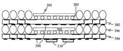
- FIG. 3illustrates a stacked chip-scale ball grid array package using memory dice according to one embodiment of the invention.
- a plurality of the chip-scale ball grid array packages 302 and 304may be vertically stacked with a first surface of a first package 302 being coupled to an opposing second surface of a second package 304 and so on for each successive layer in the stack.
- the contact pads (e.g., 110 in FIG. 1 ) on the second surface of the second package 304are electrically coupled to corresponding pads on the first surface of the first package 302 .
- the solder balls 308have a larger vertical profile or height than the semiconductor die 305 , this permits stacking the first package 302 over the second package 304 .
- a plurality of packagesmay be stacked to increase the density of semiconductor devices that may be mounted on a given area.
- the semiconductor die 301 and 305are memory die
- stacking a plurality of memory devicesincreases the capacity of a memory module in comparison to single-layer chip architectures.
- One aspect of the inventionprovides a chip-scale ball grid array package that permits mounting of components, such as capacitors and resistors, thereon.
- componentssuch as capacitors and resistors
- the surface space above the semiconductor diealways includes pads 306 on which signal conditioning components may be mounted. This surface area may have one or more pads 306 for connecting signal filtering components thereon.
- Thispermits mounting on-chip electrical components 310 , such as capacitors and resistors, which may be used for signal conditioning to and!or from the semiconductor die 305 .
- components 310Being able to mount components 310 on the package substrate itself (e.g., chip-scale substrate) is an advantage over the prior art that was limited to mounting said components only external to the package.
- such components 310are signal conditioning capacitors and pull-up/pull-down resistors.
- FIG. 4illustrates a surface view of a chip-scale ball grid array package with a semiconductor die mounted on a substrate according to a second embodiment of the invention.
- This configurationincludes a substrate 402 with a plurality of solder ball connects 404 and 406 arranged as two columns on either side of a semiconductor die 408 mounted on the substrate 402 .
- the semiconductor die 408may be mounted on the substrate 402 by rigid underside coupling members 410 and 412 , also arranged in two columns along the length of the semiconductor die 408 .
- the underside coupling members 410 and 412are electrically coupled to a plurality of the solder balls 404 and 406 .
- the solder balls 404 and 406are electrically coupled to pads on the opposite surface of the substrate 402 .
- the outboard columns of balls/electrical interconnections(e.g., 404 and 406 ) is two wide per side times whatever length is required to effectively address the maximum number of chip-scale packages to be stacked.
- the basic I/O count required for a typical two hundred and fifty-six (256) Megabyte (Mb) synchronous dynamic (SD) random access memory (RAM) silicon deviceis forty-eight (48), two of which are for unique “addressing”.
- 256Megabyte
- SDsynchronous dynamic random access memory
- RAMrandom access memory
- FIG. 5illustrates a side-view of stacked chip-scale ball grid array packages using memory dice according to a second embodiment of the invention.
- a plurality of chip-scale packages 502 and 504like that illustrated in FIG. 4 , are stacked as shown and in a similar manner to the stacked package described in FIG. 3 .
- Each substrate 502 and 504includes two columns of solder balls 506 along the sides of semiconductor devices 510 and 512 mounted thereon.
- a plurality of underside electrical interconnects 508couples the semiconductor devices 510 and 512 to their respective substrates 502 and 504 .
- Each substratealso includes a plurality of pads 514 on the surface opposite the semiconductor device that may be used to couple signal filtering components 516 .
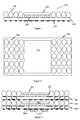
- FIG. 6illustrates a memory module 600 with a plurality of stacked memory components 602 , 604 , 606 , 608 , 610 , and 612 on both surfaces of the memory module 614 according to one embodiment of the invention.
- a plurality of stacked chip-scale ball grid array packages 602 , 604 , 606 , 608 , 610 , and 612may be mounted on one or more surfaces of a substrate 614 .
- the semiconductor devicesmay be random access memory devices mounted on stacked chip-scale packages (e.g., 602 , 604 , 606 , 608 , 610 , and 612 ).
- the stacked packagese.g., 602 , 604 , 606 , 608 , 610 , and 612
- the dimensional requirements of the memory module 600may limit the number of packages (e.g., 100 ) that may be stacked.
- the stacked packagesmay be mounted directly on a computer motherboard or other type of module.
- FIG. 7illustrates a routing scheme for a package stack 700 according to one embodiment of the invention.
- One difficulty in implementing the stackable package architectureis providing a simple way to access each semiconductor device (e.g., memory device) independently.
- Prior art stackable architectureshave typically required customizing the chip-scale package substrate at each level of a stack to enable access to each chip independently. That is, for the same pin on each a chip in a package stack, a different electrical contact must be used at the interface with the module substrate to access each chip independently. This typically necessitates customizing chip-scale package substrates at each level of the stacked packages, with jumpers or trace punching for instance, to provide the appropriate routing from the interface with the module board to the chip.
- manufacturing and assembling such stacked semiconductor chip-scale packagesis costly and cumbersome since customized chip-scale package substrates are typically necessary for each level of the stacked package.
- identical chip-scale package substrates 701 a-dare employed at each level of the stacked package 700 with the semiconductor dice 703 a-d mounted in the same manner on each chip-scale substrate 701 a-d.
- Using identical substrates 701 a-d for every level of the stacked package 700 and mounting the dice 703 a-d in an identical manneravoids the costs and difficulties of having to customize each level.
- a plurality of chip-scale ball grid array packages 701 a-dmay be manufactured and later assembled into a stack without regard as to any particular order.
- the use of identical chip-scale packages at every level of a stack package 700is made possible by a novel routing scheme that permits accessing each semiconductor die 703 a-d independently and without customization of the substrates 701 a-d.
- the novel routing schemeprovides cascading connections through all levels of the stack package 700 to electrically couple each semiconductor die 703 a-d to a primary access point (e.g., the solder balls on substrate 701 a).
- each substrate 701 a-dincludes a plurality of solder balls 705 mounted on a first surface of the substrate 701 a-d and a plurality of corresponding pads 707 on a second opposite surface of the substrate 701 a-d.
- Interconnects 709serve to electrically couple the solder balls 705 to the pads 707 .
- a cascading schemepermits independently accessing each semiconductor die from a primary access point (e.g., the solder balls on substrate 701 a).
- the cascading schemeelectrically couples the solder balls closest to the semiconductor die to a contact on the semiconductor die.
- solder ball 711is electrically coupled to a contact 702 on semiconductor die 703 a.
- This implementation of the routing schemeprovides for solder balls, on a first surface of a chip-scale package substrate, to be electrically coupled to pads, on a second surface of the chip-scale package substrate, that are closer to the semiconductor die.
- solder ball 713is electrically coupled to pad 715 .
- solder balls 717 and 719are coupled to pads that are closer to the semiconductor die 703 a.
- This routing schemeis implemented at every chip-scale package substrate 701 a-d in the stack package 700 .
- each pade.g., 707
- a corresponding solder balle.g., 720
- a cascading routing schemeresults that electrically couples solder balls (e.g., 713 ) in one substrate (e.g., 701 a) to solder balls (e.g., 722 ) in a second substrate (e.g., 701 b) that are closer to the interface point of a semiconductor die.
- solder ball 713is electrically coupled to connect 706
- solder ball 717is electrically coupled to connect 710
- solder ball 719is electrically coupled to connect 714 .
- a similar schememay be implemented on the other side of the semiconductor die such that die connects 704 , 708 , 712 , and 716 are electrically coupled to solder balls on substrate 701 a.
- the stacked package of semiconductor devicesmay then be coupled to another substrate or interface via the solder balls on the first surface of substrate 701 a.
- solder ballsmay be cascaded in different ways and utilizing different solder ball layouts without deviating from the invention.
- a cascading routing schememay be implemented using chip-scale packages similar to that illustrated in FIGS. 4 and 5 .
- the cascading schememay be implemented in two solder ball columns (e.g., 404 ) by zigzagging back and forth between solder balls across multiple package layers to effectively implement the routing scheme illustrated in FIG. 7 . That is, the electrical pad on a first surface of a substrate is electrically coupled to a solder ball on a second surface of the substrate and substantially diagonal relative to the alignment of other pads and solder balls.
- FIGS. 7 and 8may be implemented in various ways, including single column, single row, and/or diagonal/zigzag interconnections across various layers of a stack.
- solder ballsare interconnected using a cascading scheme while part of the remaining solder balls are connected in a non-cascading manner across the stacked package. That is, some of the solder balls in the same position across all layers of a stack may be commonly connected.
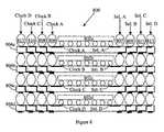
- FIG. 8illustrates a stacked memory package 800 according to one implementation of the invention.
- Memory dice 802 a-dare mounted on chip-scale package substrates 804 a-d.
- the memory components 802 a-dshare common data lines or a bus that serves to write and/or read data (e.g., bits) to and from the memory devices 802 a-d.
- the cascading scheme described in FIG. 7is implemented for individual chip selection and clock enabling.
- the individual packaged memory dice 802 a-dmay be enabled and/or disabled providing an appropriate signal at solder balls 806 - 813 .
- memory device 802 amay be accessed by enabling Clock A at solder ball 806 and chip Select A at solder ball 807 .
- memory device 802 bmay be accessed by enabling Clock B at solder ball 808 and chip Select B at solder ball 809
- memory device 802 cmay be accessed by enabling Clock C at solder ball 810 and chip Select C at solder ball 811
- memory device 802 dmay be accessed by enabling Clock D at solder ball 812 and chip Select D at solder ball 813 .
- the size of a stacked memory or semiconductor packageis limited by the space available on which to mount it in a particular implementation.
- one implementation of the inventionemploys tightly spaced components to maximize semiconductor or memory density of a stack package.
- the substratee.g., 104 in FIG. 2 or 402 in FIG. 4
- the solder ballse.g., 308 in FIG. 3 , or 506 in FIG. 5
- the height or thickness of a particular chip-scale packagee.g., 100 in FIG. 1
- the thickness or height of two stacked chip-scale packagesis approximately 1.00 mm and so forth.
Landscapes
- Engineering & Computer Science (AREA)
- Power Engineering (AREA)
- Microelectronics & Electronic Packaging (AREA)
- Physics & Mathematics (AREA)
- Condensed Matter Physics & Semiconductors (AREA)
- General Physics & Mathematics (AREA)
- Computer Hardware Design (AREA)
- Semiconductor Memories (AREA)
Abstract
Description
- Arlon (Thermount) 85NT, with a coefficient of thermal expansion ranging from 6.0 to 9.0 ppm/° C., depending on the resin contents;
- Arlon (Thermount) 55 NT, with a coefficient of thermal expansion ranging from 7.0 to 10.0 ppm/° C., depending on the resin contents;
- CMC (copper-molybdenum-copper cores), with a baseline coefficient of thermal expansion greater than or equal to 5.5 ppm/° C., where varying the CTE by varying the copper thickness varies this coefficient (e.g., (copper-molybdenum-copper) 5/90/5=5.58 ppm/° C., 13/74/13=5.8 ppm/° C.);
- CIC (copper-Invar-copper) cores, with a baseline coefficient of thermal expansion greater than or equal to 5.1 ppm/° C., where varying the CTE by varying the copper thickness varies this coefficient (e.g., (copper-Invar-copper) 20/60/20=5.2 ppm/° C.);
- Ceramic cores having a coefficient of thermal expansion in the range of 4.5-6.5 ppm/° C. (e.g., AIN at 4.5 and Alumina at 6.5).
Claims (21)
Priority Applications (1)
| Application Number | Priority Date | Filing Date | Title |
|---|---|---|---|
| US12/557,643USRE42363E1 (en) | 2003-09-05 | 2010-02-15 | Stackable electronic assembly |
Applications Claiming Priority (2)
| Application Number | Priority Date | Filing Date | Title |
|---|---|---|---|
| US10/656,452US7180165B2 (en) | 2003-09-05 | 2003-09-05 | Stackable electronic assembly |
| US12/557,643USRE42363E1 (en) | 2003-09-05 | 2010-02-15 | Stackable electronic assembly |
Related Parent Applications (1)
| Application Number | Title | Priority Date | Filing Date |
|---|---|---|---|
| US10/656,452ReissueUS7180165B2 (en) | 2003-09-05 | 2003-09-05 | Stackable electronic assembly |
Publications (1)
| Publication Number | Publication Date |
|---|---|
| USRE42363E1true USRE42363E1 (en) | 2011-05-17 |
Family
ID=34226339
Family Applications (2)
| Application Number | Title | Priority Date | Filing Date |
|---|---|---|---|
| US10/656,452CeasedUS7180165B2 (en) | 2003-09-05 | 2003-09-05 | Stackable electronic assembly |
| US12/557,643Expired - LifetimeUSRE42363E1 (en) | 2003-09-05 | 2010-02-15 | Stackable electronic assembly |
Family Applications Before (1)
| Application Number | Title | Priority Date | Filing Date |
|---|---|---|---|
| US10/656,452CeasedUS7180165B2 (en) | 2003-09-05 | 2003-09-05 | Stackable electronic assembly |
Country Status (6)
| Country | Link |
|---|---|
| US (2) | US7180165B2 (en) |
| EP (1) | EP1685600A4 (en) |
| JP (1) | JP4588027B2 (en) |
| KR (1) | KR100953051B1 (en) |
| CN (1) | CN1846311A (en) |
| WO (1) | WO2005027225A1 (en) |
Cited By (4)
| Publication number | Priority date | Publication date | Assignee | Title |
|---|---|---|---|---|
| US20100090325A1 (en)* | 2008-10-10 | 2010-04-15 | Elpida Memory, Inc. | Semiconductor device |
| US20100200975A1 (en)* | 2009-02-12 | 2010-08-12 | Shinko Electric Industries Co., Ltd. | Semiconductor device and method of manufacturing the same, and electronic apparatus |
| US20110096506A1 (en)* | 2009-10-28 | 2011-04-28 | National Chip Implementation Center National Applied Research Laboratories | Multi-layer soc module structure |
| US20130193582A1 (en)* | 2012-01-27 | 2013-08-01 | Mosaid Technologies Incorporated | Method and apparatus for connecting memory dies to form a memory system |
Families Citing this family (86)
| Publication number | Priority date | Publication date | Assignee | Title |
|---|---|---|---|---|
| US6414391B1 (en)* | 1998-06-30 | 2002-07-02 | Micron Technology, Inc. | Module assembly for stacked BGA packages with a common bus bar in the assembly |
| US7247932B1 (en)* | 2000-05-19 | 2007-07-24 | Megica Corporation | Chip package with capacitor |
| KR100621991B1 (en)* | 2003-01-03 | 2006-09-13 | 삼성전자주식회사 | Chip Scale Stacking Package |
| US7408258B2 (en)* | 2003-08-20 | 2008-08-05 | Salmon Technologies, Llc | Interconnection circuit and electronic module utilizing same |
| US7265446B2 (en)* | 2003-10-06 | 2007-09-04 | Elpida Memory, Inc. | Mounting structure for semiconductor parts and semiconductor device |
| US7183643B2 (en) | 2003-11-04 | 2007-02-27 | Tessera, Inc. | Stacked packages and systems incorporating the same |
| US20050184376A1 (en)* | 2004-02-19 | 2005-08-25 | Salmon Peter C. | System in package |
| US20050205951A1 (en)* | 2004-03-18 | 2005-09-22 | Honeywell Internatioanl, Inc. | Flip chip bonded micro-electromechanical system (MEMS) device |
| US6987314B1 (en) | 2004-06-08 | 2006-01-17 | Amkor Technology, Inc. | Stackable semiconductor package with solder on pads on which second semiconductor package is stacked |
| JP4528062B2 (en)* | 2004-08-25 | 2010-08-18 | 富士通株式会社 | Semiconductor device and manufacturing method thereof |
| US7301242B2 (en)* | 2004-11-04 | 2007-11-27 | Tabula, Inc. | Programmable system in package |
| US7530044B2 (en)* | 2004-11-04 | 2009-05-05 | Tabula, Inc. | Method for manufacturing a programmable system in package |
| US7427809B2 (en)* | 2004-12-16 | 2008-09-23 | Salmon Technologies, Llc | Repairable three-dimensional semiconductor subsystem |
| US20070007983A1 (en)* | 2005-01-06 | 2007-01-11 | Salmon Peter C | Semiconductor wafer tester |
| US20060267174A1 (en)* | 2005-02-09 | 2006-11-30 | William Macropoulos | Apparatus and method using stackable substrates |
| US20080203552A1 (en)* | 2005-02-15 | 2008-08-28 | Unisemicon Co., Ltd. | Stacked Package and Method of Fabricating the Same |
| JP4185499B2 (en)* | 2005-02-18 | 2008-11-26 | 富士通マイクロエレクトロニクス株式会社 | Semiconductor device |
| US8201124B1 (en) | 2005-03-15 | 2012-06-12 | Tabula, Inc. | System in package and method of creating system in package |
| JP4553765B2 (en)* | 2005-03-25 | 2010-09-29 | Okiセミコンダクタ株式会社 | Manufacturing method of semiconductor device |
| TWI264887B (en)* | 2005-05-05 | 2006-10-21 | Universal Scient Ind Co Ltd | Small-form-factor wireless communication module and manufacturing method thereof |
| US7777313B2 (en)* | 2005-06-07 | 2010-08-17 | Analog Devices, Inc. | Electronic package structures and methods |
| US20070023889A1 (en)* | 2005-08-01 | 2007-02-01 | Salmon Peter C | Copper substrate with feedthroughs and interconnection circuits |
| US20070023904A1 (en)* | 2005-08-01 | 2007-02-01 | Salmon Peter C | Electro-optic interconnection apparatus and method |
| US7586747B2 (en)* | 2005-08-01 | 2009-09-08 | Salmon Technologies, Llc. | Scalable subsystem architecture having integrated cooling channels |
| US20070023923A1 (en)* | 2005-08-01 | 2007-02-01 | Salmon Peter C | Flip chip interface including a mixed array of heat bumps and signal bumps |
| JP4553813B2 (en)* | 2005-08-29 | 2010-09-29 | Okiセミコンダクタ株式会社 | Manufacturing method of semiconductor device |
| JP5116268B2 (en)* | 2005-08-31 | 2013-01-09 | キヤノン株式会社 | Multilayer semiconductor device and manufacturing method thereof |
| TWI264127B (en)* | 2005-09-23 | 2006-10-11 | Via Tech Inc | Chip package and substrate thereof |
| TWI305410B (en)* | 2005-10-26 | 2009-01-11 | Advanced Semiconductor Eng | Multi-chip package structure |
| JP4512545B2 (en)* | 2005-10-27 | 2010-07-28 | パナソニック株式会社 | Multilayer semiconductor module |
| TWI270963B (en)* | 2005-12-09 | 2007-01-11 | Via Tech Inc | Package module with alignment structure and electronic device with the same |
| KR100850286B1 (en)* | 2006-01-18 | 2008-08-04 | 삼성전자주식회사 | Semiconductor chip package attached electronic device and integrated circuit module having the same |
| US20070187828A1 (en)* | 2006-02-14 | 2007-08-16 | International Business Machines Corporation | Ild layer with intermediate dielectric constant material immediately below silicon dioxide based ild layer |
| US20070210433A1 (en)* | 2006-03-08 | 2007-09-13 | Rajesh Subraya | Integrated device having a plurality of chip arrangements and method for producing the same |
| US7993969B2 (en)* | 2006-08-10 | 2011-08-09 | Infineon Technologies Ag | Method for producing a module with components stacked one above another |
| US7608921B2 (en)* | 2006-12-07 | 2009-10-27 | Stats Chippac, Inc. | Multi-layer semiconductor package |
| US7532480B1 (en)* | 2006-12-14 | 2009-05-12 | Nvidia Corporation | Power delivery for electronic assemblies |
| KR100885918B1 (en)* | 2007-04-19 | 2009-02-26 | 삼성전자주식회사 | Semiconductor device stack package, electric device and manufacturing method using the same |
| US20080258285A1 (en)* | 2007-04-23 | 2008-10-23 | Texas Instruments Incorporated | Simplified Substrates for Semiconductor Devices in Package-on-Package Products |
| JP4986738B2 (en)* | 2007-06-27 | 2012-07-25 | 新光電気工業株式会社 | Semiconductor package and semiconductor device using the same |
| US7978479B2 (en)* | 2007-08-15 | 2011-07-12 | Accton Technology Corporation | WLAN SiP module |
| KR100927120B1 (en)* | 2007-10-29 | 2009-11-18 | 옵토팩 주식회사 | Semiconductor device packaging method |
| US8779570B2 (en)* | 2008-03-19 | 2014-07-15 | Stats Chippac Ltd. | Stackable integrated circuit package system |
| US8288205B2 (en)* | 2008-03-19 | 2012-10-16 | Stats Chippac Ltd. | Package in package system incorporating an internal stiffener component |
| US8026740B2 (en) | 2008-03-21 | 2011-09-27 | Micron Technology, Inc. | Multi-level signaling for low power, short channel applications |
| US20090268422A1 (en)* | 2008-04-29 | 2009-10-29 | Bailey Mark J | Scalable electronic package assembly for memory devices and other terminated bus structures |
| KR100997272B1 (en)* | 2008-07-17 | 2010-11-29 | 주식회사 동부하이텍 | Semiconductor chip and semiconductor chip stack package |
| US20100019362A1 (en)* | 2008-07-23 | 2010-01-28 | Manolito Galera | Isolated stacked die semiconductor packages |
| US8259461B2 (en) | 2008-11-25 | 2012-09-04 | Micron Technology, Inc. | Apparatus for bypassing faulty connections |
| JP5221315B2 (en)* | 2008-12-17 | 2013-06-26 | 新光電気工業株式会社 | Wiring board and manufacturing method thereof |
| CN101894829B (en)* | 2009-05-19 | 2012-06-27 | 国碁电子(中山)有限公司 | Stacked encapsulating structure |
| KR101078734B1 (en)* | 2009-07-07 | 2011-11-02 | 주식회사 하이닉스반도체 | Semiconductor package and manufacturing method thereof, stack package using same |
| US8169058B2 (en)* | 2009-08-21 | 2012-05-01 | Stats Chippac, Ltd. | Semiconductor device and method of stacking die on leadframe electrically connected by conductive pillars |
| US8383457B2 (en) | 2010-09-03 | 2013-02-26 | Stats Chippac, Ltd. | Semiconductor device and method of forming interposer frame over semiconductor die to provide vertical interconnect |
| USRE48111E1 (en) | 2009-08-21 | 2020-07-21 | JCET Semiconductor (Shaoxing) Co. Ltd. | Semiconductor device and method of forming interposer frame over semiconductor die to provide vertical interconnect |
| US9160349B2 (en) | 2009-08-27 | 2015-10-13 | Micron Technology, Inc. | Die location compensation |
| KR101620347B1 (en)* | 2009-10-14 | 2016-05-13 | 삼성전자주식회사 | Passive elements embedded semiconductor package |
| US8476775B2 (en)* | 2009-12-17 | 2013-07-02 | Stats Chippac Ltd. | Integrated circuit packaging system with embedded interconnect and method of manufacture thereof |
| TWI416700B (en)* | 2009-12-29 | 2013-11-21 | Chipmos Technologies Inc | Chip-stacked package structure and method for manufacturing the same |
| KR20110139983A (en)* | 2010-06-24 | 2011-12-30 | 삼성전자주식회사 | Semiconductor package |
| US9343436B2 (en) | 2010-09-09 | 2016-05-17 | Taiwan Semiconductor Manufacturing Company, Ltd. | Stacked package and method of manufacturing the same |
| US20120063090A1 (en)* | 2010-09-09 | 2012-03-15 | Taiwan Semiconductor Manufacturing Company, Ltd. | Cooling mechanism for stacked die package and method of manufacturing the same |
| US8378477B2 (en)* | 2010-09-14 | 2013-02-19 | Stats Chippac Ltd. | Integrated circuit packaging system with film encapsulation and method of manufacture thereof |
| US8502340B2 (en)* | 2010-12-09 | 2013-08-06 | Tessera, Inc. | High density three-dimensional integrated capacitors |
| KR101321170B1 (en)* | 2010-12-21 | 2013-10-23 | 삼성전기주식회사 | Package and Method for manufacturing the same |
| US8653658B2 (en) | 2011-11-30 | 2014-02-18 | Taiwan Semiconductor Manufacturing Company, Ltd. | Planarized bumps for underfill control |
| US9646942B2 (en) | 2012-02-23 | 2017-05-09 | Taiwan Semiconductor Manufacturing Company, Ltd. | Mechanisms for controlling bump height variation |
| KR101930689B1 (en) | 2012-05-25 | 2018-12-19 | 삼성전자주식회사 | Semiconductor device |
| US8970035B2 (en) | 2012-08-31 | 2015-03-03 | Taiwan Semiconductor Manufacturing Company, Ltd. | Bump structures for semiconductor package |
| CN103000608B (en)* | 2012-12-11 | 2014-11-05 | 矽力杰半导体技术(杭州)有限公司 | Chip packaging structure of a plurality of assemblies |
| US9207275B2 (en)* | 2012-12-14 | 2015-12-08 | International Business Machines Corporation | Interconnect solder bumps for die testing |
| CN104051411B (en)* | 2013-03-15 | 2018-08-28 | 台湾积体电路制造股份有限公司 | Laminated packaging structure |
| TWI555101B (en)* | 2014-05-27 | 2016-10-21 | 矽品精密工業股份有限公司 | Package structure and method of manufacture |
| KR102274742B1 (en)* | 2014-10-06 | 2021-07-07 | 삼성전자주식회사 | PACKAGE ON PACKAGE(PoP) AND COMPUTING DEVICE HAVING THE PoP |
| US9536824B2 (en)* | 2014-11-06 | 2017-01-03 | Origin Gps Ltd. | Dual sided circuit for surface mounting |
| KR102258101B1 (en)* | 2014-12-05 | 2021-05-28 | 삼성전자주식회사 | Package on package and mobile computing device having the same |
| BR112015028568A2 (en)* | 2014-12-15 | 2017-07-25 | Intel Corp | package apparatus in inverted suspension mold package. |
| US11211359B2 (en)* | 2015-09-17 | 2021-12-28 | Semiconductor Components Industries, Llc | Semiconductor device and method of forming modular 3D semiconductor package with horizontal and vertical oriented substrates |
| US9893058B2 (en) | 2015-09-17 | 2018-02-13 | Semiconductor Components Industries, Llc | Method of manufacturing a semiconductor device having reduced on-state resistance and structure |
| US10141938B2 (en)* | 2016-09-21 | 2018-11-27 | Xilinx, Inc. | Stacked columnar integrated circuits |
| KR102701664B1 (en)* | 2019-08-29 | 2024-09-02 | 삼성디스플레이 주식회사 | Display device and manufacturing method thereof |
| CN111128908B (en)* | 2019-11-22 | 2024-04-16 | 中国电子科技集团公司第十三研究所 | Three-dimensional stacked circuit structure and preparation method thereof |
| CN111029324A (en)* | 2019-11-22 | 2020-04-17 | 中国电子科技集团公司第十三研究所 | Three-dimensional microwave module circuit structure and preparation method thereof |
| WO2022209737A1 (en)* | 2021-03-31 | 2022-10-06 | 株式会社村田製作所 | High frequency module and communication device |
| US12002795B2 (en) | 2022-04-13 | 2024-06-04 | Google Llc | Pluggable CPU modules with vertical power |
| US12308543B2 (en) | 2022-04-18 | 2025-05-20 | Google Llc | Structure for optimal XPU socket compression |
Citations (82)
| Publication number | Priority date | Publication date | Assignee | Title |
|---|---|---|---|---|
| US3746934A (en) | 1971-05-06 | 1973-07-17 | Siemens Ag | Stack arrangement of semiconductor chips |
| US4698267A (en)* | 1985-09-17 | 1987-10-06 | E. I. Du Pont De Nemours And Company | High density para-aramid papers |
| US4773868A (en) | 1986-03-19 | 1988-09-27 | Chemie Und Filter Gmbh | Apparatus for use with stackable processor modules |
| US5130894A (en) | 1990-11-26 | 1992-07-14 | At&T Bell Laboratories | Three-dimensional circuit modules |
| US5172303A (en) | 1990-11-23 | 1992-12-15 | Motorola, Inc. | Electronic component assembly |
| US5222014A (en) | 1992-03-02 | 1993-06-22 | Motorola, Inc. | Three-dimensional multi-chip pad array carrier |
| US5334875A (en) | 1987-12-28 | 1994-08-02 | Hitachi, Ltd. | Stacked semiconductor memory device and semiconductor memory module containing the same |
| US5394303A (en) | 1992-09-11 | 1995-02-28 | Kabushiki Kaisha Toshiba | Semiconductor device |
| US5434745A (en) | 1994-07-26 | 1995-07-18 | White Microelectronics Div. Of Bowmar Instrument Corp. | Stacked silicon die carrier assembly |
| US5455385A (en) | 1993-06-28 | 1995-10-03 | Harris Corporation | Multilayer LTCC tub architecture for hermetically sealing semiconductor die, external electrical access for which is provided by way of sidewall recesses |
| US5502667A (en) | 1993-09-13 | 1996-03-26 | International Business Machines Corporation | Integrated multichip memory module structure |
| US5544017A (en) | 1992-08-05 | 1996-08-06 | Fujitsu Limited | Multichip module substrate |
| US5574630A (en)* | 1995-05-11 | 1996-11-12 | International Business Machines Corporation | Laminated electronic package including a power/ground assembly |
| US5586010A (en) | 1995-03-13 | 1996-12-17 | Texas Instruments Incorporated | Low stress ball grid array package |
| US5666272A (en) | 1994-11-29 | 1997-09-09 | Sgs-Thomson Microelectronics, Inc. | Detachable module/ball grid array package |
| US5699234A (en) | 1995-05-30 | 1997-12-16 | General Electric Company | Stacking of three dimensional high density interconnect modules with metal edge contacts |
| US5701233A (en) | 1995-01-23 | 1997-12-23 | Irvine Sensors Corporation | Stackable modules and multimodular assemblies |
| US5712768A (en) | 1992-12-30 | 1998-01-27 | Interconnect Systems, Inc. | Space-saving assemblies for connecting integrated circuits to circuit boards |
| US5715144A (en) | 1994-12-30 | 1998-02-03 | International Business Machines Corporation | Multi-layer, multi-chip pyramid and circuit board structure |
| US5721671A (en) | 1994-10-27 | 1998-02-24 | Gec Alsthom Transport Sa | Subrack for electronic circuit boards and its support |
| US5748452A (en) | 1996-07-23 | 1998-05-05 | International Business Machines Corporation | Multi-electronic device package |
| US5781415A (en) | 1995-08-10 | 1998-07-14 | Nec Corporation | Semiconductor package and mounting method |
| US5783870A (en) | 1995-03-16 | 1998-07-21 | National Semiconductor Corporation | Method for connecting packages of a stacked ball grid array structure |
| US5798567A (en)* | 1997-08-21 | 1998-08-25 | Hewlett-Packard Company | Ball grid array integrated circuit package which employs a flip chip integrated circuit and decoupling capacitors |
| US5854507A (en)* | 1998-07-21 | 1998-12-29 | Hewlett-Packard Company | Multiple chip assembly |
| US5857858A (en) | 1996-12-23 | 1999-01-12 | General Electric Company | Demountable and repairable low pitch interconnect for stacked multichip modules |
| US5883426A (en)* | 1996-04-18 | 1999-03-16 | Nec Corporation | Stack module |
| US5898575A (en) | 1993-12-20 | 1999-04-27 | Lsi Logic Corporation | Support assembly for mounting an integrated circuit package on a surface |
| US5907903A (en) | 1996-05-24 | 1999-06-01 | International Business Machines Corporation | Multi-layer-multi-chip pyramid and circuit board structure and method of forming same |
| US5953210A (en)* | 1997-07-08 | 1999-09-14 | Hughes Electronics Corporation | Reworkable circuit board assembly including a reworkable flip chip |
| US5973392A (en)* | 1997-04-02 | 1999-10-26 | Nec Corporation | Stacked carrier three-dimensional memory module and semiconductor device using the same |
| US5977640A (en)* | 1998-06-26 | 1999-11-02 | International Business Machines Corporation | Highly integrated chip-on-chip packaging |
| US5995379A (en)* | 1997-10-30 | 1999-11-30 | Nec Corporation | Stacked module and substrate therefore |
| US6014316A (en) | 1997-06-13 | 2000-01-11 | Irvine Sensors Corporation | IC stack utilizing BGA contacts |
| US6025648A (en)* | 1997-04-17 | 2000-02-15 | Nec Corporation | Shock resistant semiconductor device and method for producing same |
| US6049467A (en) | 1998-08-31 | 2000-04-11 | Unisys Corporation | Stackable high density RAM modules |
| US6093029A (en) | 1998-09-08 | 2000-07-25 | S3 Incorporated | Vertically stackable integrated circuit |
| US6125039A (en) | 1996-07-31 | 2000-09-26 | Taiyo Yuden Co., Ltd. | Hybrid module |
| US6133626A (en) | 1997-10-10 | 2000-10-17 | Gennum Corporation | Three dimensional packaging configuration for multi-chip module assembly |
| US6137164A (en)* | 1998-03-16 | 2000-10-24 | Texas Instruments Incorporated | Thin stacked integrated circuit device |
| US6163462A (en) | 1997-12-08 | 2000-12-19 | Analog Devices, Inc. | Stress relief substrate for solder ball grid array mounted circuits and method of packaging |
| US6180881B1 (en)* | 1998-05-05 | 2001-01-30 | Harlan Ruben Isaak | Chip stack and method of making same |
| US6188127B1 (en)* | 1995-02-24 | 2001-02-13 | Nec Corporation | Semiconductor packing stack module and method of producing the same |
| US6195268B1 (en) | 1997-06-09 | 2001-02-27 | Floyd K. Eide | Stacking layers containing enclosed IC chips |
| US6222265B1 (en) | 1997-03-10 | 2001-04-24 | Micron Technology, Inc. | Method of constructing stacked packages |
| US6239496B1 (en)* | 1999-01-18 | 2001-05-29 | Kabushiki Kaisha Toshiba | Package having very thin semiconductor chip, multichip module assembled by the package, and method for manufacturing the same |
| US20010008482A1 (en) | 1998-10-15 | 2001-07-19 | David J. Corisis | Integrated device and method for routing a signal through the device |
| US6265772B1 (en) | 1998-06-17 | 2001-07-24 | Nec Corporation | Stacked semiconductor device |
| US6274929B1 (en)* | 1998-09-01 | 2001-08-14 | Texas Instruments Incorporated | Stacked double sided integrated circuit package |
| US6297960B1 (en)* | 1998-06-30 | 2001-10-02 | Micron Technology, Inc. | Heat sink with alignment and retaining features |
| US20010028114A1 (en) | 2000-03-27 | 2001-10-11 | Kabushiki Kaisha Toshiba | Semiconductor device including memory unit and semiconductor module including memory units |
| US6303997B1 (en)* | 1998-04-08 | 2001-10-16 | Anam Semiconductor, Inc. | Thin, stackable semiconductor packages |
| US20010036063A1 (en) | 1998-09-02 | 2001-11-01 | Ibiden Co., Ltd. | Electronic part module mounted on |
| US6331939B1 (en) | 1998-05-04 | 2001-12-18 | Micron Technology, Inc. | Stackable ball grid array package |
| US6339254B1 (en)* | 1998-09-01 | 2002-01-15 | Texas Instruments Incorporated | Stacked flip-chip integrated circuit assemblage |
| US6388333B1 (en)* | 1999-11-30 | 2002-05-14 | Fujitsu Limited | Semiconductor device having protruding electrodes higher than a sealed portion |
| US20020075662A1 (en) | 2000-12-19 | 2002-06-20 | Abocom Systems, Inc. | Stack-type expansible electronic device |
| US6414391B1 (en)* | 1998-06-30 | 2002-07-02 | Micron Technology, Inc. | Module assembly for stacked BGA packages with a common bus bar in the assembly |
| US6437990B1 (en)* | 2000-03-20 | 2002-08-20 | Agere Systems Guardian Corp. | Multi-chip ball grid array IC packages |
| US6448506B1 (en)* | 2000-12-28 | 2002-09-10 | Amkor Technology, Inc. | Semiconductor package and circuit board for making the package |
| US6451624B1 (en)* | 1998-06-05 | 2002-09-17 | Micron Technology, Inc. | Stackable semiconductor package having conductive layer and insulating layers and method of fabrication |
| US6462421B1 (en)* | 2000-04-10 | 2002-10-08 | Advanced Semicondcutor Engineering, Inc. | Multichip module |
| US6477058B1 (en) | 2001-06-28 | 2002-11-05 | Hewlett-Packard Company | Integrated circuit device package including multiple stacked components |
| US20020176233A1 (en) | 2001-02-27 | 2002-11-28 | Stmicroelectronics Limited | Stackable module |
| US6504241B1 (en)* | 1998-10-15 | 2003-01-07 | Sony Corporation | Stackable semiconductor device and method for manufacturing the same |
| US6507107B2 (en)* | 2001-03-15 | 2003-01-14 | Micron Technology, Inc. | Semiconductor/printed circuit board assembly |
| US20030022464A1 (en)* | 2001-07-26 | 2003-01-30 | Naohiko Hirano | Transfer-molded power device and method for manufacturing transfer-molded power device |
| US6521984B2 (en)* | 2000-11-07 | 2003-02-18 | Mitsubishi Denki Kabushiki Kaisha | Semiconductor module with semiconductor devices attached to upper and lower surface of a semiconductor substrate |
| US6522022B2 (en)* | 2000-12-18 | 2003-02-18 | Shinko Electric Industries Co., Ltd. | Mounting structure for semiconductor devices |
| US6525945B1 (en) | 1999-08-20 | 2003-02-25 | International Business Machines Corporation | Method and system for wide band decoupling of integrated circuits |
| US6529385B1 (en) | 1999-08-25 | 2003-03-04 | Intel Corporation | Component array adapter |
| US6531337B1 (en)* | 1998-08-28 | 2003-03-11 | Micron Technology, Inc. | Method of manufacturing a semiconductor structure having stacked semiconductor devices |
| US6538332B2 (en)* | 2000-10-11 | 2003-03-25 | Shinko Electric Industries, Co., Ltd. | Semiconductor device and method of production of same |
| US6542393B1 (en) | 2002-04-24 | 2003-04-01 | Ma Laboratories, Inc. | Dual-bank memory module with stacked DRAM chips having a concave-shaped re-route PCB in-between |
| US6545868B1 (en) | 2000-03-13 | 2003-04-08 | Legacy Electronics, Inc. | Electronic module having canopy-type carriers |
| US6597062B1 (en)* | 2002-08-05 | 2003-07-22 | High Connection Density, Inc. | Short channel, memory module with stacked printed circuit boards |
| US6617695B1 (en)* | 2000-05-30 | 2003-09-09 | Mitsubishi Denki Kabushiki Kaisha | Semiconductor device and semiconductor module using the same |
| US6703697B2 (en)* | 2001-12-07 | 2004-03-09 | Intel Corporation | Electronic package design with improved power delivery performance |
| US6714418B2 (en)* | 2001-11-02 | 2004-03-30 | Infineon Technologies Ag | Method for producing an electronic component having a plurality of chips that are stacked one above the other and contact-connected to one another |
| US6717812B1 (en)* | 2002-11-21 | 2004-04-06 | Institute Of Microelectronics | Apparatus and method for fluid-based cooling of heat-generating devices |
| US6781241B2 (en)* | 2002-04-19 | 2004-08-24 | Fujitsu Limited | Semiconductor device and manufacturing method thereof |
| US6809421B1 (en)* | 1996-12-02 | 2004-10-26 | Kabushiki Kaisha Toshiba | Multichip semiconductor device, chip therefor and method of formation thereof |
Family Cites Families (3)
| Publication number | Priority date | Publication date | Assignee | Title |
|---|---|---|---|---|
| JPH06342874A (en)* | 1993-06-01 | 1994-12-13 | Oki Electric Ind Co Ltd | Semiconductor device high in integration degree |
| JP3358589B2 (en)* | 1999-06-08 | 2002-12-24 | 株式会社村田製作所 | Composition for ceramic substrate, green sheet and ceramic circuit component |
| US7247932B1 (en) | 2000-05-19 | 2007-07-24 | Megica Corporation | Chip package with capacitor |
- 2003
- 2003-09-05USUS10/656,452patent/US7180165B2/ennot_activeCeased
- 2004
- 2004-08-25KRKR1020067004539Apatent/KR100953051B1/ennot_activeExpired - Fee Related
- 2004-08-25WOPCT/US2004/027653patent/WO2005027225A1/enactiveApplication Filing
- 2004-08-25CNCNA200480025558XApatent/CN1846311A/enactivePending
- 2004-08-25EPEP04782199Apatent/EP1685600A4/ennot_activeWithdrawn
- 2004-08-25JPJP2006526125Apatent/JP4588027B2/ennot_activeExpired - Fee Related
- 2010
- 2010-02-15USUS12/557,643patent/USRE42363E1/ennot_activeExpired - Lifetime
Patent Citations (89)
| Publication number | Priority date | Publication date | Assignee | Title |
|---|---|---|---|---|
| US3746934A (en) | 1971-05-06 | 1973-07-17 | Siemens Ag | Stack arrangement of semiconductor chips |
| US4698267A (en)* | 1985-09-17 | 1987-10-06 | E. I. Du Pont De Nemours And Company | High density para-aramid papers |
| US4773868A (en) | 1986-03-19 | 1988-09-27 | Chemie Und Filter Gmbh | Apparatus for use with stackable processor modules |
| US5334875A (en) | 1987-12-28 | 1994-08-02 | Hitachi, Ltd. | Stacked semiconductor memory device and semiconductor memory module containing the same |
| US5172303A (en) | 1990-11-23 | 1992-12-15 | Motorola, Inc. | Electronic component assembly |
| US5130894A (en) | 1990-11-26 | 1992-07-14 | At&T Bell Laboratories | Three-dimensional circuit modules |
| US5222014A (en) | 1992-03-02 | 1993-06-22 | Motorola, Inc. | Three-dimensional multi-chip pad array carrier |
| US5544017A (en) | 1992-08-05 | 1996-08-06 | Fujitsu Limited | Multichip module substrate |
| US5394303A (en) | 1992-09-11 | 1995-02-28 | Kabushiki Kaisha Toshiba | Semiconductor device |
| US5712768A (en) | 1992-12-30 | 1998-01-27 | Interconnect Systems, Inc. | Space-saving assemblies for connecting integrated circuits to circuit boards |
| US5455385A (en) | 1993-06-28 | 1995-10-03 | Harris Corporation | Multilayer LTCC tub architecture for hermetically sealing semiconductor die, external electrical access for which is provided by way of sidewall recesses |
| US5502667A (en) | 1993-09-13 | 1996-03-26 | International Business Machines Corporation | Integrated multichip memory module structure |
| US5702984A (en) | 1993-09-13 | 1997-12-30 | International Business Machines Corporation | Integrated mulitchip memory module, structure and fabrication |
| US5898575A (en) | 1993-12-20 | 1999-04-27 | Lsi Logic Corporation | Support assembly for mounting an integrated circuit package on a surface |
| US5434745A (en) | 1994-07-26 | 1995-07-18 | White Microelectronics Div. Of Bowmar Instrument Corp. | Stacked silicon die carrier assembly |
| US5721671A (en) | 1994-10-27 | 1998-02-24 | Gec Alsthom Transport Sa | Subrack for electronic circuit boards and its support |
| US5666272A (en) | 1994-11-29 | 1997-09-09 | Sgs-Thomson Microelectronics, Inc. | Detachable module/ball grid array package |
| US5715144A (en) | 1994-12-30 | 1998-02-03 | International Business Machines Corporation | Multi-layer, multi-chip pyramid and circuit board structure |
| US5701233A (en) | 1995-01-23 | 1997-12-23 | Irvine Sensors Corporation | Stackable modules and multimodular assemblies |
| US6188127B1 (en)* | 1995-02-24 | 2001-02-13 | Nec Corporation | Semiconductor packing stack module and method of producing the same |
| US5586010A (en) | 1995-03-13 | 1996-12-17 | Texas Instruments Incorporated | Low stress ball grid array package |
| US5783870A (en) | 1995-03-16 | 1998-07-21 | National Semiconductor Corporation | Method for connecting packages of a stacked ball grid array structure |
| US5574630A (en)* | 1995-05-11 | 1996-11-12 | International Business Machines Corporation | Laminated electronic package including a power/ground assembly |
| US5699234A (en) | 1995-05-30 | 1997-12-16 | General Electric Company | Stacking of three dimensional high density interconnect modules with metal edge contacts |
| US5781415A (en) | 1995-08-10 | 1998-07-14 | Nec Corporation | Semiconductor package and mounting method |
| US5883426A (en)* | 1996-04-18 | 1999-03-16 | Nec Corporation | Stack module |
| US5907903A (en) | 1996-05-24 | 1999-06-01 | International Business Machines Corporation | Multi-layer-multi-chip pyramid and circuit board structure and method of forming same |
| US5748452A (en) | 1996-07-23 | 1998-05-05 | International Business Machines Corporation | Multi-electronic device package |
| US5963430A (en) | 1996-07-23 | 1999-10-05 | International Business Machines Corporation | Multi-electronic device package comprising at least two substrates and at least four layers of electrically conductive circuitry |
| US6125039A (en) | 1996-07-31 | 2000-09-26 | Taiyo Yuden Co., Ltd. | Hybrid module |
| US6809421B1 (en)* | 1996-12-02 | 2004-10-26 | Kabushiki Kaisha Toshiba | Multichip semiconductor device, chip therefor and method of formation thereof |
| US5857858A (en) | 1996-12-23 | 1999-01-12 | General Electric Company | Demountable and repairable low pitch interconnect for stacked multichip modules |
| US6583503B2 (en) | 1997-03-10 | 2003-06-24 | Micron Technology, Inc. | Semiconductor package with stacked substrates and multiple semiconductor dice |
| US6222265B1 (en) | 1997-03-10 | 2001-04-24 | Micron Technology, Inc. | Method of constructing stacked packages |
| US5973392A (en)* | 1997-04-02 | 1999-10-26 | Nec Corporation | Stacked carrier three-dimensional memory module and semiconductor device using the same |
| US6025648A (en)* | 1997-04-17 | 2000-02-15 | Nec Corporation | Shock resistant semiconductor device and method for producing same |
| US6195268B1 (en) | 1997-06-09 | 2001-02-27 | Floyd K. Eide | Stacking layers containing enclosed IC chips |
| US6014316A (en) | 1997-06-13 | 2000-01-11 | Irvine Sensors Corporation | IC stack utilizing BGA contacts |
| US5953210A (en)* | 1997-07-08 | 1999-09-14 | Hughes Electronics Corporation | Reworkable circuit board assembly including a reworkable flip chip |
| US5798567A (en)* | 1997-08-21 | 1998-08-25 | Hewlett-Packard Company | Ball grid array integrated circuit package which employs a flip chip integrated circuit and decoupling capacitors |
| US6133626A (en) | 1997-10-10 | 2000-10-17 | Gennum Corporation | Three dimensional packaging configuration for multi-chip module assembly |
| US5995379A (en)* | 1997-10-30 | 1999-11-30 | Nec Corporation | Stacked module and substrate therefore |
| US6163462A (en) | 1997-12-08 | 2000-12-19 | Analog Devices, Inc. | Stress relief substrate for solder ball grid array mounted circuits and method of packaging |
| US6137164A (en)* | 1998-03-16 | 2000-10-24 | Texas Instruments Incorporated | Thin stacked integrated circuit device |
| US6303997B1 (en)* | 1998-04-08 | 2001-10-16 | Anam Semiconductor, Inc. | Thin, stackable semiconductor packages |
| US6549421B2 (en) | 1998-05-04 | 2003-04-15 | Micron Technology, Inc. | Stackable ball grid array package |
| US6331939B1 (en) | 1998-05-04 | 2001-12-18 | Micron Technology, Inc. | Stackable ball grid array package |
| US6180881B1 (en)* | 1998-05-05 | 2001-01-30 | Harlan Ruben Isaak | Chip stack and method of making same |
| US6451624B1 (en)* | 1998-06-05 | 2002-09-17 | Micron Technology, Inc. | Stackable semiconductor package having conductive layer and insulating layers and method of fabrication |
| US6265772B1 (en) | 1998-06-17 | 2001-07-24 | Nec Corporation | Stacked semiconductor device |
| US5977640A (en)* | 1998-06-26 | 1999-11-02 | International Business Machines Corporation | Highly integrated chip-on-chip packaging |
| US6414391B1 (en)* | 1998-06-30 | 2002-07-02 | Micron Technology, Inc. | Module assembly for stacked BGA packages with a common bus bar in the assembly |
| US6297960B1 (en)* | 1998-06-30 | 2001-10-02 | Micron Technology, Inc. | Heat sink with alignment and retaining features |
| US6525943B2 (en)* | 1998-06-30 | 2003-02-25 | Micron Technology, Inc. | Heat sink with alignment and retaining features |
| US5854507A (en)* | 1998-07-21 | 1998-12-29 | Hewlett-Packard Company | Multiple chip assembly |
| US6531337B1 (en)* | 1998-08-28 | 2003-03-11 | Micron Technology, Inc. | Method of manufacturing a semiconductor structure having stacked semiconductor devices |
| US6049467A (en) | 1998-08-31 | 2000-04-11 | Unisys Corporation | Stackable high density RAM modules |
| US6274929B1 (en)* | 1998-09-01 | 2001-08-14 | Texas Instruments Incorporated | Stacked double sided integrated circuit package |
| US6339254B1 (en)* | 1998-09-01 | 2002-01-15 | Texas Instruments Incorporated | Stacked flip-chip integrated circuit assemblage |
| US20010036063A1 (en) | 1998-09-02 | 2001-11-01 | Ibiden Co., Ltd. | Electronic part module mounted on |
| US6093029A (en) | 1998-09-08 | 2000-07-25 | S3 Incorporated | Vertically stackable integrated circuit |
| US6381141B2 (en) | 1998-10-15 | 2002-04-30 | Micron Technology, Inc. | Integrated device and method for routing a signal through the device |
| US20010008482A1 (en) | 1998-10-15 | 2001-07-19 | David J. Corisis | Integrated device and method for routing a signal through the device |
| US6504241B1 (en)* | 1998-10-15 | 2003-01-07 | Sony Corporation | Stackable semiconductor device and method for manufacturing the same |
| US6239496B1 (en)* | 1999-01-18 | 2001-05-29 | Kabushiki Kaisha Toshiba | Package having very thin semiconductor chip, multichip module assembled by the package, and method for manufacturing the same |
| US6525945B1 (en) | 1999-08-20 | 2003-02-25 | International Business Machines Corporation | Method and system for wide band decoupling of integrated circuits |
| US6529385B1 (en) | 1999-08-25 | 2003-03-04 | Intel Corporation | Component array adapter |
| US6388333B1 (en)* | 1999-11-30 | 2002-05-14 | Fujitsu Limited | Semiconductor device having protruding electrodes higher than a sealed portion |
| US6545868B1 (en) | 2000-03-13 | 2003-04-08 | Legacy Electronics, Inc. | Electronic module having canopy-type carriers |
| US6437990B1 (en)* | 2000-03-20 | 2002-08-20 | Agere Systems Guardian Corp. | Multi-chip ball grid array IC packages |
| US6740981B2 (en)* | 2000-03-27 | 2004-05-25 | Kabushiki Kaisha, Toshiba | Semiconductor device including memory unit and semiconductor module including memory units |
| US20010028114A1 (en) | 2000-03-27 | 2001-10-11 | Kabushiki Kaisha Toshiba | Semiconductor device including memory unit and semiconductor module including memory units |
| US6462421B1 (en)* | 2000-04-10 | 2002-10-08 | Advanced Semicondcutor Engineering, Inc. | Multichip module |
| US6617695B1 (en)* | 2000-05-30 | 2003-09-09 | Mitsubishi Denki Kabushiki Kaisha | Semiconductor device and semiconductor module using the same |
| US6538332B2 (en)* | 2000-10-11 | 2003-03-25 | Shinko Electric Industries, Co., Ltd. | Semiconductor device and method of production of same |
| US6521984B2 (en)* | 2000-11-07 | 2003-02-18 | Mitsubishi Denki Kabushiki Kaisha | Semiconductor module with semiconductor devices attached to upper and lower surface of a semiconductor substrate |
| US6522022B2 (en)* | 2000-12-18 | 2003-02-18 | Shinko Electric Industries Co., Ltd. | Mounting structure for semiconductor devices |
| US20020075662A1 (en) | 2000-12-19 | 2002-06-20 | Abocom Systems, Inc. | Stack-type expansible electronic device |
| US6448506B1 (en)* | 2000-12-28 | 2002-09-10 | Amkor Technology, Inc. | Semiconductor package and circuit board for making the package |
| US20020176233A1 (en) | 2001-02-27 | 2002-11-28 | Stmicroelectronics Limited | Stackable module |
| US6507107B2 (en)* | 2001-03-15 | 2003-01-14 | Micron Technology, Inc. | Semiconductor/printed circuit board assembly |
| US6477058B1 (en) | 2001-06-28 | 2002-11-05 | Hewlett-Packard Company | Integrated circuit device package including multiple stacked components |
| US20030022464A1 (en)* | 2001-07-26 | 2003-01-30 | Naohiko Hirano | Transfer-molded power device and method for manufacturing transfer-molded power device |
| US6714418B2 (en)* | 2001-11-02 | 2004-03-30 | Infineon Technologies Ag | Method for producing an electronic component having a plurality of chips that are stacked one above the other and contact-connected to one another |
| US6703697B2 (en)* | 2001-12-07 | 2004-03-09 | Intel Corporation | Electronic package design with improved power delivery performance |
| US6781241B2 (en)* | 2002-04-19 | 2004-08-24 | Fujitsu Limited | Semiconductor device and manufacturing method thereof |
| US6542393B1 (en) | 2002-04-24 | 2003-04-01 | Ma Laboratories, Inc. | Dual-bank memory module with stacked DRAM chips having a concave-shaped re-route PCB in-between |
| US6597062B1 (en)* | 2002-08-05 | 2003-07-22 | High Connection Density, Inc. | Short channel, memory module with stacked printed circuit boards |
| US6717812B1 (en)* | 2002-11-21 | 2004-04-06 | Institute Of Microelectronics | Apparatus and method for fluid-based cooling of heat-generating devices |
Cited By (8)
| Publication number | Priority date | Publication date | Assignee | Title |
|---|---|---|---|---|
| US20100090325A1 (en)* | 2008-10-10 | 2010-04-15 | Elpida Memory, Inc. | Semiconductor device |
| US8288852B2 (en)* | 2008-10-10 | 2012-10-16 | Elpida Memory, Inc. | Semiconductor device |
| US20100200975A1 (en)* | 2009-02-12 | 2010-08-12 | Shinko Electric Industries Co., Ltd. | Semiconductor device and method of manufacturing the same, and electronic apparatus |
| US8344492B2 (en)* | 2009-02-12 | 2013-01-01 | Shinko Electric Industries Co., Ltd. | Semiconductor device and method of manufacturing the same, and electronic apparatus |
| US20110096506A1 (en)* | 2009-10-28 | 2011-04-28 | National Chip Implementation Center National Applied Research Laboratories | Multi-layer soc module structure |
| US8199510B2 (en)* | 2009-10-28 | 2012-06-12 | National Chip Implementation Center | Multi-layer SoC module structure |
| US20130193582A1 (en)* | 2012-01-27 | 2013-08-01 | Mosaid Technologies Incorporated | Method and apparatus for connecting memory dies to form a memory system |
| US9159647B2 (en)* | 2012-01-27 | 2015-10-13 | Novachips Canada Inc. | Method and apparatus for connecting memory dies to form a memory system |
Also Published As
| Publication number | Publication date |
|---|---|
| KR100953051B1 (en) | 2010-04-14 |
| KR20060079207A (en) | 2006-07-05 |
| US20050051903A1 (en) | 2005-03-10 |
| EP1685600A1 (en) | 2006-08-02 |
| JP2007504676A (en) | 2007-03-01 |
| JP4588027B2 (en) | 2010-11-24 |
| US7180165B2 (en) | 2007-02-20 |
| EP1685600A4 (en) | 2008-05-14 |
| WO2005027225A1 (en) | 2005-03-24 |
| CN1846311A (en) | 2006-10-11 |
Similar Documents
| Publication | Publication Date | Title |
|---|---|---|
| USRE42363E1 (en) | Stackable electronic assembly | |
| US6507107B2 (en) | Semiconductor/printed circuit board assembly | |
| US9640515B2 (en) | Multiple die stacking for two or more die | |
| US6838768B2 (en) | Module assembly for stacked BGA packages | |
| US9281266B2 (en) | Stacked chip-on-board module with edge connector | |
| US20050189623A1 (en) | Multiple die package | |
| US20090146283A1 (en) | Stacked-type chip package structure and fabrication method thereof | |
| US7473993B2 (en) | Semiconductor stack package and memory module with improved heat dissipation | |
| US6034425A (en) | Flat multiple-chip module micro ball grid array packaging | |
| US6791193B2 (en) | Chip mounting substrate, first level assembly, and second level assembly | |
| KR20180067695A (en) | High Bandwidth Memory Applications with Controlled Impedance Load | |
| KR100702970B1 (en) | Semiconductor package having binary connection method and manufacturing method thereof | |
| US7217597B2 (en) | Die stacking scheme | |
| KR20050014441A (en) | Semiconductor chip package and stacked module thereof having functional part and packaging part arranged sideways on one plane | |
| US6137174A (en) | Hybrid ASIC/memory module package | |
| US20020050378A1 (en) | Double-layered multiple chip module package | |
| JP2000124389A (en) | Semiconductor mounting board and semiconductor device |
Legal Events
| Date | Code | Title | Description |
|---|---|---|---|
| AS | Assignment | Owner name:US BANK NATIONAL ASSOCIATION, AS NOTES COLLATERAL Free format text:SECURITY INTEREST;ASSIGNORS:SANMINA CORPORATION, AS GRANTOR;SANMINA CORPORATION, F/K/A SANMINA-SCI CORPORATION, AS GRANTOR;HADCO SANTA CLARA, INC., AS GRANTOR;AND OTHERS;REEL/FRAME:033094/0826 Effective date:20140604 | |
| FPAY | Fee payment | Year of fee payment:8 | |
| AS | Assignment | Owner name:SANMINA-SCI CORPORATION, CALIFORNIA Free format text:ASSIGNMENT OF ASSIGNORS INTEREST;ASSIGNOR:SCHMIDT, JON;REEL/FRAME:038661/0580 Effective date:20100208 Owner name:SANMINA-SCI CORPORATION, CALIFORNIA Free format text:ASSIGNMENT OF ASSIGNORS INTEREST;ASSIGNORS:ELLSBERRY, MARK;SCHMITZ, CHARLES E.;CHEN, CHI SHE;AND OTHERS;SIGNING DATES FROM 20040122 TO 20040202;REEL/FRAME:038661/0535 | |
| MAFP | Maintenance fee payment | Free format text:PAYMENT OF MAINTENANCE FEE, 12TH YEAR, LARGE ENTITY (ORIGINAL EVENT CODE: M1553) Year of fee payment:12 | |
| AS | Assignment | Owner name:HADCO CORPORATION, CALIFORNIA Free format text:RELEASE BY SECURED PARTY;ASSIGNOR:U.S. BANK NATIONAL ASSOCIATION, SOLELY AS NOTES COLLATERAL AGENT;REEL/FRAME:049378/0927 Effective date:20190531 Owner name:SANMINA CORPORATION, CALIFORNIA Free format text:RELEASE BY SECURED PARTY;ASSIGNOR:U.S. BANK NATIONAL ASSOCIATION, SOLELY AS NOTES COLLATERAL AGENT;REEL/FRAME:049378/0927 Effective date:20190531 Owner name:SCI TECHNOLOGY, CALIFORNIA Free format text:RELEASE BY SECURED PARTY;ASSIGNOR:U.S. BANK NATIONAL ASSOCIATION, SOLELY AS NOTES COLLATERAL AGENT;REEL/FRAME:049378/0927 Effective date:20190531 Owner name:HADCO SANTA CLARA, CALIFORNIA Free format text:RELEASE BY SECURED PARTY;ASSIGNOR:U.S. BANK NATIONAL ASSOCIATION, SOLELY AS NOTES COLLATERAL AGENT;REEL/FRAME:049378/0927 Effective date:20190531 Owner name:SENSORWISE, INC., CALIFORNIA Free format text:RELEASE BY SECURED PARTY;ASSIGNOR:U.S. BANK NATIONAL ASSOCIATION, SOLELY AS NOTES COLLATERAL AGENT;REEL/FRAME:049378/0927 Effective date:20190531 | |
| AS | Assignment | Owner name:SANMINA CORPORATION, CALIFORNIA Free format text:MERGER;ASSIGNOR:SANMINA-SCI CORPORATION;REEL/FRAME:049890/0797 Effective date:20121115 |