USRE41662E1 - Input power connector for distribution panel - Google Patents
Input power connector for distribution panelDownload PDFInfo
- Publication number
- USRE41662E1 USRE41662E1US11/583,876US58387606AUSRE41662EUS RE41662 E1USRE41662 E1US RE41662E1US 58387606 AUS58387606 AUS 58387606AUS RE41662 EUSRE41662 EUS RE41662E
- Authority
- US
- United States
- Prior art keywords
- power
- cover
- cavity
- housing
- power input
- Prior art date
- Legal status (The legal status is an assumption and is not a legal conclusion. Google has not performed a legal analysis and makes no representation as to the accuracy of the status listed.)
- Expired - Lifetime, expires
Links
Images


Classifications
- H—ELECTRICITY
- H05—ELECTRIC TECHNIQUES NOT OTHERWISE PROVIDED FOR
- H05K—PRINTED CIRCUITS; CASINGS OR CONSTRUCTIONAL DETAILS OF ELECTRIC APPARATUS; MANUFACTURE OF ASSEMBLAGES OF ELECTRICAL COMPONENTS
- H05K7/00—Constructional details common to different types of electric apparatus
- H05K7/14—Mounting supporting structure in casing or on frame or rack
- H05K7/1438—Back panels or connecting means therefor; Terminals; Coding means to avoid wrong insertion
- H05K7/1457—Power distribution arrangements
- H—ELECTRICITY
- H04—ELECTRIC COMMUNICATION TECHNIQUE
- H04Q—SELECTING
- H04Q1/00—Details of selecting apparatus or arrangements
- H04Q1/02—Constructional details
- H04Q1/03—Power distribution arrangements
- H—ELECTRICITY
- H04—ELECTRIC COMMUNICATION TECHNIQUE
- H04M—TELEPHONIC COMMUNICATION
- H04M19/00—Current supply arrangements for telephone systems
- H—ELECTRICITY
- H04—ELECTRIC COMMUNICATION TECHNIQUE
- H04Q—SELECTING
- H04Q2201/00—Constructional details of selecting arrangements
- H04Q2201/10—Housing details
Definitions
- the present inventiongenerally relates to power input structures for power distribution panels.
- Power distribution panelsare generally mounted in an electronic equipment rack with other devices requiring a source of electric power.
- the basic function of such a distribution panelis to receive electric power, typically DC power, from an external power source and distribute this power through a bus bar to a series of individual circuits for delivery to the equipment mounted in the rack or in nearby equipment racks.
- these individual circuitsare protected by fuses or circuit breakers. Common voltages for these panels are 24 and 48 Volts DC.
- the bus barscommonly handle up to 300 amps or more and the individual circuits are protected by circuit breakers capable of handling of up to 100 amps or more or by fuses capable of handling up to 125 amps or more.
- a power distribution panelmay have two separate bus bars, meaning the total current being supplied to a panel could be up to 600 Amps.
- the amount of electrical current being supplied to a power distribution panelis sufficient to cause injury to persons working around these panels or to adjacent devices.
- Protective devices or shieldsare desirable to guard against accidental contact with the exposed power and return current feeds linking the external power sources to the bus bars within the distribution panels.
- these external power feedsmay come from above, below or the side of the distribution panel.
- a distribution panel having a power input structure capable of being easily adapted for receiving and protecting power feeds from multiple directionsis desirable.
- the present inventionrelates to a power input housing with an open ended cavity divided by a centerwall, and a cover for the housing having an extension to close one of the open ends of the cavity when the cover is mounted to the housing.
- a power input assemblyincluding a housing with an open ended cavity divided by a centerwall into return and power chambers with conductors mounted within each chamber.
- a cover for the assemblyis provided having an extension to close one of the open ends of the cavity when the cover is mounted to the housing.
- a further aspect of the present inventionrelates to a method of attaching power input cables to a power distribution panel using a power input assembly including a housing with an open ended cavity divided by a centerwall into power and return chambers with conductors mounted within each chamber and a cover for the housing having an extension to close one of the open ends of the cavity when the cover is mounted to the housing.
- the cablesare led into either one of the open ends and the cover is used to close off the other open end.
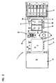
- FIG. 1is a rear perspective view of an embodiment of a power distribution panel in accordance with the present invention.
- FIG. 2is a rear view of the power distribution of FIG. 1 , with the mounting flanges removed.
- FIG. 3is a front view of the power distribution panel of FIG. 1 .
- FIG. 4is a top view of the power distribution panel of FIG. 1 with the top cover removed.
- FIG. 5is a rear perspective view of a power input housing in accordance with the present invention.
- FIG. 6is a front perspective view of the power input housing of FIG. 5 .
- FIG. 7is a front view of the power input housing of FIG. 5 .
- FIG. 8is a rear view of the power input housing of FIG. 5 .
- FIG. 9is a top view of the power input housing of FIG. 5 .
- FIG. 10is a cross-sectional view of the power input housing of FIG. 8 taken along line A—A.
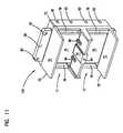
- FIG. 11is a rear perspective view of an alternative power input housing in accordance with the present invention.
- FIG. 12is a front perspective view of the power input housing of FIG. 11 .
- FIG. 13is a front view of the power input housing of FIG. 11 .
- FIG. 14is a rear view of the power input housing of FIG. 11 .
- FIG. 15is a side view of the power input housing of FIG. 11 .
- FIG. 16is a cross-sectional view of the power input housing of FIG. 14 taken along line A—A.
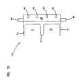
- FIG. 17is an exploded rear view of a power input assembly in accordance with the present invention with the cover positioned for entry of power cables from above the assembly.
- FIG. 18is a rear view of the power input assembly of FIG. 17 with the cover removed.
- FIG. 19is a side view of the power input assembly of FIG. 18 .
- FIG. 19Ais a side view of the power input assembly of FIG. 19 with the cover in a first position.
- FIG. 19Bis a side view of the power input assembly of FIG. 19A with the cover in a second position.
- FIG. 20is a top view of the power input assembly of FIG. 18 .
- FIG. 21is a front perspective view of a cover for a power input assembly in accordance with the present invention.
- FIG. 22is a rear view of the cover of FIG. 21 .
- FIG. 23is a bottom view of the cover of FIG. 21 .
- FIG. 24is a rear perspective view of an alternative power distribution bus in accordance to the present invention for use with the power distribution panel of FIG. 1 .
- FIG. 25is a top view of the power distribution bus of FIG. 24 .
- FIG. 26is a front perspective view of the power distribution bus of FIG. 24 .
- FIG. 27is a front perspective view of a portion of the power distribution bus of FIG. 24 .
- FIG. 28is a rear perspective view of the portion of the power distribution bus of FIG. 26 .
- FIG. 29is a front view of the portion of the power distribution bus of FIG. 26 .
- FIG. 30is a rear view of the portion of the power distribution bus of FIG. 26 .
- FIG. 31is a top view of the portion of the power distribution bus of FIG. 26 .
- FIG. 32is a bottom view of the portion of the power distribution bus of FIG. 26 .
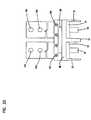
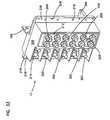
- FIG. 33is a rear perspective view of the power output assembly of FIG. 1 .
- FIG. 34is a top view of the power output assembly of FIG. 33 .
- FIG. 35is a front perspective view of the power output assembly of FIG. 33 .
- a power input assembly 10is provided about each power input location. Assembly 10 is designed to provide separation and isolation of the power or battery and return leads from each other and prevent people and/or other devices from contacting the leads and receiving an electrical shock, causing harm to personnel or property.
- some shielding of the individual power leads 166prevents unwanted arcing or current induction between adjacent leads. This shielding can be accomplished by coating the leads with an electrically insulative material or by providing sufficient separation of the leads. Providing separation of leads 166 also provides improved access to components within panel 1 for users.
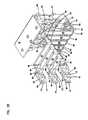
- Panel 1includes a housing with a rear face 28 , a front face 34 , a top 26 , a bottom 44 and two opposing sides 20 .
- Mounted to each side 20 proximate front face 34are mounting flanges 18 for mounting panel 1 to a telecommunications equipment rack. Because telecommunications equipment racks vary in width, flanges 18 include several columns of mounting holes and may be mounted in different orientations.
- Flange 18includes long side 21 and short side 19 . Long side 21 includes two columns of mounting holes 23 and 24 .
- Short side 19includes a single column of mounting holes 22 .
- Panel 1can be mounted to a variety of different width mounting racks by altering the orientation of flanges 18 mounted on either side 20 of panel 1 .
- mounting flanges 18 with short flange 19 adjacent both sides 20would allow panel 1 to mounted to a relatively wider rack, while mounting flanges 18 with long side 21 adjacent sides 20 would permit panel 1 to be mounted to a relatively narrower rack.
- Additional sizes and configurations of flanges 18are anticipated which would permit panel 1 to be mounted to telecommunications racks of different widths.
- Chassis grounds 30are provided on rear face 28 and allow panel 1 to be electrically connected to a ground.
- Panel 1includes an internal circuitry which senses interruptions or other problems with the power flowing through the panel. This circuitry is tied to an alarm which can provide a visible, audible or electronic signal when a power flow problem is detected. The electronic alarm signals allow the alarm status of a power panel to be remotely or centrally monitored.
- Power alarm connector 32is provided on rear face 28 for the transmission of the electronic signals for remote or central monitoring.
- circuit breakers 38 and fuses 42are On the front face of panel 1 to provide protection for the equipment to which panel 1 is supplying power. Additional breaker locations 36 are available to allow more breakers to be mounted to panel 1 . Circuit breakers 38 could alternatively replaced by fuses. Signal lamps 40 are connected with the alarm in panel 1 to provide the visible signal if a power flow problem is detected. Holder 46 is provided on front face 34 to maintain indicia regarding the devices which are being supplied power by panel 1 .
- Power input assembly 10includes a power conductor 52 with posts 48 and a return conductor 54 with posts 50 .
- Conductors 52 and 54are attached to buses 60 inside panel 1 .
- Posts 48are connected with the power terminal of the power source supplying panel 1 and posts 50 are connected with the return terminal of the power source supplying the panel.
- Posts 48are electrically connected to conductor 52 , which are in turn electrically connected with a power bus end 56 of bus 60 .
- Posts 50are electrically connected to conductor 54 , which are in turn electrically connected with a return bus end 58 of bus 60 .
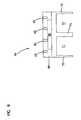
- assembly 10includes a housing 70 with defining a cavity (the housing cavity defined by cavities 71 and 77 ) .
- the housing 70includes opposing sidewalls 72 , a base 76 extending between the sidewalls and a centerwall 74 parallel to the sidewalls and generally bisecting the base into two halves.
- centerwall 74is an opening 94 for receiving a fastener holding cover 14 in place on housing 70 .
- Between sidewalls 72 on either side of centerwall 74are defined the cavities 71 and 77 for receiving power cables from an external power supply.
- Each sidewall 72has a first end 73 and a second end 75 .
- first ends 72are endwall 88 which cooperates with base 76 to form conductor openings 78 proximate first ends 73 .
- endwall 88which cooperates with base 76 to form conductor openings 78 proximate second ends 75 .
- mounting tab 80Extending from each endwall 88 is mounting tab 80 , which include openings 82 to receive fasteners such as screws to mount housing 70 to rear face 28 .
- openings 92are formed opposite base 76 , which receive fasteners such as screws for holding conductors 52 and 54 to housing 70 , as is discussed below.
- reinforcing ribs 84are reinforcing ribs 84 .
- mounting tabs 80are located proximate conductor openings 78 , and cavities 71 and 77 are oriented to receive power cables from above or below panel 1 .
- housing 70is mounted to rear face 28 so that mounting tabs 80 are on the inside of panel 1 and sidewalls 72 and centerwall 74 extend through rear face 28 outside of panel 1 .
- Mounting openings 15 in rear face 28are located above and below housing 70 and are located so that a fastener such as a screw can be inserted through an opening 15 and engage opening 82 to hold housing 70 to rear face 28 .
- housing 170is shown. Housing 170 is similarly constructed to housing 70 , with mounting tabs 80 located on different opposing walls. If housing 170 were mounted to rear face 28 of panel 1 , cavities 71 and 77 would be oriented to receive power cables from either the left side or right side of panel 1 . Both housing 70 and housing 170 are made of electrically insulative material.
- conductors 52 and 54include of a first leg 106 , a cross leg 108 and a second leg 110 .
- First and second legs 106 and 110extend through openings 78 of housing 70 and cross leg 108 lies along the top of base 76 .
- Conductor 52is placed within cavity 71 and conductor 54 is placed within cavity 77 .
- Posts 48extend from cross leg 108 of conductor 52 opposite base 76 and posts 50 extend from cross leg 108 of conductor 54 opposite base 76 .
- Second leg 110 and first leg 106include openings 102 .
- Ledges 124rest just outside of first or second ends 73 or 75 of sidewalls 72 when cover 14 is mounted to housing 70 .
- Ledge 134extends between parallel to extension 122 on the opposite open end of housing 70 but does not extend far enough to close the open end. In this position, cover 14 closes off access to cavities 71 and 77 from the rear and from one of the two ends.
- Ledges 126 and 134are shown as the same size but may be of different sizes. Ledges 126 may extend up to the same extent as extension 122 while ledge 134 may not be made so large as to block the open end opposite extension 122 .
- Mounting opening 128 in top 120includes a narrow end 130 and a wide end 132 . Opening 128 is sized and located to receive a fastener extending from opening 94 in housing 70 to hold cover 14 to housing 70 . The shape of opening 128 is sized to allow cover 14 to be removed from housing 70 without completely removing the screw from opening 94 . Narrow end 130 and wide end 132 are oriented to be generally parallel to ledges 126 .
- Cover 14 and housing 70are designed so that cover 14 may be mounted to housing 70 with extension 122 at either first end 73 (as shown in FIG. 19A ) or second end 75 (as shown in FIG. 19B ) of sidewalls 72 .
- Thiswill permit power supply cables from an external power source to enter from above or below as the installation environment dictates without requiring a different version of cover 14 for each direction of entry.
- housing 170power cables can enter the housing from either end and cover 14 will be installed with extension 122 covering the opposite end.
- Cover 14is made of an electrically insulative material.
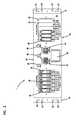
- Three offset connectors 168are located in a first column and three offset connectors 170 169 are located in a second column. This offsetting of adjacent leads and power output connectors provides added space between the connections. This added space reduces the possibility of current in one lead inducing current in an adjacent lead in the area of the connection with power output assembly 12 .
- Leads 166 as shownare crafted from bar stock. To reduce corrosion and other related occurrences, this bar stock may be plated with tin, lead or another suitable material.
- protective device mount 162 and leads 166are shown with the other components of power distribution bus 160 removed.
- Leads 166are individually numbered as leads 171 through 176 , with lead 171 being the topmost lead and lead 176 being the bottommost lead.
- Leads 171 , 173 , and 175are configured to connect with offset connectors 168 of power output assembly 12
- leads 172 , 174 and 176are configured to connect with offset connectors 170 169 .
- Each of the leadsis comprised of five sections, 181 , 183 , 185 , 187 and 189 , connected at four angles, 182 , 184 , 186 and 188 .
- a connector section 181 of each lead 171 through 176is electrically attached to protective device mount 162 .
- An angle 182then links connector segment 181 with a riser segment 183 .
- An angle 184in turn connects riser segment 183 with a twisted segment 185 .
- An angle 186connects twisted segment 185 with a transverse segment 187 .
- An angle 188connects transverse segment 187 with output connector segment 189 .
- Posts 190are mounted on output connector segments 189 to the electrical and physical contact between leads 166 and offset connectors 168 and 170 169 .
- Posts 192are mounted on connector segment 181 to improve electrical and physical contact between leads 166 and protective device mount 162 .
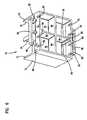
- Output power assembly 12includes an output housing 206 with an inner face 208 and an outer face 210 .
- Return terminals 200 and battery terminals 202are in parallel columns on outer face 210 and located to different planes, 212 and 214 , respectively, to provide separation and improved organization of battery and return cables from telecommunications equipment receiving power from panel 1 .
- output power assembly 12is configured to supply power to six such devices, having six pairs of battery terminals 202 and six pairs of return terminals 200 .
- Alternative configurations having more or fewer pairs of terminalscan be used depending on size constraints and the number of devices requiring power.
- Output housing 206is a uni-body housing, so that the same housing includes provisions for both battery and return terminals.
- Terminals 200 and 202are grouped in pairs to improve the quality and physical surface area of contact between the cables to and from the devices and the terminals, and to prevent rotation of the cables attached to the terminals.
- Return terminals 200are all linked to a common return strap 204 which extends through output housing 206 from outer face 210 beyond inner face 208 . When output power assembly 12 is mounted to panel 1 , return strap 204 is electrically connected to return bus end 58 .
- Each pair of battery terminals 202are connected to a conductor strap 220 which extends through output housing 206 from outer face 210 beyond inner face 208 and includes an offset connector 168 or 170 169 .
- offset connectors 168 and 170 169are electrically connected with segments 189 of leads 166 when output power assembly 12 is mounted to panel 1 .
- Flanges 216 and fastener openings 218are provided on output housing 206 to allow power output assembly 12 to be securely and removably fastened to rear face 28 of panel 1 , as shown in FIG. 1 .
Landscapes
- Engineering & Computer Science (AREA)
- Power Engineering (AREA)
- Microelectronics & Electronic Packaging (AREA)
- Computer Networks & Wireless Communication (AREA)
- Distribution Board (AREA)
Abstract
Description
Claims (38)
Priority Applications (1)
| Application Number | Priority Date | Filing Date | Title |
|---|---|---|---|
| US11/583,876USRE41662E1 (en) | 2001-10-03 | 2006-10-18 | Input power connector for distribution panel |
Applications Claiming Priority (2)
| Application Number | Priority Date | Filing Date | Title |
|---|---|---|---|
| US09/971,083US6806420B2 (en) | 2001-10-03 | 2001-10-03 | Input power connector for distribution panel |
| US11/583,876USRE41662E1 (en) | 2001-10-03 | 2006-10-18 | Input power connector for distribution panel |
Related Parent Applications (1)
| Application Number | Title | Priority Date | Filing Date |
|---|---|---|---|
| US09/971,083ReissueUS6806420B2 (en) | 2001-10-03 | 2001-10-03 | Input power connector for distribution panel |
Publications (1)
| Publication Number | Publication Date |
|---|---|
| USRE41662E1true USRE41662E1 (en) | 2010-09-14 |
Family
ID=25517911
Family Applications (2)
| Application Number | Title | Priority Date | Filing Date |
|---|---|---|---|
| US09/971,083CeasedUS6806420B2 (en) | 2001-10-03 | 2001-10-03 | Input power connector for distribution panel |
| US11/583,876Expired - LifetimeUSRE41662E1 (en) | 2001-10-03 | 2006-10-18 | Input power connector for distribution panel |
Family Applications Before (1)
| Application Number | Title | Priority Date | Filing Date |
|---|---|---|---|
| US09/971,083CeasedUS6806420B2 (en) | 2001-10-03 | 2001-10-03 | Input power connector for distribution panel |
Country Status (3)
| Country | Link |
|---|---|
| US (2) | US6806420B2 (en) |
| AU (1) | AU2002323065A1 (en) |
| WO (1) | WO2003030562A2 (en) |
Cited By (1)
| Publication number | Priority date | Publication date | Assignee | Title |
|---|---|---|---|---|
| US8559167B1 (en)* | 2010-10-04 | 2013-10-15 | Reliance Controls Corporation | Modular Housing for a transfer switch |
Families Citing this family (7)
| Publication number | Priority date | Publication date | Assignee | Title |
|---|---|---|---|---|
| US7005996B2 (en)* | 2002-12-13 | 2006-02-28 | Adc Telecommunications, Inc. | Power distribution panel with modular inserts |
| JP4914434B2 (en)* | 2005-03-17 | 2012-04-11 | リッタル ゲゼルシャフト ミット ベシュレンクテル ハフツング ウント コンパニー コマンディトゲゼルシャフト | Switchboard equipment |
| US7646590B1 (en)* | 2007-07-06 | 2010-01-12 | Exaflop Llc | Data center power distribution |
| US7898787B2 (en)* | 2008-10-09 | 2011-03-01 | Adc Telecommunications, Inc. | Power panel with angled connectors |
| US8154856B2 (en)* | 2009-12-16 | 2012-04-10 | Lineage Power Corporation | Cabinet for a power distribution system |
| EP2607986B1 (en)* | 2011-12-22 | 2014-10-29 | Schroff GmbH | Power feed-in module for a modular computer system |
| CN106489224B (en)* | 2014-02-25 | 2019-12-20 | Abb瑞士股份有限公司 | Horizontal uninterruptible power supply design |
Citations (12)
| Publication number | Priority date | Publication date | Assignee | Title |
|---|---|---|---|---|
| US4867696A (en)* | 1988-07-15 | 1989-09-19 | Amp Incorporated | Laminated bus bar with power tabs |
| EP0735810A2 (en) | 1995-03-28 | 1996-10-02 | The Whitaker Corporation | Pluggable power supply for card cage |
| US5943220A (en) | 1996-09-24 | 1999-08-24 | Sansha Electric Manufacturing Company, Limited | Waterproofed power supply apparatus |
| US5989073A (en)* | 1997-02-05 | 1999-11-23 | General Datacomm, Inc. | Panel feedthrough terminal block assembly |
| US5994989A (en)* | 1998-12-03 | 1999-11-30 | Eaton Corporation | Electrical shorting block with captured spring-biased shorting connectors |
| US6038126A (en) | 1999-04-21 | 2000-03-14 | Shin Jiuh Corp. | Electrical power supply assembly |
| US6081419A (en) | 1998-08-03 | 2000-06-27 | Cisco Technology, Inc. | Protection device for an electronic instrument and method |
| US6315580B1 (en)* | 1999-06-04 | 2001-11-13 | Astec International Limited | PCB connector module for plug-in circuit breakers and fuses |
| US6381122B2 (en)* | 2000-01-15 | 2002-04-30 | Rittal Rudolf Loh Gmbh & Co. Kg | Bus bar system with several bus bars and an installation device with flat connectors |
| US6515227B1 (en) | 2002-05-24 | 2003-02-04 | Alcoa Fujikura Limited | Fiber optic cable management enclosure with integral bend radius control |
| US6548753B1 (en) | 2000-06-06 | 2003-04-15 | Marconi Communications, Inc. | Flame suppression cabinet |
| US6566600B1 (en) | 2001-04-02 | 2003-05-20 | Oem Systems Company, Inc. | Multiple gang junction box assembly with separate lockable divider panels |
- 2001
- 2001-10-03USUS09/971,083patent/US6806420B2/ennot_activeCeased
- 2002
- 2002-08-07WOPCT/US2002/025122patent/WO2003030562A2/ennot_activeApplication Discontinuation
- 2002-08-07AUAU2002323065Apatent/AU2002323065A1/ennot_activeAbandoned
- 2006
- 2006-10-18USUS11/583,876patent/USRE41662E1/ennot_activeExpired - Lifetime
Patent Citations (12)
| Publication number | Priority date | Publication date | Assignee | Title |
|---|---|---|---|---|
| US4867696A (en)* | 1988-07-15 | 1989-09-19 | Amp Incorporated | Laminated bus bar with power tabs |
| EP0735810A2 (en) | 1995-03-28 | 1996-10-02 | The Whitaker Corporation | Pluggable power supply for card cage |
| US5943220A (en) | 1996-09-24 | 1999-08-24 | Sansha Electric Manufacturing Company, Limited | Waterproofed power supply apparatus |
| US5989073A (en)* | 1997-02-05 | 1999-11-23 | General Datacomm, Inc. | Panel feedthrough terminal block assembly |
| US6081419A (en) | 1998-08-03 | 2000-06-27 | Cisco Technology, Inc. | Protection device for an electronic instrument and method |
| US5994989A (en)* | 1998-12-03 | 1999-11-30 | Eaton Corporation | Electrical shorting block with captured spring-biased shorting connectors |
| US6038126A (en) | 1999-04-21 | 2000-03-14 | Shin Jiuh Corp. | Electrical power supply assembly |
| US6315580B1 (en)* | 1999-06-04 | 2001-11-13 | Astec International Limited | PCB connector module for plug-in circuit breakers and fuses |
| US6381122B2 (en)* | 2000-01-15 | 2002-04-30 | Rittal Rudolf Loh Gmbh & Co. Kg | Bus bar system with several bus bars and an installation device with flat connectors |
| US6548753B1 (en) | 2000-06-06 | 2003-04-15 | Marconi Communications, Inc. | Flame suppression cabinet |
| US6566600B1 (en) | 2001-04-02 | 2003-05-20 | Oem Systems Company, Inc. | Multiple gang junction box assembly with separate lockable divider panels |
| US6515227B1 (en) | 2002-05-24 | 2003-02-04 | Alcoa Fujikura Limited | Fiber optic cable management enclosure with integral bend radius control |
Non-Patent Citations (15)
| Title |
|---|
| "PowerWorx(TM) Power Distribution Products", ADC Telecommunications, Inc., 6 pages (Aug. 2000). |
| "PowerWorx(TM) Select Series(TM) Fuse Platform", ADC Telecommunications, Inc., 8 pages (Aug. 2000). |
| "PowerWorx(TM) Traditional GMT Series Power Distribution Panel User Manual", ADC Telecommunications, Inc., ADCP-80-520, Issue 1, pp. 1-33 (Dec. 1999). |
| "PowerWorx® SuperPower(TM) GMT Series", ADC Telecommunications, Inc., 8 pages (Jan. 2001). |
| "PowerWorx® SuperPower™ GMT Series", ADC Telecommunications, Inc., 8 pages (Jan. 2001). |
| "PowerWorx® Traditional GMT Series", ADC Telecommunications, Inc., 8 pages (Jan. 2001). |
| "PowerWorx® Uninterrupted Power GMT Series", ADC Telecommunications, Inc., 8 pages (Jan. 2001). |
| "PowerWorx™ Power Distribution Products", ADC Telecommunications, Inc., 6 pages (Aug. 2000). |
| "PowerWorx™ Select Series™ Fuse Platform", ADC Telecommunications, Inc., 8 pages (Aug. 2000). |
| "PowerWorx™ Traditional GMT Series Power Distribution Panel User Manual", ADC Telecommunications, Inc., ADCP-80-520, Issue 1, pp. 1-33 (Dec. 1999). |
| "Telpower® DC Power Protection Systems. Telpower® Compact Fused Disconnect Switch TPC & TPCDS", Cooper Bussmann, Form No. TPCDS, 2 pages (Sep. 24, 2000). |
| International Preliminary Examination Report (PCT/US02/25122).* |
| International Preliminary Examination Report. |
| Telect, Inc., High Current Power Distribution Alarm Panel Users Manual, Issue A, Rev 1, 46 pages (1999). |
| Telect, Inc., power distribution panel, 17 photographs. |
Cited By (1)
| Publication number | Priority date | Publication date | Assignee | Title |
|---|---|---|---|---|
| US8559167B1 (en)* | 2010-10-04 | 2013-10-15 | Reliance Controls Corporation | Modular Housing for a transfer switch |
Also Published As
| Publication number | Publication date |
|---|---|
| WO2003030562A2 (en) | 2003-04-10 |
| US20030062183A1 (en) | 2003-04-03 |
| US6806420B2 (en) | 2004-10-19 |
| AU2002323065A1 (en) | 2003-04-14 |
| WO2003030562A3 (en) | 2004-03-18 |
Similar Documents
| Publication | Publication Date | Title |
|---|---|---|
| US7458860B2 (en) | Internal power bus and power output assembly | |
| USRE41662E1 (en) | Input power connector for distribution panel | |
| US5574251A (en) | Electrical and electronic cabinet systems | |
| US8038454B2 (en) | Back-mount ganged electrical outlets | |
| US6301095B1 (en) | System and method of distributing power to a plurality of electronic modules housed within an electronics cabinet | |
| EP3243705B1 (en) | Utility vehicle power distribution module | |
| US5515236A (en) | Motor control center universal electrical connector | |
| US7372692B2 (en) | Electrical enclosure and interior assembly therefor | |
| US5627720A (en) | Power distribution box with surge suppressor | |
| US6196869B1 (en) | Mounting bracket and power bus for a connector block | |
| US7306468B2 (en) | Coaxial module with surge protector | |
| US5483409A (en) | 25-pair circuit protection assembly | |
| US7859857B2 (en) | Grounding apparatus | |
| US6291095B1 (en) | Flexible battery mounting and adjustable battery package | |
| US5286210A (en) | Connector interface assembly and method | |
| US6093041A (en) | Connector block with internal power bus | |
| CA2061986A1 (en) | Electric power distribution panelboard-switchboard bus bar insulation shield | |
| US5606489A (en) | Ganged IROB in range out of building protector | |
| JPS6054030A (en) | Terminating frame assembly | |
| KR100907540B1 (en) | Car box | |
| CN213460140U (en) | Through-wall type wiring terminal and low-voltage switch cabinet with same | |
| CN210350719U (en) | Electric circuit management box | |
| CA2077362C (en) | Telecommunications service entry installation | |
| KR20000009592A (en) | Bus bar cover device | |
| MXPA01004491A (en) | Switch/inlet unit and entertainment device |
Legal Events
| Date | Code | Title | Description |
|---|---|---|---|
| CC | Certificate of correction | ||
| FPAY | Fee payment | Year of fee payment:8 | |
| AS | Assignment | Owner name:TYCO ELECTRONICS SERVICES GMBH, SWITZERLAND Free format text:ASSIGNMENT OF ASSIGNORS INTEREST;ASSIGNOR:ADC TELECOMMUNICATIONS, INC.;REEL/FRAME:036060/0174 Effective date:20110930 | |
| AS | Assignment | Owner name:COMMSCOPE EMEA LIMITED, IRELAND Free format text:ASSIGNMENT OF ASSIGNORS INTEREST;ASSIGNOR:TYCO ELECTRONICS SERVICES GMBH;REEL/FRAME:036956/0001 Effective date:20150828 | |
| AS | Assignment | Owner name:COMMSCOPE TECHNOLOGIES LLC, NORTH CAROLINA Free format text:ASSIGNMENT OF ASSIGNORS INTEREST;ASSIGNOR:COMMSCOPE EMEA LIMITED;REEL/FRAME:037012/0001 Effective date:20150828 | |
| AS | Assignment | Owner name:JPMORGAN CHASE BANK, N.A., AS COLLATERAL AGENT, ILLINOIS Free format text:PATENT SECURITY AGREEMENT (TERM);ASSIGNOR:COMMSCOPE TECHNOLOGIES LLC;REEL/FRAME:037513/0709 Effective date:20151220 Owner name:JPMORGAN CHASE BANK, N.A., AS COLLATERAL AGENT, ILLINOIS Free format text:PATENT SECURITY AGREEMENT (ABL);ASSIGNOR:COMMSCOPE TECHNOLOGIES LLC;REEL/FRAME:037514/0196 Effective date:20151220 Owner name:JPMORGAN CHASE BANK, N.A., AS COLLATERAL AGENT, IL Free format text:PATENT SECURITY AGREEMENT (TERM);ASSIGNOR:COMMSCOPE TECHNOLOGIES LLC;REEL/FRAME:037513/0709 Effective date:20151220 Owner name:JPMORGAN CHASE BANK, N.A., AS COLLATERAL AGENT, IL Free format text:PATENT SECURITY AGREEMENT (ABL);ASSIGNOR:COMMSCOPE TECHNOLOGIES LLC;REEL/FRAME:037514/0196 Effective date:20151220 | |
| FPAY | Fee payment | Year of fee payment:12 | |
| AS | Assignment | Owner name:ANDREW LLC, NORTH CAROLINA Free format text:RELEASE BY SECURED PARTY;ASSIGNOR:JPMORGAN CHASE BANK, N.A.;REEL/FRAME:048840/0001 Effective date:20190404 Owner name:COMMSCOPE TECHNOLOGIES LLC, NORTH CAROLINA Free format text:RELEASE BY SECURED PARTY;ASSIGNOR:JPMORGAN CHASE BANK, N.A.;REEL/FRAME:048840/0001 Effective date:20190404 Owner name:REDWOOD SYSTEMS, INC., NORTH CAROLINA Free format text:RELEASE BY SECURED PARTY;ASSIGNOR:JPMORGAN CHASE BANK, N.A.;REEL/FRAME:048840/0001 Effective date:20190404 Owner name:ALLEN TELECOM LLC, ILLINOIS Free format text:RELEASE BY SECURED PARTY;ASSIGNOR:JPMORGAN CHASE BANK, N.A.;REEL/FRAME:048840/0001 Effective date:20190404 Owner name:COMMSCOPE, INC. OF NORTH CAROLINA, NORTH CAROLINA Free format text:RELEASE BY SECURED PARTY;ASSIGNOR:JPMORGAN CHASE BANK, N.A.;REEL/FRAME:048840/0001 Effective date:20190404 Owner name:ALLEN TELECOM LLC, ILLINOIS Free format text:RELEASE BY SECURED PARTY;ASSIGNOR:JPMORGAN CHASE BANK, N.A.;REEL/FRAME:049260/0001 Effective date:20190404 Owner name:COMMSCOPE, INC. OF NORTH CAROLINA, NORTH CAROLINA Free format text:RELEASE BY SECURED PARTY;ASSIGNOR:JPMORGAN CHASE BANK, N.A.;REEL/FRAME:049260/0001 Effective date:20190404 Owner name:ANDREW LLC, NORTH CAROLINA Free format text:RELEASE BY SECURED PARTY;ASSIGNOR:JPMORGAN CHASE BANK, N.A.;REEL/FRAME:049260/0001 Effective date:20190404 Owner name:REDWOOD SYSTEMS, INC., NORTH CAROLINA Free format text:RELEASE BY SECURED PARTY;ASSIGNOR:JPMORGAN CHASE BANK, N.A.;REEL/FRAME:049260/0001 Effective date:20190404 Owner name:COMMSCOPE TECHNOLOGIES LLC, NORTH CAROLINA Free format text:RELEASE BY SECURED PARTY;ASSIGNOR:JPMORGAN CHASE BANK, N.A.;REEL/FRAME:049260/0001 Effective date:20190404 | |
| AS | Assignment | Owner name:WILMINGTON TRUST, NATIONAL ASSOCIATION, AS COLLATE Free format text:PATENT SECURITY AGREEMENT;ASSIGNOR:COMMSCOPE TECHNOLOGIES LLC;REEL/FRAME:049892/0051 Effective date:20190404 Owner name:JPMORGAN CHASE BANK, N.A., NEW YORK Free format text:ABL SECURITY AGREEMENT;ASSIGNORS:COMMSCOPE, INC. OF NORTH CAROLINA;COMMSCOPE TECHNOLOGIES LLC;ARRIS ENTERPRISES LLC;AND OTHERS;REEL/FRAME:049892/0396 Effective date:20190404 Owner name:JPMORGAN CHASE BANK, N.A., NEW YORK Free format text:TERM LOAN SECURITY AGREEMENT;ASSIGNORS:COMMSCOPE, INC. OF NORTH CAROLINA;COMMSCOPE TECHNOLOGIES LLC;ARRIS ENTERPRISES LLC;AND OTHERS;REEL/FRAME:049905/0504 Effective date:20190404 Owner name:WILMINGTON TRUST, NATIONAL ASSOCIATION, AS COLLATERAL AGENT, CONNECTICUT Free format text:PATENT SECURITY AGREEMENT;ASSIGNOR:COMMSCOPE TECHNOLOGIES LLC;REEL/FRAME:049892/0051 Effective date:20190404 | |
| AS | Assignment | Owner name:WILMINGTON TRUST, DELAWARE Free format text:SECURITY INTEREST;ASSIGNORS:ARRIS SOLUTIONS, INC.;ARRIS ENTERPRISES LLC;COMMSCOPE TECHNOLOGIES LLC;AND OTHERS;REEL/FRAME:060752/0001 Effective date:20211115 | |
| AS | Assignment | Owner name:RUCKUS WIRELESS, LLC (F/K/A RUCKUS WIRELESS, INC.), NORTH CAROLINA Free format text:RELEASE OF SECURITY INTEREST AT REEL/FRAME 049905/0504;ASSIGNOR:JPMORGAN CHASE BANK, N.A., AS COLLATERAL AGENT;REEL/FRAME:071477/0255 Effective date:20241217 Owner name:COMMSCOPE TECHNOLOGIES LLC, NORTH CAROLINA Free format text:RELEASE OF SECURITY INTEREST AT REEL/FRAME 049905/0504;ASSIGNOR:JPMORGAN CHASE BANK, N.A., AS COLLATERAL AGENT;REEL/FRAME:071477/0255 Effective date:20241217 Owner name:COMMSCOPE, INC. OF NORTH CAROLINA, NORTH CAROLINA Free format text:RELEASE OF SECURITY INTEREST AT REEL/FRAME 049905/0504;ASSIGNOR:JPMORGAN CHASE BANK, N.A., AS COLLATERAL AGENT;REEL/FRAME:071477/0255 Effective date:20241217 Owner name:ARRIS SOLUTIONS, INC., NORTH CAROLINA Free format text:RELEASE OF SECURITY INTEREST AT REEL/FRAME 049905/0504;ASSIGNOR:JPMORGAN CHASE BANK, N.A., AS COLLATERAL AGENT;REEL/FRAME:071477/0255 Effective date:20241217 Owner name:ARRIS TECHNOLOGY, INC., NORTH CAROLINA Free format text:RELEASE OF SECURITY INTEREST AT REEL/FRAME 049905/0504;ASSIGNOR:JPMORGAN CHASE BANK, N.A., AS COLLATERAL AGENT;REEL/FRAME:071477/0255 Effective date:20241217 Owner name:ARRIS ENTERPRISES LLC (F/K/A ARRIS ENTERPRISES, INC.), NORTH CAROLINA Free format text:RELEASE OF SECURITY INTEREST AT REEL/FRAME 049905/0504;ASSIGNOR:JPMORGAN CHASE BANK, N.A., AS COLLATERAL AGENT;REEL/FRAME:071477/0255 Effective date:20241217 |