USRE41052E1 - Jack including crosstalk compensation for printed circuit board - Google Patents
Jack including crosstalk compensation for printed circuit boardDownload PDFInfo
- Publication number
- USRE41052E1 USRE41052E1US11/732,104US73210407AUSRE41052EUS RE41052 E1USRE41052 E1US RE41052E1US 73210407 AUS73210407 AUS 73210407AUS RE41052 EUSRE41052 EUS RE41052E
- Authority
- US
- United States
- Prior art keywords
- circuit board
- pair
- conductor
- terminals
- capacitors
- Prior art date
- Legal status (The legal status is an assumption and is not a legal conclusion. Google has not performed a legal analysis and makes no representation as to the accuracy of the status listed.)
- Expired - Lifetime
Links
Images


Classifications
- H—ELECTRICITY
- H05—ELECTRIC TECHNIQUES NOT OTHERWISE PROVIDED FOR
- H05K—PRINTED CIRCUITS; CASINGS OR CONSTRUCTIONAL DETAILS OF ELECTRIC APPARATUS; MANUFACTURE OF ASSEMBLAGES OF ELECTRICAL COMPONENTS
- H05K1/00—Printed circuits
- H05K1/02—Details
- H05K1/0213—Electrical arrangements not otherwise provided for
- H05K1/0216—Reduction of cross-talk, noise or electromagnetic interference
- H05K1/0228—Compensation of cross-talk by a mutually correlated lay-out of printed circuit traces, e.g. for compensation of cross-talk in mounted connectors
- H—ELECTRICITY
- H01—ELECTRIC ELEMENTS
- H01R—ELECTRICALLY-CONDUCTIVE CONNECTIONS; STRUCTURAL ASSOCIATIONS OF A PLURALITY OF MUTUALLY-INSULATED ELECTRICAL CONNECTING ELEMENTS; COUPLING DEVICES; CURRENT COLLECTORS
- H01R13/00—Details of coupling devices of the kinds covered by groups H01R12/70 or H01R24/00 - H01R33/00
- H01R13/646—Details of coupling devices of the kinds covered by groups H01R12/70 or H01R24/00 - H01R33/00 specially adapted for high-frequency, e.g. structures providing an impedance match or phase match
- H01R13/6461—Means for preventing cross-talk
- H01R13/6464—Means for preventing cross-talk by adding capacitive elements
- H01R13/6466—Means for preventing cross-talk by adding capacitive elements on substrates, e.g. printed circuit boards [PCB]
- H—ELECTRICITY
- H05—ELECTRIC TECHNIQUES NOT OTHERWISE PROVIDED FOR
- H05K—PRINTED CIRCUITS; CASINGS OR CONSTRUCTIONAL DETAILS OF ELECTRIC APPARATUS; MANUFACTURE OF ASSEMBLAGES OF ELECTRICAL COMPONENTS
- H05K1/00—Printed circuits
- H05K1/16—Printed circuits incorporating printed electric components, e.g. printed resistor, capacitor, inductor
- H05K1/162—Printed circuits incorporating printed electric components, e.g. printed resistor, capacitor, inductor incorporating printed capacitors
- H—ELECTRICITY
- H05—ELECTRIC TECHNIQUES NOT OTHERWISE PROVIDED FOR
- H05K—PRINTED CIRCUITS; CASINGS OR CONSTRUCTIONAL DETAILS OF ELECTRIC APPARATUS; MANUFACTURE OF ASSEMBLAGES OF ELECTRICAL COMPONENTS
- H05K2201/00—Indexing scheme relating to printed circuits covered by H05K1/00
- H05K2201/09—Shape and layout
- H05K2201/09209—Shape and layout details of conductors
- H05K2201/09218—Conductive traces
- H05K2201/09236—Parallel layout
- H—ELECTRICITY
- H05—ELECTRIC TECHNIQUES NOT OTHERWISE PROVIDED FOR
- H05K—PRINTED CIRCUITS; CASINGS OR CONSTRUCTIONAL DETAILS OF ELECTRIC APPARATUS; MANUFACTURE OF ASSEMBLAGES OF ELECTRICAL COMPONENTS
- H05K2201/00—Indexing scheme relating to printed circuits covered by H05K1/00
- H05K2201/10—Details of components or other objects attached to or integrated in a printed circuit board
- H05K2201/10007—Types of components
- H05K2201/10189—Non-printed connector
- Y—GENERAL TAGGING OF NEW TECHNOLOGICAL DEVELOPMENTS; GENERAL TAGGING OF CROSS-SECTIONAL TECHNOLOGIES SPANNING OVER SEVERAL SECTIONS OF THE IPC; TECHNICAL SUBJECTS COVERED BY FORMER USPC CROSS-REFERENCE ART COLLECTIONS [XRACs] AND DIGESTS
- Y10—TECHNICAL SUBJECTS COVERED BY FORMER USPC
- Y10S—TECHNICAL SUBJECTS COVERED BY FORMER USPC CROSS-REFERENCE ART COLLECTIONS [XRACs] AND DIGESTS
- Y10S439/00—Electrical connectors
- Y10S439/941—Crosstalk suppression
Definitions
- the present inventionrelates to electrical connectors, and specifically to electrical connectors having closely spaced contacts and printed circuit boards where interference from crosstalk in the connector is a concern.
- Various electrical connectorsare known for use in the telecommunications industry to transmit voice, data, and video signals. It is common for some electrical connectors to be configured to include a plug which is connectable to a jack mounted in the wall, or as part of a panel or other telecommunications equipment mounted to a rack or cabinet.
- the jackincludes a housing which holds a plurality of closely spaced contact springs in the appropriate position for contacting the contacts of a plug inserted into the jack.
- the contact springs of the jackare often mounted to a printed circuit board, either vertically or horizontally.
- An RJ45 plug and jack connector systemis one well known standard including closely spaced contacts.
- the known method of reducing crosstalkgenerally includes forming of a capacitor by using two parallel conductive lines or wires and inducing electro-magnetic field to compensate the lesser field produced by the capacitive imbalance in the plug. This method is often referred to as capacitance balancing or capacitive compensation.
- the known compensation techniqueis applied at the nearest unbalanced components, which are the contact springs of a jack and the mated RJ45 plug. This technique is very useful for the TIA/EIA category 5 and Enhanced category 5 ( 5 E) connector.
- the crosstalk performance of these connectorsis rated only up to 100 MHz. Higher frequencies are in demand in the telecommunication and data transmission industry.
- the TIA/EIA category 6 connector standardshave been proposed to meet the demand. Under the proposed category 6 standards, the connector is required to meet the crosstalk specifications up to 250 MHz, which is about 150% more bandwidth than the category 5 's.
- the known compensation techniqueis either insufficient to compensate the crosstalk, or problematic by overcompensating for the crosstalk.
- the known compensation techniquehas been considered ineffective when applied to the development of a category 6 or a category 6 type of connector, and particularly, it is unable to meet the crosstalk specifications up to 250 MHz.
- the present inventionprovides a method of compensating crosstalk for a printed circuit board of a connector.
- the present inventionalso provides a connector including such crosstalk compensation method.
- the present method of compensating crosstalk for a printed circuit boardincludes a forward compensation process and a reverse compensation process.
- the forward compensation processcompensates capacitively for the unbalanced capacitance in the plug by forming capacitors, for example, using the parallel conductive lines or wires on the printed circuit board.
- the reverse compensation processcan be used to compensate the unbalanced capacitance and inductance caused by the forward compensations in the same pair combination of the connector. In other words, the reverse compensation negates the forward compensation at the far-end of the printed circuit board by forming capacitors, for example, using the parallel conductive lines or wires, at the far-end of the printed circuit board.
- the method of compensating crosstalk in a connector arrangementincludes: providing a plurality of pairs of conductors on a printed circuit board, the pairs of conductors connecting to respective front and rear terminals, each pair of conductors including a ring conductor and a tip conductor, and the ring and tip conductors being substantially disposed in parallel to control the transmission line impedence; sending electrical signals between the front and rear terminals; generating forward-compensating capacitance, induced between two of the pairs of conductors, proximate the respective front terminals by providing a first capacitor between a first conductor of the first pair and a second conductor of the second pair and providing a second capacitor between a second conductor of the first pair and a first conductor of the second pair; and generating reverse-compensating capacitance/inductance to compensate the unbalanced capacitance/inductance induced between the two pairs of conductors by the first and second capacitors at the front terminal.
- the reverse-compensating capacitance/inductanceis disposed proximate the rear terminals by providing a third capacitor between the first conductor of the first pair and the first conductor of the second pair and providing a fourth capacitor between the second conductor of the first pair and the second conductor of the second pair.
- the capacitance/inductance of the same two pairs of conductorsis compensated at the opposite terminals in the reverse compensation process.
- the forward-reverse compensation techniquecan also be applied to minimize or eliminate crosstalk induced between any other combinations of two pairs of conductors on the printed circuit board.
- One of the advantages of the forward-reverse compensation techniqueis that by reversing the compensations of ones at the opposite terminals, both the far-end crosstalk performance and the near-end crosstalk performance are improved.
- the inductance effect resulted from forming the capacitors at the front terminals of the printed circuit board of the connectoris also balanced.
- FIG. 1is a perspective view of a printed circuit board of one embodiment of the present invention for a telecommunications jack including contact springs at a front portion, and cable terminals at a rear portion;
- FIG. 2is a front end view of a modular jack including the circuit board of FIG. 1 ;
- FIG. 3is a cross-sectional side view of the jack of FIG. 2 , and showing a plug mounted in the opening of the jack;
- FIG. 4is an exploded side view of the jack of FIG. 2 ;
- FIG. 5is a top view of the circuit board of FIG. 1 , with four layers, and showing certain circuit pathways of the four layers of the illustrated preferred embodiment, including the main signal pathways between the front portion and the rear portion of the board, and additional compensation circuit pathways;
- FIG. 6is a top view of the first layer of the circuit board of FIG. 5 ;
- FIG. 7is a top view of the second layer of the circuit board of FIG. 5 ;
- FIG. 8is a top view of the third layer of the circuit board of FIG. 5 ;
- FIG. 9is a top view of the fourth layer of the circuit board of FIG. 5 ;
- FIG. 10is a more complete top view of the circuit board of FIG. 5 showing more of the circuit pathways in the preferred embodiment
- FIG. 11is a top view of the first layer of the circuit board of FIG. 10 ;
- FIG. 12is a top view of the second layer of the circuit board of FIG. 10 ;
- FIG. 13is a top view of the third layer of the circuit board of FIG. 10 ;
- FIG. 14is a top view of the fourth layer of the circuit board of FIG. 10 ;
- FIG. 15is a table showing tip/ring pair connections and polarities applied to the ends or terminals of the tip/ring connections on the circuit board;
- FIG. 16is a table showing pair combinations and capacitance between the pairs of each pair combination
- FIG. 17is an illustration of an example of pin configurations of a typical connector, for example, a RJ45 connector
- FIG. 18is an illustration of capacitance between pairs I and II carried from the plug and compensating capacitance between pairs I and II at both front and rear terminals;
- FIG. 19is an illustration of capacitance between pairs I and II at the front terminals and compensating capacitance between pairs I and II at the rear terminals.
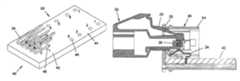
- FIGS. 1-4show an example of a jack 26 constructed in accordance with the principles of the present invention.
- jack 32defines a modular jack construction for mounting to a wall plate, panel or other mounting structure.
- Jack 26defines a port 30 for receiving a plug 32 .
- a plurality of contact springs 34are positioned within port 30 to engage one of a plurality of contacts 36 in the plug 32 .
- the plug 32includes a resilient latch 33 . When the plug 36 is inserted into the port 30 , the latch 33 interlocks with a front tab 35 of the jack 26 to retain the plug 32 within the port 30 . To remove the plug 32 , the latch 33 is depressed thereby allowing the plug 32 to be pulled from the port 30 .
- the jack 26 and plug 32is an 8 contact type (i.e., 4 twisted pair) connector arrangement. While the various aspects of the present invention are particularly useful for 8 contact modular connectors, it will be appreciated that other types of connectors could also be used.
- the jack 26includes a printed circuit board 40 which includes a front portion 42 , and a rear portion 44 .
- the front portion 42includes a plurality of front terminals 46 labeled 1 - 8 .
- the contact springs 34extend from the circuit board 40 at the front terminals 46 to engage the contacts 36 of the plug 32 .
- the rear portion 44 of the circuit board 40includes a plurality of rear terminals 48 labeled 1 - 8 .
- the rear terminals 48are connectable to cables such as through insulation displacement contacts (IDC) 49 .
- IDCinsulation displacement contacts
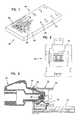
- the jack 26includes a front jack housing 54 , and a rear insert assembly 56 in the illustrated preferred embodiment.
- the jack housing 54is adapted to be snap-fit into a face plate, panel, or other mounting arrangement.
- the insert assembly 56is adapted to snap fit within a back side 61 of the housing 54 .
- the insert assembly 56includes a connector mount 66 , a plurality of insulation displacement terminals 68 , a termination cap 70 , the circuit board 40 , and the contact springs 34 (e.g., eight contact springs) mounted on the circuit board 40 .
- the insulation displacement terminals 68 and the termination cap 70mount at a top side of the connector mount 66
- the circuit board 40mounts to a bottom side of the connector mount 66 .
- the contact springs 34project upward between resilient locking tabs 76 (only one shown) of the connector mount 66 .
- the locking tabs 76are adapted to snap fit within corresponding openings 78 defined by the housing 54 .
- Other spring configurationsare possible, such as those shown in U.S. patent application Ser. No. 09/231,736, filed Jan. 15, 1999 hereby incorporated by reference.
- Other spring configurationsare possible for use with circuit board 40 , as desired.
- front terminals 46are shown in 3 rows across board 40 in the preferred embodiment. Other arrangements are possible such as more or less rows.
- FIG. 3shows the modular plug 32 inserted within the port 30 defined by a front side 84 of the housing 54 .
- the plug 32includes eight contacts 36 that provide electrical connections with the contact springs 34 of the modular jack 26 when the plug 32 is inserted within the port 30 .
- FIG. 3shows one of the contacts 36 in electrical contact with one of the contact springs 34 .
- the contact springs 34are in a deflected orientation, such as that caused by the contacts 36 of plug 32 . In the undeflected orientation, contact springs 34 have their free ends further spaced from board 40 than the illustrated deflected orientation.
- the circuit board 40preferably includes four layers shown in FIGS. 6-9 , respectively. Circuit pathways between front terminals 46 labeled 1 - 8 at the front portion 42 and rear terminals 48 labeled 1 - 8 at the rear portion 44 are all shown in FIG. 5 for explanation purposes.
- FIGS. 6-9illustrate a preferred layout of the circuit pathways in four layers, such that the crossover between the conductive lines or wires is on different layers. The illustrated layout of the pathways conforms with the industry standards.
- the front terminal or pin 46 - 1is connected to the opposite rear terminal or pin 48 - 1 via a transmission path or conductor 50 - 1 .
- the other front terminals or pins 46 -Nare connected to the rear terminals or pins 48 -N, respectively, via transmission paths 50 -N.
- transmission paths 50 - 4 and 50 - 5form a pair I where transmission path 50 - 5 is a tip line, and transmission path 50 - 4 is a ring line;
- transmission path 50 - 3 and 50 - 6form a pair II where transmission path 50 - 3 is a tip line, and transmission path 50 - 6 is a ring line;
- transmission paths 50 - 1 and 50 - 2form a pair III where transmission path 50 - 1 is a tip line, and transmission path 50 - 2 is a ring line;
- transmission paths 50 - 7 and 50 - 8form a pair IV where transmission path 50 - 7 is a ring line, and transmission path 50 - 8 is a ring line.
- the tip terminalgenerally has a positive polarity
- the ring terminalgenerally has a negative polarity.
- the pin assignmentscan be varied without departing from the principle of the present application.
- transmission path 50 - 3 and 50 - 6can be referred to as pair III
- transmission path 50 - 1 and 50 - 2can be referred to as pair II.
- the transmission paths of each pairare substantially parallel to each other.
- the transmission paths 50 - 4 and 50 - 5are parallel; the transmission paths 50 - 3 and 50 - 6 are parallel; the transmission paths 50 - 1 and 50 - 2 are parallel; the transmission paths 50 - 7 and 50 - 8 are parallel.
- Theseare the main signal pathways between the front portion 42 and the rear portion 44 of the circuit board 40 .
- compensation conductive lines 52are added and disposed in parallel to form capacitors 52 -C.
- the added capacitorscompensate the unbalanced capacitance carried from the plug to the front portion 42 of the circuit board 40 .
- FIG. 16a table of capacitance between each two pairs of transmission paths are shown.
- C 34is larger than C 35
- C 65is larger than C 64 .
- the capacitanceis unbalanced between C 34 and C 35 in the I/II pairs.
- the capacitanceis unbalanced between C 65 and C 64 in the I/II pairs.
- FIG. 18The forward compensation is illustrated in FIG. 18 .
- a capacitor C 35 ′is added in dashed lines between terminals 46 - 3 and 46 - 5 , such that the capacitance between terminals 46 - 3 and 46 - 4 and the capacitance between terminals 46 - 3 and 46 - 5 are balanced.
- a capacitor C 64 ′is added in dashed lines between terminals 46 - 4 and 46 - 6 , such that the capacitance between terminals 46 - 4 and 46 - 6 and the capacitance between terminals 46 - 5 and 46 - 6 are balanced.
- the capacitanceis generally minimal due to the isolation provided by the isolation displacement contacts (IDCs) 49 (FIG. 4 ).
- the addition of the capacitors C 35 ′ and C 64 ′causes capacitance/inductance unbalance on the printed circuit board between the front and rear portions.
- a capacitor C 65 ′is further added in dashed lines between rear terminal 48 - 5 and rear terminal 48 - 6 ; and a capacitor C 34 ′ is further added in dashed lines between rear terminal 48 - 3 and rear terminal 48 - 4 , as shown in FIG. 19 .
- C 65 ′ and C 34 ′reverse-compensate the capacitance/inductance unbalance caused by the addition of C 35 ′ and C 64 ′.
- the forward compensationis performed at the front portion 42 .
- the capacitor C 35 ′ between terminal 46 - 3 and terminal 46 - 5is formed by two parallel conductive lines 52 -C 35 ′.
- the capacitor C 64 ′ between terminal 46 - 6 and terminal 46 - 4is formed by two parallel conductive lines 52 -C 64 ′. Additional capacitors, such as 52 -C 64 ′′ and 52 -C 35 ′′, can be used if desired to increase or adjust the capacitance at the front portion 42 .
- the reverse compensationis performed at the rear portion 44 .
- the capacitor C 65 ′ between terminal 48 - 6 and terminal 48 - 5is formed by two parallel conductive lines 52 -C 65 ′.
- the capacitor C 34 ′ between terminal 48 - 3 and terminal 48 - 4is formed by two parallel conductive lines 52 -C 34 ′. It is appreciated that additional capacitors can be used if desired to balance the capacitance/inductance resulted from the front portion 42 .
- the compensating conductive lines 52are terminated on the isolation displacement contacts with a preferable 100 Ohm resistor as generally specified in the industry. It is appreciated that other resistance can be used at the terminal within the scope of the present invention.
- the shape or type of compensating capacitorscan be varied. For example, C 64 ′, C 35 ′, C 34 ′, C 64 ′′, and C 35 ′′ are capacitors formed on the same layer as shown in FIGS. 6-9 . As shown in FIGS. 6-7 , C 65 ′ is formed on two different layers. Also, as shown in FIG. 8 , C 35 ′′ is formed between transmission path 50 - 3 and an additional compensating conductive line 52 - 5 . It is appreciated that other forms of an electro-magnetic field besides capacitors can be used within the scope of the present invention.
- the layer shown in FIG. 6is the first layer of the circuit board 40
- the layer shown in FIG. 7is the second layer of the circuit board 40
- the layer shown in FIG. 8is the third layer of the circuit board 40
- the layer shown in FIG. 9is the fourth layer of the circuit board 40 . It is appreciated that other printed circuit board arrangements can be used without departing from the principles of the present invention.
- the forward-reverse compensation processesallow the capacitance/inductance induced between pair I and pair II to be balanced on the printed circuit board.
- crosstalk caused by the imbalanced capacitance/inductance of pair I and pair IIis minimized or eliminated.
- imbalance capacitance/inductance caused by the other pair combinationssuch as the other five pair combinations shown in FIG. 16 , i.e., I III, II V, II/III, II/IV, and III/IV, can be minimized or eliminated by applying the same principle of the present invention. It is also noted that the imbalance capacitance/inductance caused by pairs III/IV may be negligible due to the far distance between the two pairs.
- FIG. 10illustrates a top view of a more complete capacitance/inductance compensation arrangement on the printed circuit board 40 in a preferred embodiment. It is more complete in a sense that capacitance/inductance imbalance from the other pair combinations (except the combination of pair III and pair IV) are considered. Accordingly, additional capacitors, such as 52 -C 13 ′, can be used to minimize or eliminate the capacitance imbalance induced by pair II and pair III.
- the capacitor C 13 ′is formed by a conductive line 52 -C 13 ′ between the terminal 46 - 1 and the terminal 46 - 3 .
- another capacitorfor example, 52 -C 23 ′, is added to compensate the capacitance/inductance imbalance at the rear portion 44 .
- the capacitors for pair combinationsare 52 -C 46 ′, 52 -C 68 ′, 52 -C 25 ′, 52 -C 65 ′, 52 -C 67 ′, and 52 -C 67 ′′ as shown in FIG. 11 ; 52 -C 68 ′′, 52 -C 58 ′, 52 -C 13 ′′, 52 -C 53 ′, 52 -C 57 ′, 52 -C 23 ′, and 52 -C 15 ′ as shown in FIG. 12 ; 52 -C 47 ′, 52 -C 35 ′, and 52 -C 34 ′ as shown in FIG.
- the layer shown in FIG. 11is the first layer of the circuit board of FIG. 10 .
- the layer shown in FIG. 12is the second layer of the circuit board of FIG. 10 .
- the layer shown in FIG. 13is the third layer of the circuit board of FIG. 10 .
- the layer shown in FIG. 14is the fourth layer of the circuit board of FIG. 10 . It is appreciated that other circuit layer arrangements in the connector can be used within the scope of the present invention.
- forward-reverse compensating techniquecan also be used to compensate unbalanced inductance in the plug and/or contact springs by forming additional capacitors in the reverse compensation process.
- electro-magnetic fieldcan be used to compensate unbalanced capacitance/inductance on the printed circuit board.
- the electro-magnetic fieldcan be a combination of capacitor and inductor.
- capacitors and/or inductors used in the forward-reverse compensation techniquecan be implemented in other parts of the connector, i.e. not necessarily on the printed circuit board, without departing from the principles of the present invention.
- the forward-reverse crosstalk compensation technique of the present inventionsignificantly improves the near-end as well as the far-end crosstalk performance.
- the near-end crosstalkcan be as low as ⁇ 64 dB at 100 MHz frequency and as low as ⁇ 48 at 250 MHz frequency.
- the far-end crosstalkcan be as low as ⁇ 52 dB at 100 MHz frequency and as low as ⁇ 44 dB at 250 MHz.
Landscapes
- Physics & Mathematics (AREA)
- Electromagnetism (AREA)
- Engineering & Computer Science (AREA)
- Microelectronics & Electronic Packaging (AREA)
- Details Of Connecting Devices For Male And Female Coupling (AREA)
- Filters And Equalizers (AREA)
Abstract
Description
Claims (41)
Priority Applications (3)
| Application Number | Priority Date | Filing Date | Title |
|---|---|---|---|
| US11/732,104USRE41052E1 (en) | 1999-08-20 | 2007-04-02 | Jack including crosstalk compensation for printed circuit board |
| US12/806,400USRE43366E1 (en) | 1999-08-20 | 2010-08-11 | Jack including crosstalk compensation for printed circuit board |
| US13/506,644USRE44961E1 (en) | 1999-08-20 | 2012-05-04 | Jack including crosstalk compensation for printed circuit board |
Applications Claiming Priority (4)
| Application Number | Priority Date | Filing Date | Title |
|---|---|---|---|
| US09/378,105US6089923A (en) | 1999-08-20 | 1999-08-20 | Jack including crosstalk compensation for printed circuit board |
| US09/587,939US6428362B1 (en) | 1999-08-20 | 2000-06-06 | Jack including crosstalk compensation for printed circuit board |
| US11/253,281USRE39546E1 (en) | 1999-08-20 | 2005-10-17 | Jack including crosstalk compensation for printed circuit board |
| US11/732,104USRE41052E1 (en) | 1999-08-20 | 2007-04-02 | Jack including crosstalk compensation for printed circuit board |
Related Parent Applications (2)
| Application Number | Title | Priority Date | Filing Date |
|---|---|---|---|
| US09/587,939ReissueUS6428362B1 (en) | 1999-08-20 | 2000-06-06 | Jack including crosstalk compensation for printed circuit board |
| US11/253,281ContinuationUSRE39546E1 (en) | 1999-08-20 | 2005-10-17 | Jack including crosstalk compensation for printed circuit board |
Related Child Applications (1)
| Application Number | Title | Priority Date | Filing Date |
|---|---|---|---|
| US65506509AContinuation | 1999-08-20 | 2009-12-21 |
Publications (1)
| Publication Number | Publication Date |
|---|---|
| USRE41052E1true USRE41052E1 (en) | 2009-12-22 |
Family
ID=23491732
Family Applications (6)
| Application Number | Title | Priority Date | Filing Date |
|---|---|---|---|
| US09/378,105Expired - LifetimeUS6089923A (en) | 1999-08-20 | 1999-08-20 | Jack including crosstalk compensation for printed circuit board |
| US09/587,939CeasedUS6428362B1 (en) | 1999-08-20 | 2000-06-06 | Jack including crosstalk compensation for printed circuit board |
| US11/253,281Expired - LifetimeUSRE39546E1 (en) | 1999-08-20 | 2005-10-17 | Jack including crosstalk compensation for printed circuit board |
| US11/732,104Expired - LifetimeUSRE41052E1 (en) | 1999-08-20 | 2007-04-02 | Jack including crosstalk compensation for printed circuit board |
| US12/806,400Expired - LifetimeUSRE43366E1 (en) | 1999-08-20 | 2010-08-11 | Jack including crosstalk compensation for printed circuit board |
| US13/506,644Expired - LifetimeUSRE44961E1 (en) | 1999-08-20 | 2012-05-04 | Jack including crosstalk compensation for printed circuit board |
Family Applications Before (3)
| Application Number | Title | Priority Date | Filing Date |
|---|---|---|---|
| US09/378,105Expired - LifetimeUS6089923A (en) | 1999-08-20 | 1999-08-20 | Jack including crosstalk compensation for printed circuit board |
| US09/587,939CeasedUS6428362B1 (en) | 1999-08-20 | 2000-06-06 | Jack including crosstalk compensation for printed circuit board |
| US11/253,281Expired - LifetimeUSRE39546E1 (en) | 1999-08-20 | 2005-10-17 | Jack including crosstalk compensation for printed circuit board |
Family Applications After (2)
| Application Number | Title | Priority Date | Filing Date |
|---|---|---|---|
| US12/806,400Expired - LifetimeUSRE43366E1 (en) | 1999-08-20 | 2010-08-11 | Jack including crosstalk compensation for printed circuit board |
| US13/506,644Expired - LifetimeUSRE44961E1 (en) | 1999-08-20 | 2012-05-04 | Jack including crosstalk compensation for printed circuit board |
Country Status (5)
| Country | Link |
|---|---|
| US (6) | US6089923A (en) |
| AR (1) | AR025328A1 (en) |
| AU (1) | AU6528700A (en) |
| TW (1) | TW466806B (en) |
| WO (1) | WO2001015283A1 (en) |
Cited By (4)
| Publication number | Priority date | Publication date | Assignee | Title |
|---|---|---|---|---|
| US20110097935A1 (en)* | 2006-11-14 | 2011-04-28 | Molex Incorporated | Modular jack having a cross talk compensation circuit and robust receptacle terminals |
| USRE43366E1 (en)* | 1999-08-20 | 2012-05-08 | Adc Telecommunications, Inc. | Jack including crosstalk compensation for printed circuit board |
| US20120190240A1 (en)* | 2008-08-20 | 2012-07-26 | Panduit Corp. | High-Speed Connector with Multi-Stage Compensation |
| US20150308412A1 (en)* | 2012-12-06 | 2015-10-29 | Vestas Wind Systems A/S | A three-phase ac electrical sysyem, and a method for compensating an inductance imbalance in such a system |
Families Citing this family (139)
| Publication number | Priority date | Publication date | Assignee | Title |
|---|---|---|---|---|
| GB2331866B (en)* | 1997-11-28 | 2001-08-29 | Nokia Mobile Phones Ltd | Radiotelephone |
| US6356162B1 (en)* | 1999-04-02 | 2002-03-12 | Nordx/Cdt, Inc. | Impedance compensation for a cable and connector |
| JP2002535809A (en)* | 1999-01-15 | 2002-10-22 | エーデーシー・テレコミュニケーションズ・インコーポレーテッド | Communication Jack Assembly |
| US6334792B1 (en) | 1999-01-15 | 2002-01-01 | Adc Telecommunications, Inc. | Connector including reduced crosstalk spring insert |
| US6447326B1 (en)* | 2000-08-09 | 2002-09-10 | Panduit Corp. | Patch cord connector |
| US6520806B2 (en) | 1999-08-20 | 2003-02-18 | Adc Telecommunications, Inc. | Telecommunications connector for high frequency transmissions |
| US7010629B1 (en)* | 1999-12-22 | 2006-03-07 | Intel Corporation | Apparatus and method for coupling to a memory module |
| US6962503B2 (en) | 2000-01-10 | 2005-11-08 | Ortronics, Inc. | Unshielded twisted pair (UTP) wire stabilizer for communication plug |
| US6305950B1 (en)* | 2000-01-14 | 2001-10-23 | Panduit Corp. | Low crosstalk modular communication connector |
| US6190211B1 (en)* | 2000-02-23 | 2001-02-20 | Telebox Industries Corp. | Isolation displacement connector |
| US6533618B1 (en) | 2000-03-31 | 2003-03-18 | Ortronics, Inc. | Bi-directional balance low noise communication interface |
| US6379157B1 (en)* | 2000-08-18 | 2002-04-30 | Leviton Manufacturing Co., Inc. | Communication connector with inductive compensation |
| US6350158B1 (en)* | 2000-09-19 | 2002-02-26 | Avaya Technology Corp. | Low crosstalk communication connector |
| US6802743B2 (en)* | 2000-09-29 | 2004-10-12 | Ortronics, Inc. | Low noise communication modular connector insert |
| US6729901B2 (en) | 2000-09-29 | 2004-05-04 | Ortronics, Inc. | Wire guide sled hardware for communication plug |
| US6554653B2 (en) | 2001-03-16 | 2003-04-29 | Adc Telecommunications, Inc. | Telecommunications connector with spring assembly and method for assembling |
| US6896557B2 (en) | 2001-03-28 | 2005-05-24 | Ortronics, Inc. | Dual reactance low noise modular connector insert |
| US7172466B2 (en)* | 2001-04-05 | 2007-02-06 | Ortronics, Inc. | Dual reactance low noise modular connector insert |
| US6729899B2 (en)* | 2001-05-02 | 2004-05-04 | Ortronics, Inc. | Balance high density 110 IDC terminal block |
| US6413121B1 (en)* | 2001-05-22 | 2002-07-02 | Hon Hai Precision Ind. Co., Ltd. | RJ modular connector having printed circuit board having conductive trace to balance electrical couplings between terminals |
| US6464541B1 (en)* | 2001-05-23 | 2002-10-15 | Avaya Technology Corp. | Simultaneous near-end and far-end crosstalk compensation in a communication connector |
| GB2380334A (en)* | 2001-09-28 | 2003-04-02 | Itt Mfg Enterprises Inc | Communication connector having crosstalk compensating means |
| ATE256347T1 (en)* | 2001-10-29 | 2003-12-15 | Setec Netzwerke Ag | CONNECTION BOX FOR PRODUCING A HIGH PERFORMANCE DATA LINE CONNECTION |
| US6483715B1 (en)* | 2001-11-21 | 2002-11-19 | Surtec Industries Inc. | Circuit board coupled with jacks |
| DE20203910U1 (en) | 2002-03-11 | 2003-07-17 | 3M Innovative Properties Co., St. Paul, Minn. | Connection module for telecommunications technology |
| TW539281U (en)* | 2002-04-19 | 2003-06-21 | Yuan-Huei Peng | Gold needle frame structure |
| DE10242143A1 (en)* | 2002-09-04 | 2004-03-25 | Telegärtner Karl Gärtner GmbH | Electrical socket |
| GB2393858B (en)* | 2002-10-03 | 2004-12-22 | Brand Rex Ltd | Improvements in and relating to electrical connectors |
| US7474737B2 (en)* | 2002-10-10 | 2009-01-06 | The Siemon Company | Telecommunications test plugs having tuned near end crosstalk |
| US6866548B2 (en)* | 2002-10-23 | 2005-03-15 | Avaya Technology Corp. | Correcting for near-end crosstalk unbalance caused by deployment of crosstalk compensation on other pairs |
| US6814624B2 (en)* | 2002-11-22 | 2004-11-09 | Adc Telecommunications, Inc. | Telecommunications jack assembly |
| DE10310434A1 (en)* | 2003-03-11 | 2004-09-30 | Krone Gmbh | Method for RF tuning of an electrical arrangement and a circuit board suitable for this |
| US7265300B2 (en) | 2003-03-21 | 2007-09-04 | Commscope Solutions Properties, Llc | Next high frequency improvement using hybrid substrates of two materials with different dielectric constant frequency slopes |
| US7140924B2 (en)* | 2003-11-21 | 2006-11-28 | Leviton Manufacturing Co., Inc. | Compensation system and method for negative capacitive coupling in IDC |
| US7179131B2 (en) | 2004-02-12 | 2007-02-20 | Panduit Corp. | Methods and apparatus for reducing crosstalk in electrical connectors |
| US20050221678A1 (en) | 2004-02-20 | 2005-10-06 | Hammond Bernard Jr | Methods and systems for compensating for alien crosstalk between connectors |
| US7187766B2 (en) | 2004-02-20 | 2007-03-06 | Adc Incorporated | Methods and systems for compensating for alien crosstalk between connectors |
| US10680385B2 (en) | 2004-02-20 | 2020-06-09 | Commscope Technologies Llc | Methods and systems for compensating for alien crosstalk between connectors |
| KR20070004816A (en)* | 2004-03-03 | 2007-01-09 | 허브벨 인코포레이티드 | Midspan patch panel with data terminal fixture, circuit breaker for power insertion and data acquisition |
| US20050195583A1 (en)* | 2004-03-03 | 2005-09-08 | Hubbell Incorporated. | Midspan patch panel with circuit separation for data terminal equipment, power insertion and data collection |
| US7038918B2 (en)* | 2004-03-03 | 2006-05-02 | Hubbell Incorporated | Midspan patch panel with compensation circuit for data terminal equipment, power insertion and data collection |
| US7342181B2 (en)* | 2004-03-12 | 2008-03-11 | Commscope Inc. Of North Carolina | Maximizing capacitance per unit area while minimizing signal transmission delay in PCB |
| CN1930746B (en) | 2004-03-12 | 2010-12-22 | 泛达公司 | Method and apparatus for reducing crosstalk in an electrical connector |
| US7153168B2 (en)* | 2004-04-06 | 2006-12-26 | Panduit Corp. | Electrical connector with improved crosstalk compensation |
| CA2464834A1 (en)* | 2004-04-19 | 2005-10-19 | Nordx/Cdt Inc. | Connector |
| EP1754316B1 (en)* | 2004-04-27 | 2016-06-08 | Fluke Corporation | Fext cancellation of mated rj45 interconnect |
| US7980900B2 (en)* | 2004-05-14 | 2011-07-19 | Commscope, Inc. Of North Carolina | Next high frequency improvement by using frequency dependent effective capacitance |
| US7190594B2 (en)* | 2004-05-14 | 2007-03-13 | Commscope Solutions Properties, Llc | Next high frequency improvement by using frequency dependent effective capacitance |
| US7038554B2 (en)* | 2004-05-17 | 2006-05-02 | Leviton Manufacturing Co., Inc. | Crosstalk compensation with balancing capacitance system and method |
| US7186149B2 (en)* | 2004-12-06 | 2007-03-06 | Commscope Solutions Properties, Llc | Communications connector for imparting enhanced crosstalk compensation between conductors |
| US7264516B2 (en)* | 2004-12-06 | 2007-09-04 | Commscope, Inc. | Communications jack with printed wiring board having paired coupling conductors |
| US7168993B2 (en) | 2004-12-06 | 2007-01-30 | Commscope Solutions Properties Llc | Communications connector with floating wiring board for imparting crosstalk compensation between conductors |
| US7326089B2 (en)* | 2004-12-07 | 2008-02-05 | Commscope, Inc. Of North Carolina | Communications jack with printed wiring board having self-coupling conductors |
| US7220149B2 (en)* | 2004-12-07 | 2007-05-22 | Commscope Solutions Properties, Llc | Communication plug with balanced wiring to reduce differential to common mode crosstalk |
| US7166000B2 (en)* | 2004-12-07 | 2007-01-23 | Commscope Solutions Properties, Llc | Communications connector with leadframe contact wires that compensate differential to common mode crosstalk |
| US7186148B2 (en)* | 2004-12-07 | 2007-03-06 | Commscope Solutions Properties, Llc | Communications connector for imparting crosstalk compensation between conductors |
| US7204722B2 (en) | 2004-12-07 | 2007-04-17 | Commscope Solutions Properties, Llc | Communications jack with compensation for differential to differential and differential to common mode crosstalk |
| EP1820379B1 (en)* | 2004-12-07 | 2012-10-31 | Commscope Inc. Of North Carolina | Communications jack with printed wiring board having self-coupling conductors |
| US7320624B2 (en)* | 2004-12-16 | 2008-01-22 | Commscope, Inc. Of North Carolina | Communications jacks with compensation for differential to differential and differential to common mode crosstalk |
| WO2006081423A1 (en)* | 2005-01-28 | 2006-08-03 | Commscope Inc. Of North Carolina | Controlled mode conversion connector for reduced alien crosstalk |
| US7314393B2 (en)* | 2005-05-27 | 2008-01-01 | Commscope, Inc. Of North Carolina | Communications connectors with floating wiring board for imparting crosstalk compensation between conductors |
| US7285025B2 (en)* | 2005-07-14 | 2007-10-23 | Tyco Electronics Corporation | Enhanced jack with plug engaging printed circuit board |
| US8011972B2 (en)* | 2006-02-13 | 2011-09-06 | Panduit Corp. | Connector with crosstalk compensation |
| US7488206B2 (en)* | 2006-02-14 | 2009-02-10 | Panduit Corp. | Method and apparatus for patch panel patch cord documentation and revision |
| AU2006202309B2 (en)* | 2006-02-23 | 2011-03-24 | Surtec Industries, Inc. | Connector for communications systems having contact pin arrangement and compensation for improved performance |
| US20070197102A1 (en)* | 2006-02-23 | 2007-08-23 | Hung-Lin Wang | Connector for communications systems having category 6 performance using a single compensation signal or higher performance using plural compensation signals |
| US7402085B2 (en)* | 2006-04-11 | 2008-07-22 | Adc Gmbh | Telecommunications jack with crosstalk compensation provided on a multi-layer circuit board |
| US7787615B2 (en)* | 2006-04-11 | 2010-08-31 | Adc Telecommunications, Inc. | Telecommunications jack with crosstalk compensation and arrangements for reducing return loss |
| US7381098B2 (en) | 2006-04-11 | 2008-06-03 | Adc Telecommunications, Inc. | Telecommunications jack with crosstalk multi-zone crosstalk compensation and method for designing |
| ATE401682T1 (en)* | 2006-05-03 | 2008-08-15 | Ccs Technology Inc | ELECTRICAL CONNECTOR |
| US20070275607A1 (en)* | 2006-05-04 | 2007-11-29 | Kwark Young H | Compensation for far end crosstalk in data buses |
| US7530854B2 (en)* | 2006-06-15 | 2009-05-12 | Ortronics, Inc. | Low noise multiport connector |
| US7410366B2 (en)* | 2006-08-25 | 2008-08-12 | Hon Hai Precision Ind. Co., Ltd. | Electrical connector assembly with reduced crosstalk and electromaganectic interference |
| US7288001B1 (en) | 2006-09-20 | 2007-10-30 | Ortronics, Inc. | Electrically isolated shielded multiport connector assembly |
| US7537484B2 (en) | 2006-10-13 | 2009-05-26 | Adc Gmbh | Connecting hardware with multi-stage inductive and capacitive crosstalk compensation |
| US20080110670A1 (en)* | 2006-11-13 | 2008-05-15 | Yu Cheng Lin | Information jack's circuit board layout |
| US20080141056A1 (en)* | 2006-11-30 | 2008-06-12 | Abughazaleh Shadi A | Asset, PoE and power supply, stack management controller |
| CN103107438B (en)* | 2006-12-01 | 2016-05-04 | 西蒙公司 | The telecommunications plug coordinating with tele-communication jacks |
| AU2007201108B2 (en)* | 2007-03-14 | 2012-02-09 | Tyco Electronics Services Gmbh | Electrical Connector |
| AU2007201114B2 (en)* | 2007-03-14 | 2011-04-07 | Tyco Electronics Services Gmbh | Electrical Connector |
| AU2007201106B9 (en)* | 2007-03-14 | 2011-06-02 | Tyco Electronics Services Gmbh | Electrical Connector |
| AU2007201105B2 (en) | 2007-03-14 | 2011-08-04 | Tyco Electronics Services Gmbh | Electrical Connector |
| AU2007201113B2 (en) | 2007-03-14 | 2011-09-08 | Tyco Electronics Services Gmbh | Electrical Connector |
| AU2007201109B2 (en)* | 2007-03-14 | 2010-11-04 | Tyco Electronics Services Gmbh | Electrical Connector |
| AU2007201102B2 (en)* | 2007-03-14 | 2010-11-04 | Tyco Electronics Services Gmbh | Electrical Connector |
| AU2007201107B2 (en) | 2007-03-14 | 2011-06-23 | Tyco Electronics Services Gmbh | Electrical Connector |
| US7874878B2 (en) | 2007-03-20 | 2011-01-25 | Panduit Corp. | Plug/jack system having PCB with lattice network |
| US7481678B2 (en)* | 2007-06-14 | 2009-01-27 | Ortronics, Inc. | Modular insert and jack including bi-sectional lead frames |
| US7485010B2 (en)* | 2007-06-14 | 2009-02-03 | Ortronics, Inc. | Modular connector exhibiting quad reactance balance functionality |
| CN101378618B (en)* | 2007-08-31 | 2010-09-29 | 鸿富锦精密工业(深圳)有限公司 | A printed circuit board |
| US7824232B2 (en)* | 2008-01-18 | 2010-11-02 | Btx Technologies, Inc. | Multi-position mixed-contact connector with separable modular RJ-45 coupler |
| WO2009100296A1 (en)* | 2008-02-08 | 2009-08-13 | Panduit Corp. | Communications connector with improved contacts |
| US7798857B2 (en)* | 2008-02-12 | 2010-09-21 | Adc Gmbh | Asymmetric crosstalk compensation for improved alien crosstalk performance |
| US7841909B2 (en)* | 2008-02-12 | 2010-11-30 | Adc Gmbh | Multistage capacitive far end crosstalk compensation arrangement |
| DE202008002209U1 (en)* | 2008-02-15 | 2008-04-17 | CCS Technology, Inc., Wilmington | Electrical connector |
| USD612856S1 (en) | 2008-02-20 | 2010-03-30 | Vocollect Healthcare Systems, Inc. | Connector for a peripheral device |
| DE202008017268U1 (en)* | 2008-05-08 | 2009-04-30 | Krones Ag | Electrical plug connection |
| US8113888B2 (en)* | 2008-05-15 | 2012-02-14 | Adc Gmbh | Circuit board for electrical connector and electrical connector |
| AU2009281883A1 (en)* | 2008-08-13 | 2010-02-18 | Panduit Corp. | Communications connector with multi-stage compensation |
| US7914346B2 (en)* | 2008-11-04 | 2011-03-29 | Commscope, Inc. Of North Carolina | Communications jacks having contact wire configurations that provide crosstalk compensation |
| US7682203B1 (en)* | 2008-11-04 | 2010-03-23 | Commscope, Inc. Of North Carolina | Communications jacks having contact wire configurations that provide crosstalk compensation |
| US8202128B2 (en)* | 2008-11-25 | 2012-06-19 | Adc Gmbh | Telecommunications jack with adjustable crosstalk compensation |
| US7794286B2 (en)* | 2008-12-12 | 2010-09-14 | Hubbell Incorporated | Electrical connector with separate contact mounting and compensation boards |
| DE102008064535A1 (en) | 2008-12-19 | 2010-06-24 | Telegärtner Karl Gärtner GmbH | Electrical connector |
| EP2209172A1 (en) | 2009-01-15 | 2010-07-21 | 3M Innovative Properties Company | Telecommunications Jack with a Multilayer PCB |
| US8047879B2 (en)* | 2009-01-26 | 2011-11-01 | Commscope, Inc. Of North Carolina | Printed wiring boards and communication connectors having series inductor-capacitor crosstalk compensation circuits that share a common inductor |
| US8145442B2 (en)* | 2009-01-30 | 2012-03-27 | Synopsys, Inc. | Fast and accurate estimation of gate output loading |
| US7794287B1 (en)* | 2009-04-27 | 2010-09-14 | Hon Hai Precision Ind. Co., Ltd. | Electrical connector configured by wafer having coupling foil and method for making the same |
| US9664711B2 (en) | 2009-07-31 | 2017-05-30 | Pulse Electronics, Inc. | Current sensing devices and methods |
| US9823274B2 (en) | 2009-07-31 | 2017-11-21 | Pulse Electronics, Inc. | Current sensing inductive devices |
| US7967644B2 (en) | 2009-08-25 | 2011-06-28 | Tyco Electronics Corporation | Electrical connector with separable contacts |
| US8016621B2 (en) | 2009-08-25 | 2011-09-13 | Tyco Electronics Corporation | Electrical connector having an electrically parallel compensation region |
| US8128436B2 (en)* | 2009-08-25 | 2012-03-06 | Tyco Electronics Corporation | Electrical connectors with crosstalk compensation |
| US8435082B2 (en) | 2010-08-03 | 2013-05-07 | Tyco Electronics Corporation | Electrical connectors and printed circuits having broadside-coupling regions |
| USD615040S1 (en) | 2009-09-09 | 2010-05-04 | Vocollect, Inc. | Electrical connector |
| US8241053B2 (en)* | 2009-09-10 | 2012-08-14 | Vocollect, Inc. | Electrical cable with strength member |
| US8262403B2 (en) | 2009-09-10 | 2012-09-11 | Vocollect, Inc. | Break-away electrical connector |
| US7850492B1 (en) | 2009-11-03 | 2010-12-14 | Panduit Corp. | Communication connector with improved crosstalk compensation |
| US7828603B1 (en) | 2010-01-07 | 2010-11-09 | Yfc-Boneagle Electric Co., Ltd. | Electrical connector with crosstalk compensation |
| EP2363925A1 (en)* | 2010-01-11 | 2011-09-07 | YFC-Boneagle Electric Co., Ltd. | Electrical connector with crosstalk compensation |
| DE102010014294A1 (en)* | 2010-04-08 | 2011-10-13 | Phoenix Contact Gmbh & Co. Kg | Contact field for connectors |
| US8591262B2 (en) | 2010-09-03 | 2013-11-26 | Pulse Electronics, Inc. | Substrate inductive devices and methods |
| US8425255B2 (en) | 2011-02-04 | 2013-04-23 | Leviton Manufacturing Co., Inc. | Spring assembly with spring members biasing and capacitively coupling jack contacts |
| US8641452B2 (en)* | 2011-03-22 | 2014-02-04 | Panduit Corp. | Communication jack having an insulating element connecting a spring element and a spring end of a contact element |
| CN103022818B (en) | 2011-09-28 | 2015-04-01 | 富士康(昆山)电脑接插件有限公司 | Electric connector |
| EP2783469B1 (en) | 2011-11-23 | 2016-06-22 | Panduit Corp. | Compensation network using an orthogonal compensation network |
| US9531136B2 (en)* | 2012-05-14 | 2016-12-27 | HCS KABLOLAMA SISTEMLERI SAN. ve TIC.A.S. | Keystone jack for use in a computing network |
| US9304149B2 (en) | 2012-05-31 | 2016-04-05 | Pulse Electronics, Inc. | Current sensing devices and methods |
| US9136647B2 (en) | 2012-06-01 | 2015-09-15 | Panduit Corp. | Communication connector with crosstalk compensation |
| US8961238B2 (en) | 2012-09-07 | 2015-02-24 | Commscope, Inc. Of North Carolina | Communication jack with two jackwire contacts mounted on a finger of a flexible printed circuit board |
| US20140125446A1 (en) | 2012-11-07 | 2014-05-08 | Pulse Electronics, Inc. | Substrate inductive device methods and apparatus |
| US9246463B2 (en)* | 2013-03-07 | 2016-01-26 | Panduit Corp. | Compensation networks and communication connectors using said compensation networks |
| US9257792B2 (en) | 2013-03-14 | 2016-02-09 | Panduit Corp. | Connectors and systems having improved crosstalk performance |
| US9246274B2 (en)* | 2013-03-15 | 2016-01-26 | Panduit Corp. | Communication connectors having crosstalk compensation networks |
| US8864532B2 (en) | 2013-03-15 | 2014-10-21 | Commscope, Inc. Of North Carolina | Communications jacks having low crosstalk and/or solder-less wire connection assemblies |
| US9088106B2 (en) | 2013-05-14 | 2015-07-21 | Commscope, Inc. Of North Carolina | Communications jacks having flexible printed circuit boards with common mode crosstalk compensation |
| DE102014104446A1 (en) | 2014-03-28 | 2015-10-01 | Telegärtner Karl Gärtner GmbH | Electrical connector |
| DE102014104449A1 (en) | 2014-03-28 | 2015-10-01 | Telegärtner Karl Gärtner GmbH | Electrical connector |
| US10361514B2 (en)* | 2017-03-02 | 2019-07-23 | Panduit Corp. | Communication connectors utilizing multiple contact points |
Citations (66)
| Publication number | Priority date | Publication date | Assignee | Title |
|---|---|---|---|---|
| US2943272A (en) | 1958-01-02 | 1960-06-28 | Nathan W Feldman | Crosstalk cancellation in signal communication system |
| US3757028A (en) | 1972-09-18 | 1973-09-04 | J Schlessel | Terference printed board and similar transmission line structure for reducing in |
| US3849600A (en) | 1972-10-13 | 1974-11-19 | Sony Corp | Stereophonic signal reproducing apparatus |
| GB1382013A (en) | 1972-04-27 | 1975-01-29 | Philips Electronic Associated | Corsstalk reducing printed circuit board for a switching network |
| US3946165A (en) | 1971-10-06 | 1976-03-23 | Cooper Duane H | Method and apparatus for control of crosstalk in multiple frequency recording |
| US4274691A (en) | 1978-12-05 | 1981-06-23 | Amp Incorporated | Modular jack |
| US4406509A (en) | 1981-11-25 | 1983-09-27 | E. I. Du Pont De Nemours & Co. | Jack and plug electrical assembly |
| US4698025A (en) | 1986-09-15 | 1987-10-06 | Molex Incorporated | Low profile modular phone jack assembly |
| US4767338A (en) | 1987-04-20 | 1988-08-30 | Dennis Melburn W | Printed circuit board telephone interface |
| US4831497A (en) | 1986-09-11 | 1989-05-16 | General Electric Company | Reduction of cross talk in interconnecting conductors |
| US5030123A (en) | 1989-03-24 | 1991-07-09 | Adc Telecommunications, Inc. | Connector and patch panel for digital video and data |
| US5071371A (en) | 1990-03-30 | 1991-12-10 | Molex Incorporated | Electrical card edge connector assembly |
| US5091826A (en) | 1990-03-27 | 1992-02-25 | At&T Bell Laboratories | Printed wiring board connector |
| US5156554A (en) | 1989-10-10 | 1992-10-20 | Itt Corporation | Connector interceptor plate arrangement |
| US5178554A (en) | 1990-10-26 | 1993-01-12 | The Siemon Company | Modular jack patching device |
| US5186647A (en) | 1992-02-24 | 1993-02-16 | At&T Bell Laboratories | High frequency electrical connector |
| US5238426A (en) | 1992-06-11 | 1993-08-24 | At&T Bell Laboratories | Universal patch panel for communications use in buildings |
| US5269708A (en) | 1993-03-03 | 1993-12-14 | Adc Telecommunications, Inc. | Patch panel for high speed twisted pair |
| US5299956A (en) | 1992-03-23 | 1994-04-05 | Superior Modular Products, Inc. | Low cross talk electrical connector system |
| GB2271678A (en) | 1993-12-03 | 1994-04-20 | Itt Ind Ltd | Electrical connector with reduced crosstalk |
| US5326284A (en) | 1992-06-25 | 1994-07-05 | Northern Telecom Limited | Circuit assemblies of printed circuit boards and telecommunications connectors |
| US5362257A (en) | 1993-07-08 | 1994-11-08 | The Whitaker Corporation | Communications connector terminal arrays having noise cancelling capabilities |
| US5362254A (en) | 1992-12-18 | 1994-11-08 | The Siemon Company | Electrically balanced connector assembly |
| US5399107A (en) | 1992-08-20 | 1995-03-21 | Hubbell Incorporated | Modular jack with enhanced crosstalk performance |
| US5414393A (en) | 1992-08-20 | 1995-05-09 | Hubbell Incorporated | Telecommunication connector with feedback |
| US5432484A (en) | 1992-08-20 | 1995-07-11 | Hubbell Incorporated | Connector for communication systems with cancelled crosstalk |
| US5454738A (en) | 1993-10-05 | 1995-10-03 | Thomas & Betts Corporation | Electrical connector having reduced cross-talk |
| US5459643A (en) | 1993-09-30 | 1995-10-17 | The Siemon Company | Electrically enhanced wiring block with break test capability |
| US5488201A (en) | 1994-12-16 | 1996-01-30 | Dan-Chief Enterprise Co., Ltd. | Low crosstalk electrical signal transmission medium |
| US5562479A (en) | 1993-08-31 | 1996-10-08 | At&T Corp. | Connector for unshielded twisted wire pair cables |
| WO1996037017A1 (en) | 1995-05-19 | 1996-11-21 | The Whitaker Corporation | An electrical connector and an associated method for compensating for crosstalk between a plurality of conductors |
| US5580257A (en) | 1995-04-28 | 1996-12-03 | Molex Incorporated | High performance card edge connector |
| US5580270A (en) | 1992-11-16 | 1996-12-03 | Krone Ag | Electrical plug connector |
| US5626497A (en) | 1994-07-14 | 1997-05-06 | Molex Incorporated | Modular jack type connector |
| US5628647A (en) | 1995-02-22 | 1997-05-13 | Stewart Connector Systems, Inc. | High frequency modular plug and cable assembly |
| US5639266A (en) | 1994-01-11 | 1997-06-17 | Stewart Connector Systems, Inc. | High frequency electrical connector |
| US5663870A (en) | 1994-08-09 | 1997-09-02 | Krone Aktiengesellschaft | Printed circuit board for connectors |
| US5674093A (en) | 1996-07-23 | 1997-10-07 | Superior Modular Process Incorporated | Reduced cross talk electrical connector |
| US5679027A (en) | 1992-09-04 | 1997-10-21 | Pressac Ltd. | Apparatus for crosstalk cancellation in data connectors |
| US5700167A (en) | 1996-09-06 | 1997-12-23 | Lucent Technologies | Connector cross-talk compensation |
| GB2314466A (en) | 1996-06-21 | 1997-12-24 | Lucent Technologies Inc | Capacitor array for reducing cross-talk in connectors |
| US5713764A (en) | 1992-03-16 | 1998-02-03 | Molex Incorporated | Impedance and inductance control in electrical connectors |
| US5716237A (en) | 1996-06-21 | 1998-02-10 | Lucent Technologies Inc. | Electrical connector with crosstalk compensation |
| US5735714A (en) | 1995-04-06 | 1998-04-07 | Ortronics Inc. | Information management outlet module and assembly providing protection to exposed cabling |
| US5759070A (en) | 1994-11-30 | 1998-06-02 | Berg Technology, Inc. | Modular jack insert |
| US5779503A (en) | 1996-12-18 | 1998-07-14 | Nordx/Cdt, Inc. | High frequency connector with noise cancelling characteristics |
| US5791943A (en) | 1995-11-22 | 1998-08-11 | The Siemon Company | Reduced crosstalk modular outlet |
| US5797764A (en) | 1997-02-12 | 1998-08-25 | Homaco, Inc. | Low return loss and low crosstalk telecommunications electric circuit |
| US5864089A (en) | 1995-06-15 | 1999-01-26 | Lucent Technologies Inc. | Low-crosstalk modular electrical connector assembly |
| US5911602A (en) | 1996-07-23 | 1999-06-15 | Superior Modular Products Incorporated | Reduced cross talk electrical connector |
| US5913702A (en) | 1994-08-08 | 1999-06-22 | Framatome Connectors International | Low cross-talk network connector |
| US5931703A (en) | 1997-02-04 | 1999-08-03 | Hubbell Incorporated | Low crosstalk noise connector for telecommunication systems |
| US5938479A (en) | 1997-04-02 | 1999-08-17 | Communications Systems, Inc. | Connector for reducing electromagnetic field coupling |
| US5940959A (en) | 1992-12-23 | 1999-08-24 | Panduit Corp. | Communication connector with capacitor label |
| US5941734A (en) | 1995-12-25 | 1999-08-24 | Matsushita Electric Works, Ltd. | Connector |
| US5967853A (en) | 1997-06-24 | 1999-10-19 | Lucent Technologies Inc. | Crosstalk compensation for electrical connectors |
| US5997358A (en) | 1997-09-02 | 1999-12-07 | Lucent Technologies Inc. | Electrical connector having time-delayed signal compensation |
| US6007368A (en) | 1997-11-18 | 1999-12-28 | Leviton Manufacturing Company, Inc. | Telecommunications connector with improved crosstalk reduction |
| US6023200A (en) | 1997-12-26 | 2000-02-08 | Dae Eun Electric Co., Ltd. | Apparatus for inhibiting cross talk under a difference mode |
| US6057743A (en) | 1998-06-22 | 2000-05-02 | Hubbell Incorporation | Distributed noise reduction circuits in telecommunication system connector |
| US6057512A (en) | 1996-12-27 | 2000-05-02 | Molex Incorporated | Flexible printed circuitry with pseudo-twisted conductors |
| US6065994A (en) | 1996-06-21 | 2000-05-23 | Lucent Technologies Inc. | Low-crosstalk electrical connector grouping like conductors together |
| US6086428A (en) | 1998-03-25 | 2000-07-11 | Lucent Technologies Inc. | Crosstalk compensation for connector jack |
| US6116964A (en) | 1999-03-08 | 2000-09-12 | Lucent Technologies Inc. | High frequency communications connector assembly with crosstalk compensation |
| US6186834B1 (en)* | 1999-06-08 | 2001-02-13 | Avaya Technology Corp. | Enhanced communication connector assembly with crosstalk compensation |
| USRE39546E1 (en)* | 1999-08-20 | 2007-04-03 | Adc Telecommunications, Inc. | Jack including crosstalk compensation for printed circuit board |
Family Cites Families (1)
| Publication number | Priority date | Publication date | Assignee | Title |
|---|---|---|---|---|
| US5675299A (en)* | 1996-03-25 | 1997-10-07 | Ast Research, Inc. | Bidirectional non-solid impedance controlled reference plane requiring no conductor to grid alignment |
- 1999
- 1999-08-20USUS09/378,105patent/US6089923A/ennot_activeExpired - Lifetime
- 2000
- 2000-06-06USUS09/587,939patent/US6428362B1/ennot_activeCeased
- 2000-08-08WOPCT/US2000/021597patent/WO2001015283A1/enactiveApplication Filing
- 2000-08-08AUAU65287/00Apatent/AU6528700A/ennot_activeAbandoned
- 2000-08-18ARARP000104290Apatent/AR025328A1/enunknown
- 2000-10-18TWTW089116855Apatent/TW466806B/ennot_activeIP Right Cessation
- 2005
- 2005-10-17USUS11/253,281patent/USRE39546E1/ennot_activeExpired - Lifetime
- 2007
- 2007-04-02USUS11/732,104patent/USRE41052E1/ennot_activeExpired - Lifetime
- 2010
- 2010-08-11USUS12/806,400patent/USRE43366E1/ennot_activeExpired - Lifetime
- 2012
- 2012-05-04USUS13/506,644patent/USRE44961E1/ennot_activeExpired - Lifetime
Patent Citations (74)
| Publication number | Priority date | Publication date | Assignee | Title |
|---|---|---|---|---|
| US2943272A (en) | 1958-01-02 | 1960-06-28 | Nathan W Feldman | Crosstalk cancellation in signal communication system |
| US3946165A (en) | 1971-10-06 | 1976-03-23 | Cooper Duane H | Method and apparatus for control of crosstalk in multiple frequency recording |
| GB1382013A (en) | 1972-04-27 | 1975-01-29 | Philips Electronic Associated | Corsstalk reducing printed circuit board for a switching network |
| US3891815A (en) | 1972-04-27 | 1975-06-24 | Philips Corp | Printed circuit board for a switching network |
| US3757028A (en) | 1972-09-18 | 1973-09-04 | J Schlessel | Terference printed board and similar transmission line structure for reducing in |
| US3849600A (en) | 1972-10-13 | 1974-11-19 | Sony Corp | Stereophonic signal reproducing apparatus |
| US4274691A (en) | 1978-12-05 | 1981-06-23 | Amp Incorporated | Modular jack |
| US4406509A (en) | 1981-11-25 | 1983-09-27 | E. I. Du Pont De Nemours & Co. | Jack and plug electrical assembly |
| US4831497A (en) | 1986-09-11 | 1989-05-16 | General Electric Company | Reduction of cross talk in interconnecting conductors |
| US4698025A (en) | 1986-09-15 | 1987-10-06 | Molex Incorporated | Low profile modular phone jack assembly |
| US4767338A (en) | 1987-04-20 | 1988-08-30 | Dennis Melburn W | Printed circuit board telephone interface |
| US5030123A (en) | 1989-03-24 | 1991-07-09 | Adc Telecommunications, Inc. | Connector and patch panel for digital video and data |
| US5156554A (en) | 1989-10-10 | 1992-10-20 | Itt Corporation | Connector interceptor plate arrangement |
| US5091826A (en) | 1990-03-27 | 1992-02-25 | At&T Bell Laboratories | Printed wiring board connector |
| US5071371A (en) | 1990-03-30 | 1991-12-10 | Molex Incorporated | Electrical card edge connector assembly |
| US5178554A (en) | 1990-10-26 | 1993-01-12 | The Siemon Company | Modular jack patching device |
| US5186647A (en) | 1992-02-24 | 1993-02-16 | At&T Bell Laboratories | High frequency electrical connector |
| US5713764A (en) | 1992-03-16 | 1998-02-03 | Molex Incorporated | Impedance and inductance control in electrical connectors |
| US5299956B1 (en) | 1992-03-23 | 1995-10-24 | Superior Modular Prod Inc | Low cross talk electrical connector system |
| US5299956A (en) | 1992-03-23 | 1994-04-05 | Superior Modular Products, Inc. | Low cross talk electrical connector system |
| US5310363A (en) | 1992-03-23 | 1994-05-10 | Superior Modular Products Incorporated | Impedance matched reduced cross talk electrical connector system |
| US5238426A (en) | 1992-06-11 | 1993-08-24 | At&T Bell Laboratories | Universal patch panel for communications use in buildings |
| US5326284A (en) | 1992-06-25 | 1994-07-05 | Northern Telecom Limited | Circuit assemblies of printed circuit boards and telecommunications connectors |
| US5432484A (en) | 1992-08-20 | 1995-07-11 | Hubbell Incorporated | Connector for communication systems with cancelled crosstalk |
| US5673009A (en) | 1992-08-20 | 1997-09-30 | Hubbell Incorporated | Connector for communication systems with cancelled crosstalk |
| US5399107A (en) | 1992-08-20 | 1995-03-21 | Hubbell Incorporated | Modular jack with enhanced crosstalk performance |
| US5414393A (en) | 1992-08-20 | 1995-05-09 | Hubbell Incorporated | Telecommunication connector with feedback |
| US5679027A (en) | 1992-09-04 | 1997-10-21 | Pressac Ltd. | Apparatus for crosstalk cancellation in data connectors |
| US5580270A (en) | 1992-11-16 | 1996-12-03 | Krone Ag | Electrical plug connector |
| GB2273397B (en) | 1992-11-16 | 1997-01-29 | Krone Ag | Electrical connectors |
| US5474474A (en) | 1992-12-18 | 1995-12-12 | The Siemon Company | Electrically balanced connector assembly |
| US5362254A (en) | 1992-12-18 | 1994-11-08 | The Siemon Company | Electrically balanced connector assembly |
| US5940959A (en) | 1992-12-23 | 1999-08-24 | Panduit Corp. | Communication connector with capacitor label |
| US5269708A (en) | 1993-03-03 | 1993-12-14 | Adc Telecommunications, Inc. | Patch panel for high speed twisted pair |
| US5362257A (en) | 1993-07-08 | 1994-11-08 | The Whitaker Corporation | Communications connector terminal arrays having noise cancelling capabilities |
| US5562479A (en) | 1993-08-31 | 1996-10-08 | At&T Corp. | Connector for unshielded twisted wire pair cables |
| US5459643A (en) | 1993-09-30 | 1995-10-17 | The Siemon Company | Electrically enhanced wiring block with break test capability |
| US5454738A (en) | 1993-10-05 | 1995-10-03 | Thomas & Betts Corporation | Electrical connector having reduced cross-talk |
| US5547405A (en) | 1993-12-03 | 1996-08-20 | Itt Industries Limited | Crosstalk suppressing connector |
| GB2271678A (en) | 1993-12-03 | 1994-04-20 | Itt Ind Ltd | Electrical connector with reduced crosstalk |
| US5639266A (en) | 1994-01-11 | 1997-06-17 | Stewart Connector Systems, Inc. | High frequency electrical connector |
| US5626497A (en) | 1994-07-14 | 1997-05-06 | Molex Incorporated | Modular jack type connector |
| US5913702A (en) | 1994-08-08 | 1999-06-22 | Framatome Connectors International | Low cross-talk network connector |
| US5663870A (en) | 1994-08-09 | 1997-09-02 | Krone Aktiengesellschaft | Printed circuit board for connectors |
| US5759070A (en) | 1994-11-30 | 1998-06-02 | Berg Technology, Inc. | Modular jack insert |
| US5488201A (en) | 1994-12-16 | 1996-01-30 | Dan-Chief Enterprise Co., Ltd. | Low crosstalk electrical signal transmission medium |
| US5628647A (en) | 1995-02-22 | 1997-05-13 | Stewart Connector Systems, Inc. | High frequency modular plug and cable assembly |
| US5735714A (en) | 1995-04-06 | 1998-04-07 | Ortronics Inc. | Information management outlet module and assembly providing protection to exposed cabling |
| US5580257A (en) | 1995-04-28 | 1996-12-03 | Molex Incorporated | High performance card edge connector |
| WO1996037017A1 (en) | 1995-05-19 | 1996-11-21 | The Whitaker Corporation | An electrical connector and an associated method for compensating for crosstalk between a plurality of conductors |
| US5586914A (en) | 1995-05-19 | 1996-12-24 | The Whitaker Corporation | Electrical connector and an associated method for compensating for crosstalk between a plurality of conductors |
| US5864089A (en) | 1995-06-15 | 1999-01-26 | Lucent Technologies Inc. | Low-crosstalk modular electrical connector assembly |
| US5791943A (en) | 1995-11-22 | 1998-08-11 | The Siemon Company | Reduced crosstalk modular outlet |
| US5941734A (en) | 1995-12-25 | 1999-08-24 | Matsushita Electric Works, Ltd. | Connector |
| GB2314466A (en) | 1996-06-21 | 1997-12-24 | Lucent Technologies Inc | Capacitor array for reducing cross-talk in connectors |
| US6065994A (en) | 1996-06-21 | 2000-05-23 | Lucent Technologies Inc. | Low-crosstalk electrical connector grouping like conductors together |
| US5716237A (en) | 1996-06-21 | 1998-02-10 | Lucent Technologies Inc. | Electrical connector with crosstalk compensation |
| US5911602A (en) | 1996-07-23 | 1999-06-15 | Superior Modular Products Incorporated | Reduced cross talk electrical connector |
| US5674093A (en) | 1996-07-23 | 1997-10-07 | Superior Modular Process Incorporated | Reduced cross talk electrical connector |
| US5700167A (en) | 1996-09-06 | 1997-12-23 | Lucent Technologies | Connector cross-talk compensation |
| US5779503A (en) | 1996-12-18 | 1998-07-14 | Nordx/Cdt, Inc. | High frequency connector with noise cancelling characteristics |
| US6057512A (en) | 1996-12-27 | 2000-05-02 | Molex Incorporated | Flexible printed circuitry with pseudo-twisted conductors |
| US5931703A (en) | 1997-02-04 | 1999-08-03 | Hubbell Incorporated | Low crosstalk noise connector for telecommunication systems |
| US5797764A (en) | 1997-02-12 | 1998-08-25 | Homaco, Inc. | Low return loss and low crosstalk telecommunications electric circuit |
| US5938479A (en) | 1997-04-02 | 1999-08-17 | Communications Systems, Inc. | Connector for reducing electromagnetic field coupling |
| US5967853A (en) | 1997-06-24 | 1999-10-19 | Lucent Technologies Inc. | Crosstalk compensation for electrical connectors |
| US5997358A (en) | 1997-09-02 | 1999-12-07 | Lucent Technologies Inc. | Electrical connector having time-delayed signal compensation |
| US6007368A (en) | 1997-11-18 | 1999-12-28 | Leviton Manufacturing Company, Inc. | Telecommunications connector with improved crosstalk reduction |
| US6023200A (en) | 1997-12-26 | 2000-02-08 | Dae Eun Electric Co., Ltd. | Apparatus for inhibiting cross talk under a difference mode |
| US6086428A (en) | 1998-03-25 | 2000-07-11 | Lucent Technologies Inc. | Crosstalk compensation for connector jack |
| US6057743A (en) | 1998-06-22 | 2000-05-02 | Hubbell Incorporation | Distributed noise reduction circuits in telecommunication system connector |
| US6116964A (en) | 1999-03-08 | 2000-09-12 | Lucent Technologies Inc. | High frequency communications connector assembly with crosstalk compensation |
| US6186834B1 (en)* | 1999-06-08 | 2001-02-13 | Avaya Technology Corp. | Enhanced communication connector assembly with crosstalk compensation |
| USRE39546E1 (en)* | 1999-08-20 | 2007-04-03 | Adc Telecommunications, Inc. | Jack including crosstalk compensation for printed circuit board |
Non-Patent Citations (2)
| Title |
|---|
| Notification of Transmittal of the International Preliminary Examination Report, 18 pages, dated Nov. 28, 2001. |
| The Siemon Company Catalog pages-front cover page through p. 139, and back cover page, dated 1999. |
Cited By (8)
| Publication number | Priority date | Publication date | Assignee | Title |
|---|---|---|---|---|
| USRE43366E1 (en)* | 1999-08-20 | 2012-05-08 | Adc Telecommunications, Inc. | Jack including crosstalk compensation for printed circuit board |
| USRE44961E1 (en) | 1999-08-20 | 2014-06-24 | Adc Telecommunications, Inc. | Jack including crosstalk compensation for printed circuit board |
| US20110097935A1 (en)* | 2006-11-14 | 2011-04-28 | Molex Incorporated | Modular jack having a cross talk compensation circuit and robust receptacle terminals |
| US8128433B2 (en)* | 2006-11-14 | 2012-03-06 | Molex Incorporated | Modular jack having a cross talk compensation circuit and robust receptacle terminals |
| US20120190240A1 (en)* | 2008-08-20 | 2012-07-26 | Panduit Corp. | High-Speed Connector with Multi-Stage Compensation |
| US8287317B2 (en)* | 2008-08-20 | 2012-10-16 | Panduit Corp. | High-speed connector with multi-stage compensation |
| US20150308412A1 (en)* | 2012-12-06 | 2015-10-29 | Vestas Wind Systems A/S | A three-phase ac electrical sysyem, and a method for compensating an inductance imbalance in such a system |
| US9500182B2 (en)* | 2012-12-06 | 2016-11-22 | Vestas Wind Systems A/S | Three-phase AC electrical system, and a method for compensating an inductance imbalance in such a system |
Also Published As
| Publication number | Publication date |
|---|---|
| US6089923A (en) | 2000-07-18 |
| AR025328A1 (en) | 2002-11-20 |
| WO2001015283A1 (en) | 2001-03-01 |
| USRE43366E1 (en) | 2012-05-08 |
| USRE44961E1 (en) | 2014-06-24 |
| US6428362B1 (en) | 2002-08-06 |
| AU6528700A (en) | 2001-03-19 |
| USRE39546E1 (en) | 2007-04-03 |
| TW466806B (en) | 2001-12-01 |
Similar Documents
| Publication | Publication Date | Title |
|---|---|---|
| USRE41052E1 (en) | Jack including crosstalk compensation for printed circuit board | |
| EP2497163B1 (en) | Communication connector with improved crosstalk compensation | |
| EP2235800B1 (en) | Method and system for reducing common mode signal generation within a plug/jack connection | |
| US8826532B2 (en) | Method for reducing crosstalk in electrical connectors | |
| JP5013877B2 (en) | Electrical connectors that balance inductive and capacitive coupling | |
| US6592395B2 (en) | In-line cable connector assembly | |
| EP1889330B1 (en) | 110-style connecting block with balanced insulation displacement contacts | |
| US7154049B2 (en) | Apparatus for crosstalk compensation in a telecommunications connector | |
| US7976349B2 (en) | Communications patching and connector systems having multi-stage near-end alien crosstalk compensation circuits | |
| US20170098911A1 (en) | Method for Reducing Crosstalk in Electrical Connectors | |
| HK1143705B (en) | Method and system for reducing common mode signal generation within a plug/jack connection | |
| HK1143705A (en) | Method and system for reducing common mode signal generation within a plug/jack connection |
Legal Events
| Date | Code | Title | Description |
|---|---|---|---|
| FPAY | Fee payment | Year of fee payment:8 | |
| AS | Assignment | Owner name:TYCO ELECTRONICS SERVICES GMBH, SWITZERLAND Free format text:ASSIGNMENT OF ASSIGNORS INTEREST;ASSIGNOR:ADC TELECOMMUNICATIONS, INC.;REEL/FRAME:036060/0174 Effective date:20110930 | |
| AS | Assignment | Owner name:COMMSCOPE EMEA LIMITED, IRELAND Free format text:ASSIGNMENT OF ASSIGNORS INTEREST;ASSIGNOR:TYCO ELECTRONICS SERVICES GMBH;REEL/FRAME:036956/0001 Effective date:20150828 | |
| AS | Assignment | Owner name:COMMSCOPE TECHNOLOGIES LLC, NORTH CAROLINA Free format text:ASSIGNMENT OF ASSIGNORS INTEREST;ASSIGNOR:COMMSCOPE EMEA LIMITED;REEL/FRAME:037012/0001 Effective date:20150828 | |
| AS | Assignment | Owner name:JPMORGAN CHASE BANK, N.A., AS COLLATERAL AGENT, ILLINOIS Free format text:PATENT SECURITY AGREEMENT (TERM);ASSIGNOR:COMMSCOPE TECHNOLOGIES LLC;REEL/FRAME:037513/0709 Effective date:20151220 Owner name:JPMORGAN CHASE BANK, N.A., AS COLLATERAL AGENT, ILLINOIS Free format text:PATENT SECURITY AGREEMENT (ABL);ASSIGNOR:COMMSCOPE TECHNOLOGIES LLC;REEL/FRAME:037514/0196 Effective date:20151220 Owner name:JPMORGAN CHASE BANK, N.A., AS COLLATERAL AGENT, IL Free format text:PATENT SECURITY AGREEMENT (TERM);ASSIGNOR:COMMSCOPE TECHNOLOGIES LLC;REEL/FRAME:037513/0709 Effective date:20151220 Owner name:JPMORGAN CHASE BANK, N.A., AS COLLATERAL AGENT, IL Free format text:PATENT SECURITY AGREEMENT (ABL);ASSIGNOR:COMMSCOPE TECHNOLOGIES LLC;REEL/FRAME:037514/0196 Effective date:20151220 | |
| AS | Assignment | Owner name:ANDREW LLC, NORTH CAROLINA Free format text:RELEASE BY SECURED PARTY;ASSIGNOR:JPMORGAN CHASE BANK, N.A.;REEL/FRAME:048840/0001 Effective date:20190404 Owner name:COMMSCOPE TECHNOLOGIES LLC, NORTH CAROLINA Free format text:RELEASE BY SECURED PARTY;ASSIGNOR:JPMORGAN CHASE BANK, N.A.;REEL/FRAME:048840/0001 Effective date:20190404 Owner name:ALLEN TELECOM LLC, ILLINOIS Free format text:RELEASE BY SECURED PARTY;ASSIGNOR:JPMORGAN CHASE BANK, N.A.;REEL/FRAME:048840/0001 Effective date:20190404 Owner name:REDWOOD SYSTEMS, INC., NORTH CAROLINA Free format text:RELEASE BY SECURED PARTY;ASSIGNOR:JPMORGAN CHASE BANK, N.A.;REEL/FRAME:048840/0001 Effective date:20190404 Owner name:COMMSCOPE, INC. OF NORTH CAROLINA, NORTH CAROLINA Free format text:RELEASE BY SECURED PARTY;ASSIGNOR:JPMORGAN CHASE BANK, N.A.;REEL/FRAME:048840/0001 Effective date:20190404 Owner name:COMMSCOPE, INC. OF NORTH CAROLINA, NORTH CAROLINA Free format text:RELEASE BY SECURED PARTY;ASSIGNOR:JPMORGAN CHASE BANK, N.A.;REEL/FRAME:049260/0001 Effective date:20190404 Owner name:REDWOOD SYSTEMS, INC., NORTH CAROLINA Free format text:RELEASE BY SECURED PARTY;ASSIGNOR:JPMORGAN CHASE BANK, N.A.;REEL/FRAME:049260/0001 Effective date:20190404 Owner name:ANDREW LLC, NORTH CAROLINA Free format text:RELEASE BY SECURED PARTY;ASSIGNOR:JPMORGAN CHASE BANK, N.A.;REEL/FRAME:049260/0001 Effective date:20190404 Owner name:COMMSCOPE TECHNOLOGIES LLC, NORTH CAROLINA Free format text:RELEASE BY SECURED PARTY;ASSIGNOR:JPMORGAN CHASE BANK, N.A.;REEL/FRAME:049260/0001 Effective date:20190404 Owner name:ALLEN TELECOM LLC, ILLINOIS Free format text:RELEASE BY SECURED PARTY;ASSIGNOR:JPMORGAN CHASE BANK, N.A.;REEL/FRAME:049260/0001 Effective date:20190404 | |
| AS | Assignment | Owner name:JPMORGAN CHASE BANK, N.A., NEW YORK Free format text:ABL SECURITY AGREEMENT;ASSIGNORS:COMMSCOPE, INC. OF NORTH CAROLINA;COMMSCOPE TECHNOLOGIES LLC;ARRIS ENTERPRISES LLC;AND OTHERS;REEL/FRAME:049892/0396 Effective date:20190404 Owner name:WILMINGTON TRUST, NATIONAL ASSOCIATION, AS COLLATE Free format text:PATENT SECURITY AGREEMENT;ASSIGNOR:COMMSCOPE TECHNOLOGIES LLC;REEL/FRAME:049892/0051 Effective date:20190404 Owner name:JPMORGAN CHASE BANK, N.A., NEW YORK Free format text:TERM LOAN SECURITY AGREEMENT;ASSIGNORS:COMMSCOPE, INC. OF NORTH CAROLINA;COMMSCOPE TECHNOLOGIES LLC;ARRIS ENTERPRISES LLC;AND OTHERS;REEL/FRAME:049905/0504 Effective date:20190404 Owner name:WILMINGTON TRUST, NATIONAL ASSOCIATION, AS COLLATERAL AGENT, CONNECTICUT Free format text:PATENT SECURITY AGREEMENT;ASSIGNOR:COMMSCOPE TECHNOLOGIES LLC;REEL/FRAME:049892/0051 Effective date:20190404 | |
| AS | Assignment | Owner name:RUCKUS WIRELESS, LLC (F/K/A RUCKUS WIRELESS, INC.), NORTH CAROLINA Free format text:RELEASE OF SECURITY INTEREST AT REEL/FRAME 049905/0504;ASSIGNOR:JPMORGAN CHASE BANK, N.A., AS COLLATERAL AGENT;REEL/FRAME:071477/0255 Effective date:20241217 Owner name:COMMSCOPE TECHNOLOGIES LLC, NORTH CAROLINA Free format text:RELEASE OF SECURITY INTEREST AT REEL/FRAME 049905/0504;ASSIGNOR:JPMORGAN CHASE BANK, N.A., AS COLLATERAL AGENT;REEL/FRAME:071477/0255 Effective date:20241217 Owner name:COMMSCOPE, INC. OF NORTH CAROLINA, NORTH CAROLINA Free format text:RELEASE OF SECURITY INTEREST AT REEL/FRAME 049905/0504;ASSIGNOR:JPMORGAN CHASE BANK, N.A., AS COLLATERAL AGENT;REEL/FRAME:071477/0255 Effective date:20241217 Owner name:ARRIS SOLUTIONS, INC., NORTH CAROLINA Free format text:RELEASE OF SECURITY INTEREST AT REEL/FRAME 049905/0504;ASSIGNOR:JPMORGAN CHASE BANK, N.A., AS COLLATERAL AGENT;REEL/FRAME:071477/0255 Effective date:20241217 Owner name:ARRIS TECHNOLOGY, INC., NORTH CAROLINA Free format text:RELEASE OF SECURITY INTEREST AT REEL/FRAME 049905/0504;ASSIGNOR:JPMORGAN CHASE BANK, N.A., AS COLLATERAL AGENT;REEL/FRAME:071477/0255 Effective date:20241217 Owner name:ARRIS ENTERPRISES LLC (F/K/A ARRIS ENTERPRISES, INC.), NORTH CAROLINA Free format text:RELEASE OF SECURITY INTEREST AT REEL/FRAME 049905/0504;ASSIGNOR:JPMORGAN CHASE BANK, N.A., AS COLLATERAL AGENT;REEL/FRAME:071477/0255 Effective date:20241217 |