USRE40859E1 - Method and system for displaying an analog image by a digital display device - Google Patents
Method and system for displaying an analog image by a digital display deviceDownload PDFInfo
- Publication number
- USRE40859E1 USRE40859E1US10/720,001US72000103AUSRE40859EUS RE40859 E1USRE40859 E1US RE40859E1US 72000103 AUS72000103 AUS 72000103AUS RE40859 EUSRE40859 EUS RE40859E
- Authority
- US
- United States
- Prior art keywords
- phase
- signal
- circuit
- frequency
- time reference
- Prior art date
- Legal status (The legal status is an assumption and is not a legal conclusion. Google has not performed a legal analysis and makes no representation as to the accuracy of the status listed.)
- Expired - Lifetime
Links
Images


Classifications
- G—PHYSICS
- G06—COMPUTING OR CALCULATING; COUNTING
- G06F—ELECTRIC DIGITAL DATA PROCESSING
- G06F1/00—Details not covered by groups G06F3/00 - G06F13/00 and G06F21/00
- G06F1/04—Generating or distributing clock signals or signals derived directly therefrom
- H—ELECTRICITY
- H03—ELECTRONIC CIRCUITRY
- H03L—AUTOMATIC CONTROL, STARTING, SYNCHRONISATION OR STABILISATION OF GENERATORS OF ELECTRONIC OSCILLATIONS OR PULSES
- H03L7/00—Automatic control of frequency or phase; Synchronisation
- H03L7/06—Automatic control of frequency or phase; Synchronisation using a reference signal applied to a frequency- or phase-locked loop
- H03L7/08—Details of the phase-locked loop
- H03L7/085—Details of the phase-locked loop concerning mainly the frequency- or phase-detection arrangement including the filtering or amplification of its output signal
- H03L7/093—Details of the phase-locked loop concerning mainly the frequency- or phase-detection arrangement including the filtering or amplification of its output signal using special filtering or amplification characteristics in the loop
- G—PHYSICS
- G09—EDUCATION; CRYPTOGRAPHY; DISPLAY; ADVERTISING; SEALS
- G09G—ARRANGEMENTS OR CIRCUITS FOR CONTROL OF INDICATING DEVICES USING STATIC MEANS TO PRESENT VARIABLE INFORMATION
- G09G3/00—Control arrangements or circuits, of interest only in connection with visual indicators other than cathode-ray tubes
- G09G3/20—Control arrangements or circuits, of interest only in connection with visual indicators other than cathode-ray tubes for presentation of an assembly of a number of characters, e.g. a page, by composing the assembly by combination of individual elements arranged in a matrix no fixed position being assigned to or needed to be assigned to the individual characters or partial characters
- G—PHYSICS
- G09—EDUCATION; CRYPTOGRAPHY; DISPLAY; ADVERTISING; SEALS
- G09G—ARRANGEMENTS OR CIRCUITS FOR CONTROL OF INDICATING DEVICES USING STATIC MEANS TO PRESENT VARIABLE INFORMATION
- G09G5/00—Control arrangements or circuits for visual indicators common to cathode-ray tube indicators and other visual indicators
- G09G5/003—Details of a display terminal, the details relating to the control arrangement of the display terminal and to the interfaces thereto
- G09G5/006—Details of the interface to the display terminal
- G09G5/008—Clock recovery
- H—ELECTRICITY
- H03—ELECTRONIC CIRCUITRY
- H03L—AUTOMATIC CONTROL, STARTING, SYNCHRONISATION OR STABILISATION OF GENERATORS OF ELECTRONIC OSCILLATIONS OR PULSES
- H03L7/00—Automatic control of frequency or phase; Synchronisation
- H03L7/06—Automatic control of frequency or phase; Synchronisation using a reference signal applied to a frequency- or phase-locked loop
- H03L7/07—Automatic control of frequency or phase; Synchronisation using a reference signal applied to a frequency- or phase-locked loop using several loops, e.g. for redundant clock signal generation
- H—ELECTRICITY
- H03—ELECTRONIC CIRCUITRY
- H03L—AUTOMATIC CONTROL, STARTING, SYNCHRONISATION OR STABILISATION OF GENERATORS OF ELECTRONIC OSCILLATIONS OR PULSES
- H03L7/00—Automatic control of frequency or phase; Synchronisation
- H03L7/06—Automatic control of frequency or phase; Synchronisation using a reference signal applied to a frequency- or phase-locked loop
- H03L7/08—Details of the phase-locked loop
- H03L7/085—Details of the phase-locked loop concerning mainly the frequency- or phase-detection arrangement including the filtering or amplification of its output signal
Definitions
- More than one reissue applicationhas been filed for the reissue of U.S. Pat. No. 6 , 320 , 574 .
- the reissue applicationsare application Ser. No. 10 / 720 , 001 ( the present application ), ( Ser. No. 11 / 408 , 528 ) and ( Ser. No. 11 / 408 , 669 ) all of which are divisional reissues of U.S. Pat. No. 6 , 320 , 574 .
- the present inventionrelates to graphics system, and more specifically to a method and apparatus for recovering a clock signal associated with an analog display data received in a digital display unit (e.g., flat-panel monitor) of a graphics system.
- a digital display unite.g., flat-panel monitor
- Digital display unitsare often used to display images.
- a flat-panel monitor generally used in lap-top computersis an example of such a digital display unit.
- a flat-panel monitortypically receives a source image from a graphics controller circuit and displays the source image.
- Flat-monitors which are being increasingly deployed with desk-top computersis another example of such a digital display unit.
- the source imageis usually received in the form of analog data such as RGB signals well-known in the art.
- Digital display devicesoften need to convert the received analog data into a sequence of pixel data. The need for such a conversion can be appreciated by understanding the general layout of a typical digital display device, which is explained below.
- FIG. 1Ais a block diagram illustrating an example display screen 100 .
- Each horizontal line(shown as 101 through 106 ), in turn, is divided into several discrete points, commonly referred to as pixels. Pixels in the same relative position within a horizontal line may be viewed as forming a vertical lien (shown as dotted line 108 ).
- the number of horizontal and vertical linesdefines the resolution of the corresponding digital display device. Resolutions of typical screens available in the market place include 640 ⁇ 480, 1024 ⁇ 768 etc. At least for the desk-top and lap-top applications, there is a demand for increasingly bigger size display screens. Accordingly, the number of horizontal display lines and the number of pixels within each horizontal line has also been generally increasing.
- the source imageis divided into a number of points and each point is displayed on a pixel.
- Each pointmay be represented as a pixel data element.
- Display signals for each pixel in display 100may be generated using the corresponding display data element.
- the source imagemay be received in the form of an analog signal.
- the analog dataneeds to be converted into pixel data for display on a digital display screen.
- each source imageis transmitted as a sequence of frames, with each frame including a number of horizontal scan lines.
- Imageis generated on display screen 100 by displaying these successive frames.
- a time reference signalis provided in parallel to divide the analog signal into horizontal scan lines and frames.
- the reference signalsinclude VSYNC and HSYNC.
- the VSYNC signalindicates the beginning of a frame and the HSYNC signal indicates the beginning of a next source scan line.
- the relationship between HSYNC and the analog signal datais illustrated further with reference to FIG. 1 B.
- Signal 150 of FIG. 1Brepresents an analog display data signal in time domain.
- Analog signal 150represents a display image to be generated on display screen 100 .
- the display signal portions 103 B, 104 B, 105 B etc.represent display data on corresponding horizontal lines 103 A, 104 B, and 105 B respectively.
- the portions shown as straight linescorrespond to a ‘retrace’ period, which signifies the transition to a next horizontal line.
- Such transitionsare typically indicated by another signal (e.g., HSYNC signal in computer displays).
- Pulses 103 B, 104 B, and 105 Brepresent such transitions.
- the display portion of the signalmay be sampled a number of times. The exact number may be proportional to the number of pixels on each horizontal line on display screen 100 .
- Each display portionis generally sampled the same number of times to generate samples for each pixel.
- each horizontal scan lineis converted to a number of pixel data.
- each horizontal scan line of analog datais sampled a predetermined number of times.
- the sampled valueis represented as a number, which constitutes a pixel data element.
- Each horizontal scan lineis typically sampled using a sampling clock signal. That is, the horizontal scan line is usually sampled during each cycle of the sampling clock. Accordingly, the sampling clock is designed to have a frequency such that the display portion of each horizontal scan line is sampled a desired number of times.
- the desired numbercan correspond to the number of pixels on each horizontal display line of the display screen. However, the desired number can be different that the number of pixels on each horizontal display line.
- each horizontal scan line of a source frameis represented as a number of pixel data. It will be readily appreciated that the relative position of source image points needs to be properly maintained when displaying the source image. Otherwise, some of the lines will appear skewed in relation to the other on the display screen.
- the sampling clockmay need to be synchronized with the reference signal. That is, assuming for purposes of explanation that HSYNC signal is used as a time reference, the beginning of sampling of analog data for a horizontal display line may need to be synchronized with HSYNC signal pulse. Once such a synchronization is achieved, the following pixels in the same horizontal lines may also be properly aligned with corresponding pixels in other lines.
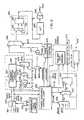
- FIG. 2is a block diagram of an example PLL circuit 200 which is implemented for such a synchronization.
- PLL circuit 200generates the sampling clock signal also.
- PLL circuit 200includes phase detector 210 , filter 220 , amplifier 230 , voltage controlled oscillator (VCO) 240 , and frequency divider 250 .
- Phase detector 210compares a time reference (e.g., VSYNC) received on line 102 and sampling clock (more accurately, a signal having a predetermined fraction of the sampling signal) received on line 251 .
- the two signalsare referred to as f 1 and f 2 for brevity.
- Phase detector 210provides on line 212 a signal having a difference of the frequencies of f 1 and f 2 .
- the signal on line 212may also include several harmonics of the difference frequency.
- Filter 220is generally designed as a low pass filter to eliminate undesirable components. When the frequencies f 1 and f 2 are close, but not equal, line 223 will carry a signal with the difference frequency.
- VCO 240is designed to generate a signal with a predetermined frequency. However, the frequency is altered depending on the voltage level received on line 234 .
- Amplifier 230amplifies the signal on line 223 to provide a desired level of voltage on line 234 to modify the frequency of VCO 240 .
- the voltage levelis generated so as to achieve a synchronization of the frequencies f 1 and f 2 .
- Frequency divider 250divides the frequency of clock signal received on line 245 by a factor of n. By choosing an appropriate value of n, analog signal data for each horizontal source scan line can be sampled a desired number of times. The signal on line 245 can be used for such a sampling.
- the reference frequencycan vary by a slight value from an average frequency during normal operating conditions.
- the reference frequencycan drift over a prolonged period of time due to, for example, temperature changes in the circuits generating the analog source image data.
- jittermay be present in both the reference signal and the clock signal generated by the analog PLL.
- the PLL of FIG. 2track the long term drifts while eliminating the jitters. This may be achieved by having a PLL circuit with low bandwidth (e.g., 100 to 1000 Hz). However, such a low bandwidth generally requires a capacitor having a large size, which may be hard to integrate into a relatively small-sized integrated circuits.
- Deviations of about 5 to 20 nano-seconds in time reference periodcan be common in a typical graphics environment. These deviations are usually more problematic for larger size display screens.
- a 640 ⁇ 480 size display screenhas a pixel processing period (i.e., average time to display each pixel) of 40 nano-seconds, while a large 1280 ⁇ 1080 size monitor can have a pixel processing period of about 8-9 nano-seconds.
- a deviation of 20 nano-secondsmay not have a perceptible impact on the display of a 640 ⁇ 480 screen due to the relatively larger pixel processing period, whereas the same amount of deviation can cause the display on the large monitor to be skewed by two pixels.
- Such a skew between linesis generally perceptible for the human eye and the resulting display quality may be unacceptable.
- the display qualityis further exacerbated if the number of such skews is larger.
- the display quality problemscan be ameliorated by a circuit which can track the time reference signal more closely. Therefore, what is needed is a circuit which tracks the time reference signal closely.
- the present inventionis directed to a clock recovery circuit implemented in a digital display unit.
- the digital display unitreceives an analog signal data and an associated time reference signal. Together, they represent an image to be displayed on a digital display screen usually provided in the digital display unit.
- the clock recovery circuitprovides a sampling clock based on the time reference signal.
- the sampling clockis used to sample the analog signal data, and the resulting pixel data is used to generate display signals on the display screen.
- the clock recovery circuitincludes a digital phase-locked loop (PLL).
- PLLdigital phase-locked loop
- the bandwidth of the PLLcan be instantaneously changed because of the digital implementation.
- the long term frequency and the temporary phase fluctuationsare tracked using different control loops. As a result, considerable flexibility is available to a designer to track the time reference signal.
- FIG. 1Ais a block diagram of an example display screen including several pixels arranged in horizontal rows;
- FIG. 1Bis a diagram of a signal shown in time domain illustrating an example time reference signal for an analog display data
- FIG. 2is a block diagram of a conventional PLL circuit implemented using analog components
- FIG. 3is a block diagram illustrating an embodiment of the clock recovery circuit of the present invention.
- FIG. 4is a block diagram of a digital PLL circuit illustrating independent loops for tracking frequency and phase
- FIG. 5is a block diagram of an example analog filter to filter undesirable frequency components from the output of the digital PLL
- FIG. 6is a block diagram of an example implementation of a digital PLL in one embodiment of the present invention.
- FIG. 7is a block diagram of an example graphics system implemented in accordance with the present invention.
- FIG. 8is a block diagram of an example digital display unit in accordance with the present invention.
- clock recovery circuit 300( FIG. 3 ) which includes digital PLL circuit 310 and analog filter 320 .
- the output of PLL circuit 310is coupled to the input of analog filter 320 .
- PLL circuit 310is implemented using digital components and signals.
- PLL circuit 310receives as input a time reference 301 and generates output signal 312 . While generating the output signal, PLL signal 310 attempts to synchronize the output signal 312 with time reference.
- Analog filter 320filters any undesirable spectral components in the output signal 312 and provides the filtered signal as input to PLL circuit on input 302 .
- PLL circuit 310is implemented using digital components and a designer is provided considerable flexibility to specify the degree or manner in which output signal 312 should track reference signal 301 . Due to such a flexibility, the bandwidth of PLL circuit 310 can be dynamically varied such that PLL circuit 310 can be made to adequately track reference signal 301 . Such a close tracking may prevent relative skewing among the display lines.
- PLL circuit 310As PLL circuit 310 is implemented using digital components, the circuit can be implemented to have a narrow bandwidth loop. Conventional analog PLLs may require large capacitors to implement an equivalent circuit. As already explained in the background section, integration of large capacitors into a semiconductor integrated circuit may be problematic.
- Analog filter 320can be conventional and is implemented using analog components in a known way.
- the output signal of analog signalcorresponds to the clock (e.g., sampling clock) synchronized with the time reference REF.
- the output signalis divided by K, where K may correspond to the number of samples taken per each horizontal source image line.
- clock recovery circuit 300Before describing the invention in great detail, it is useful to describe an example environment in which the invention can be implemented. The details of implementation and operation of clock recovery circuit 300 are then explained in detail.
- the inventioncan be implemented in any graphics system having a digital display unit.
- Such systemsinclude, without limitation, lap-top and desk-top personal computer systems (PCS), work-stations, special purpose computer systems, central purpose computer systems, and many others.
- PCSpersonal computer systems
- the inventionmay be implemented in hardware, software, firmware, or combination of the like.
- One or more embodiments which can use the clock recovery circuit of the present inventionis described in the co-pending application entitled, “A Method and Apparatus for Upscaling an Image”, which is referred to in the section above entitled “Related Applications.”
- FIG. 7is a block diagram of computer system 700 in which the present invention can be implemented.
- Computer system 700is only an example of a graphics system in which the present invention can be implemented.
- Computer system 700includes central processing unit (CPU) 710 , random access memory (RAM) 720 , one or more peripherals 730 , graphics controller 760 , and digital display unit 770 . All these components communicate over bus 750 , which can in reality include several physical buses connected by appropriate interfaces.
- Graphics controller 760generates analog image data and a corresponding reference signal, and provides both to digital display unit 200 .
- the analog image datacan be generated, for example, based on pixel data received from CPU 710 or from an external encoder (not shown).
- the analog image datais provided in RGB format and the reference signal includes the VSYNC and HSYNC signals well known in the art and explained above.
- the present inventioncan be implemented with analog image data and/or reference signals in other formats.
- analog image datacan include video signal data also with a corresponding time reference signal.
- Digital display unit 770can include a display screen having pixels as explained with reference to FIG. 1 A.
- Digital display unit 770includes a clock recovery circuit in accordance with the present invention. Using the clock recovery circuit, digital display unit 770 samples the analog signal data. The manner in which analog signal data is sampled if a sampling clock is provided to generate pixel data is well known in the art. Due to the clock recovery circuit of the present invention, digital display unit 770 may display an image corresponding to the analog signal data without a relative skewing of the lines.
- CPU 710 , RAM 720 and peripherals 730are conventional in one embodiment of the present invention.
- CPU 710can be, for example, a processor such as a Pentium Processor available from Intel Corporation.
- RAM 720represents the system/main memory for storing instructions and data. The instructions and data may be read from a peripheral device such a hard-disk.
- CPU 710executes the instructions using the data to provide various functions. As a part of executing the instructions, CPU 710 may send commands to graphics controller 710 , which generates analog display signal data in a known way. The manner in which an example embodiment of digital display unit 770 displays the image corresponding to the analog display signal will be explained in further detail below.
- digital display unit 770is implemented to operate with a computer system.
- Digital display unit 770can be in the form of a flat-panel monitor used in lap-top (note-book computers), a flat-monitor used in desk-top computers and workstations, among other forms.
- note-book computersnote-book computers
- flat-monitorused in desk-top computers and workstations, among other forms.
- FIG. 8is a block diagram of digital display unit 770 including analog-to-digital converter (ADC) 810 , upscaler 820 , panel interface 830 , clock generator circuit 850 , and display screen 100 .
- ADCanalog-to-digital converter
- the output line of ADC 810is coupled to the input line of upscaler 820 .
- the output line of upscaler 82is coupled to panel interface 831 .
- the output of panel interfaceis coupled to display screen 100 .
- Clock generator circuit 850is coupled to ADC 810 , upscaler 820 , panel interface 830 .
- ADC 810receives analog signal data on line 801 and a sampling clock signal on line 851 .
- ADC 810is conventional and samples the analog signal data according to the sampling clock signal.
- ADC 810provides the pixel data on line 812 to upscaler 820 .
- Upscaler 820uses the pixel data received on line 812 to optionally upscale the image represented by the pixel data.
- the imagemay be upscaled, for example, due to the lager size of display screen 100 .
- An embodiment of upscaler 820is described in co-pending application entitled, “A Method and Apparatus for Upscaling an Image”, which is referred to above in the section entitled “Related Applications.” In the co-pending application, upscaler 820 may be described as including the clock generation circuit 850 also.
- Clock generator 802generates the clock signals to ADC 810 , upscaler 820 and panel interface 830 .
- the individual clock signalsmay have different frequencies depending on the overall design.
- One or more the individual clock signalsmay be synchronized with time reference signal 802 by using the clock recovery circuit of the present invention.
- the manner in which different frequencies may be computed in one embodimentis also described in the co-pending application entitled, “A method and apparatus for upscaling an image.”
- time reference signal 802may correspond to HSYNC signal. In another embodiment, time reference signal 802 may correspond to VSYNC signal. However, it should be understood that time reference signal 802 may correspond to any other signal (including a combination of HSYNC and VSYNC) as suited in the specific environment.
- Display screen 100is explained in detail above.
- Display screen 100may be implemented using any digital screen technologies such as active/passive liquid crystal display (LCD) technologies.
- Panel interface 830is designed to generate display signals to display image on display screen 100 .
- Panel interface 830can be implemented in a known way to generate display signals to display screen 100 from the pixel data received from upscaler 820 .
- the clock recovery circuitsynchronizes (or attempts to synchronize) the generated clock with the time reference.
- PLL circuit 310will be explained first.
- analog filter 320will be explained.
- the time referencewill be assumed to include a HSYNC signal.
- the present inventioncan be practiced with other types of reference signals as well.
- FIG. 4is a block diagram illustrating internal blocks of an example embodiment of digital PLL circuit 310 .
- PLL circuit 310includes phase and frequency detector (PFD) 410 , frequency correction logic 420 , phase correction logic 430 , adders 440 and 450 , DTO 460 and DAC 470 .
- Phase correction logic 430 and frequency correction logic 420are connected to the output of PFD 410 .
- First adder 440is coupled to the output of frequency correction logic 420 .
- the output of first adderis coupled to second adder 450 .
- Second adderis also coupled to phase correction logic 430 .
- the output of second adder 450is coupled to DTO 460 .
- the output of DTOis in turn connected to digital to analog converter 470 .
- PFD 410compares the phase and frequency of time reference (HSYNC) signal and feedback signal.
- PFD 410is conventional and generates signals on EARLY and LATE lines depending on whether reference signal lags or leads the feedback signal.
- a pulseis generated according to the lead or lag and the duration of the pulse is proportional to the amount of lead or lag.
- the resynchronization processis achieved by having two separate blocks for correcting long term frequency drifts and phase jitters in the reference signal. By having two separate blocks, the designer may have more control over the resynchronization process.
- frequency correction logic 420is designed to correct the long term frequency drifts in the reference signal.
- the frequency driftsgenerally correspond to a change in the reference frequency, typically in the range of few hertz.
- the driftscan be a result of, for example, temperature fluctuations in the source system generating the source image.
- Frequency correction logic 420can be advantageously designed to track the reference signal over a prolonged period.
- Adder 440adds (subtracts) the frequency correction number provided by frequency correction logic 430 to Pnom frequency.
- Pnomcorresponds to an expected frequency of the sampling clock and is used during the frequency acquisition phase.
- Frequency acquisition phaserefers to a time duration during which the PLL loop is stabilizing and locking with the frequency of the reference signal. By providing the Pnom signal, the frequency acquisition period can be decreased.
- phase correction logic 430tracks phase fluctuations in the time reference.
- the output of phase correction logic 430represents the degree (or amount) of phase by which the clock signal being generated should be corrected due to the phase difference between time reference signal and feedback signal.
- the output of adder 440represents the current frequency of the loop.
- the outputs of phase correction logic 420 and adder 440are added using adder 450 .
- the output of adder 450represents the total of Pnom, frequency correction provided by frequency correction logic 420 , and phase correction provided by phase correction logic 430 . This total represents how far the phase in DTO 460 is advanced per DTO clock cycle. This total can change during each reference clock cycle.
- DTO 460is conventional and is also known as a phase accumulator. DTO 460 generates as an output a ramp signal having a fundamental frequency and other undesirable spectral components. The fundamental frequency represents the frequency of the clock which is synchronized with the time reference signal. The spectral frequencies are undesirable as they may contribute to clock jitter. Accordingly, these spectral frequencies are eliminated using the analog filter 320 .
- DAC 470converts the digital output of DTO into an analog form suited for processing by analog filter. Analog filter 320 is explained in further detail below. Before describing analog filter 320 in detail, an implementation of digital PLL circuit 310 is explained first.
- FIG. 6is a block diagram illustrating the design and operation of an example implementation of digital PLL circuit 310 .
- PLL circuit 310includes several components and signals interconnecting the components. Each component and signal will be explained in further detail below. Broadly, PLL circuit 310 will be described in three separate sections: (1) phase comparison, (2) frequency correction, and (3) phase correction.
- PFD 603has two output signal lines early 604 and late 605 indicating whether the feedback signal (FBACK) is early or late in phase in relation to time reference signal REF.
- PFD 603generates a pulse on early 604 , with the pulse having a duration which is proportional to the phase by which FBACK signal is early in comparison to REF signal.
- the pulse durationis measured in number of reference clock periods, where reference clock refers to a clock of which PLL circuit 310 operates.
- the pulses on early signal 604 and late signal 605will be generally referred to as an error pulse. Late signal 605 is similarly explained.
- PFD 603stops comparing REF and FBACK signal when STOP signal is asserted. When the comparison is stopped, both LATE and EARLY signals are unasserted.
- Charge/discharge control 650causes STOP signal to be asserted when the phase correction integrator can overflow.
- Comparison signal limiter 610causes STOP signal to be asserted when the phase difference exceeds a predetermined number.
- frequency correction control 620As to the frequency correction, frequency correction control 620 , multiplexor 630 , adder 627 and flip-flops 625 operate to provide the frequency correction.
- frequency correction control 620causes multiplexor 630 to select as output the value on input having number 2.
- A/S (Add/Subtract) signalis asserted to low, causing adder 627 to be set to a zero value by subtracting current accumulator value from itself.
- Frequency correction control 620then causes multiplexor 630 to select the Pnom value.
- Pnomcorresponds to an expected frequency of the sampling block being generated. Accordingly, the frequency acquisition period is reduced to a few cycles assuming that the REF signal has a frequency which is in slight deviation from the expected frequency. Without Pnom, frequency acquisition may take several cycles.
- frequency correction control 620causes Fdp value to be selected by multiplexor 630 .
- the Fdp valueis added/subtracted during each reference clock cycle there is the error pulse. Addition of the Fdp value causes the clock frequency to be increased and subtraction causes the clock frequency to be decreased.
- Fdp valueis provided from a register.
- the Fdp valuerepresents the loop bandwidth.
- a higher value of Fdpimplies that the PLL 310 will respond faster to changes and lower value implies that the PLL 310 will be more stable.
- the loop bandwidthcan also be changed instantaneously.
- Fdp valuecan be set fairly high, and it can be set to a low value once the loop stabilizes.
- Fdpcan be based on adaptive schemes which base individual Fdp values on the historical values of phase corrections. The manner in which Fdp value is set in one embodiment will be explained below.
- Frequency correction control 620enables FC-CE signal only during the length of the error pulse.
- the output of flip-flop 625represents the current average frequency of the clock being generated.
- phase correctionis broadly explained first.
- Charge/discharge control 650 along with the associated circuitrymay be viewed as a leaky integrator, but implemented in digital domain.
- the integratoris charged to a level using the PPDP value.
- the level to which it is chargeddepends on the duration of the error pulse length.
- the integratoris slowly discharged using the NPDP value.
- the NPDP valueis smaller in value in comparison to PPDP value and thus the discharge occurs during an extended period of time.
- the phase correctionis performed during the discharge cycles.
- the manner in which charging and discharging are performedis explained in further detail below. The manner in which NPDP and PPDP values are computed in one embodiment will then be explained.
- Charge/discharge control 650 , multiplexor 655 , adder 660 , and flip-flop 665together determine the charge on the integrator. It should be noted that flip-flop 665 (and other flip-flops described here) in reality includes several flip-flops, with each flip-flop storing one bit.
- the value in adder 660is cleared at the beginning of each time reference cycle (e.g., when a HSYNC pulse is received).
- the PPDP valueis added to adder 660 during each reference cycle (i.e., the internal clock of PLL) the error pulse is present.
- the integratoris determined to have overflown, and the integrator overflow detector 673 causes the STOP signal coupled to PFD 603 be asserted.
- flip-flop 665stores a value indicative of the charge on the integrator.
- phase correction of the clockis performed during the discharge phase.
- charge/discharge control 650causes NPDP value subtracted iteratively from accumulator 660 during each reference clock cycle.
- inactive REMINDER signalcauses NPDP value to be selected by multiplexor 652 .
- phase correction control 675provides PCORR signal so as to gate the output of AND logic 677 to adder 680 . Otherwise, PCORR signal is set at low signal level (logical value of 0) to set the output of AND logic 677 to zero.
- Phase correction control 675asserts the A/S input of adder 680 to cause the output of adder 677 to be added or subtracted. The value is added if the REF signal is ahead of FBACK signal and subtracted otherwise.
- the result after the subtractionmay be a negative number.
- the clock signalhas been over corrected.
- sign and zero crossing detector 670detects that the phase has been over corrected and causes charge/discharge control 650 to take corrective action.
- the negative numberis stored in flip-flop 674 .
- Charge/discharge control 650asserts REMINDER signal to 1 to cause multiplexor 652 to select the value stored in flip-flop 674 .
- the selected valueto provided to added 680 , which corrects the overcorrection.
- Phase correction control 675switches the value on the A/S input to adder 680 . That is, if previously the a 0 value is provided, a value of 1 is provided when forwarding the overcorrection parameter.
- DTO 460generates as an output a ramp signal representing phase of a fundamental frequency and other spectral components such as images resulting from the digital sampling.
- the fundamental frequencyrepresents the frequency of the clock which is synchronized with the time reference signal.
- the spectral componentsare undesirable as they may contribute to clock jitter.
- the remaining portion of the circuitis designed to eliminate these other frequencies while preserving the fundamental frequency.
- LUT 690is conventional and translates the phase output of DTO 460 to an amplitude value.
- the phase valuemay be converted to either a sine wave or a triangle as is also known well in the art.
- DAC 695converts the output of LUT 690 to an analog signal for suitable processing by analog filter 320 .
- An embodiment of analog filter 320is explained later.
- FIG. 6is merely an example implementation and it will be apparent to one skilled in the art to implement various modifications without departing from the scope and the spirit of the present invention.
- Pnom, NPDP and PPDP valueshave been described to be used. One example way of computing these parameters is explained.
- Qdtois DTO module, (i.e., 2**n, where n is the number of bits in DTO). It should be noted that Pnom isn't dependent on locking scheme. That is, the clock signal can be locked on HSYNC, VSYNC, or the like.
- Negative slope parameter(discharging) is derived from Ppdp.
- NPDPis usually close to Ppdp if loop is unlocked and several times smaller (8 . . . 16) if loop is locked (to minimize phase jumps).
- NpdpPpdp/Knpdp (4)
- Knpdp2 . . . 16
- Frequency correction parameteris dependent on locking scheme. It means amount of frequency adjustment per one Rclk phase tracking error.
- Vdivis vertical Hsync divider (1 . . . n). If Vdiv is 1, every Hsync is used for comparison. If Vdiv is 2, every other Hsync is used, etc. Vtotal is number of lines in the source frame if VSYNC locking is used.
- analog filter 320is designed to preserve the fundamental frequency generated by DTO while eliminating the other frequencies.
- Analog filter 320can be implemented using active or passive filters or using a phase-locked loop as is well-known in the art. An example embodiment of analog filter 320 is illustrated with reference to FIG. 5 .
- Analog filter 320is conventional and includes a DAC reconstruction filter 510 .
- Schmidt trigger 520slices the sine-wave in a known way to convert the sine-wave into digital signal (two level quantization).
- the PLL loopcomprising PFD 530 , charge pump 540 , loop filter 550 , VCO 560 , and divider 580 is designed to eliminate all the undesirable frequencies, while preserving the fundamental frequency.
- the value of N in divider 580is kept relatively small (at or below 8).
- VCO 560may be designed to generate sampling clock signal, which can be used to sample the analog signal data.
- Dividers 570 and 580may be used to shift the Vco frequency into the operating range of Vco 560 .
- the output of analog filter 320includes filtered signal with well-suppressed spurious spectral components.
Landscapes
- Engineering & Computer Science (AREA)
- Theoretical Computer Science (AREA)
- Physics & Mathematics (AREA)
- General Physics & Mathematics (AREA)
- Computer Hardware Design (AREA)
- General Engineering & Computer Science (AREA)
- Control Of Indicators Other Than Cathode Ray Tubes (AREA)
- Stabilization Of Oscillater, Synchronisation, Frequency Synthesizers (AREA)
Abstract
Description
Hor_Rcount−Th/Trclk (1)
where Trclk represents the clock period of reference clock and Th represents the horizontal period (time between two successive Hsync pulses).
Pnom=srs_htotal*Qdto/Hor_Rcount (2)
Here, Qdto is DTO module, (i.e., 2**n, where n is the number of bits in DTO). It should be noted that Pnom isn't dependent on locking scheme. That is, the clock signal can be locked on HSYNC, VSYNC, or the like.
Ppdp=Pnom/Kpdp (3)
Npdp=Ppdp/Knpdp (4)
Knpdp=2 . . . 16
Fdp=Pnom/(Kfdp*Vdiv*Hor_Rcount) (5a)
Fdp=Pnom/(Kfdp*Vtotal*Hor_Rcount) (5b)
Claims (18)
Priority Applications (4)
| Application Number | Priority Date | Filing Date | Title |
|---|---|---|---|
| US10/720,001USRE40859E1 (en) | 1997-02-24 | 2003-11-20 | Method and system for displaying an analog image by a digital display device |
| US11/408,669USRE41192E1 (en) | 1997-02-24 | 2006-04-21 | Method and system for displaying an analog image by a digital display device |
| US12/624,053USRE42615E1 (en) | 1997-02-24 | 2009-11-23 | Method and system for displaying an analog image by a digital display device |
| US13/168,832USRE43573E1 (en) | 1997-02-24 | 2011-06-24 | Method and system for displaying an analog image by a digital display device |
Applications Claiming Priority (3)
| Application Number | Priority Date | Filing Date | Title |
|---|---|---|---|
| US08/803,824US5796392A (en) | 1997-02-24 | 1997-02-24 | Method and apparatus for clock recovery in a digital display unit |
| US09/082,070US6320574B1 (en) | 1997-02-24 | 1998-05-20 | Circuit and method for generating pixel data elements from analog image data and associated synchronization signals |
| US10/720,001USRE40859E1 (en) | 1997-02-24 | 2003-11-20 | Method and system for displaying an analog image by a digital display device |
Related Parent Applications (2)
| Application Number | Title | Priority Date | Filing Date |
|---|---|---|---|
| US08/803,824ContinuationUS5796392A (en) | 1997-02-24 | 1997-02-24 | Method and apparatus for clock recovery in a digital display unit |
| US09/082,070ReissueUS6320574B1 (en) | 1997-02-24 | 1998-05-20 | Circuit and method for generating pixel data elements from analog image data and associated synchronization signals |
Related Child Applications (2)
| Application Number | Title | Priority Date | Filing Date |
|---|---|---|---|
| US09/082,070DivisionUS6320574B1 (en) | 1997-02-24 | 1998-05-20 | Circuit and method for generating pixel data elements from analog image data and associated synchronization signals |
| US11/408,669DivisionUSRE41192E1 (en) | 1997-02-24 | 2006-04-21 | Method and system for displaying an analog image by a digital display device |
Publications (1)
| Publication Number | Publication Date |
|---|---|
| USRE40859E1true USRE40859E1 (en) | 2009-07-21 |
Family
ID=25187534
Family Applications (6)
| Application Number | Title | Priority Date | Filing Date |
|---|---|---|---|
| US08/803,824Expired - LifetimeUS5796392A (en) | 1997-02-24 | 1997-02-24 | Method and apparatus for clock recovery in a digital display unit |
| US09/082,070CeasedUS6320574B1 (en) | 1997-02-24 | 1998-05-20 | Circuit and method for generating pixel data elements from analog image data and associated synchronization signals |
| US10/720,001Expired - LifetimeUSRE40859E1 (en) | 1997-02-24 | 2003-11-20 | Method and system for displaying an analog image by a digital display device |
| US11/408,669Expired - LifetimeUSRE41192E1 (en) | 1997-02-24 | 2006-04-21 | Method and system for displaying an analog image by a digital display device |
| US12/624,053CeasedUSRE42615E1 (en) | 1997-02-24 | 2009-11-23 | Method and system for displaying an analog image by a digital display device |
| US13/168,832Expired - LifetimeUSRE43573E1 (en) | 1997-02-24 | 2011-06-24 | Method and system for displaying an analog image by a digital display device |
Family Applications Before (2)
| Application Number | Title | Priority Date | Filing Date |
|---|---|---|---|
| US08/803,824Expired - LifetimeUS5796392A (en) | 1997-02-24 | 1997-02-24 | Method and apparatus for clock recovery in a digital display unit |
| US09/082,070CeasedUS6320574B1 (en) | 1997-02-24 | 1998-05-20 | Circuit and method for generating pixel data elements from analog image data and associated synchronization signals |
Family Applications After (3)
| Application Number | Title | Priority Date | Filing Date |
|---|---|---|---|
| US11/408,669Expired - LifetimeUSRE41192E1 (en) | 1997-02-24 | 2006-04-21 | Method and system for displaying an analog image by a digital display device |
| US12/624,053CeasedUSRE42615E1 (en) | 1997-02-24 | 2009-11-23 | Method and system for displaying an analog image by a digital display device |
| US13/168,832Expired - LifetimeUSRE43573E1 (en) | 1997-02-24 | 2011-06-24 | Method and system for displaying an analog image by a digital display device |
Country Status (5)
| Country | Link |
|---|---|
| US (6) | US5796392A (en) |
| EP (1) | EP0865019A3 (en) |
| JP (1) | JP2942750B2 (en) |
| KR (1) | KR100280041B1 (en) |
| TW (1) | TW424218B (en) |
Cited By (1)
| Publication number | Priority date | Publication date | Assignee | Title |
|---|---|---|---|---|
| USRE42615E1 (en)* | 1997-02-24 | 2011-08-16 | Genesis Microchip (Delaware) Inc. | Method and system for displaying an analog image by a digital display device |
Families Citing this family (50)
| Publication number | Priority date | Publication date | Assignee | Title |
|---|---|---|---|---|
| US5632045A (en)* | 1995-05-08 | 1997-05-27 | Chase Ergonomics, Inc. | Antivibration glove |
| KR200172661Y1 (en) | 1997-11-08 | 2000-03-02 | 윤종용 | A flat panel display apparatus having on screen display function |
| US6147668A (en)* | 1998-06-20 | 2000-11-14 | Genesis Microchip Corp. | Digital display unit of a computer system having an improved method and apparatus for sampling analog display signals |
| US6459426B1 (en)* | 1998-08-17 | 2002-10-01 | Genesis Microchip (Delaware) Inc. | Monolithic integrated circuit implemented in a digital display unit for generating digital data elements from an analog display signal received at high frequencies |
| TW522354B (en)* | 1998-08-31 | 2003-03-01 | Semiconductor Energy Lab | Display device and method of driving the same |
| US6232952B1 (en)* | 1998-09-30 | 2001-05-15 | Genesis Microchip Corp. | Method and apparatus for comparing frequently the phase of a target clock signal with the phase of a reference clock signal enabling quick synchronization |
| US6310618B1 (en) | 1998-11-13 | 2001-10-30 | Smartasic, Inc. | Clock generation for sampling analong video |
| JP2000232355A (en)* | 1999-02-09 | 2000-08-22 | Mitsubishi Electric Corp | Phase locked loop |
| KR100286233B1 (en)* | 1999-04-06 | 2001-03-15 | 임철호 | apparatus for interfacing timing information in digital display device |
| US6556250B1 (en)* | 1999-08-10 | 2003-04-29 | General Instrument Corporation | Method and apparatus for providing a timing signal with high frequency accuracy in video equipment for supporting an on-screen display in the absence of a video signal |
| KR100323666B1 (en)* | 1999-08-12 | 2002-02-07 | 구자홍 | Method and apparatus for compensating clock phase of monitor |
| US6272193B1 (en)* | 1999-09-27 | 2001-08-07 | Genesis Microchip Corp. | Receiver to recover data encoded in a serial communication channel |
| US6366174B1 (en) | 2000-02-21 | 2002-04-02 | Lexmark International, Inc. | Method and apparatus for providing a clock generation circuit for digitally controlled frequency or spread spectrum clocking |
| US6675306B1 (en)* | 2000-03-10 | 2004-01-06 | Ricoh Company Ltd. | Method and apparatus for phase-lock in a field programmable gate array (FPGA) |
| US6628276B1 (en)* | 2000-03-24 | 2003-09-30 | Stmicroelectronics, Inc. | System for high precision signal phase difference measurement |
| DE60126862T2 (en) | 2000-05-02 | 2007-10-31 | Thomson Licensing | Phase control for oscillators |
| US6573944B1 (en) | 2000-05-02 | 2003-06-03 | Thomson Licensing S.A. | Horizontal synchronization for digital television receiver |
| US20040183769A1 (en)* | 2000-09-08 | 2004-09-23 | Earl Schreyer | Graphics digitizer |
| US6912012B2 (en)* | 2001-07-20 | 2005-06-28 | Texas Instruments Incorporated | Video decoder having lock algorithm that distinguishes between a noisy television signal input and a video recorder signal |
| US6914951B2 (en)* | 2001-07-24 | 2005-07-05 | Hewlett-Packard Development Company, L.P. | Method and apparatus for a digital logic input signal noise filter |
| US6658043B2 (en) | 2001-10-26 | 2003-12-02 | Lexmark International, Inc. | Method and apparatus for providing multiple spread spectrum clock generator circuits with overlapping output frequencies |
| FR2832281B1 (en)* | 2001-11-09 | 2004-11-05 | St Microelectronics Sa | METHOD AND DEVICE FOR CONTROLLING THE OPERATION OF A VIDEO SYNCHRONIZATION CIRCUIT, PARTICULARLY FOR DETECTING THE NATURE OF THE VIDEO SOURCE, FOR EXAMPLE A VCR |
| US7072920B2 (en) | 2002-03-18 | 2006-07-04 | Genesis Microchip Inc. | Method and apparatus for digital frequency conversion |
| US7124153B2 (en) | 2002-03-18 | 2006-10-17 | Genesis Microchip Inc. | Frequency converter and methods of use thereof |
| US7358157B2 (en)* | 2002-03-27 | 2008-04-15 | Gsi Group Corporation | Method and system for high-speed precise laser trimming, scan lens system for use therein and electrical device produced thereby |
| US6951995B2 (en) | 2002-03-27 | 2005-10-04 | Gsi Lumonics Corp. | Method and system for high-speed, precise micromachining an array of devices |
| US7563695B2 (en)* | 2002-03-27 | 2009-07-21 | Gsi Group Corporation | Method and system for high-speed precise laser trimming and scan lens for use therein |
| US20060199354A1 (en)* | 2002-03-27 | 2006-09-07 | Bo Gu | Method and system for high-speed precise laser trimming and electrical device produced thereby |
| KR100826633B1 (en) | 2002-03-28 | 2008-05-02 | 지에스아이 루모닉스 코포레이션 | Method and system for high speed, precise micromachining of device array |
| US6674332B1 (en)* | 2002-09-06 | 2004-01-06 | Cypress Semiconductor, Corp. | Robust clock circuit architecture |
| JP2004247848A (en)* | 2003-02-12 | 2004-09-02 | Renesas Technology Corp | Communication equipment |
| JP3846469B2 (en)* | 2003-10-01 | 2006-11-15 | セイコーエプソン株式会社 | Projection display device and liquid crystal panel |
| US7154495B1 (en) | 2003-12-01 | 2006-12-26 | Analog Devices, Inc. | Analog interface structures and methods for digital displays |
| EP1698055A1 (en)* | 2003-12-15 | 2006-09-06 | Philips Intellectual Property & Standards GmbH | Circuit arrangement and method for locking onto and/or processing data, in particular audio, television and/or video data |
| CN100428205C (en)* | 2004-07-19 | 2008-10-22 | 明基电通股份有限公司 | Method for determining a digital image signal of a digital display |
| ATE504114T1 (en)* | 2005-04-18 | 2011-04-15 | Nxp Bv | CIRCUIT ARRANGEMENT, IN PARTICULAR PHASE CONTROL LOOP, AND CORRESPONDING METHOD |
| TWI268713B (en)* | 2005-04-21 | 2006-12-11 | Realtek Semiconductor Corp | Display device and display method thereof a display device comprising a zoom-scaling module and a digital display module |
| US7460113B2 (en)* | 2005-05-11 | 2008-12-02 | Ati Technologies Ulc | Digital pixel clock generation circuit and method employing independent clock |
| TWI285350B (en)* | 2005-07-29 | 2007-08-11 | Innolux Display Corp | A liquid crystal display |
| EP1938060A4 (en)* | 2005-09-21 | 2009-09-30 | Rjs Technology Inc | SYSTEM AND METHOD FOR A PICTURE SENSOR ELEMENT OR ARRAY WITH PHOTOMETRIC AND REAL-TIME MESSAGE CAPABILITIES |
| US7307562B2 (en)* | 2006-02-22 | 2007-12-11 | Analog Devices, Inc. | Spectrally-adjusted sampling methods and structures for digital displays |
| KR101237192B1 (en)* | 2006-03-06 | 2013-02-25 | 엘지디스플레이 주식회사 | Circuit of Recoverying Clock and Video Signal Receiver and Liquid Crystal Display System including the same |
| US20070215575A1 (en)* | 2006-03-15 | 2007-09-20 | Bo Gu | Method and system for high-speed, precise, laser-based modification of one or more electrical elements |
| US7975082B2 (en)* | 2007-07-12 | 2011-07-05 | Oracle America, Inc. | System and method to facilitate deterministic testing of data transfers between independent clock domains on a chip |
| US8441429B2 (en)* | 2008-10-14 | 2013-05-14 | Sharp Kabushiki Kaisha | Clock generation circuit, light source control circuit, and display device |
| DE112016001357T5 (en) | 2015-03-23 | 2017-12-07 | Microsemi SoC Corporation | Hybrid phase-locked loop with wide latching range |
| US9496879B1 (en)* | 2015-09-01 | 2016-11-15 | Qualcomm Incorporated | Multiphase clock data recovery for a 3-phase interface |
| EP3217557B1 (en) | 2016-03-11 | 2019-01-23 | Intel IP Corporation | Circuit, apparatus, digital phase locked loop, receiver, transceiver, mobile device, method and computer program to reduce noise in a phase signal |
| KR102720528B1 (en)* | 2019-03-27 | 2024-10-24 | 삼성디스플레이 주식회사 | Display device and driving method thereof |
| KR102788469B1 (en)* | 2022-11-16 | 2025-03-31 | 주식회사 로젠시스 | Transmitter for transmitting data in ultra high speed using pll |
Citations (105)
| Publication number | Priority date | Publication date | Assignee | Title |
|---|---|---|---|---|
| US4018990A (en) | 1975-02-13 | 1977-04-19 | Consolidated Video Systems, Inc. | Digital video synchronizer |
| JPS56137736A (en) | 1980-03-31 | 1981-10-27 | Anritsu Corp | Phase-synchronizing circuit |
| US4346407A (en) | 1980-06-16 | 1982-08-24 | Sanders Associates, Inc. | Apparatus for synchronization of a source of computer controlled video to another video source |
| US4432009A (en) | 1981-03-24 | 1984-02-14 | Rca Corporation | Video pre-filtering in phantom raster generating apparatus |
| US4488170A (en) | 1981-07-21 | 1984-12-11 | U.S. Philips Corporation | Synchronizing circuit for a television receiver |
| US4527145A (en) | 1981-09-15 | 1985-07-02 | Siemens Aktiengesellschaft | Method and apparatus for the digital control of the phase of the system clock of a digital signal processing system |
| US4554582A (en) | 1983-08-31 | 1985-11-19 | Rca Corporation | Apparatus for synchronizing a source of computer controlled video to another video source |
| US4590602A (en) | 1983-08-18 | 1986-05-20 | General Signal | Wide range clock recovery circuit |
| JPS61103369A (en) | 1984-10-26 | 1986-05-21 | Fuji Xerox Co Ltd | Optical reader |
| US4616259A (en) | 1984-04-27 | 1986-10-07 | General Electric Company | Instant phase correction in a phase-locked loop |
| JPS62146066A (en) | 1985-12-20 | 1987-06-30 | Matsushita Electric Ind Co Ltd | Image input/output device |
| US4686560A (en) | 1986-05-30 | 1987-08-11 | Rca Corporation | Phase locked loop system including analog and digital components |
| US4694327A (en) | 1986-03-28 | 1987-09-15 | Rca Corporation | Digital phase locked loop stabilization circuitry using a secondary digital phase locked loop |
| US4700217A (en) | 1986-08-05 | 1987-10-13 | Rca Corporation | Chrominance signal phase locked loop system for use in a digital television receiver having a line-locked clock signal |
| US4703340A (en) | 1986-05-02 | 1987-10-27 | Rca Corporation | Frequency division multiplexed analog to digital converter |
| JPS638983A (en) | 1986-06-30 | 1988-01-14 | Pfu Ltd | Enlarging/reducing system for input image |
| US4720745A (en) | 1983-06-22 | 1988-01-19 | Digivision, Inc. | Method and apparatus for enhancing video displays |
| JPS6314522A (en) | 1986-07-07 | 1988-01-21 | Toshiba Corp | Phase synchronizing circuit |
| JPS63188276A (en) | 1987-01-30 | 1988-08-03 | Matsushita Electric Ind Co Ltd | Image processing device |
| EP0299724A2 (en) | 1987-07-13 | 1989-01-18 | RCA Thomson Licensing Corporation | Digitally controlled phase locked loop system |
| WO1989005065A1 (en) | 1987-11-18 | 1989-06-01 | Bell Communications Research, Inc. | Digital phase locked loop with bounded jitter |
| JPH01169492A (en) | 1987-05-29 | 1989-07-04 | Commodore Electron Ltd | Highly resolving video output frame generation system |
| US4893319A (en) | 1988-12-19 | 1990-01-09 | Planar Systems, Inc. | Clock regeneration circuit employing digital phase locked loop |
| JPH0233271A (en) | 1988-07-22 | 1990-02-02 | Matsushita Electric Ind Co Ltd | Imaging device |
| US4906941A (en)* | 1988-05-25 | 1990-03-06 | Kabushiki Kaisha Toshiba | Digital phase locked loop circuit |
| JPH02135880A (en) | 1988-11-16 | 1990-05-24 | Matsushita Electric Ind Co Ltd | Imaging device |
| US4952125A (en) | 1988-04-06 | 1990-08-28 | Hitachi, Ltd. | Nonlubricated screw fluid machine |
| JPH02302173A (en) | 1989-05-17 | 1990-12-14 | Kyocera Corp | Image processing method |
| EP0405523A2 (en) | 1989-06-27 | 1991-01-02 | Sony Corporation | Charge pump circuit |
| US5005079A (en) | 1989-03-16 | 1991-04-02 | Sanyo Electric Co., Ltd. | Automatic frequency control circuit |
| US5010403A (en) | 1990-04-12 | 1991-04-23 | Tektronix, Inc. | Measurement of timebase jitter for component video |
| US5027212A (en) | 1989-12-06 | 1991-06-25 | Videologic Limited | Computer based video/graphics display system |
| US5029017A (en) | 1986-10-08 | 1991-07-02 | Konishiroku Photo Industry Co., Ltd. | Image processing apparatus capable of enlarging/reducing apparatus |
| US5086295A (en) | 1988-01-12 | 1992-02-04 | Boettcher Eric R | Apparatus for increasing color and spatial resolutions of a raster graphics system |
| US5101197A (en) | 1988-08-17 | 1992-03-31 | In Focus Systems, Inc. | Electronic transparency method and apparatus |
| EP0479508A2 (en) | 1990-09-29 | 1992-04-08 | Sharp Kabushiki Kaisha | Video display apparatus including display device having fixed two-dimensional pixel arrangement |
| EP0502600A2 (en) | 1991-03-05 | 1992-09-09 | nVIEW CORPORATION | Method and apparatus for displaying RGB and sync video without auxiliary frame storage memory |
| JPH0522277A (en) | 1991-07-15 | 1993-01-29 | Mitsubishi Electric Corp | Synchronous circuit |
| US5184091A (en) | 1991-06-04 | 1993-02-02 | Zenith Electronics Corporation | Circuit for phase locking an oscillator within any one of a plurality of frequency ranges |
| US5185603A (en) | 1990-07-13 | 1993-02-09 | Medin David L | Apparatus for synchronizing computer and video images to be simultaneously displayed on a monitor and method for performing same |
| JPH0583534A (en) | 1991-09-20 | 1993-04-02 | Brother Ind Ltd | Image enlarging device |
| US5202669A (en) | 1982-08-24 | 1993-04-13 | Sharp Kabushiki Kaisha | Display control device for superimposing data with a broadcast signal on a television screen |
| US5276515A (en) | 1991-09-26 | 1994-01-04 | Hitachi, Ltd. | Compatible wide aspect ratio receiver with spatial filtering for variable zoom |
| US5280345A (en) | 1991-04-04 | 1994-01-18 | Matsushita Electric Industrial Co., Ltd. | Jitter correction circuit for reducing jitter components of a luminance signal in video information compression |
| JPH0630247A (en) | 1992-07-07 | 1994-02-04 | Casio Comput Co Ltd | Image data magnification processor |
| JPH06205256A (en) | 1992-12-28 | 1994-07-22 | Canon Inc | Imaging device |
| US5335018A (en) | 1991-11-23 | 1994-08-02 | U.S. Philips Corporation | Digital phase-locked loop |
| US5335295A (en) | 1991-05-08 | 1994-08-02 | International Business Machines Corporation | System and method for scaling a digital image |
| EP0609843A1 (en) | 1993-02-01 | 1994-08-10 | Nec Corporation | Apparatus for driving liquid crystal display panel for different size images |
| EP0615222A1 (en) | 1993-03-10 | 1994-09-14 | Brooktree Corporation | Method to synchronize video modulation using a constant time base |
| US5349385A (en) | 1992-08-06 | 1994-09-20 | Florida Atlantic University | Adaptive scan converter |
| JPH06274611A (en) | 1993-03-24 | 1994-09-30 | Mitsubishi Electric Corp | Data conversion circuit |
| US5359366A (en) | 1991-12-27 | 1994-10-25 | Victor Company Of Japan, Ltd. | Time base correction apparatus |
| US5369376A (en)* | 1991-11-29 | 1994-11-29 | Standard Microsystems, Inc. | Programmable phase locked loop circuit and method of programming same |
| US5410357A (en) | 1993-04-12 | 1995-04-25 | The United States Of America As Represented By The Secretary Of The Navy | Scan converter and method |
| JPH07135592A (en) | 1993-11-11 | 1995-05-23 | Canon Inc | Imaging device |
| US5459766A (en) | 1993-04-05 | 1995-10-17 | U.S. Philips Corporation | Digital phase-locked loop |
| US5469223A (en) | 1993-10-13 | 1995-11-21 | Auravision Corporation | Shared line buffer architecture for a video processing circuit |
| JPH07334141A (en) | 1994-06-09 | 1995-12-22 | Sharp Corp | Multi-scan display device |
| US5497202A (en) | 1994-03-11 | 1996-03-05 | Samsung Electronics Co., Ltd. | Automatic digital frequency control circuit |
| US5515108A (en) | 1993-08-18 | 1996-05-07 | Samsung Electronics Corporation | Digital automatic frequency control method and circuit therefor |
| US5528307A (en) | 1991-07-18 | 1996-06-18 | Canon Kabushiki Kaisha | Clock generator |
| US5528305A (en)* | 1993-09-08 | 1996-06-18 | Samsung Electronics Co., Ltd. | Method for reducing empty sides of a wide screen and an apparatus thereof |
| JPH08172353A (en) | 1994-12-19 | 1996-07-02 | Hitachi Commun Syst Inc | Digital PLL circuit |
| US5535018A (en)* | 1991-10-15 | 1996-07-09 | Canon Kabushiki Kaisha | Information processing apparatus |
| US5534934A (en) | 1993-06-18 | 1996-07-09 | Hitachi, Ltd. | Television receiver capable of enlarging and compressing image |
| US5539473A (en) | 1994-03-31 | 1996-07-23 | Hewlett-Packard Company | Dot clock generation with minimal clock skew |
| US5574572A (en) | 1994-09-07 | 1996-11-12 | Harris Corporation | Video scaling method and device |
| US5574406A (en) | 1993-04-20 | 1996-11-12 | Rca Thomson Licensing Corporation | Phase lock loop with error measurement and correction in alternate periods |
| US5587742A (en) | 1995-08-25 | 1996-12-24 | Panasonic Technologies, Inc. | Flexible parallel processing architecture for video resizing |
| JPH08340254A (en) | 1995-06-12 | 1996-12-24 | Fujitsu Ltd | Frequency synthesizer |
| US5594467A (en) | 1989-12-06 | 1997-01-14 | Video Logic Ltd. | Computer based display system allowing mixing and windowing of graphics and video |
| US5600347A (en) | 1993-12-30 | 1997-02-04 | International Business Machines Corporation | Horizontal image expansion system for flat panel displays |
| US5623311A (en) | 1994-10-28 | 1997-04-22 | Matsushita Electric Corporation Of America | MPEG video decoder having a high bandwidth memory |
| US5646696A (en) | 1992-12-23 | 1997-07-08 | Intel Corporation | Continuously changing image scaling performed by incremented pixel interpolation |
| JPH09247574A (en) | 1996-03-06 | 1997-09-19 | Matsushita Electric Ind Co Ltd | Scan line converter |
| US5703618A (en) | 1995-11-22 | 1997-12-30 | Cirrus Logic, Inc. | Method and apparatus for upscaling video images when pixel data used for upscaling a source video image are unavailable |
| US5710573A (en) | 1995-05-04 | 1998-01-20 | Winbond Electronics Corp. | Scaled video output overlaid onto a computer graphics output |
| US5719633A (en) | 1994-12-20 | 1998-02-17 | Matsushita Electric Industrial Co., Ltd. | Video signal format conversion apparatus using simplified shifting and processing control |
| US5739808A (en) | 1994-10-28 | 1998-04-14 | Canon Kabushiki Kaisha | Display control method and apparatus |
| JPH10161365A (en) | 1996-12-04 | 1998-06-19 | Konica Corp | Correcting method of image density |
| US5781241A (en) | 1996-11-08 | 1998-07-14 | Chrontel, Inc. | Apparatus and method to convert computer graphics signals to television video signals with vertical and horizontal scaling requiring no frame buffers |
| US5790614A (en)* | 1993-06-09 | 1998-08-04 | Alcatel Network Systems, Inc. | Synchronized clock using a non-pullable reference oscillator |
| US5790096A (en) | 1996-09-03 | 1998-08-04 | Allus Technology Corporation | Automated flat panel display control system for accomodating broad range of video types and formats |
| US5838381A (en) | 1995-12-25 | 1998-11-17 | Hitachi, Ltd. | Image display apparatus capable of displaying personal computer signals and television signal by conversion into a signal of a higher number of pixels |
| US5841430A (en)* | 1992-01-30 | 1998-11-24 | Icl Personal Systems Oy | Digital video display having analog interface with clock and video signals synchronized to reduce image flicker |
| US5874937A (en) | 1995-10-20 | 1999-02-23 | Seiko Epson Corporation | Method and apparatus for scaling up and down a video image |
| US5909205A (en) | 1995-11-30 | 1999-06-01 | Hitachi, Ltd. | Liquid crystal display control device |
| US5926174A (en) | 1995-05-29 | 1999-07-20 | Canon Kabushiki Kaisha | Display apparatus capable of image display for video signals of plural kinds |
| US5940061A (en) | 1995-09-22 | 1999-08-17 | Kabushiki Kaisha Toshiba | Liquid-crystal display |
| US5953074A (en) | 1996-11-18 | 1999-09-14 | Sage, Inc. | Video adapter circuit for detection of analog video scanning formats |
| US6002810A (en) | 1995-04-14 | 1999-12-14 | Hitachi, Ltd. | Resolution conversion system and method |
| US6002446A (en) | 1997-02-24 | 1999-12-14 | Paradise Electronics, Inc. | Method and apparatus for upscaling an image |
| US6037925A (en) | 1996-04-17 | 2000-03-14 | Samsung Electronics Co., Ltd. | Video signal converting apparatus and a display device having the same |
| US6046737A (en)* | 1996-02-14 | 2000-04-04 | Fujitsu Limited | Display device with a display mode identification function and a display mode identification method |
| US6067071A (en) | 1996-06-27 | 2000-05-23 | Cirrus Logic, Inc. | Method and apparatus for expanding graphics images for LCD panels |
| US6078361A (en) | 1996-11-18 | 2000-06-20 | Sage, Inc | Video adapter circuit for conversion of an analog video signal to a digital display image |
| US6078317A (en)* | 1994-10-12 | 2000-06-20 | Canon Kabushiki Kaisha | Display device, and display control method and apparatus therefor |
| US6115020A (en) | 1996-03-29 | 2000-09-05 | Fujitsu Limited | Liquid crystal display device and display method of the same |
| US6144355A (en)* | 1995-10-16 | 2000-11-07 | Kabushiki Kaisha Toshiba | Display device including a phase adjuster |
| US6195079B1 (en) | 1996-11-18 | 2001-02-27 | Sage, Inc. | On-screen user interface for a video adapter circuit |
| US6215467B1 (en) | 1995-04-27 | 2001-04-10 | Canon Kabushiki Kaisha | Display control apparatus and method and display apparatus |
| US6219023B1 (en) | 1996-07-05 | 2001-04-17 | Samsung Electronics Co., Ltd. | Video signal converting apparatus with display mode conversion and a display device having the same |
| US6310602B1 (en) | 1993-09-30 | 2001-10-30 | Hitachi, Ltd. | Liquid crystal display system capable of reducing and enlarging resolution of input display data |
| US6310618B1 (en) | 1998-11-13 | 2001-10-30 | Smartasic, Inc. | Clock generation for sampling analong video |
Family Cites Families (15)
| Publication number | Priority date | Publication date | Assignee | Title |
|---|---|---|---|---|
| JPS6111074A (en) | 1984-06-27 | 1986-01-18 | 有限会社 大東製作所 | Line drawing device |
| JPS61212539A (en) | 1985-03-15 | 1986-09-20 | Daicel Chem Ind Ltd | Method of optical resolution of alpha-chloropropionic acid |
| JPS638983Y2 (en) | 1985-12-28 | 1988-03-17 | ||
| JPS62146066U (en) | 1986-03-10 | 1987-09-14 | ||
| JPH0630247B2 (en) | 1986-05-31 | 1994-04-20 | 東芝電池株式会社 | Method for manufacturing non-aqueous solvent secondary battery |
| JPH0522277Y2 (en) | 1987-04-24 | 1993-06-08 | ||
| JPH0535908Y2 (en) | 1987-05-27 | 1993-09-10 | ||
| JPH01169492U (en) | 1988-05-20 | 1989-11-29 | ||
| JPH0630247Y2 (en) | 1989-12-25 | 1994-08-17 | 日本碍子株式会社 | Filter cloth joint for pressure dehydrator |
| GB9219596D0 (en) | 1992-09-16 | 1992-10-28 | Videologic Ltd | Improvments relating to computer graphics and video systems |
| US5331346A (en) | 1992-10-07 | 1994-07-19 | Panasonic Technologies, Inc. | Approximating sample rate conversion system |
| KR0123919B1 (en) | 1994-02-17 | 1997-11-26 | 구자홍 | Encoder Flicker Reduction Device |
| US5621767A (en)* | 1994-09-30 | 1997-04-15 | Hughes Electronics | Method and device for locking on a carrier signal by dividing frequency band into segments for segment signal quality determination and selecting better signal quality segment |
| JPH10161635A (en) | 1996-12-03 | 1998-06-19 | Sega Enterp Ltd | Image synthesis device and image decoding device |
| US5796392A (en)* | 1997-02-24 | 1998-08-18 | Paradise Electronics, Inc. | Method and apparatus for clock recovery in a digital display unit |
- 1997
- 1997-02-24USUS08/803,824patent/US5796392A/ennot_activeExpired - Lifetime
- 1998
- 1998-01-19TWTW087100653Apatent/TW424218B/ennot_activeIP Right Cessation
- 1998-02-17EPEP98301141Apatent/EP0865019A3/ennot_activeWithdrawn
- 1998-02-23KRKR1019980005539Apatent/KR100280041B1/ennot_activeExpired - Fee Related
- 1998-02-24JPJP10042414Apatent/JP2942750B2/ennot_activeExpired - Fee Related
- 1998-05-20USUS09/082,070patent/US6320574B1/ennot_activeCeased
- 2003
- 2003-11-20USUS10/720,001patent/USRE40859E1/ennot_activeExpired - Lifetime
- 2006
- 2006-04-21USUS11/408,669patent/USRE41192E1/ennot_activeExpired - Lifetime
- 2009
- 2009-11-23USUS12/624,053patent/USRE42615E1/ennot_activeCeased
- 2011
- 2011-06-24USUS13/168,832patent/USRE43573E1/ennot_activeExpired - Lifetime
Patent Citations (114)
| Publication number | Priority date | Publication date | Assignee | Title |
|---|---|---|---|---|
| US4018990A (en) | 1975-02-13 | 1977-04-19 | Consolidated Video Systems, Inc. | Digital video synchronizer |
| JPS56137736A (en) | 1980-03-31 | 1981-10-27 | Anritsu Corp | Phase-synchronizing circuit |
| US4346407A (en) | 1980-06-16 | 1982-08-24 | Sanders Associates, Inc. | Apparatus for synchronization of a source of computer controlled video to another video source |
| US4432009A (en) | 1981-03-24 | 1984-02-14 | Rca Corporation | Video pre-filtering in phantom raster generating apparatus |
| US4462024A (en) | 1981-03-24 | 1984-07-24 | Rca Corporation | Memory scanning address generator |
| US4488170A (en) | 1981-07-21 | 1984-12-11 | U.S. Philips Corporation | Synchronizing circuit for a television receiver |
| US4527145A (en) | 1981-09-15 | 1985-07-02 | Siemens Aktiengesellschaft | Method and apparatus for the digital control of the phase of the system clock of a digital signal processing system |
| US5202669A (en) | 1982-08-24 | 1993-04-13 | Sharp Kabushiki Kaisha | Display control device for superimposing data with a broadcast signal on a television screen |
| US4720745A (en) | 1983-06-22 | 1988-01-19 | Digivision, Inc. | Method and apparatus for enhancing video displays |
| US4590602A (en) | 1983-08-18 | 1986-05-20 | General Signal | Wide range clock recovery circuit |
| US4554582A (en) | 1983-08-31 | 1985-11-19 | Rca Corporation | Apparatus for synchronizing a source of computer controlled video to another video source |
| US4616259A (en) | 1984-04-27 | 1986-10-07 | General Electric Company | Instant phase correction in a phase-locked loop |
| JPS61103369A (en) | 1984-10-26 | 1986-05-21 | Fuji Xerox Co Ltd | Optical reader |
| JPS62146066A (en) | 1985-12-20 | 1987-06-30 | Matsushita Electric Ind Co Ltd | Image input/output device |
| US4694327A (en) | 1986-03-28 | 1987-09-15 | Rca Corporation | Digital phase locked loop stabilization circuitry using a secondary digital phase locked loop |
| US4703340A (en) | 1986-05-02 | 1987-10-27 | Rca Corporation | Frequency division multiplexed analog to digital converter |
| US4686560A (en) | 1986-05-30 | 1987-08-11 | Rca Corporation | Phase locked loop system including analog and digital components |
| JPS638983A (en) | 1986-06-30 | 1988-01-14 | Pfu Ltd | Enlarging/reducing system for input image |
| JPS6314522A (en) | 1986-07-07 | 1988-01-21 | Toshiba Corp | Phase synchronizing circuit |
| US4700217A (en) | 1986-08-05 | 1987-10-13 | Rca Corporation | Chrominance signal phase locked loop system for use in a digital television receiver having a line-locked clock signal |
| US5029017A (en) | 1986-10-08 | 1991-07-02 | Konishiroku Photo Industry Co., Ltd. | Image processing apparatus capable of enlarging/reducing apparatus |
| JPS63188276A (en) | 1987-01-30 | 1988-08-03 | Matsushita Electric Ind Co Ltd | Image processing device |
| JPH01169492A (en) | 1987-05-29 | 1989-07-04 | Commodore Electron Ltd | Highly resolving video output frame generation system |
| EP0299724A2 (en) | 1987-07-13 | 1989-01-18 | RCA Thomson Licensing Corporation | Digitally controlled phase locked loop system |
| US4802009A (en) | 1987-07-13 | 1989-01-31 | Rca Licensing Corporation | Digitally controlled phase locked loop system |
| WO1989005065A1 (en) | 1987-11-18 | 1989-06-01 | Bell Communications Research, Inc. | Digital phase locked loop with bounded jitter |
| US5086295A (en) | 1988-01-12 | 1992-02-04 | Boettcher Eric R | Apparatus for increasing color and spatial resolutions of a raster graphics system |
| US4952125A (en) | 1988-04-06 | 1990-08-28 | Hitachi, Ltd. | Nonlubricated screw fluid machine |
| US4906941A (en)* | 1988-05-25 | 1990-03-06 | Kabushiki Kaisha Toshiba | Digital phase locked loop circuit |
| JPH0233271A (en) | 1988-07-22 | 1990-02-02 | Matsushita Electric Ind Co Ltd | Imaging device |
| US5101197A (en) | 1988-08-17 | 1992-03-31 | In Focus Systems, Inc. | Electronic transparency method and apparatus |
| JPH02135880A (en) | 1988-11-16 | 1990-05-24 | Matsushita Electric Ind Co Ltd | Imaging device |
| US4893319A (en) | 1988-12-19 | 1990-01-09 | Planar Systems, Inc. | Clock regeneration circuit employing digital phase locked loop |
| US5005079A (en) | 1989-03-16 | 1991-04-02 | Sanyo Electric Co., Ltd. | Automatic frequency control circuit |
| JPH02302173A (en) | 1989-05-17 | 1990-12-14 | Kyocera Corp | Image processing method |
| EP0405523A2 (en) | 1989-06-27 | 1991-01-02 | Sony Corporation | Charge pump circuit |
| US5027212A (en) | 1989-12-06 | 1991-06-25 | Videologic Limited | Computer based video/graphics display system |
| US5594467A (en) | 1989-12-06 | 1997-01-14 | Video Logic Ltd. | Computer based display system allowing mixing and windowing of graphics and video |
| US5010403A (en) | 1990-04-12 | 1991-04-23 | Tektronix, Inc. | Measurement of timebase jitter for component video |
| US5185603A (en) | 1990-07-13 | 1993-02-09 | Medin David L | Apparatus for synchronizing computer and video images to be simultaneously displayed on a monitor and method for performing same |
| EP0479508A2 (en) | 1990-09-29 | 1992-04-08 | Sharp Kabushiki Kaisha | Video display apparatus including display device having fixed two-dimensional pixel arrangement |
| US5227882A (en) | 1990-09-29 | 1993-07-13 | Sharp Kabushiki Kaisha | Video display apparatus including display device having fixed two-dimensional pixel arrangement |
| JPH04138494A (en) | 1990-09-29 | 1992-05-12 | Sharp Corp | Video display device |
| EP0502600A2 (en) | 1991-03-05 | 1992-09-09 | nVIEW CORPORATION | Method and apparatus for displaying RGB and sync video without auxiliary frame storage memory |
| JPH05150219A (en) | 1991-03-05 | 1993-06-18 | N View Corp | Method and apparatus for displaying rgb and synchronized video signal without auxiliary frame memory |
| US5280345A (en) | 1991-04-04 | 1994-01-18 | Matsushita Electric Industrial Co., Ltd. | Jitter correction circuit for reducing jitter components of a luminance signal in video information compression |
| US5335295A (en) | 1991-05-08 | 1994-08-02 | International Business Machines Corporation | System and method for scaling a digital image |
| US5184091A (en) | 1991-06-04 | 1993-02-02 | Zenith Electronics Corporation | Circuit for phase locking an oscillator within any one of a plurality of frequency ranges |
| JPH0522277A (en) | 1991-07-15 | 1993-01-29 | Mitsubishi Electric Corp | Synchronous circuit |
| US5528307A (en) | 1991-07-18 | 1996-06-18 | Canon Kabushiki Kaisha | Clock generator |
| JPH0583534A (en) | 1991-09-20 | 1993-04-02 | Brother Ind Ltd | Image enlarging device |
| US5276515A (en) | 1991-09-26 | 1994-01-04 | Hitachi, Ltd. | Compatible wide aspect ratio receiver with spatial filtering for variable zoom |
| US5535018A (en)* | 1991-10-15 | 1996-07-09 | Canon Kabushiki Kaisha | Information processing apparatus |
| US5335018A (en) | 1991-11-23 | 1994-08-02 | U.S. Philips Corporation | Digital phase-locked loop |
| US5369376A (en)* | 1991-11-29 | 1994-11-29 | Standard Microsystems, Inc. | Programmable phase locked loop circuit and method of programming same |
| US5359366A (en) | 1991-12-27 | 1994-10-25 | Victor Company Of Japan, Ltd. | Time base correction apparatus |
| US5841430A (en)* | 1992-01-30 | 1998-11-24 | Icl Personal Systems Oy | Digital video display having analog interface with clock and video signals synchronized to reduce image flicker |
| JPH0630247A (en) | 1992-07-07 | 1994-02-04 | Casio Comput Co Ltd | Image data magnification processor |
| US5349385A (en) | 1992-08-06 | 1994-09-20 | Florida Atlantic University | Adaptive scan converter |
| US5646696A (en) | 1992-12-23 | 1997-07-08 | Intel Corporation | Continuously changing image scaling performed by incremented pixel interpolation |
| JPH06205256A (en) | 1992-12-28 | 1994-07-22 | Canon Inc | Imaging device |
| EP0609843A1 (en) | 1993-02-01 | 1994-08-10 | Nec Corporation | Apparatus for driving liquid crystal display panel for different size images |
| US5406308A (en)* | 1993-02-01 | 1995-04-11 | Nec Corporation | Apparatus for driving liquid crystal display panel for different size images |
| EP0615222A1 (en) | 1993-03-10 | 1994-09-14 | Brooktree Corporation | Method to synchronize video modulation using a constant time base |
| US5638131A (en)* | 1993-03-10 | 1997-06-10 | Brooktree Corporation | Method to synchronize video modulation using a constant time base |
| JPH06274611A (en) | 1993-03-24 | 1994-09-30 | Mitsubishi Electric Corp | Data conversion circuit |
| US5459766A (en) | 1993-04-05 | 1995-10-17 | U.S. Philips Corporation | Digital phase-locked loop |
| US5410357A (en) | 1993-04-12 | 1995-04-25 | The United States Of America As Represented By The Secretary Of The Navy | Scan converter and method |
| US5574406A (en) | 1993-04-20 | 1996-11-12 | Rca Thomson Licensing Corporation | Phase lock loop with error measurement and correction in alternate periods |
| US5790614A (en)* | 1993-06-09 | 1998-08-04 | Alcatel Network Systems, Inc. | Synchronized clock using a non-pullable reference oscillator |
| US5534934A (en) | 1993-06-18 | 1996-07-09 | Hitachi, Ltd. | Television receiver capable of enlarging and compressing image |
| US5515108A (en) | 1993-08-18 | 1996-05-07 | Samsung Electronics Corporation | Digital automatic frequency control method and circuit therefor |
| US5528305A (en)* | 1993-09-08 | 1996-06-18 | Samsung Electronics Co., Ltd. | Method for reducing empty sides of a wide screen and an apparatus thereof |
| US6310602B1 (en) | 1993-09-30 | 2001-10-30 | Hitachi, Ltd. | Liquid crystal display system capable of reducing and enlarging resolution of input display data |
| US5469223A (en) | 1993-10-13 | 1995-11-21 | Auravision Corporation | Shared line buffer architecture for a video processing circuit |
| JPH07135592A (en) | 1993-11-11 | 1995-05-23 | Canon Inc | Imaging device |
| US5600347A (en) | 1993-12-30 | 1997-02-04 | International Business Machines Corporation | Horizontal image expansion system for flat panel displays |
| US5497202A (en) | 1994-03-11 | 1996-03-05 | Samsung Electronics Co., Ltd. | Automatic digital frequency control circuit |
| US5539473A (en) | 1994-03-31 | 1996-07-23 | Hewlett-Packard Company | Dot clock generation with minimal clock skew |
| JPH07334141A (en) | 1994-06-09 | 1995-12-22 | Sharp Corp | Multi-scan display device |
| US5574572A (en) | 1994-09-07 | 1996-11-12 | Harris Corporation | Video scaling method and device |
| US6078317A (en)* | 1994-10-12 | 2000-06-20 | Canon Kabushiki Kaisha | Display device, and display control method and apparatus therefor |
| US5623311A (en) | 1994-10-28 | 1997-04-22 | Matsushita Electric Corporation Of America | MPEG video decoder having a high bandwidth memory |
| US5739808A (en) | 1994-10-28 | 1998-04-14 | Canon Kabushiki Kaisha | Display control method and apparatus |
| JPH08172353A (en) | 1994-12-19 | 1996-07-02 | Hitachi Commun Syst Inc | Digital PLL circuit |
| US5719633A (en) | 1994-12-20 | 1998-02-17 | Matsushita Electric Industrial Co., Ltd. | Video signal format conversion apparatus using simplified shifting and processing control |
| US6002810A (en) | 1995-04-14 | 1999-12-14 | Hitachi, Ltd. | Resolution conversion system and method |
| US6215467B1 (en) | 1995-04-27 | 2001-04-10 | Canon Kabushiki Kaisha | Display control apparatus and method and display apparatus |
| US5710573A (en) | 1995-05-04 | 1998-01-20 | Winbond Electronics Corp. | Scaled video output overlaid onto a computer graphics output |
| US5926174A (en) | 1995-05-29 | 1999-07-20 | Canon Kabushiki Kaisha | Display apparatus capable of image display for video signals of plural kinds |
| JPH08340254A (en) | 1995-06-12 | 1996-12-24 | Fujitsu Ltd | Frequency synthesizer |
| US5587742A (en) | 1995-08-25 | 1996-12-24 | Panasonic Technologies, Inc. | Flexible parallel processing architecture for video resizing |
| US5940061A (en) | 1995-09-22 | 1999-08-17 | Kabushiki Kaisha Toshiba | Liquid-crystal display |
| US6144355A (en)* | 1995-10-16 | 2000-11-07 | Kabushiki Kaisha Toshiba | Display device including a phase adjuster |
| US5874937A (en) | 1995-10-20 | 1999-02-23 | Seiko Epson Corporation | Method and apparatus for scaling up and down a video image |
| US5703618A (en) | 1995-11-22 | 1997-12-30 | Cirrus Logic, Inc. | Method and apparatus for upscaling video images when pixel data used for upscaling a source video image are unavailable |
| US6121947A (en) | 1995-11-30 | 2000-09-19 | Hitachi, Ltd. | Liquid crystal display Control device |
| US5909205A (en) | 1995-11-30 | 1999-06-01 | Hitachi, Ltd. | Liquid crystal display control device |
| US5838381A (en) | 1995-12-25 | 1998-11-17 | Hitachi, Ltd. | Image display apparatus capable of displaying personal computer signals and television signal by conversion into a signal of a higher number of pixels |
| US6046737A (en)* | 1996-02-14 | 2000-04-04 | Fujitsu Limited | Display device with a display mode identification function and a display mode identification method |
| JPH09247574A (en) | 1996-03-06 | 1997-09-19 | Matsushita Electric Ind Co Ltd | Scan line converter |
| US6115020A (en) | 1996-03-29 | 2000-09-05 | Fujitsu Limited | Liquid crystal display device and display method of the same |
| US6037925A (en) | 1996-04-17 | 2000-03-14 | Samsung Electronics Co., Ltd. | Video signal converting apparatus and a display device having the same |
| US6067071A (en) | 1996-06-27 | 2000-05-23 | Cirrus Logic, Inc. | Method and apparatus for expanding graphics images for LCD panels |
| US6219023B1 (en) | 1996-07-05 | 2001-04-17 | Samsung Electronics Co., Ltd. | Video signal converting apparatus with display mode conversion and a display device having the same |
| US5790096A (en) | 1996-09-03 | 1998-08-04 | Allus Technology Corporation | Automated flat panel display control system for accomodating broad range of video types and formats |
| US5914753A (en) | 1996-11-08 | 1999-06-22 | Chrontel, Inc. | Apparatus and method to convert computer graphics signals to television video signals with vertical and horizontal scaling requiring no frame buffers |
| US5781241A (en) | 1996-11-08 | 1998-07-14 | Chrontel, Inc. | Apparatus and method to convert computer graphics signals to television video signals with vertical and horizontal scaling requiring no frame buffers |
| US6078361A (en) | 1996-11-18 | 2000-06-20 | Sage, Inc | Video adapter circuit for conversion of an analog video signal to a digital display image |
| US5953074A (en) | 1996-11-18 | 1999-09-14 | Sage, Inc. | Video adapter circuit for detection of analog video scanning formats |
| US6195079B1 (en) | 1996-11-18 | 2001-02-27 | Sage, Inc. | On-screen user interface for a video adapter circuit |
| JPH10161365A (en) | 1996-12-04 | 1998-06-19 | Konica Corp | Correcting method of image density |
| US6002446A (en) | 1997-02-24 | 1999-12-14 | Paradise Electronics, Inc. | Method and apparatus for upscaling an image |
| US6310618B1 (en) | 1998-11-13 | 2001-10-30 | Smartasic, Inc. | Clock generation for sampling analong video |
Non-Patent Citations (12)
| Title |
|---|
| "Combined Digital Zooming and Digital Effects System Utilizing CCD Signal Characteristics", IEEE Transactions on Consumer Electronics, vol. 39, No. 3, Aug. 1993, pp. 398-406, Palk et al. |
| "Fast Prototyping of Video Interface Controller for AML CD System", Proceedings of the 4th Asian Symposium on Information Display, pp. 195-198, Cheng et al. Feb. 13, 1997. |
| "Hardware Accelerators for Bitonal Image Processing" Digital Technical Journal, vol. 3 No. 4, Fall 1991, pp. 1-36, Payson et al., Fall 1991. |
| "High Speed Image Scaling for Integrated Document Management", Second ACM-SIGOA Conference on Office Information Systems, vol. 5, Nos. 1-2, pp. 36-45, Tabata et al., Jun. 25, 1984. |
| "High-Speed Rotation of Digital Images by Raster Scanning and Table-Lockup Operations", Systems and Computers in Japan, vol. 17, No. 11, pp. 76-87, Tabata et al., 1986. |
| "Initial Determination Concerning Violation of Section 337 and Recommended Determination on Issues Concerning Permanent Relief", Publication Versions, United States International Trade Commission, Washing, D.C., Apr. 14, 2004. |
| "Initial Determination on Remand Concerning Violation of Section 337", Public Version, United States International Trade Commission, Washington, D.C., May 20, 2004. |
| "Low Cost Video Scaler and Gray Scale Integrator", IEEE Tranactions on Biomedical Engineering, vol. 41, No. 7, pp. 698-703, Pietras & Bolanowski Jul. 1, 1994. |
| D'Alto et al publication: A Highly Integrated Scanning Rate Converter for IQTV, 1994 IEEE-Jun. 27, 1994. |
| Development of 13.3 In. Super TFT-LCD Monitor, SID International Symposium, Digest of Technical Papers, pp. 414-417, Kasai et al., May 1996. |
| Ferraro: Programmer's Guide to the EGA and VGA Cards, 1988 p. 32, D'Alto V., et al. |
| Katsumata Article: "Development of Picture Converting System Applying an NTSC Signal to a Wide Aspect Display" K. Katsumata, et al., IEEE Trans. on CE; vol. 38 No. 3, pp. 303-312, Aug. 1992. |
Cited By (1)
| Publication number | Priority date | Publication date | Assignee | Title |
|---|---|---|---|---|
| USRE42615E1 (en)* | 1997-02-24 | 2011-08-16 | Genesis Microchip (Delaware) Inc. | Method and system for displaying an analog image by a digital display device |
Also Published As
| Publication number | Publication date |
|---|---|
| JP2942750B2 (en) | 1999-08-30 |
| USRE42615E1 (en) | 2011-08-16 |
| US6320574B1 (en) | 2001-11-20 |
| KR100280041B1 (en) | 2001-02-01 |
| JPH10285022A (en) | 1998-10-23 |
| EP0865019A2 (en) | 1998-09-16 |
| KR19980071593A (en) | 1998-10-26 |
| US5796392A (en) | 1998-08-18 |
| EP0865019A3 (en) | 1999-06-09 |
| USRE43573E1 (en) | 2012-08-14 |
| TW424218B (en) | 2001-03-01 |
| USRE41192E1 (en) | 2010-04-06 |
Similar Documents
| Publication | Publication Date | Title |
|---|---|---|
| USRE40859E1 (en) | Method and system for displaying an analog image by a digital display device | |
| US5821818A (en) | Phase locked loop ciruit for a liquid crystal display | |
| US7142187B1 (en) | Liquid crystal display driving scaler capable of reducing electromagnetic interference | |
| US7498852B1 (en) | Phase error correction circuit for a high speed frequency synthesizer | |
| US6700570B2 (en) | Image display apparatus | |
| US6232952B1 (en) | Method and apparatus for comparing frequently the phase of a target clock signal with the phase of a reference clock signal enabling quick synchronization | |
| US20050134337A1 (en) | Clock signal distribution with reduced parasitic loading effects | |
| US6285402B1 (en) | Device and method for converting scanning | |
| US20020167365A1 (en) | Intelligent phase lock loop | |
| US5686968A (en) | Synchronizing signal generation circuit | |
| US5959691A (en) | Digital display apparatus having image size adjustment | |
| US20090161809A1 (en) | Method and Apparatus for Variable Frame Rate | |
| US5479073A (en) | Dot clock generator for liquid crystal display device | |
| US6392641B1 (en) | PLL circuit for digital display apparatus | |
| US6449017B1 (en) | RGB self-alignment and intelligent clock recovery | |
| US20050078126A1 (en) | Method and apparatus for scaling image in horizontal and vertical directions | |
| US6411267B1 (en) | Monitor adjustment by data manipulation | |
| US6157376A (en) | Method and apparatus for generating a target clock signal having a frequency of X/Y times the frequency of a reference clock signal | |
| US6791382B1 (en) | Noise reduction method and system for a multiple clock, mixed signal integrated circuit | |
| JP4291618B2 (en) | Synchronization control method and image display apparatus | |
| US7893997B2 (en) | Method for generating video clock and associated target image frame | |
| KR20060063246A (en) | Frequency multiplier to reduce jitter in the output clock signal | |
| JP2713063B2 (en) | Digital image generation device | |
| JPH11202839A (en) | Video dislay device | |
| JPH05323929A (en) | Display device |
Legal Events
| Date | Code | Title | Description |
|---|---|---|---|
| AS | Assignment | Owner name:GENESIS MICROCHIP (DELAWARE) INC., CALIFORNIA Free format text:CHANGE OF NAME;ASSIGNOR:GENESIS MICROCHIP CORPORATION;REEL/FRAME:020930/0333 Effective date:20011017 Owner name:GENESIS MICROCHIP (DELAWARE) INC., CALIFORNIA Free format text:CHANGE OF NAME;ASSIGNOR:GENESIS MICROCHIP CORPORATION;REEL/FRAME:020963/0098 Effective date:20011017 Owner name:GENESIS MICROCHIP (DELAWARE) INC.,CALIFORNIA Free format text:CHANGE OF NAME;ASSIGNOR:GENESIS MICROCHIP CORPORATION;REEL/FRAME:020963/0098 Effective date:20011017 Owner name:GENESIS MICROCHIP (DELAWARE) INC.,CALIFORNIA Free format text:CHANGE OF NAME;ASSIGNOR:GENESIS MICROCHIP CORPORATION;REEL/FRAME:020930/0333 Effective date:20011017 Owner name:GMI NEWCO, INC.,CALIFORNIA Free format text:MERGER;ASSIGNOR:PARADISE ELECTRONICS, INC.;REEL/FRAME:020828/0259 Effective date:20010629 Owner name:GENESIS MICROCHIP CORPORATION,CALIFORNIA Free format text:CHANGE OF NAME;ASSIGNOR:GMI NEWCO, INC.;REEL/FRAME:020794/0831 Effective date:20010716 | |
| FEPP | Fee payment procedure | Free format text:PAYOR NUMBER ASSIGNED (ORIGINAL EVENT CODE: ASPN); ENTITY STATUS OF PATENT OWNER: LARGE ENTITY |