USRE40682E1 - Telecommunications jack assembly - Google Patents
Telecommunications jack assemblyDownload PDFInfo
- Publication number
- USRE40682E1 USRE40682E1US11/067,619US6761905AUSRE40682EUS RE40682 E1USRE40682 E1US RE40682E1US 6761905 AUS6761905 AUS 6761905AUS RE40682 EUSRE40682 EUS RE40682E
- Authority
- US
- United States
- Prior art keywords
- jack
- insert
- circuit board
- housing
- jack housing
- Prior art date
- Legal status (The legal status is an assumption and is not a legal conclusion. Google has not performed a legal analysis and makes no representation as to the accuracy of the status listed.)
- Expired - Lifetime
Links
Images


Classifications
- H—ELECTRICITY
- H01—ELECTRIC ELEMENTS
- H01R—ELECTRICALLY-CONDUCTIVE CONNECTIONS; STRUCTURAL ASSOCIATIONS OF A PLURALITY OF MUTUALLY-INSULATED ELECTRICAL CONNECTING ELEMENTS; COUPLING DEVICES; CURRENT COLLECTORS
- H01R24/00—Two-part coupling devices, or either of their cooperating parts, characterised by their overall structure
- H01R24/58—Contacts spaced along longitudinal axis of engagement
- H—ELECTRICITY
- H01—ELECTRIC ELEMENTS
- H01R—ELECTRICALLY-CONDUCTIVE CONNECTIONS; STRUCTURAL ASSOCIATIONS OF A PLURALITY OF MUTUALLY-INSULATED ELECTRICAL CONNECTING ELEMENTS; COUPLING DEVICES; CURRENT COLLECTORS
- H01R13/00—Details of coupling devices of the kinds covered by groups H01R12/70 or H01R24/00 - H01R33/00
- H01R13/73—Means for mounting coupling parts to apparatus or structures, e.g. to a wall
- H01R13/74—Means for mounting coupling parts in openings of a panel
- H01R13/741—Means for mounting coupling parts in openings of a panel using snap fastening means
- H01R13/743—Means for mounting coupling parts in openings of a panel using snap fastening means integral with the housing
- H—ELECTRICITY
- H01—ELECTRIC ELEMENTS
- H01R—ELECTRICALLY-CONDUCTIVE CONNECTIONS; STRUCTURAL ASSOCIATIONS OF A PLURALITY OF MUTUALLY-INSULATED ELECTRICAL CONNECTING ELEMENTS; COUPLING DEVICES; CURRENT COLLECTORS
- H01R13/00—Details of coupling devices of the kinds covered by groups H01R12/70 or H01R24/00 - H01R33/00
- H01R13/646—Details of coupling devices of the kinds covered by groups H01R12/70 or H01R24/00 - H01R33/00 specially adapted for high-frequency, e.g. structures providing an impedance match or phase match
- H01R13/6461—Means for preventing cross-talk
- H—ELECTRICITY
- H01—ELECTRIC ELEMENTS
- H01R—ELECTRICALLY-CONDUCTIVE CONNECTIONS; STRUCTURAL ASSOCIATIONS OF A PLURALITY OF MUTUALLY-INSULATED ELECTRICAL CONNECTING ELEMENTS; COUPLING DEVICES; CURRENT COLLECTORS
- H01R13/00—Details of coupling devices of the kinds covered by groups H01R12/70 or H01R24/00 - H01R33/00
- H01R13/66—Structural association with built-in electrical component
- H01R13/665—Structural association with built-in electrical component with built-in electronic circuit
- H01R13/6658—Structural association with built-in electrical component with built-in electronic circuit on printed circuit board
- H—ELECTRICITY
- H01—ELECTRIC ELEMENTS
- H01R—ELECTRICALLY-CONDUCTIVE CONNECTIONS; STRUCTURAL ASSOCIATIONS OF A PLURALITY OF MUTUALLY-INSULATED ELECTRICAL CONNECTING ELEMENTS; COUPLING DEVICES; CURRENT COLLECTORS
- H01R24/00—Two-part coupling devices, or either of their cooperating parts, characterised by their overall structure
- H01R24/60—Contacts spaced along planar side wall transverse to longitudinal axis of engagement
- H01R24/62—Sliding engagements with one side only, e.g. modular jack coupling devices
- H01R24/64—Sliding engagements with one side only, e.g. modular jack coupling devices for high frequency, e.g. RJ 45
- Y—GENERAL TAGGING OF NEW TECHNOLOGICAL DEVELOPMENTS; GENERAL TAGGING OF CROSS-SECTIONAL TECHNOLOGIES SPANNING OVER SEVERAL SECTIONS OF THE IPC; TECHNICAL SUBJECTS COVERED BY FORMER USPC CROSS-REFERENCE ART COLLECTIONS [XRACs] AND DIGESTS
- Y10—TECHNICAL SUBJECTS COVERED BY FORMER USPC
- Y10S—TECHNICAL SUBJECTS COVERED BY FORMER USPC CROSS-REFERENCE ART COLLECTIONS [XRACs] AND DIGESTS
- Y10S439/00—Electrical connectors
- Y10S439/941—Crosstalk suppression
Definitions
- the present inventionrelates generally to electrical connectors. More specifically, the present invention relates to electrical connectors such as jacks used in the telecommunications industry.
- a common connector configurationincludes a faceplate or outlet that is frequently mounted on a structure such as a wall.
- the faceplatedefines a plurality of openings in which connectors can be mounted.
- a typical connectorincludes a modular jack defining a port sized for receiving a conventional 8 position modular plug.
- Other conventional types of connectorsinclude SC connectors, ST connectors, BNC connectors, F connectors and RCA connectors.
- the connectorsWith respect to electrical/fiberoptic connectors for the telecommunications industry, it is important that such connectors be easily installed, easily accessed after being installed and easily repaired. In this regard, it is desirable for the connectors to be front mounted within their corresponding faceplates. By front mounting the connectors, the connectors can be accessed without requiring their corresponding faceplates to be removed from the wall.
- a jackincluding a jack housing having a front portion positioned opposite from a back portion.
- the front portiondefines an inner chamber and also defines front and rear openings for accessing the inner chamber.
- the front openingcomprises a port sized for receiving a plug.
- the rear portion of the jack housingdefines an open channel that extends in a rearward direction from the front portion.
- the jack housingalso includes a first comb that is secured to the jack housing within the inner chamber.
- the jackalso includes an insert assembly adapted to be secured to the jack housing.
- the insert assemblyincludes a connector mount having a first side positioned opposite from a second side.
- the connector mountincludes two resilient locking tabs for securing the connector mount to the jack housing, a second comb positioned at the first side of the connector mount, and an insulation displacement terminal housing positioned at the first side of the connector mount.
- the insert assemblyalso includes a plurality of contact springs, and a plurality of insulation displacement terminals.
- the contact springsare separated by the second comb.
- Each of the contact springsincludes a base end portion and a free end portion.
- the plurality of insulation displacement terminalsare housed by the insulation displacement terminal housing.
- the insert assemblyfurther includes a circuit board that provides electrical connections between the insulation displacement terminals and the contact springs. The circuit board is mounted at the second side of the connector mount.
- the insert assemblyis secured to the jack housing by orienting the insert assembly such that the circuit board is received within the open channel, and then sliding the insert assembly in a forward direction such that: one end of the insert assembly moves into the inner chamber of the jack housing through the rear opening of the jack housing; the locking tabs interlock with the jack housing; and the free end portions of the contact springs are received in the first comb.
- the insertincludes a connector mount having a main body including a first side positioned opposite from a second side.
- the connector mountincludes a snap-fit structure positioned at the main body for securing the connector mount to the jack.
- the connector mountalso includes a divider positioned at the first side of the main body, and an insulation displacement terminal housing positioned at the first side of the main body.
- a plurality of contact springsare separated by the divider, and a plurality of insulation displacement terminals are housed by the insulation displacement terminal housing.
- a circuit boardprovides electrical connections between the insulation displacement terminals and the contact springs. The circuit board is mounted at the second side of the main body.
- a further aspect of the present inventionrelates to a jack for use with a faceplate having a front side positioned opposite from a back side.
- the faceplatedefines an array of jack openings.
- the jackincludes a jack housing adapted to be mounted within a first one of the jack openings defined by the faceplate.
- the jack housingis sized and shaped to be inserted into the first jack opening from the front side of the faceplate.
- the jack housingincludes a first retaining structure positioned opposite from a second retaining structure.
- the first and second retaining structuresare positioned to engage the front side of the faceplate when the jack housing is mounted in the first jack opening. At least one of the first and second retaining structures includes spaced-apart retaining shoulders separated by a gap.
- the jackalso includes a resilient cantilever member having a base end positioned opposite from a free end. The base end is integrally connected with the jack housing and the free end is positioned generally within the gap between the spaced-apart retaining shoulders.
- the cantilever memberincludes a retaining tab positioned near the free end of the cantilever member. The retaining tab is positioned to engage the back side of the faceplate when the jack housing is mounted in the first jack opening such that the faceplate is captured between the retaining shoulder and the retaining tab.
- the cantilever memberhas a width w c defined at the base end of the cantilever member. The total width w s of the jack housing is at least two times as large as the width w c .
- Still another aspect of the present inventionrelates to a jack including a resilient cantilever member for retaining the jack within an opening of a faceplate.
- the resilient cantilever memberincludes a main body and wings that project transversely outward from opposite sides of the main body.
- the jackalso includes deflection limiting surfaces positioned to engage the wings when the cantilever member has been deflected a first amount. Contact between the wings and the deflection limiting surfaces prevents the cantilever member from being overdeflected.
- An additional aspect of the present inventionrelates to a jack including a jack housing defining a port sized for receiving a plug.
- the jackalso includes a plurality of contact springs positioned within the housing.
- the contact springsinclude base end portions and free end portions.
- the jackfurther includes two separate and opposing comb structures for isolating the free end portions of the springs from one another.
- the opposing comb structuresare relatively aligned so as to generally form closed ended slots in which the free end portions of the contact springs are received.
- FIG. 1Ais a front, perspective view of a jack assembly constructed in accordance with the principles of the present invention
- FIG. 1Bis a rear, perspective view of the jack assembly of FIG. 1A ;
- FIG. 2is an exploded view of the jack assembly of FIGS. 1A and 1B ;
- FIG. 3is an exploded perspective view of one of the straight jacks used by the jack assembly of FIGS. 1A and 1B ;
- FIG. 4is an exploded, side view of the straight jack of FIG. 3 ;
- FIG. 5is a rear, perspective view of a jack housing used by the straight jack of FIGS. 3 and 4 ;
- FIG. 6is a perspective view of a connector mount used by the straight jack of FIGS. 3 and 4 ;
- FIG. 7Ais a perspective view of the straight jack of FIGS. 3 and 4 with the jack insert fully assembled and aligned with the jack housing;
- FIG. 7Bis a rear view of the straight jack of FIGS. 3 and 4 with the assembled jack insert inserted within the jack housing;
- FIG. 8is a cross-sectional view that vertically bisects two of the jacks of FIGS. 1A and 1B ;
- FIG. 9is a cross-sectional view taken along section line 9 — 9 of FIG. 8 ;
- FIG. 10is an exploded, perspective view of one of the angled jacks of FIGS. 1A and 1B ;
- FIG. 11is an exploded, side view of the angled jack of FIG. 10 ;
- FIGS. 12A-12Eillustrate various views of a straight ST-type connector mounted on a support structure adapted to snap-fit within the faceplate shown in FIGS. 1A and 1B ;
- FIGS. 13A-13Eillustrate various views of a straight RCA-type connector mounted on a support structure adapted to snap-fit within the faceplate of FIGS. 1A and 1B ;
- FIGS. 14A-14Eillustrate various views of a straight F-type connector mounted on a support structure adapted to snap-fit within the faceplate of FIGS. 1A and 1B ;
- FIGS. 15A-15Eillustrate various views of a straight duplex SC-type connector mounted on a support structure adapted to snap-fit within the faceplate of FIGS. 1A and 1B ;
- FIGS. 16A-16Eillustrate various views of a straight SC-type connector mounted on a support structure adapted to snap-fit within the faceplate of FIGS. 1A and 1B ;
- FIGS. 17A-17Eillustrate an angled duplex SC-type connector mounted on a support structure adapted to snap-fit within the faceplate of FIGS. 1A and 1B ;
- FIGS. 18A-18Eillustrate a straight BNC-type connector mounted on a support structure adapted to snap-fit within the faceplate of FIGS. 1A and 1B ;
- FIGS. 19A-19Eillustrate a blank or cover adapted to snap-fit within the faceplate of FIGS. 1A and 1B ;
- FIGS. 20A-20Eillustrate an angled ST-type connector mounted on a support structure adapted to snap-fit within the faceplate of FIGS. 1A and 1B ;
- FIGS. 21A-21 Eillustrate an angled SC-type connector mounted on a support structure adapted to snap-fit within the faceplate of FIGS. 1 A and 1 B.
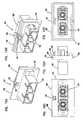
- FIGS. 1A and 1Bshow an example of a jack assembly 20 constructed in accordance with the principles of the present invention.
- the jack assembly 20includes a faceplate 22 adapted to be fastened to a structure such as wall.
- the faceplate 22includes openings 23 for allowing the faceplate 23 to be bolted, screwed or otherwise connected to the wall.
- FIG. 1Ashows a front side of the faceplate 22 adapted to face away from the wall
- FIG. 1Bshows a back side of the faceplate 22 adapted to face toward the wall.
- the faceplate 22defines two rectangular openings 24 positioned one above the other. Each of the openings 24 has a height h o and a width w o .
- two modular jacksare shown mounted in each of the openings 24 of the faceplate 22 .
- two straight jacks 26are shown mounted in the lower opening 24
- two angled jacks 26 ′are shown mounted in the upper opening 24 .
- the jacks 26 , 26 ′include front faces 28 , 28 ′ that define ports 30 , 30 ′ each sized for receiving a plug 32 (shown in FIG. 2 ).
- a plurality of contact springsare positioned within each of the ports 30 , 30 ′.
- the plugs 32include resilient latches 33 .
- the latches 33interlock with front tabs 35 , 35 ′ of the jacks 26 , 26 ′ to retain the plugs 32 within the ports 30 , 30 ′.
- the latches 33are depressed thereby allowing the plugs 32 to be pulled from the ports 30 , 30 ′.
- the jacks 26 , 26 ′ and the plugs 32are eight contact type (i.e., four twisted pair) connectors. While the various aspects of the present invention are particularly useful for modular connectors, it will be appreciated that other types of connectors could also be used.
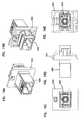
- the straight jack 26includes two basic components: a front jack housing 36 ; and a rear insert assembly 38 .
- the jack housing 36is adapted to be snap-fit into one of the openings 24 of the faceplate 22 .
- the insert assembly 38is adapted to be snap-fit within the jack housing 36 .
- the insert assembly 38is first connected to the jack housing 36 , and then the jack 26 is inserted from the front side of the faceplate 22 into one of the openings 24 .
- the jack housing 36includes a front portion 40 positioned opposite from a back portion 42 .
- the front portion 40 of the jack housing 36includes structure for securing the jack 26 in the faceplate 22 .
- the front portion 40includes a first retaining structure 44 positioned opposite from a second retaining structure 46 .
- Each of the retaining structures 44 , 46includes spaced-apart retaining lips/shoulders 48 separated by a gap 50 .
- Each of the retaining shoulders 48preferably has a width w s
- each of the gapspreferably has a width w g . It is preferred for each of the widths w g to be equal to or less than each of the widths w s .
- the widths w s and w gcooperate to define a total width w s of the jack housing 36 .
- the jack housing 36also preferably includes a height h j defined between the first and second retaining structures 44 and 46 . It is preferred for the height h j to be larger than the height h o of the openings 24 defined by the faceplate 22 .
- the first retaining structure 44includes a first resilient cantilever member 52 positioned between the retaining shoulders 48 of the first retaining structure 44 .
- the second retaining structure 46includes a resilient cantilever member 54 positioned between the retaining shoulders 48 of the second retaining structure 46 .
- Each of the cantilever members 52 , 54includes a base end integrally formed with the jack housing 36 , and a free end positioned adjacent to the front face 28 of the jack 26 .
- the free ends of the cantilever members 52 , 54are flush or slightly recessed with respect to the front face 28 .
- Each of the cantilever members 52 and 54also preferably has a width w c measured at the base ends of the cantilever members 52 , 54 .
- the total width W t of the jack 26is at least two times as large as the width w c . Such a size relationship assists in insuring that the cantilever members 52 , 54 can be easily flexed.
- the resilient cantilever member 54includes a rear tab 56 adapted for engaging the back side of the faceplate 22 .
- the resilient cantilever member 52also includes a rear tab 58 for engaging the back side of the faceplate 22 .
- the cantilever member 52further includes a front tab 60 for engaging the front side of the faceplate 22 .
- the cantilever member 52at least partially defines a portion of the port 30 of the jack 26 . As a result, no portion of the jack housing 36 is provided for preventing the cantilever member 52 from being overflexed.
- the cantilever member 52includes a pair of wings 62 (shown in FIG.
- the wings 62are positioned above recessed deflection limiting surfaces 64 formed on the jack housing 36 . When the cantilever member 52 has been flexed downward a predetermined amount, the wings 62 engage the deflection limiting surfaces 64 to prevent the cantilever member 52 from being overflexed.
- FIG. 8shows the jack 26 snap-fitted within the lower opening 24 of the faceplate 22 .
- the upper and lower sets of retaining shoulders 48engage the front side of the faceplate 22 to prevent the jack housing 36 from being pushed completely through the opening 24 .
- the front tab 60 of the cantilever member 52also engages the front side of the faceplate 22 .
- the rear tabs 56 , 58 of the cantilever members 52 , 54engage the back side of the faceplate 22 to prevent the jack 26 from dislodging from the opening 24 .
- the rear portion of the jackis inserted into the opening 24 .
- the front portion 40 of the jack housing 36defines a inner chamber 66 for housing the contact springs 34 .
- the inner chamber 66can be accessed through the front of the jack housing 36 via the port 30 , and also defines a rear opening 68 for allowing at least a portion of the insert assembly 38 to be inserted into the inner chamber 66 .
- a comb 70is secured to the jack housing 36 within the inner chamber 66 .
- the comb 70includes a plurality of dividers defining a plurality of slots. The slots are sized for receiving portions of the contact springs 34 such that the contact springs 34 are separated from one another.
- Guide rails 72are positioned on opposite sides of the comb 70 .
- the guide rails 72project into the inner chamber 66 from sidewalls of the jack housing 36 .
- the guide rails 72each have a tapered vertical thickness such that the guide rails 72 are thicker adjacent the front side of the inner chamber 66 as compared to the rear side of the inner chamber 66 .
- Latch openings 74are defined by the sidewalls of the jack housing 36 at locations above the guide rails 72 .
- the back portion 42 of the jack housing 36defines an open channel or trough 76 that extends in a rearward direction from the front portion 40 .
- the trough 76is preferably sized to receive and support the insert assembly 38 when the insert assembly is connected to the jack housing 36 .
- the insert assembly 38includes a printed circuit board 78 , a connector mount 80 , the contact springs 34 , a plurality of insulation displacement terminals 82 , and a termination cap 84 .
- the contact springs 34 and the insulation displacement terminals 82respectively include board contact portions 86 , 88 that extend through the connector mount 80 and engage respective contact locations 90 , 92 (e.g., plated through-holes) located on the printed circuit board 78 .
- the printed circuit board 78includes a plurality of tracings 79 (only a representative one is shown) that electrically connect the contact locations 90 to the contact locations 92 . In this manner, the printed circuit board 78 provides electrical connections between the contact springs 34 and the insulation displacement terminals 82 .
- the connector mount 80preferably comprises a one-piece, plastic member having a main body 96 including a first side 98 positioned opposite from a second side 100 .
- the printed circuit board 78is mounted at the second side 100 of the main body 96 .
- the first side 98 of the main body 96is configured for holding or retaining the contact springs 34 and the insulation displacement terminals 82 .
- the first side 98 of the main body 96includes two combs 102 , 104 (shown in FIG. 6 ) for receiving and separating the contact springs 34 .
- Each of the combs 102 , 104includes a plurality of dividers 103 defining slots sized for receiving the contact springs 34 .
- the first side 98 of the main body 96also includes an insulation displacement terminal housing 106 .
- the insulation displacement terminal housing 106defines a plurality of slots 108 in which the insulation displacement terminals 82 are mounted.
- the slots 108are sized to receive wires (not shown) desired to be terminated at the insert assembly 38 .
- the termination cap 84is configured for pressing the wires (not shown) into the slots 108 such that the wires are connected to the insulation displacement terminals 82 .
- the termination cap 84includes a plurality of slotted walls 110 that fit within the slots 108 when the termination cap 84 is pressed down against the insulation displacement terminal housing 106 .
- the connector mount 80also includes two resilient locking tabs 112 integrally connected to the main body 96 for securing the insert assembly 38 to the jack housing 36 .
- the resilient locking tabs 112include flexible lever members 114 positioned on opposite sides of the combs 102 , 104 .
- the locking tabs 112are configured to snap within the latch openings 74 defined by the jack housing 36 to provide a snap-fit connection between the insert assembly 38 and the jack housing 36 .
- the lever members 114are shown connected to the main body 96 of the connector mount 80 , it will be appreciated that alternative snap-fit connecting structures could also be used.
- the connector mount 80could include holes, projections, or latches adapted to interlock with resilient tabs connected to the jack housing 36 .
- the main body 96 of the connector mount 80defines two slots 116 sized and positioned for receiving the guide rails 72 of the jack housing 36 .
- the slots 116are formed within sidewalls of the main body 96 and are positioned on opposite sides of the combs 102 , 104 . Inner ends of the slots 116 are ramped to further enhance alignment between the jack housing 36 and the insert assembly 38 .
- the contact springs 34each preferably includes a base portion 118 and a free end portion 120 .
- the base portions 118fit within the slots defined by the comb 102
- the free end portions 120are aligned above the slots defined by the comb 104 .
- adjacent springs 34have non-parallel relationships with respect to one another to minimize crosstalk.
- the assembled insert assembly 38(shown in FIG. 7A ) is placed within the trough 76 of the jack housing 36 .
- the insert assemblyis positioned such that the circuit board 78 is received in the trough 76 , and the main body 96 of the connector mount 80 is supported by side walls 77 of the trough 76 (e.g., shoulders 79 of the main body 96 seat upon the tops of the side walls 77 ).
- the printed circuit board 78is vertically offset from the bed of the trough 76 .
- the insert assembly 38is moved along the trough 76 in a forward direction such that a front end of the insert assembly 38 (e.g. the end at which the contact springs 34 are mounted) moves into the inner chamber 66 of the jack housing 36 through the rear opening 68 of the jack housing 36 .
- a front end of the insert assembly 38e.g. the end at which the contact springs 34 are mounted
- the guide rails 72 of the jack housing 36are received within the guide slots 116 defined by the connector mount 80 .
- the free end portions 120 of the contact springs 34are received within the slots defined by the comb 70 located within the inner chamber 66 .
- the locking tabs 112 of the connector mount 80snap within the latch openings 74 of the jack housing 36 .
- the locking tabs 112can be depressed thereby allowing the insert assembly 38 to be pulled from the jack housing 36 .
- the guide rails 72 and the guide slots 116provide for precise positioning of the connector mount 80 within the jack housing 36 .
- the guide slots 166 and the guide rails 72are configured to orient the connector mount 80 at a precise vertical and horizontal position relative to the comb 70 .
- the springs 34are received within the comb 70
- the printed circuit board 78is preferably offset from or held above the bed of the trough 76 . Because the board 78 is offset from the trough 76 , printed circuit boards having different thicknesses can be used without affecting the alignment of the connector mount 80 within the jack housing 36 .
- the alignment of the connector mount 80 within the jack housing 36is not dependent upon the thickness of the circuit board 78 . Therefore, the rail and slot configuration eliminates variations in spring deflection and the resulting contact forces caused by tolerance variations in the thickness of the printed circuit boards.
- FIG. 9is a cross-sectional view taken along section line 9 — 9 of FIG. 8 .
- the comb 70 secured with in the jack housing 36 and the comb 104 connected to the connector mount 80oppose one another and are aligned generally along a common vertical plane.
- the combs 70 and 104cooperate to form closed ended slots 122 in which the free end portions 120 of the contact springs 34 are received.
- Vertical spacing s between the combs 70 and 104is preferably sufficiently small to prevent the free end portions 120 of the springs 34 from becoming displaced from the slots 122 . In this manner, the free end portions 120 of the springs 34 are captured between the two separate combs 70 and 104 .
- the spring alignment feature provided by the combs 70 and 104is important because the contact springs 34 typically have a center to center spacing of about 0.050 inches. When a plug is inserted into the port 30 , the plug engages the springs 34 causing the springs to deflect downwardly out of the comb 70 . Absent the two cooperating combs 70 and 104 , the springs can become misaligned and pushed into contact with one other during deflection. This is not surprising due to the relatively close spacing of the springs 34 . However, by capturing the springs 34 between the two combs 70 and 104 as described above, such misalignment is prevented because the springs 34 always remain within their respective closed ended slots 122 during deflection.
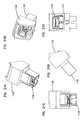
- FIGS. 10 and 11illustrate one of the angled jacks 26 ′.
- the angled jack 26 ′uses the same insert assembly 38 used by the straight jack 26 . Consequently, no further description of the insert assembly 38 will be provided.
- the angled jack 26 ′includes a jack housing 36 ′ that is similar to the jack housing 36 described with respect to the straight jack 26 . However, the jack housing 36 ′ has been modified to allow the jack 26 ′ to mount at an angle relative to the faceplate 22 .
- the jack housing 36 ′includes first and second retaining structures 44 ′ and 46 ′ for providing a snap-fit connection between the jack 26 ′ and the faceplate 22 .
- the first and second retaining structures 44 ′, 46 ′are preferably aligned along a line 124 that is oriented at an acute angle ⁇ relative to the front face 28 ′ of the jack 26 ′. Consequently, when the jack 26 ′ is secured to the faceplate 22 , the retaining structures 44 ′, 46 ′ cause the front face 28 ′ of the jack 26 ′ to be angled relative to the front face of the faceplate 22 .
- the first retaining structure 44includes two fixed retaining shoulders 126 (only one shown) positioned at opposite sides of the jack housing 36 ′.
- the second retaining structure 46 ′includes two spaced-apart retaining shoulders 128 positioned on opposite sides of the jack housing 36 ′.
- a gap 130separates the retaining shoulders 128 .
- a resilient cantilever member 132is positioned within the gap 130 .
- the cantilever member 132includes a rear stop 134 adapted to engage the back side of the faceplate 22 .
- the retaining shoulders 126 , 128engage the front side of the faceplate 22
- the rear stop 134 of the cantilever member 132engages the back side of the faceplate 22 .
- the rear portion of the jackis inserted into the opening 24 and the jack 26 ′ is pushed into the opening 24 .
- a ramped surface of the rear stop 134causes the cantilever member 132 to flex upward until the rear stop 134 passes through the opening 24 .
- the cantilever member 132snaps downward thereby bringing the rear stop 134 into engagement with the back side of the faceplate 22 .
- the entire jack 26 ′can be removed from the faceplate 22 by flexing the cantilever member 132 upward, and concurrently pulling the jack 26 ′ from the opening 24 .
- FIGS. 12A-12E13 A- 13 E, 14 A- 14 E, 15 A- 15 E, 16 A- 16 E, 17 A- 17 E, 18 A- 18 E, 19 A- 19 E, 20 A- 20 E, and 21 A- 21 E illustrate a variety of different telecommunications connectors that can be mounted in the openings 24 of the faceplate 22 .
- FIGS. 12A-12Eillustrate a straight ST type connector 220 mounted on a support structure or adapter 222 configured to be snap-fit within one of the openings 24 of the faceplate 22 .
- the adapter 22 222includes top and bottom shoulders 224 and 226 adapted to engage the front side of the faceplate, and a resilient cantilever member 228 having a rear stop 230 adapted to engage the back side of the faceplate.
- the adapter 22 222has a total width generally equal to one-half the width of the opening 24 of the faceplate 22 .
- the member 228preferably has a base end having a width less than or equal to one-half the total width 222 of the adapter.
- the cantilever 228is preferably positioned within a gap 232 having a width that is less than or equal to corresponding widths of the shoulders 224 .
- FIGS. 13A-13Eshow a straight RCA-type connector 320 secured to an adapter 322 configured to snap-fit within the faceplate 22 .
- FIGS. 14A-14Eillustrate a straight F-type connector 420 mounted on an adapter 422 configured to snap-fit within the faceplate 22 .
- FIGS. 16-16Eshow a straight SC-type connector 620 mounted on an adapter 622 configured to snap-fit within the faceplate 22 .
- FIGS. 18A-18Eillustrate a straight BNC-type connector 820 mounted on an adapter 822 configured to snap-fit within the faceplate 22 .
- Each of the adapters 332 , 422 , 622 and 822has a similar size and configuration as the adapter 222 of FIGS. 12A-12E .
- FIGS. 15A-15Eillustrates a straight duplex SC-type connector 520 mounted on an adapter 522 configured to snap within one of the openings 24 of the faceplate 22 .
- the adapter 522is sized to entirely fill one of the holes 24 defined by the faceplate 22 .
- the adapter 522includes a lower retaining structure 526 (e.g., a slot) and an upper retaining structure 524 .
- the upper retaining structure 524includes two front shoulders 528 and a resilient cantilever 530 positioned between the shoulders 528 .
- the cantilever 530includes a rear stop 532 .
- FIGS. 17A-17Eillustrate an angled duplex SC-type connector 720 mounted on an adapter 722 .
- the adapteris sized to fill an entire one of the holes 24 of the faceplate 22 .
- the adapter 722includes first and second oppositely positioned retaining structures 724 , 726 adapted to provide a snap-fit connection with the faceplate 22 .
- the retaining structures 724 , 726are aligned along a line that is oriented at an acute angle with respect to a front face 728 of the connector 720 .
- FIGS. 19A-19Eillustrates a blank 922 configured for covering one half of one of the openings 24 of the faceplate 22 .
- the blank 922has a planar cover surface 924 .
- the blank 922also includes first and second oppositely positioned retaining structures 924 and 926 for providing a snap-fit connection with the faceplate 22 .
- FIGS. 20A-20Eillustrate an angled ST-type connector 1020 mounted on an adapter 1022 .
- the adapter 1022is sized to fill one-half of one of the openings 24 of the faceplate 22 .
- the adapter 1022includes first and second retaining structures 1024 and 1026 configured to provide a snap-fit connection with the faceplate.
- the retaining structures 1024 , 1026are aligned along a line or at an acute angle with respect to the front face of the connector 1020 .
- FIGS. 21A-21Eillustrate an angled SC-type connector 1120 mounted on an adapter 1122 .
- the adapter 1122has substantially the same size and configuration as the adapter 1022 of FIGS. 20A-20E .
Landscapes
- Coupling Device And Connection With Printed Circuit (AREA)
- Details Of Connecting Devices For Male And Female Coupling (AREA)
Abstract
Description
Claims (46)
Priority Applications (1)
| Application Number | Priority Date | Filing Date | Title |
|---|---|---|---|
| US11/067,619USRE40682E1 (en) | 1999-01-15 | 2005-02-25 | Telecommunications jack assembly |
Applications Claiming Priority (4)
| Application Number | Priority Date | Filing Date | Title |
|---|---|---|---|
| US09/231,736US6334792B1 (en) | 1999-01-15 | 1999-01-15 | Connector including reduced crosstalk spring insert |
| US09/327,053US6234836B1 (en) | 1999-01-15 | 1999-06-07 | Telecommunications jack assembly |
| US09/828,575US6524131B2 (en) | 1999-01-15 | 2001-04-04 | Telecommunications jack assembly |
| US11/067,619USRE40682E1 (en) | 1999-01-15 | 2005-02-25 | Telecommunications jack assembly |
Related Parent Applications (1)
| Application Number | Title | Priority Date | Filing Date |
|---|---|---|---|
| US09/828,575ReissueUS6524131B2 (en) | 1999-01-15 | 2001-04-04 | Telecommunications jack assembly |
Publications (1)
| Publication Number | Publication Date |
|---|---|
| USRE40682E1true USRE40682E1 (en) | 2009-03-24 |
Family
ID=22870466
Family Applications (5)
| Application Number | Title | Priority Date | Filing Date |
|---|---|---|---|
| US09/231,736Expired - LifetimeUS6334792B1 (en) | 1999-01-15 | 1999-01-15 | Connector including reduced crosstalk spring insert |
| US09/327,053Expired - LifetimeUS6234836B1 (en) | 1999-01-15 | 1999-06-07 | Telecommunications jack assembly |
| US10/023,051CeasedUS6629862B2 (en) | 1999-01-15 | 2001-12-17 | Connector including reduced crosstalk spring insert |
| US11/067,617Expired - LifetimeUSRE40575E1 (en) | 1999-01-15 | 2005-02-25 | Connector including reduced crosstalk spring insert |
| US11/067,619Expired - LifetimeUSRE40682E1 (en) | 1999-01-15 | 2005-02-25 | Telecommunications jack assembly |
Family Applications Before (4)
| Application Number | Title | Priority Date | Filing Date |
|---|---|---|---|
| US09/231,736Expired - LifetimeUS6334792B1 (en) | 1999-01-15 | 1999-01-15 | Connector including reduced crosstalk spring insert |
| US09/327,053Expired - LifetimeUS6234836B1 (en) | 1999-01-15 | 1999-06-07 | Telecommunications jack assembly |
| US10/023,051CeasedUS6629862B2 (en) | 1999-01-15 | 2001-12-17 | Connector including reduced crosstalk spring insert |
| US11/067,617Expired - LifetimeUSRE40575E1 (en) | 1999-01-15 | 2005-02-25 | Connector including reduced crosstalk spring insert |
Country Status (6)
| Country | Link |
|---|---|
| US (5) | US6334792B1 (en) |
| KR (1) | KR20010101856A (en) |
| CN (1) | CN1897365A (en) |
| AR (1) | AR022287A1 (en) |
| RU (1) | RU2001121483A (en) |
| ZA (1) | ZA200106240B (en) |
Cited By (1)
| Publication number | Priority date | Publication date | Assignee | Title |
|---|---|---|---|---|
| US20120069516A1 (en)* | 2010-09-22 | 2012-03-22 | Panasonic Corporation | Electronic apparatus |
Families Citing this family (48)
| Publication number | Priority date | Publication date | Assignee | Title |
|---|---|---|---|---|
| JP2002535809A (en) | 1999-01-15 | 2002-10-22 | エーデーシー・テレコミュニケーションズ・インコーポレーテッド | Communication Jack Assembly |
| US6334792B1 (en)* | 1999-01-15 | 2002-01-01 | Adc Telecommunications, Inc. | Connector including reduced crosstalk spring insert |
| US6543626B1 (en)* | 1999-05-21 | 2003-04-08 | Adc Telecommunications, Inc. | Cable management rack for telecommunication cross-connect systems |
| US6508593B1 (en)* | 2000-05-09 | 2003-01-21 | Molex Incorporated | Universal panel mount system for fiber optic connecting devices |
| US6749466B1 (en)* | 2000-08-14 | 2004-06-15 | Hubbell Incorporated | Electrical connector contact configurations |
| US6616005B1 (en)* | 2000-08-28 | 2003-09-09 | Hubbell Incorporated | Modular faceplate assembly for an electrical box |
| US6554653B2 (en)* | 2001-03-16 | 2003-04-29 | Adc Telecommunications, Inc. | Telecommunications connector with spring assembly and method for assembling |
| US6736670B2 (en)* | 2001-11-16 | 2004-05-18 | Adc Telecommunications, Inc. | Angled RJ to RJ patch panel |
| JP4061123B2 (en)* | 2002-05-21 | 2008-03-12 | 日立電線株式会社 | Modular jack connector |
| US6814624B2 (en)* | 2002-11-22 | 2004-11-09 | Adc Telecommunications, Inc. | Telecommunications jack assembly |
| US7052328B2 (en)* | 2002-11-27 | 2006-05-30 | Panduit Corp. | Electronic connector and method of performing electronic connection |
| EP1881570B1 (en)* | 2002-11-27 | 2009-07-29 | Panduit Corporation | Electronic connector and method of performing electronic connection |
| US6830488B2 (en)* | 2003-05-12 | 2004-12-14 | Krone, Inc. | Modular jack with wire management |
| US7704404B2 (en)* | 2003-07-17 | 2010-04-27 | Honeywell International Inc. | Refrigerant compositions and use thereof in low temperature refrigeration systems |
| USD511325S1 (en)* | 2003-09-15 | 2005-11-08 | Leviton Manufacturing Co., Inc. | Back end portion of an electrical connector jack |
| US7232340B2 (en)* | 2004-02-20 | 2007-06-19 | Adc Incorporated | Methods and systems for minimizing alien crosstalk between connectors |
| CA2464834A1 (en) | 2004-04-19 | 2005-10-19 | Nordx/Cdt Inc. | Connector |
| DE102004042586B3 (en)* | 2004-09-02 | 2005-12-08 | Adc Gmbh | Electrical connection module |
| US7040933B1 (en)* | 2005-05-02 | 2006-05-09 | Hsing Chau Industrial Co., Ltd | Modular communication jack with low assembling tolerance |
| US8350154B1 (en)* | 2005-08-23 | 2013-01-08 | Hubbell Incorporated | Universal wall plate mount |
| US7294024B2 (en)* | 2006-01-06 | 2007-11-13 | Adc Telecommunications, Inc. | Methods and systems for minimizing alien crosstalk between connectors |
| US7651380B2 (en)* | 2006-02-08 | 2010-01-26 | The Siemon Company | Modular plugs and outlets having enhanced performance contacts |
| US7232337B1 (en)* | 2006-03-13 | 2007-06-19 | Tyco Electronics Corporation | Connector receptacle assembly |
| DK2044654T3 (en)* | 2006-07-25 | 2010-04-19 | Adc Gmbh | connection block |
| CN101455091B (en)* | 2006-07-25 | 2013-03-13 | Adc有限公司 | Connector block |
| AU313574S (en) | 2006-07-25 | 2007-04-10 | Tyco Electronics Services Gmbh | Connector block |
| CN201608967U (en)* | 2006-11-14 | 2010-10-13 | 莫列斯公司 | Crosstalk compensation component, printed circuit board, module jack and socket terminals |
| CN103107438B (en)* | 2006-12-01 | 2016-05-04 | 西蒙公司 | The telecommunications plug coordinating with tele-communication jacks |
| AU2007201113B2 (en) | 2007-03-14 | 2011-09-08 | Tyco Electronics Services Gmbh | Electrical Connector |
| AU2007201114B2 (en)* | 2007-03-14 | 2011-04-07 | Tyco Electronics Services Gmbh | Electrical Connector |
| AU2007201109B2 (en)* | 2007-03-14 | 2010-11-04 | Tyco Electronics Services Gmbh | Electrical Connector |
| AU2007201107B2 (en) | 2007-03-14 | 2011-06-23 | Tyco Electronics Services Gmbh | Electrical Connector |
| AU2007201106B9 (en)* | 2007-03-14 | 2011-06-02 | Tyco Electronics Services Gmbh | Electrical Connector |
| AU2007201108B2 (en)* | 2007-03-14 | 2012-02-09 | Tyco Electronics Services Gmbh | Electrical Connector |
| AU2007201105B2 (en) | 2007-03-14 | 2011-08-04 | Tyco Electronics Services Gmbh | Electrical Connector |
| AU2007201102B2 (en)* | 2007-03-14 | 2010-11-04 | Tyco Electronics Services Gmbh | Electrical Connector |
| US7794286B2 (en)* | 2008-12-12 | 2010-09-14 | Hubbell Incorporated | Electrical connector with separate contact mounting and compensation boards |
| TWM414715U (en)* | 2011-01-28 | 2011-10-21 | Paul Foung | Front load keystone d-shape connector |
| WO2013112858A1 (en)* | 2012-01-27 | 2013-08-01 | Go!Foton Holdings, Inc. | Patch panel assembly |
| US8512082B1 (en)* | 2012-02-10 | 2013-08-20 | Yfc-Boneagle Electric Co., Ltd. | Electrical connector jack |
| CN102740637B (en)* | 2012-06-07 | 2016-01-20 | 惠州德赛信息科技有限公司 | Electronic unit with external interface on electronic product and this electronic product |
| CN203242790U (en)* | 2013-03-19 | 2013-10-16 | 泰科电子(上海)有限公司 | Connector |
| CN105406232B (en)* | 2014-08-20 | 2018-02-02 | 富士康(昆山)电脑接插件有限公司 | RJ45 socket connectors |
| US10291969B2 (en) | 2017-02-14 | 2019-05-14 | Go!Foton Holdings, Inc. | Rear cable management |
| BE1025936B1 (en)* | 2018-01-22 | 2019-08-21 | Phoenix Contact Gmbh & Co Kg | Modular system for manufacturing an electrical device |
| EP3971622A1 (en) | 2020-07-02 | 2022-03-23 | Go!Foton Holdings, Inc. | Intelligent optical switch |
| EP4063929A1 (en)* | 2021-01-18 | 2022-09-28 | Sterlite Technologies Limited | Enclosure with converging ports |
| US12401163B2 (en)* | 2021-10-28 | 2025-08-26 | Panduit Corp. | Single pair connector module |
Citations (68)
| Publication number | Priority date | Publication date | Assignee | Title |
|---|---|---|---|---|
| US4274691A (en) | 1978-12-05 | 1981-06-23 | Amp Incorporated | Modular jack |
| US4406509A (en) | 1981-11-25 | 1983-09-27 | E. I. Du Pont De Nemours & Co. | Jack and plug electrical assembly |
| US4556264A (en) | 1983-03-15 | 1985-12-03 | Hosiden Electronics Co., Ltd. | Telephone connector |
| US4648678A (en) | 1985-07-01 | 1987-03-10 | Brand-Rex Company | Electrical connector |
| US4698025A (en) | 1986-09-15 | 1987-10-06 | Molex Incorporated | Low profile modular phone jack assembly |
| US4971571A (en) | 1990-03-15 | 1990-11-20 | Amp Incorporated | Self-locking pin field connector |
| US5030123A (en) | 1989-03-24 | 1991-07-09 | Adc Telecommunications, Inc. | Connector and patch panel for digital video and data |
| US5041018A (en) | 1990-08-20 | 1991-08-20 | At&T Bell Laboratories | Electrical connector receptacle |
| US5044981A (en) | 1990-04-18 | 1991-09-03 | Reliance Comm/Tec Corporation | Snap-on stacking telephone jack |
| US5071371A (en) | 1990-03-30 | 1991-12-10 | Molex Incorporated | Electrical card edge connector assembly |
| US5156554A (en) | 1989-10-10 | 1992-10-20 | Itt Corporation | Connector interceptor plate arrangement |
| US5186647A (en) | 1992-02-24 | 1993-02-16 | At&T Bell Laboratories | High frequency electrical connector |
| US5238426A (en) | 1992-06-11 | 1993-08-24 | At&T Bell Laboratories | Universal patch panel for communications use in buildings |
| US5299956A (en) | 1992-03-23 | 1994-04-05 | Superior Modular Products, Inc. | Low cross talk electrical connector system |
| US5302140A (en) | 1993-04-02 | 1994-04-12 | At&T Bell Laboratories | Connector with mounting collar for use in universal patch panel systems |
| US5338231A (en) | 1992-05-08 | 1994-08-16 | Molex Incorporated | Electrical connector with contact anti-overstress means |
| US5362257A (en) | 1993-07-08 | 1994-11-08 | The Whitaker Corporation | Communications connector terminal arrays having noise cancelling capabilities |
| US5399107A (en) | 1992-08-20 | 1995-03-21 | Hubbell Incorporated | Modular jack with enhanced crosstalk performance |
| US5403200A (en) | 1994-05-04 | 1995-04-04 | Chen; Michael | Electric connecting block |
| US5474474A (en) | 1992-12-18 | 1995-12-12 | The Siemon Company | Electrically balanced connector assembly |
| US5478261A (en) | 1978-06-14 | 1995-12-26 | Virginia Patent Development Corp. | Modular jack for directly coupling modular plug with printed circuit board |
| US5503572A (en) | 1994-05-17 | 1996-04-02 | Mod-Tap Corporation | Communications connectors |
| US5580257A (en) | 1995-04-28 | 1996-12-03 | Molex Incorporated | High performance card edge connector |
| US5624274A (en) | 1995-11-07 | 1997-04-29 | International Connectors And Cable Corporation | Telephone connector with contact protection block |
| EP0777304A2 (en) | 1995-11-28 | 1997-06-04 | Molex Incorporated | Electrical connector |
| US5639261A (en) | 1994-12-23 | 1997-06-17 | Lucent Technologies Inc. | Modular cross-connect system |
| US5639266A (en) | 1994-01-11 | 1997-06-17 | Stewart Connector Systems, Inc. | High frequency electrical connector |
| US5647043A (en) | 1995-10-12 | 1997-07-08 | Lucent Technologies, Inc. | Unipartite jack receptacle |
| US5659650A (en) | 1995-09-26 | 1997-08-19 | Lucent Technologies Inc. | Hinged faceplate |
| US5674093A (en) | 1996-07-23 | 1997-10-07 | Superior Modular Process Incorporated | Reduced cross talk electrical connector |
| WO1997044862A1 (en) | 1996-05-23 | 1997-11-27 | The Siemon Company | Reduced crosstalk modular outlet |
| US5700167A (en) | 1996-09-06 | 1997-12-23 | Lucent Technologies | Connector cross-talk compensation |
| GB2314466A (en) | 1996-06-21 | 1997-12-24 | Lucent Technologies Inc | Capacitor array for reducing cross-talk in connectors |
| US5713764A (en) | 1992-03-16 | 1998-02-03 | Molex Incorporated | Impedance and inductance control in electrical connectors |
| US5716237A (en) | 1996-06-21 | 1998-02-10 | Lucent Technologies Inc. | Electrical connector with crosstalk compensation |
| US5735714A (en) | 1995-04-06 | 1998-04-07 | Ortronics Inc. | Information management outlet module and assembly providing protection to exposed cabling |
| US5759070A (en) | 1994-11-30 | 1998-06-02 | Berg Technology, Inc. | Modular jack insert |
| US5779503A (en) | 1996-12-18 | 1998-07-14 | Nordx/Cdt, Inc. | High frequency connector with noise cancelling characteristics |
| US5785546A (en) | 1995-11-27 | 1998-07-28 | Yazaki Corporation | Connector locking structure |
| US5791943A (en) | 1995-11-22 | 1998-08-11 | The Siemon Company | Reduced crosstalk modular outlet |
| US5791935A (en) | 1995-06-30 | 1998-08-11 | Yazaki Corporation | Connector with a fitting-completion detector |
| US5795186A (en) | 1996-09-18 | 1998-08-18 | The Siemon Company | Multimedia bezels |
| US5885111A (en) | 1998-01-13 | 1999-03-23 | Shiunn Yang Enterprise Co., Ltd. | Keystone jack for digital communication networks |
| US5911602A (en) | 1996-07-23 | 1999-06-15 | Superior Modular Products Incorporated | Reduced cross talk electrical connector |
| US5924896A (en) | 1997-08-01 | 1999-07-20 | Lucent Technologies Inc. | High frequency communication jack |
| US5938479A (en) | 1997-04-02 | 1999-08-17 | Communications Systems, Inc. | Connector for reducing electromagnetic field coupling |
| US5941734A (en) | 1995-12-25 | 1999-08-24 | Matsushita Electric Works, Ltd. | Connector |
| US5947761A (en) | 1998-09-29 | 1999-09-07 | The Whitaker Corporation | Electrical connector with pivoting wire fixture |
| US5947772A (en) | 1997-08-22 | 1999-09-07 | Lucent Technologies Inc. | Wire terminal block for communication connectors |
| US5997358A (en) | 1997-09-02 | 1999-12-07 | Lucent Technologies Inc. | Electrical connector having time-delayed signal compensation |
| US6066005A (en) | 1998-06-30 | 2000-05-23 | Berg Technology, Inc. | Vertical modular connector having low electrical crosstalk |
| US6083052A (en) | 1998-03-23 | 2000-07-04 | The Siemon Company | Enhanced performance connector |
| US6086428A (en) | 1998-03-25 | 2000-07-11 | Lucent Technologies Inc. | Crosstalk compensation for connector jack |
| US6089909A (en) | 1997-06-02 | 2000-07-18 | Sumitomo Wiring Systems, Ltd. | Connector |
| US6089923A (en) | 1999-08-20 | 2000-07-18 | Adc Telecommunications, Inc. | Jack including crosstalk compensation for printed circuit board |
| WO2000042682A1 (en) | 1999-01-15 | 2000-07-20 | Adc Telecommunications, Inc. | Telecommunications jack assembly |
| US6102722A (en) | 1998-12-28 | 2000-08-15 | Lucent Technologies Inc. | Upgradeable communication connector |
| US6116964A (en) | 1999-03-08 | 2000-09-12 | Lucent Technologies Inc. | High frequency communications connector assembly with crosstalk compensation |
| US6165023A (en) | 1999-10-28 | 2000-12-26 | Lucent Technologies Inc. | Capacitive crosstalk compensation arrangement for a communication connector |
| US6186834B1 (en) | 1999-06-08 | 2001-02-13 | Avaya Technology Corp. | Enhanced communication connector assembly with crosstalk compensation |
| US6196880B1 (en) | 1999-09-21 | 2001-03-06 | Avaya Technology Corp. | Communication connector assembly with crosstalk compensation |
| US6234836B1 (en) | 1999-01-15 | 2001-05-22 | Adc Telecommunications, Inc. | Telecommunications jack assembly |
| US6270358B1 (en) | 1999-04-01 | 2001-08-07 | Infra+ | Low-voltage male connector |
| US6283796B1 (en) | 2000-03-23 | 2001-09-04 | Hon Hai Precision Ind. Co., Ltd. | RJ-receptacle connector with anti-incorrect-insertion device |
| US6350158B1 (en) | 2000-09-19 | 2002-02-26 | Avaya Technology Corp. | Low crosstalk communication connector |
| EP0692884B1 (en) | 1994-07-14 | 2002-03-20 | Molex Incorporated | Modular connector with reduced crosstalk |
| US6371793B1 (en) | 1998-08-24 | 2002-04-16 | Panduit Corp. | Low crosstalk modular communication connector |
| US6814624B2 (en) | 2002-11-22 | 2004-11-09 | Adc Telecommunications, Inc. | Telecommunications jack assembly |
- 1999
- 1999-01-15USUS09/231,736patent/US6334792B1/ennot_activeExpired - Lifetime
- 1999-06-07USUS09/327,053patent/US6234836B1/ennot_activeExpired - Lifetime
- 2000
- 2000-01-04CNCNA200610100352XApatent/CN1897365A/enactivePending
- 2000-01-04RURU2001121483/09Apatent/RU2001121483A/ennot_activeApplication Discontinuation
- 2000-01-04KRKR1020017008947Apatent/KR20010101856A/ennot_activeWithdrawn
- 2000-01-14ARARP000100166Apatent/AR022287A1/enunknown
- 2001
- 2001-07-30ZAZA200106240Apatent/ZA200106240B/enunknown
- 2001-12-17USUS10/023,051patent/US6629862B2/ennot_activeCeased
- 2005
- 2005-02-25USUS11/067,617patent/USRE40575E1/ennot_activeExpired - Lifetime
- 2005-02-25USUS11/067,619patent/USRE40682E1/ennot_activeExpired - Lifetime
Patent Citations (73)
| Publication number | Priority date | Publication date | Assignee | Title |
|---|---|---|---|---|
| US5478261A (en) | 1978-06-14 | 1995-12-26 | Virginia Patent Development Corp. | Modular jack for directly coupling modular plug with printed circuit board |
| US4274691A (en) | 1978-12-05 | 1981-06-23 | Amp Incorporated | Modular jack |
| US4406509A (en) | 1981-11-25 | 1983-09-27 | E. I. Du Pont De Nemours & Co. | Jack and plug electrical assembly |
| US4556264A (en) | 1983-03-15 | 1985-12-03 | Hosiden Electronics Co., Ltd. | Telephone connector |
| US4648678A (en) | 1985-07-01 | 1987-03-10 | Brand-Rex Company | Electrical connector |
| US4698025A (en) | 1986-09-15 | 1987-10-06 | Molex Incorporated | Low profile modular phone jack assembly |
| US5030123A (en) | 1989-03-24 | 1991-07-09 | Adc Telecommunications, Inc. | Connector and patch panel for digital video and data |
| US5156554A (en) | 1989-10-10 | 1992-10-20 | Itt Corporation | Connector interceptor plate arrangement |
| US4971571A (en) | 1990-03-15 | 1990-11-20 | Amp Incorporated | Self-locking pin field connector |
| US5071371A (en) | 1990-03-30 | 1991-12-10 | Molex Incorporated | Electrical card edge connector assembly |
| US5044981A (en) | 1990-04-18 | 1991-09-03 | Reliance Comm/Tec Corporation | Snap-on stacking telephone jack |
| US5041018A (en) | 1990-08-20 | 1991-08-20 | At&T Bell Laboratories | Electrical connector receptacle |
| US5186647A (en) | 1992-02-24 | 1993-02-16 | At&T Bell Laboratories | High frequency electrical connector |
| US5713764A (en) | 1992-03-16 | 1998-02-03 | Molex Incorporated | Impedance and inductance control in electrical connectors |
| US5299956A (en) | 1992-03-23 | 1994-04-05 | Superior Modular Products, Inc. | Low cross talk electrical connector system |
| US5310363A (en) | 1992-03-23 | 1994-05-10 | Superior Modular Products Incorporated | Impedance matched reduced cross talk electrical connector system |
| US5299956B1 (en) | 1992-03-23 | 1995-10-24 | Superior Modular Prod Inc | Low cross talk electrical connector system |
| US5338231A (en) | 1992-05-08 | 1994-08-16 | Molex Incorporated | Electrical connector with contact anti-overstress means |
| US5238426A (en) | 1992-06-11 | 1993-08-24 | At&T Bell Laboratories | Universal patch panel for communications use in buildings |
| US5399107A (en) | 1992-08-20 | 1995-03-21 | Hubbell Incorporated | Modular jack with enhanced crosstalk performance |
| US5474474A (en) | 1992-12-18 | 1995-12-12 | The Siemon Company | Electrically balanced connector assembly |
| US5302140A (en) | 1993-04-02 | 1994-04-12 | At&T Bell Laboratories | Connector with mounting collar for use in universal patch panel systems |
| US5362257A (en) | 1993-07-08 | 1994-11-08 | The Whitaker Corporation | Communications connector terminal arrays having noise cancelling capabilities |
| US5639266A (en) | 1994-01-11 | 1997-06-17 | Stewart Connector Systems, Inc. | High frequency electrical connector |
| US5403200A (en) | 1994-05-04 | 1995-04-04 | Chen; Michael | Electric connecting block |
| US5503572A (en) | 1994-05-17 | 1996-04-02 | Mod-Tap Corporation | Communications connectors |
| EP0692884B1 (en) | 1994-07-14 | 2002-03-20 | Molex Incorporated | Modular connector with reduced crosstalk |
| US5759070A (en) | 1994-11-30 | 1998-06-02 | Berg Technology, Inc. | Modular jack insert |
| US5639261A (en) | 1994-12-23 | 1997-06-17 | Lucent Technologies Inc. | Modular cross-connect system |
| US5735714A (en) | 1995-04-06 | 1998-04-07 | Ortronics Inc. | Information management outlet module and assembly providing protection to exposed cabling |
| US5580257A (en) | 1995-04-28 | 1996-12-03 | Molex Incorporated | High performance card edge connector |
| US5791935A (en) | 1995-06-30 | 1998-08-11 | Yazaki Corporation | Connector with a fitting-completion detector |
| US5659650A (en) | 1995-09-26 | 1997-08-19 | Lucent Technologies Inc. | Hinged faceplate |
| US5647043A (en) | 1995-10-12 | 1997-07-08 | Lucent Technologies, Inc. | Unipartite jack receptacle |
| US5624274A (en) | 1995-11-07 | 1997-04-29 | International Connectors And Cable Corporation | Telephone connector with contact protection block |
| US5791943A (en) | 1995-11-22 | 1998-08-11 | The Siemon Company | Reduced crosstalk modular outlet |
| US5785546A (en) | 1995-11-27 | 1998-07-28 | Yazaki Corporation | Connector locking structure |
| EP0777304A2 (en) | 1995-11-28 | 1997-06-04 | Molex Incorporated | Electrical connector |
| US5941734A (en) | 1995-12-25 | 1999-08-24 | Matsushita Electric Works, Ltd. | Connector |
| WO1997044862A1 (en) | 1996-05-23 | 1997-11-27 | The Siemon Company | Reduced crosstalk modular outlet |
| US5716237A (en) | 1996-06-21 | 1998-02-10 | Lucent Technologies Inc. | Electrical connector with crosstalk compensation |
| GB2314466A (en) | 1996-06-21 | 1997-12-24 | Lucent Technologies Inc | Capacitor array for reducing cross-talk in connectors |
| US5911602A (en) | 1996-07-23 | 1999-06-15 | Superior Modular Products Incorporated | Reduced cross talk electrical connector |
| US5674093A (en) | 1996-07-23 | 1997-10-07 | Superior Modular Process Incorporated | Reduced cross talk electrical connector |
| US5700167A (en) | 1996-09-06 | 1997-12-23 | Lucent Technologies | Connector cross-talk compensation |
| US5795186A (en) | 1996-09-18 | 1998-08-18 | The Siemon Company | Multimedia bezels |
| US5779503A (en) | 1996-12-18 | 1998-07-14 | Nordx/Cdt, Inc. | High frequency connector with noise cancelling characteristics |
| US5938479A (en) | 1997-04-02 | 1999-08-17 | Communications Systems, Inc. | Connector for reducing electromagnetic field coupling |
| US6089909A (en) | 1997-06-02 | 2000-07-18 | Sumitomo Wiring Systems, Ltd. | Connector |
| US5924896A (en) | 1997-08-01 | 1999-07-20 | Lucent Technologies Inc. | High frequency communication jack |
| US5947772A (en) | 1997-08-22 | 1999-09-07 | Lucent Technologies Inc. | Wire terminal block for communication connectors |
| US5997358A (en) | 1997-09-02 | 1999-12-07 | Lucent Technologies Inc. | Electrical connector having time-delayed signal compensation |
| US5885111A (en) | 1998-01-13 | 1999-03-23 | Shiunn Yang Enterprise Co., Ltd. | Keystone jack for digital communication networks |
| US6083052A (en) | 1998-03-23 | 2000-07-04 | The Siemon Company | Enhanced performance connector |
| US6086428A (en) | 1998-03-25 | 2000-07-11 | Lucent Technologies Inc. | Crosstalk compensation for connector jack |
| US6066005A (en) | 1998-06-30 | 2000-05-23 | Berg Technology, Inc. | Vertical modular connector having low electrical crosstalk |
| US6371793B1 (en) | 1998-08-24 | 2002-04-16 | Panduit Corp. | Low crosstalk modular communication connector |
| US5947761A (en) | 1998-09-29 | 1999-09-07 | The Whitaker Corporation | Electrical connector with pivoting wire fixture |
| US6102722A (en) | 1998-12-28 | 2000-08-15 | Lucent Technologies Inc. | Upgradeable communication connector |
| WO2000042682A1 (en) | 1999-01-15 | 2000-07-20 | Adc Telecommunications, Inc. | Telecommunications jack assembly |
| US6524131B2 (en) | 1999-01-15 | 2003-02-25 | Adc Telecommunications, Inc. | Telecommunications jack assembly |
| US6334792B1 (en) | 1999-01-15 | 2002-01-01 | Adc Telecommunications, Inc. | Connector including reduced crosstalk spring insert |
| US6234836B1 (en) | 1999-01-15 | 2001-05-22 | Adc Telecommunications, Inc. | Telecommunications jack assembly |
| US6629862B2 (en) | 1999-01-15 | 2003-10-07 | Adc Telecommunications, Inc. | Connector including reduced crosstalk spring insert |
| US6116964A (en) | 1999-03-08 | 2000-09-12 | Lucent Technologies Inc. | High frequency communications connector assembly with crosstalk compensation |
| US6270358B1 (en) | 1999-04-01 | 2001-08-07 | Infra+ | Low-voltage male connector |
| US6186834B1 (en) | 1999-06-08 | 2001-02-13 | Avaya Technology Corp. | Enhanced communication connector assembly with crosstalk compensation |
| US6089923A (en) | 1999-08-20 | 2000-07-18 | Adc Telecommunications, Inc. | Jack including crosstalk compensation for printed circuit board |
| US6196880B1 (en) | 1999-09-21 | 2001-03-06 | Avaya Technology Corp. | Communication connector assembly with crosstalk compensation |
| US6165023A (en) | 1999-10-28 | 2000-12-26 | Lucent Technologies Inc. | Capacitive crosstalk compensation arrangement for a communication connector |
| US6283796B1 (en) | 2000-03-23 | 2001-09-04 | Hon Hai Precision Ind. Co., Ltd. | RJ-receptacle connector with anti-incorrect-insertion device |
| US6350158B1 (en) | 2000-09-19 | 2002-02-26 | Avaya Technology Corp. | Low crosstalk communication connector |
| US6814624B2 (en) | 2002-11-22 | 2004-11-09 | Adc Telecommunications, Inc. | Telecommunications jack assembly |
Non-Patent Citations (8)
| Title |
|---|
| Exhibit A: "Complaint," ADC Telecommunications, Inc.v. CommScope Solutions Properties, LLC and CommScope Solutions, Inc.,District of Minnesota, Civil Action No. 0:05-cv-02584 ADM-JSM, pp. 1-10 (Nov. 7, 2005). |
| Exhibit B: "Answer and Counterclaims," ADC Telecommunications, Inc.v. CommScope Solutions Properties, LLC and CommScope Solutions, Inc.,District of Minnesota, Civil Action No. 0:05-cv-02584 ADM-JSM, pp. 1-16 (Dec. 29, 2005). |
| Exhibit C: "ADC's Reply and Counterclaims to Defendants' Counterclaims," ADC Telecommunications, Inc.v. CommScope Solutions Properties, LLC and CommScope Solutions, Inc., District of Minnesota, Civil Action No. 0.05-cv-02584 ADM-JSM, pp. 1-10 (Feb. 17, 2006). |
| Exhibit D: "First Amended Complaint," ADC Telecommunications, Inc. and ADCGMBH v. CommScope Solutions Properties, LLC and CommScope Solutions, Inc., District of Minnesota, Civil Action No. 0:05-cv-02584 ADM-JSM, pp. 1-12 (Apr. 19, 2006). |
| Exhibit E: "Answer and Counterclaims to First Amended Complaint," ADC Telecommunications, Inc. and ADC GmbH v. CommScope Solutions Properties, LLC and CommScope Solutions, Inc.,District of Minnesota, Civil Action No. 0:05-cv-02584 ADM-JSM, pp. 1-17 (Apr. 28, 2006). |
| Exhibit F "EX.3: Commscope's Preliminary Responsive Claim Chart to U.S. Patent No. 6,542,131," ADC Telecommunications Inc. v. CommScope Solutions Properties, LLC and CommScope Solutions, Inc., District of Minnesota, Civil Action No. 05-02584 ADM-JSM, pp. 1-7 (Jul. 18, 2006). |
| Panduit Corp., Tinley Park, Illinois, "Panduit(R) Communication Products", cover page, pp. 40-49, and back page (1996). |
| The Siemon Company Catalog pages-front cover page through p. 139, and back cover page, date 1999. |
Cited By (1)
| Publication number | Priority date | Publication date | Assignee | Title |
|---|---|---|---|---|
| US20120069516A1 (en)* | 2010-09-22 | 2012-03-22 | Panasonic Corporation | Electronic apparatus |
Also Published As
| Publication number | Publication date |
|---|---|
| RU2001121483A (en) | 2003-06-27 |
| US6234836B1 (en) | 2001-05-22 |
| KR20010101856A (en) | 2001-11-15 |
| CN1897365A (en) | 2007-01-17 |
| US20020045387A1 (en) | 2002-04-18 |
| USRE40575E1 (en) | 2008-11-18 |
| US6334792B1 (en) | 2002-01-01 |
| ZA200106240B (en) | 2002-07-30 |
| AR022287A1 (en) | 2002-09-04 |
| US6629862B2 (en) | 2003-10-07 |
Similar Documents
| Publication | Publication Date | Title |
|---|---|---|
| USRE40682E1 (en) | Telecommunications jack assembly | |
| US6524131B2 (en) | Telecommunications jack assembly | |
| US6974352B2 (en) | Telecommunications jack assembly | |
| CA2243149C (en) | High-frequency communication jack | |
| CN100407498C (en) | Stackable Header Assemblies | |
| CA2244426C (en) | Solderless mountable insulation displacement connector | |
| US4725249A (en) | Connector assembly | |
| US4968260A (en) | Bix block adapter | |
| CN1199326C (en) | Connector assembly having rows of terminals | |
| US5041018A (en) | Electrical connector receptacle | |
| US4894024A (en) | Telecommunications wall outlets | |
| US10530081B1 (en) | Dual connector assembly for a circuit board | |
| EP0862805B1 (en) | Electrical connector with lead positioning comb | |
| US7670194B1 (en) | RJ-45 style communications jacks having mechanisms that prevent an RJ-11 style communications plug from being fully inserted within the jack | |
| US4235501A (en) | Connector | |
| US7824232B2 (en) | Multi-position mixed-contact connector with separable modular RJ-45 coupler | |
| MXPA01007166A (en) | Telecommunications jack assembly | |
| JPH04115768U (en) | connector assembly |
Legal Events
| Date | Code | Title | Description |
|---|---|---|---|
| FPAY | Fee payment | Year of fee payment:8 | |
| FPAY | Fee payment | Year of fee payment:12 | |
| AS | Assignment | Owner name:TYCO ELECTRONICS SERVICES GMBH, SWITZERLAND Free format text:ASSIGNMENT OF ASSIGNORS INTEREST;ASSIGNOR:ADC TELECOMMUNICATIONS, INC.;REEL/FRAME:036060/0174 Effective date:20110930 | |
| AS | Assignment | Owner name:COMMSCOPE EMEA LIMITED, IRELAND Free format text:ASSIGNMENT OF ASSIGNORS INTEREST;ASSIGNOR:TYCO ELECTRONICS SERVICES GMBH;REEL/FRAME:036956/0001 Effective date:20150828 | |
| AS | Assignment | Owner name:COMMSCOPE TECHNOLOGIES LLC, NORTH CAROLINA Free format text:ASSIGNMENT OF ASSIGNORS INTEREST;ASSIGNOR:COMMSCOPE EMEA LIMITED;REEL/FRAME:037012/0001 Effective date:20150828 | |
| AS | Assignment | Owner name:JPMORGAN CHASE BANK, N.A., AS COLLATERAL AGENT, ILLINOIS Free format text:PATENT SECURITY AGREEMENT (TERM);ASSIGNOR:COMMSCOPE TECHNOLOGIES LLC;REEL/FRAME:037513/0709 Effective date:20151220 Owner name:JPMORGAN CHASE BANK, N.A., AS COLLATERAL AGENT, ILLINOIS Free format text:PATENT SECURITY AGREEMENT (ABL);ASSIGNOR:COMMSCOPE TECHNOLOGIES LLC;REEL/FRAME:037514/0196 Effective date:20151220 Owner name:JPMORGAN CHASE BANK, N.A., AS COLLATERAL AGENT, IL Free format text:PATENT SECURITY AGREEMENT (ABL);ASSIGNOR:COMMSCOPE TECHNOLOGIES LLC;REEL/FRAME:037514/0196 Effective date:20151220 Owner name:JPMORGAN CHASE BANK, N.A., AS COLLATERAL AGENT, IL Free format text:PATENT SECURITY AGREEMENT (TERM);ASSIGNOR:COMMSCOPE TECHNOLOGIES LLC;REEL/FRAME:037513/0709 Effective date:20151220 | |
| AS | Assignment | Owner name:COMMSCOPE, INC. OF NORTH CAROLINA, NORTH CAROLINA Free format text:RELEASE BY SECURED PARTY;ASSIGNOR:JPMORGAN CHASE BANK, N.A.;REEL/FRAME:048840/0001 Effective date:20190404 Owner name:ANDREW LLC, NORTH CAROLINA Free format text:RELEASE BY SECURED PARTY;ASSIGNOR:JPMORGAN CHASE BANK, N.A.;REEL/FRAME:048840/0001 Effective date:20190404 Owner name:REDWOOD SYSTEMS, INC., NORTH CAROLINA Free format text:RELEASE BY SECURED PARTY;ASSIGNOR:JPMORGAN CHASE BANK, N.A.;REEL/FRAME:048840/0001 Effective date:20190404 Owner name:COMMSCOPE TECHNOLOGIES LLC, NORTH CAROLINA Free format text:RELEASE BY SECURED PARTY;ASSIGNOR:JPMORGAN CHASE BANK, N.A.;REEL/FRAME:048840/0001 Effective date:20190404 Owner name:ALLEN TELECOM LLC, ILLINOIS Free format text:RELEASE BY SECURED PARTY;ASSIGNOR:JPMORGAN CHASE BANK, N.A.;REEL/FRAME:048840/0001 Effective date:20190404 Owner name:REDWOOD SYSTEMS, INC., NORTH CAROLINA Free format text:RELEASE BY SECURED PARTY;ASSIGNOR:JPMORGAN CHASE BANK, N.A.;REEL/FRAME:049260/0001 Effective date:20190404 Owner name:ANDREW LLC, NORTH CAROLINA Free format text:RELEASE BY SECURED PARTY;ASSIGNOR:JPMORGAN CHASE BANK, N.A.;REEL/FRAME:049260/0001 Effective date:20190404 Owner name:COMMSCOPE, INC. OF NORTH CAROLINA, NORTH CAROLINA Free format text:RELEASE BY SECURED PARTY;ASSIGNOR:JPMORGAN CHASE BANK, N.A.;REEL/FRAME:049260/0001 Effective date:20190404 Owner name:ALLEN TELECOM LLC, ILLINOIS Free format text:RELEASE BY SECURED PARTY;ASSIGNOR:JPMORGAN CHASE BANK, N.A.;REEL/FRAME:049260/0001 Effective date:20190404 Owner name:COMMSCOPE TECHNOLOGIES LLC, NORTH CAROLINA Free format text:RELEASE BY SECURED PARTY;ASSIGNOR:JPMORGAN CHASE BANK, N.A.;REEL/FRAME:049260/0001 Effective date:20190404 | |
| AS | Assignment | Owner name:WILMINGTON TRUST, NATIONAL ASSOCIATION, AS COLLATE Free format text:PATENT SECURITY AGREEMENT;ASSIGNOR:COMMSCOPE TECHNOLOGIES LLC;REEL/FRAME:049892/0051 Effective date:20190404 Owner name:JPMORGAN CHASE BANK, N.A., NEW YORK Free format text:TERM LOAN SECURITY AGREEMENT;ASSIGNORS:COMMSCOPE, INC. OF NORTH CAROLINA;COMMSCOPE TECHNOLOGIES LLC;ARRIS ENTERPRISES LLC;AND OTHERS;REEL/FRAME:049905/0504 Effective date:20190404 Owner name:JPMORGAN CHASE BANK, N.A., NEW YORK Free format text:ABL SECURITY AGREEMENT;ASSIGNORS:COMMSCOPE, INC. OF NORTH CAROLINA;COMMSCOPE TECHNOLOGIES LLC;ARRIS ENTERPRISES LLC;AND OTHERS;REEL/FRAME:049892/0396 Effective date:20190404 Owner name:WILMINGTON TRUST, NATIONAL ASSOCIATION, AS COLLATERAL AGENT, CONNECTICUT Free format text:PATENT SECURITY AGREEMENT;ASSIGNOR:COMMSCOPE TECHNOLOGIES LLC;REEL/FRAME:049892/0051 Effective date:20190404 | |
| AS | Assignment | Owner name:RUCKUS WIRELESS, LLC (F/K/A RUCKUS WIRELESS, INC.), NORTH CAROLINA Free format text:RELEASE OF SECURITY INTEREST AT REEL/FRAME 049905/0504;ASSIGNOR:JPMORGAN CHASE BANK, N.A., AS COLLATERAL AGENT;REEL/FRAME:071477/0255 Effective date:20241217 Owner name:COMMSCOPE TECHNOLOGIES LLC, NORTH CAROLINA Free format text:RELEASE OF SECURITY INTEREST AT REEL/FRAME 049905/0504;ASSIGNOR:JPMORGAN CHASE BANK, N.A., AS COLLATERAL AGENT;REEL/FRAME:071477/0255 Effective date:20241217 Owner name:COMMSCOPE, INC. OF NORTH CAROLINA, NORTH CAROLINA Free format text:RELEASE OF SECURITY INTEREST AT REEL/FRAME 049905/0504;ASSIGNOR:JPMORGAN CHASE BANK, N.A., AS COLLATERAL AGENT;REEL/FRAME:071477/0255 Effective date:20241217 Owner name:ARRIS SOLUTIONS, INC., NORTH CAROLINA Free format text:RELEASE OF SECURITY INTEREST AT REEL/FRAME 049905/0504;ASSIGNOR:JPMORGAN CHASE BANK, N.A., AS COLLATERAL AGENT;REEL/FRAME:071477/0255 Effective date:20241217 Owner name:ARRIS TECHNOLOGY, INC., NORTH CAROLINA Free format text:RELEASE OF SECURITY INTEREST AT REEL/FRAME 049905/0504;ASSIGNOR:JPMORGAN CHASE BANK, N.A., AS COLLATERAL AGENT;REEL/FRAME:071477/0255 Effective date:20241217 Owner name:ARRIS ENTERPRISES LLC (F/K/A ARRIS ENTERPRISES, INC.), NORTH CAROLINA Free format text:RELEASE OF SECURITY INTEREST AT REEL/FRAME 049905/0504;ASSIGNOR:JPMORGAN CHASE BANK, N.A., AS COLLATERAL AGENT;REEL/FRAME:071477/0255 Effective date:20241217 |